Embed Size (px)
Citation preview

AN1101 2-Channel Tunable White Light Bulb Reference Design Document number: Rev 1.0
1 of 26 www.diodes.com
October 2015 © Diodes Incorporated
AN201
2-Channel Tunable White / 1-Channel Dimmable White Smart Connected Light Bulb Reference Design
“AP3983 (PSR Switcher) + AL1792 (2-Channel Linear CCR LED Driver)”
Jason Lo, Lighting Business Unit, Diodes Inc.
GENERAL DESCRIPTION
The emerging Smart Connected Light (SCL) Bulbs, as Internet of Things (IoT) devices in Smart Home environment, are characterized by integration of wireless-connectivity microcontroller (MCU) in LED light bulbs. Users can manage LED light bulbs through smart phone APPs to achieve the following needs:
Energy saving (through dimming of brightness) - 1-channel Dimmable White (1-ch DW)
Light quality management – 2-channel Tunable White (2-ch TW)
Entertainment lighting – 3-channel Tunable Color (3-ch TC) or 4-channel White+RGB (4-ch W+RGB)
Typical functional block diagram of SCL bulbs consists of:
AC-DC Power Conversion
LED Driver
Emitter Module
Wireless MCU Connectivity
This application note describes the complete reference design of an A19 10W ZigBee-Enabled 2-channel Tunable White SCL (2-ch TW SCL) bulb, capable of generating white light in the Correlated Color Temperature (CCT) ranging from 2,700K to 6,500K. It serves as a good starting point for system designers to further customize SCL bulb design to their desired performance and cost consideration. Driving emitter strings with AL179X (multiple-channel LED driver) family, the 1-ch DW light bulb is a derivative design by not populating components specifically for 2-ch TW (e.g. CCT emitters) and replacing AL1792 (2-ch LED driver IC) with a pin-to-pin compatible AL1791 (1-ch LED driver IC).
KEY SPECIFICATION
Model: A19-DD-UB-LO-2TW
Lamp Shape: A19
Operating Power: 10W
Operating Voltage: 100V-240V
Frequency: 50/60Hz
Average Lifetime: 25,000Hrs
Bulb Base: E26/E27
Lumen: 800 lm
CCT Range: 2,700K to 6,500K
CRI: 80Ra
Wireless: ZigBee Module
Dimension (L*D): 113mm x 62mm

AN201 2-Channel Tunable White Light Bulb Reference Design Document number: Rev 1.0
2 of 26 www.diodes.com
October 2015 © Diodes Incorporated
AN201
FUNCTIONAL BLOCK DIAGRAM
Constant
Voltage
AC-DC Power
Conversion and
Power Management
Constant
Current
3.3V D
C
< P
WM
Co
ntro
l
Sta
tus >
ACDC- AP3983C
LED Driver- AL1792
LDO- AP2204
LED Driver Circuit
Constant Current and
PWM Controller
Wireless Connectivity ModuleWireless Command
Input
AC LED
Emitter
Module
Figure 1 - Functional Block Diagram for Smart Connected Light Bulb
A typical SCL bulb (Figure 1) consists of four major functional blocks:
1) AC-DC Power Conversion - It converts AC input to one or multiple desired output DC Constant Voltages (CV). For a SCL bulb, two or more CVs might be required to better support various DC power requirements from Emitters and Wireless Connectivity MCU.
2) LED Driver - Taking CV inputs to relevant LED driver channels, the LED driver circuitry generates one or more Constant Current (CC) to drive associated LED emitters.
3) Wireless Connectivity Module - The Wireless Connectivity Module consists of an intelligent MCU and RF circuitry to connect a SCL bulb either directly with smartphones or indirectly through WiFi/ZigBee hub, based on a communication protocol (e.g. Bluetooth/BLE, ZigBee, etc.)
4) LED Emitter Module - This is the light source for the SCL bulb. Driven by PWM dimming signal(s) from Wireless Connectivity MCU, emitters on the LED Emitter Module are properly mixed to generate desired light output - either brightness adjustment, Corellated Color Temperature (CCT) tuning, or color mixing.

AN201 2-Channel Tunable White Light Bulb Reference Design Document number: Rev 1.0
3 of 26 www.diodes.com
October 2015 © Diodes Incorporated
AN201
COMPLETE DESIGN SCHEMATICS
Figure 2.a - AP3983C Power Board Schematics
Figure 2.b - LED Driver - AL1792+M56 ZigBee Module Schematics
D3
R16
C8
C10
D4
N
R9
R7
+C7
R8
F1
CX1
CN1
CON3*1_2mm
1
2
3
Gnd
LED1+
LED+
R3
R2
R11
C9
C1
C11
D1
D8VDR1
+-~
~
BD1
21
34
U1AP3983C/DIP-7
12
3
4
5,6
7
CP
CFB
VC
C
CS
D
GND
C2
D7
R10
L1
R5
+C6
PT4
C5
D5
C3
R13
R15 CY1
T1
1
4
3
2
PT1
PT2
PT3
L
D6
R14
R12
R4D2
R6
+C4
C3
LED3-
LED+
3.3V
ANT
R5
R2
LED-
U2
AL1792AEF-13
1
2
3
4
5
6
7
9
10
8
11
12
13
14EN
PWM4
PWM3
PWM2
PWM1
LED1
LED2
LED3
LED4
GND
LEDPG
FAULTB
REF
VIN
CN1
CON3*1_2mm
1
2
3
Gnd
LED1+
LED+
LED1-
R3
CN2 Wireless_Module (1.27mm)
1
2
3
4
5
6
A+
A-
7
3.3V
GND
PWM1
PWM2
PWM3
PWM4
AN
T
AN
T_
G
EN
R1
R4C1
3.3V
U1 AP2204K-3.3TRG11
2
3 4
5VIN
GN
D
EN ADJ/NC
VOUT
C2
1.0uF
CN3 (2.54mm)
1
2
3
4
5
6
7
3.3V
GND
PWM1
PWM2
PWM3
PWM4
EN
LED2-

AN201 2-Channel Tunable White Light Bulb Reference Design Document number: Rev 1.0
4 of 26 www.diodes.com
October 2015 © Diodes Incorporated
AN201
Figure 2.c - LED Emitter Module Schematics
R20R
ANT
LED+
R30R
D7
2700K
D21
6500K
R10R
LED1-
D3
2700K
D24
6500K
D12
2700K
LED2-
D11
2700K
D15
6500K
D9
2700K
D10
2700K
D20
6500K
D1
2700K
LED1-
D4
2700K A1ANTENNA
LED-
D19
6500K
D18
6500K
D16
6500K
D8
2700K
D22
6500K
D23
6500K
D2
2700K
D5
2700K
D17
6500K
D14
6500K
D6
2700K
D13
6500K
AN201 2-Channel Tunable White Light Bulb Reference Design Document number: Rev 1.0
5 of 26 www.diodes.com
October 2015 © Diodes Incorporated
AN201
APPLICATION DESCRIPTION
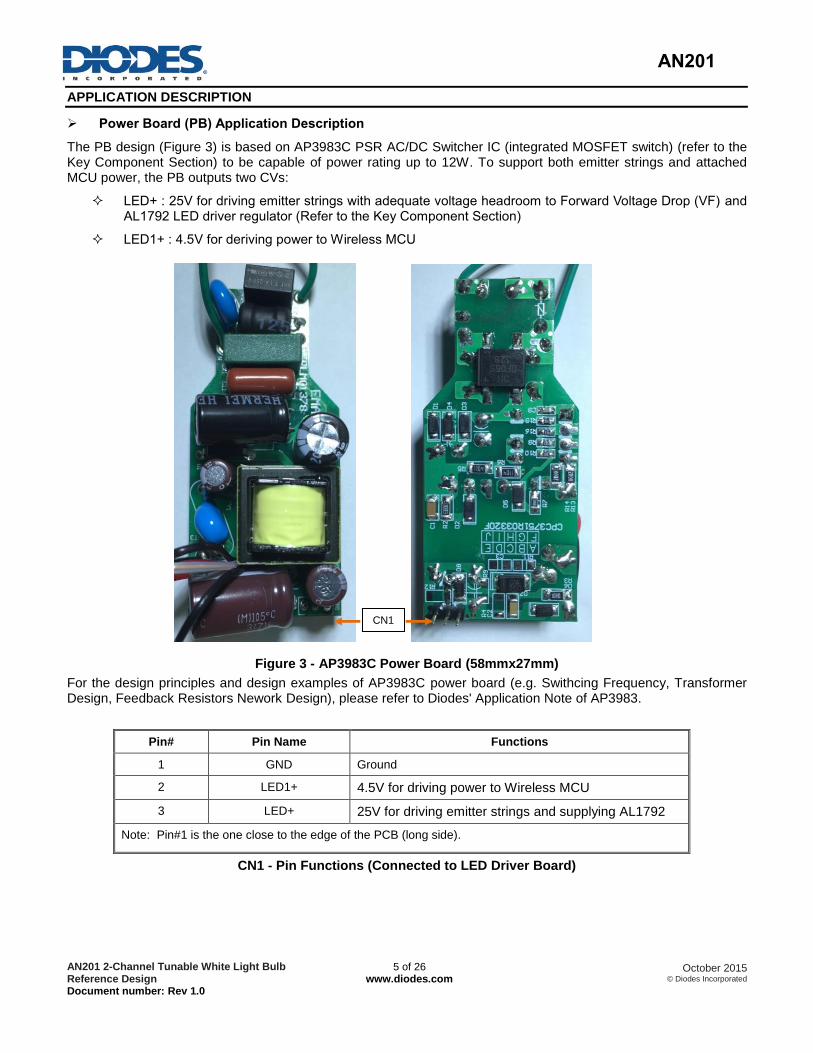
Power Board (PB) Application Description
The PB design (Figure 3) is based on AP3983C PSR AC/DC Switcher IC (integrated MOSFET switch) (refer to the Key Component Section) to be capable of power rating up to 12W. To support both emitter strings and attached MCU power, the PB outputs two CVs:
LED+ : 25V for driving emitter strings with adequate voltage headroom to Forward Voltage Drop (VF) and AL1792 LED driver regulator (Refer to the Key Component Section)
LED1+ : 4.5V for deriving power to Wireless MCU
Figure 3 - AP3983C Power Board (58mmx27mm)
For the design principles and design examples of AP3983C power board (e.g. Swithcing Frequency, Transformer Design, Feedback Resistors Nework Design), please refer to Diodes' Application Note of AP3983.
Pin# Pin Name Functions
1 GND Ground
2 LED1+ 4.5V for driving power to Wireless MCU
3 LED+ 25V for driving emitter strings and supplying AL1792
Note: Pin#1 is the one close to the edge of the PCB (long side).
CN1 - Pin Functions (Connected to LED Driver Board)
CN1

AN201 2-Channel Tunable White Light Bulb Reference Design Document number: Rev 1.0
6 of 26 www.diodes.com
October 2015 © Diodes Incorporated
AN201
Emitter Module Board (EMB) Application Description
The 2-Ch TW EMB (Figure 4) adopts two types of CCT Emitters, arranged in parallel-serial strings (3P4S - 3 Parallel and 4 Serial Emitters) as follows:
2,700K CCT White Emitters (total of 12 Emitters 4S3P), CCTwarm
6,500K CCT White Emitters (total of 12 Emitters 4S3P), CCTcold
The Forward Voltage Drop (VF) per emitter, with two 0.5W emitter dies in serial, is around 6.0V and the toal VF per emitter sting is 24.0V (refer to Appendix II Emitter Spec). The cathodes of CCTwarm and CCTcold emitter strings are attached to LED1 and LED2 pins of AL1792 IC, respectively.
The choices of numbers of emitters, emitter structure arrangement , and driving current are based on meeting the required system specification (above 800 lumens for the finished light bulb).
Figure 4 - 2-Ch TW Emitter Module (Diameter - 46mm)
Pin# Pin Name Functions
LED+ +25V The soldering pad is attached to the common anode of LED(6500K) and LED(2700K) emitter strings.
LED1- 6500K LED- The soldering pad is attached to the cathode of LED(6500K) emitter string.
LED- 2700K LED- The soldering pad is attached to the cathode of LED(2700K) emitter string.
A1 Antenna The soldering pad is attached to the Antenna chip.
Output / Input Pin Functions

AN201 2-Channel Tunable White Light Bulb Reference Design Document number: Rev 1.0
7 of 26 www.diodes.com
October 2015 © Diodes Incorporated
AN201
LED Driver Board (LDB) Application Description
In this 2-Ch TW SCL bulb design, the REF (reference current setting resistor) for LED Driver circuit is 9.1KΩ (R4 in Figure 2.b) to regulate a total channel current around 330mA for both LED1 and LED2 of AL1792. The LED input power for each fixed CCT emitter strings is around 8.0W (24V*330mA). By applying suitable PWM signal patterns to both CCTwarm and CCTcold emitter strings (2,700K and 6,500K), CCT tuning ranging from 2,700K to 6,500K can be achieved.
Note that an wireless chip antenna (A1) is placed on the EMB for wireless connectivity.
Figure 5 - AL1792 LED Driver Module (30mmx24mm)
Pin# Pin Name Functions
1 GND Ground.
2 LED1+ 4.5V input, supplying LDO for Wireless MCU.
3 LED+ 25V input, for driving emitter strings and supplying AL1792
CN1 - Pin Functions (Connected to Power Board)
Pin# Pin Name Functions
1 3.3V This Pin is attached to the output 3.3V of LDO,
For M56 ZigBee module VDD input.
2 GND Ground
3 PWM1
This pin is attached to the PWM1 of U2_AL1792,
Connected to PWM_01 of M56 ZigBee Module, for controlling 6500K emitter string.
4 PWM2
This pin is attached to the PWM2 of U2_AL1792,
Connected to PWM_02 of M56 ZigBee Module, for controlling 2700K emitter string.
5 PWM3 This pin is attached to the PWM3 of U2_AL179X,
Connected to PWM_03 of M56 ZigBee Module.
CN1
CN3
CN2

AN201 2-Channel Tunable White Light Bulb Reference Design Document number: Rev 1.0
8 of 26 www.diodes.com
October 2015 © Diodes Incorporated
AN201
6 PWM4 This pin is attached to the PWM4 of U2_AL179X,
Connected to PWM_04 of M56 ZigBee Module
7 EN
This pin is attached to the EN of U2_AL1792,
Connected to GPIO of M56 ZigBee, to control on/off function of U2_AL1792.
CN2 and CN3- Pin Functions (Connected to ZigBee Module)
Pin# Pin Name Functions
LED+ +25V 25V, for driving emitter strings.
LED1+ +4.5V 4.5V, (Reserved for future use)
LED1- 6500K LED- This soldering pad is attached to the LED1 pin of U2_AL1792, and connected to the cathode terminal of LED1- (6,500K).
LED- 2700K LED- This soldering pad is attached to the LED2 pin of U2_AL1792, and connected to the cathode terminal of LED- (2,700K).
LED2- LED3 This soldering pad is attached to the LED3 pin of U2_AL179X,Connected to LED cathode terminal (Reserved for future use)
LED3- LED4 This soldering pad is attached to the LED4 pin of U2_AL179X,Connected to LED cathode terminal (Reserved for future use)
Output / Input Pin Functions ( Connected LED Emitter Board)
M56 Zigbee Module (ZM) Application Description
For the wireless connectivity, it is enabled by embedding M56 ZigBee Module (Appendix III) inside the 2-ch TW SCL bulb by piggybacking on the other side of the AL1792 LED driver board. Embedded ZigBee Light Link (ZLL) in the flash memory, M56 ZigBee module will communicate ZLL commands with a ZLL-capable Gateway Hub.
This ZigBee module board is piggybacking on the LED driver board on the side opposited to the Power Board.
Figure 6 - M56 ZigBee Module (15mm x 15mm)
Pin1~7 Connected to CN2.
1 2 3 4 5 6 7

AN201 2-Channel Tunable White Light Bulb Reference Design Document number: Rev 1.0
9 of 26 www.diodes.com
October 2015 © Diodes Incorporated
AN201
Output Assembly Description
Figure 7 - Power Board + LED Driver Board + M56 ZigBee board
Two green wires connected to AC input
Three wires for Emitter:
1. Yellow wire connected to LED’s Common Anode
2. Black wire connected to LED_ 2700K cathode
3. White wire connected to LED_ 6500K cathode
Antenna Cable from M56 Zigbee Module connected to A1 ”Antenna Chip” of Emitter board
Antenna cable
2700K cathode
6500K cathode
LEDs Common Anode
CN1
CN2
CN3

AN201 2-Channel Tunable White Light Bulb Reference Design Document number: Rev 1.0
10 of 26 www.diodes.com
October 2015 © Diodes Incorporated
AN201
PERFORMANCE TESTING
The key system performance parameters of 2-ch TW SCL bulb are summarized in Table 1 below.
10W A19 2-Channel Tunable White Reference Light Bulb
Item No Parameter Condition Test Result
1 Input Voltage Range 100-240VAC ~ 50/60Hz
2 Power Factor > 0.7 (LED1: 330mA, LED2: No Load)
110VAC: 0.85 230VAC: 0.73
3 Efficiency - PB Only ~ 85%
(at LED1: 330mA, LED2: No Load)
110VAC: 82.15% 230VAC: 84.9%
4 Standby Power < 0.5Watt (M56 ZigBee module Operating Current is about 33mA )
110VAC/60Hz: 378mW;
230VAC/50Hz: 450mW
5 Start-Up Time
from Wall Switch
110VAC
(1.1MΩ+1.1MΩ Startup Resistor) 1.33 Sec
6 Output Ripple Voltage
(Vpeak-to-peak)
Test Condition at 230 VAC
LED1: 330mA
LED2: 40mA
LED+_25V: 90mV (±1.9%)
LED1+_5V: 56mV (±1.2%)
7 THD (Total Harmonic Distortion)
Test Condition
LED1: 330mA
LED2: No Load
110VAC/60Hz: 51.58%
230VAC/50Hz: 72.21%
8 Temperature of AL1792 < 105°C 70°C (Open Cover)
9 Line Regulation LED+_25V = 26.06~24.93V
LED1+_5V = 5.46~5.09V
10 Load Regulation LED+_25V = 26.06~22.7V
LED1+_5V = 5.46~3.8V
Table 1 - System Performance Testing of 2-ch TW SCL Bulb

AN201 2-Channel Tunable White Light Bulb Reference Design Document number: Rev 1.0
11 of 26 www.diodes.com
October 2015 © Diodes Incorporated
AN201
Using a light measurment device (e.g. Integrating Sphere), key parameters of light outputs for a 2-Ch TW SCL bulb is measured and summarized in Table 2.
Based on the measured results, we could conclude that:
A19 10W 2-Ch TW SCL bulb could deliver desired output (over 800 lumens) at reasonable light quality (CRI > 80) and achieve a CCT Tuning with range from 2,700K to 6,500K with acceptable result (Duv < 0.006). The metric "Duv" is primarily used in connection with the expression of a “generally white” chromaticity in terms of CCT and Planckian locus offset.
No. 1 2 3 4 5 6 7 8 9 10 11
PWM cold (%) 0% 10% 20% 30% 40% 50% 60% 70% 80% 90% 100%
PWM warm (%) 100% 90% 80% 70% 60% 50% 40% 30% 20% 10% 0%
Lumen 824 826 843 872 883 882 892 886 878 870 864
Efficacy
(Lumen/Watt) 78.40 79.19 80.98 83.77 84.74 84.56 85.60 85.03 84.18 83.49 82.52
CCT (K) 2675 2874 3094 3331 3600 3909 4243 4637 5098 5622 6243
CIE x 0.4634 0.4446 0.4274 0.4119 0.3969 0.3824 0.3692 0.3558 0.3424 0.3297 0.3168
CIE y 0.4136 0.4039 0.3953 0.3875 0.3796 0.3719 0.3652 0.3579 0.3502 0.3434 0.3366
CIE u' 0.2634 0.2556 0.2482 0.2414 0.2348 0.2284 0.2223 0.2162 0.2102 0.2041 0.1978
CIE v' 0.529 0.5225 0.5164 0.5109 0.5053 0.4997 0.4947 0.4893 0.4836 0.4783 0.4729
Duv 0.0008 -0.0010 -0.0022 -0.0028 -0.0031 -0.0029 -0.0021 -0.0010 0.0004 0.0024 0.0050
Ra 81.4 83.1 84.6 85.8 86.6 87.0 87.0 86.8 86.2 85.6 84.2
Input Power (W) 10.51 10.43 10.41 10.41 10.42 10.43 10.42 10.42 10.43 10.42 10.47
PF 0.883 0.883 0.883 0.883 0.883 0.882 0.882 0.882 0.882 0.883 0.883
V LED+ (V) 24.7 24.7 24.7 24.7 24.7 24.7 24.7 24.7 24.7 24.7 24.7
I LED+ (mA) 344 342 342 342 342 342 342 342 342 342 342
Headroom (2700K)
V_LED- _ON [V]
1.28 1.14 1.14 1.14 1.02 0.98 0.90 0.86 0.82 1.02 N/A
Headroom (6500K)
V_LED1- _ON [V]
N/A 1.00 0.84 0.84 0.84 0.84 0.84 0.84 0.88 0.98 0.98
Table 2 - Light Output Measurement of 2-Ch TW SCL Bulb @110VAC

AN201 2-Channel Tunable White Light Bulb Reference Design Document number: Rev 1.0
12 of 26 www.diodes.com
October 2015 © Diodes Incorporated
AN201
SYSTEM DESIGN CONSIDERATIONS AND TRADE-OFFS
When design a production worthy SCL bulb, the system designers have many considerations:
1) Input Voltage Range
2) Power Factor (PF)
3) Efficiency
4) Standby Power
5) Start-Up Time
6) Thermal Management
While 2-ch TW SCL bulb is designed for full range voltage input, system designs could optimize components for single voltage application (e.g. 120V or 230V). For example, more cost-effective components could be used for 120V-only SCL bulb, including:
1) BD1 (DF06S)
2) Passive Valley Fill (PVF) Circuit: C4, C6, D1, D3 and D4 (see figure 2.a on page 3)
AP3983C, with integrated MOSFET switch, has its advantages of supporting a cost-effective power board design. The relative small ripple of output voltage for CVs of AP3983C (Vpeak-to-peak ripple < 2.9% of the CV of Emitter Strings) is ideal to support linear Constant Current Regulation (CCR) based LED driver, such as AL1792, with optimal voltage headroom for attached LED emitter strings.
Per Energy Start Compliance requirement, the Power Factor (PF) for over 5W light bulb need to be over 0.70. As the AP3983C does not have built-in Active Power Factor circuitry, a PVF Circuit, consists of C4, C6. D1, D3 and D4 is designed to achieve desired PF over 0.7. A high PF value could be achieved by using larger capacitors (C4 and C6), however the trade-offs will be a longer start-up time, PCB space and cost. The system designers need to select the right balance for the PF value and other considerations.
The system efficiency of 10W typical 2-ch TW SCL bulb needs to be above 75% based on the proposed two-stage designs. For the Power stage (first stage) efficiency, it is designed to achieve 85%. The factors impacting power board efficiency include:
1) CV Output Voltage
2) Pre-loading circuit (D8, R4, R9 and R12, see figure 2.a on page 3) to prevent spurious output voltage at no load situation for one CV output, but sudden current is drawn by the other CV output.
3) Low VF Drop Super Barrier Rectifier (D6, D7, see figure 2.a on page 3)
While fixed-CCT on-off LED light bulb will have no power consumption when turned off at standby mode, a SCL bulb consumes non-trivial standby power due to constant-on for wireless module connectivity. To save energy consumed during the standby mode, it recommded to stay within 0.5W when in the standby mode for the entire SCL bulb.
In the 2-ch TW SCL bulb design, the standby power consumption is measured with estimated breakdown as follows:
1) AL1792 IC - 50 mW (Quiescent Supply Current of AL1792 EN Enable)
2) Dummy Loading - 50 mW (Added 22V zener diode between LED+ and LED1+)
3) Start-up Resistor Circuit - 50 mW (R5 and R6 are 1M/1206 resistor)
4) ZigBee Module - 300 mW (UBEC M56 ZigBee Module standby current is 35mA)
5) Others Power Loss- 50 mW (AP3983, Snubber and Switching Loss)

AN201 2-Channel Tunable White Light Bulb Reference Design Document number: Rev 1.0
13 of 26 www.diodes.com
October 2015 © Diodes Incorporated
AN201
Improved Power Consumption Suggestion
Startup Circuit
For low-cost implementation, a simple start-up circuity is adopted (R5 and R6, see figure 2.a on page 3). Trade-offs involved are start-up time (time when LED light could be turned on upon instruction to actual light output) and standby power consumption. Increasing the value of resistance of R5 and R6, the standby power will decrease at the expense of longer start-up time (Table 3).
Values of R5 & R6 startup time at 110VAC
(after fully whole circuit discharged)
Standby Power at 230VAC
LED OFF Mode (<0.5W)
two 1.1M = 2.2MΩ 1.33 Sec 450 mW
two 510K = 1020KΩ 0.62 Sec 470 mW
two 392K = 784KΩ 0.20 Sec 508 mW
*Vcc cap(C7)=4.7uF/50V
Table 3 - Start-Up Resistor Circuit on Startup Time and Standby Power
An alternative quick dynsmic startup circuit can be used to replace the resistor start-up circuit to shorten start-up time without static standby power consumption (Figure 7). During the AC power initial input, Transistor Q1 is turned ON to charge VCC input to AP3983C. Q1 will be shut off after initial start-up time until shut off by returning path from the auxiliary winding when VCC is highter than one threshold voltage below 18V where the Zener diode is clamped at.
HV
VCC
R1 R2
Q1
BSS127
ZD1
DFLZ18
Figure 7 - Dynamic Fast Start-Up Circuit
AL1792 Standby consumption
MCU can enable/disable the “EN” (Enable Pin) to save power while the AL1792 IC is in standby mode.
Input AC AL1792 Standby Power
With EN Enable
AL1792 Standby Power
With EN Disable Improved Power Saving
At 110VAC 378mW 350mW 28mW
At 230VAC 450mW 425mW 25mW
Table 4 - AL1792 Enable/Disable Power Consumption

AN201 2-Channel Tunable White Light Bulb Reference Design Document number: Rev 1.0
14 of 26 www.diodes.com
October 2015 © Diodes Incorporated
AN201
Thermal Management Design Suggestion
Thermal management is a critical design consieration as it impacts safety and reliability of the SCL bulbs. Among many good practices used in the power board design for managing thermal issues of SCL bulbs, system designers also need to fine tune the CV output to compensate for VF fluctuation due to temperature effect. Depending on thermal characteristics of emitters, VF drops around 5% to 10% range when temperature is increased from 25°C to 125°C. The proposed design is based on a low-cost open-loop CV fine tuning approach by adopting a Negative Temperature Coeffient (NTC) resistor 10K (The Circuit is not shown). The CV output of The 2-ch TW SCL bulb design is in the range of 25V down to 23.5V.
Figure 8 - Thermal Management Circuit
R16
47K
R10 10K
T1EE16
1
4
3
2
PT1
PT2
PT3
(NTC)
R1513K
R8 5.6K
U1AP3983C/DIP-7
1
2
3
4
5,6
7
CP
C
FB
VC
C
CS
D
GND

AN201 2-Channel Tunable White Light Bulb Reference Design Document number: Rev 1.0
15 of 26 www.diodes.com
October 2015 © Diodes Incorporated
AN201
KEY COMPONENTS
AP3983C - AC/DC Controller
AP3983C IC PIN OUT ASSIGNMENT
Primary Side control for Eliminating Opto-coupler and Secondary CV/CC Control Circuitry
Built-In HV power MOSFET with 650V BVdss
Valley-turn on to reduce switching loss
Up to 80KHz operating frequency at full load for compact size application
Piece-wise frequency reduction to enhance conversion efficiency and suppress audio noise
±5% constant voltage accuracy
±7% constant current accuracy
Open Circuit Protection (OCP), Over Voltage Protection (OVP), Over Temperature Protection (OTP)
Short Circuit Protection (SCP) with hiccup
3-Segment Drive Current for Radiative EMI Suppression
Pin Symbol Descriptions
Name SO-7 / PDIP-7
CPC 1 This pin is connected a capacitor to GND to serve as a cable compensation function. Additional resistor in parallel with the capacitor will weaken cable compensation to meet cable-less applications.
FB 2 The voltage feedback is from Auxiliary winding.
VCC 3 This pin receives rectified voltage from the Auxiliary winding of the transformer.
CS 4 It is used for current sense from primary side of the transformer.
D 5, 6 The pin is connected with an internal power MOSFET's drain.
GND 7 The pin is the signal reference ground.

AN201 2-Channel Tunable White Light Bulb Reference Design Document number: Rev 1.0
16 of 26 www.diodes.com
October 2015 © Diodes Incorporated
AN201
AL1791/2/3/4 - LED Driver Controller
AL1791/2/3/4 IC PIN OUT ASSIGNMENT
EN
PWM4/GND
PWM3/GND
PWM2/GND
PWM1
LED1
LED2/GND
VIN
REF
FAULTB
LEDPG
LED4/GND
LED3/GND
GND
1
2
3
4
5
6
7 8
9
10
11
12
13
14
Input Voltage Range: 6.5V to 30V
1/2/3/4-channel LED drivers: independent Analog or PWM dimming control for each channel
Reference Current: Adjustable by an external reference resistor
Ratio-optimized currents for 4 independent LED channels (AL1794 only): Suitable for Tunable White and Tunable Color
Low Standby Power: With EN pin
E-flicker free High Frequency PWM dimming with Deep Dimming Capability: Support 10KHz down to 1.0%, 4KHz down to 0.4%, or 1KHz down to 0.1%
Internal Protections: Under Voltage Lockout (UVLO), LED string open/short protection
Over temperature protection (OTP): Thermal shut down and auto thermal recovery
Fault Reporting: UVLO, OTP, Open, and Short
LED Power Good Reporting
Low system BOM cost
Ambient Temperature Range -40°C to +125°C (Automotive Grade)
U-DFN4030-14: Available in “Green” Molding Compound (No Br, Sb)
Totally Lead-Free & Fully RoHS Compliant
Halogen and Antimony Free. “Green” Device

AN201 2-Channel Tunable White Light Bulb Reference Design Document number: Rev 1.0
17 of 26 www.diodes.com
October 2015 © Diodes Incorporated
AN201
AL1791/2/3/4 Pin Descriptions
Pin Part Number Descriptions
Name U-DFN4030-14
EN 1 Active-high to Enable, Internally Pulled Down.
PWM4/GND 2 PWM Signal Input for channel 4, Internally pulled down for AL1794. GND for AL1791, AL1792, and AL1793.
PWM3/GND 3 PWM Signal Input for channel 3, Internally pulled down for AL1793 and AL1794. GND for AL1791 and AL1792.
PWM2/GND 4 PWM Signal Input for channel 2, Internally pulled down for AL1792, AL1793, and AL1794. GND for AL1791.
PWM1 5 PWM Signal Input for channel 1, Internally pulled down (Tied to GND when this channel is NOT used).
LED1 6 Channel 1 LED Cathode.
LED2/GND 7 Channel 2 LED Cathode for AL1792, AL1793, and AL1794. GND for AL1791.
GND 8 Ground.
LED3/GND 9 Channel 3 LED Cathode for AL1793 and AL1794. GND for AL1791 and AL1792.
LED4/GND 10 Channel 4 LED Cathode for AL1794. GND for AL1791, AL1792, and AL1793.
LEDPG 11 LED Power Good Indication. Asserted low to report insufficient headroom. Needs an external pull-up resistor.
FAULTB 12 Fault Report. Asserted Low to report faulty conditions. Needs an external pull-up resistor.
REF 13 Reference Current Setting through External Resistor (RSET).
VIN 14 Voltage Input
Exposed PAD Exposed PAD
Exposed pad. Internally connected to GND.
It should be externally connected to GND and thermal mass for enhanced thermal impedance.
It should not be used as electrical conduction path.
AN201 2-Channel Tunable White Light Bulb Reference Design Document number: Rev 1.0
18 of 26 www.diodes.com
October 2015 © Diodes Incorporated
AN201
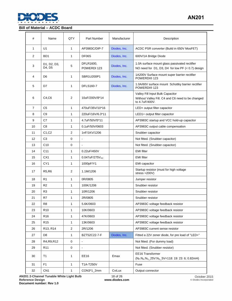
Bill of Material – ACDC Board
# Name QTY Part Number Manufacturer Description
1 U1 1 AP3983C/DIP-7 Diodes, Inc. ACDC PSR converter (Build in 650V MosFET)
2 BD1 1 DF06S Diodes, Inc. 600V/1A Bridge Diode
3 D1, D2, D3, D4, D5
5 DFLR1600,
POWERDI 123 Diodes, Inc.
1.0A surface mount glass passivated rectifier
NO need for D1, D3, D4 for low PF (< 0.7) design
4 D6 1 SBR1U200P1 Diodes, Inc. 1A200V Surface mount super barrier rectifier POWERDI® 123
5 D7 1 DFLS160-7 Diodes, Inc. 1.0A/60V surface mount Schottky barrier rectifier POWERDI® 123
6 C4,C6 2 10uF/200V/8*14
Valley Fill Input Bulk Capacitor
Without Valley Fill. C4 and C6 need to be changed to 4.7uF/400V.
7 C5 1 470uF/35V/10*16
LED+ output filter capacitor
8 C9 1 220uF/16V/6.3*11 LED1+ output filter capacitor
9 C7 1 4.7uF/50V/5*11 AP3983C startup and VCC hold-up capacitor
10 C8 1 0.1uF/50V/0603 AP3983C output cable compensation
11 C1,C2 2 1nF/1KV/1206 Snubber capacitor
12 C3 0 - Not fitted. (Snubber capacitor)
13 C10 0 -
Not fitted. (Snubber capacitor)
14 C11 1 0.22uF/450V
EMI filter
15 CX1 1 0.047uF/275VAC EMI filter
16 CY1 1 1000pF/Y1 EMI capacitor
17 R5,R6 2 1.1M/1206 Startup resistor (must for high voltage stress >200V)
18 R1 1 0R/0805
Jumper resistor
19 R2 1 100K/1206 Snubber resistor
20 R3 1 10R/1206 Snubber resistor
21 R7 1 2R/0805
Snubber resistor
22 R8 1 5.6K/0603
AP3983C voltage feedback resistor
23 R10 1 10K/0603
AP3983C voltage feedback resistor
24 R16 1 47K/0603 AP3983C voltage feedback resistor
25 R15 1 13K/0603 AP3983C voltage feedback resistor
26 R13, R14 2 2R/1206 AP3983C current sense resistor
27 D8 1 BZT52C22-7-F Diodes, Inc. Fitted a 22V zener diode, for pre load of "LED+"
28 R4,R9,R12 0 - Not fitted. (For dummy load)
29 R11 0 -
Not fitted. (Snubber resistor)
30 T1 1 EE16 Emax EE16 Transformer
(NP:NA:NS_25V:NS_5V=118: 19: 23: 6; 0.82mH)
31 F1 1 T1A-T250V Fuse
32 CN1 1 CON3*1_2mm CviLux Output connector
AN201 2-Channel Tunable White Light Bulb Reference Design Document number: Rev 1.0
19 of 26 www.diodes.com
October 2015 © Diodes Incorporated
AN201
(CH1101S)
33 L1 1 1.0mH/6Φ I core EMI filter inductance
34 VDR1 1 471K Surge Absorber
TOTAL
38 Power Board Electronic Parts
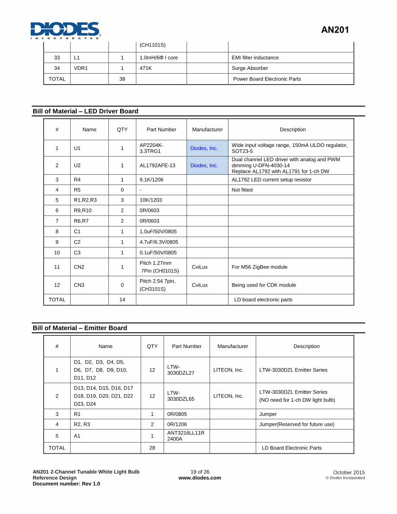
Bill of Material – LED Driver Board
# Name QTY Part Number Manufacturer Description
1 U1 1 AP2204K-3.3TRG1
Diodes, Inc. Wide input voltage range, 150mA ULDO regulator, SOT23-5
2 U2 1 AL1792AFE-13 Diodes, Inc. Dual channel LED driver with analog and PWM dimming U-DFN-4030-14 Replace AL1792 with AL1791 for 1-ch DW
3 R4 1 9.1K/1206
AL1792 LED current setup resistor
4 R5 0 -
Not fitted
5 R1,R2,R3 3 10K/1203
6 R9,R10 2 0R/0603
7 R6,R7 2 0R/0603
8 C1 1 1.0uF/50V/0805
9 C2 1 4.7uF/6.3V/0805
10 C3 1 0.1uF/50V/0805
11 CN2 1 Pitch 1.27mm
7Pin (CH0101S) CviLux For M56 ZigBee module
12 CN3 0 Pitch 2.54 7pin,
(CH3101S) CviLux Being used for CDK module
TOTAL
14 LD board electronic parts
Bill of Material – Emitter Board
# Name QTY Part Number Manufacturer Description
1
D1, D2, D3, D4, D5,
D6, D7, D8, D9, D10,
D11, D12
12 LTW-3030DZL27
LITEON, Inc. LTW-3030DZL Emitter Series
2
D13, D14, D15, D16, D17
D18, D19, D20, D21, D22
D23, D24
12 LTW-3030DZL65
LITEON, Inc. LTW-3030DZL Emitter Series
(NO need for 1-ch DW light bulb)
3 R1 1 0R/0805
Jumper
4 R2, R3 2 0R/1206 Jumper(Reserved for future use)
5 A1 1 ANT3216LL11R2400A
TOTAL
28 LD Board Electronic Parts

AN201 2-Channel Tunable White Light Bulb Reference Design Document number: Rev 1.0
20 of 26 www.diodes.com
October 2015 © Diodes Incorporated
AN201
APPENDIX I - EE16 TRANSFORMER SPEC
EE16 transformer with (Appendix X).
A. Transformer Pin & Wire Description:
Circuit: Cross sectional view:
8
2
L2
1
L1
PT2
PT4
PT1
L5
4
3PT3
L4L3
3F1
Start
Teflon Tube
Primary Secondary
L1
F1 Wire Shilding
L5
L4+L5
L3
L2
1T
2Ts
2Ts
2Ts
2Ts
3Ts
Over core
Pin definition (StartEnd)
Wire (φ) Turn (Ts) Layers Layers of Tape
L1 1 8 2UEW-B 0.21mm x 1P 72 2 1T
F1 3 2UEW-B 0.1mm x 1P 75 1 2Ts
L5 PT2 PT1 Triple wire-B 0.35mm x 1P 23 1.5
L4 PT3 PT4 Triple wire-B 0.35mm x 1P 6 0.5 2Ts
L3 3 4 2UEW-B 0.2mm x 1P 19 1 2Ts
L2 8 2 2UEW-B 0.21mm x 1P 46 2 2Ts
OVER CORE
B. Electrical Characteristic :
# Test Item Winding Pin Rating Unit Tolerance Remark
2.1 Inductance L1 and L2 1 → 2 0.82 mH +/-5% @ 100KHz / 1V

AN201 2-Channel Tunable White Light Bulb Reference Design Document number: Rev 1.0
21 of 26 www.diodes.com
October 2015 © Diodes Incorporated
AN201
APPENDIX II - LITEON OPTO 2-CHANNEL TW EMITTER MODULE
LTW-3030DZL Emitter Series (LTW-3030DZL27 and LTW-3030DZL65) -
Typical Performance
AN201 2-Channel Tunable White Light Bulb Reference Design Document number: Rev 1.0
22 of 26 www.diodes.com
October 2015 © Diodes Incorporated
AN201
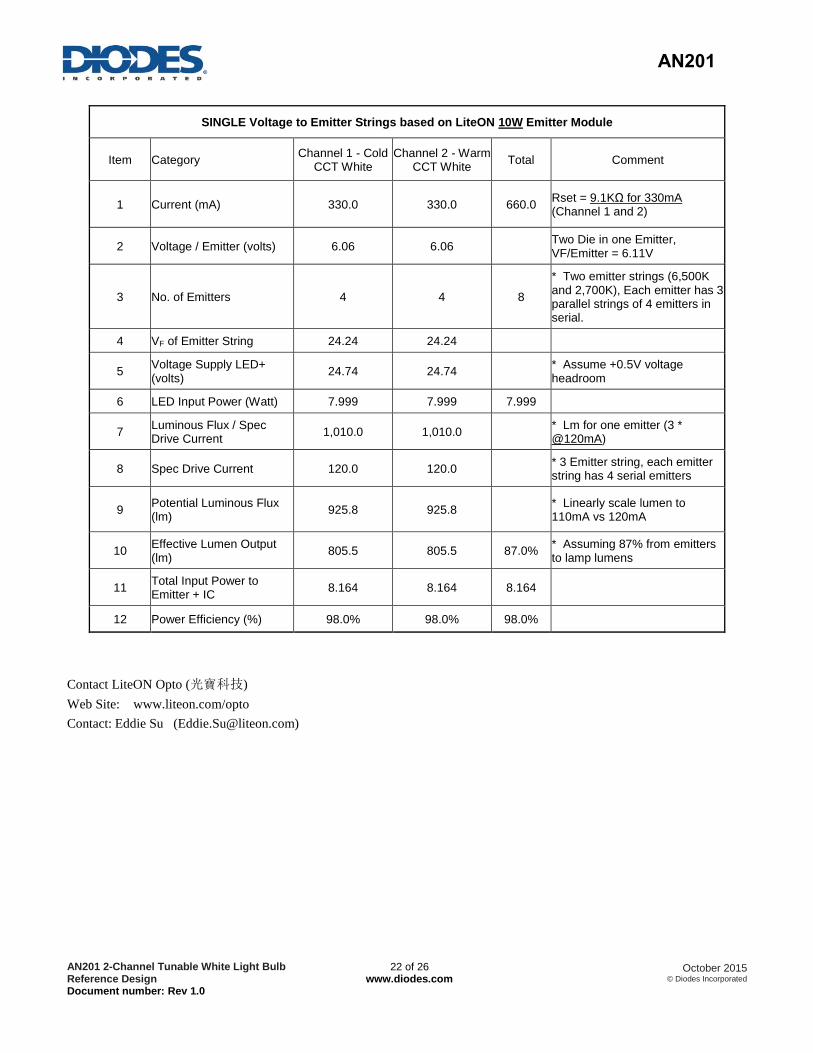
SINGLE Voltage to Emitter Strings based on LiteON 10W Emitter Module
Item Category Channel 1 - Cold
CCT White Channel 2 - Warm
CCT White Total Comment
1 Current (mA) 330.0 330.0 660.0 Rset = 9.1KΩ for 330mA (Channel 1 and 2)
2 Voltage / Emitter (volts) 6.06 6.06
Two Die in one Emitter, VF/Emitter = 6.11V
3 No. of Emitters 4 4 8
* Two emitter strings (6,500K and 2,700K), Each emitter has 3 parallel strings of 4 emitters in serial.
4 VF of Emitter String 24.24 24.24
5 Voltage Supply LED+ (volts)
24.74 24.74
* Assume +0.5V voltage headroom
6 LED Input Power (Watt) 7.999 7.999 7.999
7 Luminous Flux / Spec Drive Current
1,010.0 1,010.0
* Lm for one emitter (3 * @120mA)
8 Spec Drive Current 120.0 120.0
* 3 Emitter string, each emitter string has 4 serial emitters
9 Potential Luminous Flux (lm)
925.8 925.8
* Linearly scale lumen to 110mA vs 120mA
10 Effective Lumen Output (lm)
805.5 805.5 87.0% * Assuming 87% from emitters to lamp lumens
11 Total Input Power to Emitter + IC
8.164 8.164 8.164
12 Power Efficiency (%) 98.0% 98.0% 98.0%
Contact LiteON Opto (光寶科技)
Web Site: www.liteon.com/opto
Contact: Eddie Su ([email protected])

AN201 2-Channel Tunable White Light Bulb Reference Design Document number: Rev 1.0
23 of 26 www.diodes.com
October 2015 © Diodes Incorporated
AN201
APPENDIX III - ZIGBEE MODULE M56 (UBEC)
Introduction and Specification
M56 Module: 2.4GHz RF module which integrates UBEC’s low power 2.4GHz
IEEE802.15. 4 RFIC UZ2400D
MCU: ARM M0-Cotex Low Power Design
Voltage Input: 2.7V ~ 3.6V
TX Current (@3.3V, 32MHz): 37.09mA
RX Current (@3.3V, 32MHz): 33.76mA
Temperature Range: -20°C ~ 105°C
Dimension: 15mm x 15mm
Pin# Pin Name Functions
1 VDD Connected to LED driver board - 3.3V
2 GND Connected to LED driver board Ground
3 PWM_01 Connected to LED driver board – PWM1 of AL1792
To control 6,500K LED
4 PWM_02 Connected to LED driver board – PWM2 of AL1792
To control 2,700K LED
5 PWM_03 Connected to LED driver board – Reserved for future use
6 PWM_04 Connected to LED driver board – Reserved for future use
7 EN Connected to AL1792 Pin#1-EN, Enable AL1792.
Output Pin Functions (Connected to LED Driver Board Module)
M56 ZigBee Module Outline Drawing

AN201 2-Channel Tunable White Light Bulb Reference Design Document number: Rev 1.0
24 of 26 www.diodes.com
October 2015 © Diodes Incorporated
AN201
Schematic and Connection Definition
Pin# Pin Name Functions Remark
1 TX UART1 data transmitter output pin Connected to GPB5
2 RX UART1 data receiver input pin Connected to GPB4
3 NRST RST
4 SWDAT ICE_SWDAT
5 SWCLK ICE_SWCLK
J1 - Serial Wire Debug Port

AN201 2-Channel Tunable White Light Bulb Reference Design Document number: Rev 1.0
25 of 26 www.diodes.com
October 2015 © Diodes Incorporated
AN201
Pin# Pin Name Functions Remarks
1 VDD +3.3V
2 GND Ground
3 PWM_01 PWM 0 channel 0 output, GPIO, (PA. 12) 6,500K
4 PWM_02 PWM 0 channel 1 output, GPIO, (PA. 13) 2,700K
5 PWM_03 PWM 0 channel 2 output, GPIO, (PA. 14)
6 PWM_04 PWM 0 channel 3 output, GPIO, (PA. 15)
7 EN GPIO, I2C 1 SDA, (PA. 10) EN
8 FAULTB GPIO, I2C 1 SCL, (PA. 11)
9 LEDPG GPIO, ADC, (PA. 0)
10 TEM-D Not Available
11 VADJI I/D GPIO, DAC (PC. 7)
J2 - Application Usage
Contact UBEC:
Headquarters
Address: 6F-1, No. 192, Dongguang Rd., Hsinchu, 300 Taiwan
Tel: +886-3-5729898
Fax: +886-3-5718599
Website: http://www.ubec.com.tw
Sales Services
E-mail: [email protected]

AN201 2-Channel Tunable White Light Bulb Reference Design Document number: Rev 1.0
26 of 26 www.diodes.com
October 2015 © Diodes Incorporated
AN201
IMPORTANT NOTICE
DIODES INCORPORATED MAKES NO WARRANTY OF ANY KIND, EXPRESS OR IMPLIED, WITH REGARDS TO THIS DOCUMENT, INCLUDING, BUT NOT LIMITED TO, THE IMPLIED WARRANTIES OF MERCHANTABILITY AND FITNESS FOR A PARTICULAR PURPOSE (AND THEIR EQUIVALENTS UNDER THE LAWS OF ANY JURISDICTION).
Diodes Incorporated and its subsidiaries reserve the right to make modifications, enhancements, improvements, corrections or other changes without further notice to this document and any product described herein. Diodes Incorporated does not assume any liability arising out of the application or use of this document or any product described herein; neither does Diodes Incorporated convey any license under its patent or trademark rights, nor the rights of others. Any Customer or user of this document or products described herein in such applications shall assume all risks of such use and will agree to hold Diodes Incorporated and all the companies whose products are represented on Diodes Incorporated website, harmless against all damages.
Diodes Incorporated does not warrant or accept any liability whatsoever in respect of any products purchased through unauthorized sales channel.
Should Customers purchase or use Diodes Incorporated products for any unintended or unauthorized application, Customers shall indemnify and hold Diodes Incorporated and its representatives harmless against all claims, damages, expenses, and attorney fees arising out of, directly or indirectly, any claim of personal injury or death associated with such unintended or unauthorized application.
Products described herein may be covered by one or more United States, international or foreign patents pending. Product names and markings noted herein may also be covered by one or more United States, international or foreign trademarks.
This document is written in English but may be translated into multiple languages for reference. Only the English version of this document is the final and determinative format released by Diodes Incorporated.
LIFE SUPPORT
Diodes Incorporated products are specifically not authorized for use as critical components in life support devices or systems without the express written approval of the Chief Executive Officer of Diodes Incorporated. As used herein:
A. Life support devices or systems are devices or systems which:
1. are intended to implant into the body, or
2. support or sustain life and whose failure to perform when properly used in accordance with instructions for use provided in the labeling can be reasonably expected to result in significant injury to the user.
B. A critical component is any component in a life support device or system whose failure to perform can be reasonably expected to cause the
failure of the life support device or to affect its safety or effectiveness.
Customers represent that they have all necessary expertise in the safety and regulatory ramifications of their life support devices or systems, and acknowledge and agree that they are solely responsible for all legal, regulatory and safety-related requirements concerning their products and any use of Diodes Incorporated products in such safety-critical, life support devices or systems, notwithstanding any devices- or systems-related information or support that may be provided by Diodes Incorporated. Further, Customers must fully indemnify Diodes Incorporated and its representatives against any damages arising out of the use of Diodes Incorporated products in such safety-critical, life support devices or systems.
Copyright © 2015, Diodes Incorporated
www.diodes.com