Embed Size (px)
Citation preview
UNIT II
Ajay Kumar GautamAsst. Prof.Electronics & Communication EngineeringDev Bhoomi Institute of Technology & Engineering Dehradun
Syllabus
EPITAXIAL PROCESS: Epitaxy and its concept, Growth kinetics of epitaxy, epitaxial growth, Low temperature epitaxy, Si-epitaxy- growth chemistry of Si epitaxial layer, auto-doping apparatus for epitaxial layer, apparatus for epitaxy, MBE system
DIFFUSION PROCESS: Diffusion models of solid, Fick’s theory of diffusion, Solution of Fick`s Law, diffusion parameters measurements schemes,
ION IMPLANTATION: Scattering phenomenon, range theory, channeling, implantation damage, ion-implantation systems, Annealing
Friday, September 6, 2013By: Ajay Kumar Gautam, DBITE, Dehradun 1
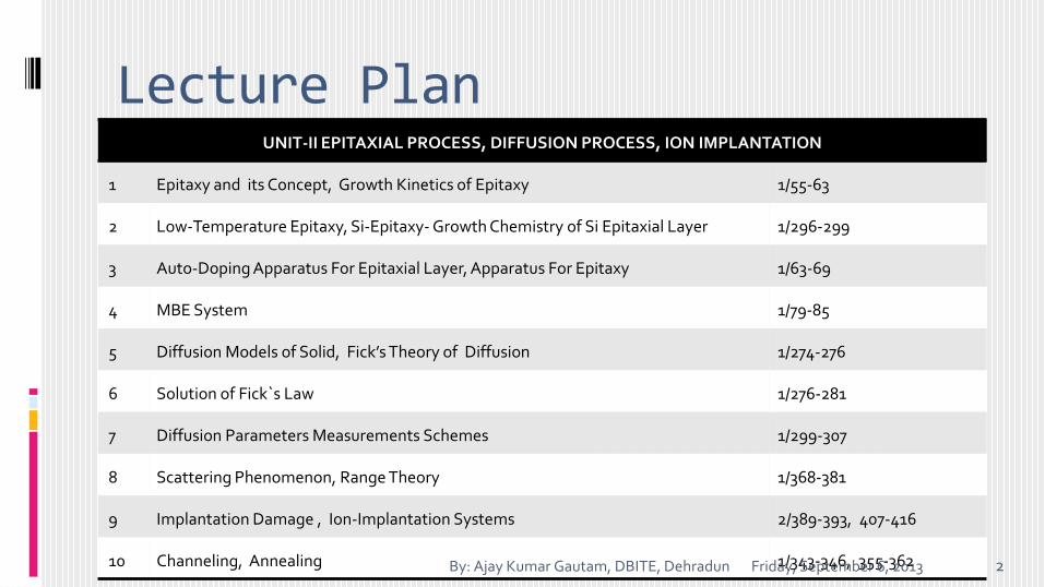
Lecture PlanUNIT-II EPITAXIAL PROCESS, DIFFUSION PROCESS, ION IMPLANTATION
1 Epitaxy and its Concept, Growth Kinetics of Epitaxy 1/55-63
2 Low-Temperature Epitaxy, Si-Epitaxy- Growth Chemistry of Si Epitaxial Layer 1/296-299
3 Auto-Doping Apparatus For Epitaxial Layer, Apparatus For Epitaxy 1/63-69
4 MBE System 1/79-85
5 Diffusion Models of Solid, Fick’s Theory of Diffusion 1/274-276
6 Solution of Fick`s Law 1/276-281
7 Diffusion Parameters Measurements Schemes 1/299-307
8 Scattering Phenomenon, Range Theory 1/368-381
9 Implantation Damage , Ion-Implantation Systems 2/389-393, 407-416
10 Channeling, Annealing 1/343-346, 355-362Friday, September 6, 2013By: Ajay Kumar Gautam, DBITE, Dehradun 2
Module 1
Friday, September 6, 2013By: Ajay Kumar Gautam, DBITE, Dehradun 3
EPITAXIAL PROCESS
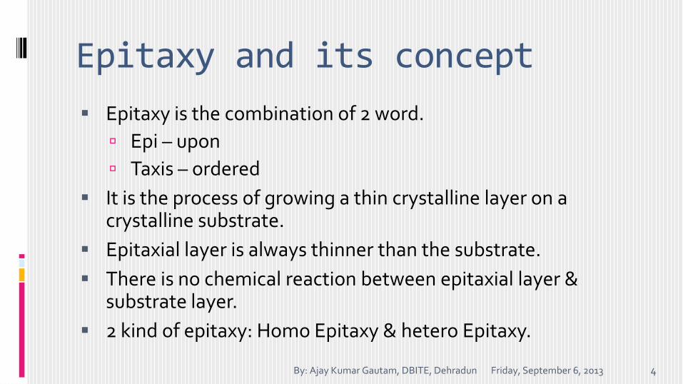
Epitaxy and its concept
Epitaxy is the combination of 2 word.
Epi – upon
Taxis – ordered
It is the process of growing a thin crystalline layer on a crystalline substrate.
Epitaxial layer is always thinner than the substrate.
There is no chemical reaction between epitaxial layer & substrate layer.
2 kind of epitaxy: Homo Epitaxy & hetero Epitaxy.
Friday, September 6, 2013By: Ajay Kumar Gautam, DBITE, Dehradun 4
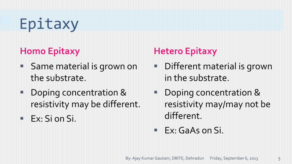
Epitaxy
Homo Epitaxy Hetero Epitaxy
Same material is grown on the substrate.
Doping concentration & resistivity may be different.
Ex: Si on Si.
Different material is grown in the substrate.
Doping concentration & resistivity may/may not be different.
Ex: GaAs on Si.
Friday, September 6, 2013By: Ajay Kumar Gautam, DBITE, Dehradun 5
Techniques for Epitaxy
In VLSI, there are 3 techniques to grow epitaxial layer.
1. Liquid Phase Epitaxy (LPE)
2. Vapor Phase Epitaxy (VPE)
3. Molecular Beam Epitaxy (MBE)
In LPE & VPE, there a some chemical reactions involved but in MBE there is no chemical reaction involved.
MBE is a physical evaporation process.
In VPE, the material which we want to grow on the Si substrate must be in vapor form.
LPE mainly used to grow GaAs on Si.
Friday, September 6, 2013By: Ajay Kumar Gautam, DBITE, Dehradun 6
Epitaxial Growth
The material which we want to grow on the substrate must be in vapor form.
We use some gases & chemical reactants.
Liquid with very high vapor pressure instead of gas may also be used.
We have a graphite susceptor on which substrate (samples) are placed inside a reactor.
Also, we have a flow of gas.
The gas is containing the reactants.
As the reactants flow over the samples, there will be deposition at the top of the samples.
This process is called “Vapor Phase Epitaxy”.
Friday, September 6, 2013By: Ajay Kumar Gautam, DBITE, Dehradun 7
Friday, September 6, 2013By: Ajay Kumar Gautam, DBITE, Dehradun 8
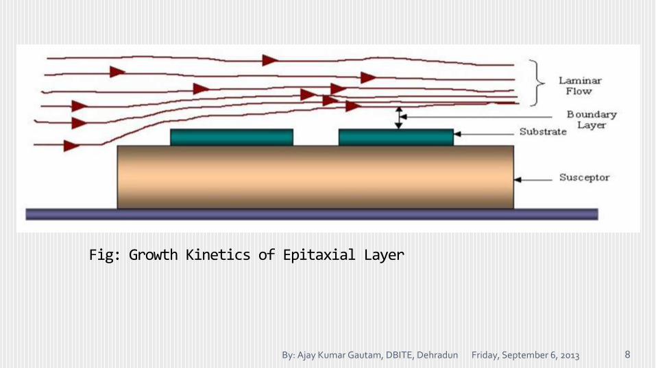
Fig: Growth Kinetics of Epitaxial Layer
Friday, September 6, 2013By: Ajay Kumar Gautam, DBITE, Dehradun 9
The material which we want to deposit is now on the samples.
Samples are already present inside the reactor.
The gas is flowing inside the reactor with a finite velocity.
At the point of contact on the substrate, the velocity is zero.
So, at other places the velocity of the gas is finite in the reactor.
It means, inside the reactor the velocity of the gas at different regions is different.
The velocity of the gas just right next to the first substrate is very low.
It means reactants are not moving very fast.
It means, we have a boundary layer.
So for VPE the width of the boundary layer is very important.
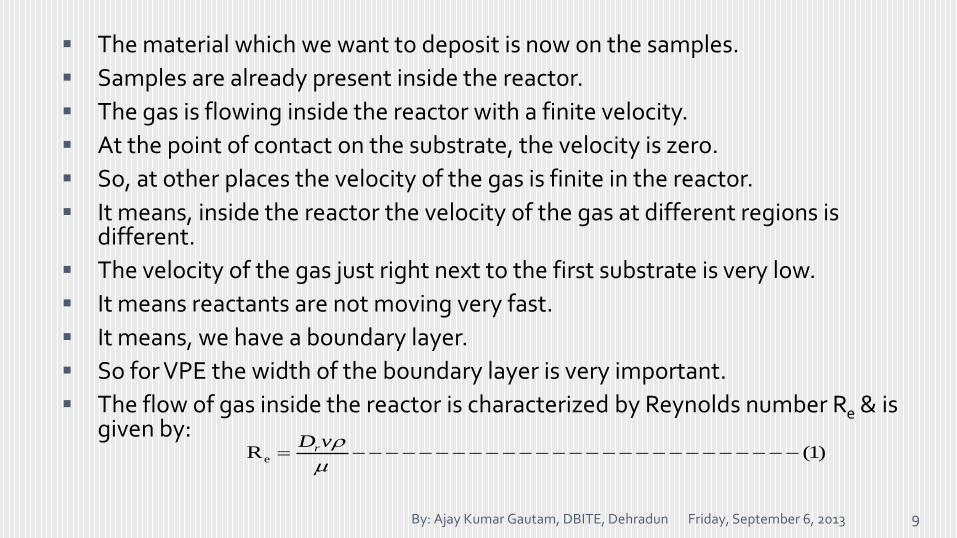
The flow of gas inside the reactor is characterized by Reynolds number Re & is given by:
eR (1)rD v
Friday, September 6, 2013By: Ajay Kumar Gautam, DBITE, Dehradun 10
Dr is Diameter through which the gas is moving. V is velocity of the gas flow. ρ is the density of the gas. µ is the viscosity of the gas.
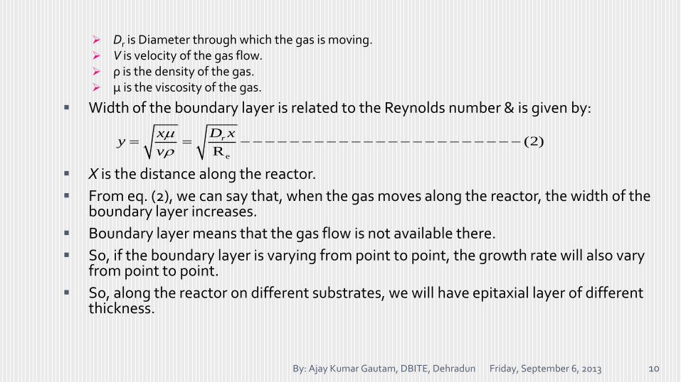
Width of the boundary layer is related to the Reynolds number & is given by:
X is the distance along the reactor.
From eq. (2), we can say that, when the gas moves along the reactor, the width of the boundary layer increases.
Boundary layer means that the gas flow is not available there.
So, if the boundary layer is varying from point to point, the growth rate will also vary from point to point.
So, along the reactor on different substrates, we will have epitaxial layer of different thickness.
e
(2)R
rD xxy
v
Friday, September 6, 2013By: Ajay Kumar Gautam, DBITE, Dehradun 11
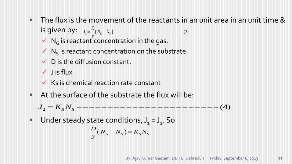
The flux is the movement of the reactants in an unit area in an unit time & is given by:
NG is reactant concentration in the gas.
NS is reactant concentration on the substrate.
D is the diffusion constant.
J is flux
Ks is chemical reaction rate constant
At the surface of the substrate the flux will be:
Under steady state conditions, J1 = J2. So
1 (3)G S
DJ N N
y
2 (4)S SJ K N
G S S S
DN N K N
y
Friday, September 6, 2013By: Ajay Kumar Gautam, DBITE, Dehradun 12
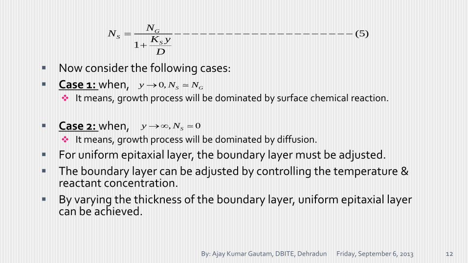
Now consider the following cases:
Case 1: when, It means, growth process will be dominated by surface chemical reaction.
Case 2: when, It means, growth process will be dominated by diffusion.
For uniform epitaxial layer, the boundary layer must be adjusted.
The boundary layer can be adjusted by controlling the temperature & reactant concentration.
By varying the thickness of the boundary layer, uniform epitaxial layer can be achieved.
(5)
1
GS
S
NN
K y
D
0, S Gy N N
, 0Sy N
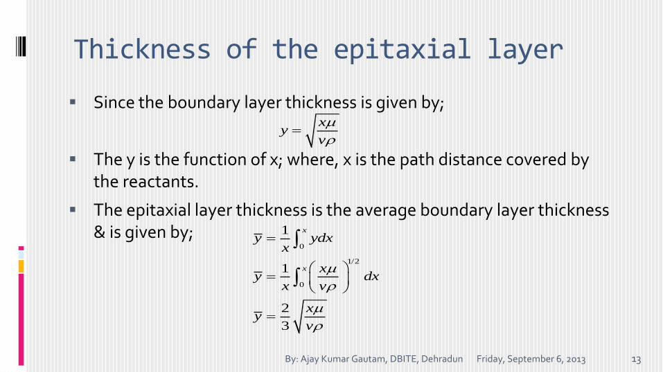
Thickness of the epitaxial layer
Since the boundary layer thickness is given by;
The y is the function of x; where, x is the path distance covered by the reactants.
The epitaxial layer thickness is the average boundary layer thickness & is given by;
Friday, September 6, 2013By: Ajay Kumar Gautam, DBITE, Dehradun 13
xy
v
0
1/2
0
1
1
2
3
x
x
y ydxx
xy dx
x v
xy
v
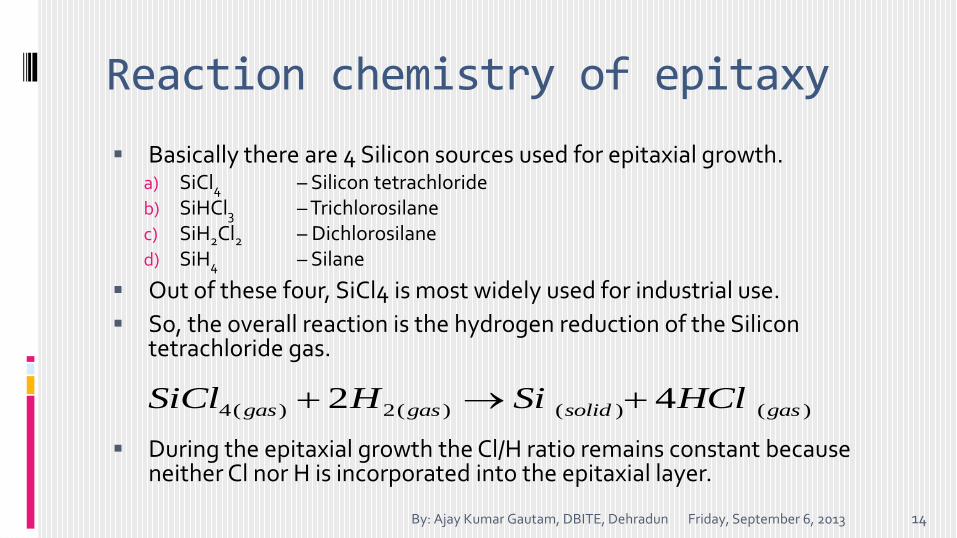
Reaction chemistry of epitaxy
Basically there are 4 Silicon sources used for epitaxial growth.a) SiCl4 – Silicon tetrachlorideb) SiHCl3 – Trichlorosilanec) SiH2Cl2 – Dichlorosilaned) SiH4 – Silane
Out of these four, SiCl4 is most widely used for industrial use.
So, the overall reaction is the hydrogen reduction of the Silicon tetrachloride gas.
During the epitaxial growth the Cl/H ratio remains constant because neither Cl nor H is incorporated into the epitaxial layer.
Friday, September 6, 2013By: Ajay Kumar Gautam, DBITE, Dehradun 14
4( ) 2( ) ( ) ( )2 4gas gas solid gasSiCl H Si HCl
Cont...
The epitaxial layer is growing it means, there is deposition of reactants (Si) from the gases on the surface of the substrate.
The deposition rate is always –ve.
The deposition rate is –ve; it means the concentration of the reactants outside the reactor is larger than that of at the reactor. i.e., NG>NS.
It means reactants are moving from higher concentration region to lower concentration region.
So, epitaxial process takes place because of –ve deposition rate.
Friday, September 6, 2013By: Ajay Kumar Gautam, DBITE, Dehradun 15
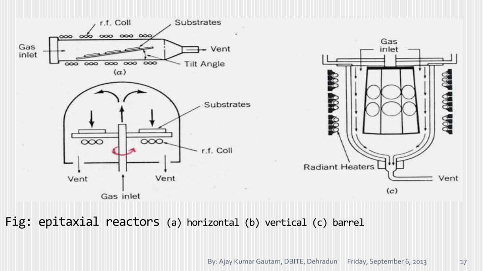
Epitaxial Apparatus
Basically we are having 3 reactors for epitaxial growth.a) Horizontal reactorb) Vertical reactorc) Barrel reactor
In horizontal reactor, we have are having inclined sample holder as shown in fig.
In this kind of reactor, we have parallel gas flow.
In vertical reactor, gas flow is the normal to the surface of the sample.
In vertical reactor, we can’t place much more samples at a time.
For mass production, the barrel reactor is used.
Friday, September 6, 2013By: Ajay Kumar Gautam, DBITE, Dehradun 16
Friday, September 6, 2013By: Ajay Kumar Gautam, DBITE, Dehradun 17
Fig: epitaxial reactors (a) horizontal (b) vertical (c) barrel
Cont...
In this kind of reactor, the reactor the sample holder is a barrel or drum.
In this barrel, we are having small grooves.
In each of the grooves, the samples are placed.
The barrel can be rotate for uniform epitaxial growth.
The flow of the gas is parallel to the surface of the wafer.
In a barrel reactor, lot of samples can be placed in a same time.
Better growth can be achieved by rotating the barrel.
For the epitaxial reactor, there are lot of steps.
Friday, September 6, 2013By: Ajay Kumar Gautam, DBITE, Dehradun 18
Cont...
First step is to filled up the reactor with hydrogen gas.
Initially this hydrogen gas will clean the reactor. So, the hydrogen gas will react with the air & will form water.
After that heating of the reactor is required through RF heaters.
This will convert the water in vaporized form.
After that the vaporized water can be taken out from the gas outlet.
Friday, September 6, 2013By: Ajay Kumar Gautam, DBITE, Dehradun 19
Cont...
Next step is to filled up the reactor with the silicon sources.
Growth process starts at a rate of 0.2 µm/min to 2.o µm/min.
When the epitaxial growth has completed, we need to shut off the power.
Remove the silicon sources & dopants.
Dopants may be n type or p type.
Reactor is cooled upto the ambient temperature.
Since the reactor may consist of some gases, so we need to filled up the reactor with some inert gases.
Usually the inert gas may be nitrogen, so that the reactor may be opened safely.
Friday, September 6, 2013By: Ajay Kumar Gautam, DBITE, Dehradun 20
Autodoping
It is the process of transporting doping atoms from the substrate into the epitaxial layer.
Friday, September 6, 2013By: Ajay Kumar Gautam, DBITE, Dehradun 21
Fig: Auto Doping process in an epitaxial reactor1 – wafer front side 2- wafer back side 3 – other wafer 4 - susceptor
Friday, September 6, 2013By: Ajay Kumar Gautam, DBITE, Dehradun 22
So, in auto doping unintentional dopants are incorporated from the substrate.
This effect is called “auto doping”.
These unintended impurities may come to the wafer from:
1. wafer front side
2. wafer back side
3. other wafer
4. Susceptor
The auto doping can be removed by pre – epitaxial process inside the reactor.
For this HCL etching takes place at 12000 C.
4 24 2HCl Si SiCl H
Low Temperature Epitaxy
Epitaxial growth at low temperature is used to minimize the auto doping effect.
Lower epitaxial growth rate can be achieved even at low temperature.
Molecular Beam Epitaxy (MBE) is the example of low temperature epitaxy.
Friday, September 6, 2013By: Ajay Kumar Gautam, DBITE, Dehradun 23
Molecular Beam Epitaxy
It is physical evaporation process, with no chemical reactions involved in it.
The epitaxial layer, which we will be grown on Si substrate is usually Si in Silicon technology.
The evaporation is done under very high vacuum condition.
The heart of the MBE process is the ultra high vacuum pumping.
After achieving the ultra high vacuum condition, next step is to evaporate the epitaxial species (Si).
Since the Silicon (Si) has very high melting point, so it is very difficult the silicon by thermal heating.
So, evaporation process of silicon is done with electron gun.
Friday, September 6, 2013By: Ajay Kumar Gautam, DBITE, Dehradun 24
Friday, September 6, 2013By: Ajay Kumar Gautam, DBITE, Dehradun 25
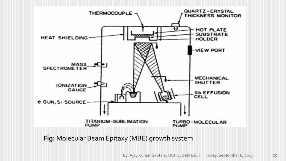
Fig: Molecular Beam Epitaxy (MBE) growth system
Friday, September 6, 2013By: Ajay Kumar Gautam, DBITE, Dehradun 26
The electron beam is focused on the silicon source, after that silicon is evaporated.
In MBE system, we have 2 pumps.
The pumps are used to achieve the ultra high vacuum condition.
Also we have a silicon source.
We have crucible in which the silicon is placed.
e - beam is focused on the silicon source.
From this silicon source, silicon is evaporated from the conical shape.
Effusion cell is used to introduce the dopants.
Effusion cell is the dopant holder, which is heated.
There is a small opening at the mouth of the effusion cell, through which evaporated dopants come out.
We have two shutters, these are controlled by microcontroller.
The shutters are used to control the layer thickness and amount of dopants incorporated in the epitaxial layer.
Friday, September 6, 2013By: Ajay Kumar Gautam, DBITE, Dehradun 27
Sample holder supports the Sil icon substrate.
Additionally we have a heater and thermocouple.
Thermocouple is used to measure the temperature of the substrate.
Substrate temperature is usually kept 400 0 C to 800 0 C.
So, we have the following steps for MBE .
1) Create the ultra high vacuum condition with the help of pumps.
2) Switch on the electron gun in order to evaporate the silicon.
3) Heat the effusion cell in order to incorporate the dopant.
4) Open the shutter at the top of two cones, dopants will be mixed with silicon.
Advantages of MBE over VPE1. Low Temperature Process: because of low temperature
process, the auto doping effect can be minimized from substrate to epitaxial layer.
2. Precise Control of Doping: this is because there is no chemical reaction involved. It is only physical evaporation process. Measured quantity of the dopants can be evaporated.
3. Growth Rate: growth rate can be achieved as small as possible.
4. No Boundary (Stagnant) Layer Problem: there is no boundary problem, so the growth rate is equal for all the substrate.
Friday, September 6, 2013By: Ajay Kumar Gautam, DBITE, Dehradun 28
Disadvantages of MBE over VPE
1. Very costly equipment
2. Very complicated equipment
Friday, September 6, 2013By: Ajay Kumar Gautam, DBITE, Dehradun 29
Module 2
Friday, September 6, 2013By: Ajay Kumar Gautam, DBITE, Dehradun 30
DIFFUSION PROCESS
Diffusion Model of Solids
Process by which controlled amount of impurities are introduced into the semiconductor.
Impurities atoms moves inside the silicon crystal because a concentration gradient exists inside the crystal.
Under this concentration gradient, impurity atoms move inside the crystal.
If the crystal has lot of vacancies, then its very easy for impurity atoms to go inside and occupy the vacant space.
Diffusion process may be divided into 3 categories.1. Substitution2. Interstitial3. Interstitialcy
Friday, September 6, 2013By: Ajay Kumar Gautam, DBITE, Dehradun 31
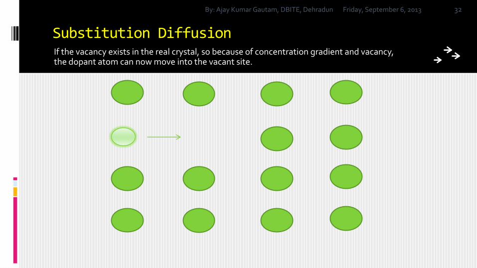
Substitution DiffusionIf the vacancy exists in the real crystal, so because of concentration gradient and vacancy, the dopant atom can now move into the vacant site.
Friday, September 6, 2013By: Ajay Kumar Gautam, DBITE, Dehradun 32
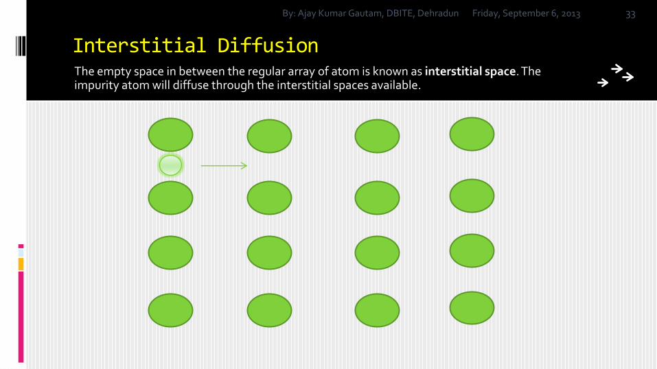
Interstitial DiffusionThe empty space in between the regular array of atom is known as interstitial space. The impurity atom will diffuse through the interstitial spaces available.
Friday, September 6, 2013By: Ajay Kumar Gautam, DBITE, Dehradun 33
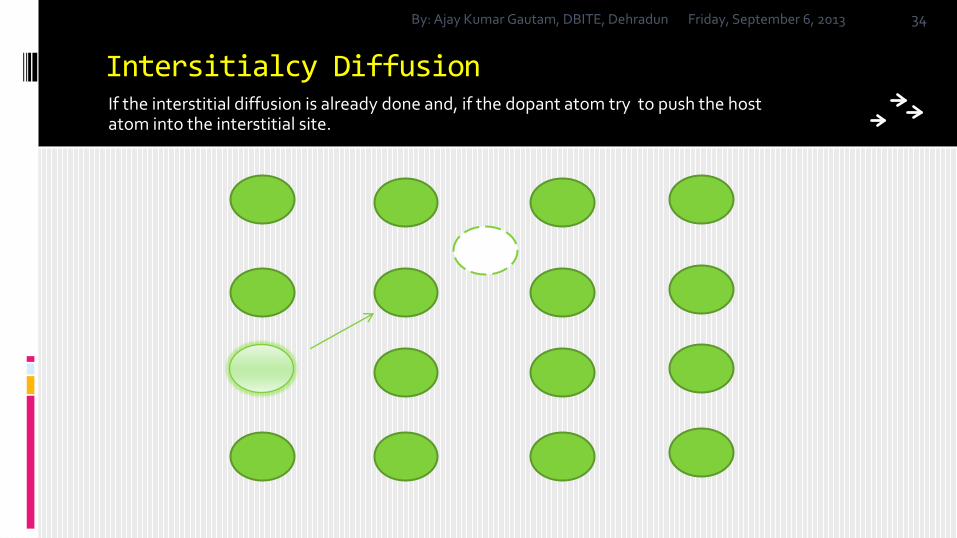
Intersitialcy DiffusionIf the interstitial diffusion is already done and, if the dopant atom try to push the host atom into the interstitial site.
Friday, September 6, 2013By: Ajay Kumar Gautam, DBITE, Dehradun 34
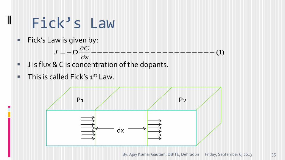
Fick’s Law Fick’s Law is given by:
J is flux & C is concentration of the dopants.
This is called Fick’s 1st Law.
Friday, September 6, 2013By: Ajay Kumar Gautam, DBITE, Dehradun 35
(1)C
J Dx
P1 P2
dx
Friday, September 6, 2013By: Ajay Kumar Gautam, DBITE, Dehradun 36
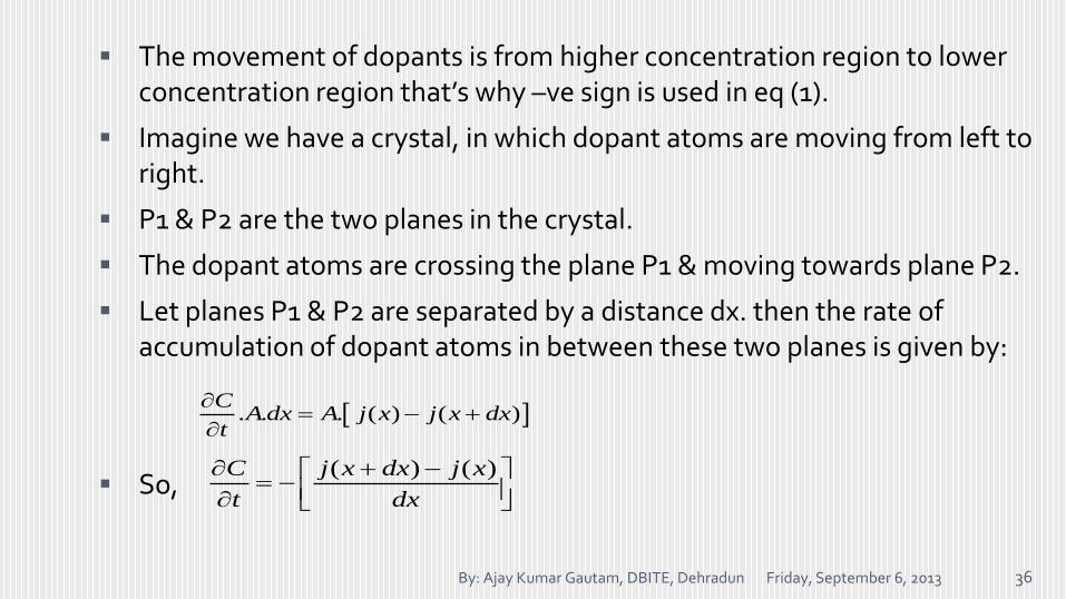
The movement of dopants is from higher concentration region to lower concentration region that’s why –ve sign is used in eq (1).
Imagine we have a crystal, in which dopant atoms are moving from left to right.
P1 & P2 are the two planes in the crystal.
The dopant atoms are crossing the plane P1 & moving towards plane P2.
Let planes P1 & P2 are separated by a distance dx. then the rate of accumulation of dopant atoms in between these two planes is given by:
So,
. . . ( ) ( )C
A dx A j x j x dxt
( ) ( )C j x dx j x
t dx
Friday, September 6, 2013By: Ajay Kumar Gautam, DBITE, Dehradun 37
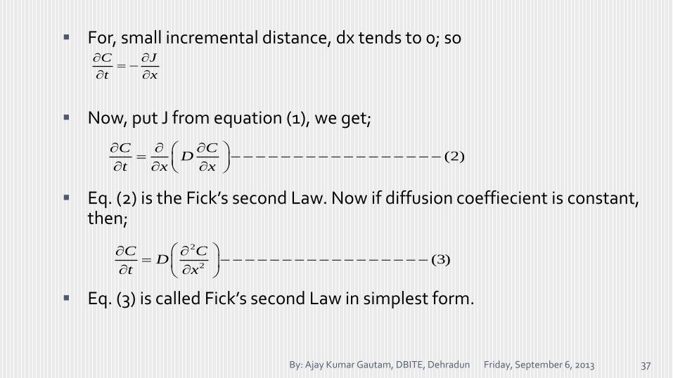
For, small incremental distance, dx tends to 0; so
Now, put J from equation (1), we get;
Eq. (2) is the Fick’s second Law. Now if diffusion coeffiecient is constant, then;
Eq. (3) is called Fick’s second Law in simplest form.
C J
t x
2
2(3)
C CD
t x
(2)C C
Dt x x
Solution of Fick’s Law
The Fick’s Law can be solved in the following ways. Let D is constant i.e., we have Constant Diffusivities.
Friday, September 6, 2013By: Ajay Kumar Gautam, DBITE, Dehradun 38
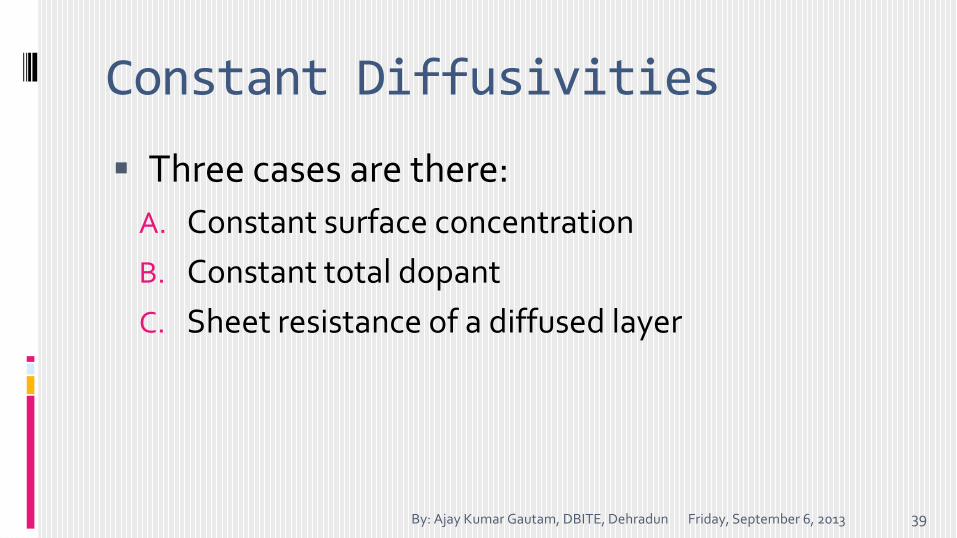
Constant Diffusivities
Three cases are there:
A. Constant surface concentration
B. Constant total dopant
C. Sheet resistance of a diffused layer
Friday, September 6, 2013By: Ajay Kumar Gautam, DBITE, Dehradun 39
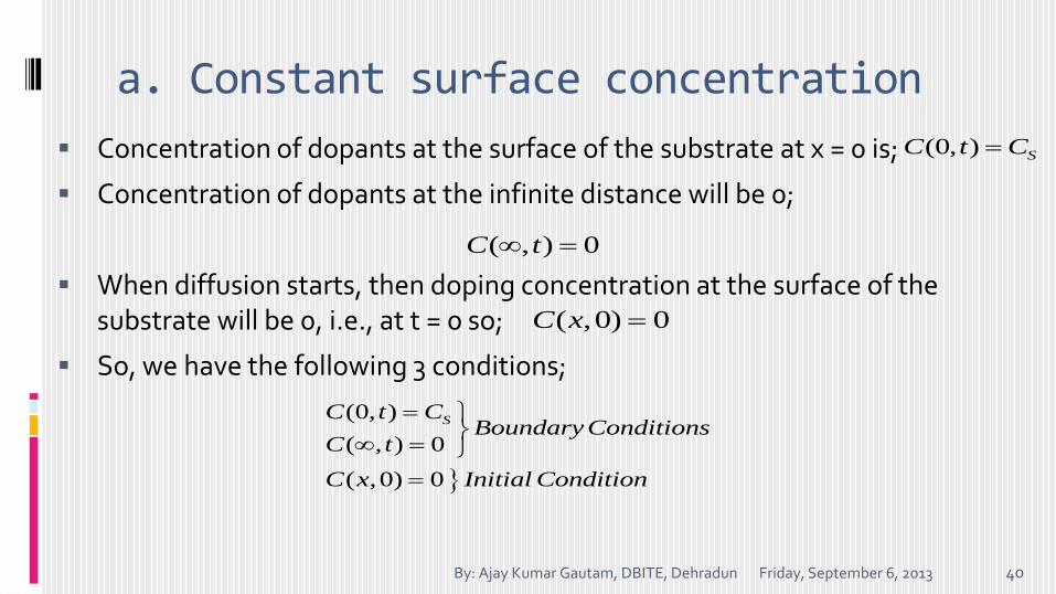
a. Constant surface concentration
Concentration of dopants at the surface of the substrate at x = 0 is;
Concentration of dopants at the infinite distance will be 0;
When diffusion starts, then doping concentration at the surface of the substrate will be 0, i.e., at t = 0 so;
So, we have the following 3 conditions;
Friday, September 6, 2013By: Ajay Kumar Gautam, DBITE, Dehradun 40
(0, ) SC t C
( , ) 0C t
( ,0) 0C x
(0, )
( , ) 0
( ,0) 0
SC t CBoundaryConditions
C t
C x Initial Condition
Friday, September 6, 2013By: Ajay Kumar Gautam, DBITE, Dehradun 41
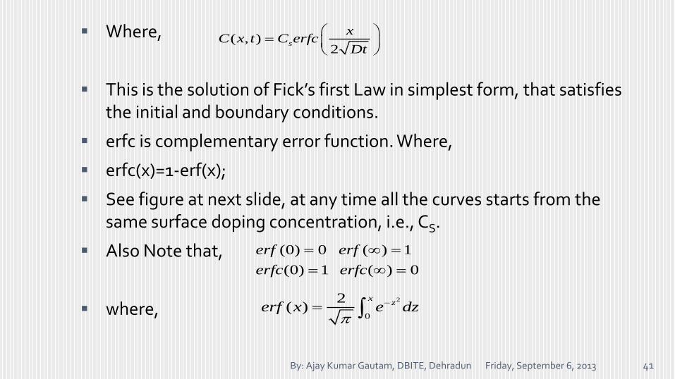
Where,
This is the solution of Fick’s first Law in simplest form, that satisfies the initial and boundary conditions.
erfc is complementary error function. Where,
erfc(x)=1-erf(x);
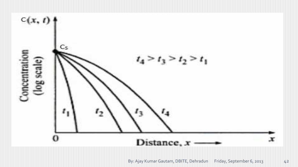
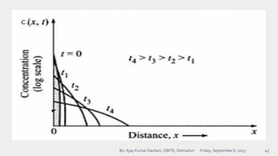
See figure at next slide, at any time all the curves starts from the same surface doping concentration, i.e., CS.
Also Note that,
where,
( , )2
s
xC x t C erfc
Dt
(0) 0 ( ) 1
(0) 1 ( ) 0
erf erf
erfc erfc
2
0
2( )
xzerf x e dz
Friday, September 6, 2013By: Ajay Kumar Gautam, DBITE, Dehradun 42
Friday, September 6, 2013By: Ajay Kumar Gautam, DBITE, Dehradun 43
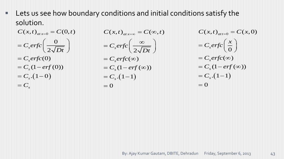
Lets us see how boundary conditions and initial conditions satisfy the solution.
0( , ) (0, )
0
2
(0)
(1 (0))
. 1 0
at x
s
s
s
s
s
C x t C t
C erfcDt
C erfc
C erf
C
C
( , ) ( , )
2
( )
(1 ( ))
. 1 1
0
at x
s
s
s
s
C x t C t
C erfcDt
C erfc
C erf
C
0( , ) ( ,0)
0
( )
(1 ( ))
. 1 1
0
at t
s
s
s
s
C x t C x
xC erfc
C erfc
C erf
C
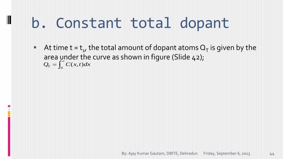
b. Constant total dopant
At time t = t1, the total amount of dopant atoms QT is given by the area under the curve as shown in figure (Slide 42);
Friday, September 6, 2013By: Ajay Kumar Gautam, DBITE, Dehradun 44
0( , )TQ C x t dx
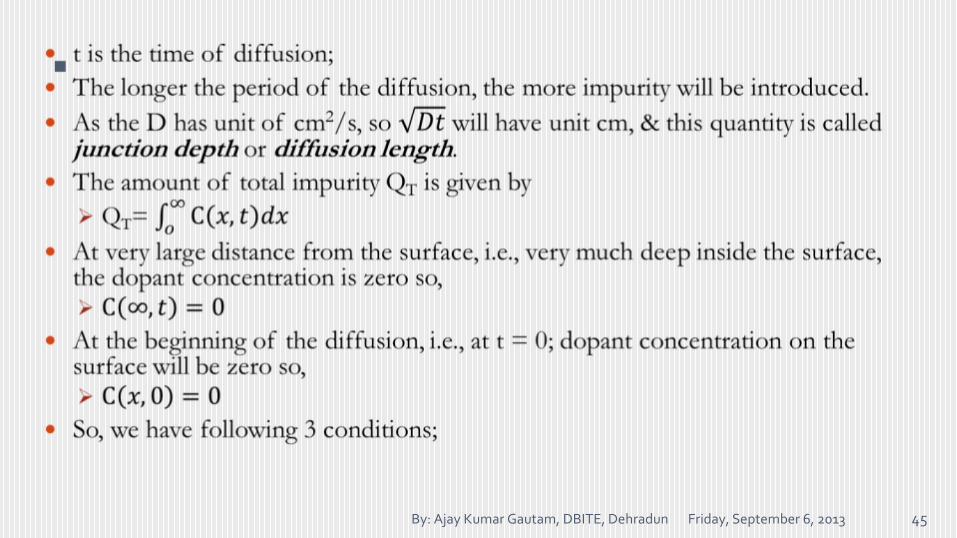
Friday, September 6, 2013By: Ajay Kumar Gautam, DBITE, Dehradun 45
Friday, September 6, 2013By: Ajay Kumar Gautam, DBITE, Dehradun 46
2
( , ) exp4
TQ xC x t
DtDt
0
( , ) 0
( , )
( ,0) 0
x
T
C tBoundaryConditions
C x t dx Q
C x Initial Contition
Friday, September 6, 2013By: Ajay Kumar Gautam, DBITE, Dehradun 47
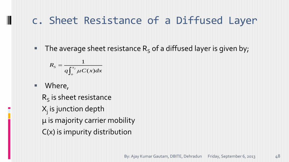
c. Sheet Resistance of a Diffused Layer
The average sheet resistance RS of a diffused layer is given by;
Where,
RS is sheet resistance
Xj is junction depth
µ is majority carrier mobility
C(x) is impurity distribution
Friday, September 6, 2013By: Ajay Kumar Gautam, DBITE, Dehradun 48
1
( )j
S x
o
Rq C x dx
Diffusion Parameters Measurements Schemes
Four point Probe Method
Vander Pauw Technique
Friday, September 6, 2013By: Ajay Kumar Gautam, DBITE, Dehradun 49
Four Probe Point Method
Already discussed during crystal growth
Friday, September 6, 2013By: Ajay Kumar Gautam, DBITE, Dehradun 50
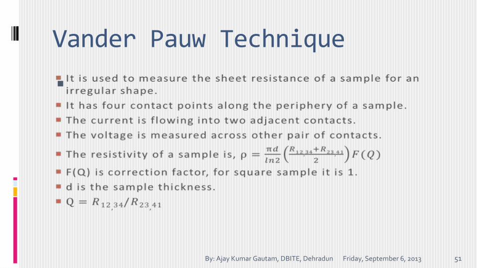
Vander Pauw Technique
Friday, September 6, 2013By: Ajay Kumar Gautam, DBITE, Dehradun 51
Module 3
Friday, September 6, 2013By: Ajay Kumar Gautam, DBITE, Dehradun 52
ION IMPLANTATION
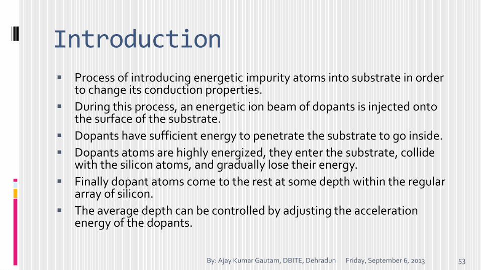
Introduction
Process of introducing energetic impurity atoms into substrate in order to change its conduction properties.
During this process, an energetic ion beam of dopants is injected onto the surface of the substrate.
Dopants have sufficient energy to penetrate the substrate to go inside.
Dopants atoms are highly energized, they enter the substrate, collide with the silicon atoms, and gradually lose their energy.
Finally dopant atoms come to the rest at some depth within the regular array of silicon.
The average depth can be controlled by adjusting the acceleration energy of the dopants.
Friday, September 6, 2013By: Ajay Kumar Gautam, DBITE, Dehradun 53
Advantages of Ion implantation
1. Less prone to contamination
2. Better control of total impurity
3. Low temperature process
4. Better flexibility
Friday, September 6, 2013By: Ajay Kumar Gautam, DBITE, Dehradun 54
1. Less Prone to Contamination
Major consideration in the diffusion are contamination.
For diffusion boron & phosphorus, same furnace can’t be used.
Because inside the furnace, there will be lot of contamination.
Also same push rod can’t be used for diffusion.
While, in ion-implantation is much less prone to contamination.
The same system can be used to implant various dopants.
Ion-implantation is done under high vacuum condition.
The high vacuum system is much more clean.
Because in order to create high vacuum condition, the contamination are pumped out.
Friday, September 6, 2013By: Ajay Kumar Gautam, DBITE, Dehradun 55
2. Better Control of Total Impurity
In Diffusion, the control of doping profile is usually within 5% to 10% of the predicted value.
It is because ambient conditions can’t adjusted accurately.
In ion implantation, the control of doping profile is within -10% to +10%.
It is because, in ion implantation, an ion beam is directed on to the surface of the substrate.
So, the doors of the ion beam can be adjusted by simply adjusting the ion beam flow.
Friday, September 6, 2013By: Ajay Kumar Gautam, DBITE, Dehradun 56
3. Low Temperature Process
Diffusion is a high temperature process (800 0C – 1200 0C).
So, for diffusion, SiO2 can be used as mask.
While the ion implantation is room temperature process.
But in ion implantation photoresist only can be used as mask.
So, the thermal budget is reduced in ion implantation.
Friday, September 6, 2013By: Ajay Kumar Gautam, DBITE, Dehradun 57
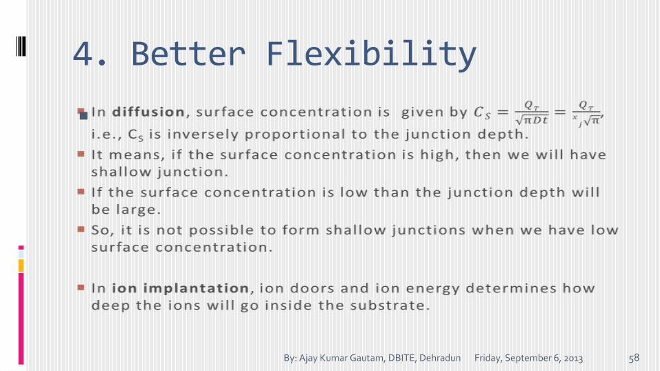
4. Better Flexibility
Friday, September 6, 2013By: Ajay Kumar Gautam, DBITE, Dehradun 58
Disadvantages of Ion Implantation
The equipment is expansive.
This is much more complicated technique.
Ion implantation creates damage to the semiconductor substrate.
Friday, September 6, 2013By: Ajay Kumar Gautam, DBITE, Dehradun 59
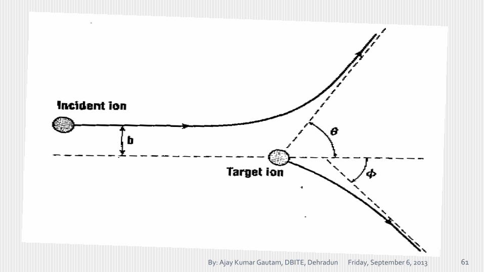
Scattering Phenomenon
Since, in ion implantation system, ions must have highly energized in order to penetrate the substrate.
The ion may collide with the target atom in the regular array of silicon & may displace it.
The target atom is initially at rest.
Let incident ion has incident velocity v and an impact parameter b as shown in figure.
As the incident ion has some energy, so when it will penetrate onto the silicon substrate, it will come on rest and will loose it energy gradually.
Friday, September 6, 2013By: Ajay Kumar Gautam, DBITE, Dehradun 60
Friday, September 6, 2013By: Ajay Kumar Gautam, DBITE, Dehradun 61
Range Theory
Since, during the ion implantation process, an energetic ion beam of dopants is injected onto the surface of the substrate.
Dopants have sufficient energy so as to penetrate the substrate.
Once the atoms go inside the substrate, they starts to loose their energy gradually.
The process of loosing their energy can be controlled by colliding with the lattice atom.
If dopants atoms have sufficient energy, then they can displace the lattice atom towards interstitial site or substitution site.
This is called Nuclear Stopping.
Friday, September 6, 2013By: Ajay Kumar Gautam, DBITE, Dehradun 62
Cond...
So this collision of dopant atoms with lattice atoms create defects.
The ion beam supplies energy to the bounded electrons.
This is called Electronic Stopping.
So, the ion beam is loosing energy by two processes, i.e., Nuclear Stopping & Electronic Stopping.
The Range R is the distance traversed during which the ion energy has fallen from its initial energy E0 to zero.
Friday, September 6, 2013By: Ajay Kumar Gautam, DBITE, Dehradun 63
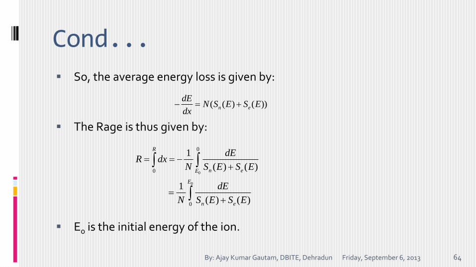
Cond...
So, the average energy loss is given by:
The Rage is thus given by:
E0 is the initial energy of the ion.
Friday, September 6, 2013By: Ajay Kumar Gautam, DBITE, Dehradun 64
0
0
0
0
0
1
( ) ( )
1
( ) ( )
R
n eE
E
n e
dER dx
N S E S E
dE
N S E S E
( ( ) ( ))n e
dEN S E S E
dx
Implantation Damage
During ion implantation, the energetic ions makes many collisions with the lattice atoms before coming to rest.
When sufficient energy is transferred to the lattice, many of its atoms are displaced.
Let we have a single energetic ion as it moves through the substrate & makes collisions with the target atoms.
Let Ed, is the energy required to displace the target atom.
If a lattice atom receives energy less than Ed, it will not be displaced.
Similarly, if incident atom ion collide with lattice atom with energy less than Ed, then no atom will be displaced.
So, incident ion must have an energy of 2Ed.
Friday, September 6, 2013By: Ajay Kumar Gautam, DBITE, Dehradun 65
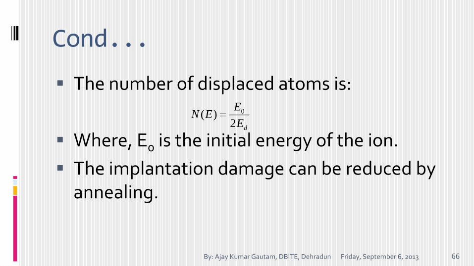
Cond...
The number of displaced atoms is:
Where, E0 is the initial energy of the ion.
The implantation damage can be reduced by annealing.
Friday, September 6, 2013By: Ajay Kumar Gautam, DBITE, Dehradun 66
0( )2 d
EN E
E
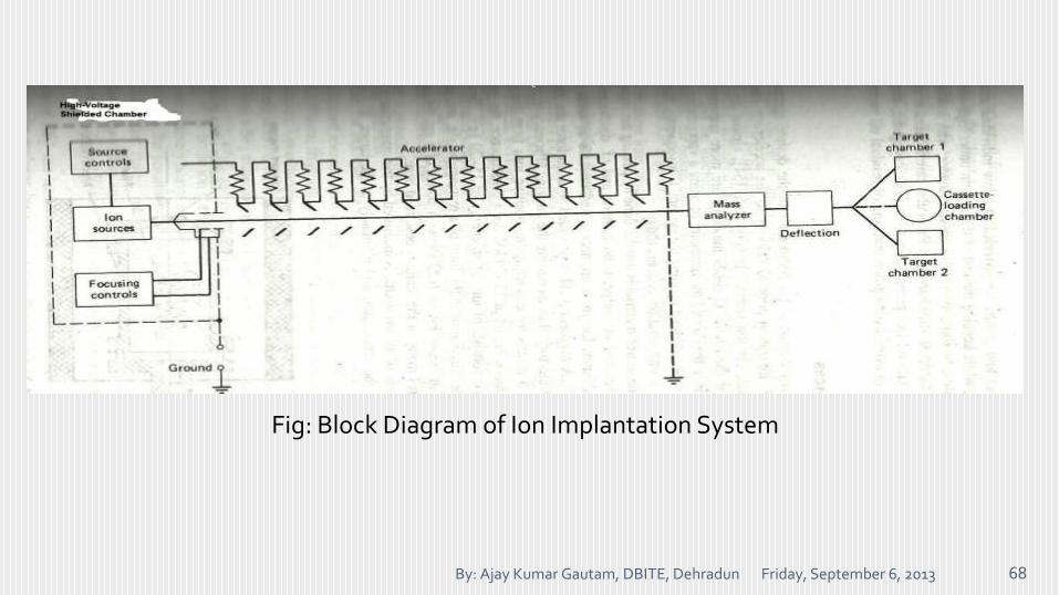
Ion-Implantation Systems
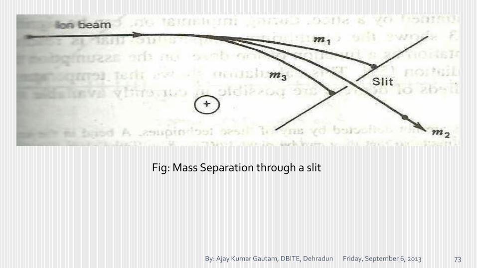
There are two key parameters for ion implants: 1. Ion energy – which determines the penetration depth & 2. ion current – which determines the implantation time.
The basic feature of ion implantation system are – ion source & acceleration of high energy.
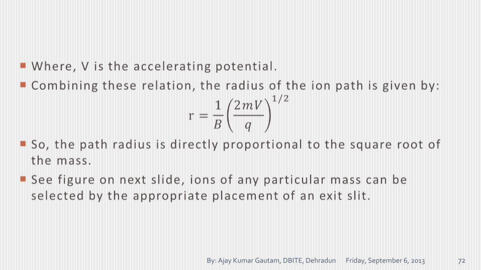
Mass analyzer is used to select the single ion.
All the ion sources, including their power supplies and control elements are controlled by remote.
Rest of the system is kept on ground potential.
Separate valves and pumps are provided in order to maintain the system under high vacuum condition at all the times.
The cassette loader is required to handle the substrate.
Friday, September 6, 2013By: Ajay Kumar Gautam, DBITE, Dehradun 67
Friday, September 6, 2013By: Ajay Kumar Gautam, DBITE, Dehradun 68
Fig: Block Diagram of Ion Implantation System
Friday, September 6, 2013By: Ajay Kumar Gautam, DBITE, Dehradun 69
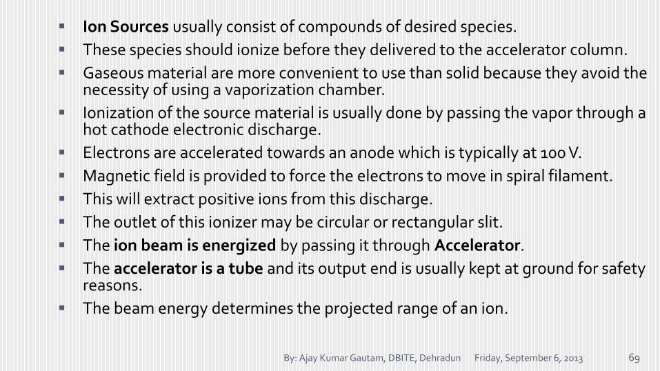
Ion Sources usually consist of compounds of desired species.
These species should ionize before they delivered to the accelerator column.
Gaseous material are more convenient to use than solid because they avoid the necessity of using a vaporization chamber.
Ionization of the source material is usually done by passing the vapor through a hot cathode electronic discharge.
Electrons are accelerated towards an anode which is typically at 100 V.
Magnetic field is provided to force the electrons to move in spiral filament.
This will extract positive ions from this discharge.
The outlet of this ionizer may be circular or rectangular slit.
The ion beam is energized by passing it through Accelerator.
The accelerator is a tube and its output end is usually kept at ground for safety reasons.
The beam energy determines the projected range of an ion.
Friday, September 6, 2013By: Ajay Kumar Gautam, DBITE, Dehradun 70
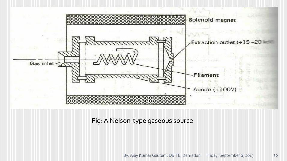
Fig: A Nelson-type gaseous source
Friday, September 6, 2013By: Ajay Kumar Gautam, DBITE, Dehradun 71
Friday, September 6, 2013By: Ajay Kumar Gautam, DBITE, Dehradun 72
Friday, September 6, 2013By: Ajay Kumar Gautam, DBITE, Dehradun 73
Fig: Mass Separation through a slit
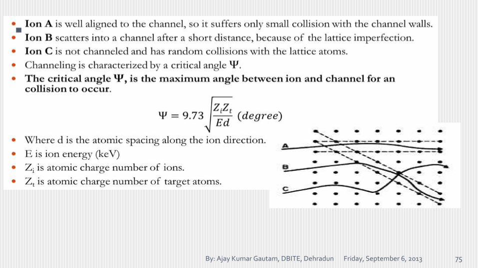
Channeling The substrate has crystalline structure with regular
arrangements of atoms.
The atoms rows may have open spaces through which ions can travel without significant scattering.
The figure shows three ions entering a simple cubic lattice.
Friday, September 6, 2013By: Ajay Kumar Gautam, DBITE, Dehradun 74
Friday, September 6, 2013By: Ajay Kumar Gautam, DBITE, Dehradun 75
Annealing
The dopant atoms are introduced into a semiconductor in order to change its electrical properties.
During ion implantation atoms may displace and may create defects.
Annealing is required to repair the lattice damage and put dopant atoms on substitutional sites where they will be electrically active.
Friday, September 6, 2013By: Ajay Kumar Gautam, DBITE, Dehradun 76
Cond...
The thermal anneal cycles are usually 15-30 minutes in duration.
During the anneal phase, displaced atoms tend to move in order to repair damages.
Anneal process takes place at temperature of 1200 0C.
Friday, September 6, 2013By: Ajay Kumar Gautam, DBITE, Dehradun 77
Cond...
Rapid Thermal Annealing: The process usually takes place at a temperature of 12000C.
The process of annealing takes place in order to dissolve the defects i.e., damages.
The lattice atoms have the energy of 5 keV.
These are associated with the diffusion of self-interstitials.
Friday, September 6, 2013By: Ajay Kumar Gautam, DBITE, Dehradun 78
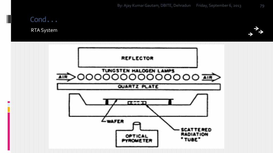
Cond...RTA System
Friday, September 6, 2013By: Ajay Kumar Gautam, DBITE, Dehradun 79
Cond...
A typical water cooled RTA system with tungsten halogen lamps is shown in figure.
The absorption of radiant heat is directly related to the free carrier concentration.
So, the heating rate for heavily doped material is more rapid than lightly doped materials.
Friday, September 6, 2013By: Ajay Kumar Gautam, DBITE, Dehradun 80
Cond...
So, the temperature monitoring is very much necessary in this system.
The optical pyrometers and thermocouples are used for this purpose.
Friday, September 6, 2013By: Ajay Kumar Gautam, DBITE, Dehradun 81
Review questions
1. What is Epitaxy? Discuss Molecular Beam Epitaxy technique in brief. What are the advantages of MBE over VPE?
2. Explain the kinetics of Epitaxy. Calculate epitaxial layer thickness.
3. What are the sources of silicon in VPE?
4. Why epitaxial layer of Si is necessary to grow? What are the functions of this layer in IC?
5. What is Autodoping? What are the disadvantages of Autodoping? How it can be minimized?
Friday, September 6, 2013By: Ajay Kumar Gautam, DBITE, Dehradun 82
Friday, September 6, 2013By: Ajay Kumar Gautam, DBITE, Dehradun 83
6. Derive the diffusion equation. How the depth of diffusion is controlled during diffusion process? Give the solution of Fick’s Law?
7. Describe a typical ion implanter.8. What are the advantages of ion implantation?9. What is Ion Implantation? Explain the process with a
neat diagram. 10. What do you mean by Annealing? Why it is required in
IC fabrication process?11. Compare ion implantation process with diffusion.
References
1. VLSI Technology/S. M. SZE/2nd Ed./TMH
2. VLSI Fabrication Principles Silicon and Gallium Arsenide/Sorab K. Gandhi/2nd Ed./Wiley
3. The Science and Engineering of Microelectronic Fabrication/S. A. Campbell/2nd Ed./Oxford
4. Silicon VLSI Technology – Fundamentals, Practice and Modeling/J. D. Plummer, M. D. Deal & P. D. Griffin/1st
Ed./Pearson
5. Semiconductor Devices: Physics & Technology/2nd Ed./S. M. Sze/Wiley
Friday, September 6, 2013By: Ajay Kumar Gautam, DBITE, Dehradun 84