Embed Size (px)
Citation preview
MODEL : AIT02ZPFC-01NL
March 2016 Rev02 SH 1 /17
Technical Reference Note
AIT02ZPFC Power Factor
Correction Series
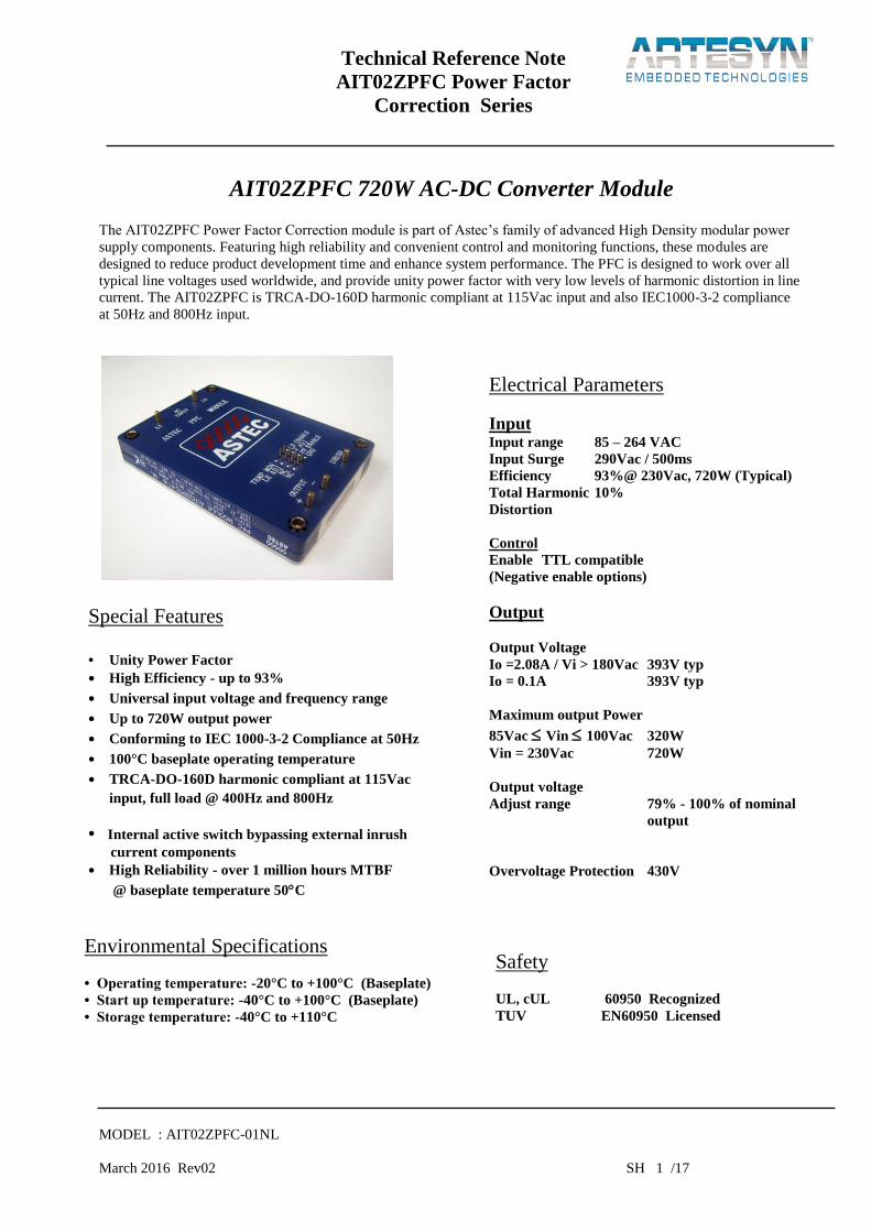
AIT02ZPFC 720W AC-DC Converter Module The AIT02ZPFC Power Factor Correction module is part of Astec’s family of advanced High Density modular power
supply components. Featuring high reliability and convenient control and monitoring functions, these modules are
designed to reduce product development time and enhance system performance. The PFC is designed to work over all
typical line voltages used worldwide, and provide unity power factor with very low levels of harmonic distortion in line
current. The AIT02ZPFC is TRCA-DO-160D harmonic compliant at 115Vac input and also IEC1000-3-2 compliance
at 50Hz and 800Hz input.
Environmental Specifications
• Operating temperature: -20°C to +100°C (Baseplate)
• Start up temperature: -40°C to +100°C (Baseplate)
• Storage temperature: -40°C to +110°C
Electrical Parameters
Input Input range 85 – 264 VAC
Input Surge 290Vac / 500ms
Efficiency 93%@ 230Vac, 720W (Typical)
Total Harmonic 10%
Distortion
Control
Enable TTL compatible
(Negative enable options)
Output
Output Voltage
Io =2.08A / Vi > 180Vac 393V typ
Io = 0.1A 393V typ
Maximum output Power
85Vac Vin 100Vac 320W
Vin = 230Vac 720W
Output voltage
Adjust range 79% - 100% of nominal
output
Overvoltage Protection 430V
Special Features
• Unity Power Factor
• High Efficiency - up to 93%
• Universal input voltage and frequency range
• Up to 720W output power
• Conforming to IEC 1000-3-2 Compliance at 50Hz
• 100°C baseplate operating temperature
• TRCA-DO-160D harmonic compliant at 115Vac
input, full load @ 400Hz and 800Hz
• Internal active switch bypassing external inrush
current components
• High Reliability - over 1 million hours MTBF
@ baseplate temperature 50C
Safety
UL, cUL 60950 Recognized
TUV EN60950 Licensed
MODEL : AIT02ZPFC-01NL
March 2016 Rev02 SH 2 /17
Technical Reference Note
AIT02ZPFC Power Factor
Correction Series
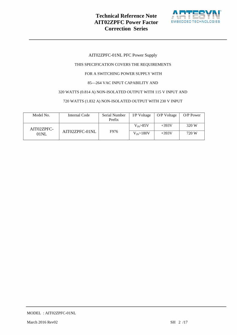
AIT02ZPFC-01NL PFC Power Supply
THIS SPECIFICATION COVERS THE REQUIREMENTS
FOR A SWITCHING POWER SUPPLY WITH
85---264 VAC INPUT CAPABILITY AND
320 WATTS (0.814 A) NON-ISOLATED OUTPUT WITH 115 V INPUT AND
720 WATTS (1.832 A) NON-ISOLATED OUTPUT WITH 230 V INPUT
Model No. Internal Code Serial Number
Prefix
I/P Voltage O/P Voltage O/P Power
AIT02ZPFC-
01NL AIT02ZPFC-01NL F976
VIN>85V +393V 320 W
VIN>180V +393V 720 W
MODEL : AIT02ZPFC-01NL
March 2016 Rev02 SH 3 /17
Technical Reference Note
AIT02ZPFC Power Factor
Correction Series
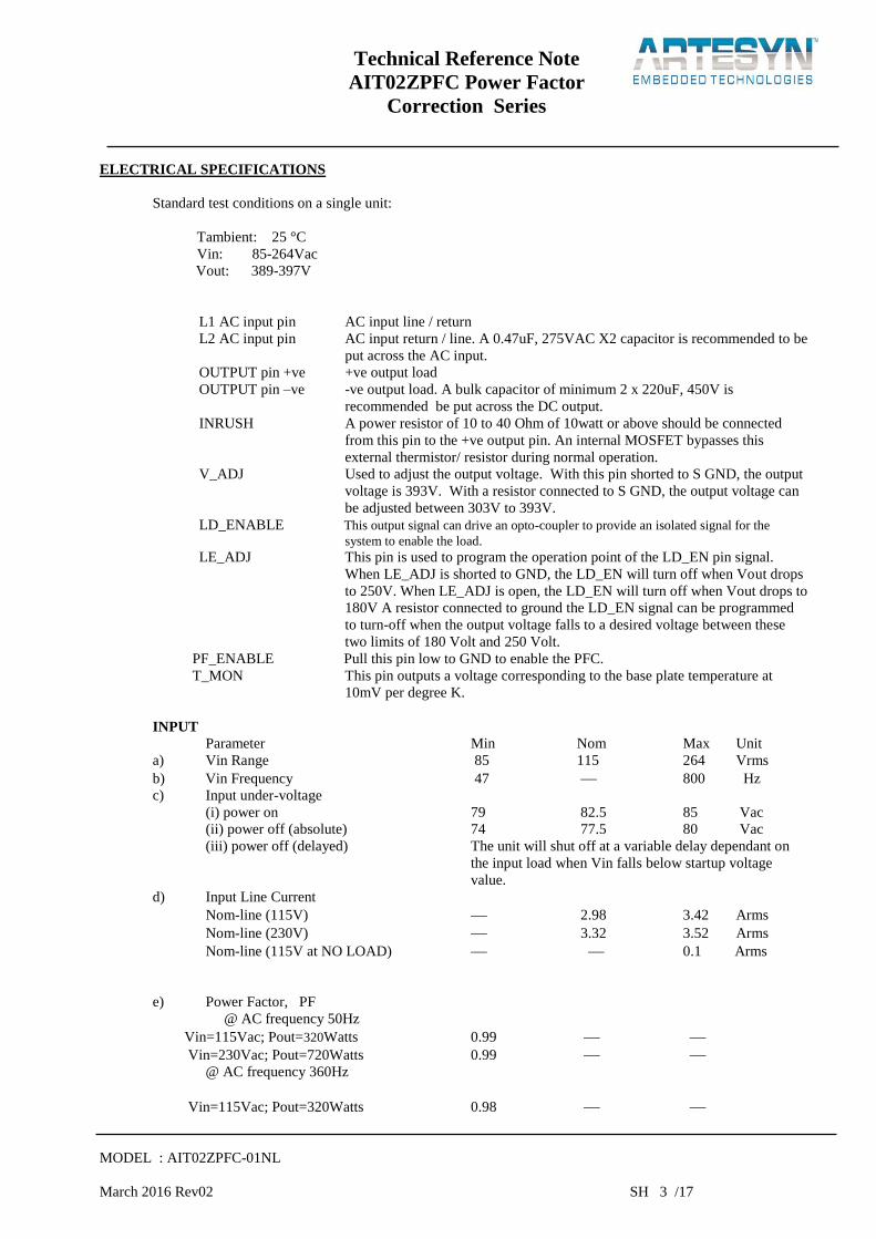
ELECTRICAL SPECIFICATIONS
Standard test conditions on a single unit:
Tambient: 25 °C
Vin: 85-264Vac
Vout: 389-397V
L1 AC input pin AC input line / return
L2 AC input pin AC input return / line. A 0.47uF, 275VAC X2 capacitor is recommended to be
put across the AC input.
OUTPUT pin +ve +ve output load
OUTPUT pin –ve -ve output load. A bulk capacitor of minimum 2 x 220uF, 450V is
recommended be put across the DC output.
INRUSH A power resistor of 10 to 40 Ohm of 10watt or above should be connected
from this pin to the +ve output pin. An internal MOSFET bypasses this
external thermistor/ resistor during normal operation.
V_ADJ Used to adjust the output voltage. With this pin shorted to S GND, the output
voltage is 393V. With a resistor connected to S GND, the output voltage can
be adjusted between 303V to 393V.
LD_ENABLE This output signal can drive an opto-coupler to provide an isolated signal for the
system to enable the load. LE_ADJ This pin is used to program the operation point of the LD_EN pin signal.
When LE_ADJ is shorted to GND, the LD_EN will turn off when Vout drops
to 250V. When LE_ADJ is open, the LD_EN will turn off when Vout drops to
180V A resistor connected to ground the LD_EN signal can be programmed
to turn-off when the output voltage falls to a desired voltage between these
two limits of 180 Volt and 250 Volt.
PF_ENABLE Pull this pin low to GND to enable the PFC.
T_MON This pin outputs a voltage corresponding to the base plate temperature at
10mV per degree K.
INPUT
Parameter Min Nom Max Unit
a) Vin Range 85 115 264 Vrms
b) Vin Frequency 47 800 Hz
c) Input under-voltage
(i) power on 79 82.5 85 Vac
(ii) power off (absolute) 74 77.5 80 Vac
(iii) power off (delayed) The unit will shut off at a variable delay dependant on
the input load when Vin falls below startup voltage
value.
d) Input Line Current
Nom-line (115V) 2.98 3.42 Arms
Nom-line (230V) 3.32 3.52 Arms
Nom-line (115V at NO LOAD) 0.1 Arms
e) Power Factor, PF
@ AC frequency 50Hz
Vin=115Vac; Pout=320Watts 0.99
Vin=230Vac; Pout=720Watts 0.99
@ AC frequency 360Hz
Vin=115Vac; Pout=320Watts 0.98
MODEL : AIT02ZPFC-01NL
March 2016 Rev02 SH 4 /17
Technical Reference Note
AIT02ZPFC Power Factor
Correction Series
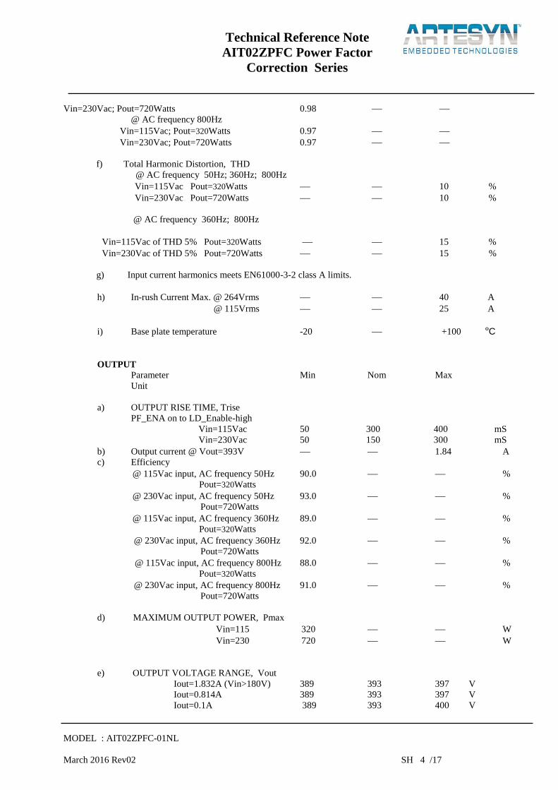
Vin=230Vac; Pout=720Watts 0.98
@ AC frequency 800Hz
Vin=115Vac; Pout=320Watts 0.97
Vin=230Vac; Pout=720Watts 0.97
f) Total Harmonic Distortion, THD
@ AC frequency 50Hz; 360Hz; 800Hz
Vin=115Vac Pout=320Watts 10 %
Vin=230Vac Pout=720Watts 10 %
@ AC frequency 360Hz; 800Hz
Vin=115Vac of THD 5% Pout=320Watts 15 %
Vin=230Vac of THD 5% Pout=720Watts 15 %
g) Input current harmonics meets EN61000-3-2 class A limits.
h) In-rush Current Max. @ 264Vrms 40 A
@ 115Vrms 25 A
i) Base plate temperature -20 +100 ºC
OUTPUT
Parameter Min Nom Max
Unit
a) OUTPUT RISE TIME, Trise
PF_ENA on to LD_Enable-high
Vin=115Vac 50 300 400 mS
Vin=230Vac 50 150 300 mS
b) Output current @ Vout=393V 1.84 A
c) Efficiency
@ 115Vac input, AC frequency 50Hz 90.0 %
Pout=320Watts
@ 230Vac input, AC frequency 50Hz 93.0 %
Pout=720Watts
@ 115Vac input, AC frequency 360Hz 89.0 %
Pout=320Watts
@ 230Vac input, AC frequency 360Hz 92.0 %
Pout=720Watts
@ 115Vac input, AC frequency 800Hz 88.0 %
Pout=320Watts
@ 230Vac input, AC frequency 800Hz 91.0 %
Pout=720Watts
d) MAXIMUM OUTPUT POWER, Pmax
Vin=115 320 W
Vin=230 720 W
e) OUTPUT VOLTAGE RANGE, Vout
Iout=1.832A (Vin>180V) 389 393 397 V
Iout=0.814A 389 393 397 V
Iout=0.1A 389 393 400 V
MODEL : AIT02ZPFC-01NL
March 2016 Rev02 SH 5 /17
Technical Reference Note
AIT02ZPFC Power Factor
Correction Series
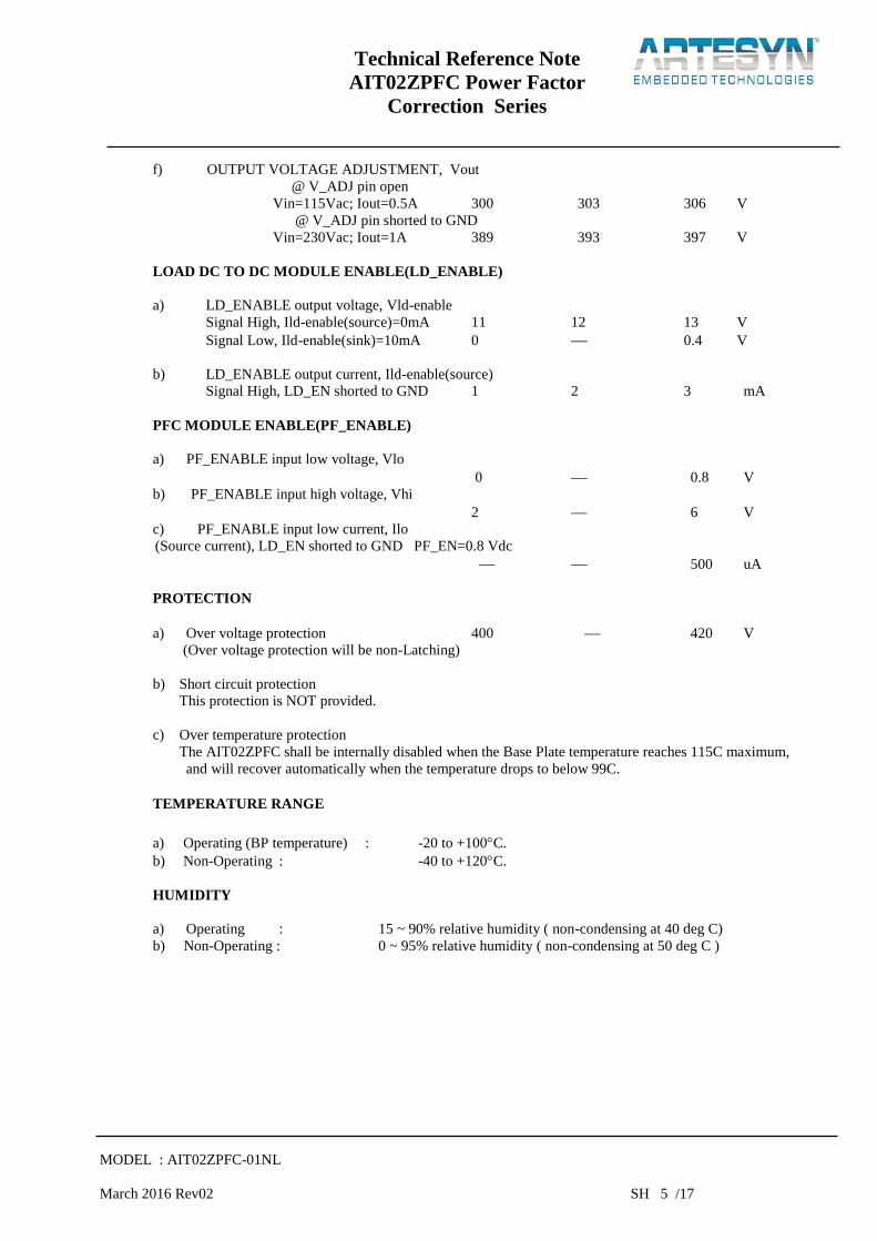
f) OUTPUT VOLTAGE ADJUSTMENT, Vout
@ V_ADJ pin open
Vin=115Vac; Iout=0.5A 300 303 306 V
@ V_ADJ pin shorted to GND
Vin=230Vac; Iout=1A 389 393 397 V
LOAD DC TO DC MODULE ENABLE(LD_ENABLE)
a) LD_ENABLE output voltage, Vld-enable
Signal High, Ild-enable(source)=0mA 11 12 13 V
Signal Low, Ild-enable(sink)=10mA 0 0.4 V
b) LD_ENABLE output current, Ild-enable(source)
Signal High, LD_EN shorted to GND 1 2 3 mA
PFC MODULE ENABLE(PF_ENABLE)
a) PF_ENABLE input low voltage, Vlo
0 0.8 V
b) PF_ENABLE input high voltage, Vhi
2 6 V
c) PF_ENABLE input low current, Ilo
(Source current), LD_EN shorted to GND PF_EN=0.8 Vdc
500 uA
PROTECTION
a) Over voltage protection 400 420 V
(Over voltage protection will be non-Latching)
b) Short circuit protection
This protection is NOT provided.
c) Over temperature protection
The AIT02ZPFC shall be internally disabled when the Base Plate temperature reaches 115C maximum,
and will recover automatically when the temperature drops to below 99C.
TEMPERATURE RANGE
a) Operating (BP temperature) : -20 to +100C.
b) Non-Operating : -40 to +120C.
HUMIDITY
a) Operating : 15 ~ 90% relative humidity ( non-condensing at 40 deg C)
b) Non-Operating : 0 ~ 95% relative humidity ( non-condensing at 50 deg C )
MODEL : AIT02ZPFC-01NL
March 2016 Rev02 SH 6 /17
Technical Reference Note
AIT02ZPFC Power Factor
Correction Series
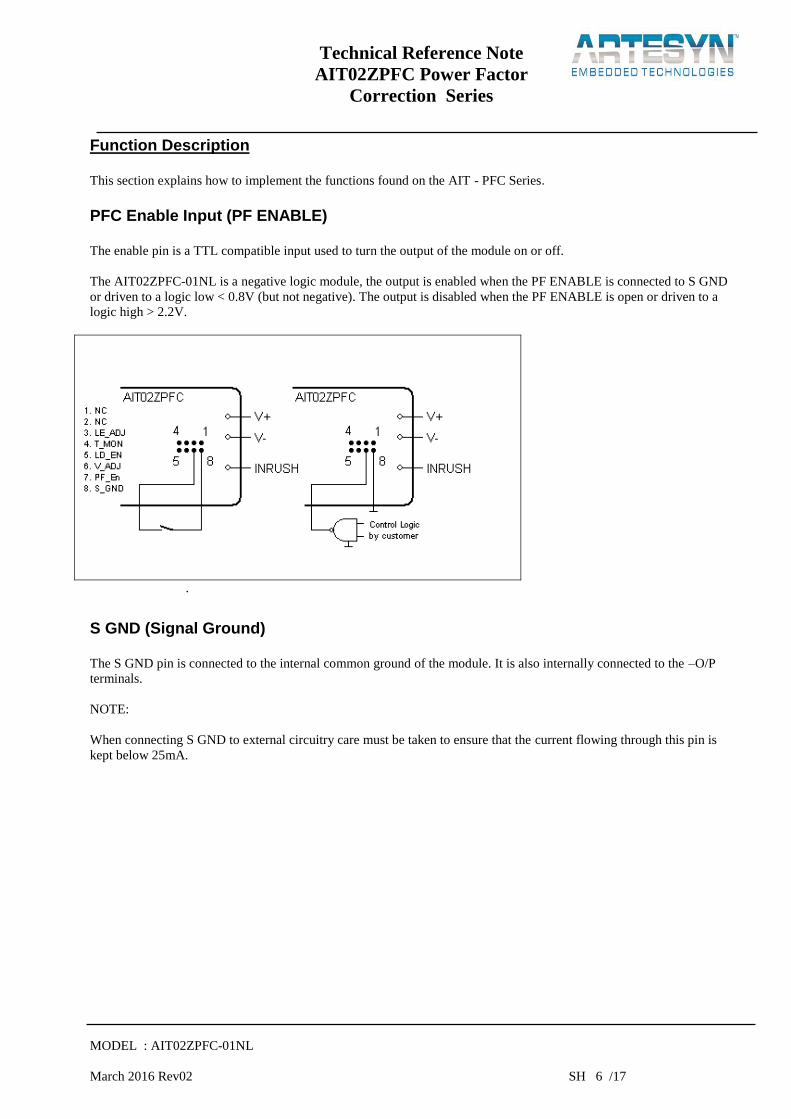
Function Description This section explains how to implement the functions found on the AIT - PFC Series.
PFC Enable Input (PF ENABLE) The enable pin is a TTL compatible input used to turn the output of the module on or off.
The AIT02ZPFC-01NL is a negative logic module, the output is enabled when the PF ENABLE is connected to S GND
or driven to a logic low < 0.8V (but not negative). The output is disabled when the PF ENABLE is open or driven to a
logic high > 2.2V.
.
S GND (Signal Ground) The S GND pin is connected to the internal common ground of the module. It is also internally connected to the –O/P
terminals.
NOTE:
When connecting S GND to external circuitry care must be taken to ensure that the current flowing through this pin is
kept below 25mA.
MODEL : AIT02ZPFC-01NL
March 2016 Rev02 SH 7 /17
Technical Reference Note
AIT02ZPFC Power Factor
Correction Series
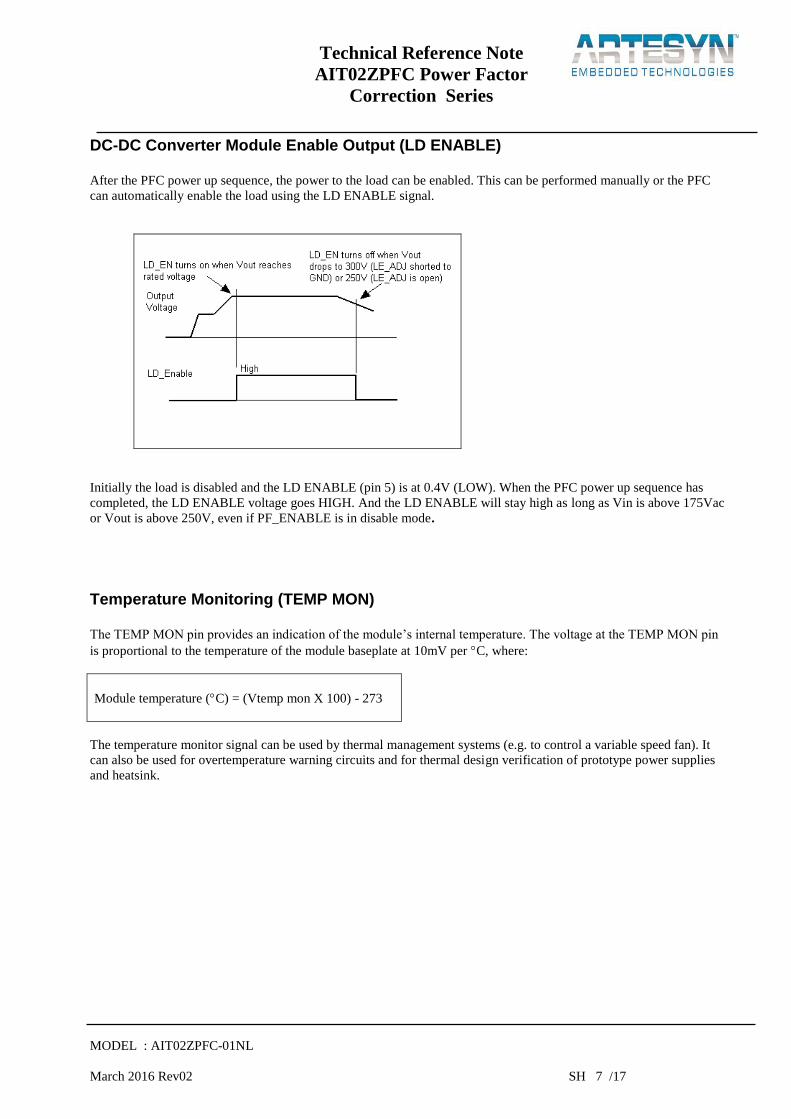
DC-DC Converter Module Enable Output (LD ENABLE) After the PFC power up sequence, the power to the load can be enabled. This can be performed manually or the PFC
can automatically enable the load using the LD ENABLE signal.
Initially the load is disabled and the LD ENABLE (pin 5) is at 0.4V (LOW). When the PFC power up sequence has
completed, the LD ENABLE voltage goes HIGH. And the LD ENABLE will stay high as long as Vin is above 175Vac
or Vout is above 250V, even if PF_ENABLE is in disable mode.
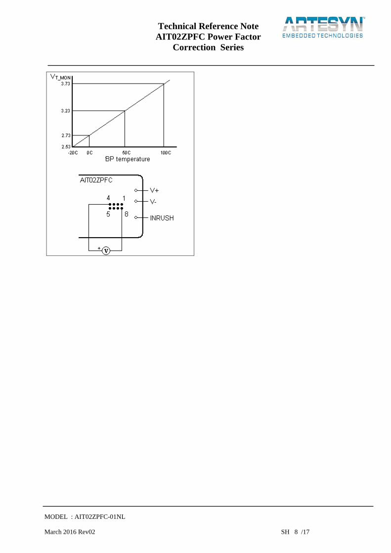
Temperature Monitoring (TEMP MON) The TEMP MON pin provides an indication of the module’s internal temperature. The voltage at the TEMP MON pin
is proportional to the temperature of the module baseplate at 10mV per C, where:
Module temperature (C) = (Vtemp mon X 100) - 273
The temperature monitor signal can be used by thermal management systems (e.g. to control a variable speed fan). It
can also be used for overtemperature warning circuits and for thermal design verification of prototype power supplies
and heatsink.
MODEL : AIT02ZPFC-01NL
March 2016 Rev02 SH 8 /17
Technical Reference Note
AIT02ZPFC Power Factor
Correction Series
MODEL : AIT02ZPFC-01NL
March 2016 Rev02 SH 9 /17
Technical Reference Note
AIT02ZPFC Power Factor
Correction Series
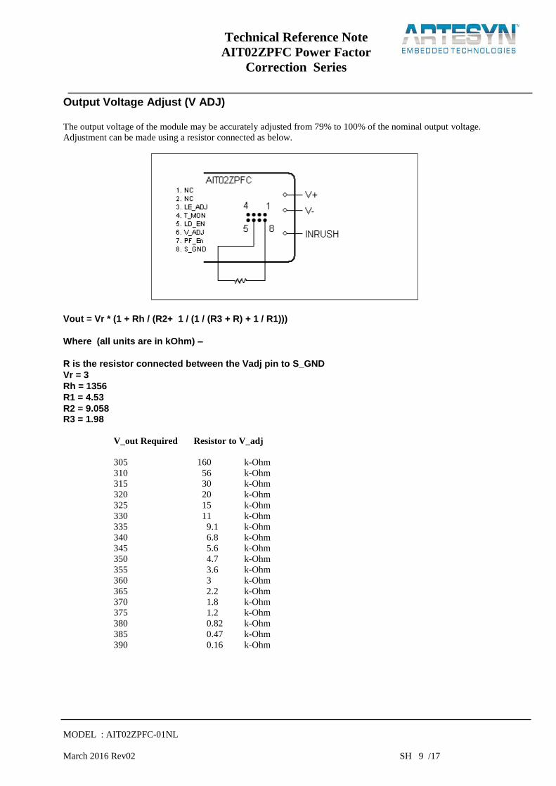
Output Voltage Adjust (V ADJ) The output voltage of the module may be accurately adjusted from 79% to 100% of the nominal output voltage.
Adjustment can be made using a resistor connected as below.
Vout = Vr * (1 + Rh / (R2+ 1 / (1 / (R3 + R) + 1 / R1)))
Where (all units are in kOhm) –
R is the resistor connected between the Vadj pin to S_GND
Vr = 3
Rh = 1356
R1 = 4.53
R2 = 9.058 R3 = 1.98
V_out Required Resistor to V_adj
305 160 k-Ohm
310 56 k-Ohm
315 30 k-Ohm
320 20 k-Ohm
325 15 k-Ohm
330 11 k-Ohm
335 9.1 k-Ohm
340 6.8 k-Ohm
345 5.6 k-Ohm
350 4.7 k-Ohm
355 3.6 k-Ohm
360 3 k-Ohm
365 2.2 k-Ohm
370 1.8 k-Ohm
375 1.2 k-Ohm
380 0.82 k-Ohm
385 0.47 k-Ohm
390 0.16 k-Ohm
MODEL : AIT02ZPFC-01NL
March 2016 Rev02 SH 10 /17
Technical Reference Note
AIT02ZPFC Power Factor
Correction Series
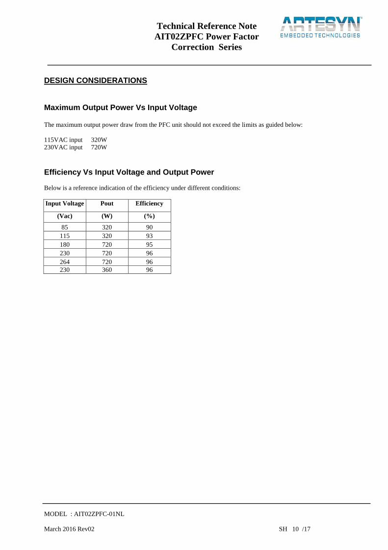
DESIGN CONSIDERATIONS Maximum Output Power Vs Input Voltage The maximum output power draw from the PFC unit should not exceed the limits as guided below:
115VAC input 320W
230VAC input 720W
Efficiency Vs Input Voltage and Output Power
Below is a reference indication of the efficiency under different conditions:
Input Voltage Pout Efficiency
(Vac) (W) (%)
85 320 90
115 320 93
180 720 95
230 720 96
264 720 96
230 360 96
MODEL : AIT02ZPFC-01NL
March 2016 Rev02 SH 11 /17
Technical Reference Note
AIT02ZPFC Power Factor
Correction Series
Input Undervoltage Protection An input undervoltage protection circuit protects the module under low input voltage conditions. Hysteresis is built into
the PFC Series module to allow for high levels of variation on the input supply voltage without causing the module to
cycle on and off. PFC modules will operate when the input exceeds 82Vac and turn off below 77Vac (norminal).
Input Fusing ASTEC modules do not have an in-line fuse fitted internally. In order to comply with CSA, VDE and UL safety
regulations it is recommended that a fuse of 250Vac, 10A be fitted at the module’s input.
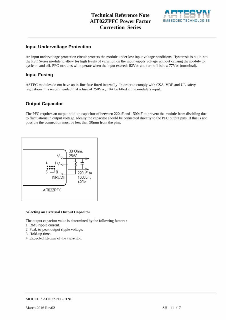
Output Capacitor The PFC requires an output hold-up capacitor of between 220uF and 1500uF to prevent the module from disabling due
to fluctuations in output voltage. Ideally the capacitor should be connected directly to the PFC output pins. If this is not
possible the connection must be less than 50mm from the pins.
Selecting an External Output Capacitor
The output capacitor value is determined by the following factors :
1. RMS ripple current.
2. Peak-to-peak output ripple voltage.
3. Hold-up time.
4. Expected lifetime of the capacitor.
MODEL : AIT02ZPFC-01NL
March 2016 Rev02 SH 12 /17
Technical Reference Note
AIT02ZPFC Power Factor
Correction Series
RMS ripple current The maximum permissible rms ripple current for the output capacitor should be greater than the rms ripple current for
the application. The ripple current for the PFC module can be approximated as
Irms
= (PO/Eff) x 1/(V
O x V
rms)
where :
PO
= output power (W)
Eff = efficiency
VO = output voltage (V)
Vrms
= input rms voltage (V)
This gives the ripple current at 125KHz. The maximum ripple current for capacitors is usually specified at 120Hz. To
convert from 125KHz to 120Hz the Irms figure should be divided by 1.3 .
Peak to Peak Output Ripple Voltage The ac input causes a ripple on the output voltage. The size of the ripple is inversely proportional to the size of the
capacitor. Therefore the maximum allowable ripple voltage should be decided in order to calculate the size of capacitor
required. This may be calculated using the following equation:
CO = P
O / (2f x Eff x V
O x V
ripple)
where :
CO = output capacitance (µF)
Eff = efficiency
f = input voltage frequency (Hz)
VO = output voltage (V)
Vripple
= output ripple voltage (V)
Hold-Up Time Requirement
The output capacitor value is different for different hold-up time requirements. The minimum capacitance
corresponding to the required hold-up time of a system comprised of ASTEC DC/DC power modules and an PFC
module can be calculated as follows:
CO min
= (2 x PO
x Thold
)/[(VO-V
ripple)2 - (V
min)2]
where :
CO min
= output capacitance (µF)
PO
= output power (W)
Thold
= hold up time (sec)
VO = output voltage (V)
Vripple
= output ripple voltage (V)
Vmin
= minimum input voltage for DC/DC module
MODEL : AIT02ZPFC-01NL
March 2016 Rev02 SH 13 /17
Technical Reference Note
AIT02ZPFC Power Factor
Correction Series
For example:
A PFC module driving 3 AIF80A300 400W modules @ 5V. Efficiency of the AIF80A300 module is 88%, the
minimum input voltage is 250V, the output voltage of the PFC is 380V, the required hold-up time is 20mS and the
peak-to-peak voltage Vripple
is chosen to be 16V.
CO min
= 2 x (3 x 400/0.88) x 0.02 = 390µF (470 µF 20%)
[(380-16)2-2502]
This figure is the minimum capacitance. To allow for capacitor tolerances and aging effects the actual value should
generally be around 1.5 times greater.
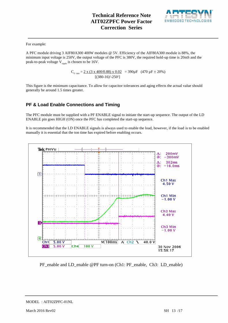
PF & Load Enable Connections and Timing The PFC module must be supplied with a PF ENABLE signal to initiate the start-up sequence. The output of the LD
ENABLE pin goes HIGH (ON) once the PFC has completed the start-up sequence.
It is recommended that the LD ENABLE signals is always used to enable the load, however, if the load is to be enabled
manually it is essential that the ton time has expired before enabling occurs.
PF_enable and LD_enable @PF turn-on (Ch1: PF_enable, Ch3: LD_enable)
MODEL : AIT02ZPFC-01NL
March 2016 Rev02 SH 14 /17
Technical Reference Note
AIT02ZPFC Power Factor
Correction Series
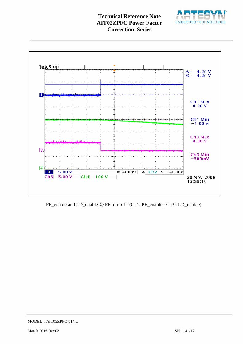
PF_enable and LD_enable @ PF turn-off (Ch1: PF_enable, Ch3: LD_enable)
MODEL : AIT02ZPFC-01NL
March 2016 Rev02 SH 15 /17
Technical Reference Note
AIT02ZPFC Power Factor
Correction Series
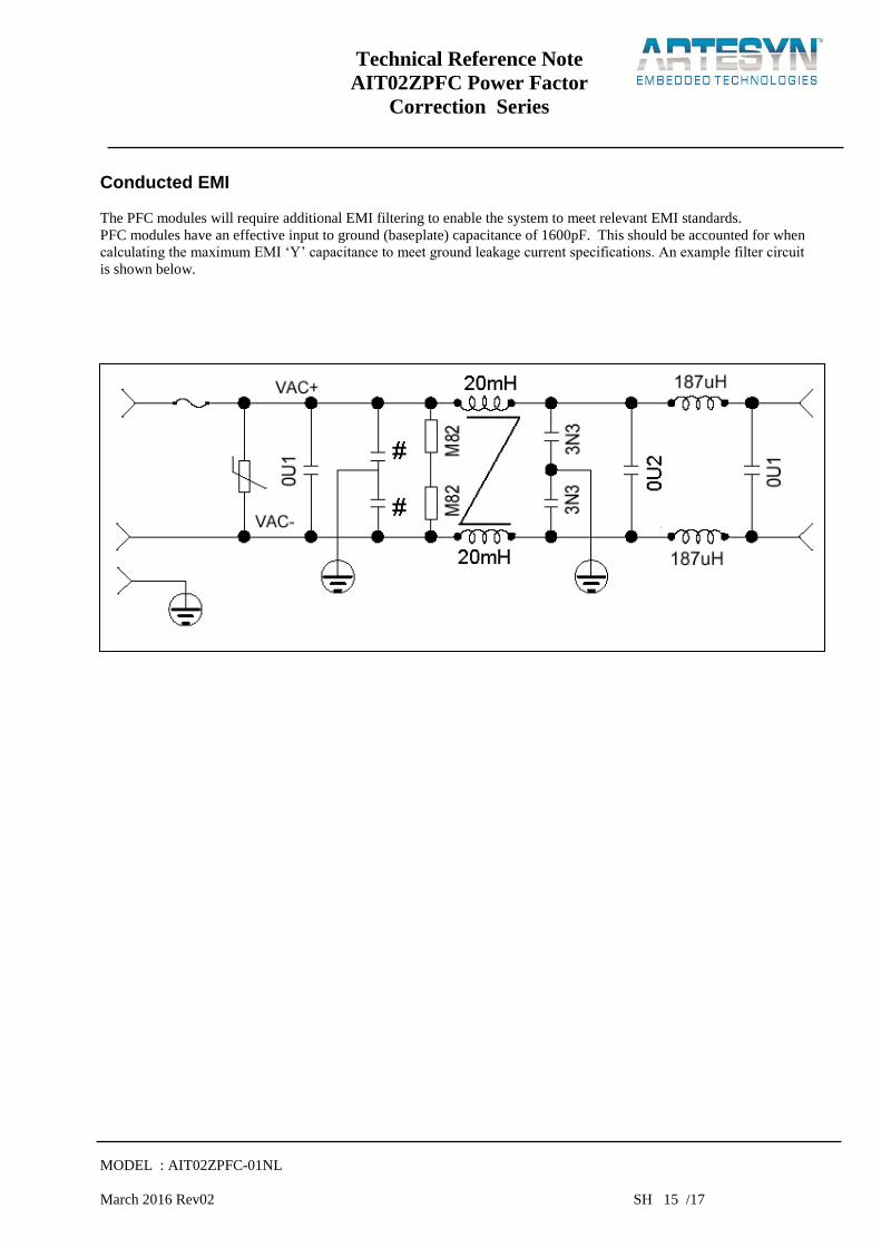
Conducted EMI The PFC modules will require additional EMI filtering to enable the system to meet relevant EMI standards.
PFC modules have an effective input to ground (baseplate) capacitance of 1600pF. This should be accounted for when
calculating the maximum EMI ‘Y’ capacitance to meet ground leakage current specifications. An example filter circuit
is shown below.
MODEL : AIT02ZPFC-01NL
March 2016 Rev02 SH 16 /17
Technical Reference Note
AIT02ZPFC Power Factor
Correction Series
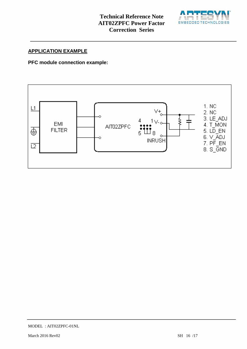
APPLICATION EXAMPLE
PFC module connection example:
MODEL : AIT02ZPFC-01NL
March 2016 Rev02 SH 17 /17
Technical Reference Note
AIT02ZPFC Power Factor
Correction Series
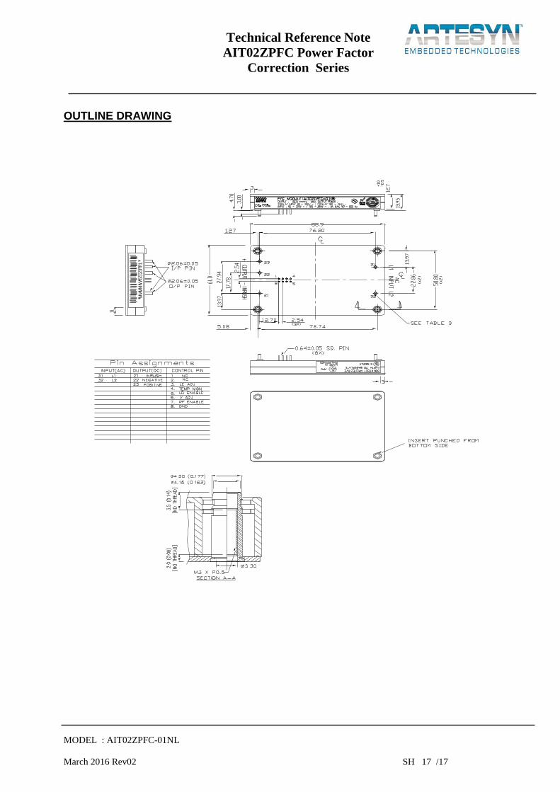
OUTLINE DRAWING