Embed Size (px)
Citation preview
ELECTROSTATIC DISCHARGE PROPERTIES OF IRRADIATED NANOCOMPOSITES
THESIS
Joshua D. McGary, Major, USA
AFIT/GNE/ENP/09-M03
DEPARTMENT OF THE AIR FORCE
AIR UNIVERSITY
AIR FORCE INSTITUTE OF TECHNOLOGY
Wright-Patterson Air Force Base, Ohio
APPROVED FOR PUBLIC RELEASE; DISTRIBUTION UNLIMITED

The views expressed in this thesis are those of the author and do not reflect the official policy or position of the United States Air Force, Department of Defense, or the United States Government.
AFIT/ENP/GNE/09-M03
ELECTROSTATIC DISCHARGE PROPERTIES
OF IRRADIATED NANOCOMPOSITES
THESIS
Presented to the Faculty
Department of Engineering Physics
Graduate School of Engineering and Management
Air Force Institute of Technology
Air University
Air Education and Training Command
In Partial Fulfillment of the Requirements for the
Degree of Master of Science in Nuclear Engineering
Joshua D. McGary, BS
Major, USA
March 2009
APPROVED FOR PUBLIC RELEASE; DISTRIBUTION UNLIMITED

iv
AFIT/GNE/ENP/09-M03
Abstract
Modernization in space systems requires employment of new light-weight, high
performance composite materials that reduce bulk weight and increase structural
integrity. This thesis explored the behavior of one such material prior to and following a
35-year simulated space radiation life-cycle. Select electrical properties of nickel
nanostrandTM-carbon composites in seven configurations were characterized prior to
electron irradiation via surface and bulk resistivity measurements and contact
electrostatic discharge (ESD) measurements. Following irradiation at a fluence of 1016 e-
/cm2 at an average energy of 500 keV, measurements were repeated and compared
against pre-irradiation data. Configuration D is the best suited for use as a satellite
external surface material. All composite configurations tested in this research showed
degradation in critical electrical properties when examined in the aggregate. The data
showed no common trend between composites’ electrical performance based on location
or density of the nickel nanostrands™ in the material. Following radiation exposure,
surface resistivity increased for all configurations while bulk resistivity change correlated
to the type of epoxy resin used in the composite. The mechanism responsible for these
changes is electron induced displacement damage within both the epoxy and carbon
which reduce permittivity and, or conductivity within the bulk. ESD current waveform
properties of peak current and decay time decreased in a manner sufficient to conclude
that every configuration tested is subject to increased ESD frequency and intensity over a
lifetime of space radiation. These materials require further engineering to better resist the
changes noted in these electrical properties before used as satellite surfaces.

v
Acknowledgements
I would like to thank Dr. James Petrosky for his insight and wisdom throughout
this work and through my tenure at AFIT. Dr. Gary C. Farlow, WSU, was instrumental
in helping me understanding the physics behind the radiation experiments and in gaining
an appreciation for the complexities of electron accelerators. The Air Force Research
Laboratory – Materials and Manufacturing Directorate, as well as the Electrostatic
Discharge Laboratory provided excellent lab support and assistance with refining the
experimental procedures. The fabrication shop; Jan, Jason and Dan were flexible, fast
and professional, and this work could not have been completed without their expertise.
Joshua D. McGary

vi
Table of Contents
Page
Abstract .............................................................................................................................. iv
Acknowledgements ...............................................................................................................v
Table of Contents ............................................................................................................... vi
List of Figures .................................................................................................................. viii
List of Tables ...................................................................................................................... xi
List of Symbols and Acronyms .......................................................................................... xii
I. Introduction ......................................................................................................................1
1.2 Objective ............................................................................................................................... 7 1.3 Paper Organization .............................................................................................................. 7
II. Theory .............................................................................................................................9
2.1 Characterizing the Problem ................................................................................................ 9 2.1.1 The Space Environment .............................................................................................. 9 2.1.2 Satellite Charging and Discharging ......................................................................... 13 2.1.3 Simulating Space Radiation Induced Damage Mechanisms in Dielectrics ........ 16 2.1.4 Nanocomposites and Associated Electrical Properties ......................................... 19 2.1.5 Radiation effects on nanostrand based composites ............................................... 23
2.2 Current Standards for Space Systems ESD Testing and Vehicle Validation ............ 25 2.3 The ESD Discharge Pulse and Parameters of Interest ................................................. 30 2.4 Summary ............................................................................................................................ 33
III. Methods of Experimentation........................................................................................35
3.1 Introduction ........................................................................................................................ 35 3.2 Materials Under Test ........................................................................................................ 35 3.3 Test Specimen Preparation ............................................................................................... 41 3.5 Bulk Resistivity Measurements ....................................................................................... 49 3.6 Electrostatic Discharge Test and Procedures ................................................................. 52
3.6.1 Electrostatic Discharge Current Equations ............................................................. 60 3.6.2 Current Pulse Analysis via Genetic Algorithms .................................................... 61
3.7 Electron Irradiation Procedures ....................................................................................... 64 3.7.1 Electron Energy Selection......................................................................................... 66 3.7.2 Dosimetry Calculations ............................................................................................. 69
3.8 Summary ............................................................................................................................ 70
IV. Results and Discussion ................................................................................................71
4.1 Bulk Resistance Results ................................................................................................... 71 4.2 Surface Resistivity Results............................................................................................... 75 4.3 ESD Results ....................................................................................................................... 79

vii
Page 4.3.1 Genetic Algorithm Solutions to ESD Equations in Early Time .......................... 81 4.3.2 Genetic Algorithm Solutions to ESD Equations in Late Time ............................ 86
4.4 Measurement Summary .................................................................................................... 87
V. Conclusions ..................................................................................................................91
5.1 Summary ............................................................................................................................. 91 5.2 Conclusions ........................................................................................................................ 91 5.3 Recommendations for Future Research ......................................................................... 94
Appendix A: Genetic Algorithm ........................................................................................96
Bibliography ....................................................................................................................102

viii
List of Figures
Figure Page
1. 100 nm Diameter Nickel Nanostrands™ at 50,000 x Magnification ...............................4
2. 625kV ESD test performed on Fabric with Nanostrand™ infusion (left) ........................5
3. Schematic of the Earth’s Magnetosphere and Plasma Densities ...................................11
4. Physical Processes Resulting in Surface Charging in Space .........................................15
5. Primary Electron-Material Interaction Mechanisms ......................................................18
6. Volume Resistivity Resulting from Methods of NanostrandTM production ..................21
7. Volume Resistivity of Nanostrands ™ Under Compression and Tension ......................21
8. Conductivity Comparison for Nanostrands™ in Resin ...................................................22
9. Specific Conductivity Comparison for Nickel Nanostrands™ .......................................23
10. NASA Image of the MISSE Panel. ..............................................................................25
11. Configuration A Image at x5 Magnification. ...............................................................36
12. Configuration B Image at x5 Magnification ................................................................37
13. Configuration C Image at x5 Magnification ................................................................37
14. Configuration M Image at x5 Magnification ...............................................................38
15. Configuration I Image at x5 Magnification. ................................................................39
16. Configuration Ext Image at x5 Magnification .............................................................39
17. Configuration D Image at x5 Magnification. ...............................................................40
18. Configuration E Image at x5 Magnification. ...............................................................41
19. One-inch Diameter Disk Samples ................................................................................42
20. Surface Resistivity Test Set-up ....................................................................................44
ix
Figure Page
21. Close-up View of Four-point Surface Resistivity Test Fixture ...................................44
22. Cross-sectional View of Surface Resistivity Measurement. ........................................45
23: Example Surface Resistance Curves for Configuration I ............................................47
24. Example Plot of Mean Current vs. Voltage Difference Curves ..................................48
25. Complete Bulk Resistivity Test Aparatus ....................................................................50
26. Detailed View of Bulk Resistivity Test Fixture ...........................................................50
27. Pre-Irradiation Mean Bulk Resistivity Example Plot. .................................................52
28. ESD Test Set-up with Critical Equipment and Components .......................................54
29. Equivalent Circuit Model Used for ESD Testing. .......................................................54
30. Current Waveform of a Typical ESD Baseline Pulse ..................................................55
31. Minizap® ESD Simulator Waveforms for Comparison Against EIC 801-2 ................57
32. Mean ESD Waveform Plot for Configuration B..........................................................59
33. Genetic Algorithm Flow Chart ....................................................................................62
34. Example Comparison of the Experimental Data and GA Fit for 12 kV ESD .............64
35. Van de Graaf Electron Accelerator Image. ..................................................................65
36. AFIT "Cold Head" Sample Mounting Image. .............................................................66
37. CASINO® Electron Deposition Simulation. ...............................................................67
38. 500 keV CASINO® Electron Range Simulation ..........................................................68
39. 1000 keV CASINO® Electron Range Simulation .......................................................68
40. Pre and Post-Irradiation Bulk Resistivity Comparison. ...............................................72
41. Pre and Post-Irradiation IV Comparison for Configuration Ext. .................................76
42. Pre and Post-Irradiation IV Comparison for Configuration C. ....................................77

x
Figure Page
43. Pre and Post-Irradiation Surface Resistivity Comparison. ..........................................78
44. Pre and Post-Irradiation Current Waveforms for Configuration D. ............................80
45. Pre and Post-Irradiation Current Waveforms for Configuration I ...............................81
46. GA Fit to Experimental data for 0-6 ns ESD Current Waveform. ...............................82

xi
List of Tables
Table Page
1. Minimum Plasma Particle Tolerance Thresholds for USAF Space Vehicles................13
2. ESD Source Generation Options and Comparison. .......................................................29
3.Sample Configuration Matrix. ........................................................................................35
4. Pre-Radiation Mean Surface Resistivity. .......................................................................48
5. IEC 801-2 Baseline ESD Waveform Specifications. .....................................................56
6. Output Current Waveform for Minizap® ESD Generator .............................................57
7. Mean Bulk Resistivity Pre and Post-Irradiation. ...........................................................73
8. Mean Surface Resistivity Pre and Post-Irradiation .......................................................78
9. ESD Current and Timing Parameters for 12kV Discharge. ...........................................84

xii
List of Symbols and Acronyms
Å Angstrom [10-10 meters]
A Sample Configuration with 0 gsm Ni, of Composite Group Number One
A Ampere measure of current
AFRL/RX Air Force Research Laboratory – Materials and Manufacturing Directorate
ASTM American Society of Testing and Materials
B External Configuration with 174 gsm Ni, of Composite Group One
C Interwoven Configuration with 242 gsm Ni, of Composite Group One
CNC Computer Numerical Control
CASINO® Monte Carlo Simulation of Electron Trajectories in Solids
CSDA Continuous Slowing Down Approximation
CDT Contact Discharge Test
CVR Current Viewing Resistor
D Sample Configuration with 260 gsm Ni, of Composite Group Three
DMM Digital Multimeter
DoD Department of Defense
E Sample Configuration with 0 gsm Ni, of Composite Group Three
ε Permittivity [F/m]
e- Electron
Ed Displacement Energy
eV Electron Volt
EMI Electromagnetic Interference

xiii
ESD Electrostatic Discharge
Ext External Configuration with 200 gsm Ni, of Composite Group Two
GA Genetic Algorithm
GEO Geosynchronous Earth Orbit
gsm Grams per square meter [references Ni content]
HDPE High Density Polyethylene
hPa Hectopascal [1 hPa=100 Pa]
I Interlaminar Configuration with 200 gsm Ni, of Composite Group Two
I Current [A]
IEC International Electro-technical Commission
Ip Peak Current
IV Current verses Voltage
keV Kilo Electron Volt [103 eV]
km Kilometer
kV Kilovolt
LEO Low Earth Orbit
LTAPCVD Low Temperature Atmospheric Pressure Chemical Vapor Decomposition
M Midplane Configuration with 200gsm Ni, of Composite Group Two
mA Milliamp [10-3 A]
MeV Mega Electron Volt [106 eV]
MIL-STD Military Standard
MISSE Material International Space Station Experiment
nA Nanoamp [10-9 A]

xiv
NASA National Aeronautics and Space Administration
Ni Nickel
NIEL Non-ionizing Energy Loss
NIST National Institute of Standards and Technology
NNS Nickel Nanostrands™
ONERA French National Aerospace Laboratory
S Siemens
tf Pulse Fall or Decay Time [ns]
tp Pulse Width [ns]
tr Pulse Rise Time [ns]
torr Measure of Pressure (vacuum) torr = 133.3 Pa
Vbr Breakdown voltage
VDG Van de Graaf Electron Accelerator
ρ Resistivity [Ω-cm]
Ω Resistance [Ω]
µm Micrometers [10-6 m]

1
ELECTROSTATIC DISCHARGE PROPERTIES
OF IRRADIATED NANOCOMPOSITES
I. Introduction
Since the dawn of man’s foray into space with the launch of Sputnik I on October
4, 1957, the struggle to build strong, reliable and economical space systems has become
paramount to continued expansion of both military and civilian enterprise in the harsh
environment of geosynchronous orbit. As technological advancements in many
disciplines increase our long-range communication, surveillance, and exploration
capabilities, the space systems which support these technologies must increase similarly
in endurance, structural rigidity, and cost minimization. These requirements provide the
impetus for continued modernization of space platforms with new materials that can
safeguard critical components in the extreme conditions of space.
The space environment consists of highly energetic, low density charged particles
that flow in both the earth’s magnetosphere and the solar wind. These particles interact
with satellite surfaces primarily through stripping interactions, as well as through the
Compton and photoelectric effect that deposit charge over the incident surfaces.
Energetic particles not only charge the surface of the space vehicle, they also penetrate to
variable depths within the material. At certain energies, these particles can cause both
ionization and displacement damage within the material. These interactions, while
harmless on large conductive surfaces, can cause adverse affects in composite dielectric
materials. As the dielectric’s electro-mechanical properties degrade through prolonged

2
exposure, the potential for electrostatic discharge (ESD) increases at frequencies and
intensities beyond the spacecraft’s design tolerance.
Over time, dielectric materials build up large charge differentials. If there is no
mechanism for relaxing the material back to charge equilibrium, the potential difference
eventually overcomes the material’s ability to contain the charge and the material breaks
down, releasing charge through an ESD. ESD is a parasitic phenomena experienced by
all materials in space to varying degrees of destructiveness, from routine charge
relaxation to high current arcing resulting in component burn-out or total vehicle failure
[3].
Destructive ESD was first noted in the 1960s via spurious high-voltage charging
on the ATS-5 satellite [3]. The problem grew more serious, as research and innovation in
the following decades resulted in a drastic increase in circuit complexity as well as
component size reduction. Size reduction resulted in an increased propensity for device
coupling to the ESD waveform. This tendency was proven on June 2, 1973, with the
total loss of the DSCS-9431 satellite [3,5]. Subsequently, with more than 160
documented occurrences of major ESD anomalies and five additional complete mission
failures through 1997, ESD proves to be the largest damage mechanism and risk to space
systems [6,10].
The electrical properties of satellite materials determine the frequency of, and a
vehicle’s susceptibility to surface generated ESD. Chosen for its high conductivity and
strength as well as its relatively low cost, the historical structural and shielding material
of choice was aluminum. However, composite materials have emerged in the last ten
years as a better choice for satellite external surfaces. Composites possess more ideal

3
thermal properties, higher strength, and better resistance to vibrational loading than
aluminum. These factors, combined with low manufacturing cost and extreme light
weight, have established composites as a material of choice for spacecraft designers since
the early 1990s [2].
The tradeoff to composites’ exceptional material properties is their inherently less
desirable electrical properties, especially compared to those present in aluminum.
Composites are highly dielectric. When used as external surface material in satellite
design, these materials significantly increase the vehicle’s susceptibility to ESD, both in
frequency and intensity. The study of ESD mitigation and control in composite based
external surfaces is thus becoming increasingly critical to designing long-life spacecraft
capable of adequately safeguarding critical internal components.
A recent partnership between Metal Matrix Composites LLC (Metal Matrix) of
Heber, Utah, and the Air Force Research Laboratory’s Materials and Manufacturing
Directorate at Wright-Patterson Air Force Base (AFRL/RX) has yielded a process that
utilizes various methods to infuse conductive materials into the matrix of carbon
composites. Of primary interest is the addition of highly conductive nickel chains,
termed nickel nanostrandsTM. These nickel filaments range in diameter from 50 to 1000
nm and vary in length from microns to millimeters (Figure 1). Nickel nanostrandsTM are
integrated into the composite material in several ways, the most common of which is by
compressing the nickel mesh to a density and porosity dictated by the customer then
infusing it into the nanostrand preform. These layers are then machined to the desired
dimensions and layered into the composite ply in the requisite configuration. This
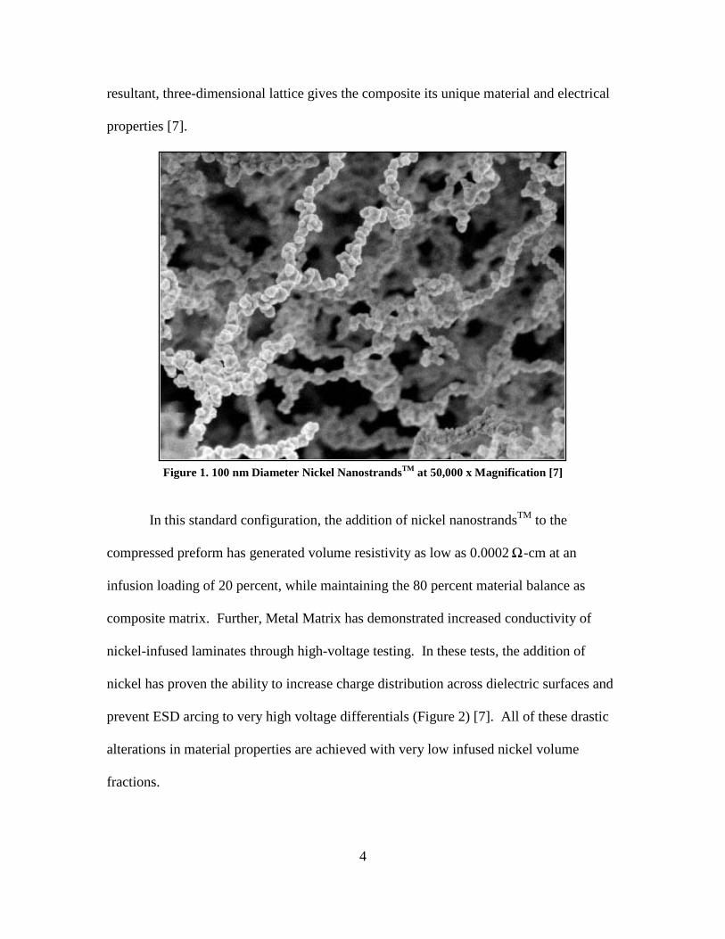
4
resultant, three-dimensional lattice gives the composite its unique material and electrical
properties [7].
Figure 1. 100 nm Diameter Nickel NanostrandsTM at 50,000 x Magnification [7]
In this standard configuration, the addition of nickel nanostrandsTM to the
compressed preform has generated volume resistivity as low as 0.0002 Ω-cm at an
infusion loading of 20 percent, while maintaining the 80 percent material balance as
composite matrix. Further, Metal Matrix has demonstrated increased conductivity of
nickel-infused laminates through high-voltage testing. In these tests, the addition of
nickel has proven the ability to increase charge distribution across dielectric surfaces and
prevent ESD arcing to very high voltage differentials (Figure 2) [7]. All of these drastic
alterations in material properties are achieved with very low infused nickel volume
fractions.
5
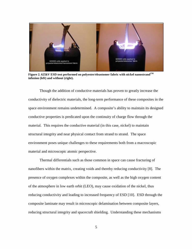
Figure 2. 625kV ESD test performed on polyester/eleastomer fabric with nickel nanostrandTM infusion (left) and without (right).
Though the addition of conductive materials has proven to greatly increase the
conductivity of dielectric materials, the long-term performance of these composites in the
space environment remains undetermined. A composite’s ability to maintain its designed
conductive properties is predicated upon the continuity of charge flow through the
material. This requires the conductive material (in this case, nickel) to maintain
structural integrity and near physical contact from strand to strand. The space
environment poses unique challenges to these requirements both from a macroscopic
material and microscopic atomic perspective.
Thermal differentials such as those common in space can cause fracturing of
nanofibers within the matrix, creating voids and thereby reducing conductivity [8]. The
presence of oxygen complexes within the composite, as well as the high oxygen content
of the atmosphere in low earth orbit (LEO), may cause oxidation of the nickel, thus
reducing conductivity and leading to increased frequency of ESD [10]. ESD through the
composite laminate may result in microscopic delamination between composite layers,
reducing structural integrity and spacecraft shielding. Understanding these mechanisms

6
and the interaction between space radiation and nickel-carbon composites is the focus of
this research. Thorough understanding of these interaction mechanisms will aid in
spacecraft design and construction that compensates for or completely overcomes the
degradation resulting from ESD.
Many of the material properties of nickel nanostrand™ composite materials were
recently examined at AFIT. It was determined that neither ultimate tensile strength,
Young’s modulus, nor structural failure change as a function of nickel content, the
nickel-carbon ply configuration, or exposure to a simulated space environment. The
research further concluded that including nickel nanostrandTM layers within the carbon
composite result in a 25 percent increase in electromagnetic interference (EMI) shielding
[2]. Thus, from a material science perspective, the simulated space environment does not
significantly degrade the structural integrity of nickel-carbon nanocomposites.

7
1.2 Objective
This thesis focuses on the damaging effects of the simulated space environment
(electron radiation) on nickel nanostrandTM-infused composites. Further, it examines the
ancillary effects of radiation-induced damage on the long-term ESD properties of the
material and the frequency with which ESD might occur as a byproduct of irradiation.
The objectives of this work are as follows:
1. Design and build ESD, surface resistivity, and bulk resistance test platforms and experiments that meet US Military (MIL-STD) and NASA standards and directives, and that are compatible for proof of concept in future ESD testing of this type.
2. Validate the simulated space environment as a suitable comparison to the actual exposure energies and fluences that cause damage to nickel-carbon nanocomposites.
3. Measure select electrical properties of nickel-carbon nanocomposites prior to and following electron irradiation.
a. Measure Surface Resistivity b. Measure Bulk Resistivity c. Measure Current Waveform following ESD
4. Determine how nickel-carbon nanocomposites compare to the MIL-STD for
ESD protection following electron irradiation.
5. Analyze the capacity of these materials to serve as reliable shielding and structural components through long-term use in the space environment.
1.3 Paper Organization
This thesis will address theory (characterization of the problem); experimental
design, results and discussion; and provide conclusions. The theory section offers a
primer on the space environment and its associated radiation, details of the composite
materials used in the experiment and associated physical properties, as well as the
national standards for ESD testing and comparison. The experimental section details the

8
design of experiments used and includes the pre-irradiation characterization
measurements and data. The results and discussion section details the post-irradiation
results and associated analysis. Finally the conclusions section offers analysis of the
results and recommendations for follow-on research with nickel-carbon nanocomposites.

9
II. Theory
2.1 Characterizing the Problem
Proper replication and analysis of three equally important competing factors allow
one to quantify a space vehicle’s susceptibility to electrostatic discharge. These three
factors are: ESD source, material and experiment. The ESD source emanates from large
surface charge differentials that result from exposure to the radioactive space
environment. Simulating the correct energy and fluence of this radiation is critical to
analyzing the damage mechanisms within the composite. The propensity for a material
to electrically discharge is determined by several properties, most telling of which are
surface and bulk resistivity. Proper design of experimental test fixtures and methods of
data collection with regard to repeatability and error minimization dictate the quality of
the analysis and allow one to determine the effects of material-radiation interactions.
Finally, the quality and reliability of the experimental design replicating the ESD is
paramount to qualifying a material’s potential for use in the space environment. This is
accomplished through adherence to published ESD directives and standards of both the
military and international ESD community. The synergy of these three factors is the
basis for this research and will be discussed in detail herein.
2.1.1 The Space Environment
The majority of satellites operate in geostationary and low earth orbits
(GEO/LEO), from 200 to 35,000 kilometers above the earth’s surface. Military satellites,
primarily due to their unique reconnaissance mission, often have greatly variable orbits
designed to provide wide area or precision coverage, and as a result are exposed to a
broad range of radiation energies and fluxes. The degree to which a satellite is exposed

10
to radiation is dependent upon its location with respect to the sun, the Earth’s
magnetosphere, and the level of solar activity; as well as the cross-sectional area of the
satellite exposed to the radiation stream [1].
The space environment is characterized as low-density plasma populated with
charged particles. The plasma density and composition vary greatly with altitude above
the earth. Near the surface of the earth (300 km), the average operating altitude for LEO
satellites, the plasma density averages 106 particles/cm3. Outside the magnetosphere
(70,000 km) the plasma density drops to approximately 5 particles/cm3 [13]. As altitude
increases, plasma density decreases faster at higher latitudes and generally follows the
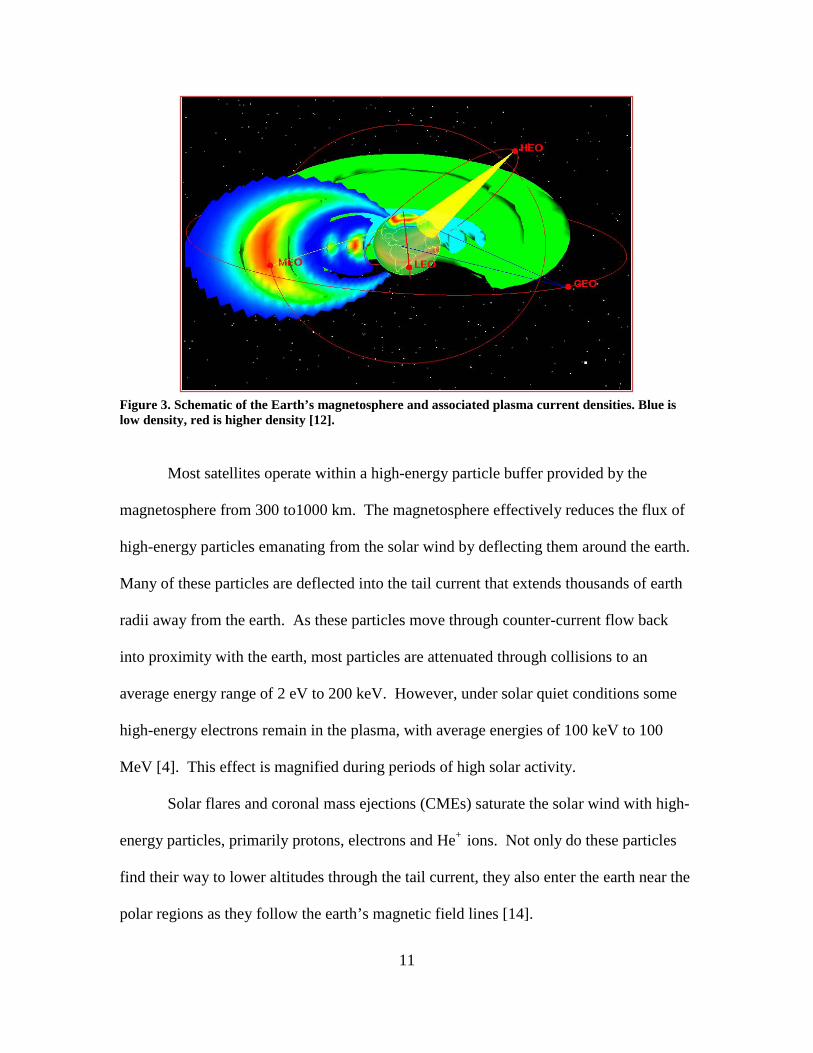
configuration of the earth’s magnetic field lines [14]. This phenomenon is shown in
Figure 3.
Plasma constituents change with density and altitude and thus the damage
mechanisms associated with each form of radiation must be accounted for in satellite
surface design. The effective boundary layer where plasma density drops by a factor of
approximately 50 is called the plasmapause. Between the upper atmosphere and the
plasmapause are varying concentrations of constituents. Ionized atomic Oxygen (O+),
Oxygen (O2+) and NO+ are the primary constituents at the lower limits of LEO, while O+
and hydrogen ions (H+) dominate from 300 to 1000 km above ground level; above 1200
km, H+ and Helium ions (He+) are most prevalent [14]. Military satellites must be
designed to retain their structural and electrical integrity throughout a lifetime of
exposure to these damaging plasma constituents.
11
Figure 3. Schematic of the Earth’s magnetosphere and associated plasma current densities. Blue is low density, red is higher density [12].
Most satellites operate within a high-energy particle buffer provided by the
magnetosphere from 300 to1000 km. The magnetosphere effectively reduces the flux of
high-energy particles emanating from the solar wind by deflecting them around the earth.
Many of these particles are deflected into the tail current that extends thousands of earth
radii away from the earth. As these particles move through counter-current flow back
into proximity with the earth, most particles are attenuated through collisions to an
average energy range of 2 eV to 200 keV. However, under solar quiet conditions some
high-energy electrons remain in the plasma, with average energies of 100 keV to 100
MeV [4]. This effect is magnified during periods of high solar activity.
Solar flares and coronal mass ejections (CMEs) saturate the solar wind with high-
energy particles, primarily protons, electrons and He+ ions. Not only do these particles
find their way to lower altitudes through the tail current, they also enter the earth near the
polar regions as they follow the earth’s magnetic field lines [14].
12
Of these high-energy particles, electrons are of primary concern. The range of
energetic electrons (above several MeV) allows them to penetrate well into the satellite
bus, resulting in deep dielectric charging within the internal components of a space
vehicle. While this effect can be catastrophic to semiconductor devices and electrical
components, it generally does not contribute to surface charging effects. In contrast,
lower energy electrons (below 1 MeV) have a much shorter range and deposit their
energy within the external structures as they slow down. This mechanism leads to
surface and bulk damage, which ultimately contributes to increased surface charging and
the associated ESD [9].
Another effect of high solar activity is depression of the magnetosphere.
Satellites are generally designed to operate well inside the protective sheath provided by
the magnetosphere. However, since the location of the magnetosphere is driven by a
pressure balance between the solar wind and the outer extent of the magnetosphere
(magnetopause), increased solar activity can drive the boundary closer to the earth [12].
Military satellites operating in this region with large orbits can exit this protective layer
and are subsequently exposed to high energy radiation for extended periods of time.
Many of these such occurrences are forecasted for, and appropriate measures are taken to
prevent deep dielectric charging of internal satellite components (i.e. shut down of major
systems and blackouts). However, surface charging in this case is compounded since
there is no plasma deflection, and ESD occurrences greatly increase regardless of
whether the satellite was shut down during the period of increased exposure [9].

13
2.1.2 Satellite Charging and Discharging
Military Standard 1809 (MIL-STD-1809), Space Environment for USAF Space
Vehicles, dictates the radiation exposure rates that military satellites must withstand
throughout the vehicle’s lifecycle. The most extreme exposure levels are those
associated with geosynchronous orbit in altitudes ranging between 100 and 35,700 km
above the earth. Table 1 summarizes these proton and electron flux level thresholds for
geosynchronous orbit.
Table 1. Minimum plasma particle tolerance thresholds for USAF Space Vehicles [14].
Source Energy Range [MeV] Flux [particles/cm2-sec]
Protons > 0.1 1x10⁷
> 1.0 1x10³
Electrons > 0.1 2x10⁷
> 0.5 8x10⁶
> 1.0 2x10⁶
> 2.0 2x10⁴
NASA defines spacecraft charging as “those phenomena associated with the
buildup of charge on exposed surfaces of geosynchronous spacecraft” [3]. Plasma
electrons in the range of several to thousands of eV’s, but usually less than 50 keV, are
the primary source for the current that generates large charge differentials on satellite
surfaces [11]. Charge accumulation is a byproduct of two primary processes associated
with both this plasma current and solar radiation. The Compton and photoelectric effects
produce secondary electrons, and stripping interactions driven by energetic particles
remove electrons from the material.
14
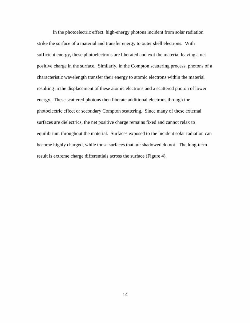
In the photoelectric effect, high-energy photons incident from solar radiation
strike the surface of a material and transfer energy to outer shell electrons. With
sufficient energy, these photoelectrons are liberated and exit the material leaving a net
positive charge in the surface. Similarly, in the Compton scattering process, photons of a
characteristic wavelength transfer their energy to atomic electrons within the material
resulting in the displacement of these atomic electrons and a scattered photon of lower
energy. These scattered photons then liberate additional electrons through the
photoelectric effect or secondary Compton scattering. Since many of these external
surfaces are dielectrics, the net positive charge remains fixed and cannot relax to
equilibrium throughout the material. Surfaces exposed to the incident solar radiation can
become highly charged, while those surfaces that are shadowed do not. The long-term
result is extreme charge differentials across the surface (Figure 4).

15
Figure 4. Physical processes resulting in surface charge differentials in a plasma environment. Photoelectric and Compton Effects result in positively charged surfaces through production of secondary electrons (upper). Stripping interactions result in positively charged surfaces exposed to plasma (lower) [12].
Stripping interactions that take place between the charged surface and the plasma
act as a compounding mechanism. The neutral plasma consists of electrons and positive
ions. If a surface is exposed to solar radiation, it becomes charged as described above;
when shadowed, it becomes negative. Plasma particles act to compound these charging
effects by stripping electrons from the exposed surface material in a manner similar to
what occurs on Earth when one shuffles across carpet at low humidity [11]. Low-density,
high-energy plasmas result in greater surface charge buildup. Consequently, the plasma
density and duration of surface exposure to solar radiation determines the degree to
which a surface is differentially charged. Satellites with components permanently
oriented toward the sun, or those in a stationary orbit with respect to the sun and those

16
located in high energy plasma environments, have much greater potential for surface
charging and subsequent ESD [12].
Not only can dielectric surfaces present large potentials across homogenous
materials, they can also differentially charge over much smaller scales. Satellites’
external surfaces generally comprise numerous materials. Each material presents
different secondary and photoelectron currents, resulting in numerous surface potentials.
These varying potentials can result in discharge across or through a surface as the
materials attempt to equilibrate potentials [11]. Once the potential difference across the
surface exceeds the ability of the material to contain it, the material breaks down,
releasing the stored charge and relaxing to equilibrium. This threshold is known as the
breakdown potential or breakdown field (VBR [kV/cm]). This prolonged build-up of
charge can result in an ESD coupling to critical internal spacecraft components. These
discharges can result in device failure, component burn-out, system reset, or, in some
cases, catastrophic failure of the entire vehicle.
2.1.3 Simulating Space Radiation Induced Damage Mechanisms in Dielectrics
A recent test conducted by the French aerospace lab ONERA replicated the
surface-charging space environment. ONERA used a distribution of 10-400 keV
electrons at a current density of 0-2 nA/cm2 to replicate the typical charging environment
during high solar activity. The irradiation cross-section diameter was 200 mm, and the
tests were conducted at temperature ranges of -190 to +150˚C at a constant vacuum of 10-
6 hPa. This test facilitated the characterization of in-situ discharges as well as the ability
to measure the radiation-induced conductivity of the test materials [18]. While large
chamber testing over a wide distribution of electron energies is useful for validating

17
satellite construction, geometry, and ESD failure mechanisms, it is not always ideal for
isolating electrical phenomena in the bulk with regard to damage mechanisms.
Subsequently, in this current work, electron energy distributions are much narrower and
sample size is smaller to better isolate the change in electrical properties of interest.
In this thesis, surface charging is replicated through the employment of MIL-STD
1541 ESD test practices. The space environment, specifically the electron radiation
environment, is replicated through use of the Wright State University’s Van de Graaf
(VDG) electron accelerator. Since the primary purpose of this research is to examine the
damage mechanisms within nickel nanostrandTM-infused composites, the radiation
environment must be one that facilitates radiation penetration deep within the test sample.
The VDG provides this ability to select a precise energy distribution with a known
penetration range.
The three predominant byproducts of energy transfer between incident electron
radiation and materials are ionization, excitation, and atomic displacement [19]. When
an energetic particle strikes a material, two interactions can result in energy loss;
electronic energy loss (ionization) and non-ionizing energy losses. Electronic energy loss
occurs when electrons are removed from the associated nuclei. This mechanism results
in vibration within the lattice, light emission, or an electrical current. Ionizations can
occur many times as the electron transits the material, resulting in an ionization cascade,
and high transient currents can arise [20].
Contrastingly, non-ionizing energy losses (NIEL) result in atomic displacements
within the lattice. In this mechanism, atoms are “knocked” from their stable location
within the material if the energy transferred from the incident particle is greater than the

18
displacement energy (Ed) binding the atom to its neighbors in the material. The vacancy
at the atom’s previous location and the interstitial where the atom re-attached to the
lattice are termed a Frenkel pair (Figure 5). NIEL radiation can generate numerous
Frenkel pairs depending on both the incident particle energy and the binding energy of
the lattice [20]. For each atomic species in a material or composite there is a threshold
incident particle energy below which atomic displacements do not occur. This threshold
for electrons in composites is generally between 100 and 300 keV [20].
Figure 5. Two primary electron-material interaction mechanisms: Ionization (left), and NIEL -displacement damage (right) [22].
Damage produced in conductors and semiconductors can anneal over time or with
increased temperature. This effect returns the material to a configuration closer to its pre-
radiation state. Dielectric materials do not anneal as easily as do conductors, hence
defects tend to remain for longer periods of time. These defects, when compounded in a
continuous radiation stream, can significantly alter the electrical properties of the
material, specifically reducing conductivity [21].
The classical measure of energy transfer to a material is given by the Bethe
formula (Equation (1)). This formula describes the specific energy loss due to collisional
19
losses (ionization and excitation) for fast electrons [34]. The total energy lost is a
combination of the collisional losses plus the radiative losses. Radiative losses are
minimal in nickel-carbon nanocomposites due to the relatively low atomic number of the
constituents as well as the relatively low energy of the incident electrons.
( ) ( ) ( ) ( ) ( )
4 2 22 2 2 20
2 2 20
2 1ln ln 2 2 1 1 1 1 182 1
where
c
dE e NZ m v E eVdx m v cmI
vc
π β β β ββ
β
− = − − − − + − + − − −
≡
(1)
In Equation (1), E is the kinetic energy of the incident electron, β is the ratio of electron
velocity to the speed of light, I is the experimentally determined average excitation and
ionization potential, N and Z are the number density and atomic number of the absorber
atoms, m0 is the electron rest mass, and e is the electron charge. This equation is used in
the analysis portion of this thesis to describe the electron energy deposition in nickel-
carbon nanocomposites as a function of range through the material.
2.1.4 Nanocomposites and Associated Electrical Properties
Nickel nanostrandsTM are fabricated via a Low Temperature, Atmospheric
Pressure Chemical Vapor Decomposition (LTAPCVD) process [23]. This process has
only been accomplished in batch mode to date, due to the unique needs of the Department
of Defense (DoD) customers, but is expandable to large-scale fabrication.
The benefits of nickel are numerous. As a magnetic metal, nanostrands can be
aligned similar to any ferromagnetic fiber. They provide a degree of chemical activity
and can serve as a catalyst or absorption material. These uses have not been researched
or tested to the extent that the electrical properties have been demonstrated.

20
The historical method of increasing the conductivity of a material is the addition
of an electrically conductive material in the form of a particulate coating or thin film
application [23]. The drawback to these methods is the relatively low aspect ratio, which
requires higher added fractions and, ultimately, much greater weight. In terrestrial
applications this is generally of little concern. However, in aerospace applications, where
weight is a primary design concern, nanostrands offer a much reduced weight when
compared to coating techniques, resulting in opportunities for increased payload weight
and reduced launch cost.
Some alternatives to nickel nanostrandsTM that similarly increase conductivity and
reduce weight do exist. Two of these are carbon nanotubes and carbon nanofibers.
While these materials do display increased electrical properties to coatings and films,
they are limited in their mechanical rigidity and the preferential molecular orientations of
carbon. As well, these materials are difficult to manufacture and much more expensive
than nickel-based nanofibers [23].
Nickel nanostrandsTM are created as a porous mesh (lattice). The mesh can then
be mixed in a resin base or can be compressed to a specific density or configuration. This
latter method, termed a “veil” keeps the nickel lattice intact, and generally results in
much greater conductivity (Figure 6) [23].
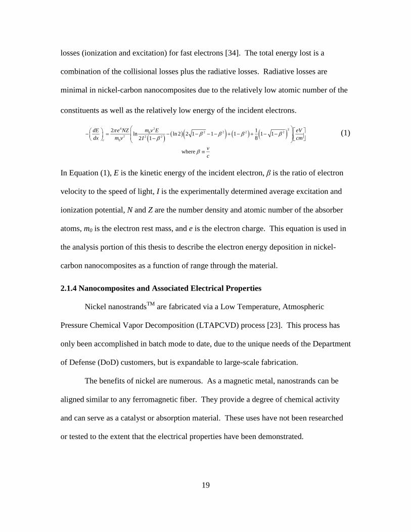
21
Figure 6. Volume resistivity of two methods of nickel nanostrandTM production: mixing the nanostrands into the liquid resin and adding resin to lattice intact. Note the significant increase in resistivity in the mix configuration [23].
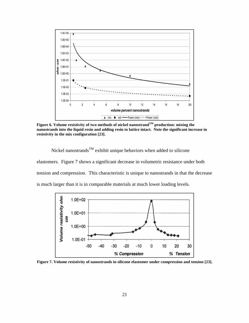
Nickel nanostrandsTM exhibit unique behaviors when added to silicone
elastomers. Figure 7 shows a significant decrease in volumetric resistance under both
tension and compression. This characteristic is unique to nanostrands in that the decrease
is much larger than it is in comparable materials at much lower loading levels.
Figure 7. Volume resistivity of nanostrands in silicone elastomer under compression and tension [23].

22
Nanostrands also provide a mechanism to control the electrical properties of
carbon composites. Adding a low loading of nanostrands to a dielectric-like composite or
one with low conductivity creates pathways of current flow within the composite.
Nanostrands have a tendency to fill voids previously occupied by the epoxy resin in the
composite. This loading method capitalizes on the strength characteristics of the
composite but also makes it fully conductive. Additionally, this method facilitates
engineering specific conductivity in the material as well as the orientation of the
associated fields [23]. Figures 8 and 9 show that the small fraction of added weight
associated with adding nanostrands to the composite to achieve a desired conductivity
greatly, outperforms the weight that would be required for a thin film coating with similar
conductivity.
Figure 8. Comparison of conductivity for nanostrands™ in resin (left), and the amount of nickel coating on a carbon fiber (right) [7].
23
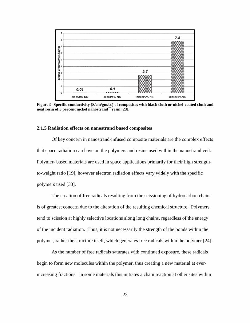
Figure 9. Specific conductivity (S/cm/gm/cc) of composites with black cloth or nickel-coated cloth and neat resin of 5 percent nickel nanostrand™ resin [23].
2.1.5 Radiation effects on nanostrand based composites
Of key concern in nanostrand-infused composite materials are the complex effects
that space radiation can have on the polymers and resins used within the nanostrand veil.
Polymer- based materials are used in space applications primarily for their high strength-
to-weight ratio [19], however electron radiation effects vary widely with the specific
polymers used [33].
The creation of free radicals resulting from the scissioning of hydrocarbon chains
is of greatest concern due to the alteration of the resulting chemical structure. Polymers
tend to scission at highly selective locations along long chains, regardless of the energy
of the incident radiation. Thus, it is not necessarily the strength of the bonds within the
polymer, rather the structure itself, which generates free radicals within the polymer [24].
As the number of free radicals saturates with continued exposure, these radicals
begin to form new molecules within the polymer, thus creating a new material at ever-
increasing fractions. In some materials this initiates a chain reaction at other sites within

24
the polymer; at other times, it is a one-to-one reaction. Regardless of the mechanism, the
free radicals cause the initial polymer to chemically change over time, thereby altering its
electro-mechanical properties [24].
Little research has been done regarding the use of nickel nanostrandsTM infused
into polymeric-based composites from a space radiation perspective [23]. The AFRL/RX
has recently flown configurations of these materials on the International Space Station as
part of the Material International Space Station Experiment (MISSE) for the purpose of
specifically determining the effect of free radicals in polymeric reconfiguration (Figure
10) [26]. Additional samples are scheduled to fly on MISSE 7, with launch scheduled for
early 2009.
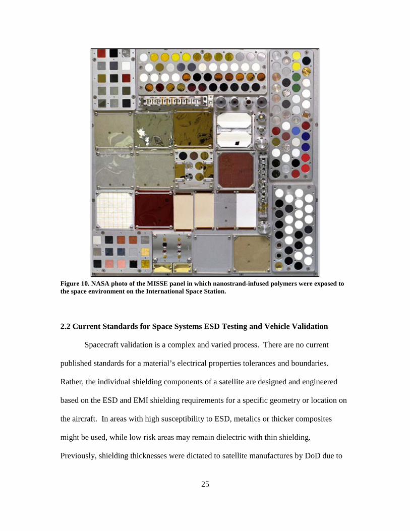
25
Figure 10. NASA photo of the MISSE panel in which nanostrand-infused polymers were exposed to the space environment on the International Space Station.
2.2 Current Standards for Space Systems ESD Testing and Vehicle Validation
Spacecraft validation is a complex and varied process. There are no current
published standards for a material’s electrical properties tolerances and boundaries.
Rather, the individual shielding components of a satellite are designed and engineered
based on the ESD and EMI shielding requirements for a specific geometry or location on
the aircraft. In areas with high susceptibility to ESD, metalics or thicker composites
might be used, while low risk areas may remain dielectric with thin shielding.
Previously, shielding thicknesses were dictated to satellite manufactures by DoD due to

26
computational modeling limitations and nascent metallurgical and composite fabrication
methods. However current designers are given greater freedom due to modeling and
simulation advances. This trend allows greater flexibility in material choice and
thickness yet makes validation of a single composite material difficult without full
understanding of its location and purpose on a satellite [40].
While no standard or regulation currently dictates the required material and
electrical properties of composites for satellite use, recent collaboration between AFRL
and a preeminent national aerospace corporation has determined an appropriate upper
bound for external satellite surface bulk resistivity to be 0.5 Ω-cm. It is believed that this
upper bound will suffice as a maximum resistivity for nickel-carbon nanocomposite use
in the current satellite design effort under way [41]. While this resistivity threshold is
believed to be sufficient from an EMI shielding perspective, it is unclear whether this
limit holds for ESD mitigation.
ESD test practices for composite-built space vehicles have not been standardized
to date, primarily due to constant evolution in material properties and space vehicle
fabrication techniques. The migration from conductive alloys, common from NASA’s
inception through the mid 1980s, to current polymerized composites and nanotechnology
has resulted in a lack of broad-based standardization. Regardless of these circumstances,
NASA’s published test practices and technical papers provide insight and clarification to
the baseline standard of the late 1980s, the most impacting of which is MIL-STD-1541A,
Electromagnetic Compatibility Requirements for Space Systems [15-17]. This document
outlines the general approach to ESD testing, as well as the type of ESD simulators and
pulse parameters best suited for space applications.

27
Three primary ESD tests apply to replicating the discharge associated with
surface charging. Radiated field tests provide a means for determining the surface’s
propensity to discharge onto externally mounted scientific instruments. More commonly
termed the air discharge test (ADT), this test is conducted with a voltage source held
some distance away from the surface. The surface is repeatedly charged with the voltage
source at a pre-determined pulse rate and the subsequent discharge is measured [17].
Most critical to this research, the single-point discharge test, or contact discharge
test (CDT), is conducted with the voltage source in contact with the surface and an arc
current return wire or probe in close proximity to the surface to capture the transmitted
ESD traversing the surface. This test is commonly descretized over the test surface to
identify and map out areas susceptible to repeated discharge. Of importance in
conducting CDT is the consideration of edge effects on the surface, where material
parameters are non-homogenous. Penetrating radiation can cause additional damage to
the structure at discontinuities and joints, thus making those locales more susceptible to
discharge [17].
NASA further dictates how the application of the CDT should be employed and
the test criteria of primary interest. The following criteria apply to all space vehicle
surfaces exposed to radiation in orbits above 8000 km or any orbit above 40 degrees
latitude [16].

28
NASA specifies the following focus areas as the minimum parameters of interest
when conducting ESD testing in accordance with MIL-STD-1541:
(1) Spark location (discharge point)
(2) Radiated fields or surface structure currents
(3) Area thickness and dielectric strength of the material
(4) Total charge involved in the event
(5) Breakdown voltage
(6) Current waveform: risetime, falltime and rate of rise [A/sec]
(7) Voltage waveform: risetime, falltime and rate of rise [17].
Note: Of these criteria, this research focuses primarily on: (1), (3), (4),
and (6).
Further, NASA advises that the space-based ESD generator (the real ESD) be
replicated in testing with the MIL-STD-1541 arc source, or a similar device which
conforms to those ESD properties listed below in Table 2. For comparison, the
commercially purchased ESD3000 discharge device is listed as an alternative to the MIL-
STD-1541 arc source (Table 2, (3)).

29
Table 2. ESD Characteristics for (1) In-Space Event, (2) MIL-STD-1541 Arc Source, and (3) ESD3000 Commercial System [15].
ESD Event ESD Mechanism
Capacitance (C) [nF]
Energy (E) [mJ]
Peak Current (Ip) [A]
Discharge Current Rise
Time (tr) [ns]
Discharge Current Pulse
Width (tp) [ns]
(1) Dielectric Discharge in Space
Dielectric to Conductive Substrate
20 10 2 3 10
(2) Complex Circuit
MIL-STD-1541
Auto Coil 0.035 6 80 5 20
(3) Commercial
System
ESD3000 w/ DN4
Discharge Module
0.5 4-6 100 0.7-1.0 8
In conducting the ESD test, MIL-STD-1541 gives the following directives [15]:
(1) Equipment (test specimen) shall not exhibit anomalous behavior or degradation when subjected to the test (6.1.1).
(2) The test setup shall simulate the operational wiring and grounding scheme (6.7.2)
(3) For synchronous (geosynchronous) orbits, a pulsed discharge, at a pulse rate of 1 per second for a period of 30 seconds, shall be established at a level of 10 kV and a distance of 30 cm from each exposed face of the test sample (6.7.2)
(4) The test shall be repeated using a direct discharge from one test electrode to each top corner of the test sample for equipment exposed to the direct space environment (6.7.2.a)
(5) If the test sample fails below 10 kV, the voltage is to be decreased to the lowest failure threshold and noted.
(6) Test should be conducted in a controlled atmosphere with relative humidity at 30 percent. Note: For this research, directives (3) and (5) were not evaluated. Directive (3) is used to analyze the materials susceptibility to ESD from an externally charged array or conductor. Directive (5) is used for qualification of surface failure.

30
The standard quantifies vehicle surface material ESD test failure as a discharge
that exceeds 10 kV through the surface (directive 5 above). Those materials that do not
discharge prior to this threshold are considered validated from a single-point ESD
perspective, however this only qualifies the material under test, not the entire system.
Therefore, the 10 kV failure threshold was not evaluated in this research because the
materials tested herein required discharge voltages well above the 10 kV threshold. The
pulsed air discharge test (directive 3 above) was not conducted on this material due to the
small sample sizes used as well as time and equipment limitations.
2.3 The ESD Discharge Pulse and Parameters of Interest
All materials contain charged particles which interact with electromagnetic fields
incident on or through the material. When these particles move or align under an applied
field, currents form in the material to return it to a charge-neutral state [37]. The ability
for these charges to move within a material is determined by the material’s permittivity
and conductivity.
Permittivity is the quantity used to describe field effects on dielectric materials
and is determined by a material’s ability to polarize (align charge) under the incident
field. When a field is applied through the bulk of the dielectric material, in this case a
large potential difference delivered by the ESD simulator, the bound charges in the
composite lattice align with the electric field, thereby polarizing the bulk. The composite
material can be viewed in this condition as a modified parallel plate capacitor with the
typical air gap replaced with a dielectric composite. The electric flux density within the
composite bulk, D, is proportional to the permittivity of free space, ε0 [F/m], multiplied

31
by the magnitude of the incident electric field, Ea, plus the magnitude of the polarization
vector, P resulting from the field (Equation (2)) [37].
0 2
where
a
net
CD E Pm
P q
ε = + =
(2)
A more convenient form of Equation (2) is expressed by associating the amplitude
of the polarization vector, P, with the applied field (Equation (3)) [37]. In this
formulation the permittivity of free space, ε0, is incremented by the dimensionless
quantity, χe, the electric susceptibility, which describes the ease of which a dielectric
polarizes.
0
0
where (1 )1and
s a
s e
ea
D E
PE
εε ε χ
χε
== +
=
(3)
In this form, εs is the static permittivity of the material [F/m]. Permittivity is more
commonly referenced as relative permittivity given by the ratio of static permittivity
divided by that of free space, or simply the dielectric constant of the material, εr.
Conductivity, σs, is the metric that describes the degree to which electrons can
move within a material and can change through numerous mechanisms such as
temperature variation or damage to the atomic structure. When an electric field is applied
to a material, electrons drift in the direction of the field at the velocity, ve, determined by
their mobility in the material, µe, and the strength of the field, Ea. This moving charge
gives rise to a conduction current density, Jc, within the material, which is a function of
the total charge multiplied by the velocity of the charge, ve. By Equation (4),

32
conductivity is then a function of the electron charge density within the material and the
mobility of that moving charge.
2
Given that ,
and ,
gives ,
therefore .
e e a
c e e
s a
s e e
mv Es
AJ q vm
J ESqm
µ
σ
σ µ
= − =
=
= −
(4)
These electrical properties for dielectric composites under test are used to analyze
the three characteristic parameters of interest in this research: ESD pulse rise time, tr;
pulse decay time to 50 percent of peak current, tf50; and peak discharge current, Ip.
Both the rise time and decay time of an ESD pulse within a material are
determined by its conductivity and permittivity. A highly resistive material is
characterized by a low number of conduction electrons within the material and low
charge mobility [39]. Materials of this type require more time for the incident field to
liberate electrons from the lattice and to begin moving them within the material.
Contrastingly, highly conductive materials characteristically have high electron mobility
and a near-infinite supply of free electrons, thus rise and decay times are comparatively
much shorter.
Decay time is the measure used to determine a material’s charge neutralizing
capability through the bulk of the material and is generally more telling of the
mechanisms of change within a material [38]. Charge neutralization occurs when the
material under test is in contact with charge carriers of the opposite polarity, in this case
the injected charge from the ESD device tip. The field induced by the ESD pulse causes

33
the carriers within the bulk to move. The movement of these charges to the discharge
return probe superimposes an opposing field over the induced field, resulting in a
decaying total field in the system [38]. Combining elements from Equations (3) and (4)
and solving the time dependent differential equation for charge density, D, shows that the
charge relaxation time constant, or decay time, tf, is a function of the material permittivity
and resistivity (Equation (5)) [38].
0
Given that ,
and ,
and ,
therefore ( ) ,
and [ ].
s
s
as
sc s a
s
c
t
sf
s
DE
DJ E
dDJdt
D t D e
s
σε
εσ
σε
ετ
σ
−
=
= =
−=
=
=
(5)
The effect of altering the permittivity and/or the conductivity of a material is a
broadening or narrowing of the ESD current pulse through the change in pulse decay time
(tf50). As the ratio of these parameters increases, more time is required to return the
material to a charge neutral state. The byproduct of peak broadening is a decrease in
peak current, Ip, measured through the dielectric material.
2.4 Summary
The unique space environment in which nickel-carbon composites will be
employed is harsh and unforgiving. As such, this research focuses on replicating the
damaging mechanisms of 500 keV space radiation and evaluating the long-term
34
propensity of numerous nickel-carbon configurations to serve as a viable alternative to
metallic satellite structures.
This research compares the surface and bulk resistivity of composites prior to and
following electron radiation. Further, electrostatic discharge testing is used to examine
the change in peak discharge current and the timing characteristics of the discharge
waveform to gain insight into the locus and mechanisms of damage interactions within
the composite and its constituents.
35
III. Methods of Experimentation
3.1 Introduction
This chapter outlines the methodology employed to analyze the composite
materials examined in this research. Specifically, it details the material configurations
and the three tests used to characterize material behavior prior to and following electron
irradiation.
3.2 Evaluated Materials
Metal Matrix provided eight composite configurations with nickel nantostrandTM
concentrations varying in placement, density, and method of incorporation into the
material. These eight configurations are grouped into three distinct composite types with
each configuration itemized below in Table 3.
Table 3. Specifics of sample configurations showing matrix and resin type, nickel nanostrandTM concentration and method of infusion.
Composite Group
Sample Configuration Carbon Matrix Resin Base Nickel
Concentration
Method of Nickel
Infusion
1 A AS4-3K (6-ply) PTMW A None NA
B AS4-3K (6-ply) PTMW A
174 gsm total (external surfaces)
Surface Laid Veil
C AS4-3K (6-ply) PTMW A 242 gsm total Interwoven
2 M M55J (8-ply) RS-3 1 x 200 gsm layer (mid-plane) Veil
I M55J (8-ply) RS-3 4 x 50 gsm layers (inter-laminar) Veil
Ext M55J (8-ply) RS-3
2 x 100 gsm layers
(external surfaces)
Surface Laid Veil
3 D Graphite Base (2050) None
260 gsm (external surfaces)
Surface Laid Thin Film Laminate
E Graphite Base (2050) None None NA

36
Consisting of configurations A, B and C, composite group number one is
composed of a six-ply weave of AS4 matrix in a standard 0/45/90 degree lay-up with
PTMW aero epoxy. Metal Matrix provided nickel nanostrandTM concentrations of zero,
242 and 260 grams per square (gsm) for configurations A, B, and C, respectively.
Configuration B has surfaced-laid nanostrand deposition on both exterior surfaces at 121
gsm, for a total of 242 gsm for the bulk material. Configuration C differs in that the
nanostrands are interwoven into the epoxy resin uniformly distributed throughout the
composite. Figures 11-13 show a cross-sectional view of configurations A through C,
respectively.
Figure 11. Configuration A, no nickel, 5 x magnification.
37
Figure 12. Configuration B, 242 gsm nickel, 5 x magnification (note approximately 50µm nickel layers on external surfaces).
Figure 13. Configuration C, 260 gsm nickel interwoven throughout the bulk, 5 x magnification.
Consisting of configurations M, I and Ext (Mid-plane, Inter-laminar and
Exterior), composite group number two is composed of an eight-ply weave of M55J
38
matrix in a standard 0/45/90 degree lay-up with RS-3 space-grade epoxy. Each
configuration has a total nickel nanostrandTM concentration of 200 gsm. The mid-plane
(M) configuration has one layer of nickel located between the carbon layers along the
transverse centerline of the bulk. The inter-laminar configuration (I) has four 50 gsm
nickel layers located at equidistant levels between the surfaces. The exterior
configuration has two 100 gsm nickel layers located on the exterior surfaces of the bulk.
Figures 14 through 16 show a cross-sectional view of configurations M, I and Ext,
respectively.
Figure 14. Configuration M (Mid-plane), 200 gsm nickel located centerline (note the 200 µm nickel layer).

39
Figure 15. Configuration I (Inter-laminar), 200 gsm nickel (note four distinct layers of 50 gsm nickel evenly dispersed).
Figure 16. Configuration Ext (Exterior), 200 gsm nickel (note approximately 100µm nickel on external surface).

40
Composite group three consists of configurations D and E. These configurations
have a thin graphite base. Configuration E has no nickel, while configuration D has 87
gsm nickel nanostrandTM located on both exterior surfaces for a total nickel concentration
of 174 gsm. Figures 17 and 18 show a cross-sectional view of these two configurations.
Figure 17. Configuration D, 174 gsm nickel on surfaces (note solid graphite bulk).

41
Figure 18. Configuration E, no nickel, graphite bulk only.
Sample number D2 (configuration D, one-inch disk number two), was maintained
throughout all pre and post-irradiation measurements as the control sample. This sample
was used to confirm equipment calibration prior to each measurement, thereby insuring
repeatability and continuity through measurement cycles.
3.3 Test Specimen Preparation
For bulk resistivity and ESD testing, a minimum of five, one-inch circular disks
were cut from each configuration plate using a CNC high-precision water jet with less
than 0.002 in variation in sample diameter. Two-hundred angstrom depositions of
aluminum and gold contacts were vapor deposited on two samples of each configuration
to facilitate bulk resistivity measurements (Figure 19) by ensuring uniform contact
between the probe surface and the composite surface and significantly reducing contact
resistance over the rough surface of the composite.

42
Figure 19. One inch diameter disk samples showing (left to right) four-point 200 Å gold deposition, 200 Å aluminum deposition (used in bulk resistance tests) and sample without contacts (used in ESD testing).
For surface resistivity measurements, three 2 cm x 0.210 cm test samples were cut
from the bulk sheets using a high-precision CNC water-cooled diamond saw. Samples
were heated and affixed to the cutting surface via a wax melt. Samples were re-heated
after cutting and residual wax was removed via absorption towels.
All samples were cleaned prior to each test using a wash solution consisting of
10% by volume fraction Acetone in doubly de-ionized water. This removed residual
wax, oil and metallics deposited on the surface through the cutting and handling process.
3.4 Surface Resistivity Measurements
Surface resistivity, ρs, is a measure of a material’s opposition to the flow of
current across the surface. A low resistivity is indicative of increased charge mobility.
This is highly desirable from a spacecraft surface charging perspective. Increased
mobility and low resistance allow charge to distribute over larger areas and reduce the
likelihood of ESD. The generalized equation for resistivity [ρs] is given in Equation (6)
43
as the resistance in ohms [Ω] multiplied by the ratio of surface area to depth of current
penetration within the material, termed the effective length.
[ ]sAR cmd
ρ = Ω− (6)
Surface resistivity measurements were made using a Keithley 4200 Semi-
conductor Characterization System via the Keithley Interactive Test Environment
software (KITE). Samples were mounted in an AFRL-fabricated four-point probe test
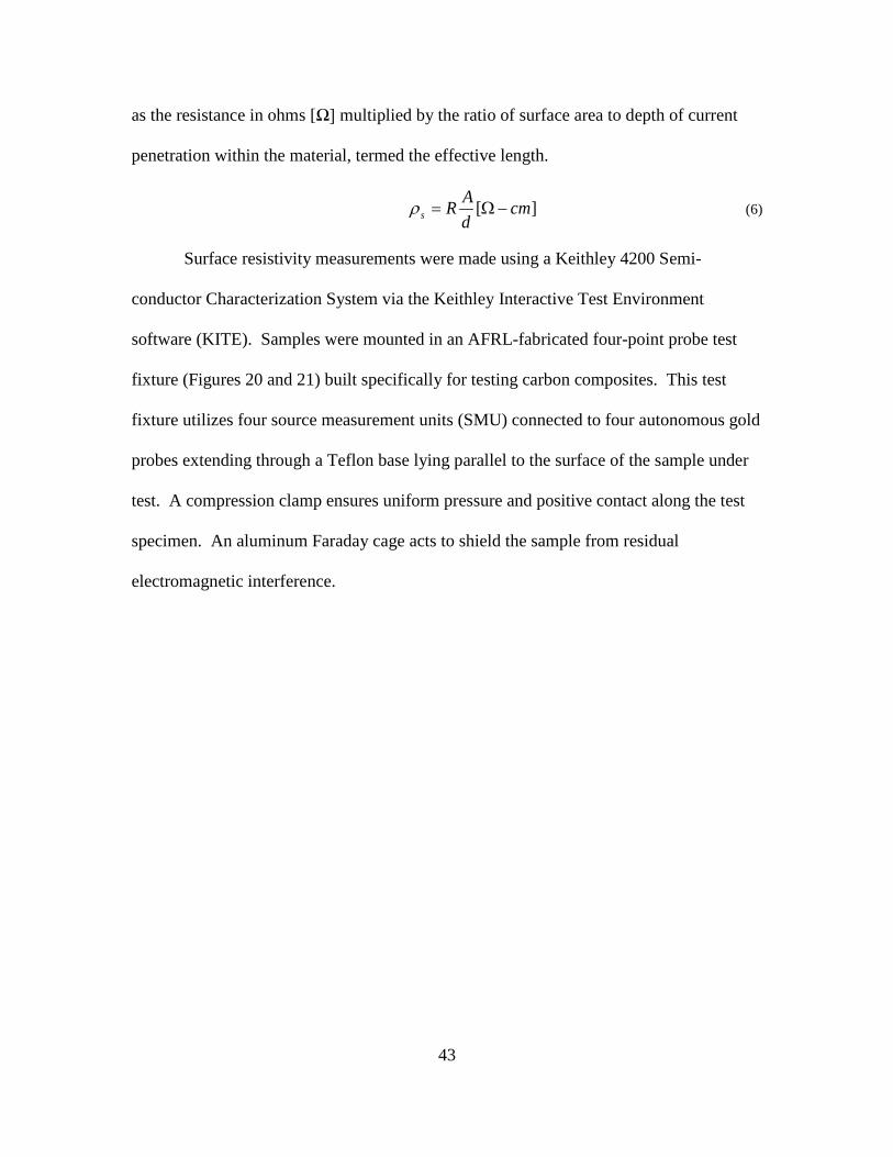
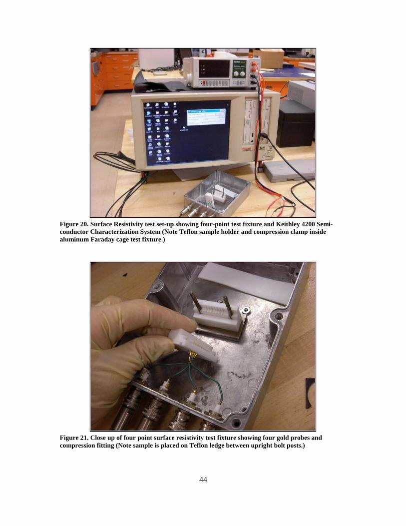
fixture (Figures 20 and 21) built specifically for testing carbon composites. This test
fixture utilizes four source measurement units (SMU) connected to four autonomous gold
probes extending through a Teflon base lying parallel to the surface of the sample under
test. A compression clamp ensures uniform pressure and positive contact along the test
specimen. An aluminum Faraday cage acts to shield the sample from residual
electromagnetic interference.
44
Figure 20. Surface Resistivity test set-up showing four-point test fixture and Keithley 4200 Semi-conductor Characterization System (Note Teflon sample holder and compression clamp inside aluminum Faraday cage test fixture.)
Figure 21. Close up of four point surface resistivity test fixture showing four gold probes and compression fitting (Note sample is placed on Teflon ledge between upright bolt posts.)

45
Probe number one sources current, probes two and three measure voltage drop
across the surface of the sample and probe number four is connected to common ground.
Unique to this measurement is the reduction of contact resistance common to dielectric
samples measured under low current conditions using a two-probe configuration, in
which the resistivity is measured through the same probe that sources the current.
The resistance of the material surface determines the depth of penetration of
equipotential lines below the surface. As indicated in Figure 22, the higher the surface
resistance, the deeper the charge penetrates the material as it transits to the grounded
probe and the longer the effective length the charges must travel. The result is a larger
voltage difference measured across probes three and four, and an increased resistance as
determined by Ohm’s law.
Figure 22. Cross-sectional view of surface resistivity test showing difference in equipotential line penetration into the surface based on the resistance of the surface layer. The top image shows high resistance layer, bottom image shows low resistance surface resulting in longer and shorter effective length respectively.
46
The software was configured to source current from -10 mA to 10mA in one µA
increments, alternating positive and negative current with two measurements at each
current. Measurements were taken at a three-second sweep delay followed by a three-
second hold time to allow current relaxation across the surface between measurements.
Sample resistivity is determined using Ohm’s Law (Equation (7)) via the slope of the
voltage difference [∆V] versus sourced current [I] plot.
[ ]VRI∆
= Ω (7)
Effective length was determined by entering the measured width and thickness of
each sample into an executable program specific to the four-point test fixture used.
Three test samples of each configuration were each measured three times for a
total of nine pre-radiation characterization measurements for each configuration used for
comparison to the irradiation samples created later in the experiment.
An example of current-verses-voltage difference curves with associated error
bars are shown below (Figure 23) for the interlaminar configuration (I). The slope of this
curve, multiplied by the effective length of each sample, gives the sample surface
resistivity. These pre-irradiation measurements are itemized below in Table 4.

47
Figure 23: Example resistance curves for the three interlaminar (I) configuration samples. Plotted for each sample is the mean of the three measurements and the associated ± 5 percent measurement error. The nine individual measurements are almost indistinguishable which validates the consistency and reapeatability of the measurement.
Figure 24 shows the mean current verses voltage difference curves for all
configurations; the greater the slope, the higher the sample surface resistivity.
Configuration A with no nickel is the most resistive and configuration D with 184 gsm
nickel nanostrands™ on the external surfaces of a thin graphite wafer is the most
conductive. Configurations M, I and Ext of composite group two all have similar surface
resistivity.

48
Figure 24. Plot of Mean Current vs. Voltage Difference curves for all sample configurations. Slope of curve determines resistance by Ohm’s Law. Configuration A has greatest surface resistance, Configuration D is the most conductive, and resistance generally decreases with increased nanostrand™ content.
Table 4. Pre-Radiation Mean Surface Resistivity for three test samples of each configuration shown in order of decreasing resistivity.
Configuration Mean Resistivity [mΩ-cm] 1-σ [mΩ-
A 30.3 ±0.8
C 25.6 ±1.8
B 22.9 ±0.5
Ext 20.0 ±0.2
I 13.9 ±0.1
E 12.5 ±0.8
M 12.5 ±1.2
D 10.6 ±0.3

49
3.5 Bulk Resistivity Measurements
Pre-irradiation bulk resistivity measurements were made to characterize the bulk
material properties perpendicular to the orientation of the composite ply. These
measurements were made using a Keithley 2700 Digital Multimeter/Data Acquisition
Switching System (DMM). Measurements were recorded via GPIB interface to a laptop
computer running ExcelinkTM Visual Basic for Excel software. The software recorded
bulk resistance in three-second sweep and hold-time intervals.
The test fixture used in this measurement consisted of a 0.5 in copper disk
inserted into the bottom of a high-density polyethylene (HDPE) sleeve with a 1.5 in
hollow core. The sample under test was placed inside the hollow sleeve resting on the
top of the copper disk with the 200-Å aluminum contact facing up. A one-pound
stainless steel (ASTM standard) compression weight was placed into the hollow sleeve to
provide uniform compression atop the sample. The IEC 801.2 standard did not provide a
method to stabilize the compression weight during the measurement which resulted in
measurement variations. This variability was reduced through the use ASTM
compression weight and HDPE sleeve which provided uniform compression across the
sample surface and reduced the average measurement error by an order of magnitude.
Two four-point FLUKE probes were affixed to the top of the steel compression
weight and to the wire lead exiting the copper disk. Figures 25 and 26 show detail of the
bulk resistivity test set-up and test fixture used.

50
Figure 25. Bulk resistivity test set-up showing test fixture, Keithley 2700 DMM and laptop with Keithley Excelink interface.
Figure 26. Detailed view of bulk resistivity test fixture showing high density polyethylene sleeve, one-inch copper disk with contact wire feed through, ASTM standard compression probe and four-point test leads connected to Keithley DMM (not shown).

51
Samples were measured by removing and re-inserting the compression probe for
each measurement interval. A minimum of 30 measurements were taken over a 90-
second interval for each sample under test. Two samples of each configuration were
tested. Bulk resistance was converted to resistivity (ρ) via Equation (6), where A is the
surface area of the sample under test, d, is the thickness of the sample, and R is the
measured resistance.
Figure 27 depicts the pre-irradiation bulk resistivity with associated one standard
deviation (1-σ) error bars for samples of each configuration. These measurements show
that for each sample set, those configurations with nickel nanostrands™ on the external
surfaces (Configurations B, D and Ext) have lower bulk resistance than those
configurations with nickel located internal to the sample (Configurations C, I and M).
Configurations A and E are carbon composite and graphite respectively with no nickel,
and are the most resistive of the respective composite groups. Configuration M, with 200
gsm nickel nanostrands™ located along the midplane is the most resistive configuration at
an average of 13.7 Ω-cm.
Of note in this analysis is the lack of bulk resistivity data for sample I2, Ext2 and
M2. These samples had excessive epoxy on the external surfaces due to use in previous
experiments. As a result, the associated resistances for these samples were exceedingly
high and are not representative of accurate pre-irradiation material properties.
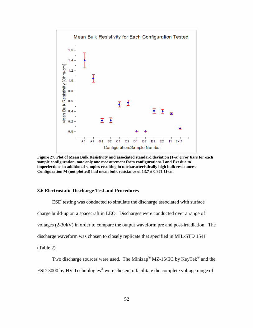
52
Figure 27. Plot of Mean Bulk Resistivity and associated standard deviation (1-σ) error bars for each sample configuration, note only one measurement from configurations I and Ext due to imperfections in additional samples resulting in uncharacteristically high bulk resistances. Configuration M (not plotted) had mean bulk resistance of 13.7 ± 0.871 Ω-cm.
3.6 Electrostatic Discharge Test and Procedures
ESD testing was conducted to simulate the discharge associated with surface
charge build-up on a spacecraft in LEO. Discharges were conducted over a range of
voltages (2-30kV) in order to compare the output waveform pre and post-irradiation. The
discharge waveform was chosen to closely replicate that specified in MIL-STD 1541
(Table 2).
Two discharge sources were used. The Minizap® MZ-15/EC by KeyTek® and the
ESD-3000 by HV Technologies® were chosen to facilitate the complete voltage range of

53
the ESD discharges of interest. The Minizap was used primarily to conduct ESD tests
below 12 kV and the ESD-3000 was used for discharges between 12 kV and 30 kV.
Figures 28 and 29 show the standard test configuration and equivalent circuit used
for the ESD simulation, respectively. The ESD simulator was charged to the desired
output voltage with the pointed discharge tip placed on the sample (contact discharge)
prior to triggering the discharge. The discharge return ground lead was connected to the
ground output of the SDN-414-025 Current Viewing Resistor (CVR). The sample under
test was placed onto the copper test plate electrically isolated on the high-density rubber
brick. The copper test plate was connected to the CVR to complete the current loop. The
CVR was connected to the oscilloscope using a standard B&C connector. Output
waveforms were captured using a Tektronix® TDS5100B digital oscilloscope. In order to
adequately capture the complete waveform for high-voltage discharges (above 16 kV),
Tektronix x2, x5, and x10 attenuators were used to reduce the current multiplication on
the oscilloscope.

54
Figure 28. ESD test set-up showing MiniZap® discharge source, Tektronix® TDS5100B oscilloscope (w/ typical 8kV waveform), Tektronix x2, x5, and x10 signal attenuators, SDN-414-025 current viewing resistor, sample under test rests atop a 2x2 inch copper plate mounted on a high density rubber brick.
Figure 29. Equivalent Circuit for ESD testing showing ESD generator (Minizap® MZ-15/EC), device under test, current viewing resistor and oscilloscope.
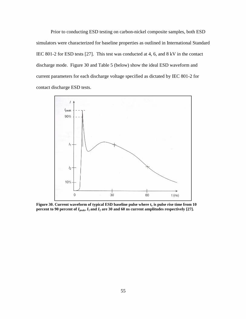
55
Prior to conducting ESD testing on carbon-nickel composite samples, both ESD
simulators were characterized for baseline properties as outlined in International Standard
IEC 801-2 for ESD tests [27]. This test was conducted at 4, 6, and 8 kV in the contact
discharge mode. Figure 30 and Table 5 (below) show the ideal ESD waveform and
current parameters for each discharge voltage specified as dictated by IEC 801-2 for
contact discharge ESD tests.
Figure 30. Current waveform of typical ESD baseline pulse where tr is pulse rise time from 10 percent to 90 percent of Ipeak, I1 and I2 are 30 and 60 ns current amplitudes respectively [27].
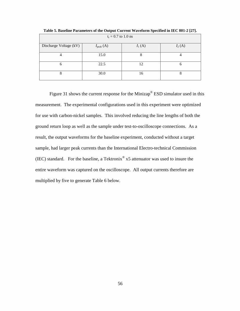
56
Table 5. Baseline Parameters of the Output Current Waveform Specified in IEC 801-2 [27]. tr = 0.7 to 1.0 ns
Discharge Voltage (kV) Ipeak (A) I1 (A) I2 (A)
4 15.0 8 4
6 22.5 12 6
8 30.0 16 8
Figure 31 shows the current response for the Minizap® ESD simulator used in this
measurement. The experimental configurations used in this experiment were optimized
for use with carbon-nickel samples. This involved reducing the line lengths of both the
ground return loop as well as the sample under test-to-oscilloscope connections. As a
result, the output waveforms for the baseline experiment, conducted without a target
sample, had larger peak currents than the International Electro-technical Commission
(IEC) standard. For the baseline, a Tektronix® x5 attenuator was used to insure the
entire waveform was captured on the oscilloscope. All output currents therefore are
multiplied by five to generate Table 6 below.

57
Figure 31. 4, 6, and 8 kV five-point average smoothed discharge waveforms from Minizap® ESD simulator for baseline comparison against EIC 801-2 test standards. Note: Waveforms are the mean of 30 discharge measurements at each voltage.
Table 6. Baseline parameters of the Output Current Waveform for Minizap® under ESD test configuration used in this experiment.
tr = < 0.4 ns
Discharge Voltage (kV) Ipeak (A) I1 (A) I2 (A)
4 16.2 3.8 2.9
6 25.9 5.3 4.5
8 32.6 6.5 5.0
Tables 5 and 6 show that for the test configuration in this research, I1 and I2 are
significantly lower than the IEC 801-2 standards. The IEC 801-2 standard was developed
to test industrial systems in which discharges are replicated via the human body model.
The discharge mechanism in this research simulates the discharge waveform from the
human body to the equipment under test. The first pulse (narrow) is representative of the
58
charge dissipated through the material under test from the human hand. The second pulse
(wide) represents the charge dissipated through the material via the human body [31].
However, while the pulse duration and peak current are very similar, the 30 and 60 ns
currents are higher in the IEC standard due to the necessity in most experimental set-ups
to use long cables and large grounding planes to facilitate testing of large pieces of
equipment. The simplified small-scale test set-up used in this measurement more
efficiently captures the first peak current discharge, thereby reducing the latent pulse
amplitude not witnessed in the IEC 801-2 model.
While the two test set-ups differ in late-time current amplitude, both waveforms
are similar in duration and peak current, thereby validating this test method for use in
ESD evaluation of carbon-nickel composite samples.
Evaluation of the ESD waveform for each sample under test (SUT) required a
minimum of 30 discharge measurements for each discharge voltage increment (2,4,6,8,
and 12 kV). The data were then analyzed in OriginLab® 7.5 software. The mean
waveform of the 30 measurements for each voltage increment was used as the primary
data for further analysis, an example of which is below (Figure 32).

59
Figure 32. Sample plot of mean waveform from 30 ESD measurements at 8 kV on configuration B sample (Note: The waveform is smoothed).
Figure 32 shows a representative ESD current waveform following discharge
through a nickel-carbon test sample (in this case configuration B). All associated
discharges for all configurations showed similar pulse shape and duration. Notable
characteristics of the pulse are a fast rise to a peak current (within the first 2 ns of the
pulse), which quickly decays to a lower threshold (between 7-10 ns) then rises again and
decays away slowly over approximately 90 ns.
The ESD waveform is inherently noisy due to both the energy and speed of the
pulse. As such, pulses displayed throughout this thesis are smoothed using adjacent
averaging to aid in the analysis. The error reported on each chart is the error associated
with the mean pulse prior to smoothing, and will be shown in one of two ways: 1) on the
60
chart at peak current, 30 and 60 ns (as in Figure 32); or 2) in the legend for charts with
multiple waveforms included. In general, pre-irradiation measurements are shown in red
and post-irradiation measurements are in blue. Due to the high resolution in plotted data
(20 picoseconds per point) waveforms are displayed as a line rather than individual data
points.
3.6.1 Electrostatic Discharge Current Equations
The genesis of the accepted ESD discharge current model originates from that of
measured lightning discharge current (Equation (8)) [27, 28]. In this formulation, i0 is the
peak current and t1 and t2 are time constants describing the associated rise and fall time of
the current pulse.
( ) 1 20
t tt ti t i e e− −
= − ⋅ (8)
The first approximation of the ESD current discharge was given by Cerri et al. as the
double exponential function in Equation (9) [29].
( ) 1 21 2
t tt ti t i e i e− −
⋅ ⋅= − (9)
Further revisions by Berg et al. in 1998 gave Equation (10), the sum of one narrow and
one broad time based Gaussians [32]. This equation best describes the ESD pulse in
early time, within the first ten nanoseconds.
( )2 2
1 2
1 2
t t t t
i t A e B t eσ σ − −
− − = ⋅ + ⋅ ⋅ (10)

61
Equation (11), the most representative model for the ESD pulse following the initial peak
was formulated in 2003 by Wang et al. based on the lightning current equation given by
Heidler [30, 31].
( ) 2 4
131 2
2 1
133 4
4 3
33
311 23 3
1 2
1 3
3
1
3
2
wher
1
n
1
e
a d
t ttt
i ii t e ek kt t
k e
k e
τ τ
τ ττ τ
τ ττ τ
ττ
τ τ
− −
−
−
= ⋅ ⋅ + ⋅ ⋅
+ +
=
=
(11)
In both Equations (10) and (11), time (t) is measured in nanoseconds and begins upon the
initial rise of the first peak.
For the purpose of this research, Equations (10) and (11) are used to analyze the
ESD pulse prior to and following irradiation. Equation (10) is used to determine the time
constants of the narrow peak in early time, and Equation (11) is used to analyze the late
time behavior of the discharge pulse.
3.6.2 Current Pulse Analysis via Genetic Algorithms
Genetic Algorithms (GA) are adaptive search techniques used to find solutions to
complex equations involving a large search space often populated with multiple local
minima and maxima. The ESD current waveform is ideally suited to this method, as the
experimental data is both noisy and covers an expansive current range over a small time
scale.
Genetic Algorithms were born from evolutionary biology research. The GA is
based on the principles of reproduction, cross-over and mutation used to converge at an
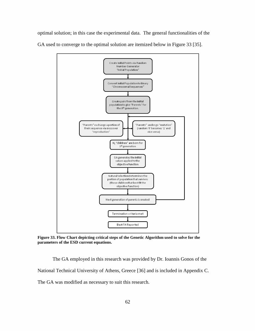
62
optimal solution; in this case the experimental data. The general functionalities of the
GA used to converge to the optimal solution are itemized below in Figure 33 [35].
Figure 33. Flow Chart depicting critical steps of the Genetic Algorithm used to solve for the parameters of the ESD current equations.
The GA employed in this research was provided by Dr. Ioannis Gonos of the
National Technical University of Athens, Greece [36] and is included in Appendix C.
The GA was modified as necessary to suit this research.
63
The output of the GA gives the parameters of the best fit between the ESD current
waveform equation (Equations (10) and (11)) and the experimental data, the fitting of
which is determined by either a pre-set number of generations or an error tolerance. The
primary exit criteria used in this research was generation number, the number of fitting
iterations between parents and children. The metric used to determine the fit of the GA
generated parameters to the experimental data is a summation of the difference between
measured current and the optimized current divided by the measured current, and is
termed Fg, where is the ith value of the experimental current, is the ith value of the
GA determined current, and N is the total number of evaluated time increments (Equation
(12)).
1
m cNi i
g mii
I IF
I=
−= ∑ (12)
A comparative example of the GA fit to the experimental data is shown in Figure
34. This depicts the correlation between the experimental data from a typical ESD
current waveform and the best fit to the data using Equation (11), the Heidler equation for
ESD discharge. The GA determined parameters of Equation (11) are shown inset on the
chart.

64
Figure 34. Comparison of the Experimental Data (blue) from 12 kV ESD on Ext sample to the GA-determined fit (red) using Equation (11) (Heidler Equation). Maximum error is ±0.2 A at Ip for experimental data.
The GA was applied to experimental data collected prior to and post-irradiation
for all configurations. Analysis was conducted on the 12kV discharge current waveforms
to determine the parameters to the ESD equation.
Once the best-fit equation was determined via the GA, simple manipulation
facilitated the analysis of the pulse with regard to three critical parameters: pulse rise time
(tr), peak current (Ip) and pulse decay time to 50 percent of Ip (tf50).
3.7 Electron Irradiation Procedures
The LEO space environment to which materials similar to those tested in this
experiment are exposed throughout a life-cycle was simulated using the High Voltage
Engineering, Europa, Electron Van de Graaf generator (SN-A94)(Figure 35).
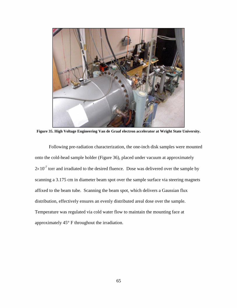
65
Figure 35. High Voltage Engineering Van de Graaf electron accelerator at Wright State University.
Following pre-radiation characterization, the one-inch disk samples were mounted
onto the cold-head sample holder (Figure 36), placed under vacuum at approximately
2×10⁻⁷ torr and irradiated to the desired fluence. Dose was delivered over the sample by
scanning a 3.175 cm in diameter beam spot over the sample surface via steering magnets
affixed to the beam tube. Scanning the beam spot, which delivers a Gaussian flux
distribution, effectively ensures an evenly distributed areal dose over the sample.
Temperature was regulated via cold water flow to maintain the mounting face at
approximately 45° F throughout the irradiation.

66
Figure 36. AFIT standard “cold head” sample mount with cold water inlet and outlet connected. The one-inch disk sample is mounted on fore face.
3.7.1 Electron Energy Selection
Prior to determining the target electron energy used in this experiment, a Monte
Carlo simulation of electron trajectories in solids, termed CASINO® v2.42, was used to
explore both the range and energy relationships of electron radiation in the configurations
under test.
In concert with the CASINO® code, MIL-STD 1809 was used to select the typical
energy range of the most damaging electron radiation in LEO. Finally the National
Institute for Standards and Technology (NIST) database was used to confirm that the
range of these electrons was sufficient to access the areas of interest in the configurations
under test. The ideal energy range for these samples based on analysis of the above three
resources was determined to be between 250 and 450 keV.

67
Figure 37 is an example of the CASINO® output used to determine the energy
distribution of 500 and 1000 keV electrons in simulated samples similar to configurations
B, D, and Ext in this experiment. The simulated sample in CASINO® has a nickel
density equivalent (by thickness) to that of configuration Ext of composite group number
two. This image shows the bulk of the energy deposited at approximately 80% into the
bulk for the 500 keV simulation and much deeper (i.e. in the substrate after transiting the
sample under test) in the 1000 keV simulation. Figures 38 and 39 show similar
depictions of electron deposition in simulated samples. In Figure 38 with a simulated
electron energy of 500 keV, the predominance of the electrons come to rest inside the
sample bulk; contrastingly in Figure 39, the 1000 keV electrons come to rest in the
aluminum substrate outside the sample bulk.
Figure 37. Electron energy deposition CASINO® simulation of Ni-C-Ni configuration using 500 keV and 1000 keV electron irradiation. Note the 500 keV simulation shows the electron range coincident with sample thickness, whereas the 1000 keV simulation shows a much longer range and energy deposition occurring primarily within the aluminum shielding surrounding the sample.

68
Figure 38. CASINO® simulation of Ni-C-Ni configuration using 500 keV electrons, showing electron penetration depth within the sample bulk.
Figure 39. CASINO® simulation of Ni-C-Ni configuration using 1000 keV electrons, showing electron penetration depth outside the sample bulk into the aluminum substrate.

69
In an effort to maximize the electron-induced damage mechanisms in the samples
under test, 500 keV was determined to be the requisite upper threshold for these
irradiations, with a target energy of 400 keV due to the voltage and current limitations of
the Van de Graaf generator.
Comparing the CASINO® output to NIST’s online database shows a close
correlation. From the continuous slowing down approximation (CSDA) used by NIST,
the average range of a 500 keV electron is 0.1993 g/cm2 [33]. The average density of
amorphous carbon, of which the test samples resembles, is 1.82 g/cm3. Dividing the
CSDA range by the carbon density gives an average projected range of 1.095 mm, which
is approximately the thicknesses of the samples under test (variable from 0.95 to 1.65
mm) and closely matches the CASINO®-simulated range of 80 percent sample thickness.
3.7.2 Dosimetry Calculations
MIL-STD 1809 Space Environment for USAF Space Vehicles states that vehicles
should be designed to sustain all operational characteristics at a flux of 8×10⁶
[particles/cm2-sec] in environments wherein particle energy is at or above the 500 keV
threshold [14].
This equates to approximately 1016 [particles/cm2] total electron fluence over a 35
year life-cycle by the below Equation (13):
6
162 2
3658 10 60sec 60 min 24 35 1 10minsec
daye hr eyrhr day yrcm cm
− − ×⋅ ⋅ ⋅ ⋅ ⋅ ≅ × −
(13)
The following operating parameters were used on the VDG electron generator:

70
[ ] [ ]
[ ]
[ ] [ ]
6
162
22
2 10
1 10
2.08
[ ] 3.3984
Target Electron Current I Amps
eDesired Fluence Dcm
Diameter of Beam d cm
dArea of Beam Spot A cmπ
−
−
= ×
= ×
=
= =
Current Density was determined by Equation (14) to be 5.886 x 10⁻⁷ [Amps/cm2]:
[ ] 72 5.886 10I ACurrent Density J
A cm− = = ×
(14)
The electron flux for the operating parameters specified above for the VDG was
then determined by dividing the Current Density [J] by the charge of the electron
(Equation (15)).
( ) 1219 23.679 10
1.6 10 [ ] secJ eFlux D t
C cm
−
−
= = × × −
(15)
With the target total fluence of 1 x 10¹⁶ [particles/cm2], the irradiation time is
determined by dividing the total desired fluence by the flux (Equation (16)). For the
above stated fluence, the irradiation time is approximately 45 minutes:
[ ] 3 2.718 10 sec 45.3min( )radDIrradiation Time t
D t= = × = (16)
An identical approach was followed to determine all radiation parameters used in
this experiment.
3.8 Summary
These experimental procedures were followed throughout the duration of this
research. All measurements were highly repeatable and sufficient data were recorded
throughout to mitigate error, both experimental and human, to a reasonable level.
71
IV. Results and Discussion
The following sections highlight the relevant data collected throughout this
experiment, focusing on pre and post-irradiation changes within the various
configurations. Each measurement or analytical process is noted separately. Due to both
the large amounts of data collected and number of samples tested, characteristic charts
are only shown for those configurations displaying the most dramatic changes following
irradiation. However, the accompanying tables summarize the data for all samples tested.
Of note, due to the number of irradiations required throughout this experiment and
irradiation iteration limitations on the VDG accelerator, no samples of configuration E
were irradiated. This minimizes the comparative analysis for sample group three
(configurations D and E) but does facilitate the comparison of configuration D to like
configurations in other sample sets (configurations B and Ext).
4.1 Bulk Resistance Results
The ideal satellite skin should show little, if any, change in bulk resistivity
following irradiation. From a spacecraft charging and ESD perspective, if a material
does exhibit change, a post-irradiation decrease in bulk resistivity is preferable to an
increase. A decrease in bulk resistivity yields faster charge relaxation throughout the
material, and the material is better able to distribute both built-up and injected (ESD)
charge over a larger volume.
Displayed in Figure 40 and Table 7 are comparative results of bulk resistivity pre
and post-irradiation. Sample set one (configurations A, B and C) all showed a decrease
in bulk resistivity following a total fluence of 1016 e-/cm2. Configuration D of sample set
three and all configurations of sample set two (configurations Ext, I and M) showed a
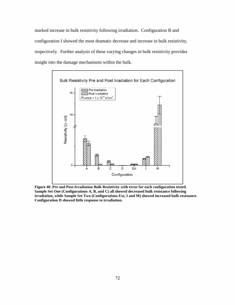
72
marked increase in bulk resistivity following irradiation. Configuration B and
configuration I showed the most dramatic decrease and increase in bulk resistivity,
respectively. Further analysis of these varying changes in bulk resistivity provides
insight into the damage mechanisms within the bulk.
Figure 40. Pre and Post-Irradiation Bulk Resistivity with error for each configuration tested. Sample Set One (Configurations A, B, and C) all showed decreased bulk resistance following irradiation, while Sample Set Two (Configurations Ext, I and M) showed increased bulk resistance. Configuration D showed little response to irradiation.

73
Table 7. Mean Bulk Resistivity Pre and Post-Irradiation showing relative change by percentage. Sample Set One showed decrease in bulk resistance post-irradiation, all others showed increase in bulk resistance.
Electron energies were maintained at 500 ± 10 keV for all irradiations, and the
location of the sample within the VDG beam spot remained constant throughout all
irradiations. Thus, the electron flux incident on each sample remained constant
throughout the irradiations. Further, the bulk resistivity test fixture measured within one
percent of the pre-irradiation baseline for the non-irradiated control sample (sample D2)
each time the fixture was used. With these factors consistent throughout the experiment,
it is safe to conclude that the experimental constraints discussed previously are not
responsible for the large changes in resistivity following irradiation. Variations in the
experimental procedures are small compared to the changes evident in table 7 and the
error associated with these variations are accounted for in the 1-σ standard deviation
noted. Therefore, the change in bulk resistivity is a result of radiation interactions within
the composite and not a result of measurement error or variations in the experiment.
Pre-Irradiation Post Irradiation Change
Configuration Mean Resistivity
1-σ [Ω-cm] Mean
1-σ [Ω-cm] %
A 1.40 0.15 1.15 0.12 -17.8
B 0.548 0.054 0.0689 0.0014 -87.4
C 0.215 0.037 0.0713 0.0094 -66.8
D 0.00684 0.00037 0.00798 0.00056 +16.5
Ext 0.0629 0.0098 0.0638 0.0099 +4.5
I 0.352 0.017 0.450 0.024 +27.3
M 13.2 0.672 14.9 0.81 +12.8

74
There is little correlation between samples with regard to both placement of the
nickel within the bulk or density of the nickel in the configuration. Configuration B, D
and Ext all have nickel located on the exterior surfaces. Configuration B had an 87
percent decrease in bulk resistivity, while both D and Ext showed 16.5 and 4.5 percent
increase respectively. Bulk resistivity in configuration B with 174 gsm external nickel
decreased greatly, while configurations D and Ext with 260 and 200 gsm external nickel
respectively increased.
Similarly, while not as precise a comparison as the external configurations, those
configurations with nickel located throughout the bulk (C, I and M), showed similar
behavior. Configuration C with 242 gsm Ni, which one would assume to be the least
resistive due to the even distribution of nickel throughout the composite, was more
resistive than both configurations D and Ext prior to irradiation. Following irradiation,
however, configuration C decreased by 66.8 percent, while configuration I and M both
increased in resistivity.
Consistent with expectations were configurations A and M. Configuration M
with nickel located in the mid-plane, and thus the greatest distance from the measurement
probes, was by far the most resistive, while configuration A with no nickel, was the
second most resistive sample.
The primary difference between sample set one and two is the epoxy resin used.
Sample set one uses PTMW aero epoxy, common to terrestrial systems. Sample set two
uses RS-3 space-grade epoxy. Since all configurations of each sample set displayed
similar post-irradiation change, it is concluded that in the bulk, the mechanism of change
must be due to the interaction between the electron radiation and the epoxy. While the

75
nickel certainly enables charge flow in those areas of the bulk in which it is concentrated,
the most impacting metric of change resides within the epoxy-matrix interaction.
Configuration Ext is the best composite material of those tested for use in space
from a bulk resistivity perspective. This composite shows the least change over a life-
cycle of damaging electron radiation. While the bulk resistivity in configuration Ext is
higher than other samples tested, its relative resistance to change in the bulk following
electron irradiation is preferable. Further, the configuration can be engineered to a lower
resistivity through the addition of more densely laid external nickel. Configuration D
also performed well in this measurement. Configuration D had the lowest bulk resistivity
both pre and post-irradiation., and while the relative change at 16.5 percent is greater than
configuration Ext at 4.5 percent, the measurement is an order of magnitude lower than
configuration Ext, thus the increase is insignificant. Configuration B showed significant
change however, from a charging perspective, the decrease in resistivity over time might
act to lessen the risk of ESD due to the material’s increased ability to dissipate charge
throughout the volume as it ages in space.
4.2 Surface Resistivity Results
Similar to bulk resistivity, the ideal satellite surface material should display little
change in surface resistivity following irradiation. Again, a decrease in surface resistivity
is preferable to an increase. Increased surface resistivity inhibits the surface’s ability to
distribute charge of a large area and increases the potential for ESD through the surface
and into critical components.
All configurations measured showed a marked increase in surface resistivity
following irradiation. Configuration Ext exhibited a 440 percent increase in surface

76
resistivity, the highest of any configuration (Figure 41). Configuration C only increased
by 79 percent, the lowest of those tested (Figure 42).
Figure 41. Pre and Post-Irradiation IV comparison with 1-σ standard deviation for Configuration Ext showing greatest increase (440 percent) in surface resistivity from 20.0 to 108 mΩ-cm.

77
Figure 42. Pre and Post- Irradiation IV comparison with 1-σ standard deviation for Configuration C showing lowest increase (76.9 percent) in surface resistivity from 25.6 to 45.3 mΩ-cm.
Figures 43 and Table 8 summarize the surface resistivity measurements. Similar
to the bulk resistivity measurements, the relative change in surface resistivity increase
coincides with the composition of the sample set. Configurations in sample set two (Ext,
M, and I) with RS-3 epoxy showed the greatest increase. Sample set one (A,B and C)
showed the least increase.
Prior to irradiation, configuration D was the least resistive, followed by sample set
two and one respectively, with configuration A being the most resistive as expected.
However following irradiation, those least resistive configurations showed the greatest
increase in surface resistivity.
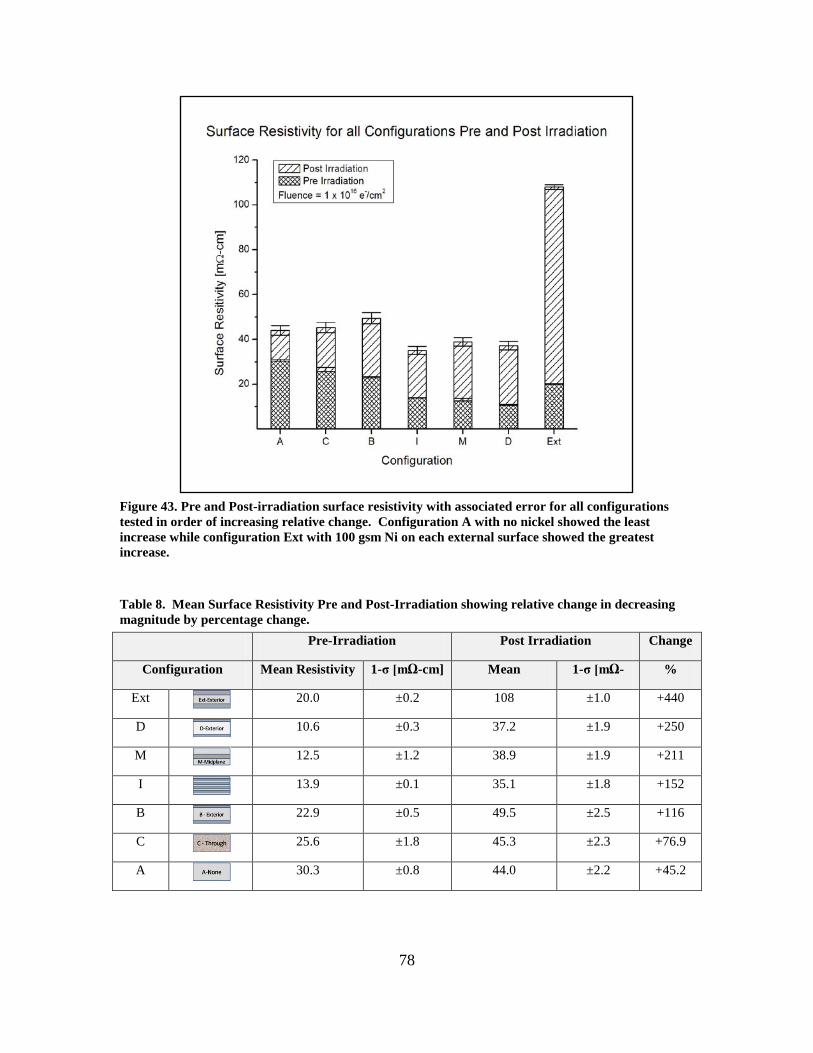
78
Figure 43. Pre and Post-irradiation surface resistivity with associated error for all configurations tested in order of increasing relative change. Configuration A with no nickel showed the least increase while configuration Ext with 100 gsm Ni on each external surface showed the greatest increase.
Table 8. Mean Surface Resistivity Pre and Post-Irradiation showing relative change in decreasing magnitude by percentage change.
Pre-Irradiation Post Irradiation Change
Configuration Mean Resistivity
1-σ [mΩ-cm] Mean
1-σ [mΩ-
%
Ext 20.0 ±0.2 108 ±1.0 +440
D 10.6 ±0.3 37.2 ±1.9 +250
M 12.5 ±1.2 38.9 ±1.9 +211
I 13.9 ±0.1 35.1 ±1.8 +152
B 22.9 ±0.5 49.5 ±2.5 +116
C 25.6 ±1.8 45.3 ±2.3 +76.9
A 30.3 ±0.8 44.0 ±2.2 +45.2

79
The location of nickel and nickel density do not seem to affect the surface
resistivity prior to irradiation. Configuration M with the nickel located the farthest from
the test fixture’s probes was less resistive than configuration Ext where the probes were
in closer proximity to the nickel.
Of configurations with similar nickel location, surface resistivity results varied
greatly. Configurations B and Ext have very similar external structures with
approximately 100 µm of external nickel. Following irradiation the Ext configuration
increased by more than 400 percent, while configuration B increased just 116 percent.
Those samples with nickel distributed throughout the bulk behaved similarly.
Configuration M showed a 211 percent increase, while C showed only a 76 percent
increase.
The common difference in the above trends is the epoxy used throughout the
sample sets. Sample set one (A, B and C) with PTMW aero epoxy showed the least
increase in surface resistivity, while sample set two (Ext, M and I) with RS-3 space grade
epoxy showed the greatest increase. While configuration D, with no epoxy, showed a
250 percent increase, it had the lowest pre-irradiation resistivity and the post-irradiation
measurement is consistent with most other configurations tested.
4.3 ESD Results
The 12kV ESD current waveform was used throughout this analysis. ESD
waveforms were measured in accordance with the experimental procedures. Shown
below in Figures 44 and 45 are the pre and post-irradiation mean waveforms for
configurations D and I, respectively. The primary post-irradiation changes noticed in this
research were in early-time peak current, and decay time of the early pulse. A decrease
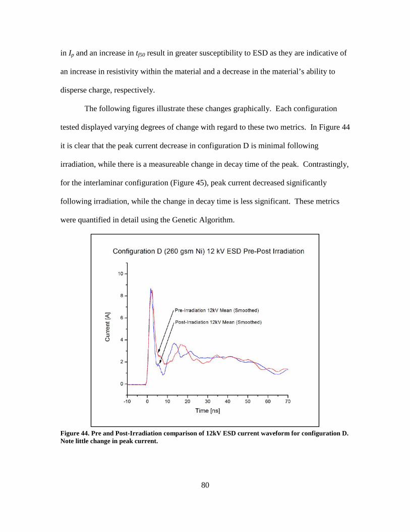
80
in Ip and an increase in tf50 result in greater susceptibility to ESD as they are indicative of
an increase in resistivity within the material and a decrease in the material’s ability to
disperse charge, respectively.
The following figures illustrate these changes graphically. Each configuration
tested displayed varying degrees of change with regard to these two metrics. In Figure 44
it is clear that the peak current decrease in configuration D is minimal following
irradiation, while there is a measureable change in decay time of the peak. Contrastingly,
for the interlaminar configuration (Figure 45), peak current decreased significantly
following irradiation, while the change in decay time is less significant. These metrics
were quantified in detail using the Genetic Algorithm.
Figure 44. Pre and Post-Irradiation comparison of 12kV ESD current waveform for configuration D. Note little change in peak current.

81
Figure 45. Pre and Post-Irradiation comparison of 12kV ESD current waveform for configuration I. Note significant decrease in peak current following irradiation.
4.3.1 Genetic Algorithm Solutions to ESD Equations in Early Time
Early time pulse characteristics were determined through analysis of the
experimental data and equation (10). The genetic algorithm was used to determine
equation parameters of the to compare pre and post-irradiation behavior in peak current
(Ip), pulse rise time, and the decay time to 50 percent of peak current (tf50). In this
analysis, the ideal material characteristics for these parameters would show minimal
change in the timing characteristics and peak current. An increase in decay time
coincident with a decrease in peak current correlate to an increase in resistivity within the
composite bulk.

82
The GA was employed over varying numbers of generations, parents, and
mutation and crossover rates to determine the best fit. The best fit was determined by
minimizing the total error (Fg) summed over the entire data range (see equation (12)).
Comparing the errors between GA iterations for each pulse facilitated the determination
of the best initial values for the individual pulse, thus establishing the equation used to
solve for those parameters of interest.
Figure 46 shows a typical best fit curve in early time (0-6 ns). The GA
determined parameters are shown inset. These values were then imported into a
Mathmatica® routine to solve for Ip, tr and tf50. This process was repeated for all
configurations pre and post-irradiation.
Figure 46. GA fit to experimental data for 0-6 ns ESD current waveform for Ext configuration using Equation (11). GA determined parameters are shown inset. Experimental error is ±0.2 A.
The early time characteristics of the pulse are representative of the initial contact
current injection of the Human Body Model as dictated by the RC circuit used in the ESD
simulator. The primary parameters used by the GA to compare the pre and post-
83
irradiation pulses in early time (below 10 ns) are t1 and t2 of the double Gaussian in
Equation (10). In this region, very small changes in these parameters can lead to large
changes in peak current. Since peak current is the metric of interest in early time,
Equation (10) provided a much better fit for this analysis than did Equation (11). This
equation better describes a broad pulse at lower amplitude.
Of significant importance in this analysis is the fact that these time constants
(parameters determined by the GA) are not the actual timing parameters (rise and decay
time) of the pulse. They correlate mathematically and are representative of the pulse time
characteristics but are simply a metric used to compare pre and post-irradiation effects
following their insertion into the ESD fitting equation. If each pulse were smooth, and
ringing and noise were not significant, the rise time and decay time of the early and late
portions of the pulse could be easily determined from the data. This, however, is not the
case for any pulse measured throughout this research. Thus, the GA provides a
reasonable means to remove these experimental anomalies and facilitated the comparison
of like pulses through the examination of the best-fit timing parameters.
Table 9 shows the early time pulse behavior and the relative change in each
following irradiation for each configuration. The 12 kV mean pulse data were used to
determine pulse rise time (tr), peak discharge current (Ip), and decay time to 50 percent of
peak current (tf50).
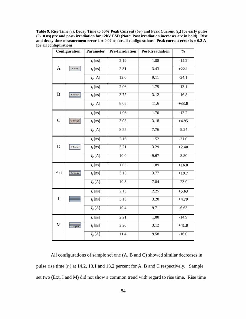
84
Table 9. Rise Time (tr), Decay Time to 50% Peak Current (tf50) and Peak Current (Ip) for early pulse (0-10 ns) pre and post- irradiation for 12kV ESD (Note: Post irradiation increases are in bold). Rise and decay time measurement error is ± 0.02 ns for all configurations. Peak current error is ± 0.2 A for all configurations.
Configuration Parameter Pre-Irradiation Post-Irradiation %
A
tr [ns] 2.19 1.88 -14.2
tf [ns] 2.81 3.43 +22.1
Ip [A] 12.0 9.11 -24.1
B
tr [ns] 2.06 1.79 -13.1
tf [ns] 3.75 3.12 -16.8
Ip [A] 8.68 11.6 +33.6
C
tr [ns] 1.96 1.70 -13.2
tf [ns] 3.03 3.18 +4.95
Ip [A] 8.55 7.76 -9.24
D
tr [ns] 2.16 1.52 -31.0
tf [ns] 3.21 3.29 +2.40
Ip [A] 10.0 9.67 -3.30
Ext
tr [ns] 1.63 1.89 +16.0
tf [ns] 3.15 3.77 +19.7
Ip [A] 10.3 7.84 -23.9
I
tr [ns] 2.13 2.25 +5.63
tf [ns] 3.13 3.28 +4.79
Ip [A] 10.4 9.71 -6.63
M
tr [ns] 2.21 1.88 -14.9
tf [ns] 2.20 3.12 +41.8
Ip [A] 11.4 9.58 -16.0
All configurations of sample set one (A, B and C) showed similar decreases in
pulse rise time (tr) at 14.2, 13.1 and 13.2 percent for A, B and C respectively. Sample
set two (Ext, I and M) did not show a common trend with regard to rise time. Rise time
85
increased 16 and 5 percent in configurations Ext and I, respectively, whereas
configuration M showed a 15 percent decrease in rise time. Rise time decreased by 31
percent for configuration D.
All configurations except B showed an increase in the decay time to 50 percent of
peak current (tf50). The relative change in decay time is not consistent within sample sets
or with regard to nickel placement. For example, configuration A, with no nickel,
showed a 22.1 percent increase following irradiation, while configuration C, with 242
gsm nickel, increased only 4.95 percent. Similarly, decay time for configuration D, with
260 gsm of external nickel, increased by 2.4 percent, while configuration Ext, with 200
gsm of external nickel, increased by 19.7 percent.
Peak current (Ip) decreased following irradiation for all configurations except B.
Again, there is no correlation between configurations of similar nickel placement or
density or between sample sets. In sample set one, configuration A, with no nickel,
showed a 24.1 percent decrease, while configuration C only decreased by 9.24 percent.
In configuration D, with 260 gsm external nickel, Ip decreased by only 3.3 percent, while
configuration Ext, with similarly placed external nickel decreased by 23.9 percent.
From the parameters analyzed in this measurement, configuration D proves to be
the best choice for satellite surfaces from an ESD perspective. Configuration D shows
the greatest resistance to post-irradiation change in the ESD current waveform. It showed
the smallest post-irradiation decrease in Ip at 3.3 percent and the smallest increase in tf50 at
2.4 percent, both of which show its comparative resilience to increased frequency and
intensity of ESD. Contrastingly, configuration Ext showed the poorest performance in
this measurement. Ip decreased by 23.9 percent, while tf50 increased by 19.7 percent.

86
These changes imply an increase in susceptibility to ESD both in frequency of occurrence
and in intensity. Configuration Ext is a poor choice for satellite surfaces based on its
ESD performance.
4.3.2 Genetic Algorithm Solutions to ESD Equations in Late Time
Late time current waveform analysis was better suited to Equation (11). This
portion of the ESD pulse is representative of the late current injection of the Human Body
Model following the discharge from initial contact (i.e. early time). As the pulse
deteriorates in current amplitude, significant ringing begins typically at about 15 ns.
Equation (11) provided a smooth fit to the data from this lower limit through the
completion of the measured data at 82 ns. This analysis facilitated examining the pulse
characteristics at 30 and 60 ns in accordance with IEC 801-2 standards for material
certification. While material certification is not the focus of this research, this
measurement further shows the applicability of the GA for use in certification if deemed
necessary during future research on these materials.
The late time current behavior was consistent for all configurations tested.
Figures 47 and 48 show the pre and post-irradiation comparison for the 12 kV waveform
for the Ext configuration.
Prior to irradiation, the 30 and 60 ns current measurements were 2.56 and 1.53 A,
respectively. Following irradiation, the current increased to 2.74 and 1.72 A,
respectively. These changes are consistent with early time behavior in which the peak
current decreased following irradiation. Since the total charge involved in the pre and
post-irradiation ESD is the same, and the current decreased in early time following
irradiation, the late time behavior is expected to increase in current amplitude as

87
witnessed in the Ext example here. This behavior was consistent throughout all
configuration measurements in late time.
Figure 47. Comparison between GA best fit to the experimental data for the 12 kV pre-irradiation ESD for configuration Ext. Error in the experimental data is ± 0.2 percent.
Figure 48. Comparison between GA best fit to the experimental data for the 12 kV post-irradiation ESD for configuration Ext. Error in the experimental data is ± 0.2 percent.
4.4 Measurement Summary
While there are few identifiable correlations between measurements with regard
to post-irradiation change based on nickel density, location or composite construction

88
type, the results do allude to significant changes across the configurations as a whole
following electron irradiation.
The ESD results show a decrease in Ip and an increase in tf50, resulting in a
broadening of the pulse in early time. By Equations (4) and (5) discussed previously, the
electrical properties responsible for this change are permittivity (ε) and conductivity (σ).
The degree to which each of these parameters changes following irradiation is difficult to
ascertain from the measurements made in this research, as both properties work in
concert to determine the charge holding capability of the material (decay time).
However, the data support some conclusions regarding the mechanisms of change within
the materials as a whole.
The electron energy used in this experiment was selected based on its expected
ability to induce displacement damage within the bulk of the composite. If the selected
500 keV electrons generated a significant number of displacement-induced Frenkel pairs
within the bulk, the result would be a decrease in electron mobility (µe) through the
carbon and epoxy lattices. As discussed previously (Equation (3)), a reduction in
electron mobility following irradiation would result in reduced conductivity (increased
resistivity) throughout the material. This effect was evident in the post-irradiation
increase in surface resistivity for every configuration measured, as well as in the bulk
resistivity increase in all configurations except sample set one.
Additionally, significant numbers of NIEL induced vacancies and interstitials
within the carbon lattice would result in a decrease in the magnitude of the polarization
vector (P) within the material bulk, as there would be fewer charges available to align
89
with the incident field (Ea) created by the ESD. The reduction of P would ultimately
reduce the material’s permittivity (Equation (3)).
Further, since there is no identifiable trend with regard to the nickel density or
placement, changes within the material which are manifested in the decrease in Ip and tf50
are likely due to the interactions between the electrons and the resin-carbon interfaces
within each configuration. Permittivity and conductivity likely change at different rates
for each configuration. Some configurations showed an increase in both resistivity
measurements as well as a decrease in peak current in the ESD measurements (Ext, I and
M), while others showed an increase in the bulk measurement (A, B and C).
It is also likely that the formation of free radicals within the epoxy results in
changes to both permittivity and resistivity differently based on the epoxy used. The
response to irradiation of the PTMW aero epoxy used in sample set one may differ
significantly from that of the RS-3 space grade epoxy used in sample set two. An
example of this is in the bulk resistivity measurements in which all configurations of
sample set one decreased in resistivity, while those of sample set two increased. In this
measurement, the effect of displacement damage caused within the carbon lattice, which
would act to increase the resistivity of the material, might be offset by conductive
pathways created in the bulk, as scissioning within the epoxy results in more conductive
hydro-carbon bonding. This effect is common in high-fluence ion-irradiation of
polymers, in which the radiation creates graphitization (the morphing of the polymer to
closely resemble graphite along the radiation track), which results in increased
conductivity within the material [42].

90
Regardless of the relative change in electrical properties between configurations
or the potential for conductivity to increase due to free radical formation within the
epoxy, all the composites tested in this research showed a decrease in the electric
properties as a whole, and are thus adversely effected by electron radiation. The result of
this decrease in electrical properties will likely subject the materials to increased
frequency and intensity of ESD when used in space.

91
V. Conclusion
This section begins with a review of the purpose of this research and a brief
summary of the experiments conducted on nickel-carbon nanocomposites. Then, final
conclusions are presented and explained. Finally, potential topics for future studies are
suggested.
5.1 Summary
The primary purpose of this research was to determine the effects of simulated
space radiation on the electrical properties of nickel-carbon nanocomposites and to
comment on their potential use as a external satellite skin. Of specific interest was each
material’s susceptibility to increased likelihood of electrostatic discharge resulting from
electron-induced damage mechanisms within the material. Further objectives of this
research were: to build and validate test fixtures and measurement techniques for future
work of this kind; to compare these materials’ performance against the NASA and DoD
standards for satellite surfaces; and to comment on the long-term use of nickel-carbon
nanocomposites as external satellite surfaces.
This purpose was achieved by conducting pre and post-irradiation surface and
bulk resistivity measurements and ESD discharge waveform analysis on seven different
nickel-carbon composites. Each configuration was evaluated following each of the three
measurements, and comparisons were made between sample sets to determine the best
performing configuration for each test.
5.2 Conclusions
From the analysis of the test results, the following conclusions can be drawn:
92
• Configuration D, with 260 gsm external nickel on a graphite base performs best of
all configurations tested. Configuration D meets the AFRL accepted 0.5 Ω-cm
bulk resistivity upper design threshold both pre and post-irradiation at 0.000684
and 0.00798 Ω-cm respectively and outperforms the next best configuration (Ext)
by an order of magnitude. Configuration D has the lowest pre-irradiation surface
resistivity at 10.6 mΩ-cm and although this measurement increases 250 percent
following irradiation to 37.2 mΩ-cm its post-irradiation surface resistivity is
consistent with all other configurations. Finally, configuration D far outperforms
all others tested from and ESD perspective. It showed only a 2.40 percent
increase in tf50 with a 3.30 percent decrease in tp, which alludes to comparatively
less propensity for increased ESD frequency and intensity when compared against
other configurations. Of note in this analysis is the lack of epoxy in configuration
D.
• Configuration M is the poorest choice for external satellite surfaces. Post-
irradiation bulk resistivity was four orders of magnitude higher than the best
performing composite (configuration D). Similarly, configuration M showed the
greatest increased in tf50 at 41.8 percent. These factors combine to yield a much
greater chance propensity for ESD intensity and occurrence through the material’s
lifecycle.
• Configurations B, C, D, Ext and I all meet the AFRL accepted 0.5 Ω-cm bulk
resistivity upper design threshold both pre and post-irradiation, however behavior
is not consistent between these configurations in surface resistivity and ESD
testing.

93
• If employed as an external satellite surface, all composites tested in this research
will degrade with time due to electron induced damage mechanisms. While some
perform better than others (as discussed above), these composites all show a
decrease in the ability to quickly distribute charge throughout the composite bulk
following irradiation. In space, surface charge densities will increase as the
composites age, and the material will ultimately discharge via ESD at lower
thresholds. This will lead to more frequent and energetic ESD through the surface
into critical internal components, or externally to critical arrays or antennae.
• The electrical properties of nickel-carbon nanocomposites degrade following
exposure to simulated space radiation. Regardless of whether a configuration
showed a significant increase in surface and bulk resistivity, each configuration
showed a decrease in critical parameters of peak current (Ip) and decay time (tf50)
in the ESD analysis. The early-time current pulses broadened following
irradiation, which means that the charge relaxation capability of the material
decreased. This points to the extreme likelihood that the materials will become
more susceptible to surface charging and subsequent ESD when exposed to long-
term space radiation.
• 500 keV electron radiation caused sufficient damage across the composite surface
to cause an increase in surface resistivity for all configurations tested.
• 500 keV electron radiation initiates changes within the composite bulk that alters
its conductivity. This resulted in an increase in bulk conductivity for
configurations A, B and C, and a decrease in conductivity for all other
configurations.

94
• Changes in the electrical properties of nickel-carbon composites cannot be
attributed to a given configuration’s nickel content or nickel placement within the
material. The experiments conducted in this thesis revealed no trends between
configurations of similar structure or nickel placement.
• Displacement damage likely occurs both within the epoxy resin and the carbon
matrix. These vacancies and interstitials likely reduce the material’s conductivity
through the reduction in electron mobility in the lattice. Additionally,
displacement damage may reduce the material’s ability to polarize under the ESD
field, thereby decreasing the permittivity of the composite.
• The choice of epoxy plays a role in the relative change in bulk resistivity
following irradiation. Configuration D with no epoxy outperformed all other
configurations in every measurement. Sample set one (A, B and C) with PTMW
aero epoxy showed a decrease in resistivity following irradiation, while all others
with RS-3 epoxy showed an increase in resistivity. The scissioning of long-chain
hydrocarbons resulting in the formation of free radicals within the epoxy may
result in the decreased resistivity seen in sample set one.
• The experimental procedures and test fixtures used in this research are validated
for further use in testing materials of this type.
5.3 Recommendations for Future Research
The most critical step in future analysis of these composite materials is the
determination of where the electron induced damage mechanisms occur and isolation of
the electrical property most affected by that damage. Electron paramagnetic resonance

95
(EPR) should provide insight into the locus and mechanisms of the changes itemized in
this thesis.
Additionally, further analysis of the epoxy-carbon interactions within the
composite is critical to determining whether the changes in conductivity and permittivity
are a result of displacement damage or a byproduct of free radical formation within the
epoxy. This could be achieved by repeating these experimental procedures on samples of
a common carbon base using different epoxies, or alternatively by examining the nickel-
epoxy interactions on glass without a carbon matrix.
The composites tested in this research were examined without fully taking into
account all the standards outlined in MIL-STD and NASA publications for validating
satellite materials. Future analysis should include the air discharge and pulse cycling
tests and determination of the breakdown voltage. This additional analysis might provide
additional insights into the long-term behavior of these materials in space, and are
necessary to fully vet the materials for future space use.

96
Appendix A: Genetic Algorithm
The below Genetic Algorithm was supplied by Dr. Ioannis F. Gonos of the
National Technical University, Athens, Greece, and is used with permission of said
institution and author. All files are MATLAB ‘.m’files and are located on the
AFIT/GNE/Thesis Hard Drive in BLDG 470.
Main Function (ganew.m):
%Genetic Algorithm %ESD Current %Function of I1, I2, t1, t2, t3, t4, n %Created by Ioannis F. Gonos 02-02-2005 %Files which are used: parents gagenia gafun clear; close all NumberOfParents=20; Bit=20; Variables=7; ChildrenNumber=4; ProbMutation=0.2; IterationNumber=20; dio=2^Bit-1; fid = fopen (' Output.txt',' w'); load B12kvPost.txt % change this to file to be analyzed Q=B12kvPost for j=1:NumberOfParents FirstParents=parents (NumberOfParents, Bit, Variables); for i=1:1 g=gagenia (FirstParents, Bit, Variables, ChildrenNumber, ProbMutation); f (i)=gafun (g (1,:), Bit, Q); FirstParents=g; end j par (j,:)=FirstParents (1,:); end FirstParents=par for i=1:IterationNumber g=gagenia (par, Bit, Variables, ChildrenNumber, ProbMutation); f (i)=gafun (g (1,:), Bit, Q); par=g; I1 = 0 + 40*par (1,1)/dio; I2 = 0 + 20*par (1,2)/dio; t1 = 0 + 3*par (1,3)/dio;
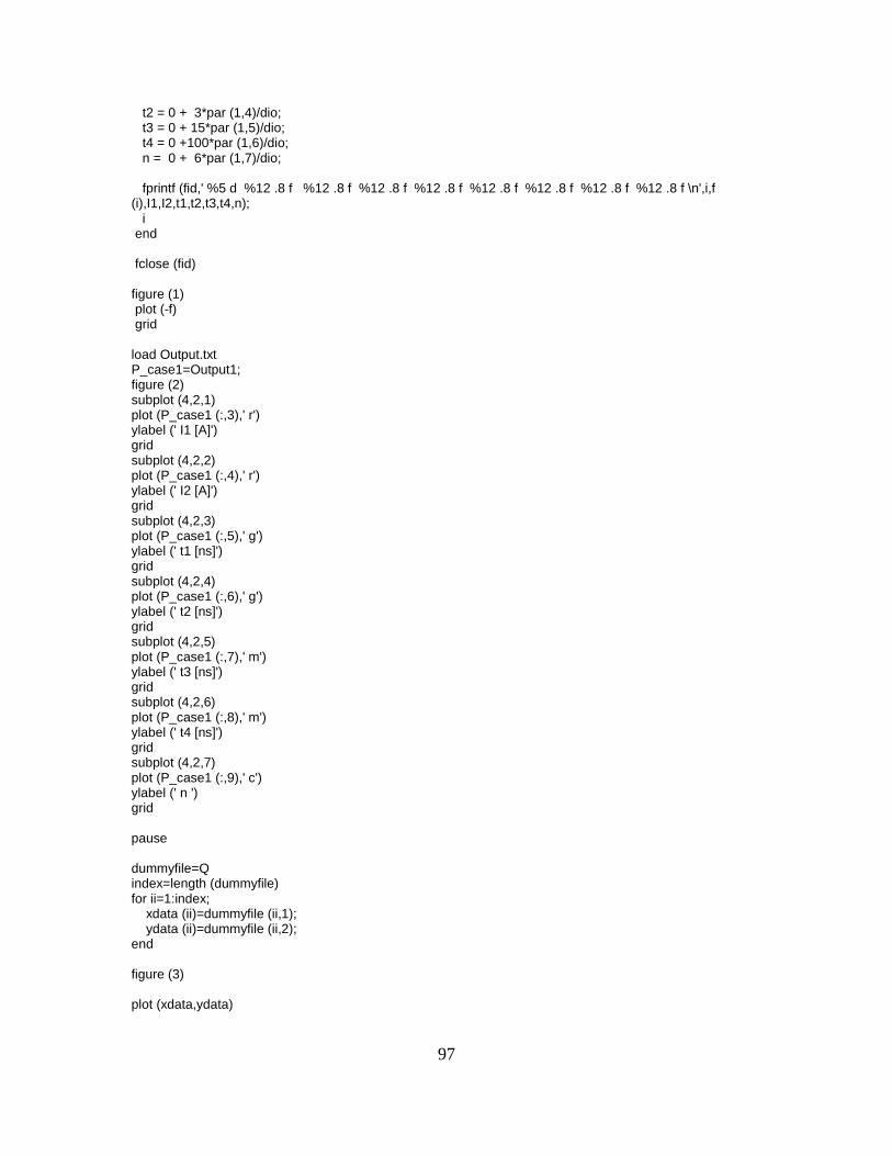
97
t2 = 0 + 3*par (1,4)/dio; t3 = 0 + 15*par (1,5)/dio; t4 = 0 +100*par (1,6)/dio; n = 0 + 6*par (1,7)/dio; fprintf (fid,' %5 d %12 .8 f %12 .8 f %12 .8 f %12 .8 f %12 .8 f %12 .8 f %12 .8 f %12 .8 f \n',i,f (i),I1,I2,t1,t2,t3,t4,n); i end fclose (fid) figure (1) plot (-f) grid load Output.txt P_case1=Output1; figure (2) subplot (4,2,1) plot (P_case1 (:,3),' r') ylabel (' I1 [A]') grid subplot (4,2,2) plot (P_case1 (:,4),' r') ylabel (' I2 [A]') grid subplot (4,2,3) plot (P_case1 (:,5),' g') ylabel (' t1 [ns]') grid subplot (4,2,4) plot (P_case1 (:,6),' g') ylabel (' t2 [ns]') grid subplot (4,2,5) plot (P_case1 (:,7),' m') ylabel (' t3 [ns]') grid subplot (4,2,6) plot (P_case1 (:,8),' m') ylabel (' t4 [ns]') grid subplot (4,2,7) plot (P_case1 (:,9),' c') ylabel (' n ') grid pause dummyfile=Q index=length (dummyfile) for ii=1:index; xdata (ii)=dummyfile (ii,1); ydata (ii)=dummyfile (ii,2); end figure (3) plot (xdata,ydata)
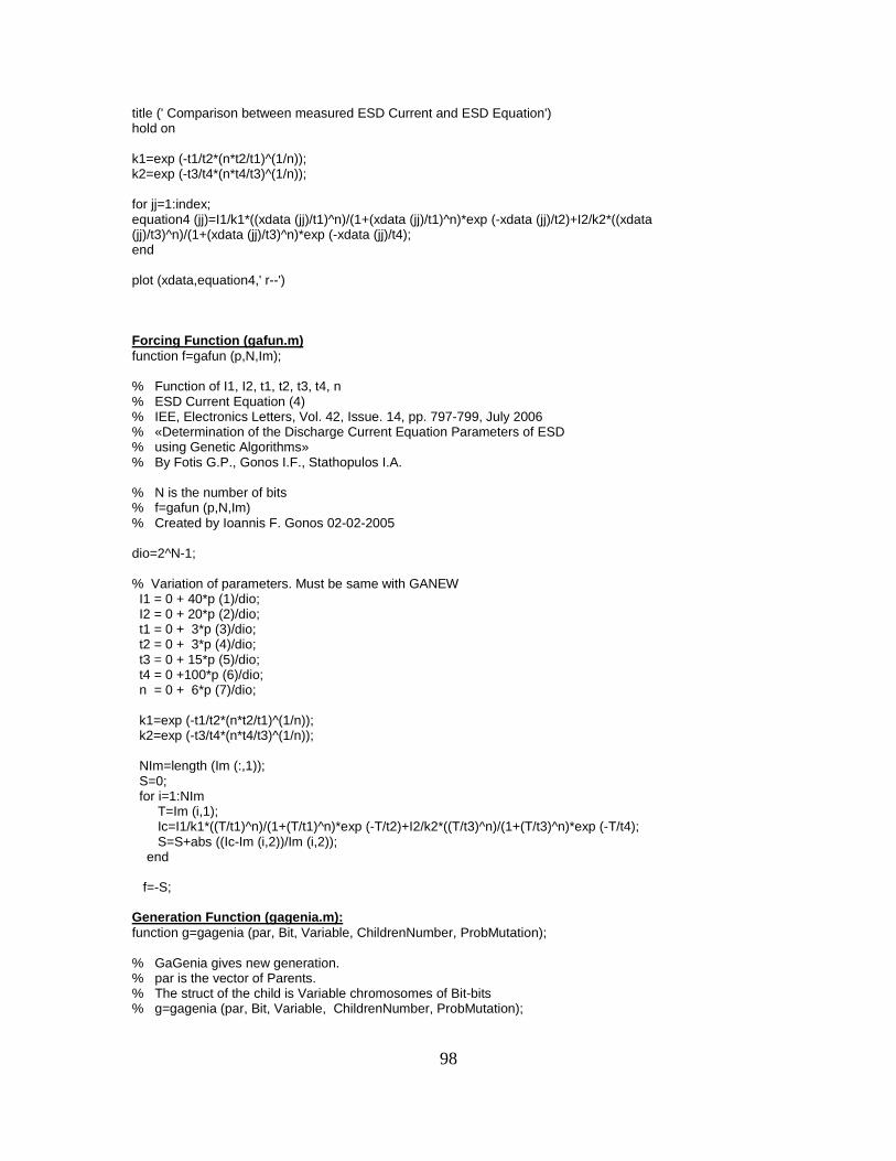
98
title (' Comparison between measured ESD Current and ESD Equation') hold on k1=exp (-t1/t2*(n*t2/t1)^(1/n)); k2=exp (-t3/t4*(n*t4/t3)^(1/n)); for jj=1:index; equation4 (jj)=I1/k1*((xdata (jj)/t1)^n)/(1+(xdata (jj)/t1)^n)*exp (-xdata (jj)/t2)+I2/k2*((xdata (jj)/t3)^n)/(1+(xdata (jj)/t3)^n)*exp (-xdata (jj)/t4); end plot (xdata,equation4,' r--') Forcing Function (gafun.m) function f=gafun (p,N,Im); % Function of I1, I2, t1, t2, t3, t4, n % ESD Current Equation (4) % IEE, Electronics Letters, Vol. 42, Issue. 14, pp. 797-799, July 2006 % «Determination of the Discharge Current Equation Parameters of ESD % using Genetic Algorithms» % By Fotis G.P., Gonos I.F., Stathopulos I.A. % N is the number of bits % f=gafun (p,N,Im) % Created by Ioannis F. Gonos 02-02-2005 dio=2^N-1; % Variation of parameters. Must be same with GANEW I1 = 0 + 40*p (1)/dio; I2 = 0 + 20*p (2)/dio; t1 = 0 + 3*p (3)/dio; t2 = 0 + 3*p (4)/dio; t3 = 0 + 15*p (5)/dio; t4 = 0 +100*p (6)/dio; n = 0 + 6*p (7)/dio; k1=exp (-t1/t2*(n*t2/t1)^(1/n)); k2=exp (-t3/t4*(n*t4/t3)^(1/n)); NIm=length (Im (:,1)); S=0; for i=1:NIm T=Im (i,1); Ic=I1/k1*((T/t1)^n)/(1+(T/t1)^n)*exp (-T/t2)+I2/k2*((T/t3)^n)/(1+(T/t3)^n)*exp (-T/t4); S=S+abs ((Ic-Im (i,2))/Im (i,2)); end f=-S; Generation Function (gagenia.m): function g=gagenia (par, Bit, Variable, ChildrenNumber, ProbMutation); % GaGenia gives new generation. % par is the vector of Parents. % The struct of the child is Variable chromosomes of Bit-bits % g=gagenia (par, Bit, Variable, ChildrenNumber, ProbMutation);

99
% Created by Ioannis F. Gonos 15-02-2000 PlithosGonion=size (par,1); goneis=ones (1, PlithosGonion); while sum (goneis)>0 % Selection of the first parents FirstGonios=floor (PlithosGonion*rand)+1; while goneis (FirstGonios) == 0, FirstGonios=FirstGonios+1; if FirstGonios>PlithosGonion FirstGonios=1; end; end if goneis (FirstGonios) == 1 goneis (FirstGonios) = 0; end % Selection of the second parents SecondGonios=floor (PlithosGonion*rand)+1; while goneis (SecondGonios) == 0, SecondGonios = SecondGonios+1; if SecondGonios>PlithosGonion SecondGonios=1; end end if goneis (SecondGonios) == 1 goneis (SecondGonios) = 0; end % Convertion of the Decimal data to binary data for i=1:Variable par1 (i,:)=ga10to2 (par (FirstGonios,i),Bit); par2 (i,:)=ga10to2 (par (SecondGonios,i),Bit); end % Birth of a child by crossover for c=1: ChildrenNumber child=crosover (par1,par2,Bit,Variable); if rand < ProbMutation child=mutation (child, Bit, Variable); end; children ((2*sum (goneis))+c,:)=GA2to10 (child,Bit,Variable); end end g=newgen (par,children, PlithosGonion, Bit, Variable); First Parents Generation (parents.m): function p=parents (NoP,N,M); % Parents gives the first generation. % NoP is the Number of Parents. % The struct of the child is M chromosome of N-bits % p=parents (NoP,N,M) % Created by Ioannis F. Gonos 15-02-2000 Megisto=2^N; for i=1:NoP for j=1:M p (i,j)=floor (Megisto*rand); end end New Parents Generation (newgen.m): function G=newgen (OldGen,Children, NoP,N,M); % The new generation of parents. % NoP is the Number of Parents. % The struct of the child is M chromosome of N-bits

100
% G=parents (NoP,N,M) % Created by Ioannis F. Gonos 15-02-2000 load B12kvPost.txt; Gen=OldGen; for i=1:size (Children,1) Gen (NoP+i,:)=Children (i,:); end change=0; while change==0 change=1; for i=1:(size (Gen,1)-1) if gafun (Gen (i,:),N,B12kvPost)<gafun (Gen (i+1,:),N,B12kvPost) Help=Gen (i,:); Gen (i,:)=Gen (i+1,:); Gen (i+1,:)=Help; change=0; end end end for i=1:NoP G (i,:)=Gen (i,:); end Mutation Function (mutation.m): function p=mutation (p,N,M); % Mutation converts a bit from a child. % The struct of the child is M chromosome of N-bits % p=mutation (p,N,M) % Created by Ioannis F. Gonos 15-02-2000 PositionY=1+floor (N*rand); PositionX=1+floor (M*rand); if p (PositionX, PositionY)==1 p (PositionX, PositionY)=0; else p (PositionX, PositionY)=1; end Crossover Function (crossover.m): function c=crosover (p1,p2,N,M); % Crossover born a child from two parents. % The struct of the parents is M chromosome N-bits % c=crosover (p1,p2,N,M) % Created by Ioannis F. Gonos 15-02-2000 for i=1:M CutPosition=1+floor ((N-1)*rand); for j=1:CutPosition c (i,j)=p1 (i,j); end for j=CutPosition+1:N c (i,j)=p2 (i,j); end end

101
Binary to Decimal Conversion (ga2to10.m): function d=ga2to10 (b,N,M); % GA2to10 Convert a binary array todecimal integer with at least N bits. % GA2to10 (B,N,M) produces the decimal representation of M N-bits binary % N bits. % Example % GA2to10 (0 1 0 1 1 1, 6, 1) returns 23 % Created by Ioannis F. Gonos 15-02-2000 d=zeros (1,M); two=1; for i=1:N for k=1:M d (k)=d (k)+(b (k,(N-i+1)))*two; end two=2*two; end Decimal to Binary Conversion (ga10to2.m): function b=ga10to2 (d,n) % GA10to2 Convert decimal integer to a binary array. % GA10to2 (D,N) produces a binary representation with at least % N bits. % Example % GA10to2 (23,6) returns 0 1 0 1 1 1 % Created by Ioannis F. Gonos 15-02-2000 for i=1:n b (n-i+1)=rem (d,2); d=floor (d/2); end
102
Bibliography
[1] Canada, G. o., “Space weather effects on satellites,” December 18, 2008, http://www.spaceweather.gc.ca/satellites_e.php.
[2] B. T. Harder, “Evaluation of Nanocomposites as Lightweight Electronic Enclosures for Satellites' Applications,” M.S. Thesis, Air Force Institute of Technology, Wright-Patterson AFB, 2008.
[3] C. K. Purvis and H.B. Garret, “Design guidelines for assessing and controlling spacecraft charging effects,” NASA Test Practice, TP-2361, 2004.
[4] J. Catani, J. and D. Payan, “Electrostatic Behavior of Materials in a Charging Space Environment, in 2004 International Conference on Solid Dielectrics, 5-9 July, 2004, Toulouse, France.
[5] G. L. Wrenn and R. J. Smith, “Probability Factors Governing ESD Effects in Geosynchronous Orbit,” IEEE Transactions on Nuclear Science, vol. 43, pg 2783, December 1996.
[6] Aerospace Corporation, “Center for Orbital and Reentry Debris Studies,” Space Operations Digest, vol. 1, Nov 2000.
[7] Metal Matrix Composites Copr LLC, “Nanostrands: ‘Nickel at Its Finest’,” 2004, http://www.nanostrands.com.
[8] M. Suzuki, Y. Ominami, and Q. Ngo, “Current-induced breakdown of carbon nanofibers,” Journal of Applied Physics, vol. 101, pp. 1143-47, November 2007.
[9] D. N. Baker, S. G. Kanekal and J. B. Blake, “Characterizing the Earth’s outer van allen zone using a radiation belt content index,” Space Weather, vol 2, pg. 1, 2004.
[10] Grossman, E., & Gouzman, I. (2003). Space environment effects on polymers in low earth orbit. Nuclear Instruments and Methods in Physics Research Section B: Beam Interactions with Materials and Atoms, 208, 48-57.
[11] J. F. Fennel and J. L. Koons, “Spacecraft Charging: Observations and Relationship to Satellite Anomalies,” The Aerospace Corporation, Los Angeles, CA, August 19, 2008, http://dev.spis.org/projects/spine/home/tools/sctc/VIIth/792b52ddc0a8001401d6d5b2dcb07057?action=download&nodecorator.
[12] “MAJ Thomas Quigley (USAF) Lecture Series,” provided as supplemental reading for PHY 519, “The Space Environment,” Department of Engineering Physics, Air Force Institute of Technology, Spring 2008.

103
[13] “The Magnetosphere,” class notes for PHY 519, “The Space Environment,” Department of Engineering Physics, Air Force Institute of Technology, Spring 2008.
[14] MIL-STD 1809, United States Air Force, “Space Environment for USAF Space Vehicles,” February 15, 1991.
[15] MIL-STD-1541(A), United States Air Force, “Electromagnetic Compatibility Requirements for Space Systems,” December 30, 1987.
[16] NASA, Jet Propulsion Laboratory, (2007). “Electrostatic Discharge (ESD) Test Practices,” Pasadena, California, PT-TE-1414, 2007.
[17] NASA, Scientific and Technical Information Branch, “Design Guidelines for Assessing and Controlling Spacecraft Charging Effects,” National Aeronautics and Space Administration, Houston, Texas, NASA-TP-2361, 1984. [18] French Aerospace Lab, ONERA. “Space Environment,” April 25, 2003, http://www.onera.fr/desp-en/technical-resources/sirene.php [19] E. Grossman and I. Gouzman, “Space environment effects on polymers in low earth orbit,” Nuclear Instruments and Methods in Physics Research Section B: Beam Interactions with Materials and Atoms, vol. 208, pp. 48-57, 2003.
[20] A. Holmes-Seidle and L. Adams, “Handbook of Radiation Effects,” London: Oxford University Press, 1993.
[21] A Yamanaka, Y. Izumi and T. Kitagawa, “The radiation effect on thermal conductivity of high strength ultra-high-molecular-weight polyethylene fiber by gamma-rays,” Journal of Applied Polymer Science, vol. 101(4), pp. 2619-2626, 2006.
[22] M. Beck, MURI Review, Vanderbilt University, “Elemental Defect Processes in Radiation-Induced Displacement Damage in Si,” June 13, 2006, http://www.isde.vanderbilt.edu/content/muri_2006/FINALbeck_MURIrev_June06.ppt.
[23] G. Hansen, “High aspect ratio sub-micron and nano-scale metal filaments,” SAMPE Journal, vol. 41(2), pp. 1-11, 2005.
[24] D. W. Clegg and A. J. Collyer, “Radiation Effects on Polymers,” Applied Science, London: Elsevier, 1991.
[25] MISSE: Material International Space Station Experiment. January 2007, http://misse3.larc.nasa.gov/
[26] G. Hansen, Metal Matrix Composites (private communication), telephonic, 20 August 2008.

104
[27] P. Kodali, Engineering Electromagnetic Compatibility. New York: IEEE Press, 2001.
[28] D Kind and K. Feser, High Voltage Test Techniques. New Delhi: Newnes, 2001.
[29] G. Cerri, R. Leo, and V. M. Primiani, “ESD indirect coupling modeling,” IEEE Transactions on Engineering Electromagnetic Compatibility, vol. 38, pp. 374-81, 1996.
[30] H. Heidler, “Analytische Blitzstromfunktion zur LEMP-Berechnung,” in 18th International Conference and Symposium on Logic Programming, 1985, pp. 63-6.
[31] K. Wang, D. Pommerenke, R. Chundru, T. M. Doren, J. L. Drewniak and A. Shashindranath, “Numerical modeling of electrostatic discharge generators,” IEEE Transactions on Engineering Electromagnetic Compatibility, vol. 45, pp. 258-70, 2003.
[32] S. V. Berghe and D. Zutter, “Study of ESD signal entry through coaxial cable shields,” Journal of Electrostatics, vol. 4, pp. 135-48, 1998.
[33] National Institute of Standards and Technology, Physics Laboratory, “Stopping-power and range tables for electrons (ESTAR) database,” November 2008, http://physics.nist.gov/phyrefdata/star/text/estar.html.
[34] G. F. Knoll, Radiation Detection and Measurement. New York: John Wiley & Sons, 2000.
[35] G. P. Fotis, F. E. Asimakopoulou, I. F. Gonos and I. A. Stathopulos, “Applying genetic algorithms for the determination of the parameters of the electrostatic discharge current equation,” Measurement Science and Technology, vol. 17, pp. 2819-27, 2006.
[36] I. F. Gonos, National Technical University, Athens, Greece, “Curriculum Vitae,” November 2008, http://users.ntua.gr/igonos/JFGEng.htm.
[37] C. A. Balanis, Advanced Engineering Electromagnetics. New York: John Wiley & Sons, 1989.
[38] Compliance Engineering, Niels Jonassen, DSc, “How Fast Does Charge Decay?” April 2006, http://ce-mag.htm.
[39] “Conduction Currents,” class notes for NENG 625, “Electromagnetic Pulse Effects,” Department of Engineering Physics, Air Force Institute of Technology, Summer 2008.
[40] J. C. Ritter, “Space Systems and Survivability a Historical Overview and Technical Background,” IEEE, Nuclear and Radiation Effects Conference Short Course, Marco Island, FL, 24 July 1989.

105
[41] Conversation with Max Alexander, AFRL/RXBN, 23 Jan 2009.
[42] D. Fink, Fundamentals of Ion-Irradiated Polymers. Springer, 2004, pp. 268.

106
REPORT DOCUMENTATION PAGE Form Approved OMB No. 074-0188
The public reporting burden for this collection of information is estimated to average 1 hour per response, including the time for reviewing instructions, searching existing data sources, gathering and maintaining the data needed, and completing and reviewing the collection of information. Send comments regarding this burden estimate or any other aspect of the collection of information, including suggestions for reducing this burden to Department of Defense, Washington Headquarters Services, Directorate for Information Operations and Reports (0704-0188), 1215 Jefferson Davis Highway, Suite 1204, Arlington, VA 22202-4302. Respondents should be aware that notwithstanding any other provision of law, no person shall be subject to an penalty for failing to comply with a collection of information if it does not display a currently valid OMB control number. PLEASE DO NOT RETURN YOUR FORM TO THE ABOVE ADDRESS. 1. REPORT DATE (DD-MM-YYYY) 27-03-2009
2. REPORT TYPE Master’s Thesis
3. DATES COVERED (From – To) June 2007-March 2009
4. TITLE AND SUBTITLE Electrostatic Discharge Properties of Irradiated Nanocomposites
5a. CONTRACT NUMBER
5b. GRANT NUMBER 5c. PROGRAM ELEMENT NUMBER
6. AUTHOR(S) Joshua D. McGary, Major, USA
5d. PROJECT NUMBER 5e. TASK NUMBER
5f. WORK UNIT NUMBER
7. PERFORMING ORGANIZATION NAMES(S) AND ADDRESS(S) Air Force Institute of Technology Graduate School of Engineering and Management (AFIT/EN) 2950 Hobson Way WPAFB OH 45433-7765
8. PERFORMING ORGANIZATION REPORT NUMBER AFIT/GNE/ENP/09-M03
9. SPONSORING/MONITORING AGENCY NAME(S) AND ADDRESS(ES) Intentionally Left Blank
10. SPONSOR/MONITOR’S ACRONYM(S) 11. SPONSOR/MONITOR’S REPORT NUMBER(S)
12. DISTRIBUTION/AVAILABILITY STATEMENT APPROVED FOR PUBLIC RELEASE; DISTRIBUTION UNLIMITED 13. SUPPLEMENTARY NOTES 14. ABSTRACT Modernization in space systems requires employment of new light-weight, high performance composite materials that reduce bulk weight and increase structural integrity. This thesis explored the behavior of one such material prior to and following a 35-year simulated space radiation life-cycle. Select electrical properties of nickel nanostrandTM-carbon composites in seven configurations were characterized prior to electron irradiation via surface and bulk resistivity measurements and contact electrostatic discharge (ESD) measurements. Following irradiation at a fluence of 1016 e-/cm2 at an average energy of 500 keV, measurements were repeated and compared against pre-irradiation data. Configuration D is the best configuration tested for use as a satellite external surface material. All composite configurations tested in this research showed degradation in critical electrical properties when examined in the aggregate. The data showed no common trend between the electrical performance of the various composites based on location or density of the nickel nanostrands™ in the material. Surface resistivity increased for all configurations while bulk resistivity change correlated to the type of epoxy resin used in the composite. The mechanism responsible for these changes is electron induced displacement damage within both the epoxy and carbon which reduce permittivity and, or conductivity within the bulk. ESD current waveform properties of peak current and decay time decreased in a manner sufficient to conclude that every configuration tested is subject to increased ESD frequency and intensity over a lifetime of space radiation. These materials require further engineering to better resist the changes noted in these electrical properties before used as satellite surfaces. 15. SUBJECT TERMS Nickel NanostrandsTM, Composites, Satellite Surfaces, Surface Resistivity, Bulk Resistivity, Electrostatic Discharge, Genetic Algorithm, Polarization, Permittivity, Conductivity, Electron Mobility, Scissioning 16. SECURITY CLASSIFICATION OF:
17. LIMITATION OF ABSTRACT UU
18. NUMBER OF PAGES 121
19a. NAME OF RESPONSIBLE PERSON James C. Petrosky, Ph.D.
REPORT U
ABSTRACT U
c. THIS PAGE U
19b. TELEPHONE NUMBER (Include area code) (937) 255-3636, ext 4562; e-mail: [email protected]
Standard Form 298 (Rev: 898) Prescribed by ANSI Std. Z39-18