Embed Size (px)
DESCRIPTION
paper
Citation preview
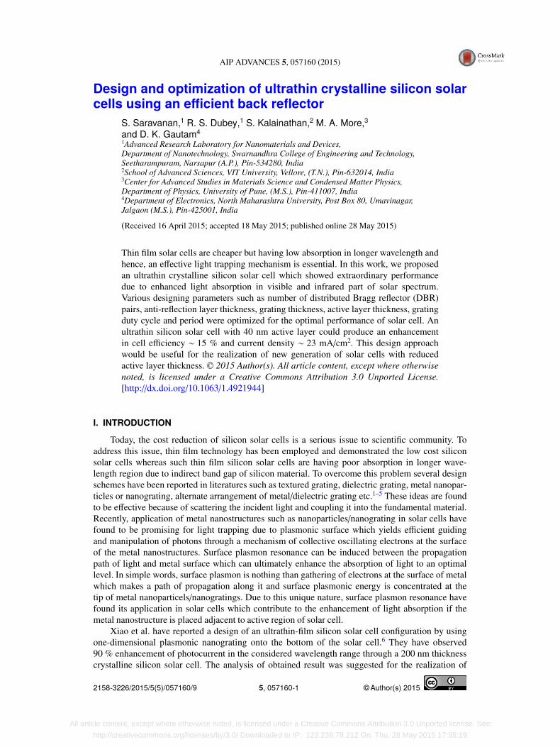
Design and optimization of ultrathin crystalline silicon solar cells using an efficientback reflectorS. Saravanan, R. S. Dubey, S. Kalainathan, M. A. More, and D. K. Gautam Citation: AIP Advances 5, 057160 (2015); doi: 10.1063/1.4921944 View online: http://dx.doi.org/10.1063/1.4921944 View Table of Contents: http://scitation.aip.org/content/aip/journal/adva/5/5?ver=pdfcov Published by the AIP Publishing Articles you may be interested in Multi-resonant silver nano-disk patterned thin film hydrogenated amorphous silicon solar cells for Staebler-Wronski effect compensation J. Appl. Phys. 116, 093103 (2014); 10.1063/1.4895099 Optimal design of one-dimensional photonic crystal back reflectors for thin-film silicon solar cells J. Appl. Phys. 116, 064508 (2014); 10.1063/1.4893180 Photonic assisted light trapping integrated in ultrathin crystalline silicon solar cells by nanoimprint lithography Appl. Phys. Lett. 101, 103901 (2012); 10.1063/1.4749810 Application of amorphous carbon based materials as antireflective coatings on crystalline silicon solar cells J. Appl. Phys. 110, 043510 (2011); 10.1063/1.3622515 Demonstration of enhanced absorption in thin film Si solar cells with textured photonic crystal back reflector Appl. Phys. Lett. 93, 221105 (2008); 10.1063/1.3039787
All article content, except where otherwise noted, is licensed under a Creative Commons Attribution 3.0 Unported license. See:
http://creativecommons.org/licenses/by/3.0/ Downloaded to IP: 123.239.78.212 On: Thu, 28 May 2015 17:35:19
AIP ADVANCES 5, 057160 (2015)
Design and optimization of ultrathin crystalline silicon solarcells using an efficient back reflector
S. Saravanan,1 R. S. Dubey,1 S. Kalainathan,2 M. A. More,3and D. K. Gautam41Advanced Research Laboratory for Nanomaterials and Devices,Department of Nanotechnology, Swarnandhra College of Engineering and Technology,Seetharampuram, Narsapur (A.P.), Pin-534280, India2School of Advanced Sciences, VIT University, Vellore, (T.N.), Pin-632014, India3Center for Advanced Studies in Materials Science and Condensed Matter Physics,Department of Physics, University of Pune, (M.S.), Pin-411007, India4Department of Electronics, North Maharashtra University, Post Box 80, Umavinagar,Jalgaon (M.S.), Pin-425001, India
(Received 16 April 2015; accepted 18 May 2015; published online 28 May 2015)
Thin film solar cells are cheaper but having low absorption in longer wavelength andhence, an effective light trapping mechanism is essential. In this work, we proposedan ultrathin crystalline silicon solar cell which showed extraordinary performancedue to enhanced light absorption in visible and infrared part of solar spectrum.Various designing parameters such as number of distributed Bragg reflector (DBR)pairs, anti-reflection layer thickness, grating thickness, active layer thickness, gratingduty cycle and period were optimized for the optimal performance of solar cell. Anultrathin silicon solar cell with 40 nm active layer could produce an enhancementin cell efficiency ∼ 15 % and current density ∼ 23 mA/cm2. This design approachwould be useful for the realization of new generation of solar cells with reducedactive layer thickness. C 2015 Author(s). All article content, except where otherwisenoted, is licensed under a Creative Commons Attribution 3.0 Unported License.[http://dx.doi.org/10.1063/1.4921944]
I. INTRODUCTION
Today, the cost reduction of silicon solar cells is a serious issue to scientific community. Toaddress this issue, thin film technology has been employed and demonstrated the low cost siliconsolar cells whereas such thin film silicon solar cells are having poor absorption in longer wave-length region due to indirect band gap of silicon material. To overcome this problem several designschemes have been reported in literatures such as textured grating, dielectric grating, metal nanopar-ticles or nanograting, alternate arrangement of metal/dielectric grating etc.1–5 These ideas are foundto be effective because of scattering the incident light and coupling it into the fundamental material.Recently, application of metal nanostructures such as nanoparticles/nanograting in solar cells havefound to be promising for light trapping due to plasmonic surface which yields efficient guidingand manipulation of photons through a mechanism of collective oscillating electrons at the surfaceof the metal nanostructures. Surface plasmon resonance can be induced between the propagationpath of light and metal surface which can ultimately enhance the absorption of light to an optimallevel. In simple words, surface plasmon is nothing than gathering of electrons at the surface of metalwhich makes a path of propagation along it and surface plasmonic energy is concentrated at thetip of metal nanoparticels/nanogratings. Due to this unique nature, surface plasmon resonance havefound its application in solar cells which contribute to the enhancement of light absorption if themetal nanostructure is placed adjacent to active region of solar cell.
Xiao et al. have reported a design of an ultrathin-film silicon solar cell configuration by usingone-dimensional plasmonic nanograting onto the bottom of the solar cell.6 They have observed90 % enhancement of photocurrent in the considered wavelength range through a 200 nm thicknesscrystalline silicon solar cell. The analysis of obtained result was suggested for the realization of
2158-3226/2015/5(5)/057160/9 5, 057160-1 ©Author(s) 2015
All article content, except where otherwise noted, is licensed under a Creative Commons Attribution 3.0 Unported license. See:
http://creativecommons.org/licenses/by/3.0/ Downloaded to IP: 123.239.78.212 On: Thu, 28 May 2015 17:35:19
057160-2 Saravanan et al. AIP Advances 5, 057160 (2015)
low cost and high efficiency thin film solar cells. He et al. have proposed a design of an ultrathinsilicon solar cell by placing a periodic array of silver strips on a metallic nanograting substrate.7 Thedesigned structure could give 170 % light absorption enhancement as comparison to the bare siliconthin film. This enhancement has been attributed to the excited multiple resonant and waveguidingmodes within the silicon layer, localized surface plasmon resonance and surface plasmon polaritons.Reduced cell thickness is a critical issue in silicon solar cells, when it is less than 2 µm (c-Si) andbelow 300 nm (a-Si:H). Therefore, ultrathin solar cells light trapping is essential whereas plasmonicsolar cells are found to be more promising to overcome this problem. Yan et al. have presented athree modeling methods for a-Si:H solar cells and to observe the light absorption, parabolaconicalnanoarrays were introduced into ultrathin a-Si:H solar cells.8 They observed optimal absorptionenhancement (53.9 %) when height/radius ratio was 1 and further, it was increased to 61.9 % forthe case when height/radius ratio was 3. This enhancement was due to the graded refractive indexof silicon and waveguide mode. Wang et al. have proposed a planar ultrathin absorber concept byexploiting plasmonic resonance absorption enhancement and obtained enhanced absorption about89.8 % through 5 nm thin film absorber which showed single pass absorption of only 1.7% forthe case of TM polarization.9 The absorption enhancement was broadband and angle-independent.Furthermore, this concept was suggested for 2D periodic grating geometries to achieve a strongangle and polarization independent absorption analysis. Juan et al. have reported a design of solarcell with the influence of relative position of silver metallic nanoparticles which was embeddedin a 100 nm anti-reflection coating layer.10 It was demonstrated that this plasmonic anti-reflectioncoating layer could achieve lower reflections as comparison to that SiOx anti-reflection coatinglayer but addition of silver nanoparticles in front surface geometry have generated poor interfer-ences due to which the efficiency of cell was found to be reduced. Sheng et al. have analyticallyinvestigated the light trapping mechanism in plasmonic silicon solar cells.11 This designing wasexplored by considering absorption enhancement for surface plasmon polaritons (SPPs) at planarsilicon-metal interfaces and localized surface plasmon resonances (LSPRs) for metallic spheres ina silicon matrix. They observed that the absorption enhancement factor was not bound to Lamber-tian limit and localized plasmonic resonances can be used as efficient light trapping schemes forultrathin silicon solar cells. Chriki et al. have proposed an ultrathin solar cell design by incorpo-rating two periodic layers of metallic and dielectric gratings.12 Both layers could able to couplethe incident light to photonic and plasmonic modes and hence, enhanced absorption of light wasachieved. A relative position between the two gratings was analyzed and observed a significanteffect. The proposed design was compared with a reference solar cell of a single layer of metallicand dielectric nanostructures respectively and found to be satisfactory in term of high absorption fordual grating design. Plasmonic solar cells are promising to produce high efficiency due to its highcarrier collection and less bulk recombination. Spinelli et al. have presented two possible ways ofintegrating metal nanoparticles in a solar cell: first one is a coating of silver nanoparticles which isacts as antireflective surface and second one is application of regular and random arrays of metalnanostructures which couple light in waveguide modes.13 By employing a relative inexpensivenano-imprint technique, design of solar cell was attempted which showed an improvement in cellefficiency. In plasmonic solar cells, photons are trapped into localized surface plasmon (LSP) asa result it induces the surface plasmon (SP) which propagates transversely into active layer. Chaoet al. have proposed a plasmonic multilayer structure (PMS) for the application in ultrathin solarcell with 30 nm thick amorphous silicon (α-Si) as active layer. With the use of plasmonic multilayerstructure, they have observed a large absorbed photon number (∼ 28.7 %) as compare to the indiumtin oxide (ITO)/α-Si/Ag structure for the normal incident case of transverse magnetic (TM) polari-zation.14 Lee et al. have numerically presented the design of amorphous silicon (a-Si) thin film solarcell by employing ultrathin top into a-Si active layer. They have observed enhanced absorption witha wide range of incident angle for TM polarization through the solar cell with 30 nm thickness. Theoverall absorption for TM polarization was improved about 25 % as comparison to a solar cell withthicker metal grating however, for TE polarization 2.5 times improvement was observed.15
In this work, we propose a novel design of ultrathin silicon solar cells with an efficient lighttrapping structure comprising of top anti-reflection coating (ARC) of silicon nitride and bottomreflector composed of aluminum (Al) grating and a distributed Bragg reflector (DBR) made of
All article content, except where otherwise noted, is licensed under a Creative Commons Attribution 3.0 Unported license. See:
http://creativecommons.org/licenses/by/3.0/ Downloaded to IP: 123.239.78.212 On: Thu, 28 May 2015 17:35:19
057160-3 Saravanan et al. AIP Advances 5, 057160 (2015)
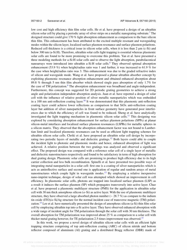
FIG. 1. Schematic diagram of ultrathin silicon solar cell (fig.a) and field distribution in the device for TE and TMpolarizations (fig.b).
a-Si/SiO2 materials. The optimized solar cell design could produce enhanced cell efficiency dueto broad band absorption in visible and infrared part of solar spectrum. In section second, designapproach is presented and simulated results are discussed in section third. Finally, section fourthconcludes the paper.
II. DESIGN & SIMULATION APPROACH
A schematic design of crystalline silicon (c-Si) thin film solar cell with an ultrathin active layer(50 nm) is shown in figure 1. It is comprised of an ARC layer (Si3N4), a DBR structure (a-Si/SiO2)and metal grating structure (Al). The DBR pairs was composed of alternate layers of a-Si and SiO2
with their refractive index 3.6 and 1.45 and thicknesses 41(t1) and 103 nm (t2) respectively whereascenter wavelength of DBR was 600 nm. The assumed thicknesses of ARC layer (t5) and Al grating(t3) were 70 and 50 nm respectively. In this simulation, the refractive index of the active region‘nc=3.5’ and its thickness ‘t4=50 nm’ were used.
The aluminum (Al) gratings help to diffract the incident light at oblique angles whereas distrib-uted Bragg reflector (DBR) resists the metal diffusion and sustain the mechanism of light trapping.The back reflector with the combination of DBR and metal grating is supposed to be an efficientlight trapping structure which utilizes the longer wavelength light by enforcing those in activeregion of solar cell. Table I displays the initial parametrical values considered for the design ofultrathin solar cell.
TABLE I. Design parameters of ultrathin silicon solar cell.
Parameters Values
grating period (Gp) 600 nmgrating duty cycle (Gdc) 0.5grating thickness (t3) 50 nmgrating tooth width (Gw) 300 nmno. of DBR pairs 5anti-reflection coating thickness (t5) 70 nmDBR center wavelength (λc) 600 nmactive layer thickness (t4) 50 nmDBR first layer a-Si thickness (t1) 41 nmDBR second layer SiO2 thickness(t2) 103 nm
All article content, except where otherwise noted, is licensed under a Creative Commons Attribution 3.0 Unported license. See:
http://creativecommons.org/licenses/by/3.0/ Downloaded to IP: 123.239.78.212 On: Thu, 28 May 2015 17:35:19
057160-4 Saravanan et al. AIP Advances 5, 057160 (2015)
For simulation, commercial available finite difference time domain method (FDTD) tool sup-plied by Rsoft Design Group was used. The periodic boundary conditions were applied in xand y-directions whereas in z-direction, perfectly matched layer boundary condition was per-formed. The solar cell was illuminated by plane wave under normal incidence from wavelength400-1200 nm. Figure 1(b) depicts electric field profile of designed solar cell for TE (at 741 nm) andTM (at 839 nm) polarizations with defined parameters in table I. For the case of TE polarization,electric field is visible near the gratings however, localized field at the tip of metal gratings is visiblefor the case of TM polarization. This cell could give cell efficiency 10.5 % with the use of five pairsof DBR for s-polarization case. The optimization of solar cell design by considering ARC thickness,grating thickness, active layer thickness, duty cycle and grating period is presented in next section.As solar radiation is having both transverse electric (TE) and transverse magnetic (TM) wavestherefore, we have extended our study for both polarizations.
III. RESULTS & DISCUSSION
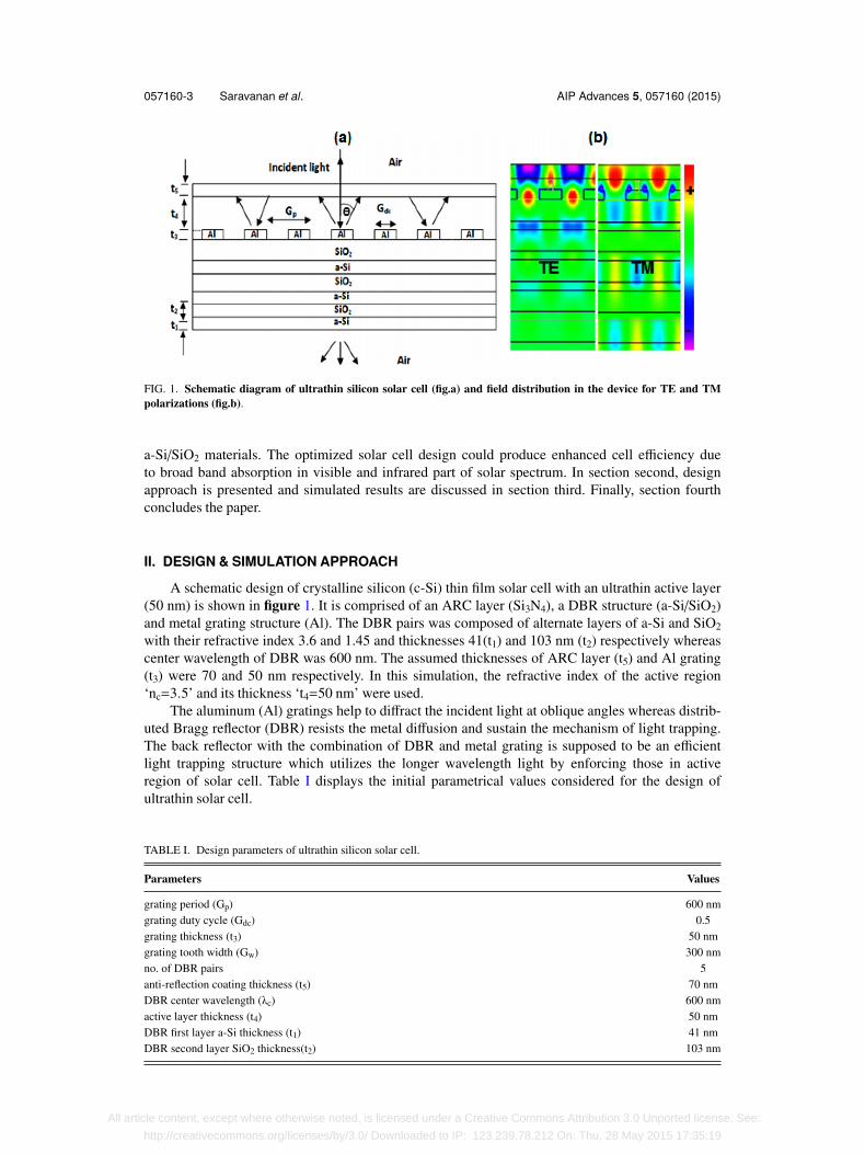
Initially, we have optimized the number of DBR pairs required for optimal performance ofproposed solar cell and found that three DBR pairs were satisfactory. Anti-reflection coating (ARC)layer plays a significant role to trap and pass light into the photovoltaic devices. Among other ARCmaterials, single layer of Si3N4 have been preferred for effective reduction of surface reflectionsof incident light. A solar cell with the parameters discussed in previous section was simulated forthe analysis of effect of ARC layer thickness. Figure 2 depicts the cell efficiency (solid line) inaccordance to ARC thickness. Reasonably, an enhancement in cell efficiency from 10.5 % to 11.6 %is observed at ARC layer thickness (t5) of 65 nm instead of 70 nm used previously. This result is asupplementary evidence of importance of ARC layer in term of its thickness which can be tuned tohave optimal transmission of solar light into silicon active region.
The diffraction grating as a part of the back reflector plays vital role in light trapping oflonger wavelength light. By replacing the optimized value of ARC layer thickness further, we have
FIG. 2. Solar cell efficiency as a function of ARC thickness (solid line) and grating thickness (dashed line).
All article content, except where otherwise noted, is licensed under a Creative Commons Attribution 3.0 Unported license. See:
http://creativecommons.org/licenses/by/3.0/ Downloaded to IP: 123.239.78.212 On: Thu, 28 May 2015 17:35:19
057160-5 Saravanan et al. AIP Advances 5, 057160 (2015)
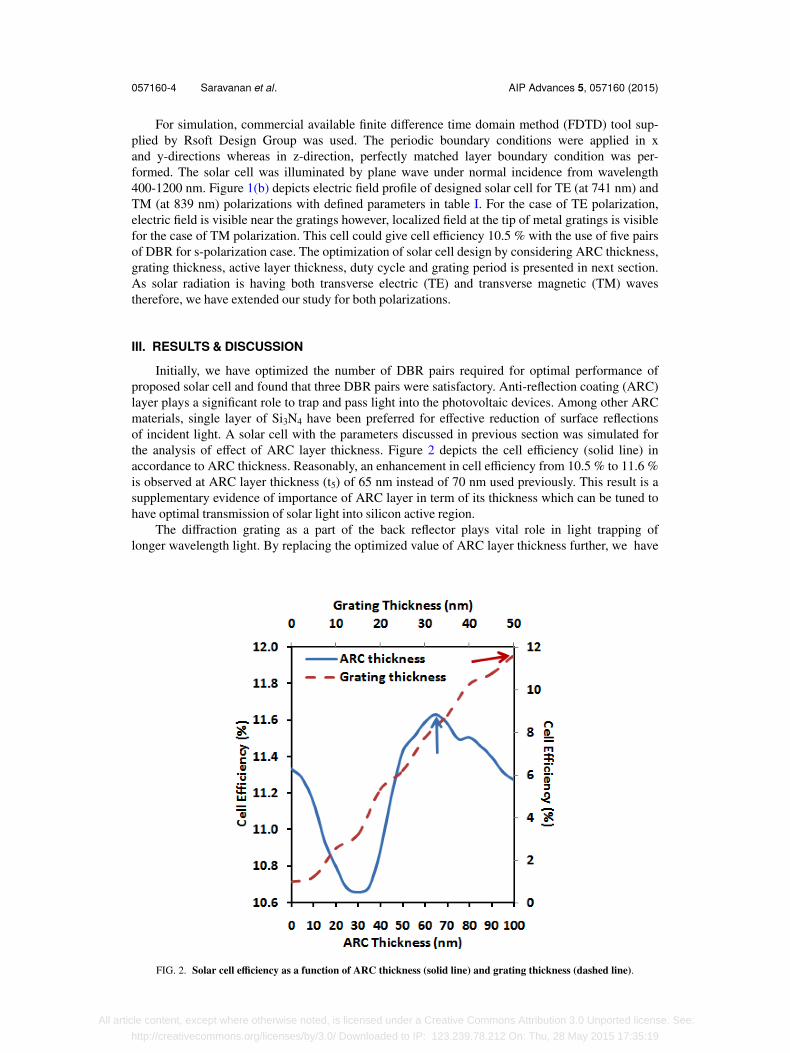
FIG. 3. Solar cell efficiency in accordance with active layer thickness.
optimized the thickness of aluminum grating. Figure 2 depicts the cell efficiency (dashed line) as afunction of grating thickness. As the grating thickness increased the conversion efficiency was alsofound to be increased, gradually. The usual behavior of grating thickness can be observed whereasmaximum efficiency 11.6 % (same as previous) was obtained at 50 nm. Our result shows that initialconsidered value of grating thickness was correct one. The obtained short-circuit current densitywas 17.67 mA/cm2.
We have explored our analysis for the effect of active layer thickness by keeping all parametersconstant except active layer thickness (t4). Figure 3 shows the variation of active layer thicknessagainst cell efficiency. An exponential enhancement in cell efficiency is observed and further than40 nm a decrease in cell efficiency is observed.
This reduction of cell efficiency indicates no longer use of back reflector due to increased cellthickness. This result is validated with reported work in which effective role of back reflector wasfound below 10 µm cell thickness and beyond it, the contribution of back reflector was rapidlydecreased.16 An enhancement in cell efficiency (12 %) is observed with cell thickness 40 nm whileshort-circuit current density was 18.28 mA/cm2. For further simulation, 50 nm cell thickness wasreplaced with an optimized one i.e. 40 nm.
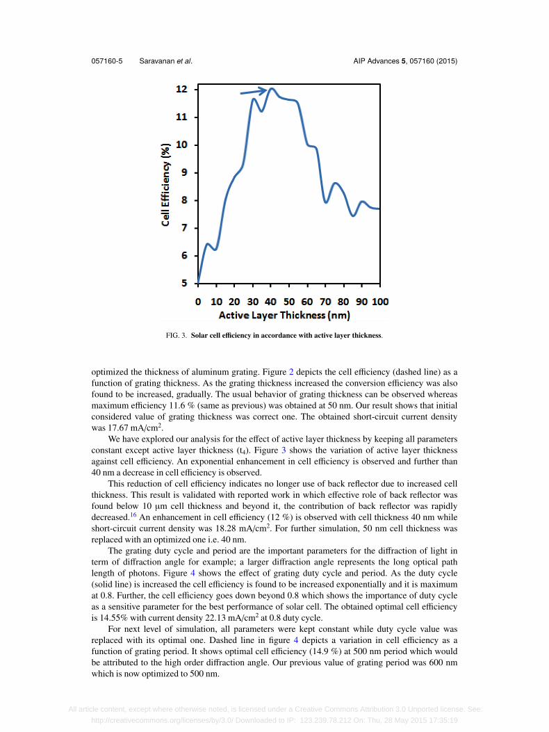
The grating duty cycle and period are the important parameters for the diffraction of light interm of diffraction angle for example; a larger diffraction angle represents the long optical pathlength of photons. Figure 4 shows the effect of grating duty cycle and period. As the duty cycle(solid line) is increased the cell efficiency is found to be increased exponentially and it is maximumat 0.8. Further, the cell efficiency goes down beyond 0.8 which shows the importance of duty cycleas a sensitive parameter for the best performance of solar cell. The obtained optimal cell efficiencyis 14.55% with current density 22.13 mA/cm2 at 0.8 duty cycle.
For next level of simulation, all parameters were kept constant while duty cycle value wasreplaced with its optimal one. Dashed line in figure 4 depicts a variation in cell efficiency as afunction of grating period. It shows optimal cell efficiency (14.9 %) at 500 nm period which wouldbe attributed to the high order diffraction angle. Our previous value of grating period was 600 nmwhich is now optimized to 500 nm.
All article content, except where otherwise noted, is licensed under a Creative Commons Attribution 3.0 Unported license. See:
http://creativecommons.org/licenses/by/3.0/ Downloaded to IP: 123.239.78.212 On: Thu, 28 May 2015 17:35:19

057160-6 Saravanan et al. AIP Advances 5, 057160 (2015)
FIG. 4. Solar cell efficiency in accordance with grating duty cycle (solid line) and grating period (dashed line).
Finally, with all optimized parameters we could able to obtain ∼15 % cell efficiency with40 nm cell thickness. To conclude the simulation results after above discussed optimization, wehave plotted the absorption curves in figure 5.
If we observe the absorption curve of grating thickness (t3), an enhanced absorption can beobserved in infrared wavelength region with a peak centered at 680 nm. The curves of grating thick-ness (t3) and ARC layer thickness (t5) are superimposed as the assumption of grating thickness value
FIG. 5. Light absorption behavior in silicon active layer of each optimization.
All article content, except where otherwise noted, is licensed under a Creative Commons Attribution 3.0 Unported license. See:
http://creativecommons.org/licenses/by/3.0/ Downloaded to IP: 123.239.78.212 On: Thu, 28 May 2015 17:35:19
057160-7 Saravanan et al. AIP Advances 5, 057160 (2015)
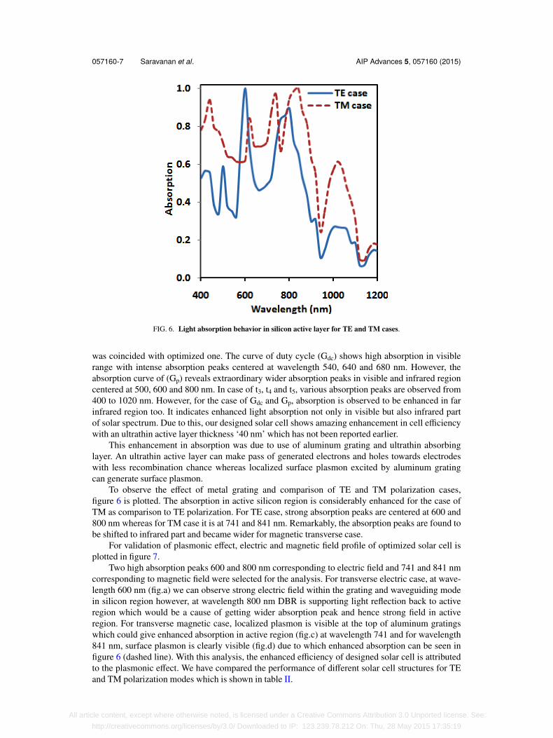
FIG. 6. Light absorption behavior in silicon active layer for TE and TM cases.
was coincided with optimized one. The curve of duty cycle (Gdc) shows high absorption in visiblerange with intense absorption peaks centered at wavelength 540, 640 and 680 nm. However, theabsorption curve of (Gp) reveals extraordinary wider absorption peaks in visible and infrared regioncentered at 500, 600 and 800 nm. In case of t3, t4 and t5, various absorption peaks are observed from400 to 1020 nm. However, for the case of Gdc and Gp, absorption is observed to be enhanced in farinfrared region too. It indicates enhanced light absorption not only in visible but also infrared partof solar spectrum. Due to this, our designed solar cell shows amazing enhancement in cell efficiencywith an ultrathin active layer thickness ‘40 nm’ which has not been reported earlier.
This enhancement in absorption was due to use of aluminum grating and ultrathin absorbinglayer. An ultrathin active layer can make pass of generated electrons and holes towards electrodeswith less recombination chance whereas localized surface plasmon excited by aluminum gratingcan generate surface plasmon.
To observe the effect of metal grating and comparison of TE and TM polarization cases,figure 6 is plotted. The absorption in active silicon region is considerably enhanced for the case ofTM as comparison to TE polarization. For TE case, strong absorption peaks are centered at 600 and800 nm whereas for TM case it is at 741 and 841 nm. Remarkably, the absorption peaks are found tobe shifted to infrared part and became wider for magnetic transverse case.
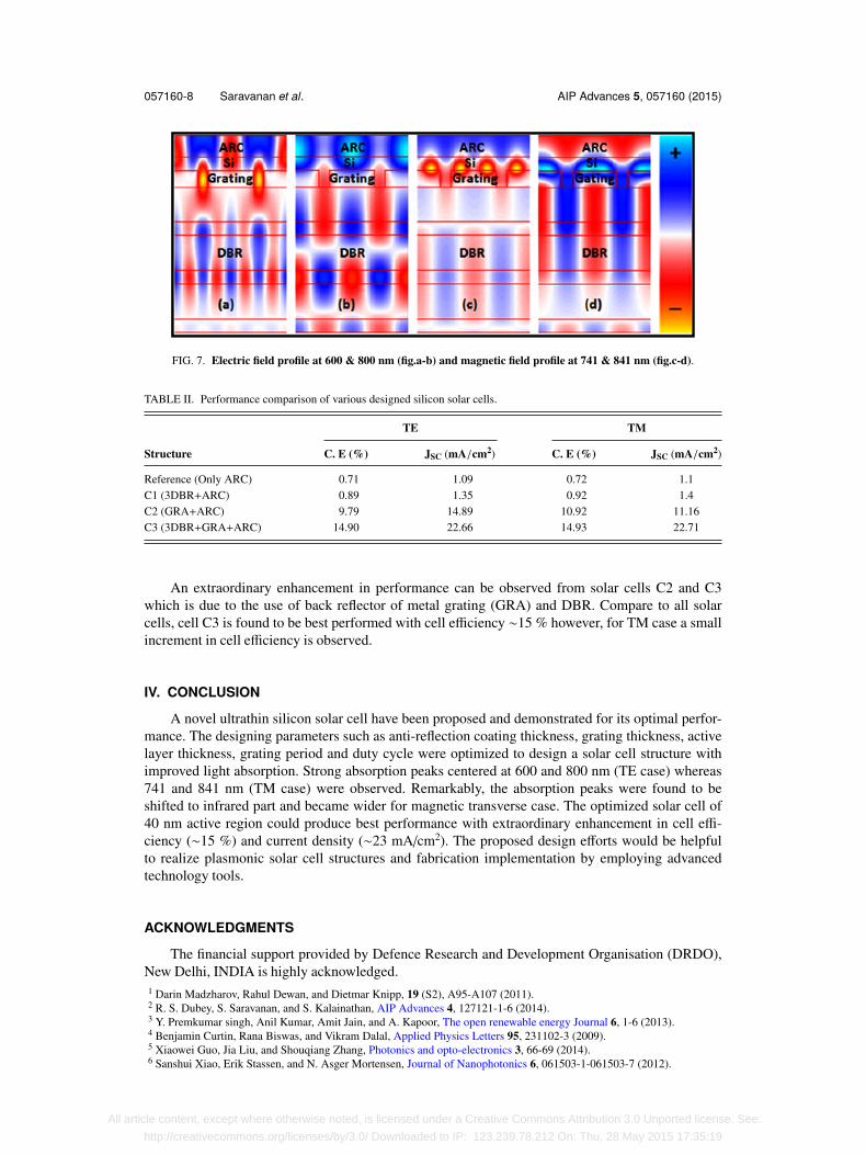
For validation of plasmonic effect, electric and magnetic field profile of optimized solar cell isplotted in figure 7.
Two high absorption peaks 600 and 800 nm corresponding to electric field and 741 and 841 nmcorresponding to magnetic field were selected for the analysis. For transverse electric case, at wave-length 600 nm (fig.a) we can observe strong electric field within the grating and waveguiding modein silicon region however, at wavelength 800 nm DBR is supporting light reflection back to activeregion which would be a cause of getting wider absorption peak and hence strong field in activeregion. For transverse magnetic case, localized plasmon is visible at the top of aluminum gratingswhich could give enhanced absorption in active region (fig.c) at wavelength 741 and for wavelength841 nm, surface plasmon is clearly visible (fig.d) due to which enhanced absorption can be seen infigure 6 (dashed line). With this analysis, the enhanced efficiency of designed solar cell is attributedto the plasmonic effect. We have compared the performance of different solar cell structures for TEand TM polarization modes which is shown in table II.
All article content, except where otherwise noted, is licensed under a Creative Commons Attribution 3.0 Unported license. See:
http://creativecommons.org/licenses/by/3.0/ Downloaded to IP: 123.239.78.212 On: Thu, 28 May 2015 17:35:19
057160-8 Saravanan et al. AIP Advances 5, 057160 (2015)
FIG. 7. Electric field profile at 600 & 800 nm (fig.a-b) and magnetic field profile at 741 & 841 nm (fig.c-d).
TABLE II. Performance comparison of various designed silicon solar cells.
TE TM
Structure C. E (%) JSC (mA/cm2) C. E (%) JSC (mA/cm2)
Reference (Only ARC) 0.71 1.09 0.72 1.1C1 (3DBR+ARC) 0.89 1.35 0.92 1.4C2 (GRA+ARC) 9.79 14.89 10.92 11.16C3 (3DBR+GRA+ARC) 14.90 22.66 14.93 22.71
An extraordinary enhancement in performance can be observed from solar cells C2 and C3which is due to the use of back reflector of metal grating (GRA) and DBR. Compare to all solarcells, cell C3 is found to be best performed with cell efficiency ∼15 % however, for TM case a smallincrement in cell efficiency is observed.
IV. CONCLUSION
A novel ultrathin silicon solar cell have been proposed and demonstrated for its optimal perfor-mance. The designing parameters such as anti-reflection coating thickness, grating thickness, activelayer thickness, grating period and duty cycle were optimized to design a solar cell structure withimproved light absorption. Strong absorption peaks centered at 600 and 800 nm (TE case) whereas741 and 841 nm (TM case) were observed. Remarkably, the absorption peaks were found to beshifted to infrared part and became wider for magnetic transverse case. The optimized solar cell of40 nm active region could produce best performance with extraordinary enhancement in cell effi-ciency (∼15 %) and current density (∼23 mA/cm2). The proposed design efforts would be helpfulto realize plasmonic solar cell structures and fabrication implementation by employing advancedtechnology tools.
ACKNOWLEDGMENTS
The financial support provided by Defence Research and Development Organisation (DRDO),New Delhi, INDIA is highly acknowledged.1 Darin Madzharov, Rahul Dewan, and Dietmar Knipp, 19 (S2), A95-A107 (2011).2 R. S. Dubey, S. Saravanan, and S. Kalainathan, AIP Advances 4, 127121-1-6 (2014).3 Y. Premkumar singh, Anil Kumar, Amit Jain, and A. Kapoor, The open renewable energy Journal 6, 1-6 (2013).4 Benjamin Curtin, Rana Biswas, and Vikram Dalal, Applied Physics Letters 95, 231102-3 (2009).5 Xiaowei Guo, Jia Liu, and Shouqiang Zhang, Photonics and opto-electronics 3, 66-69 (2014).6 Sanshui Xiao, Erik Stassen, and N. Asger Mortensen, Journal of Nanophotonics 6, 061503-1-061503-7 (2012).
All article content, except where otherwise noted, is licensed under a Creative Commons Attribution 3.0 Unported license. See:
http://creativecommons.org/licenses/by/3.0/ Downloaded to IP: 123.239.78.212 On: Thu, 28 May 2015 17:35:19

057160-9 Saravanan et al. AIP Advances 5, 057160 (2015)
7 Jinna He, Chunzhen Fan, Junqiao Wang, Yongguang Cheng, Pei Ding, and Erjun Liang1, Advances in OptoElectronics,Article ID 592754, doi:10.1155/2012/592754, 8 pages (2012).
8 Wensheng Yan and Min Gu, J. Opt. 16, 045003-6 (2014).9 Zhu Wang, Thomas P. White, and Kylie R. Catchpole, IEEE Photonics Journal 5(5), 8400608-8 (2013).
10 F. Cortes-Juan, C. Chaverri Ramos, J. P. Connolly, C. David, F. J. Garcıa de Abajo, J. Hurtado, V. D. Mihailetchi, S.Ponce-Alcantara, and Guillermo Sanchez, J. Renewable Sustainable Energy 5, 033116-12 (2013).
11 Xing Sheng, Juejun Hu, Jurgen Michel, and Lionel C. Kimerling, Optics Express 20(S4), A496-501 (2012).12 Ronen Chriki, Avner Yanai, Joseph Shappir, and Uriel Levy, Optics Express 21((S)3), A382-A391 (2013).13 P Spinelli, V E Ferry, J van de Groep, M van Lare, M A Verschuuren, R E I Schropp, H A Atwater, and A Polman, J. Opt.
14, 024002-11 (2012).14 Chien-Chang Chao, Chih-Ming Wang, Yia-Chung Chang, and Jenq-Yang Chang, Optical Review 16(3), 343-346 (2009).15 Sangjun Lee and Sangin Kim, IEEE Photonics Journal 5(5), 4800610-11 (2013).16 Ning-Ning Feng, J. Michel, Lirong Zeng, Jifeng Liu, Ching-Yin Hong, L. C. Kimerling, Duan, and Xiaoman, IEEE Trans-
actions on Electron Devices 54(8), 1926-1933 (2007).
All article content, except where otherwise noted, is licensed under a Creative Commons Attribution 3.0 Unported license. See:
http://creativecommons.org/licenses/by/3.0/ Downloaded to IP: 123.239.78.212 On: Thu, 28 May 2015 17:35:19


![Advances in Microbial Physiology [Vol 46] (Elsevier, 2002) WW](https://img.pdfslide.us/doc/110x75/613caa5d9cc893456e1e971c/advances-in-microbial-physiology-vol-46-elsevier-2002-ww.jpg)


![Advances in Cancer Research [Vol 99] (Elsevier, 2008) WW](https://img.pdfslide.us/doc/110x75/613caa549cc893456e1e96f6/advances-in-cancer-research-vol-99-elsevier-2008-ww.jpg)
![Advances in Immunology [Vol 102] (AP, 2009) WW](https://img.pdfslide.us/doc/110x75/613caa5c9cc893456e1e9716/advances-in-immunology-vol-102-ap-2009-ww.jpg)