Embed Size (px)
Citation preview
AIDA-SLIDE-2015-041
AIDAAdvanced European Infrastructures for Detectors at Accelerators
Presentation
Design of a FE ASIC in TSMC-65nm forSi tracking at the ILC
Casanova, R (UB)
22 October 2012
The research leading to these results has received funding from the European Commissionunder the FP7 Research Infrastructures project AIDA, grant agreement no. 262025.
This work is part of AIDA Work Package 9: Advanced infrastructures for detector R&D.
The electronic version of this AIDA Publication is available via the AIDA web site<http://cern.ch/aida> or on the CERN Document Server at the following URL:
<http://cds.cern.ch/search?p=AIDA-SLIDE-2015-041>
AIDA-SLIDE-2015-041
Dr. Raimon Casanova [email protected], University of Texas at Arlington(USA), 22-26 October 2012
Design of a FE ASIC in TSMC-65nm for Si tracking at the ILC
Angel Diéguez, Andreu Montiel, Raimon Casanova, Oscar Alonso
Departament d’Electrònica, Universitat de Barcelona
International Workshop on Future Linear Colliders 2012
Dr. Raimon Casanova [email protected], University of Texas at Arlington(USA), 22-26 October 2012
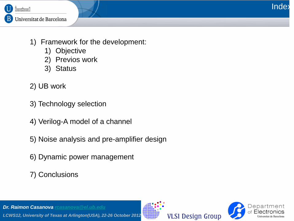
Index
1) Framework for the development:1) Objective2) Previos work3) Status
2) UB work
3) Technology selection
4) Verilog-A model of a channel
5) Noise analysis and pre-amplifier design
6) Dynamic power management
7) Conclusions
Dr. Raimon Casanova [email protected], University of Texas at Arlington(USA), 22-26 October 2012
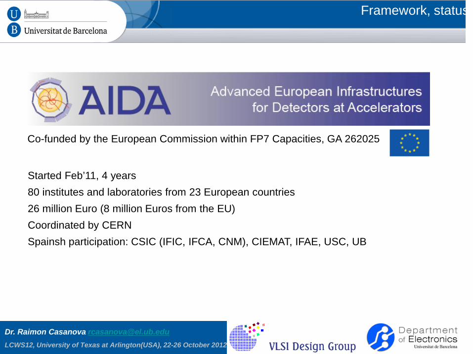
Started Feb’11, 4 years80 institutes and laboratories from 23 European countries26 million Euro (8 million Euros from the EU)Coordinated by CERNSpainsh participation: CSIC (IFIC, IFCA, CNM), CIEMAT, IFAE, USC, UB
Co-funded by the European Commission within FP7 Capacities, GA 262025
Framework, status
Dr. Raimon Casanova [email protected], University of Texas at Arlington(USA), 22-26 October 2012
WP9.4 Silicon TrackingCoordinated by Thomas Bergauer (HEPHY)Goal is the creation of a multi-layer micro-strip detector coverage for the calorimeter infrastructure (Task 9.5) to provide a precise entry point of charged particle
– The calorimeter infrastructure of task 9.5 will be preceded by several layers of Silicon micro-strip detectors to provide a precise entry point over a large area.
– Finely segmented and thin Silicon micro-strip detectors will be designed andprocured by the participating institutes.
– Baseline design system with readout with APV25. New readout chip designed by UB targetted for longer shaping time.
Co-funded by the European Commission within FP7 Capacities, GA 262025
Framework, status
Dr. Raimon Casanova [email protected], University of Texas at Arlington(USA), 22-26 October 2012
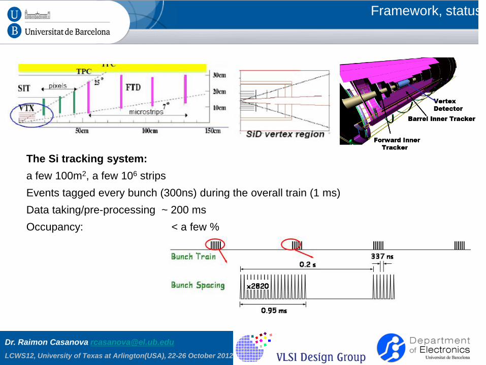
The Si tracking system: a few 100m2, a few 106 stripsEvents tagged every bunch (300ns) during the overall train (1 ms)Data taking/pre-processing ~ 200 msOccupancy: < a few %
Framework, status
Dr. Raimon Casanova [email protected], University of Texas at Arlington(USA), 22-26 October 2012
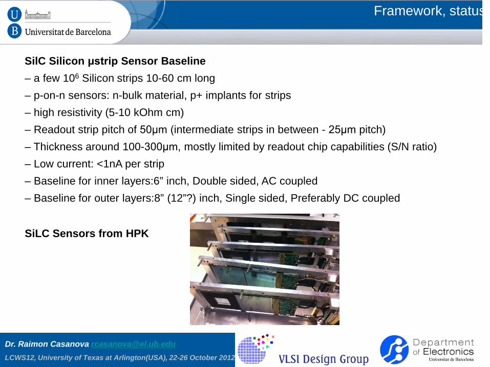
SilC Silicon μstrip Sensor Baseline– a few 106 Silicon strips 10-60 cm long– p-on-n sensors: n-bulk material, p+ implants for strips– high resistivity (5-10 kOhm cm)– Readout strip pitch of 50μm (intermediate strips in between - 25μm pitch)– Thickness around 100-300μm, mostly limited by readout chip capabilities (S/N ratio)– Low current: <1nA per strip– Baseline for inner layers:6” inch, Double sided, AC coupled– Baseline for outer layers:8” (12”?) inch, Single sided, Preferably DC coupled
SiLC Sensors from HPK
Framework, status
Dr. Raimon Casanova [email protected], University of Texas at Arlington(USA), 22-26 October 2012
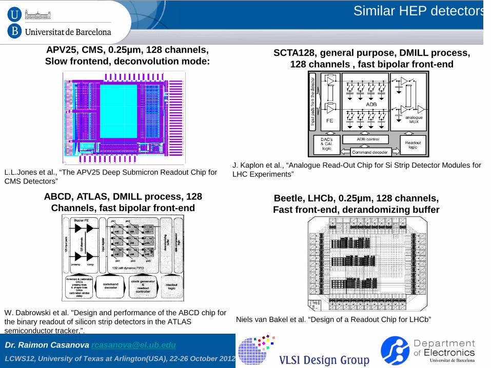
Similar HEP detectors
APV25, CMS, 0.25µm, 128 channels,Slow frontend, deconvolution mode:
ABCD, ATLAS, DMILL process, 128Channels, fast bipolar front-end
SCTA128, general purpose, DMILL process,128 channels , fast bipolar front-end
Beetle, LHCb, 0.25µm, 128 channels,Fast front-end, derandomizing buffer
W. Dabrowski et al. "Design and performance of the ABCD chip for the binary readout of silicon strip detectors in the ATLAS semiconductor tracker,”.
L.L.Jones et al., “The APV25 Deep Submicron Readout Chip for CMS Detectors”
Niels van Bakel et al. “Design of a Readout Chip for LHCb”
J. Kaplon et al., “Analogue Read-Out Chip for Si Strip Detector Modules for LHC Experiments”
Dr. Raimon Casanova [email protected], University of Texas at Arlington(USA), 22-26 October 2012
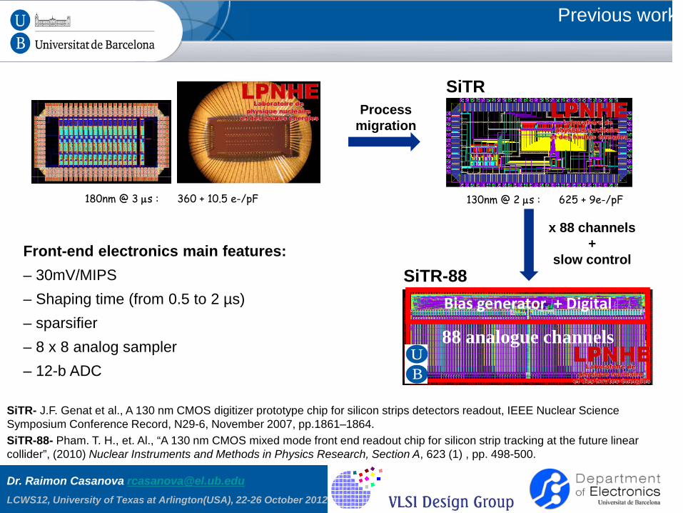
Previous work
180nm @ 3 µs : 360 + 10.5 e-/pF 130nm @ 2 µs : 625 + 9e-/pF
88 analogue channels
Bias generator + Digital
SiTR- J.F. Genat et al., A 130 nm CMOS digitizer prototype chip for silicon strips detectors readout, IEEE Nuclear ScienceSymposium Conference Record, N29-6, November 2007, pp.1861–1864.SiTR-88- Pham. T. H., et. Al., “A 130 nm CMOS mixed mode front end readout chip for silicon strip tracking at the future linear collider”, (2010) Nuclear Instruments and Methods in Physics Research, Section A, 623 (1) , pp. 498-500.
SiTR-88
x 88 channels+
slow control
Processmigration
SiTR
Front-end electronics main features:– 30mV/MIPS– Shaping time (from 0.5 to 2 µs)– sparsifier– 8 x 8 analog sampler– 12-b ADC
Dr. Raimon Casanova [email protected], University of Texas at Arlington(USA), 22-26 October 2012
o SiLC timeline
SiTR-88-130UMC
(1st mixed signal chip)
2007 2008 2009 2010 2011
FPA2008-05979-C04-02 AIDA
LNPHE/IN2P3-CNRSStart of collaboration
with IN2P3Design of the digital part
Complete new design(responsability of UB)
Definition of new architecture
FPA2008-04122-E
FPA2010-21549-C04-01
o DEPFET collaboration timeline for Belle II
DHPv12009 2010 2011
FPA2008-05979-C04-02 FPA2010-21549-C04-01
Slow control JTAG (digital)Analog blocks for configuration
and basic blocks (bandgap, DAC, ADC, amplifier)
T sensor included, IBM 90nm
LAST RUN!!!
2012
TSMC 65T indep current source
current steering DAC-8b
DHPv2 DHPTv1 DHPTv2
TSMC 65T sensor
Dr. Oscar Alonso (FPA2010), Dr. Raimon Casanova (post-doc UB),Dr. Angel Diéguez (UB professor)
Andreu Montiel (AIDA), Dr. Oscar Alonso (FPA2010), Dr. Raimon Casanova (post-doc UB), Dr. Angel Diéguez (UB professor)
UB past work
Dr. Raimon Casanova [email protected], University of Texas at Arlington(USA), 22-26 October 2012
Framework, status
o Front-end electronics main features:o S/N = 25000 e-/1000e-~ 25
o Low noise preamplifiers, preamplifier+shaper
o Linearity 1%, calibration on-chip, DR 100MIPs
o Coarse sampling @ 150-300ns for BCO tagging.
o Shaping time (from 0.5 to 3 µs, depending the strip length)
o Analog sampling, Analog pipelines
o Trigger decision, digitalization, sparsification
o Low power:
o lossless compression
o Dynamic power management
o DSM process
o 256 channels (+pitch adapter)
o Fault tolerant
Dr. Raimon Casanova [email protected], University of Texas at Arlington(USA), 22-26 October 2012
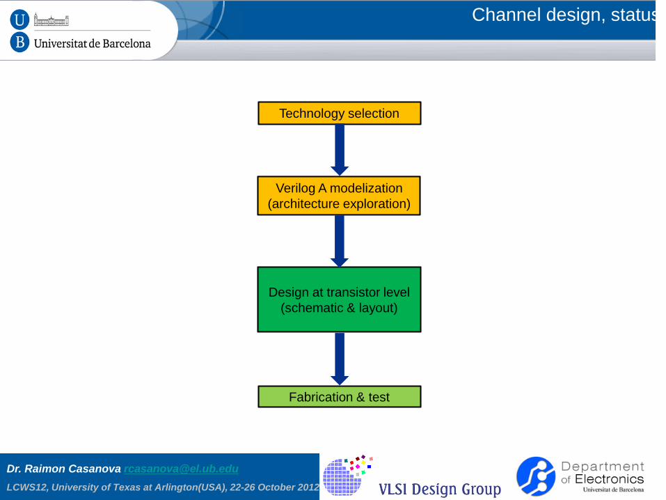
Verilog A modelization(architecture exploration)
Design at transistor level(schematic & layout)
Fabrication & test
Technology selection
Channel design, status
Dr. Raimon Casanova [email protected], University of Texas at Arlington(USA), 22-26 October 2012
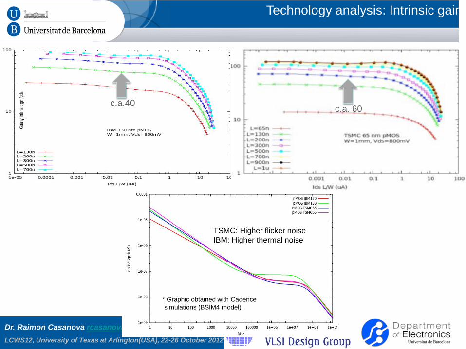
Technology analysis: Intrinsic gain
TSMC: Higher flicker noiseIBM: Higher thermal noise
* Graphic obtained with Cadencesimulations (BSIM4 model).
c.a.40 c.a. 60
Dr. Raimon Casanova [email protected], University of Texas at Arlington(USA), 22-26 October 2012
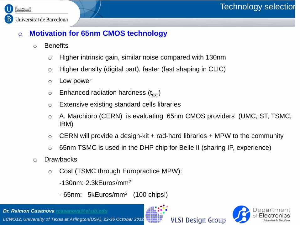
Technology selection
o Motivation for 65nm CMOS technologyo Benefits
o Higher intrinsic gain, similar noise compared with 130nm
o Higher density (digital part), faster (fast shaping in CLIC)
o Low power
o Enhanced radiation hardness (tox )
o Extensive existing standard cells libraries
o A. Marchioro (CERN) is evaluating 65nm CMOS providers (UMC, ST, TSMC, IBM)
o CERN will provide a design-kit + rad-hard libraries + MPW to the community
o 65nm TSMC is used in the DHP chip for Belle II (sharing IP, experience)
o Drawbacks
o Cost (TSMC through Europractice MPW):
-130nm: 2.3kEuros/mm2
- 65nm: 5kEuros/mm2 (100 chips!)
Dr. Raimon Casanova [email protected], University of Texas at Arlington(USA), 22-26 October 2012
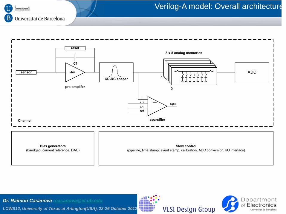
Verilog-A model: Overall architecture
Dr. Raimon Casanova [email protected], University of Texas at Arlington(USA), 22-26 October 2012
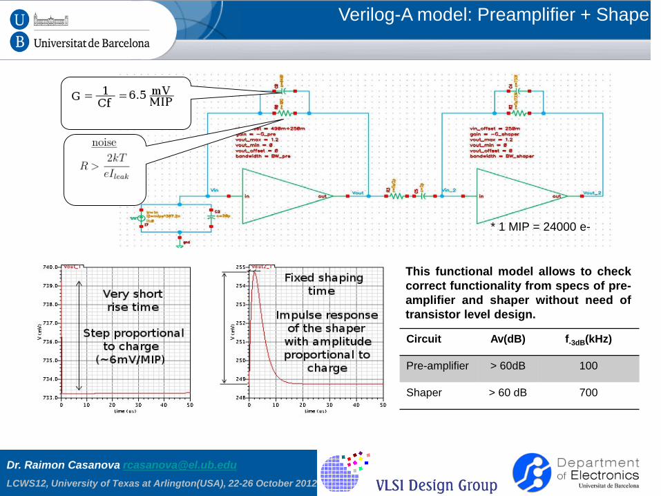
Verilog-A model: Preamplifier + Shaper
* 1 MIP = 24000 e-
This functional model allows to checkcorrect functionality from specs of pre-amplifier and shaper without need oftransistor level design.
Circuit Av(dB) f-3dB(kHz)
Pre-amplifier > 60dB 100
Shaper > 60 dB 700
Dr. Raimon Casanova [email protected], University of Texas at Arlington(USA), 22-26 October 2012
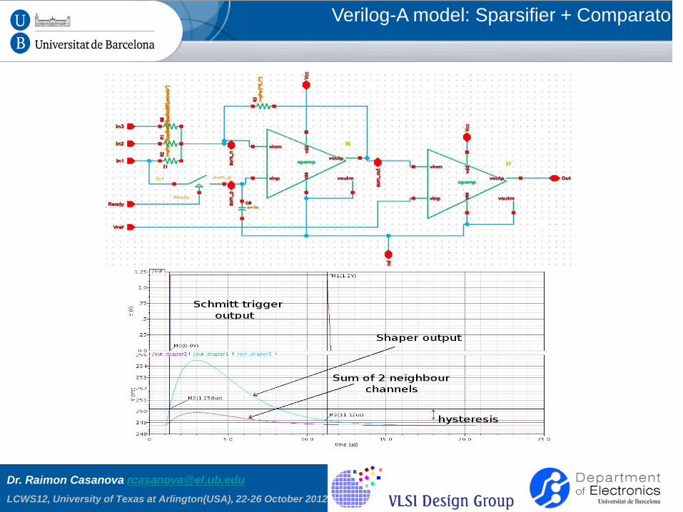
Verilog-A model: Sparsifier + Comparator
Dr. Raimon Casanova [email protected], University of Texas at Arlington(USA), 22-26 October 2012
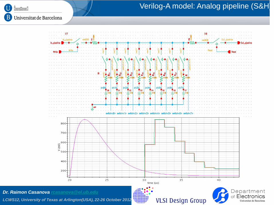
Verilog-A model: Analog pipeline (S&H)
Dr. Raimon Casanova [email protected], University of Texas at Arlington(USA), 22-26 October 2012
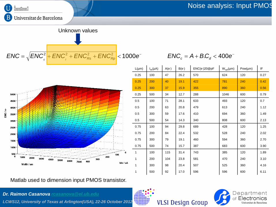
Noise analysis: Input PMOS
L(µm) Ids(µA) A(e-) B(e-) ENC(e-)20@pF Wopt(µm) Pow(µm) IF
0.25 100 47 26.2 570 624 120 0.27
0.25 200 40 19.1 422 781 240 0.42
0.25 300 37 15.9 355 890 360 0.56
0.25 500 34 12.7 288 1046 600 0.79
0.5 100 71 28.1 633 493 120 0.7
0.5 200 63 20.8 479 613 240 1.12
0.5 300 59 17.6 410 694 360 1.49
0.5 500 54 14.3 340 808 600 2.13
0.75 100 94 29.8 689 428 120 1.25
0.75 200 84 22.4 532 528 240 2.02
0.75 300 79 19.1 460 594 360 2.70
0.75 500 74 15.7 387 683 600 3.90
1 100 115 31.4 743 385 120 1.89
1 200 104 23.8 581 470 240 3.10
1 300 98 20.4 507 525 360 4.16
1 500 92 17.0 596 596 600 6.11
−<+= eCBAENC dc 400.−<+++= eENCENCENCENCENC RpRsIc10002222
Unknown values
Matlab used to dimension input PMOS transistor.
Dr. Raimon Casanova [email protected], University of Texas at Arlington(USA), 22-26 October 2012
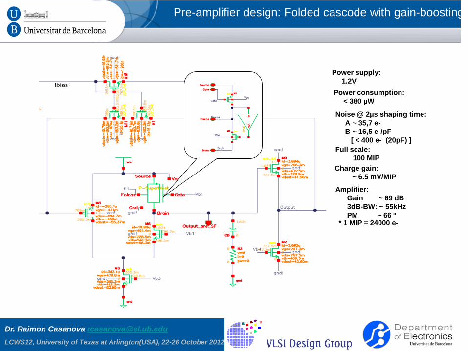
Pre-amplifier design: Folded cascode with gain-boosting
Power consumption:< 380 µW
Noise @ 2µs shaping time:A ~ 35,7 e-B ~ 16,5 e-/pF
[ < 400 e- (20pF) ]
Charge gain:~ 6.5 mV/MIP
* 1 MIP = 24000 e-
Full scale:100 MIP
Amplifier:Gain ~ 69 dB3dB-BW: ~ 55kHzPM ~ 66 º
Power supply:1.2V
Dr. Raimon Casanova [email protected], University of Texas at Arlington(USA), 22-26 October 2012
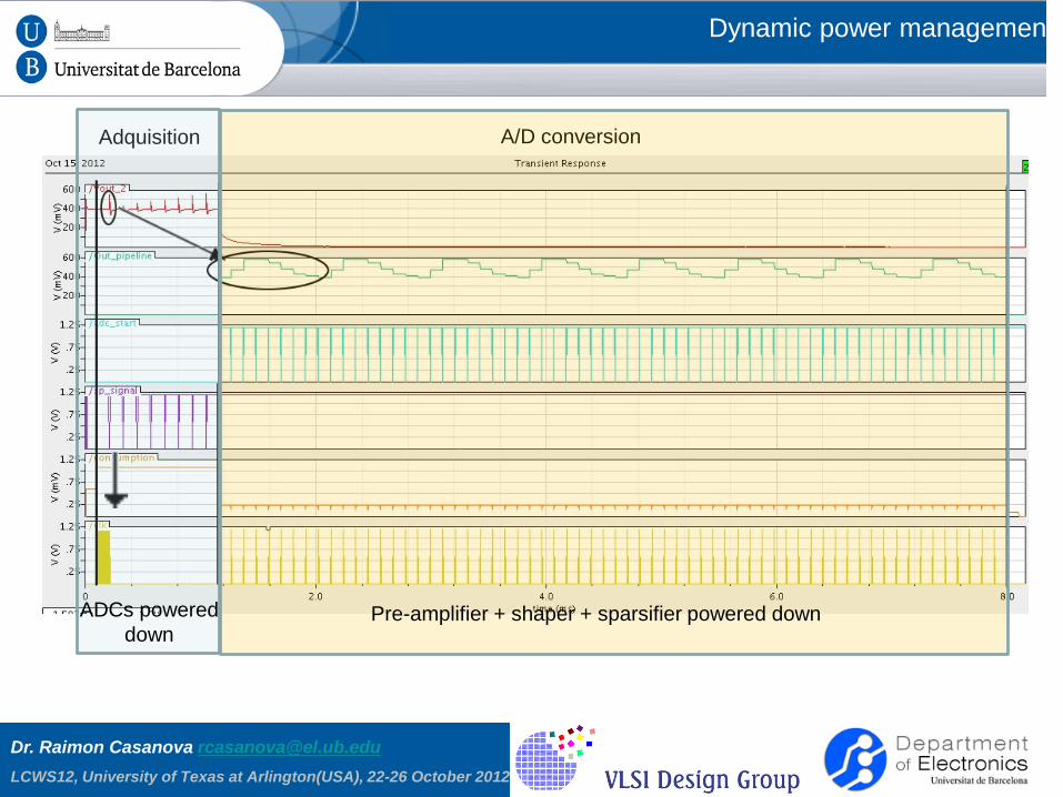
Dynamic power management
Adquisition A/D conversion
ADCs powereddown
Pre-amplifier + shaper + sparsifier powered down
Dr. Raimon Casanova [email protected], University of Texas at Arlington(USA), 22-26 October 2012
Verilog A model of a complete channel designed for architectural exploration: Extraction of main blocks requirements.
10 – 100 faster than spice model
Less accurate but useful to speed up verification of 256 channel chip design
Initiated the design on 65nm TSMC, with synergies with concurrent designs: Designed pre-amplifier at transistor level
Silicon proved auxiliary modules: current source, DAC, temperature sensor.
Dynamic power management under study. How this might affect power supply? Help
needed.
Resources are very limited and implication of other groups is necessary (LPNHE, g-
2@JPARC. …)
Conclusions