Embed Size (px)
Citation preview
Through Glass Via (TGV) Solutions for Wafer and
Chip level Interposers and RF Integration Methods for
High Frequency Applications
Tim Mobley Vern Stygar

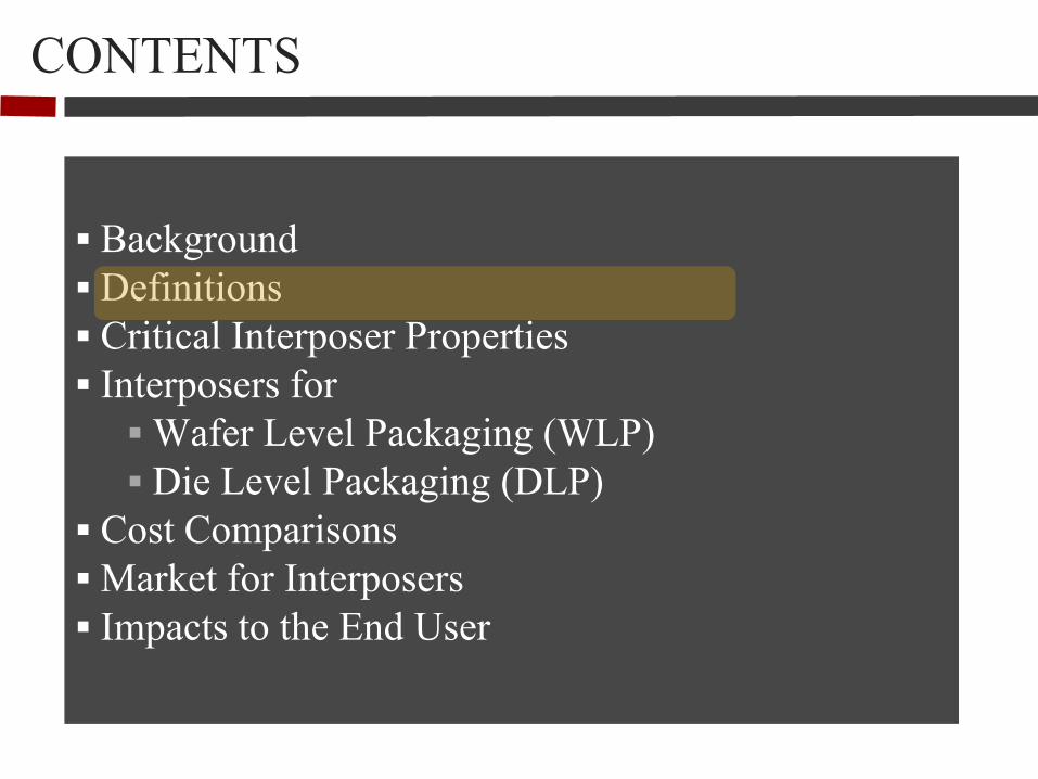
CONTENTS
Background Definitions Critical Interposer Properties Interposers for Wafer Level Packaging (WLP) Die Level Packaging (DLP)
Cost Comparisons Market for Interposers Impacts to the End User
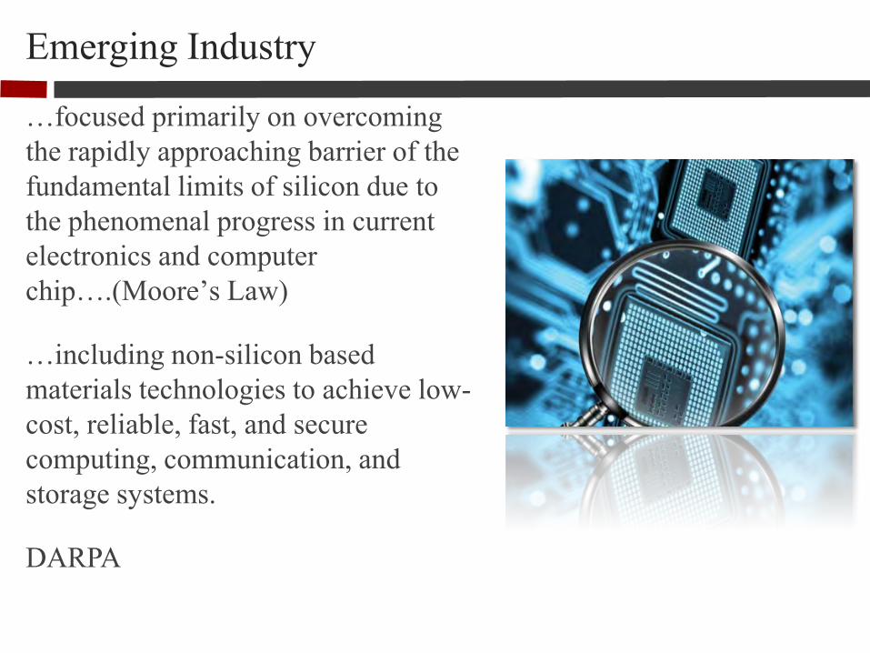
…focused primarily on overcoming the rapidly approaching barrier of the fundamental limits of silicon due to the phenomenal progress in current electronics and computer chip….(Moore’s Law)
…including non-silicon based materials technologies to achieve low-cost, reliable, fast, and secure computing, communication, and storage systems.
DARPA
Emerging Industry
How to make the interconnect from the IC to the Outside World
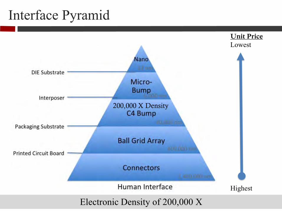
Interface Pyramid Unit Price Lowest Highest
200,000 X Density
Electronic Density of 200,000 X
Why is Density & Interfaces Important?
Integration at the top of pyramid leads to lowest unit price
Cycle time for lowest unit price is the longest
Interfaces drive cost because:
- Unique tooling
- Technical expertise
- Test & manufacturing equipment
Higher density chips are being introduced into the market for memory, processors, and wireless
Presently, solutions at Printed Circuit Board level occupy the most real estate

Solution
Interface reduction Leads to faster cycle time & size reduction
Hermetic package Improves quality over time
Integrated solution Leads to lowest unit price
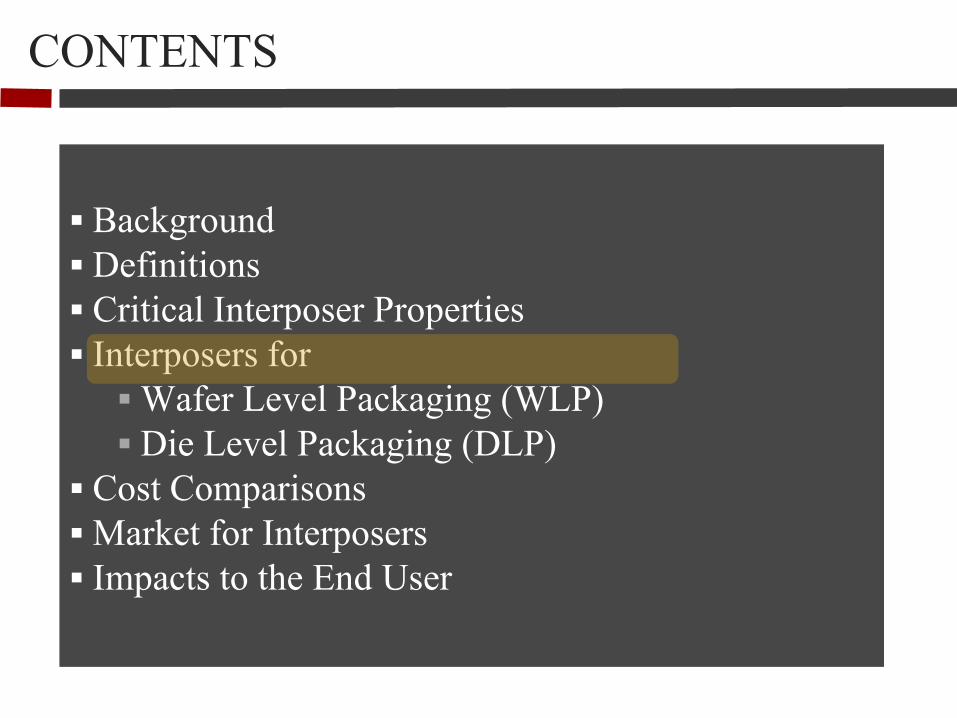
CONTENTS
Background Definitions Critical Interposer Properties Interposers for Wafer Level Packaging (WLP) Die Level Packaging (DLP)
Cost Comparisons Market for Interposers Impacts to the End User
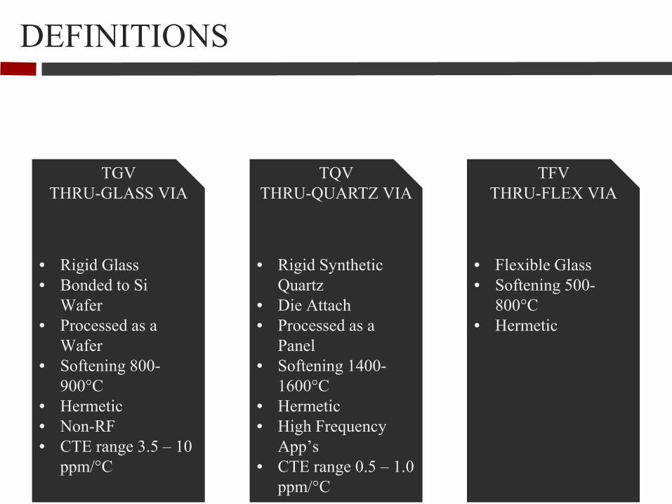
DEFINITIONS
TGV THRU-GLASS VIA
• Rigid Glass • Bonded to Si
Wafer • Processed as a
Wafer • Softening 800-
900°C • Hermetic • Non-RF • CTE range 3.5 – 10
ppm/°C
TQV THRU-QUARTZ VIA
• Rigid Synthetic Quartz
• Die Attach • Processed as a
Panel • Softening 1400-
1600°C • Hermetic • High Frequency
App’s • CTE range 0.5 – 1.0
ppm/°C
TFV THRU-FLEX VIA
• Flexible Glass • Softening 500-
800°C • Hermetic
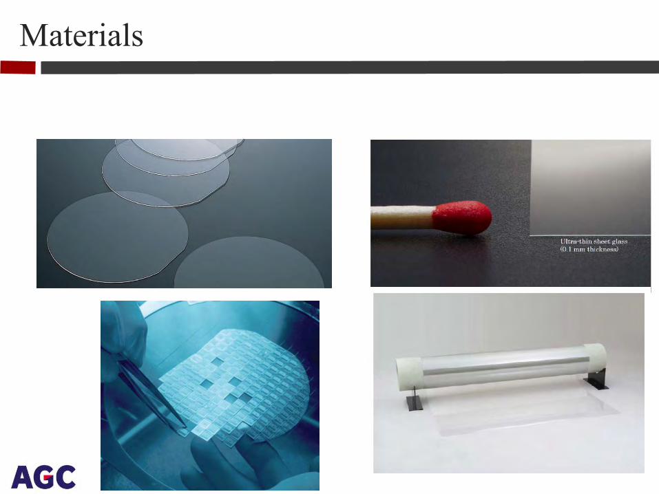
Materials

CONTENTS
Background Definitions Critical Interposer Properties Interposers for Wafer Level Packaging (WLP) Die Level Packaging (DLP)
Cost Comparisons Market for Interposers Impacts to the End User

Materials
CONTENTS
Background Definitions Critical Interposer Properties Interposers for Wafer Level Packaging (WLP) Die Level Packaging (DLP)
Cost Comparisons Market for Interposers Impacts to the End User

nMode TGV/TQV INTERPOSER PROCESS FLOW
Material
• Substrate/Wafer Selection based on Electrical Performance & Design rules • Polish to Specified Thickness • Deposit Anodic Bond Layer
Via • Drill Vias • Inspect
Via Fill • Fill Vias with TCE match Cu • Polish Vias to surface of Glass
Circuit • Add Cu (or standard Thin Film metals) to surfaces • Pattern as required by the Design
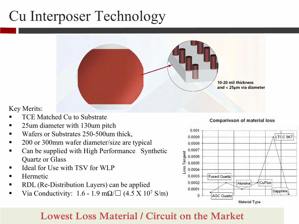
Cu Interposer Technology
Lowest Loss Material / Circuit on the Market
Key Merits: TCE Matched Cu to Substrate 25um diameter with 130um pitch Wafers or Substrates 250-500um thick, 200 or 300mm wafer diameter/size are typical Can be supplied with High Performance Synthetic
Quartz or Glass Ideal for Use with TSV for WLP Hermetic RDL (Re-Distribution Layers) can be applied Via Conductivity: 1.6 - 1.9 mΩ/☐ (4.5 X 10⁷ S/m)
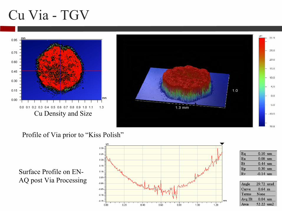
Cu Via - TGV
Cu Density and Size
Profile of Via prior to “Kiss Polish”
Surface Profile on EN-AQ post Via Processing

EMBEDDED RF COMPONENTS

Substrates, Patterns, and Vias
Interposer Performance
...Low loss like Sapphire
...Low cost like PTFE laminates

TGV - Non-Filled Via
250um thick substrate Largest via is 15mils diameter Smallest via is 2mils diameter Exit and Entry side are within 1% of each other
2mil Diameter
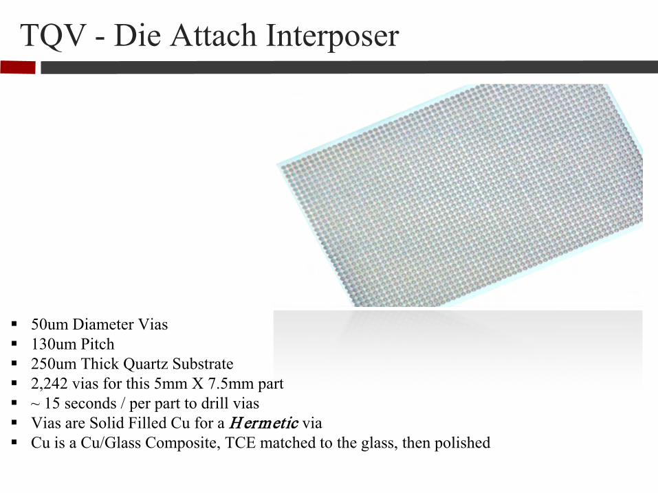
TQV - Die Attach Interposer
50um Diameter Vias 130um Pitch 250um Thick Quartz Substrate 2,242 vias for this 5mm X 7.5mm part ~ 15 seconds / per part to drill vias Vias are Solid Filled Cu for a H ermetic via Cu is a Cu/Glass Composite, TCE matched to the glass, then polished
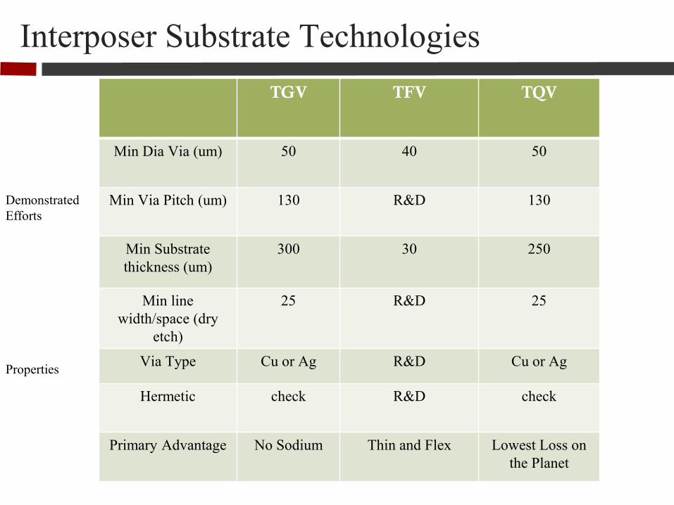
Interposer Substrate Technologies
TGV TFV TQV
Min Dia Via (um) 50 40 50
Min Via Pitch (um) 130 R&D 130
Min Substrate thickness (um)
300 30 250
Min line width/space (dry
etch)
25 R&D 25
Via Type Cu or Ag R&D Cu or Ag
Hermetic check R&D check
Primary Advantage No Sodium Thin and Flex Lowest Loss on the Planet
Demonstrated Efforts
Properties
CONTENTS
Background Definitions Critical Interposer Properties Interposers for Wafer Level Packaging (WLP) Die Level Packaging (DLP)
Cost Comparisons Market for Interposers Impacts to the End User
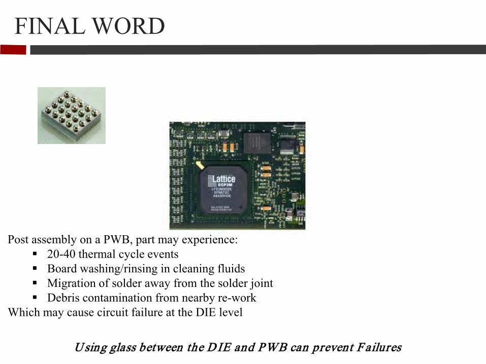
FINAL WORD
Post assembly on a PWB, part may experience: 20-40 thermal cycle events Board washing/rinsing in cleaning fluids Migration of solder away from the solder joint Debris contamination from nearby re-work
Which may cause circuit failure at the DIE level
U sing glass between the D IE and PWB can prevent F ailures
Questions: Contact Us
Vern Stygar [email protected]
Tim Mobley [email protected]
1840 East River Road, Suite 201 Tucson, AZ 85718
520-209-1556
www.nmodesolutions.com
4375 NW 235th St Hillsboro, OR 97124
714-745-3193
www.agcem.com