Embed Size (px)
Citation preview
Affirma RF Simulator User Guide
Product Version 4.4.6April 2001
1994-2001 Cadence Design Systems, Inc. All rights reserved.Printed in the United States of America.
Cadence Design Systems, Inc., 555 River Oaks Parkway, San Jose, CA 95134, USA
Trademarks: Trademarks and service marks of Cadence Design Systems, Inc. (Cadence) contained in thisdocument are attributed to Cadence with the appropriate symbol. For queries regarding Cadence’s trademarks,contact the corporate legal department at the address shown above or call 1-800-862-4522.
All other trademarks are the property of their respective holders.
Restricted Print Permission: This publication is protected by copyright and any unauthorized use of thispublication may violate copyright, trademark, and other laws. Except as specified in this permission statement,this publication may not be copied, reproduced, modified, published, uploaded, posted, transmitted, ordistributed in any way, without prior written permission from Cadence. This statement grants you permission toprint one (1) hard copy of this publication subject to the following conditions:
1. The publication may be used solely for personal, informational, and noncommercial purposes;2. The publication may not be modified in any way;3. Any copy of the publication or portion thereof must include all original copyright, trademark, and other
proprietary notices and this permission statement; and4. Cadence reserves the right to revoke this authorization at any time, and any such use shall be
discontinued immediately upon written notice from Cadence.
Disclaimer: Information in this publication is subject to change without notice and does not represent acommitment on the part of Cadence. The information contained herein is the proprietary and confidentialinformation of Cadence or its licensors, and is supplied subject to, and may be used only by Cadence’s customerin accordance with, a written agreement between Cadence and its customer. Except as may be explicitly setforth in such agreement, Cadence does not make, and expressly disclaims, any representations or warrantiesas to the completeness, accuracy or usefulness of the information contained in this document. Cadence doesnot warrant that use of such information will not infringe any third party rights, nor does Cadence assume anyliability for damages or costs of any kind that may result from use of such information.
Restricted Rights: Use, duplication, or disclosure by the Government is subject to restrictions as set forth inFAR52.227-14 and DFAR252.227-7013 et seq. or its successor.
Affirma RF Simulator (SpectreRF) User Guide
Contents
Preface ............................................................................................................................... 19
Related Documents . . . . . . . . . . . . . . . . . . . . . . . . . . . . . . . . . . . . . . . . . . . . . . . . . . . . . 19
1
SpectreRF Anal yses . . . . . . . . . . . . . . . . . . . . . . . . . . . . . . . . . . . . . . . . . . . . . . . . . . . . 20
Periodic Large-Signal Analysis . . . . . . . . . . . . . . . . . . . . . . . . . . . . . . . . . . . . . . . . . . . . 21Periodicity Assumption . . . . . . . . . . . . . . . . . . . . . . . . . . . . . . . . . . . . . . . . . . . . . . . . 22Linearity Assumption . . . . . . . . . . . . . . . . . . . . . . . . . . . . . . . . . . . . . . . . . . . . . . . . . 22
Periodic Moderate-Signal Analysis (Pdisto) . . . . . . . . . . . . . . . . . . . . . . . . . . . . . . . . . . . 23Large and Moderate Signals in Periodic Distortion Analysis . . . . . . . . . . . . . . . . . . . 23Periodicity Not Assumed . . . . . . . . . . . . . . . . . . . . . . . . . . . . . . . . . . . . . . . . . . . . . . 23Linearity Assumption . . . . . . . . . . . . . . . . . . . . . . . . . . . . . . . . . . . . . . . . . . . . . . . . . 23
Periodic Small-Signal Analysis . . . . . . . . . . . . . . . . . . . . . . . . . . . . . . . . . . . . . . . . . . . . 23Fundamental Assumptions for the Periodic Small-Signal Analyses . . . . . . . . . . . . . . 25
Description of SpectreRF Analyses . . . . . . . . . . . . . . . . . . . . . . . . . . . . . . . . . . . . . . . . . 25Periodic Steady-State Analysis . . . . . . . . . . . . . . . . . . . . . . . . . . . . . . . . . . . . . . . . . 26Periodic Distortion Analysis (Pdisto) . . . . . . . . . . . . . . . . . . . . . . . . . . . . . . . . . . . . . 29Periodic AC Analysis . . . . . . . . . . . . . . . . . . . . . . . . . . . . . . . . . . . . . . . . . . . . . . . . . 32Intermodulation Distortion Computation . . . . . . . . . . . . . . . . . . . . . . . . . . . . . . . . . . . 34Periodic S-Parameter Analysis . . . . . . . . . . . . . . . . . . . . . . . . . . . . . . . . . . . . . . . . . . 36Periodic Transfer Function Analysis . . . . . . . . . . . . . . . . . . . . . . . . . . . . . . . . . . . . . . 40Periodic Noise Analysis . . . . . . . . . . . . . . . . . . . . . . . . . . . . . . . . . . . . . . . . . . . . . . . 43Noise Figure . . . . . . . . . . . . . . . . . . . . . . . . . . . . . . . . . . . . . . . . . . . . . . . . . . . . . . . . 46Flicker Noise . . . . . . . . . . . . . . . . . . . . . . . . . . . . . . . . . . . . . . . . . . . . . . . . . . . . . . . . 47Quasi-Periodic Noise Analysis . . . . . . . . . . . . . . . . . . . . . . . . . . . . . . . . . . . . . . . . . . 49Envelope Following Analysis . . . . . . . . . . . . . . . . . . . . . . . . . . . . . . . . . . . . . . . . . . . 52
April 2001 2 Product Version 4.4.6
Affirma RF Simulator (SpectreRF) User Guide
2
SpectreRF Sim ulation Forms . . . . . . . . . . . . . . . . . . . . . . . . . . . . . . . . . . . . . . . . . . . . 55
Choosing Analyses Form . . . . . . . . . . . . . . . . . . . . . . . . . . . . . . . . . . . . . . . . . . . . . . . . . 55For Periodic Steady-State (PSS) Analysis (Top) . . . . . . . . . . . . . . . . . . . . . . . . . . . . 56For Periodic Steady-State (PSS) Analysis (Bottom) . . . . . . . . . . . . . . . . . . . . . . . . . . 57Modification for Periodic Steady State (PSS) Analysis Sweep (Bottom) . . . . . . . . . . 58For Periodic Distortion (Pdisto) Analysis . . . . . . . . . . . . . . . . . . . . . . . . . . . . . . . . . . 59For Periodic AC (PAC) Analysis with PSS . . . . . . . . . . . . . . . . . . . . . . . . . . . . . . . . . 60Modification for Periodic AC Analysis (PAC) with PSS Sweep . . . . . . . . . . . . . . . . . . 61For Periodic Noise Analysis (Pnoise) with PSS . . . . . . . . . . . . . . . . . . . . . . . . . . . . . 62Modification for Periodic Noise Analysis (Pnoise) with PSS Sweep . . . . . . . . . . . . . . 63For Periodic Transfer Function (PXF) Analysis with PSS . . . . . . . . . . . . . . . . . . . . . . 64Modification for Periodic Transfer Function (PXF) Analysis with PSS Sweep . . . . . . 65For Periodic S-Parameter (PSP) Analysis with PSS . . . . . . . . . . . . . . . . . . . . . . . . . 66Modification for Periodic S-Parameter (PSP) Analysis with PSS Sweep . . . . . . . . . . 67For Quasi-Periodic Noise (QPnoise) Analysis with Pdisto . . . . . . . . . . . . . . . . . . . . . 68For Envelope Following Analysis . . . . . . . . . . . . . . . . . . . . . . . . . . . . . . . . . . . . . . . . 69
Options Forms . . . . . . . . . . . . . . . . . . . . . . . . . . . . . . . . . . . . . . . . . . . . . . . . . . . . . . . . . 70PSS Analysis Options Form (Top) . . . . . . . . . . . . . . . . . . . . . . . . . . . . . . . . . . . . . . . 70PSS Analysis Options Form (Bottom) . . . . . . . . . . . . . . . . . . . . . . . . . . . . . . . . . . . . 71Pdisto Analysis Options Form (Top) . . . . . . . . . . . . . . . . . . . . . . . . . . . . . . . . . . . . . . 72Pdisto Analysis Options Form (Bottom) . . . . . . . . . . . . . . . . . . . . . . . . . . . . . . . . . . . 73PAC Analysis Options Form . . . . . . . . . . . . . . . . . . . . . . . . . . . . . . . . . . . . . . . . . . . . 74PXF Analysis Options Form . . . . . . . . . . . . . . . . . . . . . . . . . . . . . . . . . . . . . . . . . . . . 75Pnoise Analysis Options Form . . . . . . . . . . . . . . . . . . . . . . . . . . . . . . . . . . . . . . . . . . 76PSP Analysis Options Form . . . . . . . . . . . . . . . . . . . . . . . . . . . . . . . . . . . . . . . . . . . . 77QPnoise Analysis Options Form . . . . . . . . . . . . . . . . . . . . . . . . . . . . . . . . . . . . . . . . 78Envelope Following Analysis Options Form (Top) . . . . . . . . . . . . . . . . . . . . . . . . . . . 79Envelope Following Analysis Options Form (bottom) . . . . . . . . . . . . . . . . . . . . . . . . . 80
Results Forms . . . . . . . . . . . . . . . . . . . . . . . . . . . . . . . . . . . . . . . . . . . . . . . . . . . . . . . . . 81Spectral Plots and Time Waveforms . . . . . . . . . . . . . . . . . . . . . . . . . . . . . . . . . . . . . 81PSS Results Form . . . . . . . . . . . . . . . . . . . . . . . . . . . . . . . . . . . . . . . . . . . . . . . . . . . 83Pdisto Results Form . . . . . . . . . . . . . . . . . . . . . . . . . . . . . . . . . . . . . . . . . . . . . . . . . . 87PAC Results Form (with Swept PSS) . . . . . . . . . . . . . . . . . . . . . . . . . . . . . . . . . . . . . 90Pnoise Results Form (with PSS) . . . . . . . . . . . . . . . . . . . . . . . . . . . . . . . . . . . . . . . . 92
April 2001 3 Product Version 4.4.6
Affirma RF Simulator (SpectreRF) User Guide
PXF Results Form (with PSS) . . . . . . . . . . . . . . . . . . . . . . . . . . . . . . . . . . . . . . . . . . 93PSP Results Form (with PSS) . . . . . . . . . . . . . . . . . . . . . . . . . . . . . . . . . . . . . . . . . . 95Envelope Following Results Form . . . . . . . . . . . . . . . . . . . . . . . . . . . . . . . . . . . . . . . 96QPnoise Results Form (with Pdisto) . . . . . . . . . . . . . . . . . . . . . . . . . . . . . . . . . . . . . 98
Form Field Descriptions . . . . . . . . . . . . . . . . . . . . . . . . . . . . . . . . . . . . . . . . . . . . . . . . . . 99Choosing Analysis Form . . . . . . . . . . . . . . . . . . . . . . . . . . . . . . . . . . . . . . . . . . . . . . 99Options Forms . . . . . . . . . . . . . . . . . . . . . . . . . . . . . . . . . . . . . . . . . . . . . . . . . . . . . 123Results Forms . . . . . . . . . . . . . . . . . . . . . . . . . . . . . . . . . . . . . . . . . . . . . . . . . . . . . 130
3
Setting Up f or the Examples . . . . . . . . . . . . . . . . . . . . . . . . . . . . . . . . . . . . . . . . . . . . 140
Setting Up the Software . . . . . . . . . . . . . . . . . . . . . . . . . . . . . . . . . . . . . . . . . . . . . . . . . 140Copying the SpectreRF Simulator Examples . . . . . . . . . . . . . . . . . . . . . . . . . . . . . . 140Setting Up the Cadence Libraries . . . . . . . . . . . . . . . . . . . . . . . . . . . . . . . . . . . . . . 140
4
Simulating Mix ers . . . . . . . . . . . . . . . . . . . . . . . . . . . . . . . . . . . . . . . . . . . . . . . . . . . . . 143
The ne600p Mixer Circuit . . . . . . . . . . . . . . . . . . . . . . . . . . . . . . . . . . . . . . . . . . . . . . . . 144Simulating the ne600p Mixer . . . . . . . . . . . . . . . . . . . . . . . . . . . . . . . . . . . . . . . . . . . . . 146
Opening the ne600p Mixer Circuit in the Schematic Window. . . . . . . . . . . . . . . . . . 146Choosing Simulator Options . . . . . . . . . . . . . . . . . . . . . . . . . . . . . . . . . . . . . . . . . . . 147Setting Up Model Libraries . . . . . . . . . . . . . . . . . . . . . . . . . . . . . . . . . . . . . . . . . . . . 149Setting Design Variables . . . . . . . . . . . . . . . . . . . . . . . . . . . . . . . . . . . . . . . . . . . . . 150
Harmonic Distortion Measurement with PSS . . . . . . . . . . . . . . . . . . . . . . . . . . . . . . . . 151Setting Up the Simulation . . . . . . . . . . . . . . . . . . . . . . . . . . . . . . . . . . . . . . . . . . . . . 151Editing the Schematic . . . . . . . . . . . . . . . . . . . . . . . . . . . . . . . . . . . . . . . . . . . . . . . . 152Setting Up the PSS Analysis . . . . . . . . . . . . . . . . . . . . . . . . . . . . . . . . . . . . . . . . . . 153Running the Simulation . . . . . . . . . . . . . . . . . . . . . . . . . . . . . . . . . . . . . . . . . . . . . . 155Calculating Harmonic Distortion . . . . . . . . . . . . . . . . . . . . . . . . . . . . . . . . . . . . . . . . 156
Noise Figure Measurement with PSS and Pnoise . . . . . . . . . . . . . . . . . . . . . . . . . . . . . 160Setting Up the Simulation . . . . . . . . . . . . . . . . . . . . . . . . . . . . . . . . . . . . . . . . . . . . . 160Editing The Schematic . . . . . . . . . . . . . . . . . . . . . . . . . . . . . . . . . . . . . . . . . . . . . . . 160Setting up the PSS and Pnoise Analyses . . . . . . . . . . . . . . . . . . . . . . . . . . . . . . . . 161Running the Simulation . . . . . . . . . . . . . . . . . . . . . . . . . . . . . . . . . . . . . . . . . . . . . . 163Plotting the Noise Figure . . . . . . . . . . . . . . . . . . . . . . . . . . . . . . . . . . . . . . . . . . . . . 164
April 2001 4 Product Version 4.4.6
Affirma RF Simulator (SpectreRF) User Guide
Noise Figure Measurement and Periodic S-Parameter Plots with PSS and PSP . . . . . 165Setting Up the Simulation . . . . . . . . . . . . . . . . . . . . . . . . . . . . . . . . . . . . . . . . . . . . . 166Editing the Schematic . . . . . . . . . . . . . . . . . . . . . . . . . . . . . . . . . . . . . . . . . . . . . . . . 166Setting up the PSS and PSP Analyses . . . . . . . . . . . . . . . . . . . . . . . . . . . . . . . . . . 168Running the Simulation . . . . . . . . . . . . . . . . . . . . . . . . . . . . . . . . . . . . . . . . . . . . . . 174Plotting the Noise Figure . . . . . . . . . . . . . . . . . . . . . . . . . . . . . . . . . . . . . . . . . . . . . 174Plotting Periodic S-Parameters . . . . . . . . . . . . . . . . . . . . . . . . . . . . . . . . . . . . . . . . . 176
Conversion Gain Measurement with PSS and PXF . . . . . . . . . . . . . . . . . . . . . . . . . . . . 180Setting Up the Simulation . . . . . . . . . . . . . . . . . . . . . . . . . . . . . . . . . . . . . . . . . . . . . 180Editing the Schematic . . . . . . . . . . . . . . . . . . . . . . . . . . . . . . . . . . . . . . . . . . . . . . . . 180Setting Up the PSS and PXF Analyses . . . . . . . . . . . . . . . . . . . . . . . . . . . . . . . . . . 181Running the Simulation . . . . . . . . . . . . . . . . . . . . . . . . . . . . . . . . . . . . . . . . . . . . . . 184Plotting the Conversion Gain . . . . . . . . . . . . . . . . . . . . . . . . . . . . . . . . . . . . . . . . . . 185Plotting the Power Supply Rejection . . . . . . . . . . . . . . . . . . . . . . . . . . . . . . . . . . . . . 188
Calculating the 1 dB Compression Point with Swept PSS . . . . . . . . . . . . . . . . . . . . . . . 188Setting Up the Simulation . . . . . . . . . . . . . . . . . . . . . . . . . . . . . . . . . . . . . . . . . . . . . 188Editing the Schematic . . . . . . . . . . . . . . . . . . . . . . . . . . . . . . . . . . . . . . . . . . . . . . . . 189Setting Up the Swept PSS Analysis . . . . . . . . . . . . . . . . . . . . . . . . . . . . . . . . . . . . . 189Running the Simulation . . . . . . . . . . . . . . . . . . . . . . . . . . . . . . . . . . . . . . . . . . . . . . 191Plotting the 1 dB Compression Point . . . . . . . . . . . . . . . . . . . . . . . . . . . . . . . . . . . . 192
Third-Order Intercept Measurement with Swept PSS and PAC . . . . . . . . . . . . . . . . . . . 194Setting Up the Simulation . . . . . . . . . . . . . . . . . . . . . . . . . . . . . . . . . . . . . . . . . . . . . 195Editing the Schematic . . . . . . . . . . . . . . . . . . . . . . . . . . . . . . . . . . . . . . . . . . . . . . . . 195Setting Up the PSS and PAC Analyses . . . . . . . . . . . . . . . . . . . . . . . . . . . . . . . . . . 196Running the Simulation . . . . . . . . . . . . . . . . . . . . . . . . . . . . . . . . . . . . . . . . . . . . . . 199Plotting the IP3 Curve . . . . . . . . . . . . . . . . . . . . . . . . . . . . . . . . . . . . . . . . . . . . . . . 200
Intermodulation Distortion Measurement with Pdisto . . . . . . . . . . . . . . . . . . . . . . . . . . 202Setting Up the Simulation . . . . . . . . . . . . . . . . . . . . . . . . . . . . . . . . . . . . . . . . . . . . . 203Editing the Schematic . . . . . . . . . . . . . . . . . . . . . . . . . . . . . . . . . . . . . . . . . . . . . . . . 203Setting Up the Pdisto Analysis . . . . . . . . . . . . . . . . . . . . . . . . . . . . . . . . . . . . . . . . . 204Selecting Simulation Outputs . . . . . . . . . . . . . . . . . . . . . . . . . . . . . . . . . . . . . . . . . . 206Running the Simulation . . . . . . . . . . . . . . . . . . . . . . . . . . . . . . . . . . . . . . . . . . . . . . 207Plotting the Voltage and Power . . . . . . . . . . . . . . . . . . . . . . . . . . . . . . . . . . . . . . . . . 208
Noise Figure with Pdisto and QPnoise . . . . . . . . . . . . . . . . . . . . . . . . . . . . . . . . . . . . . 211Setting Up the Simulation . . . . . . . . . . . . . . . . . . . . . . . . . . . . . . . . . . . . . . . . . . . . . 211Editing the Schematic . . . . . . . . . . . . . . . . . . . . . . . . . . . . . . . . . . . . . . . . . . . . . . . . 211
April 2001 5 Product Version 4.4.6
Affirma RF Simulator (SpectreRF) User Guide
Setting Up the Pdisto and QPnoise Analyses . . . . . . . . . . . . . . . . . . . . . . . . . . . . . 213Selecting Simulation Outputs . . . . . . . . . . . . . . . . . . . . . . . . . . . . . . . . . . . . . . . . . . 219Running the Simulation . . . . . . . . . . . . . . . . . . . . . . . . . . . . . . . . . . . . . . . . . . . . . . 220Plotting the Noise Figure . . . . . . . . . . . . . . . . . . . . . . . . . . . . . . . . . . . . . . . . . . . . . 220Plotting the Output Noise . . . . . . . . . . . . . . . . . . . . . . . . . . . . . . . . . . . . . . . . . . . . . 222
5
Simulating Oscillator s . . . . . . . . . . . . . . . . . . . . . . . . . . . . . . . . . . . . . . . . . . . . . . . . . 225
Autonomous PSS Analysis . . . . . . . . . . . . . . . . . . . . . . . . . . . . . . . . . . . . . . . . . . . . 225Phases of Autonomous PSS Analysis . . . . . . . . . . . . . . . . . . . . . . . . . . . . . . . . . . . 225Phase Noise and Oscillators . . . . . . . . . . . . . . . . . . . . . . . . . . . . . . . . . . . . . . . . . . 226Starting the Oscillator . . . . . . . . . . . . . . . . . . . . . . . . . . . . . . . . . . . . . . . . . . . . . . . . 226Stabilizing the Oscillator . . . . . . . . . . . . . . . . . . . . . . . . . . . . . . . . . . . . . . . . . . . . . . 226
About the tline3oscRF Example . . . . . . . . . . . . . . . . . . . . . . . . . . . . . . . . . . . . . . . . . 227Simulating tline3oscRF . . . . . . . . . . . . . . . . . . . . . . . . . . . . . . . . . . . . . . . . . . . . . . 227Analysis Setup . . . . . . . . . . . . . . . . . . . . . . . . . . . . . . . . . . . . . . . . . . . . . . . . . . . . . 232Running the Simulation . . . . . . . . . . . . . . . . . . . . . . . . . . . . . . . . . . . . . . . . . . . . . . 237Plotting the Fundamental Frequency . . . . . . . . . . . . . . . . . . . . . . . . . . . . . . . . . . . . 237Plotting the Steady State Solution . . . . . . . . . . . . . . . . . . . . . . . . . . . . . . . . . . . . . . 238Plotting the Phase Noise . . . . . . . . . . . . . . . . . . . . . . . . . . . . . . . . . . . . . . . . . . . . . 240
A Balanced, Tunable Differential Oscillator: oscDiff . . . . . . . . . . . . . . . . . . . . . . . . . . . 241Simulating oscDiff . . . . . . . . . . . . . . . . . . . . . . . . . . . . . . . . . . . . . . . . . . . . . . . . . . 242Analysis Setup . . . . . . . . . . . . . . . . . . . . . . . . . . . . . . . . . . . . . . . . . . . . . . . . . . . . . 246Editing Design Variables . . . . . . . . . . . . . . . . . . . . . . . . . . . . . . . . . . . . . . . . . . . . . . 250Running the Simulation . . . . . . . . . . . . . . . . . . . . . . . . . . . . . . . . . . . . . . . . . . . . . . 251Plotting the Fundamental Frequency . . . . . . . . . . . . . . . . . . . . . . . . . . . . . . . . . . . . 251
Troubleshooting for Oscillators . . . . . . . . . . . . . . . . . . . . . . . . . . . . . . . . . . . . . . . . . . . . 254
6
Simulating Lo w-Noise Amplifier s . . . . . . . . . . . . . . . . . . . . . . . . . . . . . . . . . . . . . . . 256
Types of Analysis Shown in this Chapter . . . . . . . . . . . . . . . . . . . . . . . . . . . . . . . . . . . . 256Procedures for Simulating the LNA Example . . . . . . . . . . . . . . . . . . . . . . . . . . . . . . . . . 256
Choosing Simulator Options . . . . . . . . . . . . . . . . . . . . . . . . . . . . . . . . . . . . . . . . . . . 259Setting Up Model Libraries . . . . . . . . . . . . . . . . . . . . . . . . . . . . . . . . . . . . . . . . . . . . 261
April 2001 6 Product Version 4.4.6
Affirma RF Simulator (SpectreRF) User Guide
Voltage Gain Calculation and Output Voltage Distribution . . . . . . . . . . . . . . . . . . . . . . . 261Editing Schematic . . . . . . . . . . . . . . . . . . . . . . . . . . . . . . . . . . . . . . . . . . . . . . . . . . . 261Analysis Setup . . . . . . . . . . . . . . . . . . . . . . . . . . . . . . . . . . . . . . . . . . . . . . . . . . . . . 262Running Simulation . . . . . . . . . . . . . . . . . . . . . . . . . . . . . . . . . . . . . . . . . . . . . . . . . 263Plotting Voltage Gain . . . . . . . . . . . . . . . . . . . . . . . . . . . . . . . . . . . . . . . . . . . . . . . . 264Output Voltage Distribution . . . . . . . . . . . . . . . . . . . . . . . . . . . . . . . . . . . . . . . . . . . . 266Editing Schematic . . . . . . . . . . . . . . . . . . . . . . . . . . . . . . . . . . . . . . . . . . . . . . . . . . . 266Analysis Setup . . . . . . . . . . . . . . . . . . . . . . . . . . . . . . . . . . . . . . . . . . . . . . . . . . . . . 267Running the Simulation . . . . . . . . . . . . . . . . . . . . . . . . . . . . . . . . . . . . . . . . . . . . . . 269Plotting Output Voltage Distribution . . . . . . . . . . . . . . . . . . . . . . . . . . . . . . . . . . . . . 270
S-Parameter Analysis for Low Noise Amplifiers . . . . . . . . . . . . . . . . . . . . . . . . . . . . . . . 272Editing the Schematic . . . . . . . . . . . . . . . . . . . . . . . . . . . . . . . . . . . . . . . . . . . . . . . . 272Analysis Setup . . . . . . . . . . . . . . . . . . . . . . . . . . . . . . . . . . . . . . . . . . . . . . . . . . . . . 273Running Simulation . . . . . . . . . . . . . . . . . . . . . . . . . . . . . . . . . . . . . . . . . . . . . . . . . 274Plotting S-Parameters . . . . . . . . . . . . . . . . . . . . . . . . . . . . . . . . . . . . . . . . . . . . . . . 274Plotting the Voltage Standing Wave Ratio . . . . . . . . . . . . . . . . . . . . . . . . . . . . . . . . 278
Linear Two-Port Noise Analysis . . . . . . . . . . . . . . . . . . . . . . . . . . . . . . . . . . . . . . . . . . . 279Editing the Schematic . . . . . . . . . . . . . . . . . . . . . . . . . . . . . . . . . . . . . . . . . . . . . . . . 279Analysis Setup . . . . . . . . . . . . . . . . . . . . . . . . . . . . . . . . . . . . . . . . . . . . . . . . . . . . . 280Running the Simulation . . . . . . . . . . . . . . . . . . . . . . . . . . . . . . . . . . . . . . . . . . . . . . 281Plotting the Noise Figure and Minimum Noise Figure . . . . . . . . . . . . . . . . . . . . . . . 282Plotting the Equivalent Noise Resistance . . . . . . . . . . . . . . . . . . . . . . . . . . . . . . . . . 285Plotting Load and Source Stability Circles . . . . . . . . . . . . . . . . . . . . . . . . . . . . . . . . 286Plotting the Noise Circles . . . . . . . . . . . . . . . . . . . . . . . . . . . . . . . . . . . . . . . . . . . . . 290
Noise Calculations Using Pnoise . . . . . . . . . . . . . . . . . . . . . . . . . . . . . . . . . . . . . . . . . . 292Editing the Schematic . . . . . . . . . . . . . . . . . . . . . . . . . . . . . . . . . . . . . . . . . . . . . . . . 293Analysis Setup . . . . . . . . . . . . . . . . . . . . . . . . . . . . . . . . . . . . . . . . . . . . . . . . . . . . . 293Running the Simulation . . . . . . . . . . . . . . . . . . . . . . . . . . . . . . . . . . . . . . . . . . . . . . 296Plotting the Noise Calculations . . . . . . . . . . . . . . . . . . . . . . . . . . . . . . . . . . . . . . . . . 297
Plotting the 1dB Compression Point . . . . . . . . . . . . . . . . . . . . . . . . . . . . . . . . . . . . . . . 301Editing the Schematic . . . . . . . . . . . . . . . . . . . . . . . . . . . . . . . . . . . . . . . . . . . . . . . . 302Analysis Setup . . . . . . . . . . . . . . . . . . . . . . . . . . . . . . . . . . . . . . . . . . . . . . . . . . . . . 302Running the Simulation . . . . . . . . . . . . . . . . . . . . . . . . . . . . . . . . . . . . . . . . . . . . . . 304Plotting the 1dB Compression Point . . . . . . . . . . . . . . . . . . . . . . . . . . . . . . . . . . . . . 305
Plotting the Third-Order Intercept Point . . . . . . . . . . . . . . . . . . . . . . . . . . . . . . . . . . . . . 307Editing the Schematic . . . . . . . . . . . . . . . . . . . . . . . . . . . . . . . . . . . . . . . . . . . . . . . . 307
April 2001 7 Product Version 4.4.6
Affirma RF Simulator (SpectreRF) User Guide
Analysis Setup . . . . . . . . . . . . . . . . . . . . . . . . . . . . . . . . . . . . . . . . . . . . . . . . . . . . . 308Running the Simulation . . . . . . . . . . . . . . . . . . . . . . . . . . . . . . . . . . . . . . . . . . . . . . 309Plotting the Third-Order Intercept Point . . . . . . . . . . . . . . . . . . . . . . . . . . . . . . . . . . 310
Plotting Conversion Gain and Power Supply Rejection . . . . . . . . . . . . . . . . . . . . . . . . . 312Editing the Schematic . . . . . . . . . . . . . . . . . . . . . . . . . . . . . . . . . . . . . . . . . . . . . . . . 312Analysis Setup . . . . . . . . . . . . . . . . . . . . . . . . . . . . . . . . . . . . . . . . . . . . . . . . . . . . . 313Running Simulation . . . . . . . . . . . . . . . . . . . . . . . . . . . . . . . . . . . . . . . . . . . . . . . . . 316Plotting Conversion Gain and Power Supply Rejection . . . . . . . . . . . . . . . . . . . . . . 316
7
Simulating T ransmission Lines . . . . . . . . . . . . . . . . . . . . . . . . . . . . . . . . . . . . . . . . . 320
Use Model One: Using the LMG Visual Interface . . . . . . . . . . . . . . . . . . . . . . . . . . . . . 320Use Model Two: Modeling Transmission Lines Without the Visual Interface . . . . . . . . . 321The Transmission Line Model Generator Form . . . . . . . . . . . . . . . . . . . . . . . . . . . . . . . 322
Menus . . . . . . . . . . . . . . . . . . . . . . . . . . . . . . . . . . . . . . . . . . . . . . . . . . . . . . . . . . . . 322Display Section . . . . . . . . . . . . . . . . . . . . . . . . . . . . . . . . . . . . . . . . . . . . . . . . . . . . . 325Data Entry Section . . . . . . . . . . . . . . . . . . . . . . . . . . . . . . . . . . . . . . . . . . . . . . . . . . 325Function Buttons . . . . . . . . . . . . . . . . . . . . . . . . . . . . . . . . . . . . . . . . . . . . . . . . . . . 326Default Values . . . . . . . . . . . . . . . . . . . . . . . . . . . . . . . . . . . . . . . . . . . . . . . . . . . . . 326
Example of Modeling a Transmission Line Using LMG . . . . . . . . . . . . . . . . . . . . . . . . . 327Setup . . . . . . . . . . . . . . . . . . . . . . . . . . . . . . . . . . . . . . . . . . . . . . . . . . . . . . . . . . . . 327Creating the Transmission Line Model . . . . . . . . . . . . . . . . . . . . . . . . . . . . . . . . . . . 327Using Macromodels Created Externally by LMG . . . . . . . . . . . . . . . . . . . . . . . . . . . 334
Example of Automatically Creating a Transmission Line . . . . . . . . . . . . . . . . . . . . . . . . 338Accuracy of the LMG Macromodels . . . . . . . . . . . . . . . . . . . . . . . . . . . . . . . . . . . . . . . . 340
8
Modeling RF IC P ackages . . . . . . . . . . . . . . . . . . . . . . . . . . . . . . . . . . . . . . . . . . . . . . 345
The Four PKG Building Blocks . . . . . . . . . . . . . . . . . . . . . . . . . . . . . . . . . . . . . . . . . . . 347Package Physical Geometry Modeling . . . . . . . . . . . . . . . . . . . . . . . . . . . . . . . . . . . 347EM Solvers and Mesh Making . . . . . . . . . . . . . . . . . . . . . . . . . . . . . . . . . . . . . . . . . 349Macromodel Generation . . . . . . . . . . . . . . . . . . . . . . . . . . . . . . . . . . . . . . . . . . . . . . 349
PKG Setup Requirements . . . . . . . . . . . . . . . . . . . . . . . . . . . . . . . . . . . . . . . . . . . . . . . 350License Checking . . . . . . . . . . . . . . . . . . . . . . . . . . . . . . . . . . . . . . . . . . . . . . . . . . . 350Executables . . . . . . . . . . . . . . . . . . . . . . . . . . . . . . . . . . . . . . . . . . . . . . . . . . . . . . . 350
April 2001 8 Product Version 4.4.6
Affirma RF Simulator (SpectreRF) User Guide
PKG GUI Files . . . . . . . . . . . . . . . . . . . . . . . . . . . . . . . . . . . . . . . . . . . . . . . . . . . . . 350Initialization Files . . . . . . . . . . . . . . . . . . . . . . . . . . . . . . . . . . . . . . . . . . . . . . . . . . . 350Running pkg . . . . . . . . . . . . . . . . . . . . . . . . . . . . . . . . . . . . . . . . . . . . . . . . . . . . . . . 351
The PKG RF IC Package Modeler Window . . . . . . . . . . . . . . . . . . . . . . . . . . . . . . . . . . 351Menu Buttons . . . . . . . . . . . . . . . . . . . . . . . . . . . . . . . . . . . . . . . . . . . . . . . . . . . . . . 352Function Buttons . . . . . . . . . . . . . . . . . . . . . . . . . . . . . . . . . . . . . . . . . . . . . . . . . . . 354
Package Dimension Setup . . . . . . . . . . . . . . . . . . . . . . . . . . . . . . . . . . . . . . . . . . . . . . . 355QFP Packages . . . . . . . . . . . . . . . . . . . . . . . . . . . . . . . . . . . . . . . . . . . . . . . . . . . . . 355Data Entries for QFP Packages . . . . . . . . . . . . . . . . . . . . . . . . . . . . . . . . . . . . . . . . 356SOIC Packages . . . . . . . . . . . . . . . . . . . . . . . . . . . . . . . . . . . . . . . . . . . . . . . . . . . . 358Data Entries for SOIC Packages . . . . . . . . . . . . . . . . . . . . . . . . . . . . . . . . . . . . . . . 358DIP Packages . . . . . . . . . . . . . . . . . . . . . . . . . . . . . . . . . . . . . . . . . . . . . . . . . . . . . . 359Data Entries for DIP Packages . . . . . . . . . . . . . . . . . . . . . . . . . . . . . . . . . . . . . . . . . 360
Die Attach Setup . . . . . . . . . . . . . . . . . . . . . . . . . . . . . . . . . . . . . . . . . . . . . . . . . . . . . . 361Data Entries for SOIC Packages . . . . . . . . . . . . . . . . . . . . . . . . . . . . . . . . . . . . . . . 362
Internal Lead Frame Setup . . . . . . . . . . . . . . . . . . . . . . . . . . . . . . . . . . . . . . . . . . . . . . 362Menu Buttons . . . . . . . . . . . . . . . . . . . . . . . . . . . . . . . . . . . . . . . . . . . . . . . . . . . . . . 362Function Buttons . . . . . . . . . . . . . . . . . . . . . . . . . . . . . . . . . . . . . . . . . . . . . . . . . . . 363Data Entries for the Internal Lead Frame Setup . . . . . . . . . . . . . . . . . . . . . . . . . . . . 364More about Using Symmetry . . . . . . . . . . . . . . . . . . . . . . . . . . . . . . . . . . . . . . . . . . 365Lead Frame File Format . . . . . . . . . . . . . . . . . . . . . . . . . . . . . . . . . . . . . . . . . . . . . . 365
Bond Wire Setup . . . . . . . . . . . . . . . . . . . . . . . . . . . . . . . . . . . . . . . . . . . . . . . . . . . . . . 367Menu Buttons . . . . . . . . . . . . . . . . . . . . . . . . . . . . . . . . . . . . . . . . . . . . . . . . . . . . . . 367Function Buttons . . . . . . . . . . . . . . . . . . . . . . . . . . . . . . . . . . . . . . . . . . . . . . . . . . . 367Data Entries for the Bond Wire Setup . . . . . . . . . . . . . . . . . . . . . . . . . . . . . . . . . . . 369Bond Wire Configurations . . . . . . . . . . . . . . . . . . . . . . . . . . . . . . . . . . . . . . . . . . . . 370Bond Wire File Format . . . . . . . . . . . . . . . . . . . . . . . . . . . . . . . . . . . . . . . . . . . . . . . 371Save the Current Setting . . . . . . . . . . . . . . . . . . . . . . . . . . . . . . . . . . . . . . . . . . . . . 372
Parameter Extraction . . . . . . . . . . . . . . . . . . . . . . . . . . . . . . . . . . . . . . . . . . . . . . . . . . . 372Capacitance Calculation . . . . . . . . . . . . . . . . . . . . . . . . . . . . . . . . . . . . . . . . . . . . . . 373Inductance Calculation . . . . . . . . . . . . . . . . . . . . . . . . . . . . . . . . . . . . . . . . . . . . . . . 375Function Buttons for Parameter Extraction . . . . . . . . . . . . . . . . . . . . . . . . . . . . . . . . 377
Macromodel Generation . . . . . . . . . . . . . . . . . . . . . . . . . . . . . . . . . . . . . . . . . . . . . . . . 377Data Entries and Buttons for Macromodel Generation . . . . . . . . . . . . . . . . . . . . . . . 377Die Attach Terminal . . . . . . . . . . . . . . . . . . . . . . . . . . . . . . . . . . . . . . . . . . . . . . . . . 378Macromodel Schematic . . . . . . . . . . . . . . . . . . . . . . . . . . . . . . . . . . . . . . . . . . . . . . 379
April 2001 9 Product Version 4.4.6
Affirma RF Simulator (SpectreRF) User Guide
High Frequency Resonance Damping for the Spectre Simulator . . . . . . . . . . . . . . . 380Accuracy Analysis . . . . . . . . . . . . . . . . . . . . . . . . . . . . . . . . . . . . . . . . . . . . . . . . . . 381Simulation of Package Models in the Affirma Analog Circuit Design Environment . 381Example of Package Modeling With a Mixer Using PKG . . . . . . . . . . . . . . . . . . . . . 385
9
Extracting K-Models . . . . . . . . . . . . . . . . . . . . . . . . . . . . . . . . . . . . . . . . . . . . . . . . . . . 409
Procedures for Simulating k_mod_extraction_example . . . . . . . . . . . . . . . . . . . . . . 410Analysis Setup . . . . . . . . . . . . . . . . . . . . . . . . . . . . . . . . . . . . . . . . . . . . . . . . . . . . . 417Running the Simulation . . . . . . . . . . . . . . . . . . . . . . . . . . . . . . . . . . . . . . . . . . . . . . 424Checking the Simulation Results . . . . . . . . . . . . . . . . . . . . . . . . . . . . . . . . . . . . . . . 424Creating the K-Model . . . . . . . . . . . . . . . . . . . . . . . . . . . . . . . . . . . . . . . . . . . . . . . . 427More About the K-Model . . . . . . . . . . . . . . . . . . . . . . . . . . . . . . . . . . . . . . . . . . . . . 430K-model data files . . . . . . . . . . . . . . . . . . . . . . . . . . . . . . . . . . . . . . . . . . . . . . . . . . . 436
10
Extracting J-Models . . . . . . . . . . . . . . . . . . . . . . . . . . . . . . . . . . . . . . . . . . . . . . . . . . . 439
Procedures for Simulating j_mod_extraction_example . . . . . . . . . . . . . . . . . . . . . . 439Analysis Setup . . . . . . . . . . . . . . . . . . . . . . . . . . . . . . . . . . . . . . . . . . . . . . . . . . . . . 446Running the Simulation . . . . . . . . . . . . . . . . . . . . . . . . . . . . . . . . . . . . . . . . . . . . . . 451Creating the J-Model . . . . . . . . . . . . . . . . . . . . . . . . . . . . . . . . . . . . . . . . . . . . . . . . 452Using the J-model in a circuit . . . . . . . . . . . . . . . . . . . . . . . . . . . . . . . . . . . . . . . . . . 453More About the J-model . . . . . . . . . . . . . . . . . . . . . . . . . . . . . . . . . . . . . . . . . . . . . . 466
11
Modeling T ransmitter s . . . . . . . . . . . . . . . . . . . . . . . . . . . . . . . . . . . . . . . . . . . . . . . . . 478
Envelope Following . . . . . . . . . . . . . . . . . . . . . . . . . . . . . . . . . . . . . . . . . . . . . . . . . . 478Taking a Closer Look at the Envelope Following Procedure . . . . . . . . . . . . . . . . . . 482Following the Change in the Information (Baseband Signal) Through the Circuit . . 486Plotting the Complete Baseband Signal . . . . . . . . . . . . . . . . . . . . . . . . . . . . . . . . . . 491Plotting the Baseband Trajectory . . . . . . . . . . . . . . . . . . . . . . . . . . . . . . . . . . . . . . . 492Plotting the Transmitted Power Spectral Density for ACPR Calculations . . . . . . . . . 495
Measuring Load Pull Contours and Reflection Coefficients . . . . . . . . . . . . . . . . . . . . . . 504Setting Up and Running the Simulation . . . . . . . . . . . . . . . . . . . . . . . . . . . . . . . . . . 504
April 2001 10 Product Version 4.4.6
Affirma RF Simulator (SpectreRF) User Guide
Displaying Load Contours . . . . . . . . . . . . . . . . . . . . . . . . . . . . . . . . . . . . . . . . . . . . 514Adding the Reflection Contours to the Plot . . . . . . . . . . . . . . . . . . . . . . . . . . . . . . . 517Moving to Differential Mode . . . . . . . . . . . . . . . . . . . . . . . . . . . . . . . . . . . . . . . . . . . 526
Using S-Parameter Input Files . . . . . . . . . . . . . . . . . . . . . . . . . . . . . . . . . . . . . . . . . . . . 527Setting Up the Schematic for the First Simulation . . . . . . . . . . . . . . . . . . . . . . . . . . 527Setting Up and Running the First Simulation . . . . . . . . . . . . . . . . . . . . . . . . . . . . . . 532The S-Parameter File . . . . . . . . . . . . . . . . . . . . . . . . . . . . . . . . . . . . . . . . . . . . . . . . 533Setting Up and Running the Second Simulation . . . . . . . . . . . . . . . . . . . . . . . . . . . 533Using an S-Parameter Input File with a SpectreRF Analysis . . . . . . . . . . . . . . . . . . 538
12
Modeling Spiral Inductor s and Bondpads . . . . . . . . . . . . . . . . . . . . . . . . . . . . . . . . 544
Modeling Spiral Inductors . . . . . . . . . . . . . . . . . . . . . . . . . . . . . . . . . . . . . . . . . . . . . . . 544Process File Preparation . . . . . . . . . . . . . . . . . . . . . . . . . . . . . . . . . . . . . . . . . . . . . 545Spiral Inductor Simulation in the Schematic Flow . . . . . . . . . . . . . . . . . . . . . . . . . . 549Spiral Inductor Modeling under the RF Sub-Menu . . . . . . . . . . . . . . . . . . . . . . . . . . 554Equivalent Circuit Models . . . . . . . . . . . . . . . . . . . . . . . . . . . . . . . . . . . . . . . . . . . . . 556Example . . . . . . . . . . . . . . . . . . . . . . . . . . . . . . . . . . . . . . . . . . . . . . . . . . . . . . . . . . 559
Modeling Bondpads . . . . . . . . . . . . . . . . . . . . . . . . . . . . . . . . . . . . . . . . . . . . . . . . . . . . 569Input to the Modeler . . . . . . . . . . . . . . . . . . . . . . . . . . . . . . . . . . . . . . . . . . . . . . . . . 570Parameter Sets . . . . . . . . . . . . . . . . . . . . . . . . . . . . . . . . . . . . . . . . . . . . . . . . . . . . . 570Modeling Issues . . . . . . . . . . . . . . . . . . . . . . . . . . . . . . . . . . . . . . . . . . . . . . . . . . . . 572LNA Example . . . . . . . . . . . . . . . . . . . . . . . . . . . . . . . . . . . . . . . . . . . . . . . . . . . . . . 573
References for the Bondpad Section . . . . . . . . . . . . . . . . . . . . . . . . . . . . . . . . . . . . . . . 581
13
Behavioral Models and Methods f or Top Do wn Design . . . . . . . . . . . . . . . . . . . . . 582
Top Down Design of RF Systems . . . . . . . . . . . . . . . . . . . . . . . . . . . . . . . . . . . . . . . . . 583Baseband Modeling . . . . . . . . . . . . . . . . . . . . . . . . . . . . . . . . . . . . . . . . . . . . . . . . . . . . 586
Plotting Baseband Equivalent Output Signals for Baseband and Passband Circuits 589About Baseband Modeling . . . . . . . . . . . . . . . . . . . . . . . . . . . . . . . . . . . . . . . . . . . . 590
April 2001 11 Product Version 4.4.6
Affirma RF Simulator (SpectreRF) User Guide
Library Overview . . . . . . . . . . . . . . . . . . . . . . . . . . . . . . . . . . . . . . . . . . . . . . . . . . . . . . 591Warnings You Can Ignore . . . . . . . . . . . . . . . . . . . . . . . . . . . . . . . . . . . . . . . . . . . . . . . 595Use Model and Design Example . . . . . . . . . . . . . . . . . . . . . . . . . . . . . . . . . . . . . . . . . . 596Relationship Between Baseband and Passband Noise . . . . . . . . . . . . . . . . . . . . . . . . . 620Baseband Library . . . . . . . . . . . . . . . . . . . . . . . . . . . . . . . . . . . . . . . . . . . . . . . . . . . . . . 630
Assumptions . . . . . . . . . . . . . . . . . . . . . . . . . . . . . . . . . . . . . . . . . . . . . . . . . . . . . . . 630Compatibility . . . . . . . . . . . . . . . . . . . . . . . . . . . . . . . . . . . . . . . . . . . . . . . . . . . . . . . 631Library Categories . . . . . . . . . . . . . . . . . . . . . . . . . . . . . . . . . . . . . . . . . . . . . . . . . . 631Inputs and Outputs on Baseband Models . . . . . . . . . . . . . . . . . . . . . . . . . . . . . . . . 631Some Parameters Common to Several Models . . . . . . . . . . . . . . . . . . . . . . . . . . . . 632
Library Description . . . . . . . . . . . . . . . . . . . . . . . . . . . . . . . . . . . . . . . . . . . . . . . . . . . . . 651Notes on models involving frequency translation: . . . . . . . . . . . . . . . . . . . . . . . . . . 652Power Amplifier Model . . . . . . . . . . . . . . . . . . . . . . . . . . . . . . . . . . . . . . . . . . . . . . . 653Low Noise Amplifier Baseband Model . . . . . . . . . . . . . . . . . . . . . . . . . . . . . . . . . . . 655IQ Modulator Models . . . . . . . . . . . . . . . . . . . . . . . . . . . . . . . . . . . . . . . . . . . . . . . . 657IQ Demodulator . . . . . . . . . . . . . . . . . . . . . . . . . . . . . . . . . . . . . . . . . . . . . . . . . . . . 664RF-to-IFand IF-to-RF Mixers . . . . . . . . . . . . . . . . . . . . . . . . . . . . . . . . . . . . . . . . . . 672Passive Devices . . . . . . . . . . . . . . . . . . . . . . . . . . . . . . . . . . . . . . . . . . . . . . . . . . . . 679Linear Time Invariant Filters . . . . . . . . . . . . . . . . . . . . . . . . . . . . . . . . . . . . . . . . . . . 687Comparison of baseband and passband models . . . . . . . . . . . . . . . . . . . . . . . . . . . 695BB_Loss . . . . . . . . . . . . . . . . . . . . . . . . . . . . . . . . . . . . . . . . . . . . . . . . . . . . . . . . . . 697Phase Shifter . . . . . . . . . . . . . . . . . . . . . . . . . . . . . . . . . . . . . . . . . . . . . . . . . . . . . . 698Phase Shifter . . . . . . . . . . . . . . . . . . . . . . . . . . . . . . . . . . . . . . . . . . . . . . . . . . . . . . 702Ideal Transformer . . . . . . . . . . . . . . . . . . . . . . . . . . . . . . . . . . . . . . . . . . . . . . . . . . . 709Rectangular-to-Polar Transformation . . . . . . . . . . . . . . . . . . . . . . . . . . . . . . . . . . . . 711Polar-to-Rectangular Transformation . . . . . . . . . . . . . . . . . . . . . . . . . . . . . . . . . . . . 712Instrumentation and Terminating Blocks . . . . . . . . . . . . . . . . . . . . . . . . . . . . . . . . . 713Baseband Drive Signals . . . . . . . . . . . . . . . . . . . . . . . . . . . . . . . . . . . . . . . . . . . . . . 716References . . . . . . . . . . . . . . . . . . . . . . . . . . . . . . . . . . . . . . . . . . . . . . . . . . . . . . . . 723
A
Oscillator Noise Anal ysis . . . . . . . . . . . . . . . . . . . . . . . . . . . . . . . . . . . . . . . . . . . . . . 724
Phase Noise Primer . . . . . . . . . . . . . . . . . . . . . . . . . . . . . . . . . . . . . . . . . . . . . . . . . . . . 725Models for Phase Noise . . . . . . . . . . . . . . . . . . . . . . . . . . . . . . . . . . . . . . . . . . . . . . . . . 728
Linear Time-Invariant (LTI) Models . . . . . . . . . . . . . . . . . . . . . . . . . . . . . . . . . . . . . . 728
April 2001 12 Product Version 4.4.6
Affirma RF Simulator (SpectreRF) User Guide
Linear Time-Varying (LTV) Models . . . . . . . . . . . . . . . . . . . . . . . . . . . . . . . . . . . . . . 729Amplitude Noise and Phase Noise in the “Linear” Model . . . . . . . . . . . . . . . . . . . . . 733Details of the SpectreRF Calculation . . . . . . . . . . . . . . . . . . . . . . . . . . . . . . . . . . . . 734
Calculating Phase Noise . . . . . . . . . . . . . . . . . . . . . . . . . . . . . . . . . . . . . . . . . . . . . . . . 737Setting Simulator Options . . . . . . . . . . . . . . . . . . . . . . . . . . . . . . . . . . . . . . . . . . . . . 737Tips about Getting PSS to Converge . . . . . . . . . . . . . . . . . . . . . . . . . . . . . . . . . . . . 738How to Tell If the Answer Is Correct . . . . . . . . . . . . . . . . . . . . . . . . . . . . . . . . . . . . . 739
Troubleshooting Phase Noise Calculations . . . . . . . . . . . . . . . . . . . . . . . . . . . . . . . . . . 739Known Limitations of the Simulator . . . . . . . . . . . . . . . . . . . . . . . . . . . . . . . . . . . . . 740What Can Go Wrong . . . . . . . . . . . . . . . . . . . . . . . . . . . . . . . . . . . . . . . . . . . . . . . . 740Phase Noise Error Messages . . . . . . . . . . . . . . . . . . . . . . . . . . . . . . . . . . . . . . . . . . 742The tstab Parameter . . . . . . . . . . . . . . . . . . . . . . . . . . . . . . . . . . . . . . . . . . . . . . . . . 743
Frequently Asked Questions . . . . . . . . . . . . . . . . . . . . . . . . . . . . . . . . . . . . . . . . . . . . . 744Further Reading . . . . . . . . . . . . . . . . . . . . . . . . . . . . . . . . . . . . . . . . . . . . . . . . . . . . . . . 749References . . . . . . . . . . . . . . . . . . . . . . . . . . . . . . . . . . . . . . . . . . . . . . . . . . . . . . . . . . . 749
B
Running PSS Anal ysis Eff ectivel y . . . . . . . . . . . . . . . . . . . . . . . . . . . . . . . . . . . . . . . 752
General Convergence Aids . . . . . . . . . . . . . . . . . . . . . . . . . . . . . . . . . . . . . . . . . . . . . . 752The steadyratio and tstab Parameters . . . . . . . . . . . . . . . . . . . . . . . . . . . . . . . . . . . 752Additional Convergence Aids . . . . . . . . . . . . . . . . . . . . . . . . . . . . . . . . . . . . . . . . . . 753
Convergence Aids for Oscillators . . . . . . . . . . . . . . . . . . . . . . . . . . . . . . . . . . . . . . . . . . 754Running PSS Analysis Hierarchically . . . . . . . . . . . . . . . . . . . . . . . . . . . . . . . . . . . . 755
C
Using the psin Component . . . . . . . . . . . . . . . . . . . . . . . . . . . . . . . . . . . . . . . . . . . . . 757
Independent Resistive Source (psin) . . . . . . . . . . . . . . . . . . . . . . . . . . . . . . . . . . . . 757Parameter Types for the psin Component . . . . . . . . . . . . . . . . . . . . . . . . . . . . . . . . 760Name Parameters . . . . . . . . . . . . . . . . . . . . . . . . . . . . . . . . . . . . . . . . . . . . . . . . . . 763psin Instance Parameter . . . . . . . . . . . . . . . . . . . . . . . . . . . . . . . . . . . . . . . . . . . . . . 763General Waveform Parameters . . . . . . . . . . . . . . . . . . . . . . . . . . . . . . . . . . . . . . . . 763Sinusoidal Waveform Parameters . . . . . . . . . . . . . . . . . . . . . . . . . . . . . . . . . . . . . . 764Amplitude Modulation Parameters . . . . . . . . . . . . . . . . . . . . . . . . . . . . . . . . . . . . . . 765FM Modulation Parameters . . . . . . . . . . . . . . . . . . . . . . . . . . . . . . . . . . . . . . . . . . . 767
April 2001 13 Product Version 4.4.6
Affirma RF Simulator (SpectreRF) User Guide
Noise Parameters . . . . . . . . . . . . . . . . . . . . . . . . . . . . . . . . . . . . . . . . . . . . . . . . . . . 770Port Parameters . . . . . . . . . . . . . . . . . . . . . . . . . . . . . . . . . . . . . . . . . . . . . . . . . . . . 771Temperature Effect Parameters . . . . . . . . . . . . . . . . . . . . . . . . . . . . . . . . . . . . . . . . 771Small-Signal Parameters . . . . . . . . . . . . . . . . . . . . . . . . . . . . . . . . . . . . . . . . . . . . . 772Additional Notes . . . . . . . . . . . . . . . . . . . . . . . . . . . . . . . . . . . . . . . . . . . . . . . . . . . . 774
D
The RF Librar y . . . . . . . . . . . . . . . . . . . . . . . . . . . . . . . . . . . . . . . . . . . . . . . . . . . . . . . . 775
Top-Down Design Elements . . . . . . . . . . . . . . . . . . . . . . . . . . . . . . . . . . . . . . . . . . . . . . 775Filter . . . . . . . . . . . . . . . . . . . . . . . . . . . . . . . . . . . . . . . . . . . . . . . . . . . . . . . . . . . . . 777Balun . . . . . . . . . . . . . . . . . . . . . . . . . . . . . . . . . . . . . . . . . . . . . . . . . . . . . . . . . . . . 780Low Noise Amplifier . . . . . . . . . . . . . . . . . . . . . . . . . . . . . . . . . . . . . . . . . . . . . . . . . 780Mixer . . . . . . . . . . . . . . . . . . . . . . . . . . . . . . . . . . . . . . . . . . . . . . . . . . . . . . . . . . . . . 783Power Amplifier . . . . . . . . . . . . . . . . . . . . . . . . . . . . . . . . . . . . . . . . . . . . . . . . . . . . . 787Oscillator . . . . . . . . . . . . . . . . . . . . . . . . . . . . . . . . . . . . . . . . . . . . . . . . . . . . . . . . . 789Quadrature Signal Generator . . . . . . . . . . . . . . . . . . . . . . . . . . . . . . . . . . . . . . . . . . 791Phase Shifter . . . . . . . . . . . . . . . . . . . . . . . . . . . . . . . . . . . . . . . . . . . . . . . . . . . . . . 792
Bottom-Up Design Elements . . . . . . . . . . . . . . . . . . . . . . . . . . . . . . . . . . . . . . . . . . . . . 793Testbench Elements . . . . . . . . . . . . . . . . . . . . . . . . . . . . . . . . . . . . . . . . . . . . . . . . . . . 793
CDMA Signal Source (IS-95 rev_xmit) and Eye-Diagram Generator . . . . . . . . . . . . 794GSM Signal Source (GSM-xmtr) . . . . . . . . . . . . . . . . . . . . . . . . . . . . . . . . . . . . . . . 796P/4-DQPSK Signal Source (pi_over4_dqpsk) . . . . . . . . . . . . . . . . . . . . . . . . . . . . . 798Creating Variations on the Library Baseband Signal Generators Using the Modelwriter801
Uncatagorized Elements . . . . . . . . . . . . . . . . . . . . . . . . . . . . . . . . . . . . . . . . . . . . . . . . 805
E
Plotting Spectre S-P arameter Sim ulation Data . . . . . . . . . . . . . . . . . . . . . . . . . . . . 807
The Equations for the S-Parameter Waveform Calculator in the Affirma Analog CircuitDesign Environment: . . . . . . . . . . . . . . . . . . . . . . . . . . . . . . . . . . . . . . . . . . . . . . . . 807
April 2001 14 Product Version 4.4.6
Affirma RF Simulator (SpectreRF) User Guide
F
Using Pdisto Anal ysis Eff ectivel y . . . . . . . . . . . . . . . . . . . . . . . . . . . . . . . . . . . . . . . 818
When to Use Pdisto Analysis . . . . . . . . . . . . . . . . . . . . . . . . . . . . . . . . . . . . . . . . . . . . . 818Essentials of the MFT Method . . . . . . . . . . . . . . . . . . . . . . . . . . . . . . . . . . . . . . . . . . . . 820Pdisto and PSS Analyses Compared . . . . . . . . . . . . . . . . . . . . . . . . . . . . . . . . . . . . . . 823Pdisto and PAC Analyses Compared . . . . . . . . . . . . . . . . . . . . . . . . . . . . . . . . . . . . . . . 824Pdisto Analysis Parameters . . . . . . . . . . . . . . . . . . . . . . . . . . . . . . . . . . . . . . . . . . . . . . 825Application Examples . . . . . . . . . . . . . . . . . . . . . . . . . . . . . . . . . . . . . . . . . . . . . . . . . . 825
Switched Capacitor Filter Example . . . . . . . . . . . . . . . . . . . . . . . . . . . . . . . . . . . . . 826High-Performance Receiver Example . . . . . . . . . . . . . . . . . . . . . . . . . . . . . . . . . . . 827
Running a Pdisto Analysis . . . . . . . . . . . . . . . . . . . . . . . . . . . . . . . . . . . . . . . . . . . . . . . 829Picking the Large Fundamental . . . . . . . . . . . . . . . . . . . . . . . . . . . . . . . . . . . . . . . . 829Setting Up Sources . . . . . . . . . . . . . . . . . . . . . . . . . . . . . . . . . . . . . . . . . . . . . . . . . 830Sweeping a Pdisto Analysis . . . . . . . . . . . . . . . . . . . . . . . . . . . . . . . . . . . . . . . . . . . 831
Convergence Aids . . . . . . . . . . . . . . . . . . . . . . . . . . . . . . . . . . . . . . . . . . . . . . . . . . . . . 832Memory Management . . . . . . . . . . . . . . . . . . . . . . . . . . . . . . . . . . . . . . . . . . . . . . . . . . 834Dealing with Sub-Harmonics . . . . . . . . . . . . . . . . . . . . . . . . . . . . . . . . . . . . . . . . . . . . . 835Understanding the Narration from the Pdisto Analysis . . . . . . . . . . . . . . . . . . . . . . . . . 835References . . . . . . . . . . . . . . . . . . . . . . . . . . . . . . . . . . . . . . . . . . . . . . . . . . . . . . . . . . . 836
G
An Intr oduction to the PLL librar y . . . . . . . . . . . . . . . . . . . . . . . . . . . . . . . . . . . . . . . 838
The Models in the PLL library . . . . . . . . . . . . . . . . . . . . . . . . . . . . . . . . . . . . . . . . . . 840Introduction . . . . . . . . . . . . . . . . . . . . . . . . . . . . . . . . . . . . . . . . . . . . . . . . . . . . . . . . 840Phase-Domain Model of a Simple PLL . . . . . . . . . . . . . . . . . . . . . . . . . . . . . . . . . . 841Assembling a Model of a PFD-based PLL . . . . . . . . . . . . . . . . . . . . . . . . . . . . . . . . 854How the PFD Model Works. . . . . . . . . . . . . . . . . . . . . . . . . . . . . . . . . . . . . . . . . . . . 864References . . . . . . . . . . . . . . . . . . . . . . . . . . . . . . . . . . . . . . . . . . . . . . . . . . . . . . . . 870
H
Using por t in SpectreRF Sim ulations . . . . . . . . . . . . . . . . . . . . . . . . . . . . . . . . . . . . 872
port Parameter Types . . . . . . . . . . . . . . . . . . . . . . . . . . . . . . . . . . . . . . . . . . . . . . . 873Port Parameters . . . . . . . . . . . . . . . . . . . . . . . . . . . . . . . . . . . . . . . . . . . . . . . . . . . . 876
April 2001 15 Product Version 4.4.6
Affirma RF Simulator (SpectreRF) User Guide
General Waveform Parameters . . . . . . . . . . . . . . . . . . . . . . . . . . . . . . . . . . . . . . . . 876DC Waveform Parameters . . . . . . . . . . . . . . . . . . . . . . . . . . . . . . . . . . . . . . . . . . . . 878Pulse Waveform Parameters . . . . . . . . . . . . . . . . . . . . . . . . . . . . . . . . . . . . . . . . . . 879PWL Waveform Parameters . . . . . . . . . . . . . . . . . . . . . . . . . . . . . . . . . . . . . . . . . . . 881Sinusoidal Waveform Parameters . . . . . . . . . . . . . . . . . . . . . . . . . . . . . . . . . . . . . . 885Exponential Waveform Parameters . . . . . . . . . . . . . . . . . . . . . . . . . . . . . . . . . . . . . 895Noise Parameters . . . . . . . . . . . . . . . . . . . . . . . . . . . . . . . . . . . . . . . . . . . . . . . . . . . 898Small-Signal Parameters . . . . . . . . . . . . . . . . . . . . . . . . . . . . . . . . . . . . . . . . . . . . . 899Temperature Effect Parameters . . . . . . . . . . . . . . . . . . . . . . . . . . . . . . . . . . . . . . . . 902Additional Notes . . . . . . . . . . . . . . . . . . . . . . . . . . . . . . . . . . . . . . . . . . . . . . . . . . . . 903
I
Anal yzing Time-V arying Noise Pr oper ties . . . . . . . . . . . . . . . . . . . . . . . . . . . . . . . . 904
Time-Domain Noise Characterization . . . . . . . . . . . . . . . . . . . . . . . . . . . . . . . . . . . 905Calculating Noise Correlation Coefficients . . . . . . . . . . . . . . . . . . . . . . . . . . . . . . . . 910
J
Using T abulated S-parameter s . . . . . . . . . . . . . . . . . . . . . . . . . . . . . . . . . . . . . . . . . . 913
Using the nport component . . . . . . . . . . . . . . . . . . . . . . . . . . . . . . . . . . . . . . . . . . . . . . 914Controlling Model Accuracy . . . . . . . . . . . . . . . . . . . . . . . . . . . . . . . . . . . . . . . . . . . . . . 914
Using relerr and abserr . . . . . . . . . . . . . . . . . . . . . . . . . . . . . . . . . . . . . . . . . . . . . . . 915Using the ratorder parameter . . . . . . . . . . . . . . . . . . . . . . . . . . . . . . . . . . . . . . . . . . 917
Troubleshooting . . . . . . . . . . . . . . . . . . . . . . . . . . . . . . . . . . . . . . . . . . . . . . . . . . . . . . . 917Assessing the quality of the rational interpolation . . . . . . . . . . . . . . . . . . . . . . . . . . 917
Model Reuse . . . . . . . . . . . . . . . . . . . . . . . . . . . . . . . . . . . . . . . . . . . . . . . . . . . . . . . . . 918References . . . . . . . . . . . . . . . . . . . . . . . . . . . . . . . . . . . . . . . . . . . . . . . . . . . . . . . . . . . 919
K
Using the Calculator IPN Functions f or RF Sim ulations . . . . . . . . . . . . . . . . . . . . 920
How to Use the ipn and ipnVRI Functions . . . . . . . . . . . . . . . . . . . . . . . . . . . . . . . . . . . 920Setting Up . . . . . . . . . . . . . . . . . . . . . . . . . . . . . . . . . . . . . . . . . . . . . . . . . . . . . . . . . 920Editing the Schematic . . . . . . . . . . . . . . . . . . . . . . . . . . . . . . . . . . . . . . . . . . . . . . . . 921Setting Up the Analysis . . . . . . . . . . . . . . . . . . . . . . . . . . . . . . . . . . . . . . . . . . . . . . 922
April 2001 16 Product Version 4.4.6
Affirma RF Simulator (SpectreRF) User Guide
Running the Simulation . . . . . . . . . . . . . . . . . . . . . . . . . . . . . . . . . . . . . . . . . . . . . . 926Plotting the IP3 Curve Using Direct Plot . . . . . . . . . . . . . . . . . . . . . . . . . . . . . . . . . . 926Plot IP3 Using the ipn and ipnVRI Buttons in the Waveform Calculator . . . . . . . . . . 930
Using the IPN Function with Scalar Inputs . . . . . . . . . . . . . . . . . . . . . . . . . . . . . . . . . . 934Setting Up . . . . . . . . . . . . . . . . . . . . . . . . . . . . . . . . . . . . . . . . . . . . . . . . . . . . . . . . . 934Setting Up the Analysis . . . . . . . . . . . . . . . . . . . . . . . . . . . . . . . . . . . . . . . . . . . . . . 934Running Simulation . . . . . . . . . . . . . . . . . . . . . . . . . . . . . . . . . . . . . . . . . . . . . . . . . 938Plotting the Single Point IP3 Using the Calculator . . . . . . . . . . . . . . . . . . . . . . . . . . 939
L
Using PSP and Pnoise Anal yses . . . . . . . . . . . . . . . . . . . . . . . . . . . . . . . . . . . . . . . . 942
Overview . . . . . . . . . . . . . . . . . . . . . . . . . . . . . . . . . . . . . . . . . . . . . . . . . . . . . . . . . . . . 942Periodic S-parameters . . . . . . . . . . . . . . . . . . . . . . . . . . . . . . . . . . . . . . . . . . . . . . . . . . 943
Linear Time-Invariant S-Parameters . . . . . . . . . . . . . . . . . . . . . . . . . . . . . . . . . . . . . 943Frequency Translating S-Parameters . . . . . . . . . . . . . . . . . . . . . . . . . . . . . . . . . . . . 944Upper and Lower Sidebands . . . . . . . . . . . . . . . . . . . . . . . . . . . . . . . . . . . . . . . . . . 946
PSP Analysis Example . . . . . . . . . . . . . . . . . . . . . . . . . . . . . . . . . . . . . . . . . . . . . . . . . 946Noise and Noise Parameters . . . . . . . . . . . . . . . . . . . . . . . . . . . . . . . . . . . . . . . . . . . . . 950
Calculating Noise in Linear Time-Invariant (DC Bias) Circuits . . . . . . . . . . . . . . . . . 950Calculating Noise in Time-Varying (Periodic Bias) Circuits . . . . . . . . . . . . . . . . . . . 950The maxsideband Parameter . . . . . . . . . . . . . . . . . . . . . . . . . . . . . . . . . . . . . . . . . . 951Noise Correlation Matrices and Equivalent Noise Sources . . . . . . . . . . . . . . . . . . . 951
Noise Figure . . . . . . . . . . . . . . . . . . . . . . . . . . . . . . . . . . . . . . . . . . . . . . . . . . . . . . . . . 954Performing Noise Figure Computations . . . . . . . . . . . . . . . . . . . . . . . . . . . . . . . . . . 954Noise Figure From Noise and SP Analyses . . . . . . . . . . . . . . . . . . . . . . . . . . . . . . . 955Pnoise (SSB) Noise Figure . . . . . . . . . . . . . . . . . . . . . . . . . . . . . . . . . . . . . . . . . . . 955DSB Noise Figure . . . . . . . . . . . . . . . . . . . . . . . . . . . . . . . . . . . . . . . . . . . . . . . . . . . 957IEEE Noise Figure . . . . . . . . . . . . . . . . . . . . . . . . . . . . . . . . . . . . . . . . . . . . . . . . . . 958
Noise Computation Example . . . . . . . . . . . . . . . . . . . . . . . . . . . . . . . . . . . . . . . . . . . . . 961Input Referred Noise . . . . . . . . . . . . . . . . . . . . . . . . . . . . . . . . . . . . . . . . . . . . . . . . . . . 962
Using Input Referred Noise . . . . . . . . . . . . . . . . . . . . . . . . . . . . . . . . . . . . . . . . . . . 963How IRN is Calculated . . . . . . . . . . . . . . . . . . . . . . . . . . . . . . . . . . . . . . . . . . . . . . . 964Relation to Gain . . . . . . . . . . . . . . . . . . . . . . . . . . . . . . . . . . . . . . . . . . . . . . . . . . . . 966Referring Noise to Ports . . . . . . . . . . . . . . . . . . . . . . . . . . . . . . . . . . . . . . . . . . . . . . 966
April 2001 17 Product Version 4.4.6
Affirma RF Simulator (SpectreRF) User Guide
Gain Calculations . . . . . . . . . . . . . . . . . . . . . . . . . . . . . . . . . . . . . . . . . . . . . . . . . . . . . . 967Definitions of Gain . . . . . . . . . . . . . . . . . . . . . . . . . . . . . . . . . . . . . . . . . . . . . . . . . . 967Gain Calculations in Pnoise . . . . . . . . . . . . . . . . . . . . . . . . . . . . . . . . . . . . . . . . . . . 971Phase Noise . . . . . . . . . . . . . . . . . . . . . . . . . . . . . . . . . . . . . . . . . . . . . . . . . . . . . . . 973
Frequently Asked Questions . . . . . . . . . . . . . . . . . . . . . . . . . . . . . . . . . . . . . . . . . . . . . 974Known Problems and Limitations . . . . . . . . . . . . . . . . . . . . . . . . . . . . . . . . . . . . . . . . . . 977
Dubious AC-Noise Analysis Features . . . . . . . . . . . . . . . . . . . . . . . . . . . . . . . . . . . 977Gain in Pnoise and PSP Analyses Inconsistent . . . . . . . . . . . . . . . . . . . . . . . . . . . . 978Harmonics and Sidebands in PSP, PAC, PXF, and Pnoise Analyses . . . . . . . . . . . . 978
Index ................................................................................................................................. 982
April 2001 18 Product Version 4.4.6
Affirma RF Simulator (SpectreRF) User Guide
April 2001 19 Product Version 4.4.6
Preface
This manual assumes that you are familiar with RF circuit design and that you have somefamiliarity with SPICE simulation. It contains information about the Affirma™ RF circuitsimulator as it is used within the Affirma analog circuit design environment. The Affirma RFcircuit simulator is also known as SpectreRF in the software and in this manual.
SpectreRF analyses support the efficient calculation of the operating point, transfer function,noise, and distortion of common RF and communication circuits, such as mixers, oscillators,sample and holds, and switched capacitor filters.
Related Documents
The following documents can give you more information about SpectreRF and relatedproducts.
To learn more about the Affirma analog circuit design environment, consult the AffirmaAnalog Circuit Design Environment User Guide.
To learn more about SpectreRF theoretical concepts, see SpectreRF Theory.
Affirma RF Simulator (SpectreRF) User Guide
1SpectreRF Analyses
The SpectreRF analyses add new capabilities to Spectre simulation, such as direct, efficientcomputation of steady-state solutions and simulation of circuits that translate frequency. Youuse the SpectreRF simulator analyses in combination with the Fourier analysis capability ofSpectre simulation and with the SpectreHDL behavioral modeling language.
The SpectreRF analyses add several kinds of functionality to Spectre simulation.
Periodic Steady-State (PSS) analysis
Periodic Small-Signal analyses
Periodic AC (PAC) analysis
Periodic S-Parameter (PSP) analysis
Periodic Transfer Function (PXF) analysis
Periodic Noise (Pnoise) analysis
Periodic Distortion (Pdisto) analysis
Quasi-Periodic Noise (QPnoise) analysis
Envelope Following analysis
Periodic Steady-State (PSS) analysis is a large-signal analysis that directly computes theperiodic steady-state response of a circuit. With PSS, simulation times are independent of thetime constants of the circuit, so PSS can quickly compute the steady-state response ofcircuits with long time constants, such as high-Q filters and oscillators. You can performsweeps using PSS; you can sweep frequency, a time period, or a variable.
After completing a PSS analysis, the SpectreRF simulator can model frequency conversioneffects by performing one or more Periodic Small-Signal analyses (PAC, PSP, PXF, andPnoise). The periodic small-signal analyses, Periodic AC analysis (PAC), Periodic S-Parameter analysis (PSP), Periodic Transfer Function analysis (PXF) and Periodic Noiseanalysis (Pnoise), are similar to the Spectre AC, SP, XF, and Noise analyses, but you canapply them to periodically driven circuits that exhibit frequency conversion. Examples of
April 2001 20 Product Version 4.4.6
Affirma RF Simulator (SpectreRF) User GuideSpectreRF Analyses
important frequency conversion effects include conversion gain in mixers, noise in oscillators,and filtering using switched-capacitors.
Therefore, with Periodic Small-Signal analyses you apply a small signal at a frequency thatmay not be harmonically related (noncommensurate) to the periodic response of the undrivensystem, the clock. This small signal is assumed to be small enough so that it is not distortedby the circuit.
Periodic Distortion (Pdisto) analysis, a large-signal analysis, is used for circuits with multiplelarge tones. With Pdisto, you can model periodic distortion and include harmonic effects.(Periodic small-signal analyses assume the small signal you specify generates noharmonics). Pdisto computes both a large signal, the periodic steady-state response of thecircuit, and also the distortion effects of a specified number of moderate signals, including thedistortion effects of the number of harmonics that you choose.
With Pdisto, you can apply one or two additional signals at frequencies not harmonicallyrelated to the large signal, and these signals can be large enough to create distortion. Thisanalysis is also called Quasi-Periodic Steady-State analysis.
Quasi-Periodic Noise (QPnoise) analysis is similar to the Pnoise analysis, except that itincludes frequency conversion and intermodulation effects. QPnoise analysis is useful forpredicting the noise behavior of mixers, switched-capacitor filters and other periodically orquasi-periodically driven circuits. QPnoise analysis linearizes the circuit about the quasi-periodic operating point computed in the prerequisite Pdisto analysis. It is the quasi-periodically time-varying nature of the linearized circuit that accounts for the frequencyconversion and intermodulation.
Envelope Following analysis allows RF circuit designers to efficiently and accurately predictthe envelope transient response of the RF circuits used in communication systems.
Periodic Large-Signal Analysis
There are two fundamental assumptions that apply to PSS analysis
Periodicity
Linearity
Understanding these two assumptions and their consequences allows you to anticipatewhether you can apply PSS analysis successfully.
April 2001 21 Product Version 4.4.6
Affirma RF Simulator (SpectreRF) User GuideSpectreRF Analyses
Periodicity Assumption
PSS analysis requires that all stimuli be periodic during the shooting interval and that thecircuit support a T-periodic response, where T is the PSS analysis period. If the circuit isdriven by multiple periodic stimuli, all the stimulus frequencies must be commensurate orcoperiodic, and T must be the common period or some integer multiple of it. Simulation timeincreases when the T is long compared to the periods of the stimuli.
Some circuits, such as frequency dividers, generate subharmonics. PSS can simulate suchcircuits if you specify the period to be that of the subharmonic. For other circuits, such asdelta-sigma modulators, the periodically driven circuits respond chaotically, and you must usetransient analysis instead of PSS.
If the period T used by PSS is not an integral multiple of each period you specify for eachselected time-varying independent source in the circuit, the simulator omits the PSS analysisand sends a warning. If you use the SpectreHDL behavioral modeling language to describeindependent sources, then you must be sure that sources are coperiodic with the analysisperiod T. Failure to use coperiodic sources rarely causes PSS to generate incorrect results,but it usually prevents PSS from converging.
If a circuit is driven by T-periodic stimuli but lacks a T-periodic solution, you must use transientanalysis instead of PSS.
PSS analysis might fail to converge if the circuit does not have a T-periodic solution, such aswhen the circuit contains an oscillator or is not driven by T-periodic stimuli. In such cases, youmust find and fix the problem.
Linearity Assumption
The relationship between the initial and final points over the shooting interval must be closeto linear. The more nonlinear the relationship between initial and final points, the longer thesimulation time. If the relationship is sufficiently nonlinear, PSS analysis might not converge.
However, if PSS converges, there is no accuracy degradation or other negative consequence.Occasionally, delaying the starting time of the shooting interval can improve convergence.Arrange for the shooting interval to start when signals are quiescent or changing slowly.
April 2001 22 Product Version 4.4.6
Affirma RF Simulator (SpectreRF) User GuideSpectreRF Analyses
Periodic Moderate-Signal Analysis (Pdisto)
Large and Moderate Signals in Periodic Distortion Analysis
Pdisto lets you model the distortion effects of multiple moderate signals on a largefundamental frequency with a single analysis. With moderate signals, you can model theeffects of a few harmonics of a signal. This capability differs from small-signal analysis, inwhich the harmonics of the small signal are not considered in the analysis. In Pdisto, youselect one signal to be the large fundamental frequency.
Choose Pdisto when you need to compute the steady-state responses of a circuit driven bytwo or more signals at unrelated frequencies. If only one periodic signal is large enough tocreate distortion, choose PSS followed by PAC or PXF.
Periodicity Not Assumed
Unlike for PSS analysis, Pdisto does not require that multiple periodic stimuli becommensurate or coperiodic.
Linearity Assumption
Pdisto starts with a PSS analysis that computes the response to the large signal. Whencomputing the response to the large signal, Pdisto makes the same assumptions regardinglinearity as any PSS analysis. The less linear the clock signal or fundamental frequency, thelonger the simulation time. If the signal is sufficiently nonlinear, the PSS analysis might notconverge.
The signals you apply in addition to the clock are assumed to be moderate-sized sinusoids.
Periodic Small-Signal Analysis
The SpectreRF simulation provides the periodic small-signal analyses PAC, PSP, PXF, andPnoise. These analyses start by linearizing the circuit about the periodically time-varyingoperating point computed by a preceding PSS analysis. The periodic small-signal analysescan accurately model the frequency translation effects of a periodically time-varying circuit.Instead of using conventional small-signal analyses for amplifiers and filters, you can simulatesuch periodic circuits that exhibit frequency translation using periodic small-signal analyses.
April 2001 23 Product Version 4.4.6
Affirma RF Simulator (SpectreRF) User GuideSpectreRF Analyses
Circuits designed to translate from one frequency to another include mixers, detectors,samplers, frequency multipliers, phase-locked loops, and parametric oscillators. Such circuitsare commonly found in wireless communication systems.
Other circuits that translate energy between frequencies as a side effect include oscillators,switched-capacitor and switched-current filters, chopper-stabilized and parametric amplifiers,and sample-and-hold circuits. These circuits are found in both analog and RF circuits.
Applying a periodic small-signal analysis is a two-step process.
Initially, you ignore the small input or noise signals. You perform PSS analysis to computethe periodic steady-state response to the remaining large-signals (such as the clock orthe LO).
During the initial PSS analysis, the circuit is linearized about the periodic large-signaloperating point.
Subsequent periodic small-signal analyses use this periodic operating point to predictthe circuit response to a small sinusoid at an arbitrary frequency. You can perform anynumber of periodic small-signal analyses after calculating the periodic large-signaloperating point.
The input signals for periodic small-signal analyses must be small enough so that thecircuit does not respond to them in a significantly nonlinear fashion. Use input signalsthat are at least 10 dB smaller than the 1 dB compression point. This restriction does notapply to the signals you apply in the large-signal analysis. The only restriction for thosesignals is that they be periodic.
This two-step process is widely applicable because most circuits that translate frequencyreact in a strongly nonlinear manner to one stimulus (the LO or the clock) but react in a nearlylinear manner to other stimuli (the inputs). A mixer is a typical example. Its noise andconversion characteristics improve if it is discontinuously switched between two states by theLO, yet it must respond linearly to the input signal over a wide dynamic range.
With the periodic small-signal analyses, unlike conventional small-signal analyses, there aremany transfer functions between any single input and output. There are, in fact, as manytransfer functions as there are harmonics in the periodic operating point (zero, one, or aninfinite number). Usually, however, only one or two harmonics provide useful information. Forexample, when you analyze the down-conversion mixers found in receivers, you want to knowabout the transfer function that maps the input signal at the RF to the output signal at the IF,which is usually the LO minus the RF.
With SpectreRF simulation, you can request as few or as many harmonics as you wantwithout reducing accuracy. The only exception to this rule is the Periodic Noise analysis.Periodic Noise analysis models the noise folding found in periodically varying circuits. If yourequest fewer harmonics, the accumulated total contains fewer folds.
April 2001 24 Product Version 4.4.6
Affirma RF Simulator (SpectreRF) User GuideSpectreRF Analyses
Unlike harmonic balance methods, the combination of PSS and periodic small-signalanalyses is efficient with circuits that respond in a strongly nonlinear manner to the LO or theclock. Consequently, you can use the SpectreRF simulation with strongly nonlinear circuitssuch as switched-capacitor filters, switching mixers, chopper-stabilized amplifiers, PLL-basedfrequency multipliers, sample-and-holds, and samplers.
Fundamental Assumptions for the Periodic Small-Signal Analyses
Periodic small-signal analyses make two fundamental assumptions that determine whetheryou can use them for your simulation.
Linearity
The periodic small-signal analyses all assume that the circuit responds linearly to thesinusoidal (PAC or PXF) or noise (Pnoise) stimulus. There is no such assumption concerningthe periodic signals (such as the LO or the clock) applied in the PSS analysis.
Analysis Frequency
You can use the maxacfreq parameter of the PSS analysis to specify the highest frequencythat the SpectreRF simulation uses in subsequent small-signal analyses. If the analysisfrequency of a small-signal analysis is too high, simulation accuracy degrades. In such cases,the simulator does not perform the small-signal analysis and sends you a diagnostic messagetelling you to adjust maxacfreq. When you specify an appropriate value for maxacfreq, thePSS analysis chooses the PSS time-step value to ensure that subsequent small-signalanalyses are accurate. For most simulations, adjusting maxacfreq is unnecessary becausemaxacfreq is never allowed to be smaller than 40 times the PSS fundamental. Specifying avery large maxacfreq causes both the PSS and small-signal analyses to run slowly and usea lot of memory.
With periodic small-signal analyses, the frequency of the stimulus and the response can bedifferent. This is an important difference between periodic small-signal analyses andconventional small-signal analyses. For PAC and PXF, you use the freqaxis parameter tospecify whether the results are shown versus the input frequency (in), the output frequency(out), or the absolute value of the output frequency (absout).
Description of SpectreRF Analyses
This section describes the individual SpectreRF analyses. SpectreRF simulation providesunique analyses that are useful on RF circuits. These analyses directly compute the steady-
April 2001 25 Product Version 4.4.6
Affirma RF Simulator (SpectreRF) User GuideSpectreRF Analyses
state response of circuits and the small-signal behavior of circuits that exhibit frequencytranslation. The analyses are
PSS, periodic steady-state analysis
PSP, periodic S-parameter analysis
PAC, periodic AC analysis
PXF, periodic transfer function analysis
Pnoise, periodic noise analysis
Pdisto, periodic distortion analysis (also QPSS, quasi-periodic steady-state analysis)
QPnoise, quasi-periodic noise analysis
Envlp, envelope following analysis
If a parameter or feature described in the Spectre Reference manual is not mentioned here,it is not accessible through the Affirma analog circuit design environment.
Periodic Steady-State Analysis
PSS analysis directly computes the periodic steady-state response of a circuit. SpectreRFsimulation uses a technique called the shooting method to implement PSS analysis. Thismethod is an iterative, time-domain method that finds an initial condition that directly resultsin steady-state. It starts with a guess of the initial condition.
The shooting method requires few iterations if the final state of the circuit after one period isa near-linear function of the initial state. This is usually true even for circuits that have stronglynonlinear reactions to large stimuli (such as the clock or the local oscillator). Typically,shooting methods need about five iterations on most circuits, and they easily simulate thenonlinear circuit behavior within the shooting interval. This is the strength of shootingmethods over other steady-state methods such as harmonic balance.
A new approach to Fourier analysis makes PSS more accurate than previous methods withstrongly nonlinear circuits. Cadence’s new Fourier integral method approaches the accuracyof harmonic balance simulators for near-linear circuits, and far exceeds it for stronglynonlinear circuits.
April 2001 26 Product Version 4.4.6
Affirma RF Simulator (SpectreRF) User GuideSpectreRF Analyses
PSS Synopsis
This analysis computes the periodic steady-state response of a circuit at a specifiedfundamental frequency. Also, it calculates the circuit’s periodic operating point that is requiredto run PAC, PSP, PXF, and Pnoise analyses.
As shown in Figure 1-1 on page 28, PSS starts by performing a standard transient analysisfor the interval from tstart to tonset + tstab + period. Within the Affirma analog circuit designenvironment, you define tstart and tstab in the Simulation Interval Parameters sectionof the PSS Options form. PSS determines the period value from the fundamental frequencyyou specify. The onset of periodicity, tonset, is the earliest time for which all sources areperiodic. PSS automatically computes the tonset value after it inspects all of the sources. Asin transient analysis, the DC solution is the initial condition unless you specify otherwise.
PSS analysis then estimates the initial condition for another transient analysis with an intervalperiod. For an accurate estimate for this initial condition, the final state of the circuit mustclosely match its initial state. PSS then performs a transient analysis, prints the maximummismatch, and generates an improved estimate of the necessary initial condition if theconvergence criteria are not satisfied. This procedure repeats until the simulation converges.
Typically, the simulation requires three to five such iterations to reach the steady-state circuitresponse. After completion, if you request it, PSS computes the frequency-domain response.
The initial transient analysis can direct the circuit to a particular steady-state solution andavoid unwanted solutions. The initial transient simulation also helps convergence byeliminating large, but fast decaying, modes in the circuit. In Figure 1-1 on page 28, the initialtransient analysis is executed from the starting time to tstop. If you want to see the initialtransient results, you can preserve them by setting saveinit to yes on the PSS Options form.The steady-state results are always computed for the period from tinit to tstop. By default, tstartand tstab are set to zero, while tinit, tonset, and tstop are always automatically computed.
April 2001 27 Product Version 4.4.6
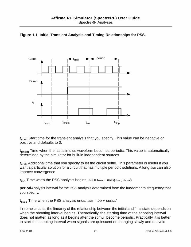
Affirma RF Simulator (SpectreRF) User GuideSpectreRF Analyses
Figure 1-1 Initial Transient Analysis and Timing Relationships for PSS.
tstart Start time for the transient analysis that you specify. This value can be negative orpositive and defaults to 0.
tonset Time when the last stimulus waveform becomes periodic. This value is automaticallydetermined by the simulator for built-in independent sources.
tstab Additional time that you specify to let the circuit settle. This parameter is useful if youwant a particular solution for a circuit that has multiple periodic solutions. A long tstab can alsoimprove convergence.
tinit Time when the PSS analysis begins. tinit = tstab + max(tstart, tonset)
period Analysis interval for the PSS analysis determined from the fundamental frequency thatyou specify.
tstop Time when the PSS analysis ends. tstop = tinit + period
In some circuits, the linearity of the relationship between the initial and final state depends onwhen the shooting interval begins. Theoretically, the starting time of the shooting intervaldoes not matter, as long as it begins after the stimuli become periodic. Practically, it is betterto start the shooting interval when signals are quiescent or changing slowly and to avoid
Clock
Reset
Q
tstart tonset tinit tstop
tstab period
April 2001 28 Product Version 4.4.6
Affirma RF Simulator (SpectreRF) User GuideSpectreRF Analyses
starting times when the circuit displays strongly nonlinear behavior. Choosing a poor startingtime slows the analysis.
The accuracy of results depends only on the accuracy parameters you set, not on the numberof harmonics you request. Except for a few new parameters, like steadyratio and maxacfreq,all PSS parameters work exactly as they work in transient analysis.
The steadyratio parameter specifies the maximum allowed mismatch between node voltagesor current branches from the beginning of the steady-state period to its end. The steadyratiovalue is multiplied by the lteratio and reltol parameter values to determine the convergencecriterion. You can follow the progress of the steady-state iterations because the relativeconvergence norm is printed along with the actual mismatch value at the end of eachiteration. The iterations continue until the convergence norm value is one.
The maxacfreq parameter automatically adjusts maxstep to reduce errors in subsequentperiodic small-signal analyses. By default, maxacfreq is four times the frequency of thelargest harmonic you request, but it is never less than 40 times the fundamental.
Periodic Distortion Analysis (Pdisto)
Pdisto models intermodulation distortion resulting from multiple moderately sized signals. Amoderately sized signal is one that has a few harmonics that contribute significantly to theoutput. You might use Pdisto, for example, to measure how well an amplifier avoidsmagnification of unwanted frequencies.
If you treat one of the input signals as a small signal, a signal whose harmonics do notcontribute significantly to the output, you can also model intermodulation distortion efficientlywith PAC, but Pdisto has the following advantages that make it the analysis of choice for somesituations:
With Pdisto, you can measure the harmonic distortion and frequency translation effectscreated by multiple moderate-signal inputs, including all third order products. Thesemeasurements are impossible using PAC because PAC does not model the effects ofsmall-signal harmonics.
With Pdisto, you can measure the effects of multiple moderate signals. With PAC, you arerestricted to modeling the effects of a single small signal on a fundamental you computeusing PSS. Pdisto lets you model all moderate-signal inputs, including sums of sinusoidsthat are not periodic.
To see the difference between the information available with Pdisto and PAC, compare howthe two approaches determine the output signals produced by input signals at 900MHz and905MHz. The discussion below assumes you are interested in data only for fundamentals andtheir first harmonics.
April 2001 29 Product Version 4.4.6
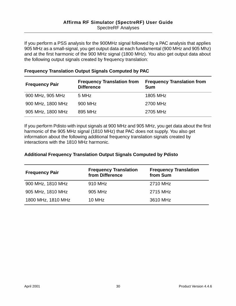
Affirma RF Simulator (SpectreRF) User GuideSpectreRF Analyses
If you perform a PSS analysis for the 900MHz signal followed by a PAC analysis that applies905 MHz as a small-signal, you get output data at each fundamental (900 MHz and 905 Mhz)and at the first harmonic of the 900 MHz signal (1800 MHz). You also get output data aboutthe following output signals created by frequency translation:
If you perform Pdisto with input signals at 900 MHz and 905 MHz, you get data about the firstharmonic of the 905 MHz signal (1810 MHz) that PAC does not supply. You also getinformation about the following additional frequency translation signals created byinteractions with the 1810 MHz harmonic.
Additional Frequency Translation Output Signals Computed by Pdisto
Frequency Translation Output Signals Computed by PAC
Frequency Pair Frequency Translation fromDifference
Frequency Translation fromSum
900 MHz, 905 MHz 5 MHz 1805 MHz
900 MHz, 1800 MHz 900 MHz 2700 MHz
905 MHz, 1800 MHz 895 MHz 2705 MHz
Frequency Pair Frequency Translationfrom Difference
Frequency Translationfrom Sum
900 MHz, 1810 MHz 910 MHz 2710 MHz
905 MHz, 1810 MHz 905 MHz 2715 MHz
1800 MHz, 1810 MHz 10 MHz 3610 MHz
April 2001 30 Product Version 4.4.6
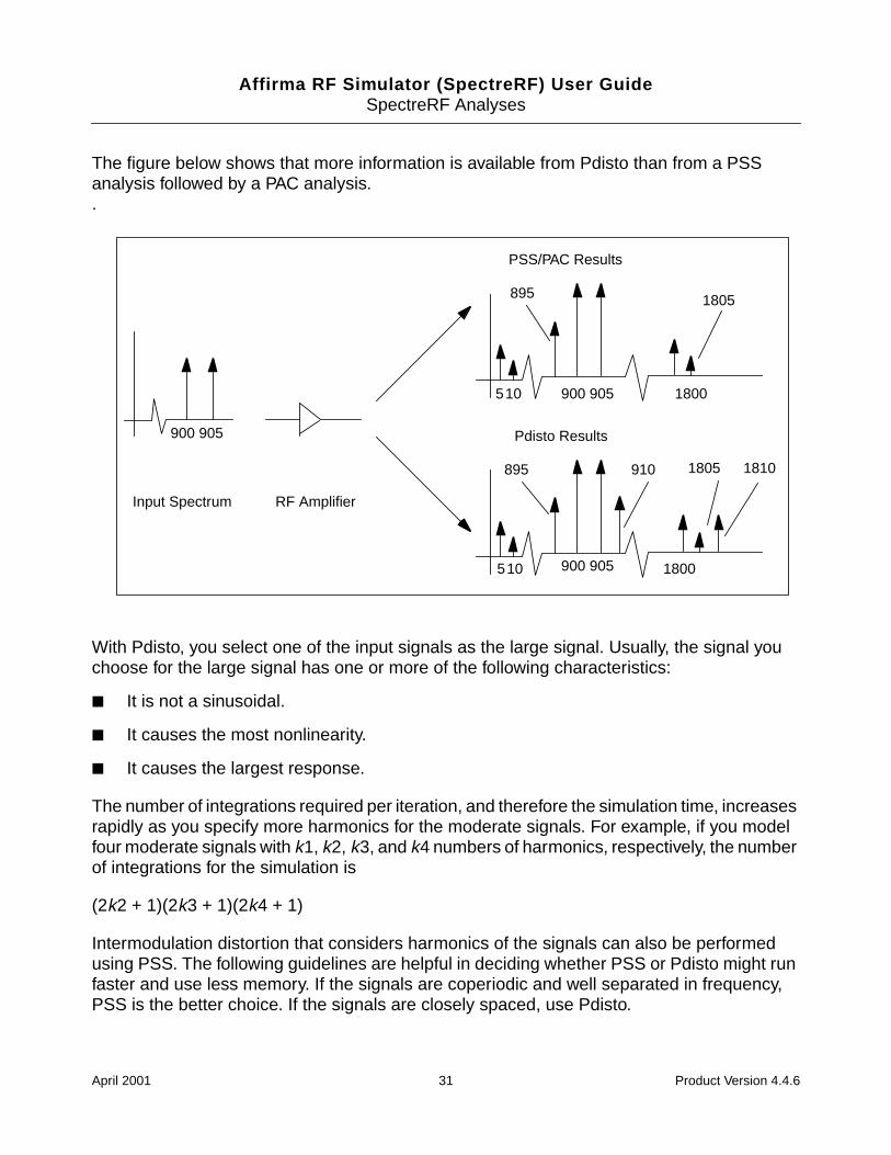
Affirma RF Simulator (SpectreRF) User GuideSpectreRF Analyses
The figure below shows that more information is available from Pdisto than from a PSSanalysis followed by a PAC analysis..
With Pdisto, you select one of the input signals as the large signal. Usually, the signal youchoose for the large signal has one or more of the following characteristics:
It is not a sinusoidal.
It causes the most nonlinearity.
It causes the largest response.
The number of integrations required per iteration, and therefore the simulation time, increasesrapidly as you specify more harmonics for the moderate signals. For example, if you modelfour moderate signals with k1, k2, k3, and k4 numbers of harmonics, respectively, the numberof integrations for the simulation is
(2k2 + 1)(2k3 + 1)(2k4 + 1)
Intermodulation distortion that considers harmonics of the signals can also be performedusing PSS. The following guidelines are helpful in deciding whether PSS or Pdisto might runfaster and use less memory. If the signals are coperiodic and well separated in frequency,PSS is the better choice. If the signals are closely spaced, use Pdisto.
510
510
900 905
900 905
1800
1800
895
895 1810910
1805
1805
900 905
Input Spectrum RF Amplifier
PSS/PAC Results
Pdisto Results
April 2001 31 Product Version 4.4.6
Affirma RF Simulator (SpectreRF) User GuideSpectreRF Analyses
Periodic AC Analysis
The Periodic AC (PAC) analysis computes transfer functions for circuits that exhibit frequencytranslation. Such circuits include mixers, switched-capacitor filters, samplers, phase-lockedloops, sample-and-holds, and similar circuits. A PAC analysis cannot be used alone. It mustfollow a PSS analysis. However, any number of periodic small-signal analyses can follow aPSS analysis.
When you apply a small sinusoid to a linear time-invariant circuit, the steady-state responseis a sinusoid at the same frequency. However, when you apply a small sinusoid to a linearcircuit that is periodically time-varying, the circuit responds with sinusoids at manyfrequencies, as is shown in Figure 1-2 on page 33.
Because PAC is a small-signal analysis, the magnitude and phase of each tone computed byPAC is linearly related to the magnitude and phase of the input signal. PAC computes a seriesof transfer functions, one for each frequency. These transfer functions are unique becausethe input and output frequencies are offset by the harmonics of the LO. The SpectreRFsimulation labels the transfer functions with the offsets from the input signal in multiples of theLO fundamental frequency. These same labels identify the corresponding sidebands of theoutput signals. The labels are used as follows:
For circuits in which the input and output are at the same frequency, such as switched-capacitor filters, the transfer function or sideband is labeled 0.
For down-conversion mixers, the transfer function or sideband is labeled -1 because theoutput frequency is offset from the input frequency by -1 times the LO frequency.
For up-conversion mixers, the transfer function or sideband is labeled +1.
For samplers, sidebands far from zero might be used.
In Figure 1-2 on page 33, all transfer functions from -3 to +3 are computed. As shown in thefigure, the input signal is replicated and translated by each harmonic of the LO. In down-conversion mixers, the -1 sideband usually represents the IF output.
April 2001 32 Product Version 4.4.6
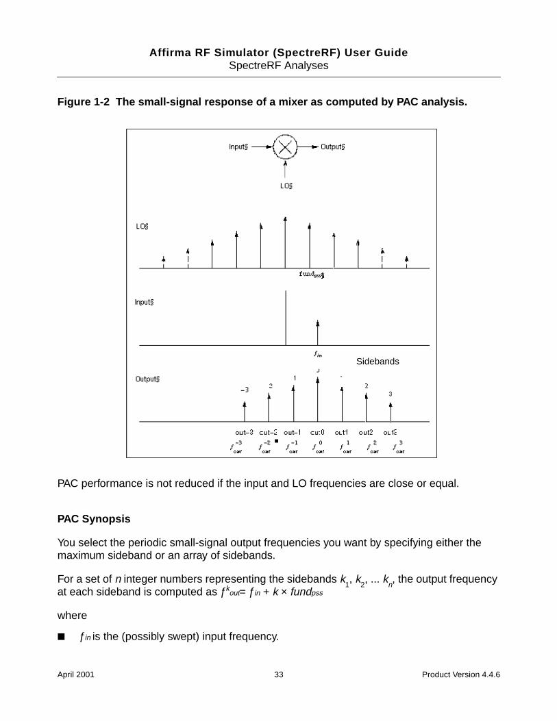
Affirma RF Simulator (SpectreRF) User GuideSpectreRF Analyses
Figure 1-2 The small-signal response of a mixer as computed by PAC analysis.
PAC performance is not reduced if the input and LO frequencies are close or equal.
PAC Synopsis
You select the periodic small-signal output frequencies you want by specifying either themaximum sideband or an array of sidebands.
For a set of n integer numbers representing the sidebands k1, k
2, ... k
n, the output frequency
at each sideband is computed as ƒkout= ƒin + k × fundpss
where
ƒin is the (possibly swept) input frequency.
Sidebands
April 2001 33 Product Version 4.4.6
Affirma RF Simulator (SpectreRF) User GuideSpectreRF Analyses
fundpss is the fundamental frequency used in the corresponding PSS analysis.
If you specify the maximum sideband value as kmax, all 2 × kmax + 1 sidebands from -kmax to+kmax are generated.
Intermodulation Distortion Computation
You can measure the intermodulation distortion of amplifiers and mixers with PAC. You canalso measure intermodulation distortion with Pdisto by applying two large, closely spacedtones to the input and then measuring the third-order intermodulation products. The PSS/PAC approach is slightly different. You apply only one large tone in the PSS analysis. PSS istherefore faster than Pdisto. Once PSS computes the circuit response to one large tone, thenPAC applies the second tone close to the first. If you consider the small input signal to be onesideband of the large input signal, then the response at the other sideband is the third-orderintermodulation distortion, as shown in Figure 1-3 on page 35.
In this figure, VL1 is the fundamental of the response due to the large input tone. VS1 is thefundamental of the response due to the small input tone and is the upper sideband of VL1.VS3 is the lower sideband of VL1 (in this case, it is the -2 sideband of the response due to thesmall tone). VS3 represents the intermodulation distortion. In the lower figure, all of the signalsare mapped into positive frequencies, which is the most common way of viewing such results.
April 2001 34 Product Version 4.4.6
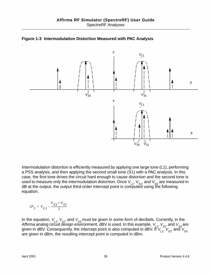
Affirma RF Simulator (SpectreRF) User GuideSpectreRF Analyses
Figure 1-3 Intermodulation Distortion Measured with PAC Analysis.
Intermodulation distortion is efficiently measured by applying one large tone (L1), performinga PSS analysis, and then applying the second small tone (S1) with a PAC analysis. In thiscase, the first tone drives the circuit hard enough to cause distortion and the second tone isused to measure only the intermodulation distortion. Once V
L1, V
S1, and V
S3are measured in
dB at the output, the output third-order intercept point is computed using the followingequation.
In the equation, VL1
, VS1
, and VS3
must be given in some form of decibels. Currently, in theAffirma analog circuit design environment, dBV is used. In this example, V
L1, V
S1, and V
S3are
given in dBV. Consequently, the intercept point is also computed in dBV. If VL1
, VS1
, and VS3
are given in dBm, the resulting intercept point is computed in dBm.
VL1
VS3 VS1
VS3 VS1
VL1
Y
Y
X
X
IP3 VL1
VS3 VS1+
2---------------------------–=
April 2001 35 Product Version 4.4.6
Affirma RF Simulator (SpectreRF) User GuideSpectreRF Analyses
The intermodulation distortion of a mixer is measured in a similar manner, except that thePSS analysis must include both the LO and one large tone. For an example of measuring theintermodulation distortion of a mixer, see Chapter 4, “Simulating Mixers with SpectreRFsimulation.”
If you must measure intermodulation distortion using two large tones to compare againstbench measurements, you can run PSS analysis with two large tones. However, do so onlywhen absolutely necessary. At other times, use the quicker PSS/PAC approach.
Periodic S-Parameter Analysis
The Periodic S-Parameter (PSP) analysis is used to compute scattering and noiseparameters for n-port circuits that exhibit frequency translation. Such circuits include mixers,switched-capacitor filters, samplers, phase-locked loops, and other similar circuits.
PSP is a small-signal analysis similar to SP analysis, except, as for PAC and PXF analyses,the circuit is first linearized about a periodically varying operating point as opposed to asimple DC operating point. Linearizing about a periodically time-varying operating pointallows the computation of S-parameters between circuit ports that convert signals from onefrequency band to another.
PSP analysis also calculates noise parameters in frequency-converting circuits. PSPcomputes noise figure (both single-sideband and double-sideband), input referred noise,equivalent noise parameters, and noise correlation matrices. The noise features of PSPanalysis, as for Pnoise analysis but unlike SP analysis, include noise folding effects due tothe periodically time-varying nature of the circuit.
Computing the n-port S-parameters and noise parameters of a periodically varying circuit isa two step process.
First, the small stimulus is ignored and the periodic steady-state response of the circuitto possibly large periodic stimulus is computed using PSS analysis.
As a normal part of the PSS analysis, the periodically time-varying representation of thecircuit is computed and saved for later use.
Then, using the PSP analysis, small-signal excitations are applied to compute the n-portS-parameters and noise parameters.
A PSP analysis cannot be used alone, it must follow a PSS analysis. However, anynumber of periodic small-signal analyses such as PAC, PSP, PXF, and Pnoise, can followa single PSS analysis.
Unlike other analyses in Spectre, the PSP analysis can sweep only frequency.
April 2001 36 Product Version 4.4.6
Affirma RF Simulator (SpectreRF) User GuideSpectreRF Analyses
PSP Synopsis
For a PSP analysis, you need to specify the port and port harmonic relations. Select the portsof interest by setting the port parameter. Set the periodic small-signal output frequencies ofinterest by setting the portharmsvec or the harmsvec parameters.
For a given set of n integer numbers representing the harmonics K1, K2, ... Kn, the scatteringparameters at each port are computed at the frequencies f(scattered)= f(rel) + Ki *fund(pss), where f(rel) represents the relative frequency of a signal incident on a port,f(scattered) represents the frequency to which the relevant scattering parameter representsthe conversion, and fund(pss) represents the fundamental frequency used in thecorresponding PSS analysis.
Thus, when analyzing a down-converting mixer, with signal in the upper sideband, andsweeping the RF input frequency, the most relevant harmonic for RF input is Ki= 1 and for IFoutput Ki= 0. Hence we can associate K2=0 with the IF port and K1=1 with the RF port. S21will represent the transmission of signal from the RF to IF, and S11 the reflection of signalback to the RF port. If the signal was in the lower sideband, then a choice of K1=-1 would bemore appropriate.
You can use either the portharmsvec or the harmsvec parameters to specify the harmonicsof interest. If you give portharmsvec, the harmonics must be in one-to-one correspondencewith the ports, with each harmonic associated with a single port. If you specify harmonics withthe optional harmsvec parameter, then all possible frequency-translating scatteringparameters associated with the specified harmonics are computed.
For PSP analysis, the frequencies of the input and of the response are usually different (thisis an important way in which PSP differs from SP). Because the PSP computation involvesinputs and outputs at frequencies that are relative to multiple harmonics, the freqaxis andsweeptype parameters behave somewhat differently in PSP than they do in PAC and PXF.
The sweeptype parameter controls the way the frequencies are swept in PSP analysis.Specifying relative sweep, sweeps relative to the analysis harmonics (not the PSSfundamental). Specifying absolute sweep, sweeps the absolute input source frequency. Forexample, with a PSS fundamental of 100MHz, the portharmsvec set to [9 1] to examine adown-converting mixer, sweeptype=relative, and a sweep range of f(rel)=0->50MHz, thenS21 would represent the strength of signal transmitted from the input port in the range 900->950MHz to the output port at frequencies 100->150MHz.
Using sweeptype=absolute and sweeping the frequency from 900->950MHz wouldcalculate the same quantities, since f(abs)=900->950MHz, and f(rel) = f(abs) - K1 *fund(pss) = 0->50MHz, because K1=9 and fund(pss) = 100MHz.
In a PSP analysis, it is not usually necessary to sweep frequency over more than onefundamental PSS period.
April 2001 37 Product Version 4.4.6
Affirma RF Simulator (SpectreRF) User GuideSpectreRF Analyses
The freqaxis parameter is used to specify whether the results should be output versus thescattered frequency at the input port(in), the scattered frequency at the output port(out), orthe absolute value of the frequency swept at the input port(absin).
Unlike in PAC, PXF, and Pnoise analyses, increasing the number of requested ports andharmonics increases the simulation time substantially.
To insure accurate results in PSP analysis, you should set the maxacfreq parameter for thecorresponding PSS analysis to guarantee that |maxf(scattered)| is less than themaxacfreq parameter value, otherwise the computed solution might be contaminated byaliasing effects.
PSP analysis computes noise figures, equivalent noise sources, and noise parameters. Thenoise computation, which is skipped only when the donoise parameter is set to no, requiresadditional simulation time.
If
No = total output noise at frequency f
Ns = noise at the output due to the input probe (the source)
Nsi = noise at the output due to the image harmonic at the source
Nso = noise at the output due to harmonics other than input at the source
Nl = noise at the output due to the output probe (the load)
IRN = input referred noise
G = gain of the circuit
F = noise factor (single side band)
NF = noise figure (single side band)
Fdsb = double sideband noise factor
NFdsb = double sideband noise figure
Fieee = IEEE single sideband noise factor
NFieee = IEEE single sideband noise figure
then,
April 2001 38 Product Version 4.4.6
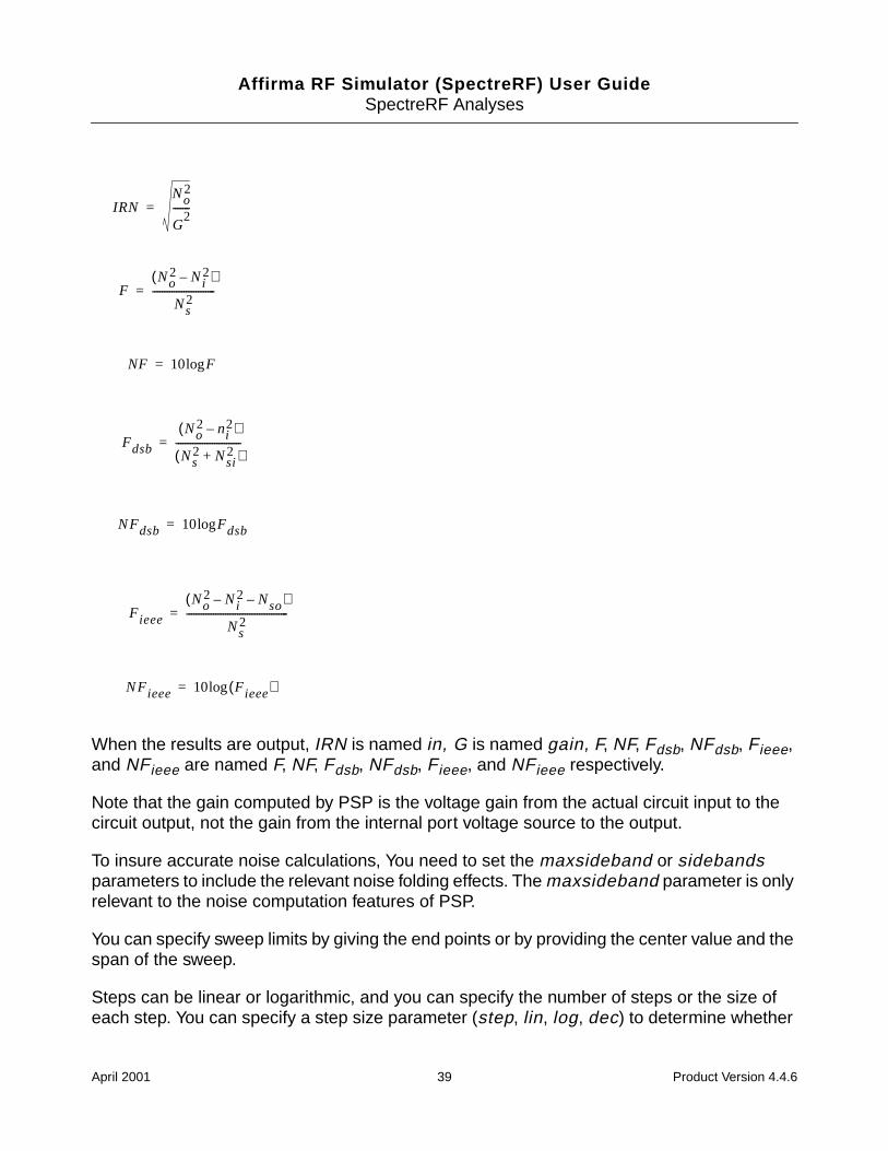
Affirma RF Simulator (SpectreRF) User GuideSpectreRF Analyses
When the results are output, IRN is named in, G is named gain, F, NF, Fdsb, NFdsb, Fieee,and NFieee are named F, NF, Fdsb, NFdsb, Fieee, and NFieee respectively.
Note that the gain computed by PSP is the voltage gain from the actual circuit input to thecircuit output, not the gain from the internal port voltage source to the output.
To insure accurate noise calculations, You need to set the maxsideband or sidebandsparameters to include the relevant noise folding effects. The maxsideband parameter is onlyrelevant to the noise computation features of PSP.
You can specify sweep limits by giving the end points or by providing the center value and thespan of the sweep.
Steps can be linear or logarithmic, and you can specify the number of steps or the size ofeach step. You can specify a step size parameter (step, lin, log, dec) to determine whether
IRNNo
2
G2
-------=
FNo
2 Ni2–( )
Ns2
--------------------------=
NF 10 Flog=
Fdsb
No2 ni
2–( )
Ns2 Nsi
2+( )---------------------------=
NFdsb 10 Fdsblog=
Fieee
No2 Ni
2– Nso–( )
Ns2
------------------------------------------=
NFieee 10 Fieee( )log=
April 2001 39 Product Version 4.4.6
Affirma RF Simulator (SpectreRF) User GuideSpectreRF Analyses
the sweep is linear or logarithmic. If you do not give a step size parameter, the sweep is linearwhen the ratio of stop to start values is less than 10:1, and logarithmic when this ratio is equalto or greater than 10:1.
Alternatively, you may specify particular values for the sweep parameter using the valuesparameter. If you give both a specific set of values and a set specified using a sweep range,the two sets are merged and collated before being used. All frequencies are in Hertz.
Periodic Transfer Function Analysis
Whereas a conventional AC analysis computes the response from a single stimulus to everynode in the circuit, a conventional transfer function (XF) analysis computes the transferfunction from every source in the circuit to a single output. The difference between PAC andPXF analysis is similar. The PXF analysis computes the transfer functions from any sourceat any frequency to a single output at a single frequency. Like PAC analysis, PXF analysismodels frequency conversion effects. This is illustrated in Figure 1-4 on page 41. PXFcomputes such useful quantities as conversion efficiency, image and sideband rejection, andLO feed through and power supply rejection.
The output is sensitive to signals at many frequencies at the input of the mixer. The inputsignals are replicated and translated by each harmonic of the LO. The signals shown in thefigure are those that end up at the output frequency.
April 2001 40 Product Version 4.4.6
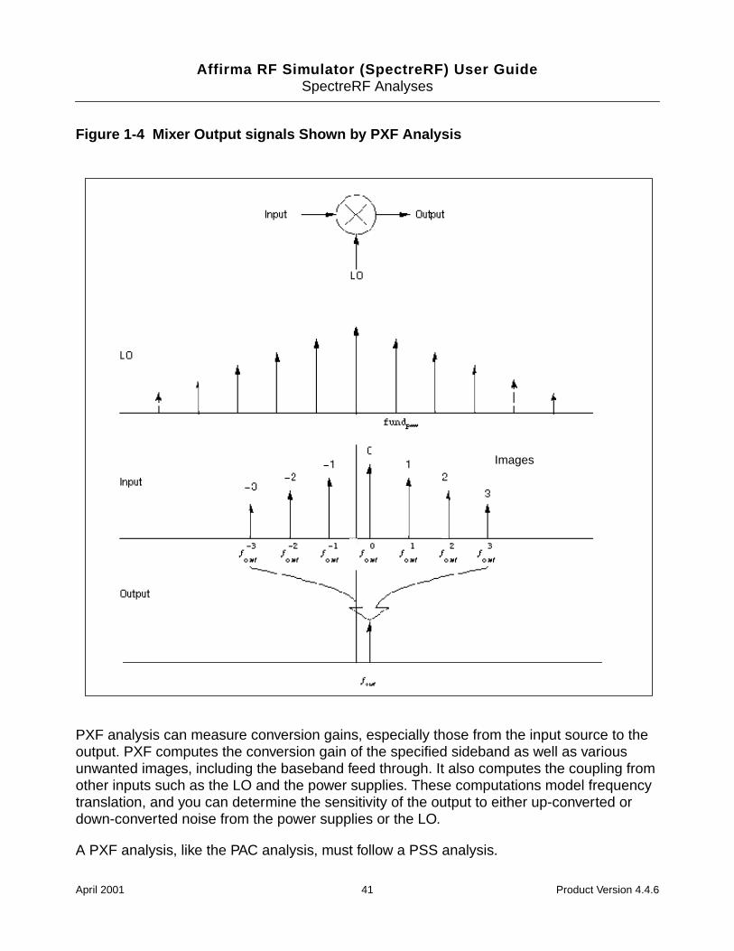
Affirma RF Simulator (SpectreRF) User GuideSpectreRF Analyses
Figure 1-4 Mixer Output signals Shown by PXF Analysis
PXF analysis can measure conversion gains, especially those from the input source to theoutput. PXF computes the conversion gain of the specified sideband as well as variousunwanted images, including the baseband feed through. It also computes the coupling fromother inputs such as the LO and the power supplies. These computations model frequencytranslation, and you can determine the sensitivity of the output to either up-converted ordown-converted noise from the power supplies or the LO.
A PXF analysis, like the PAC analysis, must follow a PSS analysis.
Images
April 2001 41 Product Version 4.4.6
Affirma RF Simulator (SpectreRF) User GuideSpectreRF Analyses
PXF Synopsis
The output variable you measure can be voltage or current, and the variable frequency is notlimited by the period of the large-periodic solution. When you sweep a selected outputfrequency, you can select the periodic small-signal input frequencies by specifying either themaximum sideband or an array of sidebands.
For a set of n integer numbers representing the sidebands k1, k
2, …k
n, the input signal
frequency at each sideband is computed as ƒkin= ƒout + k × fundpss
where
ƒout represents the (possibly swept) output signal frequency
fundpss represents the fundamental frequency used in the corresponding PSS analysis
When you analyze a down-converting mixer and sweep the IF output frequency, k= +1 for theRF input represents the first upper sideband, and k = -1 for the RF input represents the firstlower sideband. If you specify kmax as the maximum sideband value, you select all 2 × kmax +1 sidebands from -kmax to +kmax. The number of sidebands you request does not affectaccuracy, so request only sidebands that you want to see.
You can specify the output with a pair of nodes or a probe component. Any component withtwo or more terminals can be a voltage probe. Any component that naturally computescurrent as an internal variable, such as a voltage source, can be a current probe. In theAffirma analog circuit design environment, you set probes on the Choosing Analysis formwhen you specify input or output sources, and also when you specify positive or negativeoutput nodes.
The stimuli parameter on the PXF Options form specifies the inputs for the transfer functions.You select from the following choices:
stimuli = sources specifies that the sources present in the circuit are used. The xfmagcomponent parameter provided by the sources can adjust the computed gain tocompensate for gains or losses in a test fixture.
stimuli = nodes_and_terminals specifies that all possible transfer functions arecomputed. Use this option when you cannot anticipate which transfer functions you mightneed to examine.
Transfer functions for nodes are computed assuming that a unit magnitude flow (current)source is connected from the node to ground. Transfer functions for terminals are computedassuming that a unit magnitude value (voltage) source is connected in series with theterminal. By default, PXF computes the transfer functions from a small set of terminals.
April 2001 42 Product Version 4.4.6
Affirma RF Simulator (SpectreRF) User GuideSpectreRF Analyses
Periodic Noise Analysis
The Periodic Noise analysis (Pnoise) is similar to conventional noise analysis except that itmodels frequency conversion effects. It can compute the phase noise of oscillators as well asthe noise behavior of mixers, switched-capacitor filters, chopper-stabilized amplifiers, andother similar circuits.
PSS analysis linearizes the circuit about the periodic operating point. The periodically time-varying qualities of the linearized circuit create the frequency conversion. Then the effect ofa periodically time-varying bias point on component-generated noise is simulated by Pnoise.
Initially, PSS computes the response to a large periodic signal such as a clock or a LO. Theseresults are labeled LO and shown in Figure 1-5 on page 44. The subsequent Pnoise analysiscomputes the resulting noise performance.
In periodic systems, there are two effects that act to translate noise in frequency. First, fornoise sources that are bias dependent, such as shot noise sources, the time-varyingoperating point modulates the noise sources. Second, the transfer function from the noisesource to the output is also periodically time-varying and modulates the noise sourcecontribution to the output.
April 2001 43 Product Version 4.4.6
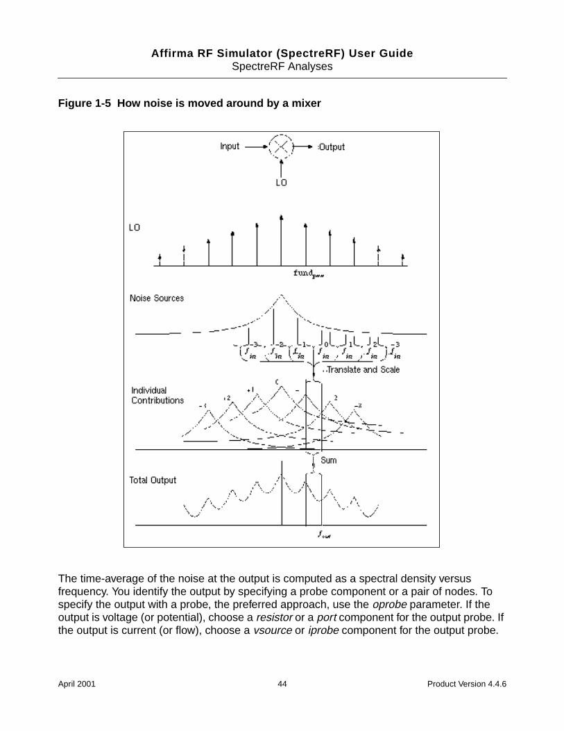
Affirma RF Simulator (SpectreRF) User GuideSpectreRF Analyses
Figure 1-5 How noise is moved around by a mixer
The time-average of the noise at the output is computed as a spectral density versusfrequency. You identify the output by specifying a probe component or a pair of nodes. Tospecify the output with a probe, the preferred approach, use the oprobe parameter. If theoutput is voltage (or potential), choose a resistor or a port component for the output probe. Ifthe output is current (or flow), choose a vsource or iprobe component for the output probe.
April 2001 44 Product Version 4.4.6

Affirma RF Simulator (SpectreRF) User GuideSpectreRF Analyses
The reference sideband (refsideband) specifies which conversion gain is used to compute theinput-referred noise, the noise factor, and the noise figure. The reference sideband satisfiesthe following equation.
Use refsideband=0 when the input and output are at the same frequency, such as withamplifiers and filters. When refsideband does not equal 0, the single side band noise figureis computed.
The noise analysis computes the total noise at the output, which includes contributions fromthe input source and the output load. The output noise that is attributable to each noise sourceis specified in the results. If the input source is identified, the input-referred noise is alsocomputed, and this includes the noise from the input source itself. Finally, if the input sourceis identified and is also noisy, the noise factor and noise figure are computed.
Thus, if
No = Total output noise
Ns = Noise at the output due to the input source
Nl = Noise at the output due to the load
IRN = Input referred noise
G = Voltage gain of input node voltage to output node voltage
F = Noise factor
NF = Noise figure
then
f input( ) f output( ) refsideband fund pss( )×+=
IRN No2 G2§=
FNo
2 Nl2–
Ns2
---------------------=
NF 10 F( )log=
April 2001 45 Product Version 4.4.6
Affirma RF Simulator (SpectreRF) User GuideSpectreRF Analyses
Pnoise Synopsis
Noise can mix with each harmonic of the periodic drive signal from the PSS analysis andappear at the output frequency. However, Pnoise analysis models only noise that mixes witha set of harmonics that you normally specify with the maxsideband parameter, but which youmight specify with the sidebands parameter in special circumstances. If Ki representssideband i, then
The maxsideband parameter specifies the maximum |Ki| included in the Pnoise calculation.Therefore, Pnoise ignores noise at frequencies less than f(out) – maxsideband fund(pss) andgreater than f(out) + maxsideband fund(pss). If you specify sidebands with the sidebandsparameter, then Pnoise includes only the specified sidebands in the calculation. When youspecify sidebands parameter values, be careful not to omit any sidebands that mightcontribute significant output noise.
In the Affirma analog circuit design environment, you specify the maxsideband parameterwith the Maximum sideband specification in the Choosing Analyses form. You specify thesidebands parameter in the Array of Sidebands type-in field.
Increasing the number of harmonics computed by Pnoise improves simulation accuracybecause it increases the number of harmonics used to compute the effects of noise folding.Noise folding is noise mixing with the harmonics into the frequency range of interest.
Noise Figure
When you use Pnoise analysis to compute the noise factor or noise figure of a circuit, and theload generates noise, specify the output with the oprobe parameter rather than using a pairof nodes. Using the oprobe parameter explicitly specifies the load as the output probe. Thisis preferable because it excludes the noise of the load from the calculation of the noise figure.
As an alternative, you can specify the output with a pair of nodes and make the loadcomponent a noiseless resistor. Results with this approach are similar to those computed ifyou specify a resistor or a port as the output probe (load). The only difference is that thenoiseless resistor is considered noiseless for other noise calculations, such as total outputnoise and input-referred noise, and the resistor is noiseless at all frequencies. When youspecify a conventional resistor or port for the load, its noise is subtracted from only the noisefactor and noise figure calculations, and only at the output frequency. Consequently, noisefrom load frequencies other than the output frequency can appear at the output frequency ifthe circuit has a nonlinear output impedance.
f NoiseSource( ) f out( ) Ki fund pss( )+=
April 2001 46 Product Version 4.4.6
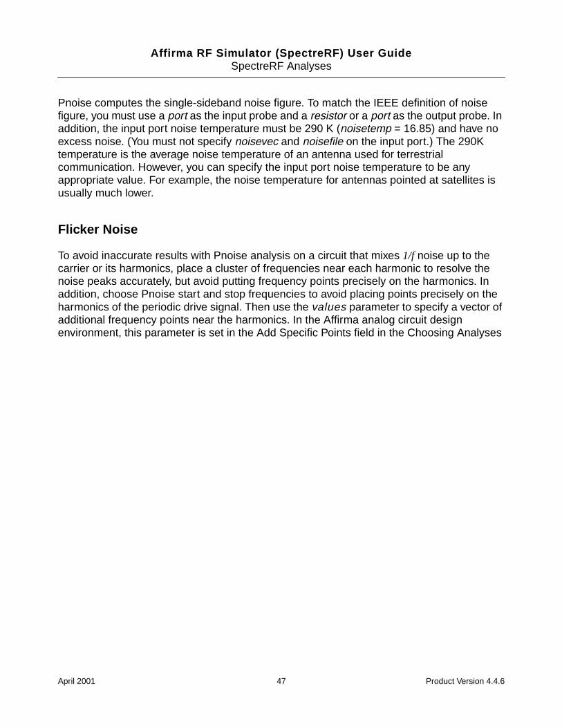
Affirma RF Simulator (SpectreRF) User GuideSpectreRF Analyses
Pnoise computes the single-sideband noise figure. To match the IEEE definition of noisefigure, you must use a port as the input probe and a resistor or a port as the output probe. Inaddition, the input port noise temperature must be 290 K (noisetemp = 16.85) and have noexcess noise. (You must not specify noisevec and noisefile on the input port.) The 290Ktemperature is the average noise temperature of an antenna used for terrestrialcommunication. However, you can specify the input port noise temperature to be anyappropriate value. For example, the noise temperature for antennas pointed at satellites isusually much lower.
Flicker Noise
To avoid inaccurate results with Pnoise analysis on a circuit that mixes 1/f noise up to thecarrier or its harmonics, place a cluster of frequencies near each harmonic to resolve thenoise peaks accurately, but avoid putting frequency points precisely on the harmonics. Inaddition, choose Pnoise start and stop frequencies to avoid placing points precisely on theharmonics of the periodic drive signal. Then use the values parameter to specify a vector ofadditional frequency points near the harmonics. In the Affirma analog circuit designenvironment, this parameter is set in the Add Specific Points field in the Choosing Analyses
April 2001 47 Product Version 4.4.6
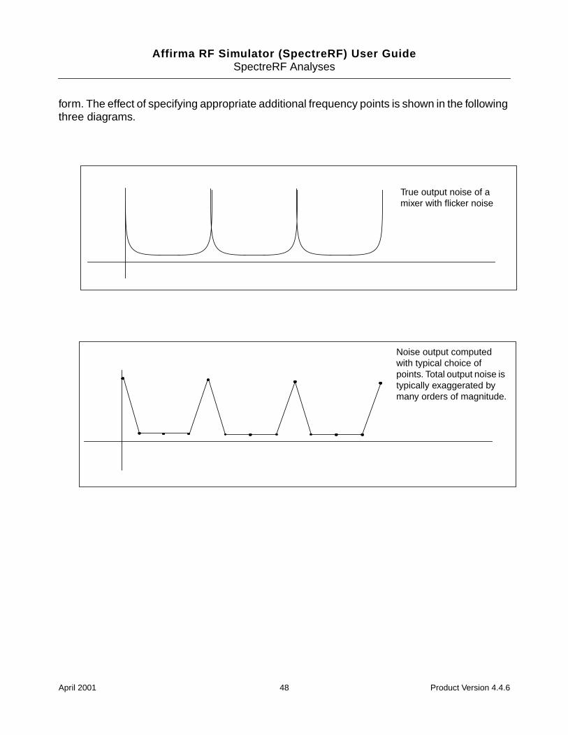
Affirma RF Simulator (SpectreRF) User GuideSpectreRF Analyses
form. The effect of specifying appropriate additional frequency points is shown in the followingthree diagrams.
True output noise of amixer with flicker noise
Noise output computedwith typical choice ofpoints. Total output noise istypically exaggerated bymany orders of magnitude.
April 2001 48 Product Version 4.4.6
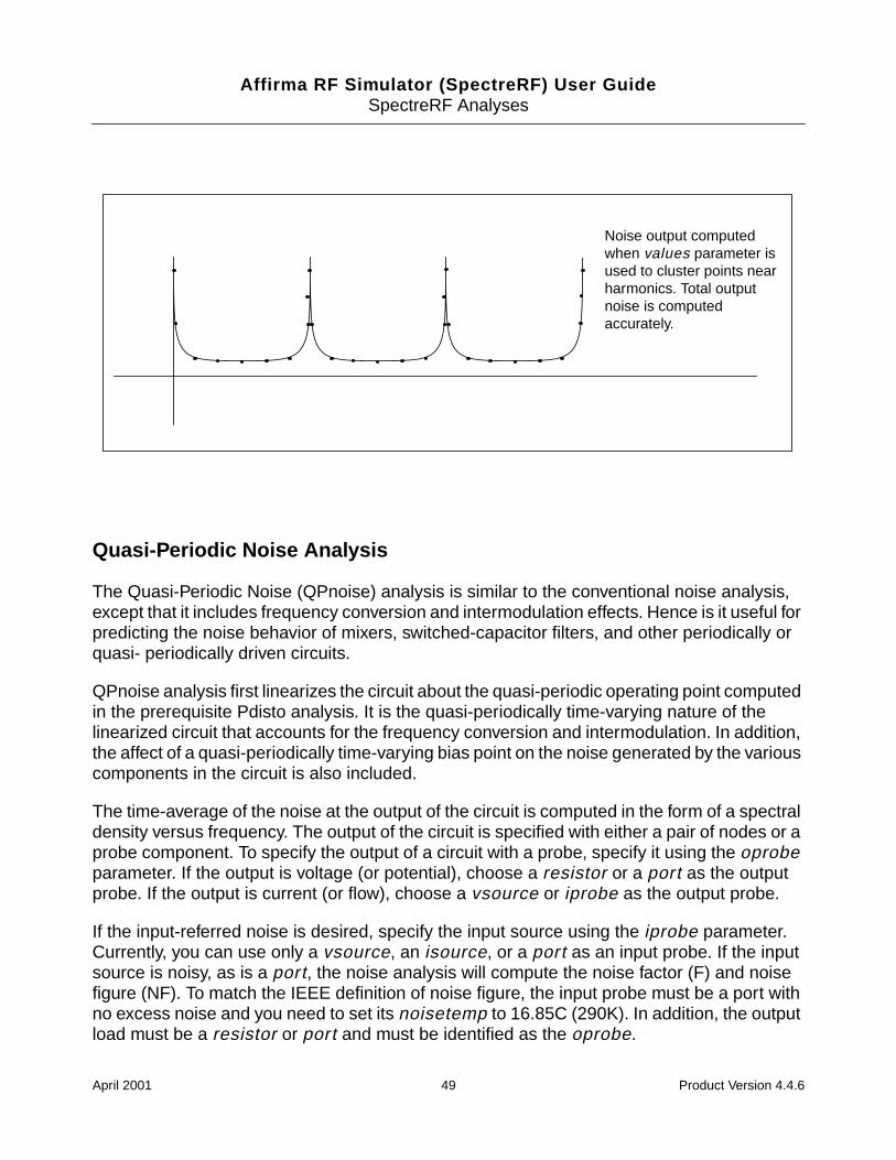
Affirma RF Simulator (SpectreRF) User GuideSpectreRF Analyses
Quasi-Periodic Noise Analysis
The Quasi-Periodic Noise (QPnoise) analysis is similar to the conventional noise analysis,except that it includes frequency conversion and intermodulation effects. Hence is it useful forpredicting the noise behavior of mixers, switched-capacitor filters, and other periodically orquasi- periodically driven circuits.
QPnoise analysis first linearizes the circuit about the quasi-periodic operating point computedin the prerequisite Pdisto analysis. It is the quasi-periodically time-varying nature of thelinearized circuit that accounts for the frequency conversion and intermodulation. In addition,the affect of a quasi-periodically time-varying bias point on the noise generated by the variouscomponents in the circuit is also included.
The time-average of the noise at the output of the circuit is computed in the form of a spectraldensity versus frequency. The output of the circuit is specified with either a pair of nodes or aprobe component. To specify the output of a circuit with a probe, specify it using the oprobeparameter. If the output is voltage (or potential), choose a resistor or a port as the outputprobe. If the output is current (or flow), choose a vsource or iprobe as the output probe.
If the input-referred noise is desired, specify the input source using the iprobe parameter.Currently, you can use only a vsource, an isource, or a port as an input probe. If the inputsource is noisy, as is a port, the noise analysis will compute the noise factor (F) and noisefigure (NF). To match the IEEE definition of noise figure, the input probe must be a port withno excess noise and you need to set its noisetemp to 16.85C (290K). In addition, the outputload must be a resistor or port and must be identified as the oprobe.
Noise output computedwhen values parameter isused to cluster points nearharmonics. Total outputnoise is computedaccurately.
April 2001 49 Product Version 4.4.6
Affirma RF Simulator (SpectreRF) User GuideSpectreRF Analyses
The reference sideband (refsideband) specifies which conversion gain is used whencomputing input-referred noise, noise factor, and noise figure. The reference sidebandsatisfies:
|f(input)| = |f(out) + refsideband frequency shift|
The reference sideband option (refsidebandoption) specifies whether to consider the inputat the frequency or the input at the individual quasi-periodic sideband specified. Note thatdifferent sidebands might lead to the same frequency.
Sidebands are vectors in QPnoise analysis.
Assume you have one large tone and one moderate tone in a Pdisto analysis. A sidebandmight be [K1 K2]. It gives the frequency as follows
K1 * fund(large tone of Pdisto) + K2 * fund(moderate tone of Pdisto)
Use refsideband=[0 0 ...] when the input and output of the circuit are at the same frequency(such as with amplifiers and filters). When refsideband differs from the 0 vector, the singleside-band noise figure is computed.
The noise analysis always computes the total noise at the output, which includescontributions from the input source and the output load. The amount of the output noise thatis attributable to each noise source in the circuit is also computed and output individually. Ifthe input source is identified, the input-referred noise is computed, which includes the noisefrom the input source itself. Finally, if the input source is identified and is noisy, the noise factorand noise figure are computed.
Thus if
No = total output noise
Ns = noise at the output due to the input probe (the source)
Nl = noise at the output due to the output probe (the load)
IRN = input referred noise
G = gain of the circuit
F = noise factor
NF = noise figure
April 2001 50 Product Version 4.4.6
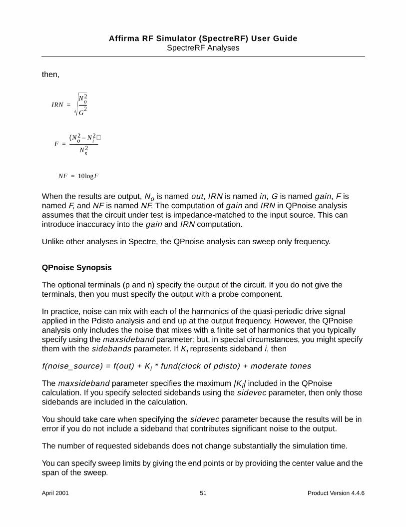
Affirma RF Simulator (SpectreRF) User GuideSpectreRF Analyses
then,
When the results are output, No is named out, IRN is named in, G is named gain, F isnamed F, and NF is named NF. The computation of gain and IRN in QPnoise analysisassumes that the circuit under test is impedance-matched to the input source. This canintroduce inaccuracy into the gain and IRN computation.
Unlike other analyses in Spectre, the QPnoise analysis can sweep only frequency.
QPnoise Synopsis
The optional terminals (p and n) specify the output of the circuit. If you do not give theterminals, then you must specify the output with a probe component.
In practice, noise can mix with each of the harmonics of the quasi-periodic drive signalapplied in the Pdisto analysis and end up at the output frequency. However, the QPnoiseanalysis only includes the noise that mixes with a finite set of harmonics that you typicallyspecify using the maxsideband parameter; but, in special circumstances, you might specifythem with the sidebands parameter. If Ki represents sideband i, then
f(noise_source) = f(out) + Ki * fund(clock of pdisto) + moderate tones
The maxsideband parameter specifies the maximum |Ki| included in the QPnoisecalculation. If you specify selected sidebands using the sidevec parameter, then only thosesidebands are included in the calculation.
You should take care when specifying the sidevec parameter because the results will be inerror if you do not include a sideband that contributes significant noise to the output.
The number of requested sidebands does not change substantially the simulation time.
You can specify sweep limits by giving the end points or by providing the center value and thespan of the sweep.
IRNNo
2
G2
-------=
FNo
2 Ni2–( )
Ns2
--------------------------=
NF 10 Flog=
April 2001 51 Product Version 4.4.6
Affirma RF Simulator (SpectreRF) User GuideSpectreRF Analyses
Steps can be linear or logarithmic, and you can specify the number of steps or the size ofeach step. You can specify a step size parameter (step, lin, log, dec) to determine whetherthe sweep is linear or logarithmic. If you do not give a step size parameter, the sweep is linearwhen the ratio of stop to start values is less than 10:1, and logarithmic when this ratio is equalto or greater than 10:1.
Alternatively, you may specify the particular values for the sweep parameter using the valuesparameter. If you give both a specific set of values and a set specified using a sweep range,the two sets are merged and collated before being used. All frequencies are in Hertz.
Envelope Following Analysis
RF circuit designers who simulate the modulation schemes of communications systems wantefficient and accurate prediction of the envelope transient response of RF circuits. Typically,these modulation schemes are difficult to simulate because they are clocked at a frequencywhose period is orders of magnitude smaller than the time interval of interest. Using classicaltransient simulation for these circuits is time-consuming, and new RF analyses, such as PSSand PDISTO, might not work directly because the modulation signal is sometimes stochasticand might be neither periodic nor quasi-periodic.
Envelope Following Analysis permits efficient simulation of these modulation schemes andreduces the simulation time without compromising accuracy. This analysis depends on theproperty that circuit behavior in a given high-frequency clock cycle is similar, but not identical,to the behavior of the preceding and following clock cycles. In particular, the “envelope” of thehigh-frequency clock can be followed by accurately computing the circuit behavior overoccasional cycles that accurately model the fast transient behavior. The slow-varyingmodulation is accurately followed by a piecewise polynomial. As a result, the spectrum of thecircuit response can be obtained by combining the piecewise polynomial and the integrationof the occasional clock cycles.
To compute the envelope response of a circuit, you specify the analysis clock name. Thesimulator automatically determines the clock period by examining all the sources with thespecified name. The envelope response is computed over the interval from Start to Stop. Ifthe interval you specify is not a multiple of the clock period, it is rounded off to the nearestmultiple before the Stop time. The initial condition is assumed to be the DC steady-statesolution unless you specify otherwise.
Envelope Following Analysis is most efficient for circuits whose modulation bandwidth isorders of magnitude lower than the clock frequency. This is typically the case, for example, incircuits whose clock is the only fast varying signal, and whose other input signals have aspectrum with a frequency range orders of magnitude lower than the clock frequency.
April 2001 52 Product Version 4.4.6
Affirma RF Simulator (SpectreRF) User GuideSpectreRF Analyses
In general, Envelope Following Analysis is not intended for circuits working with multiplefundamentals. However, like Periodic Steady-State (PSS) Analysis, you can use it for specificclasses of circuits that operate with multiple fundamentals.
You can, for example, use Envelope Following Analysis when the multiple fundamentals arecommensurate. In this situation, you use the greatest common denominator of allfundamental frequencies as the clock frequency. This is similar to computing the beatfrequency for PSS analysis. The analysis efficiency is also analogous to PSS analysis. Ateach integration of the clock period, many fast cycles might be required. The analysisefficiency depends on how many fast cycles are required for the beat period. Greaternumbers of fast cycles decrease the efficiency of the analysis.
Envelope Following analysis differs from PSS in that you can give the fundamentals the samename by using the clockname parameter, and the simulator then computes the beatfrequency automatically. With PSS analysis, in similar circumstances, you must either specifythe beat frequency or have it computed from fundamental tones that you specify in the UI.
There is a second situation when Envelope Following Analysis is useful for circuits withmultiple fundamentals. This is when the down conversion of two closely placed frequenciescan also generate a slow-varying modulation envelope whose frequency is orders ofmagnitude lower than the input frequencies. In this case, you can use Envelope FollowingAnalysis to trace out the modulation envelope by choosing either of the fast-varying signalsas the clock. However, you usually choose the signal that causes the most nonlinearity.
Envelope Following Analysis generates two types of output files: a voltage versus time (td)file, and an amplitude/phase versus time (fd) file for each of specified harmonic of the clockfundamental.
The td file contains time-domain real waveforms. They are similar to the waveformsgenerated by transient analysis. The difference between the analyses is that the integrationof a clock cycle occurs much less frequently with Envelope Following Analysis. Consequently,you usually see big gaps between integrated clock cycles.
The fd file contains time varying Fourier coefficients (complex) of circuit response at clockharmonics. The most interesting harmonic is probably the first one. The real and imaginaryparts of this harmonic are called the in-phase and quadrature components of the basebandsignal. Assume, for example, that you simulate a transmitter that is driven by a complexbaseband signal. For a phase-modulation scheme, you plot the phase of the time-varyingfundamental versus time to see the transmitted phase. To see the trajectory of the transmittedbaseband signal, plot the real versus the imaginary parts of the time-varying fundamental.The trajectory lets you visually check the error vector magnitude (EVM). To compute thetransmitted power spectral density about the carrier, compute the power spectral density ofthe time-varying fundamental. From the power spectral density, you can estimate AdjacentChannel Power Ratio (ACPR).
April 2001 53 Product Version 4.4.6

Affirma RF Simulator (SpectreRF) User GuideSpectreRF Analyses
The spectrum of each harmonic response is calculated from the Affirma analog circuit designenvironment. This is useful for applications such as ACPR calculation.
You can also use the fd result for applications such as constellation diagrams, by plottingamplitude versus phase.
April 2001 54 Product Version 4.4.6
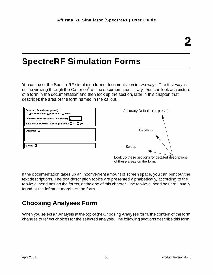
Affirma RF Simulator (SpectreRF) User Guide
2SpectreRF Simulation Forms
You can use the SpectreRF simulation forms documentation in two ways. The first way isonline viewing through the Cadence® online documentation library.. You can look at a pictureof a form in the documentation and then look up the section, later in this chapter, thatdescribes the area of the form named in the callout.
If the documentation takes up an inconvenient amount of screen space, you can print out thetext descriptions. The text description topics are presented alphabetically, according to thetop-level headings on the forms, at the end of this chapter. The top-level headings are usuallyfound at the leftmost margin of the form.
Choosing Analyses Form
When you select an Analysis at the top of the Choosing Analyses form, the content of the formchanges to reflect choices for the selected analysis. The following sections describe this form.
Look up these sections for detailed descriptionsof these areas on the form.
Accuracy Defaults (errpreset)
Oscillator
Sweep
April 2001 55 Product Version 4.4.6
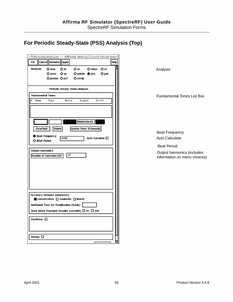
Affirma RF Simulator (SpectreRF) User GuideSpectreRF Simulation Forms
For Periodic Steady-State (PSS) Analysis (Top)
Analysis
Fundamental Tones List Box
Output harmonics (includesinformation on menu choices)
Beat Frequency
Beat Period
Auto Calculate
April 2001 56 Product Version 4.4.6
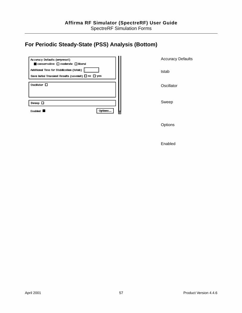
Affirma RF Simulator (SpectreRF) User GuideSpectreRF Simulation Forms
For Periodic Steady-State (PSS) Analysis (Bottom)
Enabled
Options
Accuracy Defaults
tstab
Sweep
Oscillator
April 2001 57 Product Version 4.4.6
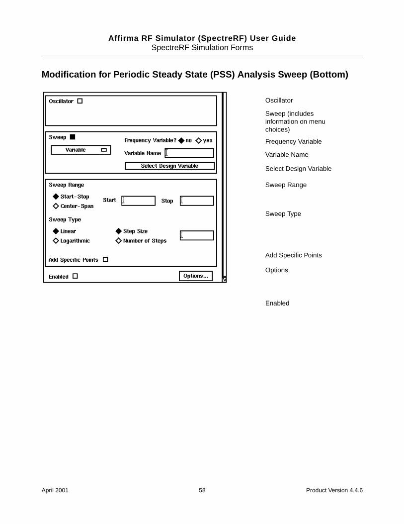
Affirma RF Simulator (SpectreRF) User GuideSpectreRF Simulation Forms
Modification for Periodic Steady State (PSS) Analysis Sweep (Bottom)
Options
Enabled
Add Specific Points
Oscillator
Sweep Type
Sweep Range
Select Design Variable
Variable Name
Sweep (includesinformation on menuchoices)
Frequency Variable
April 2001 58 Product Version 4.4.6
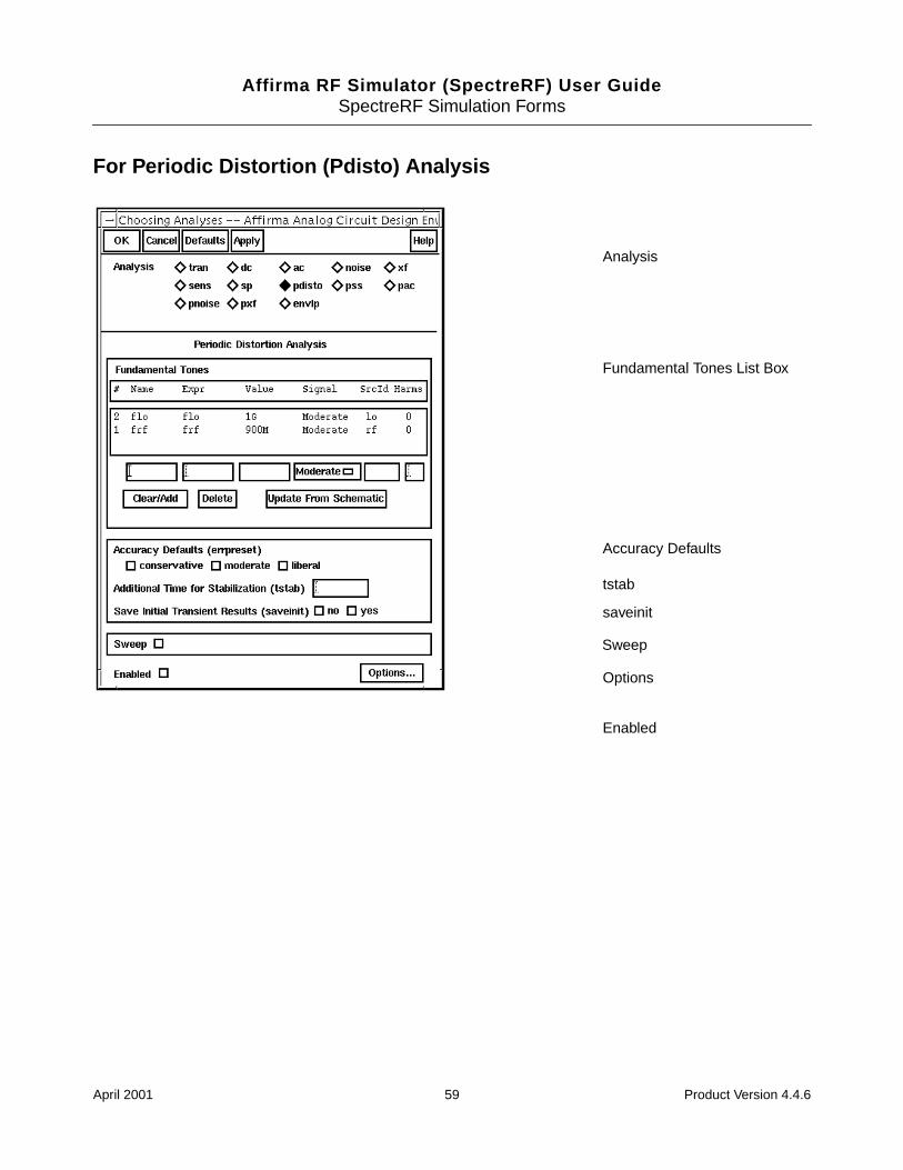
Affirma RF Simulator (SpectreRF) User GuideSpectreRF Simulation Forms
For Periodic Distortion (Pdisto) Analysis
Analysis
Accuracy Defaults
tstab
saveinit
Options
Enabled
Fundamental Tones List Box
Sweep
April 2001 59 Product Version 4.4.6
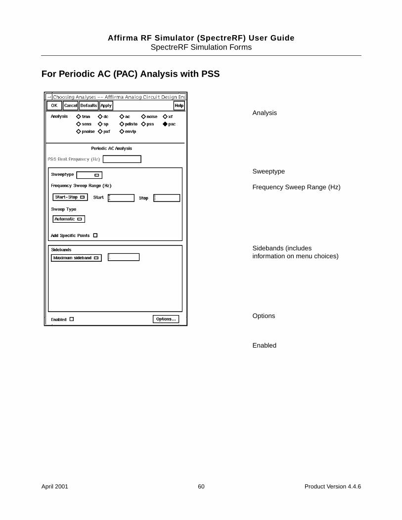
Affirma RF Simulator (SpectreRF) User GuideSpectreRF Simulation Forms
For Periodic AC (PAC) Analysis with PSS
Enabled
Options
Frequency Sweep Range (Hz)
Sweeptype
Sidebands (includesinformation on menu choices)
Analysis
April 2001 60 Product Version 4.4.6
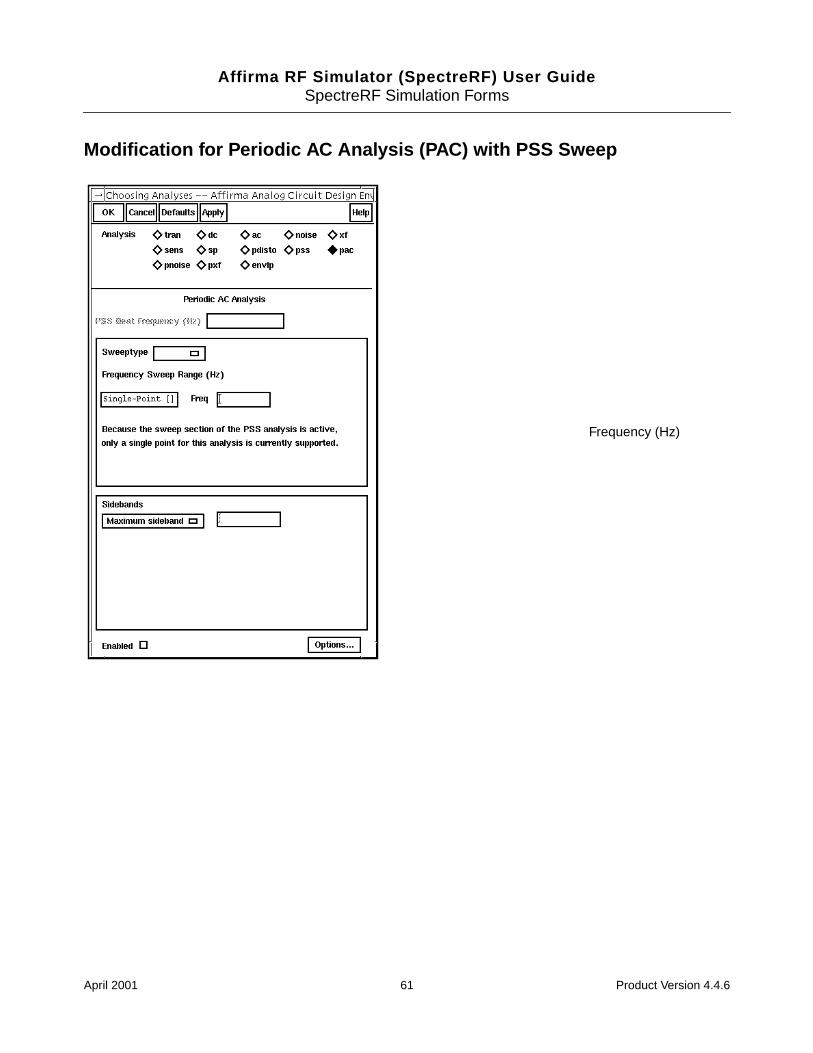
Affirma RF Simulator (SpectreRF) User GuideSpectreRF Simulation Forms
Modification for Periodic AC Analysis (PAC) with PSS Sweep
Frequency (Hz)
April 2001 61 Product Version 4.4.6
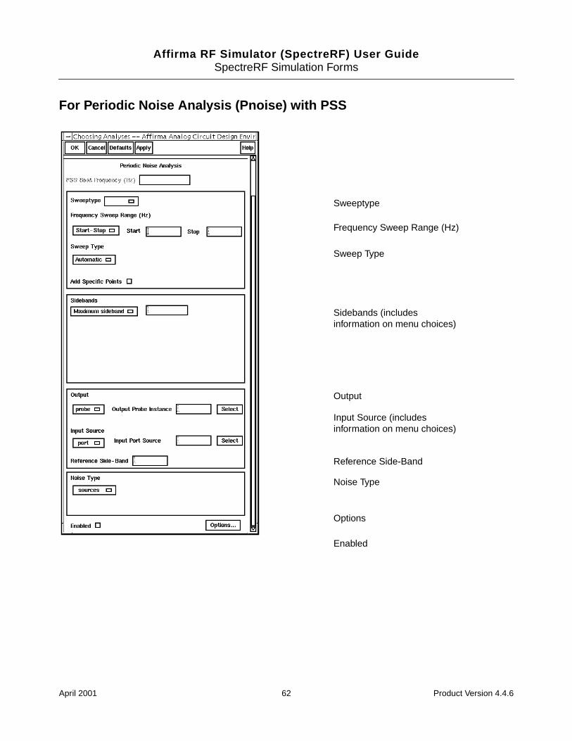
Affirma RF Simulator (SpectreRF) User GuideSpectreRF Simulation Forms
For Periodic Noise Analysis (Pnoise) with PSS
Sweeptype
Sidebands (includesinformation on menu choices)
Output
Input Source (includesinformation on menu choices)
Frequency Sweep Range (Hz)
Enabled
Options
Noise Type
Reference Side-Band
Sweep Type
April 2001 62 Product Version 4.4.6
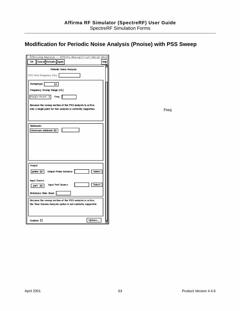
Affirma RF Simulator (SpectreRF) User GuideSpectreRF Simulation Forms
Modification for Periodic Noise Analysis (Pnoise) with PSS Sweep
Freq
April 2001 63 Product Version 4.4.6
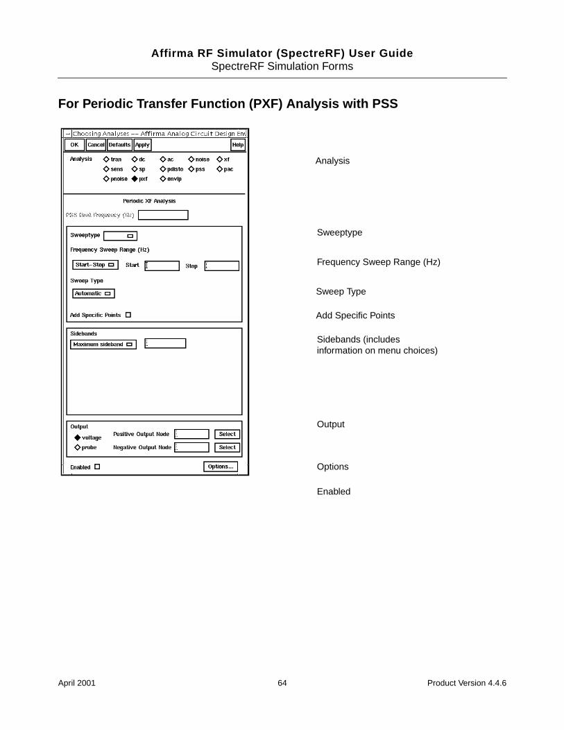
Affirma RF Simulator (SpectreRF) User GuideSpectreRF Simulation Forms
For Periodic Transfer Function (PXF) Analysis with PSS
Frequency Sweep Range (Hz)
Sweeptype
Sidebands (includesinformation on menu choices)
Output
Enabled
Options
Sweep Type
Add Specific Points
Analysis
April 2001 64 Product Version 4.4.6
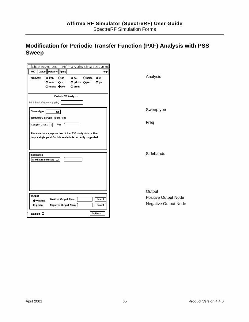
Affirma RF Simulator (SpectreRF) User GuideSpectreRF Simulation Forms
Modification for Periodic Transfer Function (PXF) Analysis with PSSSweep
Freq
Sidebands
Output
Positive Output Node
Negative Output Node
Sweeptype
Analysis
April 2001 65 Product Version 4.4.6
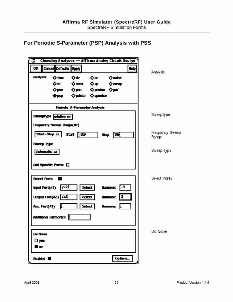
Affirma RF Simulator (SpectreRF) User GuideSpectreRF Simulation Forms
For Periodic S-Parameter (PSP) Analysis with PSS
April 2001 66 Product Version 4.4.6
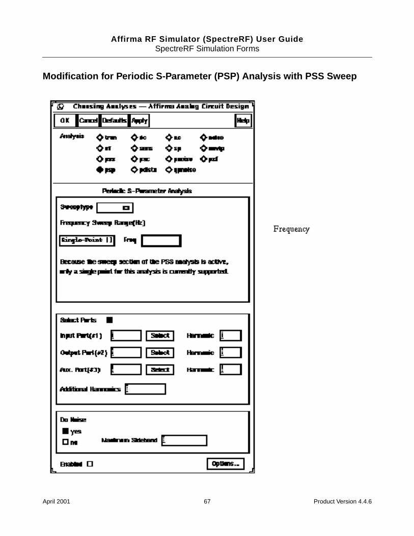
Affirma RF Simulator (SpectreRF) User GuideSpectreRF Simulation Forms
Modification for Periodic S-Parameter (PSP) Analysis with PSS Sweep
April 2001 67 Product Version 4.4.6
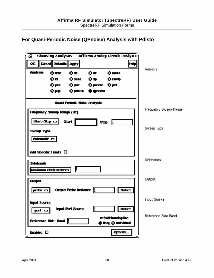
Affirma RF Simulator (SpectreRF) User GuideSpectreRF Simulation Forms
For Quasi-Periodic Noise (QPnoise) Analysis with Pdisto
April 2001 68 Product Version 4.4.6
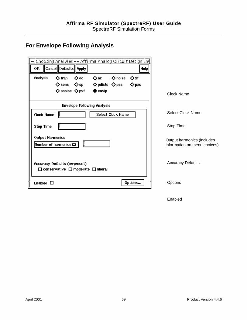
Affirma RF Simulator (SpectreRF) User GuideSpectreRF Simulation Forms
For Envelope Following Analysis
Output harmonics (includesinformation on menu choices)
Clock Name
Select Clock Name
Accuracy Defaults
Options
Enabled
Stop Time
April 2001 69 Product Version 4.4.6
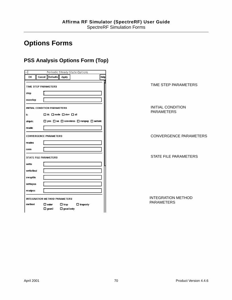
Affirma RF Simulator (SpectreRF) User GuideSpectreRF Simulation Forms
Options Forms
PSS Analysis Options Form (Top)
TIME STEP PARAMETERS
INITIAL CONDITIONPARAMETERS
CONVERGENCE PARAMETERS
STATE FILE PARAMETERS
INTEGRATION METHODPARAMETERS
April 2001 70 Product Version 4.4.6
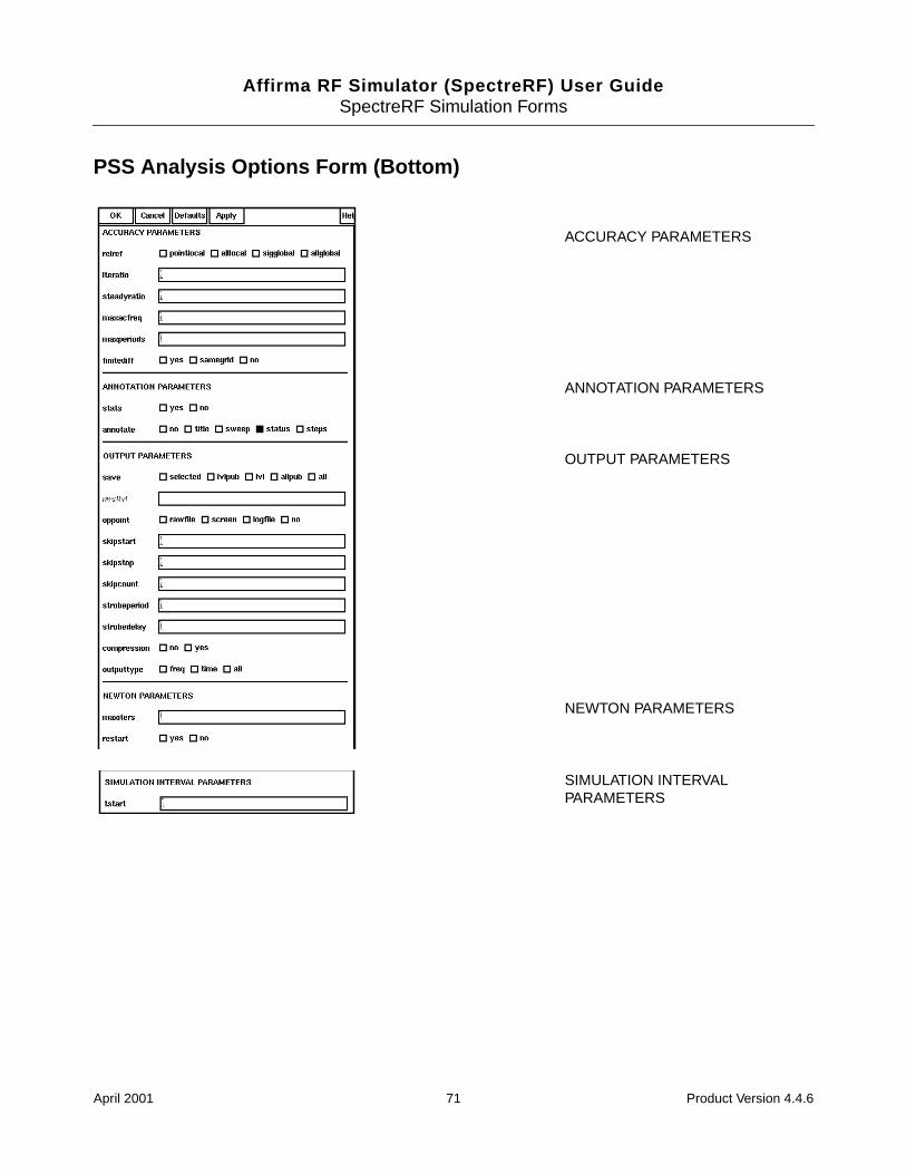
Affirma RF Simulator (SpectreRF) User GuideSpectreRF Simulation Forms
PSS Analysis Options Form (Bottom)
ACCURACY PARAMETERS
ANNOTATION PARAMETERS
OUTPUT PARAMETERS
NEWTON PARAMETERS
SIMULATION INTERVALPARAMETERS
April 2001 71 Product Version 4.4.6
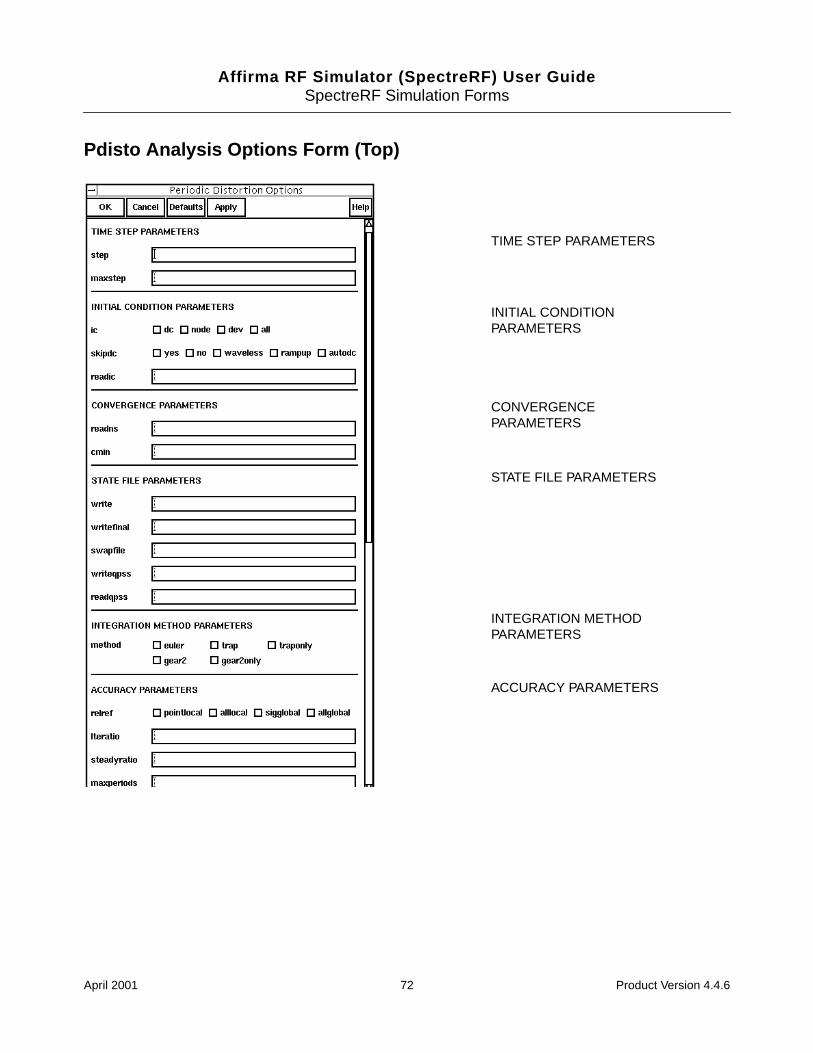
Affirma RF Simulator (SpectreRF) User GuideSpectreRF Simulation Forms
Pdisto Analysis Options Form (Top)
ACCURACY PARAMETERS
INTEGRATION METHODPARAMETERS
STATE FILE PARAMETERS
CONVERGENCEPARAMETERS
INITIAL CONDITIONPARAMETERS
TIME STEP PARAMETERS
April 2001 72 Product Version 4.4.6
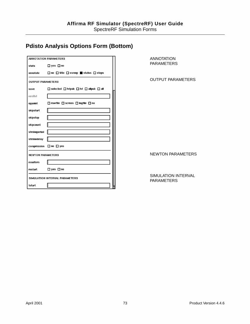
Affirma RF Simulator (SpectreRF) User GuideSpectreRF Simulation Forms
Pdisto Analysis Options Form (Bottom)
SIMULATION INTERVALPARAMETERS
NEWTON PARAMETERS
OUTPUT PARAMETERS
ANNOTATIONPARAMETERS
April 2001 73 Product Version 4.4.6
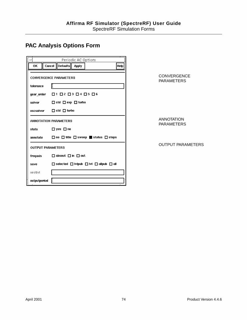
Affirma RF Simulator (SpectreRF) User GuideSpectreRF Simulation Forms
PAC Analysis Options Form
OUTPUT PARAMETERS
ANNOTATIONPARAMETERS
CONVERGENCEPARAMETERS
April 2001 74 Product Version 4.4.6
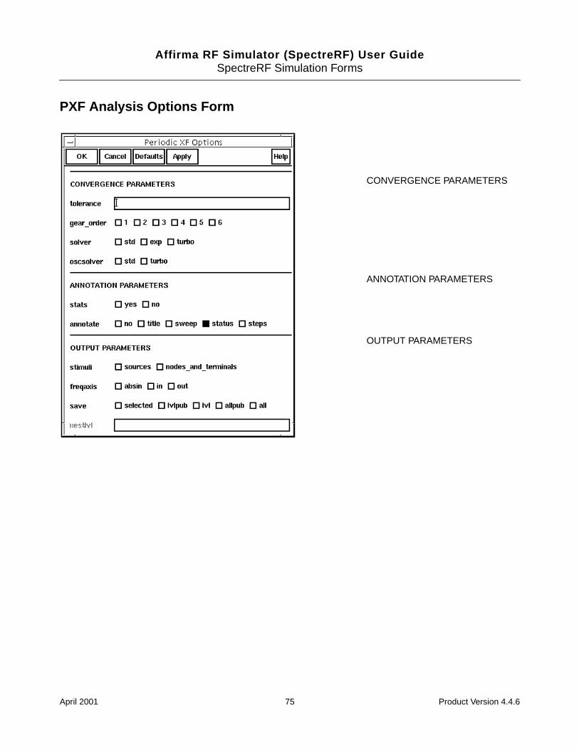
Affirma RF Simulator (SpectreRF) User GuideSpectreRF Simulation Forms
PXF Analysis Options Form
CONVERGENCE PARAMETERS
ANNOTATION PARAMETERS
OUTPUT PARAMETERS
April 2001 75 Product Version 4.4.6
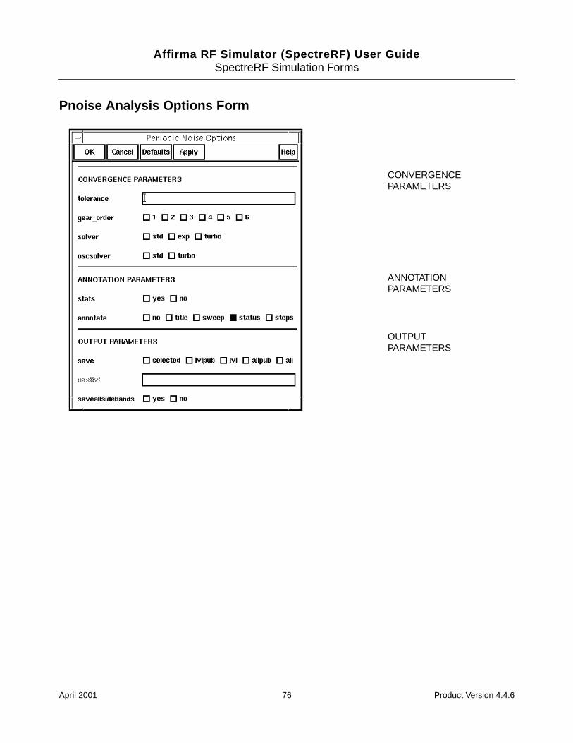
Affirma RF Simulator (SpectreRF) User GuideSpectreRF Simulation Forms
Pnoise Analysis Options Form
OUTPUTPARAMETERS
ANNOTATIONPARAMETERS
CONVERGENCEPARAMETERS
April 2001 76 Product Version 4.4.6
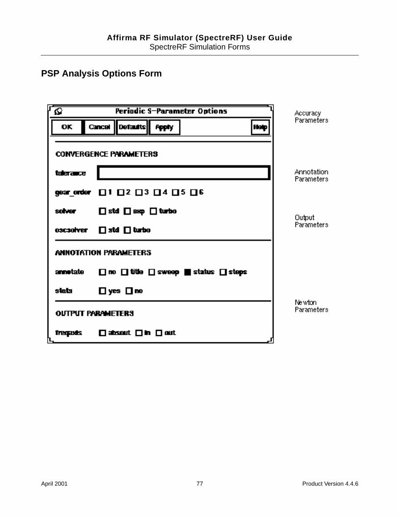
Affirma RF Simulator (SpectreRF) User GuideSpectreRF Simulation Forms
PSP Analysis Options Form
April 2001 77 Product Version 4.4.6
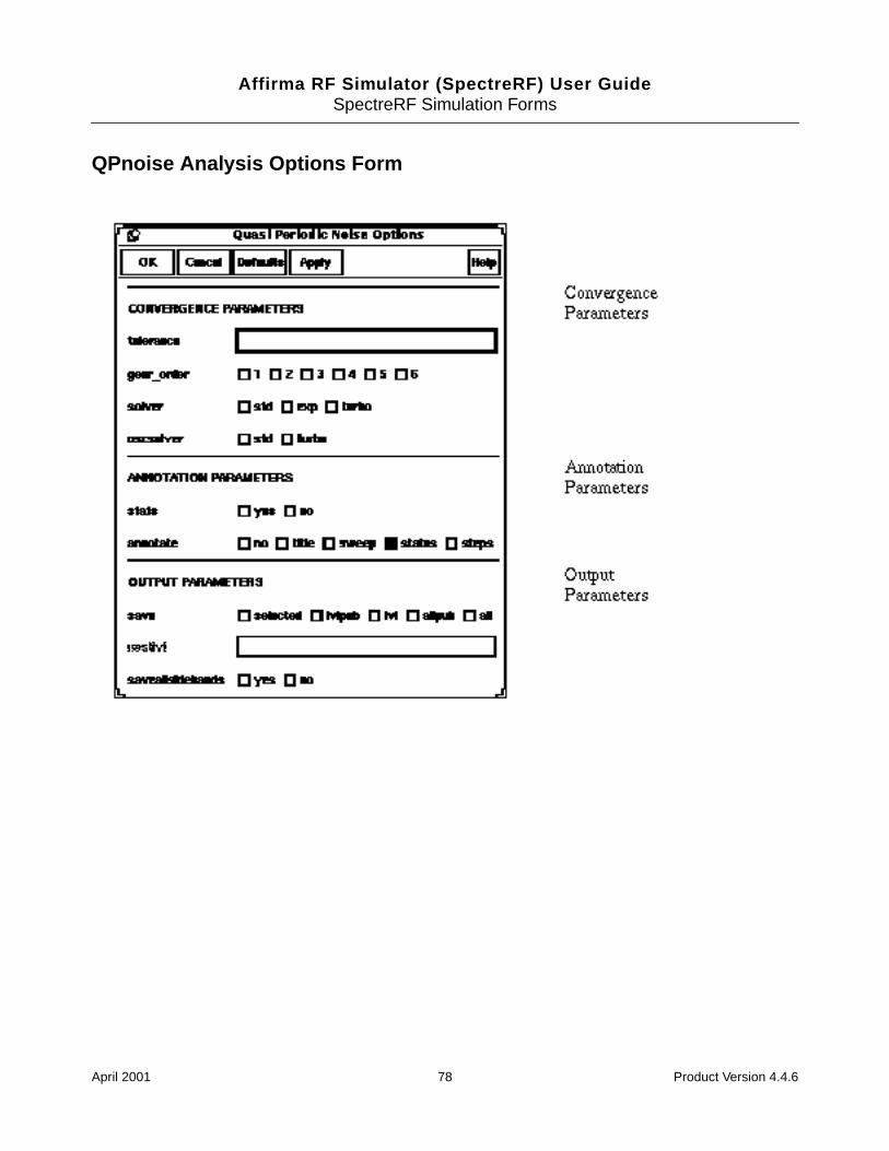
Affirma RF Simulator (SpectreRF) User GuideSpectreRF Simulation Forms
QPnoise Analysis Options Form
April 2001 78 Product Version 4.4.6
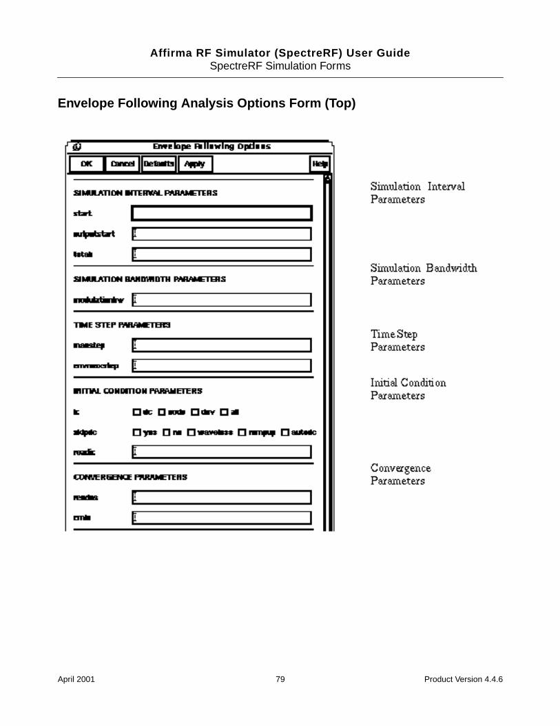
Affirma RF Simulator (SpectreRF) User GuideSpectreRF Simulation Forms
Envelope Following Analysis Options Form (Top)
April 2001 79 Product Version 4.4.6
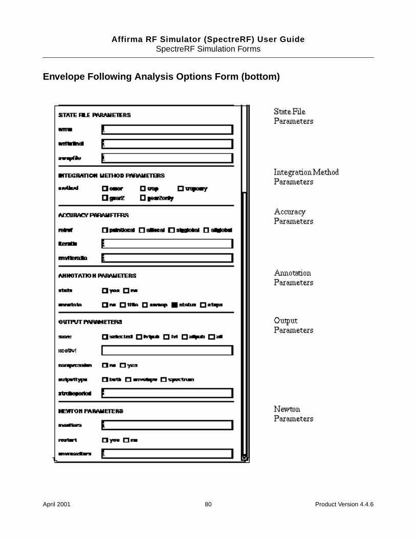
Affirma RF Simulator (SpectreRF) User GuideSpectreRF Simulation Forms
Envelope Following Analysis Options Form (bottom)
April 2001 80 Product Version 4.4.6
Affirma RF Simulator (SpectreRF) User GuideSpectreRF Simulation Forms
Results Forms
You can use Affirma analog circuit design environment direct plot commands to plot mostRF simulation results. There are two Simulation window commands specifically designedfor plotting periodic steady state simulation results:
Results – Direct Plot – PSS
Results – Direct Plot – Pdisto.
Each command opens up a Results form. You define the plots by filling out the PSS orPdisto Results forms and selecting nets or terminals on the schematic.
The plots appear, by default, in the current Affirma analog circuit design environmentWaveform window. If no Waveform window or Schematic window is open, selecting a directplot function automatically opens them both.
For sweeps only, the last section in the form includes a scrolling window that lists differentvalues of the design variable you selected when setting up the analysis. Click on the designvariable values that you want to plot. The name and type of the variable is displayed at thetop of the window. For second and third order intercept functions, the Results form displaysa second list of variable values for the reference variable.
You click on sidebands in a list box to select them. You can select adjacent sidebands byclicking and dragging with the mouse over the sidebands you want to select. To selectsidebands that are not adjacent, hold the Control key down while you click on the individualsidebands. Clicking on a selected sideband while you hold the Control key down deselectsthe sideband.
Spectral Plots and Time Waveforms
Spectral plots show the function level at each frequency component of a single analysis point(one step in a sweep of frequency, input power, or design variable).
To perform a spectral plot:
1. Open the Waveform window, the design schematic, and the PSS Results form bychoosing Results – Direct Plot – PSS.
2. Click on a Plot Mode button to specify if the curves you plot are appended to or replaceexisting curves in the Waveform window.
3. Click on a Function button to select the function you want to plot.
April 2001 81 Product Version 4.4.6
Affirma RF Simulator (SpectreRF) User GuideSpectreRF Simulation Forms
If you need a function that is not included on the PSS Results form, use the RF versionof the Affirma analog circuit design environment calculator.
4. For PSS sweeps, set Sweep to spectrum.
5. Select a plot modifier.
6. To plot a curve in the Waveform window, follow the instructions at the bottom of theResults form.
7. To add the last plot to the Outputs list in the Simulation window, click on the Add toOutputs button and then click on Replot.
When you select a curve to plot from the Outputs list, the expression plotted is alwaysthe magnitude of the signal, not the original modifier. If you want a scale like dB20, youmust modify the expression using Curve – Edit – Scale in the Waveform window orpaste the expression from the Outputs Setup form into the calculator buffer and edit it.
8. To change the noise floor of a spectral plot, use the Axes – Y axis command in theWaveform window, set Range to Min-Max, and specify a Min value.
To use the PSS Results form to plot voltage and current time waveforms, repeat the processfor spectral plots. Set Sweep to time.
April 2001 82 Product Version 4.4.6
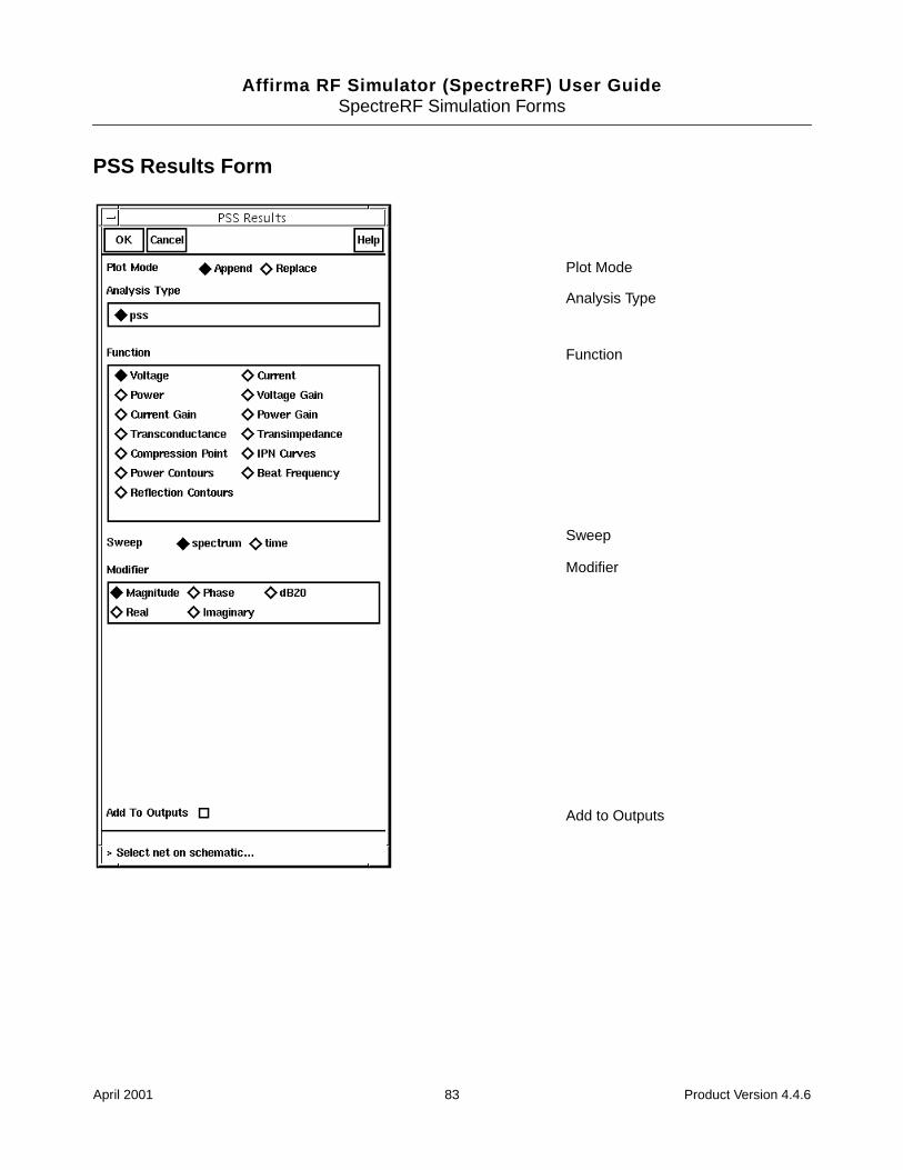
Affirma RF Simulator (SpectreRF) User GuideSpectreRF Simulation Forms
PSS Results Form
Plot Mode
Function
Modifier
Add to Outputs
Analysis Type
Sweep
April 2001 83 Product Version 4.4.6
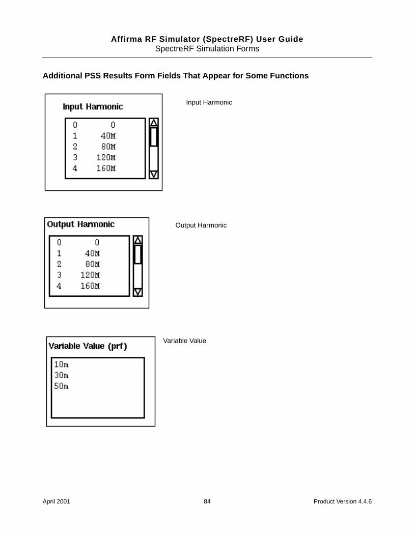
Affirma RF Simulator (SpectreRF) User GuideSpectreRF Simulation Forms
Additional PSS Results Form Fields That Appear for Some Functions
Input Harmonic
Output Harmonic
Variable Value
April 2001 84 Product Version 4.4.6
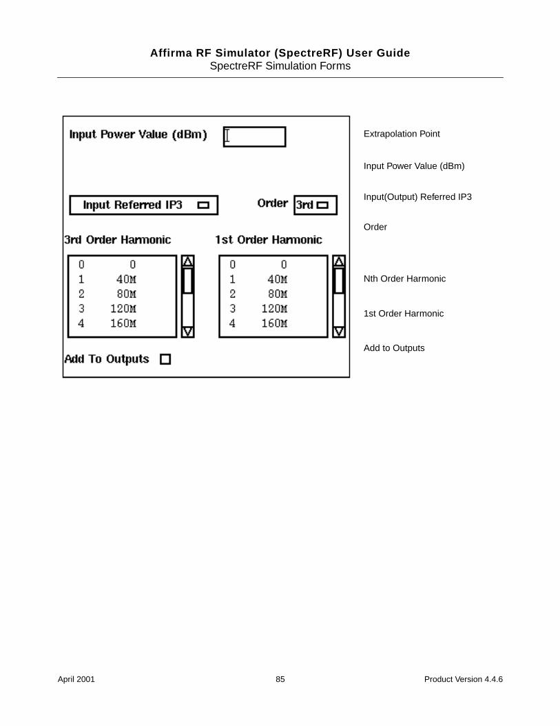
Affirma RF Simulator (SpectreRF) User GuideSpectreRF Simulation Forms
Extrapolation Point
Nth Order Harmonic
1st Order Harmonic
Input Power Value (dBm)
Input(Output) Referred IP3
Order
Add to Outputs
April 2001 85 Product Version 4.4.6
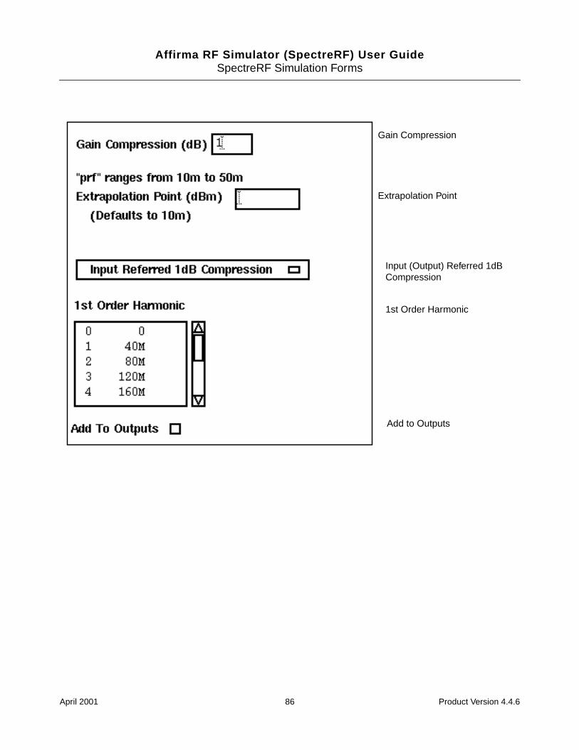
Affirma RF Simulator (SpectreRF) User GuideSpectreRF Simulation Forms
Extrapolation Point
Gain Compression
Input (Output) Referred 1dBCompression
1st Order Harmonic
Add to Outputs
April 2001 86 Product Version 4.4.6
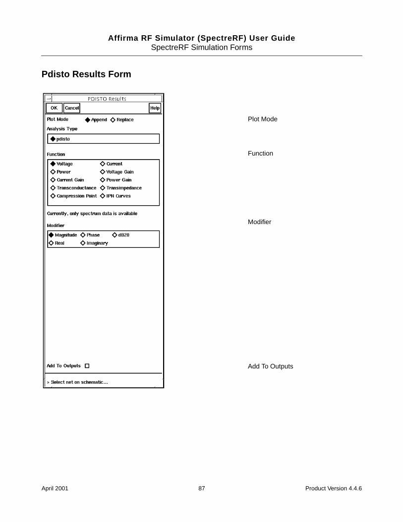
Affirma RF Simulator (SpectreRF) User GuideSpectreRF Simulation Forms
Pdisto Results Form
Plot Mode
Function
Modifier
Add To Outputs
April 2001 87 Product Version 4.4.6
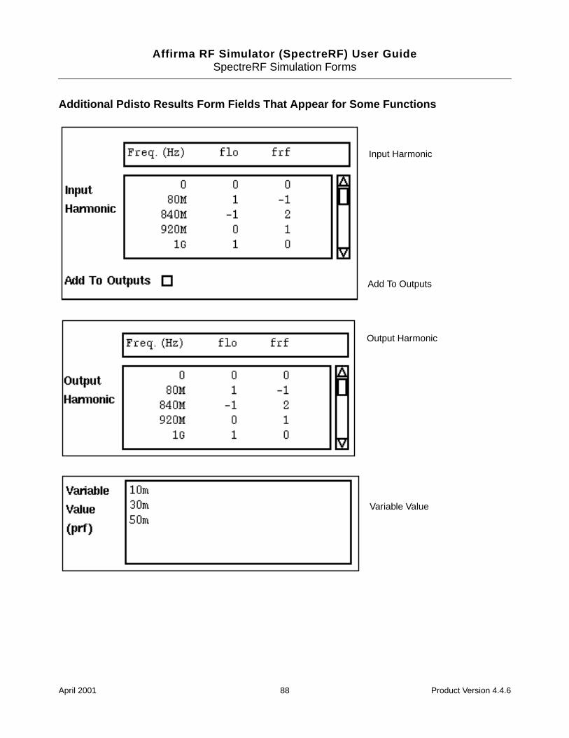
Affirma RF Simulator (SpectreRF) User GuideSpectreRF Simulation Forms
Additional Pdisto Results Form Fields That Appear for Some Functions
Add To Outputs
Input Harmonic
Output Harmonic
Variable Value
April 2001 88 Product Version 4.4.6
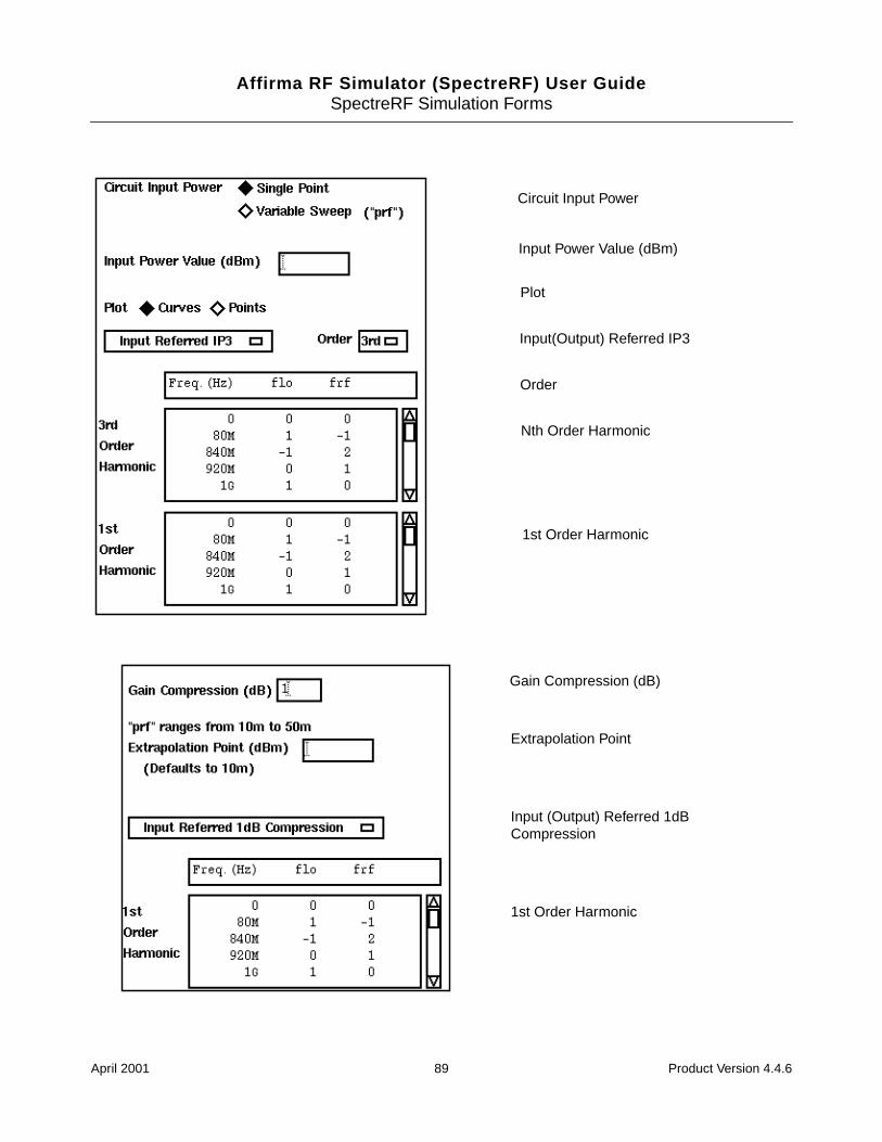
Affirma RF Simulator (SpectreRF) User GuideSpectreRF Simulation Forms
1st Order Harmonic
Nth Order Harmonic
Circuit Input Power
Order
Input(Output) Referred IP3
Plot
Input Power Value (dBm)
Extrapolation Point
Input (Output) Referred 1dBCompression
1st Order Harmonic
Gain Compression (dB)
April 2001 89 Product Version 4.4.6
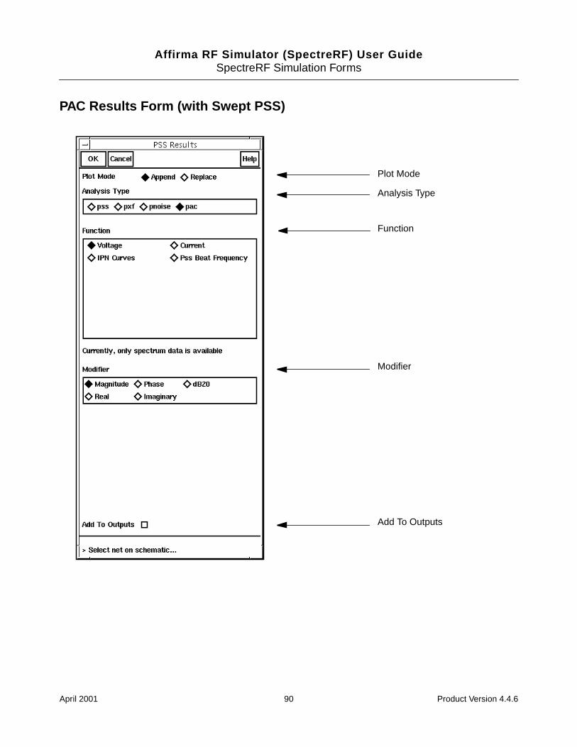
Affirma RF Simulator (SpectreRF) User GuideSpectreRF Simulation Forms
PAC Results Form (with Swept PSS)
Plot Mode
Modifier
Analysis Type
Function
Add To Outputs
April 2001 90 Product Version 4.4.6
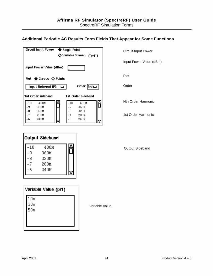
Affirma RF Simulator (SpectreRF) User GuideSpectreRF Simulation Forms
Additional Periodic AC Results Form Fields That Appear for Some Functions
Nth Order Harmonic
Order
1st Order Harmonic
Plot
Input Power Value (dBm)
Circuit Input Power
Output Sideband
Variable Value
April 2001 91 Product Version 4.4.6
Affirma RF Simulator (SpectreRF) User GuideSpectreRF Simulation Forms
Pnoise Results Form (with PSS)
Plot Mode
Modifier
Analysis Type
Function
Plot
Add To Outputs
April 2001 92 Product Version 4.4.6
Affirma RF Simulator (SpectreRF) User GuideSpectreRF Simulation Forms
PXF Results Form (with PSS)
Plot Mode
Analysis Type
Function
Modifier
Add to Outputs
April 2001 93 Product Version 4.4.6
Affirma RF Simulator (SpectreRF) User GuideSpectreRF Simulation Forms
Additional PXF Results Form Fields That Appear for Some Functions
Output Sideband
April 2001 94 Product Version 4.4.6
Affirma RF Simulator (SpectreRF) User GuideSpectreRF Simulation Forms
PSP Results Form (with PSS)
April 2001 95 Product Version 4.4.6
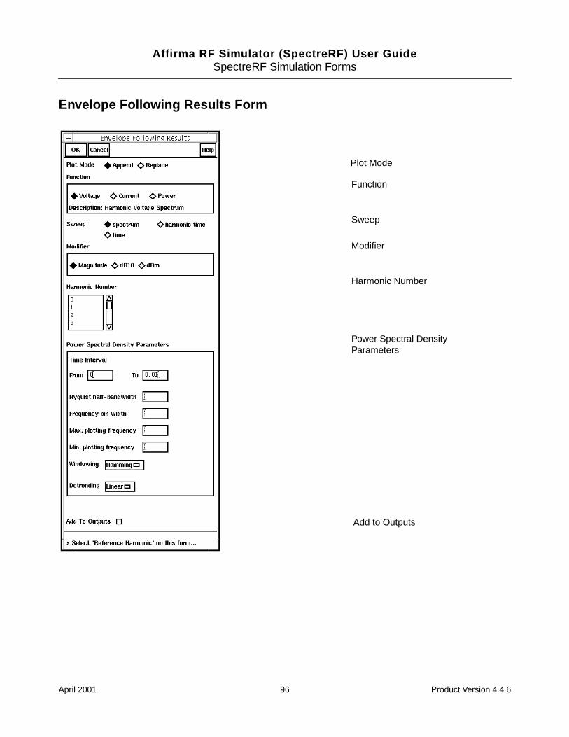
Affirma RF Simulator (SpectreRF) User GuideSpectreRF Simulation Forms
Envelope Following Results Form
Plot Mode
Function
Sweep
Modifier
Harmonic Number
Power Spectral DensityParameters
Add to Outputs
April 2001 96 Product Version 4.4.6
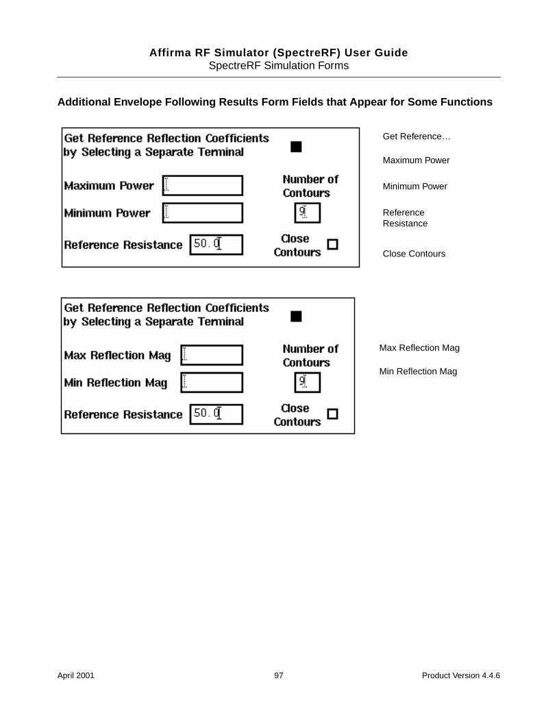
Affirma RF Simulator (SpectreRF) User GuideSpectreRF Simulation Forms
Additional Envelope Following Results Form Fields that Appear for Some Functions
Get Reference…
Maximum Power
Minimum Power
ReferenceResistance
Close Contours
Min Reflection Mag
Max Reflection Mag
April 2001 97 Product Version 4.4.6
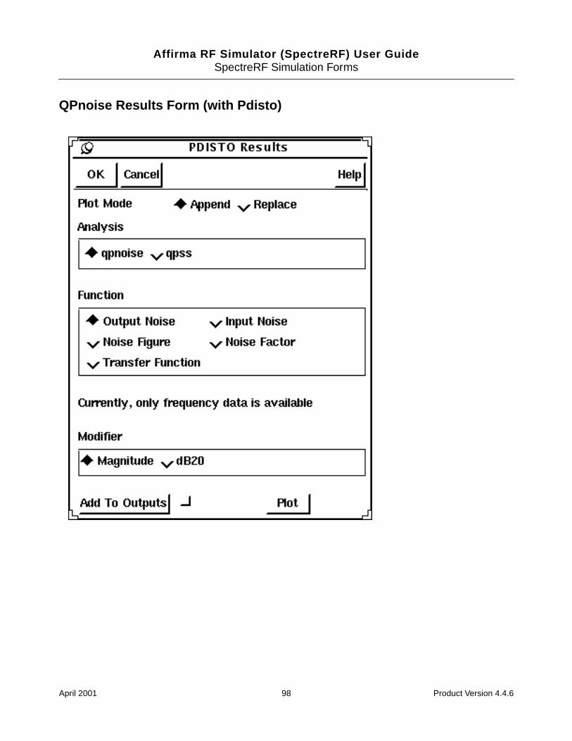
Affirma RF Simulator (SpectreRF) User GuideSpectreRF Simulation Forms
QPnoise Results Form (with Pdisto)
April 2001 98 Product Version 4.4.6
Affirma RF Simulator (SpectreRF) User GuideSpectreRF Simulation Forms
Form Field Descriptions
The remaining sections of this chapter presents text descriptions for the SpectreRF forms.
Choosing Analysis Form
The Options Forms for each analysis
The Results Forms for each analysis
The text description topics are presented alphabetically, according to the top-level headingson the forms. The top-level headings are usually found at the leftmost margin of the form.
Choosing Analysis Form
Accuracy Defaults (errpreset)
Lets you adjust the simulator parameters to fit your needs quickly. You can set errpreset toconservative if the circuit is very sensitive, or you can set it to liberal for a fast. butpossibly inaccurate, simulation. The setting errpreset=moderate suits most needs.
The effect of errpreset on other parameters is shown in the following table. In this table, T=stop - start.
The value of reltol is increased or decreased from its value in the options statement, but itis not allowed to be larger than 0.01. Spectre simulation sets the value of maxstep so thatit is no larger than the value given in the table. Except for reltol and maxstep, errpresetdoes not change the value of any parameters you have explicitly set. The actual values usedfor the transient analysis are given in the log file.
errpreset reltol relref method maxstep lteratio
liberal ×10.0 allglobal gear2 <=T/10 3.5
moderate ×1.0 sigglobal traponly <=T/50 3.5
conservative ×0.1 alllocal gear2only <=T/100 10.0
April 2001 99 Product Version 4.4.6
Affirma RF Simulator (SpectreRF) User GuideSpectreRF Simulation Forms
Additional Time for Stabilization (tstab)
The amount of additional time that you specify to allow the circuit to settle. Use tstab if thecircuit exhibits more than one periodic solution and you want only one. A long tstab can alsoimprove convergence.
Add Specific Points
See Sweep Type.
Analysis
Selects the SpectreRF analysis type.
The RF analyses are
The periodic large-signal pss analysis
The periodic medium-signal pdisto (qpss) analysis
The periodic small-signal analyses: pac, psp, pnoise, and pxf
The quasi-periodic small-signal qpnoise analysis
You can run the small-signal analyses after a large-signal analysis.
Auto Calculate Button
When selected, the Choosing Analysis form will automatically calculate the Beat Frequencyand Beat Period field value based on the tones present in the Fundamental Tones list box.The value of the frequency will be the greatest common multiple of all the tone frequenciesthat are not small signal. The period will be set to the inverse of the frequency.
Beat Frequency
When you open the Choosing Analysis form, this type-in field is empty. Entering a value intothis field can be accomplished in two ways. You can type in a value in which all the tonefrequencies must be an integer multiple of the value, or you can click the Auto Calculatebutton so the Choosing Analysis form automatically calculates and enters a value intothe field.
April 2001 100 Product Version 4.4.6
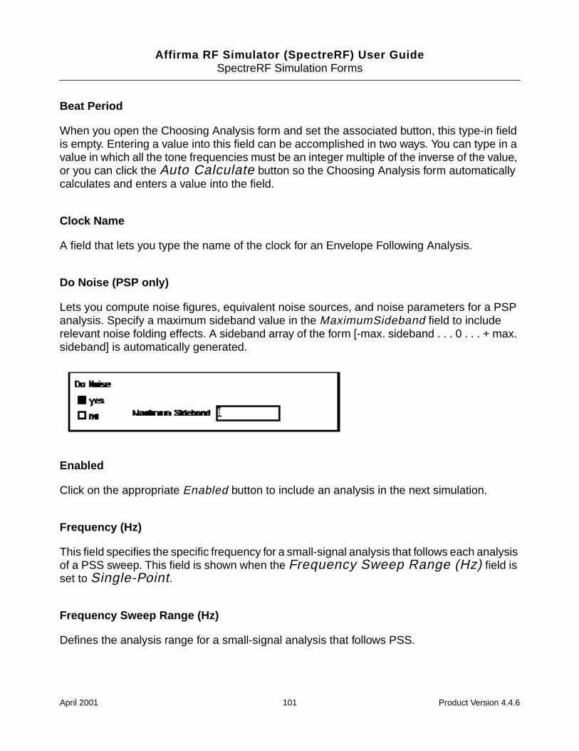
Affirma RF Simulator (SpectreRF) User GuideSpectreRF Simulation Forms
Beat Period
When you open the Choosing Analysis form and set the associated button, this type-in fieldis empty. Entering a value into this field can be accomplished in two ways. You can type in avalue in which all the tone frequencies must be an integer multiple of the inverse of the value,or you can click the Auto Calculate button so the Choosing Analysis form automaticallycalculates and enters a value into the field.
Clock Name
A field that lets you type the name of the clock for an Envelope Following Analysis.
Do Noise (PSP only)
Lets you compute noise figures, equivalent noise sources, and noise parameters for a PSPanalysis. Specify a maximum sideband value in the MaximumSideband field to includerelevant noise folding effects. A sideband array of the form [-max. sideband . . . 0 . . . + max.sideband] is automatically generated.
Enabled
Click on the appropriate Enabled button to include an analysis in the next simulation.
Frequency (Hz)
This field specifies the specific frequency for a small-signal analysis that follows each analysisof a PSS sweep. This field is shown when the Frequency Sweep Range (Hz) field isset to Single-Point.
Frequency Sweep Range (Hz)
Defines the analysis range for a small-signal analysis that follows PSS.
April 2001 101 Product Version 4.4.6
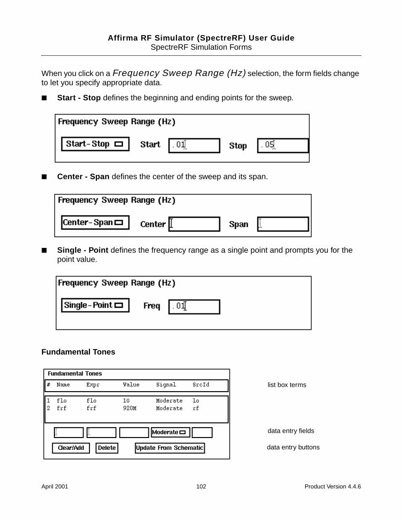
Affirma RF Simulator (SpectreRF) User GuideSpectreRF Simulation Forms
When you click on a Frequency Sweep Range (Hz) selection, the form fields changeto let you specify appropriate data.
Start - Stop defines the beginning and ending points for the sweep.
Center - Span defines the center of the sweep and its span.
Single - Point defines the frequency range as a single point and prompts you for thepoint value.
Fundamental Tones
data entry fields
data entry buttons
list box terms
April 2001 102 Product Version 4.4.6
Affirma RF Simulator (SpectreRF) User GuideSpectreRF Simulation Forms
Fundamental Tones list box – This section appears in the Choosing Analysis form for thePSS and Pdisto analyses. The Fundamental Tones list box displays information aboutevery top-level tone in the circuit that has both a non-zero frequency or period value, and anon-zero amplitude value (absolute). For each tone entry, you can edit either the Signallevel designation or the Harms value (Pdisto only). Edits are performed by selecting a tonerow and then editing the data entry fields.
For tones that are not at the top level of the schematic, you must manually insert a tone entryinto the list box by entering the pertinent information into the data entry fields.
All tones in the list box are arranged alphabetically by name.
Each name and correlated frequency value of non-small-signal tones are used in the Selectfrom range and Array of coefficients fields in the harmonics and sidebands sectionsof the PSS, PAC, PNOISE and PXF analysis forms.
List Box Terms and Corresponding Data Entry Fields
Name – Displays the name assigned to each tone. This name must be entered intothe pertinent Component Description Format (CDF) fields of each source in theschematic with a tone. The current CDF name field prompts are “First frequencyname”, “Second frequency name”, “Frequency name”, and “Frequency name for 1/period”.
Expr – Displays the value or expression representing the frequency of a particulartone. The expression can also be a user variable or contain user variables. If thefrequency for the tone is specified in a variable, this field displays the name of thevariable. Otherwise, the field displays the numerical value of the frequency.
Value – Displays the evaluated value of the Expr field using the current values ofthe user variables.
Signal – This field displays one of three values: Large, Moderate, or Small.You must select a single Large tone for Pdisto, and this is the only time you usethe Large specification. Specify all other tones for Pdisto simulation asModerate. For PSS, specify Moderate for all tones you want to include in thesimulation. Tones that you specify as Small are ignored by PSS and Pdisto.
SrcId – Displays the instance name of the source in the schematic where the toneis declared.
To specify a new tone, make sure there are no selected tones in the list box. If athere is a selected tone, click the Clear/Add button. Next, enter a value into anyof the data entry fields (typically starting with the name field). As you advance to asecond data entry field, a new tone line will automatically be added to the list boxand become selected. Continue editing all the data entry fields until all the pertinent
April 2001 103 Product Version 4.4.6
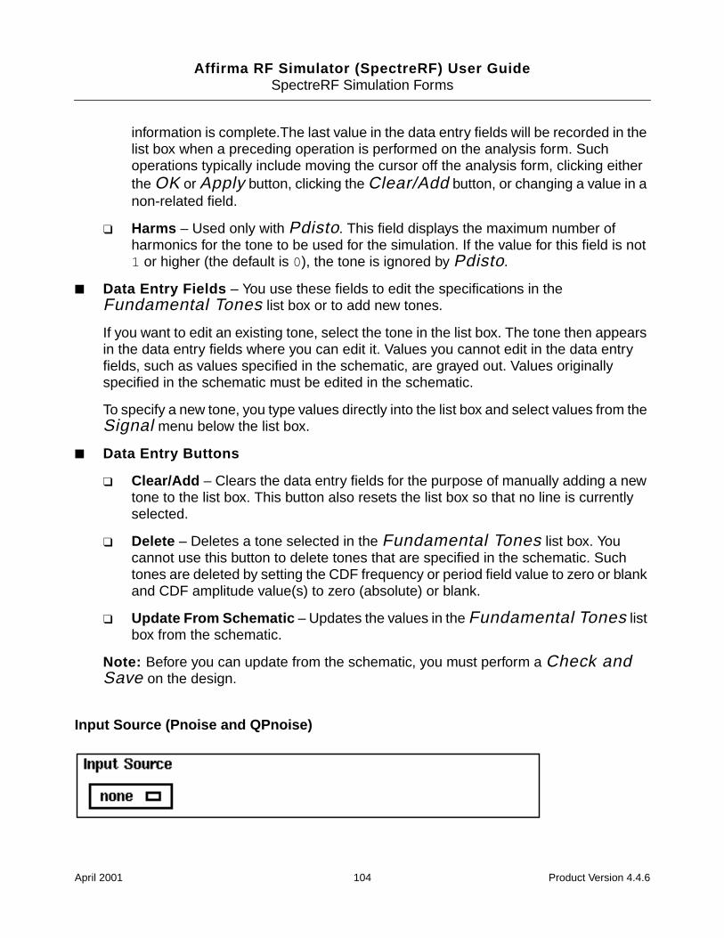
Affirma RF Simulator (SpectreRF) User GuideSpectreRF Simulation Forms
information is complete.The last value in the data entry fields will be recorded in thelist box when a preceding operation is performed on the analysis form. Suchoperations typically include moving the cursor off the analysis form, clicking eitherthe OK or Apply button, clicking the Clear/Add button, or changing a value in anon-related field.
Harms – Used only with Pdisto. This field displays the maximum number ofharmonics for the tone to be used for the simulation. If the value for this field is not1 or higher (the default is 0), the tone is ignored by Pdisto.
Data Entry Fields – You use these fields to edit the specifications in theFundamental Tones list box or to add new tones.
If you want to edit an existing tone, select the tone in the list box. The tone then appearsin the data entry fields where you can edit it. Values you cannot edit in the data entryfields, such as values specified in the schematic, are grayed out. Values originallyspecified in the schematic must be edited in the schematic.
To specify a new tone, you type values directly into the list box and select values from theSignal menu below the list box.
Data Entry Buttons
Clear/Add – Clears the data entry fields for the purpose of manually adding a newtone to the list box. This button also resets the list box so that no line is currentlyselected.
Delete – Deletes a tone selected in the Fundamental Tones list box. Youcannot use this button to delete tones that are specified in the schematic. Suchtones are deleted by setting the CDF frequency or period field value to zero or blankand CDF amplitude value(s) to zero (absolute) or blank.
Update From Schematic – Updates the values in the Fundamental Tones listbox from the schematic.
Note: Before you can update from the schematic, you must perform a Check andSave on the design.
Input Source (Pnoise and QPnoise)
April 2001 104 Product Version 4.4.6
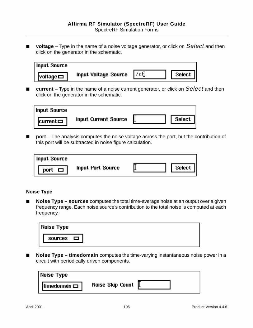
Affirma RF Simulator (SpectreRF) User GuideSpectreRF Simulation Forms
voltage – Type in the name of a noise voltage generator, or click on Select and thenclick on the generator in the schematic.
current – Type in the name of a noise current generator, or click on Select and thenclick on the generator in the schematic.
port – The analysis computes the noise voltage across the port, but the contribution ofthis port will be subtracted in noise figure calculation.
Noise Type
Noise Type – sources computes the total time-average noise at an output over a givenfrequency range. Each noise source’s contribution to the total noise is computed at eachfrequency.
Noise Type – timedomain computes the time-varying instantaneous noise power in acircuit with periodically driven components.
April 2001 105 Product Version 4.4.6
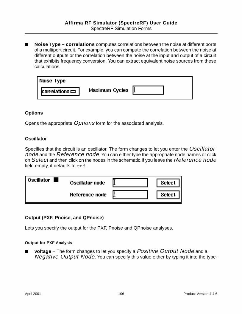
Affirma RF Simulator (SpectreRF) User GuideSpectreRF Simulation Forms
Noise Type – correlations computes correlations between the noise at different portsof a multiport circuit. For example, you can compute the correlation between the noise atdifferent outputs or the correlation between the noise at the input and output of a circuitthat exhibits frequency conversion. You can extract equivalent noise sources from thesecalculations.
Options
Opens the appropriate Options form for the associated analysis.
Oscillator
Specifies that the circuit is an oscillator. The form changes to let you enter the Oscillatornode and the Reference node. You can either type the appropriate node names or clickon Select and then click on the nodes in the schematic.If you leave the Reference nodefield empty, it defaults to gnd .
Output (PXF, Pnoise, and QPnoise)
Lets you specify the output for the PXF, Pnoise and QPnoise analyses.
Output for PXF Analysis
voltage – The form changes to let you specify a Positive Output Node and aNegative Output Node. You can specify this value either by typing it into the type-
April 2001 106 Product Version 4.4.6
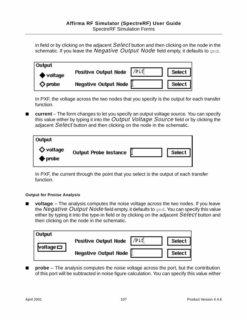
Affirma RF Simulator (SpectreRF) User GuideSpectreRF Simulation Forms
in field or by clicking on the adjacent Select button and then clicking on the node in theschematic. If you leave the Negative Output Node field empty, it defaults to gnd .
In PXF, the voltage across the two nodes that you specify is the output for each transferfunction.
current – The form changes to let you specify an output voltage source. You can specifythis value either by typing it into the Output Voltage Source field or by clicking theadjacent Select button and then clicking on the node in the schematic.
In PXF, the current through the point that you select is the output of each transferfunction.
Output for Pnoise Analysis
voltage – The analysis computes the noise voltage across the two nodes. If you leavethe Negative Output Node field empty, it defaults to gnd . You can specify this valueeither by typing it into the type-in field or by clicking on the adjacent Select button andthen clicking on the node in the schematic.
probe – The analysis computes the noise voltage across the port, but the contributionof this port will be subtracted in noise figure calculation. You can specify this value either
April 2001 107 Product Version 4.4.6
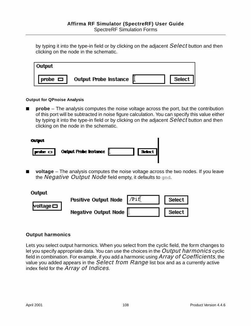
Affirma RF Simulator (SpectreRF) User GuideSpectreRF Simulation Forms
by typing it into the type-in field or by clicking on the adjacent Select button and thenclicking on the node in the schematic.
Output for QPnoise Analysis
probe – The analysis computes the noise voltage across the port, but the contributionof this port will be subtracted in noise figure calculation. You can specify this value eitherby typing it into the type-in field or by clicking on the adjacent Select button and thenclicking on the node in the schematic.
voltage – The analysis computes the noise voltage across the two nodes. If you leavethe Negative Output Node field empty, it defaults to gnd .
Output harmonics
Lets you select output harmonics. When you select from the cyclic field, the form changes tolet you specify appropriate data. You can use the choices in the Output harmonics cyclicfield in combination. For example, if you add a harmonic using Array of Coefficients, thevalue you added appears in the Select from Range list box and as a currently activeindex field for the Array of Indices.
April 2001 108 Product Version 4.4.6
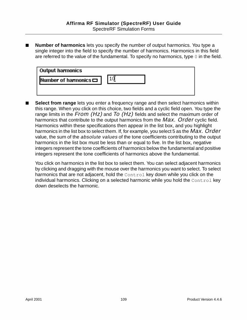
Affirma RF Simulator (SpectreRF) User GuideSpectreRF Simulation Forms
Number of harmonics lets you specify the number of output harmonics. You type asingle integer into the field to specify the number of harmonics. Harmonics in this fieldare referred to the value of the fundamental. To specify no harmonics, type 0 in the field.
Select from range lets you enter a frequency range and then select harmonics withinthis range. When you click on this choice, two fields and a cyclic field open. You type therange limits in the From (Hz) and To (Hz) fields and select the maximum order ofharmonics that contribute to the output harmonics from the Max. Order cyclic field.Harmonics within these specifications then appear in the list box, and you highlightharmonics in the list box to select them. If, for example, you select 5 as the Max. Ordervalue, the sum of the absolute values of the tone coefficients contributing to the outputharmonics in the list box must be less than or equal to five. In the list box, negativeintegers represent the tone coefficients of harmonics below the fundamental and positiveintegers represent the tone coefficients of harmonics above the fundamental.
You click on harmonics in the list box to select them. You can select adjacent harmonicsby clicking and dragging with the mouse over the harmonics you want to select. To selectharmonics that are not adjacent, hold the Control key down while you click on theindividual harmonics. Clicking on a selected harmonic while you hold the Control keydown deselects the harmonic.
April 2001 109 Product Version 4.4.6
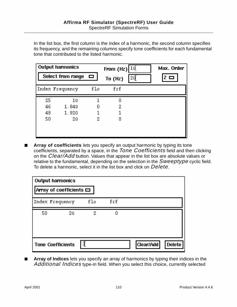
Affirma RF Simulator (SpectreRF) User GuideSpectreRF Simulation Forms
In the list box, the first column is the index of a harmonic, the second column specifiesits frequency, and the remaining columns specify tone coefficients for each fundamentaltone that contributed to the listed harmonic.
Array of coefficients lets you specify an output harmonic by typing its tonecoefficients, separated by a space, in the Tone Coefficients field and then clickingon the Clear/Add button. Values that appear in the list box are absolute values orrelative to the fundamental, depending on the selection in the Sweeptype cyclic field.To delete a harmonic, select it in the list box and click on Delete.
Array of Indices lets you specify an array of harmonics by typing their indices in theAdditional Indices type-in field. When you select this choice, currently selected
April 2001 110 Product Version 4.4.6
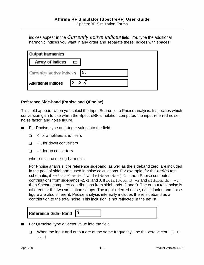
Affirma RF Simulator (SpectreRF) User GuideSpectreRF Simulation Forms
indices appear in the Currently active indices field. You type the additionalharmonic indices you want in any order and separate these indices with spaces.
Reference Side-band (Pnoise and QPnoise)
This field appears when you select the Input Source for a Pnoise analysis. It specifies whichconversion gain to use when the SpectreRF simulation computes the input-referred noise,noise factor, and noise figure.
For Pnoise, type an integer value into the field.
0 for amplifiers and filters
-K for down converters
+K for up converters
where K is the mixing harmonic.
For Pnoise analysis, the reference sideband, as well as the sideband zero, are includedin the pool of sidebands used in noise calculations. For example, for the ne600 testschematic, if refsideband=-1 and sidebands=[-2] , then Pnoise computescontributions from sidebands -2, -1, and 0. If refsideband=-2 and sidebands=[-2] ,then Spectre computes contributions from sidebands -2 and 0. The output total noise isdifferent for the two simulation setups. The input-referred noise, noise factor, and noisefigure are also different. Pnoise analysis internally includes the refsideband as acontribution to the total noise. This inclusion is not reflected in the netlist.
For QPnoise, type a vector value into the field.
When the input and output are at the same frequency, use the zero vector [0 0...]
April 2001 111 Product Version 4.4.6
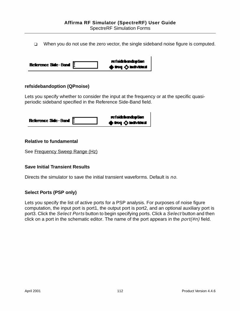
Affirma RF Simulator (SpectreRF) User GuideSpectreRF Simulation Forms
When you do not use the zero vector, the single sideband noise figure is computed.
refsidebandoption (QPnoise)
Lets you specify whether to consider the input at the frequency or at the specific quasi-periodic sideband specified in the Reference Side-Band field.
Relative to fundamental
See Frequency Sweep Range (Hz)
Save Initial Transient Results
Directs the simulator to save the initial transient waveforms. Default is no.
Select Ports (PSP only)
Lets you specify the list of active ports for a PSP analysis. For purposes of noise figurecomputation, the input port is port1, the output port is port2, and an optional auxiliary port isport3. Click the Select Ports button to begin specifying ports. Click a Select button and thenclick on a port in the schematic editor. The name of the port appears in the port(#n) field.
April 2001 112 Product Version 4.4.6
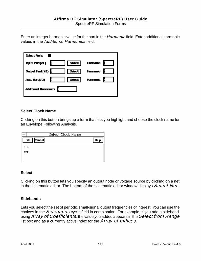
Affirma RF Simulator (SpectreRF) User GuideSpectreRF Simulation Forms
Enter an integer harmonic value for the port in the Harmonic field. Enter additional harmonicvalues in the Additional Harmonics field.
Select Clock Name
Clicking on this button brings up a form that lets you highlight and choose the clock name foran Envelope Following Analysis.
Select
Clicking on this button lets you specify an output node or voltage source by clicking on a netin the schematic editor. The bottom of the schematic editor window displays Select Net.
Sidebands
Lets you select the set of periodic small-signal output frequencies of interest. You can use thechoices in the Sidebands cyclic field in combination. For example, if you add a sidebandusing Array of Coefficients, the value you added appears in the Select from Rangelist box and as a currently active index for the Array of Indices.
April 2001 113 Product Version 4.4.6
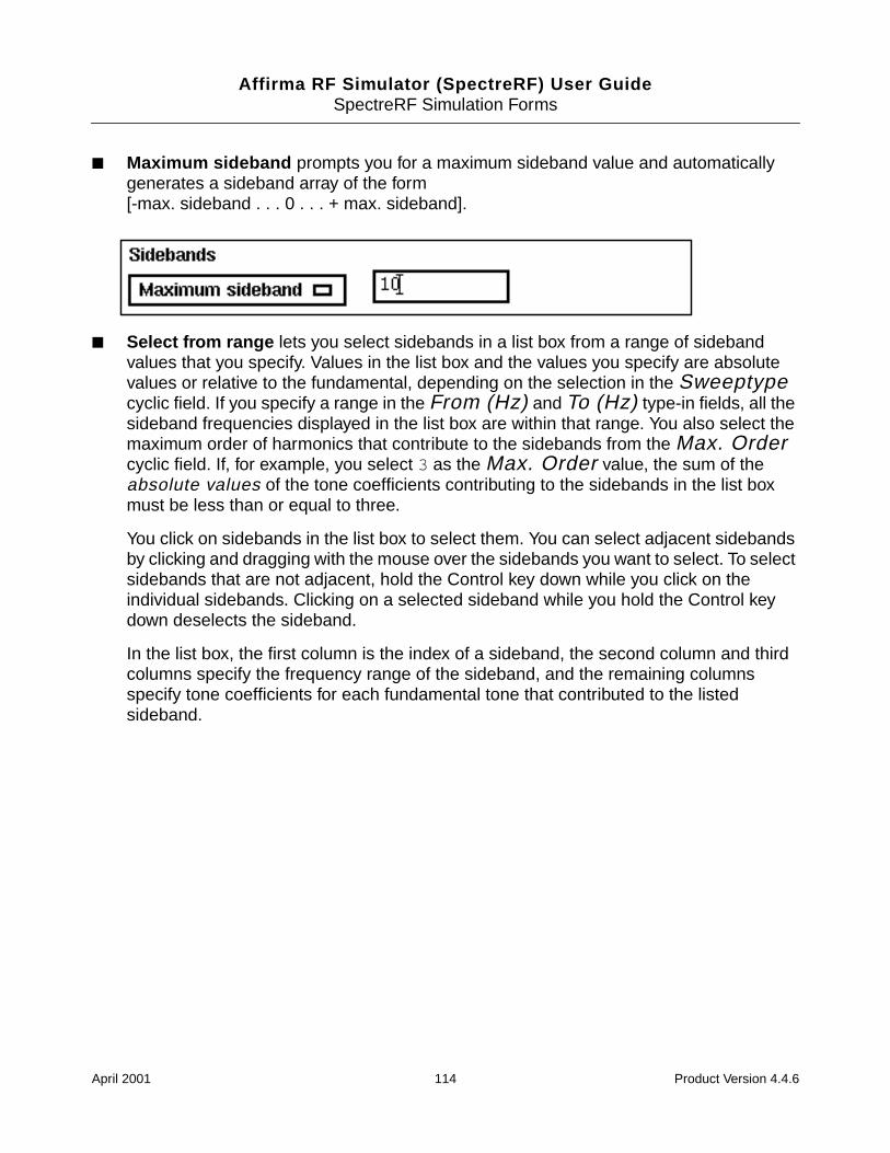
Affirma RF Simulator (SpectreRF) User GuideSpectreRF Simulation Forms
Maximum sideband prompts you for a maximum sideband value and automaticallygenerates a sideband array of the form[-max. sideband . . . 0 . . . + max. sideband].
Select from range lets you select sidebands in a list box from a range of sidebandvalues that you specify. Values in the list box and the values you specify are absolutevalues or relative to the fundamental, depending on the selection in the Sweeptypecyclic field. If you specify a range in the From (Hz) and To (Hz) type-in fields, all thesideband frequencies displayed in the list box are within that range. You also select themaximum order of harmonics that contribute to the sidebands from the Max. Ordercyclic field. If, for example, you select 3 as the Max. Order value, the sum of theabsolute values of the tone coefficients contributing to the sidebands in the list boxmust be less than or equal to three.
You click on sidebands in the list box to select them. You can select adjacent sidebandsby clicking and dragging with the mouse over the sidebands you want to select. To selectsidebands that are not adjacent, hold the Control key down while you click on theindividual sidebands. Clicking on a selected sideband while you hold the Control keydown deselects the sideband.
In the list box, the first column is the index of a sideband, the second column and thirdcolumns specify the frequency range of the sideband, and the remaining columnsspecify tone coefficients for each fundamental tone that contributed to the listedsideband.
April 2001 114 Product Version 4.4.6
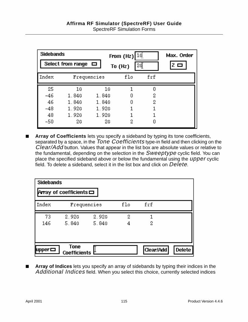
Affirma RF Simulator (SpectreRF) User GuideSpectreRF Simulation Forms
Array of Coefficients lets you specify a sideband by typing its tone coefficients,separated by a space, in the Tone Coefficients type-in field and then clicking on theClear/Add button. Values that appear in the list box are absolute values or relative tothe fundamental, depending on the selection in the Sweeptype cyclic field. You canplace the specified sideband above or below the fundamental using the upper cyclicfield. To delete a sideband, select it in the list box and click on Delete.
Array of Indices lets you specify an array of sidebands by typing their indices in theAdditional Indices field. When you select this choice, currently selected indices
April 2001 115 Product Version 4.4.6
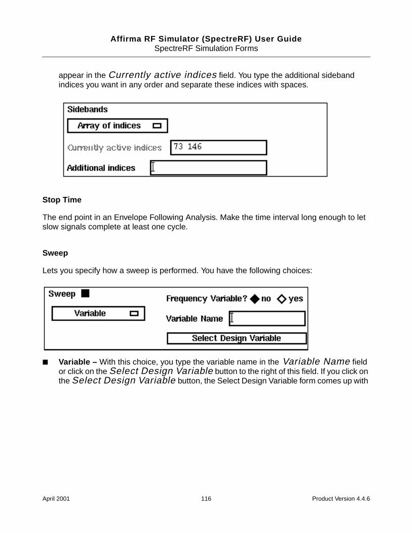
Affirma RF Simulator (SpectreRF) User GuideSpectreRF Simulation Forms
appear in the Currently active indices field. You type the additional sidebandindices you want in any order and separate these indices with spaces.
Stop Time
The end point in an Envelope Following Analysis. Make the time interval long enough to letslow signals complete at least one cycle.
Sweep
Lets you specify how a sweep is performed. You have the following choices:
Variable – With this choice, you type the variable name in the Variable Name fieldor click on the Select Design Variable button to the right of this field. If you click onthe Select Design Variable button, the Select Design Variable form comes up with
April 2001 116 Product Version 4.4.6
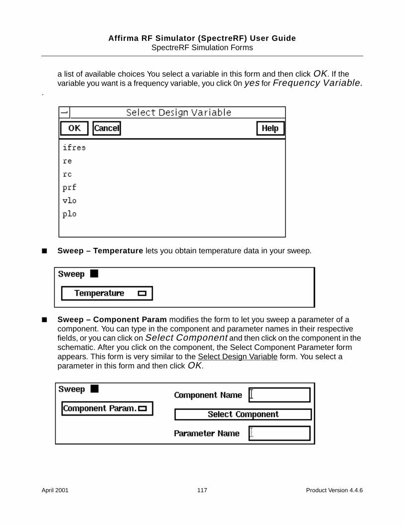
Affirma RF Simulator (SpectreRF) User GuideSpectreRF Simulation Forms
a list of available choices You select a variable in this form and then click OK. If thevariable you want is a frequency variable, you click 0n yes for Frequency Variable.
.
Sweep – Temperature lets you obtain temperature data in your sweep.
Sweep – Component Param modifies the form to let you sweep a parameter of acomponent. You can type in the component and parameter names in their respectivefields, or you can click on Select Component and then click on the component in theschematic. After you click on the component, the Select Component Parameter formappears. This form is very similar to the Select Design Variable form. You select aparameter in this form and then click OK.
April 2001 117 Product Version 4.4.6
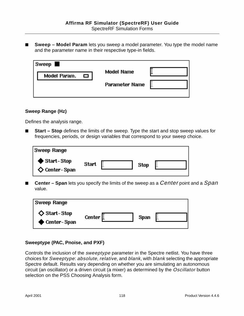
Affirma RF Simulator (SpectreRF) User GuideSpectreRF Simulation Forms
Sweep – Model Param lets you sweep a model parameter. You type the model nameand the parameter name in their respective type-in fields.
Sweep Range (Hz)
Defines the analysis range.
Start – Stop defines the limits of the sweep. Type the start and stop sweep values forfrequencies, periods, or design variables that correspond to your sweep choice.
Center – Span lets you specify the limits of the sweep as a Center point and a Spanvalue.
Sweeptype (PAC, Pnoise, and PXF)
Controls the inclusion of the sweeptype parameter in the Spectre netlist. You have threechoices for Sweeptype: absolute, relative, and blank, with blank selecting the appropriateSpectre default. Results vary depending on whether you are simulating an autonomouscircuit (an oscillator) or a driven circuit (a mixer) as determined by the Oscillator buttonselection on the PSS Choosing Analysis form.
April 2001 118 Product Version 4.4.6
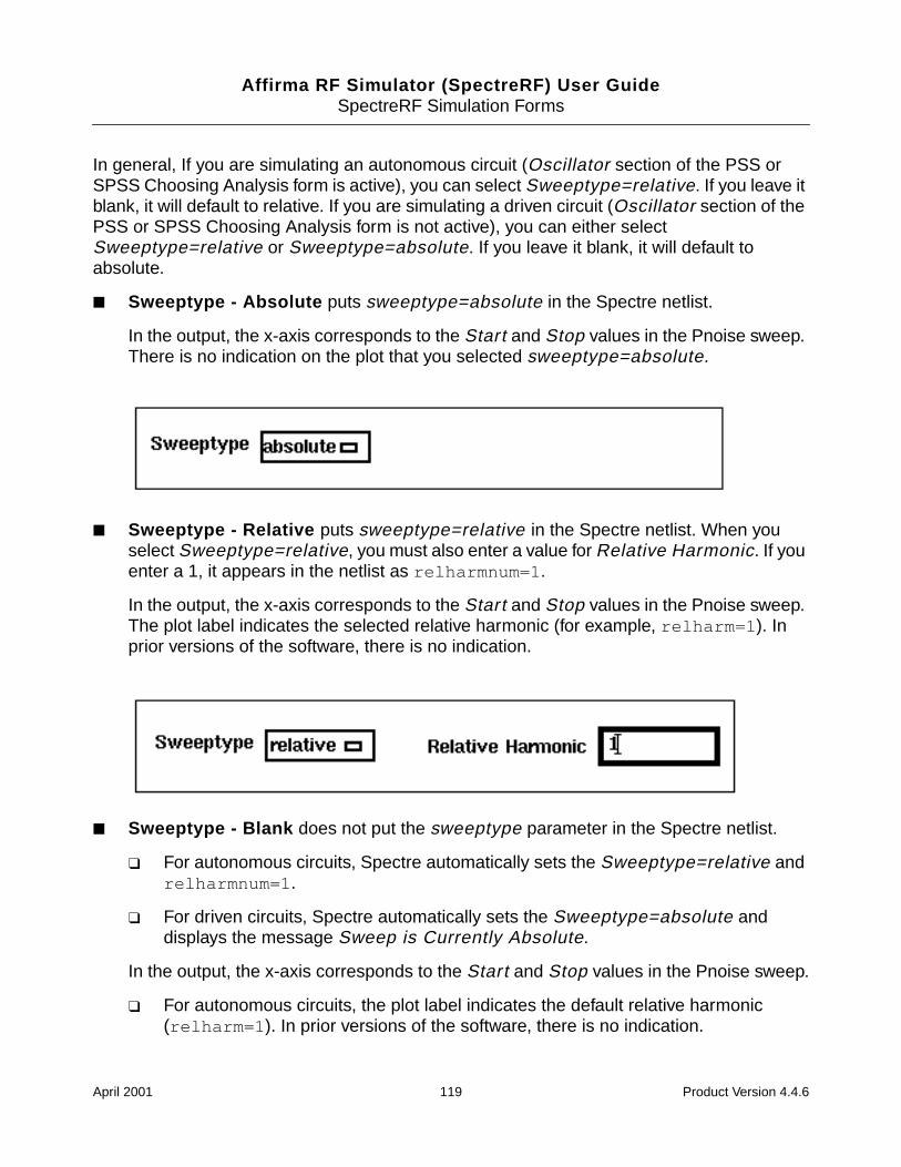
Affirma RF Simulator (SpectreRF) User GuideSpectreRF Simulation Forms
In general, If you are simulating an autonomous circuit (Oscillator section of the PSS orSPSS Choosing Analysis form is active), you can select Sweeptype=relative. If you leave itblank, it will default to relative. If you are simulating a driven circuit (Oscillator section of thePSS or SPSS Choosing Analysis form is not active), you can either selectSweeptype=relative or Sweeptype=absolute. If you leave it blank, it will default toabsolute.
Sweeptype - Absolute puts sweeptype=absolute in the Spectre netlist.
In the output, the x-axis corresponds to the Start and Stop values in the Pnoise sweep.There is no indication on the plot that you selected sweeptype=absolute.
Sweeptype - Relative puts sweeptype=relative in the Spectre netlist. When youselect Sweeptype=relative, you must also enter a value for Relative Harmonic. If youenter a 1, it appears in the netlist as relharmnum=1 .
In the output, the x-axis corresponds to the Start and Stop values in the Pnoise sweep.The plot label indicates the selected relative harmonic (for example, relharm=1 ). Inprior versions of the software, there is no indication.
Sweeptype - Blank does not put the sweeptype parameter in the Spectre netlist.
For autonomous circuits, Spectre automatically sets the Sweeptype=relative andrelharmnum=1 .
For driven circuits, Spectre automatically sets the Sweeptype=absolute anddisplays the message Sweep is Currently Absolute.
In the output, the x-axis corresponds to the Start and Stop values in the Pnoise sweep.
For autonomous circuits, the plot label indicates the default relative harmonic(relharm=1 ). In prior versions of the software, there is no indication.
April 2001 119 Product Version 4.4.6
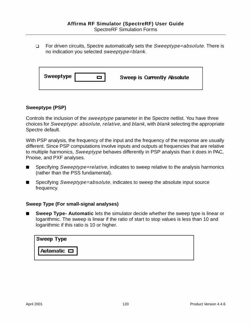
Affirma RF Simulator (SpectreRF) User GuideSpectreRF Simulation Forms
For driven circuits, Spectre automatically sets the Sweeptype=absolute. There isno indication you selected sweeptype=blank.
Sweeptype (PSP)
Controls the inclusion of the sweeptype parameter in the Spectre netlist. You have threechoices for Sweeptype: absolute, relative, and blank, with blank selecting the appropriateSpectre default.
With PSP analysis, the frequency of the input and the frequency of the response are usuallydifferent. Since PSP computations involve inputs and outputs at frequencies that are relativeto multiple harmonics, Sweeptype behaves differently in PSP analysis than it does in PAC,Pnoise, and PXF analyses.
Specifying Sweeptype=relative, indicates to sweep relative to the analysis harmonics(rather than the PSS fundamental).
Specifying Sweeptype=absolute, indicates to sweep the absolute input sourcefrequency.
Sweep Type (For small-signal analyses)
Sweep Type- Automatic lets the simulator decide whether the sweep type is linear orlogarithmic. The sweep is linear if the ratio of start to stop values is less than 10 andlogarithmic if this ratio is 10 or higher.
April 2001 120 Product Version 4.4.6
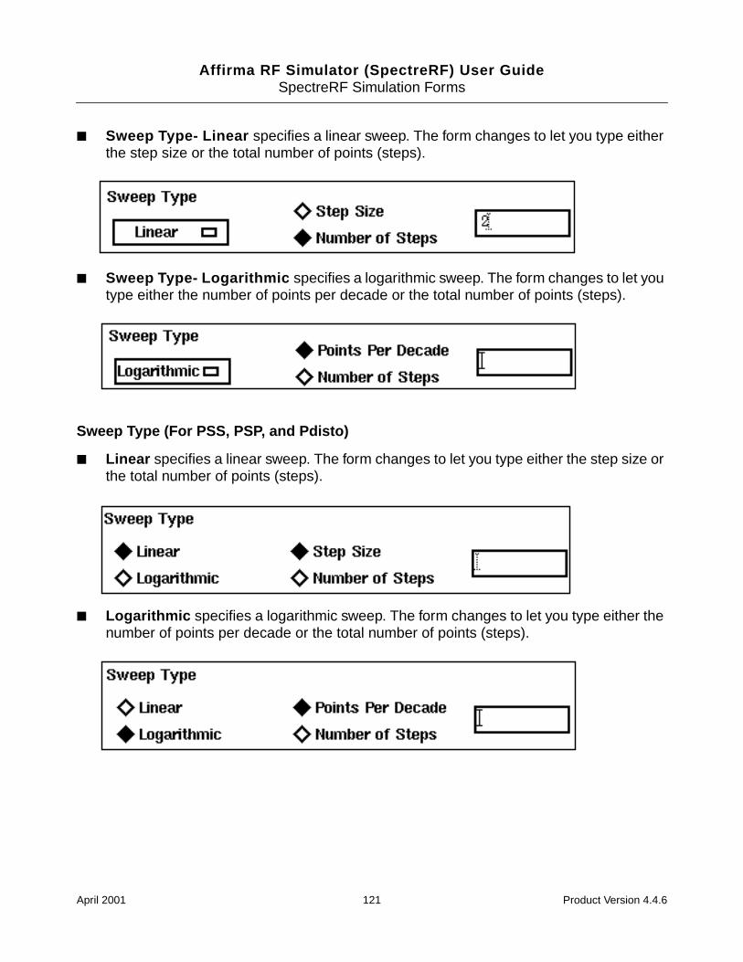
Affirma RF Simulator (SpectreRF) User GuideSpectreRF Simulation Forms
Sweep Type- Linear specifies a linear sweep. The form changes to let you type eitherthe step size or the total number of points (steps).
Sweep Type- Logarithmic specifies a logarithmic sweep. The form changes to let youtype either the number of points per decade or the total number of points (steps).
Sweep Type (For PSS, PSP, and Pdisto)
Linear specifies a linear sweep. The form changes to let you type either the step size orthe total number of points (steps).
Logarithmic specifies a logarithmic sweep. The form changes to let you type either thenumber of points per decade or the total number of points (steps).
April 2001 121 Product Version 4.4.6
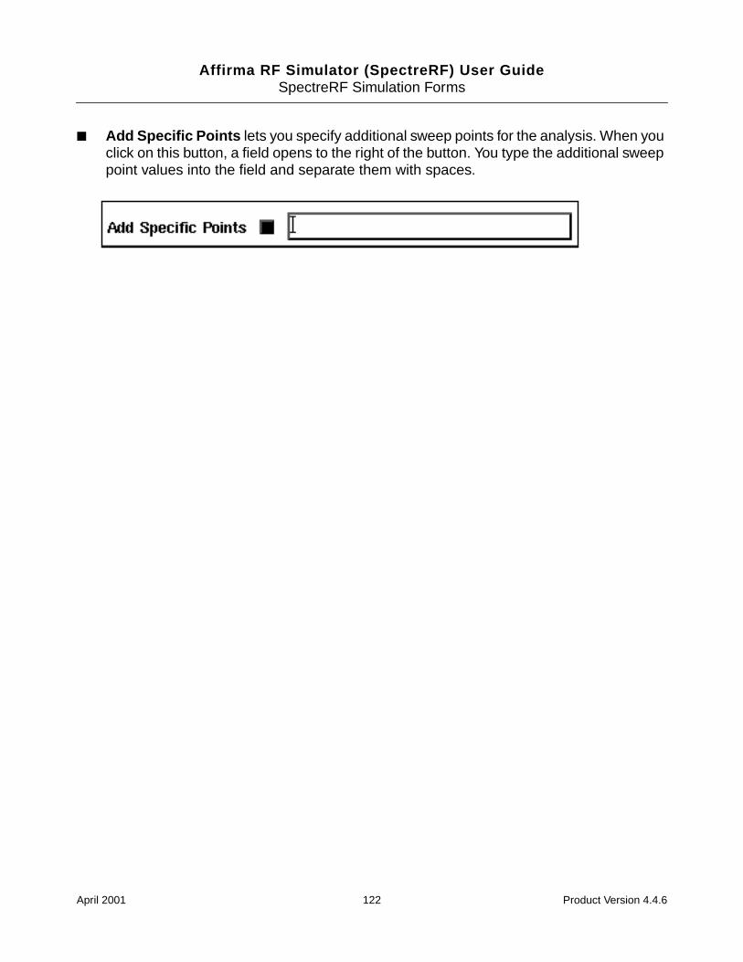
Affirma RF Simulator (SpectreRF) User GuideSpectreRF Simulation Forms
Add Specific Points lets you specify additional sweep points for the analysis. When youclick on this button, a field opens to the right of the button. You type the additional sweeppoint values into the field and separate them with spaces.
April 2001 122 Product Version 4.4.6

Affirma RF Simulator (SpectreRF) User GuideSpectreRF Simulation Forms
Options Forms
Clicking on an Options button on the Choosing Analysis form opens an Options form thatlets you specify simulation options for an analysis.
The Options button that appears when the Choosing Analyses form first opens letsyou specify options for the analysis you originally selected.
You see a second Options button in the expanded form if you specify data for anadditional small-signal analysis. This second Options button brings up an Options formfor the small-signal analysis.
Options that are not relevant for a particular analysis do not appear on its Options form.
The parameters you can specify on an options form are described in the following sections.
ACCURACY PARAMETERS
relref is the reference used for relative convergence criteria. Your accuracy default choicesets the default value.
pointlocal compares the relative errors in quantities at each node to that node alone.
alllocal compares the relative error at each node to the largest values ever found for thatnode.
sigglobal compares relative errors in each signal to the maximum value for all signals.
allglobal is the same as sigglobal except that it also compares the residues for eachnode to the historical maximum.
lteratio is the ratio the simulator uses to compute LTE tolerances from the Newton tolerance.The default value is based on the accuracy default.
steadyratio is the ratio the simulator uses to compute steady-state tolerances from the LTEtolerance. This parameter adjusts the maximum allowed mismatch in node voltages andcurrent branches during the steady-state period. The default is based on the accuracydefault.
maxacfreq is the maximum frequency used in a subsequent periodic small-signal analysis.This parameter automatically adjusts maxstep to reduce errors due to aliasing infrequency-domain results. The default is based on maxstep and harms values. Read“SpectreRF Theory” in the online documentation for more information about specifying thisparameter.
April 2001 123 Product Version 4.4.6
Affirma RF Simulator (SpectreRF) User GuideSpectreRF Simulation Forms
maxperiods is the maximum number of simulated periods allowed for the simulation toreach steady-state. Default is 20 .
Here are the default values controlled by the accuracy parameter settings:
finitediff lets you choose options for the finite difference method. Possible choices are yes,samegrid, or no.
For yes, PSS analysis improves the grid of time-steps and applies the finite differencemethod.
For samegrid, PSS analysis applies the finite difference method but keeps the grid oftime-steps used by the shooting method.
For no, PSS analysis does not use the finite difference method. If you reuse a previouslysaved PSS analysis result, fdtd is turned on automatically.
ANNOTATION PARAMETERS
stats tells the simulator to generate analysis statistics. Default is no.
annotate lets you specify what information is printed at the beginning of the output to identifythe results. Default is status.
CONVERGENCE PARAMETERS
readns lets you specify the name of a file that contains an estimate of the initial transientsolution. Enter the complete path to the file. No default.
cmin is the minimum capacitance from each node to ground. Default is 0.
tolerance is the relative tolerance for the linear solver when solving for convergence. Defaultis 10-9.
accuracy relref method steadyratio lteratio
liberal allglobal gear2 0.1 3.5
moderate sigglobal traponly 0.001 3.5
conservative alllocal gear2only 0.00001 10.0
April 2001 124 Product Version 4.4.6
Affirma RF Simulator (SpectreRF) User GuideSpectreRF Simulation Forms
gearorder is the order used for Gear-type interpolations. Default is 2 (second order).
solver
std specifies that Krylov subspaces not be used. Simulations with this setting are slowerbut more robust than simulations using the turbo setting. Use this setting if simulationwith turbo is unsuccessful.
exp currently has the same effect as std.
turbo specifies the use of Krylov subspaces and makes small-signal analyses run morequickly. However, it is less robust than std. This setting is the default.
oscsolver
std specifies that Krylov subspaces not be used. The setting is more robust than turbofor oscillator small-signal analyses, although the simulation is slower. Use this setting ifsimulation with turbo is unsuccessful.
turbo specifies the use of Krylov subspaces and makes oscillator small-signal analysesrun more quickly. However, it is less robust than std. This setting is the default.
INITIAL CONDITION PARAMETERS
ic specifies the methods used to set the initial condition. For an explanation of each of thesemethods, consult the “Spectre Reference manual. Default is all.
skipdc
yes omits the DC analysis from the transient analysis.
no includes a DC analysis with the transient analysis. This is the default.
waveless omits the initial DC analysis and fixes the independent source values to theirinitial values rather than their DC values.
rampup starts the independent source values at 0 and ramps them up to the initialvalues in the first 10% of the analysis interval.
autodc automatically selects either waveless or rampup, depending on whether youspecify a nonzero initial condition.
readic lets you specify the name of the file that contains the initial conditions.
April 2001 125 Product Version 4.4.6
Affirma RF Simulator (SpectreRF) User GuideSpectreRF Simulation Forms
INTEGRATION METHOD PARAMETERS
method specifies the integration method. Your accuracy default choice sets the default value.The possible settings are
euler is backward Euler.
trap is the backward Euler and trapezoidal methods.
traponly is the trapezoidal rule only.
gear2 is the backward Euler and second-order Gear methods.
gear2only is Gear’s second-order backward difference method only.
The trapezoidal rule is best when you want high accuracy, but it can exhibit point-to-pointringing, which you can control with tighter error tolerances. Euler and Gear work better withlooser tolerances for quick simulation, but they can make systems appear more stable thanthey actually are.
Use the gear_order option on the small-signal analyses Options form to set the order of aGear-type interpolation.
NEWTON PARAMETERS
maxiters is the maximum number of iterations per time step.
restart tells the simulator not to use the previous DC solution as an initial guess. Default isyes (means do not use).
envmaxiters lets you specify the maximum number of Newton iterations per envelope step.The default is 3.
OUTPUT PARAMETERS
save tells the simulator what signal to save You have the following choices:
selected saves only signals that you specifically request from the Outputs menu inthe Simulation window. It is the default setting.
lvlpub saves all signals that are normally useful up to nestlvl deep in the subcircuithierarchy. When you click on this button, the nestlvl type-in field below the lvlpubbutton activates to let you specify nestlvl.
April 2001 126 Product Version 4.4.6
Affirma RF Simulator (SpectreRF) User GuideSpectreRF Simulation Forms
lvl saves all signals that are up to nestlvl deep in the subcircuit hierarchy. When youclick on this button, the nestlvl field below the lvlpub button activates to let you specifynestlvl.
allpub saves all signals that are normally useful.
all saves all signals.
nestlvl is used with lvl and lvlpub. You type an integer that specifies the number oflevels in the hierarchy that you want to save signals.
oppoint specifies whether the simulator outputs the operating point information. You cansend the information to a rawfile, the logfile, or the screen. Default is no.
skipstart specifies when the simulator starts skipping output data. Default is starttime s(seconds).
skipstop specifies when the simulator stops skipping output data. Default is stoptime s(seconds).
skipcount specifies how many points to skip before saving a point. No default.
strobeperiod is the output strobe interval in seconds.
strobedelay is the delay (phase shift) between the skipstart time and the first strobe point.Default is 0.
compression directs the simulator to perform data compression on the output. Default isno.
stimuli specifies what PXF uses for inputs to the transfer functions.
sources specifies that the sources present in the circuit are used as the inputs to thetransfer functions.
nodes_and_terminals specifies that all possible transfer functions are computed.
freqaxis specifies what version of the frequency to plot the output against in spectral plots.
For the PAC and PXF analyses
absin is the absolute value of the input frequency.
in is the input frequency.
out is the output frequency.
For the PSP analysis
April 2001 127 Product Version 4.4.6
Affirma RF Simulator (SpectreRF) User GuideSpectreRF Simulation Forms
absin is the absolute value of the frequency swept at the input
in is the scattered frequency at the input
out is the scattered frequency at the output
compression performs data compression on the output.
outputperiod lets you specify the time-domain output period. The time-domain small-signalresponse is computed for the period specified, rounded to the nearest integer multiple of thePSS analysis period.
outputtype lets you specify the output type for Envelope Following Analysis. Possible valuesare both, envelope, or spectrum. The default is both.
saveallsidebands lets you save all sidebands.
SIMULATION INTERVAL PARAMETERS
tstart is the start time you specify for transient analysis. It can be negative or positive. Defaultis 0.
start lets you specify the start time for the Envelope Following Analysis.
outputstart lets you specify the timepoint when the simulator starts to save output.
SIMULATION BANDWIDTH PARAMETERS
modulationbw lets you specify the modulation bandwidth.
STATE FILE PARAMETERS
write lets you specify the name of the file to which the SpectreRF simulation writes the initialtransient solution.
writefinal lets you specify the name of the file to which the SpectreRF simulation writes thefinal transient solution.
swapfile is a temporary file that holds steady-state information. If you enter a filename, theSpectre circuit simulator stores the operating point in that file rather than in virtual memory.Use this option if you receive a warning about not having enough memory to complete theanalysis. Enter the complete path to the file.
April 2001 128 Product Version 4.4.6
Affirma RF Simulator (SpectreRF) User GuideSpectreRF Simulation Forms
writepss specifies the file to which the steady-state solution is written. Small-signal analysescan read the steady-state solution from this file so rerunning the PSS analysis isunnecessary.
readpss specifies the file from which the steady-state solution is read. Small-signal analysescan read the steady-state solution from this file so rerunning the PSS analysis isunnecessary.
TIME STEP PARAMETERS
step is the smallest simulator time step used to improve the look of the results. Default is0.001 x fundamental period seconds.
maxstep is the largest allowable time step. The default is set by the accuracy default.
liberal = 0.1/max AC frequency
moderate = 2 x liberal
conservative = 4 x liberal
maxenvstep specifies the maximum outer envelope size. The default is derived from theerrpreset setting.
April 2001 129 Product Version 4.4.6
Affirma RF Simulator (SpectreRF) User GuideSpectreRF Simulation Forms
Results Forms
1st Order Harmonic
See First-Order Harmonic
2nd-7th Order Harmonic
See Nth Order Harmonic
Add To Outputs
Adds the expression plotted in the Direct Plot window to the Outputs list in the Simulationwindow.
Analysis Type
Selects which analysis you can plot the results from. If you include a small-signal analysis, ithas its own button. Clicking on a different analysis button changes the appearance of theResults form.
Circuit Input Power lets you choose between Single Point and an appropriate sweep. Ifyou choose Single Point, the Input Power Value (dBm) field appears, and youmust type a value into it. If you choose a sweep, the Extrapolation Point field appears,and you can type a value. Placing a value in the Extrapolation Point field is optional.
Close Contours
Is used in plotting power and reflection contours. When you select this option, the plotappears as a closed figure. The default is to leave the two most distant points in the plotunconnected.
Extrapolation Point
The optional Extrapolation Point field lets you specify the value of the design variablefrom which the straight line approximations of first- and third-order harmonics areproduced. If you do not specify a value, the default value is the smallest X-axis sweep value.
April 2001 130 Product Version 4.4.6
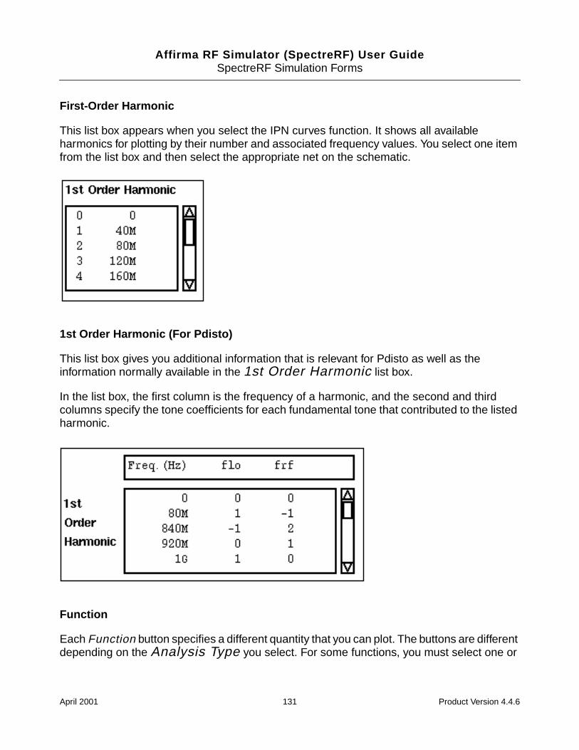
Affirma RF Simulator (SpectreRF) User GuideSpectreRF Simulation Forms
First-Order Harmonic
This list box appears when you select the IPN curves function. It shows all availableharmonics for plotting by their number and associated frequency values. You select one itemfrom the list box and then select the appropriate net on the schematic.
1st Order Harmonic (For Pdisto)
This list box gives you additional information that is relevant for Pdisto as well as theinformation normally available in the 1st Order Harmonic list box.
In the list box, the first column is the frequency of a harmonic, and the second and thirdcolumns specify the tone coefficients for each fundamental tone that contributed to the listedharmonic.
Function
Each Function button specifies a different quantity that you can plot. The buttons are differentdepending on the Analysis Type you select. For some functions, you must select one or
April 2001 131 Product Version 4.4.6
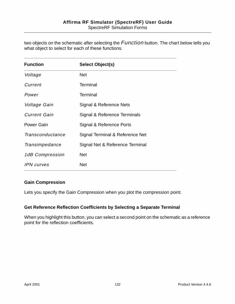
Affirma RF Simulator (SpectreRF) User GuideSpectreRF Simulation Forms
two objects on the schematic after selecting the Function button. The chart below tells youwhat object to select for each of these functions.
Gain Compression
Lets you specify the Gain Compression when you plot the compression point.
Get Reference Reflection Coefficients by Selecting a Separate Terminal
When you highlight this button, you can select a second point on the schematic as a referencepoint for the reflection coefficients.
Function Select Object(s)
Voltage Net
Current Terminal
Power Terminal
Voltage Gain Signal & Reference Nets
Current Gain Signal & Reference Terminals
Power Gain Signal & Reference Ports
Transconductance Signal Terminal & Reference Net
Transimpedance Signal Net & Reference Terminal
1dB Compression Net
IPN curves Net
April 2001 132 Product Version 4.4.6
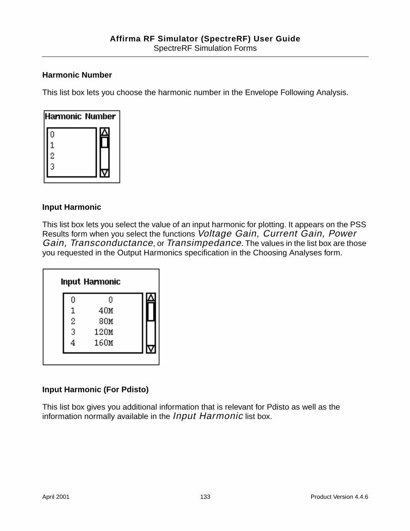
Affirma RF Simulator (SpectreRF) User GuideSpectreRF Simulation Forms
Harmonic Number
This list box lets you choose the harmonic number in the Envelope Following Analysis.
Input Harmonic
This list box lets you select the value of an input harmonic for plotting. It appears on the PSSResults form when you select the functions Voltage Gain, Current Gain, PowerGain, Transconductance, or Transimpedance. The values in the list box are thoseyou requested in the Output Harmonics specification in the Choosing Analyses form.
Input Harmonic (For Pdisto)
This list box gives you additional information that is relevant for Pdisto as well as theinformation normally available in the Input Harmonic list box.
April 2001 133 Product Version 4.4.6
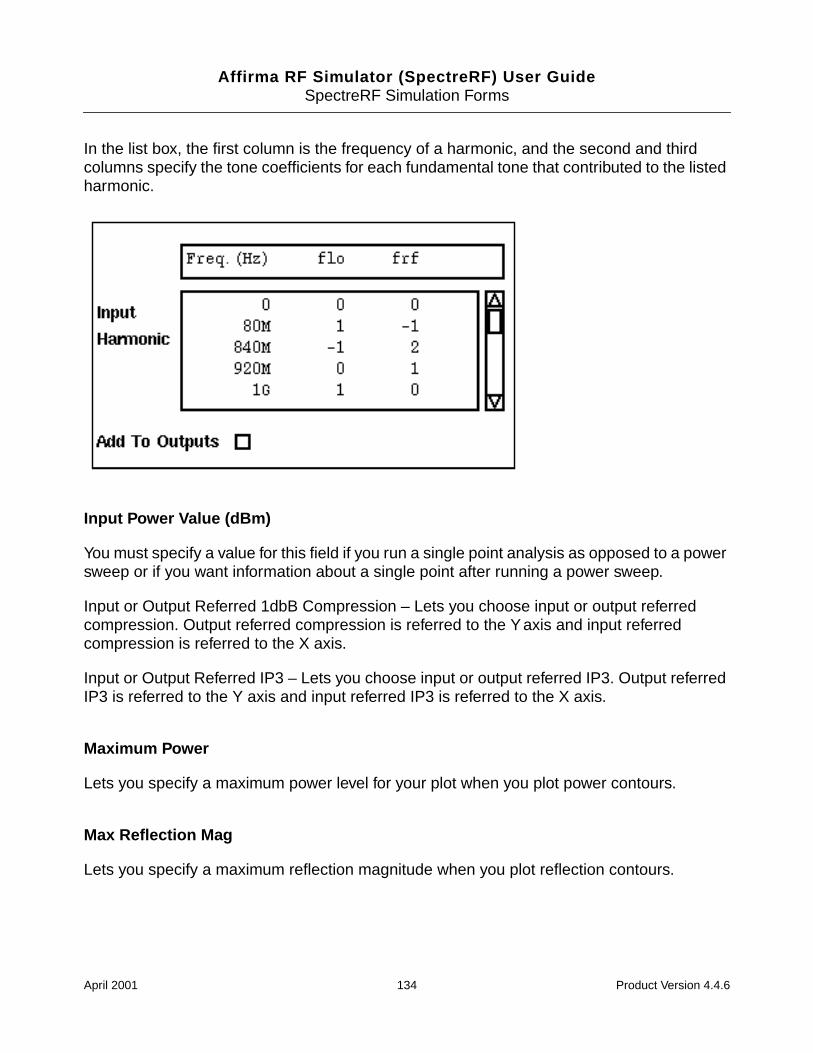
Affirma RF Simulator (SpectreRF) User GuideSpectreRF Simulation Forms
In the list box, the first column is the frequency of a harmonic, and the second and thirdcolumns specify the tone coefficients for each fundamental tone that contributed to the listedharmonic.
Input Power Value (dBm)
You must specify a value for this field if you run a single point analysis as opposed to a powersweep or if you want information about a single point after running a power sweep.
Input or Output Referred 1dbB Compression – Lets you choose input or output referredcompression. Output referred compression is referred to the Yaxis and input referredcompression is referred to the X axis.
Input or Output Referred IP3 – Lets you choose input or output referred IP3. Output referredIP3 is referred to the Y axis and input referred IP3 is referred to the X axis.
Maximum Power
Lets you specify a maximum power level for your plot when you plot power contours.
Max Reflection Mag
Lets you specify a maximum reflection magnitude when you plot reflection contours.
April 2001 134 Product Version 4.4.6

Affirma RF Simulator (SpectreRF) User GuideSpectreRF Simulation Forms
Minimum Power
Lets you specify a minimum power level for your plot when you plot power contours.
Min Reflection Mag
Lets you specify a minimum reflection magnitude when you plot reflection contours.
Modifier
This function sets the units of the y axis.
Magnitude is the raw value, in volts, amps, or no units at all.
Phase sets the Y axis to degrees.
dB20 sets the Y axis to decibels with tick marks every 20 dB.
dBm sets the Y axis to dB 10 plus 30.
dB10 sets the Y axis to decibels with tick marks every 10 dB.
Real and Imaginary restrict plots to only the real or imaginary range of the curve.
Number of Contours
Lets you specify the number of power or reflection contours that you want to plot.
Nth Order Harmonic
This list box appears when you select the IPN curves function. It shows all the harmonicsavailable for plotting by their number and associated frequency values. You select one itemfrom the list box and then select the appropriate net on the schematic.
April 2001 135 Product Version 4.4.6
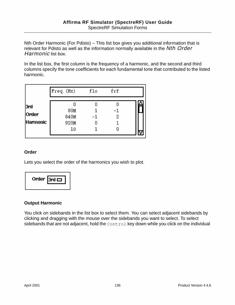
Affirma RF Simulator (SpectreRF) User GuideSpectreRF Simulation Forms
Nth Order Harmonic (For Pdisto) – This list box gives you additional information that isrelevant for Pdisto as well as the information normally available in the Nth OrderHarmonic list box.
In the list box, the first column is the frequency of a harmonic, and the second and thirdcolumns specify the tone coefficients for each fundamental tone that contributed to the listedharmonic.
Order
Lets you select the order of the harmonics you wish to plot.
Output Harmonic
You click on sidebands in the list box to select them. You can select adjacent sidebands byclicking and dragging with the mouse over the sidebands you want to select. To selectsidebands that are not adjacent, hold the Control key down while you click on the individual
April 2001 136 Product Version 4.4.6
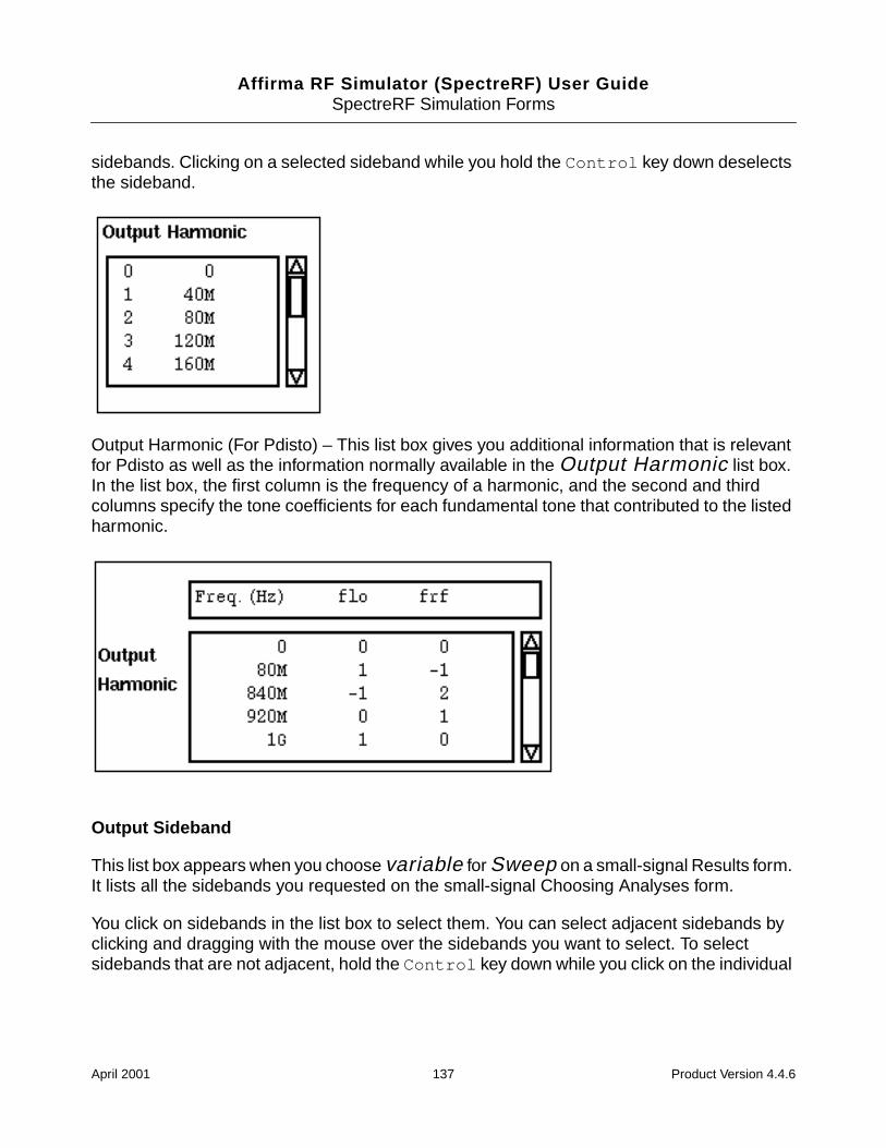
Affirma RF Simulator (SpectreRF) User GuideSpectreRF Simulation Forms
sidebands. Clicking on a selected sideband while you hold the Control key down deselectsthe sideband.
Output Harmonic (For Pdisto) – This list box gives you additional information that is relevantfor Pdisto as well as the information normally available in the Output Harmonic list box.In the list box, the first column is the frequency of a harmonic, and the second and thirdcolumns specify the tone coefficients for each fundamental tone that contributed to the listedharmonic.
Output Sideband
This list box appears when you choose variable for Sweep on a small-signal Results form.It lists all the sidebands you requested on the small-signal Choosing Analyses form.
You click on sidebands in the list box to select them. You can select adjacent sidebands byclicking and dragging with the mouse over the sidebands you want to select. To selectsidebands that are not adjacent, hold the Control key down while you click on the individual
April 2001 137 Product Version 4.4.6
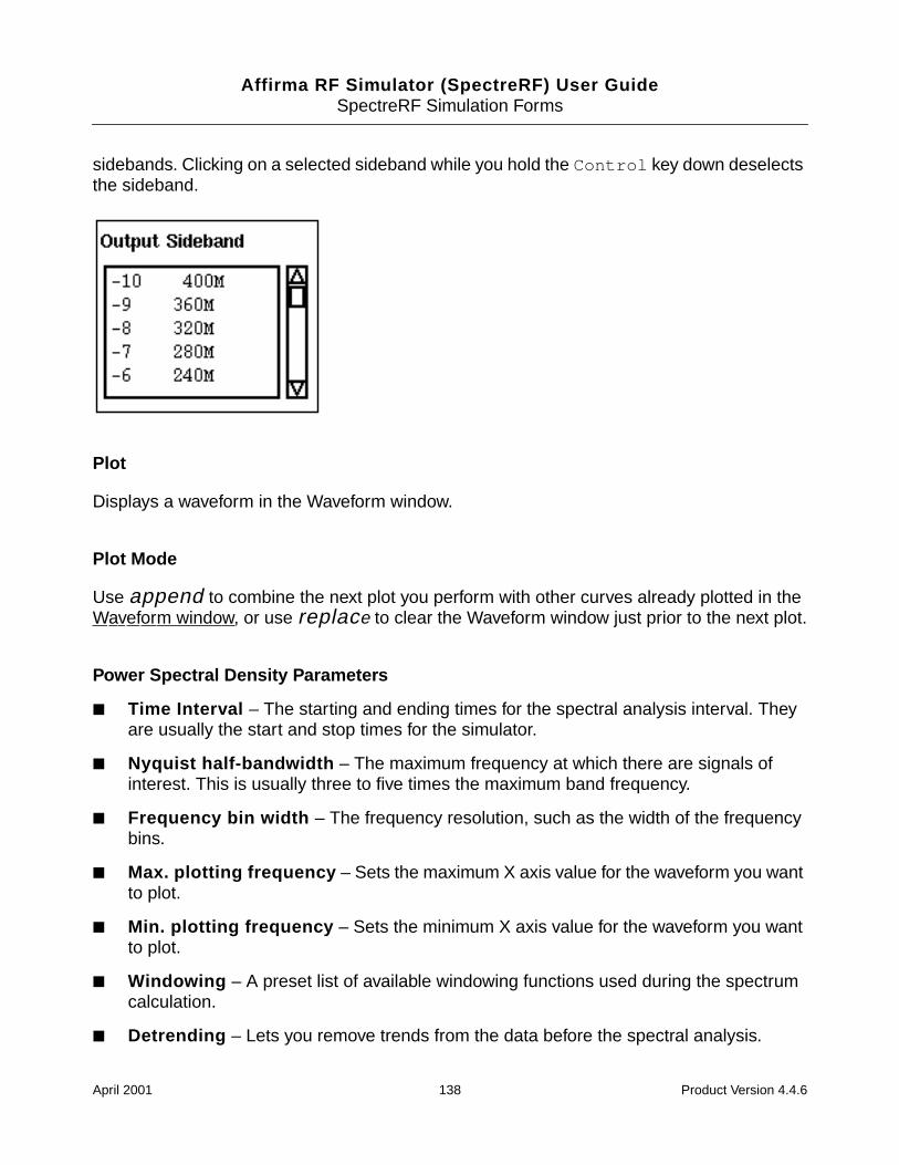
Affirma RF Simulator (SpectreRF) User GuideSpectreRF Simulation Forms
sidebands. Clicking on a selected sideband while you hold the Control key down deselectsthe sideband.
Plot
Displays a waveform in the Waveform window.
Plot Mode
Use append to combine the next plot you perform with other curves already plotted in theWaveform window, or use replace to clear the Waveform window just prior to the next plot.
Power Spectral Density Parameters
Time Interval – The starting and ending times for the spectral analysis interval. Theyare usually the start and stop times for the simulator.
Nyquist half-bandwidth – The maximum frequency at which there are signals ofinterest. This is usually three to five times the maximum band frequency.
Frequency bin width – The frequency resolution, such as the width of the frequencybins.
Max. plotting frequency – Sets the maximum X axis value for the waveform you wantto plot.
Min. plotting frequency – Sets the minimum X axis value for the waveform you wantto plot.
Windowing – A preset list of available windowing functions used during the spectrumcalculation.
Detrending – Lets you remove trends from the data before the spectral analysis.
April 2001 138 Product Version 4.4.6

Affirma RF Simulator (SpectreRF) User GuideSpectreRF Simulation Forms
Reference Resistance
Lets you specify the resistance of the port adapter when you plot power or reflection contours.
Sweep
spectrum, sideband, and frequency set the X axis of the plot to frequency
time sets the X axis of the plot to seconds
variable sets the X axis to the value of a design variable.
Variable Value
The PSS and Pdisto Results forms display this list of sweep values that you can specify fora specific variable, temperature, component parameter, or model parameter. The range ofvalues is determined by your Sweep Range specification and the number of values by yourSweep Type specification in the Choosing Analyses form. In the sample figure, whichshows the PSS version, the values are listed for the design variable prf.The Pdisto versionof the form is formatted slightly differently but gives the same information.
April 2001 139 Product Version 4.4.6
Affirma RF Simulator (SpectreRF) User Guide
3Setting Up for the Examples
This chapter tells you how to set up your software so you can follow the instructions and runthe examples in the chapters about simulating specific components.
Setting Up the Software
Before you perform the SpectreRF simulator analyses, you must set up the component filesand start the Cadence® software.
Copying the SpectreRF Simulator Examples
Copy the rfExamples library into your account so that you can edit the sample design.
The library is located at
<CDSHOME>/tools/dfII/samples/artist/rfExamples
where CDSHOME is the installation directory for your Cadence software.
Setting Up the Cadence Libraries
The Cadence Libraries are defined in the UNIX text file cds.lib . You can edit this file in aUNIX shell window or by using the Library Path Editor while running the Cadence software.
Using a UNIX Shell Window
To set up the libraries in a UNIX shell window, use the following procedure:
1. In a UNIX shell window, open the cds.lib file for editing using vi, emacs or a similartext editor.
The cds.lib file is in your installation directory.
April 2001 140 Product Version 4.4.6
Affirma RF Simulator (SpectreRF) User GuideSetting Up for the Examples
2. In the cds.lib file, specify definitions for the basic , analogLib , sample , andspectreSModels libraries. In addition, define a user library where the sample circuitscan be tested. The definitions in the cds.lib file look like the following:
DEFINE rf_test my_dir / rf_testDEFINE basic < CDSHOME>/tools/dfII/etc/cdslib/basicDEFINE analogLib < CDSHOME>/tools/dfII/etc/cdslib/artist/analogLibDEFINE sample < CDSHOME>/tools/dfII/samples/cdslib/sampleDEFINE spectreSModels < CDSHOME>/tools/dfII/samples/artist/
spectreSModels
You can label your test library any name you choose. This example assumes that youhave called the library rf_test . The name my_dir represents the directory intowhich you copied the design library.
You must use the names basic , sample , analogLib, and spectreSModels .You cannot rename those four libraries.
Using the Library Path Editor
To access the Library Path Editor, use the following procedure.
1. In a UNIX window, type icms to start the Cadence software.
The Command Interpreter Window (CIW) appears.
2. In the CIW, choose Tools – Library Path Editor.
The Library Path Editor form appears.
April 2001 141 Product Version 4.4.6
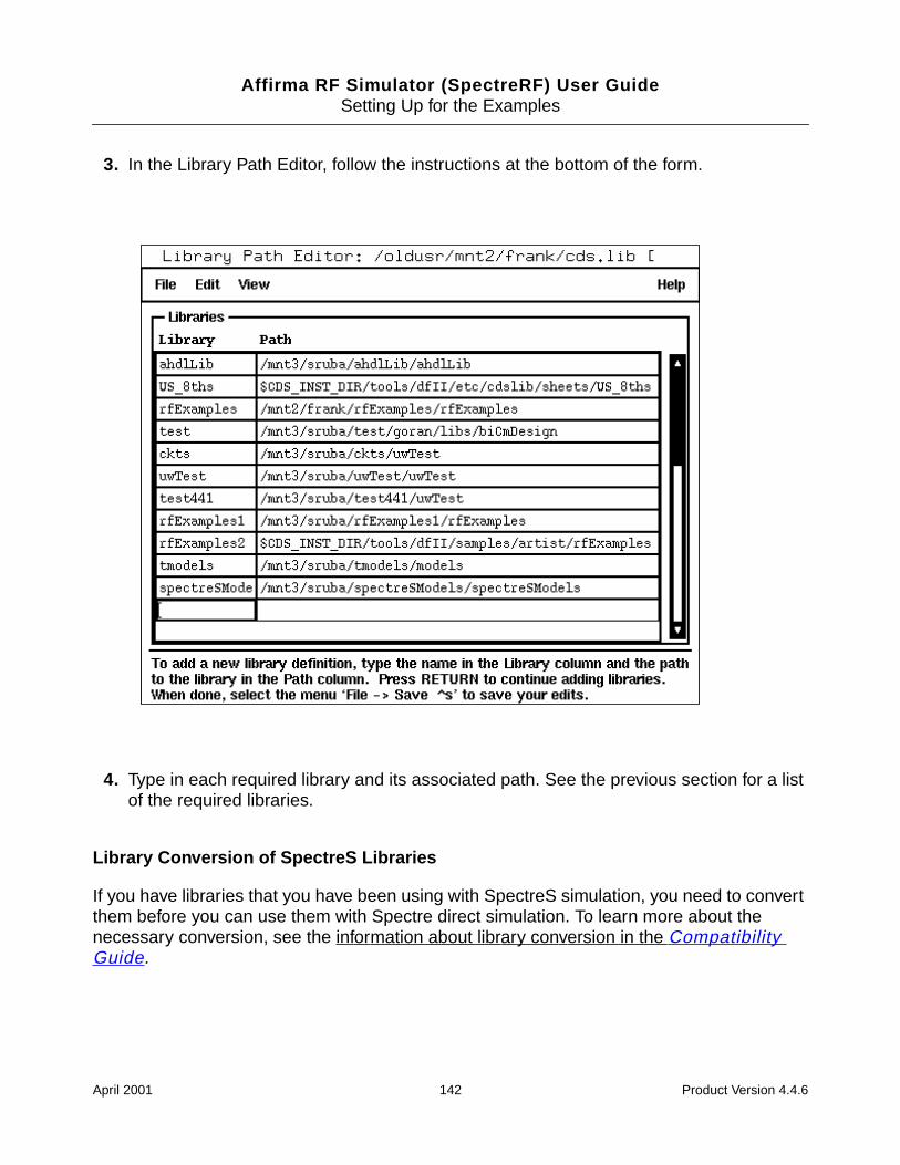
Affirma RF Simulator (SpectreRF) User GuideSetting Up for the Examples
3. In the Library Path Editor, follow the instructions at the bottom of the form.
4. Type in each required library and its associated path. See the previous section for a listof the required libraries.
Library Conversion of SpectreS Libraries
If you have libraries that you have been using with SpectreS simulation, you need to convertthem before you can use them with Spectre direct simulation. To learn more about thenecessary conversion, see the information about library conversion in the CompatibilityGuide.
April 2001 142 Product Version 4.4.6
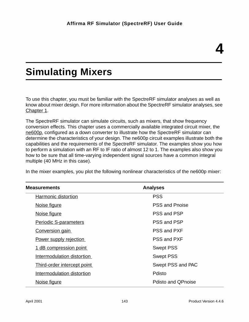
Affirma RF Simulator (SpectreRF) User Guide
4Simulating Mixers
To use this chapter, you must be familiar with the SpectreRF simulator analyses as well asknow about mixer design. For more information about the SpectreRF simulator analyses, seeChapter 1.
The SpectreRF simulator can simulate circuits, such as mixers, that show frequencyconversion effects. This chapter uses a commercially available integrated circuit mixer, thene600p, configured as a down converter to illustrate how the SpectreRF simulator candetermine the characteristics of your design. The ne600p circuit examples illustrate both thecapabilities and the requirements of the SpectreRF simulator. The examples show you howto perform a simulation with an RF to IF ratio of almost 12 to 1. The examples also show youhow to be sure that all time-varying independent signal sources have a common integralmultiple (40 MHz in this case).
In the mixer examples, you plot the following nonlinear characteristics of the ne600p mixer:
Measurements Analyses
Harmonic distortion PSS
Noise figure PSS and Pnoise
Noise figure PSS and PSP
Periodic S-parameters PSS and PSP
Conversion gain PSS and PXF
Power supply rejection PSS and PXF
1 dB compression point Swept PSS
Intermodulation distortion Swept PSS
Third-order intercept point Swept PSS and PAC
Intermodulation distortion Pdisto
Noise figure Pdisto and QPnoise
April 2001 143 Product Version 4.4.6
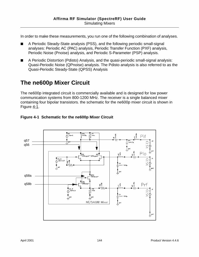
Affirma RF Simulator (SpectreRF) User GuideSimulating Mixers
In order to make these measurements, you run one of the following combination of analyses.
A Periodic Steady-State analysis (PSS), and the following periodic small-signalanalyses: Periodic AC (PAC) analysis, Periodic Transfer Function (PXF) analysis,Periodic Noise (Pnoise) analysis, and Periodic S-Parameter (PSP) analysis.
A Periodic Distortion (Pdisto) Analysis, and the quasi-periodic small-signal analysis:Quasi-Periodic Noise (QPnoise) analysis. The Pdisto analysis is also referred to as theQuasi-Periodic Steady-State (QPSS) Analysis
The ne600p Mixer Circuit
The ne600p integrated circuit is commercially available and is designed for low powercommunication systems from 800-1200 MHz. The receiver is a single balanced mixercontaining four bipolar transistors. the schematic for the ne600p mixer circuit is shown inFigure 4-1.
Figure 4-1 Schematic for the ne600p Mixer Circuit
q57q56
q58b
q58a
April 2001 144 Product Version 4.4.6
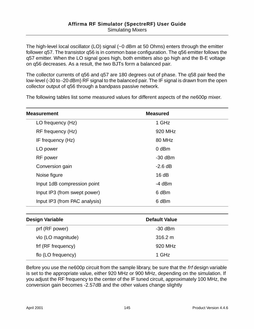
Affirma RF Simulator (SpectreRF) User GuideSimulating Mixers
The high-level local oscillator (LO) signal (~0 dBm at 50 Ohms) enters through the emitterfollower q57. The transistor q56 is in common base configuration. The q56 emitter follows theq57 emitter. When the LO signal goes high, both emitters also go high and the B-E voltageon q56 decreases. As a result, the two BJTs form a balanced pair.
The collector currents of q56 and q57 are 180 degrees out of phase. The q58 pair feed thelow-level (-30 to -20 dBm) RF signal to the balanced pair. The IF signal is drawn from the opencollector output of q56 through a bandpass passive network.
The following tables list some measured values for different aspects of the ne600p mixer.
Before you use the ne600p circuit from the sample library, be sure that the frf design variableis set to the appropriate value, either 920 MHz or 900 MHz, depending on the simulation. Ifyou adjust the RF frequency to the center of the IF tuned circuit, approximately 100 MHz, theconversion gain becomes -2.57dB and the other values change slightly
Measurement Measured
LO frequency (Hz) 1 GHz
RF frequency (Hz) 920 MHz
IF frequency (Hz) 80 MHz
LO power 0 dBm
RF power -30 dBm
Conversion gain -2.6 dB
Noise figure 16 dB
Input 1dB compression point -4 dBm
Input IP3 (from swept power) 6 dBm
Input IP3 (from PAC analysis) 6 dBm
Design Variable Default Value
prf (RF power) -30 dBm
vlo (LO magnitude) 316.2 m
frf (RF frequency) 920 MHz
flo (LO frequency) 1 GHz
April 2001 145 Product Version 4.4.6
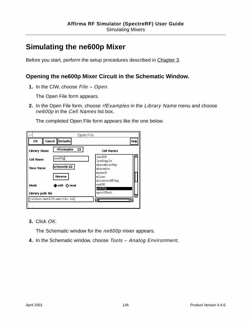
Affirma RF Simulator (SpectreRF) User GuideSimulating Mixers
Simulating the ne600p Mixer
Before you start, perform the setup procedures described in Chapter 3.
Opening the ne600p Mixer Circuit in the Schematic Window.
1. In the CIW, choose File – Open.
The Open File form appears.
2. In the Open File form, choose rfExamples in the Library Name menu and choosene600p in the Cell Names list box.
The completed Open File form appears like the one below.
3. Click OK.
The Schematic window for the ne600p mixer appears.
4. In the Schematic window, choose Tools – Analog Environment.
April 2001 146 Product Version 4.4.6
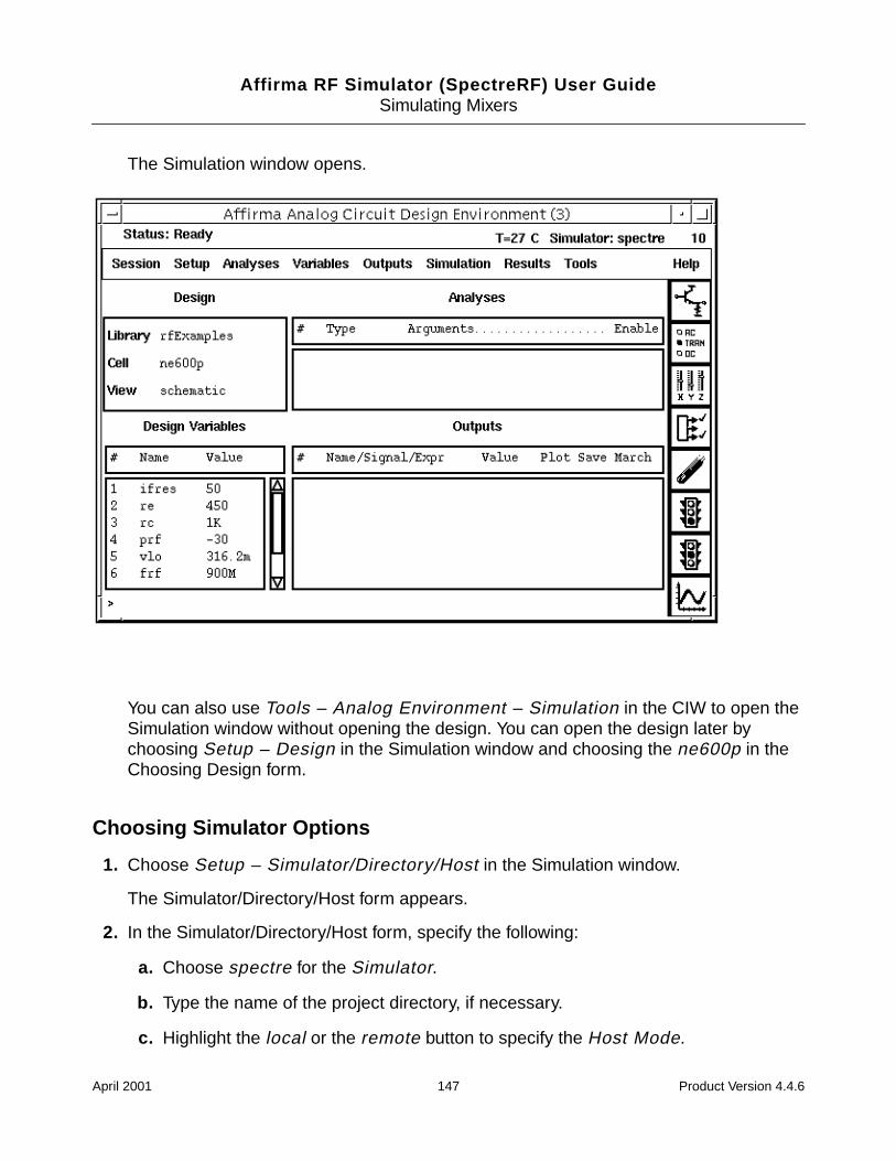
Affirma RF Simulator (SpectreRF) User GuideSimulating Mixers
The Simulation window opens.
You can also use Tools – Analog Environment – Simulation in the CIW to open theSimulation window without opening the design. You can open the design later bychoosing Setup – Design in the Simulation window and choosing the ne600p in theChoosing Design form.
Choosing Simulator Options
1. Choose Setup – Simulator/Directory/Host in the Simulation window.
The Simulator/Directory/Host form appears.
2. In the Simulator/Directory/Host form, specify the following:
a. Choose spectre for the Simulator.
b. Type the name of the project directory, if necessary.
c. Highlight the local or the remote button to specify the Host Mode.
April 2001 147 Product Version 4.4.6
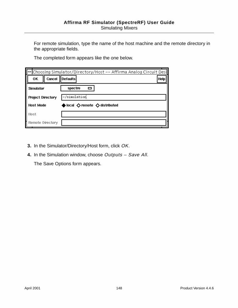
Affirma RF Simulator (SpectreRF) User GuideSimulating Mixers
For remote simulation, type the name of the host machine and the remote directory inthe appropriate fields.
The completed form appears like the one below.
3. In the Simulator/Directory/Host form, click OK.
4. In the Simulation window, choose Outputs – Save All.
The Save Options form appears.
April 2001 148 Product Version 4.4.6
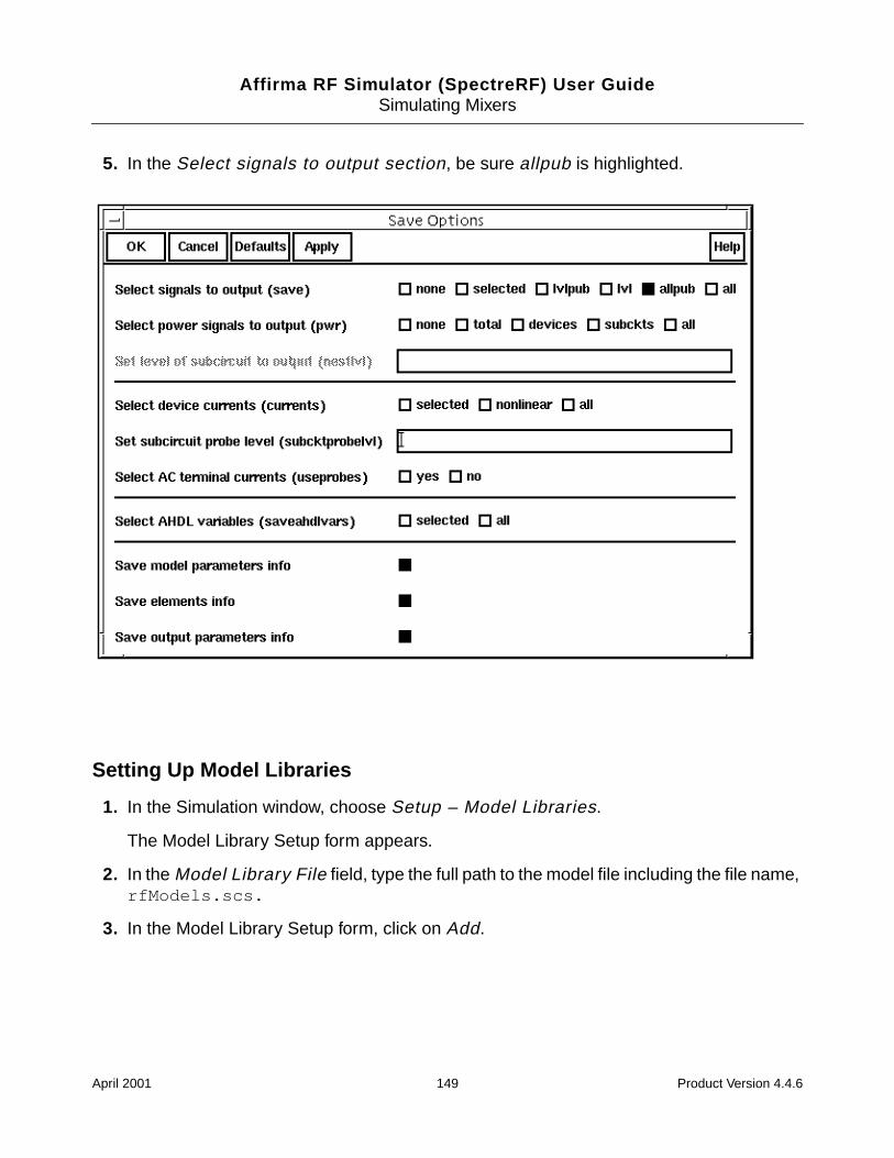
Affirma RF Simulator (SpectreRF) User GuideSimulating Mixers
5. In the Select signals to output section, be sure allpub is highlighted.
Setting Up Model Libraries
1. In the Simulation window, choose Setup – Model Libraries.
The Model Library Setup form appears.
2. In the Model Library File field, type the full path to the model file including the file name,rfModels.scs.
3. In the Model Library Setup form, click on Add.
April 2001 149 Product Version 4.4.6
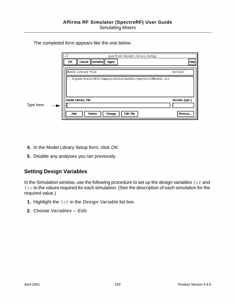
Affirma RF Simulator (SpectreRF) User GuideSimulating Mixers
The completed form appears like the one below.
4. In the Model Library Setup form, click OK.
5. Disable any analyses you ran previously.
Setting Design Variables
In the Simulation window, use the following procedure to set up the design variables frf andflo to the values required for each simulation. (See the description of each simulation for therequired value.)
1. Highlight the frf in the Design Variable list box.
2. Choose Variables – Edit.
Type here.
April 2001 150 Product Version 4.4.6
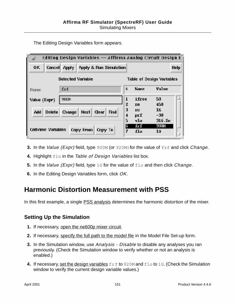
Affirma RF Simulator (SpectreRF) User GuideSimulating Mixers
The Editing Design Variables form appears.
3. In the Value (Expr) field, type 900M (or 920M) for the value of frf and click Change.
4. Highlight flo in the Table of Design Variables list box.
5. In the Value (Expr) field, type 1G for the value of flo and then click Change.
6. In the Editing Design Variables form, click OK.
Harmonic Distortion Measurement with PSS
In this first example, a single PSS analysis determines the harmonic distortion of the mixer.
Setting Up the Simulation
1. If necessary, open the ne600p mixer circuit.
2. If necessary, specify the full path to the model file in the Model File Set-up form.
3. In the Simulation window, use Analysis - Disable to disable any analyses you ranpreviously. (Check the Simulation window to verify whether or not an analysis isenabled.)
4. If necessary, set the design variables frf to 920Mand flo to 1G. (Check the Simulationwindow to verify the current design variable values.)
April 2001 151 Product Version 4.4.6
Affirma RF Simulator (SpectreRF) User GuideSimulating Mixers
Editing the Schematic
A critical part of this analysis is the correct use of the programmable voltage sources in thene600p circuit. The RF voltage source is based on the port sample component. You mustchange the behavior of this component for each analysis.
1. Choose Edit – Properties – Objects in the Schematic window.
The Edit Object Properties form appears. You use this form to change the list of CDF(component description format) properties for the rf voltage source and modify theschematic for this simulation.
2. In the Schematic window, click on the rf voltage source.
The Edit Object Properties form changes to display information for the voltage source.
3. In the Edit Object Properties form, be sure that sine is specified as the Source type.
April 2001 152 Product Version 4.4.6
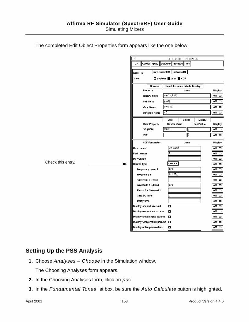
Affirma RF Simulator (SpectreRF) User GuideSimulating Mixers
The completed Edit Object Properties form appears like the one below:
Setting Up the PSS Analysis
1. Choose Analyses – Choose in the Simulation window.
The Choosing Analyses form appears.
2. In the Choosing Analyses form, click on pss.
3. In the Fundamental Tones list box, be sure the Auto Calculate button is highlighted.
Check this entry.
April 2001 153 Product Version 4.4.6
Affirma RF Simulator (SpectreRF) User GuideSimulating Mixers
The Beat Frequency is now displayed. The 40 Mvalue is the minimum period for whichboth RF at 920 MHz and the LO at 1 GHz are periodic (or for which RF and LO areinteger multiples of the fundamental frequency).
The Beat Frequency button is highlighted by default.
In the Choosing Analyses form, perform the following steps:
1. In the Output harmonics cyclic field, choose Number of harmonics for the Outputharmonics choice and type 30 for the number of harmonics in the field.
This entry expands the plotted frequency range to include the areas of interest aroundboth 40 MHzand 1 GHz. (30 x 40 MHzequals 1.2 GHz , or 0 to 1.2 GHz , and includesall important frequencies.)
2. Highlight conservative for the Accuracy Defaults (errpreset) setting.
April 2001 154 Product Version 4.4.6
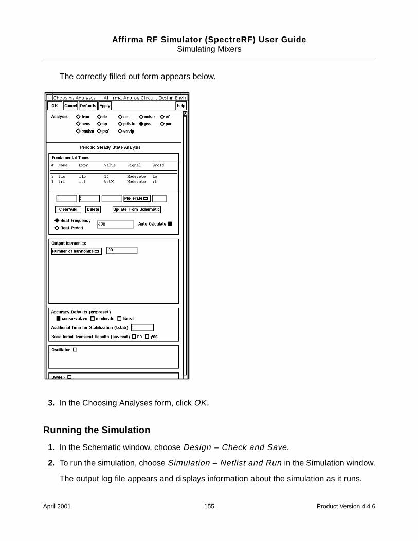
Affirma RF Simulator (SpectreRF) User GuideSimulating Mixers
The correctly filled out form appears below.
3. In the Choosing Analyses form, click OK.
Running the Simulation
1. In the Schematic window, choose Design – Check and Save.
2. To run the simulation, choose Simulation – Netlist and Run in the Simulation window.
The output log file appears and displays information about the simulation as it runs.
April 2001 155 Product Version 4.4.6
Affirma RF Simulator (SpectreRF) User GuideSimulating Mixers
3. Look in the CIW for a message that says the simulation completed successfully.
Calculating Harmonic Distortion
Choose Results – Direct Plot – PSS in the Simulation window.
The PSS Results form appears.
In the PSS Results form, do the following:
1. Highlight Append for Plot Mode.
2. Highlight pss for Analysis Type.
3. Highlight Voltage for Function.
4. Highlight spectrum for Sweep.
April 2001 156 Product Version 4.4.6
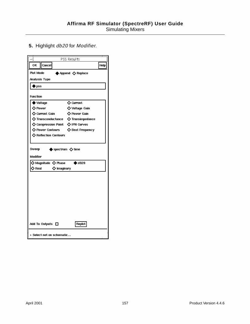
Affirma RF Simulator (SpectreRF) User GuideSimulating Mixers
5. Highlight db20 for Modifier.
April 2001 157 Product Version 4.4.6
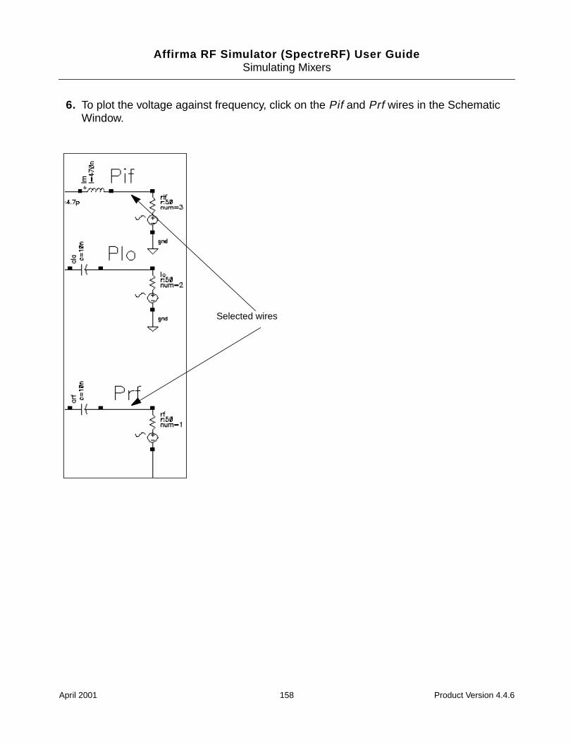
Affirma RF Simulator (SpectreRF) User GuideSimulating Mixers
6. To plot the voltage against frequency, click on the Pif and Prf wires in the SchematicWindow.
Selected wires
April 2001 158 Product Version 4.4.6
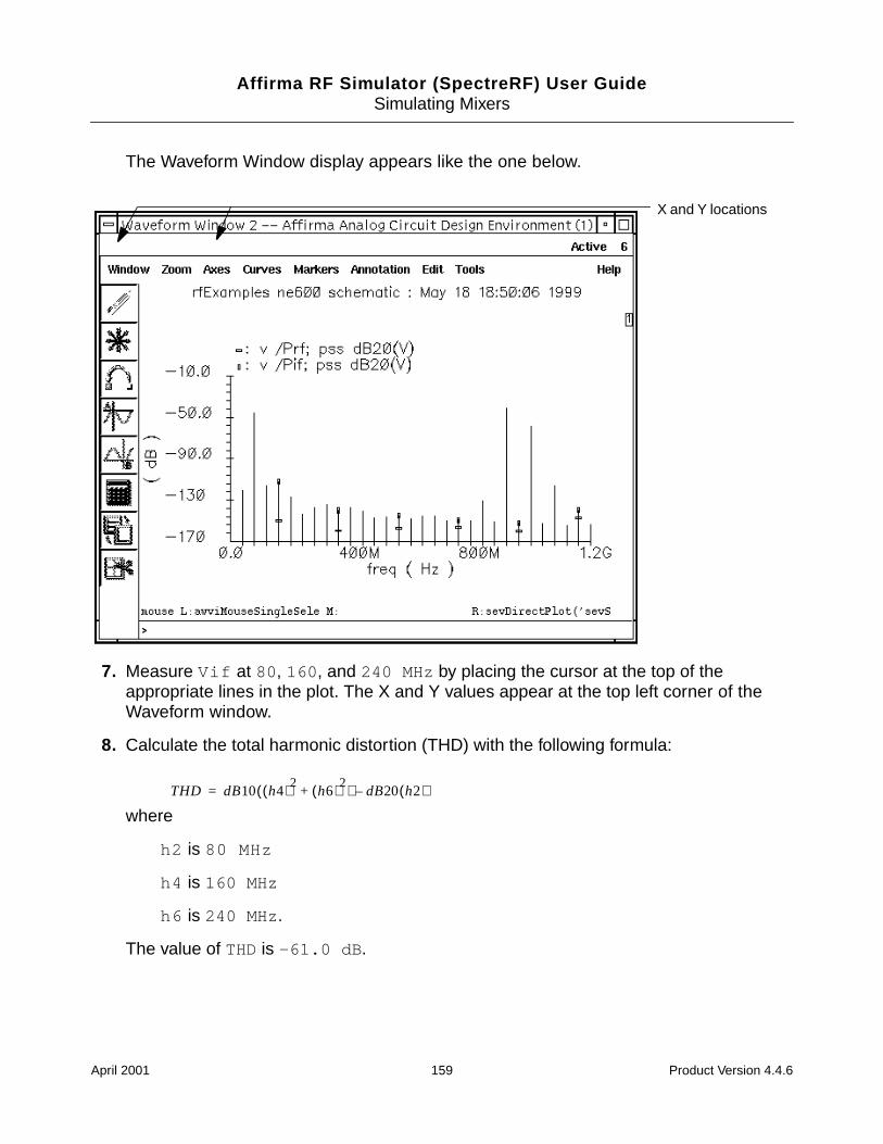
Affirma RF Simulator (SpectreRF) User GuideSimulating Mixers
The Waveform Window display appears like the one below.
7. Measure Vif at 80 , 160 , and 240 MHz by placing the cursor at the top of theappropriate lines in the plot. The X and Y values appear at the top left corner of theWaveform window.
8. Calculate the total harmonic distortion (THD) with the following formula:
where
h2 is 80 MHz
h4 is 160 MHz
h6 is 240 MHz .
The value of THD is -61.0 dB .
X and Y locations
THD dB10 h4( )2 h6( )2+( ) dB20 h2( )–=
April 2001 159 Product Version 4.4.6
Affirma RF Simulator (SpectreRF) User GuideSimulating Mixers
Noise Figure Measurement with PSS and Pnoise
You can combine a PSS analysis with a small-signal Pnoise analysis to determine the noisefigure for the ne600p circuit.
Pnoise analysis calculates the total noise at the output of the circuit. The equation for theNoise Figure is given in the SpectreRF Theory document. The SpectreRF Pnoise analysiscomputes the single sideband noise figure (-1 in this case). The total noise can vary with thenumber of harmonics you choose because each harmonic contributes a noise component.
Setting Up the Simulation
1. If necessary, open the ne600p mixer circuit.
2. If necessary, specify the full path to the model file in the Model File Set-up form.
3. In the Simulation window, use Analysis - Disable to disable any analyses you ranpreviously. (Check the Simulation window to verify whether or not an analysis isenabled.)
4. If necessary, set the design variables frf to 920Mand flo to 1G. (Check the Simulationwindow to verify the current design variable values.)
Editing The Schematic
Modify the schematic to be sure the PSS analysis is the response of the ne600p mixer to onlythe LO signal.
1. Choose Edit – Properties – Objects in the Schematic window.
The Edit Object Properties form appears. You use this form to change the list of CDFproperties and modify the schematic for this simulation.
2. In the Schematic Window, click on the rf voltage source.
April 2001 160 Product Version 4.4.6
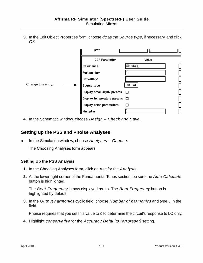
Affirma RF Simulator (SpectreRF) User GuideSimulating Mixers
3. In the Edit Object Properties form, choose dc as the Source type, if necessary, and clickOK.
4. In the Schematic window, choose Design – Check and Save.
Setting up the PSS and Pnoise Analyses
In the Simulation window, choose Analyses – Choose.
The Choosing Analyses form appears.
Setting Up the PSS Analysis
1. In the Choosing Analyses form, click on pss for the Analysis.
2. At the lower right corner of the Fundamental Tones section, be sure the Auto Calculatebutton is highlighted.
The Beat Frequency is now displayed as 1G. The Beat Frequency button ishighlighted by default.
3. In the Output harmonics cyclic field, choose Number of harmonics and type 0 in thefield.
Pnoise requires that you set this value to 0 to determine the circuit’s response to LO only.
4. Highlight conservative for the Accuracy Defaults (errpreset) setting.
Change this entry.
April 2001 161 Product Version 4.4.6
Affirma RF Simulator (SpectreRF) User GuideSimulating Mixers
Setting Up the Pnoise Analysis
1. At the top of the Choosing Analyses form, highlight pnoise.
The Choosing Analyses form changes to let you specify data for a Pnoise analysis.
2. In the Frequency Sweep Range (Hz) cyclic field, choose Start-Stop.
3. Type 1K and 2G as the Start and Stop values, respectively in the fields.
This frequency range covers the frequencies of interest, but avoids the value 0. Youcannot include the value 0 in a logarithmic sweep.
4. In the Sweep Type cyclic field, choose Logarithmic for the sweep type and highlight thePoints Per Decade button. Type 10 for the Points Per Decade value in the field.
5. In the Sidebands cyclic field, choose Maximum sideband and type 30 for the numberof sidebands.
With this setting, you specify that 30 sidebands contribute noise to the output. The valueis taken from the first example (PSS analysis only) in this chapter.
6. In the Output Voltage option cyclic field, choose voltage for the Output value.
7. Highlight the Positive Output Node Select button. Then click on the appropriate wirein the Schematic window to choose Pif.
/Pif appears in the Positive Output Node field.
8. Leave the Negative Output Node field empty.
This field defaults to /gnd! You can set the Negative Output Node to a different valueby clicking on the Negative Output Node Select button and then choosing the outputnode in the schematic.
9. In the Input Source cyclic field, choose voltage.
10. Click on the Input Voltage Source Select button. Then click on the appropriatecomponent in the Schematic window to choose rf.
/rf appears in the Input Voltage Source field.
11. Type -1 in the Reference Sideband field.
In this field, you specify the difference between the input and output frequencies in thewhole frf. The Reference Sideband must be -1 because this is a down converter.Other possible choices are 0 and +1.
April 2001 162 Product Version 4.4.6
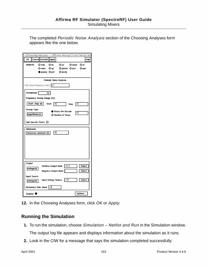
Affirma RF Simulator (SpectreRF) User GuideSimulating Mixers
The completed Periodic Noise Analysis section of the Choosing Analyses formappears like the one below.
12. In the Choosing Analyses form, click OK or Apply.
Running the Simulation
1. To run the simulation, choose Simulation – Netlist and Run in the Simulation window.
The output log file appears and displays information about the simulation as it runs.
2. Look in the CIW for a message that says the simulation completed successfully.
April 2001 163 Product Version 4.4.6
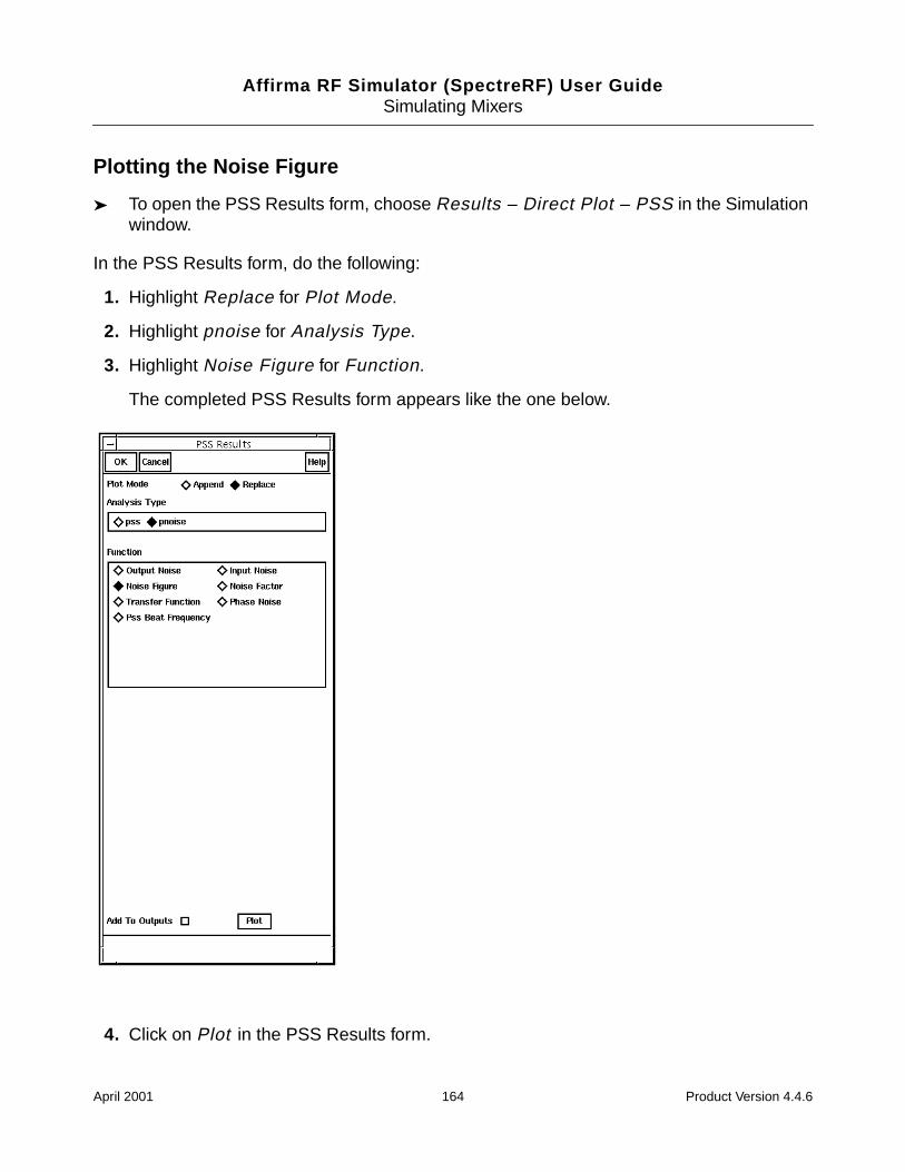
Affirma RF Simulator (SpectreRF) User GuideSimulating Mixers
Plotting the Noise Figure
To open the PSS Results form, choose Results – Direct Plot – PSS in the Simulationwindow.
In the PSS Results form, do the following:
1. Highlight Replace for Plot Mode.
2. Highlight pnoise for Analysis Type.
3. Highlight Noise Figure for Function.
The completed PSS Results form appears like the one below.
4. Click on Plot in the PSS Results form.
April 2001 164 Product Version 4.4.6
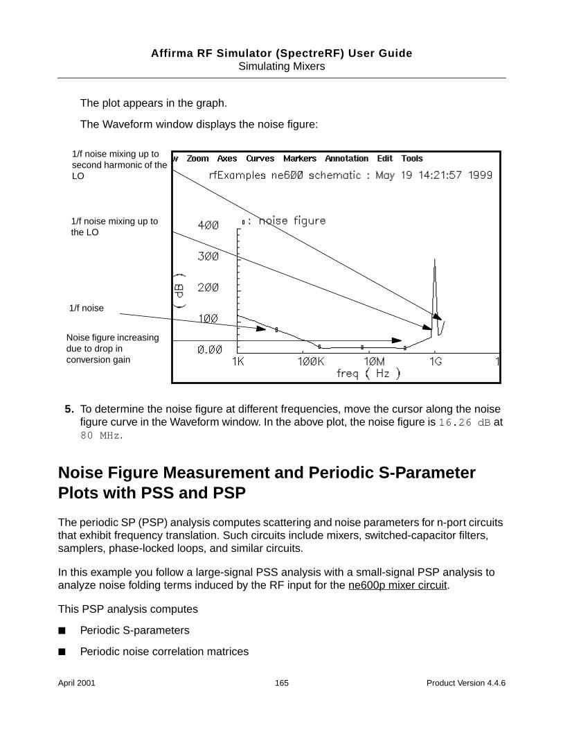
Affirma RF Simulator (SpectreRF) User GuideSimulating Mixers
The plot appears in the graph.
The Waveform window displays the noise figure:
5. To determine the noise figure at different frequencies, move the cursor along the noisefigure curve in the Waveform window. In the above plot, the noise figure is 16.26 dB at80 MHz .
Noise Figure Measurement and Periodic S-ParameterPlots with PSS and PSP
The periodic SP (PSP) analysis computes scattering and noise parameters for n-port circuitsthat exhibit frequency translation. Such circuits include mixers, switched-capacitor filters,samplers, phase-locked loops, and similar circuits.
In this example you follow a large-signal PSS analysis with a small-signal PSP analysis toanalyze noise folding terms induced by the RF input for the ne600p mixer circuit.
This PSP analysis computes
Periodic S-parameters
Periodic noise correlation matrices
Noise figure increasingdue to drop inconversion gain
1/f noise
1/f noise mixing up tothe LO
1/f noise mixing up tosecond harmonic of theLO
April 2001 165 Product Version 4.4.6
Affirma RF Simulator (SpectreRF) User GuideSimulating Mixers
Noise figure
Equivalent noise parameters
The PSP analysis is a small-signal analysis like the SP analysis, except that, as is true forPAC and PXF analysis, the circuit is first linearized about a periodically varying operatingpoint as opposed to a simple DC operating point. Linearizing the circuit about a periodicallytime-varying operating point allows for the computation of S-parameters between circuit portsthat convert signals from one frequency band to another.
The PSP analysis can also calculate noise parameters in frequency-converting circuits. PSPcomputes noise figure (both single-sideband and double-sideband), input referred noise,equivalent noise parameters, and noise correlation matrices. The noise features of the PSPanalysis include noise folding effects due to the periodically time-varying nature of the circuit.This is also true for the Pnoise analysis, but not for the SP analysis.
Setting Up the Simulation
1. If necessary, open the ne600p mixer circuit.
2. If necessary, specify the full path to the model file in the Model File Set-up form.
3. In the Simulation window, use Analysis - Disable to disable any analyses you ranpreviously. (Check the Simulation window to verify whether or not an analysis isenabled.)
4. If necessary, set the design variables frf to 900Mand flo to 1G. (Check the Simulationwindow to verify the current design variable values.)
Editing the Schematic
The rf source used in the ne600p mixer circuit has a Source type property that you can setto either sine or dc depending on your application. Suppose that your RF input signal is at900 MHz, the LO is at 1 GHz, and the IF is at 100 MHz. Before you perform a PSP analysis,you must first perform a PSS analysis.
In many cases for small-signal analysis, it is sufficient to treat the RF input as a small-signal. For example, most gain measurements are performed under small-signalconditions in which case you set the Source type to dc.
When it is important to analyze additional noise folding terms induced by the rf input, youtreat the rf source as a large signal in which case you set the Source type to sine.
See Appendix L, “Using PSP and Pnoise Analyses” for more information.
April 2001 166 Product Version 4.4.6
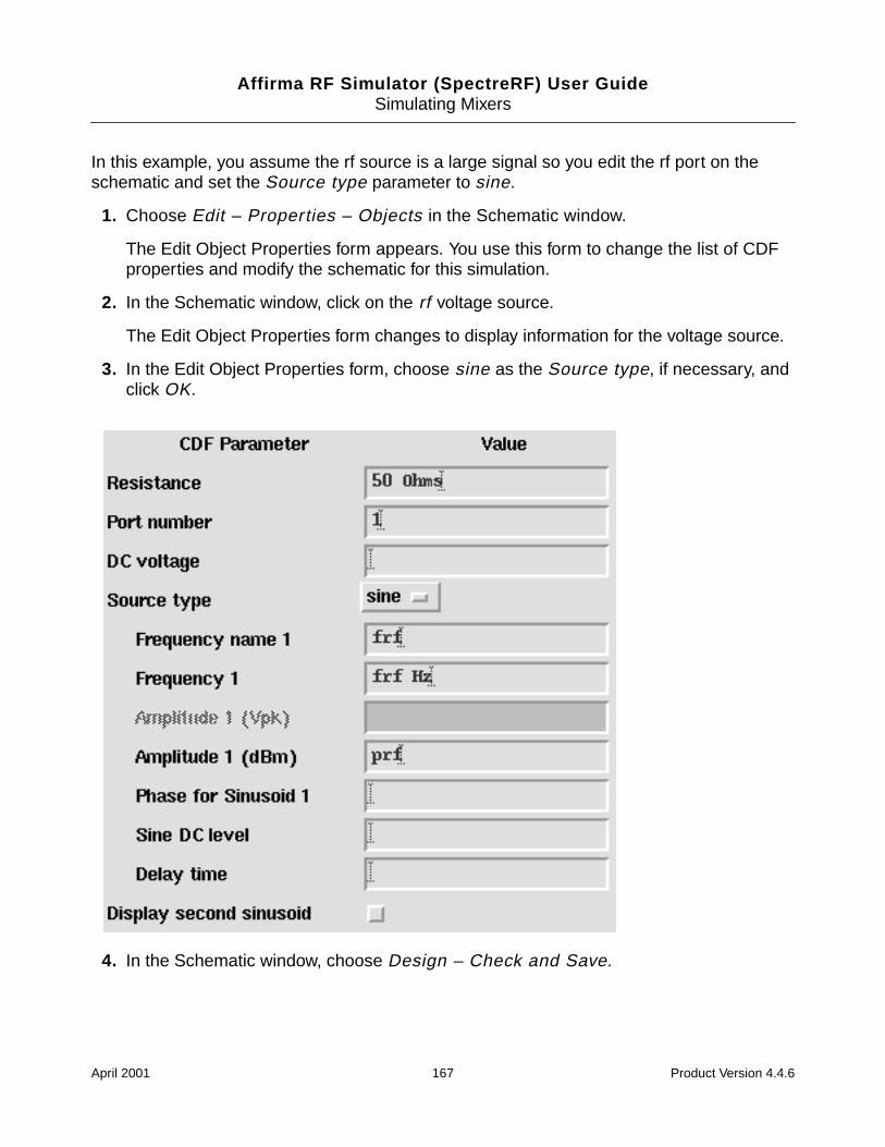
Affirma RF Simulator (SpectreRF) User GuideSimulating Mixers
In this example, you assume the rf source is a large signal so you edit the rf port on theschematic and set the Source type parameter to sine.
1. Choose Edit – Properties – Objects in the Schematic window.
The Edit Object Properties form appears. You use this form to change the list of CDFproperties and modify the schematic for this simulation.
2. In the Schematic window, click on the rf voltage source.
The Edit Object Properties form changes to display information for the voltage source.
3. In the Edit Object Properties form, choose sine as the Source type, if necessary, andclick OK.
4. In the Schematic window, choose Design – Check and Save.
April 2001 167 Product Version 4.4.6
Affirma RF Simulator (SpectreRF) User GuideSimulating Mixers
Setting up the PSS and PSP Analyses
Use the Choosing Analyses form, to set up two analyses, first PSS then PSP.
Choose Analyses – Choose in the Simulation window.
The Choosing Analyses form appears.
Setting Up the PSS Analysis
1. At the top of the Choosing Analyses form, highlight pss.
2. In the Fundamental Tones list box, be sure the Auto Calculate button is highlighted.
The Beat Frequency is now displayed. (The Beat Frequency button is highlighted bydefault.) The 100 M value for beat frequency is the minimum period for which both RF at900 MHz and LO at 1 GHz are periodic (or for which RF and LO are integer multiples ofthe fundamental frequency).
3. In the Output harmonics cyclic field, choose Number of harmonics. Type 30 in theNumber of harmonics field.
This entry expands the plotted frequency range to include the areas of interest aroundboth 100 MHz and 1 GHz. (30 × 100 MHz equals 3GHz, or 0 to 3GHz, and includes allimportant frequencies.)
4. Highlight moderate for the Accuracy Defaults (errpreset) setting.
5. Be sure the Enabled button is highlighted.
April 2001 168 Product Version 4.4.6
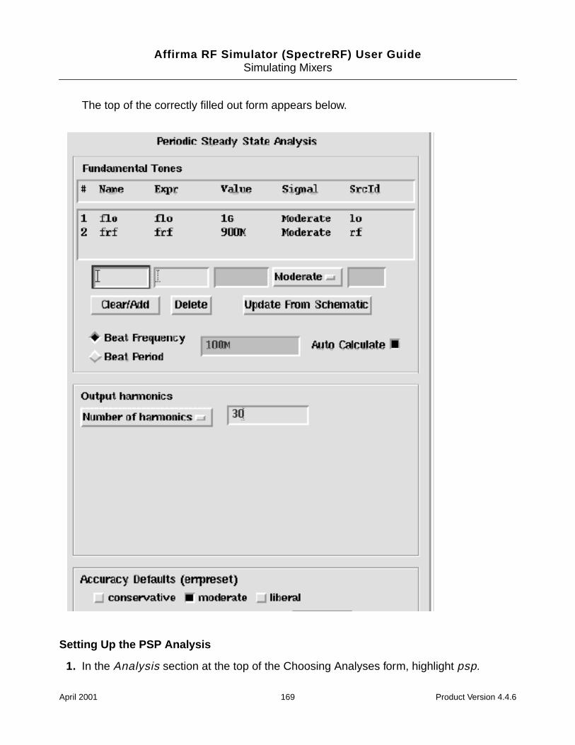
Affirma RF Simulator (SpectreRF) User GuideSimulating Mixers
The top of the correctly filled out form appears below.
Setting Up the PSP Analysis
1. In the Analysis section at the top of the Choosing Analyses form, highlight psp.
April 2001 169 Product Version 4.4.6
Affirma RF Simulator (SpectreRF) User GuideSimulating Mixers
The Choosing Analyses form changes to let you specify data for the PSP analysis.
2. In the Sweeptype cyclic field, choose relative.
The Sweeptype parameter controls the way that frequencies are swept in the PSPanalysis. When you specify a relative sweep, the sweep is relative to the analysisharmonics (not the PSS fundamental frequency).
For PSP analysis, the frequencies of the input and response are usually different. This isan important difference between the PSP and SP analyses. Because the PSPcomputation involves inputs and outputs at frequencies that are relative to multipleharmonics, the freqaxis and sweeptype parameters behave somewhat differently inPSP analysis than they behave in PAC and PXF analyses.
3. In the Frequency Sweep Range (Hz) cyclic field, choose Start-Stop and type -20Mand 30M, respectively, in the Start and Stop fields.
The PSP analysis is performed from 20 MHz below the RF center frequency to 30 MHzabove it. This frequency range accounts for inputs on the rf port in the range of -920 MHzto -870 MHz. Noise parameters (such as noise figure) are computed in a 50 MHz bandaround the frequency specified by the output harmonic.
4. Leave the Sweep Type cyclic field set to Automatic.
5. Highlight Select Ports to select the input and output ports on the schematic.
The input port is the rf port and the output port is the rif port.
6. Click the Input Port (#1) Select button. Then, in the Schematic window, click on theappropriate port to choose /rf .
/rf appears in the Input Port (#1) field.
7. Click the Output Port (#2) Select button. Then, in the Schematic window, click on theappropriate port to choose /rif .
/rif appears in the Output Port (#2) field.
8. Leave the Aux Port (#3) field empty.
This field is used to include in the analysis an additional port/harmonic pair.
9. Type -9 in the Input Port (#1) Harmonic field. Type 1 in the Output Port (#2)Harmonic field.
With the 1 GHz LO, small-signal inputs around 900 MHz (harmonics +/-9 of the PSSfundamental) appear at around 100 MHz (or harmonics -/+1 of the fundamental). Youselect harmonic 1 as the output harmonic, and harmonic -9 as the input harmonic
April 2001 170 Product Version 4.4.6
Affirma RF Simulator (SpectreRF) User GuideSimulating Mixers
because a single complex-exponential input ( ) on the lower side of 900 MHz(harmonic -9) appears as the upper sideband of harmonic 1 at around 100 MHz.
Harmonics -9 and 1 are separated by 10 fundamental periods, which corresponds to theLO frequency of 1 GHz.
10. Below Do Noise near the bottom of the form, highlight Yes to calculate noise parametersas part of the PSP analysis.
11. Type 50 in the Maxsideband field.
Setting Maxsideband to 50 accounts for noise folding from up to 5 GHz in frequency.
All noise computations in PSP analysis involve noise folding effects. The maxsidebandparameter specifies the maximum sideband to include for summing noise contributionseither up-converted or down-converted to the output at the frequency of interest.
12. Click the Options button to display the PSP Options form.
eiωst
April 2001 171 Product Version 4.4.6
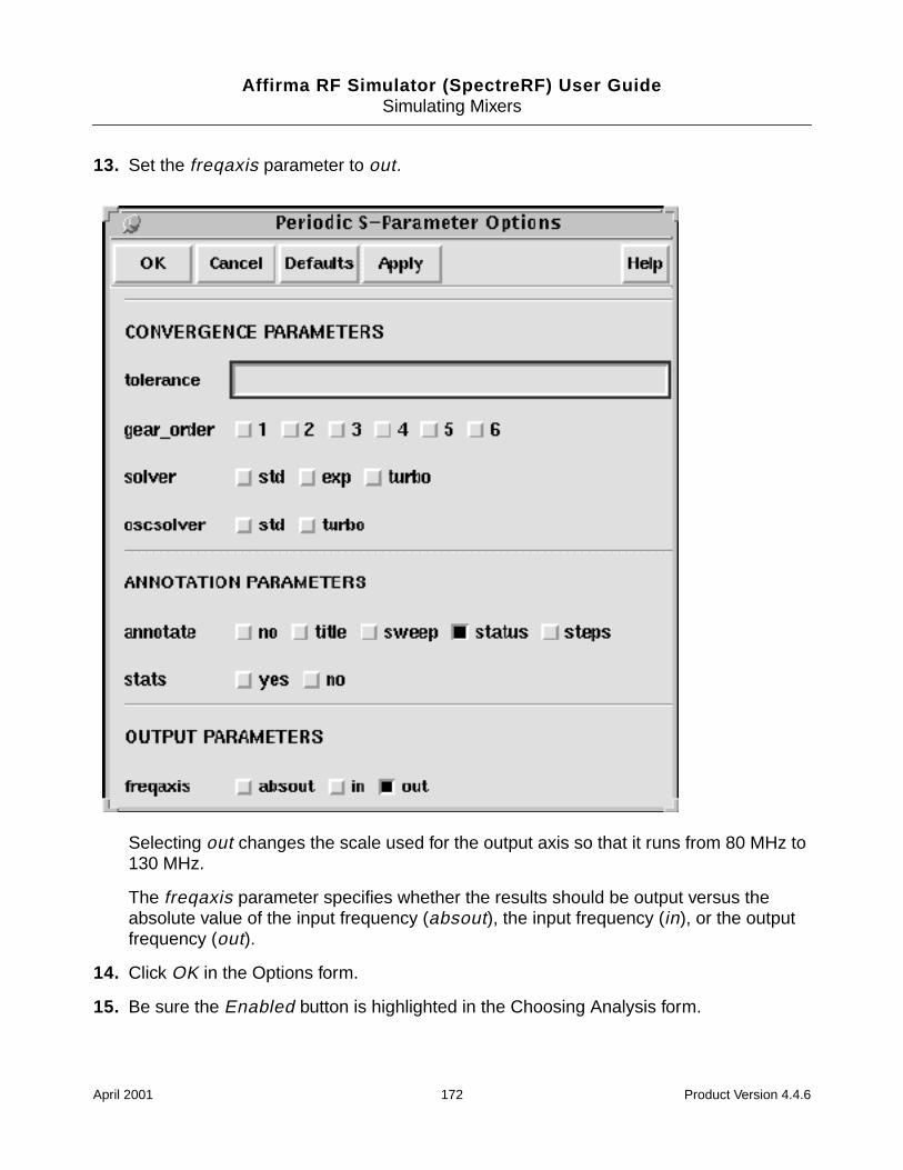
Affirma RF Simulator (SpectreRF) User GuideSimulating Mixers
13. Set the freqaxis parameter to out.
Selecting out changes the scale used for the output axis so that it runs from 80 MHz to130 MHz.
The freqaxis parameter specifies whether the results should be output versus theabsolute value of the input frequency (absout), the input frequency (in), or the outputfrequency (out).
14. Click OK in the Options form.
15. Be sure the Enabled button is highlighted in the Choosing Analysis form.
April 2001 172 Product Version 4.4.6
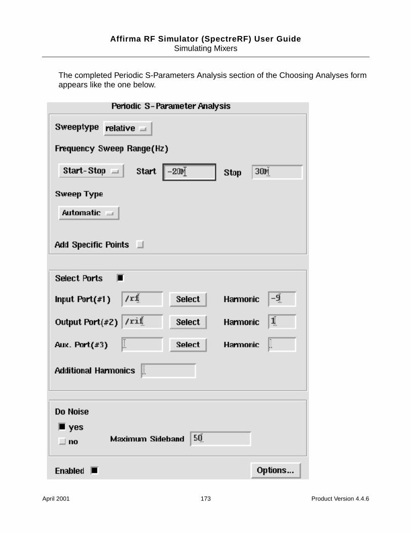
Affirma RF Simulator (SpectreRF) User GuideSimulating Mixers
The completed Periodic S-Parameters Analysis section of the Choosing Analyses formappears like the one below.
April 2001 173 Product Version 4.4.6
Affirma RF Simulator (SpectreRF) User GuideSimulating Mixers
16. In the Choosing Analyses form, click OK.
Running the Simulation
You can now run the simulation. In addition to computing the periodic S-parameters, theperiodic noise correlation matrixes are also computed, as are noise figure and the equivalentnoise parameters.
1. To run the simulation, choose Simulation – Netlist and Run in the Simulation window.
The output log file appears and displays information about the simulation as it runs.
2. Look in the CIW for a message that says the simulation completed successfully.
Plotting the Noise Figure
To open the PSS Results form, choose Results – Direct Plot – PSS in the Simulationwindow.
In the PSS Results form, do the following:
1. Highlight Replace for Plot Mode.
2. Highlight psp for Analysis.
3. Highlight NF for Function to display the Noise Figure.
April 2001 174 Product Version 4.4.6
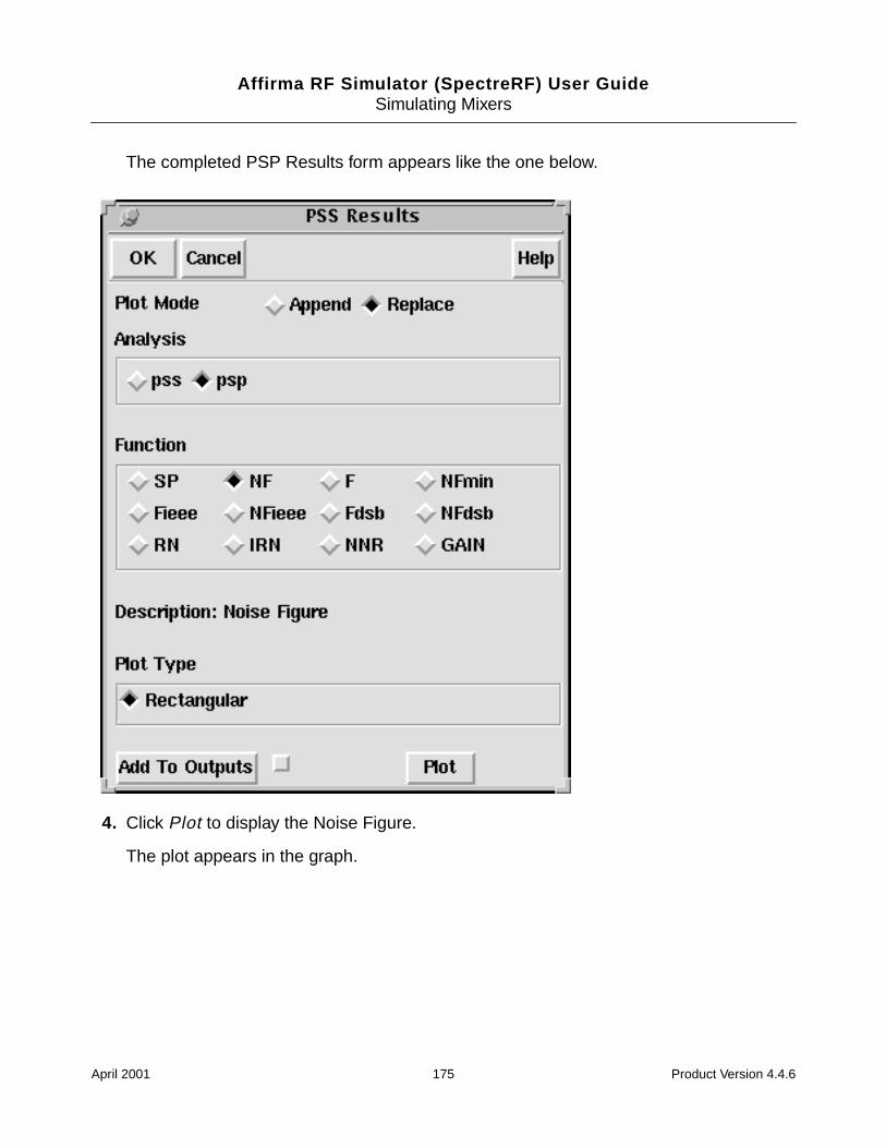
Affirma RF Simulator (SpectreRF) User GuideSimulating Mixers
The completed PSP Results form appears like the one below.
4. Click Plot to display the Noise Figure.
The plot appears in the graph.
April 2001 175 Product Version 4.4.6
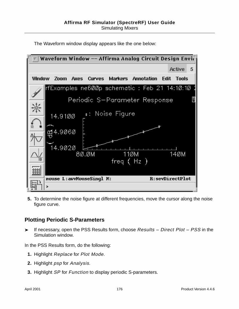
Affirma RF Simulator (SpectreRF) User GuideSimulating Mixers
The Waveform window display appears like the one below:
5. To determine the noise figure at different frequencies, move the cursor along the noisefigure curve.
Plotting Periodic S-Parameters
If necessary, open the PSS Results form, choose Results – Direct Plot – PSS in theSimulation window.
In the PSS Results form, do the following:
1. Highlight Replace for Plot Mode.
2. Highlight psp for Analysis.
3. Highlight SP for Function to display periodic S-parameters.
April 2001 176 Product Version 4.4.6

Affirma RF Simulator (SpectreRF) User GuideSimulating Mixers
4. Highlight Z-Smith for Plot Type to display periodic S-parameters.
5. Click S22 to plot output match
Recall from basic S-parameter theory that for a 2-port circuit S22 represents the matchat port 2. In this example S22 represents the match at the if port.
April 2001 177 Product Version 4.4.6
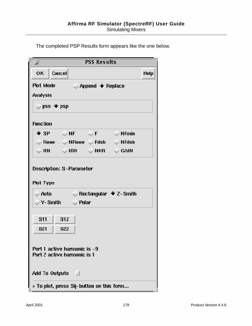
Affirma RF Simulator (SpectreRF) User GuideSimulating Mixers
The completed PSP Results form appears like the one below.
April 2001 178 Product Version 4.4.6
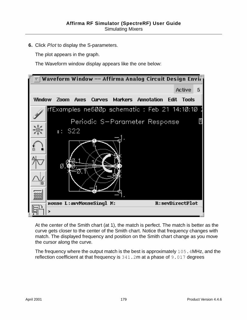
Affirma RF Simulator (SpectreRF) User GuideSimulating Mixers
6. Click Plot to display the S-parameters.
The plot appears in the graph.
The Waveform window display appears like the one below:
At the center of the Smith chart (at 1), the match is perfect. The match is better as thecurve gets closer to the center of the Smith chart. Notice that frequency changes withmatch. The displayed frequency and position on the Smith chart change as you movethe cursor along the curve.
The frequency where the output match is the best is approximately 105.4 MHz, and thereflection coefficient at that frequency is 341.2 m at a phase of 9.017 degrees
April 2001 179 Product Version 4.4.6
Affirma RF Simulator (SpectreRF) User GuideSimulating Mixers
Conversion Gain Measurement with PSS and PXF
You can combine a PSS analysis with a periodic small-signal transfer function PXF analysisto determine the conversion gain of the down converter. With changes to the plotting form,you can also calculate the power supply rejection and local oscillator feedthrough.
Setting Up the Simulation
1. If necessary, open the ne600p mixer circuit.
2. If necessary, specify the full path to the model file in the Model File Set-up form.
3. In the Simulation window, use Analysis - Disable to disable any analyses you ranpreviously. (Check the Simulation window to verify whether or not an analysis isenabled.)
4. If necessary, set the design variables frf to 920Mand flo to 1G. (Check the Simulationwindow to verify the current design variable values.)
Editing the Schematic
You must modify the schematic to set the RF source to a DC source to be sure the PSSanalysis is the response of the ne600p mixer to only the LO signal.
1. Choose Edit – Properties – Objects in the Schematic window.
The Edit Object Properties form appears. You use this form to change the list of CDFproperties and modify the schematic for this simulation.
2. In the Schematic window, click on the rf voltage source.
April 2001 180 Product Version 4.4.6
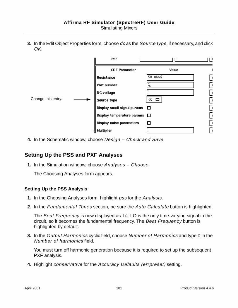
Affirma RF Simulator (SpectreRF) User GuideSimulating Mixers
3. In the Edit Object Properties form, choose dc as the Source type, if necessary, and clickOK.
4. In the Schematic window, choose Design – Check and Save.
Setting Up the PSS and PXF Analyses
1. In the Simulation window, choose Analyses – Choose.
The Choosing Analyses form appears.
Setting Up the PSS Analysis
1. In the Choosing Analyses form, highlight pss for the Analysis.
2. In the Fundamental Tones section, be sure the Auto Calculate button is highlighted.
The Beat Frequency is now displayed as 1G. LO is the only time-varying signal in thecircuit, so it becomes the fundamental frequency. The Beat Frequency button ishighlighted by default.
3. In the Output Harmonics cyclic field, choose Number of Harmonics and type 0 in theNumber of harmonics field.
You must turn off harmonic generation because it is required to set up the subsequentPXF analysis.
4. Highlight conservative for the Accuracy Defaults (errpreset) setting.
Change this entry.
April 2001 181 Product Version 4.4.6
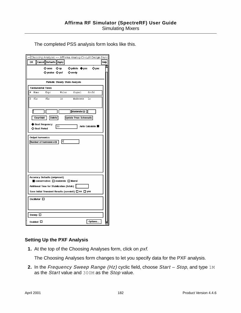
Affirma RF Simulator (SpectreRF) User GuideSimulating Mixers
The completed PSS analysis form looks like this.
Setting Up the PXF Analysis
1. At the top of the Choosing Analyses form, click on pxf.
The Choosing Analyses form changes to let you specify data for the PXF analysis.
2. In the Frequency Sweep Range (Hz) cyclic field, choose Start – Stop, and type 1Mas the Start value and 300M as the Stop value.
April 2001 182 Product Version 4.4.6

Affirma RF Simulator (SpectreRF) User GuideSimulating Mixers
This range specification leaves space between the plots, but still shows the dramatic gainchanges in the first 100 Mhz of each plot.
3. In the Sweep Type cyclic field, choose Linear and highlight Number of Steps. Type50 for the Number of Steps.
Larger numbers of total points increase the resolution of the plot but also require a longersimulation time.
4. In the Sidebands cyclic field, choose Maximum sideband and type 3 as the value.
5. In the Output section, highlight voltage.
6. Click on the Positive Output Node Select button. Then click on the appropriate wire inthe Schematic window to choose Pif.
/Pif appears in the Positive Output Node field.
7. Leave the Negative Output Node field empty.
This field defaults to /gnd! You can set the Negative Output Node to a different valueby clicking on the Negative Output Node Select button and then choosing the outputnode in the schematic.
April 2001 183 Product Version 4.4.6
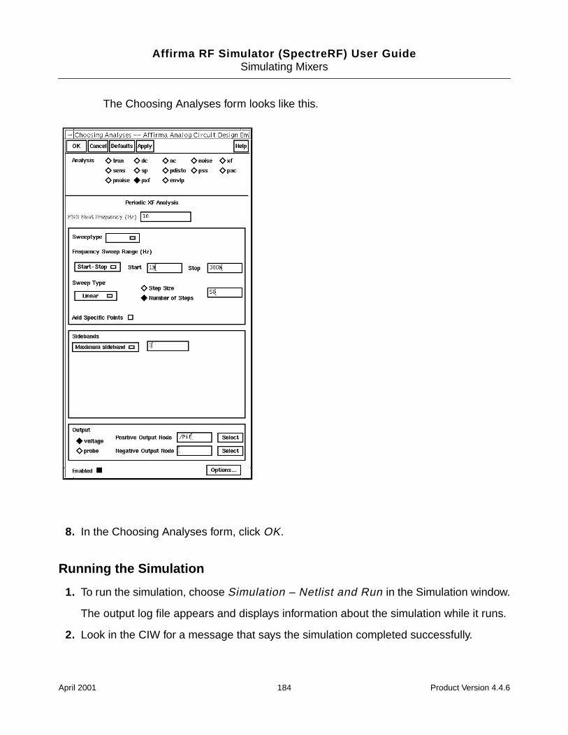
Affirma RF Simulator (SpectreRF) User GuideSimulating Mixers
The Choosing Analyses form looks like this.
8. In the Choosing Analyses form, click OK.
Running the Simulation
1. To run the simulation, choose Simulation – Netlist and Run in the Simulation window.
The output log file appears and displays information about the simulation while it runs.
2. Look in the CIW for a message that says the simulation completed successfully.
April 2001 184 Product Version 4.4.6

Affirma RF Simulator (SpectreRF) User GuideSimulating Mixers
Plotting the Conversion Gain
Choose Results – Direct Plot – PSS in the Simulation window.
The PSS Results form appears.
In the PSS Results form, do the following:
1. Highlight Replace for Plot Mode.
2. Highlight pxf for Analysis Type.
3. Highlight Voltage Gain for Function.
4. Highlight sideband for Sweep.
5. Highlight dB20 for Modifier.
6. Highlight -1 and 1 for Output Sideband.
You must hold the Control key down while you highlight the second sideband.
April 2001 185 Product Version 4.4.6
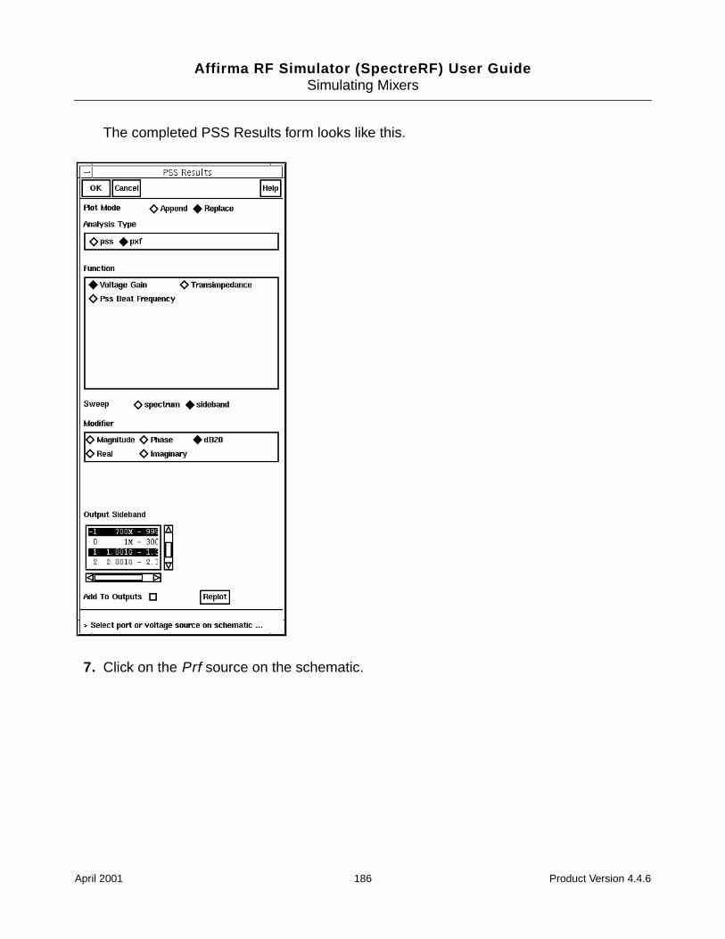
Affirma RF Simulator (SpectreRF) User GuideSimulating Mixers
The completed PSS Results form looks like this.
7. Click on the Prf source on the schematic.
April 2001 186 Product Version 4.4.6
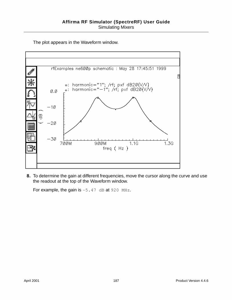
Affirma RF Simulator (SpectreRF) User GuideSimulating Mixers
The plot appears in the Waveform window.
8. To determine the gain at different frequencies, move the cursor along the curve and usethe readout at the top of the Waveform window.
For example, the gain is -5.47 dB at 920 MHz .
April 2001 187 Product Version 4.4.6
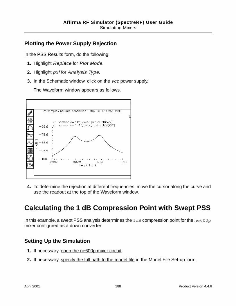
Affirma RF Simulator (SpectreRF) User GuideSimulating Mixers
Plotting the Power Supply Rejection
In the PSS Results form, do the following:
1. Highlight Replace for Plot Mode.
2. Highlight pxf for Analysis Type.
3. In the Schematic window, click on the vcc power supply.
The Waveform window appears as follows.
4. To determine the rejection at different frequencies, move the cursor along the curve anduse the readout at the top of the Waveform window.
Calculating the 1 dB Compression Point with Swept PSS
In this example, a swept PSS analysis determines the 1dB compression point for the ne600pmixer configured as a down converter.
Setting Up the Simulation
1. If necessary, open the ne600p mixer circuit.
2. If necessary, specify the full path to the model file in the Model File Set-up form.
April 2001 188 Product Version 4.4.6
Affirma RF Simulator (SpectreRF) User GuideSimulating Mixers
3. In the Simulation window, use Analysis - Disable to disable any analyses you ranpreviously. (Check the Simulation window to verify whether or not an analysis isenabled.)
4. If necessary, set the design variables frf to 920Mand flo to 1G. (Check the Simulationwindow to verify the current design variable values.)
Editing the Schematic
1. In the Schematic window, click on the rf voltage source.
2. Choose Edit – Properties – Objects in the Schematic window.
The Edit Object Properties form appears. You use this form to change the list of CDFproperties and modify the schematic for this simulation.
3. In the Edit Object Properties form, specify the following and click OK.
Choose sine for Source type, and type prf in the Amplitude (dBm) field.
4. In the Schematic window, choose Design – Check and Save.
Setting Up the Swept PSS Analysis
1. In the Simulation window, choose Analyses – Choose.
The Choosing Analyses form appears.
2. In the Choosing Analyses form, choose pss for the Analysis.
3. In the Fundamental Tones list box, be sure the Auto Calculate button is highlighted.
The Beat Frequency is now displayed as 40M. Now that the RF signal is active again,the fundamental frequency of the circuit goes back to 40 MHz . The Beat Frequencybutton is highlighted by default.
4. In the Output harmonics cyclic field, choose Number of harmonics and type 2 in theNumber of harmonics field.
Only two harmonics are required to determine the 1 dB compression point.
5. Highlight conservative for the Accuracy Defaults (errpreset) setting.
6. Highlight the Sweep button.
The form changes to let you specify data for the sweep.
7. In the Sweep cyclic field, choose Variable.
April 2001 189 Product Version 4.4.6
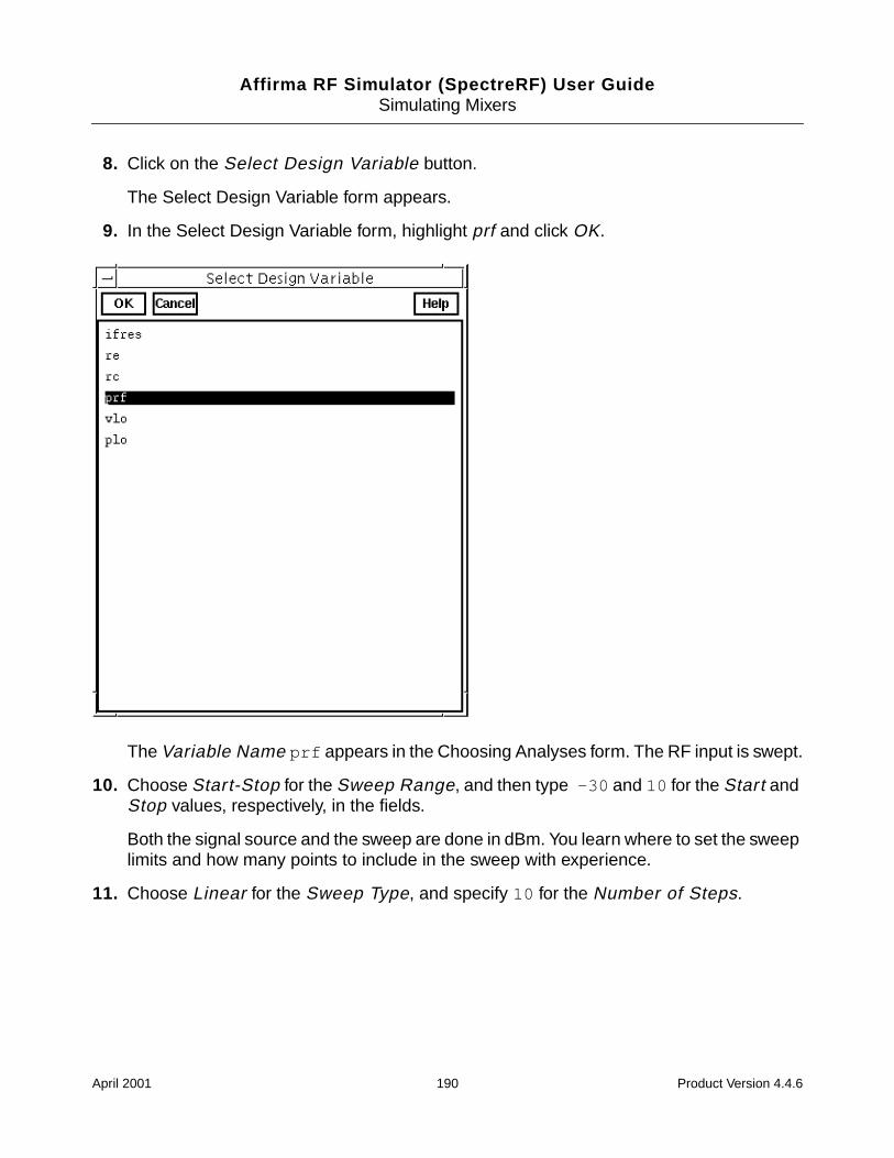
Affirma RF Simulator (SpectreRF) User GuideSimulating Mixers
8. Click on the Select Design Variable button.
The Select Design Variable form appears.
9. In the Select Design Variable form, highlight prf and click OK.
The Variable Name prf appears in the Choosing Analyses form. The RF input is swept.
10. Choose Start-Stop for the Sweep Range, and then type -30 and 10 for the Start andStop values, respectively, in the fields.
Both the signal source and the sweep are done in dBm. You learn where to set the sweeplimits and how many points to include in the sweep with experience.
11. Choose Linear for the Sweep Type, and specify 10 for the Number of Steps.
April 2001 190 Product Version 4.4.6
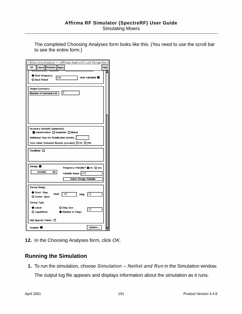
Affirma RF Simulator (SpectreRF) User GuideSimulating Mixers
The completed Choosing Analyses form looks like this. (You need to use the scroll barto see the entire form.)
12. In the Choosing Analyses form, click OK.
Running the Simulation
1. To run the simulation, choose Simulation – Netlist and Run in the Simulation window.
The output log file appears and displays information about the simulation as it runs.
April 2001 191 Product Version 4.4.6
Affirma RF Simulator (SpectreRF) User GuideSimulating Mixers
2. Look in the CIW for a message that says the simulation completed successfully.
Plotting the 1 dB Compression Point
The first sideband of the IF signal is the second harmonic of the 40 MHz fundamental. To plotthe 1 dB compression point, perform the following:
Choose Results – Direct Plot – PSS in the Simulation window.
The PSS Results form appears.
In the PSS Results form, do the following:
1. Highlight Replace for Plot Mode.
2. Highlight pss for Analysis Type.
3. Highlight Compression Point for Function.
4. Type 1 for Gain Compression (dB).
5. Type -25 for Extrapolation Point (dBm).
This value specifies the point where the ideal amplification curve intersects the outputcurve. You must estimate where this point is located. If you do not specify a value, theplot defaults to the minimum variable value.
6. Choose Input Referred 1dB Compression.
7. In the Harmonic list box, highlight harmonic 2 (80 MHz).
This is the second harmonic of the 40 MHz fundamental frequency, which is the IFfrequency.
April 2001 192 Product Version 4.4.6
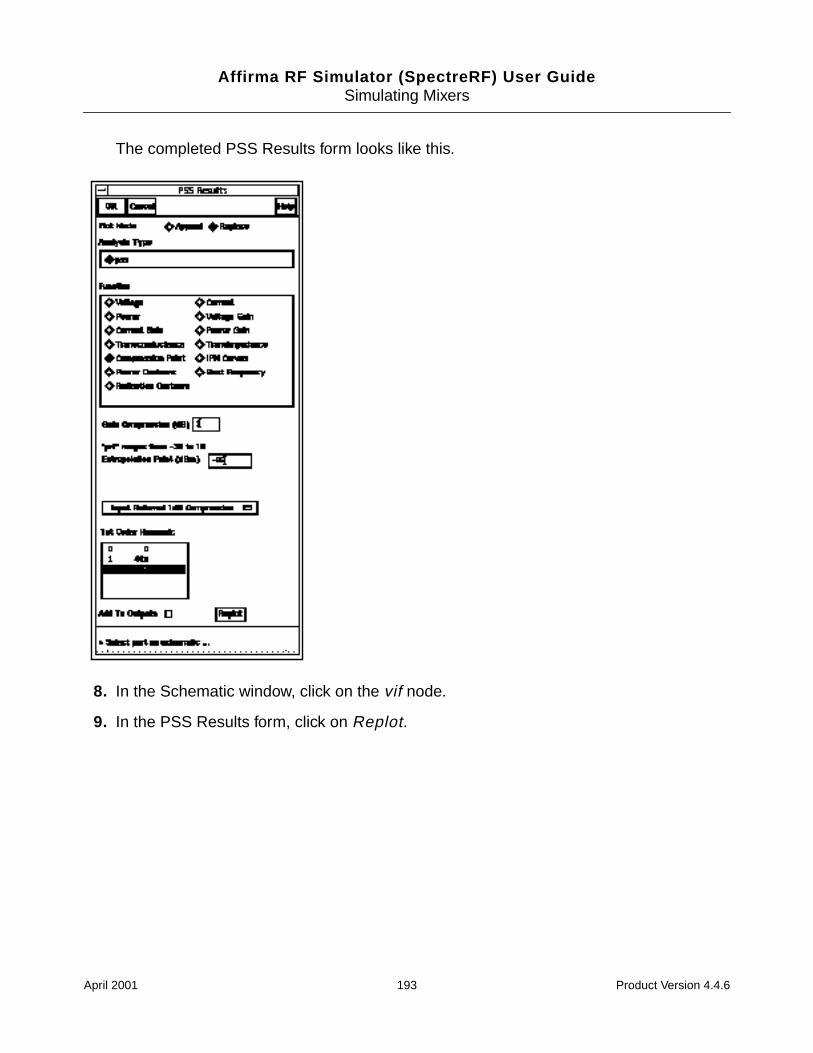
Affirma RF Simulator (SpectreRF) User GuideSimulating Mixers
The completed PSS Results form looks like this.
8. In the Schematic window, click on the vif node.
9. In the PSS Results form, click on Replot.
April 2001 193 Product Version 4.4.6
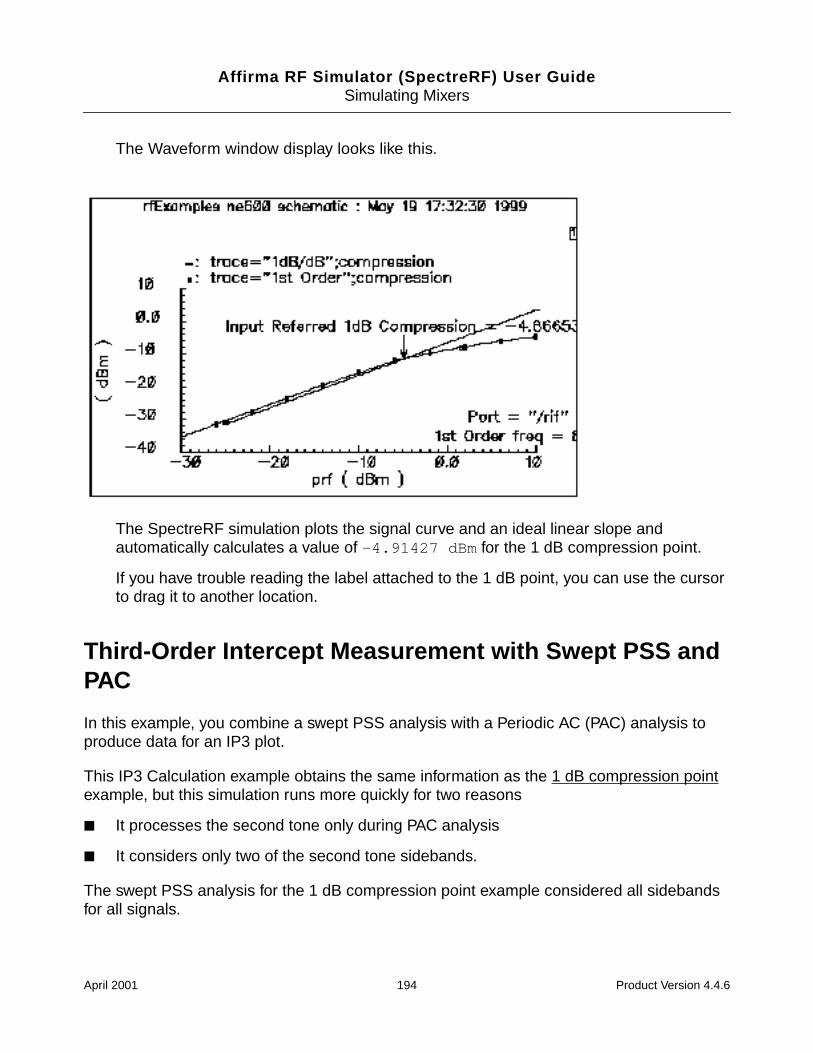
Affirma RF Simulator (SpectreRF) User GuideSimulating Mixers
The Waveform window display looks like this.
The SpectreRF simulation plots the signal curve and an ideal linear slope andautomatically calculates a value of -4.91427 dBm for the 1 dB compression point.
If you have trouble reading the label attached to the 1 dB point, you can use the cursorto drag it to another location.
Third-Order Intercept Measurement with Swept PSS andPAC
In this example, you combine a swept PSS analysis with a Periodic AC (PAC) analysis toproduce data for an IP3 plot.
This IP3 Calculation example obtains the same information as the 1 dB compression pointexample, but this simulation runs more quickly for two reasons
It processes the second tone only during PAC analysis
It considers only two of the second tone sidebands.
The swept PSS analysis for the 1 dB compression point example considered all sidebandsfor all signals.
April 2001 194 Product Version 4.4.6
Affirma RF Simulator (SpectreRF) User GuideSimulating Mixers
Setting Up the Simulation
1. If necessary, open the ne600p mixer circuit.
2. If necessary, specify the full path to the model file in the Model File Set-up form.
3. In the Simulation window, use Analysis - Disable to disable any analyses you ranpreviously. (Check the Simulation window to verify whether or not an analysis isenabled.)
4. If necessary, set the design variables frf to 920Mand flo to 1G. (Check the Simulationwindow to verify the current design variable values.)
Editing the Schematic
1. In the Schematic window, choose Edit – Properties – Objects.
The Edit Object Properties form appears. You use this form to modify the schematic bychanging the list of CDF properties.
2. To modify the schematic for this simulation, click on the rf voltage source in theSchematic window.
In the Edit Object Properties form, do the following:
1. Highlight Display second sinusoid and remove any values that are set from previousanalyses.
2. Choose sine for Source type.
3. Type frf for Frequency.
4. Type prf in the Amplitude (dBm) field.
5. Highlight Display small signal params.
The form changes to let you specify small signal parameters.
6. Type prf for the PAC Magnitude (dBm) value.
April 2001 195 Product Version 4.4.6
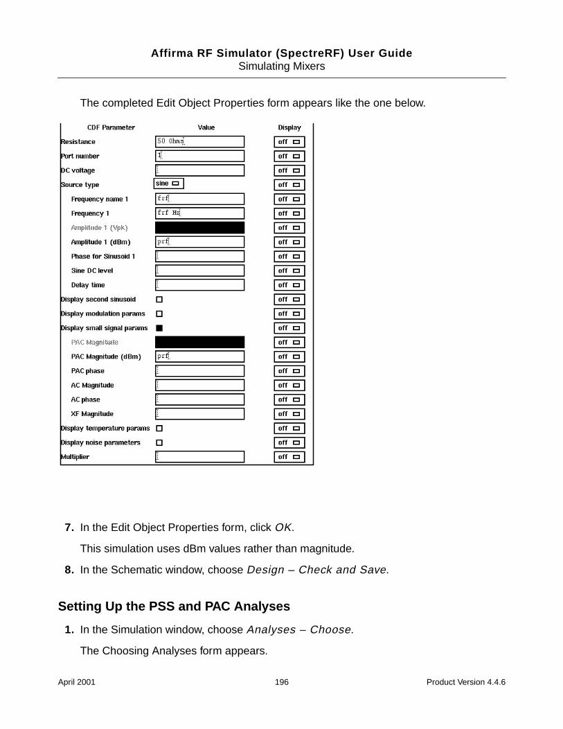
Affirma RF Simulator (SpectreRF) User GuideSimulating Mixers
The completed Edit Object Properties form appears like the one below.
7. In the Edit Object Properties form, click OK.
This simulation uses dBm values rather than magnitude.
8. In the Schematic window, choose Design – Check and Save.
Setting Up the PSS and PAC Analyses
1. In the Simulation window, choose Analyses – Choose.
The Choosing Analyses form appears.
April 2001 196 Product Version 4.4.6
Affirma RF Simulator (SpectreRF) User GuideSimulating Mixers
Setting Up the PSS Analysis
1. In the Choosing Analyses form, choose pss for the Analysis.
2. In the Fundamental Tones section, be sure the Auto Calculate button is highlighted.
The value 40M is specified as the Beat Frequency. The PAC analysis is responsible forthe two tones, and the PSS analysis is now a single signal analysis. Consequently, thefundamental frequency is set to the original 40 MHz. The Beat Frequency button ishighlighted by default.
3. In the Output harmonics cyclic field, choose Number of harmonics and type 2 in thefield.
4. Highlight conservative for the Accuracy Defaults (errpreset) setting.
5. Highlight the Sweep button.
The form changes to let you specify data for the sweep.
6. In the Sweep cyclic field, choose Variable.
7. Click on the Select Design Variable button.
The Select Design Variable form appears.
8. Highlight prf in this form and click OK.
9. Choose Start-Stop for the Sweep Range value, and then type -25 and 5 for the Startand Stop values, respectively.
The sweep is skewed downward for a down converter.
10. Choose Linear for the Sweep Type, and specify 5 for the Step Size.
April 2001 197 Product Version 4.4.6
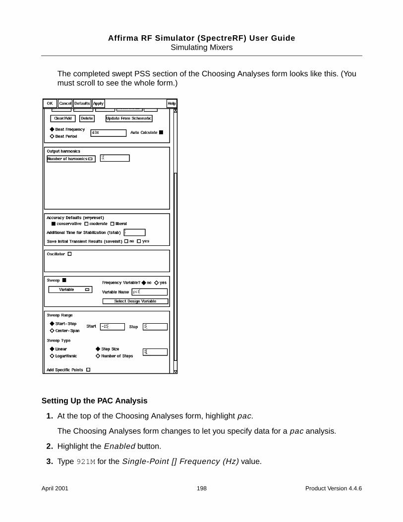
Affirma RF Simulator (SpectreRF) User GuideSimulating Mixers
The completed swept PSS section of the Choosing Analyses form looks like this. (Youmust scroll to see the whole form.)
Setting Up the PAC Analysis
1. At the top of the Choosing Analyses form, highlight pac.
The Choosing Analyses form changes to let you specify data for a pac analysis.
2. Highlight the Enabled button.
3. Type 921M for the Single-Point [] Frequency (Hz) value.
April 2001 198 Product Version 4.4.6
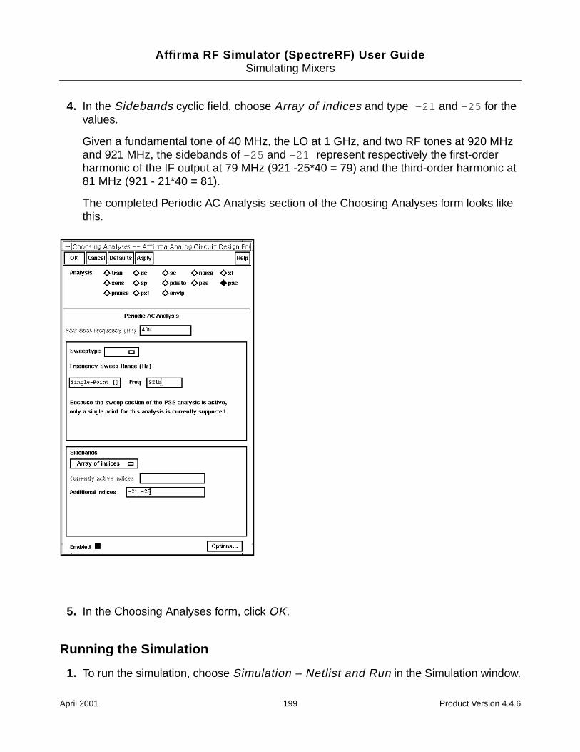
Affirma RF Simulator (SpectreRF) User GuideSimulating Mixers
4. In the Sidebands cyclic field, choose Array of indices and type -21 and -25 for thevalues.
Given a fundamental tone of 40 MHz, the LO at 1 GHz, and two RF tones at 920 MHzand 921 MHz, the sidebands of -25 and -21 represent respectively the first-orderharmonic of the IF output at 79 MHz (921 -25*40 = 79) and the third-order harmonic at81 MHz (921 - 21*40 = 81).
The completed Periodic AC Analysis section of the Choosing Analyses form looks likethis.
5. In the Choosing Analyses form, click OK.
Running the Simulation
1. To run the simulation, choose Simulation – Netlist and Run in the Simulation window.
April 2001 199 Product Version 4.4.6
Affirma RF Simulator (SpectreRF) User GuideSimulating Mixers
Note: This example compares two signals only 1MHz apart. An analysis of two signalsso close together would have taken much longer with the previous analysis.
The output log file appears and displays information about the simulation as it runs.
2. Check the output log file to be sure the simulation is completed successfully.
Plotting the IP3 Curve
In the Simulation window, choose Results – Direct Plot – PSS.
The PSS Results form appears.
In the PSS Results form, do the following:
1. Highlight Replace for Plot Mode.
2. Highlight pac for Analysis Type.
3. Highlight IPN Curves for Function.
4. Choose Variable Sweep (“prf ”) for Circuit Input Power.
5. Type -15 for Extrapolation Point (dBm).
This value is the intercept point for the ideal amplification extrapolation. If you do notspecify a value, the plot defaults to the minimum variable value.
6. Choose Input Referred IP3.
7. Highlight -21 81M in the 3rd Order Harmonic list box.
8. Highlight -25 79M in the 1st Order Harmonic list box.
April 2001 200 Product Version 4.4.6
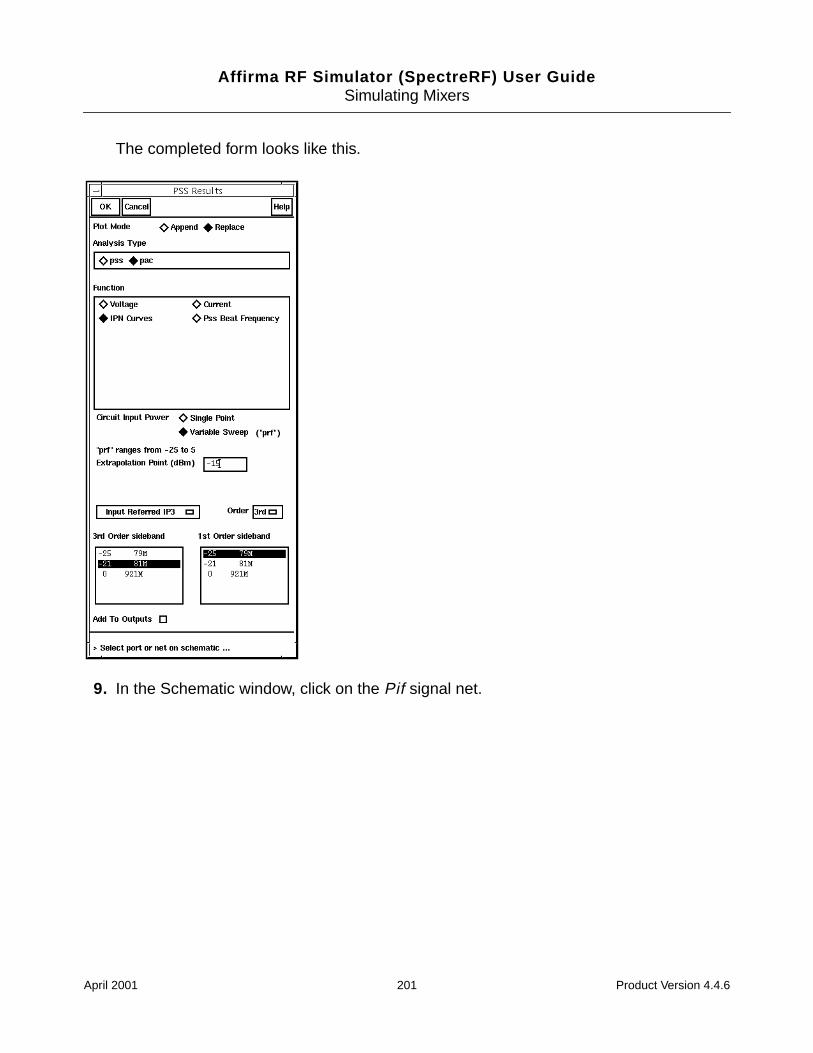
Affirma RF Simulator (SpectreRF) User GuideSimulating Mixers
The completed form looks like this.
9. In the Schematic window, click on the Pif signal net.
April 2001 201 Product Version 4.4.6
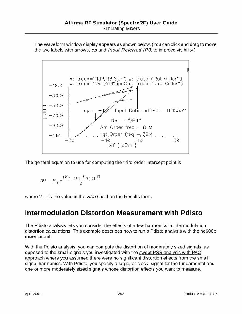
Affirma RF Simulator (SpectreRF) User GuideSimulating Mixers
The Waveform window display appears as shown below. (You can click and drag to movethe two labels with arrows, ep and Input Referred IP3, to improve visibility.)
The general equation to use for computing the third-order intercept point is
where Vrf is the value in the Start field on the Results form.
Intermodulation Distortion Measurement with Pdisto
The Pdisto analysis lets you consider the effects of a few harmonics in intermodulationdistortion calculations. This example describes how to run a Pdisto analysis with the ne600pmixer circuit.
With the Pdisto analysis, you can compute the distortion of moderately sized signals, asopposed to the small signals you investigated with the swept PSS analysis with PACapproach where you assumed there were no significant distortion effects from the smallsignal harmonics. With Pdisto, you specify a large, or clock, signal for the fundamental andone or more moderately sized signals whose distortion effects you want to measure.
IP3 Vrf
Vif 25–( ) Vif 21–( )–( )2
-----------------------------------------------------+=
April 2001 202 Product Version 4.4.6
Affirma RF Simulator (SpectreRF) User GuideSimulating Mixers
Setting Up the Simulation
1. If necessary, open the ne600p mixer circuit.
2. If necessary, specify the full path to the model file in the Model File Set-up form.
3. In the Simulation window, use Analysis - Disable to disable any analyses you ranpreviously. (Check the Simulation window to verify whether or not an analysis isenabled.)
4. If necessary, set the design variables frf to 900Mand flo to 1G. (Check the Simulationwindow to verify the current design variable values.)
Editing the Schematic
In the Schematic window, choose the rf input port and then choose Edit – Properties– Objects.
The Edit Object Properties form for the rf port appears.
In the Edit Object Properties form, do the following:
1. Choose Display small signal params and remove any remaining values from theprevious analysis.
2. Choose sine for Source type.
3. Choose Display second sinusoid and specify the following when the forms changes todisplay new fields:
a. Type fund2 , or any name you choose, in the Frequency name 2 field.
b. Type prf - 10 for the Amplitude 2 (dBm) value.
c. Type 920M for the Frequency 2 value.
4. In the Edit Object Properties form, click OK.
5. In the Schematic window, choose Design – Check and Save.
April 2001 203 Product Version 4.4.6
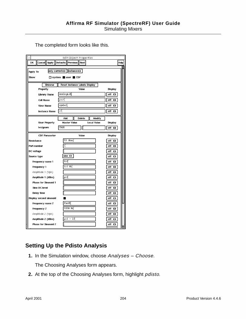
Affirma RF Simulator (SpectreRF) User GuideSimulating Mixers
The completed form looks like this.
Setting Up the Pdisto Analysis
1. In the Simulation window, choose Analyses – Choose.
The Choosing Analyses form appears.
2. At the top of the Choosing Analyses form, highlight pdisto.
April 2001 204 Product Version 4.4.6
Affirma RF Simulator (SpectreRF) User GuideSimulating Mixers
The form changes to let you specify information for the Pdisto analysis. There are threetones in the Fundamental Tones list box, two that were present in the originalspecifications and one that you added.
To update the fundamental tones, perform the following steps:
1. In the Fundamental Tones list box, click on the tone named frf . The tone and itsassociated values appear in the fields below the list box.
2. In the Harms data entry field, type 2 to specify the range of harmonics.
3. Repeat steps 1 and 2 for the fundamental tone named fund2 (or whatever name yougave it).
4. In the Fundamental Tones list box, click on the tone named flo . Choose Large from theSignal cyclic field placed among the fields. In addition, type 1 for the Harms field value.
By choosing Large as the Signal value, you specify flo to be the large or clock signal.Each Pdisto analysis must have one tone set to be the large signal. When you choose asignal for the large signal, choose a tone that is larger, less sinusoidal, or more nonlinearthan the other tones.
Note: You must choose at least one harmonic for each signal that you want to include ina Pdisto analysis. A signal with no harmonics chosen is ignored by the simulation.
In the Choosing Analyses form, do the following:
1. Highlight moderate for the Accuracy Defaults (errpreset) value.
2. Be sure the Enabled button is highlighted.
April 2001 205 Product Version 4.4.6
Affirma RF Simulator (SpectreRF) User GuideSimulating Mixers
The completed form appears like the one below.
3. In the Choosing Analyses form, click OK.
Selecting Simulation Outputs
1. In the Simulation window, choose Outputs – To Be Saved – Select on Schematic.
If you want to plot current or power at the end of the simulation, you must explicitly savethe currents necessary for the calculations. The most economical way to do this, in termsof simulation time, is to choose specific currents on the schematic.
2. In the Schematic window, click on the appropriate terminals to choose rf and rif.
April 2001 206 Product Version 4.4.6
Affirma RF Simulator (SpectreRF) User GuideSimulating Mixers
The terminals are circled in the Schematic window after you choose them.
The selected terminals also appear in the Simulation window.
Running the Simulation
1. To run the simulation, choose Simulation – Netlist and Run in the Simulation window.
The output log file appears and displays information about the simulation as it runs.
2. Check the CIW for a message that says the simulation completed successfully.
Note: Pdisto sends less information to the output log than most other SpectreRF
Selected Terminals
April 2001 207 Product Version 4.4.6
Affirma RF Simulator (SpectreRF) User GuideSimulating Mixers
analyses. While Pdisto is running for this analysis, there might be periods of severalminutes during which there are no messages. This does not mean that the simulation isnot progressing.
Plotting the Voltage and Power
In the Simulation window, choose Results – Direct Plot – PDISTO.
The Pdisto Results form and the Waveform window appear.
In the Pdisto Results form, do the following:
1. Highlight Replace for Plot Mode.
2. Highlight pdisto for Analysis Type.
3. Highlight Voltage for Function.
4. Highlight dB20 for Modifier.
The completed form looks like this.
April 2001 208 Product Version 4.4.6
Affirma RF Simulator (SpectreRF) User GuideSimulating Mixers
5. In the Schematic window, click on the rf terminal that you previously chose to save thecurrent.
The voltage plot for the rf terminal appears.
Because this is a down-converting mixer, the cluster of frequencies from 20 M to 120 Mnear the Y axis of the plot are of interest. To find a frequency and its associated voltage,place the cursor at the tip of a line. The X and Y values that represent the frequency andthe voltage, respectively, appear at the top left corner of the Waveform window. If youplace the cursor at the points shown above, you display the following voltage andfrequency values:
Difference Translation Frequency Voltage
920M - 900M 20M -100.2V
1G - 920M 80M -129V
1G - 900M 100M -119V
X and Yvalues
Placements ofcursor
April 2001 209 Product Version 4.4.6
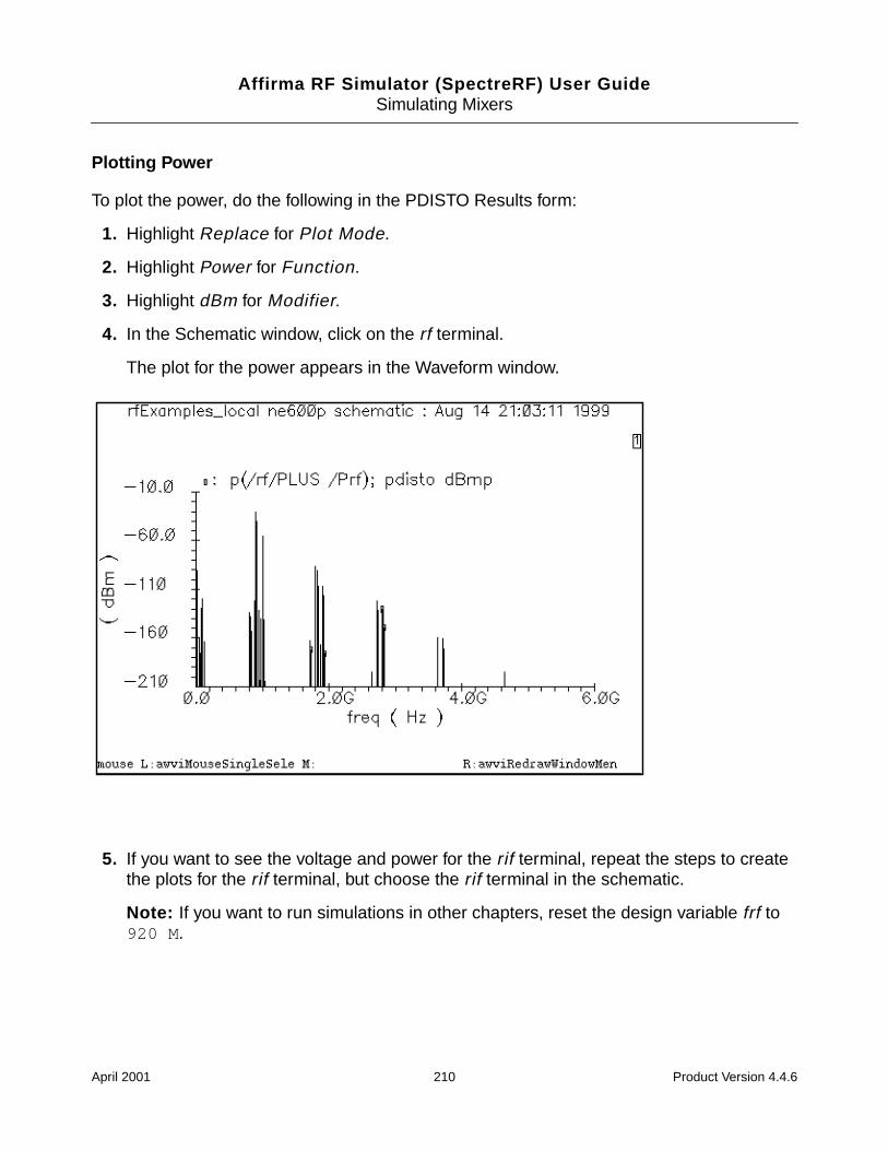
Affirma RF Simulator (SpectreRF) User GuideSimulating Mixers
Plotting Power
To plot the power, do the following in the PDISTO Results form:
1. Highlight Replace for Plot Mode.
2. Highlight Power for Function.
3. Highlight dBm for Modifier.
4. In the Schematic window, click on the rf terminal.
The plot for the power appears in the Waveform window.
5. If you want to see the voltage and power for the rif terminal, repeat the steps to createthe plots for the rif terminal, but choose the rif terminal in the schematic.
Note: If you want to run simulations in other chapters, reset the design variable frf to920 M .
April 2001 210 Product Version 4.4.6
Affirma RF Simulator (SpectreRF) User GuideSimulating Mixers
Noise Figure with Pdisto and QPnoise
You can combine a Pdisto analysis with a small-signal QPnoise analysis to determine thedegradation of the noise figure for the ne600p mixer circuit caused by the two interferingsignals present at the input of the mixer. The noise figure for the ne600p mixer without theinterferer signals is determined in “Noise Figure Measurement with PSS and Pnoise” onpage 160. The Pdisto and QPnoise analyses described in this example include the interferersignals which allow more noise foldings to occur into the output IF band.
The Quasi-Periodic Noise, or QPnoise analysis, is similar to the conventional noise analysis,except that it includes frequency conversion and intermodulation effects. Hence is it useful forpredicting the noise behavior of mixers, switched-capacitor filters, and other periodically orquasi-periodically driven circuits.
Setting Up the Simulation
1. If necessary, open the ne600p mixer circuit.
2. If necessary, specify the full path to the model file in the Model File Set-up form.
3. In the Simulation window, use Analysis - Disable to disable any analyses you ranpreviously. (Check the Simulation window to verify whether or not an analysis isenabled.)
4. If necessary, set the design variables frf to 900Mand flo to 1G. (Check the Simulationwindow to verify the current design variable values.)
Editing the Schematic
1. In the Schematic window, click on the rf input port and then choose Edit – Properties– Objects.
The Edit Object Properties form for the rf input port appears. You use this form to changethe list of CDF properties and modify the schematic for this simulation.
In the Edit Object Properties form, do the following:
1. Choose Display small signal params and remove any remaining values from theprevious analysis.
2. Since the rf signal is moderate signal, choose sine for Source type.
3. Choose Display second sinusoid and specify the following when the forms changes todisplay new fields:
April 2001 211 Product Version 4.4.6
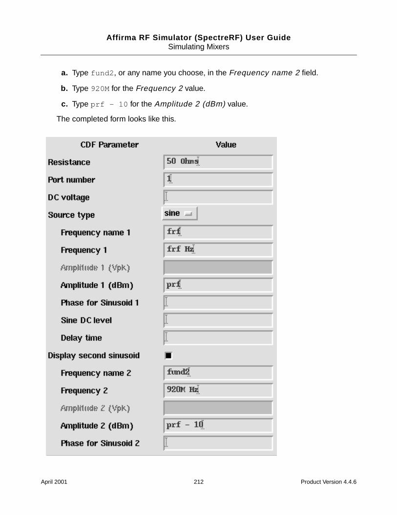
Affirma RF Simulator (SpectreRF) User GuideSimulating Mixers
a. Type fund2 , or any name you choose, in the Frequency name 2 field.
b. Type 920M for the Frequency 2 value.
c. Type prf - 10 for the Amplitude 2 (dBm) value.
The completed form looks like this.
April 2001 212 Product Version 4.4.6
Affirma RF Simulator (SpectreRF) User GuideSimulating Mixers
4. In the Edit Object Properties form, click OK.
5. In the Schematic window, choose Design – Check and Save.
Setting Up the Pdisto and QPnoise Analyses
In the Choosing Analyses form, set up two analyses, first pdisto (qpss) then qpnoise.
In the Simulation window, choose Analyses – Choose.
The Choosing Analyses form appears.
Setting Up the Pdisto Analysis
1. At the top of the Choosing Analyses form, highlight pdisto.
The form changes to let you specify information for the Pdisto analysis.
2. In the Fundamental Tones list box, highlight the tone named frf .
The frf tone and its associated values appear in the fields below the list box.
3. If necessary, choose Moderate from the Signal cyclic field.
4. In the Harms data entry field, highlight the current value and then type 2 to specify therange of harmonics for the frf tone. Any increase in the harmonic range for a moderatetone directly increases the simulation run time.
5. In the list box, highlight the tone named fund2 .
The new values for frf display in the list box. The fund2 tone and its associated valuesappear in the fields below the list box.
6. If necessary, choose Moderate from the Signal cyclic field.
7. In the Harms data entry field, highlight the current value and then type 2 to specify therange of harmonics for the fund2 tone.
8. In the list box, highlight the tone named flo .
The new values for fund2 display in the list box. The flo tone and its associated valuesappear in the fields below the list box.
9. Choose Large from the Signal cyclic field. In addition, highlight the current value in theHarms field and type 5 to specify the range of harmonics for the flo tone. Click Clear/Add.
April 2001 213 Product Version 4.4.6

Affirma RF Simulator (SpectreRF) User GuideSimulating Mixers
The new values for flo display in the list box. The harmonic range of 5 gives 11harmonics (-5, ... ,0, ... +5) for the large tone. Entering a large Harms value for the largetone does not affect the simulation run time.
By choosing Large as the Signal value, you specify flo to be the large or clock signal.Each pdisto analysis must have one tone set to be the large signal. When you choose alarge signal, select a tone that is larger, less sinusoidal, or more nonlinear than the othertones.
You must choose at least one harmonic for each signal that you want to include in apdisto analysis. A signal with a harmonic range value of 0 is ignored by the simulation.In general,
The harmonic range (Harms) value for the Large tone should be at least 5,guaranteeing 11 harmonics.
The Harms value for Moderate tones should be approximately 2 or 3. ForModerate tones, increasing the Harms value increases the simulation run time.
When, as in this example, you specify Harms values of 5 for the Large signal and 2 forthe Moderate signals, you get maxharms = [5,2] which gives you 11 harmonics forthe Large tone and 5 harmonics (-2 -1 0 1 2) for the Moderate tone. As a result, you getnoise from 11 x 5 = 55 frequency sidebands. SpectreRF considers all thesecombinations when performing QPnoise calculations.
10. Highlight moderate for the Accuracy Defaults (errpreset) value.
11. Be sure the Enabled button is highlighted.
April 2001 214 Product Version 4.4.6
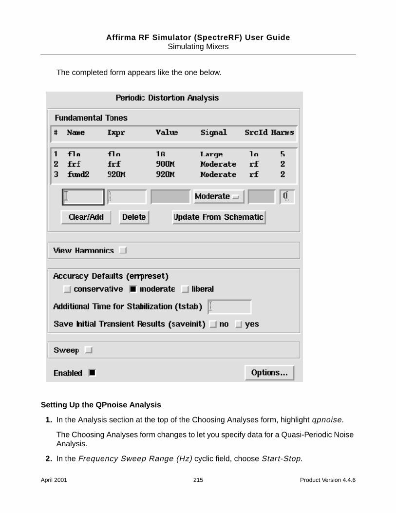
Affirma RF Simulator (SpectreRF) User GuideSimulating Mixers
The completed form appears like the one below.
Setting Up the QPnoise Analysis
1. In the Analysis section at the top of the Choosing Analyses form, highlight qpnoise.
The Choosing Analyses form changes to let you specify data for a Quasi-Periodic NoiseAnalysis.
2. In the Frequency Sweep Range (Hz) cyclic field, choose Start-Stop.
April 2001 215 Product Version 4.4.6
Affirma RF Simulator (SpectreRF) User GuideSimulating Mixers
3. Type 50M and 150M as the Start and Stop values, respectively in the fields.
This frequency range covers the frequencies of interest.
4. In the Sweep Type cyclic field, choose Linear for the sweep type and highlight Numberof Steps. Type 20 for the Number of Steps value in the field.
5. In the Sidebands cyclic field, choose Maximum clock order and type 5.
Maximum clock order is related to large signal harmonics range. A Maximum clockorder of 5 insures that sufficient large-signal harmonics are processed. You can increasethis value.
6. In the Output cyclic field, choose probe for the Output value.
7. Click on the Output Probe Instance Select button. Then click on the appropriatecomponent in the Schematic window to choose Pif.
/rif appears in the Output Probe Instance field.
8. In the Input Source cyclic field, choose port.
9. Click on the Input Port Source Select button. Then click on the appropriate componentin the Schematic window to choose rf.
/rf appears in the Input Port Source field.
10. Type 1 0 0 in the Reference Sideband field. One entry for each tone.
In the Reference Sideband field, enter a vector whose indices have a one-to-onecorrespondence with the fundamental tones. For this example, the correspondence isillustrated in the following table.
The reference sideband vector 1 0 0 mixes with the LO tone only to get the output.
11. Highlight freq for the refsidebandoption.
This selects the frequency as the reference and the reference sideband frequency shiftis computed relative to all combinations of fundamental tones.
Ref Sideband Vector 1 0 0
Fundamental Tones LO FUND2 RF
Frequencies 1 GHz 920 MHz 900 MHz
April 2001 216 Product Version 4.4.6

Affirma RF Simulator (SpectreRF) User GuideSimulating Mixers
When the frequency shift between input and output is calculated, the fundamental tonesare multiplied by the Reference Sideband vector entries and summed. Since differentcombinations might lead to the same frequency shift, refsidebandoption specifies howto perform this calculation.
As in this example, you select freq to calculate frequency shift based on all possiblecombinations.
Select individual when you want to calculate frequency shift based on the onespecified combination only.
12. Be sure the Enabled button is highlighted.
April 2001 217 Product Version 4.4.6
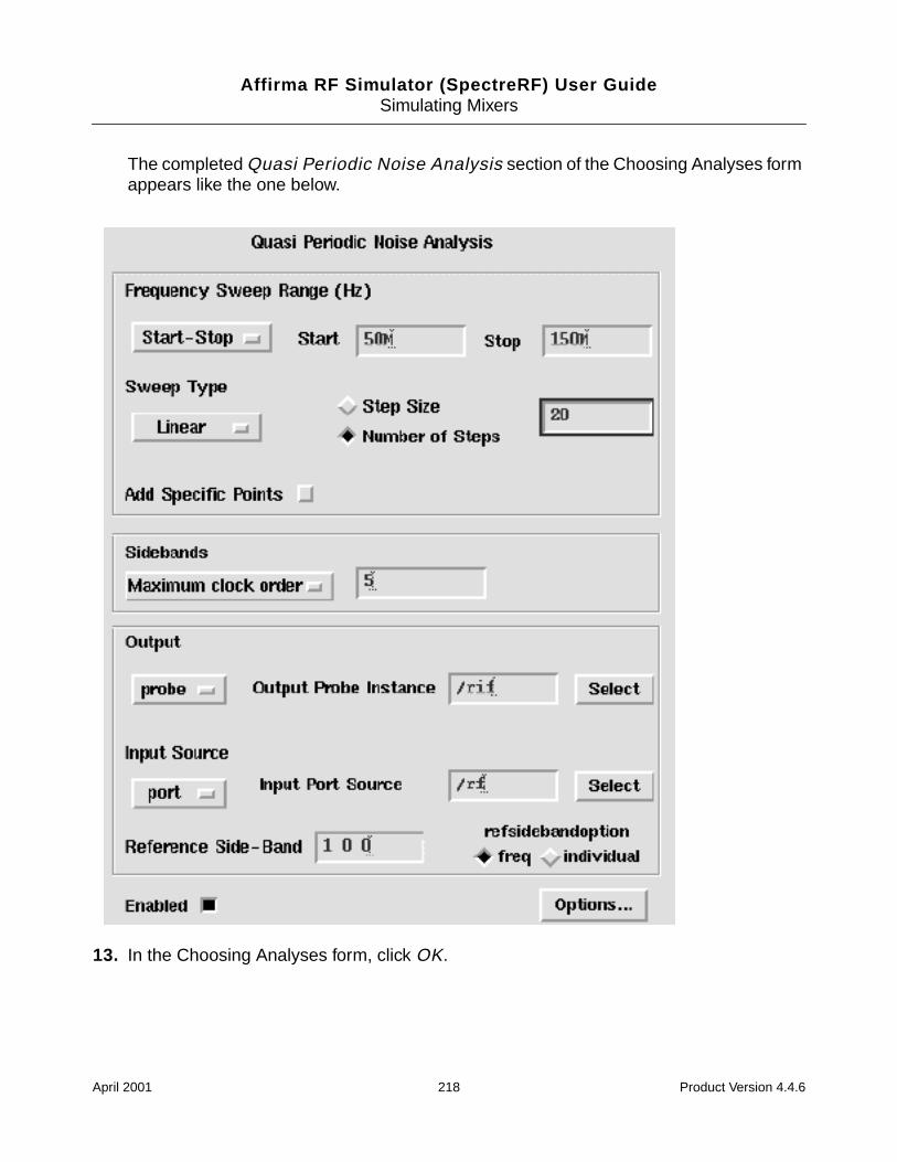
Affirma RF Simulator (SpectreRF) User GuideSimulating Mixers
The completed Quasi Periodic Noise Analysis section of the Choosing Analyses formappears like the one below.
13. In the Choosing Analyses form, click OK.
April 2001 218 Product Version 4.4.6
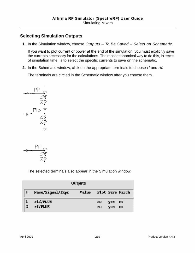
Affirma RF Simulator (SpectreRF) User GuideSimulating Mixers
Selecting Simulation Outputs
1. In the Simulation window, choose Outputs – To Be Saved – Select on Schematic.
If you want to plot current or power at the end of the simulation, you must explicitly savethe currents necessary for the calculations. The most economical way to do this, in termsof simulation time, is to select the specific currents to save on the schematic.
2. In the Schematic window, click on the appropriate terminals to choose rf and rif.
The terminals are circled in the Schematic window after you choose them.
The selected terminals also appear in the Simulation window.
April 2001 219 Product Version 4.4.6
Affirma RF Simulator (SpectreRF) User GuideSimulating Mixers
Running the Simulation
1. To run the simulation, choose Simulation – Netlist and Run in the Simulation window.
The output log file appears and displays information about the simulation as it runs.
2. Check the CIW for a message that says the simulation completed successfully.
Note: Pdisto analysis sends less information to the output log than most otherSpectreRF simulator analyses. While Pdisto is running for this analysis, there might beperiods of several minutes during which there are no messages. This does not mean thatthe simulation is not progressing.
Plotting the Noise Figure
In the Simulation window, choose Results – Direct Plot – PDISTO.
The Pdisto Results form and the Waveform window appear.
In the Pdisto Results form, do the following:
1. Highlight Replace for Plot Mode.
2. Highlight qpnoise for Analysis Type.
3. Highlight Noise Figure for Function.
April 2001 220 Product Version 4.4.6
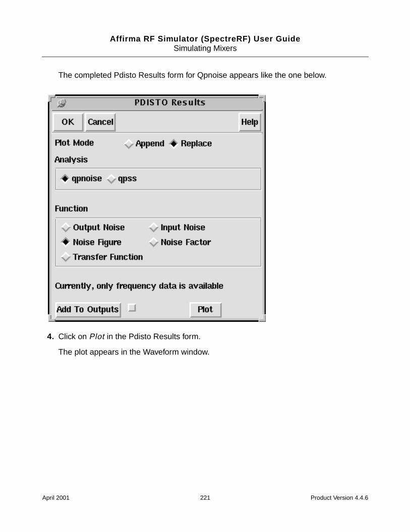
Affirma RF Simulator (SpectreRF) User GuideSimulating Mixers
The completed Pdisto Results form for Qpnoise appears like the one below.
4. Click on Plot in the Pdisto Results form.
The plot appears in the Waveform window.
April 2001 221 Product Version 4.4.6
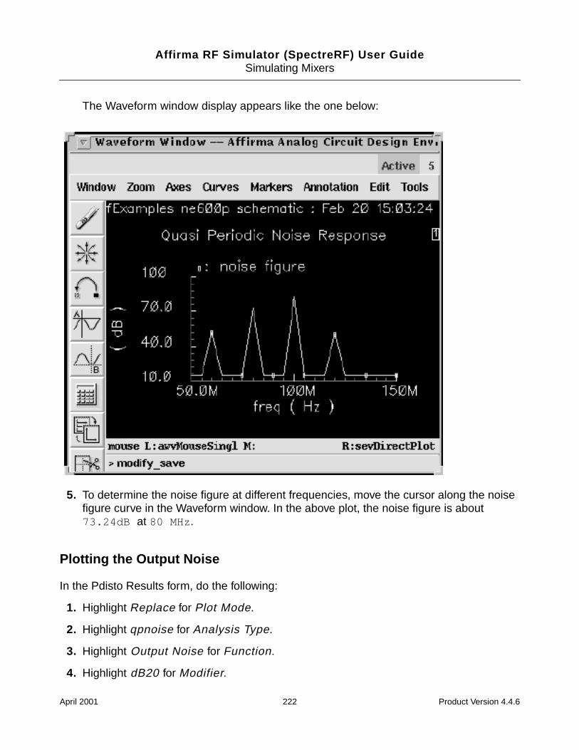
Affirma RF Simulator (SpectreRF) User GuideSimulating Mixers
The Waveform window display appears like the one below:
5. To determine the noise figure at different frequencies, move the cursor along the noisefigure curve in the Waveform window. In the above plot, the noise figure is about73.24dB at 80 MHz .
Plotting the Output Noise
In the Pdisto Results form, do the following:
1. Highlight Replace for Plot Mode.
2. Highlight qpnoise for Analysis Type.
3. Highlight Output Noise for Function.
4. Highlight dB20 for Modifier.
April 2001 222 Product Version 4.4.6
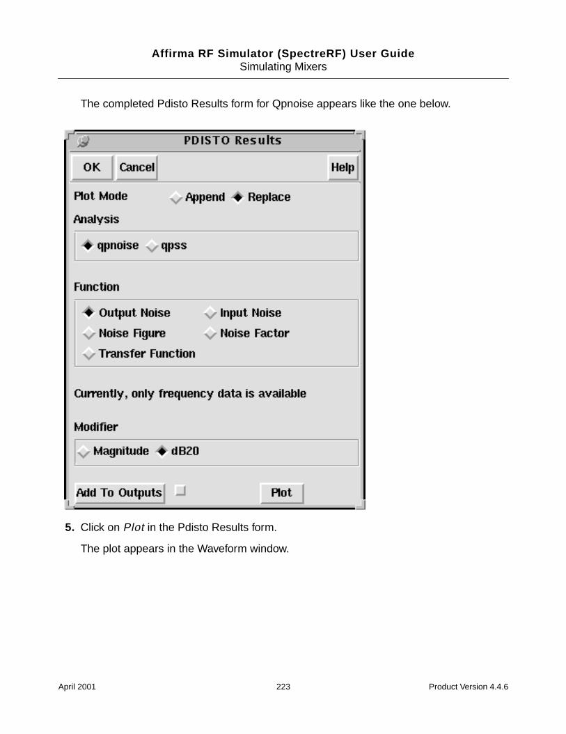
Affirma RF Simulator (SpectreRF) User GuideSimulating Mixers
The completed Pdisto Results form for Qpnoise appears like the one below.
5. Click on Plot in the Pdisto Results form.
The plot appears in the Waveform window.
April 2001 223 Product Version 4.4.6
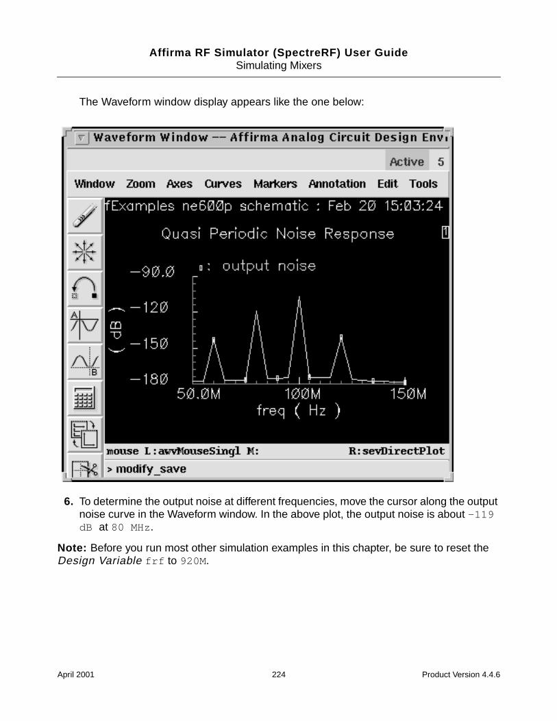
Affirma RF Simulator (SpectreRF) User GuideSimulating Mixers
The Waveform window display appears like the one below:
6. To determine the output noise at different frequencies, move the cursor along the outputnoise curve in the Waveform window. In the above plot, the output noise is about -119dB at 80 MHz .
Note: Before you run most other simulation examples in this chapter, be sure to reset theDesign Variable frf to 920M.
April 2001 224 Product Version 4.4.6
Affirma RF Simulator (SpectreRF) User Guide
5Simulating Oscillators
Autonomous PSS Analysis
Periodic steady state (PSS) analysis lets you simulate both driven and autonomous circuits.Driven circuits, such as amplifiers, filters, or mixers, require a time-varying stimulus to createa time-varying response. Autonomous circuits, such as oscillators, however, have time-varying responses and generate non-constant waveforms even though the circuitsthemselves are time-invariant.
With driven circuits, you specify an analysis period that is an integer multiple of the period ofthe drive signals. You cannot specify the analysis period for autonomous circuits because youdo not know the precise oscillation period in advance. Instead, you specify an estimate of theoscillation period. The PSS analysis uses this estimate to compute the precise period and theperiodic solution waveforms.
To enable PSS analysis to compute the precise period, you specify a pair of nodes. PSSanalysis monitors the potential difference between these nodes and uses this information torefine its estimate of the period.
Phases of Autonomous PSS Anal ysis
A PSS Analysis has two phases, an initial transient analysis phase to initialize the circuit anda shooting phase to compute the periodic steady state solution.
The transient analysis phase is divided into the following three intervals:
A beginning interval that starts at tstart, which is normally 0, and continues through theonset of periodicity for the independent sources
A second, optional stabilization interval of length tstab
A final interval
During this interval, which is four times the estimate of the oscillation period that youspecify in the PSS Analysis form, PSS analysis monitors the waveforms in the circuit andimproves the estimate of the oscillation period.
April 2001 225 Product Version 4.4.6
Affirma RF Simulator (SpectreRF) User GuideSimulating Oscillators
In the shooting phase that follows the transient analysis phase, the circuit is simulatedrepeatedly over one period. The length of the period and the initial conditions are modified tofind the periodic steady state solution.
Phase Noise and Oscillators
Oscillators tend to amplify any noise present near the oscillation frequency. The closer thenoise frequency to the oscillation frequency, the greater the amplification. Noise amplified bythe oscillator in this manner is called phase noise. Phase noise is the most significant sourceof noise in oscillators, and because phase noise is centered about the oscillation frequency,filtering can never completely remove the it.
You can understand phase noise if you recognize that the phase of an oscillator is arbitrarybecause there is no drive signal to lock to. Any waveform that is a solution to an oscillator canbe shifted in time and still be a solution. If a perturbation disturbs the phase, nothing restoresthe phase, so it drifts without bound. If the perturbation is random noise, the drift is a randomwalk. Furthermore, the closer the perturbation frequency is to the oscillation frequency, thebetter it couples to the phase and the greater the drift. The perturbation need not come fromrandom noise. Noise might also couple into the oscillator from other sources, such as thepower supplies.
The two examples in this chapter each examine phase noise.
Starting the Oscillator
When you simulate oscillators using PSS analysis, you must start the oscillator. You can startan oscillator with either of the following techniques:
By supplying a brief impulsive stimulus
The stimulus should couple strongly into the oscillatory mode of the circuit and poorlyinto other long-lasting modes such as bias circuitry.
By supplying initial conditions for the components of the oscillator’s resonator
Stabilizing the Oscillator
With either technique, let the oscillator run long enough to stabilize before starting theshooting phase to compute the steady state solution. Adjust the tstab parameter to supplythe additional stabilization period.
April 2001 226 Product Version 4.4.6
Affirma RF Simulator (SpectreRF) User GuideSimulating Oscillators
About the tline3oscRF Example
This example computes the periodic steady state solution and the phase noise for thetline3oscRF circuit. Phase noise computation is important because phase noise is the mostsignificant source of noise in oscillators. Because phase noise is centered about theoscillation frequency, the noise can never be completely removed by filtering.
The circuit supplies the brief impulsive stimulus needed to start the oscillator, so you do notneed to set initial conditions. You supply the data necessary for PSS analysis to estimate theperiod when you specify the fundamental frequency.
Simulating tline3oscRF
Follow the steps below to simulate the tline3oscRF circuit:
In the Command Interpreter Window (CIW), choose File – Open.
The Open File form appears. Filling in the Open File form lets you open the schematic.
In the Open File form, do the following:
1. Choose rfExamples for Library Name.
2. Choose schematic for View Name.
3. In the Cell Names list box, highlight tline3oscRF. tline3oscRF appears in theCell Name field.
April 2001 227 Product Version 4.4.6
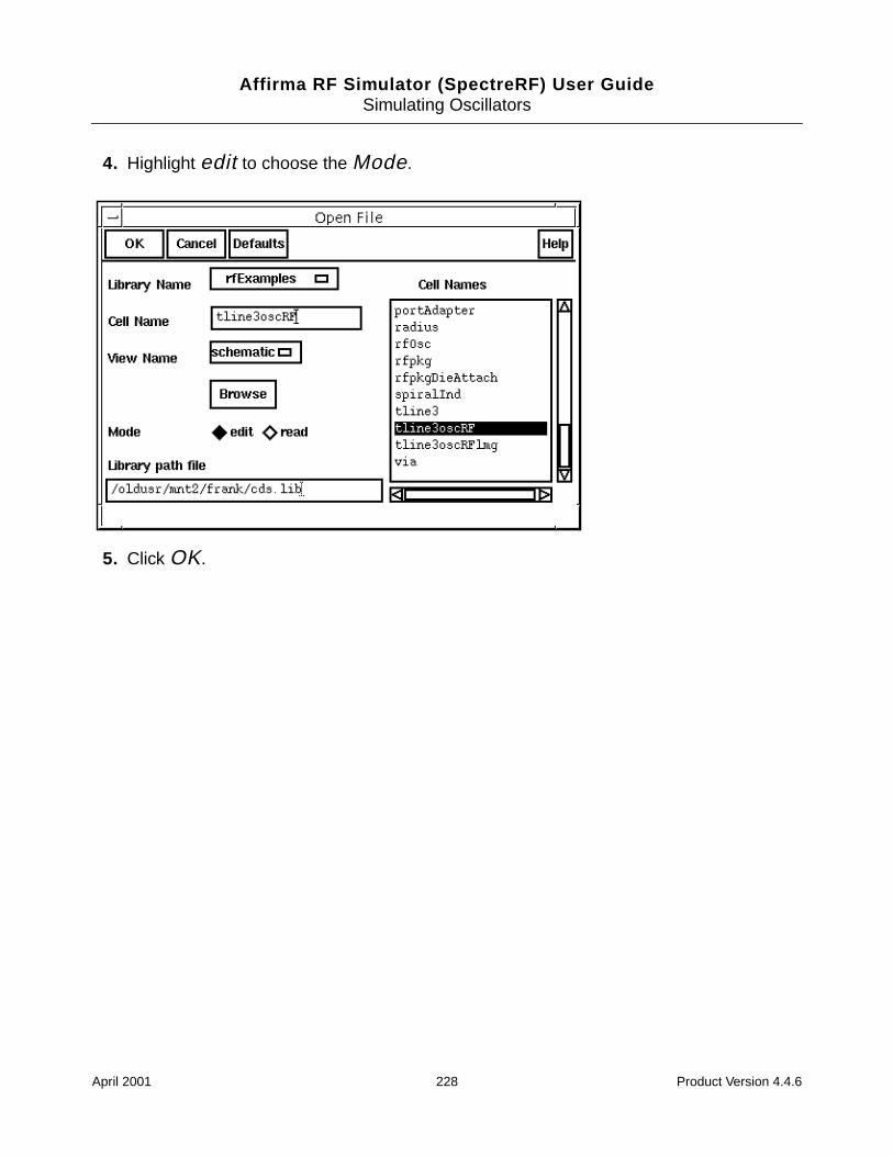
Affirma RF Simulator (SpectreRF) User GuideSimulating Oscillators
4. Highlight edit to choose the Mode.
5. Click OK.
April 2001 228 Product Version 4.4.6
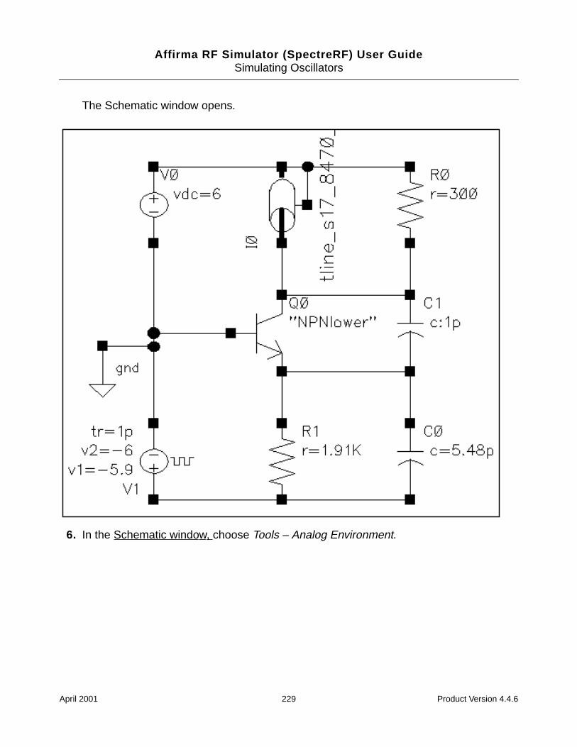
Affirma RF Simulator (SpectreRF) User GuideSimulating Oscillators
The Schematic window opens.
6. In the Schematic window, choose Tools – Analog Environment.
April 2001 229 Product Version 4.4.6
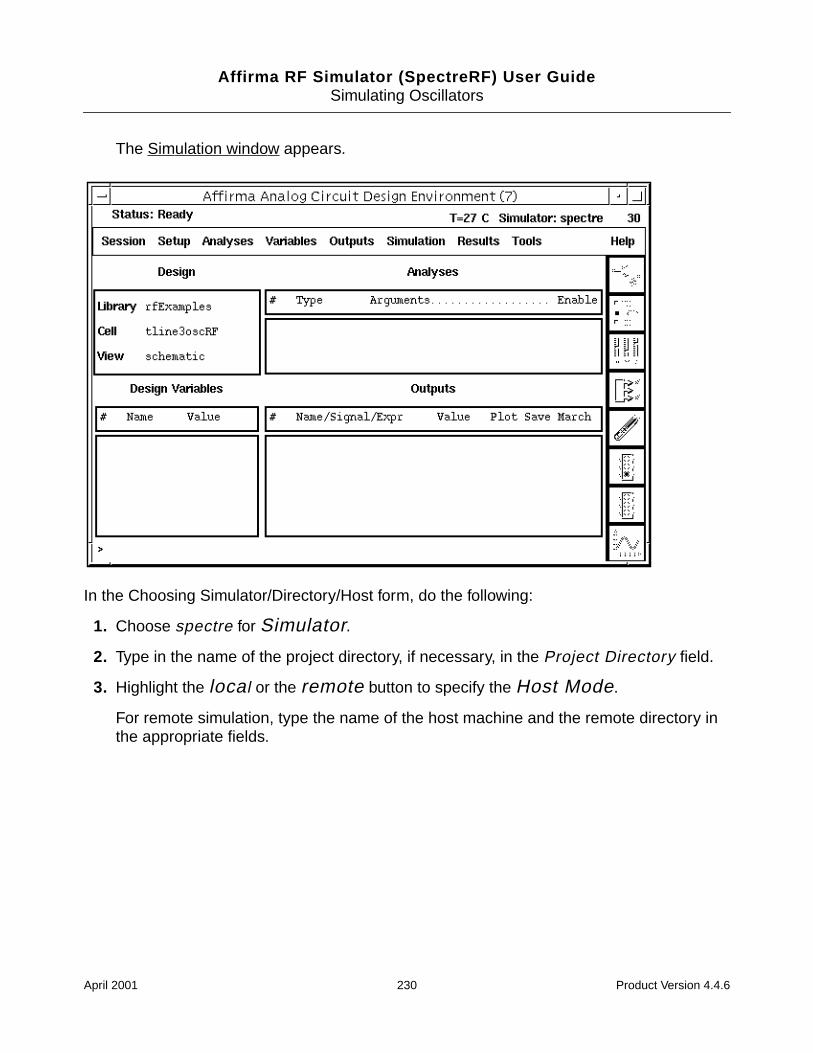
Affirma RF Simulator (SpectreRF) User GuideSimulating Oscillators
The Simulation window appears.
In the Choosing Simulator/Directory/Host form, do the following:
1. Choose spectre for Simulator.
2. Type in the name of the project directory, if necessary, in the Project Directory field.
3. Highlight the local or the remote button to specify the Host Mode.
For remote simulation, type the name of the host machine and the remote directory inthe appropriate fields.
April 2001 230 Product Version 4.4.6
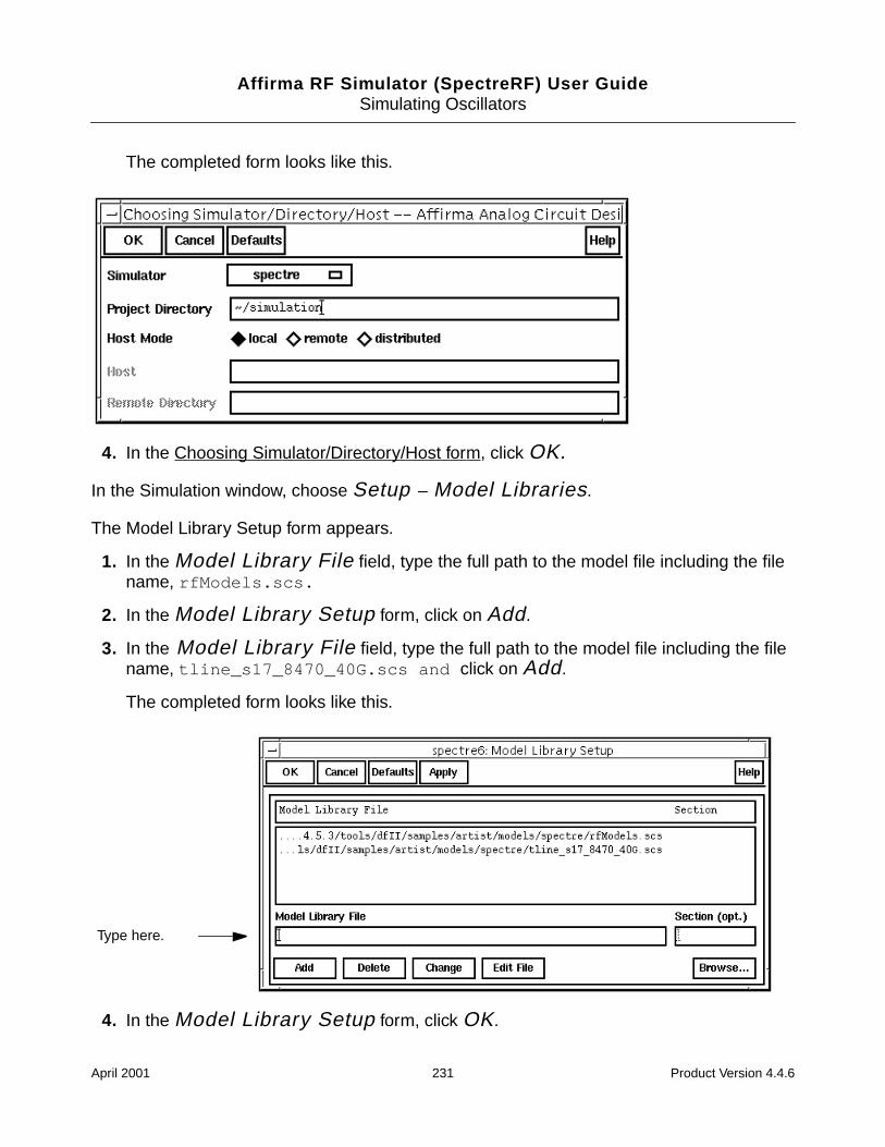
Affirma RF Simulator (SpectreRF) User GuideSimulating Oscillators
The completed form looks like this.
4. In the Choosing Simulator/Directory/Host form, click OK.
In the Simulation window, choose Setup – Model Libraries.
The Model Library Setup form appears.
1. In the Model Library File field, type the full path to the model file including the filename, rfModels.scs.
2. In the Model Library Setup form, click on Add.
3. In the Model Library File field, type the full path to the model file including the filename, tline_s17_8470_40G.scs and click on Add.
The completed form looks like this.
4. In the Model Library Setup form, click OK.
Type here.
April 2001 231 Product Version 4.4.6
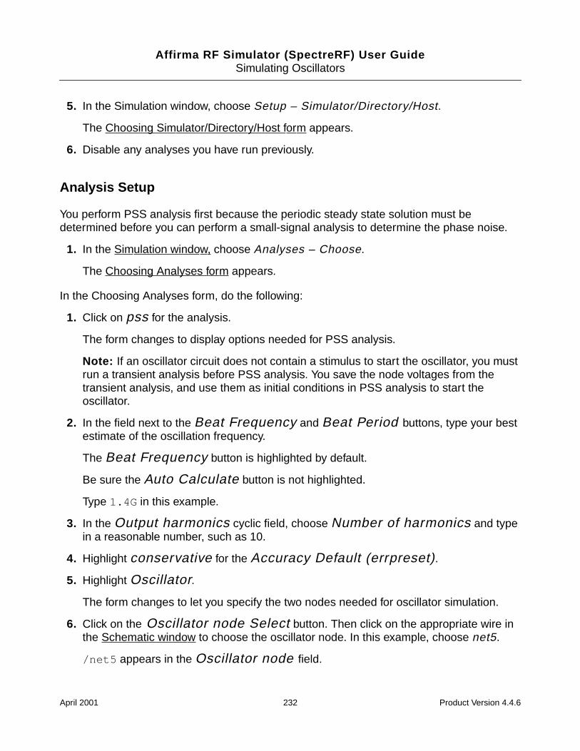
Affirma RF Simulator (SpectreRF) User GuideSimulating Oscillators
5. In the Simulation window, choose Setup – Simulator/Directory/Host.
The Choosing Simulator/Directory/Host form appears.
6. Disable any analyses you have run previously.
Analysis Setup
You perform PSS analysis first because the periodic steady state solution must bedetermined before you can perform a small-signal analysis to determine the phase noise.
1. In the Simulation window, choose Analyses – Choose.
The Choosing Analyses form appears.
In the Choosing Analyses form, do the following:
1. Click on pss for the analysis.
The form changes to display options needed for PSS analysis.
Note: If an oscillator circuit does not contain a stimulus to start the oscillator, you mustrun a transient analysis before PSS analysis. You save the node voltages from thetransient analysis, and use them as initial conditions in PSS analysis to start theoscillator.
2. In the field next to the Beat Frequency and Beat Period buttons, type your bestestimate of the oscillation frequency.
The Beat Frequency button is highlighted by default.
Be sure the Auto Calculate button is not highlighted.
Type 1.4G in this example.
3. In the Output harmonics cyclic field, choose Number of harmonics and typein a reasonable number, such as 10.
4. Highlight conservative for the Accuracy Default (errpreset).
5. Highlight Oscillator.
The form changes to let you specify the two nodes needed for oscillator simulation.
6. Click on the Oscillator node Select button. Then click on the appropriate wire inthe Schematic window to choose the oscillator node. In this example, choose net5.
/net5 appears in the Oscillator node field.
April 2001 232 Product Version 4.4.6
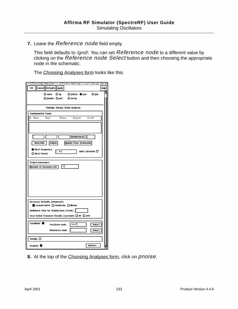
Affirma RF Simulator (SpectreRF) User GuideSimulating Oscillators
7. Leave the Reference node field empty.
This field defaults to /gnd!. You can set Reference node to a different value byclicking on the Reference node Select button and then choosing the appropriatenode in the schematic.
The Choosing Analyses form looks like this.
8. At the top of the Choosing Analyses form, click on pnoise.
April 2001 233 Product Version 4.4.6
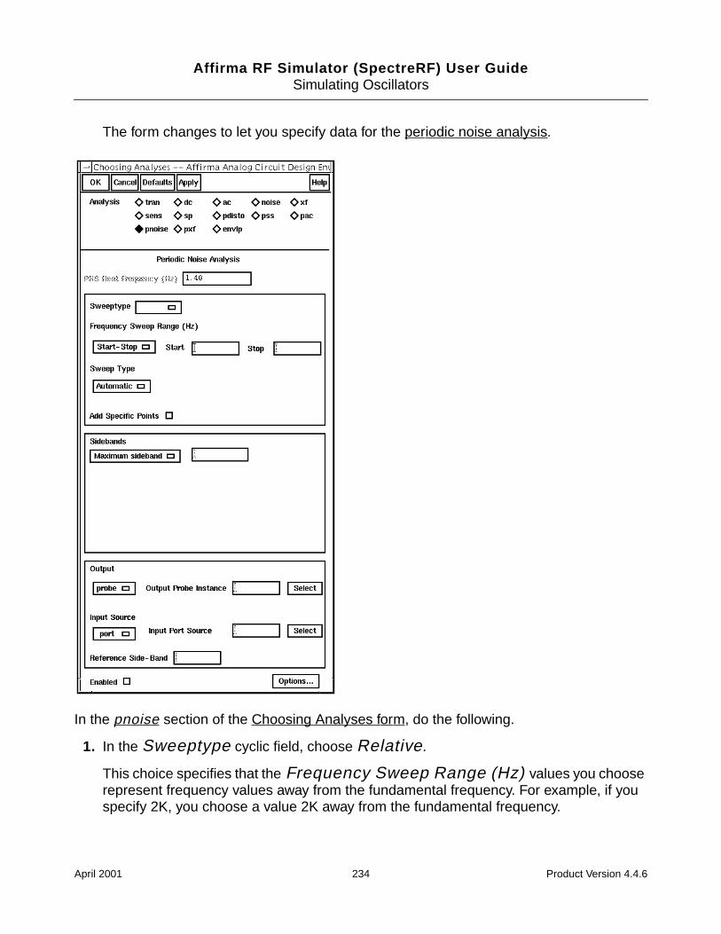
Affirma RF Simulator (SpectreRF) User GuideSimulating Oscillators
The form changes to let you specify data for the periodic noise analysis.
In the pnoise section of the Choosing Analyses form, do the following.
1. In the Sweeptype cyclic field, choose Relative.
This choice specifies that the Frequency Sweep Range (Hz) values you chooserepresent frequency values away from the fundamental frequency. For example, if youspecify 2K, you choose a value 2K away from the fundamental frequency.
April 2001 234 Product Version 4.4.6
Affirma RF Simulator (SpectreRF) User GuideSimulating Oscillators
2. Choose Start-Stop for the type of Frequency Sweep Range (Hz). Type inreasonable values, such as 1K and 100M as the Start and Stop values.
3. In the Sweep Type cyclic field, choose Logarithmic. Use a log sweep when youplot phase noise because of the size of the phase noise values.
4. Highlight Number of Steps, and type 201 in the field.
Note: Be sure to use a nonzero starting value for logarithmic sweeps.
5. In the Sidebands cyclic field, choose Maximum sideband and type 0 in theSidebands field.
6. In the Output cyclic field, choose voltage for the Output choice.
7. Click on the Positive Output Node Select button. Then click on the appropriatewire in the Schematic window to choose net 5.
/net5 appears in the Positive Output Node field.
8. Leave the Negative Output Node field empty.
This field defaults to /gnd!. You can set the Negative Output Node to a differentvalue by clicking on the Negative Output Node Select button and then choosingthe output node in the schematic.
9. In the Input Source cyclic field, choose none.
April 2001 235 Product Version 4.4.6
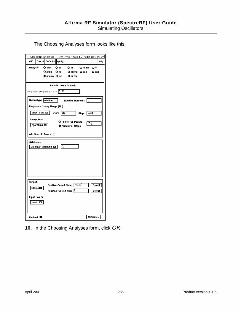
Affirma RF Simulator (SpectreRF) User GuideSimulating Oscillators
The Choosing Analyses form looks like this.
10. In the Choosing Analyses form, click OK.
April 2001 236 Product Version 4.4.6
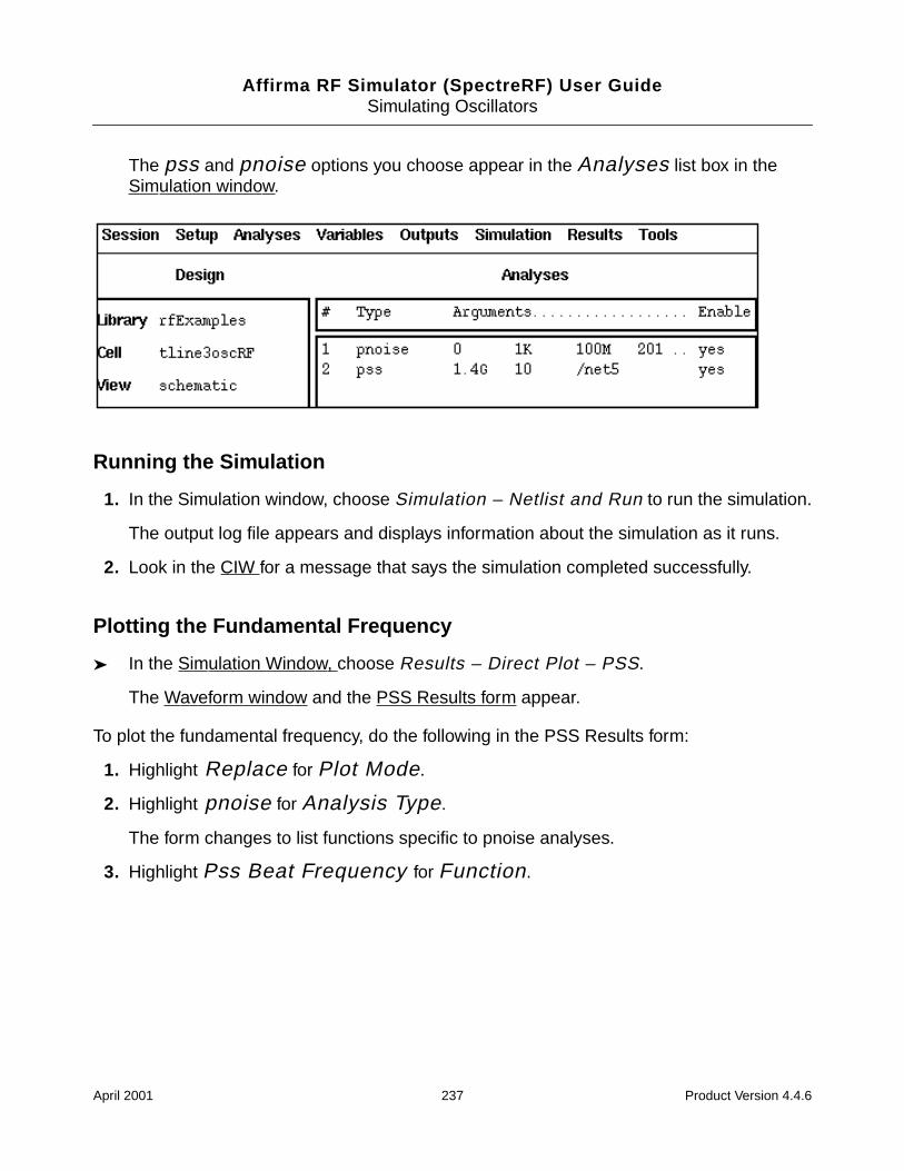
Affirma RF Simulator (SpectreRF) User GuideSimulating Oscillators
The pss and pnoise options you choose appear in the Analyses list box in theSimulation window.
Running the Simulation
1. In the Simulation window, choose Simulation – Netlist and Run to run the simulation.
The output log file appears and displays information about the simulation as it runs.
2. Look in the CIW for a message that says the simulation completed successfully.
Plotting the Fundamental Frequency
In the Simulation Window, choose Results – Direct Plot – PSS.
The Waveform window and the PSS Results form appear.
To plot the fundamental frequency, do the following in the PSS Results form:
1. Highlight Replace for Plot Mode.
2. Highlight pnoise for Analysis Type.
The form changes to list functions specific to pnoise analyses.
3. Highlight Pss Beat Frequency for Function.
April 2001 237 Product Version 4.4.6
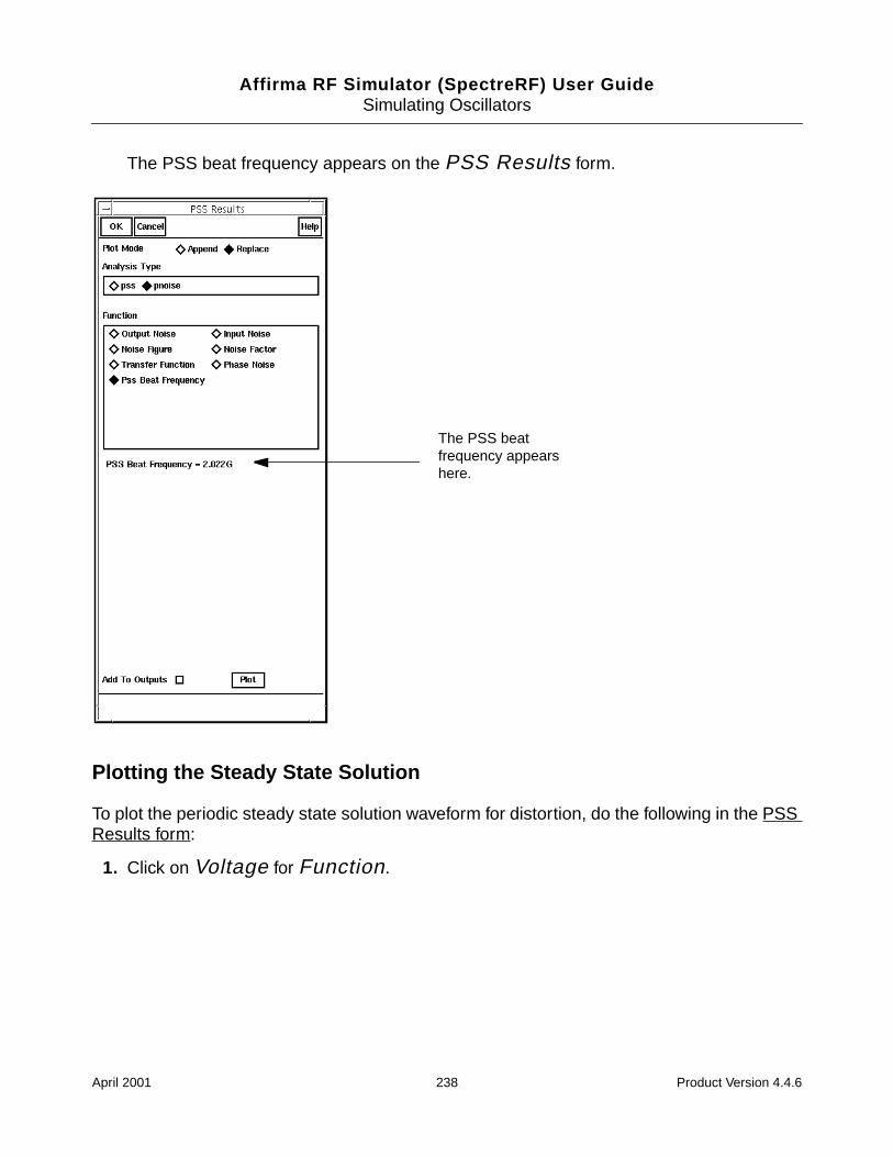
Affirma RF Simulator (SpectreRF) User GuideSimulating Oscillators
The PSS beat frequency appears on the PSS Results form.
Plotting the Steady State Solution
To plot the periodic steady state solution waveform for distortion, do the following in the PSSResults form:
1. Click on Voltage for Function.
The PSS beatfrequency appearshere.
April 2001 238 Product Version 4.4.6
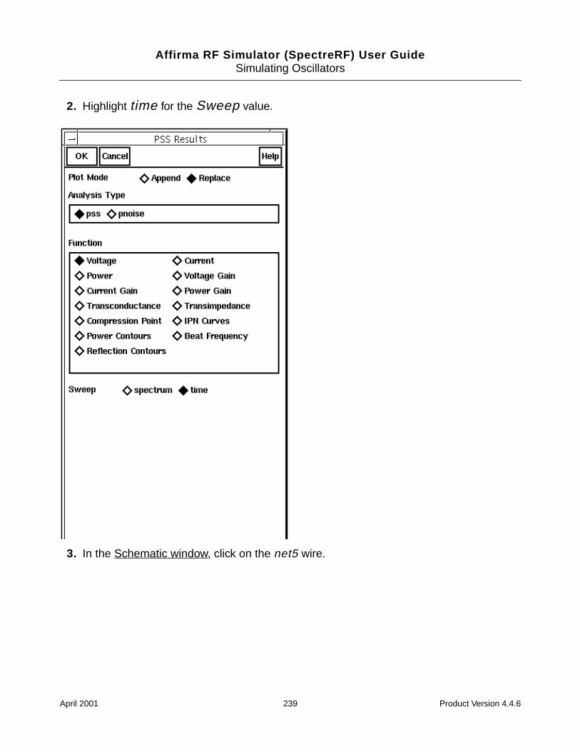
Affirma RF Simulator (SpectreRF) User GuideSimulating Oscillators
2. Highlight time for the Sweep value.
3. In the Schematic window, click on the net5 wire.
April 2001 239 Product Version 4.4.6
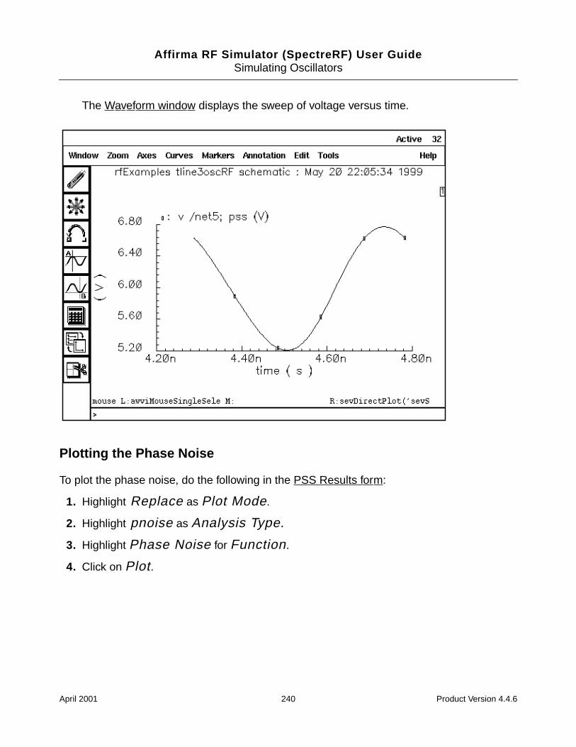
Affirma RF Simulator (SpectreRF) User GuideSimulating Oscillators
The Waveform window displays the sweep of voltage versus time.
Plotting the Phase Noise
To plot the phase noise, do the following in the PSS Results form:
1. Highlight Replace as Plot Mode.
2. Highlight pnoise as Analysis Type.
3. Highlight Phase Noise for Function.
4. Click on Plot.
April 2001 240 Product Version 4.4.6
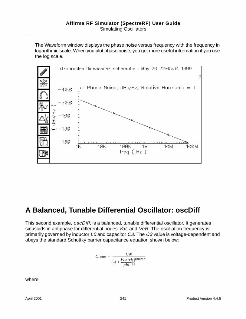
Affirma RF Simulator (SpectreRF) User GuideSimulating Oscillators
The Waveform window displays the phase noise versus frequency with the frequency inlogarithmic scale. When you plot phase noise, you get more useful information if you usethe log scale.
A Balanced, Tunable Differential Oscillator: oscDiff
This second example, oscDiff, is a balanced, tunable differential oscillator. It generatessinusoids in antiphase for differential nodes VoL and VoR. The oscillation frequency isprimarily governed by inductor L0 and capacitor C3. The C3 value is voltage-dependent andobeys the standard Schottky barrier capacitance equation shown below:
where
CtuneCj0
1 Vcntrlphi
----------------+ gamma-------------------------------------------------=
April 2001 241 Product Version 4.4.6
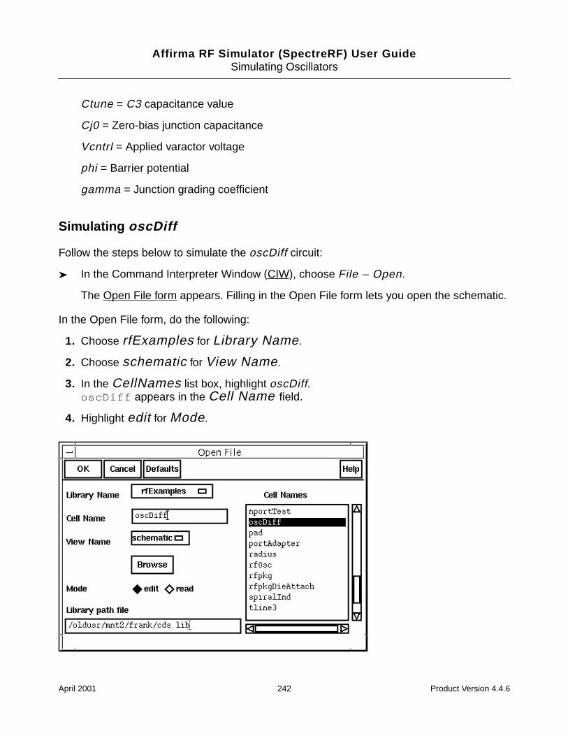
Affirma RF Simulator (SpectreRF) User GuideSimulating Oscillators
Ctune = C3 capacitance value
Cj0 = Zero-bias junction capacitance
Vcntrl = Applied varactor voltage
phi = Barrier potential
gamma = Junction grading coefficient
Simulating oscDiff
Follow the steps below to simulate the oscDiff circuit:
In the Command Interpreter Window (CIW), choose File – Open.
The Open File form appears. Filling in the Open File form lets you open the schematic.
In the Open File form, do the following:
1. Choose rfExamples for Library Name.
2. Choose schematic for View Name.
3. In the CellNames list box, highlight oscDiff.oscDiff appears in the Cell Name field.
4. Highlight edit for Mode.
April 2001 242 Product Version 4.4.6
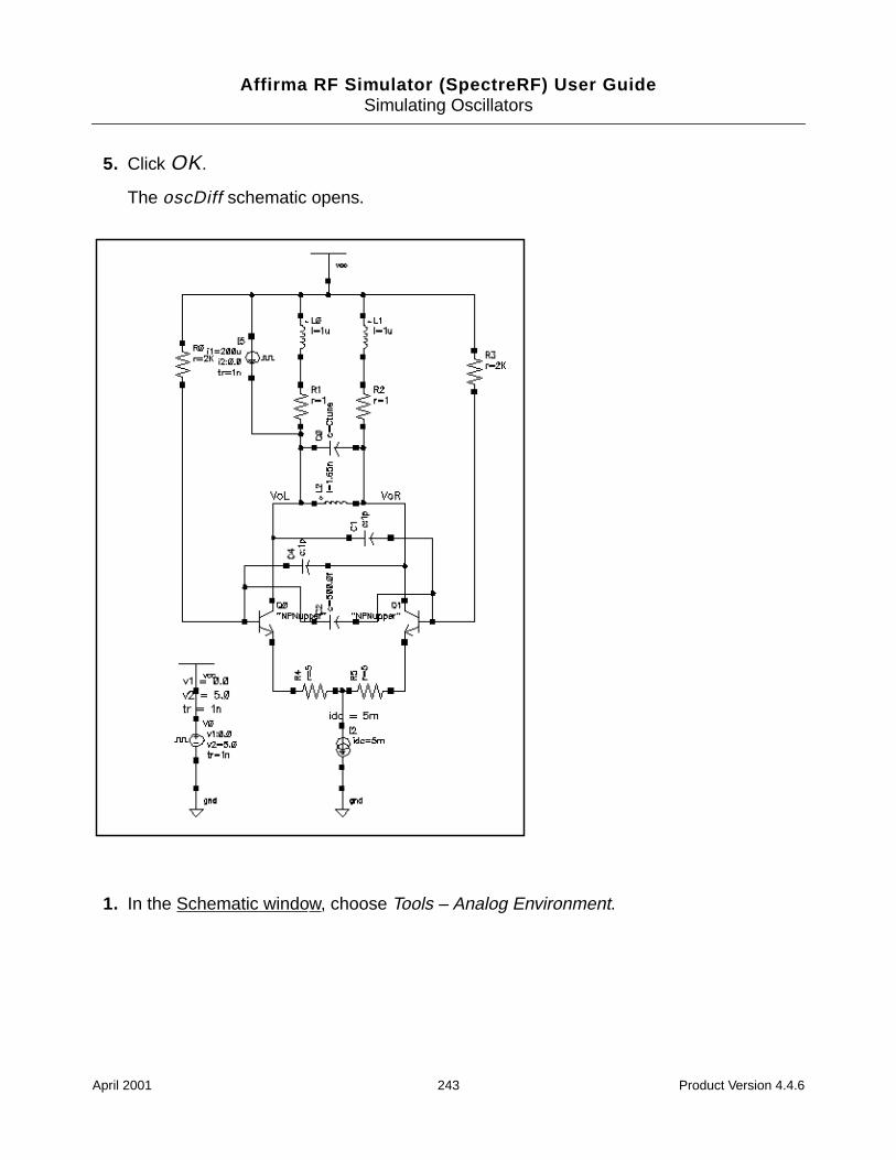
Affirma RF Simulator (SpectreRF) User GuideSimulating Oscillators
5. Click OK.
The oscDiff schematic opens.
1. In the Schematic window, choose Tools – Analog Environment.
April 2001 243 Product Version 4.4.6
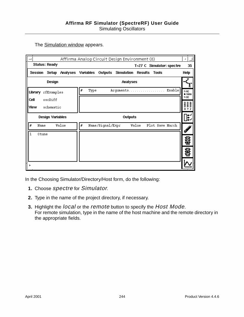
Affirma RF Simulator (SpectreRF) User GuideSimulating Oscillators
The Simulation window appears.
In the Choosing Simulator/Directory/Host form, do the following:
1. Choose spectre for Simulator.
2. Type in the name of the project directory, if necessary.
3. Highlight the local or the remote button to specify the Host Mode.For remote simulation, type in the name of the host machine and the remote directory inthe appropriate fields.
April 2001 244 Product Version 4.4.6
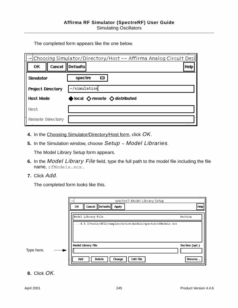
Affirma RF Simulator (SpectreRF) User GuideSimulating Oscillators
The completed form appears like the one below.
4. In the Choosing Simulator/Directory/Host form, click OK.
5. In the Simulation window, choose Setup – Model Libraries.
The Model Library Setup form appears.
6. In the Model Library File field, type the full path to the model file including the filename, rfModels.scs.
7. Click Add.
The completed form looks like this.
8. Click OK.
Type here.
April 2001 245 Product Version 4.4.6
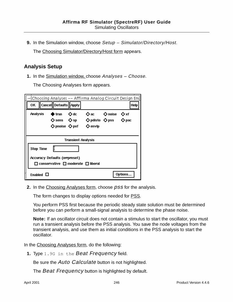
Affirma RF Simulator (SpectreRF) User GuideSimulating Oscillators
9. In the Simulation window, choose Setup – Simulator/Directory/Host.
The Choosing Simulator/Directory/Host form appears.
Analysis Setup
1. In the Simulation window, choose Analyses – Choose.
The Choosing Analyses form appears.
2. In the Choosing Analyses form, choose pss for the analysis.
The form changes to display options needed for PSS.
You perform PSS first because the periodic steady state solution must be determinedbefore you can perform a small-signal analysis to determine the phase noise.
Note: If an oscillator circuit does not contain a stimulus to start the oscillator, you mustrun a transient analysis before the PSS analysis. You save the node voltages from thetransient analysis, and use them as initial conditions in the PSS analysis to start theoscillator.
In the Choosing Analyses form, do the following:
1. Type 1.9G in the Beat Frequency field.
Be sure the Auto Calculate button is not highlighted.
The Beat Frequency button is highlighted by default.
April 2001 246 Product Version 4.4.6
Affirma RF Simulator (SpectreRF) User GuideSimulating Oscillators
2. In the Output harmonics cyclic field, choose Number of harmonics and type5 in the field.
3. Highlight moderate for the Accuracy Default (errpreset).
4. Highlight Oscillator.
The form changes to let you specify the two nodes needed for oscillator simulation.
5. Click on the Oscillator node Select button. Then click on the appropriate wire in theSchematic window to choose the oscillator node. In this example, choose the nodelabelled VoR.
/VoR appears in the Oscillator node field.
6. Click on the Reference node Select button. Then click on the appropriate wire in theSchematic window to choose the oscillator node. In this example, choose the nodelabeled VoL.
/VoL appears in the Reference node field. Because this is a differential oscillator,the reference node is not gnd as it was in the last example.
7. Type 100.5n in the Additional Time for Stabilization (tstab) field.
You can use a slightly different value as long as it is above 100.
8. If you want to save the results of the initial transient analysis, set Save Initial TransientResults (saveinit) to yes.
April 2001 247 Product Version 4.4.6
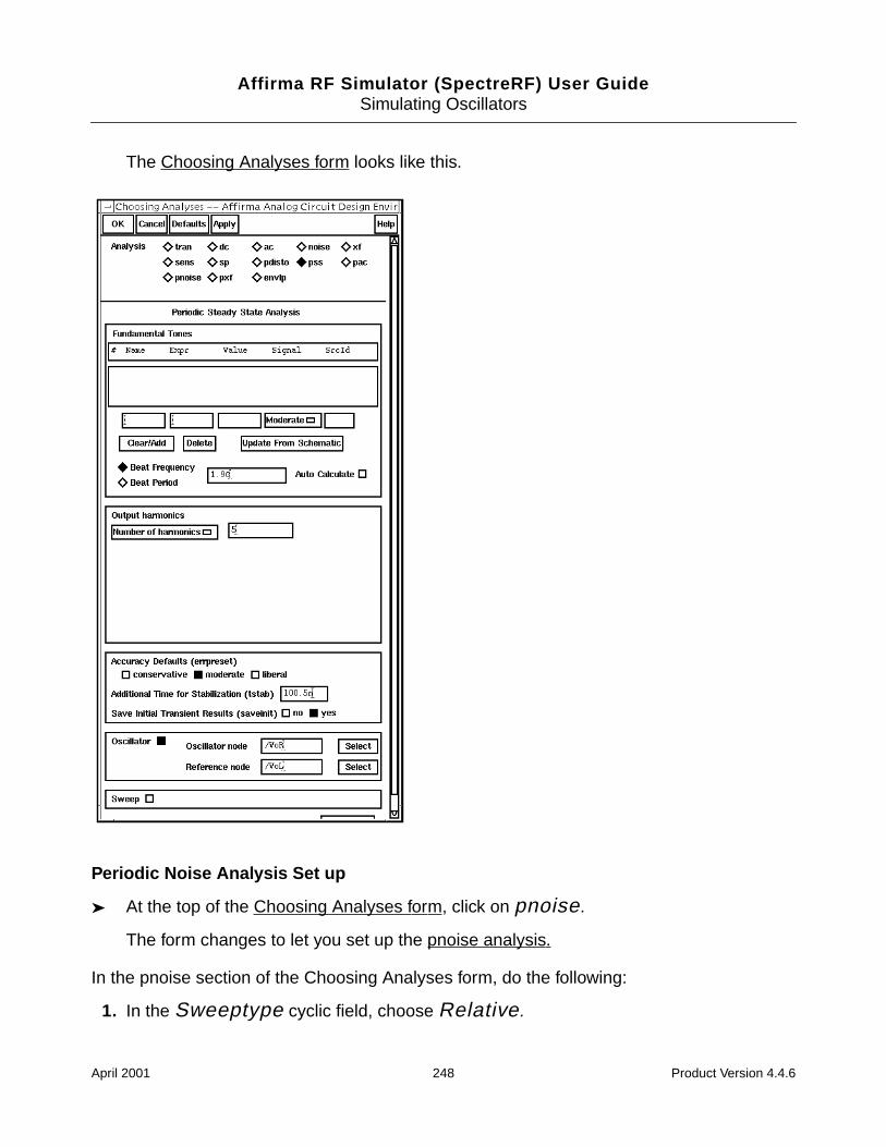
Affirma RF Simulator (SpectreRF) User GuideSimulating Oscillators
The Choosing Analyses form looks like this.
Periodic Noise Analysis Set up
At the top of the Choosing Analyses form, click on pnoise.
The form changes to let you set up the pnoise analysis.
In the pnoise section of the Choosing Analyses form, do the following:
1. In the Sweeptype cyclic field, choose Relative.
April 2001 248 Product Version 4.4.6
Affirma RF Simulator (SpectreRF) User GuideSimulating Oscillators
This choice specifies that the Frequency Sweep Range (Hz) values you chooserepresent frequency values away from the fundamental frequency. For example, if youspecify 2K, you choose a value 2K away from the fundamental frequency.
2. In the Frequency Sweep Range(Hz) cyclic field, choose Start- Stop and type1 and 100M as the Start and Stop values, respectively.
3. In the Sweep Type cyclic field, choose Logarithmic.
Use a log sweep when you plot phase noise because of the size of the phase noisevalues.
4. Highlight Points Per Decade and type 5 in the field.
Note: Be sure to use a nonzero starting value for logarithmic sweeps.
5. In the Sidebands cyclic field, choose Maximum sideband and type 0 in the field.
6. In the Output cyclic field, choose voltage for the Output choice.
7. Click on the Positive Output Node Select button. Then click on the appropriatewire in the Schematic window to choose VoR.
/VoR appears in the Positive Output Node field.
8. Click on the Negative Output Node Select button. Then click on the appropriatewire in the Schematic window to choose VoL.
/VoL appears in the Negative Output Node field. Because this is a differentialoscillator, the negative output node is not gnd as it was for the tline3oscRF oscillator.
9. In the Input Source cyclic field, choose none.
April 2001 249 Product Version 4.4.6
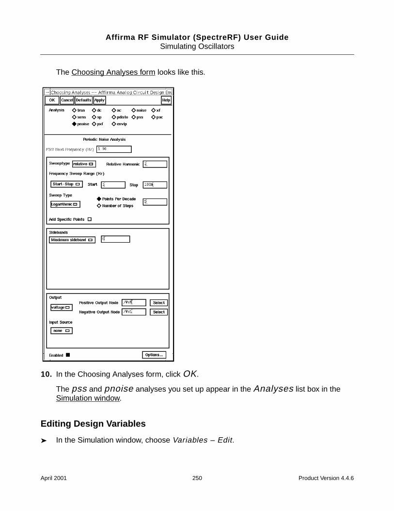
Affirma RF Simulator (SpectreRF) User GuideSimulating Oscillators
The Choosing Analyses form looks like this.
10. In the Choosing Analyses form, click OK.
The pss and pnoise analyses you set up appear in the Analyses list box in theSimulation window.
Editing Design Variables
In the Simulation window, choose Variables – Edit.
April 2001 250 Product Version 4.4.6
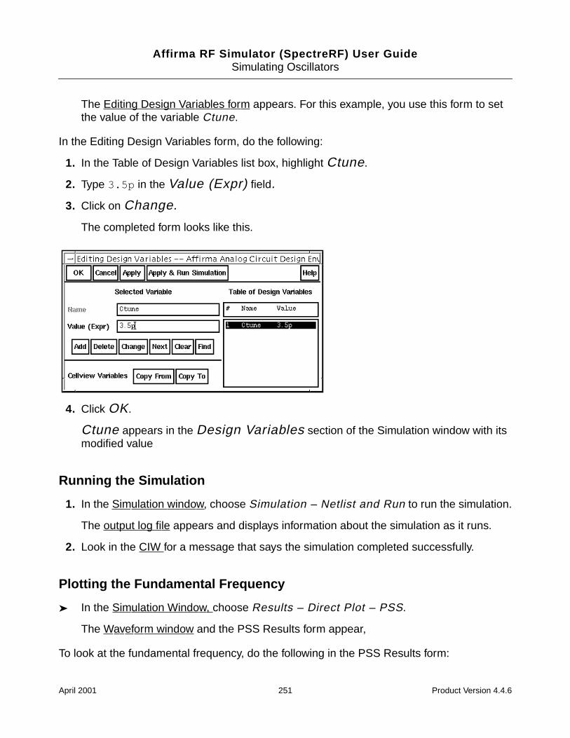
Affirma RF Simulator (SpectreRF) User GuideSimulating Oscillators
The Editing Design Variables form appears. For this example, you use this form to setthe value of the variable Ctune.
In the Editing Design Variables form, do the following:
1. In the Table of Design Variables list box, highlight Ctune.
2. Type 3.5p in the Value (Expr) field.
3. Click on Change.
The completed form looks like this.
4. Click OK.
Ctune appears in the Design Variables section of the Simulation window with itsmodified value
Running the Simulation
1. In the Simulation window, choose Simulation – Netlist and Run to run the simulation.
The output log file appears and displays information about the simulation as it runs.
2. Look in the CIW for a message that says the simulation completed successfully.
Plotting the Fundamental Frequency
In the Simulation Window, choose Results – Direct Plot – PSS.
The Waveform window and the PSS Results form appear,
To look at the fundamental frequency, do the following in the PSS Results form:
April 2001 251 Product Version 4.4.6
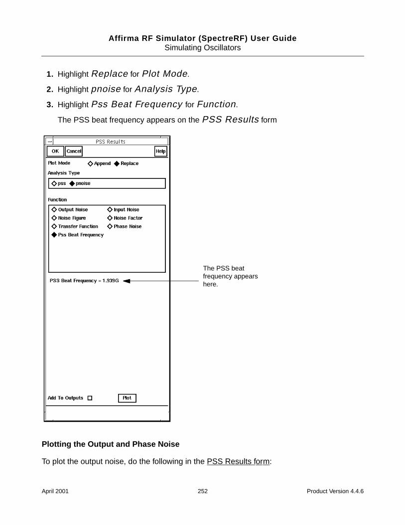
Affirma RF Simulator (SpectreRF) User GuideSimulating Oscillators
1. Highlight Replace for Plot Mode.
2. Highlight pnoise for Analysis Type.
3. Highlight Pss Beat Frequency for Function.
The PSS beat frequency appears on the PSS Results form
Plotting the Output and Phase Noise
To plot the output noise, do the following in the PSS Results form:
The PSS beatfrequency appearshere.
April 2001 252 Product Version 4.4.6
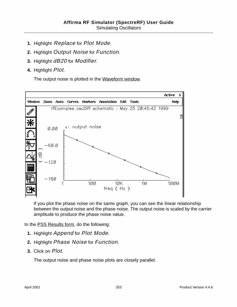
Affirma RF Simulator (SpectreRF) User GuideSimulating Oscillators
1. Highlight Replace for Plot Mode.
2. Highlight Output Noise for Function.
3. Highlight dB20 for Modifier.
4. Highlight Plot.
The output noise is plotted in the Waveform window.
If you plot the phase noise on the same graph, you can see the linear relationshipbetween the output noise and the phase noise. The output noise is scaled by the carrieramplitude to produce the phase noise value.
In the PSS Results form, do the following:
1. Highlight Append for Plot Mode.
2. Highlight Phase Noise for Function.
3. Click on Plot.
The output noise and phase noise plots are closely parallel.
April 2001 253 Product Version 4.4.6
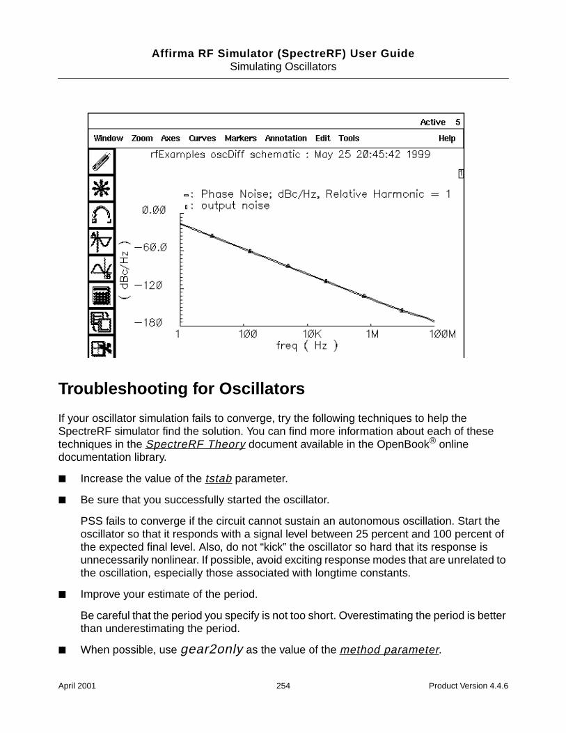
Affirma RF Simulator (SpectreRF) User GuideSimulating Oscillators
Troubleshooting for Oscillators
If your oscillator simulation fails to converge, try the following techniques to help theSpectreRF simulator find the solution. You can find more information about each of thesetechniques in the SpectreRF Theory document available in the OpenBook® onlinedocumentation library.
Increase the value of the tstab parameter.
Be sure that you successfully started the oscillator.
PSS fails to converge if the circuit cannot sustain an autonomous oscillation. Start theoscillator so that it responds with a signal level between 25 percent and 100 percent ofthe expected final level. Also, do not “kick” the oscillator so hard that its response isunnecessarily nonlinear. If possible, avoid exciting response modes that are unrelated tothe oscillation, especially those associated with longtime constants.
Improve your estimate of the period.
Be careful that the period you specify is not too short. Overestimating the period is betterthan underestimating the period.
When possible, use gear2only as the value of the method parameter.
April 2001 254 Product Version 4.4.6
Affirma RF Simulator (SpectreRF) User GuideSimulating Oscillators
Increase the value of the maxperiods parameter to increase the maximum number ofiterations for the shooting methods.
If the shooting iteration approaches convergence and then fails, increase the value of thesteadyratio parameter.
The steadyratio parameter controls how much the final solution can deviate from beingperiodic.
Change the value of the tolerance parameter.
Changing the value of the tolerance parameter does not change the accuracy of thefinal solution, but it increases the chance that the simulation converges.
Tighten the normal simulation tolerances by changing the values of the maxstep, reltol,lteratio, and errpreset parameters. Avoid setting errpreset to liberal.
April 2001 255 Product Version 4.4.6
Affirma RF Simulator (SpectreRF) User Guide
6Simulating Low-Noise Amplifiers
Readers of this chapter must have basic familiarity with the SpectreRF simulator analyses aswell as knowledge about low-noise amplifier design. For more information about theSpectreRF simulator analyses, see Chapter 1, “SpectreRF Analyses.”
Types of Analysis Shown in this Chapter
This chapter shows you how to simulate and plot the following:
Voltage Gain
Output Voltage Distribution
S-Parameter Analysis, including the Voltage Standing Wave Ratio
S-Parameter Noise Analysis, including
Noise Figure and Minimum Noise Figure
Equivalent Noise Resistance
Load and Source Stability Circles
Noise Circles
Noise Figure Calculations with the Pnoise Analysis
The 1dB Compression Point
The Third-Order Intercept Point
Conversion Gain and Power Supply Rejection with the Periodic Transfer FunctionAnalysis
Procedures for Simulating the LNA Example
1. In the Command Interpreter Window (CIW), choose File – Open.
April 2001 256 Product Version 4.4.6
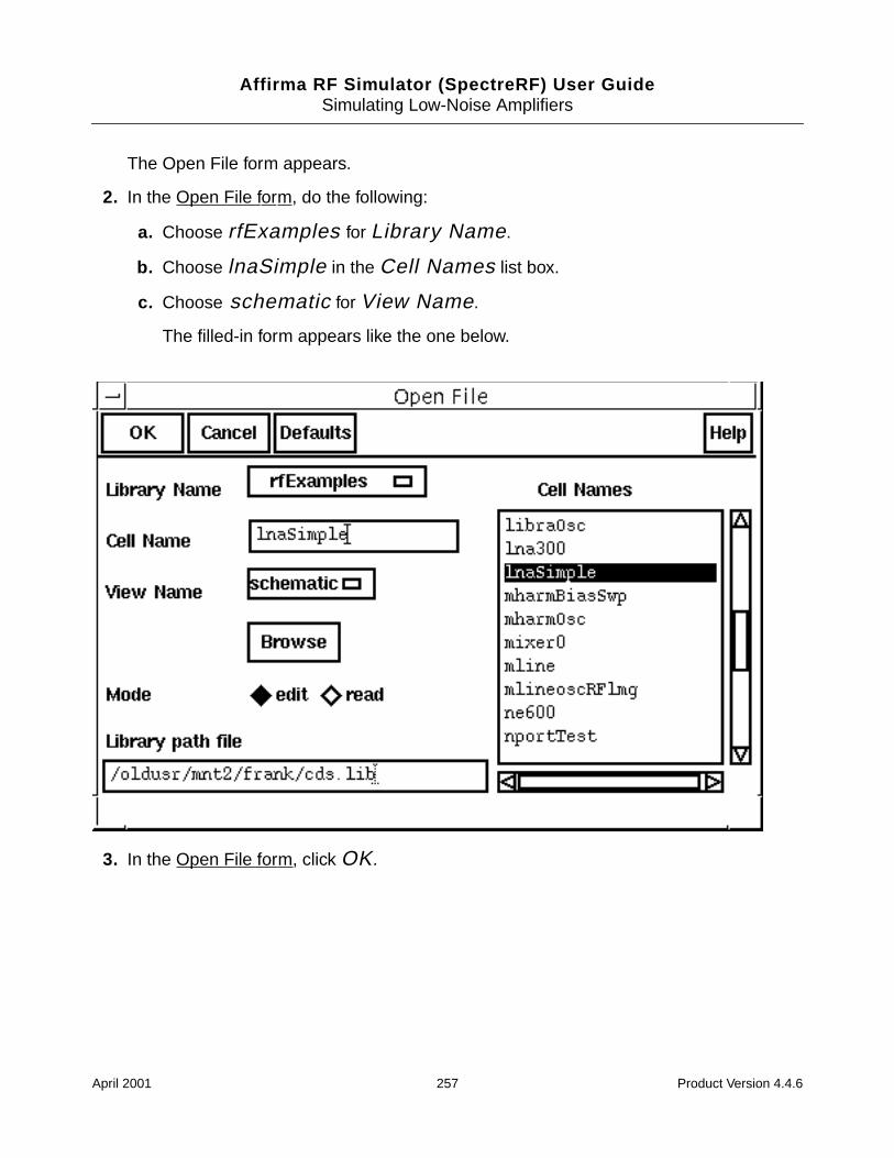
Affirma RF Simulator (SpectreRF) User GuideSimulating Low-Noise Amplifiers
The Open File form appears.
2. In the Open File form, do the following:
a. Choose rfExamples for Library Name.
b. Choose lnaSimple in the Cell Names list box.
c. Choose schematic for View Name.
The filled-in form appears like the one below.
3. In the Open File form, click OK.
April 2001 257 Product Version 4.4.6
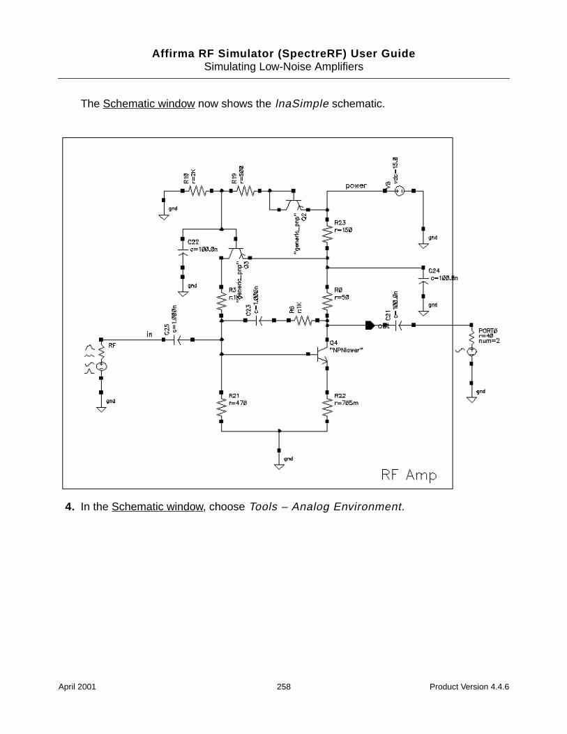
Affirma RF Simulator (SpectreRF) User GuideSimulating Low-Noise Amplifiers
The Schematic window now shows the lnaSimple schematic.
4. In the Schematic window, choose Tools – Analog Environment.
April 2001 258 Product Version 4.4.6
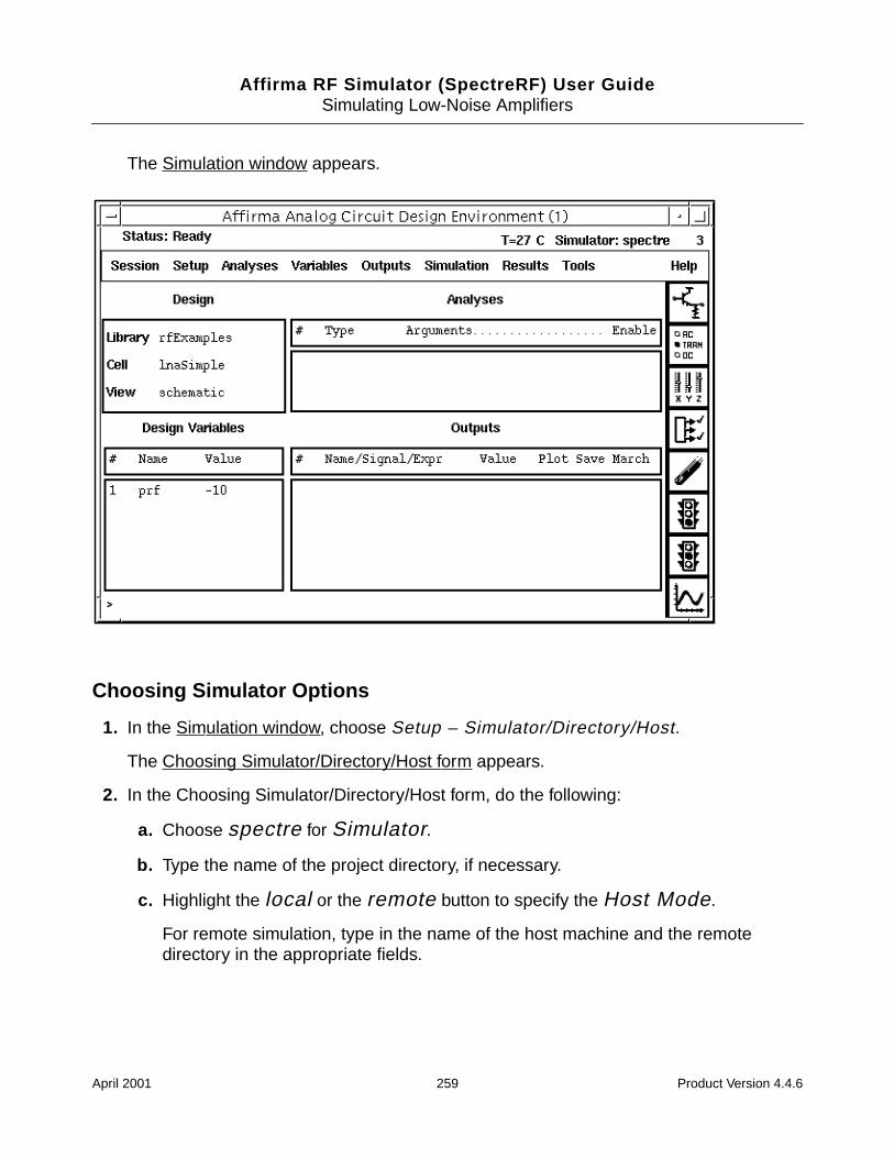
Affirma RF Simulator (SpectreRF) User GuideSimulating Low-Noise Amplifiers
The Simulation window appears.
Choosing Simulator Options
1. In the Simulation window, choose Setup – Simulator/Directory/Host.
The Choosing Simulator/Directory/Host form appears.
2. In the Choosing Simulator/Directory/Host form, do the following:
a. Choose spectre for Simulator.
b. Type the name of the project directory, if necessary.
c. Highlight the local or the remote button to specify the Host Mode.
For remote simulation, type in the name of the host machine and the remotedirectory in the appropriate fields.
April 2001 259 Product Version 4.4.6
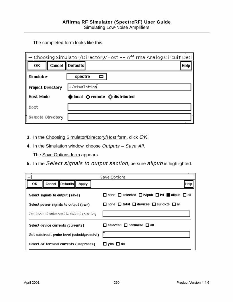
Affirma RF Simulator (SpectreRF) User GuideSimulating Low-Noise Amplifiers
The completed form looks like this.
3. In the Choosing Simulator/Directory/Host form, click OK.
4. In the Simulation window, choose Outputs – Save All.
The Save Options form appears.
5. In the Select signals to output section, be sure allpub is highlighted.
April 2001 260 Product Version 4.4.6
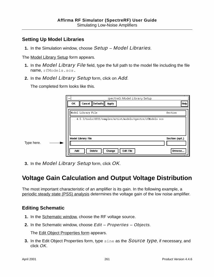
Affirma RF Simulator (SpectreRF) User GuideSimulating Low-Noise Amplifiers
Setting Up Model Libraries
1. In the Simulation window, choose Setup – Model Libraries.
The Model Library Setup form appears.
1. In the Model Library File field, type the full path to the model file including the filename, rfModels.scs.
2. In the Model Library Setup form, click on Add.
The completed form looks like this.
3. In the Model Library Setup form, click OK.
Voltage Gain Calculation and Output Voltage Distribution
The most important characteristic of an amplifier is its gain. In the following example, aperiodic steady state (PSS) analysis determines the voltage gain of the low noise amplifier.
Editing Schematic
1. In the Schematic window, choose the RF voltage source.
2. In the Schematic window, choose Edit – Properties – Objects.
The Edit Object Properties form appears.
3. In the Edit Object Properties form, type sine as the Source type, if necessary, andclick OK.
Type here.
April 2001 261 Product Version 4.4.6
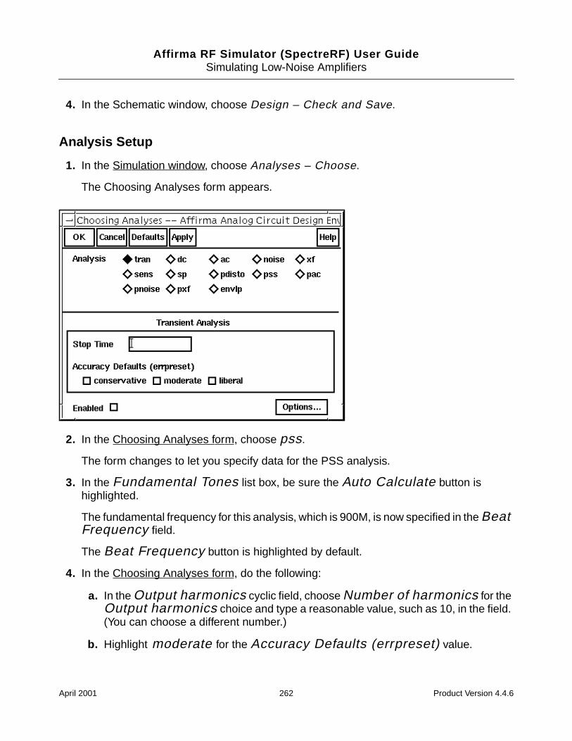
Affirma RF Simulator (SpectreRF) User GuideSimulating Low-Noise Amplifiers
4. In the Schematic window, choose Design – Check and Save.
Analysis Setup
1. In the Simulation window, choose Analyses – Choose.
The Choosing Analyses form appears.
2. In the Choosing Analyses form, choose pss.
The form changes to let you specify data for the PSS analysis.
3. In the Fundamental Tones list box, be sure the Auto Calculate button ishighlighted.
The fundamental frequency for this analysis, which is 900M, is now specified in the BeatFrequency field.
The Beat Frequency button is highlighted by default.
4. In the Choosing Analyses form, do the following:
a. In the Output harmonics cyclic field, choose Number of harmonics for theOutput harmonics choice and type a reasonable value, such as 10, in the field.(You can choose a different number.)
b. Highlight moderate for the Accuracy Defaults (errpreset) value.
April 2001 262 Product Version 4.4.6
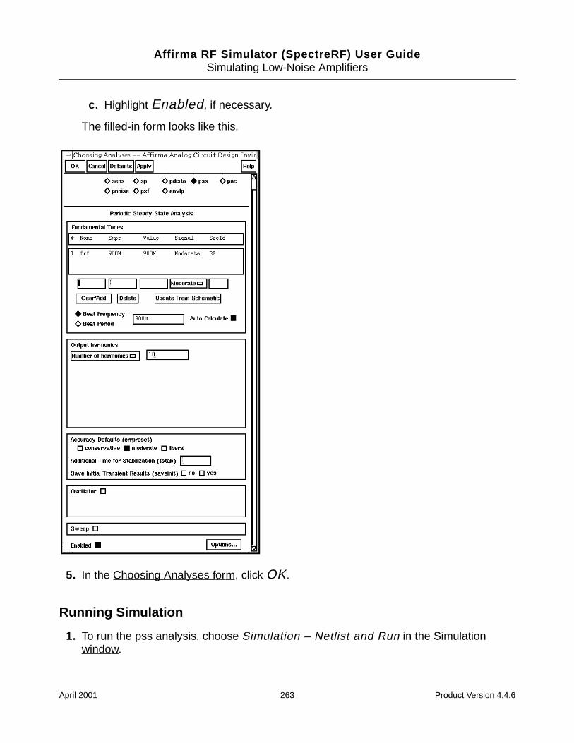
Affirma RF Simulator (SpectreRF) User GuideSimulating Low-Noise Amplifiers
c. Highlight Enabled, if necessary.
The filled-in form looks like this.
5. In the Choosing Analyses form, click OK.
Running Simulation
1. To run the pss analysis, choose Simulation – Netlist and Run in the Simulationwindow.
April 2001 263 Product Version 4.4.6
Affirma RF Simulator (SpectreRF) User GuideSimulating Low-Noise Amplifiers
The output log file appears and displays information about the simulation as it runs.
2. Look in the output log file to be sure the simulation is completed successfully.
Plotting Voltage Gain
In the Simulation window, choose Results – Direct Plot – PSS.
The Waveform window and the PSS Results form appear.
In the PSS Results form, do the following:
1. Highlight Replace for Plot Mode.
2. Highlight pss for Analysis Type.
3. Highlight Voltage Gain for Function.
4. Highlight dB20 for Modifier.
5. Highlight 900M in the Reference Harmonic window.
April 2001 264 Product Version 4.4.6
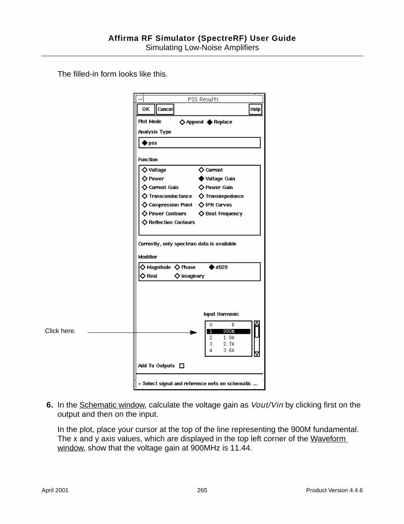
Affirma RF Simulator (SpectreRF) User GuideSimulating Low-Noise Amplifiers
The filled-in form looks like this.
6. In the Schematic window, calculate the voltage gain as Vout/Vin by clicking first on theoutput and then on the input.
In the plot, place your cursor at the top of the line representing the 900M fundamental.The x and y axis values, which are displayed in the top left corner of the Waveformwindow, show that the voltage gain at 900MHz is 11.44.
Click here.
April 2001 265 Product Version 4.4.6
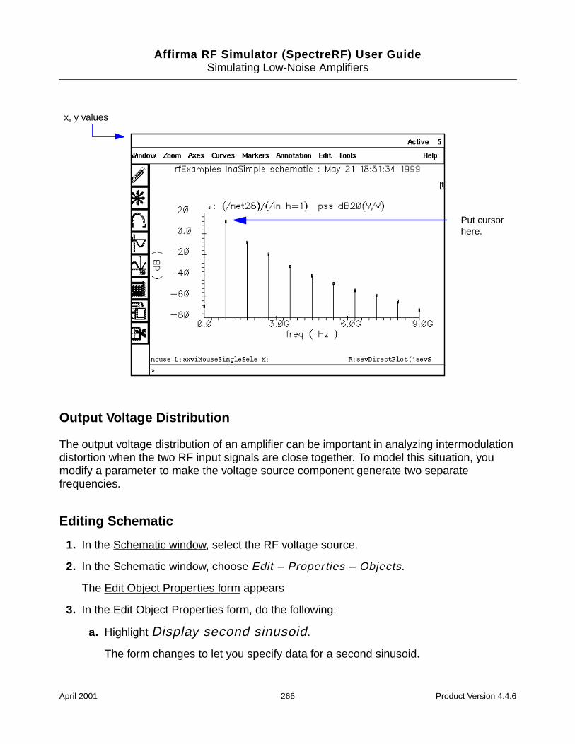
Affirma RF Simulator (SpectreRF) User GuideSimulating Low-Noise Amplifiers
Output Voltage Distribution
The output voltage distribution of an amplifier can be important in analyzing intermodulationdistortion when the two RF input signals are close together. To model this situation, youmodify a parameter to make the voltage source component generate two separatefrequencies.
Editing Schematic
1. In the Schematic window, select the RF voltage source.
2. In the Schematic window, choose Edit – Properties – Objects.
The Edit Object Properties form appears
3. In the Edit Object Properties form, do the following:
a. Highlight Display second sinusoid.
The form changes to let you specify data for a second sinusoid.
Put cursorhere.
x, y values
April 2001 266 Product Version 4.4.6
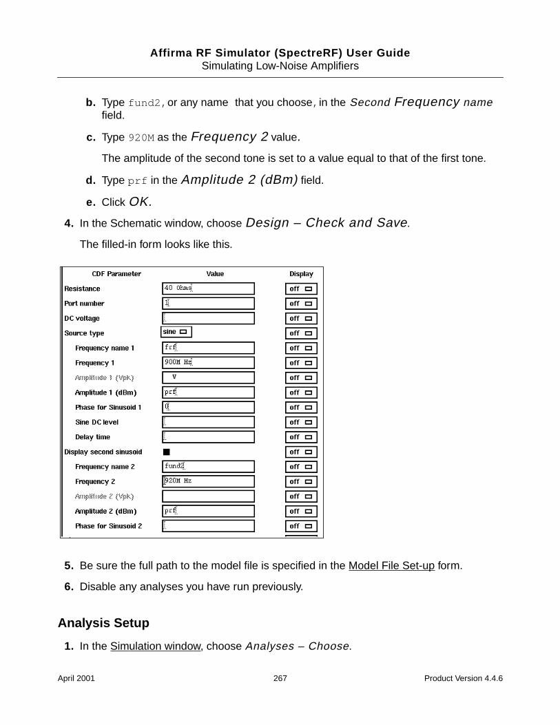
Affirma RF Simulator (SpectreRF) User GuideSimulating Low-Noise Amplifiers
b. Type fund2, or any name that you choose, in the Second Frequency namefield.
c. Type 920M as the Frequency 2 value.
The amplitude of the second tone is set to a value equal to that of the first tone.
d. Type prf in the Amplitude 2 (dBm) field.
e. Click OK.
4. In the Schematic window, choose Design – Check and Save.
The filled-in form looks like this.
5. Be sure the full path to the model file is specified in the Model File Set-up form.
6. Disable any analyses you have run previously.
Analysis Setup
1. In the Simulation window, choose Analyses – Choose.
April 2001 267 Product Version 4.4.6

Affirma RF Simulator (SpectreRF) User GuideSimulating Low-Noise Amplifiers
The Choosing Analyses form appears.
2. Click on pss for the Analysis choice.
3. In the Fundamental Tones list box, be sure the Auto Calculate button ishighlighted.
The Beat Frequency field shows 20Mbecause there are two RF tones at 900M and920M.
The Beat Frequency button is highlighted by default.
In the Choosing Analyses form, do the following:
1. In the Output harmonics cyclic field, choose Number of Harmonics and type60 in the Number of Harmonics field.
The largest common multiple of 900Mhz and 920Mhz is 20Mhz. Sixty harmonics extendsthe results out to 1.2 GHz, but you can choose another number if you want.
2. Highlight moderate as the Accuracy Defaults value
April 2001 268 Product Version 4.4.6
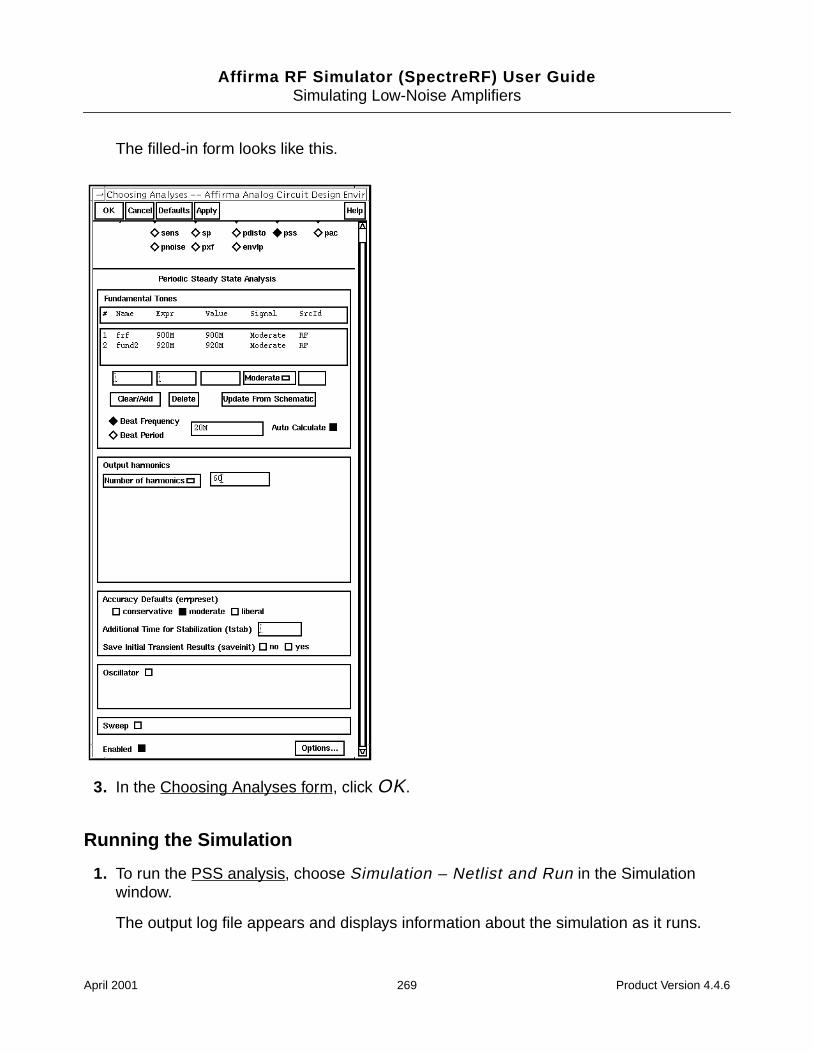
Affirma RF Simulator (SpectreRF) User GuideSimulating Low-Noise Amplifiers
The filled-in form looks like this.
3. In the Choosing Analyses form, click OK.
Running the Simulation
1. To run the PSS analysis, choose Simulation – Netlist and Run in the Simulationwindow.
The output log file appears and displays information about the simulation as it runs.
April 2001 269 Product Version 4.4.6
Affirma RF Simulator (SpectreRF) User GuideSimulating Low-Noise Amplifiers
2. Look in the CIW for a message that says the simulation completed successfully.
Plotting Output Voltage Distribution
In the Simulation window, choose Results – Direct Plot – PSS.
The Waveform window and the PSS Results form appear.
In the PSS Results form, do the following:
1. Highlight Replace for Plot Mode.
2. Highlight Voltage for Function.
3. Highlight spectrum for Sweep value.
4. Highlight dB20 for Modifier.
April 2001 270 Product Version 4.4.6
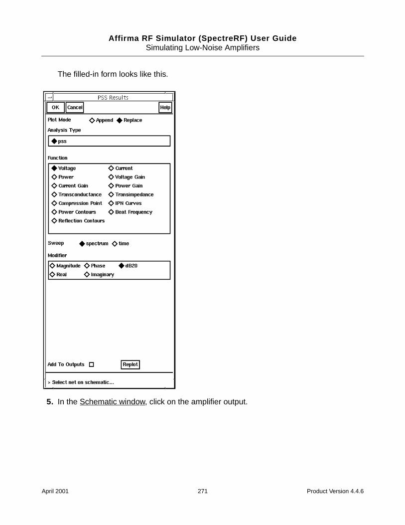
Affirma RF Simulator (SpectreRF) User GuideSimulating Low-Noise Amplifiers
The filled-in form looks like this.
5. In the Schematic window, click on the amplifier output.
April 2001 271 Product Version 4.4.6
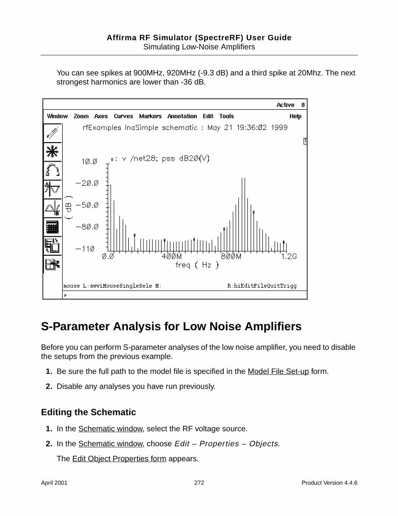
Affirma RF Simulator (SpectreRF) User GuideSimulating Low-Noise Amplifiers
You can see spikes at 900MHz, 920MHz (-9.3 dB) and a third spike at 20Mhz. The nextstrongest harmonics are lower than -36 dB.
S-Parameter Analysis for Low Noise Amplifiers
Before you can perform S-parameter analyses of the low noise amplifier, you need to disablethe setups from the previous example.
1. Be sure the full path to the model file is specified in the Model File Set-up form.
2. Disable any analyses you have run previously.
Editing the Schematic
1. In the Schematic window, select the RF voltage source.
2. In the Schematic window, choose Edit – Properties – Objects.
The Edit Object Properties form appears.
April 2001 272 Product Version 4.4.6
Affirma RF Simulator (SpectreRF) User GuideSimulating Low-Noise Amplifiers
3. In the Edit Object Properties form, be sure the Source type is set to sine , delete theFrequency 2 value, if there is one, and click OK.
The input voltage source now has only one frequency at 900MHz. Frequency2 iszero.
4. In the Schematic window, choose Design – Check and Save.
Analysis Setup
1. In the Simulation window, choose Analyses – Choose.
The Choosing Analyses form appears.
2. In the Choosing Analyses form, click on sp for the Analysis choice.
The form changes to let you specify data for an S-parameter analysis.
3. In the Choosing Analyses form, do the following:
a. Highlight Frequency for Sweep Variable.
b. Highlight Start-Stop for Sweep Range and type 100M and 1.2G as theStart and Stop values, respectively.
c. In the Sweep Type cyclic field, choose Linear and click on theNumber of Steps button.
d. Type 100 for the Number of Steps in the field.
April 2001 273 Product Version 4.4.6
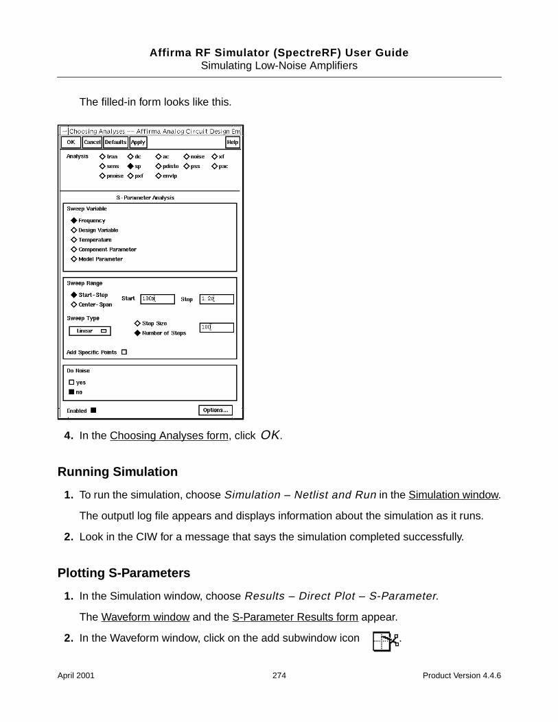
Affirma RF Simulator (SpectreRF) User GuideSimulating Low-Noise Amplifiers
The filled-in form looks like this.
4. In the Choosing Analyses form, click OK.
Running Simulation
1. To run the simulation, choose Simulation – Netlist and Run in the Simulation window.
The outputl log file appears and displays information about the simulation as it runs.
2. Look in the CIW for a message that says the simulation completed successfully.
Plotting S-Parameters
1. In the Simulation window, choose Results – Direct Plot – S-Parameter.
The Waveform window and the S-Parameter Results form appear.
2. In the Waveform window, click on the add subwindow icon .
April 2001 274 Product Version 4.4.6
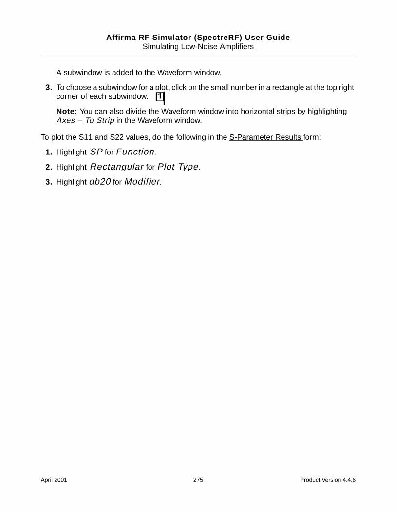
Affirma RF Simulator (SpectreRF) User GuideSimulating Low-Noise Amplifiers
A subwindow is added to the Waveform window,
3. To choose a subwindow for a plot, click on the small number in a rectangle at the top rightcorner of each subwindow.
Note: You can also divide the Waveform window into horizontal strips by highlightingAxes – To Strip in the Waveform window.
To plot the S11 and S22 values, do the following in the S-Parameter Results form:
1. Highlight SP for Function.
2. Highlight Rectangular for Plot Type.
3. Highlight db20 for Modifier.
April 2001 275 Product Version 4.4.6
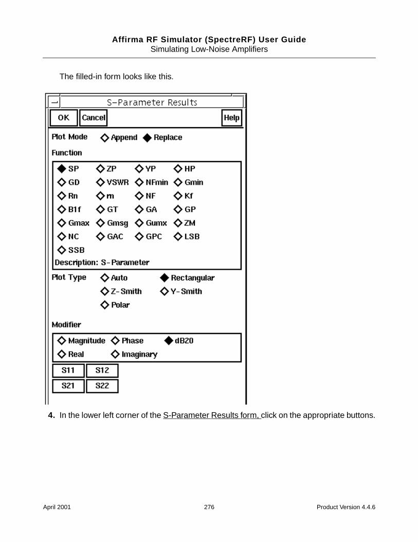
Affirma RF Simulator (SpectreRF) User GuideSimulating Low-Noise Amplifiers
The filled-in form looks like this.
4. In the lower left corner of the S-Parameter Results form, click on the appropriate buttons.
April 2001 276 Product Version 4.4.6
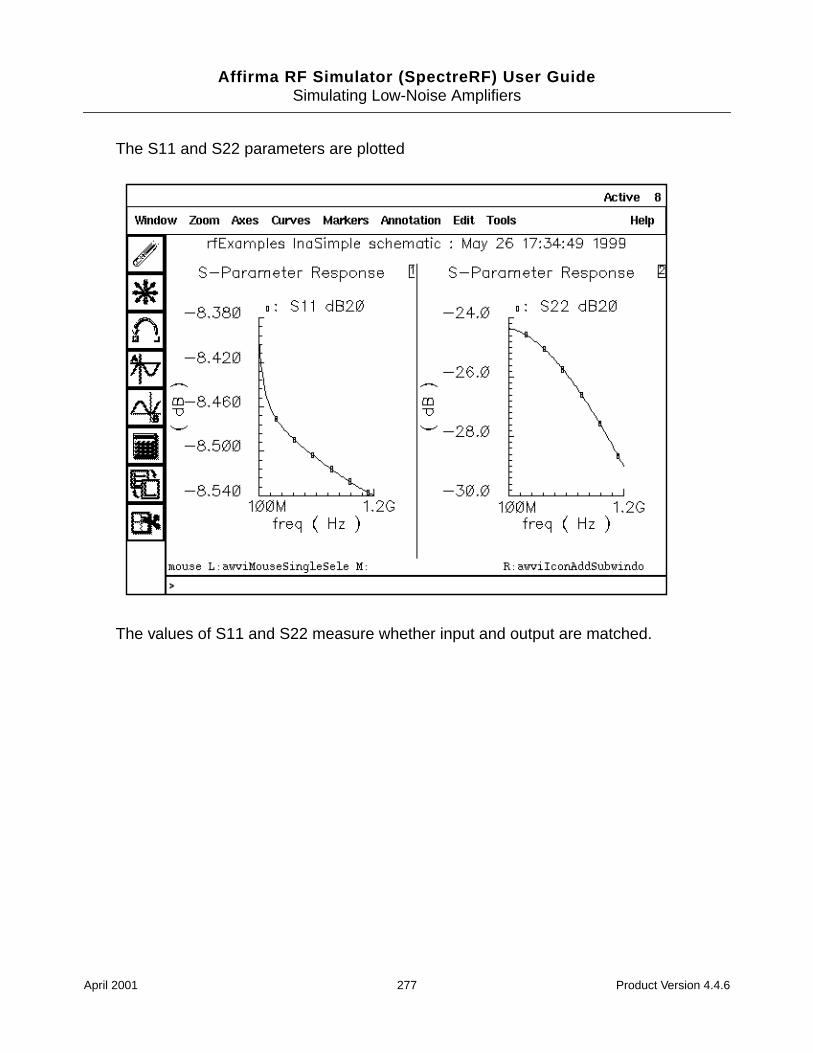
Affirma RF Simulator (SpectreRF) User GuideSimulating Low-Noise Amplifiers
The S11 and S22 parameters are plotted
The values of S11 and S22 measure whether input and output are matched.
April 2001 277 Product Version 4.4.6
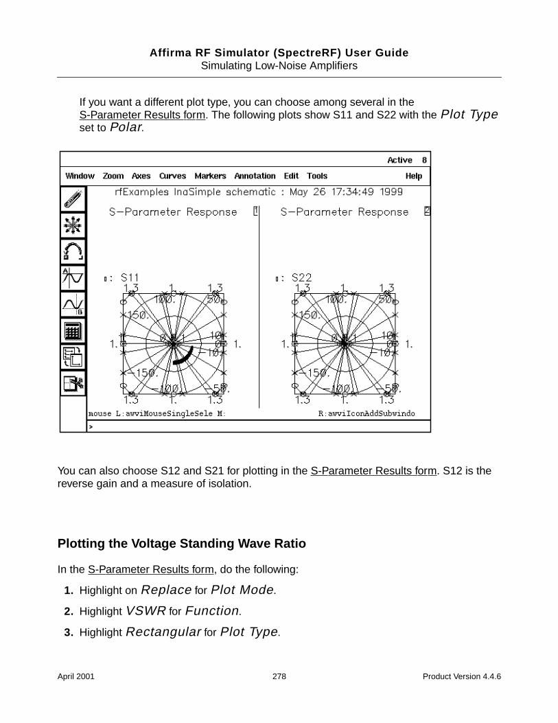
Affirma RF Simulator (SpectreRF) User GuideSimulating Low-Noise Amplifiers
If you want a different plot type, you can choose among several in theS-Parameter Results form. The following plots show S11 and S22 with the Plot Typeset to Polar.
You can also choose S12 and S21 for plotting in the S-Parameter Results form. S12 is thereverse gain and a measure of isolation.
Plotting the Voltage Standing Wave Ratio
In the S-Parameter Results form, do the following:
1. Highlight on Replace for Plot Mode.
2. Highlight VSWR for Function.
3. Highlight Rectangular for Plot Type.
April 2001 278 Product Version 4.4.6
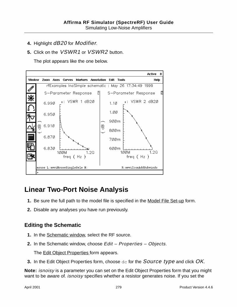
Affirma RF Simulator (SpectreRF) User GuideSimulating Low-Noise Amplifiers
4. Highlight dB20 for Modifier.
5. Click on the VSWR1 or VSWR2 button.
The plot appears like the one below.
Linear Two-Port Noise Analysis
1. Be sure the full path to the model file is specified in the Model File Set-up form.
2. Disable any analyses you have run previously.
Editing the Schematic
1. In the Schematic window, select the RF source.
2. In the Schematic window, choose Edit – Properties – Objects.
The Edit Object Properties form appears.
3. In the Edit Object Properties form, choose dc for the Source type and click OK.
Note: isnoisy is a parameter you can set on the Edit Object Properties form that you mightwant to be aware of. isnoisy specifies whether a resistor generates noise. If you set the
April 2001 279 Product Version 4.4.6
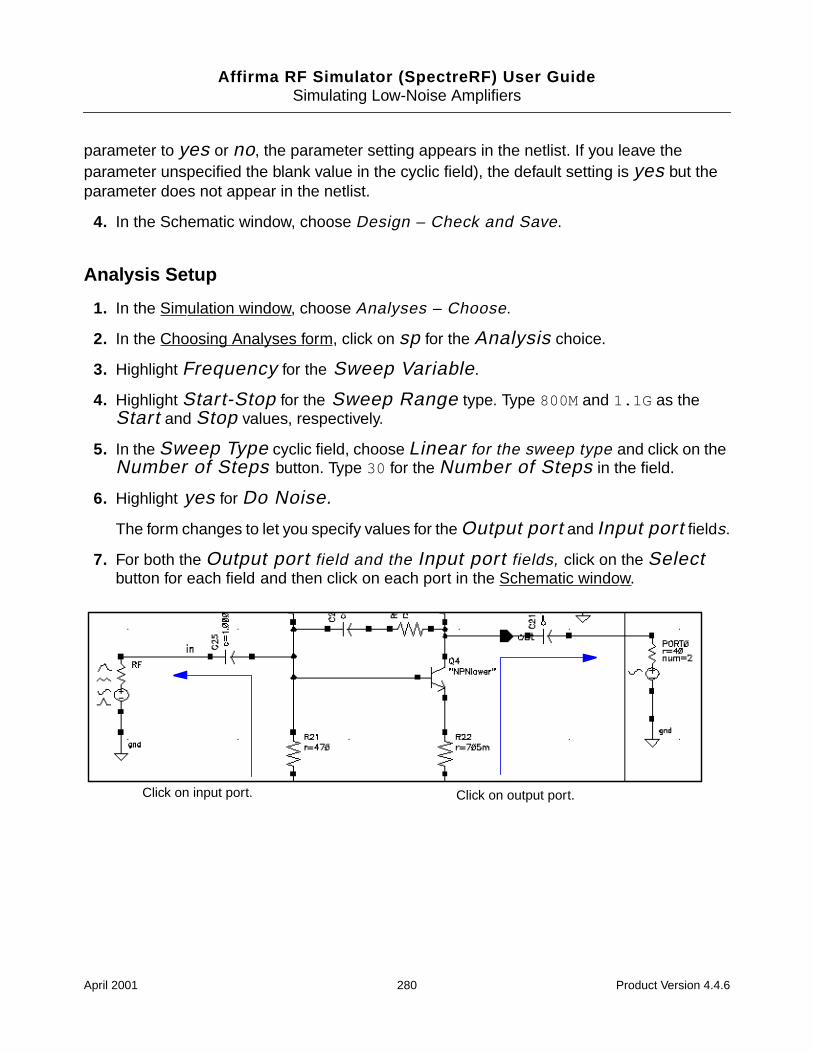
Affirma RF Simulator (SpectreRF) User GuideSimulating Low-Noise Amplifiers
parameter to yes or no, the parameter setting appears in the netlist. If you leave theparameter unspecified the blank value in the cyclic field), the default setting is yes but theparameter does not appear in the netlist.
4. In the Schematic window, choose Design – Check and Save.
Analysis Setup
1. In the Simulation window, choose Analyses – Choose.
2. In the Choosing Analyses form, click on sp for the Analysis choice.
3. Highlight Frequency for the Sweep Variable.
4. Highlight Start-Stop for the Sweep Range type. Type 800M and 1.1G as theStart and Stop values, respectively.
5. In the Sweep Type cyclic field, choose Linear for the sweep type and click on theNumber of Steps button. Type 30 for the Number of Steps in the field.
6. Highlight yes for Do Noise.
The form changes to let you specify values for the Output port and Input port fields.
7. For both the Output port field and the Input port fields, click on the Selectbutton for each field and then click on each port in the Schematic window.
Click on input port. Click on output port.
April 2001 280 Product Version 4.4.6
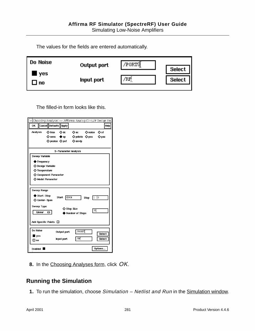
Affirma RF Simulator (SpectreRF) User GuideSimulating Low-Noise Amplifiers
The values for the fields are entered automatically.
The filled-in form looks like this.
8. In the Choosing Analyses form, click OK.
Running the Simulation
1. To run the simulation, choose Simulation – Netlist and Run in the Simulation window.
April 2001 281 Product Version 4.4.6
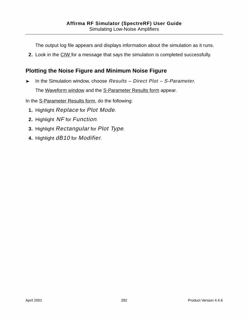
Affirma RF Simulator (SpectreRF) User GuideSimulating Low-Noise Amplifiers
The output log file appears and displays information about the simulation as it runs.
2. Look in the CIW for a message that says the simulation is completed successfully.
Plotting the Noise Figure and Minimum Noise Figure
In the Simulation window, choose Results – Direct Plot – S-Parameter.
The Waveform window and the S-Parameter Results form appear.
In the S-Parameter Results form, do the following:
1. Highlight Replace for Plot Mode.
2. Highlight NF for Function.
3. Highlight Rectangular for Plot Type.
4. Highlight dB10 for Modifier.
April 2001 282 Product Version 4.4.6
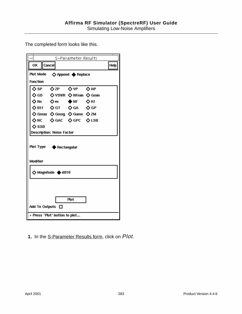
Affirma RF Simulator (SpectreRF) User GuideSimulating Low-Noise Amplifiers
The completed form looks like this.
1. In the S-Parameter Results form, click on Plot.
April 2001 283 Product Version 4.4.6
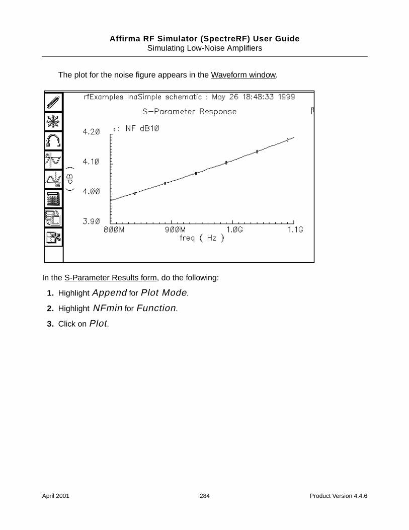
Affirma RF Simulator (SpectreRF) User GuideSimulating Low-Noise Amplifiers
The plot for the noise figure appears in the Waveform window.
In the S-Parameter Results form, do the following:
1. Highlight Append for Plot Mode.
2. Highlight NFmin for Function.
3. Click on Plot.
April 2001 284 Product Version 4.4.6
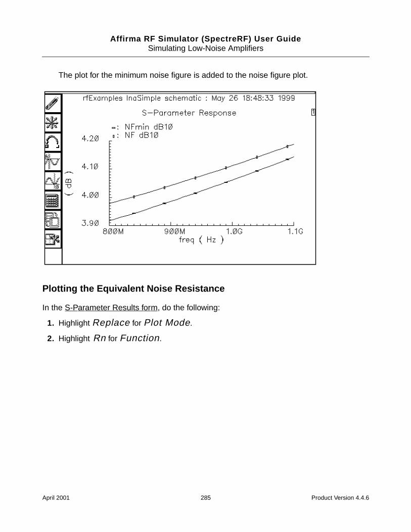
Affirma RF Simulator (SpectreRF) User GuideSimulating Low-Noise Amplifiers
The plot for the minimum noise figure is added to the noise figure plot.
Plotting the Equivalent Noise Resistance
In the S-Parameter Results form, do the following:
1. Highlight Replace for Plot Mode.
2. Highlight Rn for Function.
April 2001 285 Product Version 4.4.6
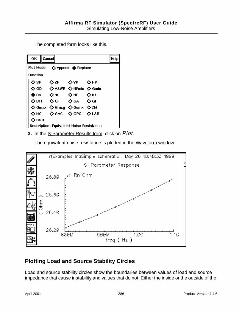
Affirma RF Simulator (SpectreRF) User GuideSimulating Low-Noise Amplifiers
The completed form looks like this.
3. In the S-Parameter Results form, click on Plot.
The equivalent noise resistance is plotted in the Waveform window.
Plotting Load and Source Stability Circles
Load and source stability circles show the boundaries between values of load and sourceimpedance that cause instability and values that do not. Either the inside or the outside of the
April 2001 286 Product Version 4.4.6
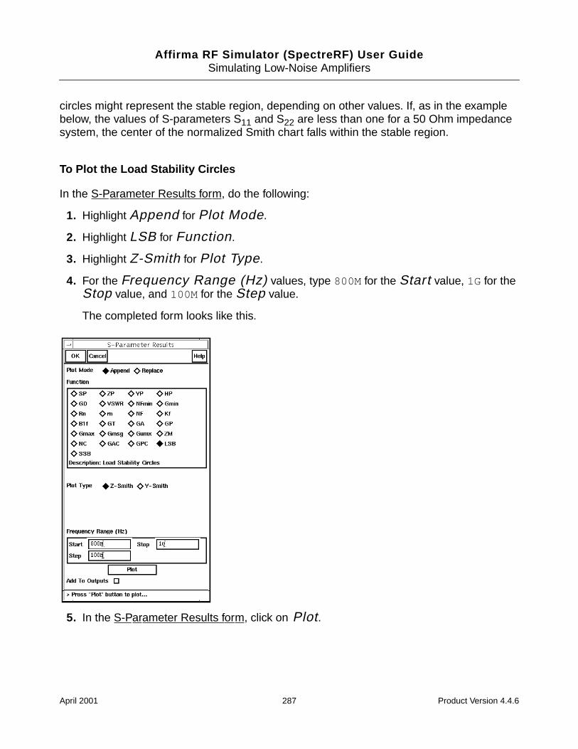
Affirma RF Simulator (SpectreRF) User GuideSimulating Low-Noise Amplifiers
circles might represent the stable region, depending on other values. If, as in the examplebelow, the values of S-parameters S11 and S22 are less than one for a 50 Ohm impedancesystem, the center of the normalized Smith chart falls within the stable region.
To Plot the Load Stability Circles
In the S-Parameter Results form, do the following:
1. Highlight Append for Plot Mode.
2. Highlight LSB for Function.
3. Highlight Z-Smith for Plot Type.
4. For the Frequency Range (Hz) values, type 800M for the Start value, 1G for theStop value, and 100M for the Step value.
The completed form looks like this.
5. In the S-Parameter Results form, click on Plot.
April 2001 287 Product Version 4.4.6
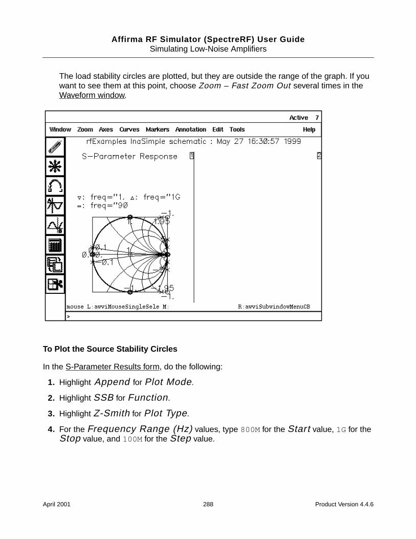
Affirma RF Simulator (SpectreRF) User GuideSimulating Low-Noise Amplifiers
The load stability circles are plotted, but they are outside the range of the graph. If youwant to see them at this point, choose Zoom – Fast Zoom Out several times in theWaveform window.
To Plot the Source Stability Circles
In the S-Parameter Results form, do the following:
1. Highlight Append for Plot Mode.
2. Highlight SSB for Function.
3. Highlight Z-Smith for Plot Type.
4. For the Frequency Range (Hz) values, type 800M for the Start value, 1G for theStop value, and 100M for the Step value.
April 2001 288 Product Version 4.4.6
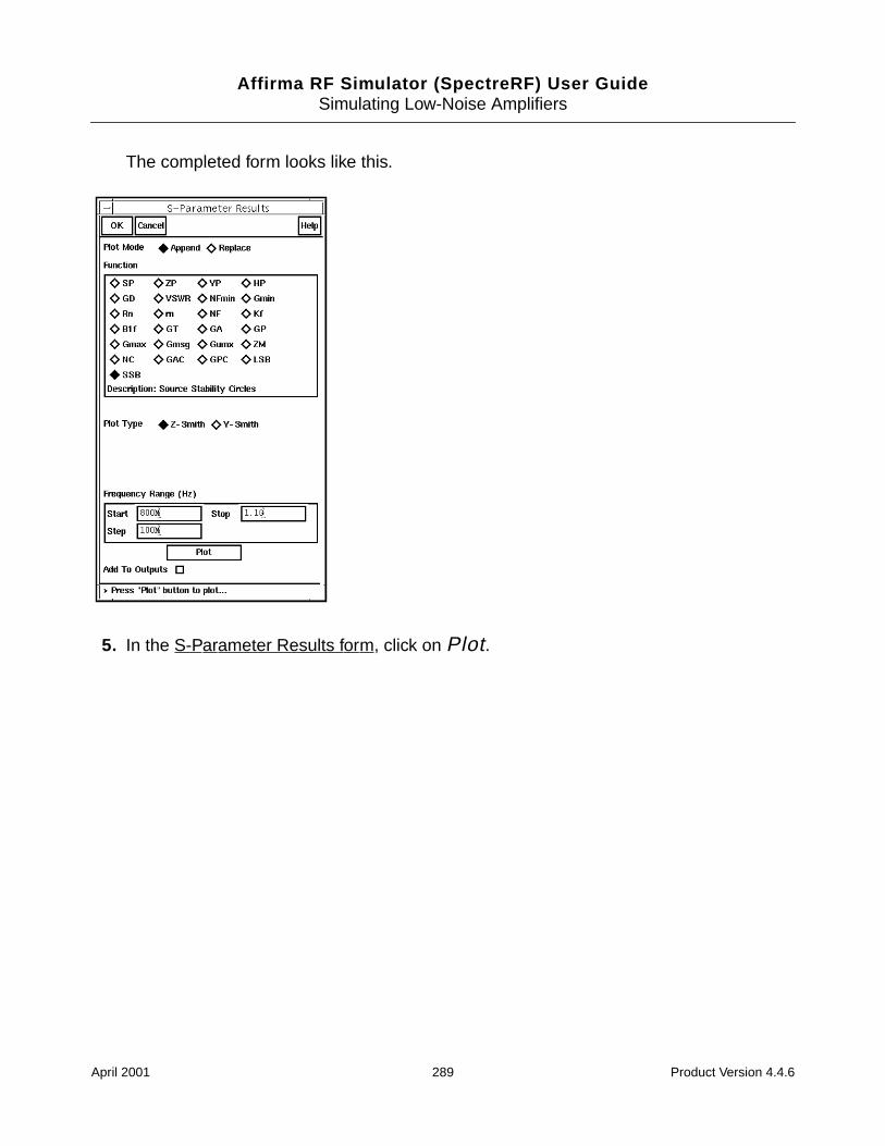
Affirma RF Simulator (SpectreRF) User GuideSimulating Low-Noise Amplifiers
The completed form looks like this.
5. In the S-Parameter Results form, click on Plot.
April 2001 289 Product Version 4.4.6
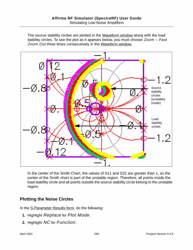
Affirma RF Simulator (SpectreRF) User GuideSimulating Low-Noise Amplifiers
The source stability circles are plotted in the Waveform window along with the loadstability circles. To see the plot as it appears below, you must choose Zoom – FastZoom Out three times consecutively in the Waveform window.
In the center of the Smith Chart, the values of S11 and S22 are greater than 1, so thecenter of the Smith chart is part of the unstable region. Therefore, all points inside theload stability circle and all points outside the source stability circle belong to the unstableregion.
Plotting the Noise Circles
In the S-Parameter Results form, do the following:
1. Highlight Replace for Plot Mode.
2. Highlight NC for Function.
Sourcestabilitycircles(unstable)Inside)
Loadstabilitycircles
April 2001 290 Product Version 4.4.6
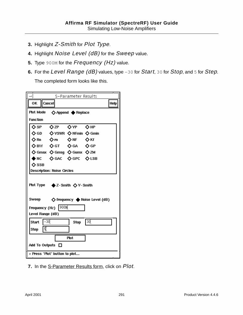
Affirma RF Simulator (SpectreRF) User GuideSimulating Low-Noise Amplifiers
3. Highlight Z-Smith for Plot Type.
4. Highlight Noise Level (dB) for the Sweep value.
5. Type 900M for the Frequency (Hz) value.
6. For the Level Range (dB) values, type -30 for Start, 30 for Stop, and 5 for Step.
The completed form looks like this.
7. In the S-Parameter Results form, click on Plot.
April 2001 291 Product Version 4.4.6
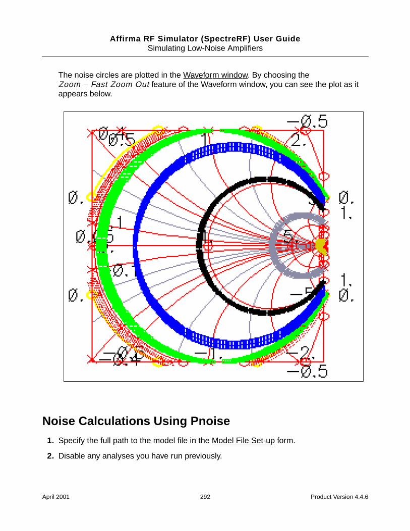
Affirma RF Simulator (SpectreRF) User GuideSimulating Low-Noise Amplifiers
The noise circles are plotted in the Waveform window. By choosing theZoom – Fast Zoom Out feature of the Waveform window, you can see the plot as itappears below.
Noise Calculations Using Pnoise
1. Specify the full path to the model file in the Model File Set-up form.
2. Disable any analyses you have run previously.
April 2001 292 Product Version 4.4.6

Affirma RF Simulator (SpectreRF) User GuideSimulating Low-Noise Amplifiers
Editing the Schematic
1. In the Schematic window, choose Edit – Properties – Objects.
2. In the Schematic window, click on the RFvoltage source.
The Edit Object Properties form appears.
3. In the Edit Object Properties form, choose dc for the Source Type and then click OK.
4. In the Schematic window, choose Design – Check and Save.
Analysis Setup
1. In the Simulation window, choose Analyses – Choose.
The Choosing Analyses form appears.
2. In the Choosing Analyses form, click on pss.
3. Type 900M for the Beat Frequency.
With the dc source type, you must enter the fundamental frequency manually.
Be sure the Auto Calculate button is not highlighted.
4. The Beat Frequency button is highlighted by default.
5. In the Output harmonics cyclic field, choose Number of harmonics for theOutput harmonics choice, and type in a reasonable value, such as 20, for thenumber of harmonics.
6. Highlight conservative for the Accuracy Defaults (errpreset) value.
April 2001 293 Product Version 4.4.6
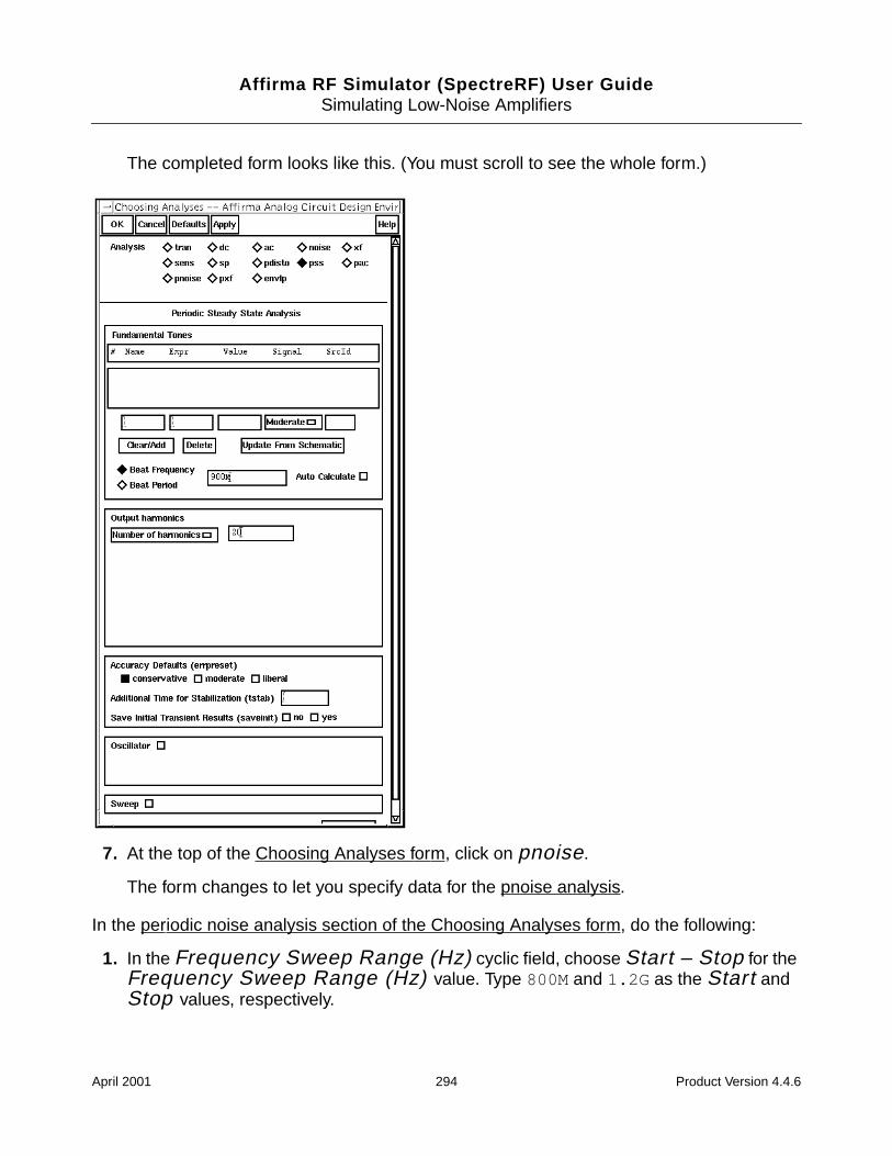
Affirma RF Simulator (SpectreRF) User GuideSimulating Low-Noise Amplifiers
The completed form looks like this. (You must scroll to see the whole form.)
7. At the top of the Choosing Analyses form, click on pnoise.
The form changes to let you specify data for the pnoise analysis.
In the periodic noise analysis section of the Choosing Analyses form, do the following:
1. In the Frequency Sweep Range (Hz) cyclic field, choose Start – Stop for theFrequency Sweep Range (Hz) value. Type 800M and 1.2G as the Start andStop values, respectively.
April 2001 294 Product Version 4.4.6
Affirma RF Simulator (SpectreRF) User GuideSimulating Low-Noise Amplifiers
2. In the Sweep Type cyclic field, choose Linear for the sweep type and click on theNumber of Steps button. Type 201 as the number of steps.
3. In the Sidebands cyclic field choose Maximum sideband and type 20 for theMaximum sideband value in the field.
4. Choose voltage for the Output.
The value is appropriate because the reference sideband is an LNA.
5. Click on the Positive Output Node Select button, and then click in the schematicto choose the amplifier output.
6. Leave the Negative Output Node field empty. It defaults to /gnd!
You can set the Negative Output Node to a different value by clicking on theNegative Output Node Select button and then clicking on the output node in theschematic.
7. In the Input Voltage Source cyclic field, choose voltage.
8. Click on the Input Source Select button, and then click in the schematic on the RFvoltage source.
9. Type 0 for the Reference Side-Band value.
The reference sideband is specified as 0 because the circuit is an LNA, and there is nofrequency conversion from the input to the output.
April 2001 295 Product Version 4.4.6
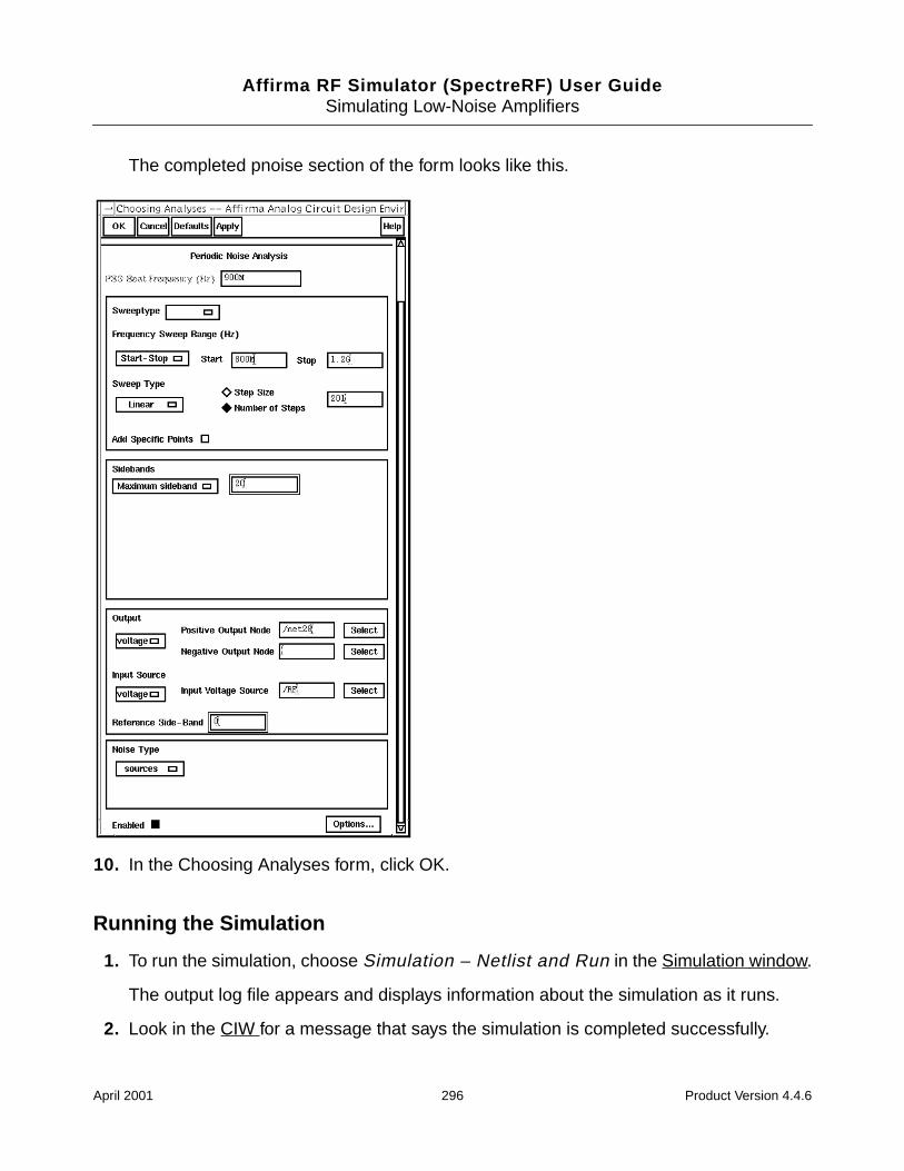
Affirma RF Simulator (SpectreRF) User GuideSimulating Low-Noise Amplifiers
The completed pnoise section of the form looks like this.
10. In the Choosing Analyses form, click OK.
Running the Simulation
1. To run the simulation, choose Simulation – Netlist and Run in the Simulation window.
The output log file appears and displays information about the simulation as it runs.
2. Look in the CIW for a message that says the simulation is completed successfully.
April 2001 296 Product Version 4.4.6
Affirma RF Simulator (SpectreRF) User GuideSimulating Low-Noise Amplifiers
Plotting the Noise Calculations
In the Simulation window, choose Results – Direct Plot – PSS.
The Waveform window and the PSS Results form appear.
In the PSS Results form, do the following:
1. Highlight Replace for Plot Mode.
2. Highlight pnoise for Analysis Type.
3. Highlight Noise Figure for Function.
April 2001 297 Product Version 4.4.6
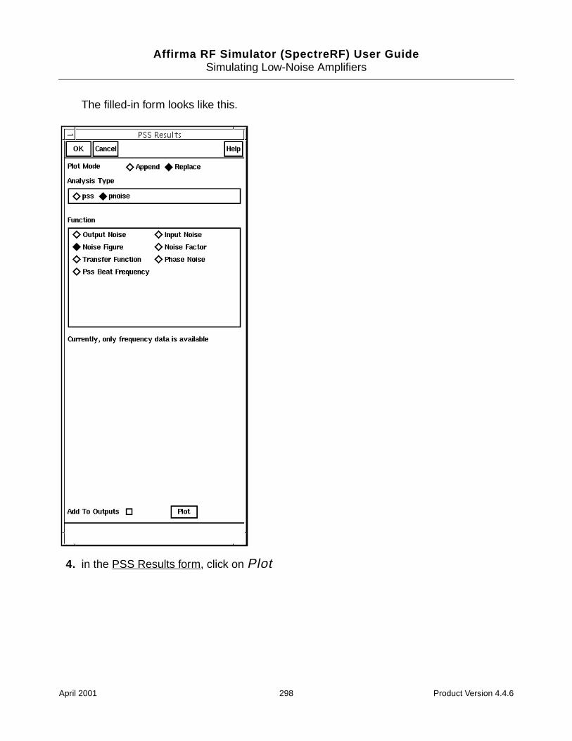
Affirma RF Simulator (SpectreRF) User GuideSimulating Low-Noise Amplifiers
The filled-in form looks like this.
4. in the PSS Results form, click on Plot
April 2001 298 Product Version 4.4.6
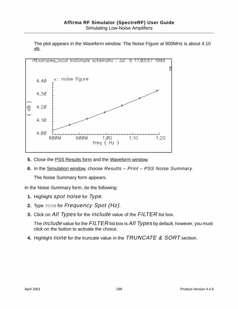
Affirma RF Simulator (SpectreRF) User GuideSimulating Low-Noise Amplifiers
The plot appears in the Waveform window. The Noise Figure at 900MHz is about 4.10dB.
5. Close the PSS Results form and the Waveform window.
6. In the Simulation window, choose Results – Print – PSS Noise Summary.
The Noise Summary form appears.
In the Noise Summary form, do the following:
1. Highlight spot noise for Type.
2. Type 900M for Frequency Spot (Hz).
3. Click on All Types for the include value of the FILTER list box.
The include value for the FILTER list box is All Types by default, however, you mustclick on the button to activate the choice.
4. Highlight none for the truncate value in the TRUNCATE & SORT section.
April 2001 299 Product Version 4.4.6
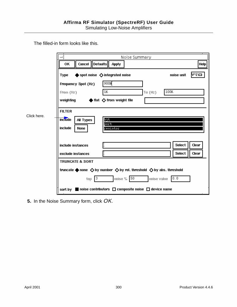
Affirma RF Simulator (SpectreRF) User GuideSimulating Low-Noise Amplifiers
The filled-in form looks like this.
5. In the Noise Summary form, click OK.
Click here.
April 2001 300 Product Version 4.4.6
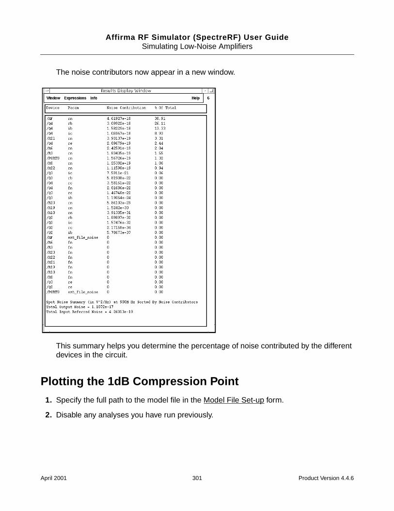
Affirma RF Simulator (SpectreRF) User GuideSimulating Low-Noise Amplifiers
The noise contributors now appear in a new window.
This summary helps you determine the percentage of noise contributed by the differentdevices in the circuit.
Plotting the 1dB Compression Point
1. Specify the full path to the model file in the Model File Set-up form.
2. Disable any analyses you have run previously.
April 2001 301 Product Version 4.4.6
Affirma RF Simulator (SpectreRF) User GuideSimulating Low-Noise Amplifiers
Editing the Schematic
Click on the input voltage source (instance RF) and then choose Edit – Properties –Objects in the Schematic window.
The Edit Object Properties form appears.
In the Edit Object Properties form, do the following:
1. Choose sine for the Source Type.
2. Type 900M for the Frequency value.
3. Type prf for the Amplitude (dBm) value.
4. Be sure the Amplitude field is empty.
5. In the Edit Objects Properties form, click OK.
6. In the Schematic window, choose Design – Check and Save.
Analysis Setup
1. In the Simulation window, choose Analyses – Choose.
The Choosing Analyses form appears.
2. In the Choosing Analyses form, click on pss.
In the Choosing Analyses form, do the following:
1. Type 100M for the Fundamental Frequency.
The Beat Frequency button is highlighted by default.
Be sure the Auto Calculate button is not highlighted.
2. In the Output harmonics cyclic field, choose Number of harmonics for theOutput harmonics choice and type in a reasonable value, such as 10 , in the numberof harmonics field.
3. Highlight moderate for the Accuracy Default (errpreset).
4. Highlight the Sweep button.
The form changes to let you specify data for the sweep.
5. In the Sweep cyclic field, choose Variable.
6. Click on the Select Design Variable button.
April 2001 302 Product Version 4.4.6

Affirma RF Simulator (SpectreRF) User GuideSimulating Low-Noise Amplifiers
The Select Design Variable form appears.
7. In the Select Design variable form, highlight prf and click OK.
prf is the amplitude, in dBm, of the RF input source. If you are not sure of this, use theEdit Object Properties form to examine theAmplitude (dBm) field for the RF voltage source.
8. Choose Start-Stop for the Sweep range and type -30 and 10 as the Startand Stop values, respectively, in the fields.
9. Choose Linear for the Sweep Type and click on the Number of Steps button.Type 10 as the number of steps in the field.
April 2001 303 Product Version 4.4.6
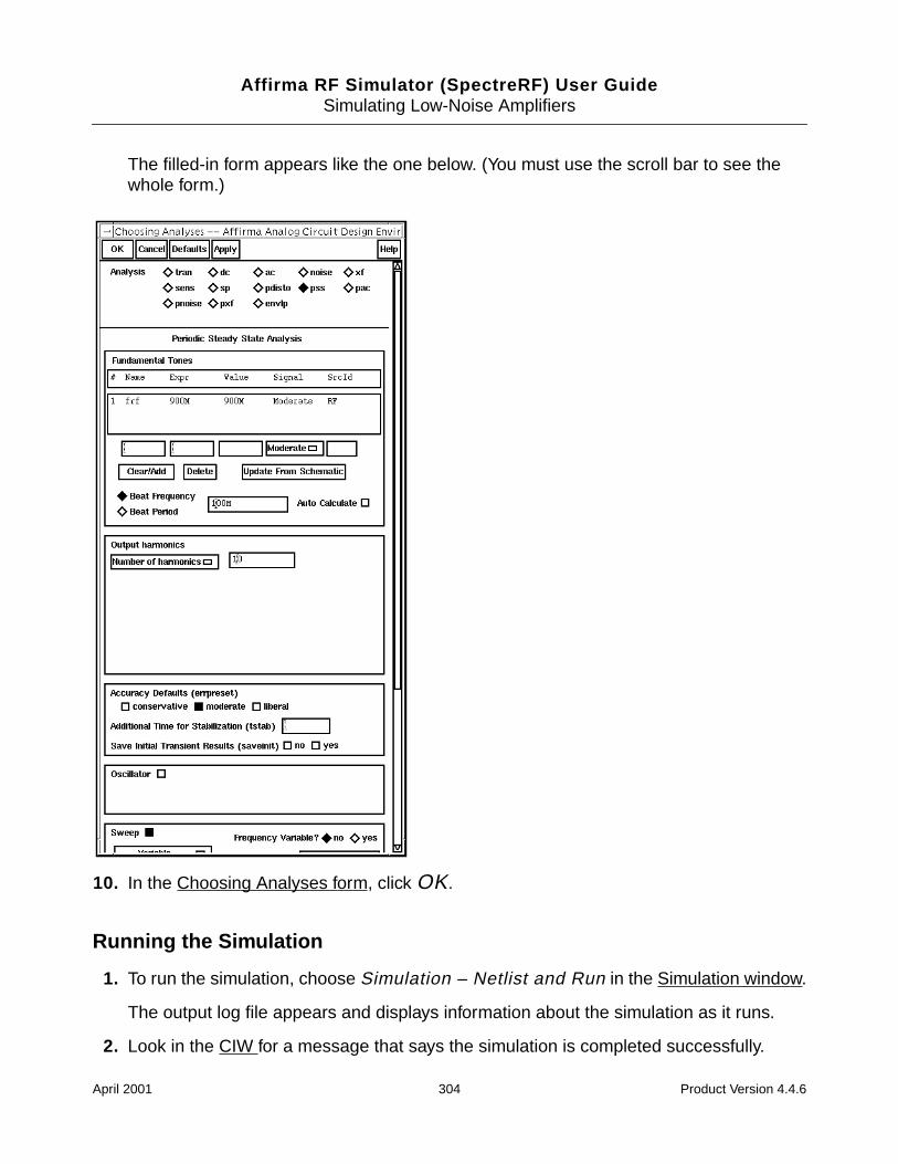
Affirma RF Simulator (SpectreRF) User GuideSimulating Low-Noise Amplifiers
The filled-in form appears like the one below. (You must use the scroll bar to see thewhole form.)
10. In the Choosing Analyses form, click OK.
Running the Simulation
1. To run the simulation, choose Simulation – Netlist and Run in the Simulation window.
The output log file appears and displays information about the simulation as it runs.
2. Look in the CIW for a message that says the simulation is completed successfully.
April 2001 304 Product Version 4.4.6
Affirma RF Simulator (SpectreRF) User GuideSimulating Low-Noise Amplifiers
Plotting the 1dB Compression Point
In the Simulation window, choose Results – Direct Plot – PSS.
The Waveform window and the PSS Results form appear.
In the PSS Results form, do the following:
1. Highlight pss for Analysis Type.
2. Highlight Compression Point for Function.
3. Type -25 for the Extrapolation Point.
You learn what value to use for the extrapolation point through experience. If you do notspecify a value, the plot defaults to the minimum variable value.
4. Choose Input Referred 1dB Compression.
5. Click on 900M in the 1st Order Harmonic list box.
April 2001 305 Product Version 4.4.6
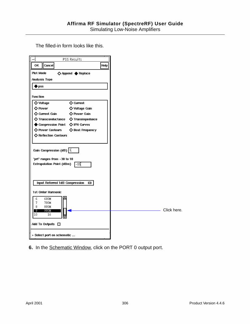
Affirma RF Simulator (SpectreRF) User GuideSimulating Low-Noise Amplifiers
The filled-in form looks like this.
6. In the Schematic Window, click on the PORT 0 output port.
Click here.
April 2001 306 Product Version 4.4.6
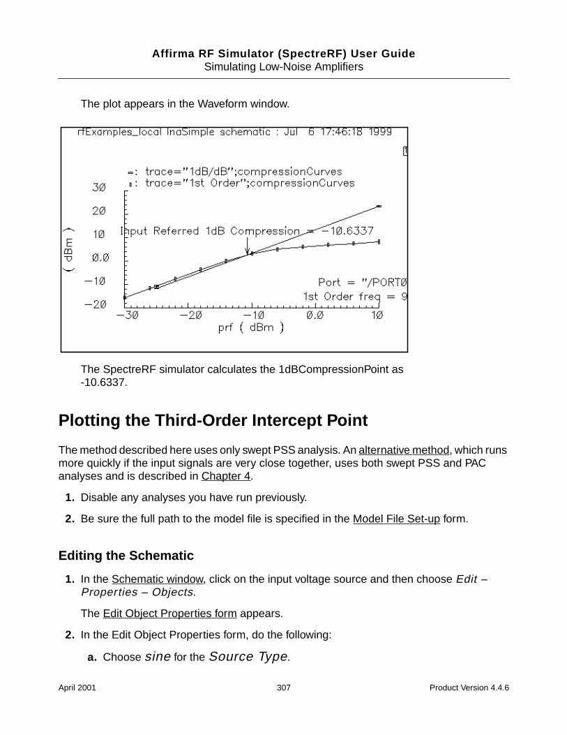
Affirma RF Simulator (SpectreRF) User GuideSimulating Low-Noise Amplifiers
The plot appears in the Waveform window.
The SpectreRF simulator calculates the 1dBCompressionPoint as-10.6337.
Plotting the Third-Order Intercept Point
The method described here uses only swept PSS analysis. An alternative method, which runsmore quickly if the input signals are very close together, uses both swept PSS and PACanalyses and is described in Chapter 4.
1. Disable any analyses you have run previously.
2. Be sure the full path to the model file is specified in the Model File Set-up form.
Editing the Schematic
1. In the Schematic window, click on the input voltage source and then choose Edit –Properties – Objects.
The Edit Object Properties form appears.
2. In the Edit Object Properties form, do the following:
a. Choose sine for the Source Type.
April 2001 307 Product Version 4.4.6
Affirma RF Simulator (SpectreRF) User GuideSimulating Low-Noise Amplifiers
b. Highlight Display second sinusoid.
c. Type fund2 , or any name you choose, in the Second frequency name field.
d. Type prf for the Amplitude (dBm) and Amplitude 2 (dBm) values.
e. Type 900M for the Frequency value.
f. Type 920M for the Frequency 2 value.
g. Be sure the Amplitude and Amplitude2 fields are empty.
3. In the Edit Object Properties form, click OK.
4. In the Schematic window, choose Design – Check and Save.
Analysis Setup
In the Simulation window, choose Analyses – Choose.
The Choosing Analyses form appears.
In the Choosing Analyses form, do the following and then click OK:
1. In the Choosing Analyses form, click on pss.
2. In the Fundamental Tones list box, be sure the Auto calculate button ishighlighted.
The fundamental frequency, 20M, is displayed.
The Beat Frequency button is highlighted by default.
3. In the Output harmonics cyclic field, choose Number of harmonics for theOutput harmonics choice and type in a reasonable value, such as 60 , in the field.
4. Highlight moderate for the Accuracy Defaults (errpreset) value.
5. Highlight the Sweep button.
The form changes to let you specify data for the sweep.
6. In the Sweep cyclic field, choose Variable.
7. Click on the Select Design Variable button.
The Select Design Variable form appears.
8. In the Select Design Variable form, highlight prf and click OK.
April 2001 308 Product Version 4.4.6
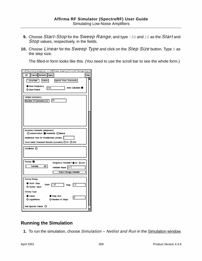
Affirma RF Simulator (SpectreRF) User GuideSimulating Low-Noise Amplifiers
9. Choose Start-Stop for the Sweep Range, and type -30 and 10 as the Start andStop values, respectively, in the fields.
10. Choose Linear for the Sweep Type and click on the Step Size button. Type 5 asthe step size.
The filled-in form looks like this. (You need to use the scroll bar to see the whole form.)
Running the Simulation
1. To run the simulation, choose Simulation – Netlist and Run in the Simulation window.
April 2001 309 Product Version 4.4.6
Affirma RF Simulator (SpectreRF) User GuideSimulating Low-Noise Amplifiers
The output log file appears and displays information about the simulation as it runs.
2. Look in the CIW for a message that says the simulation is completed successfully.
Plotting the Third-Order Intercept Point
In the Simulation window, choose Results – Direct Plot – PSS.
The Waveform window and the PSS Results form appear.
In the PSS Results form, do the following:
1. Highlight Replace for Plot Mode.
2. Highlight pss for Analysis Type.
3. Highlight IPN Curves for Function.
4. Highlight Variable Sweep (“prf ”) for Circuit Input Power.
5. Choose Input Referred IP3.
6. Type -25 for the Extrapolation Point.
You learn what value to use for the extrapolation point through experience. If you do notspecify a value, the plot defaults to the minimum variable value.
7. In the order cyclic field, choose order 3rd.
8. In the 3rd Order Harmonic list box, click on 940M.
9. In the 1st Order Harmonic list box, click on 900M.
Because the two input frequencies are 900MHz and 920MHz, the two-tone, third-orderharmonics are 880MHz and 940MHz. These correspond to the 45th and 47th harmonics.
April 2001 310 Product Version 4.4.6
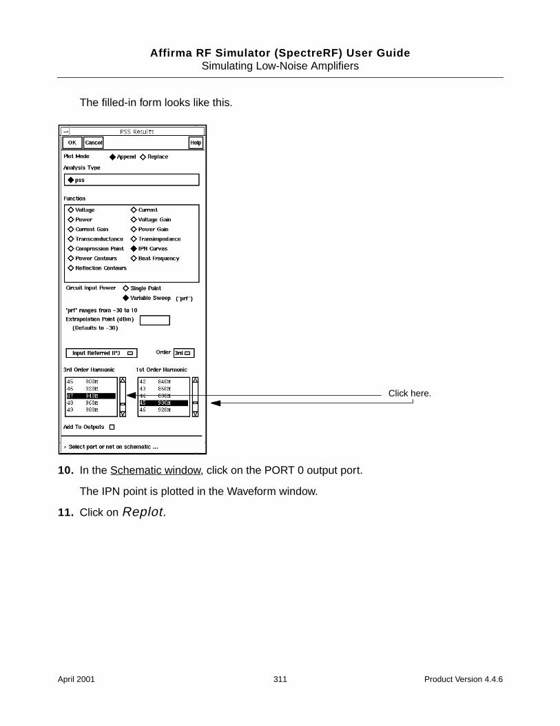
Affirma RF Simulator (SpectreRF) User GuideSimulating Low-Noise Amplifiers
The filled-in form looks like this.
10. In the Schematic window, click on the PORT 0 output port.
The IPN point is plotted in the Waveform window.
11. Click on Replot.
Click here.
April 2001 311 Product Version 4.4.6
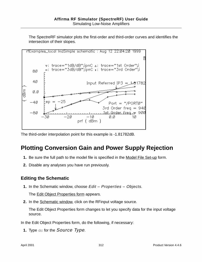
Affirma RF Simulator (SpectreRF) User GuideSimulating Low-Noise Amplifiers
The SpectreRF simulator plots the first-order and third-order curves and identifies theintersection of their slopes.
The third-order interpolation point for this example is -1.81782dB.
Plotting Conversion Gain and Power Supply Rejection
1. Be sure the full path to the model file is specified in the Model File Set-up form.
2. Disable any analyses you have run previously.
Editing the Schematic
1. In the Schematic window, choose Edit – Properties – Objects.
The Edit Object Properties form appears.
2. In the Schematic window, click on the RFinput voltage source.
The Edit Object Properties form changes to let you specify data for the input voltagesource.
In the Edit Object Properties form, do the following, if necessary:
1. Type dc for the Source Type.
April 2001 312 Product Version 4.4.6

Affirma RF Simulator (SpectreRF) User GuideSimulating Low-Noise Amplifiers
2. In the Edit Object Properties form, click OK.
3. To check and save the design, click on the check mark icon in the top left corner of theSchematic window.
Analysis Setup
1. In the Simulation window, choose Analyses – Choose.
The Choosing Analyses form appears.
2. In the Choosing Analyses form, choose pss.
3. Type 900M for the Beat Frequency value.
Because the source type is dc, you must manually enter the fundamental frequency.
The Beat Frequency button is highlighted by default.
Be sure the Auto Calculate button is not highlighted.
4. In the Output harmonics cyclic field, choose Number of harmonics and typein a reasonable value, such as 4, in the field.
5. Highlight conservative for the Accuracy Defaults (errpreset) value.
April 2001 313 Product Version 4.4.6
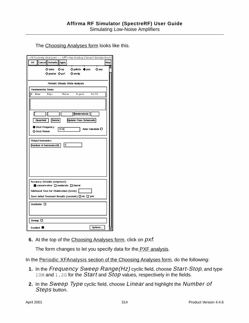
Affirma RF Simulator (SpectreRF) User GuideSimulating Low-Noise Amplifiers
The Choosing Analyses form looks like this.
6. At the top of the Choosing Analyses form, click on pxf.
The form changes to let you specify data for the PXF analysis.
In the Periodic XFAnalysis section of the Choosing Analyses form, do the following:
1. In the Frequency Sweep Range(Hz) cyclic field, choose Start-Stop, and type10M and 1.2G for the Start and Stop values, respectively in the fields.
2. In the Sweep Type cyclic field, choose Linear and highlight the Number ofSteps button.
April 2001 314 Product Version 4.4.6
Affirma RF Simulator (SpectreRF) User GuideSimulating Low-Noise Amplifiers
3. Type 101 for Number of Steps in the field.
4. In the Sidebands cyclic field, choose Maximum sideband for the Sidebandschoice. Type 0 in the field.
5. Choose voltage for the Output choice.
6. Click on the Select button for the Positive Output Node, and then click on theoutput signal in the Schematic window.
7. Highlight the Enabled button for the small-signal analysis, if necessary.
8. Leave the Negative Output Node field empty.
This field defaults to /gnd! You can set the Negative Output Node to a differentvalue by clicking on the Negative Output Node Select button and then clickingon the output node in the schematic.
April 2001 315 Product Version 4.4.6
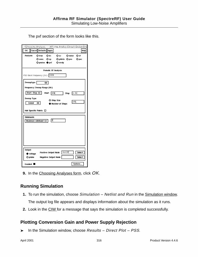
Affirma RF Simulator (SpectreRF) User GuideSimulating Low-Noise Amplifiers
The pxf section of the form looks like this.
9. In the Choosing Analyses form, click OK.
Running Simulation
1. To run the simulation, choose Simulation – Netlist and Run in the Simulation window.
The output log file appears and displays information about the simulation as it runs.
2. Look in the CIW for a message that says the simulation is completed successfully.
Plotting Conversion Gain and Power Supply Rejection
In the Simulation window, choose Results – Direct Plot – PSS.
April 2001 316 Product Version 4.4.6
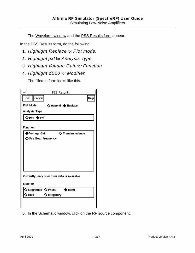
Affirma RF Simulator (SpectreRF) User GuideSimulating Low-Noise Amplifiers
The Waveform window and the PSS Results form appear.
In the PSS Results form, do the following:
1. Highlight Replace for Plot mode.
2. Highlight pxf for Analysis Type.
3. Highlight Voltage Gain for Function.
4. Highlight dB20 for Modifier.
The filled-in form looks like this.
5. In the Schematic window, click on the RF source component.
April 2001 317 Product Version 4.4.6
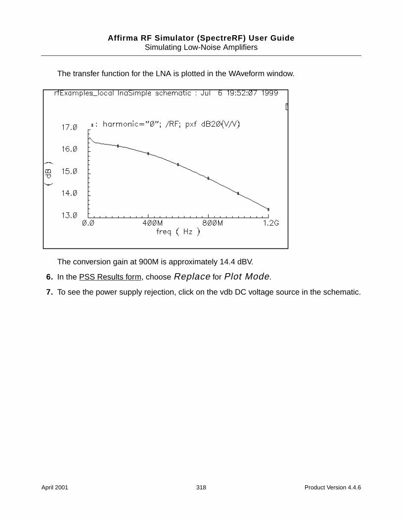
Affirma RF Simulator (SpectreRF) User GuideSimulating Low-Noise Amplifiers
The transfer function for the LNA is plotted in the WAveform window.
The conversion gain at 900M is approximately 14.4 dBV.
6. In the PSS Results form, choose Replace for Plot Mode.
7. To see the power supply rejection, click on the vdb DC voltage source in the schematic.
April 2001 318 Product Version 4.4.6
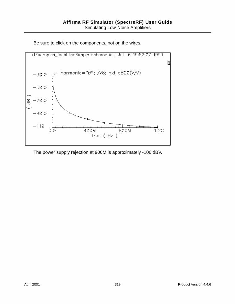
Affirma RF Simulator (SpectreRF) User GuideSimulating Low-Noise Amplifiers
Be sure to click on the components, not on the wires.
The power supply rejection at 900M is approximately -106 dBV.
April 2001 319 Product Version 4.4.6
Affirma RF Simulator (SpectreRF) User Guide
7Simulating Transmission Lines
The Affirma RF simulator can model transmission lines using a quadrature model approach.You can choose between two use models to simulate transmission lines.
Using the LMG Visual Interface independent of the Affirma analog circuit designenvironment
Modeling transmission lines from within the Affirma analog circuit design environment
This chapter shows you the procedures for each use model.
In the first use model, you manually run the Transmission Line Model Generator (LMG) foreach unique transmission line configuration. You create a separate model for each change inline type, geometry, parameters, and operating frequency. After you create the modelsmanually, you instruct the Affirma™ analog circuit design environment to include the resultingexternal model files.
You might want to run LMG manually if you want to see a display of the transmission line crosssection. This cross section display is not currently available as part of the Affirma analogcircuit design environment, but you can call the manual generation procedure from within thedesign environment.You also might want to run LMG manually if you want to share the modelor if you have a circuit with a number of identical transmission line instances. If you run LMGmanually, you create a single model file that can be applied to many instances. If you run LMGcompletely within the Affirma analog circuit design environment, the software creates eachinstance separately.
In the second use model, you run LMG completely within the Affirma analog circuit designenvironment.
Use Model One: Using the LMG Visual Interface
This use model lets you view a cross section of the transmission line you specify. If you modifyyour specifications, the two-dimensional cross-section updates to reflect your changes.
April 2001 320 Product Version 4.4.6
Affirma RF Simulator (SpectreRF) User GuideSimulating Transmission Lines
You start by using LMG to create a lumped-circuit macromodel for each transmission line inthe circuit. For each model, you specify line-parameter information, the length of the line, andthe operating frequencies in the LMG form.
You also specify a unique name for the resulting file that contains the Spectre netlist thatdescribes the subcircuit. It is helpful to use a name that describes the configuration of theparticular transmission line. For example, you might name a stripline of length 1000 with amaximum frequency of 20GHz tline_s1000_20G . (A maximum frequency of 20GHzmeans that the model has diminished accuracy above this value.)
Using your input specifications, LMG automatically generates a quadrature model subcircuitfor each line. The quadrature model subcircuits are only accurate for the length andfrequencies that you specify. If you modify a transmission line, you must rerun LMG for thenew configuration and update the appropriate instances in the schematic to reflect the newLMG output.
When you simulate the circuit, each model file is incorporated into the design by specifyingthe filename as a property on the corresponding tline3 instance(s).
Note: LMG can also create four-terminal transmission line models, but SpectreRF simulationdoes not use these models. For more information about the four-terminal models, see theapplication note “Including Transmission Line Models in Spectre/SpectreRF Simulations inthe 4.4.1 Release.”
Use Model Two: Modeling Transmission Lines Withoutthe Visual Interface
The second use model is easier to use than the first use model. It includes the following steps:
1. Open the schematic.
2. Choose or place a tline3 instance in the schematic.
3. Open the Edit – Properties – Objects form for the transmission line.
4. Describe the transmission line by typing in parameter values. (Units are meters andHertz only.)
5. Repeat steps 2 through 4 for each tline3 instance in the design.
April 2001 321 Product Version 4.4.6
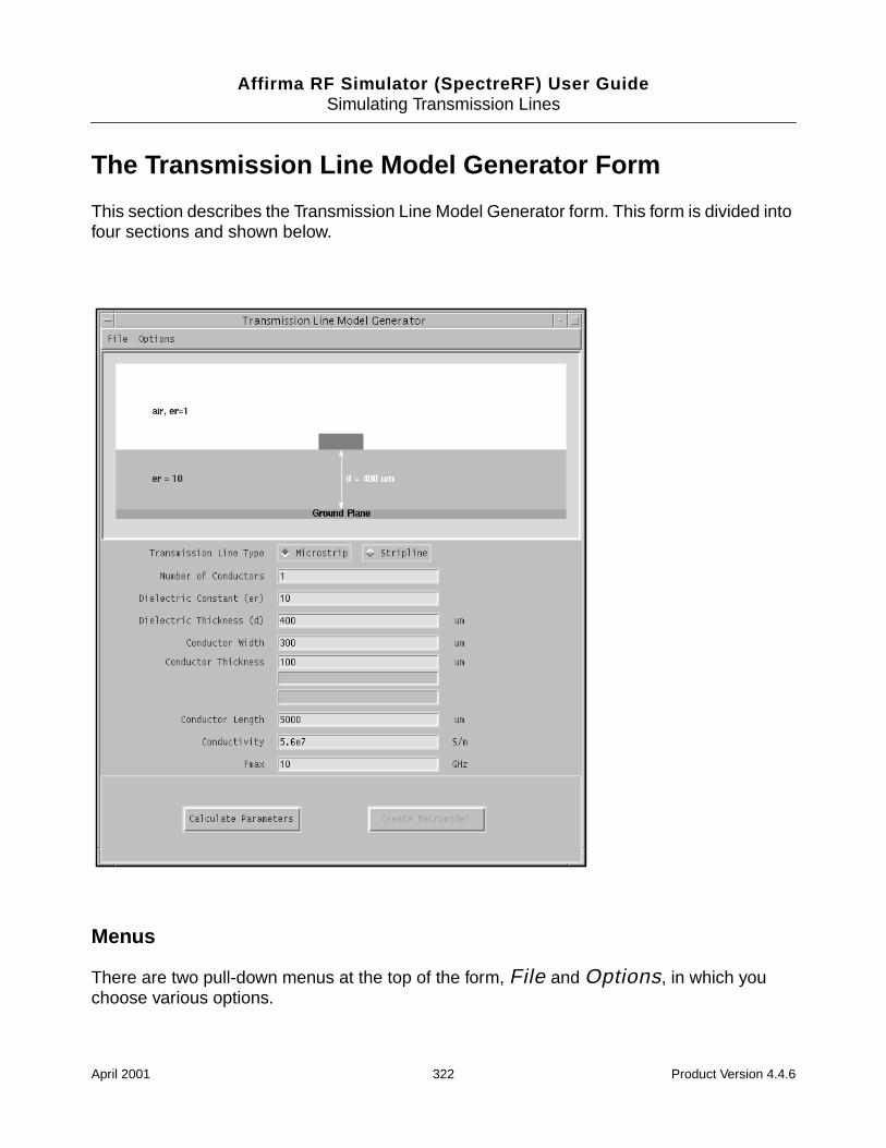
Affirma RF Simulator (SpectreRF) User GuideSimulating Transmission Lines
The Transmission Line Model Generator Form
This section describes the Transmission Line Model Generator form. This form is divided intofour sections and shown below.
Menus
There are two pull-down menus at the top of the form, File and Options, in which youchoose various options.
April 2001 322 Product Version 4.4.6
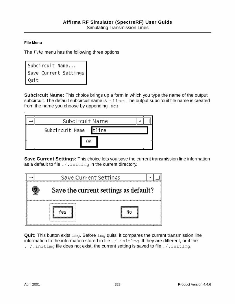
Affirma RF Simulator (SpectreRF) User GuideSimulating Transmission Lines
File Menu
The File menu has the following three options:
Subcircuit Name: This choice brings up a form in which you type the name of the outputsubcircuit. The default subcircuit name is tline . The output subcircuit file name is createdfrom the name you choose by appending.scs.
Save Current Settings: This choice lets you save the current transmission line informationas a default to file ./.initlmg in the current directory.
Quit: This button exits lmg . Before lmg quits, it compares the current transmission lineinformation to the information stored in file ./.initlmg . If they are different, or if the. /.initlmg file does not exist, the current setting is saved to file ./.initlmg .
April 2001 323 Product Version 4.4.6
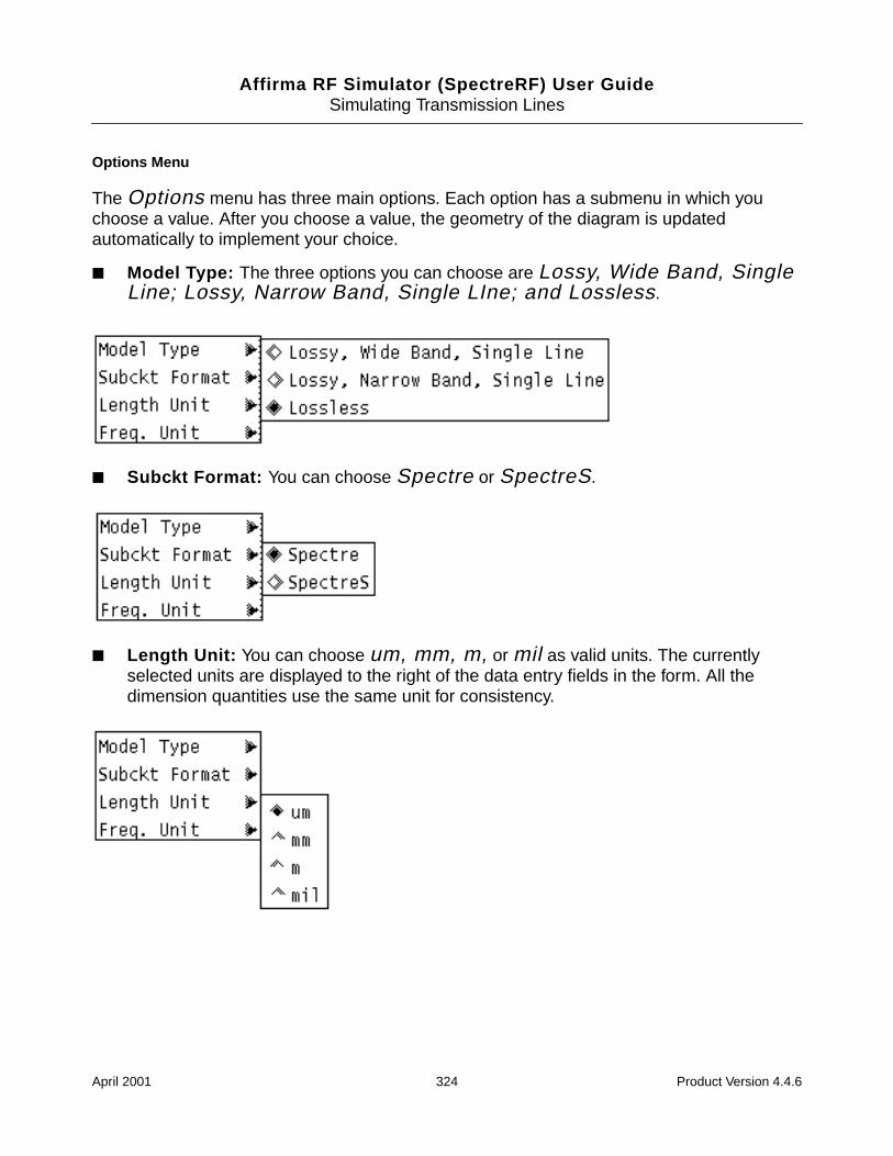
Affirma RF Simulator (SpectreRF) User GuideSimulating Transmission Lines
Options Menu
The Options menu has three main options. Each option has a submenu in which youchoose a value. After you choose a value, the geometry of the diagram is updatedautomatically to implement your choice.
Model Type: The three options you can choose are Lossy, Wide Band, SingleLine; Lossy, Narrow Band, Single LIne; and Lossless.
Subckt Format: You can choose Spectre or SpectreS.
Length Unit: You can choose um, mm, m, or mil as valid units. The currentlyselected units are displayed to the right of the data entry fields in the form. All thedimension quantities use the same unit for consistency.
April 2001 324 Product Version 4.4.6
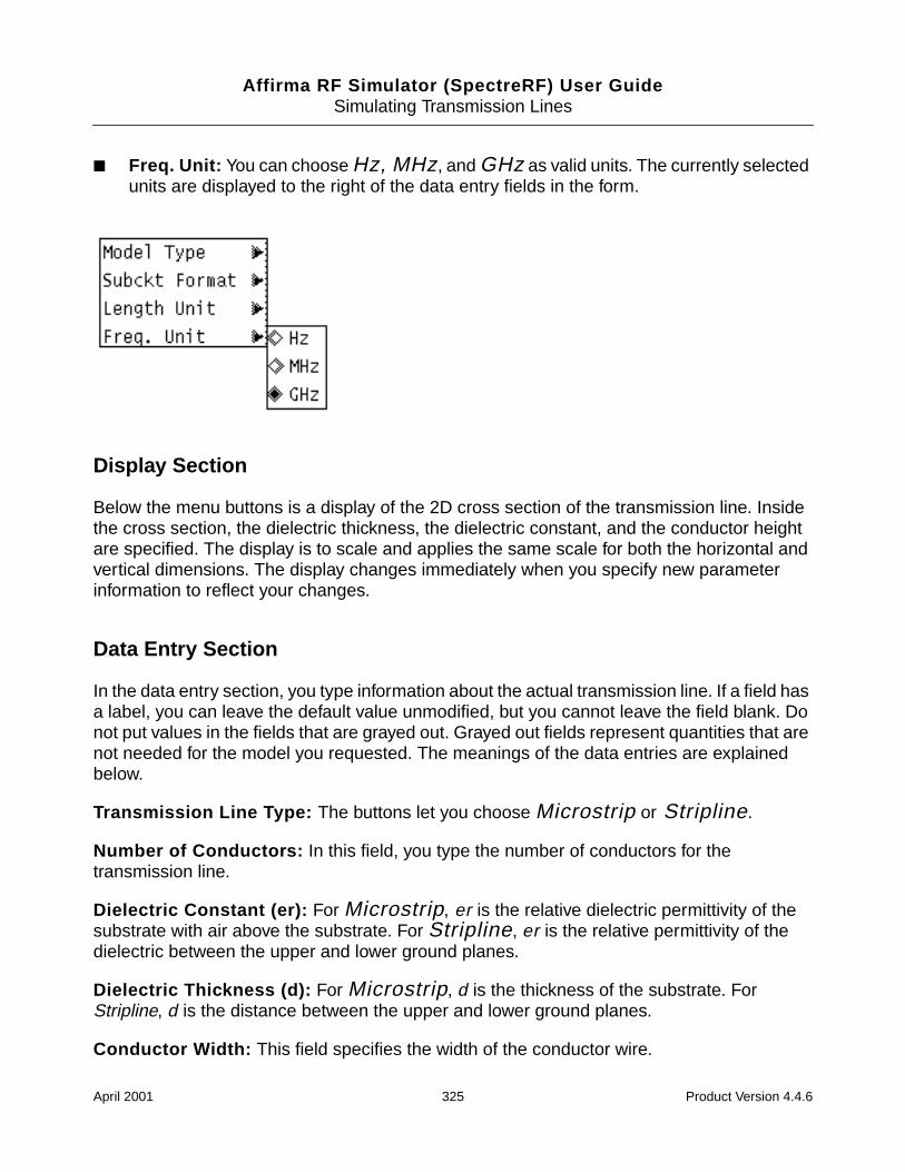
Affirma RF Simulator (SpectreRF) User GuideSimulating Transmission Lines
Freq. Unit: You can choose Hz, MHz, and GHz as valid units. The currently selectedunits are displayed to the right of the data entry fields in the form.
Display Section
Below the menu buttons is a display of the 2D cross section of the transmission line. Insidethe cross section, the dielectric thickness, the dielectric constant, and the conductor heightare specified. The display is to scale and applies the same scale for both the horizontal andvertical dimensions. The display changes immediately when you specify new parameterinformation to reflect your changes.
Data Entry Section
In the data entry section, you type information about the actual transmission line. If a field hasa label, you can leave the default value unmodified, but you cannot leave the field blank. Donot put values in the fields that are grayed out. Grayed out fields represent quantities that arenot needed for the model you requested. The meanings of the data entries are explainedbelow.
Transmission Line Type: The buttons let you choose Microstrip or Stripline.
Number of Conductors: In this field, you type the number of conductors for thetransmission line.
Dielectric Constant (er): For Microstrip, er is the relative dielectric permittivity of thesubstrate with air above the substrate. For Stripline, er is the relative permittivity of thedielectric between the upper and lower ground planes.
Dielectric Thickness (d): For Microstrip, d is the thickness of the substrate. ForStripline, d is the distance between the upper and lower ground planes.
Conductor Width: This field specifies the width of the conductor wire.
April 2001 325 Product Version 4.4.6
Affirma RF Simulator (SpectreRF) User GuideSimulating Transmission Lines
Conductor Thickness: This field specifies the thickness of the conductor wire.
Conductor Height (h): This entry is for Stripline only. It specifies the distance betweenthe lower face of the conductor wire and the upper face of the bottom ground plane.
Conductor Distances: If there are multiple conductors, this field specifies the distancebetween them.
Conductor Length: This field specifies the actual length of the transmission line in the unitshown to the right of the data entry section.
Conductivity: This field specifies the conductivity of the conductor wire. This parameter isused to calculate the DC resistance per meter.
Fmax: The maximum frequency at which the macromodel must work properly. You usuallyset Fmax to the frequency of the highest harmonic that has significant energy in thetransmission line simulations. LMG generates a macromodel of the transmission line that isgood from DC to the value chosen for Fmax.
Function Buttons
The function buttons let you update the figure display, calculate the transmission lineparameters, and create the macromodels. There are two function buttons at the bottom of theTransmission Line Modeler form.
Calculate Parameters: After you specify the 2D transmission line geometry, click on thisbutton to calculate the transmission line parameters. The display shows the characteristicimpedance, propagation velocity, and the DC resistance per meter of the transmission line inthe upper right corner of the form.
Create Macromodel: After you click on the Calculate Parameters button, this buttonis enabled. Click on this button to create the transmission tline model. A pop-up window tellsyou the name of the transmission line model file.
Default Values
When you start lmg , the ./.initlmg file is checked for the defaults. Iffile ./.initlmg does not exist, then the following set of default values is used:
lmgLineType = Microstrip
lmgLengthUnit = um
lmgFreqUnit = GHz
April 2001 326 Product Version 4.4.6
Affirma RF Simulator (SpectreRF) User GuideSimulating Transmission Lines
l mgNumberof Conductors = 1
lmgDielectricPermittivity = 10
lmgDielectricThickness = 400
lmgConductorWidth = 300
lmgConductorDistances = For multiconductors, the width of the firstconductor
lmgConductorThickness = 100
lmgConductorHeight = For multiconductors, the height of the firstconductor
lmgConductorLength = 5000
lmgConductivity = 5.6e7
lmgMaxFreq = 10
lmgSubCircuitName = tline
Example of Modeling a Transmission Line Using LMG
This section presents an example of modeling a transmission line using the TransmissionLine Model Generator form following the first use model. Because the microstrip and striplineprocedures are very similar, only a stripline example is shown here.
Setup
Before you run lmg, you must set up the executables correctly. You must install the Spectreor SpectreRF circuit simulator, and also Coeffgen, with the correct path set.
Creating the Transmission Line Model
To model the transmission line, perform the following steps:
1. Choose Tools – RF – Transmission Line Modeler in the Simulation Window or typelmg from the UNIX command line.
April 2001 327 Product Version 4.4.6
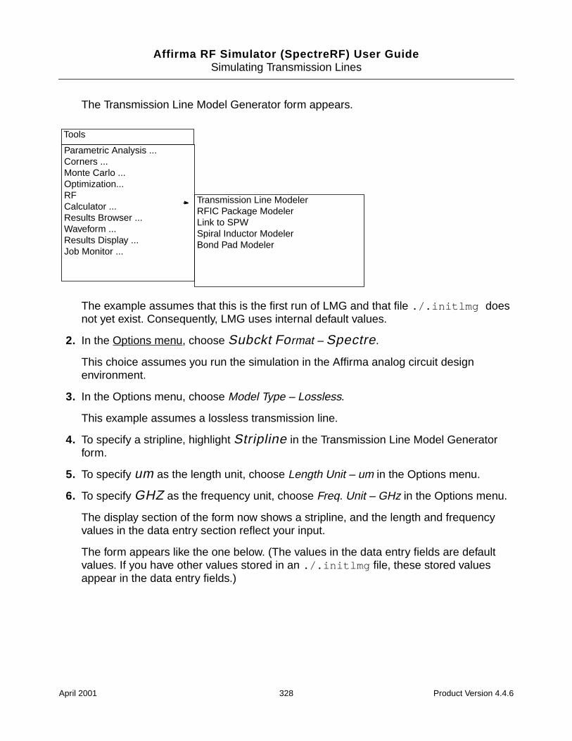
Affirma RF Simulator (SpectreRF) User GuideSimulating Transmission Lines
The Transmission Line Model Generator form appears.
The example assumes that this is the first run of LMG and that file ./.initlmg doesnot yet exist. Consequently, LMG uses internal default values.
2. In the Options menu, choose Subckt Format – Spectre.
This choice assumes you run the simulation in the Affirma analog circuit designenvironment.
3. In the Options menu, choose Model Type – Lossless.
This example assumes a lossless transmission line.
4. To specify a stripline, highlight Stripline in the Transmission Line Model Generatorform.
5. To specify um as the length unit, choose Length Unit – um in the Options menu.
6. To specify GHZ as the frequency unit, choose Freq. Unit – GHz in the Options menu.
The display section of the form now shows a stripline, and the length and frequencyvalues in the data entry section reflect your input.
The form appears like the one below. (The values in the data entry fields are defaultvalues. If you have other values stored in an ./.initlmg file, these stored valuesappear in the data entry fields.)
Parametric Analysis ...Corners ...Monte Carlo ...Optimization...RFCalculator ...Results Browser ...Waveform ...Results Display ...Job Monitor ...
Transmission Line ModelerRFIC Package ModelerLink to SPWSpiral Inductor ModelerBond Pad Modeler
Tools
April 2001 328 Product Version 4.4.6
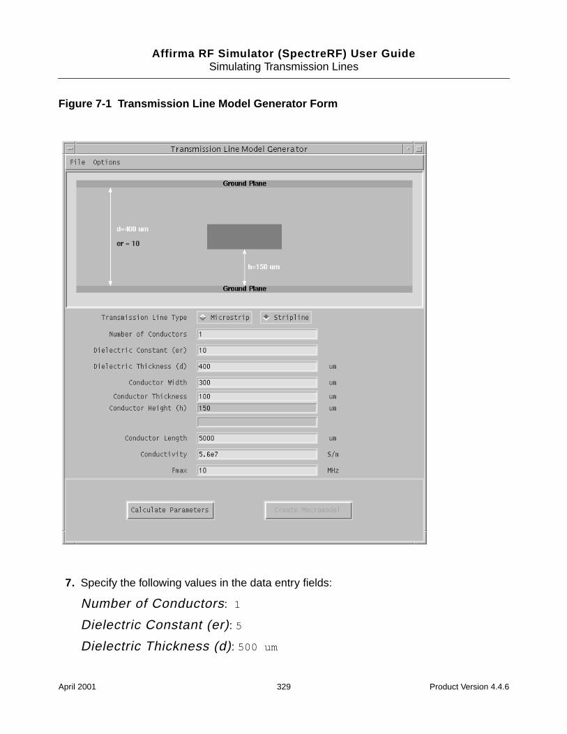
Affirma RF Simulator (SpectreRF) User GuideSimulating Transmission Lines
Figure 7-1 Transmission Line Model Generator Form
7. Specify the following values in the data entry fields:
Number of Conductors: 1
Dielectric Constant (er): 5
Dielectric Thickness (d): 500 um
April 2001 329 Product Version 4.4.6

Affirma RF Simulator (SpectreRF) User GuideSimulating Transmission Lines
Conductor Width: 200 um
Conductor Thickness: 50 um
Conductor Height (h): 225 um
Conductor Length: 1000 um
Conductivity: 5.6e7
Fmax: 20
The macromodel is created using the Gaussian quadrature algorithm[1]. This model isusable only below a certain frequency.
Generally, the higher the order of the quadrature, the wider the useful band width. Theorder of the quadrature is chosen so that the magnitude of the transmission coefficientof the equivalent transmission line is no less than 97.5 percent at the highestnonnegligible frequency. One way to determine this frequency is to use harmonics. Giventhe fundamental frequency of the signal and the number of harmonics, Fmax equalsthe fundamental frequency multiplied by the highest harmonic number.
For this example, the value of Fmax assumes a fundamental frequency of2 GHZ with 10 harmonics considered. The Fmax value is (2x10) GHz.
8. Click on the Calculate Parameters function button.
This step calculates the characteristic impedance, the propagation velocity, the DCresistance per meter, the corner frequency of the conductor, and the time delay of thetransmission line. The display section changes to reflect the values you specified, andthe calculated parameters appear in the top right corner of the display section. At thispoint, the Create Macromodel button is enabled.
April 2001 330 Product Version 4.4.6
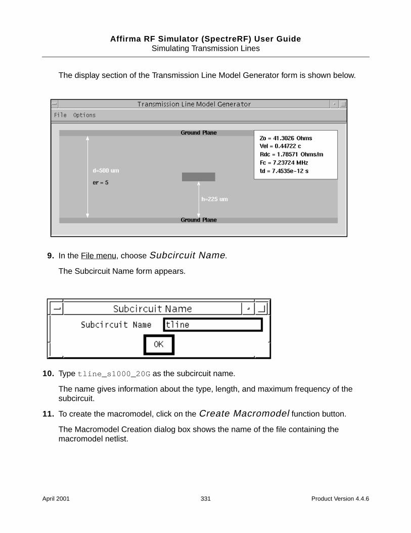
Affirma RF Simulator (SpectreRF) User GuideSimulating Transmission Lines
The display section of the Transmission Line Model Generator form is shown below.
9. In the File menu, choose Subcircuit Name.
The Subcircuit Name form appears.
10. Type tline_s1000_20G as the subcircuit name.
The name gives information about the type, length, and maximum frequency of thesubcircuit.
11. To create the macromodel, click on the Create Macromodel function button.
The Macromodel Creation dialog box shows the name of the file containing themacromodel netlist.
April 2001 331 Product Version 4.4.6
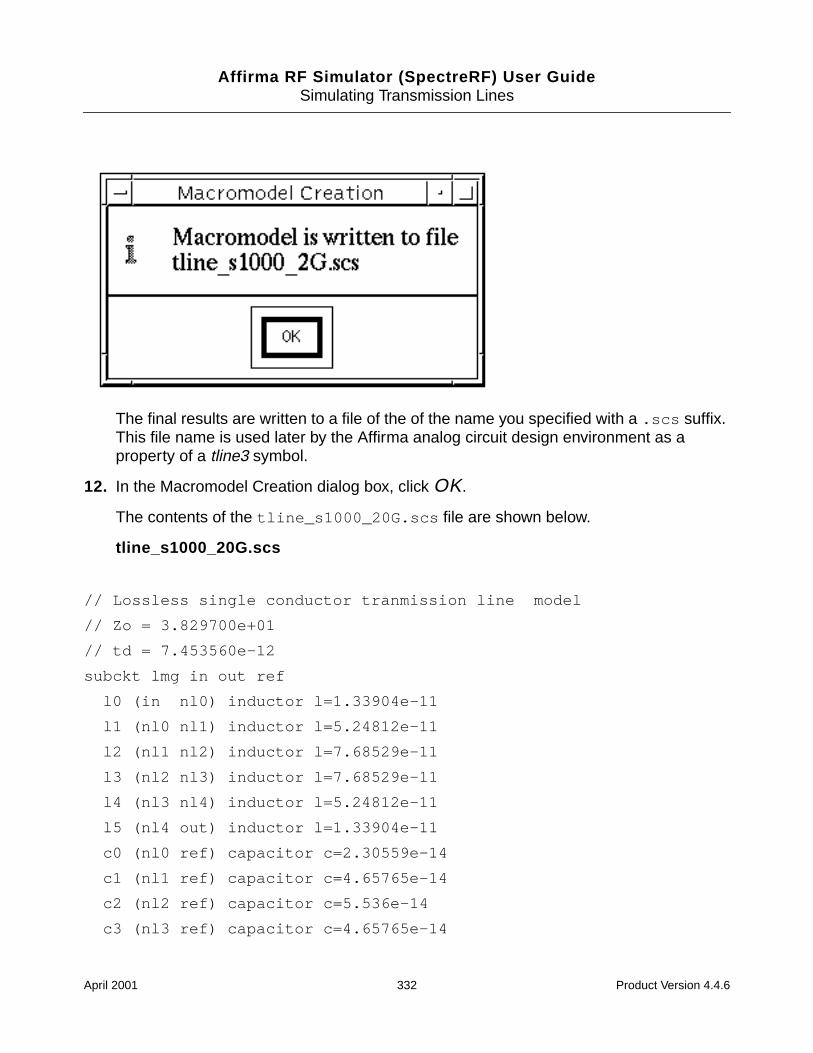
Affirma RF Simulator (SpectreRF) User GuideSimulating Transmission Lines
The final results are written to a file of the of the name you specified with a .scs suffix.This file name is used later by the Affirma analog circuit design environment as aproperty of a tline3 symbol.
12. In the Macromodel Creation dialog box, click OK.
The contents of the tline_s1000_20G.scs file are shown below.
tline_s1000_20G.scs
// Lossless single conductor tranmission line model
// Zo = 3.829700e+01
// td = 7.453560e-12
subckt lmg in out ref
l0 (in nl0) inductor l=1.33904e-11
l1 (nl0 nl1) inductor l=5.24812e-11
l2 (nl1 nl2) inductor l=7.68529e-11
l3 (nl2 nl3) inductor l=7.68529e-11
l4 (nl3 nl4) inductor l=5.24812e-11
l5 (nl4 out) inductor l=1.33904e-11
c0 (nl0 ref) capacitor c=2.30559e-14
c1 (nl1 ref) capacitor c=4.65765e-14
c2 (nl2 ref) capacitor c=5.536e-14
c3 (nl3 ref) capacitor c=4.65765e-14
April 2001 332 Product Version 4.4.6
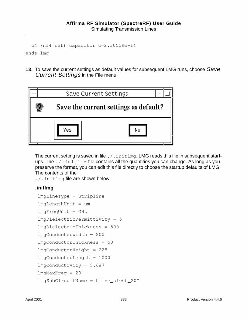
Affirma RF Simulator (SpectreRF) User GuideSimulating Transmission Lines
c4 (nl4 ref) capacitor c=2.30559e-14
ends lmg
13. To save the current settings as default values for subsequent LMG runs, choose SaveCurrent Settings in the File menu.
The current setting is saved in file ./.initlmg . LMG reads this file in subsequent start-ups. The ./.initlmg file contains all the quantities you can change. As long as youpreserve the format, you can edit this file directly to choose the startup defaults of LMG.The contents of the./.initlmg file are shown below.
.initlmg
lmgLineType = Stripline
lmgLengthUnit = um
lmgFreqUnit = GHz
lmgDielectricPermittivity = 5
lmgDielectricThickness = 500
lmgConductorWidth = 200
lmgConductorThickness = 50
lmgConductorHeight = 225
lmgConductorLength = 1000
lmgConductivity = 5.6e7
lmgMaxFreq = 20
lmgSubCircuitName = tline_s1000_20G
April 2001 333 Product Version 4.4.6
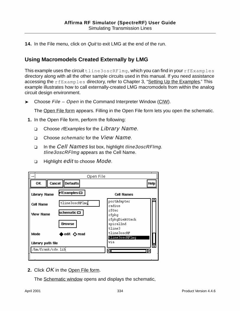
Affirma RF Simulator (SpectreRF) User GuideSimulating Transmission Lines
14. In the File menu, click on Quit to exit LMG at the end of the run.
Using Macromodels Created Externally by LMG
This example uses the circuit tline3oscRFlmg , which you can find in your rfExamplesdirectory along with all the other sample circuits used in this manual. If you need assistanceaccessing the rfExamples directory, refer to Chapter 3, “Setting Up the Examples.” Thisexample illustrates how to call externally-created LMG macromodels from within the analogcircuit design environment.
Choose File – Open in the Command Interpreter Window (CIW).
The Open File form appears. Filling in the Open File form lets you open the schematic.
1. In the Open File form, perform the following:
Choose rfExamples for the Library Name.
Choose schematic for the View Name.
In the Cell Names list box, highlight tline3oscRFlmg.tline3oscRFlmg appears as the Cell Name.
Highlight edit to choose Mode.
2. Click OK in the Open File form.
The Schematic window opens and displays the schematic,
April 2001 334 Product Version 4.4.6
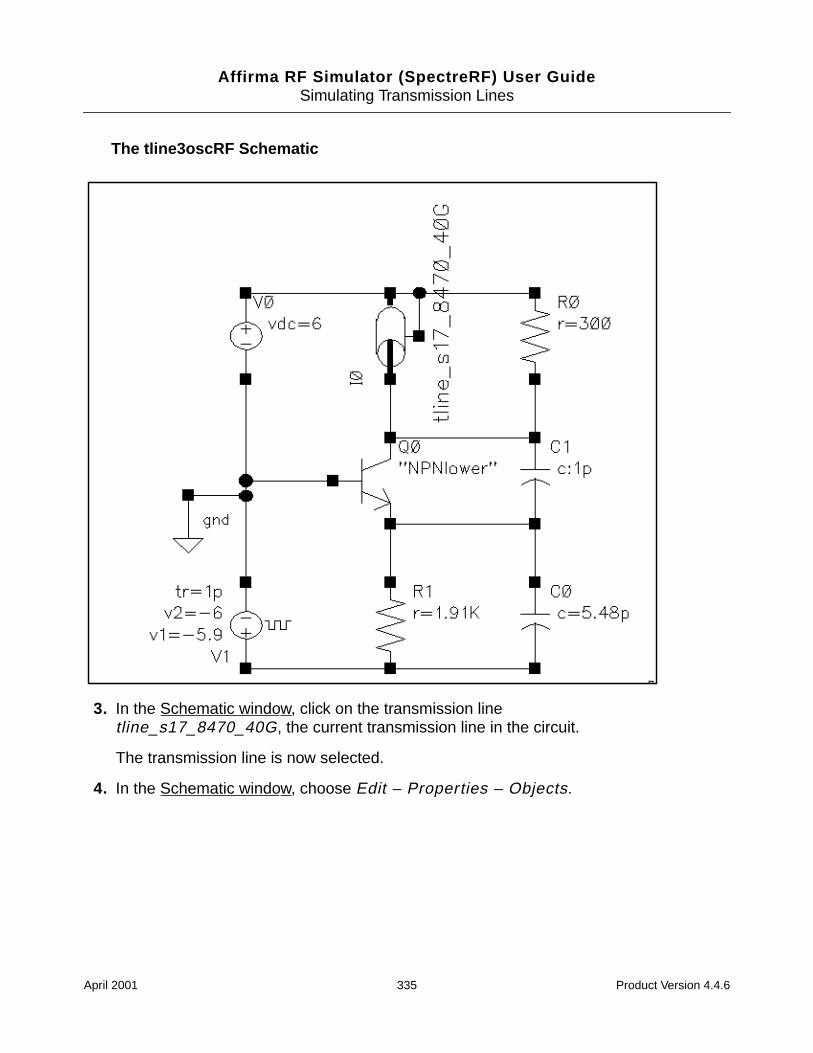
Affirma RF Simulator (SpectreRF) User GuideSimulating Transmission Lines
The tline3oscRF Schematic
3. In the Schematic window, click on the transmission linetline_s17_8470_40G, the current transmission line in the circuit.
The transmission line is now selected.
4. In the Schematic window, choose Edit – Properties – Objects.
April 2001 335 Product Version 4.4.6
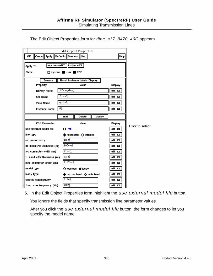
Affirma RF Simulator (SpectreRF) User GuideSimulating Transmission Lines
The Edit Object Properties form for tline_s17_8470_40G appears.
5. In the Edit Object Properties form, highlight the use external model file button.
You ignore the fields that specify transmission line parameter values.
After you click the use external model file button, the form changes to let youspecify the model name.
Click to select.
April 2001 336 Product Version 4.4.6
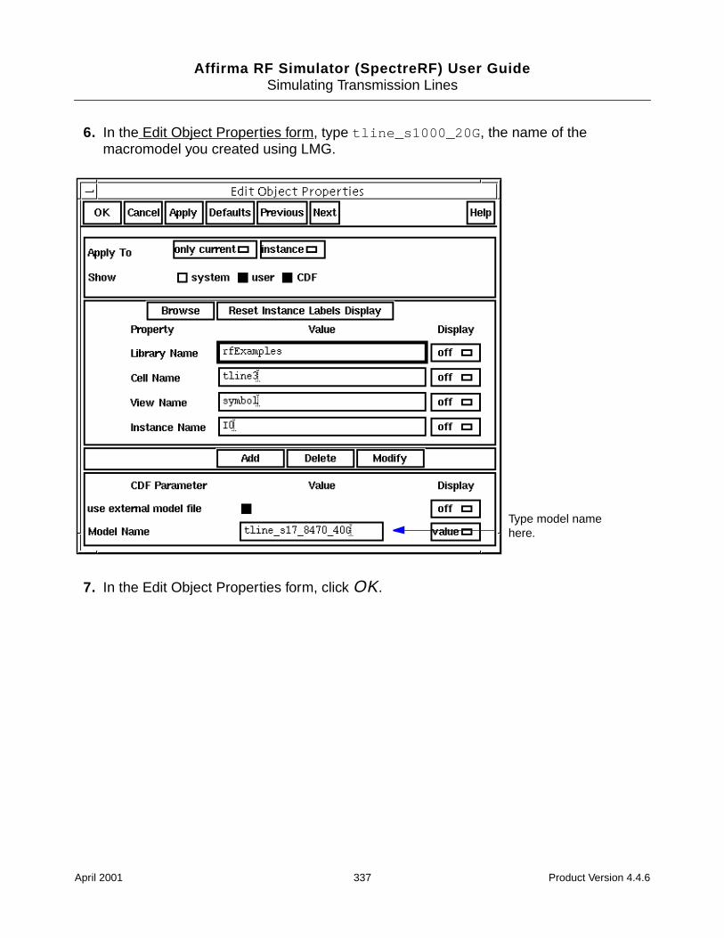
Affirma RF Simulator (SpectreRF) User GuideSimulating Transmission Lines
6. In the Edit Object Properties form, type tline_s1000_20G , the name of themacromodel you created using LMG.
7. In the Edit Object Properties form, click OK.
Type model namehere.
April 2001 337 Product Version 4.4.6
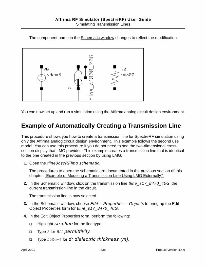
Affirma RF Simulator (SpectreRF) User GuideSimulating Transmission Lines
The component name in the Schematic window changes to reflect the modification.
You can now set up and run a simulation using the Affirma analog circuit design environment.
Example of Automatically Creating a Transmission Line
This procedure shows you how to create a transmission line for SpectreRF simulation usingonly the Affirma analog circuit design environment. This example follows the second usemodel. You can use this procedure if you do not need to see the two-dimensional cross-section display that LMG provides. This example creates a transmission line that is identicalto the one created in the previous section by using LMG.
1. Open the tline3oscRFlmg schematic.
The procedures to open the schematic are documented in the previous section of thischapter, “Example of Modeling a Transmission Line Using LMG Externally.”
2. In the Schematic window, click on the transmission line tline_s17_8470_40G, thecurrent transmission line in the circuit.
The transmission line is now selected.
3. In the Schematic window, choose Edit – Properties – Objects to bring up the EditObject Properties form for tline_s17_8470_40G.
4. In the Edit Object Properties form, perform the following:
Highlight stripline for the line type.
Type 5 for er: permittivity.
Type 500e-6 for d: dielectric thickness (m).
April 2001 338 Product Version 4.4.6
Affirma RF Simulator (SpectreRF) User GuideSimulating Transmission Lines
Note: Notice that you enter values for this form in meters and Hertz.
Type 200e-6 for w: conductor width.
Type 5e-6 for t: conductor thickness (m).
Type 5e-6 for h: conductor height (m).
Type 1e-3 for len: conductor length (m)
Highlight lossless for the model type.
Note: If you choose lossy for the model type, two additional fields open to let you specifythe lossy type and conductivity.
Type 40e9 for freq: max frequency (Hz).
For an explanation of this value see page 16 in the procedure for modelingtransmission lines using LMG.
April 2001 339 Product Version 4.4.6
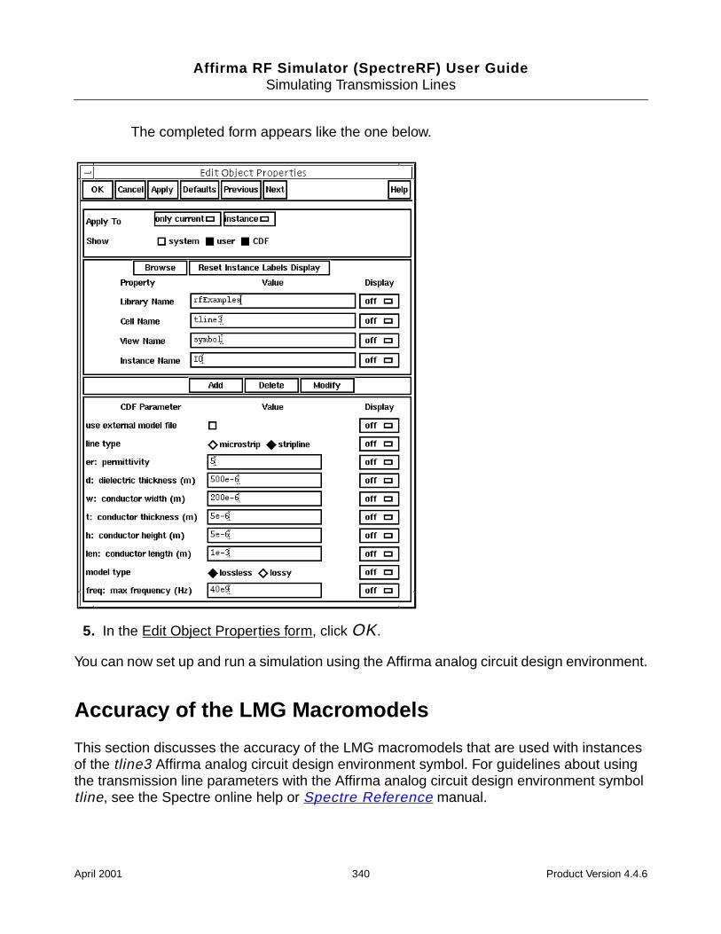
Affirma RF Simulator (SpectreRF) User GuideSimulating Transmission Lines
The completed form appears like the one below.
5. In the Edit Object Properties form, click OK.
You can now set up and run a simulation using the Affirma analog circuit design environment.
Accuracy of the LMG Macromodels
This section discusses the accuracy of the LMG macromodels that are used with instancesof the tline3 Affirma analog circuit design environment symbol. For guidelines about usingthe transmission line parameters with the Affirma analog circuit design environment symboltline, see the Spectre online help or Spectre Reference manual.
April 2001 340 Product Version 4.4.6
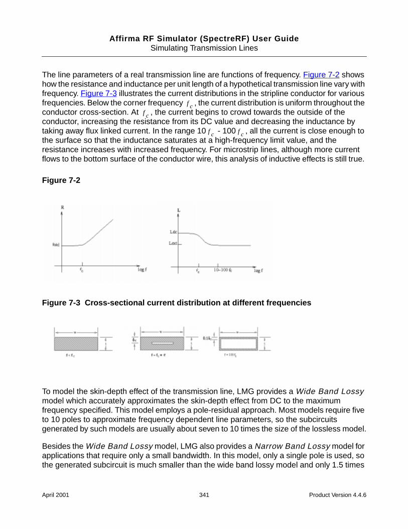
Affirma RF Simulator (SpectreRF) User GuideSimulating Transmission Lines
The line parameters of a real transmission line are functions of frequency. Figure 7-2 showshow the resistance and inductance per unit length of a hypothetical transmission line vary withfrequency. Figure 7-3 illustrates the current distributions in the stripline conductor for variousfrequencies. Below the corner frequency , the current distribution is uniform throughout theconductor cross-section. At , the current begins to crowd towards the outside of theconductor, increasing the resistance from its DC value and decreasing the inductance bytaking away flux linked current. In the range 10 - 100 , all the current is close enough tothe surface so that the inductance saturates at a high-frequency limit value, and theresistance increases with increased frequency. For microstrip lines, although more currentflows to the bottom surface of the conductor wire, this analysis of inductive effects is still true.
Figure 7-2
Figure 7-3 Cross-sectional current distribution at different frequencies
To model the skin-depth effect of the transmission line, LMG provides a Wide Band Lossymodel which accurately approximates the skin-depth effect from DC to the maximumfrequency specified. This model employs a pole-residual approach. Most models require fiveto 10 poles to approximate frequency dependent line parameters, so the subcircuitsgenerated by such models are usually about seven to 10 times the size of the lossless model.
Besides the Wide Band Lossy model, LMG also provides a Narrow Band Lossy model forapplications that require only a small bandwidth. In this model, only a single pole is used, sothe generated subcircuit is much smaller than the wide band lossy model and only 1.5 times
f cf c
f c f c
April 2001 341 Product Version 4.4.6
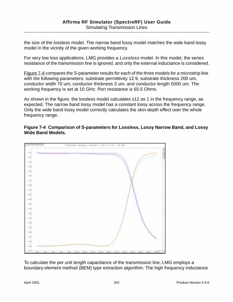
Affirma RF Simulator (SpectreRF) User GuideSimulating Transmission Lines
the size of the lossless model. The narrow band lossy model matches the wide band lossymodel in the vicinity of the given working frequency.
For very low loss applications, LMG provides a Lossless model. In this model, the seriesresistance of the transmission line is ignored, and only the external inductance is considered.
Figure 7-4 compares the S-parameter results for each of the three models for a microstrip linewith the following parameters: substrate permittivity 12.9, substrate thickness 200 um,conductor width 70 um, conductor thickness 3 um, and conductor length 5000 um. Theworking frequency is set at 10 GHz. Port resistance is 65.5 Ohms.
As shown in the figure, the lossless model calculates s12 as 1 in the frequency range, asexpected. The narrow band lossy model has a constant lossy across the frequency range.Only the wide band lossy model correctly calculates the skin-depth effect over the wholefrequency range.
Figure 7-4 Comparison of S-parameters for Lossless, Lossy Narrow Band, and LossyWide Band Models.
To calculate the per unit length capacitance of the transmission line, LMG employs aboundary-element method (BEM) type extraction algorithm. The high frequency inductance
April 2001 342 Product Version 4.4.6
Affirma RF Simulator (SpectreRF) User GuideSimulating Transmission Lines
per unit length is calculated by assuming the current flows on the surface of the conductor,an appropriate assumption for RF simulations as shown above. The extraction algorithm hasan error of less than 1 percent.
For the macromodel, LMG uses a nonuniform Gaussian quadrature algorithm.
Figure 7-5 shows the frequency response of nonuniform and uniform lumping for a striplinewith the conductor length set to 6000 um. Both models use eight LC lumps to approximatethe transmission line. Figure 7-5 shows that within the bandwidth, the reflection coefficient ofthe nonuniform lumping is below 1 percent, but the uniform lumping causes much morereflection. For the same number of lumps, the nonuniform case has a much wider bandwidth.For the same accuracy, nonuniform lumping requires fewer lumps than uniform lumping.
By requiring the transmission coefficient to be above 0.975, the Gaussian nonuniformlumping requires an average of five lumps per wavelength, while the macromodel requires 8-10 lumps per wavelength. For the current version of LMG, the highest order allowed is 30,equivalent to six wavelengths at the maximum frequency. For longer lines, divide the line intosections shorter than six wavelengths. Then apply LMG to generate macromodels for eachsection.
April 2001 343 Product Version 4.4.6
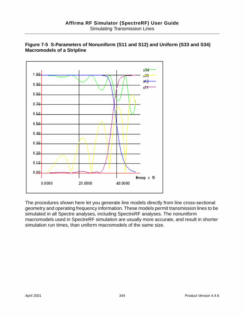
Affirma RF Simulator (SpectreRF) User GuideSimulating Transmission Lines
Figure 7-5 S-Parameters of Nonuniform (S11 and S12) and Uniform (S33 and S34)Macromodels of a Stripline
The procedures shown here let you generate line models directly from line cross-sectionalgeometry and operating frequency information. These models permit transmission lines to besimulated in all Spectre analyses, including SpectreRF analyses. The nonuniformmacromodels used in SpectreRF simulation are usually more accurate, and result in shortersimulation run times, than uniform macromodels of the same size.
April 2001 344 Product Version 4.4.6
Affirma RF Simulator (SpectreRF) User Guide
8Modeling RF IC Packages
As the working frequency of RF devices in PCS and wireless communications increases, theeffect of the RF IC package parasitics, like reflection caused by impedance mismatch, highfrequency resonances, and crosstalk among pins and bond wires, becomes important.Accurate simulation of the systems requires accurate modeling of these parasitics.
There are many IC package types, but more than 95 percent of commercial products use non-routable packages such as the small outline IC (SOIC), quad flat pack (QFP), and dual inlinepackage (DIP) families. PKG, an RF IC package modeler, has been developed based on thisinformation.
The PKG core algorithm contains the following four building blocks: the package physicalgeometry modeling block, mesh making for EM solvers, 3D EM solvers for capacitance andinductance calculations, and a post processing block for creating the macromodel and dieattach terminal.
To set up the physical geometry, you must specify the following:
Package dimensions, including the dimensions of the package body
Die cavity size
External part of the lead frame
Internal lead frame setup
Die attach setup
Bond wire setup
PKG supports the following package families:
SOIC families including shrunken small outline IC (SSOP), thin shrunken small outlineIC (TSSOP), very small outline IC (VSO) and others
QFP families, including TQFP and LQFP
DIP families
April 2001 345 Product Version 4.4.6
Affirma RF Simulator (SpectreRF) User GuideModeling RF IC Packages
PKG supports both the gull-wing pin and J-pin types.
The mesh-making function is based on the physical modeling block. The regularity of theactual package geometry permits the creation of high-quality mesh for higher efficiency andfaster convergence. You can control the mesh to satisfy your accuracy requirements.
In the EM solver, Fastcap and Fasthenry are the capacitance and inductance solvers,respectively. Because the mesh-making module is relatively independent of the solvers, newsolvers can be added to the current ones.
The postprocessing block takes the capacitance and inductance results from the EM solversas input and generates macromodels. The supported macromodel types are Spectre,SpectreS and Spice.
The graphical user interface (GUI) consists of the main window and five additional windowsfor geometry modeling and setup of solution parameters. The GUI also lets you import thelead frame and bond wire data that you can extract from the layout data or library.
For information about specific topics, consult the subsections below:
“The Four PKG Building Blocks” section on page 347 explains the four basic buildingblocks of PKG.
The “PKG Setup Requirements” section on page 350 explains the license and filerequirements to set up and run PKG.
“The PKG RF IC Package Modeler Window” section on page 351 explains the mainwindow of the PKG GUI.
The “Package Dimension Setup” section on page 355 explains how to set up the generalpackage parameters such as the package body and the external lead frame dimensions.
The “Die Attach Setup” section on page 361 explains the die attach setup.
The “Internal Lead Frame Setup” section on page 362 explains the details of the setupof the internal pin leads and the export and import of lead frame files.
The “Bond Wire Setup” section on page 367 explains the details of how to set up thebond wires and how to export and import bond wire files.
The “Parameter Extraction” section on page 372 tells you about issues concerning thecalculation of the capacitance, resistance, and inductance parameters.
The “Macromodel Generation” section on page 377 explains the schematic of themacromodel and the generation of macromodels for SpectreRF simulations includingmacromodel name and type, and it should include an optional die attach terminal.
April 2001 346 Product Version 4.4.6
Affirma RF Simulator (SpectreRF) User GuideModeling RF IC Packages
The “Accuracy Analysis” section on page 381 explains accuracy limits and issues thataffect the PKG accuracy.
The “Simulation of Package Models in the Affirma Analog Circuit Design Environment”section on page 381 explains the Affirma™ analog circuit design environment symbol forthe RF package model and how to simulate RF IC packages in the design environment.
The Four PKG Building Blocks
The four large building blocks in PKG are
Setup for package physical geometry modeling
Mesh making for EM solvers
The EM solvers
The postprocessor.
Most of the physical geometry modeling is done with the PKG GUI, the rest is done with thePKG core algorithms.
Package Physical Geometry Modeling
PKG models the following three families of non-routable IC packages:
The small outline IC (SOIC) family, including varieties like the shrunken small outline IC(SSOP), the thin shrunken small outline (TSSOP), and the very small out line IC (VSO)
The quad flat pack (QFP) family, including LQFP, TQFP and others
The dual inline package (DIP) family
The SOIC and QFT packages can have gull-wing or J-pin types. Each of these packagescontain the following four components:
The package body, which is often plastic or ceramic
The lead frame, which includes the pins and die attach
The bond wires
The die
The die is modeled separately from the package model because it contains the actual circuits.The whole package geometry setup is divided into three steps: the package general
April 2001 347 Product Version 4.4.6
Affirma RF Simulator (SpectreRF) User GuideModeling RF IC Packages
dimension setup, in which you specify the general dimension parameters; the internal leadframe setup, which includes both the pins and the die attach; and the bond wire setup.
Package General Dimension Setup
The package general dimension parameters include the dimensions of the package body, thedie cavity and the external lead frame. The package body dimensions are length, width, andthickness. Because the die cavity is assumed to be located at the center of the package, youspecify only its length, its width, and the bonding pad height, which is used to determine theheight of the bonding pads. Because the external lead frame is usually standard, you set upall the pins using dimensions such as pin pitch, pin width, and pin thickness. However, forirregular packages, you can override these parameters for individual pins in the internal leadframe setup stage.
Internal Lead Frame Setup
The internal lead frame includes the die attach and the pins. The die attach is approximatedwith a rectangular plate placed at the center of the package. You must specify its length,width, thickness, and elevation.
The internal portion of the pins are approximated using a three-segment model. The firstsegment connects to the external part of the pin, and the third segment is where the bondwires are attached. The second segment, connecting the first and the third segment, isgenerated automatically from the first and the third segment data. You specify the first andthird segments by their location, length, and width. The location of the first segment takes thestandard values as specified by the pin pitch and pin width. You can override these data forspecial packages. You can also choose Using Symmetry to speed the setup.
Bond Wire Setup
You specify each bond wire by its length, the coordinates of its two end points, and its shapefunction. You can choose between two shape functions. One is quadratic, and the other is anexponential-distribution-like function. Each function is determined by three parameters, andthese parameters are determined by the length and the two end points of the bond wire.
There are three types of bond wire connection. They are pin to die connection, pin to da downbonding, and die to da down bonding.
You can specify double and multiple bonding with bond wires of different lengths andthicknesses.
April 2001 348 Product Version 4.4.6
Affirma RF Simulator (SpectreRF) User GuideModeling RF IC Packages
EM Solvers and Mesh Making
Capacitance Calculation
Because the RF IC package is usually electrically small at RF frequencies, the quasi-staticapproach creates a relatively accurate model, in which the capacitance, the inductance, andthe resistance are the parameters of interest. Fastcap is used to calculate the package.Fastcap is a multipole, accelerated boundary element solver that solves the capacitance ofthe lead frame by calculating the electric charge distribution on the conductor surfaces andon the dielectric interfaces that are discretized into quadrilaterals. The edge effects of theelectric charge distribution are modeled using a nonuniform mesh. The ground plane isapproximated with a finite-sized rectangular plate when simulating the ground plane effect.Because the size of the bond wires are very small compared to the lead frame, they areignored in the capacitance calculation. PKG provides three accuracy levels that use meshesof different density.
Inductance Calculation
Fasthenry is used to calculate the inductance and resistance of the pins and bond wires.Fasthenry is a PEEC-like (partial element equivalent circuit) solver with multipoleacceleration. Because of the skin-depth effect, the inductance and resistance are frequencydependent and must be evaluated at each frequency point.
For packages with a large pin count number, evaluating the skin-depth effect at a relativelyhigh frequency is very difficult. Because the skin-depth effect mainly affects the self-resistance and self-inductance, a two-step approach can reduce the computational difficulty.Because the mutual resistance is negligible and the mutual inductance does not changemuch with frequency, the mutual inductance is evaluated at the corner frequency, which isdefined as the frequency at which the skin depth equals the pin thickness. The self-inductance and resistance are corrected at the working frequency by calculating theinductance and resistance of each pin separately. The results of the two steps are thencombined together to create the impedance matrix at the working frequency.
Macromodel Generation
The fourth component of the package modeler is the post processor. The post processorcreates the macromodel using data extracted from the capacitance and inductancecalculations and creates the die attach terminal.
April 2001 349 Product Version 4.4.6
Affirma RF Simulator (SpectreRF) User GuideModeling RF IC Packages
Because SpectreRF simulations produce time-domain solutions, the macromodel must bephysical. The macromodel also must be adapted to SpectreRF simulations to avoid slowdownby high-frequency resonances.
For details about the macromodels, refer to the “Macromodel Generation” section onpage 377.
PKG Setup Requirements
Before running PKG, you must have the license, the executable, proper installation of therequired files, and appropriate settings of the bin path.
License Checking
PKG checks for its own license.
Executables
The required executables are pkg , fastcap , and fasthenry . You must install them at$CDSHOME/tools/dfII/bin .
PKG GUI Files
The PKG GUI files are the following encrypted tcl files:
Initialization Files
The two required initialization files are
init.pkg
init.coeffgen
You must install them at $CDSHOME/tools/dfII/etc/pkg
pkgGUI.pkg pkgDimensionSetup.pkg
pkgLeadframeSetup.pkg pkgBondwireSetup.pkg
pkgFileIO.pkg pkgSolve.pkg
April 2001 350 Product Version 4.4.6
Affirma RF Simulator (SpectreRF) User GuideModeling RF IC Packages
There are two more optional initialization files.
~/.pkginit , which is installed in the user’s home directory.
./.pkginit , which is installed at the current working directory.
When you start PKG, the initialization files, if they exist, are sourced in the following order:
1. $CDSHOME/tools/dfII/etc/pkg/init.pkg
2. ~/.initpkg
3. ./.initpkg
If a variable is set more than once, it takes the last set value.
Running pkg
PKG requires a working directory for the project. Usually the project name is the appropriatesubdirectory name. If you do not specify a project name, the default subdirectory calledpkg.proj is the working directory.
You can start PKG by performing the following command:
In the Simulation Window, choose Tools – RF – IC Package Modeler.
Or
Type pkg <projectName> in a terminal window.
The PKG RF IC Package Modeler Window
As shown in Figure 8-1 below, the RF IC Package Modeler form of the PKG GUI contains thetwo sections described in the bulleted list below:
April 2001 351 Product Version 4.4.6
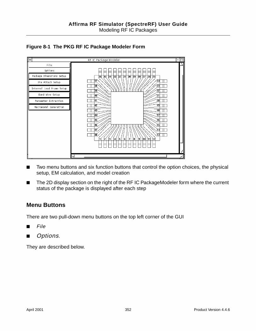
Affirma RF Simulator (SpectreRF) User GuideModeling RF IC Packages
Figure 8-1 The PKG RF IC Package Modeler Form
Two menu buttons and six function buttons that control the option choices, the physicalsetup, EM calculation, and model creation
The 2D display section on the right of the RF IC PackageModeler form where the currentstatus of the package is displayed after each step
Menu Buttons
There are two pull-down menu buttons on the top left corner of the GUI
File
Options.
They are described below.
April 2001 352 Product Version 4.4.6
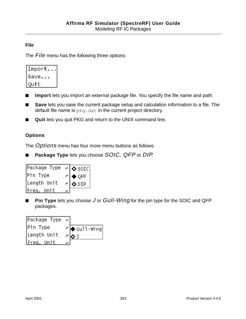
Affirma RF Simulator (SpectreRF) User GuideModeling RF IC Packages
File
The File menu has the following three options:
Import lets you import an external package file. You specify the file name and path.
Save lets you save the current package setup and calculation information to a file. Thedefault file name is pkg.dat in the current project directory.
Quit lets you quit PKG and return to the UNIX command line.
Options
The Options menu has four more menu buttons as follows.
Package Type lets you choose SOIC, QFP or DIP.
Pin Type lets you choose J or Gull-Wing for the pin type for the SOIC and QFPpackages.
April 2001 353 Product Version 4.4.6
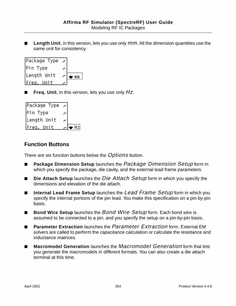
Affirma RF Simulator (SpectreRF) User GuideModeling RF IC Packages
Length Unit , in this version, lets you use only mm. All the dimension quantities use thesame unit for consistency.
Freq. Unit , in this version, lets you use only Hz.
Function Buttons
There are six function buttons below the Options button.
Package Dimension Setup launches the Package Dimension Setup form inwhich you specify the package, die cavity, and the external lead frame parameters.
Die Attach Setup launches the Die Attach Setup form in which you specify thedimensions and elevation of the die attach.
Internal Lead Frame Setup launches the Lead Frame Setup form in which youspecify the internal portions of the pin lead. You make this specification on a pin-by-pinbasis.
Bond Wire Setup launches the Bond Wire Setup form. Each bond wire isassumed to be connected to a pin, and you specify the setup on a pin-by-pin basis.
Parameter Extraction launches the Parameter Extraction form. External EMsolvers are called to perform the capacitance calculation or calculate the resistance andinductance matrices.
Macromodel Generation launches the Macromodel Generation form that letsyou generate the macromodels in different formats. You can also create a die attachterminal at this time.
April 2001 354 Product Version 4.4.6
Affirma RF Simulator (SpectreRF) User GuideModeling RF IC Packages
Package Dimension Setup
QFP Packages
The layout of the Package Dimension Setup form for QFP packages is shown inFigure 8-2 , in which a 48 pin rectangular QFP is displayed. The left portion of the displaycontains the data entries; the upper right portion of the display is the top view of the package;and the lower right portion is the side view of the package. Most data entries are illustrated inthe display, which changes interactively with the entry data.
April 2001 355 Product Version 4.4.6
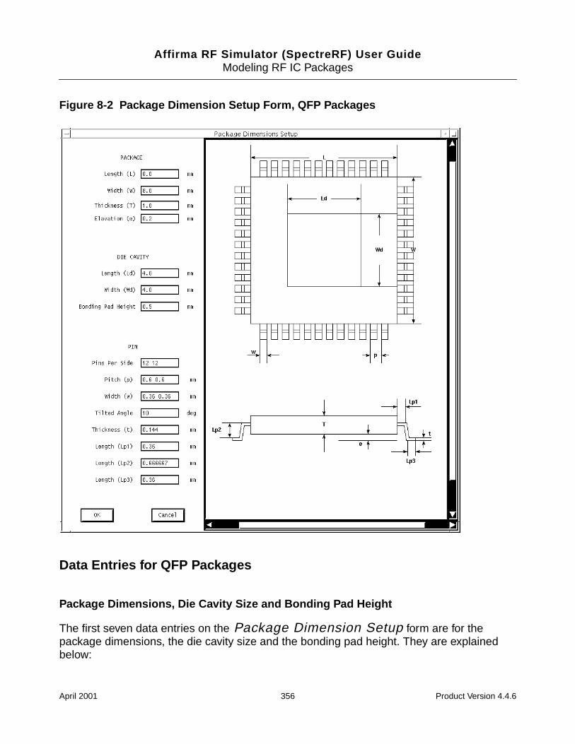
Affirma RF Simulator (SpectreRF) User GuideModeling RF IC Packages
Figure 8-2 Package Dimension Setup Form, QFP Packages
Data Entries for QFP Packages
Package Dimensions, Die Cavity Size and Bonding Pad Height
The first seven data entries on the Package Dimension Setup form are for thepackage dimensions, the die cavity size and the bonding pad height. They are explainedbelow:
April 2001 356 Product Version 4.4.6
Affirma RF Simulator (SpectreRF) User GuideModeling RF IC Packages
Length (L) : Length of the package body.
Width (W) : Width of the package body.
Thickness (T) : Thickness of the package body.
Elevation (e) : Distance from the bottom face of the package body to the lower horizontalpin segment.
Length (Ld) : Length of the die cavity formed by the leadframe. The cavity is assumedto be located in the center of the package body.
Width (Wd) : Width of the die cavity formed by the leadframe.
Bonding Pad Height : Height of the upper face of the die, where the bonding pads arelocated. The reference height 0 is the bottom face of the package body. This height canbe different from the height of the bond pad site on the pin, or on the die attach.
Lead Frame Dimensions
There are eight data entries on the Package Dimension Setup form for the lead framedimensions.
Pins per Side : For this entry, you specify one or two numbers. When you specify onenumber, all four sides have the same number of pins. If you specify two numbersseparated by space, the first number represents the number of pins on sides 1 and 3(bottom and top). The second number is the number of pins on sides 2 and 4 (left andright).
Pitch (P) : Distance between the left (or right) edges of two adjacent pins on the sameside. If you specify one number, the four sides have the same pin pitch. If you specify twonumbers, the first number is the pin pitch for the bottom and top sides, and the secondnumber is the pin pitch for the left and right sides.
Width (w) : Accepts one or two numbers in the same manner as Pitch (P). You canoverride this number by specifying values for individual pins.
Tilted Angle : Angle of pins measured from the vertical direction. Positive anglesrepresent outwardly tilted pins. Negative angles represent inwardly tilted pins.
Thickness (t) : Thickness of the pins. All the pins are assumed to have the samethickness.
Length (Lp1) : Length of the upper horizontal segment of the pins outside of thepackage body.
Length (Lp2): Length of the vertical segment of the pins.
April 2001 357 Product Version 4.4.6
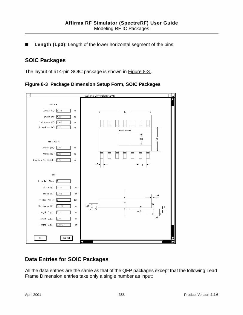
Affirma RF Simulator (SpectreRF) User GuideModeling RF IC Packages
Length (Lp3) : Length of the lower horizontal segment of the pins.
SOIC Packages
The layout of a14-pin SOIC package is shown in Figure 8-3 .
Figure 8-3 Package Dimension Setup Form, SOIC Packages
Data Entries for SOIC Packages
All the data entries are the same as that of the QFP packages except that the following LeadFrame Dimension entries take only a single number as input:
April 2001 358 Product Version 4.4.6
Affirma RF Simulator (SpectreRF) User GuideModeling RF IC Packages
Pins per Side : For this entry, you specify one number since both sides have the samenumber of pins.
Pitch (P) : Distance between the left (or right) edges of two adjacent pins on the sameside.
Width (w) : Accepts one number in the same manner as Pitch (P).
DIP Packages
The layout of the DIP package dimension setup is shown in Figure 8-4 . The data entry partand the side view part are different from those of the SOIC packages.
April 2001 359 Product Version 4.4.6
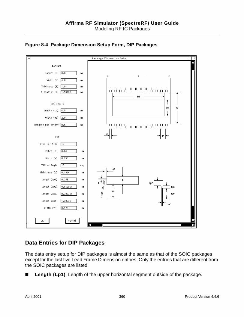
Affirma RF Simulator (SpectreRF) User GuideModeling RF IC Packages
Figure 8-4 Package Dimension Setup Form, DIP Packages
Data Entries for DIP Packages
The data entry setup for DIP packages is almost the same as that of the SOIC packagesexcept for the last five Lead Frame Dimension entries. Only the entries that are different fromthe SOIC packages are listed
Length (Lp1) : Length of the upper horizontal segment outside of the package.
April 2001 360 Product Version 4.4.6
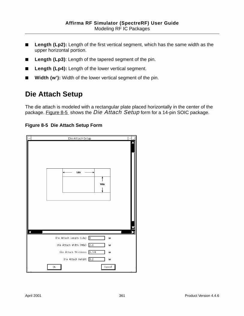
Affirma RF Simulator (SpectreRF) User GuideModeling RF IC Packages
Length (Lp2): Length of the first vertical segment, which has the same width as theupper horizontal portion.
Length (Lp3) : Length of the tapered segment of the pin.
Length (Lp4): Length of the lower vertical segment.
Width (w’): Width of the lower vertical segment of the pin.
Die Attach Setup
The die attach is modeled with a rectangular plate placed horizontally in the center of thepackage. Figure 8-5 shows the Die Attach Setup form for a 14-pin SOIC package.
Figure 8-5 Die Attach Setup Form
April 2001 361 Product Version 4.4.6
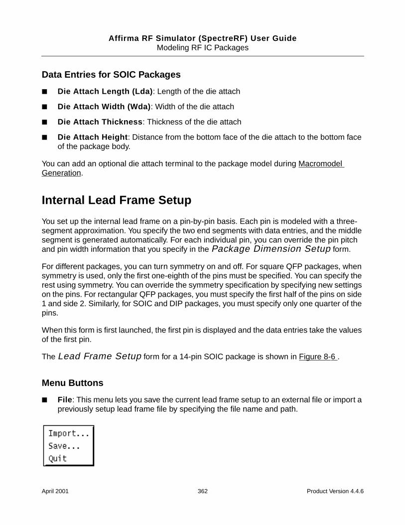
Affirma RF Simulator (SpectreRF) User GuideModeling RF IC Packages
Data Entries for SOIC Packages
Die Attach Length (Lda) : Length of the die attach
Die Attach Width (Wda) : Width of the die attach
Die Attach Thickness : Thickness of the die attach
Die Attach Height : Distance from the bottom face of the die attach to the bottom faceof the package body.
You can add an optional die attach terminal to the package model during MacromodelGeneration.
Internal Lead Frame Setup
You set up the internal lead frame on a pin-by-pin basis. Each pin is modeled with a three-segment approximation. You specify the two end segments with data entries, and the middlesegment is generated automatically. For each individual pin, you can override the pin pitchand pin width information that you specify in the Package Dimension Setup form.
For different packages, you can turn symmetry on and off. For square QFP packages, whensymmetry is used, only the first one-eighth of the pins must be specified. You can specify therest using symmetry. You can override the symmetry specification by specifying new settingson the pins. For rectangular QFP packages, you must specify the first half of the pins on side1 and side 2. Similarly, for SOIC and DIP packages, you must specify only one quarter of thepins.
When this form is first launched, the first pin is displayed and the data entries take the valuesof the first pin.
The Lead Frame Setup form for a 14-pin SOIC package is shown in Figure 8-6 .
Menu Buttons
File : This menu lets you save the current lead frame setup to an external file or import apreviously setup lead frame file by specifying the file name and path.
April 2001 362 Product Version 4.4.6

Affirma RF Simulator (SpectreRF) User GuideModeling RF IC Packages
Function Buttons
There are four function buttons just below the lead frame display that control the pin-by-pinsetup.
Previous : Switches to the previous pin (the current pin number minus one. If the currentpin is 1, then it switches to the last pin).
Accept : Accepts data entry values for the current pin. Without pushing this, the entryvalues do not take effect.
Undo : Cancel the specification and return to the initial values.
Next : Switch to the next pin (the current pin number plus 1). If the current pin is the lastpin, then switch to the first pin.
April 2001 363 Product Version 4.4.6
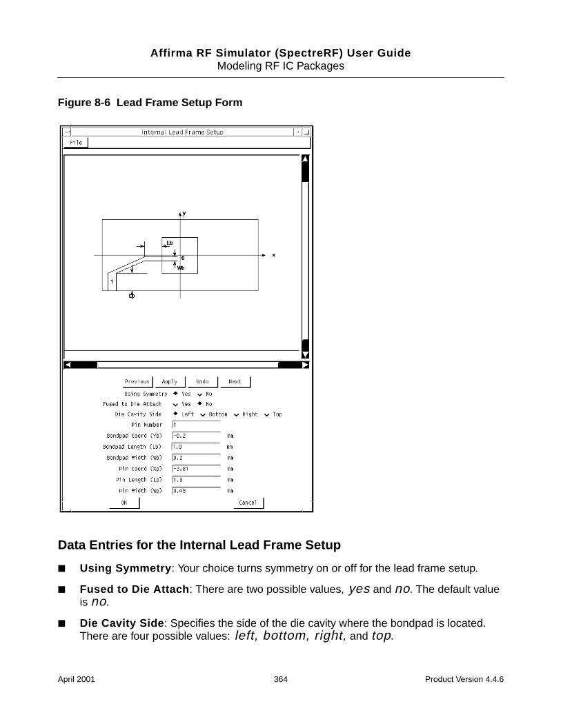
Affirma RF Simulator (SpectreRF) User GuideModeling RF IC Packages
Figure 8-6 Lead Frame Setup Form
Data Entries for the Internal Lead Frame Setup
Using Symmetry : Your choice turns symmetry on or off for the lead frame setup.
Fused to Die Attach : There are two possible values, yes and no. The default valueis no.
Die Cavity Side : Specifies the side of the die cavity where the bondpad is located.There are four possible values: left, bottom, right, and top.
April 2001 364 Product Version 4.4.6

Affirma RF Simulator (SpectreRF) User GuideModeling RF IC Packages
Pin Number : The pin number of the current pin. This number increases or decreaseswhen you push the Next or Previous buttons. You can specify the pin number directlyto change to that specific pin.
Bondpad Coord (Yb) : If the bondpad is on the bottom or top side of the die cavity, thenBondpad Coord is the x-coordinate of the center of the bondpad. If the bondpad ison the left or right side of the die cavity, then Bondpad Coord is the y-coordinate ofthe center of the bondpad. The origin of the coordinate system is the center of the diecavity.
Bondpad Length (Lb) : Length of the end segment of the pin with bond wiresconnecting to it.
Bondpad Width (Wb) : Width of the end segment of the pin with bond wires connectingto it.
Pin Coord (Xp) : If the pin is on the bottom or top side of the package body, then PinCoord is the x-coordinate of the center of the pin. If the pin is located at the left or rightside of the package, then Pin Coord is the y-coordinate of the center of the pin. Bychanging this number, you move the location of the pin.
Length (Lp) : Length of the first segment of the pin inside the package.
Pin Width (Wp) : Width of the current pin. Changing this number changes the width ofthe current pin only.
OK : Accepts all the changes you have made and exits from the Lead Frame Setupform.
Cancel : Cancels all the changes you have made and returns to the original values.
More about Using Symmetry
When you choose symmetry and the internal lead frame is symmetric, you need specify onlya quarter of the pins for SOIC, DIP, or rectangular QFP packages. For square QFP packages,you need specify only one-eighth of the pins.
Lead Frame File Format
You can write the internal lead frame into a file, or you can import a lead frame file thatcontains a lead frame you created externally. This feature allows you to manually edit the leadframe file without using the GUI or to get the lead frame from a layout library using a translator.The default location of the lead frame file is the current project directory. Because thedefinition of each pin depends on the package body and the die cavity dimensions, you mustset those parameters correctly before you import an external lead frame file.
April 2001 365 Product Version 4.4.6
Affirma RF Simulator (SpectreRF) User GuideModeling RF IC Packages
In the lead frame file, each pin is described with two array elements, pinPad(i) andbondPad(i) . Each element contains the length, width, location of the two end segments ofthe pin. The pinPad(i) array element has the following format:
pinPad(i) = package_side Xp(Yp) pin_widthpin_segment_length pin_number pin_fuse_to_da
bondPad(i) = bondpad_side Xb(Yb) bondpad_widthbondpad_length
The leadframe file of a 14-pin SOIC package is as follows:
bondPad(1) = left -0.2 0.2 1.0 0
pinPad(1) = bottom -3.81 0.49 1.0 1 0
bondPad(2) = left -0.6 0.2 0.49
pinPad(2) = bottom -2.54 0.49 1.0 2 0
bondPad(3) = bottom -0.6 0.2 0.2
pinPad(3) = bottom -1.27 0.49 0.2 3 0
bondPad(4) = bottom -0.0 0.2 0.2
pinPad(4) = bottom 0.0 0.49 0.2 4 0
bondPad(5) = bottom 0.6 0.2 0.2
pinPad(5) = bottom 1.27 0.49 0.2 5 0
bondPad(6) = right -0.6 0.2 0.49
pinPad(6) = bottom 2.54 0.49 1.0 6 0
bondPad(7) = right -0.2 0.2 1.0
pinPad(7) = bottom 3.81 0.49 1.0 7 0
bondPad(8) = right 0.2 0.2 1.0
pinPad(8) = top 3.81 0.49 1.0 8 0
bondPad(9) = right 0.6 0.2 0.49
pinPad(9) = top 2.54 0.49 1.0 9
bondPad(10) = top 0.6 0.2 0.2
pinPad(10) = top 1.27 0.49 0.2 10 0
bondPad(11) = top 0.0 0.2 0.2
pinPad(11) = top 0.0 0.49 0.2 11 0
bondPad(12) = top -0.6 0.2 0.2
pinPad(12) = top -1.27 0.49 0.2 12 0
bondPad(13) = left 0.6 0.2 0.49
pinPad(13) = top -2.54 0.49 1.0 13 0
bondPad(14) = left 0.2 0.2 1.0
pinPad(14) = top -3.81 0.49 1.0 14 0
April 2001 366 Product Version 4.4.6
Affirma RF Simulator (SpectreRF) User GuideModeling RF IC Packages
Bond Wire Setup
Like the lead frame, you set up the bond wires individually. Each bond wire is determined byits two end points, its length, its shape configuration, and its diameter. For the current version,only round bond wires are permitted. There are two different bond wire shape configurations,the quadratic and the exponential-distribution-like shape. There are three bondwireconnections. They are pin-to-die, pin-to-da, and die-to-da connection.
The layout of the Bond Wire Setup form is shown in Figure 8-7 .
Menu Buttons
There are two menu buttons on the top of the form.
File : This button lets you import and export bond wire data. Unless specified otherwise,the default location of the bond wire file is under the project directory. There is adifference between importing a bond wire file and a lead frame file. The new bond wirevalues do not take effect unless you push the OK button.
Options : In the current version, there is only one variable under this button, ShapeFunction, which is a radio button with two values, Quadratic and cx^a*EXP(-bx), which describe the shape of the bond wires.
Function Buttons
Under the display portion, there are five function buttons that are similar to the buttons in theLead Frame Setup form. These buttons control setup of individual bond wires. There aretwo function buttons at the bottom of the form that let you accept the setup and exit or cancelthe changes and exit.
April 2001 367 Product Version 4.4.6
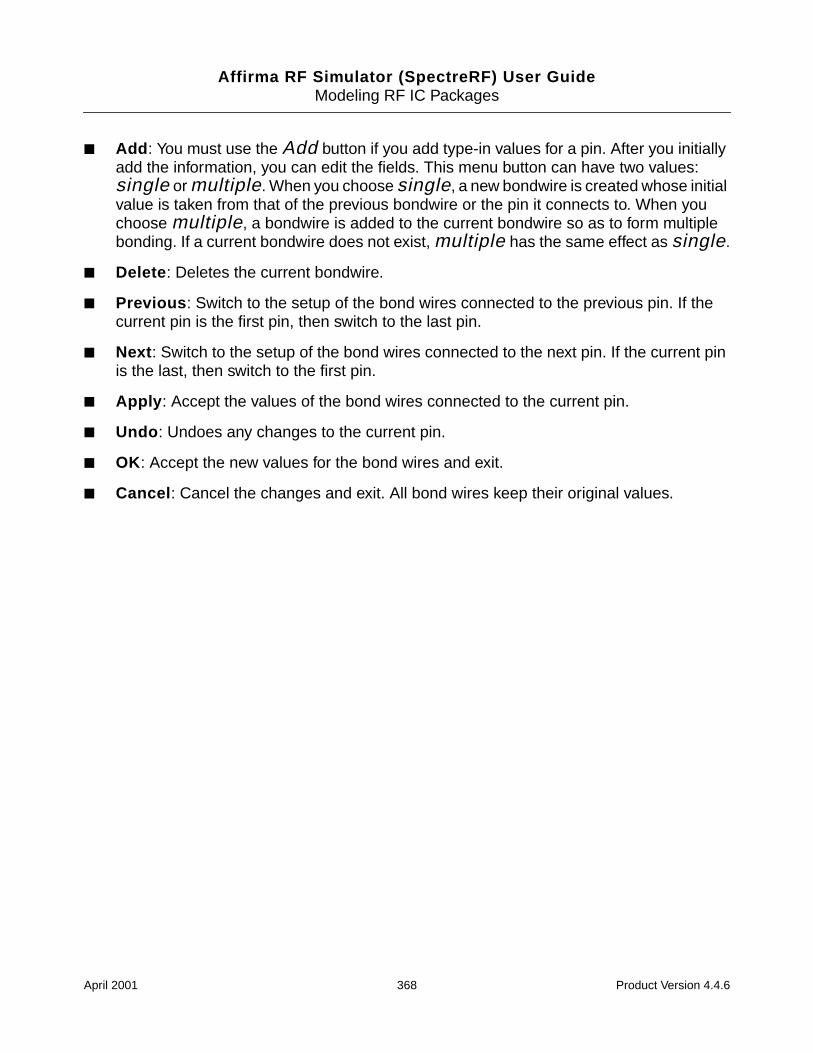
Affirma RF Simulator (SpectreRF) User GuideModeling RF IC Packages
Add : You must use the Add button if you add type-in values for a pin. After you initiallyadd the information, you can edit the fields. This menu button can have two values:single or multiple. When you choose single, a new bondwire is created whose initialvalue is taken from that of the previous bondwire or the pin it connects to. When youchoose multiple, a bondwire is added to the current bondwire so as to form multiplebonding. If a current bondwire does not exist, multiple has the same effect as single.
Delete : Deletes the current bondwire.
Previous : Switch to the setup of the bond wires connected to the previous pin. If thecurrent pin is the first pin, then switch to the last pin.
Next : Switch to the setup of the bond wires connected to the next pin. If the current pinis the last, then switch to the first pin.
Apply : Accept the values of the bond wires connected to the current pin.
Undo : Undoes any changes to the current pin.
OK : Accept the new values for the bond wires and exit.
Cancel : Cancel the changes and exit. All bond wires keep their original values.
April 2001 368 Product Version 4.4.6
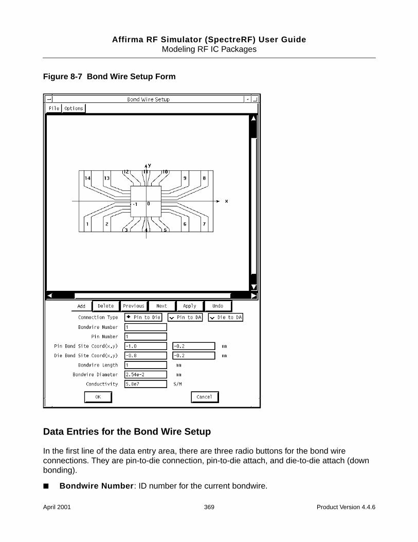
Affirma RF Simulator (SpectreRF) User GuideModeling RF IC Packages
Figure 8-7 Bond Wire Setup Form
Data Entries for the Bond Wire Setup
In the first line of the data entry area, there are three radio buttons for the bond wireconnections. They are pin-to-die connection, pin-to-die attach, and die-to-die attach (downbonding).
Bondwire Number : ID number for the current bondwire.
April 2001 369 Product Version 4.4.6

Affirma RF Simulator (SpectreRF) User GuideModeling RF IC Packages
Pin Number : Current pin number to which the bond wires are attached.
Pin Bond Site Coord (x, y) : Coordinates of the bond pad on the pin.
Die Bond Site Coord (x, y) : Coordinates of the bond pads on the die. The referenceorigin of the local coordinate system is the center of the die cavity.
Bondwire Length : Length of the bond wire(s). Given the coordinates of the bond pads,the length must be big enough; otherwise, an error condition occurs.
Bondwire Diameter : Diameter of the bond wires.
Conductivity : Conductivity of the bond wires. The default metal for conductivity is gold,which is The unit is S/m.
Bond Wire Configurations
PKG supports two configurations of bond wires. One configuration is defined by the quadraticfunction, the other is defined by an exponential-distribution-like function. For the two shapefunctions, the three unknown parameters a, b, and c are determined from the two end pointsand the length of the bond wire
Quadratic function (y=ax^2 +bx+c)
Figure 8-8 Quadratic Shape Function
April 2001 370 Product Version 4.4.6

Affirma RF Simulator (SpectreRF) User GuideModeling RF IC Packages
Exponential distribution cx a*Exp(-bx)
Figure 8-9 Exponential-Distribution-Like Shape Function
Bond Wire File Format
PKG lets you save the current bond wire setup to an external file and also import the datafrom an external source, such as a file from a database, or a file edited by hand. The file mustconform to the proper the format. The format and a sample bond wire data file are shownbelow.
bw(i) = pin_number connection_type x_coord y_coord z_coordpin_bondpad_displacement bondwire_lengthbondwire_conductivity
There are three possible values for the connection type: pin2die , pin2da , and die2die .
When the connection type is pin2die , x1 and y1 are the coordinates of the bonding site onthe end of the pin, x2 and y2 are the coordinates of the bonding site on the die. The die padnumber is the index number of the pad the bondwire connects to.
When the connection type is pin2da , x1 and y1 are the coordinates of the bonding site onthe end of the pin, and x2 and y2 are the coordinates of the bonding site on the die attachbecause the bonding wire does not connect to the die. The die pad number is -1.
When the connection type is die2die , x1 and y1 are the coordinates of the bonding site onthe die, x2 nd y2 are the bonding site coordinates on the die attach. The die pad number isthe index number of the pin on the die. Because the bondwire does not connect to a pin, thedie pad number is -1.
numBondwires = 14
bw(1) = 1 pin2die -1.0 -0.2 -0.8 -0.2 1 2.54e-2 5.8e7 1
bw(2) = 2 pin2die -1.0 -0.6 -0.8 -0.6 1 2.54e-2 5.8e7 2
bw(3) = 3 pin2die -0.6 -1.0 -0.6 -0.8 1 2.54e-2 5.8e7 3
April 2001 371 Product Version 4.4.6
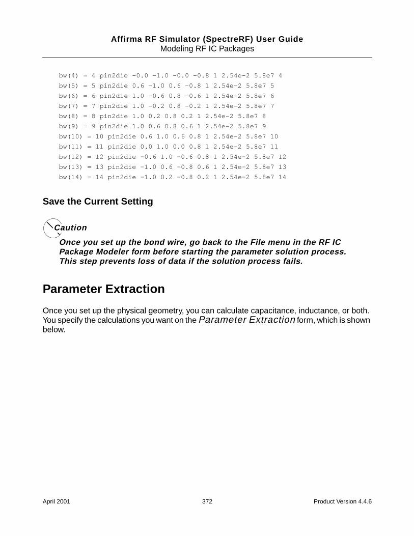
Affirma RF Simulator (SpectreRF) User GuideModeling RF IC Packages
bw(4) = 4 pin2die -0.0 -1.0 -0.0 -0.8 1 2.54e-2 5.8e7 4
bw(5) = 5 pin2die 0.6 -1.0 0.6 -0.8 1 2.54e-2 5.8e7 5
bw(6) = 6 pin2die 1.0 -0.6 0.8 -0.6 1 2.54e-2 5.8e7 6
bw(7) = 7 pin2die 1.0 -0.2 0.8 -0.2 1 2.54e-2 5.8e7 7
bw(8) = 8 pin2die 1.0 0.2 0.8 0.2 1 2.54e-2 5.8e7 8
bw(9) = 9 pin2die 1.0 0.6 0.8 0.6 1 2.54e-2 5.8e7 9
bw(10) = 10 pin2die 0.6 1.0 0.6 0.8 1 2.54e-2 5.8e7 10
bw(11) = 11 pin2die 0.0 1.0 0.0 0.8 1 2.54e-2 5.8e7 11
bw(12) = 12 pin2die -0.6 1.0 -0.6 0.8 1 2.54e-2 5.8e7 12
bw(13) = 13 pin2die -1.0 0.6 -0.8 0.6 1 2.54e-2 5.8e7 13
bw(14) = 14 pin2die -1.0 0.2 -0.8 0.2 1 2.54e-2 5.8e7 14
Save the Current Setting
Caution
Once you set up the bond wire, go back to the File menu in the RF ICPackage Modeler form before starting the parameter solution process.This step prevents loss of data if the solution process fails.
Parameter Extraction
Once you set up the physical geometry, you can calculate capacitance, inductance, or both.You specify the calculations you want on the Parameter Extraction form, which is shownbelow.
April 2001 372 Product Version 4.4.6
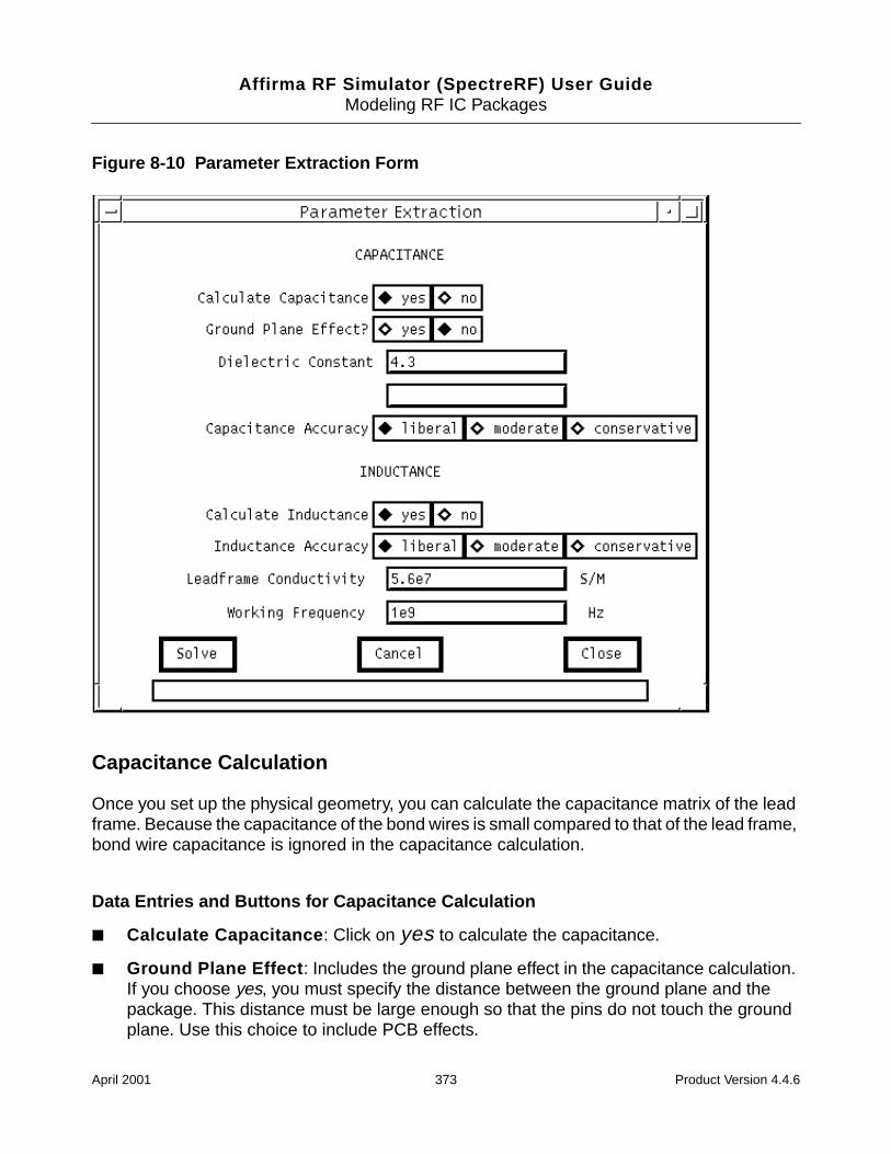
Affirma RF Simulator (SpectreRF) User GuideModeling RF IC Packages
Figure 8-10 Parameter Extraction Form
Capacitance Calculation
Once you set up the physical geometry, you can calculate the capacitance matrix of the leadframe. Because the capacitance of the bond wires is small compared to that of the lead frame,bond wire capacitance is ignored in the capacitance calculation.
Data Entries and Buttons for Capacitance Calculation
Calculate Capacitance : Click on yes to calculate the capacitance.
Ground Plane Effect : Includes the ground plane effect in the capacitance calculation.If you choose yes, you must specify the distance between the ground plane and thepackage. This distance must be large enough so that the pins do not touch the groundplane. Use this choice to include PCB effects.
April 2001 373 Product Version 4.4.6
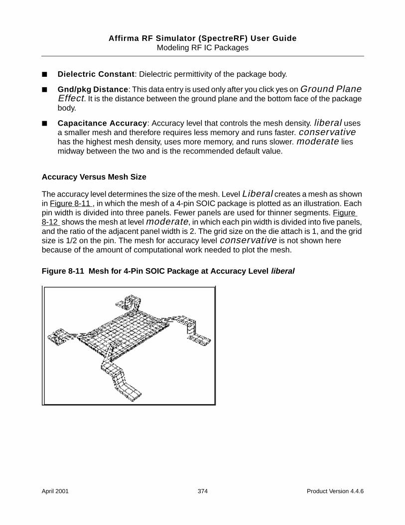
Affirma RF Simulator (SpectreRF) User GuideModeling RF IC Packages
Dielectric Constant : Dielectric permittivity of the package body.
Gnd/pkg Distance : This data entry is used only after you click yes on Ground PlaneEffect. It is the distance between the ground plane and the bottom face of the packagebody.
Capacitance Accuracy : Accuracy level that controls the mesh density. liberal usesa smaller mesh and therefore requires less memory and runs faster. conservativehas the highest mesh density, uses more memory, and runs slower. moderate liesmidway between the two and is the recommended default value.
Accuracy Versus Mesh Size
The accuracy level determines the size of the mesh. Level Liberal creates a mesh as shownin Figure 8-11 , in which the mesh of a 4-pin SOIC package is plotted as an illustration. Eachpin width is divided into three panels. Fewer panels are used for thinner segments. Figure8-12 shows the mesh at level moderate, in which each pin width is divided into five panels,and the ratio of the adjacent panel width is 2. The grid size on the die attach is 1, and the gridsize is 1/2 on the pin. The mesh for accuracy level conservative is not shown herebecause of the amount of computational work needed to plot the mesh.
Figure 8-11 Mesh for 4-Pin SOIC Package at Accuracy Level liberal
April 2001 374 Product Version 4.4.6
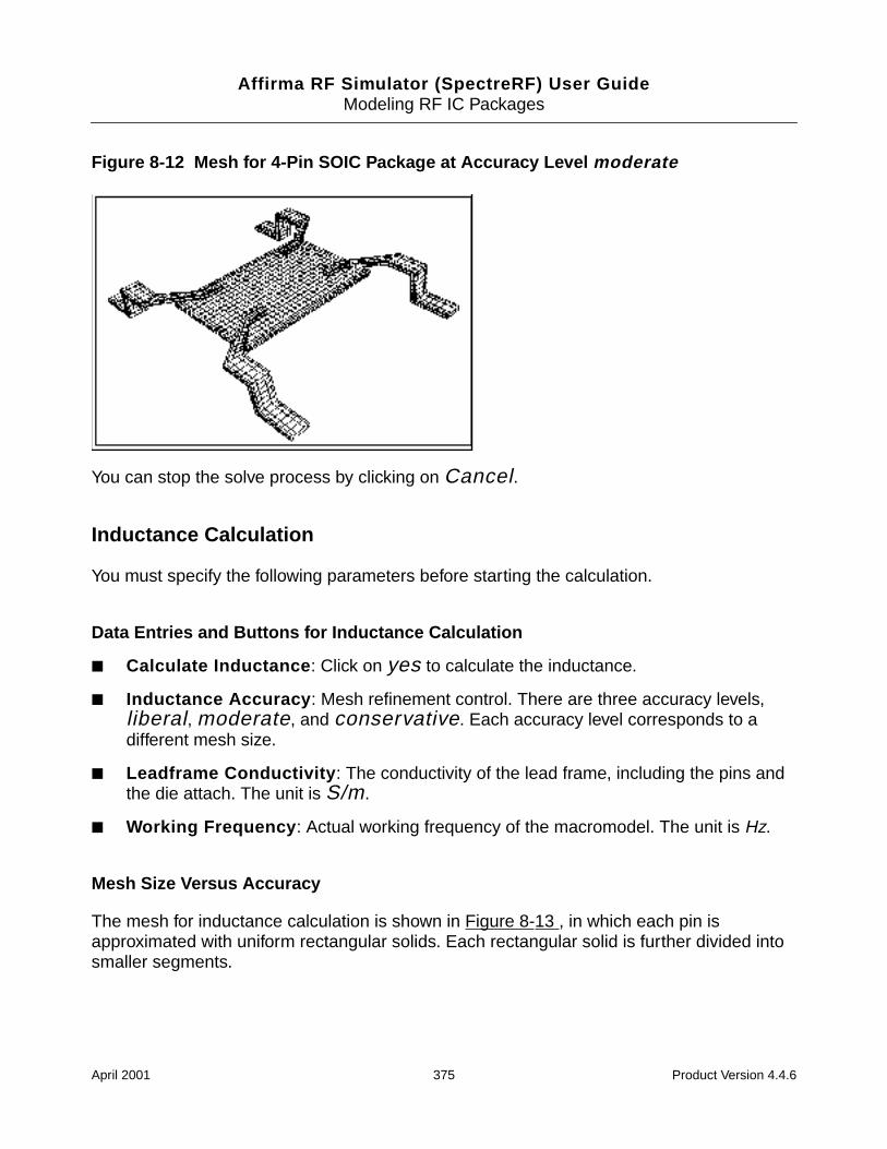
Affirma RF Simulator (SpectreRF) User GuideModeling RF IC Packages
Figure 8-12 Mesh for 4-Pin SOIC Package at Accuracy Level moderate
You can stop the solve process by clicking on Cancel.
Inductance Calculation
You must specify the following parameters before starting the calculation.
Data Entries and Buttons for Inductance Calculation
Calculate Inductance : Click on yes to calculate the inductance.
Inductance Accuracy : Mesh refinement control. There are three accuracy levels,liberal, moderate, and conservative. Each accuracy level corresponds to adifferent mesh size.
Leadframe Conductivity : The conductivity of the lead frame, including the pins andthe die attach. The unit is S/m.
Working Frequency : Actual working frequency of the macromodel. The unit is Hz.
Mesh Size Versus Accuracy
The mesh for inductance calculation is shown in Figure 8-13 , in which each pin isapproximated with uniform rectangular solids. Each rectangular solid is further divided intosmaller segments.
April 2001 375 Product Version 4.4.6
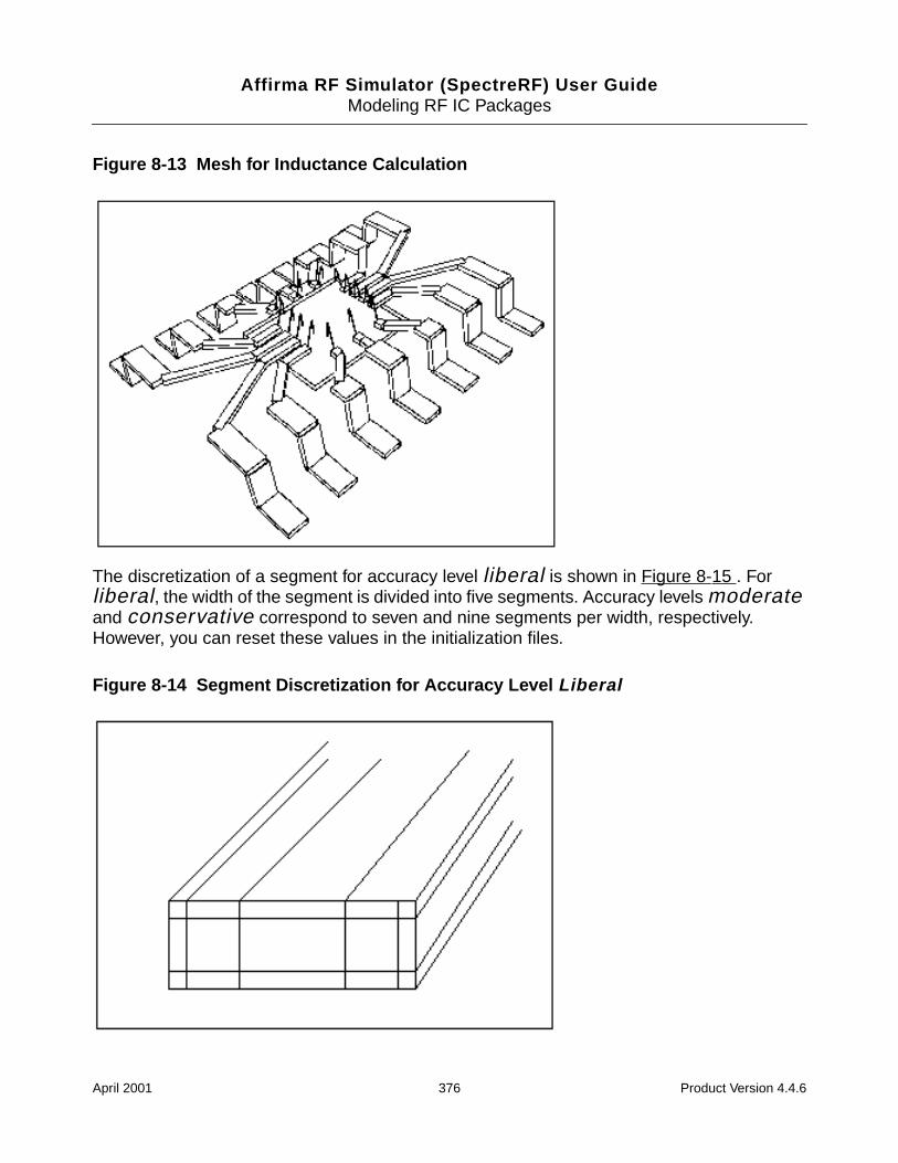
Affirma RF Simulator (SpectreRF) User GuideModeling RF IC Packages
Figure 8-13 Mesh for Inductance Calculation
The discretization of a segment for accuracy level liberal is shown in Figure 8-15 . Forliberal, the width of the segment is divided into five segments. Accuracy levels moderateand conservative correspond to seven and nine segments per width, respectively.However, you can reset these values in the initialization files.
Figure 8-14 Segment Discretization for Accuracy Level Liberal
April 2001 376 Product Version 4.4.6
Affirma RF Simulator (SpectreRF) User GuideModeling RF IC Packages
The Inductance Solving Process
Because of the skin-depth effect, the electric current crowds out to the surface as thefrequency increases. Consequently, you must generate a very fine mesh to catch the fastvariation of current distribution in the vicinity of the surface. However, this large mesh makesthe solving process very slow, or in some cases, impossible.
PKG employs a two-step solving process. The first step is to calculate the whole package atthe corner frequency. Because the electric current is nearly uniform, a small mesh of a coupleof segments per width is sufficient. This makes the solving process very fast. Because themutual inductances between pins and vias do not change much when the frequencyincreases, the mutual inductance calculated at the low frequency can be used for the muchhigher working frequency. In the second step, to account for the skin depth effect, each pin(plus the bond wire, if present) is solved independently with a finer mesh at the workingfrequency. The impedance matrix at the working frequency can be obtained by combining thetwo sets of results.
Function Buttons for Parameter Extraction
There are three buttons at the bottom of the Parameter Extraction form. They are Solve,Cancel, and Close.
Solve starts the parameter extraction calculations. Capacitance is calculated first, theninductance. If the capacitance or inductance has already been calculated, a warningmessage appears.
Cancel stops the parameter extraction calculations.
Close closes the parameter extraction form.
Macromodel Generation
After the parameter extraction has completed, you can generate the macromodel by pushingthe Macromodel Generation button on the RF IC Package Modeler form.Pushing the button brings up the Macromodel Generation form shown in Figure 8-15 .Before you create the macromodel, you must specify the items described below:
Data Entries and Buttons for Macromodel Generation
Coupled Pins Per Side : Number of the most adjacent pins on each side of the currentpin. If you choose 0, the coupling between pins is ignored. If the number you specify is
April 2001 377 Product Version 4.4.6
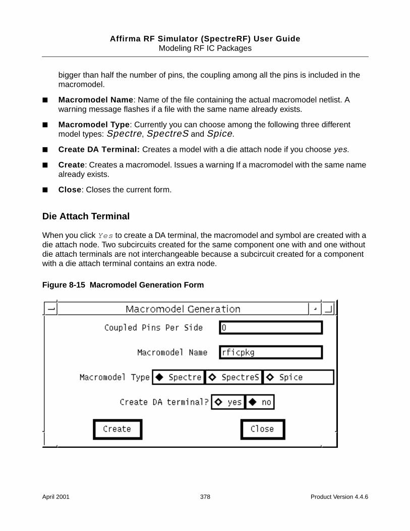
Affirma RF Simulator (SpectreRF) User GuideModeling RF IC Packages
bigger than half the number of pins, the coupling among all the pins is included in themacromodel.
Macromodel Name : Name of the file containing the actual macromodel netlist. Awarning message flashes if a file with the same name already exists.
Macromodel Type : Currently you can choose among the following three differentmodel types: Spectre, SpectreS and Spice.
Create DA Terminal: Creates a model with a die attach node if you choose yes.
Create : Creates a macromodel. Issues a warning If a macromodel with the same namealready exists.
Close : Closes the current form.
Die Attach Terminal
When you click Yes to create a DA terminal, the macromodel and symbol are created with adie attach node. Two subcircuits created for the same component one with and one withoutdie attach terminals are not interchangeable because a subcircuit created for a componentwith a die attach terminal contains an extra node.
Figure 8-15 Macromodel Generation Form
April 2001 378 Product Version 4.4.6
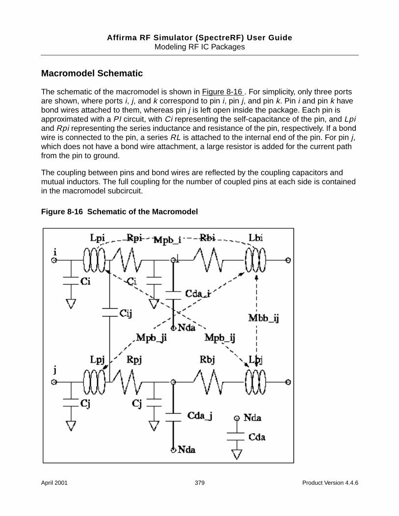
Affirma RF Simulator (SpectreRF) User GuideModeling RF IC Packages
Macromodel Schematic
The schematic of the macromodel is shown in Figure 8-16 . For simplicity, only three portsare shown, where ports i, j, and k correspond to pin i, pin j, and pin k. Pin i and pin k havebond wires attached to them, whereas pin j is left open inside the package. Each pin isapproximated with a PI circuit, with Ci representing the self-capacitance of the pin, and Lpiand Rpi representing the series inductance and resistance of the pin, respectively. If a bondwire is connected to the pin, a series RL is attached to the internal end of the pin. For pin j,which does not have a bond wire attachment, a large resistor is added for the current pathfrom the pin to ground.
The coupling between pins and bond wires are reflected by the coupling capacitors andmutual inductors. The full coupling for the number of coupled pins at each side is containedin the macromodel subcircuit.
Figure 8-16 Schematic of the Macromodel
April 2001 379 Product Version 4.4.6
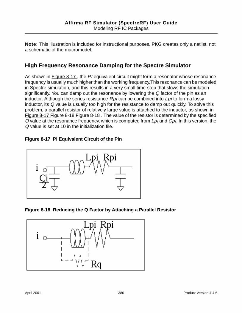
Affirma RF Simulator (SpectreRF) User GuideModeling RF IC Packages
Note: This illustration is included for instructional purposes. PKG creates only a netlist, nota schematic of the macromodel.
High Frequency Resonance Damping for the Spectre Simulator
As shown in Figure 8-17 , the PI equivalent circuit might form a resonator whose resonancefrequency is usually much higher than the working frequency.This resonance can be modeledin Spectre simulation, and this results in a very small time-step that slows the simulationsignificantly. You can damp out the resonance by lowering the Q factor of the pin as aninductor. Although the series resistance Rpi can be combined into Lpi to form a lossyinductor, its Q value is usually too high for the resistance to damp out quickly. To solve thisproblem, a parallel resistor of relatively large value is attached to the inductor, as shown inFigure 8-17 Figure 8-18 Figure 8-18 . The value of the resistor is determined by the specifiedQ value at the resonance frequency, which is computed from Lpi and Cpi. In this version, theQ value is set at 10 in the initialization file.
Figure 8-17 PI Equivalent Circuit of the Pin
Figure 8-18 Reducing the Q Factor by Attaching a Parallel Resistor
April 2001 380 Product Version 4.4.6

Affirma RF Simulator (SpectreRF) User GuideModeling RF IC Packages
Accuracy Analysis
One error source for the macromodel is the quasi-static assumption, in which the size of thepackage is assumed to be sufficiently small electrically so that the field retardation can beignored. This assumption determines the upper frequency limit. Therefore, the upperfrequency limit really depends upon which part of the package is of interest. If the long rangecoupling is of interest, then the upper frequency limit is lower because of the longer distancebetween the pins. If only the coupling between the neighboring pins is of interest, the upperfrequency limit can be higher due to the smaller distance between the pins.
The error with physical geometry mainly results from the three-segment approximation of thepins, the rectangular plate approximation of the die attach, and the ignoring of the bondingpad on the die, and so on. The error is mostly with the dimensions of the conductors, such aslength, thickness, and so on.
Another source of error is electrical modeling. For example, in inductance calculation, onlythe axial current is considered, and the transverse current is ignored. (Transverse current issmall at low frequencies.)
The error with capacitance calculation is small, usually under 1 percent.
The error with inductance calculation depends on the working frequency. Usually, error withinductance is very small. The error is relatively larger for resistance of the pins due to the skin-depth effect. However, the error has little effect on the accuracy of the result because of theattachment of a resistor that forces a decrease in the inductor Q factor.
Simulation of Package Models in the Affirma Analog Circuit DesignEnvironment
The symbol rfpkg and the Edit Object Properties form for the cell view are shown in Figure8-19 and Figure 8-20 . The left side of the symbol represents the terminals of the pin leadsoutside of the package. The ports on the right side of the symbol represent the bonding padson the die.
April 2001 381 Product Version 4.4.6
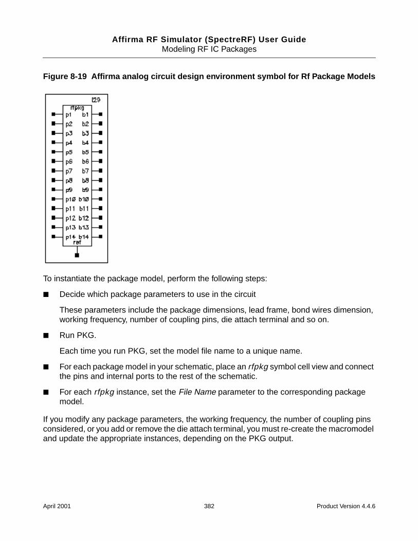
Affirma RF Simulator (SpectreRF) User GuideModeling RF IC Packages
Figure 8-19 Affirma analog circuit design environment symbol for Rf Package Models
To instantiate the package model, perform the following steps:
Decide which package parameters to use in the circuit
These parameters include the package dimensions, lead frame, bond wires dimension,working frequency, number of coupling pins, die attach terminal and so on.
Run PKG.
Each time you run PKG, set the model file name to a unique name.
For each package model in your schematic, place an rfpkg symbol cell view and connectthe pins and internal ports to the rest of the schematic.
For each rfpkg instance, set the File Name parameter to the corresponding packagemodel.
If you modify any package parameters, the working frequency, the number of coupling pinsconsidered, or you add or remove the die attach terminal, you must re-create the macromodeland update the appropriate instances, depending on the PKG output.
April 2001 382 Product Version 4.4.6
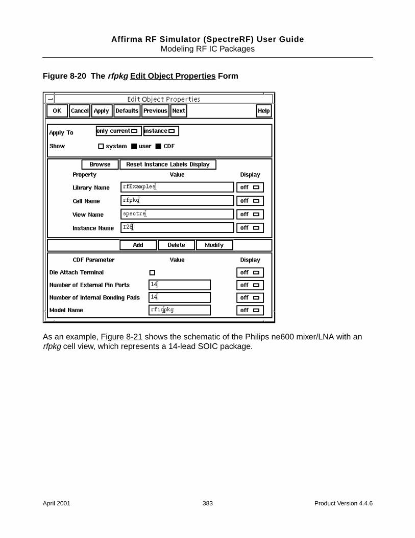
Affirma RF Simulator (SpectreRF) User GuideModeling RF IC Packages
Figure 8-20 The rfpkg Edit Object Pr oper ties Form
As an example, Figure 8-21 shows the schematic of the Philips ne600 mixer/LNA with anrfpkg cell view, which represents a 14-lead SOIC package.
April 2001 383 Product Version 4.4.6
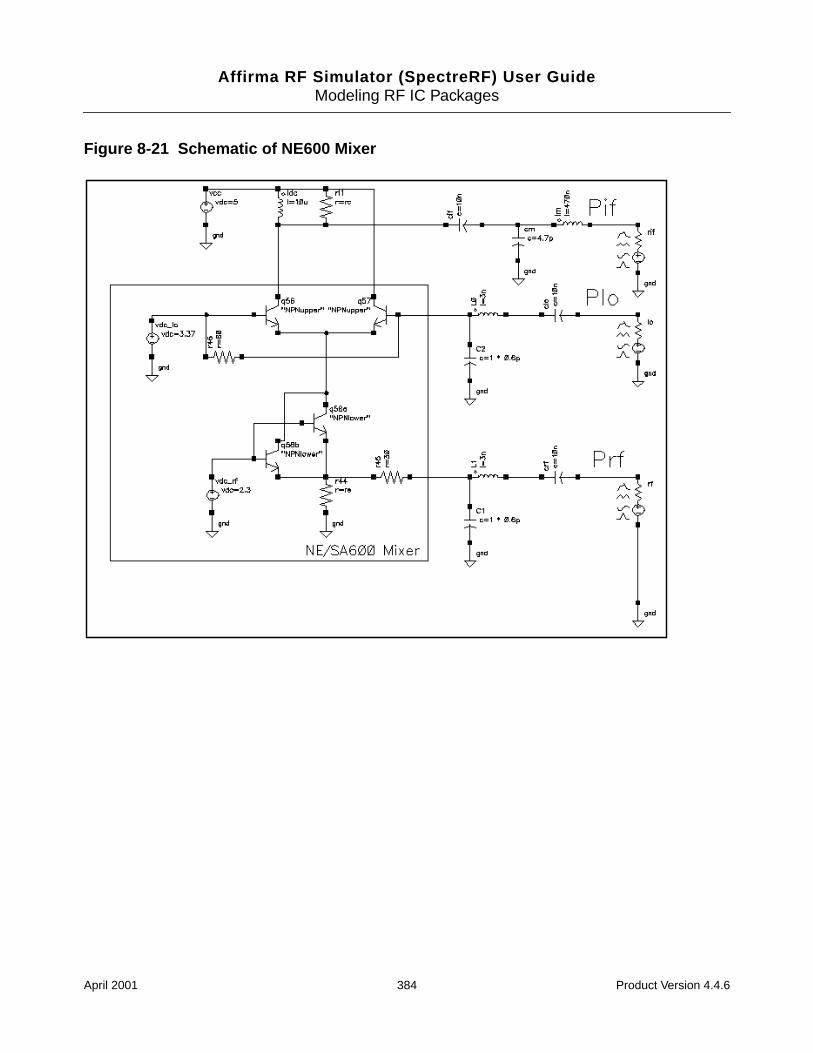
Affirma RF Simulator (SpectreRF) User GuideModeling RF IC Packages
Figure 8-21 Schematic of NE600 Mixer
April 2001 384 Product Version 4.4.6
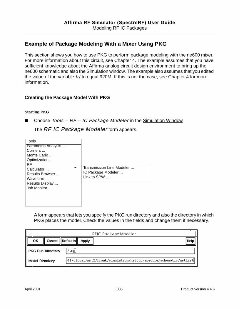
Affirma RF Simulator (SpectreRF) User GuideModeling RF IC Packages
Example of Package Modeling With a Mixer Using PKG
This section shows you how to use PKG to perform package modeling with the ne600 mixer.For more information about this circuit, see Chapter 4. The example assumes that you havesufficient knowledge about the Affirma analog circuit design environment to bring up thene600 schematic and also the Simulation window. The example also assumes that you editedthe value of the variable frf to equal 920M. If this is not the case, see Chapter 4 for moreinformation.
Creating the Package Model With PKG
Starting PKG
Choose Tools – RF – IC Package Modeler in the Simulation Window.
The RF IC Package Modeler form appears.
A form appears that lets you specify the PKG run directory and also the directory in whichPKG places the model. Check the values in the fields and change them if necessary.
ToolsParametric Analysis ...Corners ...Monte Carlo ...Optimization...RFCalculator ...Results Browser ...Waveform ...Results Display ...Job Monitor ...
Transmission Line Modeler ...IC Package Modeler ...Link to SPW ... .
April 2001 385 Product Version 4.4.6
Affirma RF Simulator (SpectreRF) User GuideModeling RF IC Packages
Click OK or Apply to approve the values in the PKG Run Directory and ModelDirectory fields.
The RF IC Package Modeler form appears.
Filling in the RF IC Package Modeler Form
In the RF IC Package Modeler form, perform the following:
1. Choose Options – Package Type – SOIC.
2. Choose Options – Pin Type – Gull-Wing.
April 2001 386 Product Version 4.4.6
Affirma RF Simulator (SpectreRF) User GuideModeling RF IC Packages
The diagram on the RF IC Package Modeler form changes to reflect yourmodifications. When you edit subsequent forms, the diagram on the RF IC PackageModeler form is updated to reflect these changes also.
3. Click on Package Dimensions Setup.
April 2001 387 Product Version 4.4.6
Affirma RF Simulator (SpectreRF) User GuideModeling RF IC Packages
The Package Dimensions Setup form appears.
Filling In the Package Dimensions Setup Form
1. In the Package Dimensions Setup form, type values as shown in the tablesbelow.
April 2001 388 Product Version 4.4.6
Affirma RF Simulator (SpectreRF) User GuideModeling RF IC Packages
As you type values, the pictures on the right side of the form change to reflect the valuesyou type.
Package Values Labels Values You Type
Length (L) 8.75
Width (W) 4.0
Thickness (T) 1.45
Elevation (e) 0.2
Die Cavity Labels Values You Type
Length (Ld) 2.0
Width (Wd) 2.0
Bonding Pad Height 0.5
Pin Labels Values You Type
Pins Per Side 7
Pitch (P) 1.27
Width (W) 0.49
Tilted Angle 8
Thickness (t) 0.127
Length (Lp1) 0.2
Length (Lp2) 0.8
Length (Lp3) 0.875
April 2001 389 Product Version 4.4.6
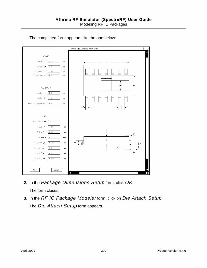
Affirma RF Simulator (SpectreRF) User GuideModeling RF IC Packages
The completed form appears like the one below:
2. In the Package Dimensions Setup form, click OK.
The form closes.
3. In the RF IC Package Modeler form, click on Die Attach Setup
The Die Attach Setup form appears.
April 2001 390 Product Version 4.4.6
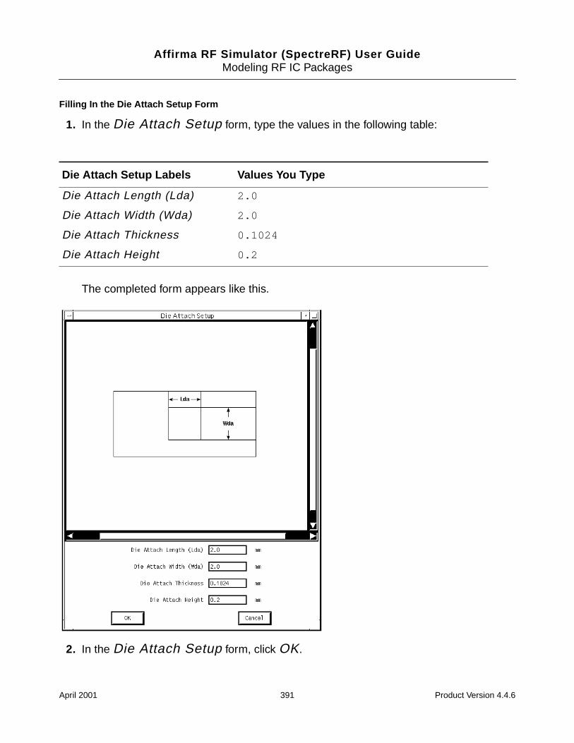
Affirma RF Simulator (SpectreRF) User GuideModeling RF IC Packages
Filling In the Die Attach Setup Form
1. In the Die Attach Setup form, type the values in the following table:
The completed form appears like this.
2. In the Die Attach Setup form, click OK.
Die Attach Setup Labels Values You Type
Die Attach Length (Lda) 2.0
Die Attach Width (Wda) 2.0
Die Attach Thickness 0.1024
Die Attach Height 0.2
April 2001 391 Product Version 4.4.6
Affirma RF Simulator (SpectreRF) User GuideModeling RF IC Packages
3. In the RF IC Package Modeler form, click on Internal Lead Frame Setup.
The Internal Lead Frame Setup form appears.
Filling-In the Internal Lead Frame Setup Form
In the Internal Lead Frame Setup form
1. Highlight yes for Using Symmetry.
2. Highlight no for Fused to Die Attach.
3. Specify the values in the following table.
4. Click on Apply.
Because you have chosen Using Symmetry, PKG places your settings on pins 7, 8,and 14, as well as pin 1. It duplicates your settings in all four quadrants each time youapply them.
5. Click on Next.
The form changes to let you specify values for pin 2.
Internal Lead Frame Setup Labels Values
Die Cavity Side Left
Pin Number 1
Bondpad Coord (Yb) -0.2
Bondpad Length (Lb) 1.0
Bondpad Width (Wb) 0.2
Pin Coord (Xp) -3.81
Pin Length (Lp) 1.0
Pin Width (Wp) 0.49
April 2001 392 Product Version 4.4.6
Affirma RF Simulator (SpectreRF) User GuideModeling RF IC Packages
6. Specify the values in the following table:
7. Click on Apply.
8. Click on Next.
The form changes to let you specify values for pin 3.
9. Specify the values in the following table:
10. Click on Apply.
Internal Lead Frame Setup Labels Values
Die Cavity Side Left
Pin Number 2
Bondpad Coord (Yb) -0.6
Bondpad Length (Lb) 0.49
Bondpad Width (Wb) 0.2
Pin Coord (Xp) -2.54
Pin Length (Lp) 1.0
Pin Width (Wp) 0.49
Internal Lead Frame Setup Labels Values
Die Cavity Side Bottom
Pin Number 3
Bondpad Coord (Yb) -0.6
Bondpad Length (Lb) 0.2
Bondpad Width (Wb) 0.49
Pin Coord (Xp) -1.27
Pin Length (Lp) 0.2
Pin Width (Wp) 0.49
April 2001 393 Product Version 4.4.6
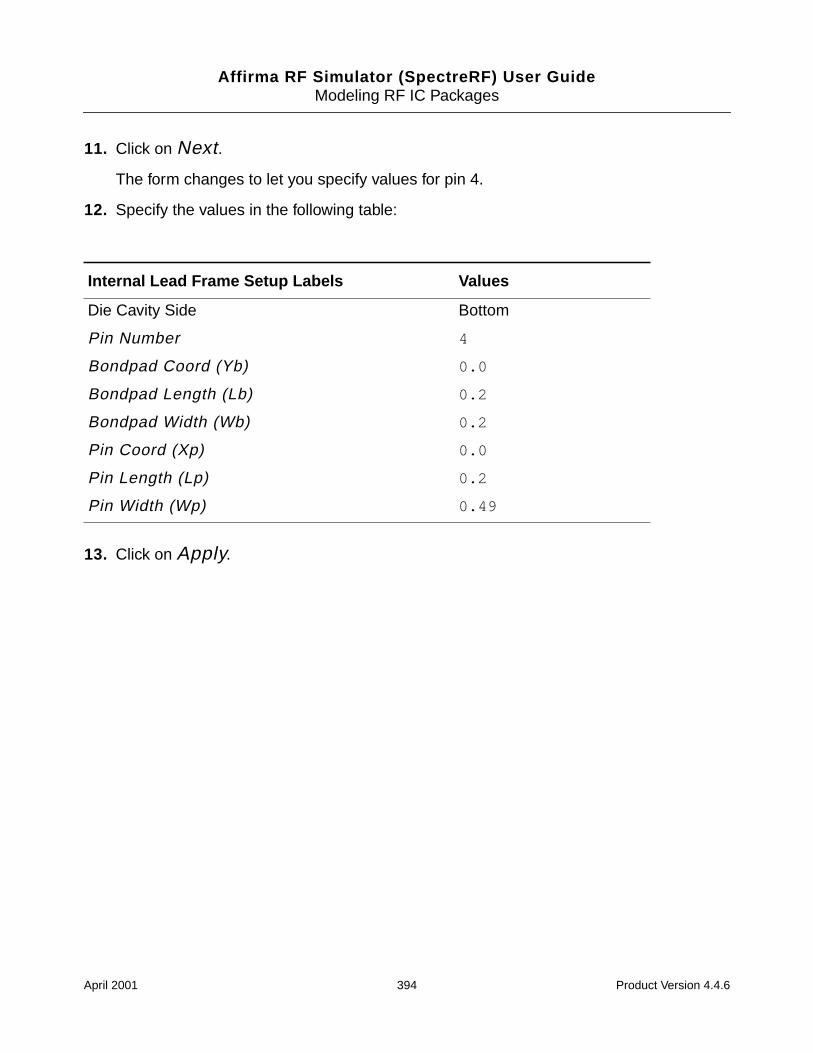
Affirma RF Simulator (SpectreRF) User GuideModeling RF IC Packages
11. Click on Next.
The form changes to let you specify values for pin 4.
12. Specify the values in the following table:
13. Click on Apply.
Internal Lead Frame Setup Labels Values
Die Cavity Side Bottom
Pin Number 4
Bondpad Coord (Yb) 0.0
Bondpad Length (Lb) 0.2
Bondpad Width (Wb) 0.2
Pin Coord (Xp) 0.0
Pin Length (Lp) 0.2
Pin Width (Wp) 0.49
April 2001 394 Product Version 4.4.6
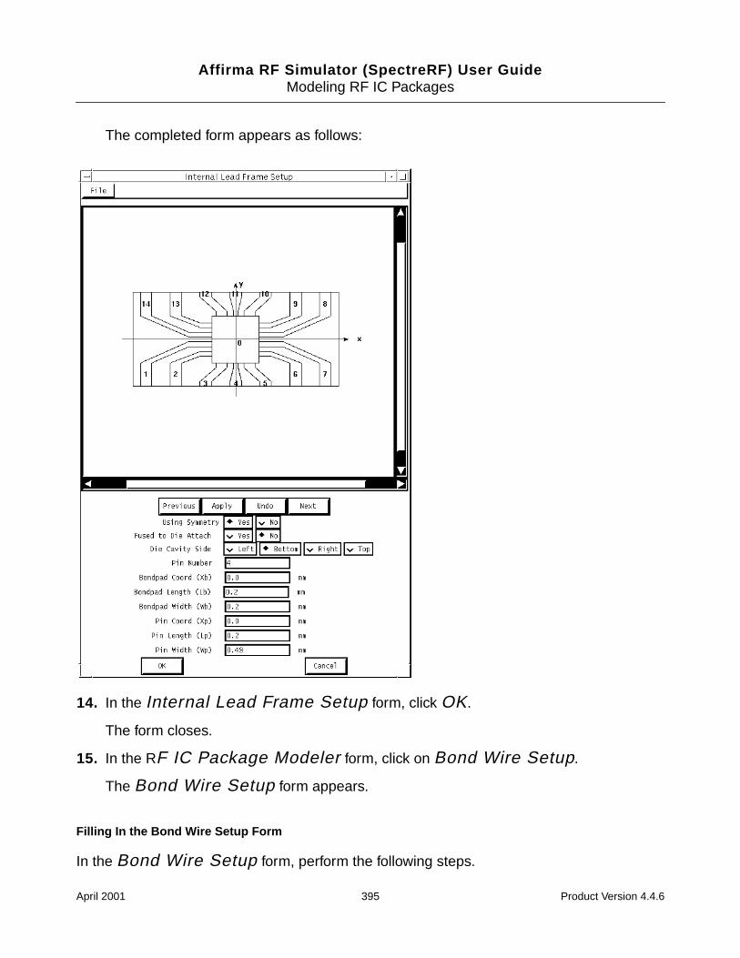
Affirma RF Simulator (SpectreRF) User GuideModeling RF IC Packages
The completed form appears as follows:
14. In the Internal Lead Frame Setup form, click OK.
The form closes.
15. In the RF IC Package Modeler form, click on Bond Wire Setup.
The Bond Wire Setup form appears.
Filling In the Bond Wire Setup Form
In the Bond Wire Setup form, perform the following steps.
April 2001 395 Product Version 4.4.6
Affirma RF Simulator (SpectreRF) User GuideModeling RF IC Packages
1. Highlight Pin to Die for the Connection Type.
2. Click on Add and choose Add – Single.
You must click on Add to place a bondwire. You can add either a single bondwire ormultiple bondwires. After you complete this step, you can specify values for the firstbondwire.
3. Edit the values in the form to the values in the following table:
4. Click on Apply.
You have completed specification for the first bondwire.
5. Repeat the sequence of steps “choose Add – Single followed by click on Apply” 13times, once for each remaining bondwire.
This example does not require any editing of the bondwire specifications after the firstbondwire, but you still must click on Apply for each bondwire to place each bondwire.The values you changed for the first bondwire remain as defaults for the followingspecifications. If you want to edit values for individual bondwires, you type the new valuesin the form before you click on Apply. After you perform the Add – Single operation,the number of the bondwire you are editing appears in the diagram in the BondwireSetup form. After you click on Apply, the numbers of all the bondwires you haveplaced appear in the same diagram.
Bond Wire Setup Labels Values You Type
Bondwire Number 1
Pin Number 1
Pin Bond Site Coord(x, y) -1.0 and -0.2
Die Bond Site Coord(x, y) -0.8 and -0.2
Bondwire Length 1
Bondwire Diameter 2.54e-2
Conductivity 5.8e7
April 2001 396 Product Version 4.4.6
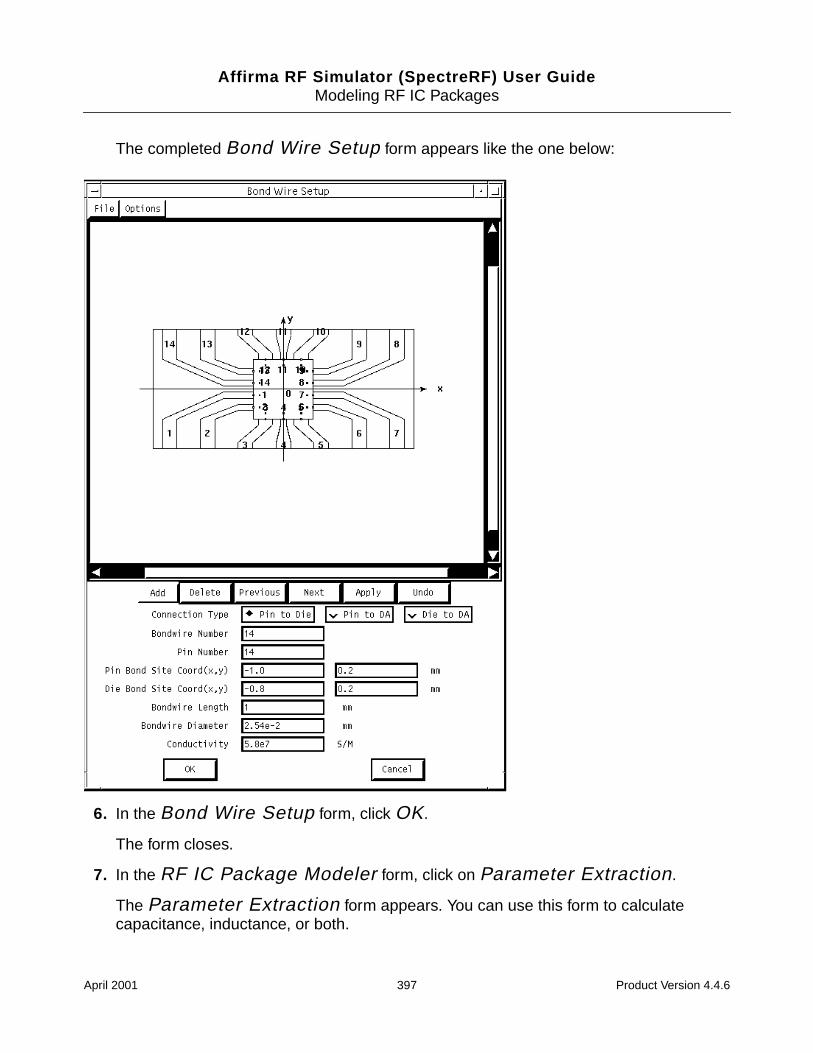
Affirma RF Simulator (SpectreRF) User GuideModeling RF IC Packages
The completed Bond Wire Setup form appears like the one below:
6. In the Bond Wire Setup form, click OK.
The form closes.
7. In the RF IC Package Modeler form, click on Parameter Extraction.
The Parameter Extraction form appears. You can use this form to calculatecapacitance, inductance, or both.
April 2001 397 Product Version 4.4.6
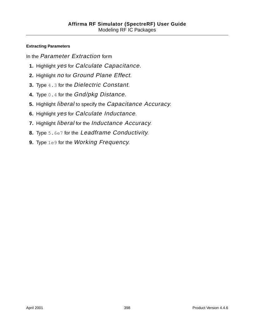
Affirma RF Simulator (SpectreRF) User GuideModeling RF IC Packages
Extracting Parameters
In the Parameter Extraction form
1. Highlight yes for Calculate Capacitance.
2. Highlight no for Ground Plane Effect.
3. Type 4.3 for the Dielectric Constant.
4. Type 0.4 for the Gnd/pkg Distance.
5. Highlight liberal to specify the Capacitance Accuracy.
6. Highlight yes for Calculate Inductance.
7. Highlight liberal for the Inductance Accuracy.
8. Type 5.6e7 for the Leadframe Conductivity.
9. Type 1e9 for the Working Frequency.
April 2001 398 Product Version 4.4.6
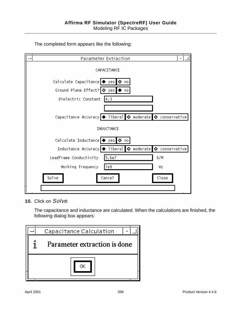
Affirma RF Simulator (SpectreRF) User GuideModeling RF IC Packages
The completed form appears like the following:
10. Click on Solve.
The capacitance and inductance are calculated. When the calculations are finished, thefollowing dialog box appears:
April 2001 399 Product Version 4.4.6
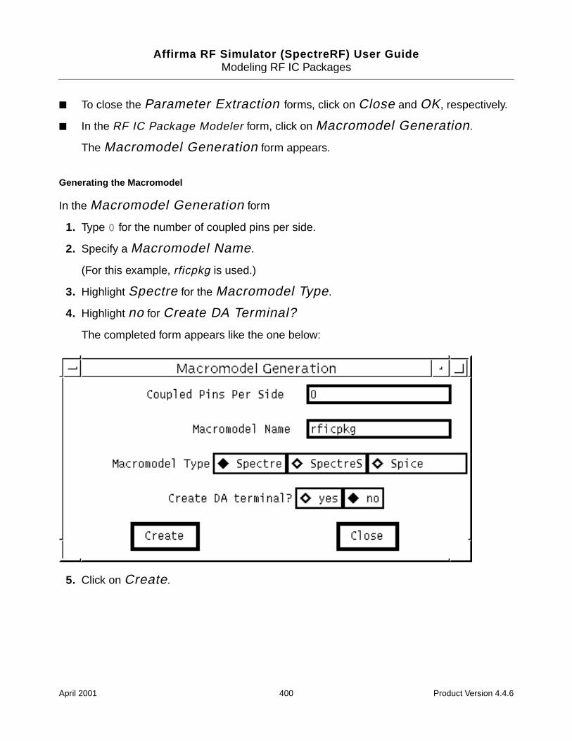
Affirma RF Simulator (SpectreRF) User GuideModeling RF IC Packages
To close the Parameter Extraction forms, click on Close and OK, respectively.
In the RF IC Package Modeler form, click on Macromodel Generation.
The Macromodel Generation form appears.
Generating the Macromodel
In the Macromodel Generation form
1. Type 0 for the number of coupled pins per side.
2. Specify a Macromodel Name.
(For this example, rficpkg is used.)
3. Highlight Spectre for the Macromodel Type.
4. Highlight no for Create DA Terminal?
The completed form appears like the one below:
5. Click on Create.
April 2001 400 Product Version 4.4.6
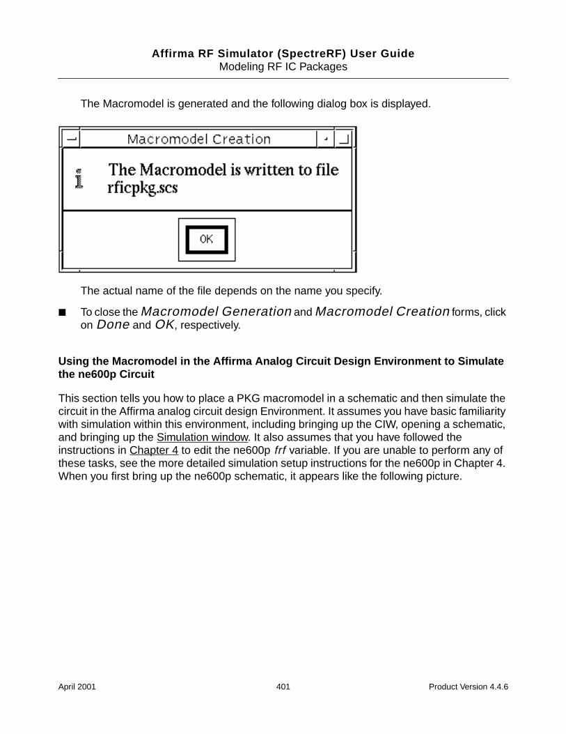
Affirma RF Simulator (SpectreRF) User GuideModeling RF IC Packages
The Macromodel is generated and the following dialog box is displayed.
The actual name of the file depends on the name you specify.
To close the Macromodel Generation and Macromodel Creation forms, clickon Done and OK, respectively.
Using the Macromodel in the Affirma Analog Circuit Design Environment to Simulatethe ne600p Circuit
This section tells you how to place a PKG macromodel in a schematic and then simulate thecircuit in the Affirma analog circuit design Environment. It assumes you have basic familiaritywith simulation within this environment, including bringing up the CIW, opening a schematic,and bringing up the Simulation window. It also assumes that you have followed theinstructions in Chapter 4 to edit the ne600p frf variable. If you are unable to perform any ofthese tasks, see the more detailed simulation setup instructions for the ne600p in Chapter 4.When you first bring up the ne600p schematic, it appears like the following picture.
April 2001 401 Product Version 4.4.6
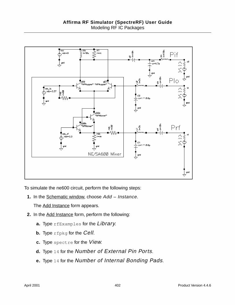
Affirma RF Simulator (SpectreRF) User GuideModeling RF IC Packages
To simulate the ne600 circuit, perform the following steps:
1. In the Schematic window, choose Add – Instance.
The Add Instance form appears.
2. In the Add Instance form, perform the following:
a. Type rfExamples for the Library.
b. Type rfpkg for the Cell.
c. Type spectre for the View.
d. Type 14 for the Number of External Pin Ports.
e. Type 14 for the Number of Internal Bonding Pads.
April 2001 402 Product Version 4.4.6
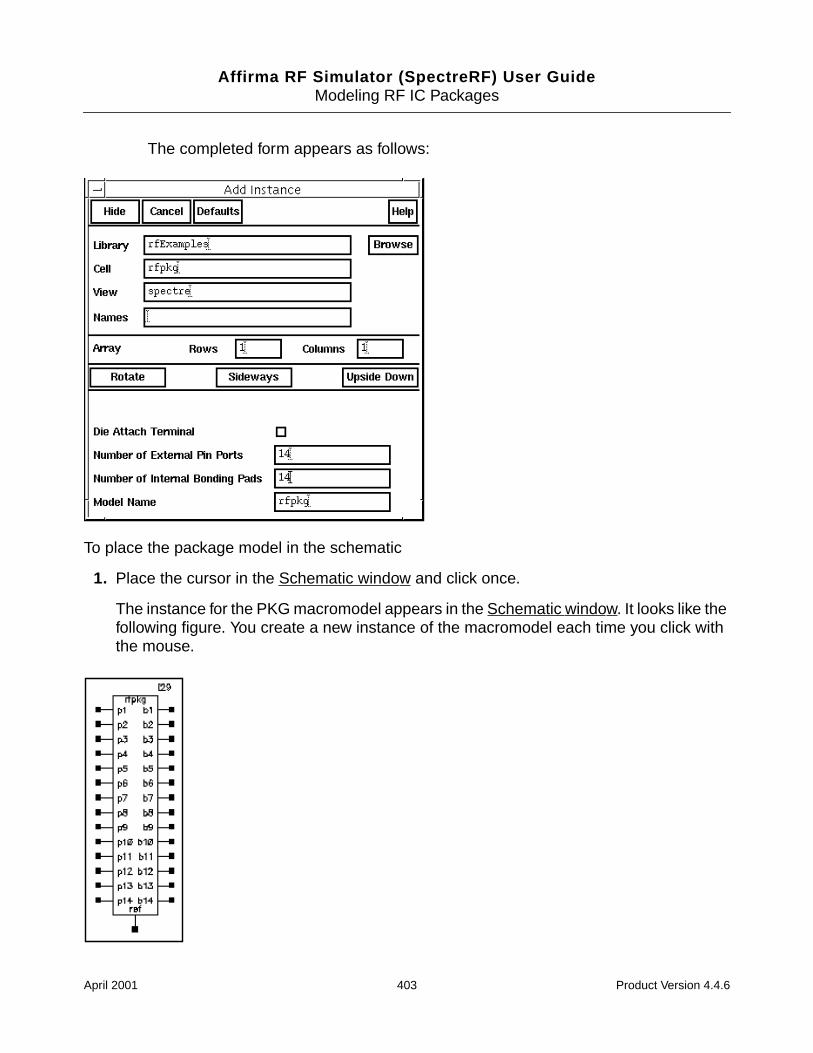
Affirma RF Simulator (SpectreRF) User GuideModeling RF IC Packages
The completed form appears as follows:
To place the package model in the schematic
1. Place the cursor in the Schematic window and click once.
The instance for the PKG macromodel appears in the Schematic window. It looks like thefollowing figure. You create a new instance of the macromodel each time you click withthe mouse.
April 2001 403 Product Version 4.4.6
Affirma RF Simulator (SpectreRF) User GuideModeling RF IC Packages
2. With your cursor in the Schematic window, press the Escape key.
The Add Instance form closes, and clicking with the mouse no longer creates newinstances.
3. In the Schematic window, choose Edit – Properties – Objects.
The Edit Object Properties form appears.
4. In the Schematic window, select the PKG macromodel that you placed in the window.
The Edit Object Properties form changes to accept specifications for the macromodel.
April 2001 404 Product Version 4.4.6
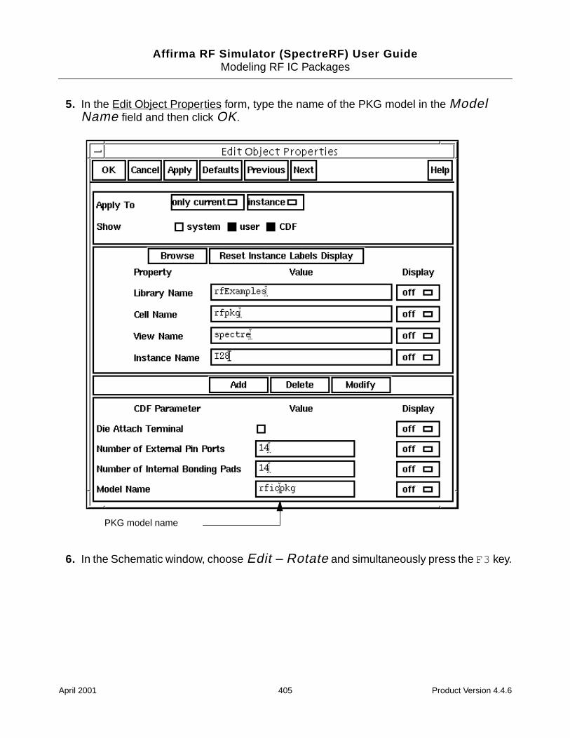
Affirma RF Simulator (SpectreRF) User GuideModeling RF IC Packages
5. In the Edit Object Properties form, type the name of the PKG model in the ModelName field and then click OK.
6. In the Schematic window, choose Edit – Rotate and simultaneously press the F3 key.
PKG model name
April 2001 405 Product Version 4.4.6
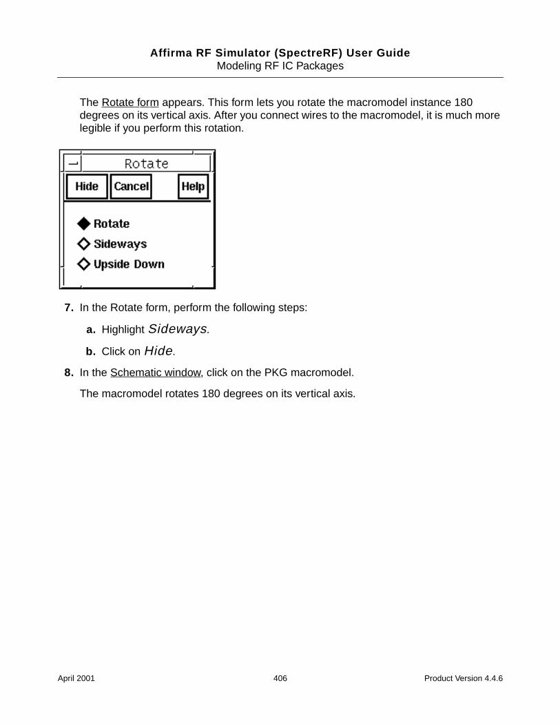
Affirma RF Simulator (SpectreRF) User GuideModeling RF IC Packages
The Rotate form appears. This form lets you rotate the macromodel instance 180degrees on its vertical axis. After you connect wires to the macromodel, it is much morelegible if you perform this rotation.
7. In the Rotate form, perform the following steps:
a. Highlight Sideways.
b. Click on Hide.
8. In the Schematic window, click on the PKG macromodel.
The macromodel rotates 180 degrees on its vertical axis.
April 2001 406 Product Version 4.4.6
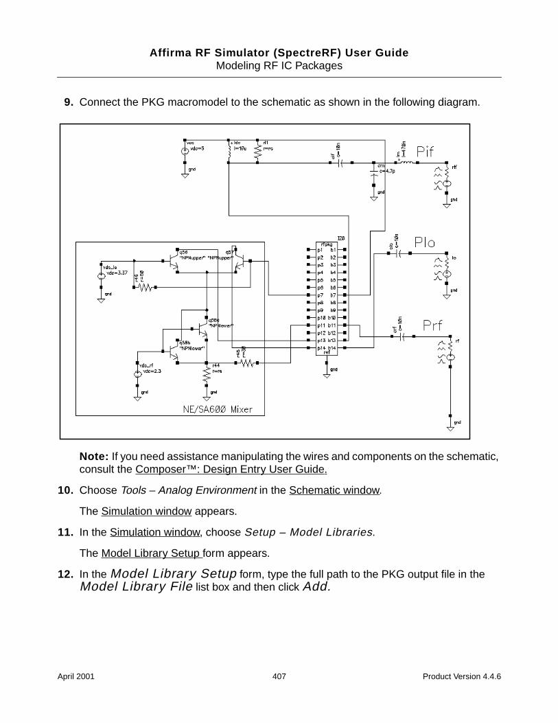
Affirma RF Simulator (SpectreRF) User GuideModeling RF IC Packages
9. Connect the PKG macromodel to the schematic as shown in the following diagram.
Note: If you need assistance manipulating the wires and components on the schematic,consult the Composer™: Design Entry User Guide.
10. Choose Tools – Analog Environment in the Schematic window.
The Simulation window appears.
11. In the Simulation window, choose Setup – Model Libraries.
The Model Library Setup form appears.
12. In the Model Library Setup form, type the full path to the PKG output file in theModel Library File list box and then click Add.
April 2001 407 Product Version 4.4.6
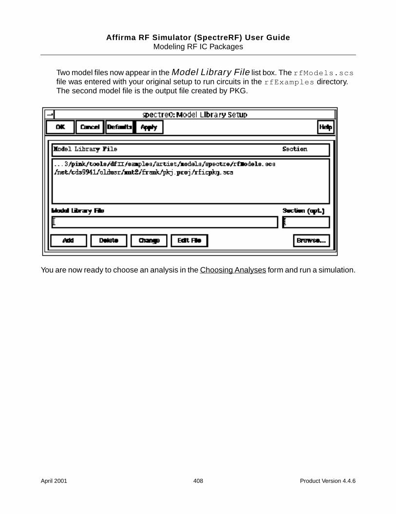
Affirma RF Simulator (SpectreRF) User GuideModeling RF IC Packages
Two model files now appear in the Model Library File list box. The rfModels.scsfile was entered with your original setup to run circuits in the rfExamples directory.The second model file is the output file created by PKG.
You are now ready to choose an analysis in the Choosing Analyses form and run a simulation.
April 2001 408 Product Version 4.4.6
Affirma RF Simulator (SpectreRF) User Guide
9Extracting K-Models
The K-model links SpectreRF and Alta™ SPW as shown in the Figure below. The Oceanextraction script automatically runs a set of SpectreRF analyses and writes the results to adirectory you specify. The results characterize the baseband performance of the RF circuit.There are three kinds of K-models.
Transmitter: This is actually a J-model and is discussed in chapter 10.
Receiver (linear): This is a linearized model of the receiver. It includes noise except forphase noise. Extraction is very similar to extraction of the non-linear K-model.
Receiver (non-linear): This is a noiseless non-linear model of the receiver.
The receiver K-models only exist in the Cierto™ Alta SPW RF library but you extract the K-model data using SpectreRF in the Affirma analog circuit design Environment.
This chapter describes the following:
The procedure for extracting a non-linear receiver K-model.
The K-model’s limitations
The procedure for handling strong out-of-band blockers
The K-model data files and their format are described at the end of the chapter.
April 2001 409 Product Version 4.4.6
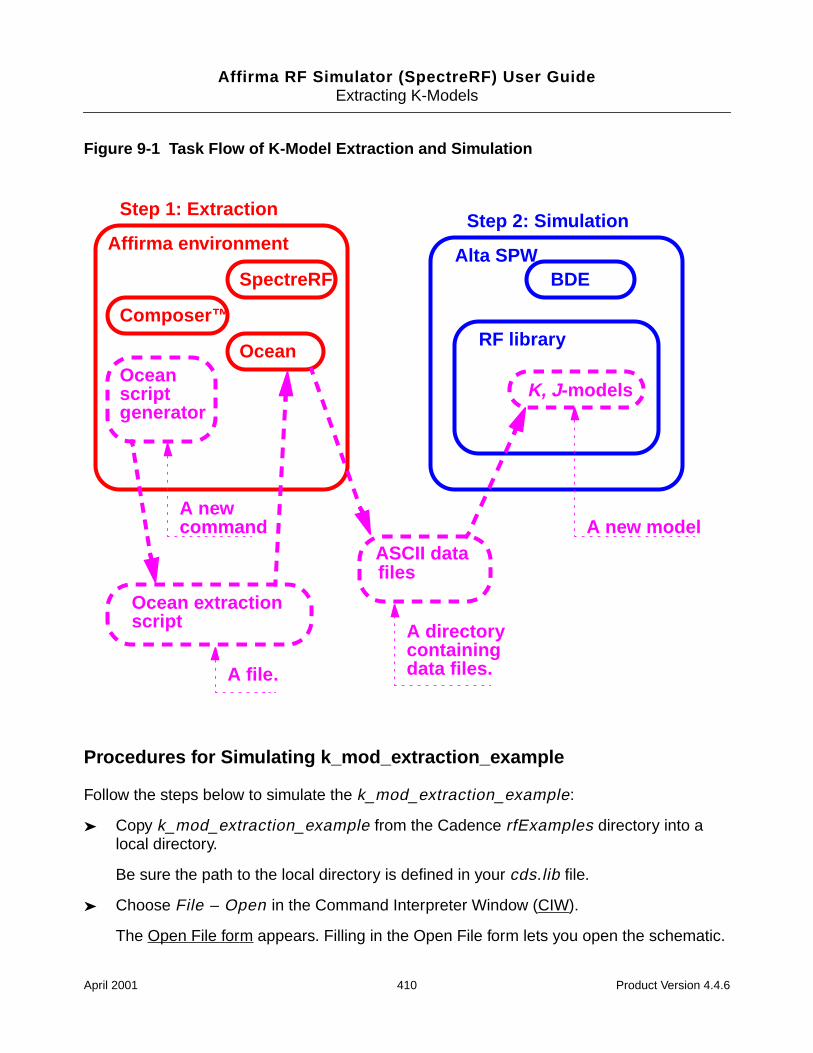
Affirma RF Simulator (SpectreRF) User GuideExtracting K-Models
Figure 9-1 Task Flow of K-Model Extraction and Simulation
Procedures for Simulating k_mod_extraction_example
Follow the steps below to simulate the k_mod_extraction_example:
Copy k_mod_extraction_example from the Cadence rfExamples directory into alocal directory.
Be sure the path to the local directory is defined in your cds.lib file.
Choose File – Open in the Command Interpreter Window (CIW).
The Open File form appears. Filling in the Open File form lets you open the schematic.
Affirma environment
Composer™
SpectreRF
OceanOceanscriptgenerator
Alta SPWBDE
RF library
K, J-models
ASCII datafiles
Ocean extractionscript
A newcommand
A file.
A directorycontainingdata files.
A new model
Step 1: ExtractionStep 2: Simulation
April 2001 410 Product Version 4.4.6
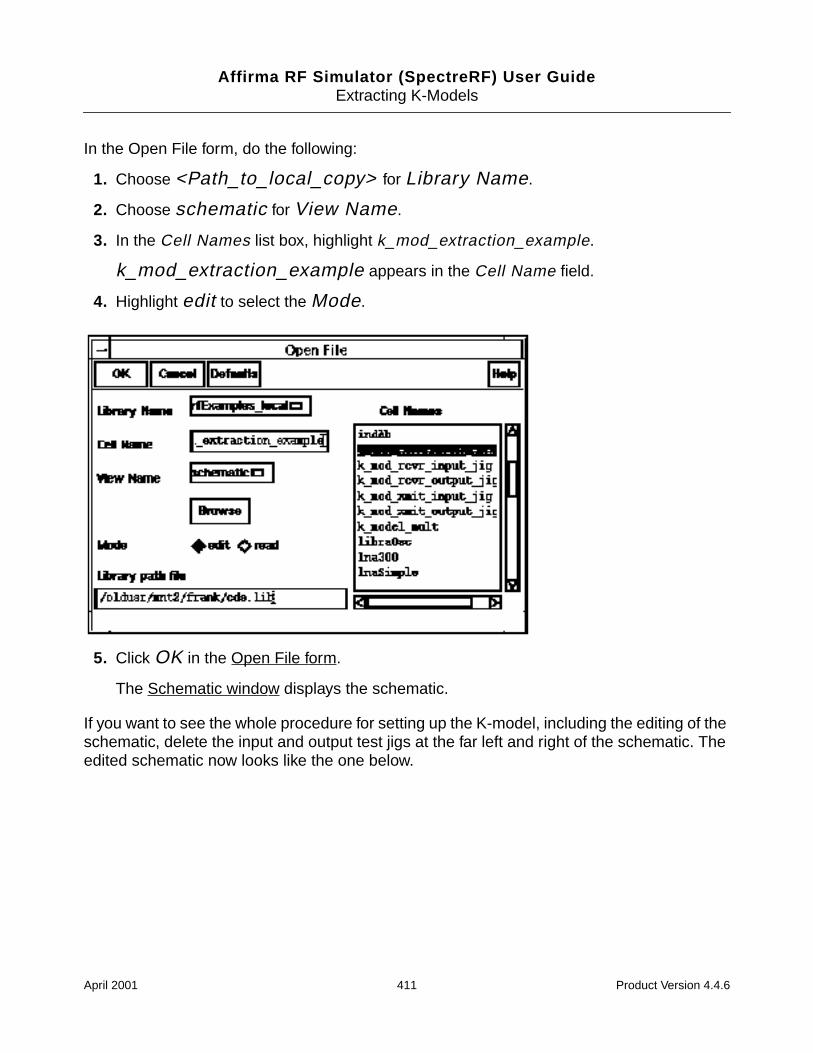
Affirma RF Simulator (SpectreRF) User GuideExtracting K-Models
In the Open File form, do the following:
1. Choose <Path_to_local_copy> for Library Name.
2. Choose schematic for View Name.
3. In the Cell Names list box, highlight k_mod_extraction_example.
k_mod_extraction_example appears in the Cell Name field.
4. Highlight edit to select the Mode.
5. Click OK in the Open File form.
The Schematic window displays the schematic.
If you want to see the whole procedure for setting up the K-model, including the editing of theschematic, delete the input and output test jigs at the far left and right of the schematic. Theedited schematic now looks like the one below.
April 2001 411 Product Version 4.4.6
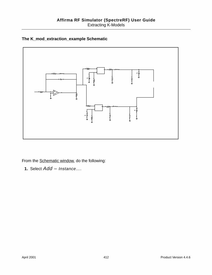
Affirma RF Simulator (SpectreRF) User GuideExtracting K-Models
The K_mod_extraction_example Schematic
From the Schematic window, do the following:
1. Select Add – Instance….
April 2001 412 Product Version 4.4.6
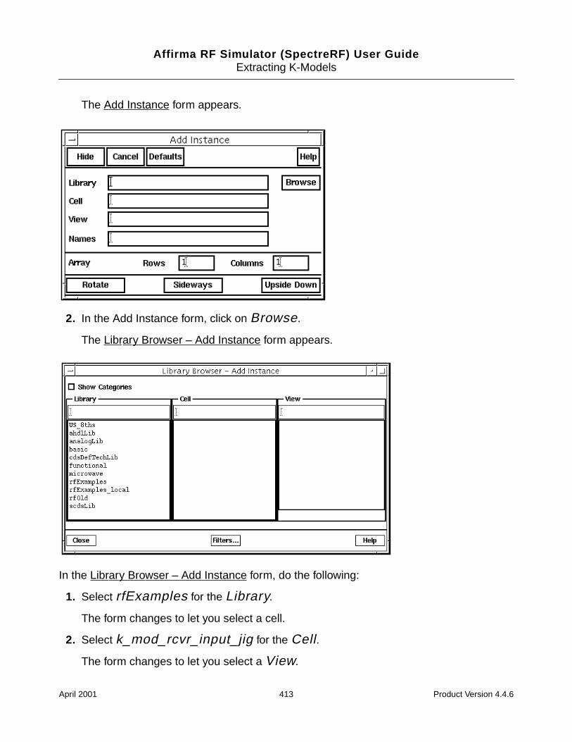
Affirma RF Simulator (SpectreRF) User GuideExtracting K-Models
The Add Instance form appears.
2. In the Add Instance form, click on Browse.
The Library Browser – Add Instance form appears.
In the Library Browser – Add Instance form, do the following:
1. Select rfExamples for the Library.
The form changes to let you select a cell.
2. Select k_mod_rcvr_input_jig for the Cell.
The form changes to let you select a View.
April 2001 413 Product Version 4.4.6
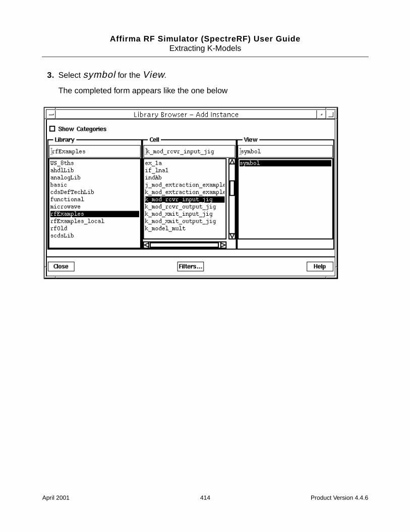
Affirma RF Simulator (SpectreRF) User GuideExtracting K-Models
3. Select symbol for the View.
The completed form appears like the one below
April 2001 414 Product Version 4.4.6
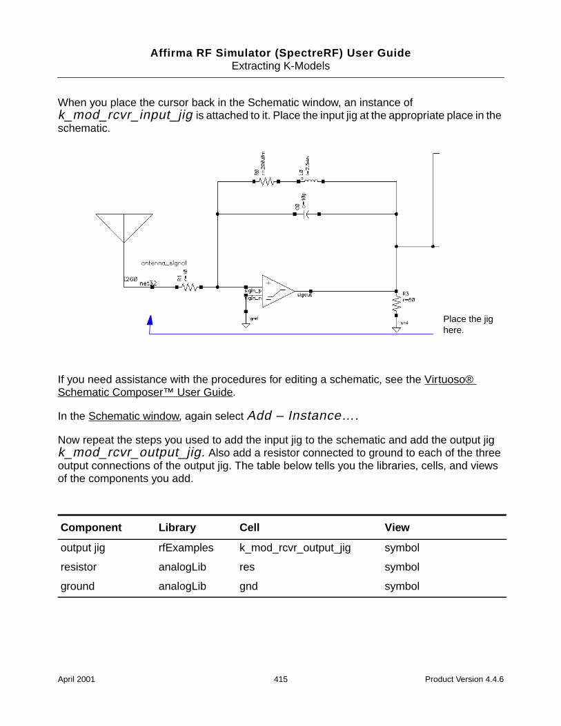
Affirma RF Simulator (SpectreRF) User GuideExtracting K-Models
When you place the cursor back in the Schematic window, an instance ofk_mod_rcvr_input_jig is attached to it. Place the input jig at the appropriate place in theschematic.
If you need assistance with the procedures for editing a schematic, see the Virtuoso®Schematic Composer™ User Guide.
In the Schematic window, again select Add – Instance….
Now repeat the steps you used to add the input jig to the schematic and add the output jigk_mod_rcvr_output_jig. Also add a resistor connected to ground to each of the threeoutput connections of the output jig. The table below tells you the libraries, cells, and viewsof the components you add.
Component Library Cell View
output jig rfExamples k_mod_rcvr_output_jig symbol
resistor analogLib res symbol
ground analogLib gnd symbol
Place the jighere.
April 2001 415 Product Version 4.4.6
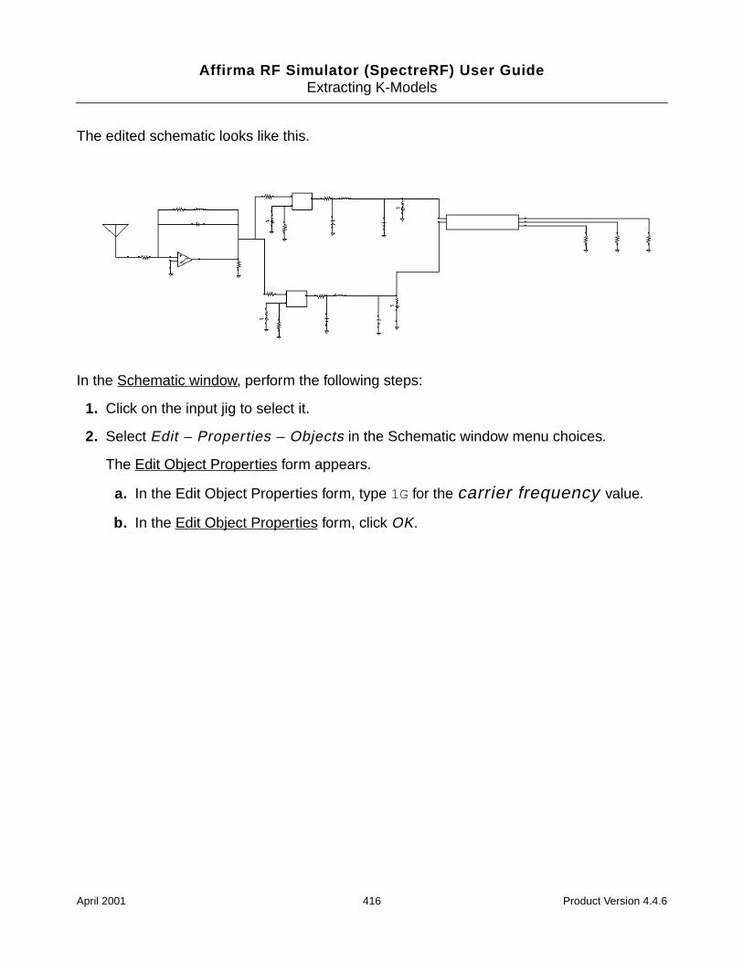
Affirma RF Simulator (SpectreRF) User GuideExtracting K-Models
The edited schematic looks like this.
In the Schematic window, perform the following steps:
1. Click on the input jig to select it.
2. Select Edit – Properties – Objects in the Schematic window menu choices.
The Edit Object Properties form appears.
a. In the Edit Object Properties form, type 1G for the carrier frequency value.
b. In the Edit Object Properties form, click OK.
April 2001 416 Product Version 4.4.6
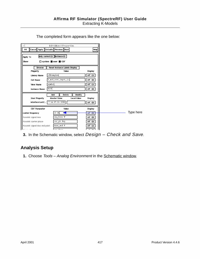
Affirma RF Simulator (SpectreRF) User GuideExtracting K-Models
The completed form appears like the one below:
3. In the Schematic window, select Design – Check and Save.
Analysis Setup
1. Choose Tools – Analog Environment in the Schematic window.
Type here
April 2001 417 Product Version 4.4.6
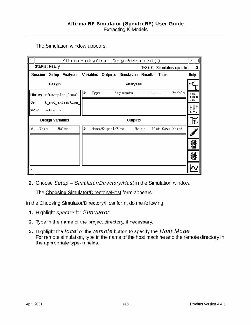
Affirma RF Simulator (SpectreRF) User GuideExtracting K-Models
The Simulation window appears.
2. Choose Setup – Simulator/Directory/Host in the Simulation window.
The Choosing Simulator/Directory/Host form appears.
In the Choosing Simulator/Directory/Host form, do the following:
1. Highlight spectre for Simulator.
2. Type in the name of the project directory, if necessary.
3. Highlight the local or the remote button to specify the Host Mode.For remote simulation, type in the name of the host machine and the remote directory inthe appropriate type-in fields.
April 2001 418 Product Version 4.4.6
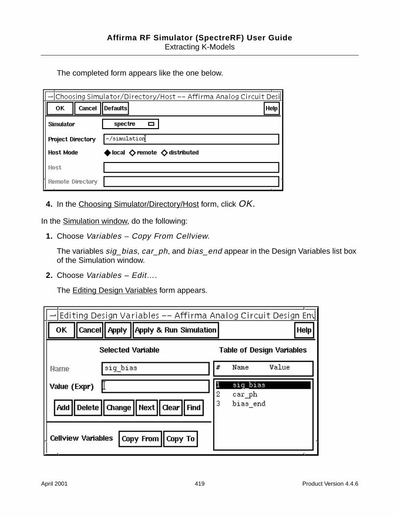
Affirma RF Simulator (SpectreRF) User GuideExtracting K-Models
The completed form appears like the one below.
4. In the Choosing Simulator/Directory/Host form, click OK.
In the Simulation window, do the following:
1. Choose Variables – Copy From Cellview.
The variables sig_bias, car_ph, and bias_end appear in the Design Variables list boxof the Simulation window.
2. Choose Variables – Edit….
The Editing Design Variables form appears.
April 2001 419 Product Version 4.4.6
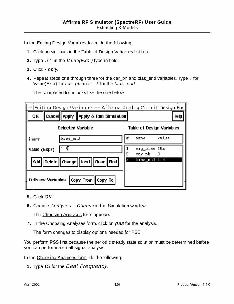
Affirma RF Simulator (SpectreRF) User GuideExtracting K-Models
In the Editing Design Variables form, do the following:
1. Click on sig_bias in the Table of Design Variables list box.
2. Type .01 in the Value(Expr) type-in field.
3. Click Apply.
4. Repeat steps one through three for the car_ph and bias_end variables. Type 0 forValue(Expr) for car_ph and 1.8 for the bias_end.
The completed form looks like the one below:
5. Click OK.
6. Choose Analyses – Choose in the Simulation window.
The Choosing Analyses form appears.
7. In the Choosing Analyses form, click on pss for the analysis.
The form changes to display options needed for PSS.
You perform PSS first because the periodic steady state solution must be determined beforeyou can perform a small-signal analysis.
In the Choosing Analyses form, do the following:
1. Type 1G for the Beat Frequency.
April 2001 420 Product Version 4.4.6
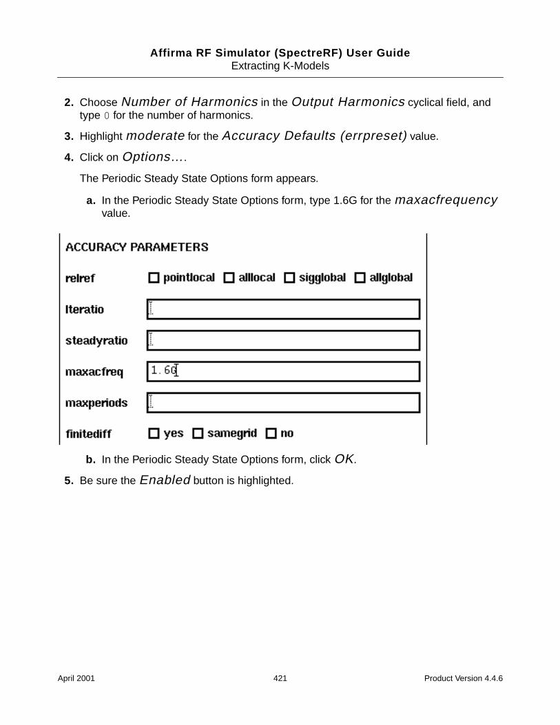
Affirma RF Simulator (SpectreRF) User GuideExtracting K-Models
2. Choose Number of Harmonics in the Output Harmonics cyclical field, andtype 0 for the number of harmonics.
3. Highlight moderate for the Accuracy Defaults (errpreset) value.
4. Click on Options….
The Periodic Steady State Options form appears.
a. In the Periodic Steady State Options form, type 1.6G for the maxacfrequencyvalue.
b. In the Periodic Steady State Options form, click OK.
5. Be sure the Enabled button is highlighted.
April 2001 421 Product Version 4.4.6
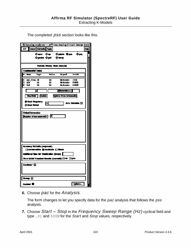
Affirma RF Simulator (SpectreRF) User GuideExtracting K-Models
The completed pss section looks like this.
6. Choose pac for the Analysis.
The form changes to let you specify data for the pac analysis that follows the pssanalysis.
7. Choose Start – Stop in the Frequency Sweep Range (Hz) cyclical field andtype .01 and 500M for the Start and Stop values, respectively.
April 2001 422 Product Version 4.4.6
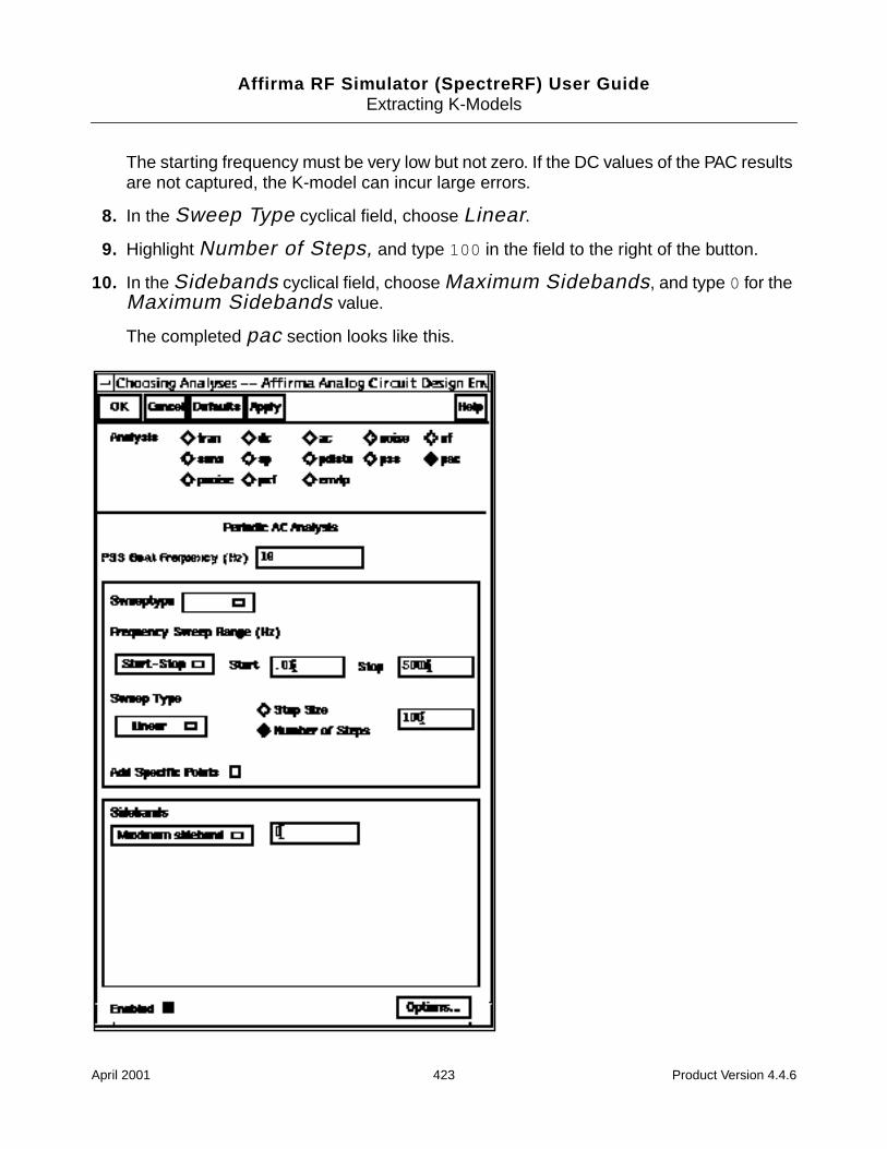
Affirma RF Simulator (SpectreRF) User GuideExtracting K-Models
The starting frequency must be very low but not zero. If the DC values of the PAC resultsare not captured, the K-model can incur large errors.
8. In the Sweep Type cyclical field, choose Linear.
9. Highlight Number of Steps, and type 100 in the field to the right of the button.
10. In the Sidebands cyclical field, choose Maximum Sidebands, and type 0 for theMaximum Sidebands value.
The completed pac section looks like this.
April 2001 423 Product Version 4.4.6
Affirma RF Simulator (SpectreRF) User GuideExtracting K-Models
11. Click OK in the Choosing Analyses form.
Running the Simulation
1. In the Simulation window, select Simulation – Netlist and Run to run the simulation.
The output log file appears and displays information about the simulation as it runs.Check the CIW for a message saying the simulation completed successfully.
Checking the Simulation Results
Choose Results – Direct Plot – PSS in the Simulation Window.
The Waveform window and the PSS Results form appear.
In the PSS Results form, do the following:
1. Choose Replace for Plot Mode.
2. Choose pac for Analysis Type.
3. Choose Voltage for Function.
4. Choose Magnitude for Modifier.
April 2001 424 Product Version 4.4.6
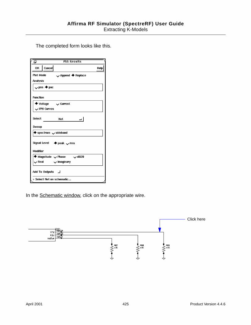
Affirma RF Simulator (SpectreRF) User GuideExtracting K-Models
The completed form looks like this.
In the Schematic window, click on the appropriate wire.
Click here
April 2001 425 Product Version 4.4.6
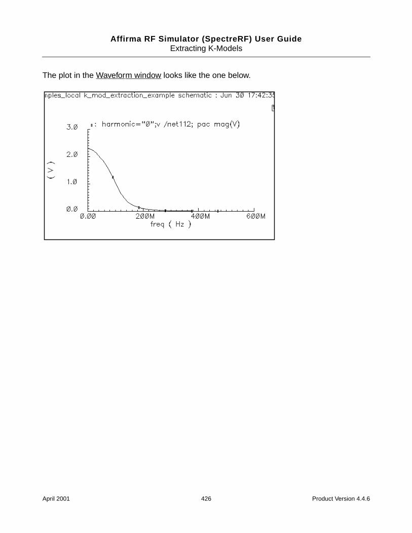
Affirma RF Simulator (SpectreRF) User GuideExtracting K-Models
The plot in the Waveform window looks like the one below.
April 2001 426 Product Version 4.4.6
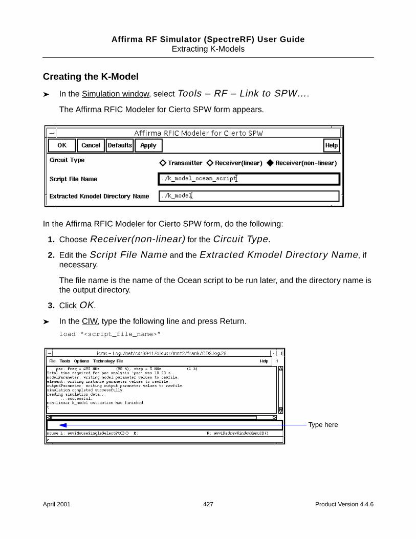
Affirma RF Simulator (SpectreRF) User GuideExtracting K-Models
Creating the K-Model
In the Simulation window, select Tools – RF – Link to SPW….
The Affirma RFIC Modeler for Cierto SPW form appears.
In the Affirma RFIC Modeler for Cierto SPW form, do the following:
1. Choose Receiver(non-linear) for the Circuit Type.
2. Edit the Script File Name and the Extracted Kmodel Directory Name, ifnecessary.
The file name is the name of the Ocean script to be run later, and the directory name isthe output directory.
3. Click OK.
In the CIW, type the following line and press Return.
load “<script_file_name>”
Type here
April 2001 427 Product Version 4.4.6
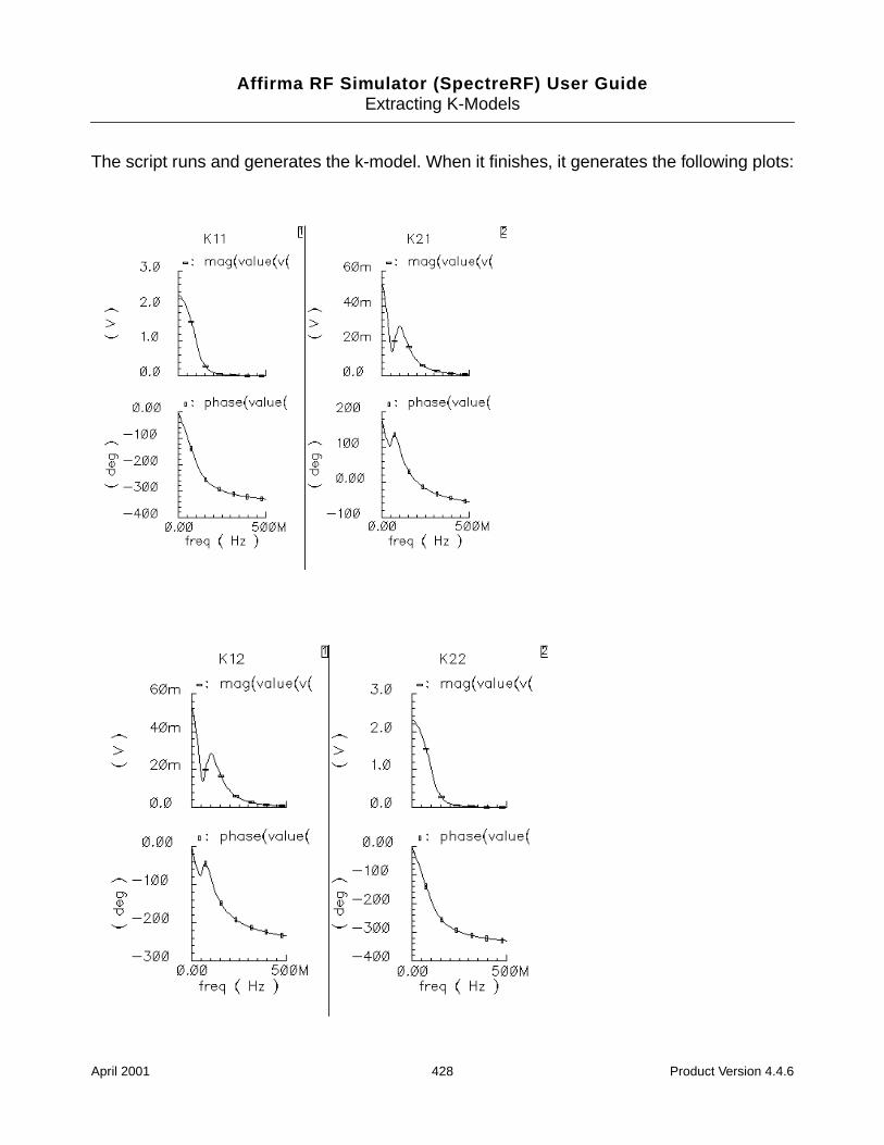
Affirma RF Simulator (SpectreRF) User GuideExtracting K-Models
The script runs and generates the k-model. When it finishes, it generates the following plots:
April 2001 428 Product Version 4.4.6
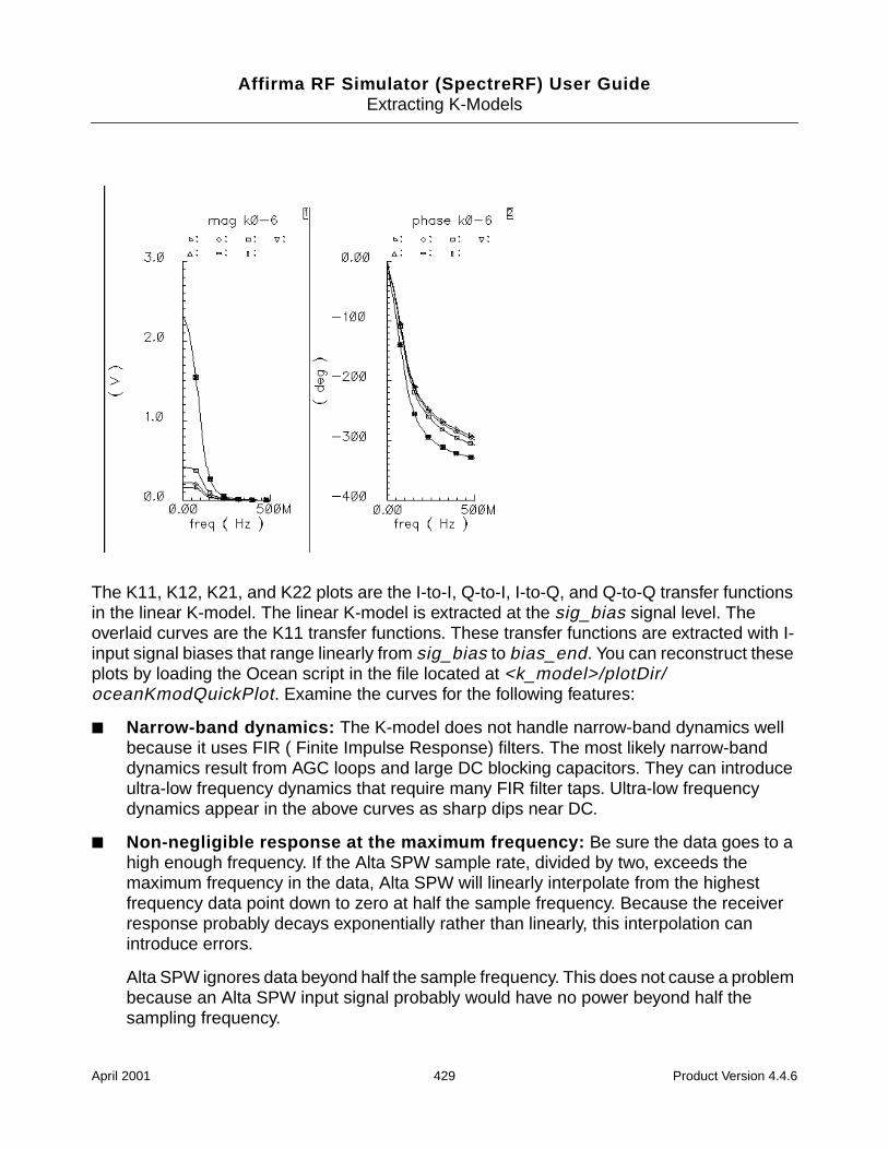
Affirma RF Simulator (SpectreRF) User GuideExtracting K-Models
The K11, K12, K21, and K22 plots are the I-to-I, Q-to-I, I-to-Q, and Q-to-Q transfer functionsin the linear K-model. The linear K-model is extracted at the sig_bias signal level. Theoverlaid curves are the K11 transfer functions. These transfer functions are extracted with I-input signal biases that range linearly from sig_bias to bias_end. You can reconstruct theseplots by loading the Ocean script in the file located at <k_model>/plotDir/oceanKmodQuickPlot. Examine the curves for the following features:
Narrow-band dynamics: The K-model does not handle narrow-band dynamics wellbecause it uses FIR ( Finite Impulse Response) filters. The most likely narrow-banddynamics result from AGC loops and large DC blocking capacitors. They can introduceultra-low frequency dynamics that require many FIR filter taps. Ultra-low frequencydynamics appear in the above curves as sharp dips near DC.
Non-negligible response at the maximum frequency: Be sure the data goes to ahigh enough frequency. If the Alta SPW sample rate, divided by two, exceeds themaximum frequency in the data, Alta SPW will linearly interpolate from the highestfrequency data point down to zero at half the sample frequency. Because the receiverresponse probably decays exponentially rather than linearly, this interpolation canintroduce errors.
Alta SPW ignores data beyond half the sample frequency. This does not cause a problembecause an Alta SPW input signal probably would have no power beyond half thesampling frequency.
April 2001 429 Product Version 4.4.6

Affirma RF Simulator (SpectreRF) User GuideExtracting K-Models
More About the K-Model
Like any behavioral model, the K-model has limitations and requirements. The assumptionson which the K-model is based cause the basic limitations. Other limitations are caused bypractical considerations. There are also requirements that are specific to the Alta SPWenvironment. Finally, this section discusses some limitations of the K-model’s ability to modelout-of-band blockers.
Limitations and requirements resulting from linear K-model assumptions
The linear K-model makes the following two assumptions beyond the small signalassumption:
Unless the SpectreRF model includes detailed A/D converter models, the extractedlinear K-model assumes that noise at the base-band outputs does not changesignificantly over the A/D aperture time.
The first K-model assumption involves noise and A/D conversion. The linear modelincludes noise generated within the front end 1. "Aperture time" is the time the A./Dconverter requires just to measure a voltage, not to measure and hold it. The assumptionis that the noise is constant over the aperture time. This implies the noise is band limited.However, as the following discussion explains, the noise bandwidth must also not be toosmall.
The two equivalent output noise sources, one for the I output and one for the Q output,are uncorrelated.
Frequently, much of the noisy circuitry is common to both outputs. Despite the commoncircuitry, the K-model assumes the two output noise signals are independent. This is agood assumption if the noise is white over the frequencies of interest. In summary, thenoise must be white with respect to filters preceding the A/D conversion but band-limitedwith respect to 1/(aperture time).
Why isn’t there just one K-model, a noisy non-linear K-model instead of a noisy linear K-model and a noise-less non-linear K-model? Putting small signal noise in the non-linearK-model would suggest that the model’s noise varied with input power. It does not.Furthermore, noise analysis is usually of interest in bit error rate simulations. Suchsimulations are usually long and the desired signal is weak. The linear K-model sufficesfor weak desired signals and runs faster than the non-linear K-model.
1. The linear model does not account for phase noise. However, if one knows the power spectral density ofthe phase noise one can easily follow the K-model with a complex multiplier that shifts the phase of the K-model output. A filter driven by white Gaussian noise would generate the random phase shift.
April 2001 430 Product Version 4.4.6
Affirma RF Simulator (SpectreRF) User GuideExtracting K-Models
Limitations and requirements resulting from non-linear K-model assumptions
The K-model requires two basic assumptions:
Small-signal components of the base-band input can be wide-band, but largecomponents must fall within the receiver’s bandwidth.
The signal of interest is usually within the receiver’s bandwidth, and interferers usually lieoutside this bandwidth. However, if the receiver has a band selection filter immediatelyafter the antenna, and that filter can be modeled apart from the K-model, this firstassumption is not a severe restriction. This is true because the filter makes the interferersmall by the time it reaches the K-model.
Non-linear behavior depends only on the input radius1. Non-linear PM/PM and PM/AMeffects are negligible.
Requirements resulting from the Alta SPW environment
Both K-models are part of Alta SPW, the Cierto Signal Processing Worksystem. AltaSPW is a DSP design tool. This environment creates the following two consequencesyou must remember:
Model extraction requires base-band input and output ports.
Because it is a base-band tool, Alta SPW operates on the information impressed on theRF carrier rather than the instantaneous value of the RF signal. Each of two carrierphases, sine and cosine, carry information. Because Alta SPW represents base-bandsignals as complex numbers, the modeled RF circuit must have base-band input andoutput ports.
The input test jig creates the input port. The input test jig mixes the base-band inputsignal up to the appropriate carrier frequency, thereby synthesizing an antenna signalfrom a base-band input. Changing the phase of the carrier by 90 degrees switches thebase-band input between the "in-phase" and "quadrature" input ports. The Oceanextraction script changes carrier phase automatically when it extracts a K-model.
If the circuitry does not contain two base-band output ports, you must synthesize them.You can synthesize them easily using ideal behavioral elements. For example, to build aK-model of only the low noise amplifier, you add ideal downconverters to the SpectreRFmodel and extract a K-model of the combination.
1. If the input signal is rf(t) = a(t) cos(wct)-b(t) sin(wct), the base-band signal is a(t)+j b(t), a trajectory in thecomplex plane. This is the rectangular representation. The polar representation is in terms of radius andangle. The radius is Sqrt[a(t) a(t)+b(t) b(t)]. The angle is ArcTan[b(t)/a(t)].
April 2001 431 Product Version 4.4.6
Affirma RF Simulator (SpectreRF) User GuideExtracting K-Models
You can partition a receiver into smaller K-models only if there is no non-linear interstageloading at the break points and if the carrier fundamental is the only important quantity.
The input and output test jigs also tell the extraction script where to excite the SpectreRFmodel and what quantities to measure.
The SpectreRF noise analysis must extend far enough to capture all important features,including those beyond half the Alta SPW sampling frequency.
This is true because the power spectral density suffers aliasing in the DSP environment.The only data available for DSP is for discrete, evenly-spaced time-points. This restrictionimposes a constraint on possible input signals that is usually met within the design.Specified input signals must not have significant power beyond half the samplingfrequency. 1 Because the noise is not a signal you specify, it need not meet thatconstraint. Noise power that is well beyond half the sampling frequency can alias downto the band of interest. If the noise is characterized to a high-enough frequency, the K-model automatically aliases it.
Practical limitations of the K-model
Image rejection
Although the K-model theoretically models image rejection, such modeling is notpractical for the Alta SPW implementation Figure 9-2 on page 433 shows how the carrier,local oscillator, and image frequencies can be related. The Alta SPW sampling frequencyis probably approximately the bandwidth of the RF receiver, shown in blue. To simulatedynamics at the image frequency, the Alta SPW sampling frequency must span twice thedifference between the carrier frequency and the image frequency. Such a high samplingfrequency requires an impractical number of FIR filter taps to model the receiverdynamics. Simulation time is almost as lengthy as with an unsuppressed carriersimulation.
1. The channel and RF front end are cascaded physical entities with no sampler between them. But becausethey are modeled in Alta SPW as separate blocks, Alta SPW implicitly assumes an ideal sampler lies be-tween the channel and front end. That assumption is only valid for base-band signals that have no signif-icant spectral components near or beyond half the sampling frequency. If that assumption were not validthe overall design would have far more serious problems than K-model accuracy.
April 2001 432 Product Version 4.4.6
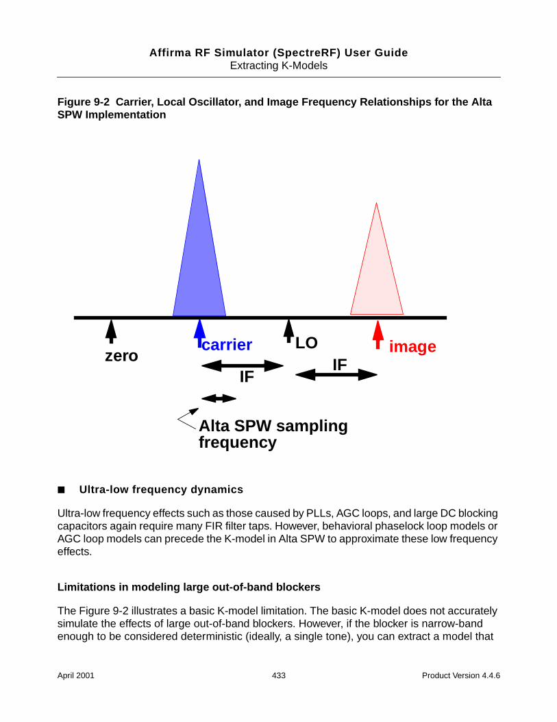
Affirma RF Simulator (SpectreRF) User GuideExtracting K-Models
Figure 9-2 Carrier, Local Oscillator, and Image Frequency Relationships for the AltaSPW Implementation
Ultra-low frequency dynamics
Ultra-low frequency effects such as those caused by PLLs, AGC loops, and large DC blockingcapacitors again require many FIR filter taps. However, behavioral phaselock loop models orAGC loop models can precede the K-model in Alta SPW to approximate these low frequencyeffects.
Limitations in modeling large out-of-band blockers
The Figure 9-2 illustrates a basic K-model limitation. The basic K-model does not accuratelysimulate the effects of large out-of-band blockers. However, if the blocker is narrow-bandenough to be considered deterministic (ideally, a single tone), you can extract a model that
carrier LO
IF
imagezero IF
Alta SPW samplingfrequency
April 2001 433 Product Version 4.4.6
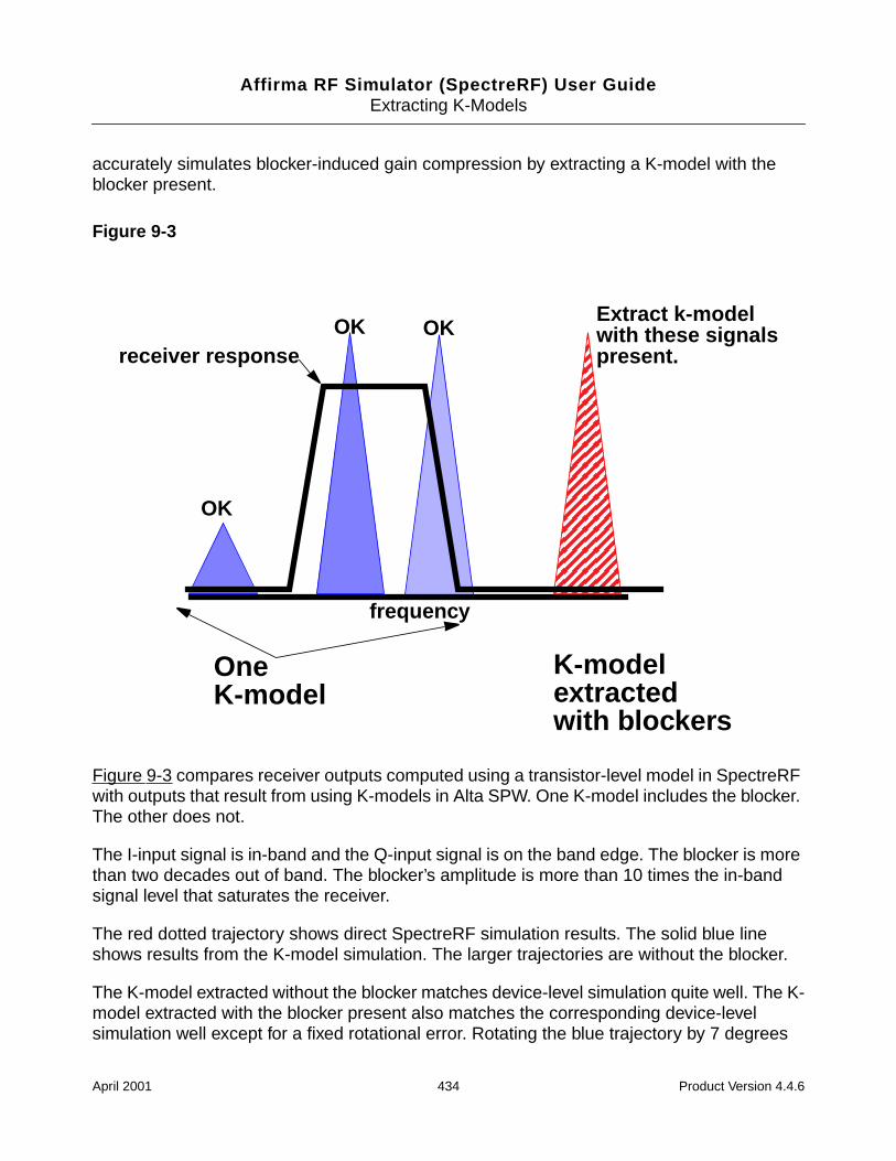
Affirma RF Simulator (SpectreRF) User GuideExtracting K-Models
accurately simulates blocker-induced gain compression by extracting a K-model with theblocker present.
Figure 9-3
Figure 9-3 compares receiver outputs computed using a transistor-level model in SpectreRFwith outputs that result from using K-models in Alta SPW. One K-model includes the blocker.The other does not.
The I-input signal is in-band and the Q-input signal is on the band edge. The blocker is morethan two decades out of band. The blocker’s amplitude is more than 10 times the in-bandsignal level that saturates the receiver.
The red dotted trajectory shows direct SpectreRF simulation results. The solid blue lineshows results from the K-model simulation. The larger trajectories are without the blocker.
The K-model extracted without the blocker matches device-level simulation quite well. The K-model extracted with the blocker present also matches the corresponding device-levelsimulation well except for a fixed rotational error. Rotating the blue trajectory by 7 degrees
OK
frequency
OK
OKreceiver response
Extract k-modelwith these signalspresent.
One K-modelK-model extracted
with blockers
April 2001 434 Product Version 4.4.6
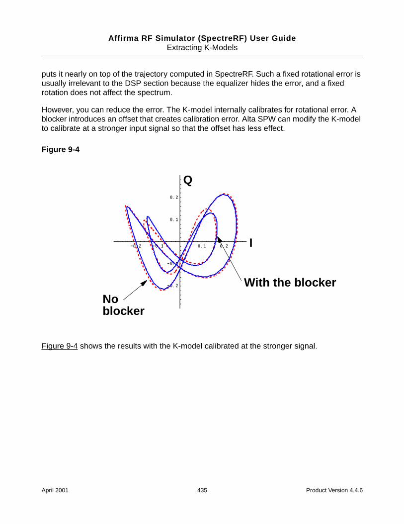
Affirma RF Simulator (SpectreRF) User GuideExtracting K-Models
puts it nearly on top of the trajectory computed in SpectreRF. Such a fixed rotational error isusually irrelevant to the DSP section because the equalizer hides the error, and a fixedrotation does not affect the spectrum.
However, you can reduce the error. The K-model internally calibrates for rotational error. Ablocker introduces an offset that creates calibration error. Alta SPW can modify the K-modelto calibrate at a stronger input signal so that the offset has less effect.
Figure 9-4
Figure 9-4 shows the results with the K-model calibrated at the stronger signal.
I
Q
Noblocker
With the blocker
April 2001 435 Product Version 4.4.6
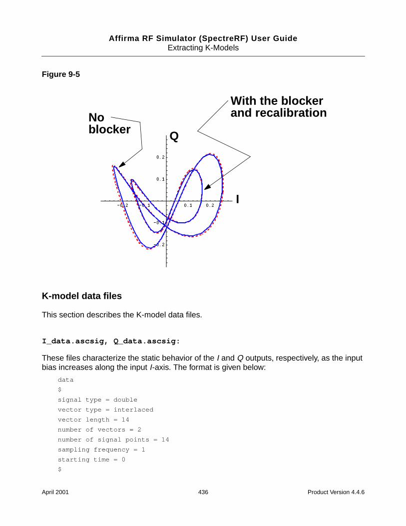
Affirma RF Simulator (SpectreRF) User GuideExtracting K-Models
Figure 9-5
K-model data files
This section describes the K-model data files.
I_data.ascsig, Q_data.ascsig:
These files characterize the static behavior of the I and Q outputs, respectively, as the inputbias increases along the input I-axis. The format is given below:
data
$
signal type = double
vector type = interlaced
vector length = 14
number of vectors = 2
number of signal points = 14
sampling frequency = 1
starting time = 0
$
I
Q
Noblocker
With the blockerand recalibration
April 2001 436 Product Version 4.4.6
Affirma RF Simulator (SpectreRF) User GuideExtracting K-Models
0.001 0.002300
0.3008333 0.692013
0.6006667 1.381728
0.9005 2.071483
1.200333 2.568851
1.500167 2.655311
1.8 2.710871
dck
This file contains the lowest frequency gains of the K11 and K21 transfer functions. Theformat is shown below:
2.299950
-0.051965
sig_biases
This file lists the input signal biases. The format is shown below:
0.001
0.3008333
0.6006667
0.9005
1.200333
1.500167
1.8
psd_I.ascsig, psd_Q.ascsig
These files contain the power spectral densities of the noise observed at the baseband I andQ outputs. The first column is frequency, and the second column is power spectral density involts/Sqrt(Hz). The format is given below:
# wavew4s1i1() from 10e-3 to 25e6
# wavew4s1i1()
10e-3 1.334e-6
250e3 943.1e-9
500e3 943.1e-9
750e3 943e-9
1e6 942.7e-9
1.25e6 942.4e-9
April 2001 437 Product Version 4.4.6
Affirma RF Simulator (SpectreRF) User GuideExtracting K-Models
1.5e6 941.8e-9
1.75e6 940.9e-9
2e6 939.6e-9
2.25e6 938e-9
2.5e6 935.9e-9
K11.ascsig, K21.ascsig, K12.ascsig, K22.ascsig, k11_1 throughk11_6, and k21_1 through k21_6
The first four files contain the I-I, I-Q, Q-I, and Q-Q transfer functions at the smallest inputbias. The format is identical to the k21_j and k11_j transfer functions.
The k11_1 through k11_6 files contain the transfer functions from the I-input to the I-outputas the input bias sweeps from the sig_bias level to the bias_end level. The k21_1 throughk21_6 files contain the transfer functions from the I-input to the Q-output for the same inputbias levels. The format of all of these files is the same. The first column is the frequency, thesecond is the magnitude in volts/volt, and the third is the phase in degrees. You must keepexactly three lines of header. The format is shown below:
freq (Hz) mag(harmonic(v phase(harmonic
10e-3 2.300 -18.860e-9
1e6 2.300 -1.886
2e6 2.299 -3.771
3e6 2.298 -5.656
4e6 2.297 -7.540
5e6 2.295 -9.424
6e6 2.293 -11.310
7e6 2.290 -13.190
The rest of the files are obsolete binary files. They formerly supported the Alta SPW betaversion of the K-model. The released version uses only the ascii files.
April 2001 438 Product Version 4.4.6
Affirma RF Simulator (SpectreRF) User Guide
10Extracting J-Models
The J-model, also known as a transmitter K-model, has two primary uses. It facilitatesAdjacent Channel Power Ratio (ACPR) estimates, and it imports transmitter impairments intothe Cierto™ Alta™ SPW environment. You can extract a J-model and then feed it directly intoSPW by instantiating a J-model from the Alta SPW library and specifying the directorycontaining the extracted J-model data. An Alta SPW user can use the J-model to examinehow a direct conversion transmitter affects the end-to-end bit error rate. Only the modelextraction part of the SPW flow is described here. The Affirma™ analog circuit designenvironment rfLib includes SpectreHDL versions of the J-model that read the same data files.The j_mod_extraction_example simulation procedures in this chapter describe how to usethe SpectreHDL version of the J-model to compute ACPR in the Affirma analog circuit designenvironment. The last part of this chapter briefly describes the structure of the J-model andfiles created by the extraction script.
The example in this chapter is highly ideal but is still a good example because it simulatesquickly yet contains the main distortion mechanisms captured by the J-model.
Procedures for Simulating j_mod_extraction_example
Follow the steps below to simulate the j_mod_extraction_example:
Copy j_mod_extraction_example from the Cadence rfExamples directory into a localdirectory.
Be sure the path to the local directory is defined in your cds.lib file.
Choose File – Open in the Command Interpreter Window (CIW).
The Open File form appears. Filling in the Open File form lets you open the schematic.
In the Open File form, do the following:
1. Choose <Path_to_local_copy> for Library Name.
2. Choose schematic for View Name.
3. In the Cell Names list box, highlight j_mod_extraction_example.
April 2001 439 Product Version 4.4.6
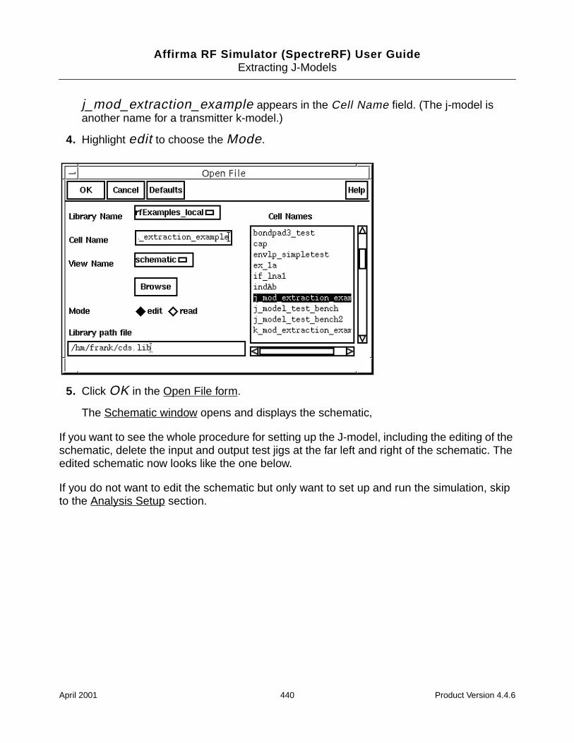
Affirma RF Simulator (SpectreRF) User GuideExtracting J-Models
j_mod_extraction_example appears in the Cell Name field. (The j-model isanother name for a transmitter k-model.)
4. Highlight edit to choose the Mode.
5. Click OK in the Open File form.
The Schematic window opens and displays the schematic,
If you want to see the whole procedure for setting up the J-model, including the editing of theschematic, delete the input and output test jigs at the far left and right of the schematic. Theedited schematic now looks like the one below.
If you do not want to edit the schematic but only want to set up and run the simulation, skipto the Analysis Setup section.
April 2001 440 Product Version 4.4.6
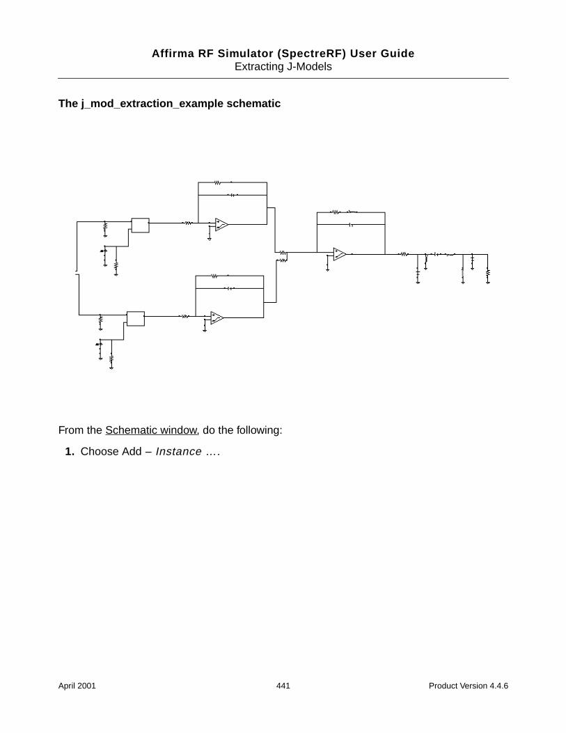
Affirma RF Simulator (SpectreRF) User GuideExtracting J-Models
The j_mod_extraction_example schematic
From the Schematic window, do the following:
1. Choose Add – Instance ….
April 2001 441 Product Version 4.4.6
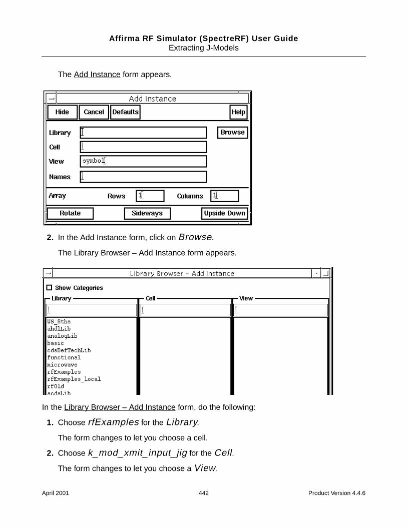
Affirma RF Simulator (SpectreRF) User GuideExtracting J-Models
The Add Instance form appears.
2. In the Add Instance form, click on Browse.
The Library Browser – Add Instance form appears.
In the Library Browser – Add Instance form, do the following:
1. Choose rfExamples for the Library.
The form changes to let you choose a cell.
2. Choose k_mod_xmit_input_jig for the Cell.
The form changes to let you choose a View.
April 2001 442 Product Version 4.4.6
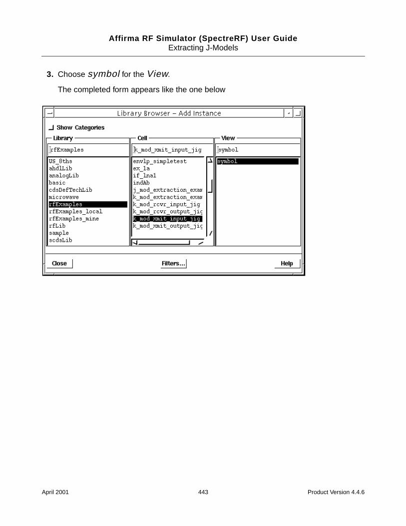
Affirma RF Simulator (SpectreRF) User GuideExtracting J-Models
3. Choose symbol for the View.
The completed form appears like the one below
April 2001 443 Product Version 4.4.6
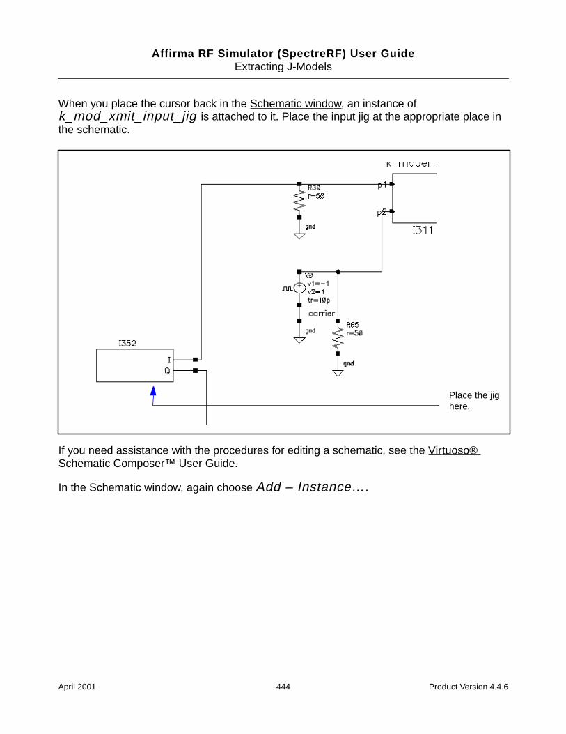
Affirma RF Simulator (SpectreRF) User GuideExtracting J-Models
When you place the cursor back in the Schematic window, an instance ofk_mod_xmit_input_jig is attached to it. Place the input jig at the appropriate place inthe schematic.
If you need assistance with the procedures for editing a schematic, see the Virtuoso®Schematic Composer™ User Guide.
In the Schematic window, again choose Add – Instance….
Place the jighere.
April 2001 444 Product Version 4.4.6
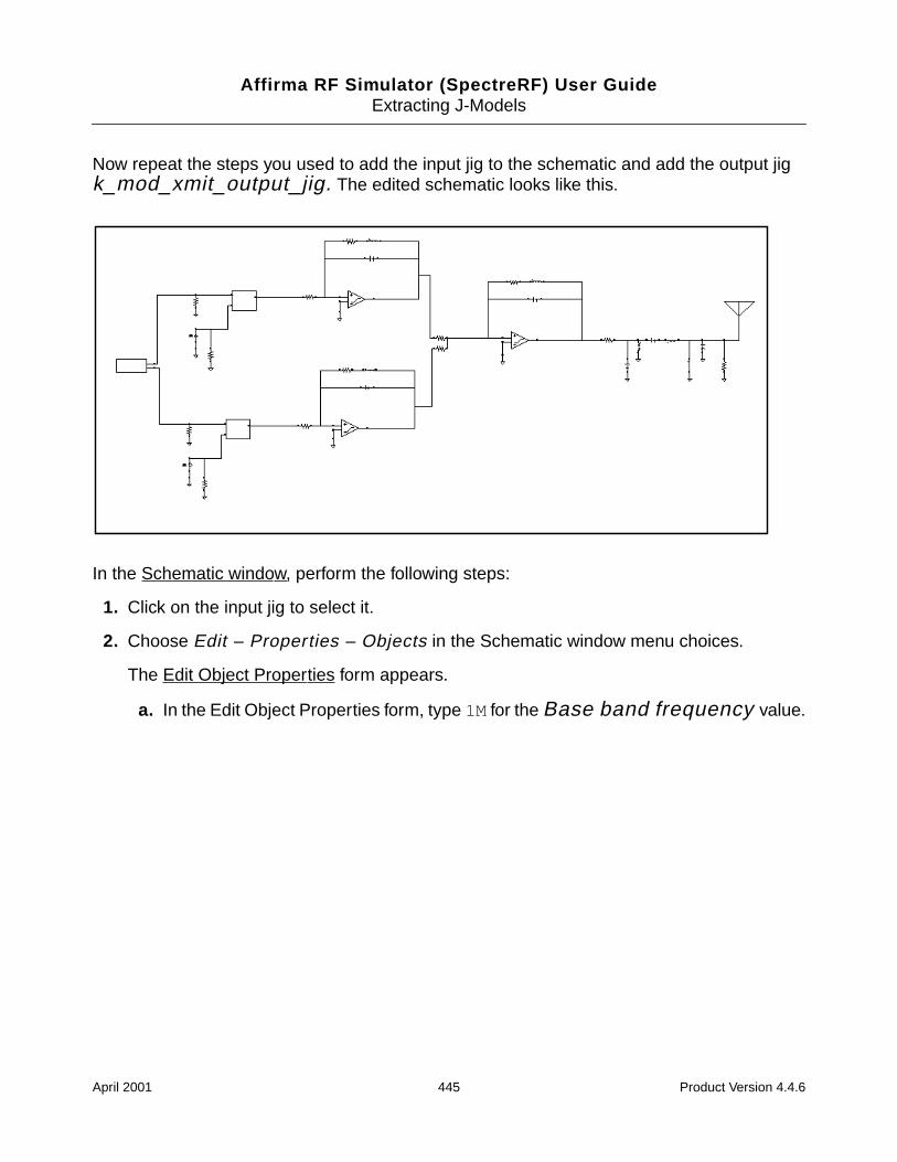
Affirma RF Simulator (SpectreRF) User GuideExtracting J-Models
Now repeat the steps you used to add the input jig to the schematic and add the output jigk_mod_xmit_output_jig. The edited schematic looks like this.
In the Schematic window, perform the following steps:
1. Click on the input jig to select it.
2. Choose Edit – Properties – Objects in the Schematic window menu choices.
The Edit Object Properties form appears.
a. In the Edit Object Properties form, type 1Mfor the Base band frequency value.
April 2001 445 Product Version 4.4.6
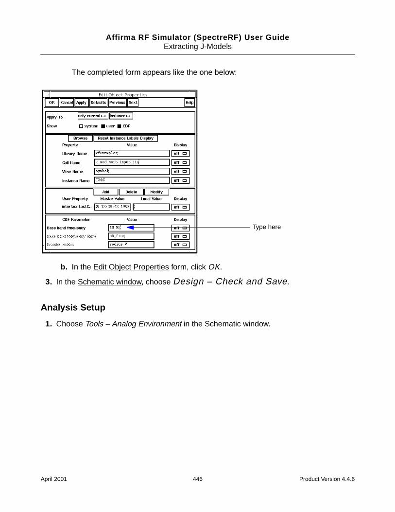
Affirma RF Simulator (SpectreRF) User GuideExtracting J-Models
The completed form appears like the one below:
b. In the Edit Object Properties form, click OK.
3. In the Schematic window, choose Design – Check and Save.
Analysis Setup
1. Choose Tools – Analog Environment in the Schematic window.
Type here
April 2001 446 Product Version 4.4.6
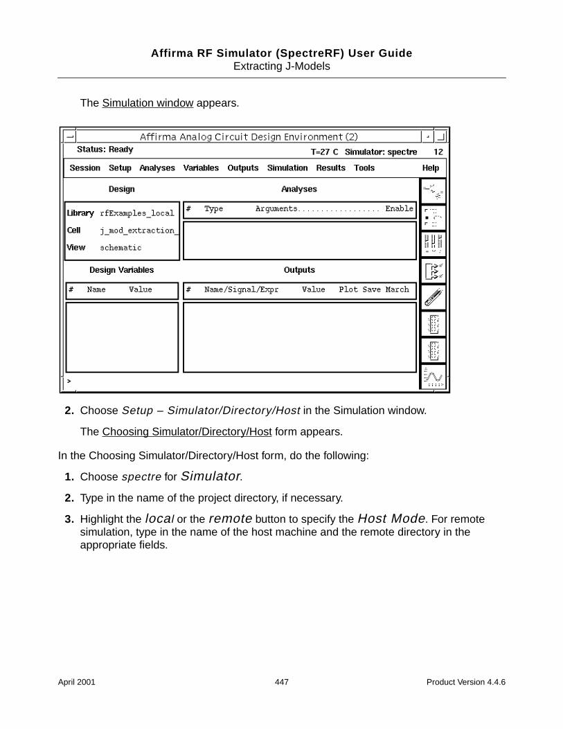
Affirma RF Simulator (SpectreRF) User GuideExtracting J-Models
The Simulation window appears.
2. Choose Setup – Simulator/Directory/Host in the Simulation window.
The Choosing Simulator/Directory/Host form appears.
In the Choosing Simulator/Directory/Host form, do the following:
1. Choose spectre for Simulator.
2. Type in the name of the project directory, if necessary.
3. Highlight the local or the remote button to specify the Host Mode. For remotesimulation, type in the name of the host machine and the remote directory in theappropriate fields.
April 2001 447 Product Version 4.4.6
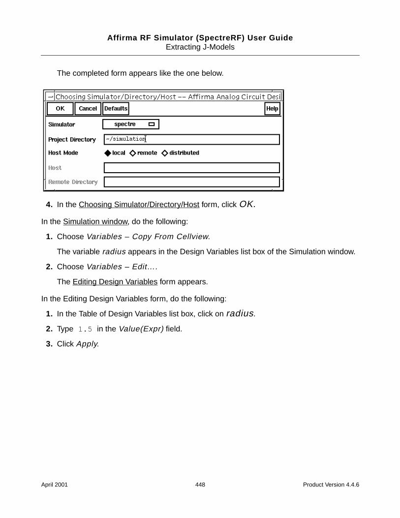
Affirma RF Simulator (SpectreRF) User GuideExtracting J-Models
The completed form appears like the one below.
4. In the Choosing Simulator/Directory/Host form, click OK.
In the Simulation window, do the following:
1. Choose Variables – Copy From Cellview.
The variable radius appears in the Design Variables list box of the Simulation window.
2. Choose Variables – Edit….
The Editing Design Variables form appears.
In the Editing Design Variables form, do the following:
1. In the Table of Design Variables list box, click on radius.
2. Type 1.5 in the Value(Expr) field.
3. Click Apply.
April 2001 448 Product Version 4.4.6
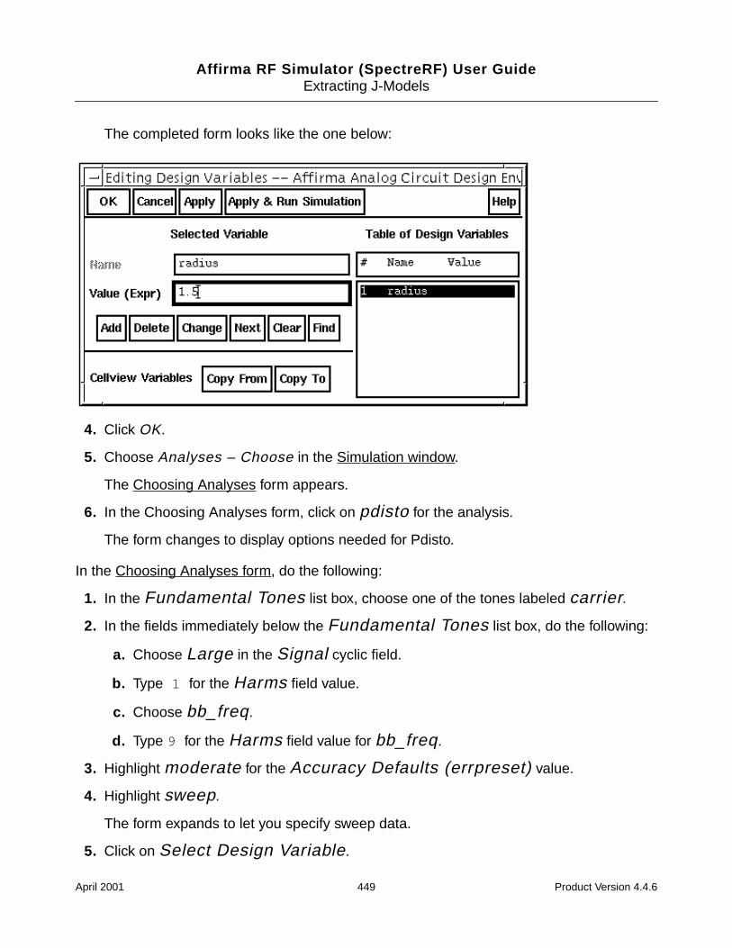
Affirma RF Simulator (SpectreRF) User GuideExtracting J-Models
The completed form looks like the one below:
4. Click OK.
5. Choose Analyses – Choose in the Simulation window.
The Choosing Analyses form appears.
6. In the Choosing Analyses form, click on pdisto for the analysis.
The form changes to display options needed for Pdisto.
In the Choosing Analyses form, do the following:
1. In the Fundamental Tones list box, choose one of the tones labeled carrier.
2. In the fields immediately below the Fundamental Tones list box, do the following:
a. Choose Large in the Signal cyclic field.
b. Type 1 for the Harms field value.
c. Choose bb_freq.
d. Type 9 for the Harms field value for bb_freq.
3. Highlight moderate for the Accuracy Defaults (errpreset) value.
4. Highlight sweep.
The form expands to let you specify sweep data.
5. Click on Select Design Variable.
April 2001 449 Product Version 4.4.6
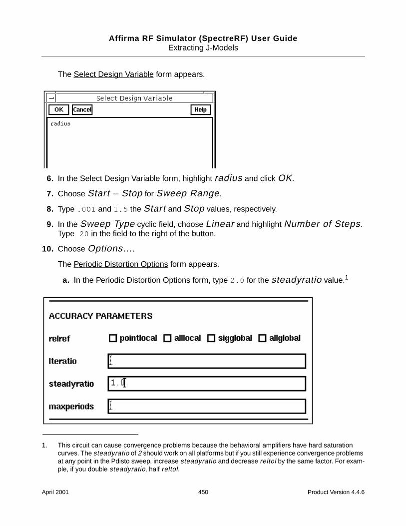
Affirma RF Simulator (SpectreRF) User GuideExtracting J-Models
The Select Design Variable form appears.
6. In the Select Design Variable form, highlight radius and click OK.
7. Choose Start – Stop for Sweep Range.
8. Type .001 and 1.5 the Start and Stop values, respectively.
9. In the Sweep Type cyclic field, choose Linear and highlight Number of Steps.Type 20 in the field to the right of the button.
10. Choose Options….
The Periodic Distortion Options form appears.
a. In the Periodic Distortion Options form, type 2.0 for the steadyratio value.1
1. This circuit can cause convergence problems because the behavioral amplifiers have hard saturationcurves. The steadyratio of 2 should work on all platforms but if you still experience convergence problemsat any point in the Pdisto sweep, increase steadyratio and decrease reltol by the same factor. For exam-ple, if you double steadyratio, half reltol.
April 2001 450 Product Version 4.4.6
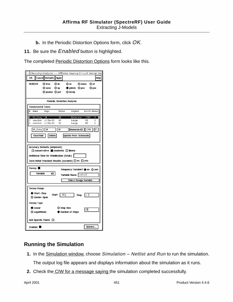
Affirma RF Simulator (SpectreRF) User GuideExtracting J-Models
b. In the Periodic Distortion Options form, click OK.
11. Be sure the Enabled button is highlighted.
The completed Periodic Distortion Options form looks like this.
Running the Simulation
1. In the Simulation window, choose Simulation – Netlist and Run to run the simulation.
The output log file appears and displays information about the simulation as it runs.
2. Check the CIW for a message saying the simulation completed successfully.
April 2001 451 Product Version 4.4.6
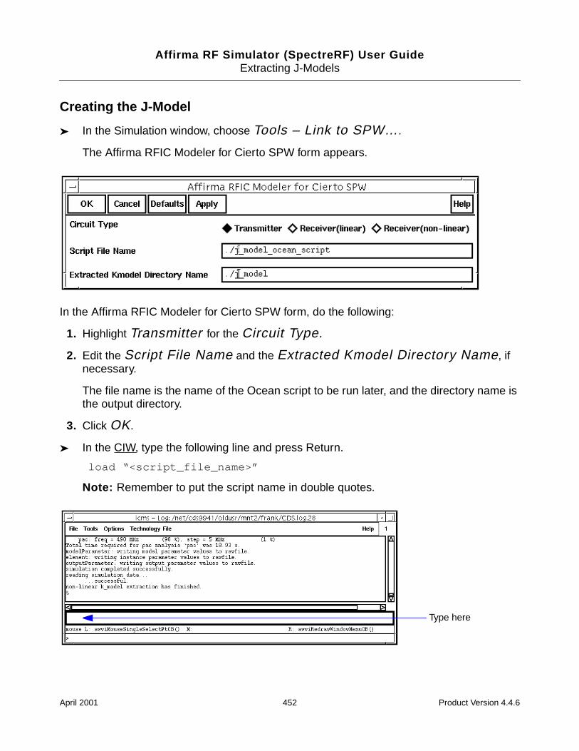
Affirma RF Simulator (SpectreRF) User GuideExtracting J-Models
Creating the J-Model
In the Simulation window, choose Tools – Link to SPW….
The Affirma RFIC Modeler for Cierto SPW form appears.
In the Affirma RFIC Modeler for Cierto SPW form, do the following:
1. Highlight Transmitter for the Circuit Type.
2. Edit the Script File Name and the Extracted Kmodel Directory Name, ifnecessary.
The file name is the name of the Ocean script to be run later, and the directory name isthe output directory.
3. Click OK.
In the CIW, type the following line and press Return.
load “<script_file_name>”
Note: Remember to put the script name in double quotes.
Type here
April 2001 452 Product Version 4.4.6
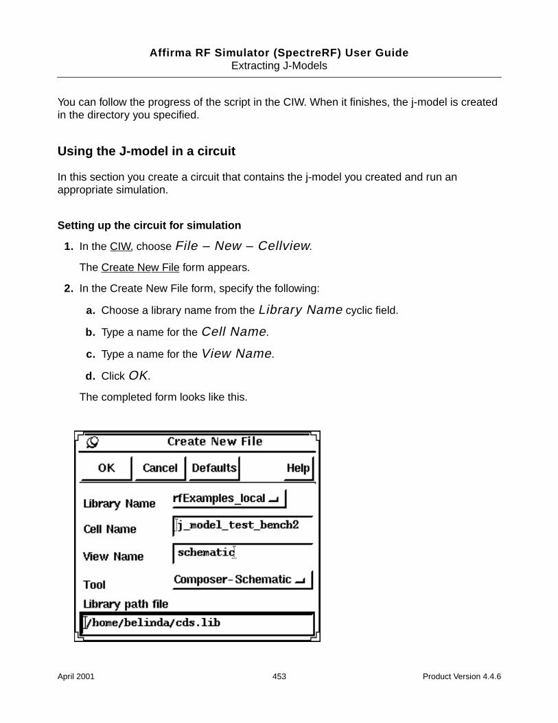
Affirma RF Simulator (SpectreRF) User GuideExtracting J-Models
You can follow the progress of the script in the CIW. When it finishes, the j-model is createdin the directory you specified.
Using the J-model in a circuit
In this section you create a circuit that contains the j-model you created and run anappropriate simulation.
Setting up the circuit for simulation
1. In the CIW, choose File – New – Cellview.
The Create New File form appears.
2. In the Create New File form, specify the following:
a. Choose a library name from the Library Name cyclic field.
b. Type a name for the Cell Name.
c. Type a name for the View Name.
d. Click OK.
The completed form looks like this.
April 2001 453 Product Version 4.4.6
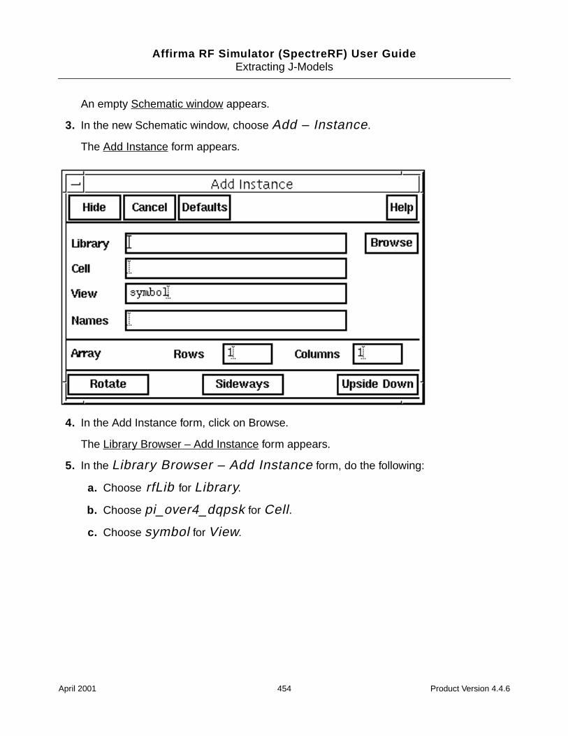
Affirma RF Simulator (SpectreRF) User GuideExtracting J-Models
An empty Schematic window appears.
3. In the new Schematic window, choose Add – Instance.
The Add Instance form appears.
4. In the Add Instance form, click on Browse.
The Library Browser – Add Instance form appears.
5. In the Library Browser – Add Instance form, do the following:
a. Choose rfLib for Library.
b. Choose pi_over4_dqpsk for Cell.
c. Choose symbol for View.
April 2001 454 Product Version 4.4.6
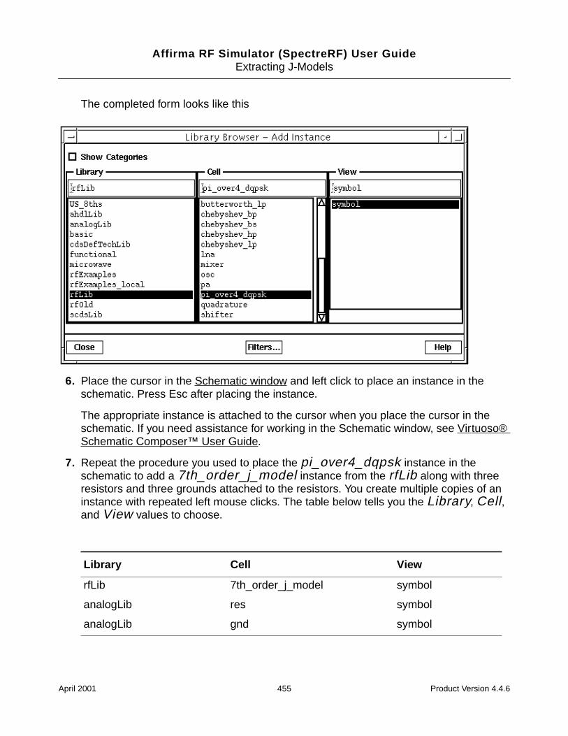
Affirma RF Simulator (SpectreRF) User GuideExtracting J-Models
The completed form looks like this
6. Place the cursor in the Schematic window and left click to place an instance in theschematic. Press Esc after placing the instance.
The appropriate instance is attached to the cursor when you place the cursor in theschematic. If you need assistance for working in the Schematic window, see Virtuoso®Schematic Composer™ User Guide.
7. Repeat the procedure you used to place the pi_over4_dqpsk instance in theschematic to add a 7th_order_j_model instance from the rfLib along with threeresistors and three grounds attached to the resistors. You create multiple copies of aninstance with repeated left mouse clicks. The table below tells you the Library, Cell,and View values to choose.
Library Cell View
rfLib 7th_order_j_model symbol
analogLib res symbol
analogLib gnd symbol
April 2001 455 Product Version 4.4.6
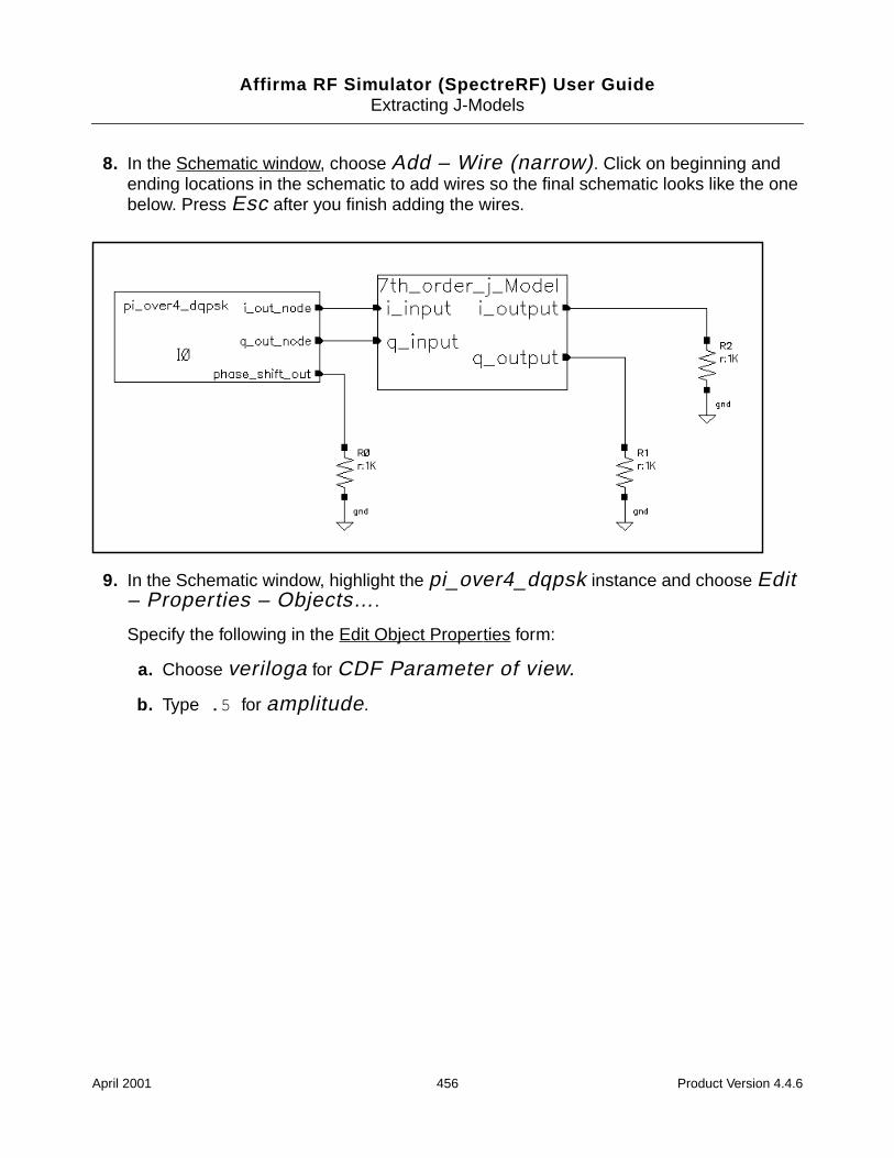
Affirma RF Simulator (SpectreRF) User GuideExtracting J-Models
8. In the Schematic window, choose Add – Wire (narrow). Click on beginning andending locations in the schematic to add wires so the final schematic looks like the onebelow. Press Esc after you finish adding the wires.
9. In the Schematic window, highlight the pi_over4_dqpsk instance and choose Edit– Properties – Objects….
Specify the following in the Edit Object Properties form:
a. Choose veriloga for CDF Parameter of view.
b. Type .5 for amplitude.
April 2001 456 Product Version 4.4.6
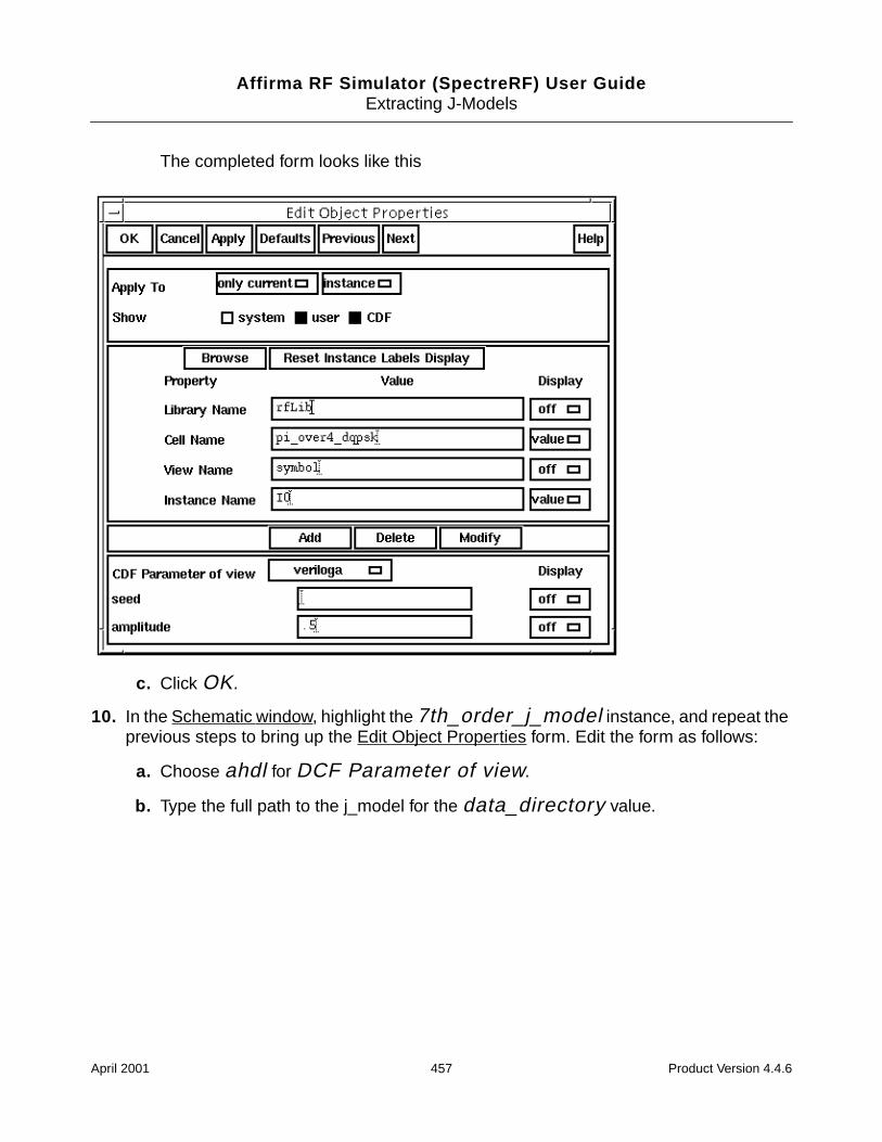
Affirma RF Simulator (SpectreRF) User GuideExtracting J-Models
The completed form looks like this
c. Click OK.
10. In the Schematic window, highlight the 7th_order_j_model instance, and repeat theprevious steps to bring up the Edit Object Properties form. Edit the form as follows:
a. Choose ahdl for DCF Parameter of view.
b. Type the full path to the j_model for the data_directory value.
April 2001 457 Product Version 4.4.6
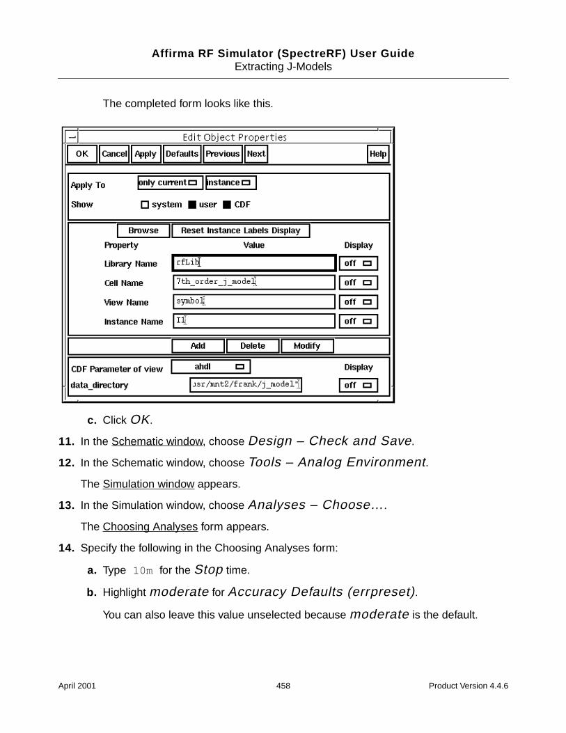
Affirma RF Simulator (SpectreRF) User GuideExtracting J-Models
The completed form looks like this.
c. Click OK.
11. In the Schematic window, choose Design – Check and Save.
12. In the Schematic window, choose Tools – Analog Environment.
The Simulation window appears.
13. In the Simulation window, choose Analyses – Choose….
The Choosing Analyses form appears.
14. Specify the following in the Choosing Analyses form:
a. Type 10m for the Stop time.
b. Highlight moderate for Accuracy Defaults (errpreset).
You can also leave this value unselected because moderate is the default.
April 2001 458 Product Version 4.4.6
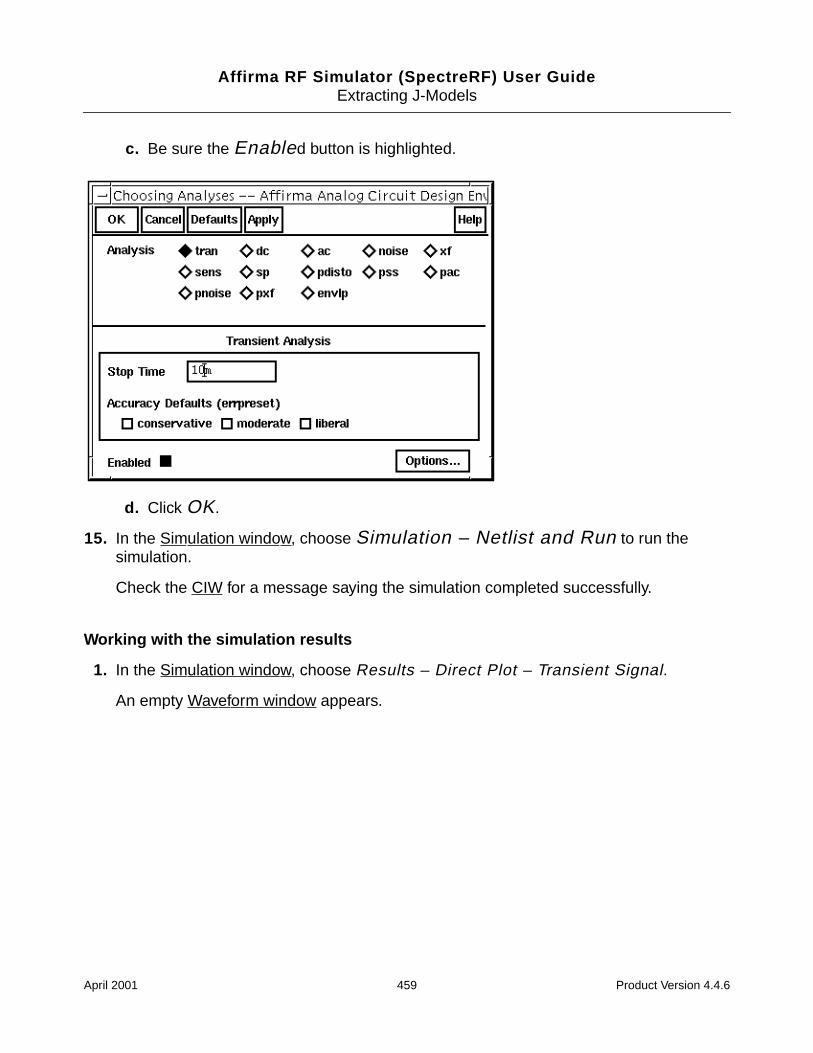
Affirma RF Simulator (SpectreRF) User GuideExtracting J-Models
c. Be sure the Enabled button is highlighted.
d. Click OK.
15. In the Simulation window, choose Simulation – Netlist and Run to run thesimulation.
Check the CIW for a message saying the simulation completed successfully.
Working with the simulation results
1. In the Simulation window, choose Results – Direct Plot – Transient Signal.
An empty Waveform window appears.
April 2001 459 Product Version 4.4.6
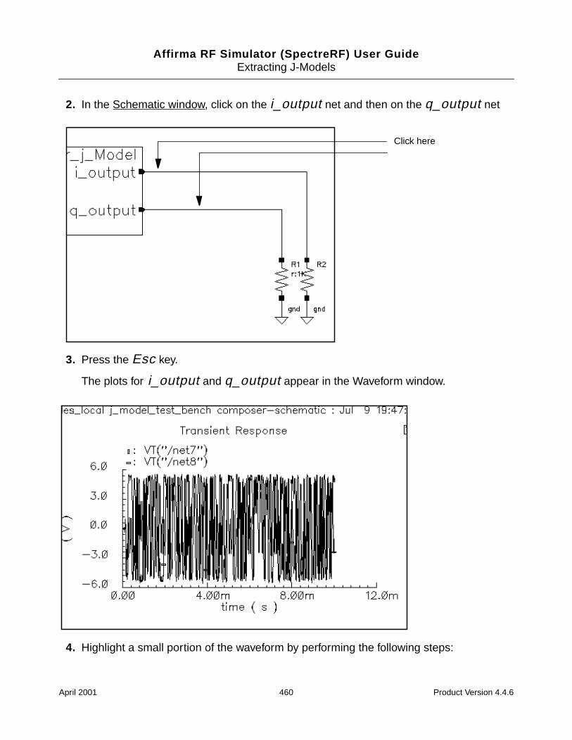
Affirma RF Simulator (SpectreRF) User GuideExtracting J-Models
2. In the Schematic window, click on the i_output net and then on the q_output net
3. Press the Esc key.
The plots for i_output and q_output appear in the Waveform window.
4. Highlight a small portion of the waveform by performing the following steps:
Click here
April 2001 460 Product Version 4.4.6
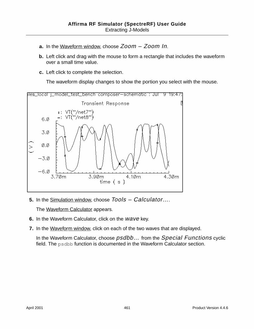
Affirma RF Simulator (SpectreRF) User GuideExtracting J-Models
a. In the Waveform window, choose Zoom – Zoom In.
b. Left click and drag with the mouse to form a rectangle that includes the waveformover a small time value.
c. Left click to complete the selection.
The waveform display changes to show the portion you select with the mouse.
5. In the Simulation window, choose Tools – Calculator….
The Waveform Calculator appears.
6. In the Waveform Calculator, click on the wave key.
7. In the Waveform window, click on each of the two waves that are displayed.
In the Waveform Calculator, choose psdbb… from the Special Functions cyclicfield. The psdbb function is documented in the Waveform Calculator section.
April 2001 461 Product Version 4.4.6
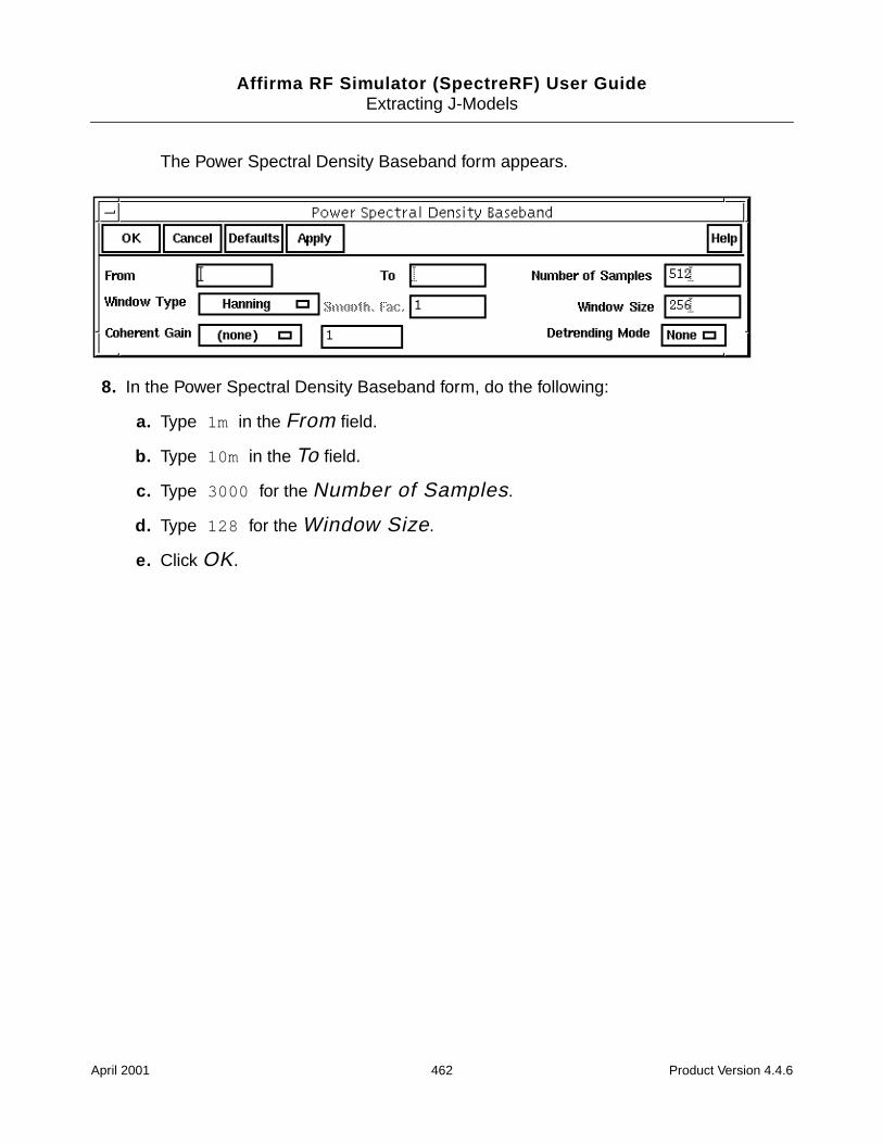
Affirma RF Simulator (SpectreRF) User GuideExtracting J-Models
The Power Spectral Density Baseband form appears.
8. In the Power Spectral Density Baseband form, do the following:
a. Type 1m in the From field.
b. Type 10m in the To field.
c. Type 3000 for the Number of Samples.
d. Type 128 for the Window Size.
e. Click OK.
April 2001 462 Product Version 4.4.6
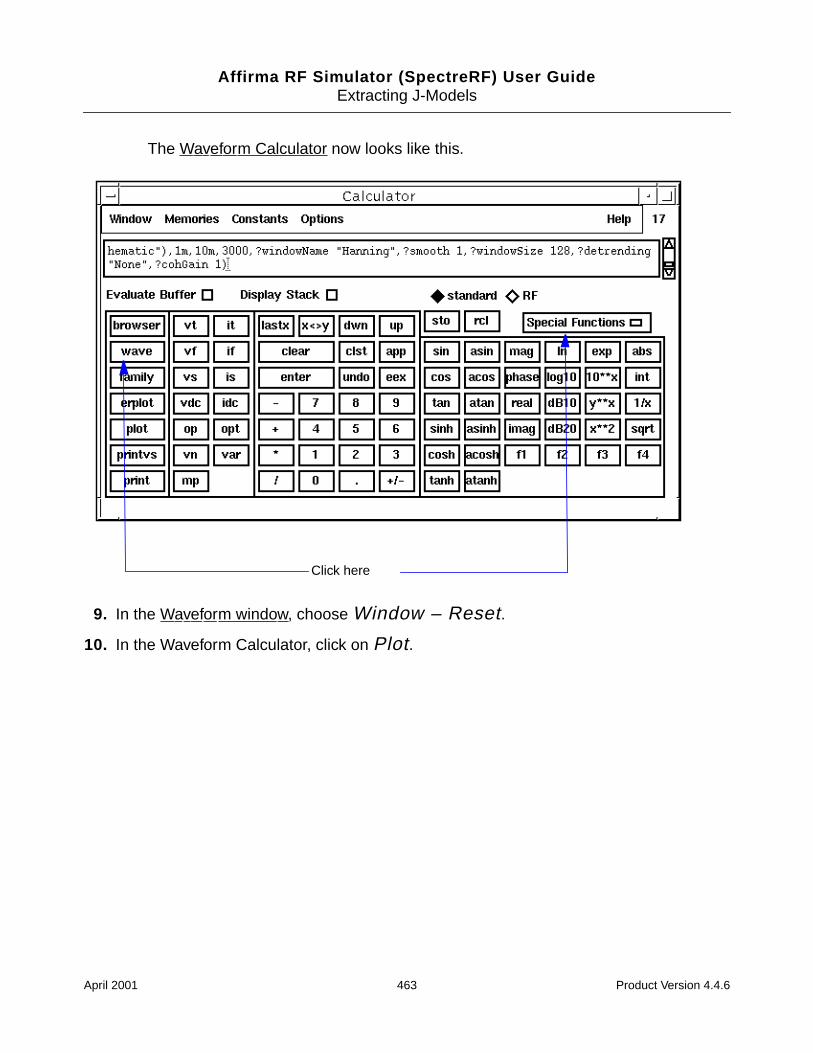
Affirma RF Simulator (SpectreRF) User GuideExtracting J-Models
The Waveform Calculator now looks like this.
9. In the Waveform window, choose Window – Reset.
10. In the Waveform Calculator, click on Plot.
Click here
April 2001 463 Product Version 4.4.6
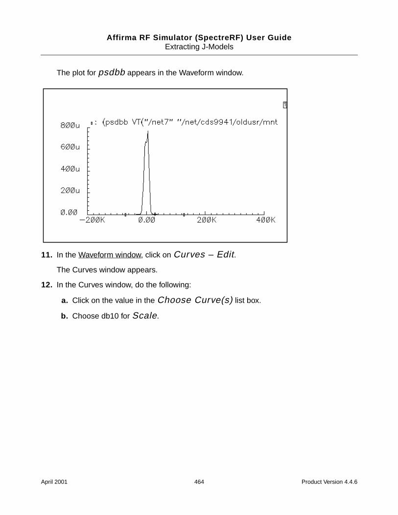
Affirma RF Simulator (SpectreRF) User GuideExtracting J-Models
The plot for psdbb appears in the Waveform window.
11. In the Waveform window, click on Curves – Edit.
The Curves window appears.
12. In the Curves window, do the following:
a. Click on the value in the Choose Curve(s) list box.
b. Choose db10 for Scale.
April 2001 464 Product Version 4.4.6
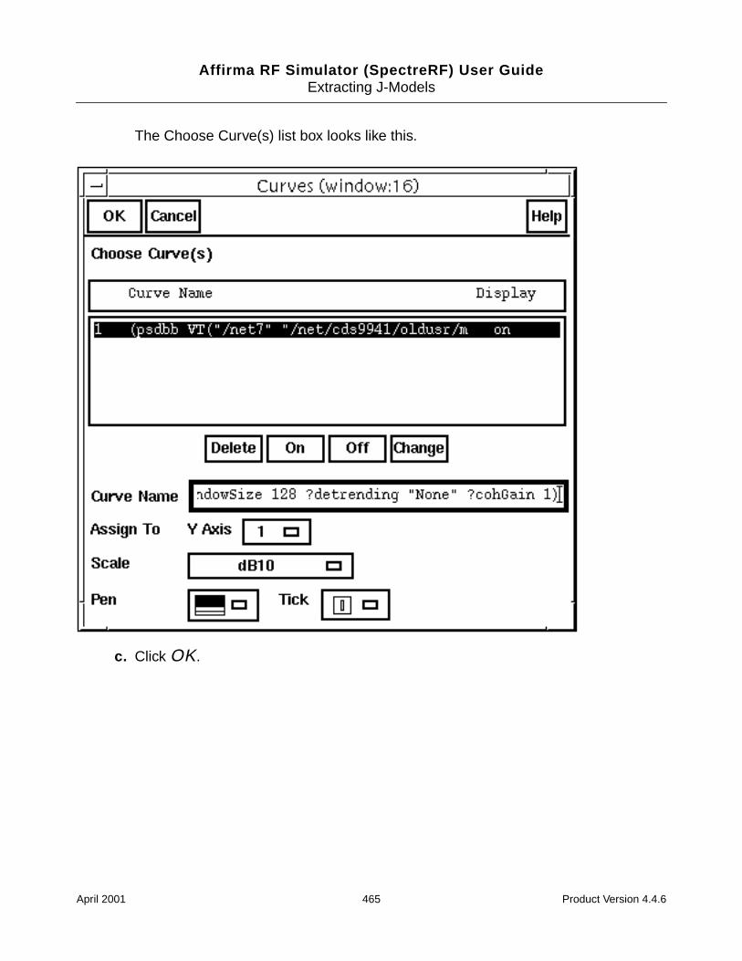
Affirma RF Simulator (SpectreRF) User GuideExtracting J-Models
The Choose Curve(s) list box looks like this.
c. Click OK.
April 2001 465 Product Version 4.4.6
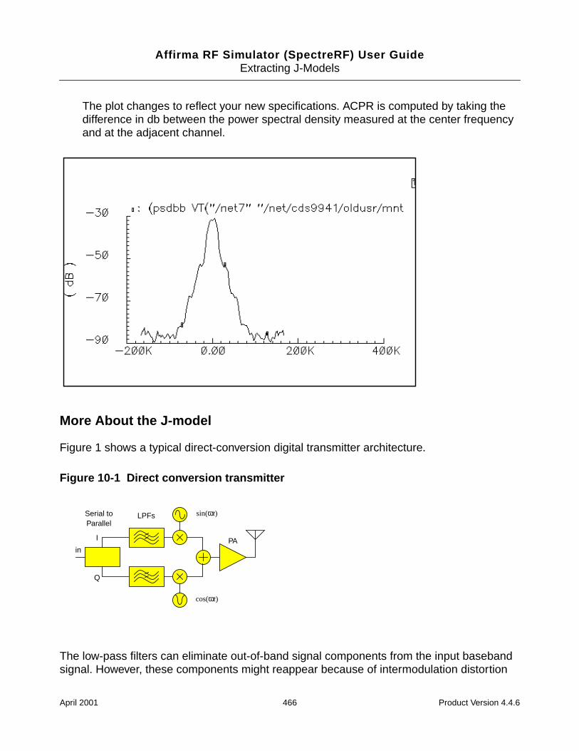
Affirma RF Simulator (SpectreRF) User GuideExtracting J-Models
The plot changes to reflect your new specifications. ACPR is computed by taking thedifference in db between the power spectral density measured at the center frequencyand at the adjacent channel.
More About the J-model
Figure 1 shows a typical direct-conversion digital transmitter architecture.
Figure 10-1 Direct conversion transmitter
The low-pass filters can eliminate out-of-band signal components from the input basebandsignal. However, these components might reappear because of intermodulation distortion
Serial toParallel
LPFs
PA
sin(ωt)
cos(ωt)
in
I
Q
April 2001 466 Product Version 4.4.6
Affirma RF Simulator (SpectreRF) User GuideExtracting J-Models
generated within the transmitter, such as in the downstream power amplifier. This return ofunwanted signal components is called “spectral regrowth.”
Adjacent Channel Power Ratio (ACPR) is a popular measure of spectral regrowth in digitaltransmitters and is often a design specification. To get the frequency resolution required foraccurate estimation of ACPR, the simulation often must process a random sequence ofbetween 500 and 10k input symbols.
Envelope Following simulates the transmitter efficiently, but it must be driven by deterministicor unfiltered random signals, and a simulation of 10k signals is lengthy.
Most filters, like those in Figure 1, are FIR filters. SpectreRF does not work with FIR filters(implemented in AHDL) because they contain hidden state. To drive an Envelope Followinganalysis with realistic random baseband signals, you must create the signals in a separatesimulation, store them to a file, then read the data into the Envelope Following analysis withpiece-wise linear sources. However, the Pdisto analysis can perform a fast, indirect ACPRestimation that can simulate 10k symbols within minutes after you extract the model.Extraction time is independent of the number of symbols you want to simulate.
Initially, Pdisto extracts a behavioral baseband-equivalent model of the transmitter. Intransmitter circuits, the input baseband signal is usually well within the transmitter’sbandwidth, so a model without memory, such as the J-model, is often sufficient. Because thebehavioral model eliminates the carrier and unnecessary circuit details, the subsequentACPR calculation step is fast, even for large or complex circuits.
The most familiar spectral regrowth mechanism is the intermodulation distortion of amplitudemodulation (AM) signal components that enter the power amplifier. Modulation schemes thatcarry information only on the carrier phase or frequency try to minimize spectral regrowth byeliminating this AM component. However, the digital baseband filters can still convertdiscontinuous phase changes into amplitude transients in the composite RF signal. Modelsbased on AM/AM and AM/PM conversion [2] capture most such power amplifier relateddistortion mechanisms. However, imperfections in the I/Q modulators can convert inputphase variations into output amplitude and phase variations that also contribute to thedistortion. This is particularly true for GSM transmitters. For this reason, we also include PM/AM and PM/PM conversion effects in our model. Formally, the J-model is a narrowbandapproximation to a vector-valued, periodically time-varying, functional series expansion [3].
To understand the extraction procedure, write the inputs in polar coordinates, such asmagnitude ρ and phase φ. Consider the mapping f(ρ,φ) from baseband input to the basebandrepresentation of the RF output. That is, if
,input ρ φ( )cos jρ φ( )sin+=
April 2001 467 Product Version 4.4.6
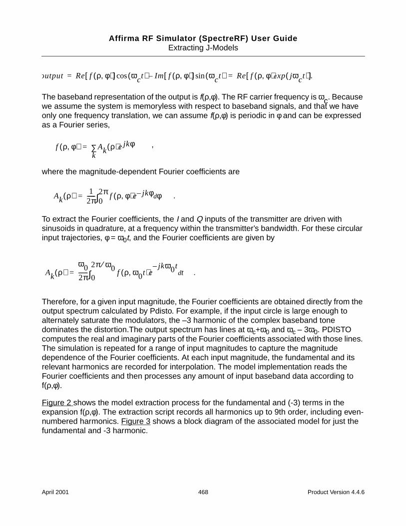
Affirma RF Simulator (SpectreRF) User GuideExtracting J-Models
.
The baseband representation of the output is f(ρ,φ). The RF carrier frequency is ωc. Becausewe assume the system is memoryless with respect to baseband signals, and that we haveonly one frequency translation, we can assume f(ρ,φ) is periodic in φ and can be expressedas a Fourier series,
,
where the magnitude-dependent Fourier coefficients are
.
To extract the Fourier coefficients, the I and Q inputs of the transmitter are driven withsinusoids in quadrature, at a frequency within the transmitter’s bandwidth. For these circularinput trajectories, φ = ω0t, and the Fourier coefficients are given by
.
Therefore, for a given input magnitude, the Fourier coefficients are obtained directly from theoutput spectrum calculated by Pdisto. For example, if the input circle is large enough toalternately saturate the modulators, the –3 harmonic of the complex baseband tonedominates the distortion.The output spectrum has lines at ωc+ω0 and ωc – 3ω0. PDISTOcomputes the real and imaginary parts of the Fourier coefficients associated with those lines.The simulation is repeated for a range of input magnitudes to capture the magnitudedependence of the Fourier coefficients. At each input magnitude, the fundamental and itsrelevant harmonics are recorded for interpolation. The model implementation reads theFourier coefficients and then processes any amount of input baseband data according tof(ρ,φ).
Figure 2 shows the model extraction process for the fundamental and (-3) terms in theexpansion f(ρ,φ). The extraction script records all harmonics up to 9th order, including even-numbered harmonics. Figure 3 shows a block diagram of the associated model for just thefundamental and -3 harmonic.
output Re f ρ φ,( )[ ] ωct( )cos Im f ρ φ,( )[ ] ωct( )sin– Re f ρ φ,( )exp jωct( )[ ]= =
f ρ φ,( ) Ak ρ( )ejkφk∑=
Ak ρ( ) 12π------ f ρ φ,( )e j– kφ φd
02π
∫=
Ak ρ( )ω02π------- f ρ ω0t,( )e
j– kω0ttd
0
2π ω0⁄∫=
April 2001 468 Product Version 4.4.6
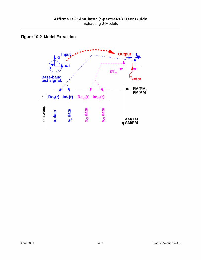
Affirma RF Simulator (SpectreRF) User GuideExtracting J-Models
Figure 10-2 Model Extraction
fcarrier
fm
3*fm
i
q
Base-bandtest signal.
Output
r
r Re1(r) Im1(r) Re-3(r) Im-3(r)
r -
swee
p
x 1da
ta
y 1 d
ata
x -3
data
y -3
data
Input
PM/PM,
AM/AMAM/PM
PM/AM
April 2001 469 Product Version 4.4.6
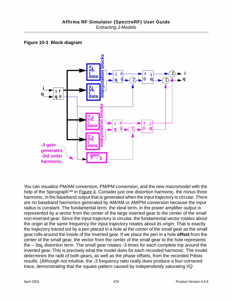
Affirma RF Simulator (SpectreRF) User GuideExtracting J-Models
Figure 10-3 Block diagram
You can visualize PM/AM conversion, PM/PM conversion, and the new macromodel with thehelp of the Spirograph™ in Figure 4. Consider just one distortion harmonic, the minus threeharmonic, in the baseband output that is generated when the input trajectory is circular. Thereare no baseband harmonics generated by AM/AM or AM/PM conversion because the inputradius is constant. The fundamental term. the ideal term, in the power amplifier output isrepresented by a vector from the center of the large inverted gear to the center of the smallnon-inverted gear. Since the input trajectory is circular, the fundamental vector rotates aboutthe origin at the same frequency the input trajectory rotates about its origin. That is exactlythe trajectory traced out by a pen placed in a hole at the center of the small gear as the smallgear rolls around the inside of the inverted gear. If we place the pen in a hole offset from thecenter of the small gear, the vector from the center of the small gear to the hole representsthe – 3ω0 distortion term. The small gear rotates -3 times for each complete trip around theinverted gear. This is precisely what the model does for each recorded harmonic. The modeldetermines the radii of both gears, as well as the phase offsets, from the recorded Pdistoresults. (Although not intuitive, the -3 frequency ratio really does produce a four-corneredtrace, demonstrating that the square pattern caused by independently saturating I/Q
iq
iq
rθ
iq
x1
y1iq
ΣΣθ
r
θr
vs.rdata
vs.rdata In
terp
olat
ion
bloc
ks
Σ
iq
rθ
iq
x-3
y-3
θr
vs.rdata
vs.rdata In
terp
olat
ion
bloc
ks
Σ
gain= - 3
iq
-3 gaingenerates-3rd orderharmonic.
April 2001 470 Product Version 4.4.6
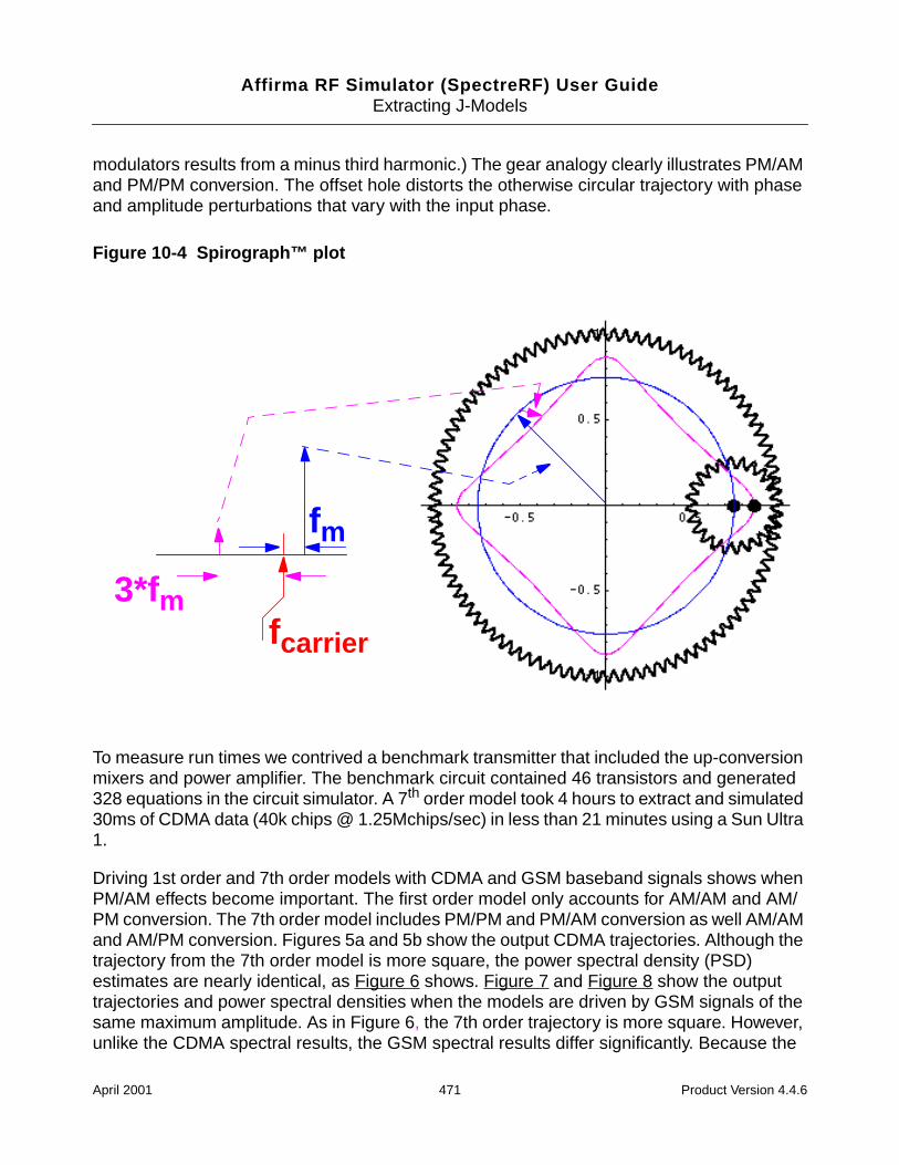
Affirma RF Simulator (SpectreRF) User GuideExtracting J-Models
modulators results from a minus third harmonic.) The gear analogy clearly illustrates PM/AMand PM/PM conversion. The offset hole distorts the otherwise circular trajectory with phaseand amplitude perturbations that vary with the input phase.
Figure 10-4 Spirograph™ plot
To measure run times we contrived a benchmark transmitter that included the up-conversionmixers and power amplifier. The benchmark circuit contained 46 transistors and generated328 equations in the circuit simulator. A 7th order model took 4 hours to extract and simulated30ms of CDMA data (40k chips @ 1.25Mchips/sec) in less than 21 minutes using a Sun Ultra1.
Driving 1st order and 7th order models with CDMA and GSM baseband signals shows whenPM/AM effects become important. The first order model only accounts for AM/AM and AM/PM conversion. The 7th order model includes PM/PM and PM/AM conversion as well AM/AMand AM/PM conversion. Figures 5a and 5b show the output CDMA trajectories. Although thetrajectory from the 7th order model is more square, the power spectral density (PSD)estimates are nearly identical, as Figure 6 shows. Figure 7 and Figure 8 show the outputtrajectories and power spectral densities when the models are driven by GSM signals of thesame maximum amplitude. As in Figure 6, the 7th order trajectory is more square. However,unlike the CDMA spectral results, the GSM spectral results differ significantly. Because the
fcarrier
fm
3*fm
April 2001 471 Product Version 4.4.6
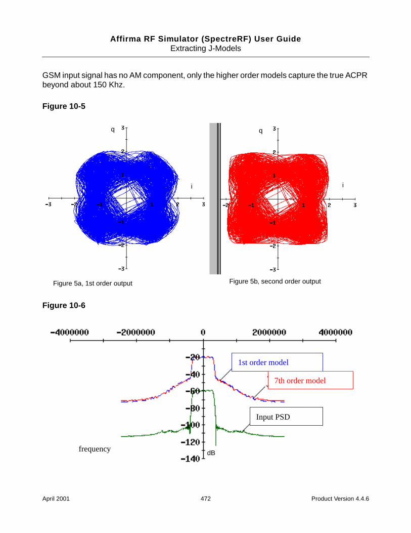
Affirma RF Simulator (SpectreRF) User GuideExtracting J-Models
GSM input signal has no AM component, only the higher order models capture the true ACPRbeyond about 150 Khz.
Figure 10-5
Figure 10-6
Figure 5a, 1st order output Figure 5b, second order output
q q
i i
frequency
1st order model
7th order model
Input PSD
dB
April 2001 472 Product Version 4.4.6
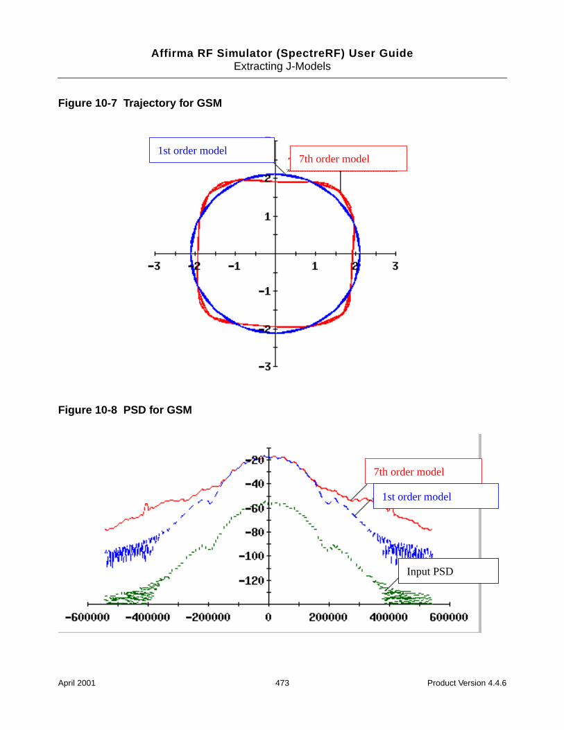
Affirma RF Simulator (SpectreRF) User GuideExtracting J-Models
Figure 10-7 Trajectory for GSM
Figure 10-8 PSD for GSM
1st order model7th order model
Input PSD
7th order model
1st order model
April 2001 473 Product Version 4.4.6
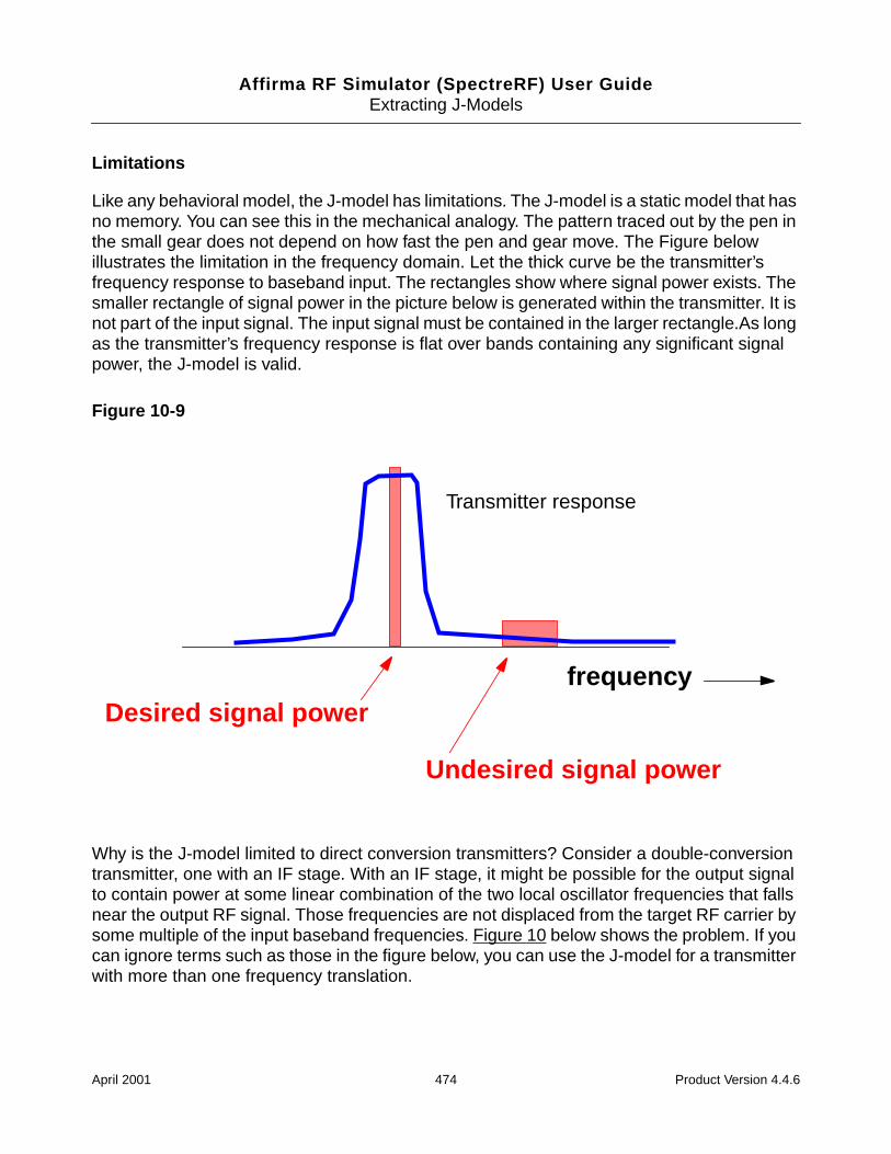
Affirma RF Simulator (SpectreRF) User GuideExtracting J-Models
Limitations
Like any behavioral model, the J-model has limitations. The J-model is a static model that hasno memory. You can see this in the mechanical analogy. The pattern traced out by the pen inthe small gear does not depend on how fast the pen and gear move. The Figure belowillustrates the limitation in the frequency domain. Let the thick curve be the transmitter’sfrequency response to baseband input. The rectangles show where signal power exists. Thesmaller rectangle of signal power in the picture below is generated within the transmitter. It isnot part of the input signal. The input signal must be contained in the larger rectangle.As longas the transmitter’s frequency response is flat over bands containing any significant signalpower, the J-model is valid.
Figure 10-9
Why is the J-model limited to direct conversion transmitters? Consider a double-conversiontransmitter, one with an IF stage. With an IF stage, it might be possible for the output signalto contain power at some linear combination of the two local oscillator frequencies that fallsnear the output RF signal. Those frequencies are not displaced from the target RF carrier bysome multiple of the input baseband frequencies. Figure 10 below shows the problem. If youcan ignore terms such as those in the figure below, you can use the J-model for a transmitterwith more than one frequency translation.
frequencyDesired signal power
Undesired signal power
Transmitter response
April 2001 474 Product Version 4.4.6
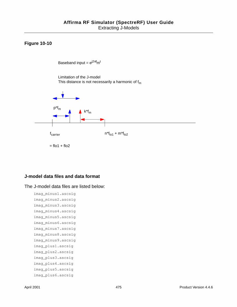
Affirma RF Simulator (SpectreRF) User GuideExtracting J-Models
Figure 10-10
J-model data files and data format
The J-model data files are listed below:
imag_minus1.ascsig
imag_minus2.ascsig
imag_minus3.ascsig
imag_minus4.ascsig
imag_minus5.ascsig
imag_minus6.ascsig
imag_minus7.ascsig
imag_minus8.ascsig
imag_minus9.ascsig
imag_plus1.ascsig
imag_plus2.ascsig
imag_plus3.ascsig
imag_plus4.ascsig
imag_plus5.ascsig
imag_plus6.ascsig
Baseband input = ej2πfmt
Limitation of the J-modelThis distance is not necessarily a harmonic of fm
p*fmk*fm
n*flo1 + m*flo2fcarrier
= flo1 + flo2
April 2001 475 Product Version 4.4.6
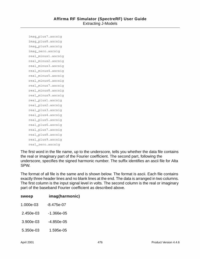
Affirma RF Simulator (SpectreRF) User GuideExtracting J-Models
imag_plus7.ascsig
imag_plus8.ascsig
imag_plus9.ascsig
imag_zero.ascsig
real_minus1.ascsig
real_minus2.ascsig
real_minus3.ascsig
real_minus4.ascsig
real_minus5.ascsig
real_minus6.ascsig
real_minus7.ascsig
real_minus8.ascsig
real_minus9.ascsig
real_plus1.ascsig
real_plus2.ascsig
real_plus3.ascsig
real_plus4.ascsig
real_plus5.ascsig
real_plus6.ascsig
real_plus7.ascsig
real_plus8.ascsig
real_plus9.ascsig
real_zero.ascsig
The first word in the file name, up to the underscore, tells you whether the data file containsthe real or imaginary part of the Fourier coefficient. The second part, following theunderscore, specifies the signed harmonic number. The suffix identifies an ascii file for AltaSPW.
The format of all file is the same and is shown below. The format is ascii. Each file containsexactly three header lines and no blank lines at the end. The data is arranged in two columns.The first column is the input signal level in volts. The second column is the real or imaginarypart of the baseband Fourier coefficient as described above.
sweep imag(harmonic)
1.000e-03 -8.475e-07
2.450e-03 -1.366e-05
3.900e-03 -4.850e-05
5.350e-03 1.595e-05
April 2001 476 Product Version 4.4.6
Affirma RF Simulator (SpectreRF) User GuideExtracting J-Models
6.800e-03 3.690e-05
8.250e-03 -7.153e-04
9.700e-03 -1.055e-04
1.115e-02 -4.324e-05
1.260e-02 -1.431e-04
1.405e-02 -1.143e-03
1.550e-02 -4.352e-03
1.695e-02 -5.443e-04
1.840e-02 1.107e-03
1.985e-02 1.913e-03
2.130e-02 3.774e-02
2.275e-02 8.256e-02
2.420e-02 1.277e-01
2.565e-02 1.680e-01
2.710e-02 2.114e-01
2.855e-02 2.474e-01
3.000e-02 2.841e-01
References
[1] E. Ngoya and R. Larcheveque. Envelope transient analysis: a new method for the transientand steady state analysis of microwave communication circuits and systems. IEEE MTTSymposium Digest, pp. 1365-1368, June 1996.
[2] M. Jeruchim, P. Balaban and K. Shanmugan, Simulation of Communication Systems,Plenum, 1992.
[3] M. Schetzen, “The Volterra & Wiener Theories of Non-Linear Systems”, Krieger PublishingCompany, 1980.
April 2001 477 Product Version 4.4.6
Affirma RF Simulator (SpectreRF) User Guide
11Modeling Transmitters
This chapter tells you how to use several of the new SpectreRF features to designtransmitters. It particularly emphasizes
Running an Envelope Following analysis
Measuring Load Pull Contours and Reflection Coefficients
Using S-parameter Input Files
The Envelope Following example explains
How to interpret the analysis results
How to quickly detect distortion visually
How to compute the transmitted power spectral density. ACPR (Adjacent Channel PowerRatio) is the number that characterizes transmitter power spectral densities.
The Load-Pull example explains how to select an optimal power amplifier load and determinewhether the input matching network needs to be re-designed for the optimal load.
The S-parameter example explains how to generate tabulated S-parameters and includethem as input in a SpectreRF analysis.
Envelope Following
This example tells you how to set up and run the Envelope Following analysis then explainswhy the time results look somewhat unusual.
Before you start, perform the setup procedures described in Chapter 3.
1. In the CIW, choose File – Open….
April 2001 478 Product Version 4.4.6
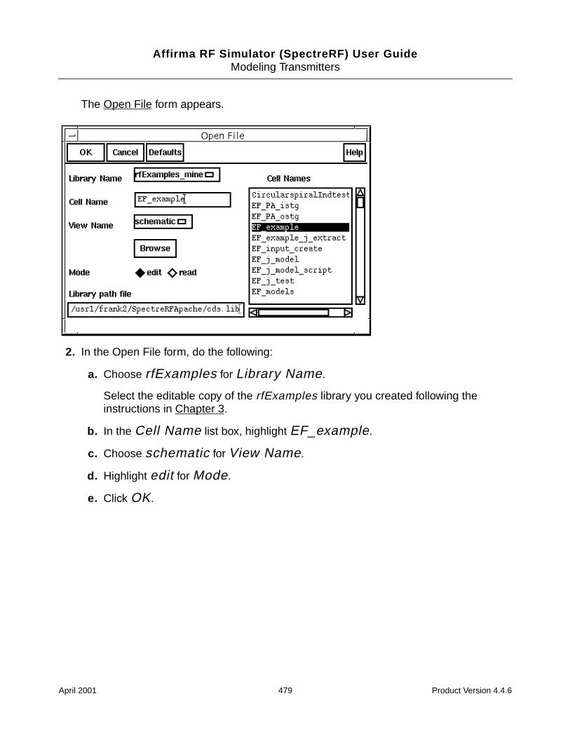
Affirma RF Simulator (SpectreRF) User GuideModeling Transmitters
The Open File form appears.
2. In the Open File form, do the following:
a. Choose rfExamples for Library Name.
Select the editable copy of the rfExamples library you created following theinstructions in Chapter 3.
b. In the Cell Name list box, highlight EF_example.
c. Choose schematic for View Name.
d. Highlight edit for Mode.
e. Click OK.
April 2001 479 Product Version 4.4.6

Affirma RF Simulator (SpectreRF) User GuideModeling Transmitters
The Schematic window appears with the EF_example schematic. This is a simpledirect-conversion transmitter with ideal I/Q modulators.
3. In the Schematic window, choose Tools – Analog Environment.
The Simulation window appears.
April 2001 480 Product Version 4.4.6
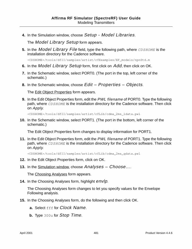
Affirma RF Simulator (SpectreRF) User GuideModeling Transmitters
4. In the Simulation window, choose Setup - Model Libraries.
The Model Library Setup form appears.
5. In the Model Library File field, type the following path, where CDSHOME is theinstallation directory for the Cadence software.
<CDSHOME>/tools/dfII/samples/artist/rfExamples/EF_models/npnStd.m
6. In the Model Library Setup form, first click on Add, then click on OK.
7. In the Schematic window, select PORT0. (The port in the top, left corner of theschematic.)
8. In the Schematic window, choose Edit – Properties – Objects.
The Edit Object Properties form appears.
9. In the Edit Object Properties form, edit the PWL filename of PORT0. Type the followingpath, where CDSHOMEis the installation directory for the Cadence software. Then clickon Apply.
<CDSHOME>/tools/dfII/samples/artist/rfLib/cdma_2ms_idata.pwl
10. In the Schematic window, select PORT1. (The port in the bottom, left corner of theschematic.)
The Edit Object Properties form changes to display information for PORT1.
11. In the Edit Object Properties form, edit the PWL filename of PORT1. Type the followingpath, where CDSHOMEis the installation directory for the Cadence software. Then clickon Apply.
<CDSHOME>/tools/dfII/samples/artist/rfLib/cdma_2ms_qdata.pwl
12. In the Edit Object Properties form, click on OK.
13. In the Simulation window, choose Analyses – Choose….
The Choosing Analyses form appears.
14. In the Choosing Analyses form, highlight envlp.
The Choosing Analyses form changes to let you specify values for the EnvelopeFollowing analysis.
15. In the Choosing Analyses form, do the following and then click OK.
a. Select fff for Clock Name.
b. Type 300u for Stop Time.
April 2001 481 Product Version 4.4.6
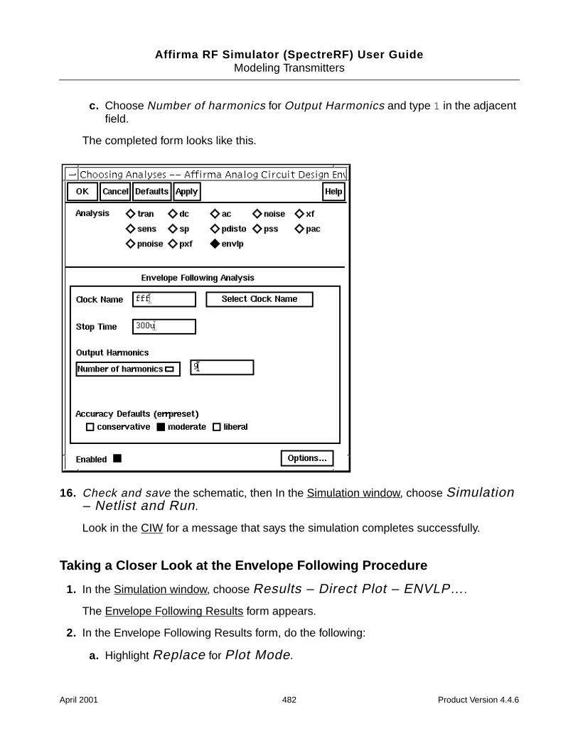
Affirma RF Simulator (SpectreRF) User GuideModeling Transmitters
c. Choose Number of harmonics for Output Harmonics and type 1 in the adjacentfield.
The completed form looks like this.
16. Check and save the schematic, then In the Simulation window, choose Simulation– Netlist and Run.
Look in the CIW for a message that says the simulation completes successfully.
Taking a Closer Look at the Envelope Following Procedure
1. In the Simulation window, choose Results – Direct Plot – ENVLP….
The Envelope Following Results form appears.
2. In the Envelope Following Results form, do the following:
a. Highlight Replace for Plot Mode.
April 2001 482 Product Version 4.4.6
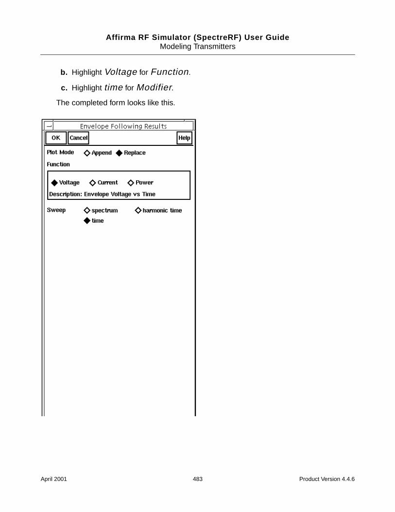
Affirma RF Simulator (SpectreRF) User GuideModeling Transmitters
b. Highlight Voltage for Function.
c. Highlight time for Modifier.
The completed form looks like this.
April 2001 483 Product Version 4.4.6
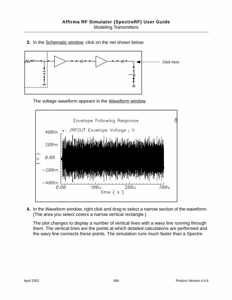
Affirma RF Simulator (SpectreRF) User GuideModeling Transmitters
3. In the Schematic window, click on the net shown below.
The voltage waveform appears in the Waveform window.
4. In the Waveform window, right click and drag to select a narrow section of the waveform.(The area you select covers a narrow vertical rectangle.)
The plot changes to display a number of vertical lines with a wavy line running throughthem. The vertical lines are the points at which detailed calculations are performed andthe wavy line connects these points. The simulation runs much faster than a Spectre
Click here
April 2001 484 Product Version 4.4.6
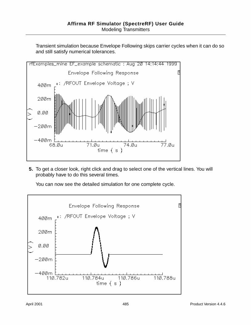
Affirma RF Simulator (SpectreRF) User GuideModeling Transmitters
Transient simulation because Envelope Following skips carrier cycles when it can do soand still satisfy numerical tolerances.
5. To get a closer look, right click and drag to select one of the vertical lines. You willprobably have to do this several times.
You can now see the detailed simulation for one complete cycle.
April 2001 485 Product Version 4.4.6
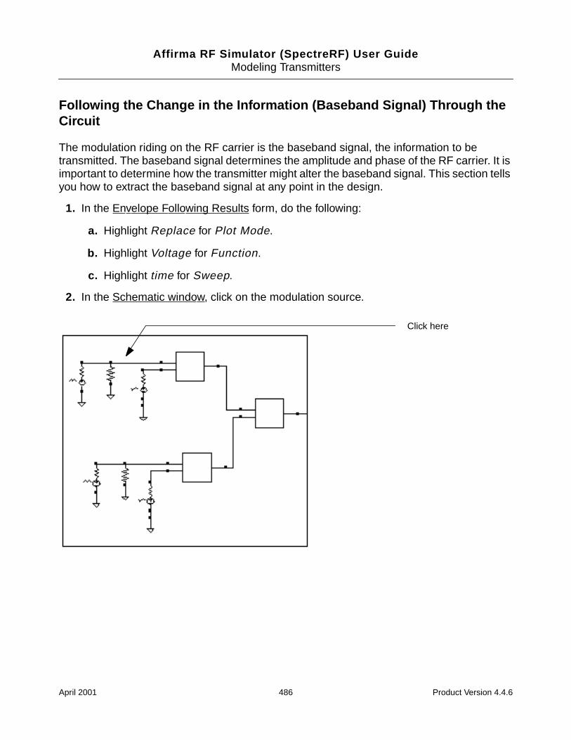
Affirma RF Simulator (SpectreRF) User GuideModeling Transmitters
Following the Change in the Information (Baseband Signal) Through theCircuit
The modulation riding on the RF carrier is the baseband signal, the information to betransmitted. The baseband signal determines the amplitude and phase of the RF carrier. It isimportant to determine how the transmitter might alter the baseband signal. This section tellsyou how to extract the baseband signal at any point in the design.
1. In the Envelope Following Results form, do the following:
a. Highlight Replace for Plot Mode.
b. Highlight Voltage for Function.
c. Highlight time for Sweep.
2. In the Schematic window, click on the modulation source.
Click here
April 2001 486 Product Version 4.4.6
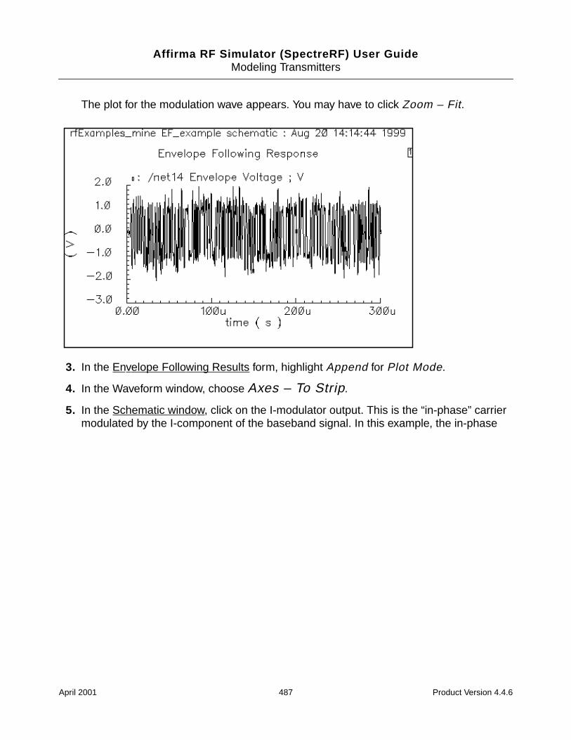
Affirma RF Simulator (SpectreRF) User GuideModeling Transmitters
The plot for the modulation wave appears. You may have to click Zoom – Fit.
3. In the Envelope Following Results form, highlight Append for Plot Mode.
4. In the Waveform window, choose Axes – To Strip.
5. In the Schematic window, click on the I-modulator output. This is the “in-phase” carriermodulated by the I-component of the baseband signal. In this example, the in-phase
April 2001 487 Product Version 4.4.6
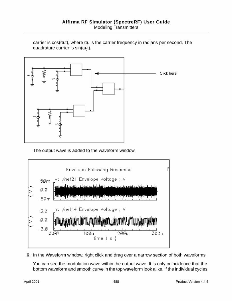
Affirma RF Simulator (SpectreRF) User GuideModeling Transmitters
carrier is cos(ωct), where ωc is the carrier frequency in radians per second. Thequadrature carrier is sin(ωct).
The output wave is added to the waveform window.
6. In the Waveform window, right click and drag over a narrow section of both waveforms.
You can see the modulation wave within the output wave. It is only coincidence that thebottom waveform and smooth curve in the top waveform look alike. If the individual cycles
Click here
April 2001 488 Product Version 4.4.6
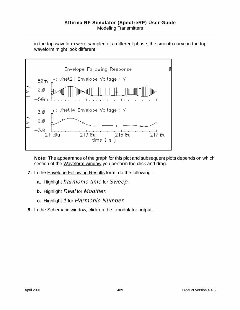
Affirma RF Simulator (SpectreRF) User GuideModeling Transmitters
in the top waveform were sampled at a different phase, the smooth curve in the topwaveform might look different.
Note: The appearance of the graph for this plot and subsequent plots depends on whichsection of the Waveform window you perform the click and drag.
7. In the Envelope Following Results form, do the following:
a. Highlight harmonic time for Sweep.
b. Highlight Real for Modifier.
c. Highlight 1 for Harmonic Number.
8. In the Schematic window, click on the I-modulator output.
April 2001 489 Product Version 4.4.6
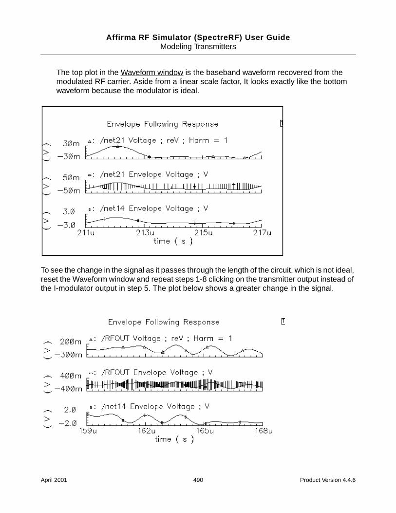
Affirma RF Simulator (SpectreRF) User GuideModeling Transmitters
The top plot in the Waveform window is the baseband waveform recovered from themodulated RF carrier. Aside from a linear scale factor, It looks exactly like the bottomwaveform because the modulator is ideal.
To see the change in the signal as it passes through the length of the circuit, which is not ideal,reset the Waveform window and repeat steps 1-8 clicking on the transmitter output instead ofthe I-modulator output in step 5. The plot below shows a greater change in the signal.
April 2001 490 Product Version 4.4.6

Affirma RF Simulator (SpectreRF) User GuideModeling Transmitters
Plotting the Complete Baseband Signal
1. In the Envelope Following Results form, do the following:
a. Highlight Replace for Plot Mode.
b. Highlight Voltage for Function.
c. Highlight harmonic time for Sweep.
d. Highlight Real for Modifier.
e. Highlight 1 for Harmonic Number.
2. In the Schematic window, click on the adder output.
A plot for the real portion appears in the Waveform window.
3. In the Envelope Following Results form, do the following:
a. Highlight Append for Plot Mode.
b. Highlight Imaginary for Modifier.
4. In the Schematic window, click on the adder output.
A plot for the imaginary portion is added to the Waveform window.
5. In the Waveform window, right click and drag to select a portion of the Waveform windowover a narrow portion of the x-axis.
April 2001 491 Product Version 4.4.6
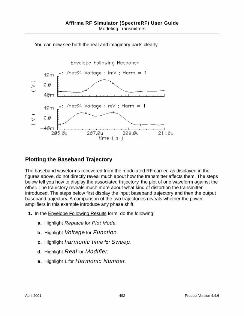
Affirma RF Simulator (SpectreRF) User GuideModeling Transmitters
You can now see both the real and imaginary parts clearly.
Plotting the Baseband Trajectory
The baseband waveforms recovered from the modulated RF carrier, as displayed in thefigures above, do not directly reveal much about how the transmitter affects them. The stepsbelow tell you how to display the associated trajectory, the plot of one waveform against theother. The trajectory reveals much more about what kind of distortion the transmitterintroduced. The steps below first display the input baseband trajectory and then the outputbaseband trajectory. A comparison of the two trajectories reveals whether the poweramplifiers in this example introduce any phase shift.
1. In the Envelope Following Results form, do the following:
a. Highlight Replace for Plot Mode.
b. Highlight Voltage for Function.
c. Highlight harmonic time for Sweep.
d. Highlight Real for Modifier.
e. Highlight 1 for Harmonic Number.
April 2001 492 Product Version 4.4.6
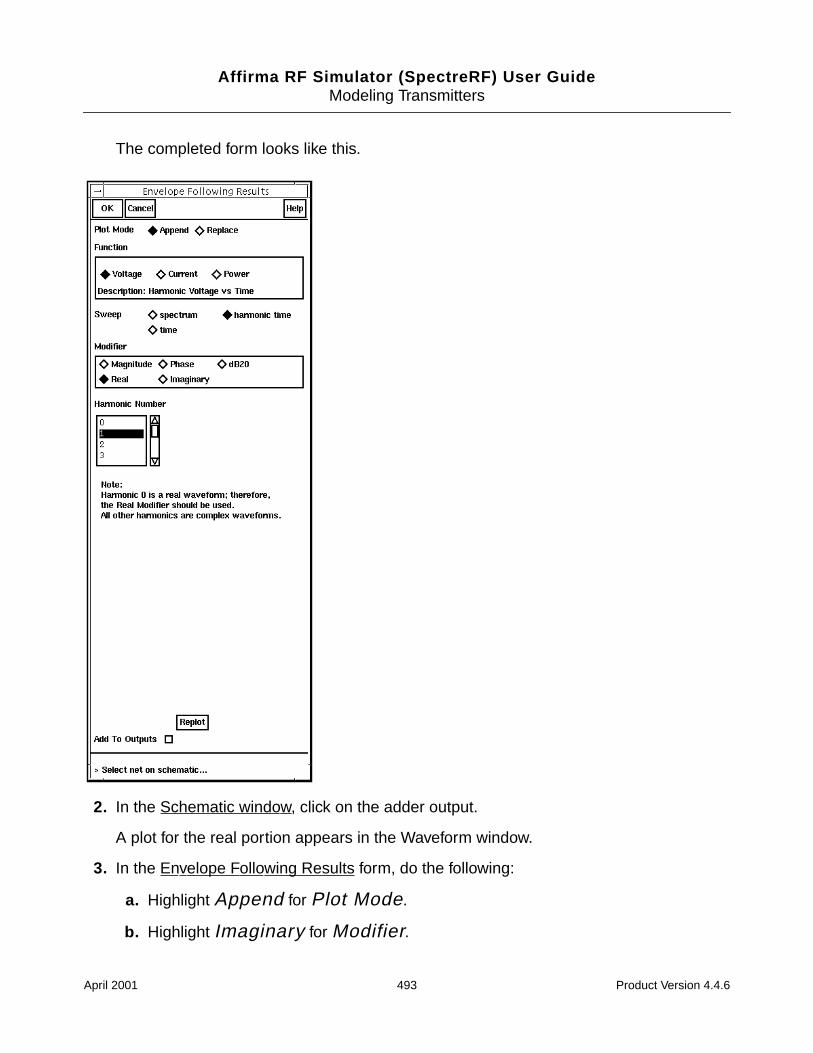
Affirma RF Simulator (SpectreRF) User GuideModeling Transmitters
The completed form looks like this.
2. In the Schematic window, click on the adder output.
A plot for the real portion appears in the Waveform window.
3. In the Envelope Following Results form, do the following:
a. Highlight Append for Plot Mode.
b. Highlight Imaginary for Modifier.
April 2001 493 Product Version 4.4.6
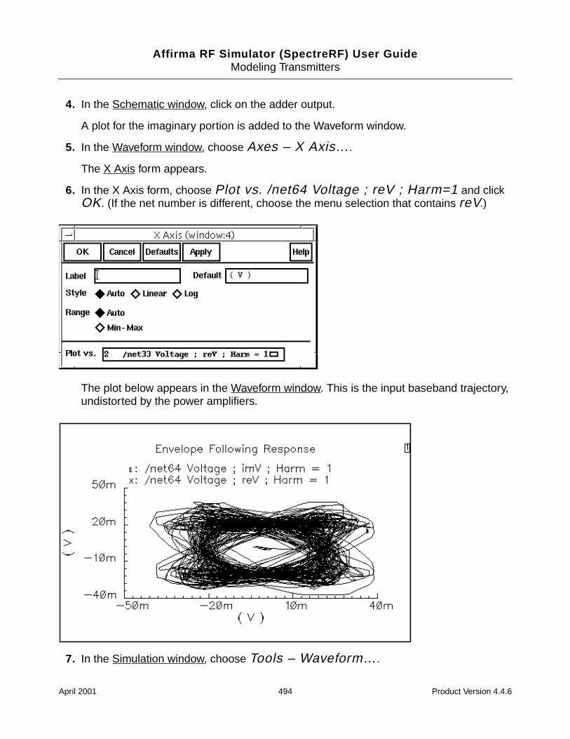
Affirma RF Simulator (SpectreRF) User GuideModeling Transmitters
4. In the Schematic window, click on the adder output.
A plot for the imaginary portion is added to the Waveform window.
5. In the Waveform window, choose Axes – X Axis….
The X Axis form appears.
6. In the X Axis form, choose Plot vs. /net64 Voltage ; reV ; Harm=1 and clickOK. (If the net number is different, choose the menu selection that contains reV.)
The plot below appears in the Waveform window. This is the input baseband trajectory,undistorted by the power amplifiers.
7. In the Simulation window, choose Tools – Waveform….
April 2001 494 Product Version 4.4.6
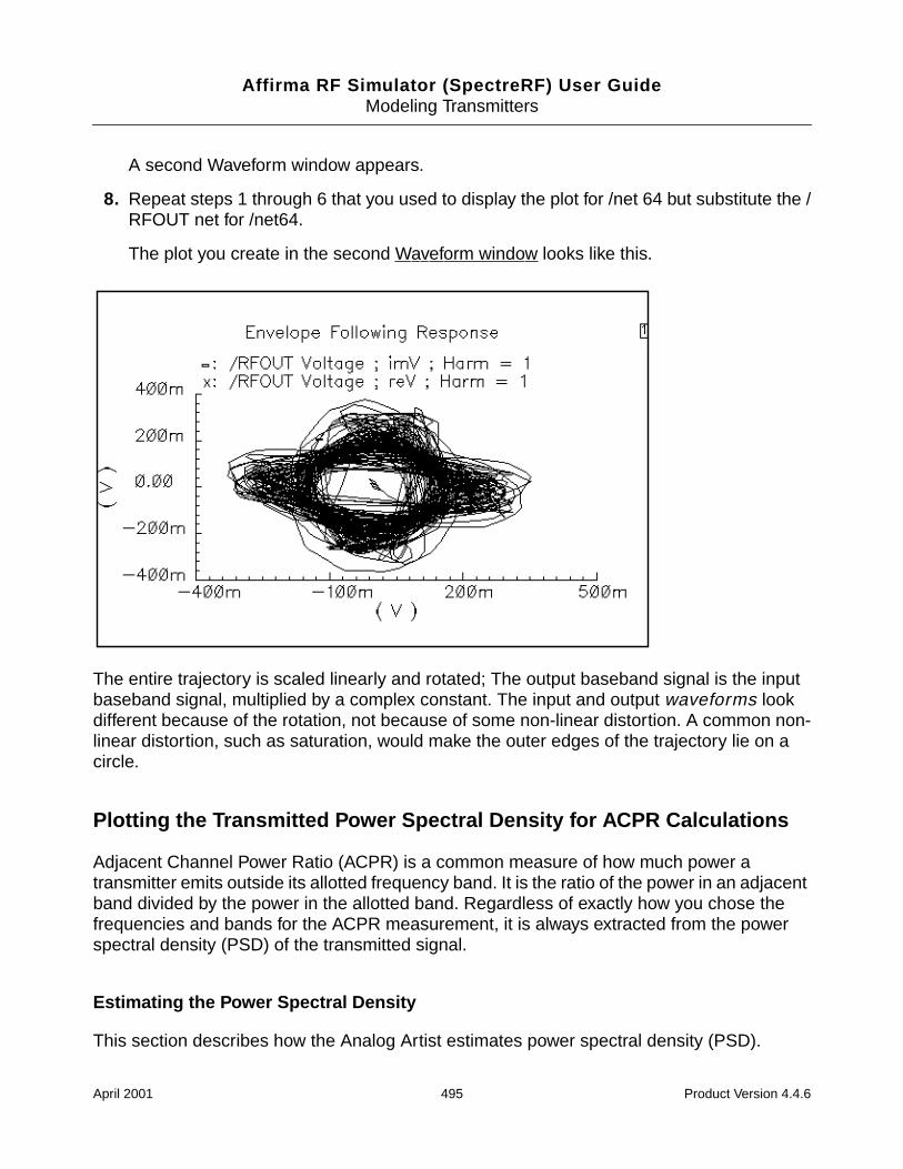
Affirma RF Simulator (SpectreRF) User GuideModeling Transmitters
A second Waveform window appears.
8. Repeat steps 1 through 6 that you used to display the plot for /net 64 but substitute the /RFOUT net for /net64.
The plot you create in the second Waveform window looks like this.
The entire trajectory is scaled linearly and rotated; The output baseband signal is the inputbaseband signal, multiplied by a complex constant. The input and output waveforms lookdifferent because of the rotation, not because of some non-linear distortion. A common non-linear distortion, such as saturation, would make the outer edges of the trajectory lie on acircle.
Plotting the Transmitted Power Spectral Density for ACPR Calculations
Adjacent Channel Power Ratio (ACPR) is a common measure of how much power atransmitter emits outside its allotted frequency band. It is the ratio of the power in an adjacentband divided by the power in the allotted band. Regardless of exactly how you chose thefrequencies and bands for the ACPR measurement, it is always extracted from the powerspectral density (PSD) of the transmitted signal.
Estimating the Power Spectral Density
This section describes how the Analog Artist estimates power spectral density (PSD).
April 2001 495 Product Version 4.4.6
Affirma RF Simulator (SpectreRF) User GuideModeling Transmitters
PSDs are always estimated because the information riding on the carrier is a stochasticprocess and the Fourier transform of a stochastic process is ill defined. No matter how youchose to define the spectral nature of a stochastic process, it always involves an averagingprocess. Any empirically derived average is an estimate because you can never take aninfinite number of samples.
The PSD is a frequency-by-frequency average of a set of DFTs (discrete Fourier transforms)of the baseband signal. Here, the baseband signal is the harmonic-time results of anEnvelope Following analysis. The parameters that control the PSD estimate described below.
The Time Interval specifies the time record you wish to analyze in the frequency domain.The time interval should be long enough to support the frequency resolution you want.
The Nyquist half bandwidth is half the sampling frequency used in the DFTs. Make thisbig enough to prevent aliasing; the true spectrum of the baseband signal should benegligible at this frequency and beyond.
The Frequency bin width is the frequency resolution you want. If you chose a small binwidth, the resulting PSD will look “noisy”. The PSD will have a jagged appearance. If youmake the bin width too large you may soften what should be sharp edges in thespectrum.
The waveform is first interpolated, if necessary, to generate evenly spaced data points in time.The spacing of the data points is the inverse of the DFT sampling frequency. The PSD iscomputed by first breaking the time interval up into overlapping segments. Each segment ismultiplied, time point by time point, by the specified Windowing function. Windowing reduceserrors caused by a finite time record. It is impossible to work with an infinite time record. Directuse of an unwindowed finite time record is equivalent to multiplying the infinite record by arectangular pulse that lasts as long as the data record. Multiplication in the time domaincorresponds to convolution in the frequency domain. The Fourier transform of a rectangularpulse is a sinc function. Considering the frequency domain convolution, the side lobes of thesinc function cause parts of the true spectrum to “leak” into the frequency of interest, thefrequency of the main lobe. Ideally, the sinc function would be a Dirac delta function but thatrequires an infinite time record. Good window functions have smaller side lobes than a sincfunction.
The DFT is performed on each windowed segment of the baseband waveform. At eachfrequency, the DFTs from all segments are averaged together. Fewer segments means fewerdata points in the average at a particular frequency. The length of each segment is inverselyproportional to the frequency bin width. That is why a small bin width produces a jagged PSD.A smaller bin width means a longer time segment. Fewer long segments fit into the given timeinterval so there are fewer DFTs to average together. In the extreme, there is only onesegment and no averaging. Without averaging, the PSD is just the square of the magnitudeof the DFT of a stochastic process. At the other extreme, large bin widths produce lots ofpoints to average at each frequency but there are fewer frequencies at which to average.
April 2001 496 Product Version 4.4.6
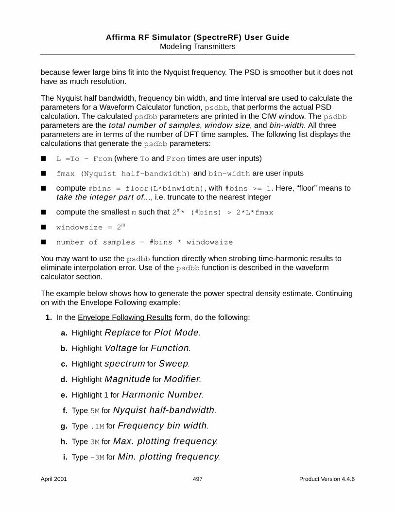
Affirma RF Simulator (SpectreRF) User GuideModeling Transmitters
because fewer large bins fit into the Nyquist frequency. The PSD is smoother but it does nothave as much resolution.
The Nyquist half bandwidth, frequency bin width, and time interval are used to calculate theparameters for a Waveform Calculator function, psdbb , that performs the actual PSDcalculation. The calculated psdbb parameters are printed in the CIW window. The psdbbparameters are the total number of samples, window size, and bin-width. All threeparameters are in terms of the number of DFT time samples. The following list displays thecalculations that generate the psdbb parameters:
L =To - From (where To and From times are user inputs)
fmax (Nyquist half-bandwidth) and bin-width are user inputs
compute #bins = floor(L*binwidth) , with #bins >= 1 . Here, “floor” means totake the integer part of..., i.e. truncate to the nearest integer
compute the smallest m such that 2m* (#bins) > 2*L*fmax
windowsize = 2 m
number of samples = #bins * windowsize
You may want to use the psdbb function directly when strobing time-harmonic results toeliminate interpolation error. Use of the psdbb function is described in the waveformcalculator section.
The example below shows how to generate the power spectral density estimate. Continuingon with the Envelope Following example:
1. In the Envelope Following Results form, do the following:
a. Highlight Replace for Plot Mode.
b. Highlight Voltage for Function.
c. Highlight spectrum for Sweep.
d. Highlight Magnitude for Modifier.
e. Highlight 1 for Harmonic Number.
f. Type 5M for Nyquist half-bandwidth.
g. Type .1M for Frequency bin width.
h. Type 3M for Max. plotting frequency.
i. Type -3M for Min. plotting frequency.
April 2001 497 Product Version 4.4.6
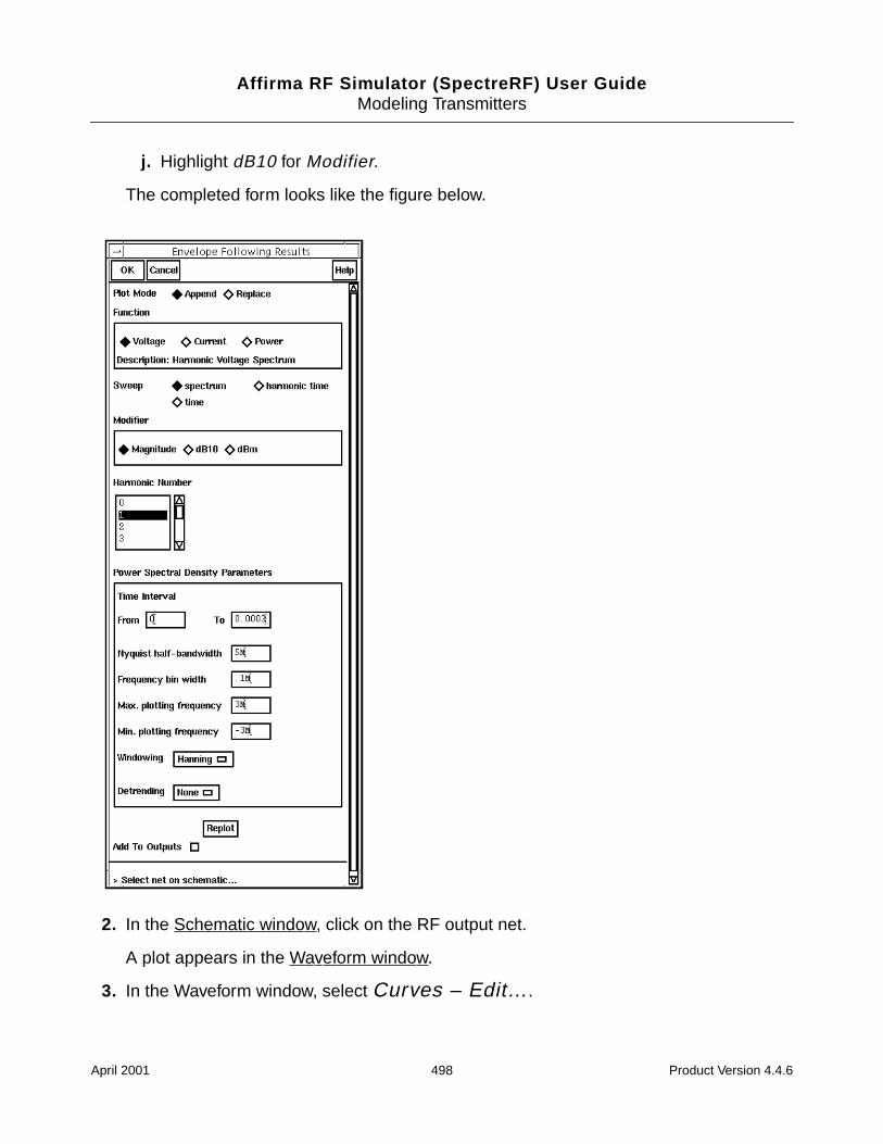
Affirma RF Simulator (SpectreRF) User GuideModeling Transmitters
j. Highlight dB10 for Modifier.
The completed form looks like the figure below.
2. In the Schematic window, click on the RF output net.
A plot appears in the Waveform window.
3. In the Waveform window, select Curves – Edit….
April 2001 498 Product Version 4.4.6
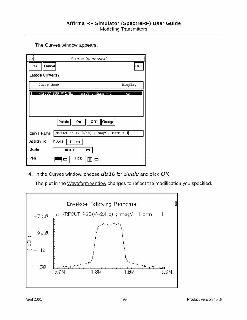
Affirma RF Simulator (SpectreRF) User GuideModeling Transmitters
The Curves window appears.
4. In the Curves window, choose dB10 for Scale and click OK.
The plot in the Waveform window changes to reflect the modification you specified.
April 2001 499 Product Version 4.4.6
Affirma RF Simulator (SpectreRF) User GuideModeling Transmitters
You can now calculate the ACPR for two x-axis values by subtracting their associated y-axis values. (The ACPR measured with respect to x1 and x2 is y1 - y2.)
For example, given the following spectral parameters, the adjacent channel is 2.5 MHzfrom the carrier and you choose to define ACPR in terms of power at just twofrequencies, you can use the cursor to determine the RF output power at 2.5 MHz andzero frequency.
The power at 2.5 MHz equals -119.7 dB and the power near zero (at 18.56 KHz) equals-77.48 dB. (Remember that the horizontal scale is frequency offset from the carrierfundamental.) The difference between these measurements equals -42.22 dB. For thisdefinition of ACPR, ACPR = -42.22 dB.
Other definitions of ACPR are possible. You can compute them by adjusting the spectralparameters and applying the waveform calculator to the spectral plot.
Calculation of Power Spectral Density
Power spectral density results are calculated in the following manner. For a constantbaseband signal, and
Baseband signal = i + j*q, where j = sqrt(-1)
Passband signal = i*cos(w*t)-q*sin(w*t)
The power of the baseband signal is
Baseband signal power = i*i + q*q volts*volts
The power of the passband signal is
Passband signal power = i*i/2 + q*q/2 = (1/2)*( baseband power )
Envelope Spectral analysis computes these values per Hz. They can also be expressedas
(rms passband volts)*(rms passband volts)/Hz
The Envelope Time-Harmonic analysis computes peak volts because they can bedirectly compared with the modulating signals.
For the example, you see a waveform displayed in versus frequency. You canthink of this as (rms passband volts)*(rms passband volts)/Hz . Thedisplayed spectrum is the estimated power spectral density of the complex envelope,divided by two. The division by two is there because the envelope is in units of peakcarrier volts but power in the carrier equals the square of the peak, divided by two. It isconvenient to express the envelope in peak units because it can then be directlycompared against an input baseband signal.
V2
Hz( )⁄
April 2001 500 Product Version 4.4.6
Affirma RF Simulator (SpectreRF) User GuideModeling Transmitters
PSD and the Baseband Signal to be Transmitted
The baseband signal driving the transmitter dominates the transmitted PSD. In most cases,the baseband signals come from digital filters. The digital filters constrain the spectrum of theinput baseband signal. Distortion in the transmitter causes the spectrum to grow where itshould not, hence the need for an ACPR measurement. In measuring ACPR it is crucial todrive the transmitter with the proper baseband signals.
It is not practical to model digital filters in SpectreRF because SpectreRF cannot simulatestate variables inside Verilog-A modules. Consequently, for now, you must pre-compute andstore the baseband inputs. You then read them into the SpectreRF analysis through the ppwlfsources found in the analogLib, as shown in this example. The ppwlf sources also read SPWformat, so you can also generate and record the input baseband waveforms using SPW.
The rfLib contains three sets of stored baseband waveforms, cdma, dqpsk, and gsm. Thesewaveforms were created with the baseband signal generators in the measurement categoryof the rfLib.
If you want to measure ACPR with the noise floor much more than 40dB below the peak ofthe output power spectral density, you will have to create baseband drive signals with a noisefloor at or below the required noise floor. If you use a DSP tool such as SPW to create thesignals, the filters in the baseband signal generator will have to operate perhaps hundreds oftimes faster than those in the actual generator.
Note: Sometimes an ACPR specification exceeds the ACPR of the baseband drive signals.To see if the transmitter meets specifications in that event, it must be driven with an unrealisticbaseband signal.
Otherwise the signals will not have enough resolution. The noise floor depends heavily oninterpolation error.
Note: The Fourier analysis used to compute the power spectral density uses evenly spacedtime points. If data does not exist at one of the Fourier time points, the Fourier algorithm mustinterpolate to create one.
You can strobe the harmonic time results to eliminate interpolation of the output but youcannot eliminate interpolation of the baseband drive signals. The only way to reduceinterpolation errors at the input is to use ultra-high-resolution drive signals so that no matterwhere the interpolation occurs, the error is small. For now, it is up to you to generate ultra-high-resolution drive signals.
The following results were obtained by generating high resolution baseband signals in SPW,storing them, then reading them into the Envelope Following simulation through the pwlsources. The FIR filters inside SPW operated at 300 times the chip rate.
April 2001 501 Product Version 4.4.6
Affirma RF Simulator (SpectreRF) User GuideModeling Transmitters
Figure 11-1 on page 502 shows the spectrum at the output of the adder, which is where theRF signal is undistorted in this model, computed with three different “number of samples”.The simulation was run with reltol set to 1e-5 and the Envelope Following analysis optioncalled “strobeperiod” set to 100ns. If strobeperiod does not equal an integer number ofclock cycles, it is internally truncated to an integer number of clock cycles. The timeinterval for the psdbb function was from 100us to 1ms. The window size 1 was 1024 samplesand the window function was “Hanning”.With strobeperiod set to 100ns (100 clock cycles),the simulation produced 9000 evenly spaced samples inside the time interval. The spectrawere calculated for 8500, 8750, 9000, 9250, and 9500 points for the “number of samples”.The figure clearly shows interpolation errors when the number of samples used in the psdbbfunction does not equal the actual number of samples.
Figure 11-1 Spectrum at the Output Adder Computed with Three Different Number ofSamples
The figure below compares the input and output PSDs using the high resolution drive signalsand the following set of psdbb parameters:
From=100u
To=1m
1. “Window size” must be a power of 2. If you enter something that is not a power of 2, the psdbb function willtruncate to the nearest power of 2.
April 2001 502 Product Version 4.4.6
Affirma RF Simulator (SpectreRF) User GuideModeling Transmitters
Number of Samples=9000
Window size=1024
Window Type=Hanning
The top PSD is from the power amplifier output and clearly shows spectral regrowth whencompared to the input PSD.
April 2001 503 Product Version 4.4.6
Affirma RF Simulator (SpectreRF) User GuideModeling Transmitters
Measuring Load Pull Contours and ReflectionCoefficients
A load pull contour is a set of points on a Smith chart representing all the loads that dissipatea given amount of power. Just as a topographical map shows a hiker where the mountainpeak lies and how steep the climb is, load pull contours show which load dissipates the mostpower and how sensitive that power is to small load perturbations. Load pull contours helpyou match a load to a power amplifier for maximum power transfer. This section describeshow to generate load pull contours and determine whether the input matching network mustbe redesigned for the optimal load.
To properly use Load-Pull results, you must understand how the Load-Pull feature definesreflection coefficients. Reflection coefficients are computed from the SpectreRF PSSanalysis.The load reflection coefficient is computed from the load impedance, which iscomputed as the ratio of the voltage across the load to the current flowing into the load at theRF carrier frequency. Suppose the RF carrier is 1GHz and the load waveforms are distorted.The impedance is not computed from small-signal perturbations about an operating point.Rather, it is computed as the ratio of the 1GHz components of the load voltage and currentwaveforms simulated by a PSS run. Because the load is passive and linear, the load reflectioncoefficient computed in this manner equals the small-signal, or incrementally computed, loadimpedance.
This is not necessarily true for the input reflection coefficient because the input circuitry canbe non-linear and also contain input offset voltages and currents. However, becausematching networks are usually designed only for the RF fundamental, defining the reflectioncoefficient as the ratio of fundamental Fourier components of the large signals is oftenjustified.
Setting Up and Running the Simulation
This example tells you how to modify the EF_example schematic and then how to measureLoad Pull Contours and Reflection Coefficients for the modified design.
Before you start, perform the setup procedures described in Chapter 3.
Opening the EF_examples Schematic
1. In the CIW, choose File – Open….
April 2001 504 Product Version 4.4.6

Affirma RF Simulator (SpectreRF) User GuideModeling Transmitters
The Open File form appears.
2. In the Open File form, do the following:
a. Choose rfExamples for Library Name.
Select the editable copy of the rfExamples library you created following theinstructions in Chapter 3.
b. In the Cell Name list box, highlight EF_example.
c. Choose schematic for View Name.
d. Highlight edit for Mode.
e. Click OK.
April 2001 505 Product Version 4.4.6
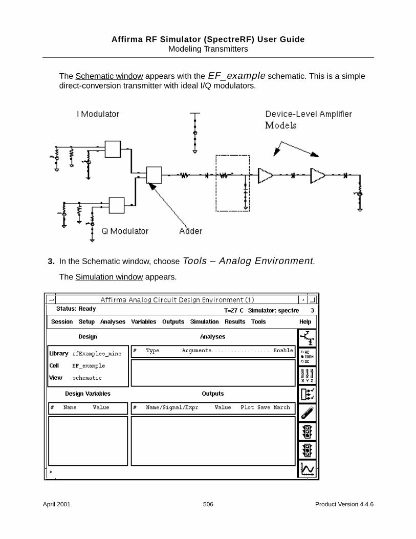
Affirma RF Simulator (SpectreRF) User GuideModeling Transmitters
The Schematic window appears with the EF_example schematic. This is a simpledirect-conversion transmitter with ideal I/Q modulators.
3. In the Schematic window, choose Tools – Analog Environment.
The Simulation window appears.
April 2001 506 Product Version 4.4.6
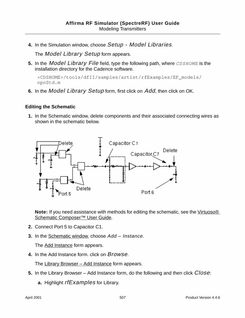
Affirma RF Simulator (SpectreRF) User GuideModeling Transmitters
4. In the Simulation window, choose Setup - Model Libraries.
The Model Library Setup form appears.
5. In the Model Library File field, type the following path, where CDSHOME is theinstallation directory for the Cadence software.
<CDSHOME>/tools/dfII/samples/artist/rfExamples/EF_models/npnStd.m
6. In the Model Library Setup form, first click on Add, then click on OK.
Editing the Schematic
1. In the Schematic window, delete components and their associated connecting wires asshown in the schematic below.
Note: If you need assistance with methods for editing the schematic, see the Virtuoso®Schematic Composer™ User Guide.
2. Connect Port 5 to Capacitor C1.
3. In the Schematic window, choose Add – Instance.
The Add Instance form appears.
4. In the Add Instance form. click on Browse.
The Library Browser – Add Instance form appears.
5. In the Library Browser – Add Instance form, do the following and then click Close:
a. Highlight rfExamples for Library.
April 2001 507 Product Version 4.4.6
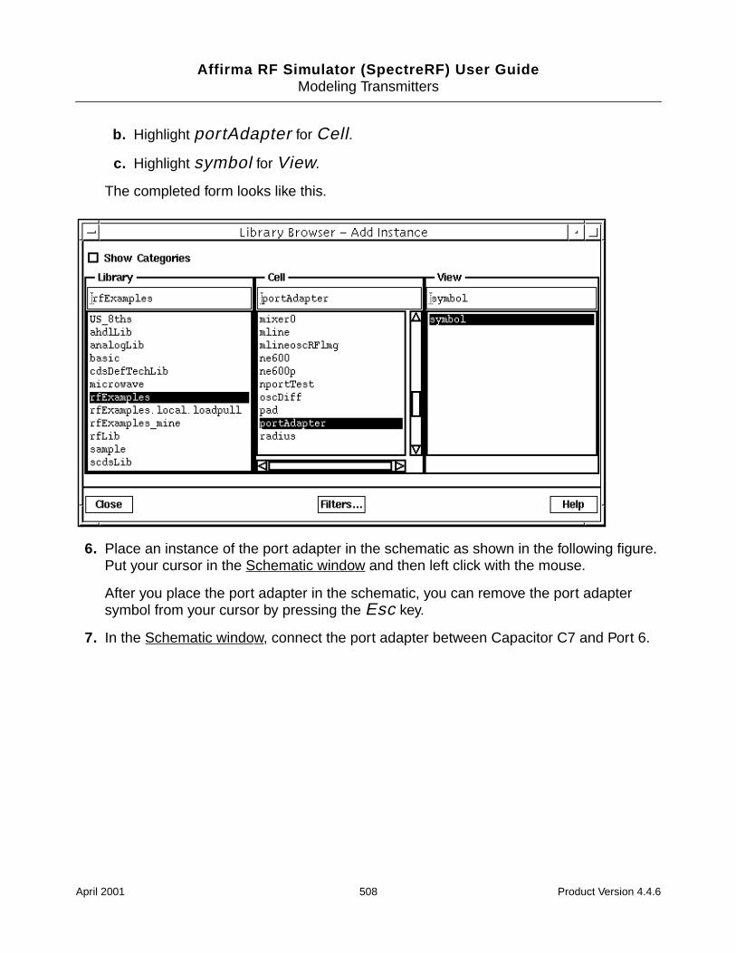
Affirma RF Simulator (SpectreRF) User GuideModeling Transmitters
b. Highlight portAdapter for Cell.
c. Highlight symbol for View.
The completed form looks like this.
6. Place an instance of the port adapter in the schematic as shown in the following figure.Put your cursor in the Schematic window and then left click with the mouse.
After you place the port adapter in the schematic, you can remove the port adaptersymbol from your cursor by pressing the Esc key.
7. In the Schematic window, connect the port adapter between Capacitor C7 and Port 6.
April 2001 508 Product Version 4.4.6
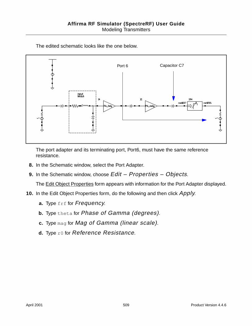
Affirma RF Simulator (SpectreRF) User GuideModeling Transmitters
The edited schematic looks like the one below.
The port adapter and its terminating port, Port6, must have the same referenceresistance.
8. In the Schematic window, select the Port Adapter.
9. In the Schematic window, choose Edit – Properties – Objects.
The Edit Object Properties form appears with information for the Port Adapter displayed.
10. In the Edit Object Properties form, do the following and then click Apply.
a. Type frf for Frequency.
b. Type theta for Phase of Gamma (degrees).
c. Type mag for Mag of Gamma (linear scale).
d. Type r0 for Reference Resistance.
Port 6 Capacitor C7
April 2001 509 Product Version 4.4.6
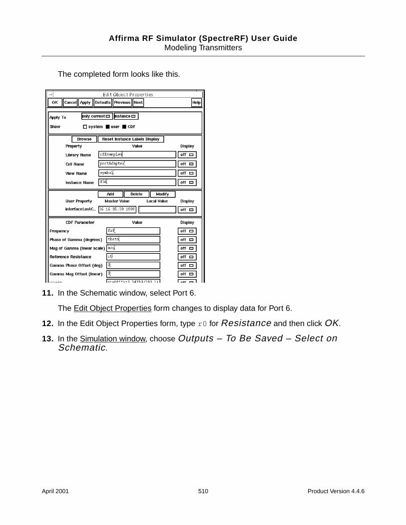
Affirma RF Simulator (SpectreRF) User GuideModeling Transmitters
The completed form looks like this.
11. In the Schematic window, select Port 6.
The Edit Object Properties form changes to display data for Port 6.
12. In the Edit Object Properties form, type r0 for Resistance and then click OK.
13. In the Simulation window, choose Outputs – To Be Saved – Select onSchematic.
April 2001 510 Product Version 4.4.6
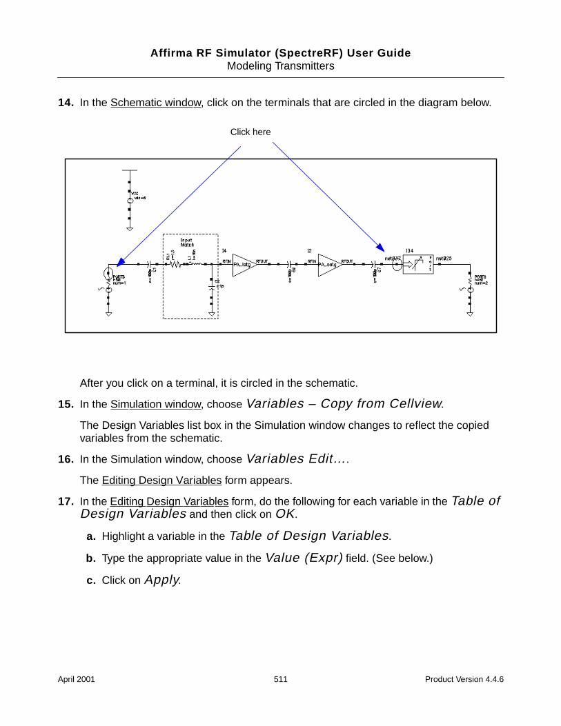
Affirma RF Simulator (SpectreRF) User GuideModeling Transmitters
14. In the Schematic window, click on the terminals that are circled in the diagram below.
After you click on a terminal, it is circled in the schematic.
15. In the Simulation window, choose Variables – Copy from Cellview.
The Design Variables list box in the Simulation window changes to reflect the copiedvariables from the schematic.
16. In the Simulation window, choose Variables Edit….
The Editing Design Variables form appears.
17. In the Editing Design Variables form, do the following for each variable in the Table ofDesign Variables and then click on OK.
a. Highlight a variable in the Table of Design Variables.
b. Type the appropriate value in the Value (Expr) field. (See below.)
c. Click on Apply.
Click here
April 2001 511 Product Version 4.4.6

Affirma RF Simulator (SpectreRF) User GuideModeling Transmitters
The table shows you the appropriate value for each variable.
18. In the Simulation window, choose Design – Check and Save.
Performing the Simulation
1. In the Simulation window, choose Analyses – Choose….
The Choosing Analyses form appears.
2. In the Choosing Analyses form, highlight PSS.
The form changes to display options for PSS simulation.
3. In the Choosing Analyses form, do the following and then click OK:
a. If information for frf is not displayed in the Fundamental Tones list box, type frfin the Name field below the list box and click Clear/Add.
b. Click Update From Schematic to update the values in the Fundamental Toneslist box from the schematic. Note that before you can update from the schematic, youmust perform a Check and Save on the design.
c. Highlight the Auto Calculate button to automatically calculate and enter a valuein the Beat Frequency field.
d. Choose Number of Harmonics for Output harmonics and type 9 in theadjacent field.
e. Highlight the Sweep button and choose Variable in the associated cyclic field.
f. Type theta for Variable Name (or click on Select Design Variable andhighlight theta in the form that appears).
g. Choose Start – Stop for Sweep Range.
h. Type 0 for the Start value and 359 for the Stop value.
Variable Value
theta 0
r0 50
mag 0
frf 1G
April 2001 512 Product Version 4.4.6
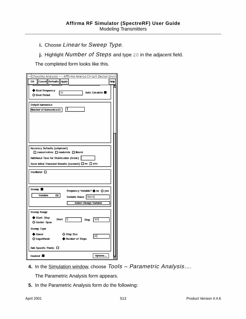
Affirma RF Simulator (SpectreRF) User GuideModeling Transmitters
i. Choose Linear for Sweep Type.
j. Highlight Number of Steps and type 20 in the adjacent field.
The completed form looks like this.
4. In the Simulation window, choose Tools – Parametric Analysis….
The Parametric Analysis form appears.
5. In the Parametric Analysis form do the following:
April 2001 513 Product Version 4.4.6
Affirma RF Simulator (SpectreRF) User GuideModeling Transmitters
a. Type mag for Variable Name.
b. Choose From/To for Range Type and type 0 for From and .95 for To in theadjacent fields.
c. Choose Linear for Step Control and type 10 in the adjacent Total Stepsfield.
d. Choose Analysis – Start.
Look in the CIW for a message that says the simulation completes successfully.
Displaying Load Contours
1. In the Simulation window, choose Results – Direct Plot – PSS….
The PSS Results form appears.
2. In the PSS Results form, do the following:
a. Highlight Replace for Plot Mode.
b. Highlight Power Contours for Function.
c. Highlight Magnitude for Power Modifier.
d. Type 9 for Number of Contours, if necessary.
e. Type 50.0 for Reference Resistance, if necessary.
f. Highlight 1 1G for Output Harmonic.
You select a different harmonic if the PSS fundamental frequency is smaller than 1GHz. Forexample, if another part of the circuit is driven at 1.5 GHz, the fundamental will be 500MHz.But because the part of the circuit where you want to do load-pull analysis operates at 1GHz,in order to plot the correct contours, the contours associated with 1GHz, you must specify thesecond harmonic of the fundamental, 2*500MHz = 1GHz.
April 2001 514 Product Version 4.4.6
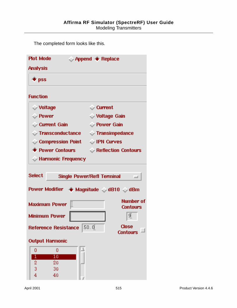
Affirma RF Simulator (SpectreRF) User GuideModeling Transmitters
The completed form looks like this.
April 2001 515 Product Version 4.4.6
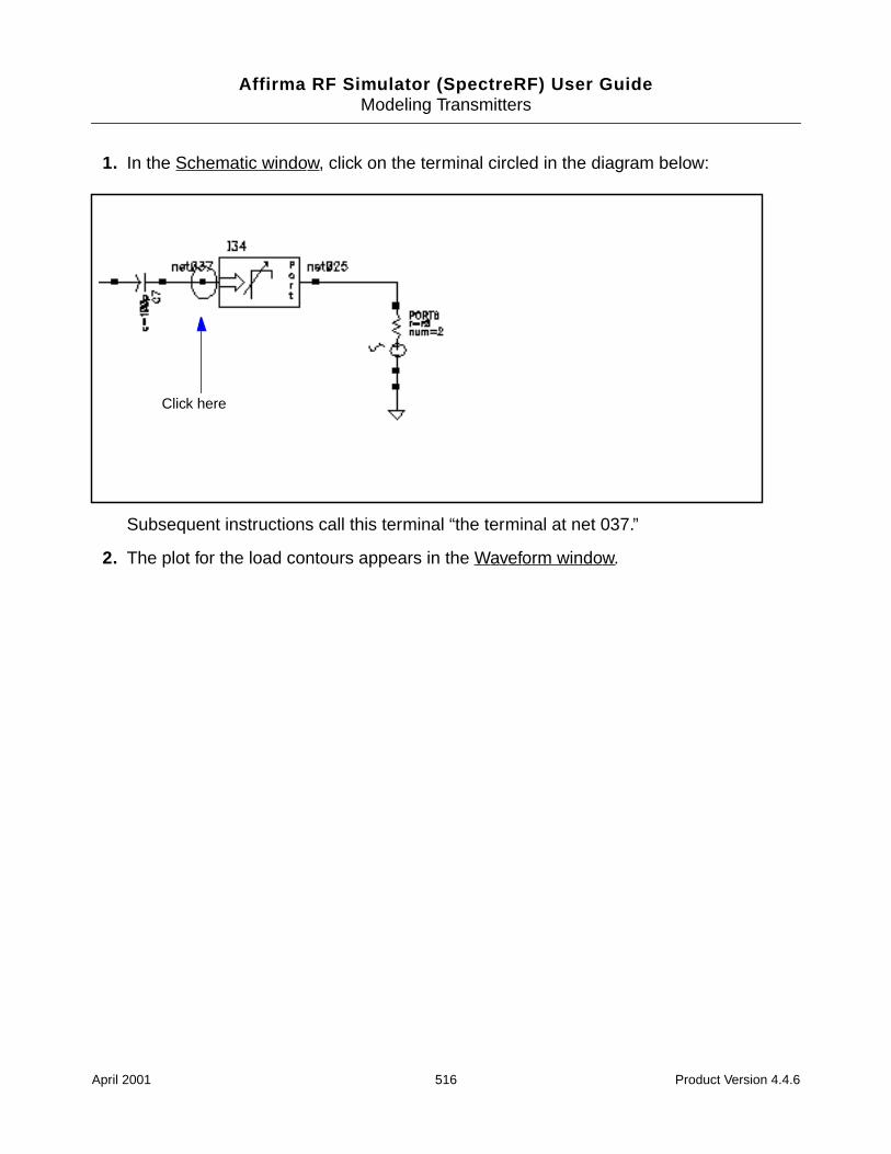
Affirma RF Simulator (SpectreRF) User GuideModeling Transmitters
1. In the Schematic window, click on the terminal circled in the diagram below:
Subsequent instructions call this terminal “the terminal at net 037.”
2. The plot for the load contours appears in the Waveform window.
Click here
April 2001 516 Product Version 4.4.6
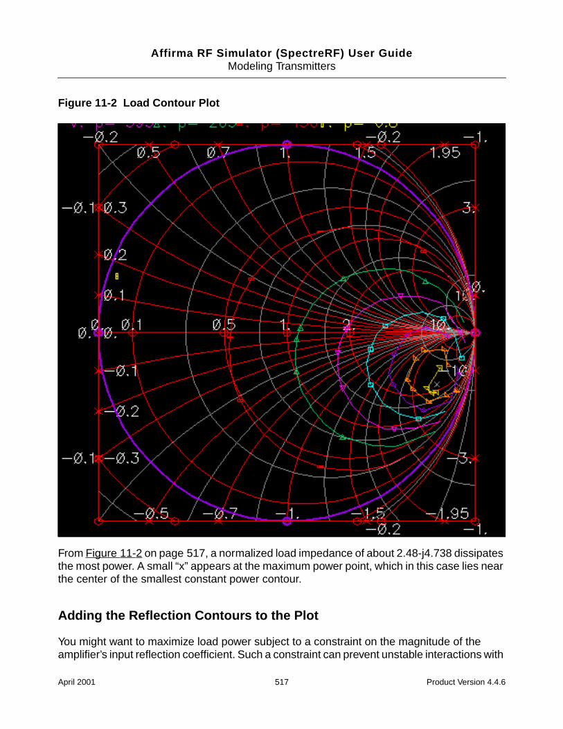
Affirma RF Simulator (SpectreRF) User GuideModeling Transmitters
Figure 11-2 Load Contour Plot
From Figure 11-2 on page 517, a normalized load impedance of about 2.48-j4.738 dissipatesthe most power. A small “x” appears at the maximum power point, which in this case lies nearthe center of the smallest constant power contour.
Adding the Reflection Contours to the Plot
You might want to maximize load power subject to a constraint on the magnitude of theamplifier’s input reflection coefficient. Such a constraint can prevent unstable interactions with
April 2001 517 Product Version 4.4.6

Affirma RF Simulator (SpectreRF) User GuideModeling Transmitters
the preceding stage. You can overlay load-pull contours with contours of constant inputreflection coefficient magnitude. The optimal load corresponds to the reflection coefficientthat lies on the “largest power” load-pull contour and also lies on a constant input reflectioncoefficient contour that is within the constraint. Here, “largest power” means the contourcorresponding to the largest amount of power delivered to the load. To use the topographicalmap analogy again, this is like overlaying constant elevation contours and contours ofconstant temperature. The optimization objective would be like trying to find the highest pointon the mountain such that the temperature is greater than 60 degrees.
1. In the PSS Results form, do the following:
a. Highlight Append for Plot Mode.
b. Highlight Reflection Contours for Function.
c. Select Separate Refl and RefRefl Terminals.
d. Type 9 for Number of Contours, if necessary.
e. Type 50.0 for Reference Resistance, if necessary.
f. Highlight 1 1G for Output Harmonic.
April 2001 518 Product Version 4.4.6
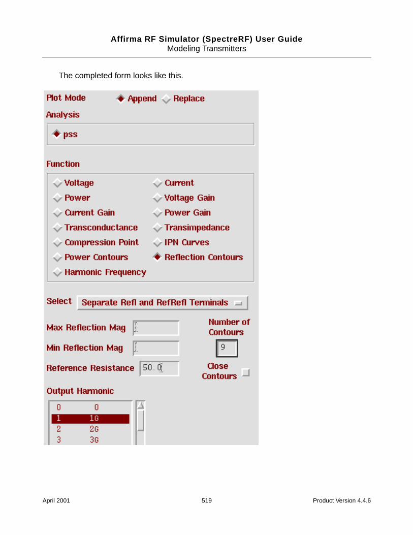
Affirma RF Simulator (SpectreRF) User GuideModeling Transmitters
The completed form looks like this.
April 2001 519 Product Version 4.4.6
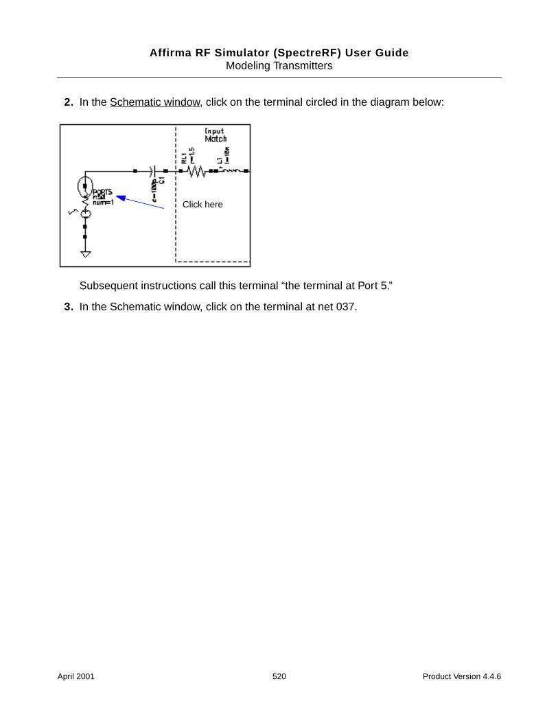
Affirma RF Simulator (SpectreRF) User GuideModeling Transmitters
2. In the Schematic window, click on the terminal circled in the diagram below:
Subsequent instructions call this terminal “the terminal at Port 5.”
3. In the Schematic window, click on the terminal at net 037.
Click here
April 2001 520 Product Version 4.4.6
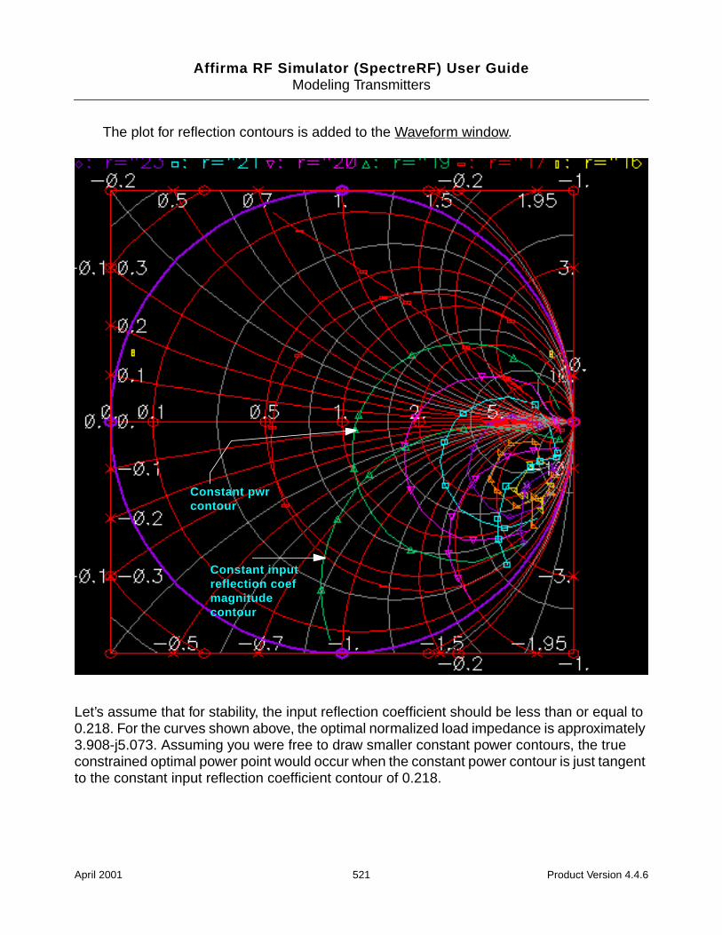
Affirma RF Simulator (SpectreRF) User GuideModeling Transmitters
The plot for reflection contours is added to the Waveform window.
Let’s assume that for stability, the input reflection coefficient should be less than or equal to0.218. For the curves shown above, the optimal normalized load impedance is approximately3.908-j5.073. Assuming you were free to draw smaller constant power contours, the trueconstrained optimal power point would occur when the constant power contour is just tangentto the constant input reflection coefficient contour of 0.218.
Constant pwrcontour
Constant inputreflection coefmagnitudecontour
April 2001 521 Product Version 4.4.6

Affirma RF Simulator (SpectreRF) User GuideModeling Transmitters
Are Constant Power Contours the Same as Constant Gain Contours?
In general, constant power contours are not the same as constant power gain contours. Thesimulator does not maintain any input impedance match while it sweeps the load to generateload-pull contours. The resulting contours are not constant power gain contours, but are onlyconstant power contours. However, if the input reflection coefficient and input power do notchange much over the load sweep range, the generated contours are good approximationsof constant gain contours. By plotting constant power contours in the input reflectioncoefficient plane, you can see how both changed during the sweep of load reflectioncoefficient. If the input power does not vary with load, the constant power contours are alsoconstant power gain contours. If it does vary, the contours tell you how much you have tochange the input matching network during the load sweep to maintain a constant input power.
1. In the PSS Results form, do the following:
a. Highlight Replace for Plot Mode.
b. Highlight Power Contours for Function.
c. Highlight Select Power/Ref Terminal.
d. Type 9 for Number of Contours, if necessary.
e. Type 50.0 for Reference Resistance, if necessary.
f. Highlight 1G for Output Harmonic.
April 2001 522 Product Version 4.4.6
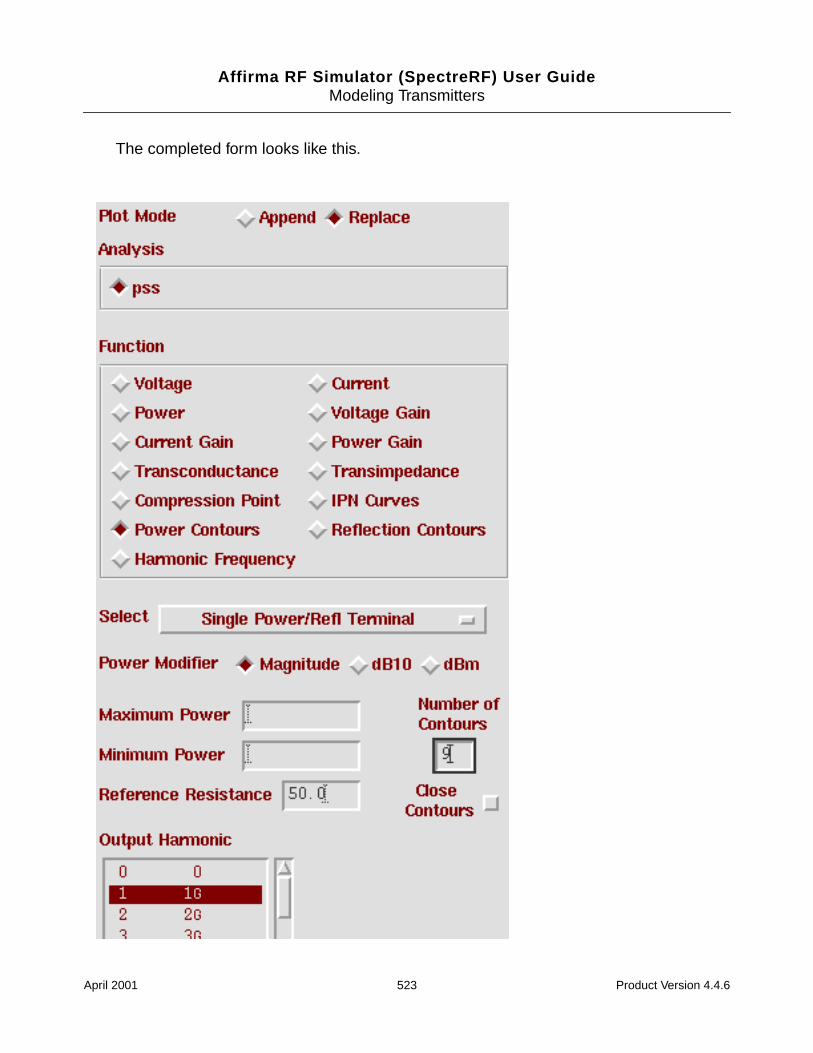
Affirma RF Simulator (SpectreRF) User GuideModeling Transmitters
The completed form looks like this.
April 2001 523 Product Version 4.4.6
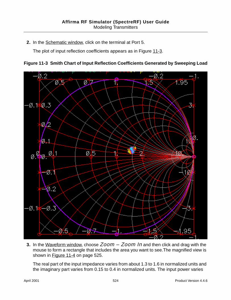
Affirma RF Simulator (SpectreRF) User GuideModeling Transmitters
2. In the Schematic window, click on the terminal at Port 5.
The plot of input reflection coefficients appears as in Figure 11-3.
Figure 11-3 Smith Chart of Input Reflection Coefficients Generated by Sweeping Load
3. In the Waveform window, choose Zoom – Zoom In and then click and drag with themouse to form a rectangle that includes the area you want to see.The magnified view isshown in Figure 11-4 on page 525.
The real part of the input impedance varies from about 1.3 to 1.6 in normalized units andthe imaginary part varies from 0.15 to 0.4 in normalized units. The input power varies
April 2001 524 Product Version 4.4.6
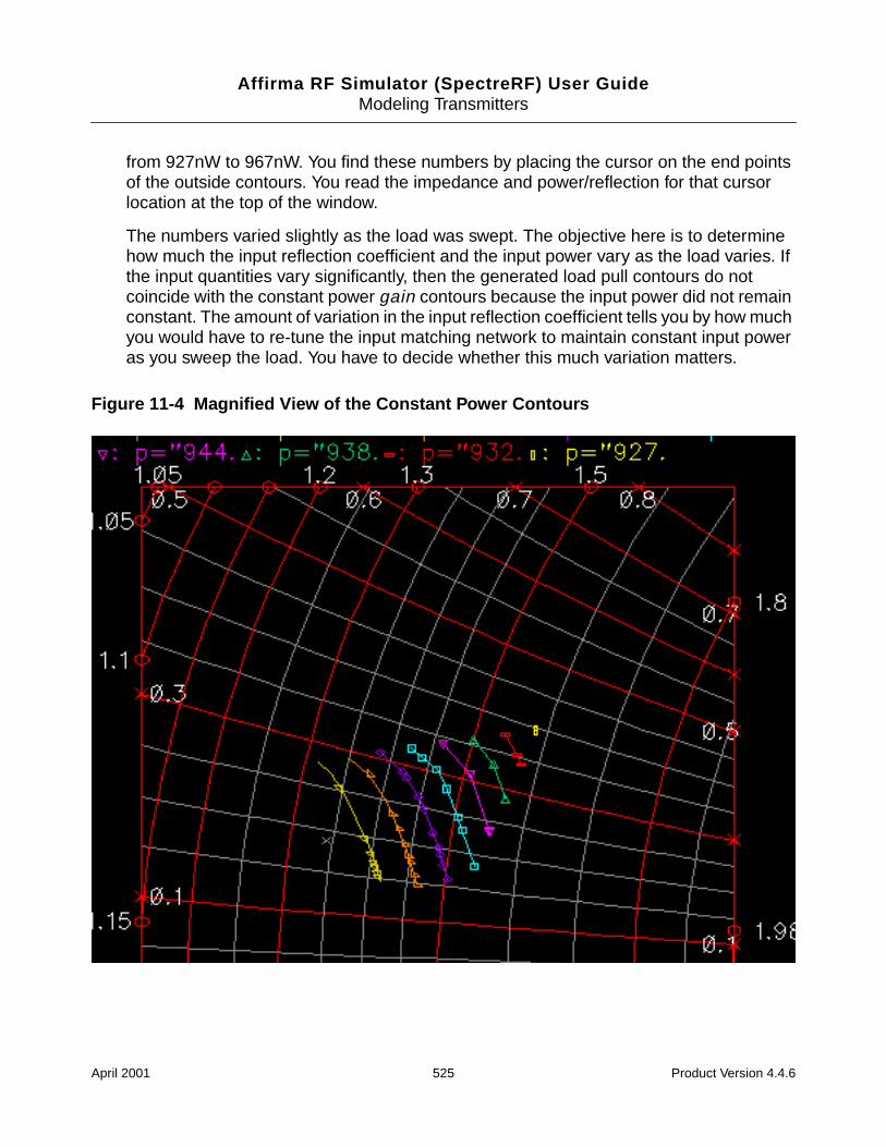
Affirma RF Simulator (SpectreRF) User GuideModeling Transmitters
from 927nW to 967nW. You find these numbers by placing the cursor on the end pointsof the outside contours. You read the impedance and power/reflection for that cursorlocation at the top of the window.
The numbers varied slightly as the load was swept. The objective here is to determinehow much the input reflection coefficient and the input power vary as the load varies. Ifthe input quantities vary significantly, then the generated load pull contours do notcoincide with the constant power gain contours because the input power did not remainconstant. The amount of variation in the input reflection coefficient tells you by how muchyou would have to re-tune the input matching network to maintain constant input poweras you sweep the load. You have to decide whether this much variation matters.
Figure 11-4 Magnified View of the Constant Power Contours
April 2001 525 Product Version 4.4.6
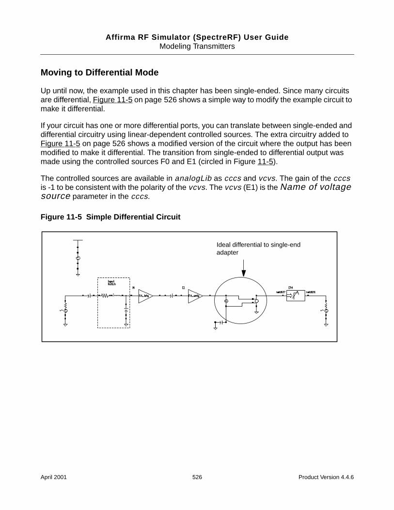
Affirma RF Simulator (SpectreRF) User GuideModeling Transmitters
Moving to Differential Mode
Up until now, the example used in this chapter has been single-ended. Since many circuitsare differential, Figure 11-5 on page 526 shows a simple way to modify the example circuit tomake it differential.
If your circuit has one or more differential ports, you can translate between single-ended anddifferential circuitry using linear-dependent controlled sources. The extra circuitry added toFigure 11-5 on page 526 shows a modified version of the circuit where the output has beenmodified to make it differential. The transition from single-ended to differential output wasmade using the controlled sources F0 and E1 (circled in Figure 11-5).
The controlled sources are available in analogLib as cccs and vcvs. The gain of the cccsis -1 to be consistent with the polarity of the vcvs. The vcvs (E1) is the Name of voltagesource parameter in the cccs.
Figure 11-5 Simple Differential Circuit
Ideal differential to single-endadapter
April 2001 526 Product Version 4.4.6
Affirma RF Simulator (SpectreRF) User GuideModeling Transmitters
Using S-Parameter Input Files
This example shows you how to create files of S-parameter data and how to specify ageneral n-port device in the frequency domain for a new simulation. In this example, thecreated S-parameter data file is entered back into the original circuit. It replaces that portionof the circuit used to create the S-parameters.
To enter tabulated S-parameters from some other source, simply record the data in the formatshown in this example and select the appropriate numerical options in the n-port.
To run a SpectreRF analysis that includes the new n-port, make sure you chose the rationalfitting option.
Setting Up the Schematic for the First Simulation
This example requires that you
Open the EF_example schematic.
Create a new cellview.
Copy part of the EF_example schematic and paste it in the new cellview.
Simulate the new cellview. This simulation generates the S-parameters of a linear time-invariant part of the original circuit. These S-parameters will be stored and used later toimport S-parameters into a simulation.
Opening the EF_example Schematic
1. Open and set up the EF_example schematic for simulation.
This is the same schematic that is used in the Envelope Following example of thischapter.
2. Leave the EF_example schematic open in the background.
Creating and Editing the New Cellview
1. In the CIW, choose File – New – Cellview….
The Create New File form appears.
April 2001 527 Product Version 4.4.6
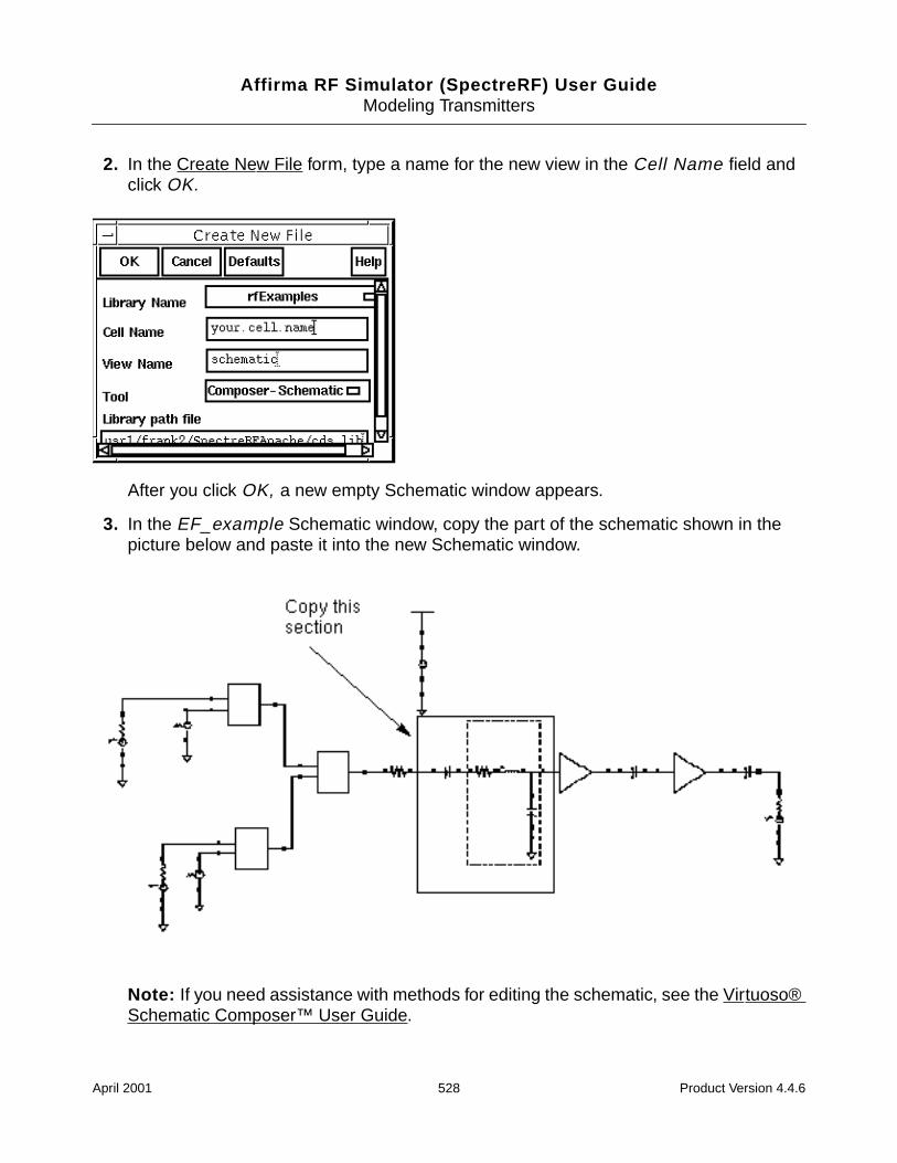
Affirma RF Simulator (SpectreRF) User GuideModeling Transmitters
2. In the Create New File form, type a name for the new view in the Cell Name field andclick OK.
After you click OK, a new empty Schematic window appears.
3. In the EF_example Schematic window, copy the part of the schematic shown in thepicture below and paste it into the new Schematic window.
Note: If you need assistance with methods for editing the schematic, see the Virtuoso®Schematic Composer™ User Guide.
April 2001 528 Product Version 4.4.6
Affirma RF Simulator (SpectreRF) User GuideModeling Transmitters
4. In the new Schematic window, choose Add – Instance….
The Add Instance form appears.
5. In the Add Instance form, click on Browse.
The Library Browser – Add Instance form appears.
6. Select the analogLib and highlight Show Categories.
7. In the Library Browser – Add Instance form, do the following:
a. Highlight Sources for Category.
b. In the Category list box, click on Sources.
The Category list box expands to display several subcategories under Sources.
c. Highlight the Ports subcategory under Sources.
d. Highlight port for Cell.
e. Highlight symbol for View.
April 2001 529 Product Version 4.4.6
Affirma RF Simulator (SpectreRF) User GuideModeling Transmitters
The form now looks like the one below:
8. Place two port symbols in the new Schematic window.
9. In the Library Browser – Add Instance form, do the following:
a. Highlight analogLib for Library.
b. Highlight Everything for Category.
c. Highlight gnd for Cell.
d. Highlight symbol for View.
10. Place two gnd components in the schematic.
April 2001 530 Product Version 4.4.6
Affirma RF Simulator (SpectreRF) User GuideModeling Transmitters
11. Wire up the components in the new Schematic window to make them look like this.
12. In the new Schematic window, choose Edit – Properties – Objects….
13. For each of the port components in the new schematic, do the following in the EditObject Properties form:
a. Select the port.
b. Type the appropriate number in the Port number field.
The diagram below tells you the appropriate number to type. Leave the Portresistances at their default of 50 Ohms.
April 2001 531 Product Version 4.4.6
Affirma RF Simulator (SpectreRF) User GuideModeling Transmitters
c. Click on Apply.
14. In the Edit Object Properties form, click OK.
15. In the new Schematic window, choose Design – Check and Save.
Setting Up and Running the First Simulation
1. In the new Schematic window, choose Tools – Analog Environment.
2. In the Simulation window, choose Analyses – Choose….
The Choosing Analyses form appears.
3. In the Choosing Analyses form, do the following:
a. Highlight sp for Analysis.
b. Highlight Frequency for Sweep Variable.
c. Highlight Start – Stop for Sweep Range.
d. Type 100K for Start and 10G for Stop.
e. Choose Automatic for Sweep Type.
f. Highlight no for Do Noise.
4. In the Choosing Analyses form, click on Options….
Port number=1 Portnumber=2
April 2001 532 Product Version 4.4.6
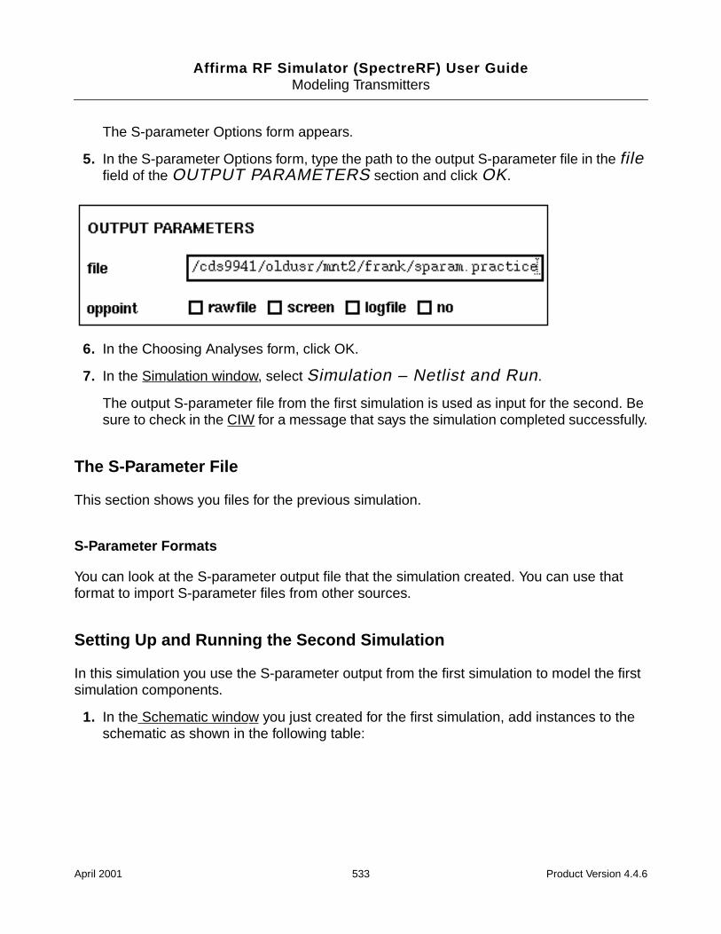
Affirma RF Simulator (SpectreRF) User GuideModeling Transmitters
The S-parameter Options form appears.
5. In the S-parameter Options form, type the path to the output S-parameter file in the filefield of the OUTPUT PARAMETERS section and click OK.
6. In the Choosing Analyses form, click OK.
7. In the Simulation window, select Simulation – Netlist and Run.
The output S-parameter file from the first simulation is used as input for the second. Besure to check in the CIW for a message that says the simulation completed successfully.
The S-Parameter File
This section shows you files for the previous simulation.
S-Parameter Formats
You can look at the S-parameter output file that the simulation created. You can use thatformat to import S-parameter files from other sources.
Setting Up and Running the Second Simulation
In this simulation you use the S-parameter output from the first simulation to model the firstsimulation components.
1. In the Schematic window you just created for the first simulation, add instances to theschematic as shown in the following table:
April 2001 533 Product Version 4.4.6
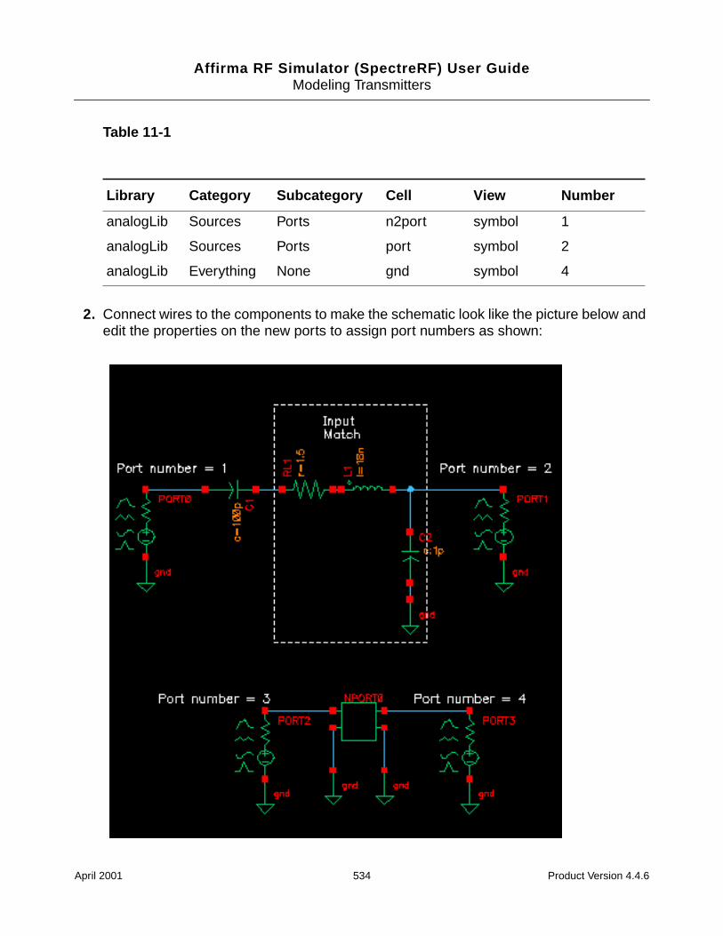
Affirma RF Simulator (SpectreRF) User GuideModeling Transmitters
Table 11-1
2. Connect wires to the components to make the schematic look like the picture below andedit the properties on the new ports to assign port numbers as shown:
Library Category Subcategory Cell View Number
analogLib Sources Ports n2port symbol 1
analogLib Sources Ports port symbol 2
analogLib Everything None gnd symbol 4
April 2001 534 Product Version 4.4.6
Affirma RF Simulator (SpectreRF) User GuideModeling Transmitters
3. In the Schematic window, select the n2port.
4. In the Edit Object Properties form, do the following and then click OK:
a. In the S-parameter data file field, type the absolute path to the S-parameterfile you created in the last simulation.
b. Choose rational for Interpolation method.
The form changes to let you add additional information.
c. Type .001 for Relative error.
d. Type 1e-6 for Absolute error.
e. Type 6 for Rational order.
This is mandatory if you plan to run SpectreRF.
April 2001 535 Product Version 4.4.6
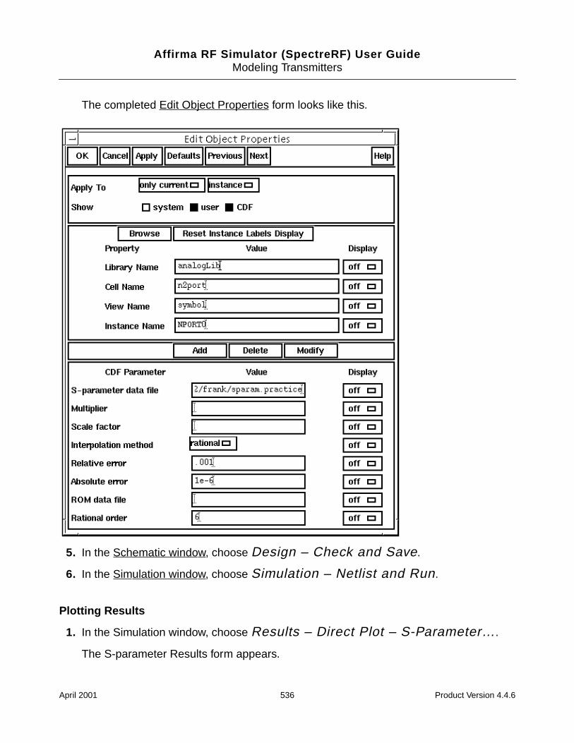
Affirma RF Simulator (SpectreRF) User GuideModeling Transmitters
The completed Edit Object Properties form looks like this.
5. In the Schematic window, choose Design – Check and Save.
6. In the Simulation window, choose Simulation – Netlist and Run.
Plotting Results
1. In the Simulation window, choose Results – Direct Plot – S-Parameter….
The S-parameter Results form appears.
April 2001 536 Product Version 4.4.6
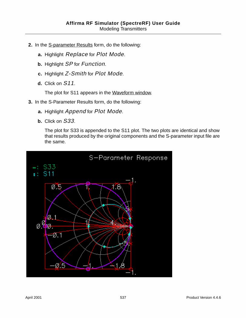
Affirma RF Simulator (SpectreRF) User GuideModeling Transmitters
2. In the S-parameter Results form, do the following:
a. Highlight Replace for Plot Mode.
b. Highlight SP for Function.
c. Highlight Z-Smith for Plot Mode.
d. Click on S11.
The plot for S11 appears in the Waveform window.
3. In the S-Parameter Results form, do the following:
a. Highlight Append for Plot Mode.
b. Click on S33.
The plot for S33 is appended to the S11 plot. The two plots are identical and showthat results produced by the original components and the S-parameter input file arethe same.
April 2001 537 Product Version 4.4.6
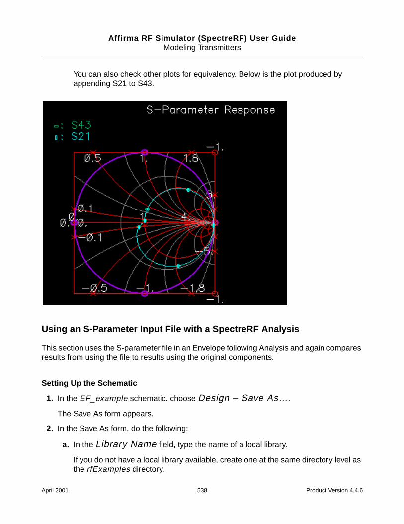
Affirma RF Simulator (SpectreRF) User GuideModeling Transmitters
You can also check other plots for equivalency. Below is the plot produced byappending S21 to S43.
Using an S-Parameter Input File with a SpectreRF Analysis
This section uses the S-parameter file in an Envelope following Analysis and again comparesresults from using the file to results using the original components.
Setting Up the Schematic
1. In the EF_example schematic. choose Design – Save As….
The Save As form appears.
2. In the Save As form, do the following:
a. In the Library Name field, type the name of a local library.
If you do not have a local library available, create one at the same directory level asthe rfExamples directory.
April 2001 538 Product Version 4.4.6
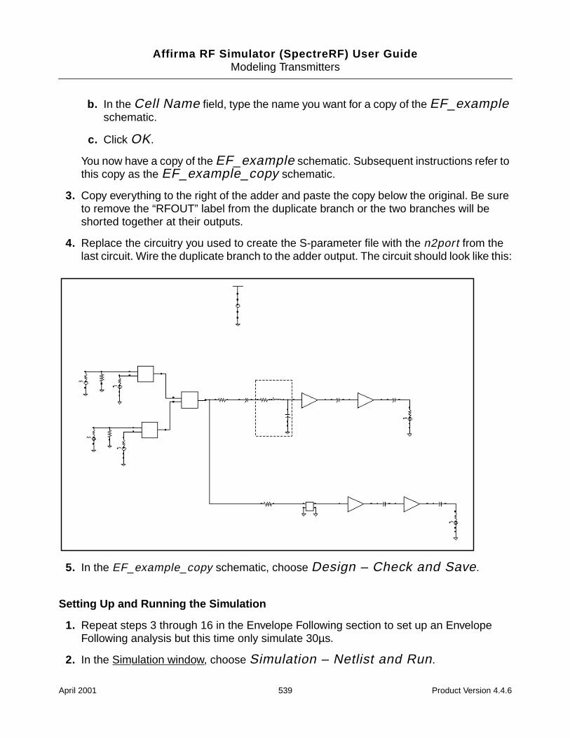
Affirma RF Simulator (SpectreRF) User GuideModeling Transmitters
b. In the Cell Name field, type the name you want for a copy of the EF_exampleschematic.
c. Click OK.
You now have a copy of the EF_example schematic. Subsequent instructions refer tothis copy as the EF_example_copy schematic.
3. Copy everything to the right of the adder and paste the copy below the original. Be sureto remove the “RFOUT” label from the duplicate branch or the two branches will beshorted together at their outputs.
4. Replace the circuitry you used to create the S-parameter file with the n2port from thelast circuit. Wire the duplicate branch to the adder output. The circuit should look like this:
5. In the EF_example_copy schematic, choose Design – Check and Save.
Setting Up and Running the Simulation
1. Repeat steps 3 through 16 in the Envelope Following section to set up an EnvelopeFollowing analysis but this time only simulate 30µs.
2. In the Simulation window, choose Simulation – Netlist and Run.
April 2001 539 Product Version 4.4.6
Affirma RF Simulator (SpectreRF) User GuideModeling Transmitters
Be sure to check the CIW for a message that says the simulation completed successfully.
Displaying the Results
1. In the Simulation window, choose Results – Direct Plot – ENVLP….
The Envelope Following Results form appears.
2. In the Envelope Following Results form, do the following:
a. Highlight Replace for Plot Mode.
b. Highlight Voltage for Function.
c. Highlight Real for Modifier.
d. Choose 1 for Harmonic Number.
April 2001 540 Product Version 4.4.6
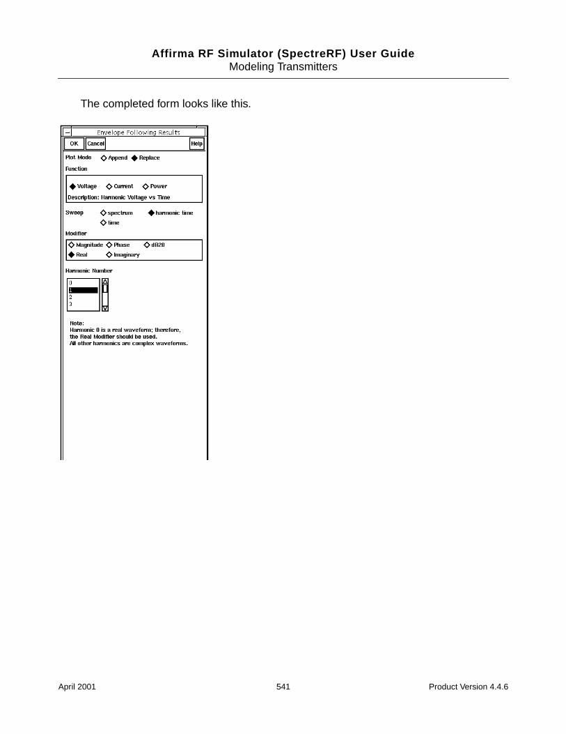
Affirma RF Simulator (SpectreRF) User GuideModeling Transmitters
The completed form looks like this.
April 2001 541 Product Version 4.4.6
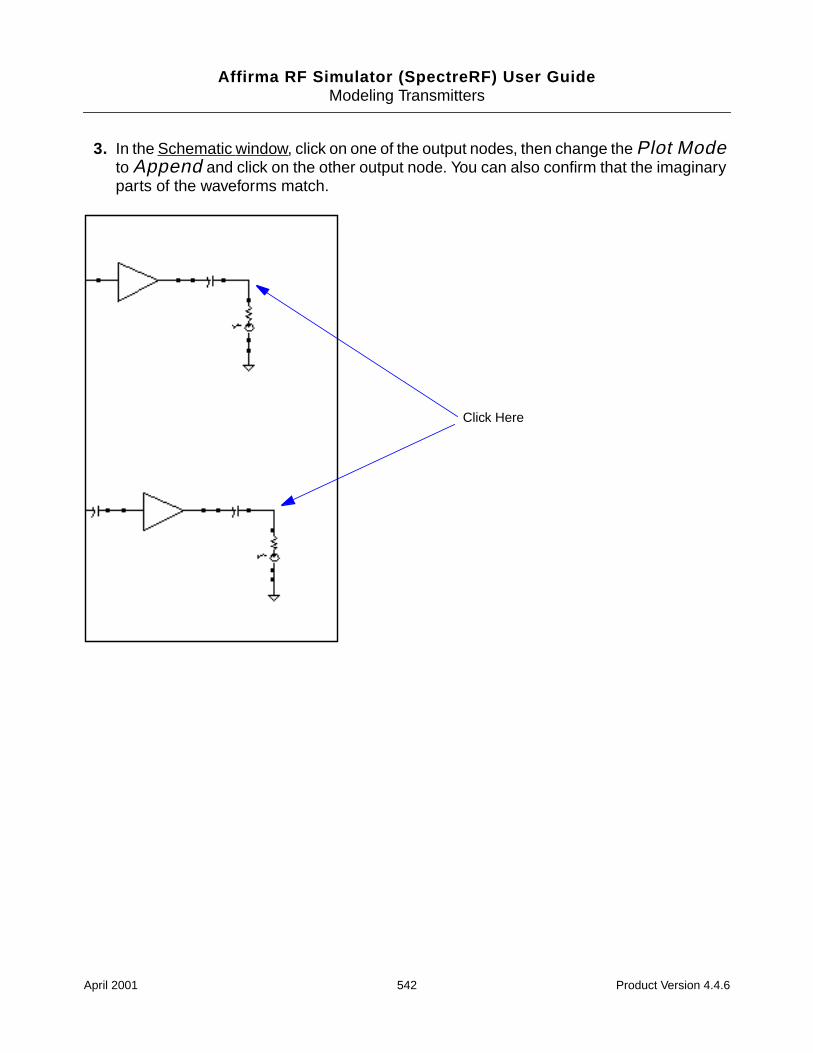
Affirma RF Simulator (SpectreRF) User GuideModeling Transmitters
3. In the Schematic window, click on one of the output nodes, then change the Plot Modeto Append and click on the other output node. You can also confirm that the imaginaryparts of the waveforms match.
Click Here
April 2001 542 Product Version 4.4.6
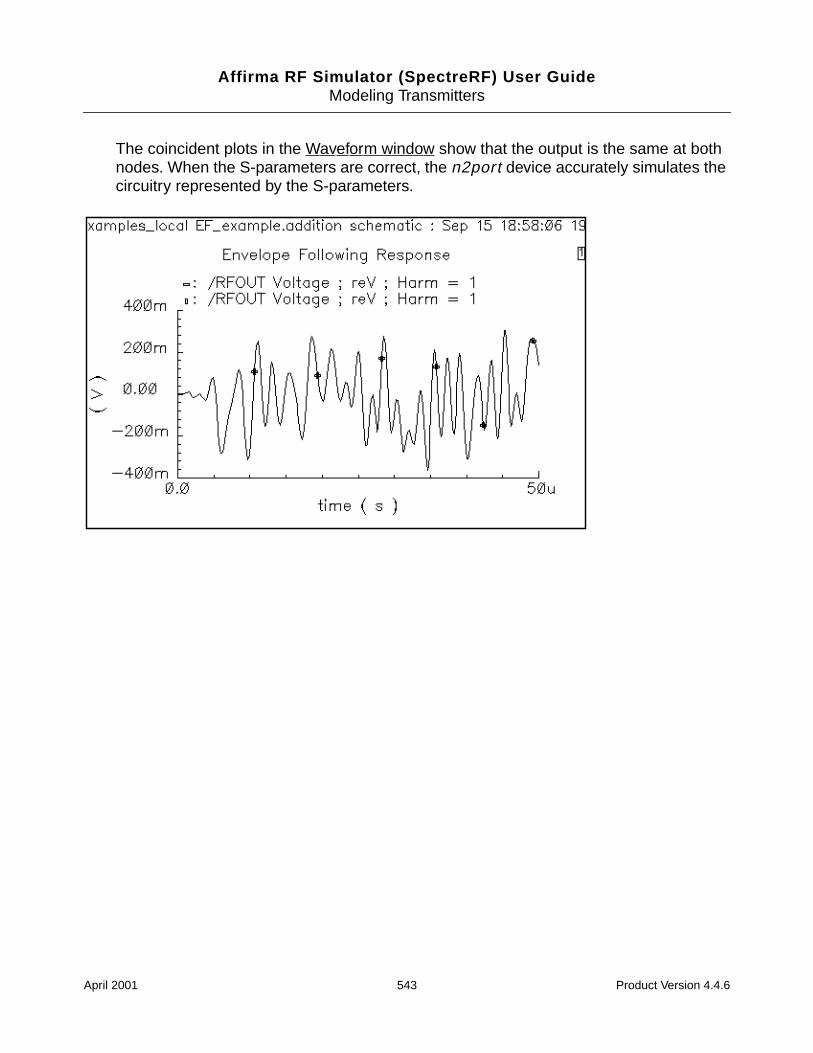
Affirma RF Simulator (SpectreRF) User GuideModeling Transmitters
The coincident plots in the Waveform window show that the output is the same at bothnodes. When the S-parameters are correct, the n2port device accurately simulates thecircuitry represented by the S-parameters.
April 2001 543 Product Version 4.4.6
Affirma RF Simulator (SpectreRF) User Guide
12Modeling Spiral Inductors and Bondpads
The procedures for modeling spiral inductors and bondpads are similar in many ways.
Modeling Spiral Inductors
The on-chip passive component modeler simulates spiral inductors, planar transformers, andbonding pads for RF applications. The modeler has an extraction engine based on EM(Electromagnetics) techniques. The Affirma analog circuit design environment calls thisengine using a command interface.
There are two use models for the modeler.
One use model is using the modeler in the schematic flow. You specify the inputparameters for the modeler in the CDF form, and model extraction is executed atnetlisting time.
The other use model is using the RF sub-menu option to access the modeler. You launchthe modeler directly using the Affirma analog circuit design environment Tools menu.The inductor model is extracted and written to the specific model directory, and theelectric parameters of the components are calculated and displayed on the UI form. Youcan include the extracted model in Spectre/SpectreRF simulations, with multipleinstances if necessary, and therefore avoid a long extraction time at netlisting.
The solver for the on-chip passive modeler employs a PEEC (Partial Element EquivalentCircuit) algorithm to generate macromodels for the spiral components. Electro-static andmagneto-static EM solvers are called separately to extract the capacitive and inductiveparameters of the structure.
The capacitive parameter extraction solver uses the BEM (Boundary Element Method), whichcomputes the lossy substrate using a complex Green’s function, and the solver is SVD(Singular Value Decomposition) accelerated.
The inductance solver is based on Fasthenry. It considers skin-depth effects, and models thesubstrate effect by treating the lossy layers as lossy conductor planes. The meshes forinductive and capacitive extractions are inter-correlated. There is one more segment for
April 2001 544 Product Version 4.4.6
Affirma RF Simulator (SpectreRF) User GuideModeling Spiral Inductors and Bondpads
capacitive extraction than there is for the inductive mesh. There is also a half segment overlapbetween the two meshes. Because of the conductor and substrate loss, the extractedparameters are formulated as RLGC matrices.
With the extracted parameters, a multi-PI equivalent circuit is created. Depending on thebandwidth, the modeler generates either a narrow-bandwidth or wide-bandwidth model.
The narrow-bandwidth model uses the parasitic parameters extracted at the workingfrequency and builds a fully-coupled multi-PI equivalent circuit. Because the capacitive andinductive parameters are functions of frequency, this model is accurate only in the vicinity ofthe working frequency specified. The wide-bandwidth model extracts the capacitive andinductive parameters over a wide frequency range, and generates a model as an nport. In thenport, a ratio of rational polynomials represents the frequency dependent behavior. Unlike thenarrow-bandwidth model, the wide-bandwidth model is accurate over the whole frequencyrange up to the specified maximum frequency of interest. However, the model extractiontakes longer, and in some cases, the extracted model might not be passive and might causesimulation failure. If the simulation fails, the solver automatically switches to a narrow-bandwidth model.
The remainder of the spiral inductor section covers the following topics:
The Process File Preparation section explains how to setup the process file and gives anexample CMOS process file.
The Spiral Inductor Simulation in the Schematic Flow section explains details about thespiral inductor symbol and CDF parameters.
The Spiral Inductor Modeling Using the RF Sub-menu section tells you how to model aspiral inductor using the RF sub-menu and explains the electrical parameters.
The Equivalent Circuit Models section explains the equivalent circuit models anddiscusses issues you need to be aware of.
The Example section takes you step-by-step through a simulation that uses the spiralinductor modeling capability.
Process File Preparation
Before you use the passive modeler, you must create a process file that contains the layerinformation for both the metal and the substrate.
In the current release, you must hand edit the file to conform exactly to the required format.
April 2001 545 Product Version 4.4.6
Affirma RF Simulator (SpectreRF) User GuideModeling Spiral Inductors and Bondpads
File Format
The process file is in the following format
processType type
numLayers # of layers
layerInfo 0
...
layerInfo # of layers-1
In the above format, the first line, processType, is currently used only for documentation. Thesecond line specifies the number of layers, including both the dielectric and metal layers. Thefollowing lines are Nl blocks of layer information. Each layer information block has a specificformat you must follow.
In the process file, all separate structures are modeled so as to account for the effects ofsurrounding layers. For example, a two-metal layer structure immersed in the substrate ismodeled as five different layers: the dielectric layer underneath the bottom metal layer, thebottom metal layer, the dielectric layer between the two metal layers, the top metal layer, andthe layer above the top metal layer.
Layer Information Format
You can specify the following three types of layers:
ground plane – The whole layer is a piece of metal.
dielectric – The whole layer is dielectric of uniform dielectric constant,
metal layer – Part of the structure is metal surrounded by dielectric.
The formats for these three layer types are shown below:
Format for the ground plane:
layer 0
name tab
type ground
thickness 0.1e-6
epsr 1
rho 1.7857e-8
April 2001 546 Product Version 4.4.6
Affirma RF Simulator (SpectreRF) User GuideModeling Spiral Inductors and Bondpads
Format for the dielectric layer:
layer 1
name substrate
type dielectric
thickness 300e-6
epsr 11.9
rho 0.1
Format for the metal layer:
layer 3
name metal1
type metal
thickness 1e-6
epsr 4
rho 1e10
rhom 3e-8
For the metal layer, rho is the resistivity of the dielectric surrounding the metal structure, andrhom is the resistivity of the metals. All the units must be in MKS.
Sample CMOS Process File
The following example shows a process file for a CMOS process as shown in Figure 12-1 onpage 549.
*Sample process file. All layers are stacked from bottom up
processType CMOS
numLayers 7
layer 0
name tab
type ground
thickness 0.1e-6
epsr 1
rho 1.7857e-8
layer 1
name substrate
type dielectric
thickness 300e-6
epsr 11.9
rho 0.1
layer 2
April 2001 547 Product Version 4.4.6
Affirma RF Simulator (SpectreRF) User GuideModeling Spiral Inductors and Bondpads
name sio2
type dielectric
thickness 1.5e-6
epsr 4.0
rho 1e10
layer 3
name metal1
type metal
thickness 1e-6
epsr 4
rho 1e10
rhom 3e-8
layer 4
name sio2
type dielectric
thickness 1.5e-6
epsr 4
rho 1e10
layer 5
name metal2
type metal
thickness 1e-6
epsr 4
rho 1e10
rhom 3e-8
layer 6
name sio2
type dielectric
thickness 43.5e-6
epsr 4
rho 1e10
April 2001 548 Product Version 4.4.6
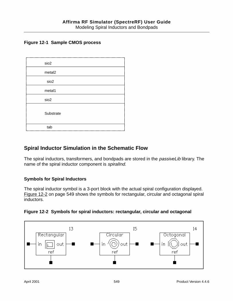
Affirma RF Simulator (SpectreRF) User GuideModeling Spiral Inductors and Bondpads
Figure 12-1 Sample CMOS process
Spiral Inductor Simulation in the Schematic Flow
The spiral inductors, transformers, and bondpads are stored in the passiveLib library. Thename of the spiral inductor component is spiralInd.
Symbols for Spiral Inductors
The spiral inductor symbol is a 3-port block with the actual spiral configuration displayed.Figure 12-2 on page 549 shows the symbols for rectangular, circular and octagonal spiralinductors.
Figure 12-2 Symbols for spiral inductors: rectangular, circular and octagonal
tab
Substrate
sio2
metal1
sio2
metal2
sio2
April 2001 549 Product Version 4.4.6
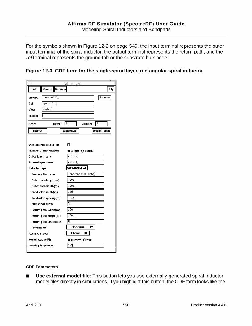
Affirma RF Simulator (SpectreRF) User GuideModeling Spiral Inductors and Bondpads
For the symbols shown in Figure 12-2 on page 549, the input terminal represents the outerinput terminal of the spiral inductor, the output terminal represents the return path, and theref terminal represents the ground tab or the substrate bulk node.
Figure 12-3 CDF form for the single-spiral layer, rectangular spiral inductor
CDF Parameters
Use external model file : This button lets you use externally-generated spiral-inductormodel files directly in simulations. If you highlight this button, the CDF form looks like the
April 2001 550 Product Version 4.4.6
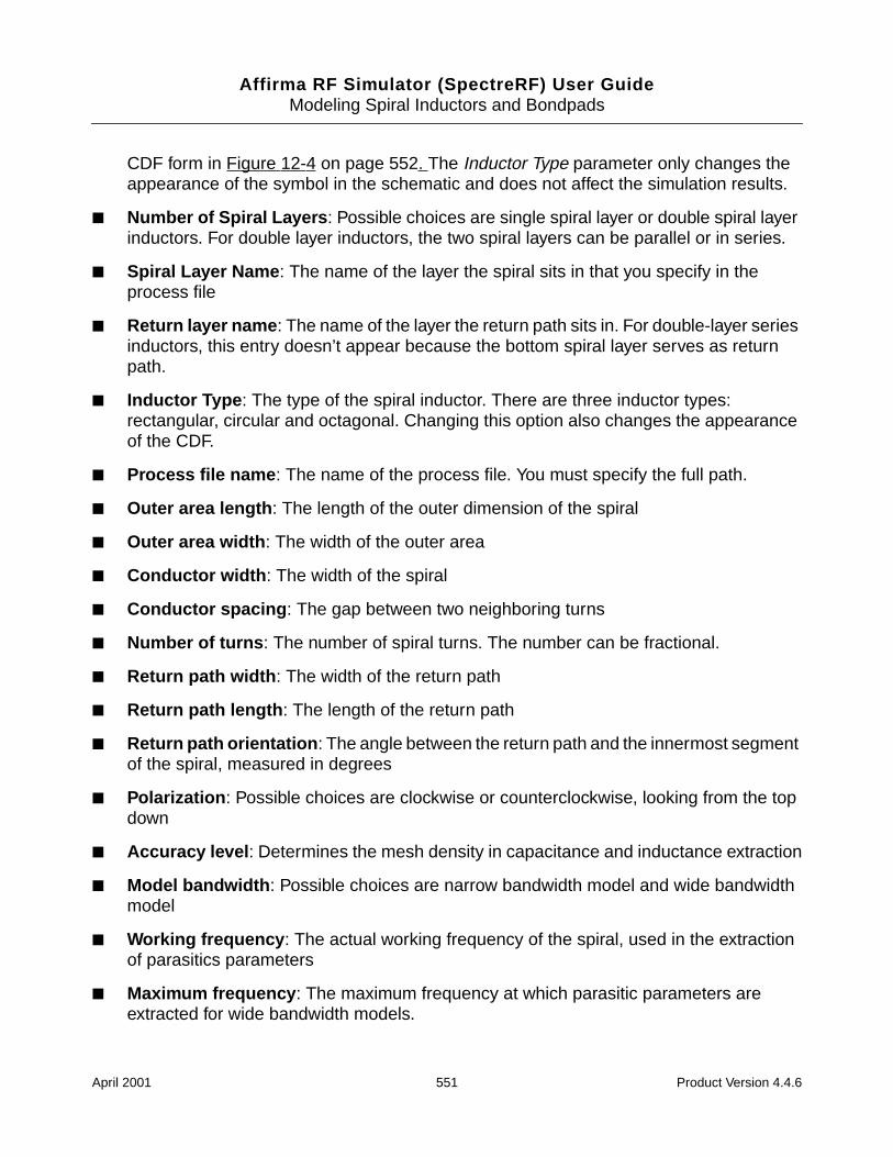
Affirma RF Simulator (SpectreRF) User GuideModeling Spiral Inductors and Bondpads
CDF form in Figure 12-4 on page 552. The Inductor Type parameter only changes theappearance of the symbol in the schematic and does not affect the simulation results.
Number of Spiral Layers : Possible choices are single spiral layer or double spiral layerinductors. For double layer inductors, the two spiral layers can be parallel or in series.
Spiral Layer Name : The name of the layer the spiral sits in that you specify in theprocess file
Return layer name : The name of the layer the return path sits in. For double-layer seriesinductors, this entry doesn’t appear because the bottom spiral layer serves as returnpath.
Inductor Type : The type of the spiral inductor. There are three inductor types:rectangular, circular and octagonal. Changing this option also changes the appearanceof the CDF.
Process file name : The name of the process file. You must specify the full path.
Outer area length : The length of the outer dimension of the spiral
Outer area width : The width of the outer area
Conductor width : The width of the spiral
Conductor spacing : The gap between two neighboring turns
Number of turns : The number of spiral turns. The number can be fractional.
Return path width : The width of the return path
Return path length : The length of the return path
Return path orientation : The angle between the return path and the innermost segmentof the spiral, measured in degrees
Polarization : Possible choices are clockwise or counterclockwise, looking from the topdown
Accuracy level : Determines the mesh density in capacitance and inductance extraction
Model bandwidth : Possible choices are narrow bandwidth model and wide bandwidthmodel
Working frequency : The actual working frequency of the spiral, used in the extractionof parasitics parameters
Maximum frequency : The maximum frequency at which parasitic parameters areextracted for wide bandwidth models.
April 2001 551 Product Version 4.4.6
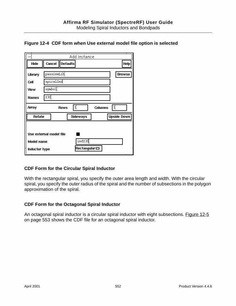
Affirma RF Simulator (SpectreRF) User GuideModeling Spiral Inductors and Bondpads
Figure 12-4 CDF form when Use external model file option is selected
CDF Form for the Circular Spiral Inductor
With the rectangular spiral, you specify the outer area length and width. With the circularspiral, you specify the outer radius of the spiral and the number of subsections in the polygonapproximation of the spiral.
CDF Form for the Octagonal Spiral Inductor
An octagonal spiral inductor is a circular spiral inductor with eight subsections. Figure 12-5on page 553 shows the CDF file for an octagonal spiral inductor.
April 2001 552 Product Version 4.4.6
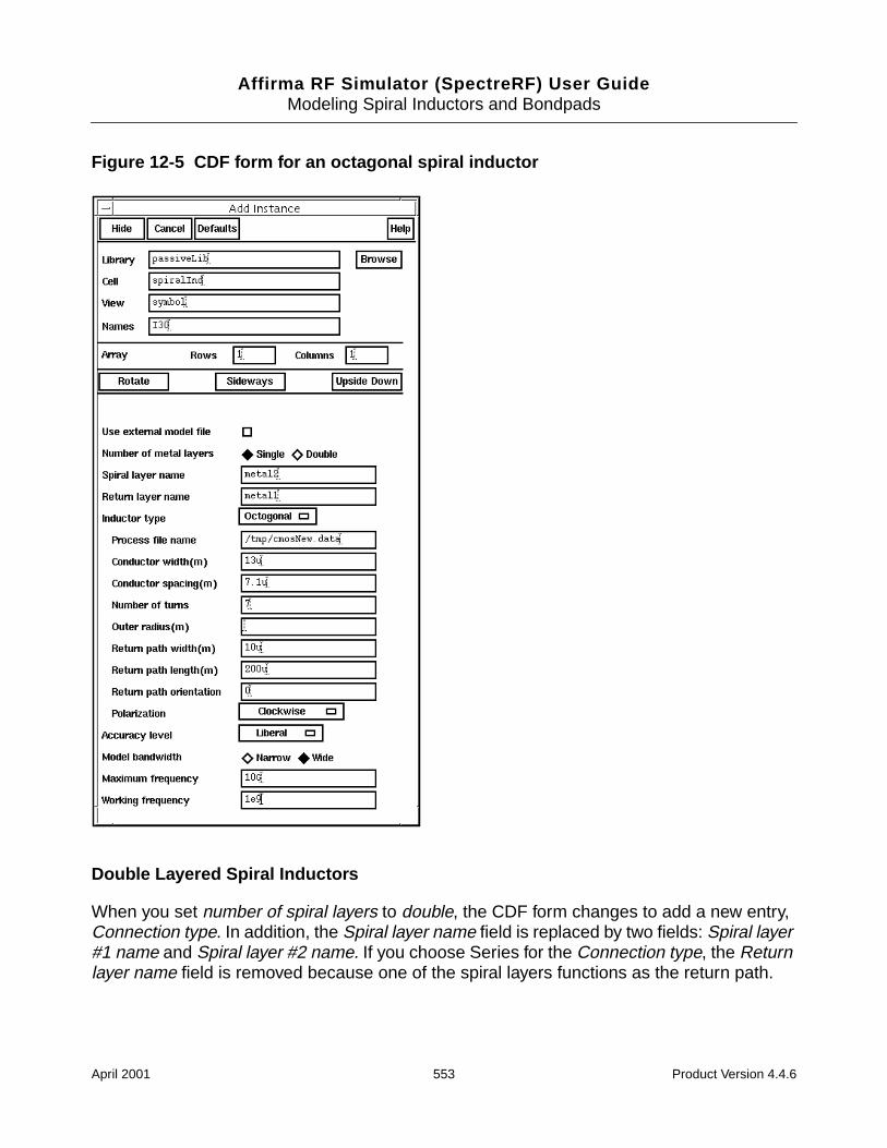
Affirma RF Simulator (SpectreRF) User GuideModeling Spiral Inductors and Bondpads
Figure 12-5 CDF form for an octagonal spiral inductor
Double Layered Spiral Inductors
When you set number of spiral layers to double, the CDF form changes to add a new entry,Connection type. In addition, the Spiral layer name field is replaced by two fields: Spiral layer#1 name and Spiral layer #2 name. If you choose Series for the Connection type, the Returnlayer name field is removed because one of the spiral layers functions as the return path.
April 2001 553 Product Version 4.4.6
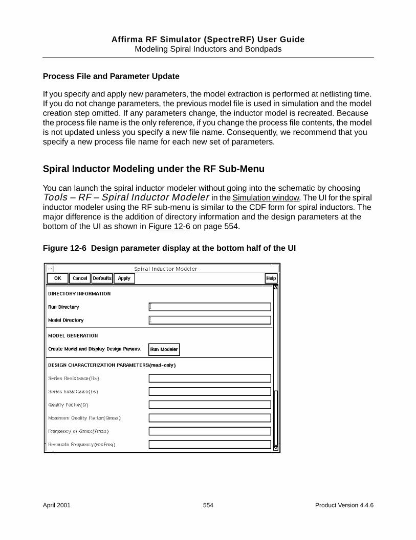
Affirma RF Simulator (SpectreRF) User GuideModeling Spiral Inductors and Bondpads
Process File and Parameter Update
If you specify and apply new parameters, the model extraction is performed at netlisting time.If you do not change parameters, the previous model file is used in simulation and the modelcreation step omitted. If any parameters change, the inductor model is recreated. Becausethe process file name is the only reference, if you change the process file contents, the modelis not updated unless you specify a new file name. Consequently, we recommend that youspecify a new process file name for each new set of parameters.
Spiral Inductor Modeling under the RF Sub-Menu
You can launch the spiral inductor modeler without going into the schematic by choosingTools – RF – Spiral Inductor Modeler in the Simulation window. The UI for the spiralinductor modeler using the RF sub-menu is similar to the CDF form for spiral inductors. Themajor difference is the addition of directory information and the design parameters at thebottom of the UI as shown in Figure 12-6 on page 554.
Figure 12-6 Design parameter display at the bottom half of the UI
April 2001 554 Product Version 4.4.6
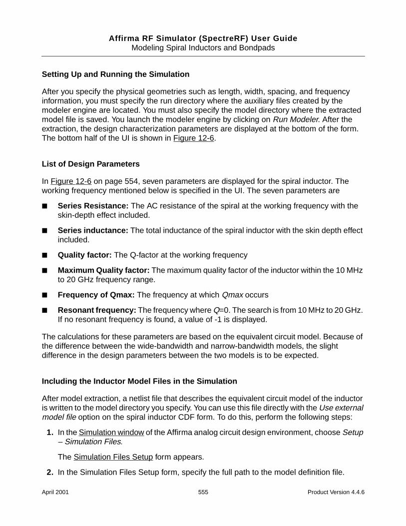
Affirma RF Simulator (SpectreRF) User GuideModeling Spiral Inductors and Bondpads
Setting Up and Running the Simulation
After you specify the physical geometries such as length, width, spacing, and frequencyinformation, you must specify the run directory where the auxiliary files created by themodeler engine are located. You must also specify the model directory where the extractedmodel file is saved. You launch the modeler engine by clicking on Run Modeler. After theextraction, the design characterization parameters are displayed at the bottom of the form.The bottom half of the UI is shown in Figure 12-6.
List of Design Parameters
In Figure 12-6 on page 554, seven parameters are displayed for the spiral inductor. Theworking frequency mentioned below is specified in the UI. The seven parameters are
Series Resistance: The AC resistance of the spiral at the working frequency with theskin-depth effect included.
Series inductance: The total inductance of the spiral inductor with the skin depth effectincluded.
Quality factor: The Q-factor at the working frequency
Maximum Quality factor: The maximum quality factor of the inductor within the 10 MHzto 20 GHz frequency range.
Frequency of Qmax: The frequency at which Qmax occurs
Resonant frequency: The frequency where Q=0. The search is from 10 MHz to 20 GHz.If no resonant frequency is found, a value of -1 is displayed.
The calculations for these parameters are based on the equivalent circuit model. Because ofthe difference between the wide-bandwidth and narrow-bandwidth models, the slightdifference in the design parameters between the two models is to be expected.
Including the Inductor Model Files in the Simulation
After model extraction, a netlist file that describes the equivalent circuit model of the inductoris written to the model directory you specify. You can use this file directly with the Use externalmodel file option on the spiral inductor CDF form. To do this, perform the following steps:
1. In the Simulation window of the Affirma analog circuit design environment, choose Setup– Simulation Files.
The Simulation Files Setup form appears.
2. In the Simulation Files Setup form, specify the full path to the model definition file.
April 2001 555 Product Version 4.4.6
Affirma RF Simulator (SpectreRF) User GuideModeling Spiral Inductors and Bondpads
Equivalent Circuit Models
This section discusses the two types of equivalent circuit models:
Narrow bandwidth model
Wide bandwidth model
Narrow Bandwidth Model
This narrow bandwidth model, as shown in Figure 12-7 on page 556, is constructed directlyfrom the RLGC matrices obtained at the working frequency. All the elements are fully coupledthrough capacitors and inductors.
Figure 12-7 Narrow-bandwidth model for a spiral inductor
Because the RLGC parameters are functions of frequency, the above model is valid only inthe vicinity of the working frequency. It is therefore a narrow-bandwidth model. Expect largesimulation error for frequency components outside of the bandwidth. Because this model onlyrequires the extraction of RLCG parameters at a single frequency, the extraction is faster. Theresulting model is also guaranteed to be passive and stable.
Equivalent Circuit Order
The number of PIs in the equivalent circuit depends on the number of turns in the spiralinductor. For single-spiral layer inductors and the double-spiral layer with parallel connectioninductors, the number of PIs equals the number of turns. For double spiral layer with seriesconnection inductors, the number of PIs equals twice the number of turns.
...
April 2001 556 Product Version 4.4.6
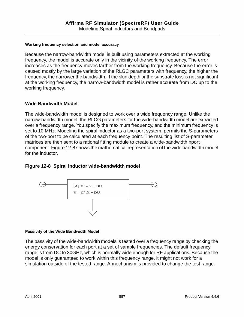
Affirma RF Simulator (SpectreRF) User GuideModeling Spiral Inductors and Bondpads
Working frequency selection and model accuracy
Because the narrow-bandwidth model is built using parameters extracted at the workingfrequency, the model is accurate only in the vicinity of the working frequency. The errorincreases as the frequency moves farther from the working frequency. Because the error iscaused mostly by the large variation of the RLGC parameters with frequency, the higher thefrequency, the narrower the bandwidth. If the skin depth or the substrate loss is not significantat the working frequency, the narrow-bandwidth model is rather accurate from DC up to theworking frequency.
Wide Bandwidth Model
The wide-bandwidth model is designed to work over a wide frequency range. Unlike thenarrow-bandwidth model, the RLCG parameters for the wide-bandwidth model are extractedover a frequency range. You specify the maximum frequency, and the minimum frequency isset to 10 MHz. Modeling the spiral inductor as a two-port system, permits the S-parametersof the two-port to be calculated at each frequency point. The resulting list of S-parametermatrices are then sent to a rational fitting module to create a wide-bandwidth nportcomponent. Figure 12-8 shows the mathematical representation of the wide bandwidth modelfor the inductor.
Figure 12-8 Spiral inductor wide-bandwidth model
Passivity of the Wide Bandwidth Model
The passivity of the wide-bandwidth models is tested over a frequency range by checking theenergy conservation for each port at a set of sample frequencies. The default frequencyrange is from DC to 30GHz, which is normally wide enough for RF applications. Because themodel is only guaranteed to work within this frequency range, it might not work for asimulation outside of the tested range. A mechanism is provided to change the test range.
[A] X’ = X + BU
Y = C^tX + DU
April 2001 557 Product Version 4.4.6
Affirma RF Simulator (SpectreRF) User GuideModeling Spiral Inductors and Bondpads
Set maximum Frequency for Passivity Check
You can reset the maximum frequency for the passivity checking by setting the environmentvariable maxFreqForPassivityTest.
setenv maxFreqForPassivityTest 50e9
Automatic Model Switch
To avoid simulation failure caused by non-passivity of the wide-bandwidth model, the modelerautomatically switches to a narrow-bandwidth model if the passivity test fails. You can preventthis automatic switching by setting an environment variable in the window where you starticms.
setenv pcmModelAutoSwitch OFF
If you turn off the switch, the wide-bandwidth model is created and a warning messageissued. Spectre uses the model in simulation even though it is not passive.
Accuracy Analysis
The Accuracy level entry on both the CDF and the RF sub-menu UI forms controls the meshdensity for both the capacitance and inductance extraction. For capacitance, the number ofsubsections per width is three, five, or seven. These values correspond to the Liberal,Moderate and Conservative accuracy levels. Inductance calculation is similarly correlatedwith the accuracy level. Three, five, or seven filaments are used in the transverse direction tothe current, corresponding to the three accuracy levels. The error is less than 3% at theLiberal level, and about 1% at the Conservative level.
April 2001 558 Product Version 4.4.6
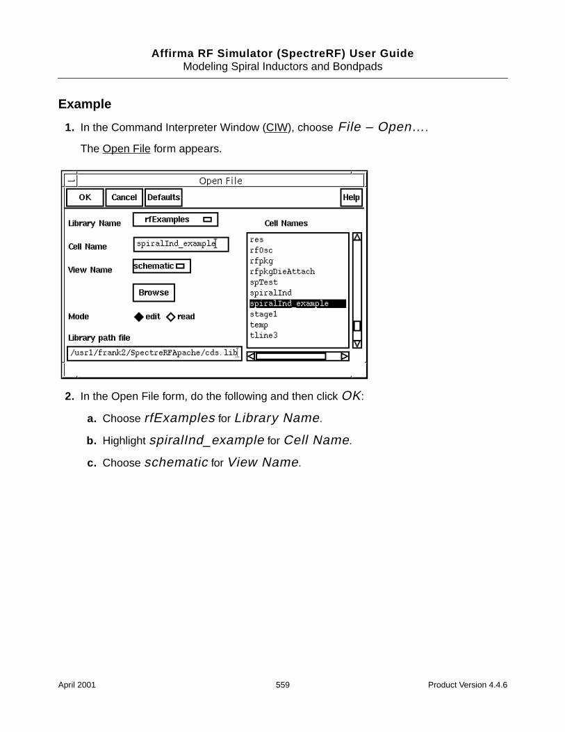
Affirma RF Simulator (SpectreRF) User GuideModeling Spiral Inductors and Bondpads
Example
1. In the Command Interpreter Window (CIW), choose File – Open….
The Open File form appears.
2. In the Open File form, do the following and then click OK:
a. Choose rfExamples for Library Name.
b. Highlight spiralInd_example for Cell Name.
c. Choose schematic for View Name.
April 2001 559 Product Version 4.4.6
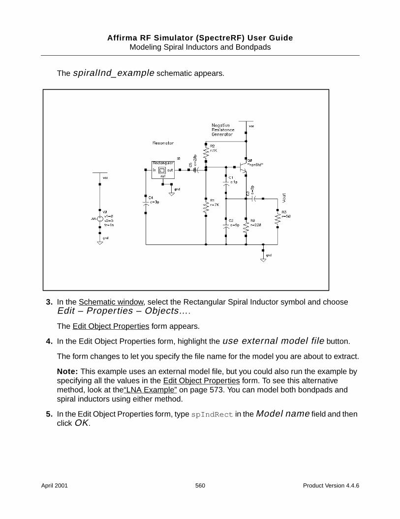
Affirma RF Simulator (SpectreRF) User GuideModeling Spiral Inductors and Bondpads
The spiralInd_example schematic appears.
3. In the Schematic window, select the Rectangular Spiral Inductor symbol and chooseEdit – Properties – Objects….
The Edit Object Properties form appears.
4. In the Edit Object Properties form, highlight the use external model file button.
The form changes to let you specify the file name for the model you are about to extract.
Note: This example uses an external model file, but you could also run the example byspecifying all the values in the Edit Object Properties form. To see this alternativemethod, look at the“LNA Example” on page 573. You can model both bondpads andspiral inductors using either method.
5. In the Edit Object Properties form, type spIndRect in the Model name field and thenclick OK.
April 2001 560 Product Version 4.4.6
Affirma RF Simulator (SpectreRF) User GuideModeling Spiral Inductors and Bondpads
The completed form looks like this.
6. In the Schematic window, choose Tools – Analog Environment….
April 2001 561 Product Version 4.4.6
Affirma RF Simulator (SpectreRF) User GuideModeling Spiral Inductors and Bondpads
The Simulation window appears.
7. In the Simulation window, choose Setup – Model Libraries….
The Model Library Setup form appears.
8. In the Model Library Setup form, do the following and then click OK.
a. In the Model Library File field, type the path to the npnStd.m file and thespIndRect.scs file.
$CDSHOME/tools/dfII/samples/artist/rfExamples/spiralInd_example/npnStd.m
/home/belinda/Spiral/InductorWork/spIndRect.scs
The npnStd.m file is in the spiralInd_example directory in the rfExamples library.
The spIndRect.scs file path points to the run directory where you want theextracted model file to be written.
b. Click on Add after you specify each file.
April 2001 562 Product Version 4.4.6
Affirma RF Simulator (SpectreRF) User GuideModeling Spiral Inductors and Bondpads
The completed form looks like the one below.
9. In the Simulation window, choose Tools – RF – Spiral Inductor Modeler….
The Spiral Inductor Modeler form appears.
10. In the Spiral Inductor Modeler form, do the following:
a. Highlight One for Number of metal layers.
b. Type metal1 for Spiral layer #1 name.
c. Type metal2 for Return layer name.
d. Choose Rectangular for Inductor type.
e. In the Process file name field, type the path to the cmos.data file.
$CDSHOME/tools/dfII/samples/artist/rfExamples/spiralInd_example/cmos.data
The cmos.data file is in the spiralInd_example directory in the rfExampleslibrary.
f. Type 300u for Outer area length(m).
g. Type 300u for Outer area width(m).
h. Type 10u for Conductor width(m).
April 2001 563 Product Version 4.4.6
Affirma RF Simulator (SpectreRF) User GuideModeling Spiral Inductors and Bondpads
i. Type 7u for Conductor spacing(m).
j. Type 7 for Number of turns.
k. Type 13u for Return path width(m).
l. Type 110u for Return path length(m).
m. Type -90 for Return path orientation.
n. Choose Clockwise for Polarization.
o. Choose Liberal for Accuracy level.
p. In the Model Name field, type the name that you choose for the model,spIndRect .
q. Highlight Narrow for Model bandwidth.
r. Type 1.5G for Working frequency.
s. In the Run Directory field, type the full path to the run directory.
/home/belinda/Spiral/InductorWork
t. In the Model Directory field, type the full path to the model you are creating.
/home/belinda/Spiral/InductorWork
The completed form looks like the following two illustrations:
April 2001 564 Product Version 4.4.6
Affirma RF Simulator (SpectreRF) User GuideModeling Spiral Inductors and Bondpads
Top part of the Spiral Inductor Modeler Form
April 2001 565 Product Version 4.4.6
Affirma RF Simulator (SpectreRF) User GuideModeling Spiral Inductors and Bondpads
Bottom Part of the Spiral Inductor Model Form
11. Click on the Run Modeler button adjacent to Create Model and DisplayDesign Params.
April 2001 566 Product Version 4.4.6
Affirma RF Simulator (SpectreRF) User GuideModeling Spiral Inductors and Bondpads
The model is created. When the process is completed, the calculated parameters aredisplayed in a read-only fields at the bottom of the Spiral Inductor Modeler form.
12. In the Simulation window, choose Outputs – To Be Plotted – Select OnSchematic.
13. In the Schematic window, click on the Vout node.
14. In the Simulation window, choose Analyses – Choose….
The Choosing Analyses form appears.
15. In the Choosing Analyses form, do the following and then click OK:
Click here
April 2001 567 Product Version 4.4.6
Affirma RF Simulator (SpectreRF) User GuideModeling Spiral Inductors and Bondpads
a. Highlight tran for Analysis.
b. Type 200n for Stop Time.
c. Highlight Enabled.
16. In the Simulation window, choose Simulation – Netlist and Run.
The simulation runs. When the simulation completes, the Waveform window appearswith the plot for the example.
April 2001 568 Product Version 4.4.6
Affirma RF Simulator (SpectreRF) User GuideModeling Spiral Inductors and Bondpads
Modeling Bondpads
On-chip passive components, especially those on lossy substrate and operating at highfrequencies, need careful modeling. Bonding pads are the interface between the chip andoutside world, and their behavior significantly affects circuit performance. The core algorithmsused in bonding pads are also used in the capacitance extraction for spiral inductor modeling.
Capacitive coupling, appearing as capacitance and resistance caused by displacementcurrent, normally is modeled in high-frequency or high-speed applications because itscoupling characteristics. This displacement current is different from inductive current that arecharacterized by inductance. Accurate extraction of these coupling effects, however, requiressolving Poisson’s equation and becomes computation-intensive. For lossy substrate, whencapacitive coupling and resistive coupling are of the same order of magnitude, the frequency-dependent effects require additional extraction efforts. This bonding pad model uses thecomplex multilayered Green’s function [2] to capture capacitive couplings and lossinformation. It uses IES3[1] to accelerate its computation and further uses a novel techniqueto fit the frequency-dependent data. Because of this technique, you can perform PSSanalysis as well as all the conventional circuit analyses.
You do not have to start the modeling tool manually. Instead, you place the symbol of thebonding pads into your schematic design. You can change the CDF parameters (theparameters that associate with the model) to reflect a design. If you netlist a circuit before thesimulation, the extraction tool is automatically invoked and added or changed parameters areinserted into the netlist. You can also generate the model using the RF submenu in theAffirma analog circuit design environment. This approach only generates the internal modelcalled ROM (reduced order model) that is stored in a file. You can use this file in CDF form toavoid unnecessarily generating the model during netlisting. The model is only generatedduring netlisting procedure when the model is new or the parameters are changed.
The current fitting algorithm still has not completely solved the passivity problem. Rarely, anon-passive model might cause simulation failure because of strong positive feedback withina circuit (such as an oscillator). When this happens, you can use a narrow-band model thatis accurate at the specified working frequency.
The data flow for using and modeling the bonding pad is shown in Figure 12-9 on page 570.
April 2001 569 Product Version 4.4.6
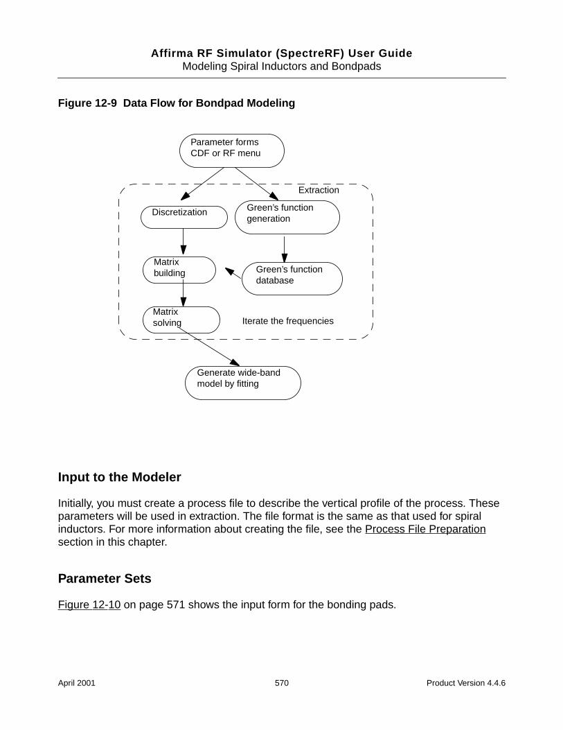
Affirma RF Simulator (SpectreRF) User GuideModeling Spiral Inductors and Bondpads
Figure 12-9 Data Flow for Bondpad Modeling
Input to the Modeler
Initially, you must create a process file to describe the vertical profile of the process. Theseparameters will be used in extraction. The file format is the same as that used for spiralinductors. For more information about creating the file, see the Process File Preparationsection in this chapter.
Parameter Sets
Figure 12-10 on page 571 shows the input form for the bonding pads.
Parameter formsCDF or RF menu
Discretization
Matrixbuilding
Matrixsolving
Green’s functiongeneration
Green’s functiondatabase
Extraction
Iterate the frequencies
Generate wide-bandmodel by fitting
April 2001 570 Product Version 4.4.6
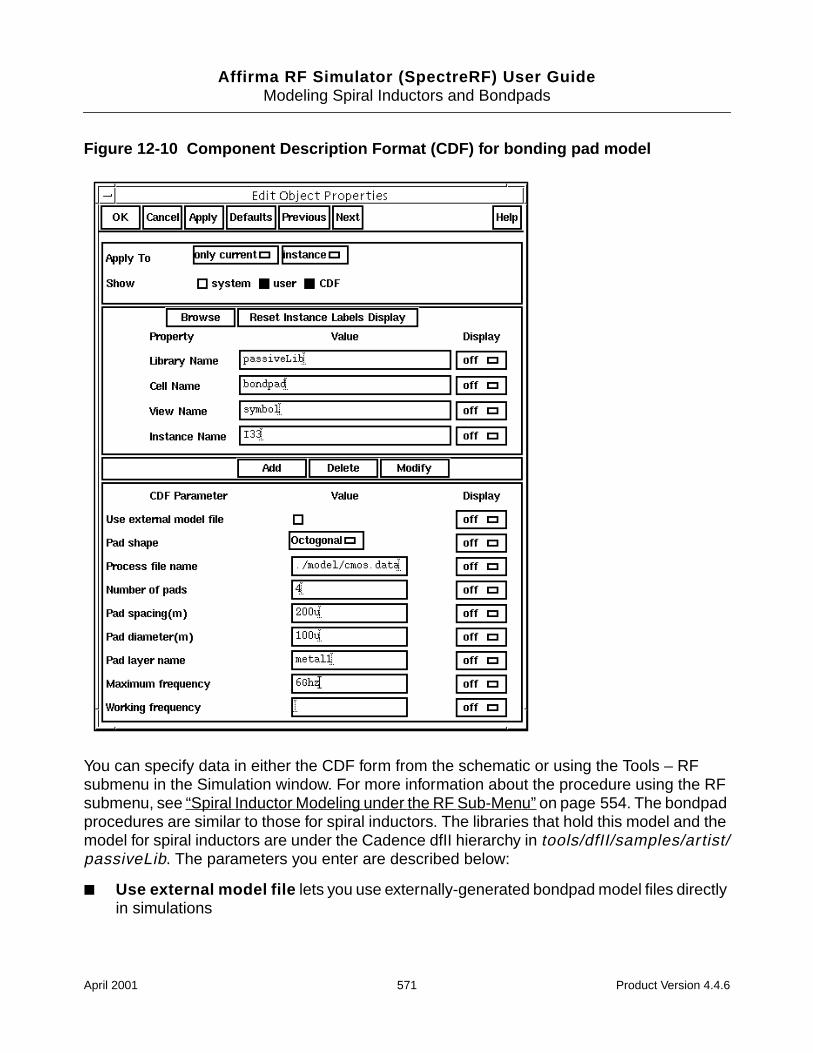
Affirma RF Simulator (SpectreRF) User GuideModeling Spiral Inductors and Bondpads
Figure 12-10 Component Description Format (CDF) for bonding pad model
You can specify data in either the CDF form from the schematic or using the Tools – RFsubmenu in the Simulation window. For more information about the procedure using the RFsubmenu, see “Spiral Inductor Modeling under the RF Sub-Menu” on page 554. The bondpadprocedures are similar to those for spiral inductors. The libraries that hold this model and themodel for spiral inductors are under the Cadence dfII hierarchy in tools/dfII/samples/artist/passiveLib. The parameters you enter are described below:
Use external model file lets you use externally-generated bondpad model files directlyin simulations
April 2001 571 Product Version 4.4.6
Affirma RF Simulator (SpectreRF) User GuideModeling Spiral Inductors and Bondpads
Process file name can be either an absolute file path or a relative path to the currentdirectory.
Pad shape can be square or octagonal. When this cyclic button is changed, the symbolshape changes accordingly.
Pad spacing is the distance between the centers of two adjacent pads. Remember thatthis is not the spacing between the adjacent edges.
Pad diameter is the diameter size of the single bonding pad. Remember that it is notthe size of the edges.
Pad layer name must have its corresponding layer name defined in the process file.
Number of pads lets you specify the number of pads.
Maximum Frequency and Working frequency – There are two types of modelsavailable: wide-band and narrow-band. When you specify the maximum frequency, awide-band model accurate up to the maximum frequency is generated. The defaultmaximum frequency is 10GHz.
When you supply the working frequency and also omit the maximum frequency, themodeler generates a narrow-band model that is accurate at the working frequency.
Modeling Issues
This section explains modeling issues related to the internal workings of the modeler and thegenerated models.
Wide-Band and Narrow-Band Models
Models are generated either as wide-band or narrow-band models. In most cases, you usethe wide-band model because it is more accurate for time-domain simulation.
The wide-band model is generated after fitting the charge-voltage relationships over afrequency range from DC to the maximum frequency. The model is created as a ROM(reduced order model) file. The netlisting code generates an nport, whose romdatfile is setto the ROM file to represent bonding-pads.
The narrow-band model only extracts the model exactly at the working frequency. An RCnetwork is derived from that extraction, and it is hoped that this model is accurate for areasonable frequency range around the working frequency. This RC network is alsorepresented internally as an nport.
April 2001 572 Product Version 4.4.6
Affirma RF Simulator (SpectreRF) User GuideModeling Spiral Inductors and Bondpads
Passivity Issues and Use of the Narrow-Band Model
The wide-band model is fitted to a sample of frequencies. For typical RF applications withoperating frequency of 1-2GHz, a maximum frequency of 10GHz covers sufficient frequencycontent and the model is generally very satisfactory. However, the fitting algorithm mightproduce an unstable model at frequencies higher than the maximum frequency. This is truebecause the model is extrapolating at these frequencies. This possible nonpassivity has noimpact on S-parameter small-signal analysis. It also does not harm simulation for most RFcircuits in transient and PSS analyses. It might, however, cause simulation to diverge when itis within a feedback loop of an unstable circuit, such as an oscillator.
You can use the narrow-band model if the wide-band model does not converge.Mathematically, the narrow-band model is an RC network that is guaranteed to be stable andpassive.
Noise Modeling
Currently, the bonding pad model does not model noise effects.
LNA Example
RF circuits operating at high frequencies are more susceptible to bonding pad effects. Usingthe process file in “Process File Preparation” on page 545, the series resistance of thebonding pad at 2GHz is about 450 Ohm and the series capacitance is 0.133p. These valuesare very similar to those in the literature[3].
This example shows the effects of the bonding pads in the following LNA circuit. Theoctagonal pad diameter is 100u and the spacing is 200u. It uses the process file described in“Process File Preparation” on page 545. A two-pad model is used, and the coupling effectsare included.
The example runs an S-parameter analysis without the bondpad and plots the results. Thebondpad is then added to the schematic, the simulation is rerun, and the results arecompared.
Setting Up and Running the S-Parameter Simulation
1. In the CIW, choose File – Open….
The Open File form appears.
2. In the Open File form, do the following and click OK:
April 2001 573 Product Version 4.4.6
Affirma RF Simulator (SpectreRF) User GuideModeling Spiral Inductors and Bondpads
a. Choose rfExamples for Library Name.
b. Highlight lna-pad for Cell Name.
c. Choose schematic for View Name.
The schematic appears
3. In the Schematic window, choose Tools – Analog Environment.
The Simulation window appears.
4. In the Simulation window, choose Setup – Model Libraries….
The Model Library Setup form appears.
5. In the Model Library Setup form, do the following:
a. In the Model Library File field, type the complete path to the npnStd.scs file
b. Click on Add.
April 2001 574 Product Version 4.4.6
Affirma RF Simulator (SpectreRF) User GuideModeling Spiral Inductors and Bondpads
The completed form looks like this;
c. Click OK.
6. In the Simulation window, choose Analyses – Choose….
The Choosing Analyses form appears.
7. In the Choosing Analyses form, do the following and then click OK:
a. Highlight sp for Analysis.
b. Highlight Frequency for Sweep Variable.
c. Highlight Start – Stop for Sweep Range.
d. Type 100M for Start and 5G for Stop.
e. Choose Linear for Sweep Type.
f. Highlight Number of Steps and type 50 in the adjacent field.
g. Highlight no for Do Noise.
April 2001 575 Product Version 4.4.6
Affirma RF Simulator (SpectreRF) User GuideModeling Spiral Inductors and Bondpads
The completed form looks like the this.
8. In the Simulation window, choose Simulation – Netlist and Run.
Be sure to check the CIW for a message that the simulation completed successfully.
Plotting the Results
1. In the Simulation window, choose Results – Direct Plot – S-Parameter….
The S-Parameter Results form appears.
2. In the S-Parameter Results form, do the following:
a. Highlight Replace for Plot Mode.
b. Highlight SP for Function.
c. Highlight Rectangular for Plot Type.
d. Highlight Magnitude for Modifier.
April 2001 576 Product Version 4.4.6
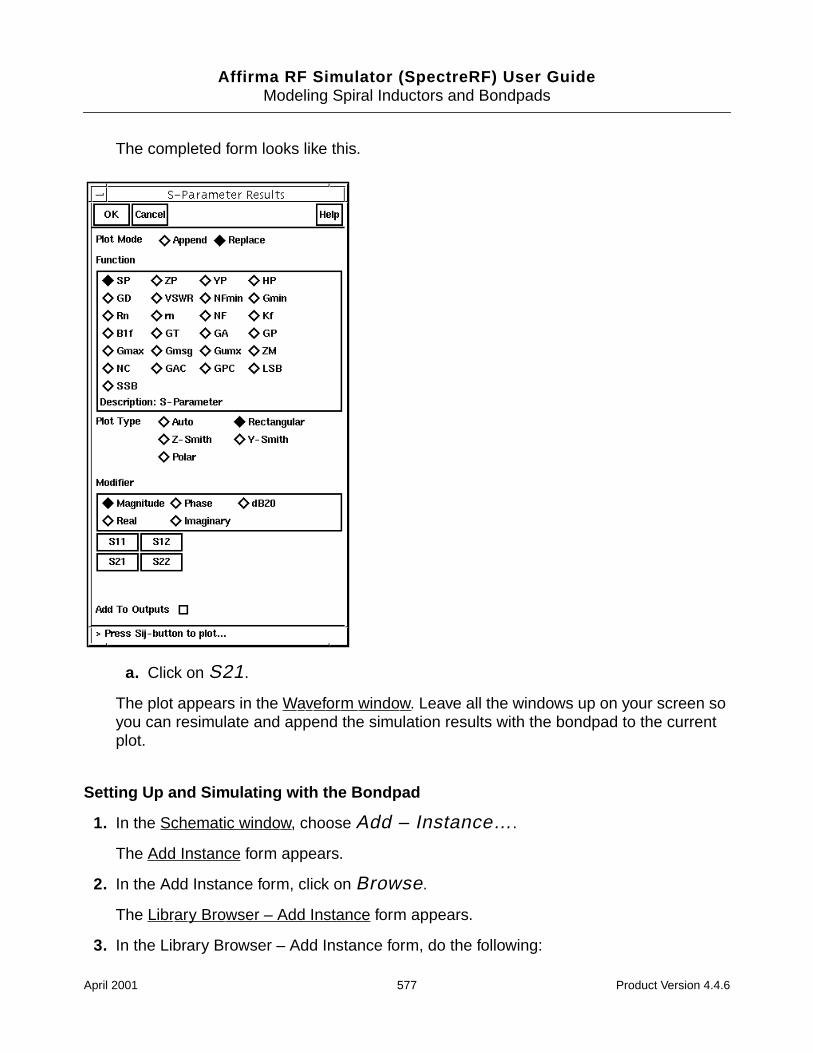
Affirma RF Simulator (SpectreRF) User GuideModeling Spiral Inductors and Bondpads
The completed form looks like this.
a. Click on S21.
The plot appears in the Waveform window. Leave all the windows up on your screen soyou can resimulate and append the simulation results with the bondpad to the currentplot.
Setting Up and Simulating with the Bondpad
1. In the Schematic window, choose Add – Instance….
The Add Instance form appears.
2. In the Add Instance form, click on Browse.
The Library Browser – Add Instance form appears.
3. In the Library Browser – Add Instance form, do the following:
April 2001 577 Product Version 4.4.6
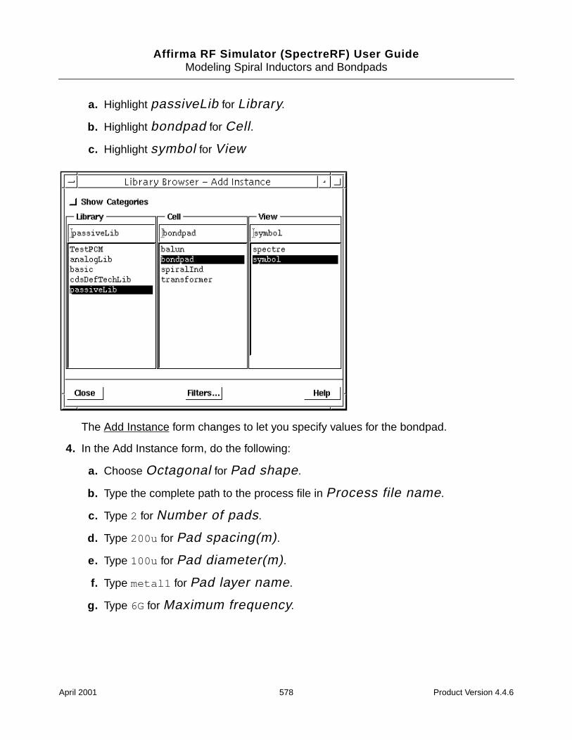
Affirma RF Simulator (SpectreRF) User GuideModeling Spiral Inductors and Bondpads
a. Highlight passiveLib for Library.
b. Highlight bondpad for Cell.
c. Highlight symbol for View
The Add Instance form changes to let you specify values for the bondpad.
4. In the Add Instance form, do the following:
a. Choose Octagonal for Pad shape.
b. Type the complete path to the process file in Process file name.
c. Type 2 for Number of pads.
d. Type 200u for Pad spacing(m).
e. Type 100u for Pad diameter(m).
f. Type metal1 for Pad layer name.
g. Type 6G for Maximum frequency.
April 2001 578 Product Version 4.4.6
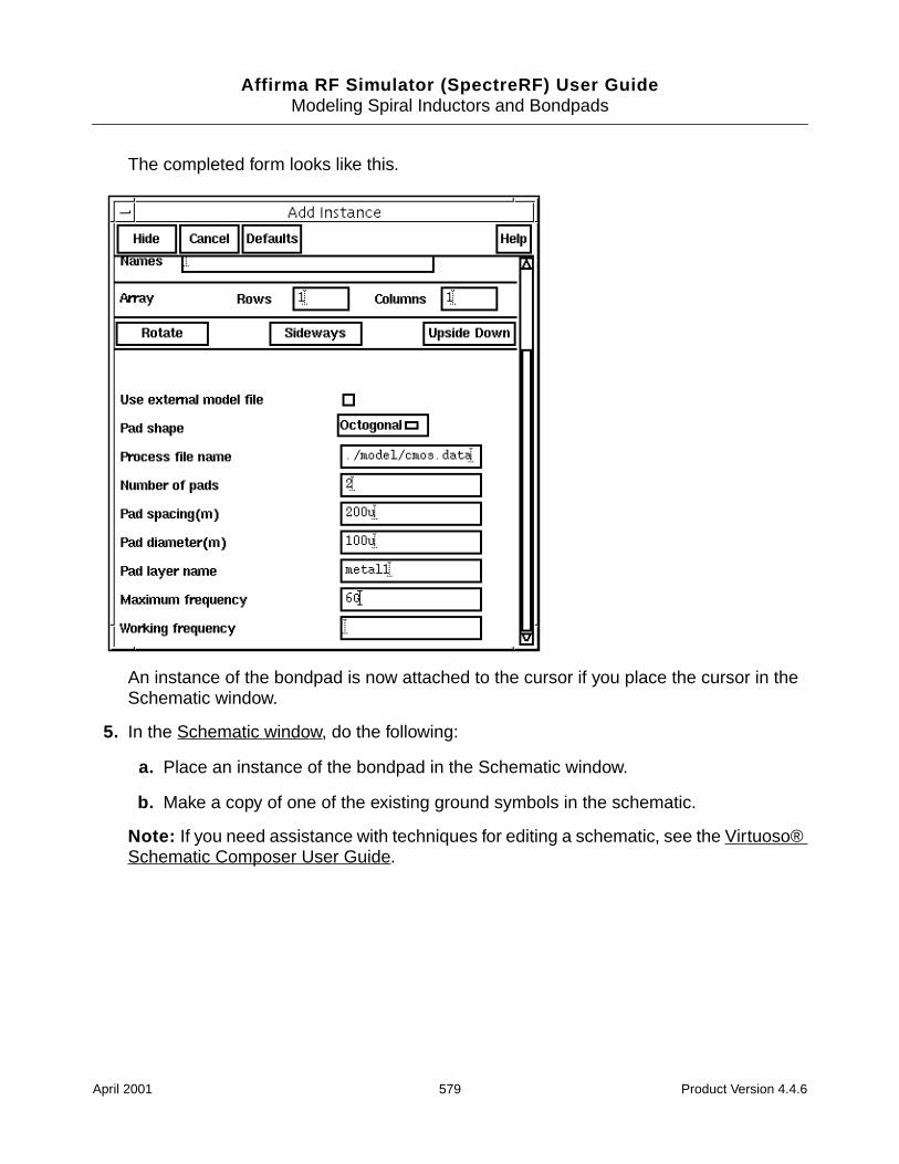
Affirma RF Simulator (SpectreRF) User GuideModeling Spiral Inductors and Bondpads
The completed form looks like this.
An instance of the bondpad is now attached to the cursor if you place the cursor in theSchematic window.
5. In the Schematic window, do the following:
a. Place an instance of the bondpad in the Schematic window.
b. Make a copy of one of the existing ground symbols in the schematic.
Note: If you need assistance with techniques for editing a schematic, see the Virtuoso®Schematic Composer User Guide.
April 2001 579 Product Version 4.4.6
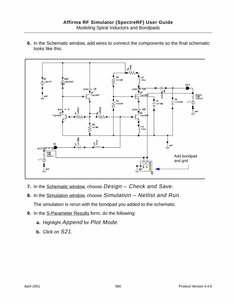
Affirma RF Simulator (SpectreRF) User GuideModeling Spiral Inductors and Bondpads
6. In the Schematic window, add wires to connect the components so the final schematiclooks like this.
7. In the Schematic window, choose Design – Check and Save.
8. In the Simulation window, choose Simulation – Netlist and Run.
The simulation is rerun with the bondpad you added to the schematic.
9. In the S-Parameter Results form, do the following:
a. Highlight Append for Plot Mode.
b. Click on S21.
Add bondpadand gnd
April 2001 580 Product Version 4.4.6
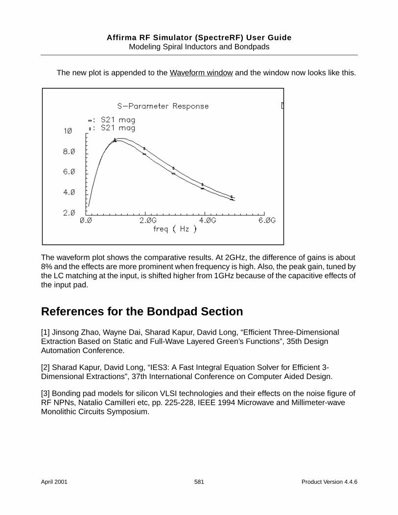
Affirma RF Simulator (SpectreRF) User GuideModeling Spiral Inductors and Bondpads
The new plot is appended to the Waveform window and the window now looks like this.
The waveform plot shows the comparative results. At 2GHz, the difference of gains is about8% and the effects are more prominent when frequency is high. Also, the peak gain, tuned bythe LC matching at the input, is shifted higher from 1GHz because of the capacitive effects ofthe input pad.
References for the Bondpad Section
[1] Jinsong Zhao, Wayne Dai, Sharad Kapur, David Long, “Efficient Three-DimensionalExtraction Based on Static and Full-Wave Layered Green’s Functions”, 35th DesignAutomation Conference.
[2] Sharad Kapur, David Long, “IES3: A Fast Integral Equation Solver for Efficient 3-Dimensional Extractions”, 37th International Conference on Computer Aided Design.
[3] Bonding pad models for silicon VLSI technologies and their effects on the noise figure ofRF NPNs, Natalio Camilleri etc, pp. 225-228, IEEE 1994 Microwave and Millimeter-waveMonolithic Circuits Symposium.
April 2001 581 Product Version 4.4.6
Affirma RF Simulator (SpectreRF) User Guide
13Behavioral Models and Methods for TopDown Design
The models and methods described in this document are for designing an analog RFsubsystem that fits into a larger DSP system. In particular, this document describes a newlibrary for Analog Artist. The library is a canonical set of top-down behavioral basebandmodels for exploring RF architectures in Analog Artist. The models have passband views formapping DSP measurements into RF measurements.
This library addresses the needs of RF designers who require a faster way to map systemspecifications into detailed designs. The baseband models facilitate fast evaluations ofcandidate RF architectures with respect to DSP metrics. The passband views of the modelsprovide a behavioral system testbench for checking detailed designs of individual systemcomponents.
Baseband models are behavioral models and all behavioral models sacrifice some accuracyfor lots of speed. Such sacrifices are usually acceptable in architectural studies becausemany implementation-dependent details do not affect high level decisions. The modelingapproach taken in top-down design is to simulate only those effects that drive the decisionsat hand.
Baseband modeling in no way replaces passband modeling. Some effects missed byequivalent baseband models can affect high level decisions. However, the application ofbaseband models early and passband models later minimizes the number of slow simulationsneeded at the lower levels of design abstraction; Baseband models quickly weed out designsthat would surely fail tests simulated with passband models.
The success of a modeling approach to top-down design hinges on knowing how the modelsfit into the design flow and knowing exactly what each modeling parameter means. Thischapter has two goals:
To describe the design flow from a modeling perspective
To define, as clearly and concisely as possible, the parameters that specify the models
April 2001 582 Product Version 4.4.6
Affirma RF Simulator (SpectreRF) User GuideBehavioral Models and Methods for Top Down Design
Top Down Design of RF Systems
Ideally, the digital signal processing, or DSP, team selects an RF subsystem that fits snuglyinto the DSP system. A snug fit means that the RF subsystem does exactly what it needs todo for the least general cost and it is described in full detail in a detailed design specificationthat describes how to build the RF subsystem.
Everything is known about a detailed design. It is the lowest level of abstraction. You canextract behavioral models of a detailed design from simulated measurements. The problemis that detailed designs usually do not exist until the project is complete. To jump directly to adetailed design implies that the design flow is bottom up. Bottom up flows are important inmany projects but not in all.
In a top down design flow, the DSP team writes a functional specification describing an RFsubsystem that has not yet been designed. The functional specification describes what theRF subsystem must do, as well as what it must not do. It does not describe how to build theRF subsystem.
The functional specification is the highest level of abstraction. Behavioral models created atthis level of abstraction are specified, not measured. At this point, the functional specificationmight be incomplete or inconsistent. A good top down design flow detects such problems asearly in the design cycle as possible because problems detected late in the design cycle canbe extremely costly to resolve.
DSP and RF engineers sometimes have trouble communicating through specificationsbecause the two groups deal with different metrics. For example, DSP engineers deal with biterror rates and error vector magnitude statistics whereas RF engineers deal withintercept points and noise figures.
The new models described here are designed to help RF system engineers in two ways.
First, the models enable the RF system designers quickly explore the RF architecturalspace, as specified by the DSP metrics, while letting the RF engineers specify the RFsystem components with RF metrics. The circuit implementations of the RF systemcomponents are easier to design and test when the components are specified withstandard RF metrics.
Second, the models can be switched quickly to a different view where the RF systemmodel can generate end-to-end RF metrics. With end-to-end metrics, the new view canquickly simulate how the detailed design of a particular RF system component affectsend-to-end performance.
Figure 13-1 on page 584 summarizes the top down design flow.
April 2001 583 Product Version 4.4.6
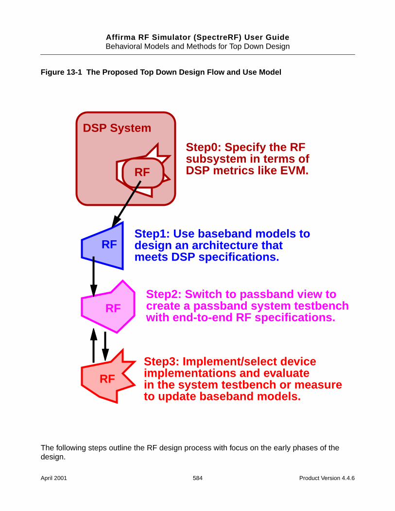
Affirma RF Simulator (SpectreRF) User GuideBehavioral Models and Methods for Top Down Design
Figure 13-1 The Proposed Top Down Design Flow and Use Model
The following steps outline the RF design process with focus on the early phases of thedesign.
RF
RF
DSP System
RF
RF
Step0: Specify the RFsubsystem in terms ofDSP metrics like EVM.
Step1: Use baseband models todesign an architecture thatmeets DSP specifications.
Step2: Switch to passband view tocreate a passband system testbench
Step3: Implement/select deviceimplementations and evaluatein the system testbench or measure
with end-to-end RF specifications.
to update baseband models.
April 2001 584 Product Version 4.4.6
Affirma RF Simulator (SpectreRF) User GuideBehavioral Models and Methods for Top Down Design
Step 0: Specify the RF subsystem in terms of DSP metrics.
This is called step 0 because it comes before the RF subsystem design flow but it must becompleted. This step distinguishes the end of the DSP design flow from the beginning of theRF design flow.
Step 1: Explore Candidate Architectures with Baseband Models
The first step in top down RF design is to select a candidate architecture. An architecture isa set of interconnected RF function blocks that, taken together, describe how a receiver ortransmitter operates. The function blocks are specified in terms of standard RF metrics, forexample, IP3, gain, bandwidth, and noise figure.
The models you use early in the design cycle as you explore RF architectures must run fast.Each simulation spans hundreds of symbols and each symbol can easily span thousands ofRF carrier cycles. The space defined by all function block specifications in the architecture isfar too vast to explore with slow (maximum precision) models. Models for architecturalexplorations must quickly reduce the design space down to a size that can be explored withmore precision.
The most efficient models for architectural exploration suppress the RF (IF) carrier and arecalled baseband models. In contrast, the passband models introduced in Step 2 do notsuppress carriers.
You can use the Circuit Optimizer during the exploration step to help balance the functionblock specifications for a candidate architecture. For example, the Circuit Optimizer canminimize RMS EVM while ensuring other measurements stay within acceptable limits.
After you determine the nominal specifications for each function block within the architectureyou must put tolerances around them. In the analog world specifications withouttolerances are meaningless. The tolerance space is usually explored with some mix ofexperience, feasibility, various analyses, and outright arbitrary decisions.
The baseband models can test candidate tolerances as well as help to determine sometolerances analytically. One way to test a candidate set of tolerances is to run a Monte Carloanalysis on the metric of interest, like RMS EVM or signal-to-noise ratio (SNR). Anotherapproach is to use the Circuit Optimizer in reverse, as a de-optimizer, to determine worstcase performance. Yet another approach is to compute each tolerance separately from aparametric plot. If all but 2 or 3 tolerances remain to be found, a multidimensional parametricanalysis can map out the performance space for easy identification of the necessarytolerances.
April 2001 585 Product Version 4.4.6
Affirma RF Simulator (SpectreRF) User GuideBehavioral Models and Methods for Top Down Design
Step 2: Switch to Passband Models and Create an RF System Testbench
The second step is to create a passband view of the system model. The passband view bothconfirms that the filters perform as expected and also creates an end-to-end testbench thatyou can use to design the individual function blocks. For computational efficiency, at any onetime only one or two selected function blocks are modeled at the device level for systempassband testing. All other blocks in the system are modeled behaviorally but with passbandmodels.
It is not practical to use the passband view to assess DSP metrics because Spectre analysiswould take too long. You also cannot use SpectreRF to reduce run times because theinstrumentation blocks have internal state variables and SpectreRF does not allow statevariables inside behavioral models.
However, you can apply SpectreRF to the passband behavioral view to derive end-to-end RFspecifications if you do it before inserting any device-level models into the testbench. Youderive the tolerances by performing the same Monte Carlo analysis or Circuit Optimizeranalysis you used to test the function block tolerances in Step 1, but this time you replace theDSP metrics with end-to-end RF metrics. Once you know how far the end-to-end RF metricscan vary, you can insert a device-level model of a function block into the testbench to see howclose it drives the system toward violating a derived end-to-end RF specification.
Step 3: Implement the Function Blocks With Active and Passive Devices
The last step in the top down design process is to implement the function blocks with devicemodels. Since the function blocks are specified in terms of standard RF metrics, you caneasily measure the modeling parameters to make sure they fall within the specifiedtolerances. You can also insert the measured parameters back into the baseband model ofthe system to check the DSP metrics, or insert the device-level model directly into thepassband testbench to check the derived end-to-end RF specifications.
Baseband Modeling
Figure 13-2 on page 587 mathematically defines a baseband representation of a passbandsignal. The i and q signals are the real and imaginary parts of a complex signal that rides onthe two phases of an RF carrier.
April 2001 586 Product Version 4.4.6
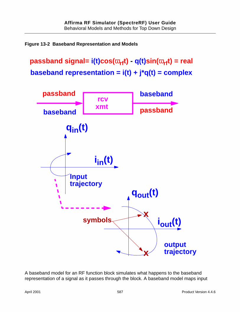
Affirma RF Simulator (SpectreRF) User GuideBehavioral Models and Methods for Top Down Design
Figure 13-2 Baseband Representation and Models
A baseband model for an RF function block simulates what happens to the basebandrepresentation of a signal as it passes through the block. A baseband model maps input
passband signal= i(t)cos( ωrf t) - q(t)sin( ωrf t) = real
passband basebandrcv
baseband xmt passband
baseband representation = i(t) + j*q(t) = complex
iin(t)
qin(t)
Inputtrajectory
iout (t)
qout (t)
outputtrajectory
x
x
symbols
April 2001 587 Product Version 4.4.6
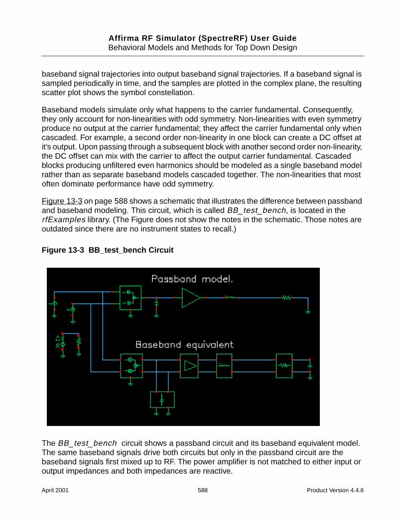
Affirma RF Simulator (SpectreRF) User GuideBehavioral Models and Methods for Top Down Design
baseband signal trajectories into output baseband signal trajectories. If a baseband signal issampled periodically in time, and the samples are plotted in the complex plane, the resultingscatter plot shows the symbol constellation.
Baseband models simulate only what happens to the carrier fundamental. Consequently,they only account for non-linearities with odd symmetry. Non-linearities with even symmetryproduce no output at the carrier fundamental; they affect the carrier fundamental only whencascaded. For example, a second order non-linearity in one block can create a DC offset atit’s output. Upon passing through a subsequent block with another second order non-linearity,the DC offset can mix with the carrier to affect the output carrier fundamental. Cascadedblocks producing unfiltered even harmonics should be modeled as a single baseband modelrather than as separate baseband models cascaded together. The non-linearities that mostoften dominate performance have odd symmetry.
Figure 13-3 on page 588 shows a schematic that illustrates the difference between passbandand baseband modeling. This circuit, which is called BB_test_bench, is located in therfExamples library. (The Figure does not show the notes in the schematic. Those notes areoutdated since there are no instrument states to recall.)
Figure 13-3 BB_test_bench Circuit
The BB_test_bench circuit shows a passband circuit and its baseband equivalent model.The same baseband signals drive both circuits but only in the passband circuit are thebaseband signals first mixed up to RF. The power amplifier is not matched to either input oroutput impedances and both impedances are reactive.
April 2001 588 Product Version 4.4.6
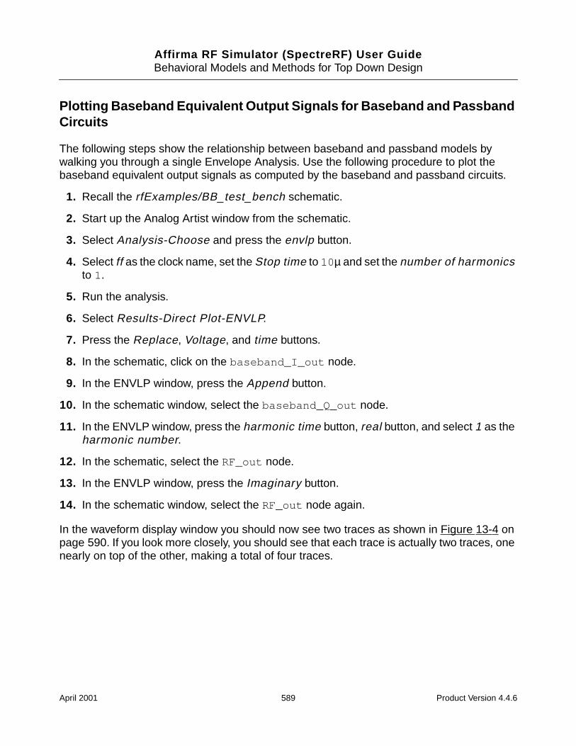
Affirma RF Simulator (SpectreRF) User GuideBehavioral Models and Methods for Top Down Design
Plotting Baseband Equivalent Output Signals for Baseband and PassbandCircuits
The following steps show the relationship between baseband and passband models bywalking you through a single Envelope Analysis. Use the following procedure to plot thebaseband equivalent output signals as computed by the baseband and passband circuits.
1. Recall the rfExamples/BB_test_bench schematic.
2. Start up the Analog Artist window from the schematic.
3. Select Analysis-Choose and press the envlp button.
4. Select ff as the clock name, set the Stop time to 10µ and set the number of harmonicsto 1.
5. Run the analysis.
6. Select Results-Direct Plot-ENVLP.
7. Press the Replace, Voltage, and time buttons.
8. In the schematic, click on the baseband_I_out node.
9. In the ENVLP window, press the Append button.
10. In the schematic window, select the baseband_Q_out node.
11. In the ENVLP window, press the harmonic time button, real button, and select 1 as theharmonic number.
12. In the schematic, select the RF_out node.
13. In the ENVLP window, press the Imaginary button.
14. In the schematic window, select the RF_out node again.
In the waveform display window you should now see two traces as shown in Figure 13-4 onpage 590. If you look more closely, you should see that each trace is actually two traces, onenearly on top of the other, making a total of four traces.
April 2001 589 Product Version 4.4.6
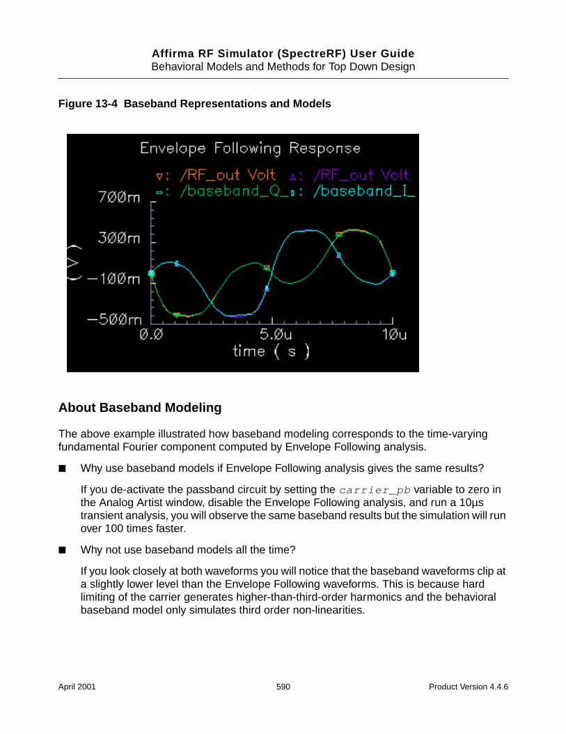
Affirma RF Simulator (SpectreRF) User GuideBehavioral Models and Methods for Top Down Design
Figure 13-4 Baseband Representations and Models
About Baseband Modeling
The above example illustrated how baseband modeling corresponds to the time-varyingfundamental Fourier component computed by Envelope Following analysis.
Why use baseband models if Envelope Following analysis gives the same results?
If you de-activate the passband circuit by setting the carrier_pb variable to zero inthe Analog Artist window, disable the Envelope Following analysis, and run a 10µstransient analysis, you will observe the same baseband results but the simulation will runover 100 times faster.
Why not use baseband models all the time?
If you look closely at both waveforms you will notice that the baseband waveforms clip ata slightly lower level than the Envelope Following waveforms. This is because hardlimiting of the carrier generates higher-than-third-order harmonics and the behavioralbaseband model only simulates third order non-linearities.
April 2001 590 Product Version 4.4.6
Affirma RF Simulator (SpectreRF) User GuideBehavioral Models and Methods for Top Down Design
Library Overview
The new library includes three kinds of models:
Instrumentation Models
Non-Linear Memoryless Models
Linear Models With Memory
The instrumentation models provide stimuli, diagnostics, and performance metrics relevant tothe DSP system.
Both the non-linear and linear models simulate the function blocks within an RF architectureand are specified in terms of common RF metrics. The function block models all include inputreferenced white Gaussian noise as specified by noise figure. Models are provided for thefollowing types of function blocks: amplifiers, mixers, filters1, and phase shifters.
The non-linear models simulate AM/AM conversion [1] with a third-order polynomial thatsaturates at the peak of the transfer curve. The polynomial is specified by the gain and eitherthe input-referred IP3 or output-referred 1 dB compression point. Only the baseband non-linear models simulate AM/PM conversion. AM/PM conversion [1] is an important effect thatis hard, if not impossible, to simulate with passband behavioral models.
Figure 13-5 on page 592 shows the basic baseband non-linearity.
1. Here, filters includes single resistors, capacitors, and inductors.
April 2001 591 Product Version 4.4.6
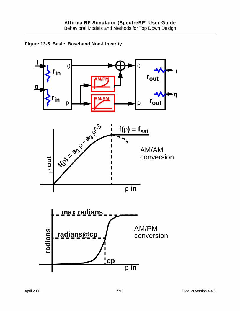
Affirma RF Simulator (SpectreRF) User GuideBehavioral Models and Methods for Top Down Design
Figure 13-5 Basic, Baseband Non-Linearity
i
q
θ
ρ
θ
ρ
i
q
AM/PM
AM/AMrin
rin rout
rout
f(ρ) = fsat
radi
ans
ρ in
max radians
radians@cp
cp
ρ ou
t
ρ in
f(ρ) =
a 1ρ - a
3ρ^
3
AM/AMconversion
AM/PMconversion
April 2001 592 Product Version 4.4.6
Affirma RF Simulator (SpectreRF) User GuideBehavioral Models and Methods for Top Down Design
The baseband models of reactive elements differentiate our approach from spreadsheet-based approaches to RF system design. The baseband capacitor and inductor models let yousimulate reactive loading effects in the time domain, where non-linearities are more naturallymodeled. In RF integrated circuits, loading effects are important because it is often hard tointegrate impedance matching networks.
The baseband models of reactive elements also play a key role in modeling filters. Most digitalcommunications text books [1,2] explain that you can model a passband transfer function atbaseband by simply frequency-shifting the transfer function. What these books do notdescribe is how to implement the resulting transfer function in a general circuit simulator suchas Spectre. The shifted transfer function usually lacks complex conjugate symmetry aboutzero frequency and therefore has a complex impulse response.
The first consequence of modeling RF function blocks at baseband is that all equivalentbaseband models have four terminals instead of two:
One set of terminals represents in-phase signals, i(t) in Figure 13-2 on page 587.
The other set of terminals represents quadrature signals, q(t) in Figure 13-2 onpage 587.
The mathematics below applies to capacitors as well as inductors1. In Figure 13-6 onpage 594, the ideas behind a time-varying coordinate transformation used to model reactiveelements at baseband are summarized.
1. The inductor baseband equivalent model derivation has a well-documented but little-known electro-mechanical analogy. The four inductor terminals resemble the stator wind-ings of a two-phase rotating machine with shaft speed equal to the RF carrier frequency.Modulation is mathematically analogous to the flux linking a stator winding due to cur-rents in orthogonal rotor windings. The flux depends on shaft angle just as a modulatedsignal depends on carrier phase. Transforming the vectorial equation for v=Ldi/dt to therotor reference frame suppresses the RF carrier and introduces a speed voltage[3,4,5,6,7,8,9], or back electro-motive force (back EMF), that couples the differentialequations.
April 2001 593 Product Version 4.4.6
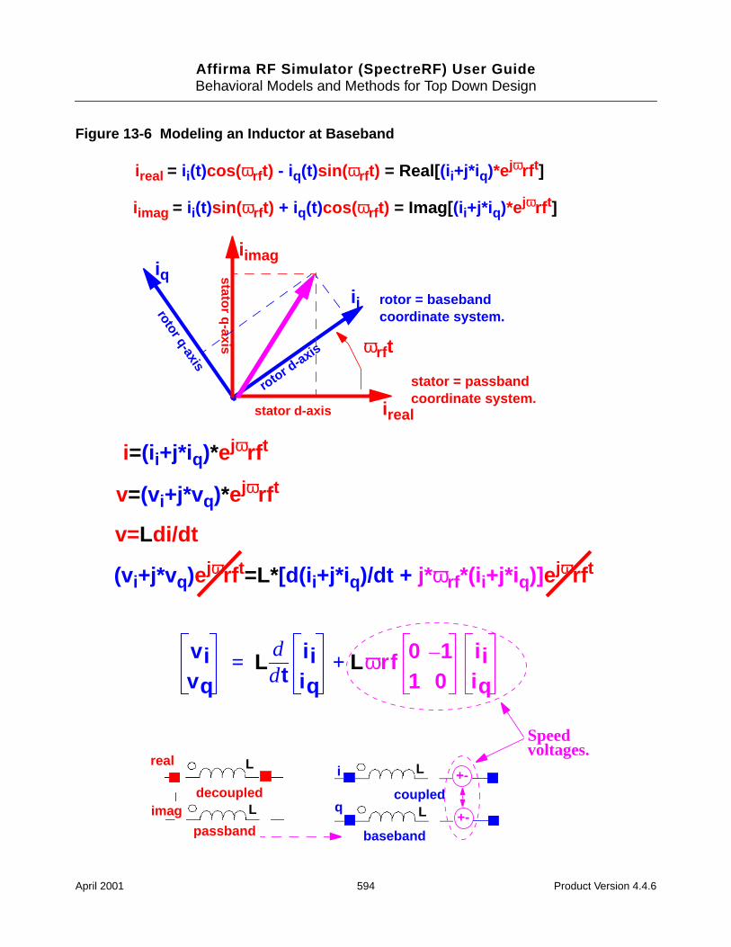
Affirma RF Simulator (SpectreRF) User GuideBehavioral Models and Methods for Top Down Design
Figure 13-6 Modeling an Inductor at Baseband
ireal = ii(t)cos( ωrf t) - iq(t)sin( ωrf t) = Real[ (ii+j*i q)*ejωrf t]
iimag = ii(t)sin( ωrf t) + iq(t)cos( ωrf t) = Imag[ (ii+j*i q)*ejωrf t]
rotor = baseband
stator = passband
coordinate system.
coordinate system.
ωrf t
ireal
iimag
ii
iq
stator d-axis
stator q-axis
rotor d-axis
rotor q-axis
i=(ii+j*i q)*ejωrf t
v=(vi+j*vq)*ejωrf t
v=Ldi/dt
(vi+j*vq)ejωrf t=L*[d(i i+j*i q)/dt + j*ωrf*(ii+j*i q)]ejωrf t
v ivq
Ltd
d i iiq
Lωrf 0 1–
1 0i iiq
+=
real
imagdecoupled
baseband
coupled
i
q
+-
+-
L
L
L
L
Speedvoltages.
passband
April 2001 594 Product Version 4.4.6
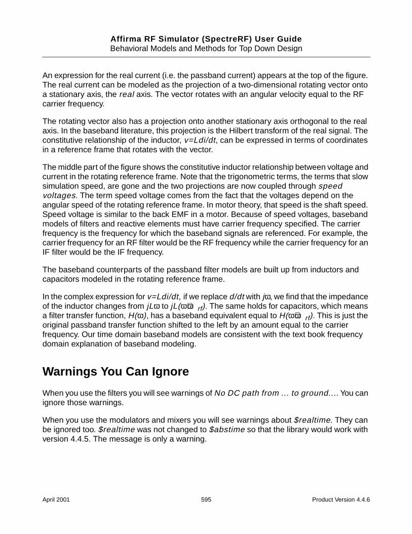
Affirma RF Simulator (SpectreRF) User GuideBehavioral Models and Methods for Top Down Design
An expression for the real current (i.e. the passband current) appears at the top of the figure.The real current can be modeled as the projection of a two-dimensional rotating vector ontoa stationary axis, the real axis. The vector rotates with an angular velocity equal to the RFcarrier frequency.
The rotating vector also has a projection onto another stationary axis orthogonal to the realaxis. In the baseband literature, this projection is the Hilbert transform of the real signal. Theconstitutive relationship of the inductor, v=Ldi/dt, can be expressed in terms of coordinatesin a reference frame that rotates with the vector.
The middle part of the figure shows the constitutive inductor relationship between voltage andcurrent in the rotating reference frame. Note that the trigonometric terms, the terms that slowsimulation speed, are gone and the two projections are now coupled through speedvoltages. The term speed voltage comes from the fact that the voltages depend on theangular speed of the rotating reference frame. In motor theory, that speed is the shaft speed.Speed voltage is similar to the back EMF in a motor. Because of speed voltages, basebandmodels of filters and reactive elements must have carrier frequency specified. The carrierfrequency is the frequency for which the baseband signals are referenced. For example, thecarrier frequency for an RF filter would be the RF frequency while the carrier frequency for anIF filter would be the IF frequency.
The baseband counterparts of the passband filter models are built up from inductors andcapacitors modeled in the rotating reference frame.
In the complex expression for v=Ldi/dt, if we replace d/dt with jω, we find that the impedanceof the inductor changes from jLω to jL(ω+ωrf). The same holds for capacitors, which meansa filter transfer function, H(ω), has a baseband equivalent equal to H(ω+ωrf). This is just theoriginal passband transfer function shifted to the left by an amount equal to the carrierfrequency. Our time domain baseband models are consistent with the text book frequencydomain explanation of baseband modeling.
Warnings You Can Ignore
When you use the filters you will see warnings of No DC path from ... to ground.... You canignore those warnings.
When you use the modulators and mixers you will see warnings about $realtime. They canbe ignored too. $realtime was not changed to $abstime so that the library would work withversion 4.4.5. The message is only a warning.
April 2001 595 Product Version 4.4.6

Affirma RF Simulator (SpectreRF) User GuideBehavioral Models and Methods for Top Down Design
Use Model and Design Example
This section focuses on the baseband models and their use during the architectural designphase. The following steps walk you through
The construction of a baseband model for a receiver
The application of the Circuit Optimizer to help balance specifications among thefunction blocks
The process of creating a passband testbench
The design goals were chosen arbitrarily. The example is meant simply to illustrate how touse the library. The example is a derivative of the design found in [10]. If in the steps below,some model parameters are not specified, leave them as default values.
The receiver is constructed from left to right, from input to output. Except for resistorsand ports, all models come from the rfLib. Unless otherwise instructed, leave the portresistances at their default values of 50 Ohms.
1. Bring up a blank Composer schematic.
2. From the measurement category in the rfLib, instantiate a CDMA_reverse_xmitblock. This model is a CDMA signal source. Connect a resistor between thei_bin_node and the q_bin_node . We will not need those outputs and do not want tobe bothered with warnings about unused pins.
3. From the measurement category, instantiate a BB_driver to the right of the last blockwith its input pins aligned with the two top pins of the CDMA source. Wire thei_out_node pin of the source to the I_in pin of the BB_driver. Wire the q_out_nodepin of the source to the Q_in pin of the BB_driver. Set the dBm-out@1v peak inparameter of the BB_driver to -16 . The driver will convert 1 peak volt from the signalsource to -16 dBm referenced to the output resistance of the driver.
4. To the right of the driver, instantiate a low noise amplifier, LNA_BB from the top_dwnBBcategory, align and wire the pins straight across, then set parameters as shown inFigure 13-7 on page 597.
April 2001 596 Product Version 4.4.6
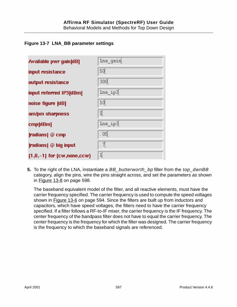
Affirma RF Simulator (SpectreRF) User GuideBehavioral Models and Methods for Top Down Design
Figure 13-7 LNA_BB parameter settings
5. To the right of the LNA, instantiate a BB_butterworth_bp filter from the top_dwnBBcategory, align the pins, wire the pins straight across, and set the parameters as shownin Figure 13-8 on page 598.
The baseband equivalent model of the filter, and all reactive elements, must have thecarrier frequency specified. The carrier frequency is used to compute the speed voltagesshown in Figure 13-6 on page 594. Since the filters are built up from inductors andcapacitors, which have speed voltages, the filters need to have the carrier frequencyspecified. If a filter follows a RF-to-IF mixer, the carrier frequency is the IF frequency. Thecenter frequency of the bandpass filter does not have to equal the carrier frequency. Thecenter frequency is the frequency for which the filter was designed. The carrier frequencyis the frequency to which the baseband signals are referenced.
April 2001 597 Product Version 4.4.6
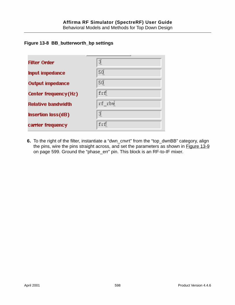
Affirma RF Simulator (SpectreRF) User GuideBehavioral Models and Methods for Top Down Design
Figure 13-8 BB_butterworth_bp settings
6. To the right of the filter, instantiate a “dwn_cnvrt” from the “top_dwnBB” category, alignthe pins, wire the pins straight across, and set the parameters as shown in Figure 13-9on page 599. Ground the “phase_err” pin. This block is an RF-to-IF mixer.
April 2001 598 Product Version 4.4.6
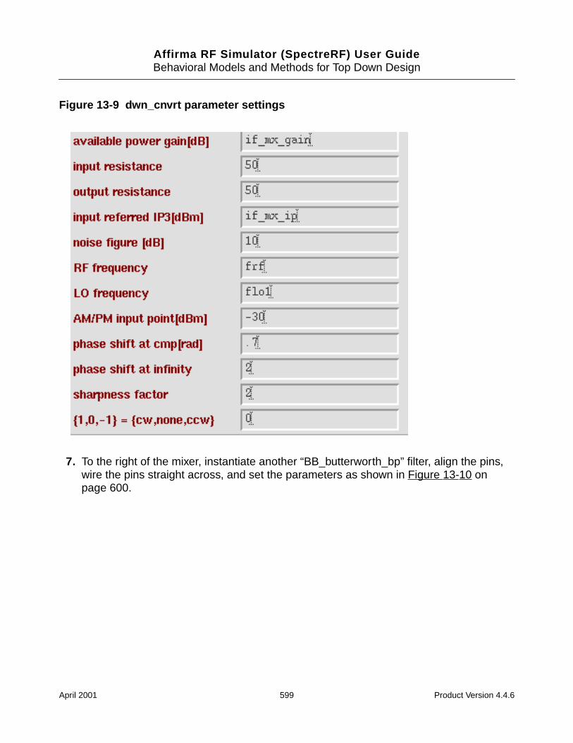
Affirma RF Simulator (SpectreRF) User GuideBehavioral Models and Methods for Top Down Design
Figure 13-9 dwn_cnvrt parameter settings
7. To the right of the mixer, instantiate another “BB_butterworth_bp” filter, align the pins,wire the pins straight across, and set the parameters as shown in Figure 13-10 onpage 600.
April 2001 599 Product Version 4.4.6
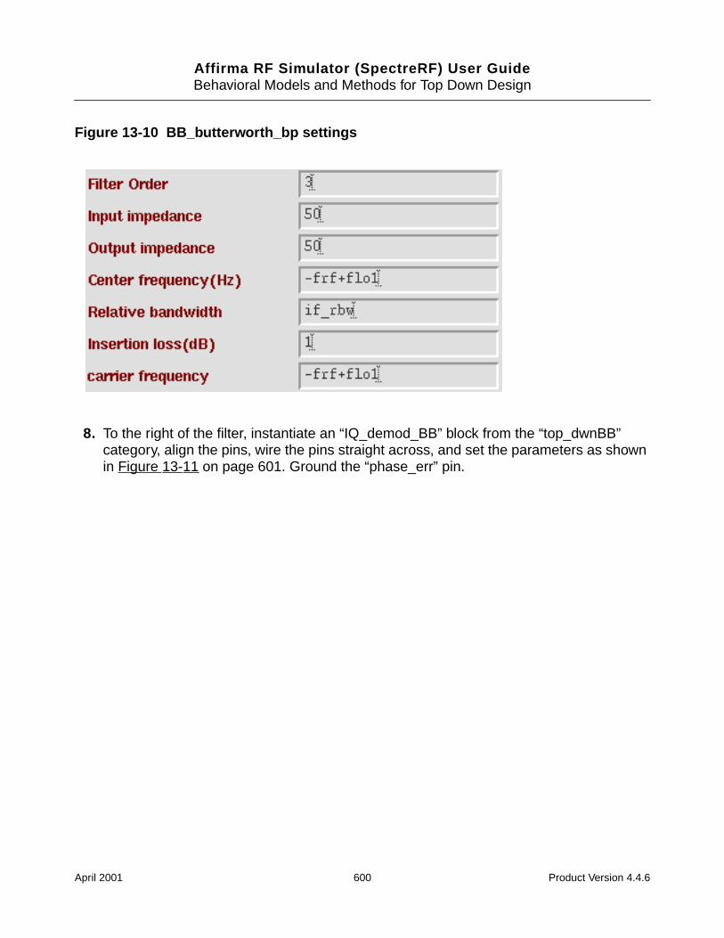
Affirma RF Simulator (SpectreRF) User GuideBehavioral Models and Methods for Top Down Design
Figure 13-10 BB_butterworth_bp settings
8. To the right of the filter, instantiate an “IQ_demod_BB” block from the “top_dwnBB”category, align the pins, wire the pins straight across, and set the parameters as shownin Figure 13-11 on page 601. Ground the “phase_err” pin.
April 2001 600 Product Version 4.4.6
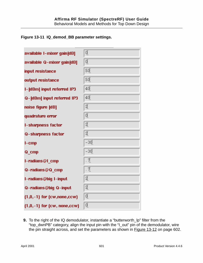
Affirma RF Simulator (SpectreRF) User GuideBehavioral Models and Methods for Top Down Design
Figure 13-11 IQ_demod_BB parameter settings.
9. To the right of the IQ demodulator, instantiate a “butterworth_lp” filter from the“top_dwnPB” category, align the input pin with the “I_out” pin of the demodulator, wirethe pin straight across, and set the parameters as shown in Figure 13-12 on page 602.
April 2001 601 Product Version 4.4.6
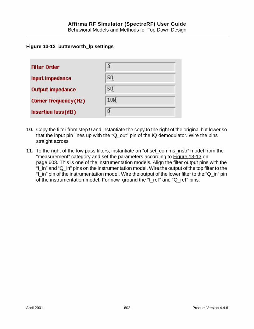
Affirma RF Simulator (SpectreRF) User GuideBehavioral Models and Methods for Top Down Design
Figure 13-12 butterworth_lp settings
10. Copy the filter from step 9 and instantiate the copy to the right of the original but lower sothat the input pin lines up with the “Q_out” pin of the IQ demodulator. Wire the pinsstraight across.
11. To the right of the low pass filters, instantiate an “offset_comms_instr” model from the“measurement” category and set the parameters according to Figure 13-13 onpage 603. This is one of the instrumentation models. Align the filter output pins with the“I_in” and “Q_in” pins on the instrumentation model. Wire the output of the top filter to the“I_in” pin of the instrumentation model. Wire the output of the lower filter to the “Q_in” pinof the instrumentation model. For now, ground the “I_ref” and “Q_ref” pins.
April 2001 602 Product Version 4.4.6
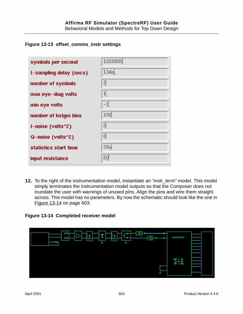
Affirma RF Simulator (SpectreRF) User GuideBehavioral Models and Methods for Top Down Design
Figure 13-13 offset_comms_instr settings
12. To the right of the instrumentation model, instantiate an “instr_term” model. This modelsimply terminates the instrumentation model outputs so that the Composer does notinundate the user with warnings of unused pins. Align the pins and wire them straightacross. This model has no parameters. By now the schematic should look like the one inFigure 13-14 on page 603.
Figure 13-14 Completed receiver model
April 2001 603 Product Version 4.4.6
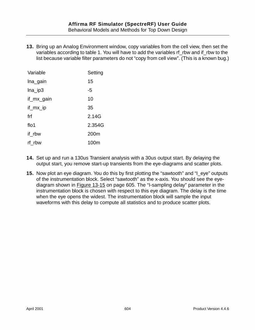
Affirma RF Simulator (SpectreRF) User GuideBehavioral Models and Methods for Top Down Design
13. Bring up an Analog Environment window, copy variables from the cell view, then set thevariables according to table 1. You will have to add the variables rf_rbw and if_rbw to thelist because variable filter parameters do not “copy from cell view”. (This is a known bug.)
14. Set up and run a 130us Transient analysis with a 30us output start. By delaying theoutput start, you remove start-up transients from the eye-diagrams and scatter plots.
15. Now plot an eye diagram. You do this by first plotting the “sawtooth” and “I_eye” outputsof the instrumentation block. Select “sawtooth” as the x-axis. You should see the eye-diagram shown in Figure 13-15 on page 605. The “I-sampling delay” parameter in theinstrumentation block is chosen with respect to this eye diagram. The delay is the timewhen the eye opens the widest. The instrumentation block will sample the inputwaveforms with this delay to compute all statistics and to produce scatter plots.
Variable Setting
lna_gain 15
lna_ip3 -5
if_mx_gain 10
if_mx_ip 35
frf 2.14G
flo1 2.354G
if_rbw 200m
rf_rbw 100m
April 2001 604 Product Version 4.4.6
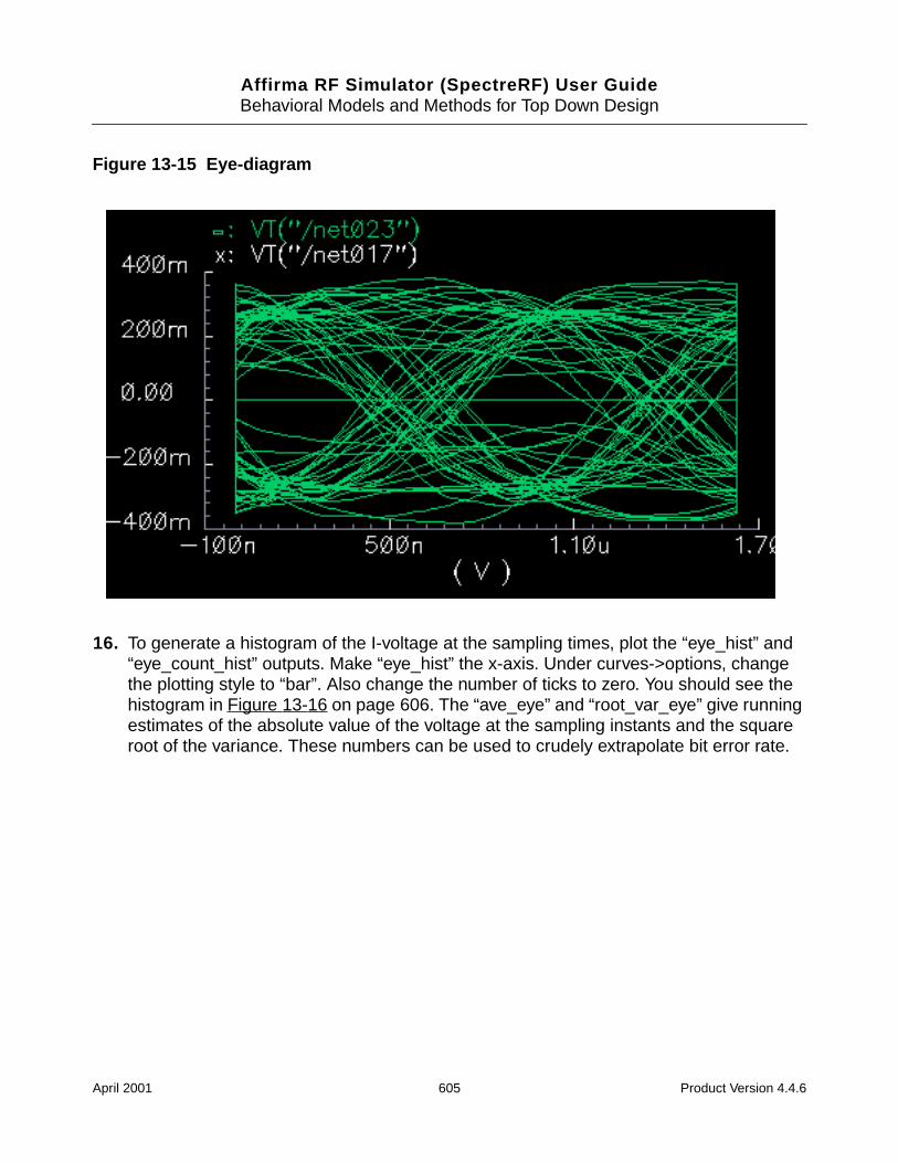
Affirma RF Simulator (SpectreRF) User GuideBehavioral Models and Methods for Top Down Design
Figure 13-15 Eye-diagram
16. To generate a histogram of the I-voltage at the sampling times, plot the “eye_hist” and“eye_count_hist” outputs. Make “eye_hist” the x-axis. Under curves->options, changethe plotting style to “bar”. Also change the number of ticks to zero. You should see thehistogram in Figure 13-16 on page 606. The “ave_eye” and “root_var_eye” give runningestimates of the absolute value of the voltage at the sampling instants and the squareroot of the variance. These numbers can be used to crudely extrapolate bit error rate.
April 2001 605 Product Version 4.4.6
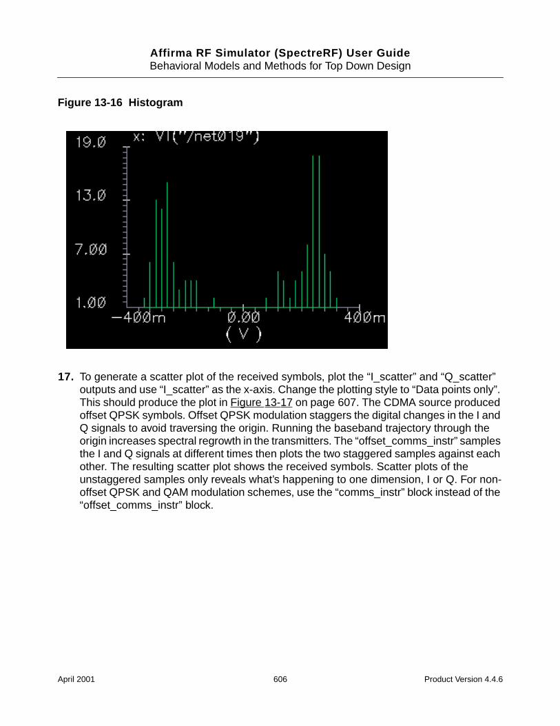
Affirma RF Simulator (SpectreRF) User GuideBehavioral Models and Methods for Top Down Design
Figure 13-16 Histogram
17. To generate a scatter plot of the received symbols, plot the “I_scatter” and “Q_scatter”outputs and use “I_scatter” as the x-axis. Change the plotting style to “Data points only”.This should produce the plot in Figure 13-17 on page 607. The CDMA source producedoffset QPSK symbols. Offset QPSK modulation staggers the digital changes in the I andQ signals to avoid traversing the origin. Running the baseband trajectory through theorigin increases spectral regrowth in the transmitters. The “offset_comms_instr” samplesthe I and Q signals at different times then plots the two staggered samples against eachother. The resulting scatter plot shows the received symbols. Scatter plots of theunstaggered samples only reveals what’s happening to one dimension, I or Q. For non-offset QPSK and QAM modulation schemes, use the “comms_instr” block instead of the“offset_comms_instr” block.
April 2001 606 Product Version 4.4.6
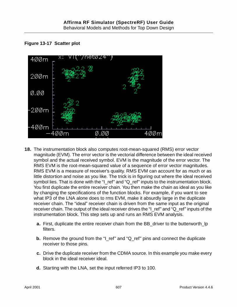
Affirma RF Simulator (SpectreRF) User GuideBehavioral Models and Methods for Top Down Design
Figure 13-17 Scatter plot
18. The instrumentation block also computes root-mean-squared (RMS) error vectormagnitude (EVM). The error vector is the vectorial difference between the ideal receivedsymbol and the actual received symbol. EVM is the magnitude of the error vector. TheRMS EVM is the root-mean-squared value of a sequence of error vector magnitudes.RMS EVM is a measure of receiver’s quality. RMS EVM can account for as much or aslittle distortion and noise as you like. The trick is in figuring out where the ideal receivedsymbol lies. That is done with the “I_ref” and “Q_ref” inputs to the instrumentation block.You first duplicate the entire receiver chain. You then make the chain as ideal as you likeby changing the specifications of the function blocks. For example, if you want to seewhat IP3 of the LNA alone does to rms EVM, make it absurdly large in the duplicatereceiver chain. The “ideal” receiver chain is driven from the same input as the originalreceiver chain. The output of the ideal receiver drives the “I_ref” and “Q_ref” inputs of theinstrumentation block. This step sets up and runs an RMS EVM analysis.
a. First, duplicate the entire receiver chain from the BB_driver to the butterworth_lpfilters.
b. Remove the ground from the “I_ref” and “Q_ref” pins and connect the duplicatereceiver to those pins.
c. Drive the duplicate receiver from the CDMA source. In this example you make everyblock in the ideal receiver ideal.
d. Starting with the LNA, set the input referred IP3 to 100.
April 2001 607 Product Version 4.4.6
Affirma RF Simulator (SpectreRF) User GuideBehavioral Models and Methods for Top Down Design
e. Set the “1,0,-1....” parameter at the end of the properties form to 0. This eliminatesAM/PM conversion.
f. Bring up the edit properties form for the RF bandpass filter. Change the cell nameto “BB_loss”. The reference impedance should equal the output resistance of thefilter and you should not have change it. The sole purpose of the BB_loss model isto replace a filter for an RMS EVM analysis. The BB_loss model retains the filter’sloss but eliminates the dynamics so you can see what, if any, affect the filter has onEVM through intersymbol interference. You can replace the filter with straight wiresif you want to eliminate the loss too but this example does not do that.
g. Change the RF-to-IF mixer IP3 to 100.
h. Bring up the edit properties form for the IF filter and change the cell name toBB_loss.
i. Change the demodulator IP3 parameters to 100.
j. Replace the low pass filters with wires.
k. Check and save the circuit then re-run the analysis.
l. Plot the RMS_EVM output of the instrumentation block. The trace starts at 30us,which is the “statistics start time” parameter of the block. This parameter allows youto keep start-up transients out of the statistics. The trace settles out at 25.84 Volts.That means that after 130us of data, and ignoring the first 30us, the RMS EVM is25.84%. The EVM measurement is normalized to the RMS magnitude of the idealsymbol then multiplied by 100 to express the measurement as a percentage.
19. There is one more construction step before proceeding to the Circuit Optimizerapplication. The Circuit Optimizer will be set up to minimize rms noise subject toperformance constraints. This step replicates the receiver model yet one more time togenerate the noise measurement.
a. Copy the original receiver chain from the BB_driver up to and including the low passfilters and place the copy above the original receiver model.
b. Ground the “Q_in” pin on the BB_driver and drive the “I_in” pin with a 50mV DCvoltage source.
c. Load the low pass filters with a res_BB model from the top_dwnBB category. Usethe default parameters and ground the output pins.
d. Check and save the schematic.
e. Set up a Noise analysis from 0 to 100MHz. In the noise form, set the Output Noiseto “voltage”, select the “I_in” pin on the res_BB model as the Positive Output Node
April 2001 608 Product Version 4.4.6
Affirma RF Simulator (SpectreRF) User GuideBehavioral Models and Methods for Top Down Design
and the “I_out” pin as the Negative Output Node. Select the input DC voltage sourceas the Input Noise.
f. Run both the Noise and the Transient analyses to make sure everything works.
g. Bring up a Waveform Calculator and under Special Functions, click on “rmsNoise”.In the form that comes up enter From 0 To 100M.
h. Bring up the Circuit Optimizer and click on “Goals” then “Add...”.
i. Click on “Get Expression”, which is to the right of the Calculator label. Type in “rmsnoise” in the “Name” field. For Target, enter 0.1u. For Acceptable, enter 20u. ClickOK. By default, the Circuit Optimizer will minimize a goal.
j. In the Waveform Calculator, click on “vt” then click on the rms_EVM output of theinstrumentation block in the schematic.
k. In the Waveform Calculator, click on Special Functions then click on “Value...”.Interpolate at the last time point, 130us.
l. In the Circuit Optimizer window, add another goal. Again, in the Calculator line, click“Get Expression”. Name this expression “evm”, set the Direction to <=, set the targetto 25, enter 10 for Acceptable then click the “% within Target” button. Click OK.
m. In the Waveform Calculator, click on vt again then click on the I_in pin of theinstrumentation block.
n. In the Waveform Calculator, click on Special Functions then click on “rms”. We willtry to keep the rms value of this signal level above 300mV. Note that all goals mustbe scalars.
o. In the Circuit Optimizer window add another goal, name it sig_level, set the directionto >=, the target to 300m, and set Acceptable to 10%.
p. Add the variables such that the Optimizer window looks like Figure 13-18 onpage 610.
q. Set the number of runs to 12 and start the Circuit Optimizer analysis. This will takea several hours to complete.
April 2001 609 Product Version 4.4.6
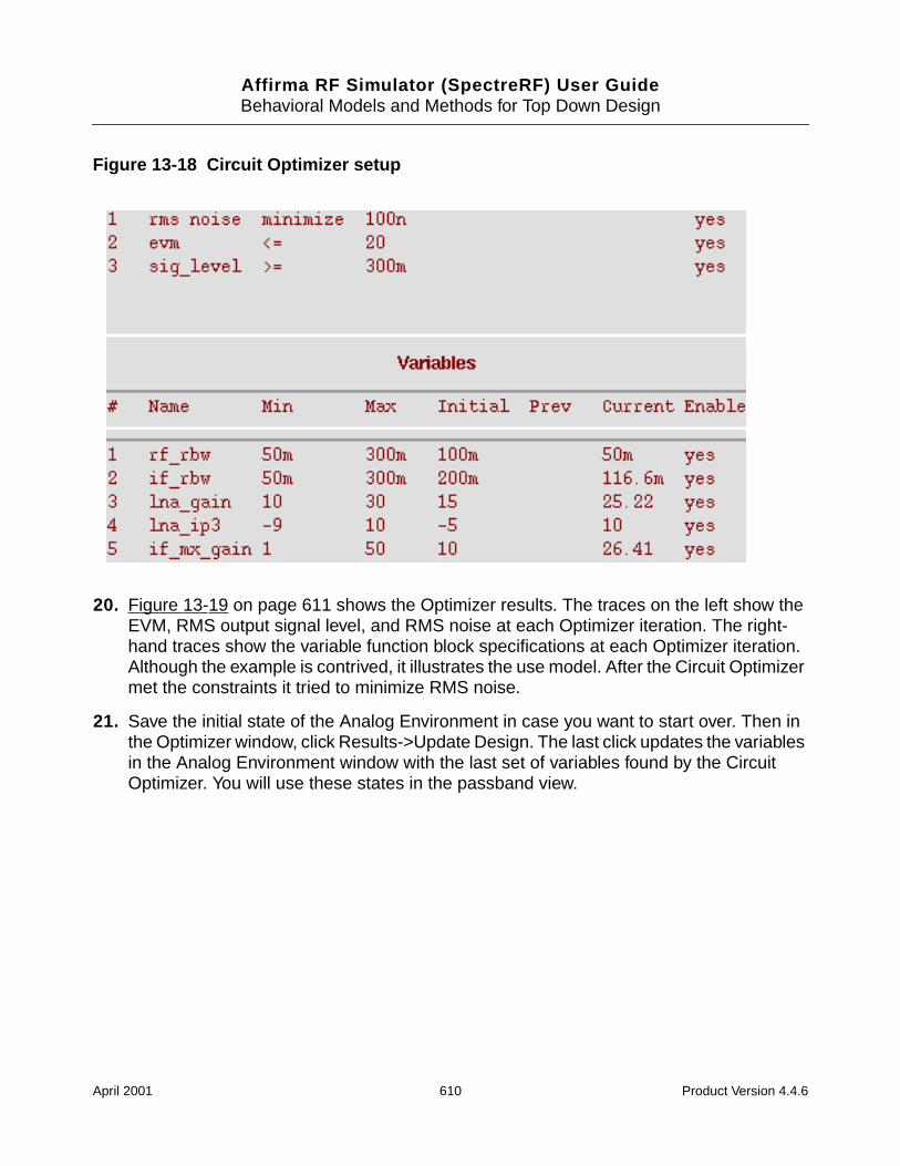
Affirma RF Simulator (SpectreRF) User GuideBehavioral Models and Methods for Top Down Design
Figure 13-18 Circuit Optimizer setup
20. Figure 13-19 on page 611 shows the Optimizer results. The traces on the left show theEVM, RMS output signal level, and RMS noise at each Optimizer iteration. The right-hand traces show the variable function block specifications at each Optimizer iteration.Although the example is contrived, it illustrates the use model. After the Circuit Optimizermet the constraints it tried to minimize RMS noise.
21. Save the initial state of the Analog Environment in case you want to start over. Then inthe Optimizer window, click Results->Update Design. The last click updates the variablesin the Analog Environment window with the last set of variables found by the CircuitOptimizer. You will use these states in the passband view.
April 2001 610 Product Version 4.4.6
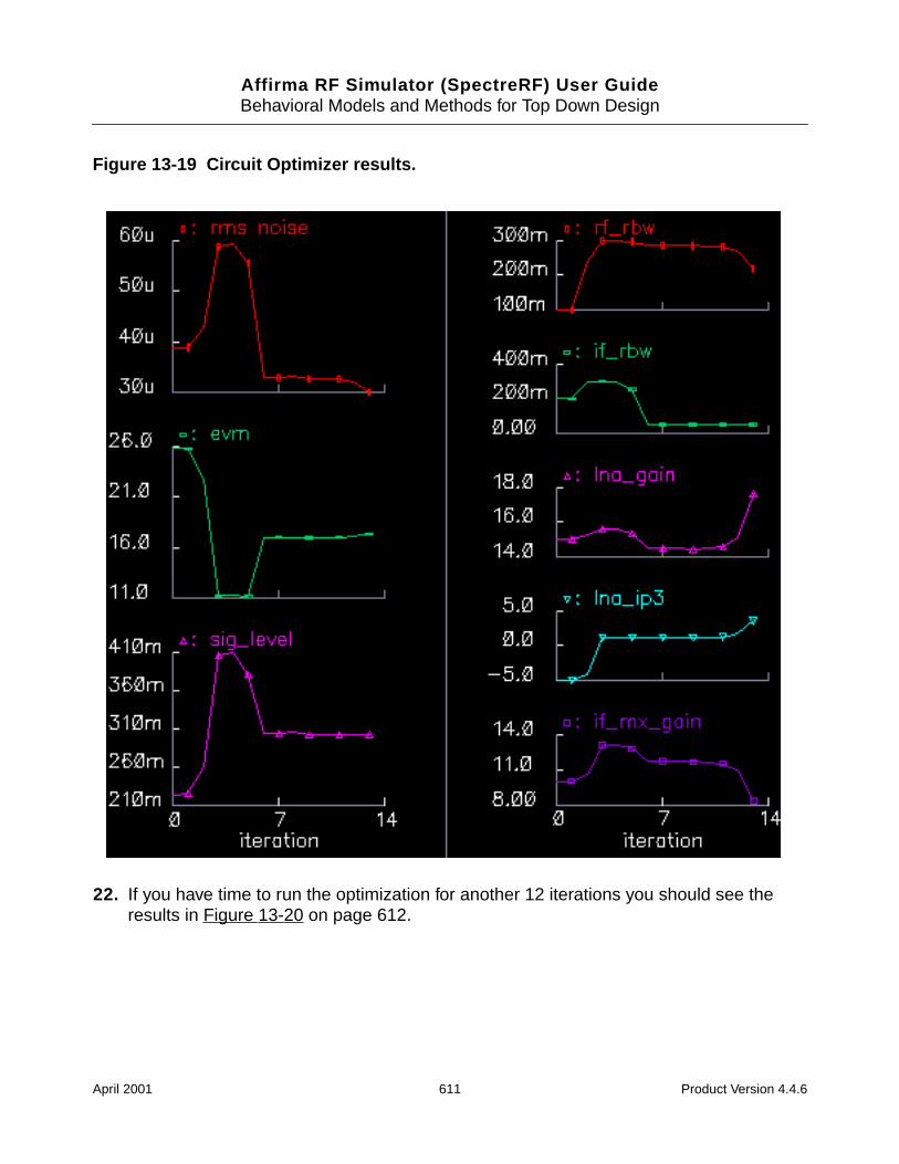
Affirma RF Simulator (SpectreRF) User GuideBehavioral Models and Methods for Top Down Design
Figure 13-19 Circuit Optimizer results.
22. If you have time to run the optimization for another 12 iterations you should see theresults in Figure 13-20 on page 612.
April 2001 611 Product Version 4.4.6
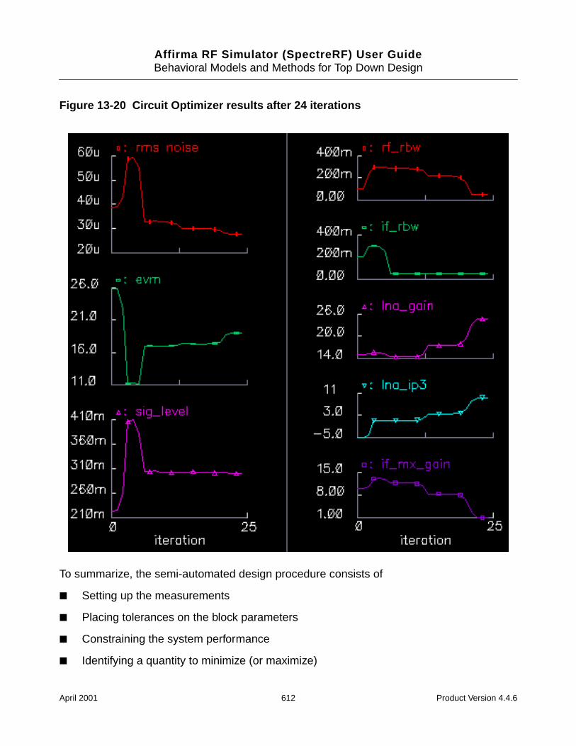
Affirma RF Simulator (SpectreRF) User GuideBehavioral Models and Methods for Top Down Design
Figure 13-20 Circuit Optimizer results after 24 iterations
To summarize, the semi-automated design procedure consists of
Setting up the measurements
Placing tolerances on the block parameters
Constraining the system performance
Identifying a quantity to minimize (or maximize)
April 2001 612 Product Version 4.4.6
Affirma RF Simulator (SpectreRF) User GuideBehavioral Models and Methods for Top Down Design
Running the Optimizer
Evaluating the results1.
Each simulation covers 100s, or about 80 CDMA symbols. The suppressed carriers are a2.14GHz RF carrier, an LO carrier at 2.354GHz, and an IF carrier at 214MHz. The symbolrate is 1.2288 Mega-symbols per second.
Each combined Transient and noise analysis runs in less than 3 minutes on an Ultra 1. Sixoptimizer iterations take between 1 and 2 hours depending the machine and the options.Based on run times from the BB_test_bench circuit, with Envelope Following analysis thesame six optimizer iterations would have taken over 6 days. With Spectre Transient theywould have taken over 2 months. There is no way either passband approach can optimizespecifications and tolerances in any reasonable amount of time.
Once the architecture is designed you can quickly create a passband view of the architecturalmodel2. The passband view checks for problems that escape the baseband view. Forexample, although the baseband view quickly assesses what filters do to the basebandsignal, baseband models do not indicate whether the filters are indeed removing undesiredcarrier harmonics. Baseband modeling is also not the best way to evaluate image rejection.Although the baseband model accurately simulates how the desired signal propagatesthrough an image rejection receiver, it does not accurately simulate how much of the imagesignal propagates to the receiver output.
The passband view also creates a system testbench as mentioned in the section on TopDown Design of RF Systems. The steps below show how to switch views and make an end-to-end RF measurement, the one dB compression point. The one dB compression point isusually a transmitter specification but it is better for demonstrating this flow because it iseasier to set up.
1. Copy the original receiver model from the Circuit Optimizer analysis to a new schematicwindow. Copy everything from the LNA to the low pass filters.
2. Edit the properties of the IQ_demodulator (IQ_demod_BB) to set the last parameter, flo,to “-frf+flo1”. The baseband view does not need the local oscillator frequency but thepassband view does.
1. This is why the process is called semi -automated. Upon evaluating results for the first orsecond time you will probably have to refine tolerances, refine goals, add or delete con-straints, add or delete variables.
2. In this release, the passband behavioral models in the top_dwnPB category and in thepassband view do not introduce any specifications that are not in the baseband models.Subsequent releases of the library may give the passband models the ability to introducenew specifications such as IIP2 and DC offsets.
April 2001 613 Product Version 4.4.6
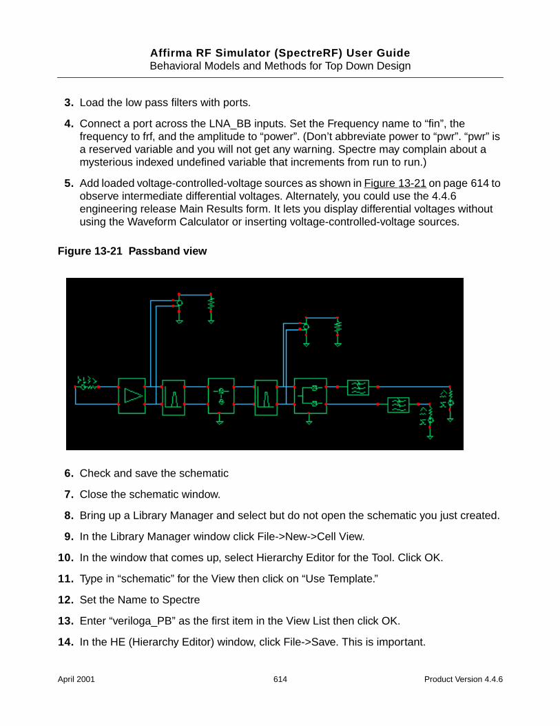
Affirma RF Simulator (SpectreRF) User GuideBehavioral Models and Methods for Top Down Design
3. Load the low pass filters with ports.
4. Connect a port across the LNA_BB inputs. Set the Frequency name to “fin”, thefrequency to frf, and the amplitude to “power”. (Don’t abbreviate power to “pwr”. “pwr” isa reserved variable and you will not get any warning. Spectre may complain about amysterious indexed undefined variable that increments from run to run.)
5. Add loaded voltage-controlled-voltage sources as shown in Figure 13-21 on page 614 toobserve intermediate differential voltages. Alternately, you could use the 4.4.6engineering release Main Results form. It lets you display differential voltages withoutusing the Waveform Calculator or inserting voltage-controlled-voltage sources.
Figure 13-21 Passband view
6. Check and save the schematic
7. Close the schematic window.
8. Bring up a Library Manager and select but do not open the schematic you just created.
9. In the Library Manager window click File->New->Cell View.
10. In the window that comes up, select Hierarchy Editor for the Tool. Click OK.
11. Type in “schematic” for the View then click on “Use Template.”
12. Set the Name to Spectre
13. Enter “veriloga_PB” as the first item in the View List then click OK.
14. In the HE (Hierarchy Editor) window, click File->Save. This is important.
April 2001 614 Product Version 4.4.6
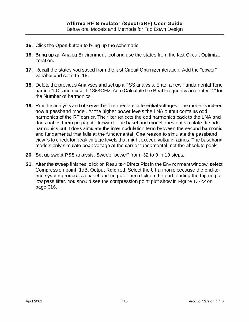
Affirma RF Simulator (SpectreRF) User GuideBehavioral Models and Methods for Top Down Design
15. Click the Open button to bring up the schematic.
16. Bring up an Analog Environment tool and use the states from the last Circuit Optimizeriteration.
17. Recall the states you saved from the last Circuit Optimizer iteration. Add the “power”variable and set it to -16.
18. Delete the previous Analyses and set up a PSS analysis. Enter a new Fundamental Tonenamed “LO” and make it 2.354GHz. Auto Calculate the Beat Frequency and enter “1” forthe Number of harmonics.
19. Run the analysis and observe the intermediate differential voltages. The model is indeednow a passband model. At the higher power levels the LNA output contains oddharmonics of the RF carrier. The filter reflects the odd harmonics back to the LNA anddoes not let them propagate forward. The baseband model does not simulate the oddharmonics but it does simulate the intermodulation term between the second harmonicand fundamental that falls at the fundamental. One reason to simulate the passbandview is to check for peak voltage levels that might exceed voltage ratings. The basebandmodels only simulate peak voltage at the carrier fundamental, not the absolute peak.
20. Set up swept PSS analysis. Sweep “power” from -32 to 0 in 10 steps.
21. After the sweep finishes, click on Results->Direct Plot in the Environment window, selectCompression point, 1dB, Output Referred. Select the 0 harmonic because the end-to-end system produces a baseband output. Then click on the port loading the top outputlow pass filter. You should see the compression point plot show in Figure 13-22 onpage 616.
April 2001 615 Product Version 4.4.6
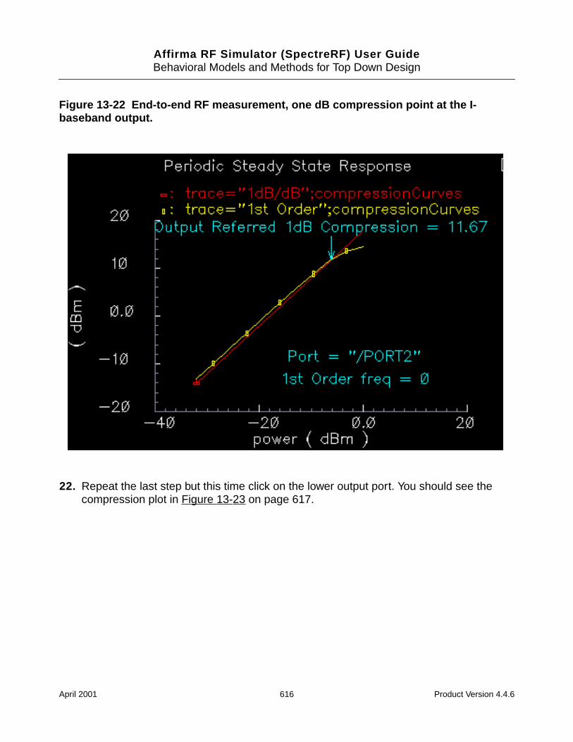
Affirma RF Simulator (SpectreRF) User GuideBehavioral Models and Methods for Top Down Design
Figure 13-22 End-to-end RF measurement, one dB compression point at the I-baseband output.
22. Repeat the last step but this time click on the lower output port. You should see thecompression plot in Figure 13-23 on page 617.
April 2001 616 Product Version 4.4.6
Affirma RF Simulator (SpectreRF) User GuideBehavioral Models and Methods for Top Down Design
Figure 13-23 End-to-end RF measurement, one dB compression point at the Q-baseband output.
You may wish to compare baseband and passband models. The next set of steps show youhow to set up a Transient analysis with the passband view and a Transient analysis with thebaseband view for direct comparison of baseband and passband models. You will run oneanalysis of the baseband view and two of the passband view. The second passband analysiswill be with tightened tolerances.
1. Save the passband schematic under a different name. You will use the new copy.
2. Repeat steps 9 through 17 from the last recipe for the new copy but do not enter the“veriloga_PB” view in the View List yet. You will do a baseband analysis first.
3. Delete the port driving the LNA.
4. You can also delete the loaded voltage-controlled-voltage sources.
5. You need to synthesize an antenna signal. Add an IQ_mod_BB from the top_dwnBBcategory. Set the I and Q gains to 0 dB. Set the 1dB compression points to 1000 so that
April 2001 617 Product Version 4.4.6
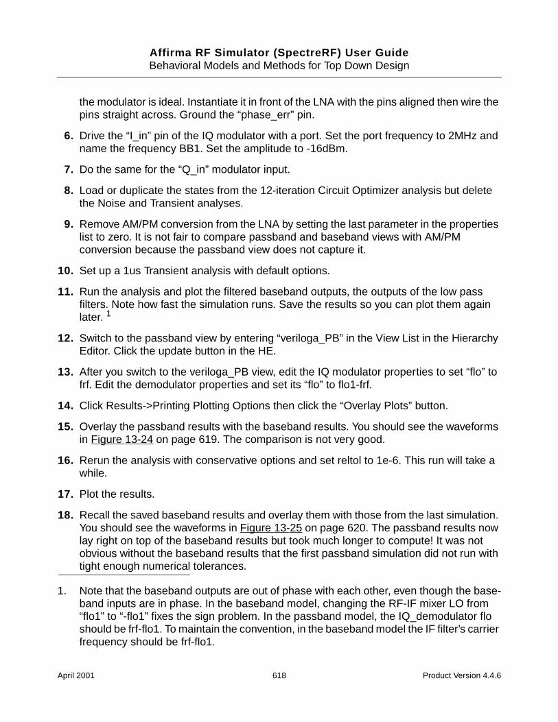
Affirma RF Simulator (SpectreRF) User GuideBehavioral Models and Methods for Top Down Design
the modulator is ideal. Instantiate it in front of the LNA with the pins aligned then wire thepins straight across. Ground the “phase_err” pin.
6. Drive the “I_in” pin of the IQ modulator with a port. Set the port frequency to 2MHz andname the frequency BB1. Set the amplitude to -16dBm.
7. Do the same for the “Q_in” modulator input.
8. Load or duplicate the states from the 12-iteration Circuit Optimizer analysis but deletethe Noise and Transient analyses.
9. Remove AM/PM conversion from the LNA by setting the last parameter in the propertieslist to zero. It is not fair to compare passband and baseband views with AM/PMconversion because the passband view does not capture it.
10. Set up a 1us Transient analysis with default options.
11. Run the analysis and plot the filtered baseband outputs, the outputs of the low passfilters. Note how fast the simulation runs. Save the results so you can plot them againlater. 1
12. Switch to the passband view by entering “veriloga_PB” in the View List in the HierarchyEditor. Click the update button in the HE.
13. After you switch to the veriloga_PB view, edit the IQ modulator properties to set “flo” tofrf. Edit the demodulator properties and set its “flo” to flo1-frf.
14. Click Results->Printing Plotting Options then click the “Overlay Plots” button.
15. Overlay the passband results with the baseband results. You should see the waveformsin Figure 13-24 on page 619. The comparison is not very good.
16. Rerun the analysis with conservative options and set reltol to 1e-6. This run will take awhile.
17. Plot the results.
18. Recall the saved baseband results and overlay them with those from the last simulation.You should see the waveforms in Figure 13-25 on page 620. The passband results nowlay right on top of the baseband results but took much longer to compute! It was notobvious without the baseband results that the first passband simulation did not run withtight enough numerical tolerances.
1. Note that the baseband outputs are out of phase with each other, even though the base-band inputs are in phase. In the baseband model, changing the RF-IF mixer LO from“flo1” to “-flo1” fixes the sign problem. In the passband model, the IQ_demodulator floshould be frf-flo1. To maintain the convention, in the baseband model the IF filter’s carrierfrequency should be frf-flo1.
April 2001 618 Product Version 4.4.6
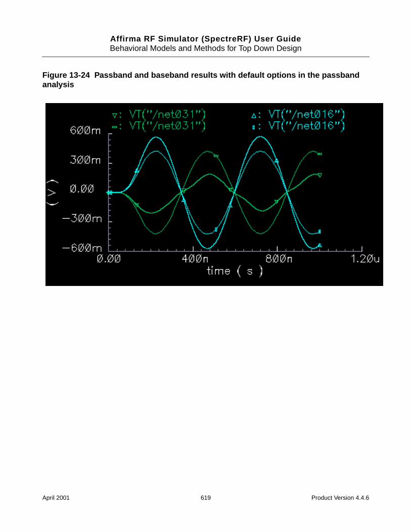
Affirma RF Simulator (SpectreRF) User GuideBehavioral Models and Methods for Top Down Design
Figure 13-24 Passband and baseband results with default options in the passbandanalysis
April 2001 619 Product Version 4.4.6
Affirma RF Simulator (SpectreRF) User GuideBehavioral Models and Methods for Top Down Design
Figure 13-25 Passband and baseband results with tighter options in the passbandanalysis
Relationship Between Baseband and Passband Noise
Noise analysis at baseband can be confusing because factors of two appear in a number ofplaces throughout the calculations. For example:
Each passband node becomes two equivalent baseband nodes.
Does noise injected at a passband node split between the two equivalent basebandnodes?
If so, does the noise split evenly?
As shown in the BB_test_bench example, baseband models simulate peak in-phase andpeak quadrature components of the carrier.
When analyzing signal-to-noise ratios, does that mean you have to use half the squareof the baseband signals?
April 2001 620 Product Version 4.4.6
Affirma RF Simulator (SpectreRF) User GuideBehavioral Models and Methods for Top Down Design
The Analog Artist displays single sided power spectral densities.
Since the baseband power spectral density is the two-sided passband density shifteddown, is there another factor of two because we can only see the baseband density forpositive frequencies?
White noise at the input of a mixer mixes up to the carrier from DC but there is also noiseat twice the carrier that mixers down to the carrier.
Does the baseband model account for this?
Before sorting out the factors of two, please note that baseband noise analysis is valid onlyfor small signals. If any element in the architecture operates in a non-linear fashion, the noiseanalysis might be inaccurate. This is due to the fact that a baseband noise analysis follows aDC operating point analysis, rather than a PSS analysis. Instantaneous incremental gain in apassband static non-linear model dithers at the carrier frequency. When the carrier swingsthrough zero, the incremental gain is large and noise at the input is amplified. When thecarrier reaches its peak and drives the circuit into saturation, the incremental gain is smaller.The average gain is greater than the minimum gain. The baseband model remains in the non-linear region because it only simulates peak voltages. Consequently, the incremental gain isalways a minimum and the baseband model under-estimates the amount of noisepropagating to the output. If the peak input signal drives the model into saturation be sure toscale the baseband noise results accordingly.
The circuit discussed here is called noise_test_circuit and you can find it in the rfExampleslibrary. The circuit looks as shown in Figure 13-26 on page 622.
April 2001 621 Product Version 4.4.6
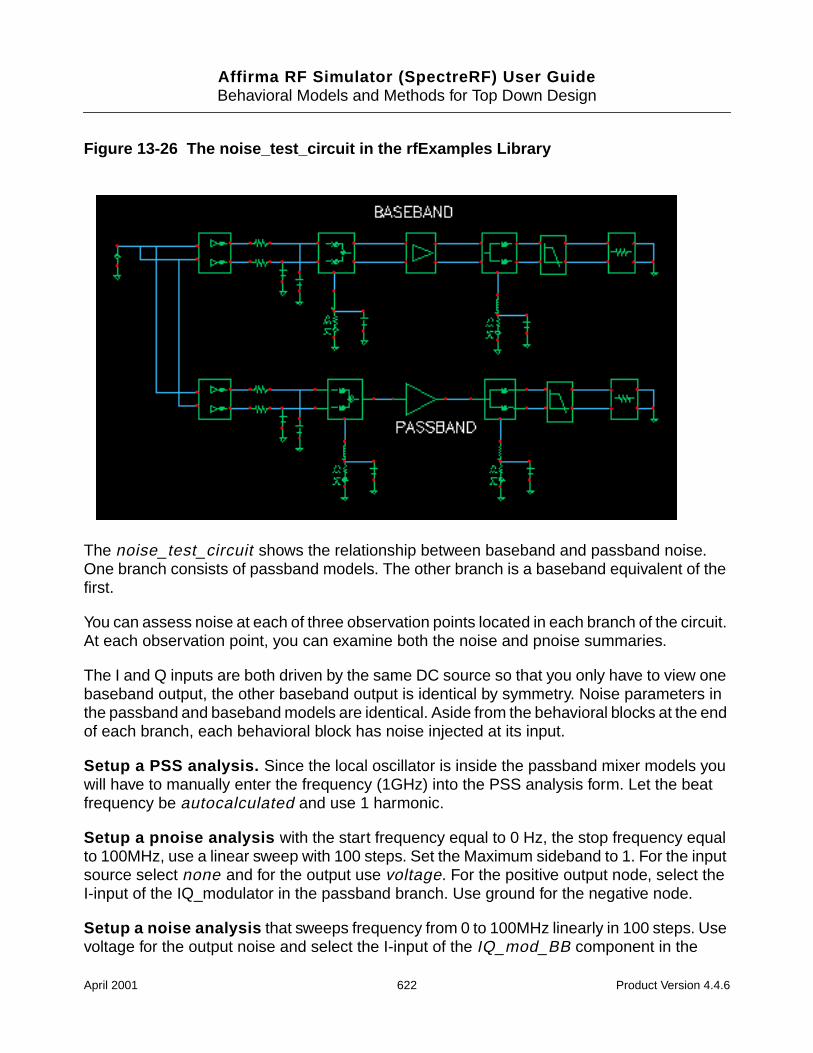
Affirma RF Simulator (SpectreRF) User GuideBehavioral Models and Methods for Top Down Design
Figure 13-26 The noise_test_circuit in the rfExamples Library
The noise_test_circuit shows the relationship between baseband and passband noise.One branch consists of passband models. The other branch is a baseband equivalent of thefirst.
You can assess noise at each of three observation points located in each branch of the circuit.At each observation point, you can examine both the noise and pnoise summaries.
The I and Q inputs are both driven by the same DC source so that you only have to view onebaseband output, the other baseband output is identical by symmetry. Noise parameters inthe passband and baseband models are identical. Aside from the behavioral blocks at the endof each branch, each behavioral block has noise injected at its input.
Setup a PSS analysis. Since the local oscillator is inside the passband mixer models youwill have to manually enter the frequency (1GHz) into the PSS analysis form. Let the beatfrequency be autocalculated and use 1 harmonic.
Setup a pnoise analysis with the start frequency equal to 0 Hz, the stop frequency equalto 100MHz, use a linear sweep with 100 steps. Set the Maximum sideband to 1. For the inputsource select none and for the output use voltage. For the positive output node, select theI-input of the IQ_modulator in the passband branch. Use ground for the negative node.
Setup a noise analysis that sweeps frequency from 0 to 100MHz linearly in 100 steps. Usevoltage for the output noise and select the I-input of the IQ_mod_BB component in the
April 2001 622 Product Version 4.4.6
Affirma RF Simulator (SpectreRF) User GuideBehavioral Models and Methods for Top Down Design
baseband branch for the positive node. Select ground for the negative node. Set the inputnoise port to any one of the ports in the circuit. Noise from that port will not affect eitherpassband nor baseband branches.
Run the analysis.
When the analysis finishes, go to the Analog Artist simulation window and click on results-print-pss noise summary.
In the form that appears, include All types, set Type to integrated noise, look at noise from0 to 100MHz, select “truncate by number", and view the top 2 noise contributors. There areonly 2 noise contributors at this point, noise at the I/Q inputs and noise from the low passresistors.
Now print the noise summary. (This is different from the pnoise summary.) Again, printintegrated noise (from 0 to 100MHz). Select All types and print noise from the top 2 noisecontributors.
Figure 13-27 on page 624 shows the noise summaries. The two summaries agree becauseat this point in the circuit, both nodes are really baseband nodes.
April 2001 623 Product Version 4.4.6
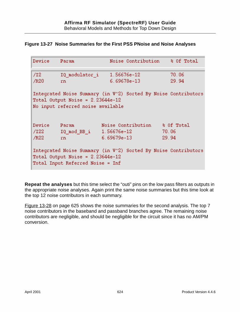
Affirma RF Simulator (SpectreRF) User GuideBehavioral Models and Methods for Top Down Design
Figure 13-27 Noise Summaries for the First PSS PNoise and Noise Analyses
Repeat the analyses but this time select the “outi” pins on the low pass filters as outputs inthe appropriate noise analyses. Again print the same noise summaries but this time look atthe top 12 noise contributors in each summary.
Figure 13-28 on page 625 shows the noise summaries for the second analysis. The top 7noise contributors in the baseband and passband branches agree. The remaining noisecontributors are negligible, and should be negligible for the circuit since it has no AM/PMconversion.
April 2001 624 Product Version 4.4.6
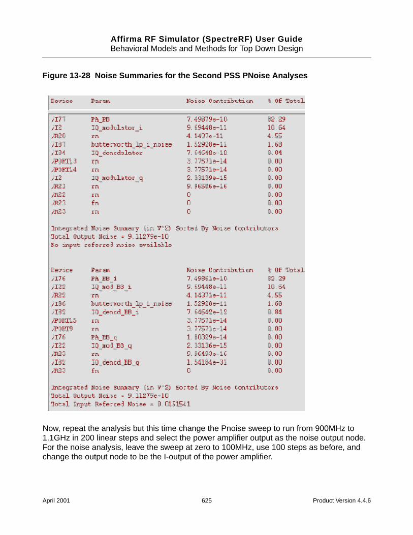
Affirma RF Simulator (SpectreRF) User GuideBehavioral Models and Methods for Top Down Design
Figure 13-28 Noise Summaries for the Second PSS PNoise Analyses
Now, repeat the analysis but this time change the Pnoise sweep to run from 900MHz to1.1GHz in 200 linear steps and select the power amplifier output as the noise output node.For the noise analysis, leave the sweep at zero to 100MHz, use 100 steps as before, andchange the output node to be the I-output of the power amplifier.
April 2001 625 Product Version 4.4.6
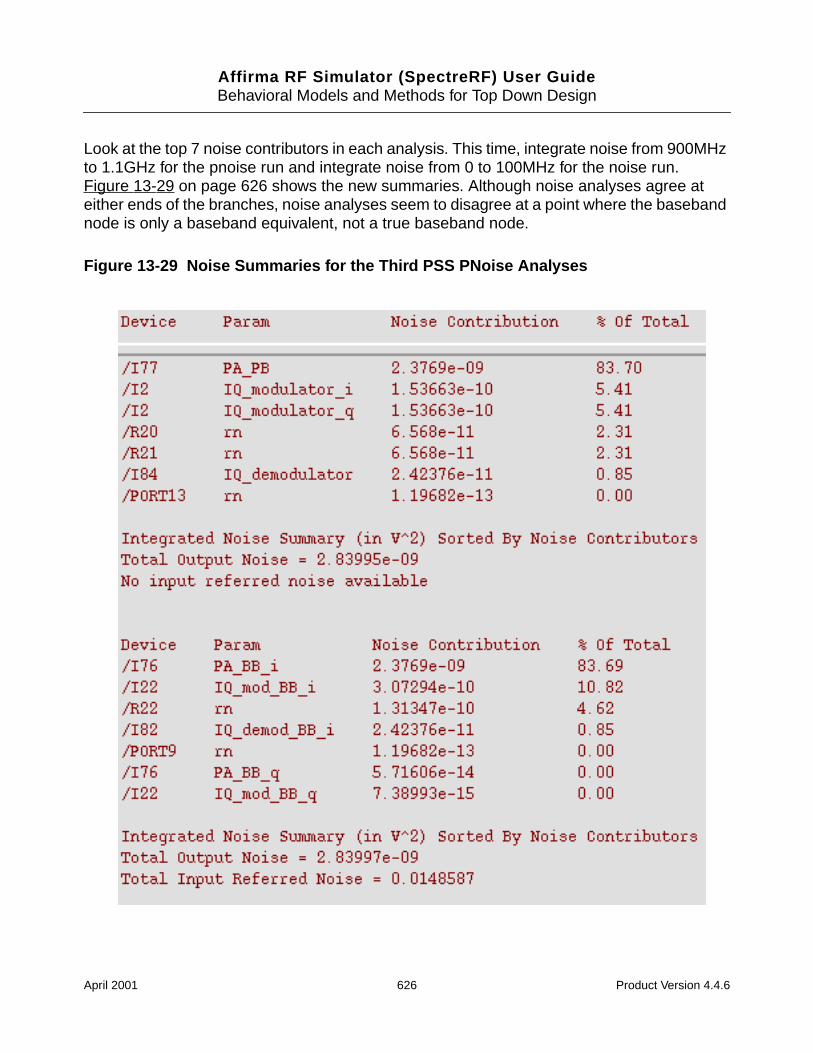
Affirma RF Simulator (SpectreRF) User GuideBehavioral Models and Methods for Top Down Design
Look at the top 7 noise contributors in each analysis. This time, integrate noise from 900MHzto 1.1GHz for the pnoise run and integrate noise from 0 to 100MHz for the noise run.Figure 13-29 on page 626 shows the new summaries. Although noise analyses agree ateither ends of the branches, noise analyses seem to disagree at a point where the basebandnode is only a baseband equivalent, not a true baseband node.
Figure 13-29 Noise Summaries for the Third PSS PNoise Analyses
April 2001 626 Product Version 4.4.6
Affirma RF Simulator (SpectreRF) User GuideBehavioral Models and Methods for Top Down Design
The apparent disagreement shown in Figure 13-29 on page 626 requires an explanation. Letus examine the noise contributors and try to answer some the questions we posed earlier.
Noise at the power amplifier output due to noise injected at a passband node:
Passband model contributors: PA_PB and IQ_demodulator, port 9.
Baseband model contributors: PA_BB_i, IQ_demod_BB_i, port 13.
Passband and baseband counterparts contribute the same amount of noise. However, in thebaseband model, from symmetry you see the same numbers if you look at the Q-node. Thismeans the baseband model predicts twice as much total noise due to noise injected betweenthe modulators.
This factor of two is intentionally introduced to maintain the correct signal-to-noise ratio. Thebaseband model simulates peak signals; the carrier is suppressed. Without the carrier, signalpower equals the square of the peak rather than one half of the square. This factor of two isnot as arbitrary as it seems. The baseband model predicts the correct noise afterdemodulation because the passband demodulator model includes an extra factor of two tooffset the factor of two inherent in the demodulation process.
Let the modulated carrier be i(t)*cos(wc*t) -q(t)*sin(wc*t) + noise(t) .
Now consider the I-output. To generate the I-output, the demodulator multiplies the signal bycos(wc*t) . The only part that propagates through the subsequent filter is (1/2)i(t) +noise(t)*cos(wc*t) . To recover i(t) , the passband demodulator model must scale thissum by two. (The baseband demodulator does not need to scale by two to extract thebaseband signal because the carrier is suppressed.)
Thus, noise at passband demodulator model output equals 2*noise(t)*cos(wc*t) . Thefiltered noise power density is then 4*( input noise density )/2 . 1 The filtered outputnoise density is twice the input noise density.
In the baseband model, doubling the noise injected at the passband nodes was not simply amatter of convenience.
So, to answer questions 1 and 2
Yes, noise injected at a passband node splits evenly between the two equivalentbaseband nodes
but
1. The factor of 1/2 comes from the cosine.
April 2001 627 Product Version 4.4.6
Affirma RF Simulator (SpectreRF) User GuideBehavioral Models and Methods for Top Down Design
Since each split is doubled, the ratio of peak signal to total noise equals the true signal-to-noise ratio.
Question 3 is rendered moot by using the noise summary and integrating over the properband. If the pnoise analysis only integrated from 1GHz to 1.1GHz, (instead of from 900MHzto 1.1GHz), there would be a mysterious factor of two error.
In the baseband model, phase noise entering on the phase error pin propagates to both theI and Q outputs. In the baseband model, the same noise power appears on just the oneoutput. Again, the total noise in the baseband model is twice that of the passband model tomaintain the correct signal-to-noise ratio.
Noise injected at the modulator input (resistors and modulator noise):
Total noise in the baseband model due to modulator and input resistor noise is twice what itis from just one phase. Thus, the total noise due to sources on the input sides of themodulators differ by a factor of two. This occurs because the passband model is a realmultiplier, which modulates the noise. If the peak signal voltage agrees with the basebandmodel, the passband modulator model attenuates input noise most of the time. The importantthing is that the signal-to-noise ratios in the passband and baseband models agree anywherein the system.
Now, copy the circuit so you can remove the capacitors at the modulator inputs andrepeat the last set of noise analyses. You will see that in the passband model, the inputresistors, R20 and R21, together contribute twice as much as the baseband counterpart,R22. With the capacitors, R20 and R21 together contribute just as much as R22. Without thecapacitors, the input noise is truly white over the frequencies of interest. The same thinghappens to the modulator noise itself. Figure 13-30 on page 629 shows the results.
In particular, the modulator now also has noise at twice the carrier frequency and thatnoise mixes down to the carrier frequency. The baseband model is just that, a basebandmodel. The answer to question 4 is no. The baseband models do not account for noise, orsignals, at carrier harmonics. The baseband equivalent noise analysis is valid only if noiseinjected into the modulators has no power beyond the local oscillator frequency. Phase noiseinjected at the phase noise pins should also be band limited.
April 2001 628 Product Version 4.4.6
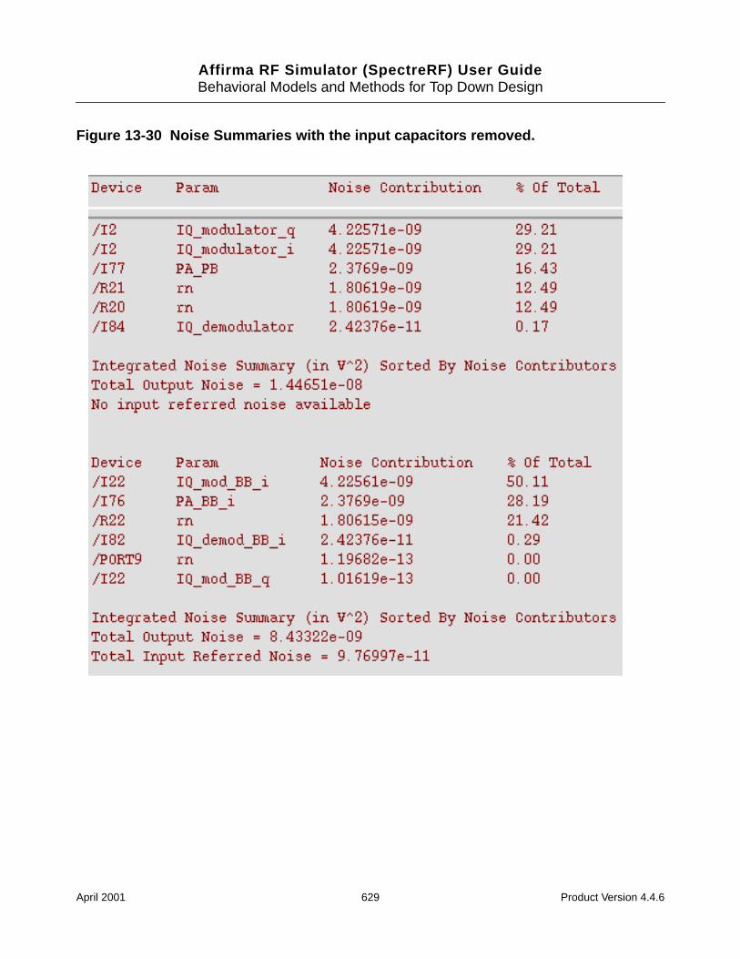
Affirma RF Simulator (SpectreRF) User GuideBehavioral Models and Methods for Top Down Design
Figure 13-30 Noise Summaries with the input capacitors removed.
April 2001 629 Product Version 4.4.6
Affirma RF Simulator (SpectreRF) User GuideBehavioral Models and Methods for Top Down Design
unda-e fun-t
near de-condes and
Baseband Library
This section explains a few assumptions and measurements common to several elements inthe baseband library. Except for AM/PM conversion, all model specifications are defined bymeasurements on the passband models. Most baseband models have a differentialpassband view. Those that do not have a passband view are meant only for baseband use.The models in the top_dwnPB category are singled ended versions of the differentialpassband views. The single-ended passband models are used to describe themeasurements but the measurements also apply to the differential versions.
Assumptions
All behavioral models require assumptions and the top-down models at hand are noexception. The assumptions are summarized below:
The non-linear RF components are memoryless.
Noise in the models is white additive Gaussian noise split equally between the two outputpins. I and Q noise sources in any model are uncorrelated.
Except for loading effects, signal flow is unilateral.
Terminal impedances are purely resistive.
The following is a single assumption stated three ways:
Only third order non-linearities matter; no even order non-linearity matters.
Harmonics of the carrier between any two baseband models is negligible
Baseband models need not simulate IP2 1 or DC offsets.
All mixers, including those in modulators and demodulators, can be modeled as a staticnon-linearity followed by an ideal multiplier.
All local oscillators are sinusoidal.
1.The basic problem is that "even" non-linearities do not produce output power at the carrier fmental. Baseband models only model effects like IP3 because third order distortion affects thdamental. Second order distortion only affects the fundamental at the output of a subsequencascaded non-linear device. You can build one baseband model of the two cascaded non-livices and simulate how second order distortion in the first device affects the output of the sedevice at the fundamental. You can not cascade individual baseband models of the two devicobserve any second order effects.
April 2001 630 Product Version 4.4.6
Affirma RF Simulator (SpectreRF) User GuideBehavioral Models and Methods for Top Down Design
Compatibility
All baseband models except the baseband signal generators and instrumentation blocksare compatible with SpectreRF.
All models are written in Verilog-A.
Library Categories
The rfLib has six categories.
1. Original_RFAHDL_lib: This the original RF AHDL library originally released in 4.4.3. Itis documented in Appendix D.
2. bot_upBB : This category contains only the J-models in this release.
3. measurement: This category contains models used to make measurements andincludes the instrumentation blocks and baseband signal generators. They are not partof an RF architecture. These models only facilitate measurements and diagnostics.
4. testbenches: This category contains the test circuits mentioned in this document whendefining model specifications. Where possible, the models are specified in terms ofstandard RF measurements. The most precise way to describe a measurement is with atest circuit, set up instructions, and sample measurements. The circuits in this categoryserve that purpose.
5. top_dwnBB: This category contains models of common architectural function blocks.The default view of the models in this category is the baseband view but all models inthis category have a differential passband view called “veriloga_PB”. The onlyexceptions are the BB_loss and VGA_BB models. The BB_loss model is meant only forbaseband analysis. The VGA_BB is an engineering release of a variable gain amplifier.It is not documented or supported in this release and is subject to change in futurereleases.
6. top_dwnPB: This category contains single-ended passband versions of the basebandmodels.
Inputs and Outputs on Baseband Models
Except where noted, all baseband models have inputs and outputs as shown in Figure 13-31on page 632. Do not confuse the baseband models with two-port S-parameter models.
April 2001 631 Product Version 4.4.6
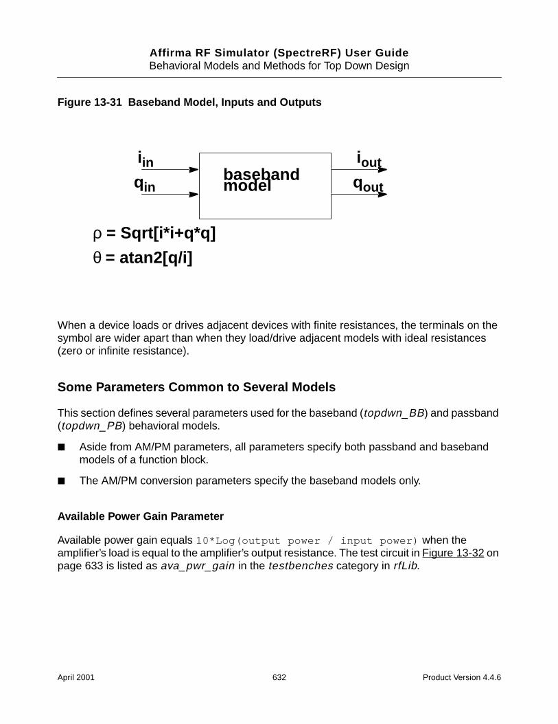
Affirma RF Simulator (SpectreRF) User GuideBehavioral Models and Methods for Top Down Design
Figure 13-31 Baseband Model, Inputs and Outputs
When a device loads or drives adjacent devices with finite resistances, the terminals on thesymbol are wider apart than when they load/drive adjacent models with ideal resistances(zero or infinite resistance).
Some Parameters Common to Several Models
This section defines several parameters used for the baseband (topdwn_BB) and passband(topdwn_PB) behavioral models.
Aside from AM/PM parameters, all parameters specify both passband and basebandmodels of a function block.
The AM/PM conversion parameters specify the baseband models only.
Available Power Gain Parameter
Available power gain equals 10*Log(output power / input power) when theamplifier’s load is equal to the amplifier’s output resistance. The test circuit in Figure 13-32 onpage 633 is listed as ava_pwr_gain in the testbenches category in rfLib.
basebandmodel
iinqin
iout
qout
ρ = Sqrt[i*i+q*q]
θ = atan2[q/i]
April 2001 632 Product Version 4.4.6
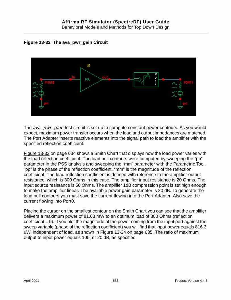
Affirma RF Simulator (SpectreRF) User GuideBehavioral Models and Methods for Top Down Design
Figure 13-32 The ava_pwr_gain Circuit
The ava_pwr_gain test circuit is set up to compute constant power contours. As you wouldexpect, maximum power transfer occurs when the load and output impedances are matched.The Port Adapter inserts reactive elements into the signal path to load the amplifier with thespecified reflection coefficient.
Figure 13-33 on page 634 shows a Smith Chart that displays how the load power varies withthe load refection coefficient. The load pull contours were computed by sweeping the “pp”parameter in the PSS analysis and sweeping the “mm” parameter with the Parametric Tool.“pp” is the phase of the reflection coefficient. “mm” is the magnitude of the reflectioncoefficient. The load reflection coefficient is defined with reference to the amplifier outputresistance, which is 300 Ohms in this case. The amplifier input resistance is 20 Ohms. Theinput source resistance is 50 Ohms. The amplifier 1dB compression point is set high enoughto make the amplifier linear. The available power gain parameter is 20 dB. To generate theload pull contours you must save the current flowing into the Port Adapter. Also save thecurrent flowing into Port0.
Placing the cursor on the smallest contour on the Smith Chart you can see that the amplifierdelivers a maximum power of 81.63 mW to an optimum load of 300 Ohms (reflectioncoefficient = 0). If you plot the magnitude of the power coming from the input port against thesweep variable (phase of the reflection coefficient) you will find that input power equals 816.3uW, independent of load, as shown in Figure 13-34 on page 635. The ratio of maximumoutput to input power equals 100, or 20 dB, as specified.
April 2001 633 Product Version 4.4.6
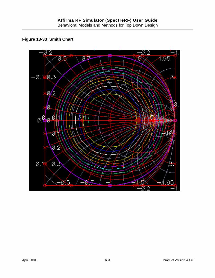
Affirma RF Simulator (SpectreRF) User GuideBehavioral Models and Methods for Top Down Design
Figure 13-33 Smith Chart
April 2001 634 Product Version 4.4.6
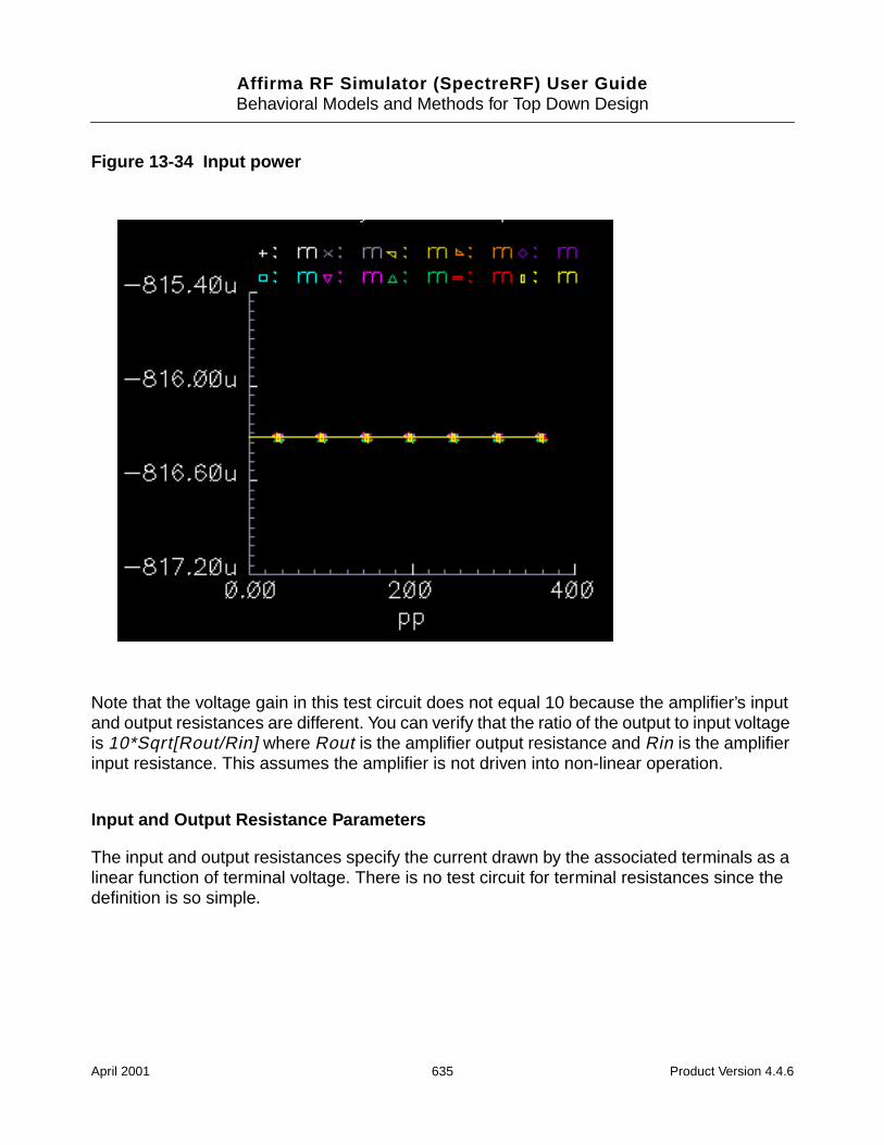
Affirma RF Simulator (SpectreRF) User GuideBehavioral Models and Methods for Top Down Design
Figure 13-34 Input power
Note that the voltage gain in this test circuit does not equal 10 because the amplifier’s inputand output resistances are different. You can verify that the ratio of the output to input voltageis 10*Sqrt[Rout/Rin] where Rout is the amplifier output resistance and Rin is the amplifierinput resistance. This assumes the amplifier is not driven into non-linear operation.
Input and Output Resistance Parameters
The input and output resistances specify the current drawn by the associated terminals as alinear function of terminal voltage. There is no test circuit for terminal resistances since thedefinition is so simple.
April 2001 635 Product Version 4.4.6
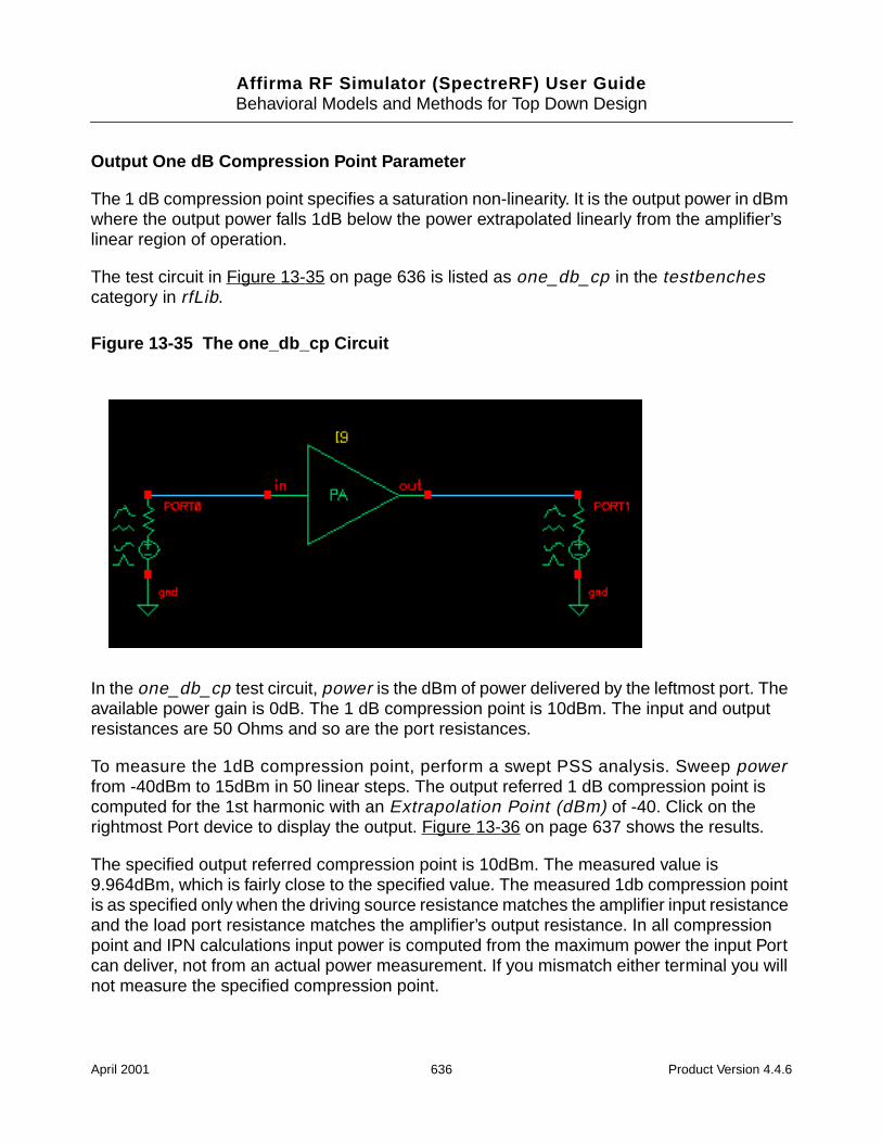
Affirma RF Simulator (SpectreRF) User GuideBehavioral Models and Methods for Top Down Design
Output One dB Compression Point Parameter
The 1 dB compression point specifies a saturation non-linearity. It is the output power in dBmwhere the output power falls 1dB below the power extrapolated linearly from the amplifier’slinear region of operation.
The test circuit in Figure 13-35 on page 636 is listed as one_db_cp in the testbenchescategory in rfLib.
Figure 13-35 The one_db_cp Circuit
In the one_db_cp test circuit, power is the dBm of power delivered by the leftmost port. Theavailable power gain is 0dB. The 1 dB compression point is 10dBm. The input and outputresistances are 50 Ohms and so are the port resistances.
To measure the 1dB compression point, perform a swept PSS analysis. Sweep powerfrom -40dBm to 15dBm in 50 linear steps. The output referred 1 dB compression point iscomputed for the 1st harmonic with an Extrapolation Point (dBm) of -40. Click on therightmost Port device to display the output. Figure 13-36 on page 637 shows the results.
The specified output referred compression point is 10dBm. The measured value is9.964dBm, which is fairly close to the specified value. The measured 1db compression pointis as specified only when the driving source resistance matches the amplifier input resistanceand the load port resistance matches the amplifier’s output resistance. In all compressionpoint and IPN calculations input power is computed from the maximum power the input Portcan deliver, not from an actual power measurement. If you mismatch either terminal you willnot measure the specified compression point.
April 2001 636 Product Version 4.4.6
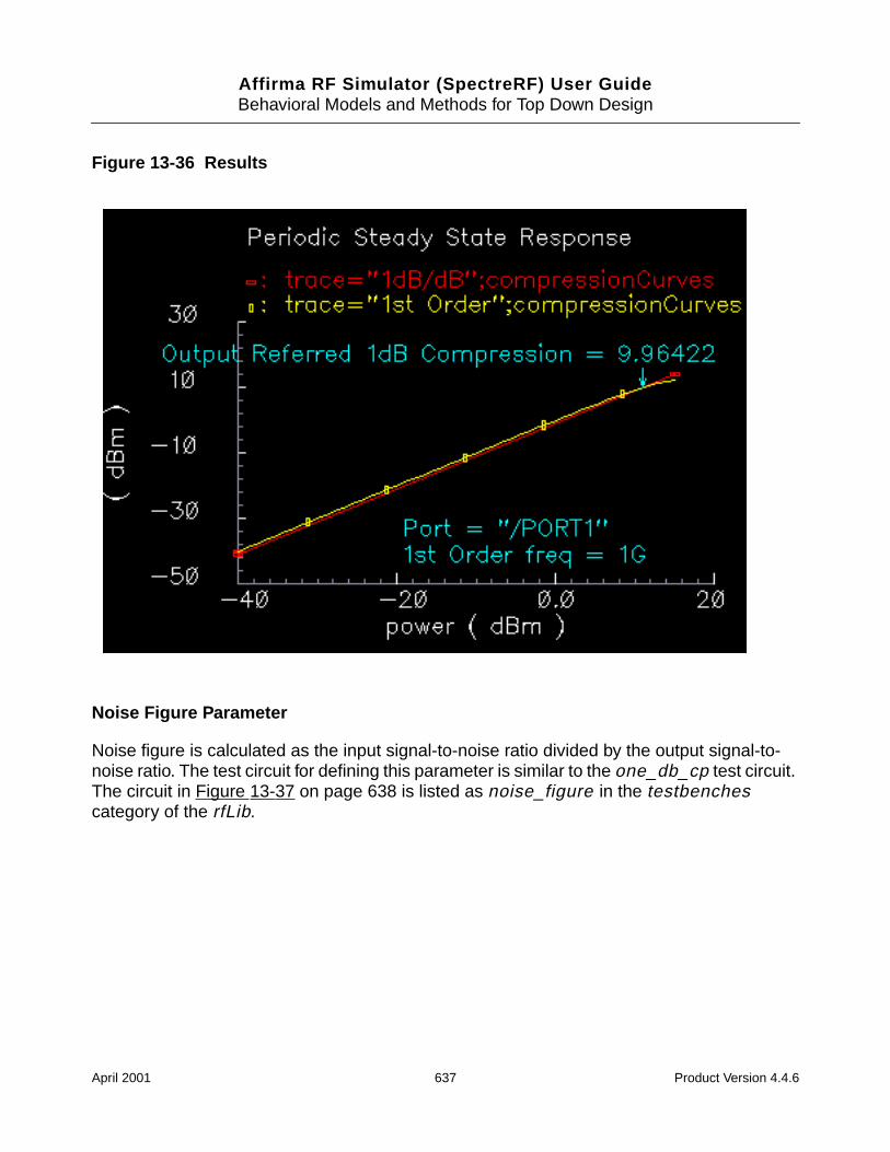
Affirma RF Simulator (SpectreRF) User GuideBehavioral Models and Methods for Top Down Design
Figure 13-36 Results
Noise Figure Parameter
Noise figure is calculated as the input signal-to-noise ratio divided by the output signal-to-noise ratio. The test circuit for defining this parameter is similar to the one_db_cp test circuit.The circuit in Figure 13-37 on page 638 is listed as noise_figure in the testbenchescategory of the rfLib.
April 2001 637 Product Version 4.4.6
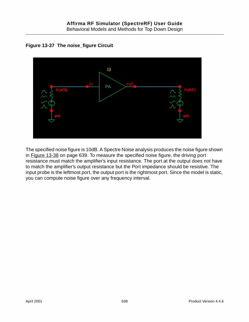
Affirma RF Simulator (SpectreRF) User GuideBehavioral Models and Methods for Top Down Design
Figure 13-37 The noise_figure Circuit
The specified noise figure is 10dB. A Spectre Noise analysis produces the noise figure shownin Figure 13-38 on page 639. To measure the specified noise figure, the driving portresistance must match the amplifier’s input resistance. The port at the output does not haveto match the amplifier’s output resistance but the Port impedance should be resistive. Theinput probe is the leftmost port, the output port is the rightmost port. Since the model is static,you can compute noise figure over any frequency interval.
April 2001 638 Product Version 4.4.6
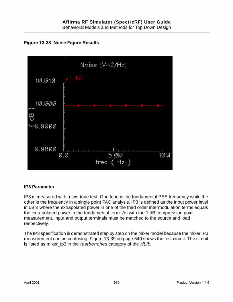
Affirma RF Simulator (SpectreRF) User GuideBehavioral Models and Methods for Top Down Design
Figure 13-38 Noise Figure Results
IP3 Parameter
IP3 is measured with a two-tone test. One tone is the fundamental PSS frequency while theother is the frequency in a single point PAC analysis. IP3 is defined as the input power levelin dBm where the extrapolated power in one of the third order intermodulation terms equalsthe extrapolated power in the fundamental term. As with the 1 dB compression pointmeasurement, input and output terminals must be matched to the source and loadrespectively.
The IP3 specification is demonstrated step by step on the mixer model because the mixer IP3measurement can be confusing. Figure 13-39 on page 640 shows the test circuit. The circuitis listed as mixer_ip3 in the testbenches category of the rfLib.
April 2001 639 Product Version 4.4.6
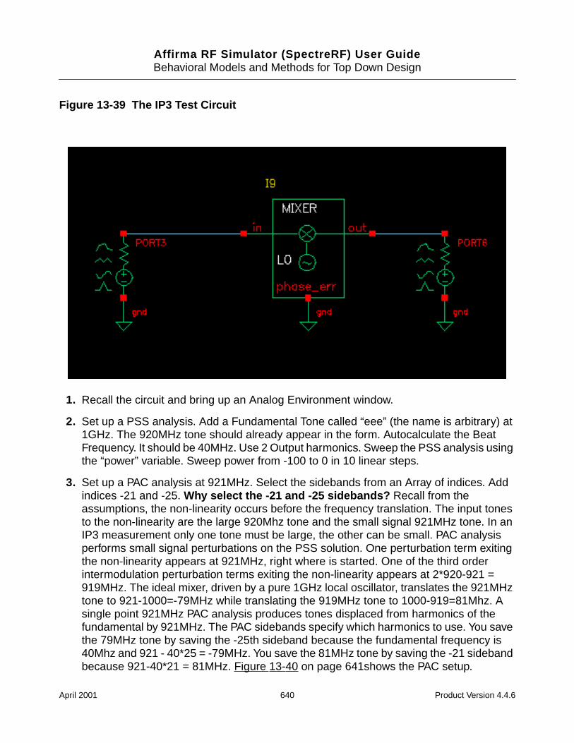
Affirma RF Simulator (SpectreRF) User GuideBehavioral Models and Methods for Top Down Design
Figure 13-39 The IP3 Test Circuit
1. Recall the circuit and bring up an Analog Environment window.
2. Set up a PSS analysis. Add a Fundamental Tone called “eee” (the name is arbitrary) at1GHz. The 920MHz tone should already appear in the form. Autocalculate the BeatFrequency. It should be 40MHz. Use 2 Output harmonics. Sweep the PSS analysis usingthe “power” variable. Sweep power from -100 to 0 in 10 linear steps.
3. Set up a PAC analysis at 921MHz. Select the sidebands from an Array of indices. Addindices -21 and -25. Why select the -21 and -25 sidebands? Recall from theassumptions, the non-linearity occurs before the frequency translation. The input tonesto the non-linearity are the large 920Mhz tone and the small signal 921MHz tone. In anIP3 measurement only one tone must be large, the other can be small. PAC analysisperforms small signal perturbations on the PSS solution. One perturbation term exitingthe non-linearity appears at 921MHz, right where is started. One of the third orderintermodulation perturbation terms exiting the non-linearity appears at 2*920-921 =919MHz. The ideal mixer, driven by a pure 1GHz local oscillator, translates the 921MHztone to 921-1000=-79MHz while translating the 919MHz tone to 1000-919=81Mhz. Asingle point 921MHz PAC analysis produces tones displaced from harmonics of thefundamental by 921MHz. The PAC sidebands specify which harmonics to use. You savethe 79MHz tone by saving the -25th sideband because the fundamental frequency is40Mhz and 921 - 40*25 = -79MHz. You save the 81MHz tone by saving the -21 sidebandbecause 921-40*21 = 81MHz. Figure 13-40 on page 641shows the PAC setup.
April 2001 640 Product Version 4.4.6
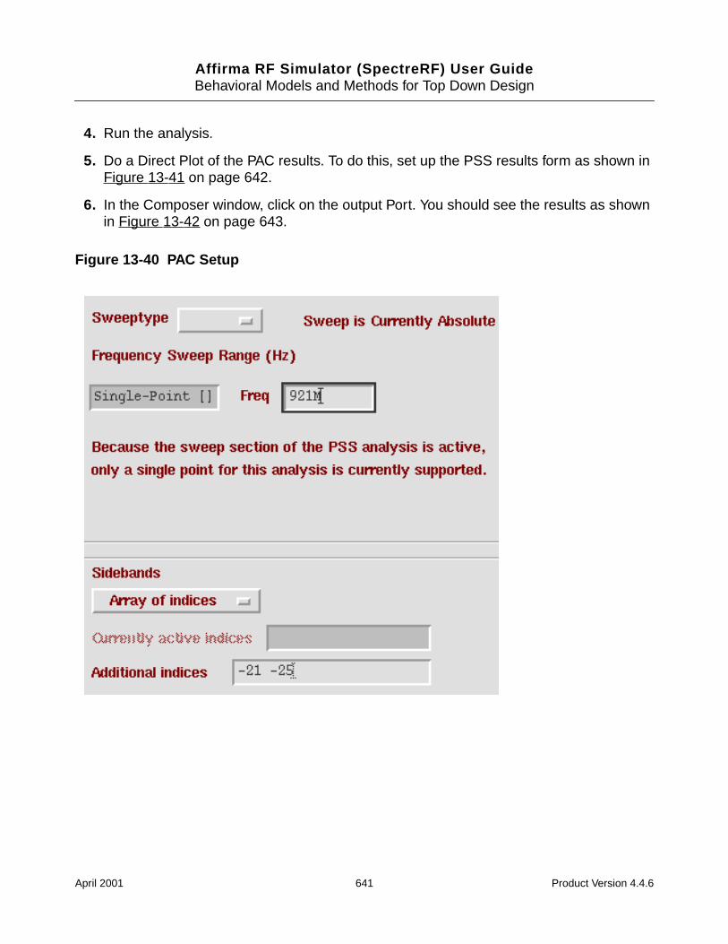
Affirma RF Simulator (SpectreRF) User GuideBehavioral Models and Methods for Top Down Design
4. Run the analysis.
5. Do a Direct Plot of the PAC results. To do this, set up the PSS results form as shown inFigure 13-41 on page 642.
6. In the Composer window, click on the output Port. You should see the results as shownin Figure 13-42 on page 643.
Figure 13-40 PAC Setup
April 2001 641 Product Version 4.4.6
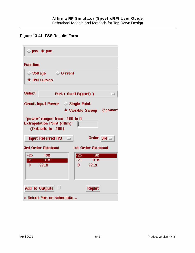
Affirma RF Simulator (SpectreRF) User GuideBehavioral Models and Methods for Top Down Design
Figure 13-41 PSS Results Form
April 2001 642 Product Version 4.4.6
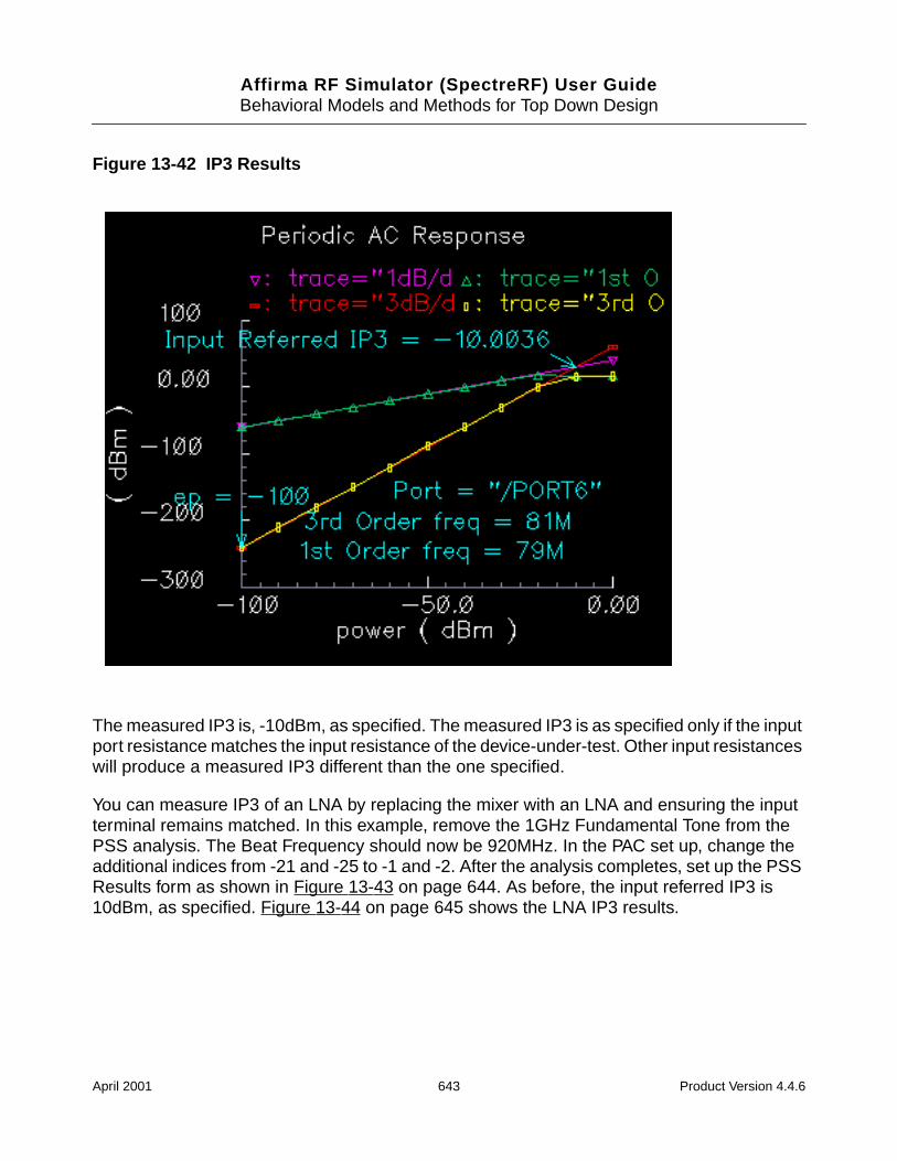
Affirma RF Simulator (SpectreRF) User GuideBehavioral Models and Methods for Top Down Design
Figure 13-42 IP3 Results
The measured IP3 is, -10dBm, as specified. The measured IP3 is as specified only if the inputport resistance matches the input resistance of the device-under-test. Other input resistanceswill produce a measured IP3 different than the one specified.
You can measure IP3 of an LNA by replacing the mixer with an LNA and ensuring the inputterminal remains matched. In this example, remove the 1GHz Fundamental Tone from thePSS analysis. The Beat Frequency should now be 920MHz. In the PAC set up, change theadditional indices from -21 and -25 to -1 and -2. After the analysis completes, set up the PSSResults form as shown in Figure 13-43 on page 644. As before, the input referred IP3 is10dBm, as specified. Figure 13-44 on page 645 shows the LNA IP3 results.
April 2001 643 Product Version 4.4.6
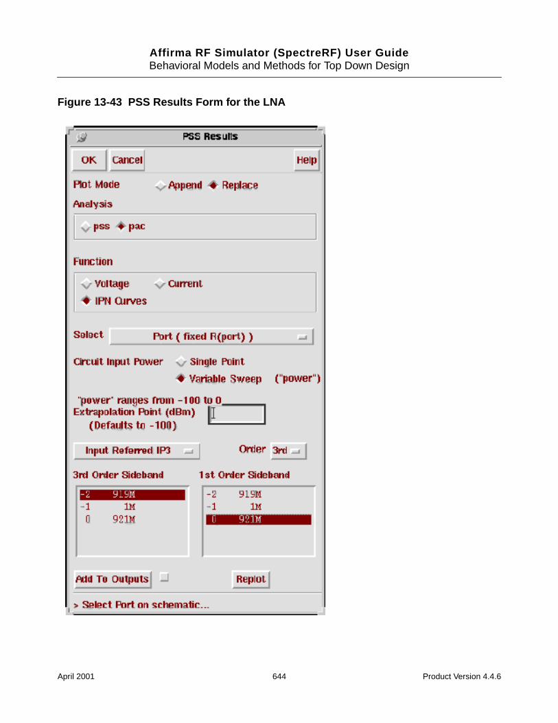
Affirma RF Simulator (SpectreRF) User GuideBehavioral Models and Methods for Top Down Design
Figure 13-43 PSS Results Form for the LNA
April 2001 644 Product Version 4.4.6
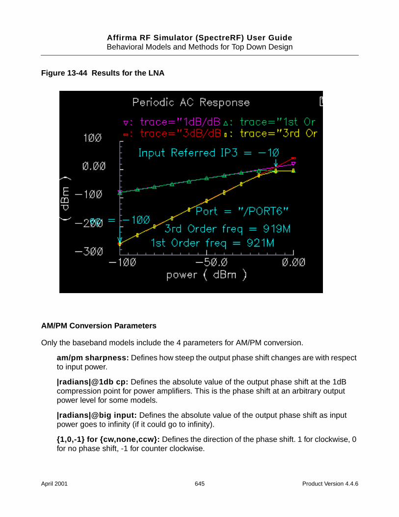
Affirma RF Simulator (SpectreRF) User GuideBehavioral Models and Methods for Top Down Design
Figure 13-44 Results for the LNA
AM/PM Conversion Parameters
Only the baseband models include the 4 parameters for AM/PM conversion.
am/pm sharpness: Defines how steep the output phase shift changes are with respectto input power.
|radians|@1db cp: Defines the absolute value of the output phase shift at the 1dBcompression point for power amplifiers. This is the phase shift at an arbitrary outputpower level for some models.
|radians|@big input: Defines the absolute value of the output phase shift as inputpower goes to infinity (if it could go to infinity).
1,0,-1 for cw,none,ccw: Defines the direction of the phase shift. 1 for clockwise, 0for no phase shift, -1 for counter clockwise.
April 2001 645 Product Version 4.4.6
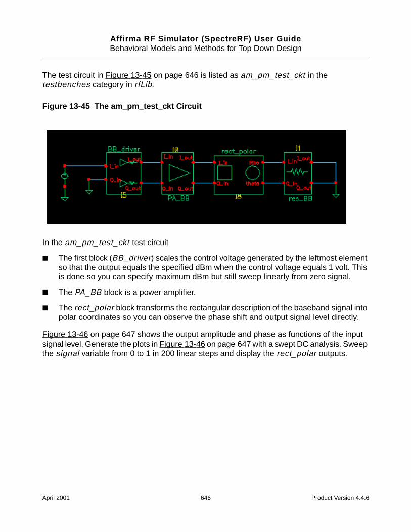
Affirma RF Simulator (SpectreRF) User GuideBehavioral Models and Methods for Top Down Design
The test circuit in Figure 13-45 on page 646 is listed as am_pm_test_ckt in thetestbenches category in rfLib.
Figure 13-45 The am_pm_test_ckt Circuit
In the am_pm_test_ckt test circuit
The first block (BB_driver) scales the control voltage generated by the leftmost elementso that the output equals the specified dBm when the control voltage equals 1 volt. Thisis done so you can specify maximum dBm but still sweep linearly from zero signal.
The PA_BB block is a power amplifier.
The rect_polar block transforms the rectangular description of the baseband signal intopolar coordinates so you can observe the phase shift and output signal level directly.
Figure 13-46 on page 647 shows the output amplitude and phase as functions of the inputsignal level. Generate the plots in Figure 13-46 on page 647 with a swept DC analysis. Sweepthe signal variable from 0 to 1 in 200 linear steps and display the rect_polar outputs.
April 2001 646 Product Version 4.4.6
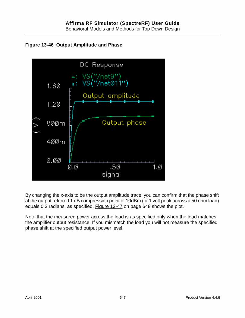
Affirma RF Simulator (SpectreRF) User GuideBehavioral Models and Methods for Top Down Design
Figure 13-46 Output Amplitude and Phase
By changing the x-axis to be the output amplitude trace, you can confirm that the phase shiftat the output referred 1 dB compression point of 10dBm (or 1 volt peak across a 50 ohm load)equals 0.3 radians, as specified. Figure 13-47 on page 648 shows the plot.
Note that the measured power across the load is as specified only when the load matchesthe amplifier output resistance. If you mismatch the load you will not measure the specifiedphase shift at the specified output power level.
April 2001 647 Product Version 4.4.6
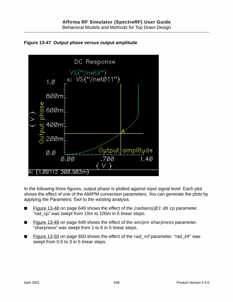
Affirma RF Simulator (SpectreRF) User GuideBehavioral Models and Methods for Top Down Design
Figure 13-47 Output phase versus output amplitude
In the following three figures, output phase is plotted against input signal level. Each plotshows the effect of one of the AM/PM conversion parameters. You can generate the plots byapplying the Parametric Tool to the existing analysis.
Figure 13-48 on page 649 shows the effect of the |radians|@1 db cp parameter.“rad_cp” was swept from 10m to 100m in 5 linear steps.
Figure 13-49 on page 649 shows the effect of the am/pm sharpness parameter.“sharpness” was swept from 1 to 6 in 5 linear steps.
Figure 13-50 on page 650 shows the effect of the rad_inf parameter. “rad_inf” wasswept from 0.5 to 3 in 5 linear steps.
April 2001 648 Product Version 4.4.6
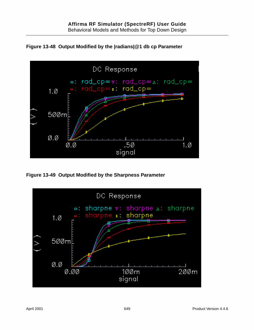
Affirma RF Simulator (SpectreRF) User GuideBehavioral Models and Methods for Top Down Design
Figure 13-48 Output Modified by the |radians|@1 db cp Parameter
Figure 13-49 Output Modified by the Sharpness Parameter
April 2001 649 Product Version 4.4.6
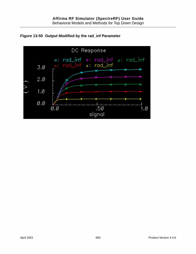
Affirma RF Simulator (SpectreRF) User GuideBehavioral Models and Methods for Top Down Design
Figure 13-50 Output Modified by the rad_inf Parameter
April 2001 650 Product Version 4.4.6
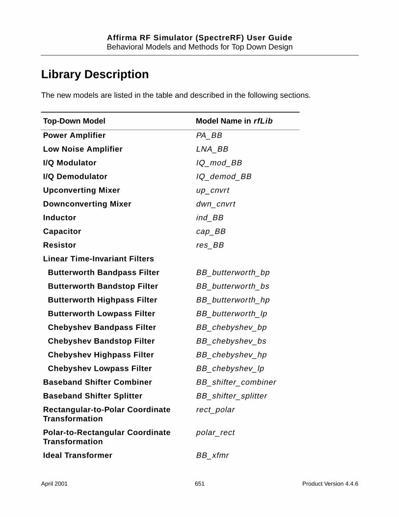
Affirma RF Simulator (SpectreRF) User GuideBehavioral Models and Methods for Top Down Design
Library Description
The new models are listed in the table and described in the following sections.
Top-Down Model Model Name in rfLib
Power Amplifier PA_BB
Low Noise Amplifier LNA_BB
I/Q Modulator IQ_mod_BB
I/Q Demodulator IQ_demod_BB
Upconverting Mixer up_cnvrt
Downconverting Mixer dwn_cnvrt
Inductor ind_BB
Capacitor cap_BB
Resistor res_BB
Linear Time-Invariant Filters
Butterworth Bandpass Filter BB_butterworth_bp
Butterworth Bandstop Filter BB_butterworth_bs
Butterworth Highpass Filter BB_butterworth_hp
Butterworth Lowpass Filter BB_butterworth_lp
Chebyshev Bandpass Filter BB_chebyshev_bp
Chebyshev Bandstop Filter BB_chebyshev_bs
Chebyshev Highpass Filter BB_chebyshev_hp
Chebyshev Lowpass Filter BB_chebyshev_lp
Baseband Shifter Combiner BB_shifter_combiner
Baseband Shifter Splitter BB_shifter_splitter
Rectangular-to-Polar CoordinateTransformation
rect_polar
Polar-to-Rectangular CoordinateTransformation
polar_rect
Ideal Transformer BB_xfmr
April 2001 651 Product Version 4.4.6
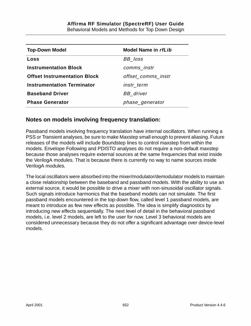
Affirma RF Simulator (SpectreRF) User GuideBehavioral Models and Methods for Top Down Design
Notes on models involving frequency translation:
Passband models involving frequency translation have internal oscillators. When running aPSS or Transient analyses, be sure to make Maxstep small enough to prevent aliasing. Futurereleases of the models will include Boundstep lines to control maxstep from within themodels. Envelope Following and PDISTO analyses do not require a non-default maxstepbecause those analyses require external sources at the same frequencies that exist insidethe VerilogA modules. That is because there is currently no way to name sources insideVerilogA modules.
The local oscillators were absorbed into the mixer/modulator/demodulator models to maintaina close relationship between the baseband and passband models. With the ability to use anexternal source, it would be possible to drive a mixer with non-sinusoidal oscillator signals.Such signals introduce harmonics that the baseband models can not simulate. The firstpassband models encountered in the top-down flow, called level 1 passband models, aremeant to introduce as few new effects as possible. The idea is simplify diagnostics byintroducing new effects sequentially. The next level of detail in the behavioral passbandmodels, i.e. level 2 models, are left to the user for now. Level 3 behavioral models areconsidered unnecessary because they do not offer a significant advantage over device-levelmodels.
Loss BB_loss
Instrumentation Block comms_instr
Offset Instrumentation Block offset_comms_instr
Instrumentation Terminator instr_term
Baseband Driver BB_driver
Phase Generator phase_generator
Top-Down Model Model Name in rfLib
April 2001 652 Product Version 4.4.6
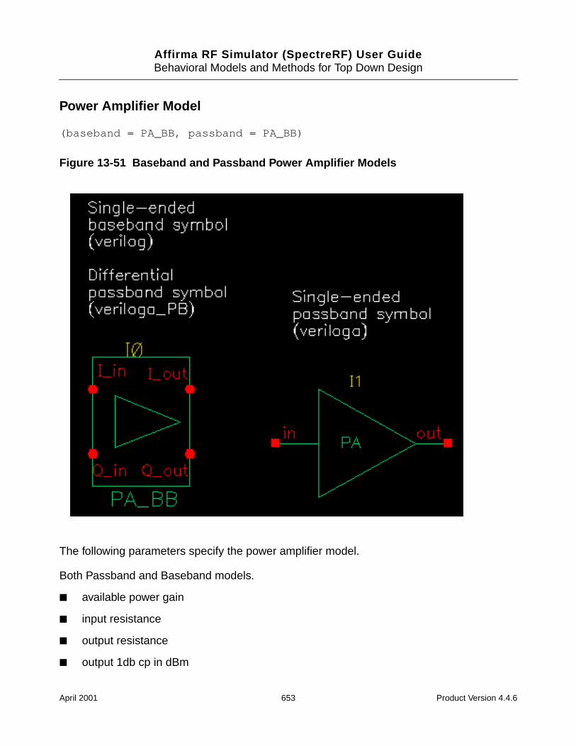
Affirma RF Simulator (SpectreRF) User GuideBehavioral Models and Methods for Top Down Design
Power Amplifier Model
(baseband = PA_BB, passband = PA_BB)
Figure 13-51 Baseband and Passband Power Amplifier Models
The following parameters specify the power amplifier model.
Both Passband and Baseband models.
available power gain
input resistance
output resistance
output 1db cp in dBm
April 2001 653 Product Version 4.4.6

Affirma RF Simulator (SpectreRF) User GuideBehavioral Models and Methods for Top Down Design
noise figure
Baseband model only.
am/pm sharpness
|radians|@1db cp
|radians|@ big input
1,0,-1 for cw,none,ccw
April 2001 654 Product Version 4.4.6
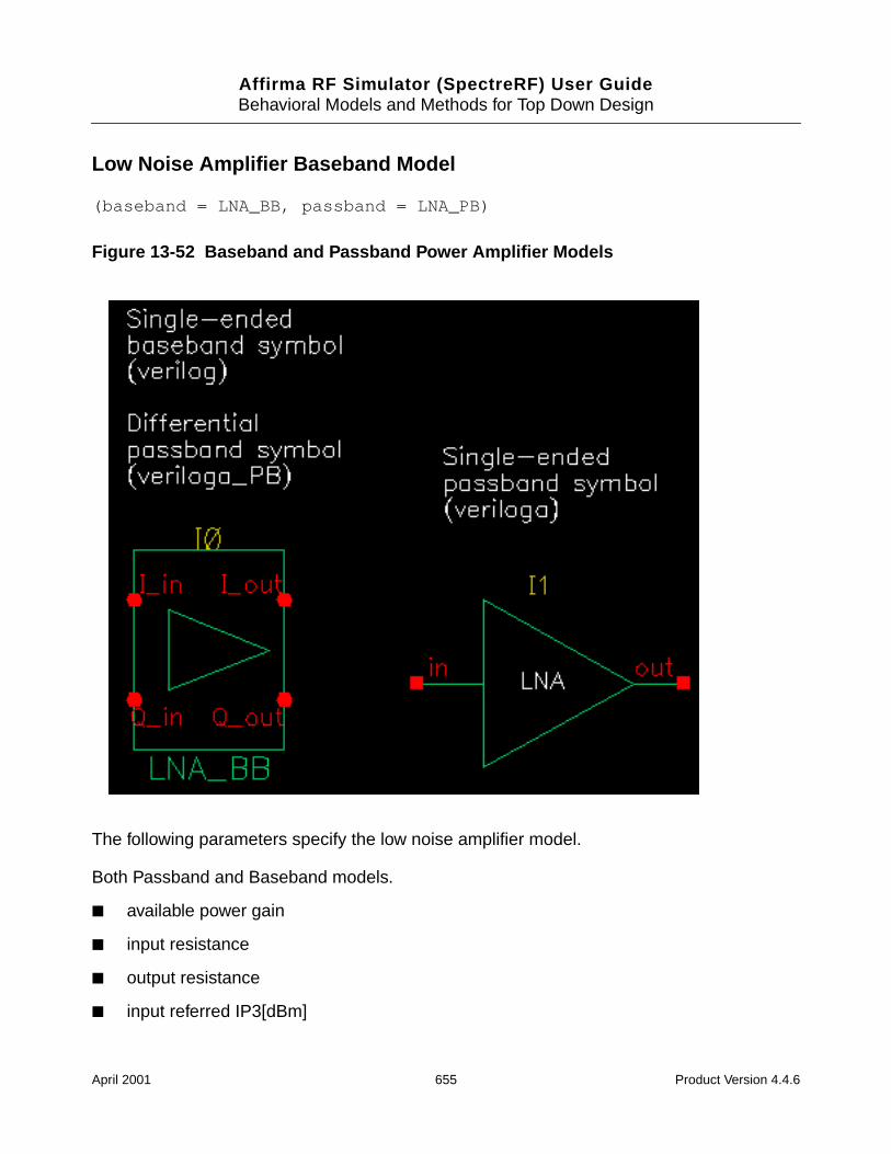
Affirma RF Simulator (SpectreRF) User GuideBehavioral Models and Methods for Top Down Design
Low Noise Amplifier Baseband Model
(baseband = LNA_BB, passband = LNA_PB)
Figure 13-52 Baseband and Passband Power Amplifier Models
The following parameters specify the low noise amplifier model.
Both Passband and Baseband models.
available power gain
input resistance
output resistance
input referred IP3[dBm]
April 2001 655 Product Version 4.4.6
Affirma RF Simulator (SpectreRF) User GuideBehavioral Models and Methods for Top Down Design
noise figure
Baseband model only.
am/pm sharpness
cmp[dBm] = output power level where the next parameter is defined
|radians|@cmp = output phase shift at output power of cmp.
|radians|@ big input
1,0,-1 for cw,none,ccw
April 2001 656 Product Version 4.4.6
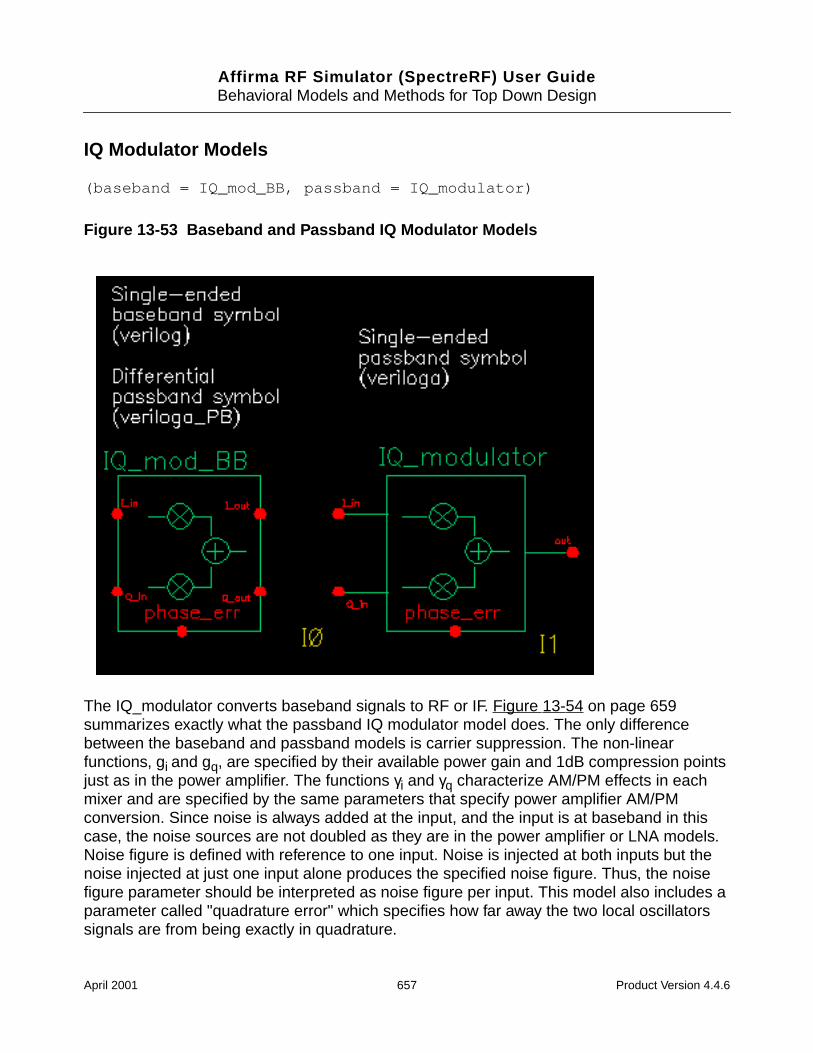
Affirma RF Simulator (SpectreRF) User GuideBehavioral Models and Methods for Top Down Design
IQ Modulator Models
(baseband = IQ_mod_BB, passband = IQ_modulator)
Figure 13-53 Baseband and Passband IQ Modulator Models
The IQ_modulator converts baseband signals to RF or IF. Figure 13-54 on page 659summarizes exactly what the passband IQ modulator model does. The only differencebetween the baseband and passband models is carrier suppression. The non-linearfunctions, gi and gq, are specified by their available power gain and 1dB compression pointsjust as in the power amplifier. The functions γi and γq characterize AM/PM effects in eachmixer and are specified by the same parameters that specify power amplifier AM/PMconversion. Since noise is always added at the input, and the input is at baseband in thiscase, the noise sources are not doubled as they are in the power amplifier or LNA models.Noise figure is defined with reference to one input. Noise is injected at both inputs but thenoise injected at just one input alone produces the specified noise figure. Thus, the noisefigure parameter should be interpreted as noise figure per input. This model also includes aparameter called "quadrature error" which specifies how far away the two local oscillatorssignals are from being exactly in quadrature.
April 2001 657 Product Version 4.4.6
Affirma RF Simulator (SpectreRF) User GuideBehavioral Models and Methods for Top Down Design
"Phase error" is the voltage on the phase error pin. The phase error pin has a fixed noiselessresistive input impedance of 50 ohms. The phase error pin can be used to introduce adynamic phase error or phase noise. Phase noise can be fed into the phase error pin from aphase-domain PLL model or from a Port. Noise in Port models can be specified either by theinternal resistance or by a data file that tabulates a power spectral density. The phase errorpin can also be driven by a ramp or circular integrator output to model a frequency errorbetween the incoming carrier and local oscillator.
The following parameters specify the IQ modulator. The available power gain and one dBcompression point are explained first. The effects of the phase_error pin and the quadratureerror parameter are discussed at the end of this section.
Both Passband and Baseband models.
available I-mixer gain[dB]
available Q-mixer gain[dB]
input resistance
output resistance
I-output 1dB CP[dBm]
Q-output 1dB CP[dBm]
noise figure [dB]
quadrature error
Baseband models only.
I-sharpness factor
Q-sharpness factor
Q-radians@Q_cmp
I-radians@I_cmp
I-radians@big I-input
Q-radians@big-input
1,0,-1 for cw,none,ccw
1,0,-1 for cw,none,ccw
April 2001 658 Product Version 4.4.6
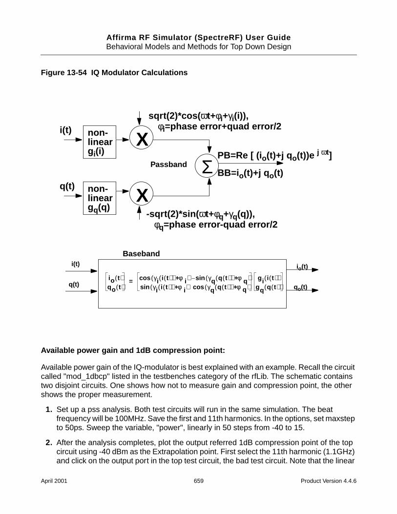
Affirma RF Simulator (SpectreRF) User GuideBehavioral Models and Methods for Top Down Design
Figure 13-54 IQ Modulator Calculations
Available power gain and 1dB compression point:
Available power gain of the IQ-modulator is best explained with an example. Recall the circuitcalled "mod_1dbcp" listed in the testbenches category of the rfLib. The schematic containstwo disjoint circuits. One shows how not to measure gain and compression point, the othershows the proper measurement.
1. Set up a pss analysis. Both test circuits will run in the same simulation. The beatfrequency will be 100MHz. Save the first and 11th harmonics. In the options, set maxstepto 50ps. Sweep the variable, "power", linearly in 50 steps from -40 to 15.
2. After the analysis completes, plot the output referred 1dB compression point of the topcircuit using -40 dBm as the Extrapolation point. First select the 11th harmonic (1.1GHz)and click on the output port in the top test circuit, the bad test circuit. Note that the linear
X
X
Σ
sqrt(2)*cos( ωt+φi+γi(i)),
-sqrt(2)*sin( ωt+φq+γq(q)),
i(t)
q(t)
PB=Re [ (i o(t)+j q o(t))e j ωt]
non-lineargi(i)
non-lineargq(q)
φi=phase error+quad error/2
φq=phase error-quad error/2
io t( )qo t( )
γi i t( )( ) φi+( )cos γq q t( )( ) φq+( )sin–
γi i t( )( ) φi+( )sin γq q t( )( ) φq+( )cosg i i t( )( )
gq q t( )( )=
io(t)
qo(t)
i(t)
q(t)
BB=i o(t)+j q o(t)Passband
Baseband
April 2001 659 Product Version 4.4.6
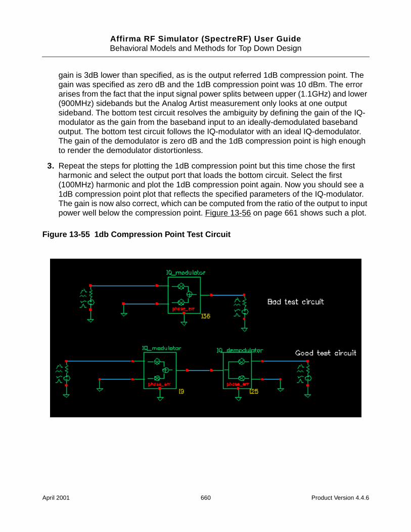
Affirma RF Simulator (SpectreRF) User GuideBehavioral Models and Methods for Top Down Design
gain is 3dB lower than specified, as is the output referred 1dB compression point. Thegain was specified as zero dB and the 1dB compression point was 10 dBm. The errorarises from the fact that the input signal power splits between upper (1.1GHz) and lower(900MHz) sidebands but the Analog Artist measurement only looks at one outputsideband. The bottom test circuit resolves the ambiguity by defining the gain of the IQ-modulator as the gain from the baseband input to an ideally-demodulated basebandoutput. The bottom test circuit follows the IQ-modulator with an ideal IQ-demodulator.The gain of the demodulator is zero dB and the 1dB compression point is high enoughto render the demodulator distortionless.
3. Repeat the steps for plotting the 1dB compression point but this time chose the firstharmonic and select the output port that loads the bottom circuit. Select the first(100MHz) harmonic and plot the 1dB compression point again. Now you should see a1dB compression point plot that reflects the specified parameters of the IQ-modulator.The gain is now also correct, which can be computed from the ratio of the output to inputpower well below the compression point. Figure 13-56 on page 661 shows such a plot.
Figure 13-55 1db Compression Point Test Circuit
April 2001 660 Product Version 4.4.6
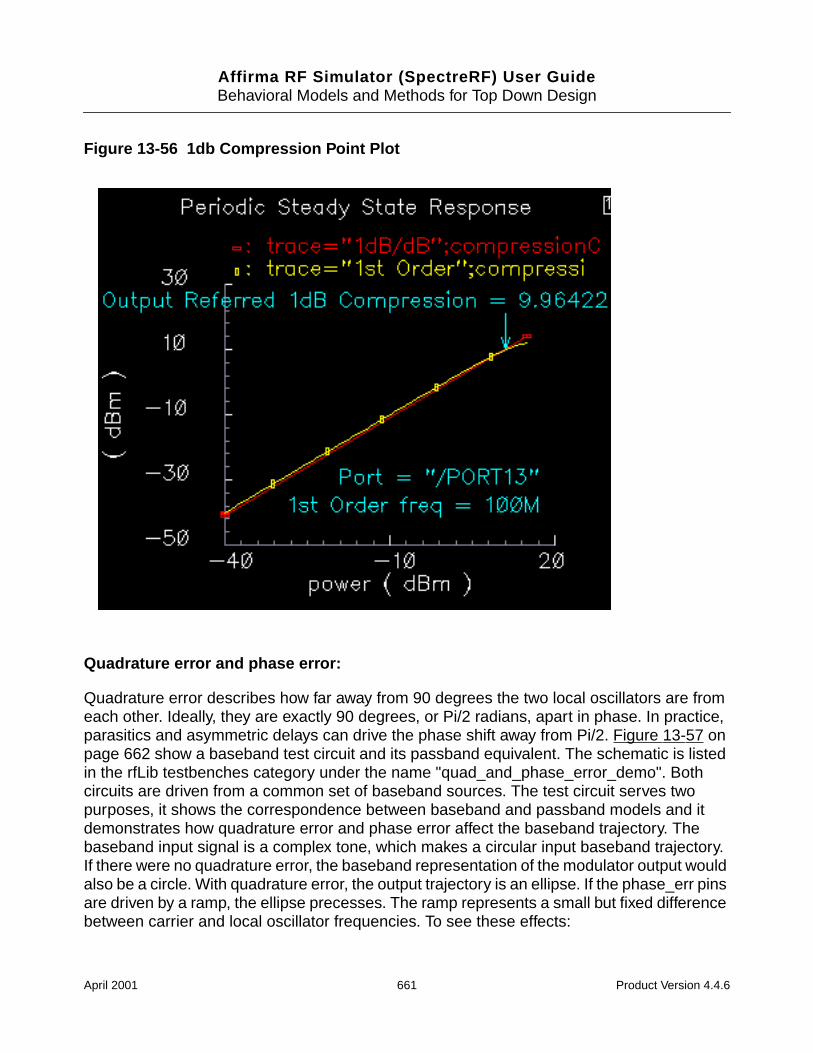
Affirma RF Simulator (SpectreRF) User GuideBehavioral Models and Methods for Top Down Design
Figure 13-56 1db Compression Point Plot
Quadrature error and phase error:
Quadrature error describes how far away from 90 degrees the two local oscillators are fromeach other. Ideally, they are exactly 90 degrees, or Pi/2 radians, apart in phase. In practice,parasitics and asymmetric delays can drive the phase shift away from Pi/2. Figure 13-57 onpage 662 show a baseband test circuit and its passband equivalent. The schematic is listedin the rfLib testbenches category under the name "quad_and_phase_error_demo". Bothcircuits are driven from a common set of baseband sources. The test circuit serves twopurposes, it shows the correspondence between baseband and passband models and itdemonstrates how quadrature error and phase error affect the baseband trajectory. Thebaseband input signal is a complex tone, which makes a circular input baseband trajectory.If there were no quadrature error, the baseband representation of the modulator output wouldalso be a circle. With quadrature error, the output trajectory is an ellipse. If the phase_err pinsare driven by a ramp, the ellipse precesses. The ramp represents a small but fixed differencebetween carrier and local oscillator frequencies. To see these effects:
April 2001 661 Product Version 4.4.6
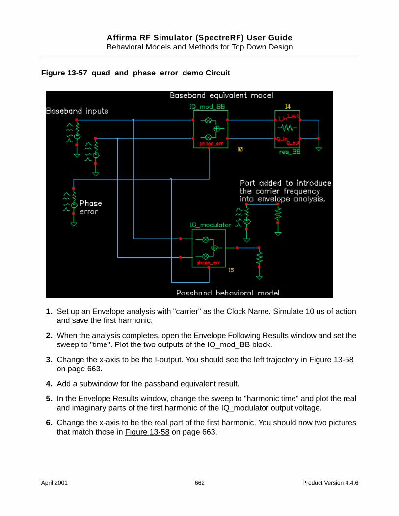
Affirma RF Simulator (SpectreRF) User GuideBehavioral Models and Methods for Top Down Design
Figure 13-57 quad_and_phase_error_demo Circuit
1. Set up an Envelope analysis with "carrier" as the Clock Name. Simulate 10 us of actionand save the first harmonic.
2. When the analysis completes, open the Envelope Following Results window and set thesweep to "time". Plot the two outputs of the IQ_mod_BB block.
3. Change the x-axis to be the I-output. You should see the left trajectory in Figure 13-58on page 663.
4. Add a subwindow for the passband equivalent result.
5. In the Envelope Results window, change the sweep to "harmonic time" and plot the realand imaginary parts of the first harmonic of the IQ_modulator output voltage.
6. Change the x-axis to be the real part of the first harmonic. You should now two picturesthat match those in Figure 13-58 on page 663.
April 2001 662 Product Version 4.4.6
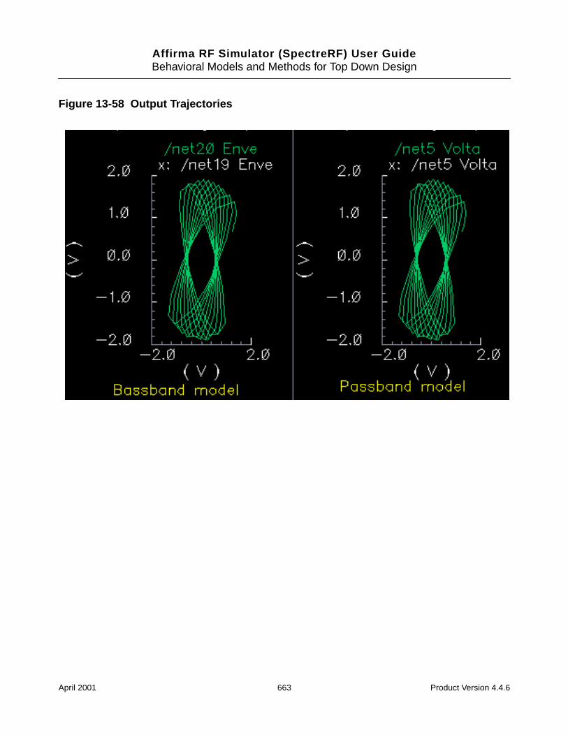
Affirma RF Simulator (SpectreRF) User GuideBehavioral Models and Methods for Top Down Design
Figure 13-58 Output Trajectories
April 2001 663 Product Version 4.4.6
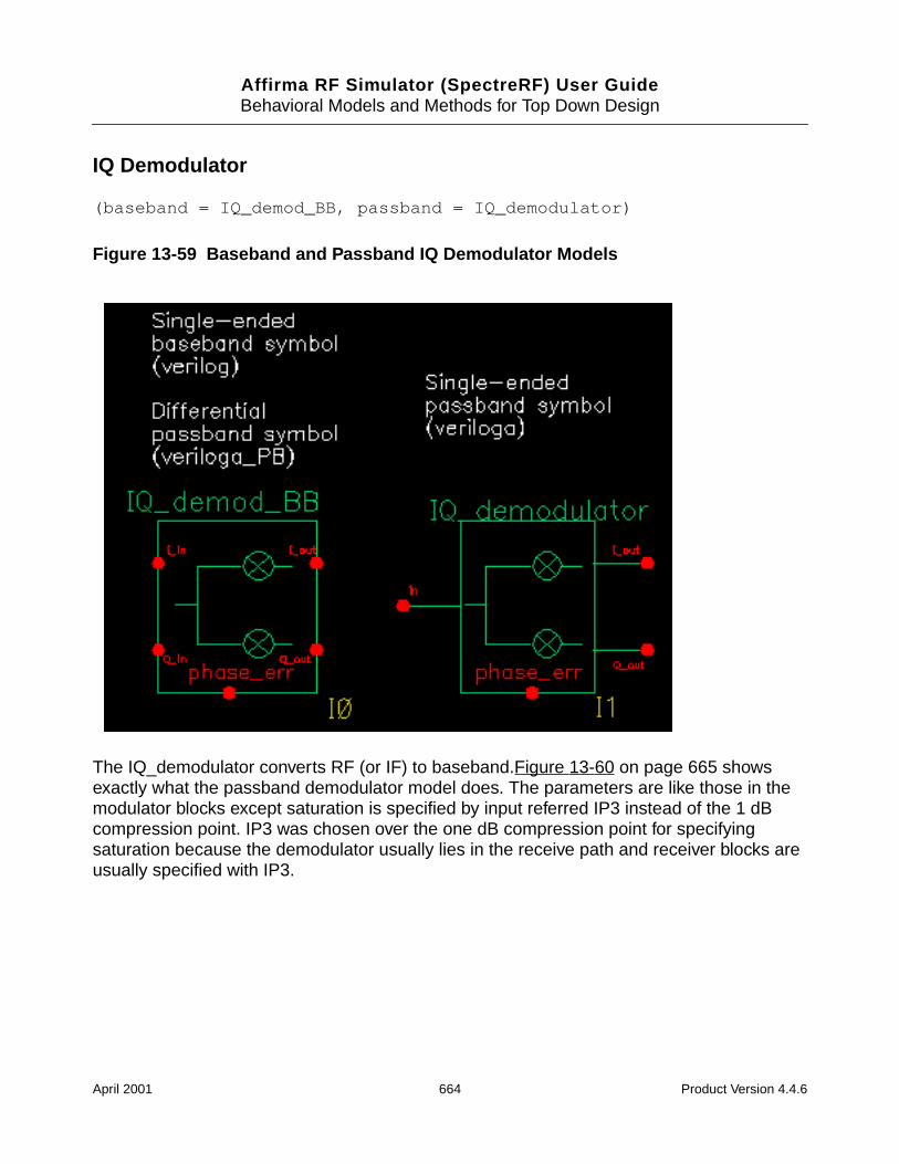
Affirma RF Simulator (SpectreRF) User GuideBehavioral Models and Methods for Top Down Design
IQ Demodulator
(baseband = IQ_demod_BB, passband = IQ_demodulator)
Figure 13-59 Baseband and Passband IQ Demodulator Models
The IQ_demodulator converts RF (or IF) to baseband.Figure 13-60 on page 665 showsexactly what the passband demodulator model does. The parameters are like those in themodulator blocks except saturation is specified by input referred IP3 instead of the 1 dBcompression point. IP3 was chosen over the one dB compression point for specifyingsaturation because the demodulator usually lies in the receive path and receiver blocks areusually specified with IP3.
April 2001 664 Product Version 4.4.6
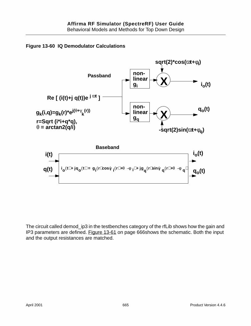
Affirma RF Simulator (SpectreRF) User GuideBehavioral Models and Methods for Top Down Design
Figure 13-60 IQ Demodulator Calculations
The circuit called demod_ip3 in the testbenches category of the rfLib shows how the gain andIP3 parameters are defined. Figure 13-61 on page 666shows the schematic. Both the inputand the output resistances are matched.
X
X
sqrt(2)*cos( ωt+φi)
-sqrt(2)sin( ωt+φq)
io(t)
qo(t)
Re [ (i(t)+j q(t))e j ωt ]
gk(i,q)=g k(r)*ej(θ+γk
(r))
r=Sqrt (i*i+q*q),
non-lineargi
non-lineargq
θ = arctan2(q/i)
io t( ) jq o t( )+ gi r( ) γi r( ) θ φi–+( )cos jgq
r( ) γq r( ) θ φq–+( )sin+=
io(t)
qo(t)
i(t)
q(t)
Baseband
Passband
April 2001 665 Product Version 4.4.6
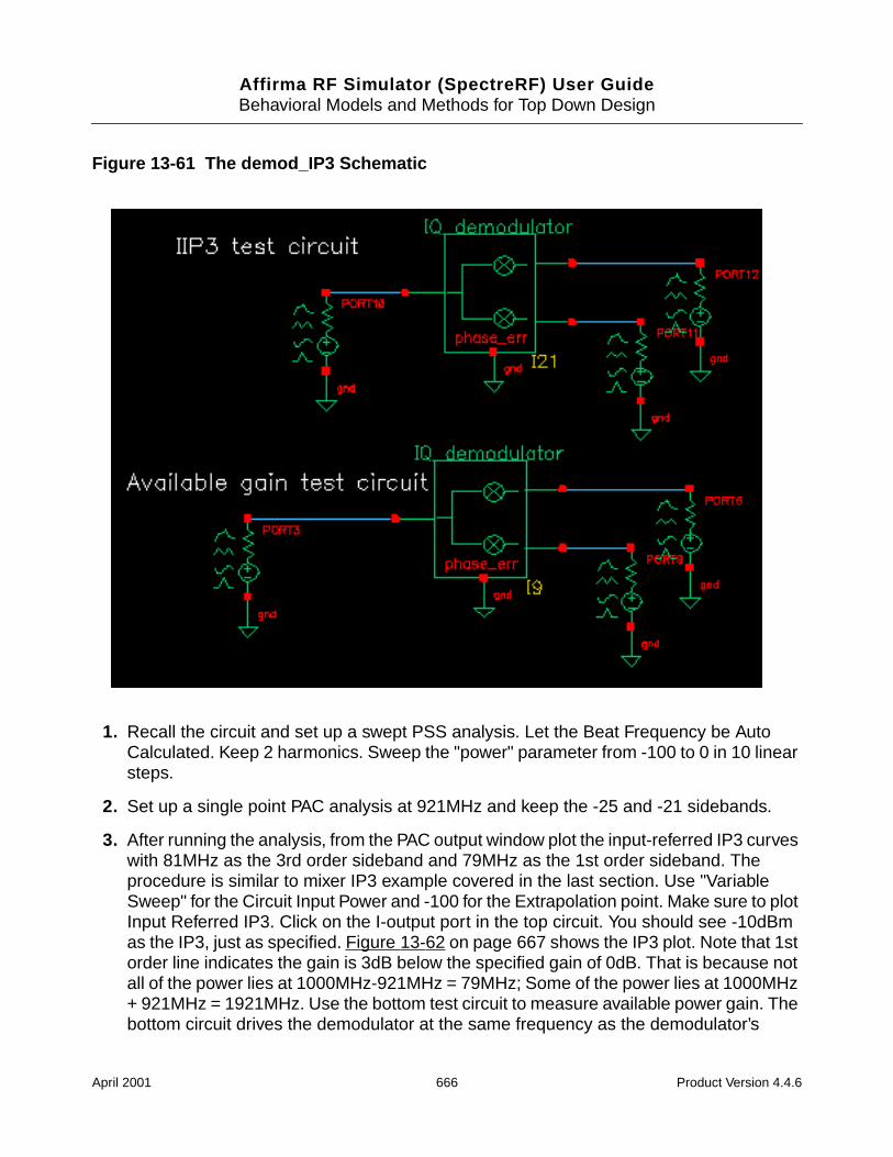
Affirma RF Simulator (SpectreRF) User GuideBehavioral Models and Methods for Top Down Design
Figure 13-61 The demod_IP3 Schematic
1. Recall the circuit and set up a swept PSS analysis. Let the Beat Frequency be AutoCalculated. Keep 2 harmonics. Sweep the "power" parameter from -100 to 0 in 10 linearsteps.
2. Set up a single point PAC analysis at 921MHz and keep the -25 and -21 sidebands.
3. After running the analysis, from the PAC output window plot the input-referred IP3 curveswith 81MHz as the 3rd order sideband and 79MHz as the 1st order sideband. Theprocedure is similar to mixer IP3 example covered in the last section. Use "VariableSweep" for the Circuit Input Power and -100 for the Extrapolation point. Make sure to plotInput Referred IP3. Click on the I-output port in the top circuit. You should see -10dBmas the IP3, just as specified. Figure 13-62 on page 667 shows the IP3 plot. Note that 1storder line indicates the gain is 3dB below the specified gain of 0dB. That is because notall of the power lies at 1000MHz-921MHz = 79MHz; Some of the power lies at 1000MHz+ 921MHz = 1921MHz. Use the bottom test circuit to measure available power gain. Thebottom circuit drives the demodulator at the same frequency as the demodulator’s
April 2001 666 Product Version 4.4.6
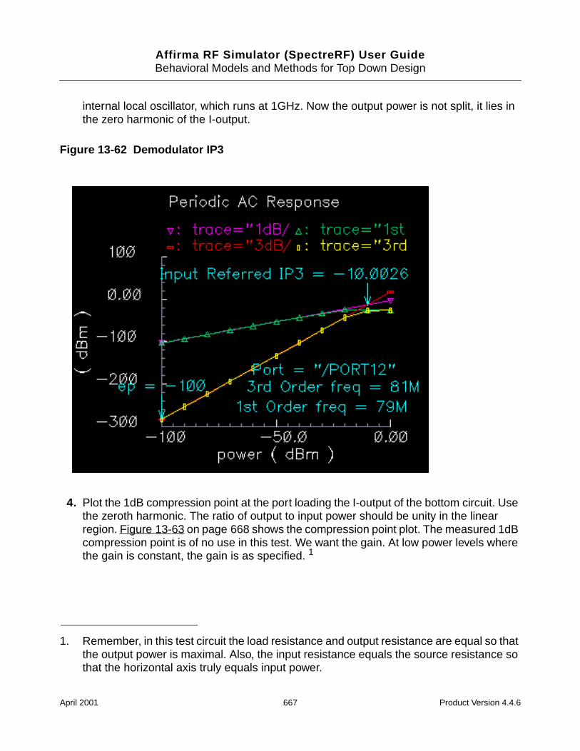
Affirma RF Simulator (SpectreRF) User GuideBehavioral Models and Methods for Top Down Design
internal local oscillator, which runs at 1GHz. Now the output power is not split, it lies inthe zero harmonic of the I-output.
Figure 13-62 Demodulator IP3
4. Plot the 1dB compression point at the port loading the I-output of the bottom circuit. Usethe zeroth harmonic. The ratio of output to input power should be unity in the linearregion. Figure 13-63 on page 668 shows the compression point plot. The measured 1dBcompression point is of no use in this test. We want the gain. At low power levels wherethe gain is constant, the gain is as specified. 1
1. Remember, in this test circuit the load resistance and output resistance are equal so thatthe output power is maximal. Also, the input resistance equals the source resistance sothat the horizontal axis truly equals input power.
April 2001 667 Product Version 4.4.6
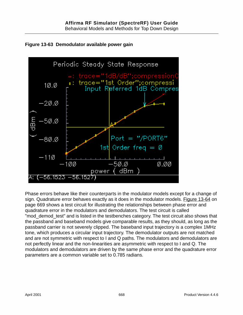
Affirma RF Simulator (SpectreRF) User GuideBehavioral Models and Methods for Top Down Design
Figure 13-63 Demodulator available power gain
Phase errors behave like their counterparts in the modulator models except for a change ofsign. Quadrature error behaves exactly as it does in the modulator models. Figure 13-64 onpage 669 shows a test circuit for illustrating the relationships between phase error andquadrature error in the modulators and demodulators. The test circuit is called"mod_demod_test" and is listed in the testbenches category. The test circuit also shows thatthe passband and baseband models give comparable results, as they should, as long as thepassband carrier is not severely clipped. The baseband input trajectory is a complex 1MHztone, which produces a circular input trajectory. The demodulator outputs are not matchedand are not symmetric with respect to I and Q paths. The modulators and demodulators arenot perfectly linear and the non-linearities are asymmetric with respect to I and Q. Themodulators and demodulators are driven by the same phase error and the quadrature errorparameters are a common variable set to 0.785 radians.
April 2001 668 Product Version 4.4.6
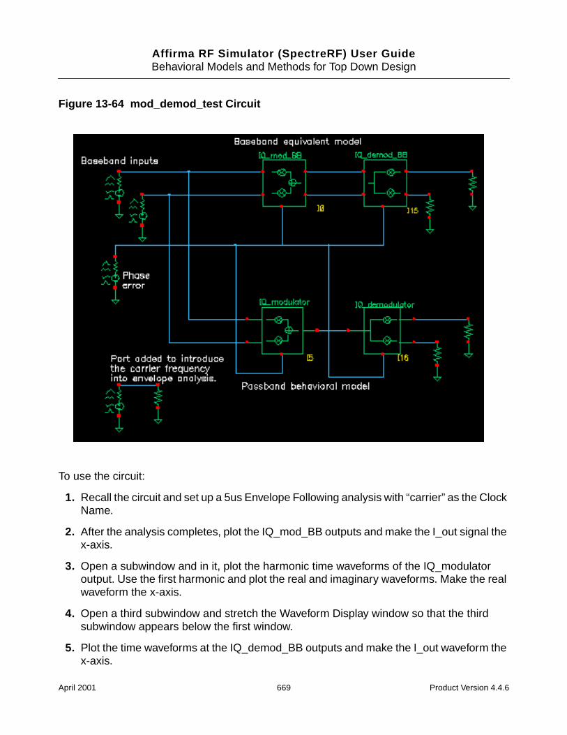
Affirma RF Simulator (SpectreRF) User GuideBehavioral Models and Methods for Top Down Design
Figure 13-64 mod_demod_test Circuit
To use the circuit:
1. Recall the circuit and set up a 5us Envelope Following analysis with “carrier” as the ClockName.
2. After the analysis completes, plot the IQ_mod_BB outputs and make the I_out signal thex-axis.
3. Open a subwindow and in it, plot the harmonic time waveforms of the IQ_modulatoroutput. Use the first harmonic and plot the real and imaginary waveforms. Make the realwaveform the x-axis.
4. Open a third subwindow and stretch the Waveform Display window so that the thirdsubwindow appears below the first window.
5. Plot the time waveforms at the IQ_demod_BB outputs and make the I_out waveform thex-axis.
April 2001 669 Product Version 4.4.6

Affirma RF Simulator (SpectreRF) User GuideBehavioral Models and Methods for Top Down Design
6. Open a fourth subwindow and plot the harmonic time results at the IQ_demodulatoroutputs but this time use the zeroth harmonic and only plot the real parts. Make the I_outwaveform the x-axis. Figure 13-65 on page 671 shows what you should now see.
The leftmost pictures are from the baseband models and the rightmost are from the passbandmodels. Passband and baseband models agree quite well. The top pictures are the voltagesat nodes that lie between the modulator and demodulator. Quadrature error squashes thebaseband trajectory at that node. The trajectory precesses because phase error ramps uplinearly with time just like in the last test. The non-linearities produce the sharp corners. Thebottom trajectories do not precess because the same phase error rotates the demodulatoroutput in the reverse direction; driven by the same phase error ramp, the demodulator undoesthe precession introduced in the modulator. The demodulator outputs are nearly in phasebecause the quadrature errors of pi/4 in the modulators and demodulators add to give a totalquadrature error of Pi/2, which in this case puts the baseband I and Q outputs nearly in phasewith each other.
April 2001 670 Product Version 4.4.6
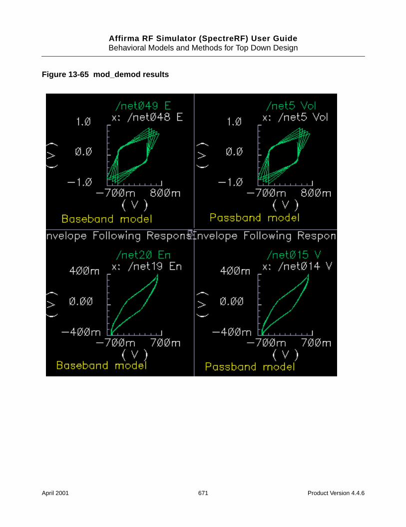
Affirma RF Simulator (SpectreRF) User GuideBehavioral Models and Methods for Top Down Design
Figure 13-65 mod_demod results
April 2001 671 Product Version 4.4.6
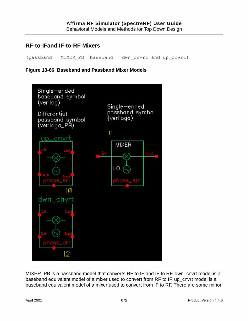
Affirma RF Simulator (SpectreRF) User GuideBehavioral Models and Methods for Top Down Design
RF-to-IFand IF-to-RF Mixers
(passband = MIXER_PB, baseband = dwn_cnvrt and up_cnvrt)
Figure 13-66 Baseband and Passband Mixer Models
MIXER_PB is a passband model that converts RF to IF and IF to RF. dwn_cnvrt model is abaseband equivalent model of a mixer used to convert from RF to IF. up_cnvrt model is abaseband equivalent model of a mixer used to convert from IF to RF. There are some minor
April 2001 672 Product Version 4.4.6
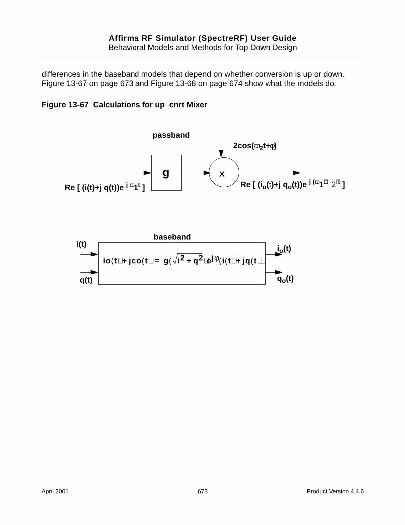
Affirma RF Simulator (SpectreRF) User GuideBehavioral Models and Methods for Top Down Design
differences in the baseband models that depend on whether conversion is up or down.Figure 13-67 on page 673 and Figure 13-68 on page 674 show what the models do.
Figure 13-67 Calculations for up_cnrt Mixer
X
2cos( ω2t+φ)
Re [ (i(t)+j q(t))e j ω1t ] Re [ (i o(t)+j q o(t))e j (ω1+ω2)t ]
io t( ) jqo t( )+ g i 2 q2+( )ejφ i t( ) jq t( )+( )=
i(t)
q(t)
io(t)
qo(t)
baseband
g
passband
April 2001 673 Product Version 4.4.6
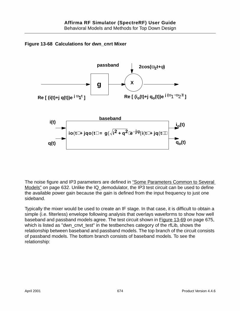
Affirma RF Simulator (SpectreRF) User GuideBehavioral Models and Methods for Top Down Design
Figure 13-68 Calculations for dwn_cnrt Mixer
The noise figure and IP3 parameters are defined in “Some Parameters Common to SeveralModels” on page 632. Unlike the IQ_demodulator, the IP3 test circuit can be used to definethe available power gain because the gain is defined from the input frequency to just onesideband.
Typically the mixer would be used to create an IF stage. In that case, it is difficult to obtain asimple (i.e. filterless) envelope following analysis that overlays waveforms to show how wellbaseband and passband models agree. The test circuit shown in Figure 13-69 on page 675,which is listed as "dwn_cnvt_test" in the testbenches category of the rfLib, shows therelationship between baseband and passband models. The top branch of the circuit consistsof passband models. The bottom branch consists of baseband models. To see therelationship:
X
2cos( ω2t+φ)
Re [ (i(t)+j q(t))e j ω1t ] Re [ (i o(t)+j q o(t))e j (ω1−ω2)t ]
g
io t( ) jqo t( )+ g i 2 q2+( )e j– φ i t( ) jq t( )+( )=
i(t)
q(t)
io(t)
qo(t)
baseband
passband
April 2001 674 Product Version 4.4.6
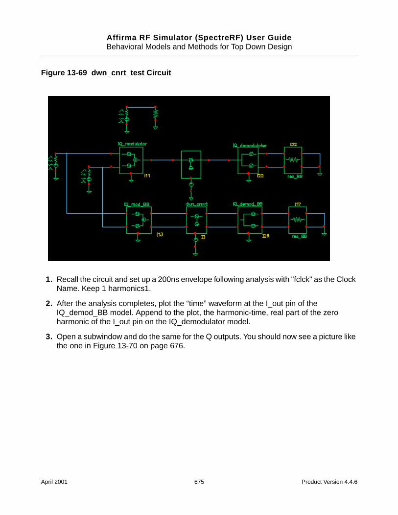
Affirma RF Simulator (SpectreRF) User GuideBehavioral Models and Methods for Top Down Design
Figure 13-69 dwn_cnrt_test Circuit
1. Recall the circuit and set up a 200ns envelope following analysis with "fclck" as the ClockName. Keep 1 harmonics1.
2. After the analysis completes, plot the “time” waveform at the I_out pin of theIQ_demod_BB model. Append to the plot, the harmonic-time, real part of the zeroharmonic of the I_out pin on the IQ_demodulator model.
3. Open a subwindow and do the same for the Q outputs. You should now see a picture likethe one in Figure 13-70 on page 676.
April 2001 675 Product Version 4.4.6
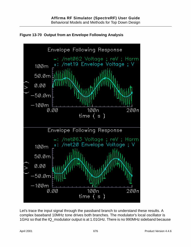
Affirma RF Simulator (SpectreRF) User GuideBehavioral Models and Methods for Top Down Design
Figure 13-70 Output from an Envelope Following Analysis
Let’s trace the input signal through the passband branch to understand these results. Acomplex baseband 10MHz tone drives both branches. The modulator’s local oscillator is1GHz so that the IQ_modulator output is at 1.01GHz. There is no 990MHz sideband because
April 2001 676 Product Version 4.4.6
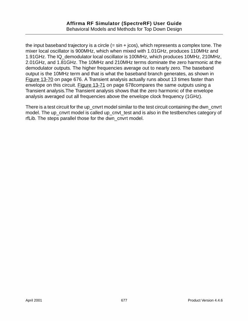
Affirma RF Simulator (SpectreRF) User GuideBehavioral Models and Methods for Top Down Design
the input baseband trajectory is a circle (= sin + jcos), which represents a complex tone. Themixer local oscillator is 900MHz, which when mixed with 1.01GHz, produces 110MHz and1.91GHz. The IQ_demodulator local oscillator is 100MHz, which produces 10MHz, 210MHz,2.01GHz, and 1.81GHz. The 10MHz and 210MHz terms dominate the zero harmonic at thedemodulator outputs. The higher frequencies average out to nearly zero. The basebandoutput is the 10MHz term and that is what the baseband branch generates, as shown inFigure 13-70 on page 676. A Transient analysis actually runs about 13 times faster thanenvelope on this circuit. Figure 13-71 on page 678compares the same outputs using aTransient analysis.The Transient analysis shows that the zero harmonic of the envelopeanalysis averaged out all frequencies above the envelope clock frequency (1GHz).
There is a test circuit for the up_cnvrt model similar to the test circuit containing the dwn_cnvrtmodel. The up_cnvrt model is called up_cnvt_test and is also in the testbenches category ofrfLib. The steps parallel those for the dwn_cnvrt model.
April 2001 677 Product Version 4.4.6
Affirma RF Simulator (SpectreRF) User GuideBehavioral Models and Methods for Top Down Design
Figure 13-71 Results from a Transient Analysis
April 2001 678 Product Version 4.4.6
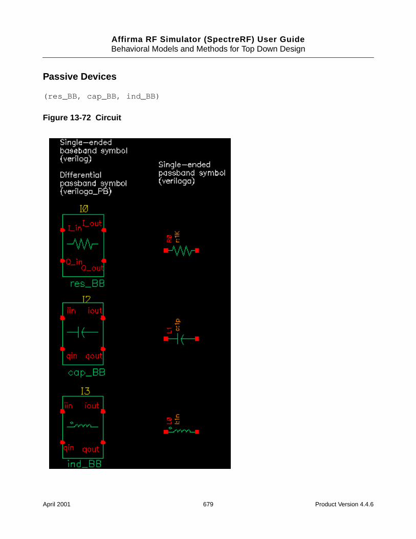
Affirma RF Simulator (SpectreRF) User GuideBehavioral Models and Methods for Top Down Design
Passive Devices
(res_BB, cap_BB, ind_BB)
Figure 13-72 Circuit
April 2001 679 Product Version 4.4.6
Affirma RF Simulator (SpectreRF) User GuideBehavioral Models and Methods for Top Down Design
Resistors
Besides the resistance, the baseband resistor model has a parameter for turning its thermalnoise on or off. The baseband resistor is intended for use at a passband node because it’snoise is doubled. (This was discussed in the section entitled “Relationship between basebandand passband noise”). Figure 13-73 on page 680 shows the symbol, baseband, andpassband models. The total noise in the differential passband resistor model equals the noisein one resistor of R Ohms.
Figure 13-73 Resistor model
Inductors
The library overview described the basic idea behind baseband modeling of inductors. Thebaseband inductor model requires one additional parameter besides the inductance, thecarrier frequency. Figure 13-74 on page 681 shows equivalent schematics of the basebandand differential passband inductor models. The inductor models are noiseless.
April 2001 680 Product Version 4.4.6
Affirma RF Simulator (SpectreRF) User GuideBehavioral Models and Methods for Top Down Design
Figure 13-74 Inductor model
Capacitors
The capacitor is the mathematical dual of the inductor. Figure 13-75 on page 682 shows thebaseband and differential passband capacitor models.
April 2001 681 Product Version 4.4.6
Affirma RF Simulator (SpectreRF) User GuideBehavioral Models and Methods for Top Down Design
Figure 13-75 Capacitor model
April 2001 682 Product Version 4.4.6
Affirma RF Simulator (SpectreRF) User GuideBehavioral Models and Methods for Top Down Design
RLC test circuits
The two circuits discussed below demonstrate how passband and baseband reactiveelements are related. The circuit in Figure 13-76 on page 683 shows a simple passband RLCcircuit driven by a modulated carrier. The circuit in Figure 13-77 on page 684 shows theassociated baseband equivalent circuit model. The circuits are "PB_ind_cap_test" and"BB_ind_cap_test". Both circuits reside in the rfLib under the testbenches category.
Figure 13-76 Simple Passband RLC Circuit
April 2001 683 Product Version 4.4.6
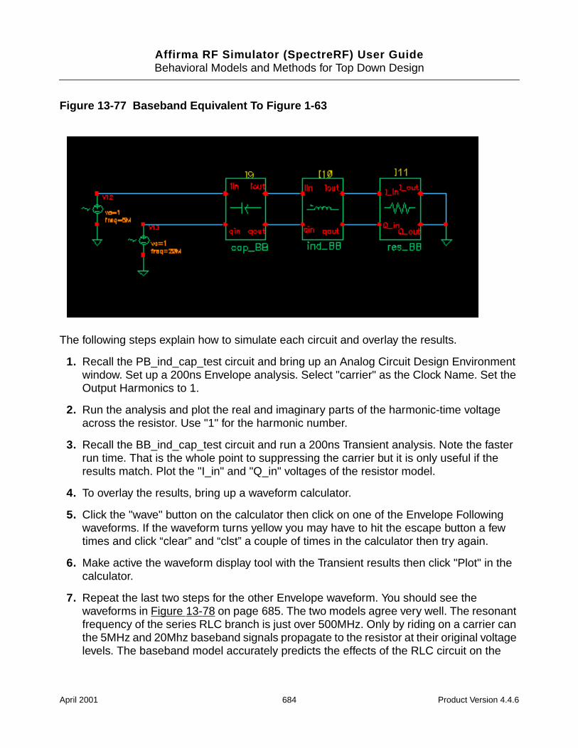
Affirma RF Simulator (SpectreRF) User GuideBehavioral Models and Methods for Top Down Design
Figure 13-77 Baseband Equivalent To Figure 1-63
The following steps explain how to simulate each circuit and overlay the results.
1. Recall the PB_ind_cap_test circuit and bring up an Analog Circuit Design Environmentwindow. Set up a 200ns Envelope analysis. Select "carrier" as the Clock Name. Set theOutput Harmonics to 1.
2. Run the analysis and plot the real and imaginary parts of the harmonic-time voltageacross the resistor. Use "1" for the harmonic number.
3. Recall the BB_ind_cap_test circuit and run a 200ns Transient analysis. Note the fasterrun time. That is the whole point to suppressing the carrier but it is only useful if theresults match. Plot the "I_in" and "Q_in" voltages of the resistor model.
4. To overlay the results, bring up a waveform calculator.
5. Click the "wave" button on the calculator then click on one of the Envelope Followingwaveforms. If the waveform turns yellow you may have to hit the escape button a fewtimes and click “clear” and “clst” a couple of times in the calculator then try again.
6. Make active the waveform display tool with the Transient results then click "Plot" in thecalculator.
7. Repeat the last two steps for the other Envelope waveform. You should see thewaveforms in Figure 13-78 on page 685. The two models agree very well. The resonantfrequency of the series RLC branch is just over 500MHz. Only by riding on a carrier canthe 5MHz and 20Mhz baseband signals propagate to the resistor at their original voltagelevels. The baseband model accurately predicts the effects of the RLC circuit on the
April 2001 684 Product Version 4.4.6
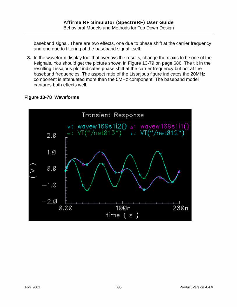
Affirma RF Simulator (SpectreRF) User GuideBehavioral Models and Methods for Top Down Design
baseband signal. There are two effects, one due to phase shift at the carrier frequencyand one due to filtering of the baseband signal itself.
8. In the waveform display tool that overlays the results, change the x-axis to be one of theI-signals. You should get the picture shown in Figure 13-79 on page 686. The tilt in theresulting Lissajous plot indicates phase shift at the carrier frequency but not at thebaseband frequencies. The aspect ratio of the Lissajous figure indicates the 20MHzcomponent is attenuated more than the 5MHz component. The baseband modelcaptures both effects well.
Figure 13-78 Waveforms
April 2001 685 Product Version 4.4.6
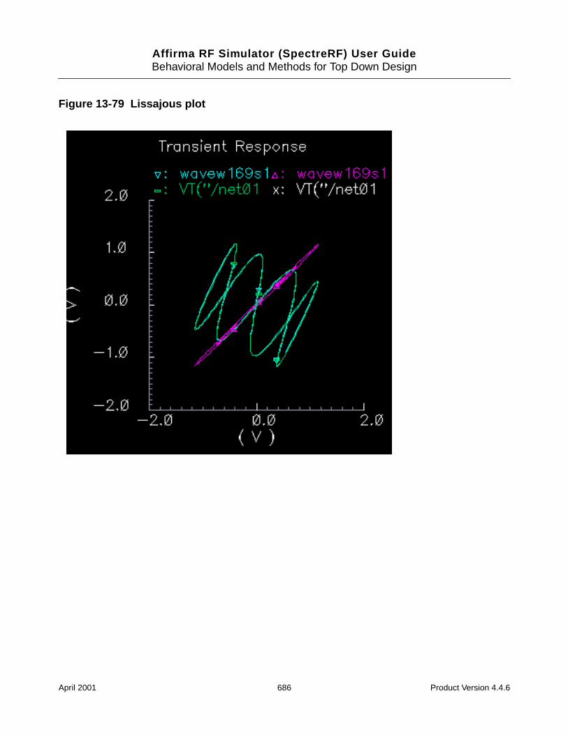
Affirma RF Simulator (SpectreRF) User GuideBehavioral Models and Methods for Top Down Design
Figure 13-79 Lissajous plot
April 2001 686 Product Version 4.4.6
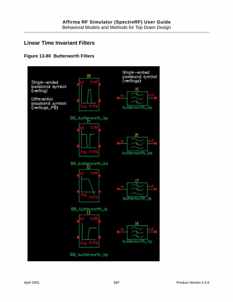
Affirma RF Simulator (SpectreRF) User GuideBehavioral Models and Methods for Top Down Design
Linear Time Invariant Filters
Figure 13-80 Butterworth Filters
April 2001 687 Product Version 4.4.6
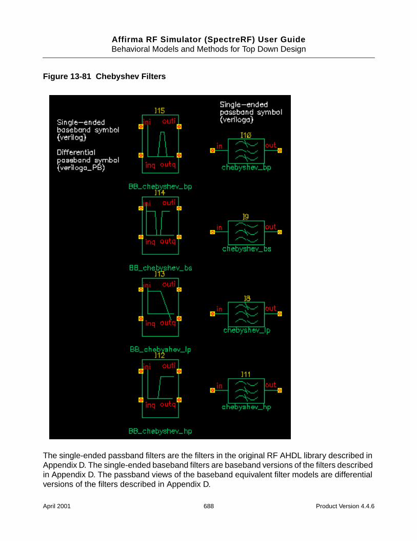
Affirma RF Simulator (SpectreRF) User GuideBehavioral Models and Methods for Top Down Design
Figure 13-81 Chebyshev Filters
The single-ended passband filters are the filters in the original RF AHDL library described inAppendix D. The single-ended baseband filters are baseband versions of the filters describedin Appendix D. The passband views of the baseband equivalent filter models are differentialversions of the filters described in Appendix D.
April 2001 688 Product Version 4.4.6
Affirma RF Simulator (SpectreRF) User GuideBehavioral Models and Methods for Top Down Design
All filter models are LC ladder networks built up during the netlisting step. The only differencebetween the single-ended passband and baseband models is that the baseband models usebaseband equivalent inductor and capacitor models, which means the baseband filter modelshave twice as many nodes as their passband counterparts. The only difference in theparameter list is that the baseband models require the carrier frequency. The carrierfrequency is independent of all other parameters. It is the frequency at which the basebandsignal is reference. If the input signal rides on a carrier that is offset from the reference carrier,the input baseband signal should be spun at the offset frequency before entering the filtermodel. This can be done at the preceding mixer stage by ramping the phase_err pin at a rateequal to the frequency offset.
Parameters (All parameters are defined in terms of passband models.)
Note: The input impedance must be less than or equal to the output impedance to producethe desired filter response.
Input and Output impedance:
The input and output impedances are resistive reference impedances used to compute theinductors and capacitors that make up the filter. The input and output impedances are notterminal impedances. If you load one side of a filter from the library with a resistor of R Ohmsand drive the other side with a frequency-swept current source of 1 Amp, you will see avoltage of R Volts across the current source at the passband frequency. (If the filter is abandstop filter the passband is on either side of the stop band.) The following stepsdemonstrate this point with the four Butterworth filters.
1. Bring up a new schematic in any library to which you can write.
2. Instantiate a butterworth_bp (bandpass) filter with the parameters as shown in
April 2001 689 Product Version 4.4.6
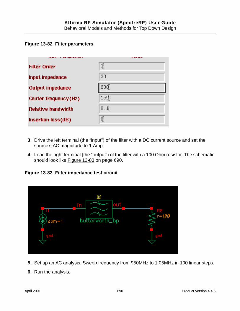
Affirma RF Simulator (SpectreRF) User GuideBehavioral Models and Methods for Top Down Design
Figure 13-82 Filter parameters
3. Drive the left terminal (the “input”) of the filter with a DC current source and set thesource’s AC magnitude to 1 Amp.
4. Load the right terminal (the “output”) of the filter with a 100 Ohm resistor. The schematicshould look like Figure 13-83 on page 690.
Figure 13-83 Filter impedance test circuit
5. Set up an AC analysis. Sweep frequency from 950MHz to 1.05MHz in 100 linear steps.
6. Run the analysis.
April 2001 690 Product Version 4.4.6
Affirma RF Simulator (SpectreRF) User GuideBehavioral Models and Methods for Top Down Design
7. Plot the voltage across the current source. You should see the voltage across the currentsource dip to 100 Volts right at the center frequency of 1GHz. At the center frequency,the impedance looking into a bandpass filter equals the impedance loading the otherside, regardless of the filter’s input and output impedance parameters.
8. Change the filter to butterworth_bs (bandstop filter).
9. Check and save the schematic.
10. In the AC analysis setup, change the AC analysis to sweep frequency from 1Hz to100GHz in 1 linear step. Do not add any specific points.
11. Run the analysis.
12. Plot the voltage across the current source. You should see 100 Volts at either end pointof the sweep. Far away from the center frequency of a bandstop filter, the impedancelooking into the filter equals the impedance loading the other side.
13. Change the filter to butterworth_lp (low pass filter). Set the corner frequency to 10MHz.
14. Check and save the schematic.
15. Change the AC analysis to sweep from 1Hz to 1GHz logarithmically with 10 points perdecade.
16. Run the analysis.
17. Plot the voltage across the current source. Near DC, the impedance looking into a lowpass filter equals the impedance loading the other side.
18. Change the filter to butterworth_hp (highpass filter).
19. Change the AC analysis to sweep from 1GHz to 100GHz.
20. Run the Analysis.
21. Plot the voltage across the current source. As frequency goes to infinity, the impedancelooking into a highpass filter equals the impedance loading the other side.
How are the input and output impedances used if they don’t determine terminalimpedances? Let the filter be specified with input and output resistances of rin and routrespectively. If you drive the filter with a Port of rin Ohms and load it with a Port of rout Ohms,an S-parameter analysis will produce an S21 with the shape associated with the filter typeand associated specifications. The following steps demonstrate this point.
1. Bring up a new schematic window in a library you can write to.
2. Instantiate a butterworth_lp (low pass filter) and set the parameters as shown inFigure 13-84 on page 692.
April 2001 691 Product Version 4.4.6
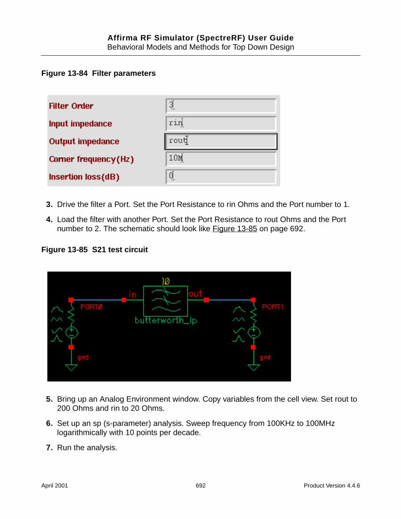
Affirma RF Simulator (SpectreRF) User GuideBehavioral Models and Methods for Top Down Design
Figure 13-84 Filter parameters
3. Drive the filter a Port. Set the Port Resistance to rin Ohms and the Port number to 1.
4. Load the filter with another Port. Set the Port Resistance to rout Ohms and the Portnumber to 2. The schematic should look like Figure 13-85 on page 692.
Figure 13-85 S21 test circuit
5. Bring up an Analog Environment window. Copy variables from the cell view. Set rout to200 Ohms and rin to 20 Ohms.
6. Set up an sp (s-parameter) analysis. Sweep frequency from 100KHz to 100MHzlogarithmically with 10 points per decade.
7. Run the analysis.
April 2001 692 Product Version 4.4.6
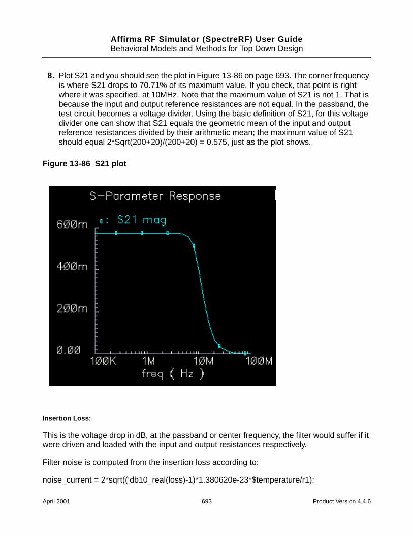
Affirma RF Simulator (SpectreRF) User GuideBehavioral Models and Methods for Top Down Design
8. Plot S21 and you should see the plot in Figure 13-86 on page 693. The corner frequencyis where S21 drops to 70.71% of its maximum value. If you check, that point is rightwhere it was specified, at 10MHz. Note that the maximum value of S21 is not 1. That isbecause the input and output reference resistances are not equal. In the passband, thetest circuit becomes a voltage divider. Using the basic definition of S21, for this voltagedivider one can show that S21 equals the geometric mean of the input and outputreference resistances divided by their arithmetic mean; the maximum value of S21should equal 2*Sqrt(200+20)/(200+20) = 0.575, just as the plot shows.
Figure 13-86 S21 plot
Insertion Loss:
This is the voltage drop in dB, at the passband or center frequency, the filter would suffer if itwere driven and loaded with the input and output resistances respectively.
Filter noise is computed from the insertion loss according to:
noise_current = 2*sqrt((‘db10_real(loss)-1)*1.380620e-23*$temperature/r1);
April 2001 693 Product Version 4.4.6
Affirma RF Simulator (SpectreRF) User GuideBehavioral Models and Methods for Top Down Design
“r1” is the input impedance and “db10_real()” is a function that maps loss in dB into linearattenuation. The definition is as follows:
‘define db10_real(x) (pow(10, (x)/10))
Filter Order:
Low pass-This is total number of reactive elements in the filter. If the order is odd, there is onemore capacitor than inductors. If the order is even, there are equal numbers of capacitors andinductors.
High pass-This is the total number of reactive elements in the filter. If the order is odd, thereis one more inductor than capacitors. If the order if even there are equal numbers ofcapacitors and inductors.
Band pass and Band stop- The filter order is the number of inductor/capacitor pairs.
Corner frequency:
This is the frequency where S21 is 3dB below the peak response when driven and loadedwith the input and output resistances respectively.
Center frequency:
For bandpass filters, the center frequency is where S21 is maximum. For bandstop filters, thecenter frequency is where S21 is a minimum.
Relative bandwidth:
This applies to band pass and band stop filters. It is the normalized frequency differencebetween points straddling the center frequency that correspond a 3dB drop (or rise) from thepeak (dip) of S21. The normalization factor is the center frequency. In other words, the relativebandwidth is specified in terms of a fraction of the center frequency. A relative bandwidth of0.1 and a carrier frequency of 1GHz means that in the case of a bandpass filter, the passband goes from 950MHz to 1.05GHz with the band edges defined by those points lying 3dBbelow the peak response.
Passband ripple:
This applies only to Chebyshev filters. It is the peak-to-peak variation of the transfer functionin the passband when the filter is driven and loaded with the input and output resistances.
April 2001 694 Product Version 4.4.6
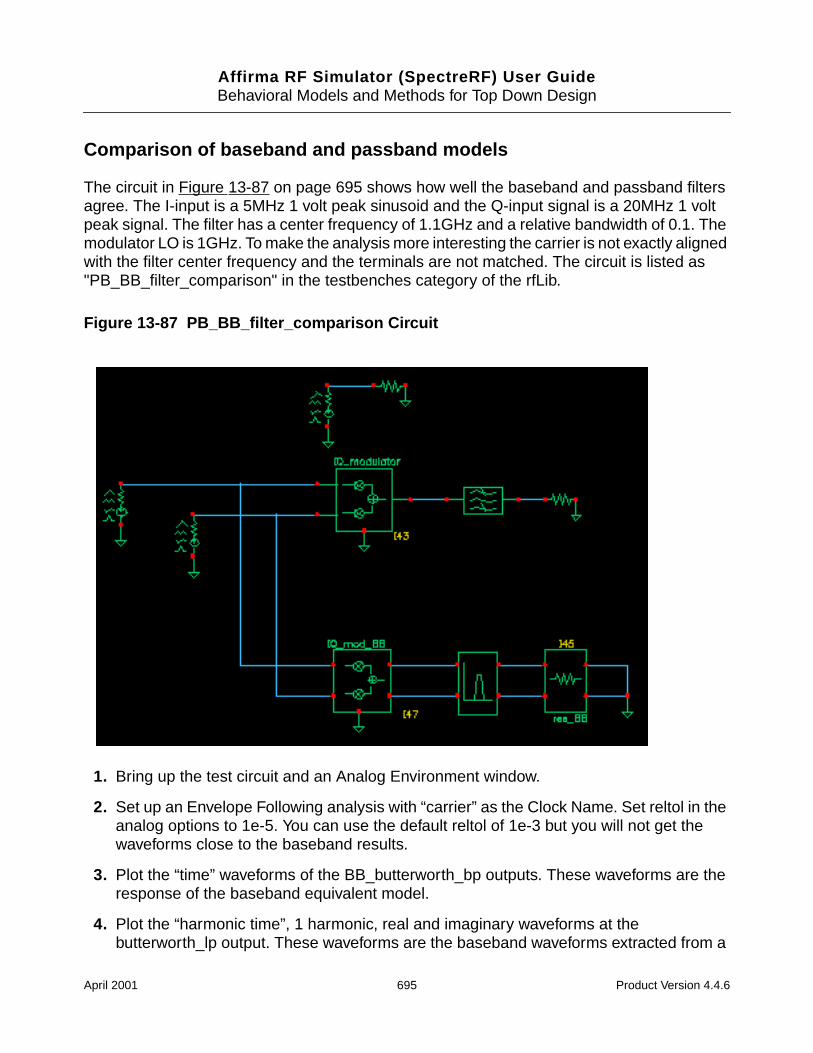
Affirma RF Simulator (SpectreRF) User GuideBehavioral Models and Methods for Top Down Design
Comparison of baseband and passband models
The circuit in Figure 13-87 on page 695 shows how well the baseband and passband filtersagree. The I-input is a 5MHz 1 volt peak sinusoid and the Q-input signal is a 20MHz 1 voltpeak signal. The filter has a center frequency of 1.1GHz and a relative bandwidth of 0.1. Themodulator LO is 1GHz. To make the analysis more interesting the carrier is not exactly alignedwith the filter center frequency and the terminals are not matched. The circuit is listed as"PB_BB_filter_comparison" in the testbenches category of the rfLib.
Figure 13-87 PB_BB_filter_comparison Circuit
1. Bring up the test circuit and an Analog Environment window.
2. Set up an Envelope Following analysis with “carrier” as the Clock Name. Set reltol in theanalog options to 1e-5. You can use the default reltol of 1e-3 but you will not get thewaveforms close to the baseband results.
3. Plot the “time” waveforms of the BB_butterworth_bp outputs. These waveforms are theresponse of the baseband equivalent model.
4. Plot the “harmonic time”, 1 harmonic, real and imaginary waveforms at thebutterworth_lp output. These waveforms are the baseband waveforms extracted from a
April 2001 695 Product Version 4.4.6
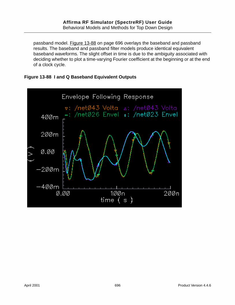
Affirma RF Simulator (SpectreRF) User GuideBehavioral Models and Methods for Top Down Design
passband model. Figure 13-88 on page 696 overlays the baseband and passbandresults. The baseband and passband filter models produce identical equivalentbaseband waveforms. The slight offset in time is due to the ambiguity associated withdeciding whether to plot a time-varying Fourier coefficient at the beginning or at the endof a clock cycle.
Figure 13-88 I and Q Baseband Equivalent Outputs
April 2001 696 Product Version 4.4.6
Affirma RF Simulator (SpectreRF) User GuideBehavioral Models and Methods for Top Down Design
BB_Loss
The BB_loss element is designed to be used with error vector magnitude (EVM) calculations.EVM is defined in terms of an ideal receiver or transmitter. If you want to remove a filter’sresponse from the ideal receiver model while leaving only the passband attenuation, replacethe filter with a BB_loss element and give it the same insertion loss as the filter. There is nopassband view or counterpart for this model because a passband EVM analysis is notpractical in this release.
April 2001 697 Product Version 4.4.6
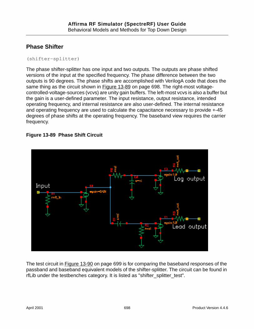
Affirma RF Simulator (SpectreRF) User GuideBehavioral Models and Methods for Top Down Design
Phase Shifter
(shifter-splitter)
The phase shifter-splitter has one input and two outputs. The outputs are phase shiftedversions of the input at the specified frequency. The phase difference between the twooutputs is 90 degrees. The phase shifts are accomplished with VerilogA code that does thesame thing as the circuit shown in Figure 13-89 on page 698. The right-most voltage-controlled-voltage-sources (vcvs) are unity gain buffers. The left-most vcvs is also a buffer butthe gain is a user-defined parameter. The input resistance, output resistance, intendedoperating frequency, and internal resistance are also user-defined. The internal resistanceand operating frequency are used to calculate the capacitance necessary to provide +-45degrees of phase shifts at the operating frequency. The baseband view requires the carrierfrequency.
Figure 13-89 Phase Shift Circuit
The test circuit in Figure 13-90 on page 699 is for comparing the baseband responses of thepassband and baseband equivalent models of the shifter-splitter. The circuit can be found inrfLib under the testbenches category. It is listed as "shifter_splitter_test".
April 2001 698 Product Version 4.4.6
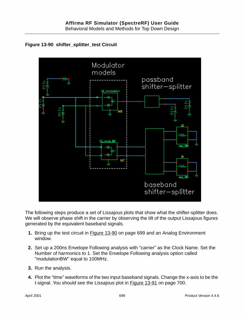
Affirma RF Simulator (SpectreRF) User GuideBehavioral Models and Methods for Top Down Design
Figure 13-90 shifter_splitter_test Circuit
The following steps produce a set of Lissajous plots that show what the shifter-splitter does.We will observe phase shift in the carrier by observing the tilt of the output Lissajous figuresgenerated by the equivalent baseband signals.
1. Bring up the test circuit in Figure 13-90 on page 699 and an Analog Environmentwindow.
2. Set up a 200ns Envelope Following analysis with “carrier” as the Clock Name. Set theNumber of harmonics to 1. Set the Envelope Following analysis option called"modulationBW" equal to 100MHz.
3. Run the analysis.
4. Plot the “time” waveforms of the two input baseband signals. Change the x-axis to be theI-signal. You should see the Lissajous plot in Figure 13-91 on page 700.
April 2001 699 Product Version 4.4.6
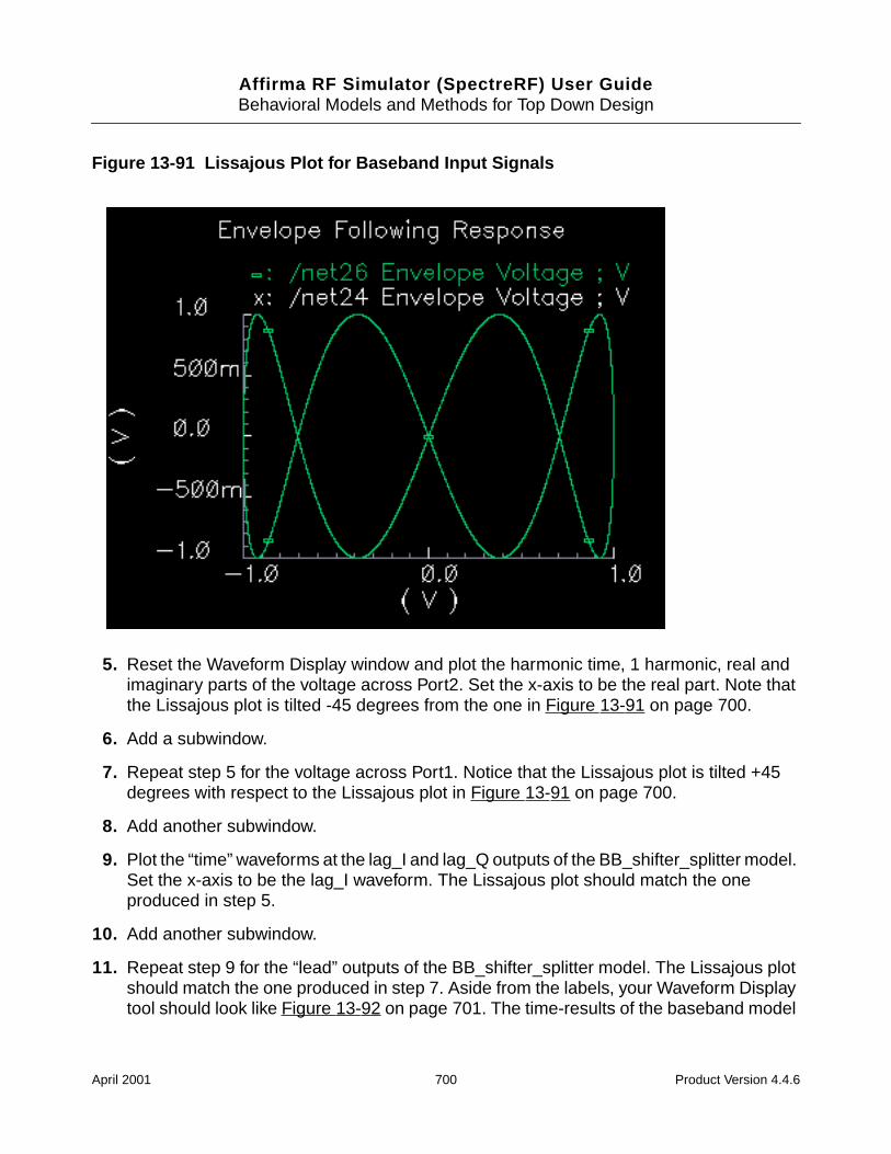
Affirma RF Simulator (SpectreRF) User GuideBehavioral Models and Methods for Top Down Design
Figure 13-91 Lissajous Plot for Baseband Input Signals
5. Reset the Waveform Display window and plot the harmonic time, 1 harmonic, real andimaginary parts of the voltage across Port2. Set the x-axis to be the real part. Note thatthe Lissajous plot is tilted -45 degrees from the one in Figure 13-91 on page 700.
6. Add a subwindow.
7. Repeat step 5 for the voltage across Port1. Notice that the Lissajous plot is tilted +45degrees with respect to the Lissajous plot in Figure 13-91 on page 700.
8. Add another subwindow.
9. Plot the “time” waveforms at the lag_I and lag_Q outputs of the BB_shifter_splitter model.Set the x-axis to be the lag_I waveform. The Lissajous plot should match the oneproduced in step 5.
10. Add another subwindow.
11. Repeat step 9 for the “lead” outputs of the BB_shifter_splitter model. The Lissajous plotshould match the one produced in step 7. Aside from the labels, your Waveform Displaytool should look like Figure 13-92 on page 701. The time-results of the baseband model
April 2001 700 Product Version 4.4.6
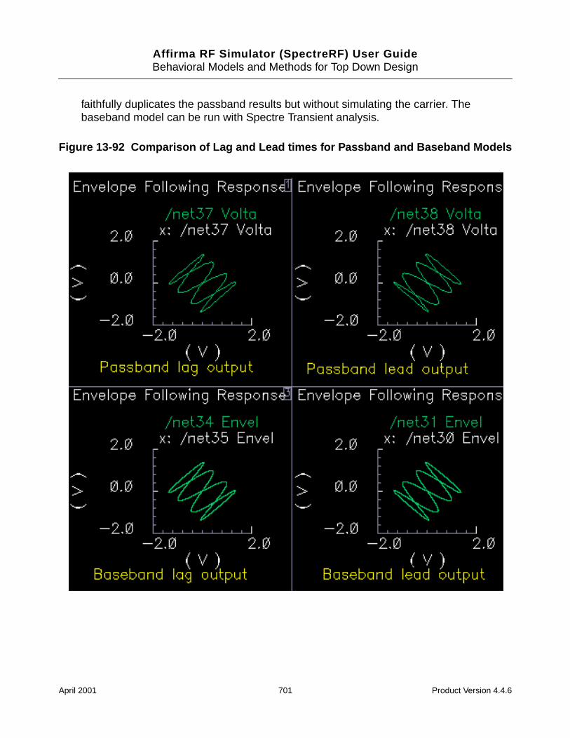
Affirma RF Simulator (SpectreRF) User GuideBehavioral Models and Methods for Top Down Design
faithfully duplicates the passband results but without simulating the carrier. Thebaseband model can be run with Spectre Transient analysis.
Figure 13-92 Comparison of Lag and Lead times for Passband and Baseband Models
April 2001 701 Product Version 4.4.6
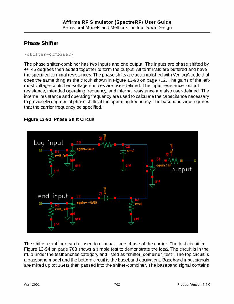
Affirma RF Simulator (SpectreRF) User GuideBehavioral Models and Methods for Top Down Design
Phase Shifter
(shifter-combiner)
The phase shifter-combiner has two inputs and one output. The inputs are phase shifted by+/- 45 degrees then added together to form the output. All terminals are buffered and havethe specified terminal resistances. The phase shifts are accomplished with VerilogA code thatdoes the same thing as the circuit shown in Figure 13-93 on page 702. The gains of the left-most voltage-controlled-voltage sources are user-defined. The input resistance, outputresistance, intended operating frequency, and internal resistance are also user-defined. Theinternal resistance and operating frequency are used to calculate the capacitance necessaryto provide 45 degrees of phase shifts at the operating frequency. The baseband view requiresthat the carrier frequency be specified.
Figure 13-93 Phase Shift Circuit
The shifter-combiner can be used to eliminate one phase of the carrier. The test circuit inFigure 13-94 on page 703 shows a simple test to demonstrate the idea. The circuit is in therfLib under the testbenches category and listed as "shifter_combiner_test". The top circuit isa passband model and the bottom circuit is the baseband equivalent. Baseband input signalsare mixed up tot 1GHz then passed into the shifter-combiner. The baseband signal contains
April 2001 702 Product Version 4.4.6
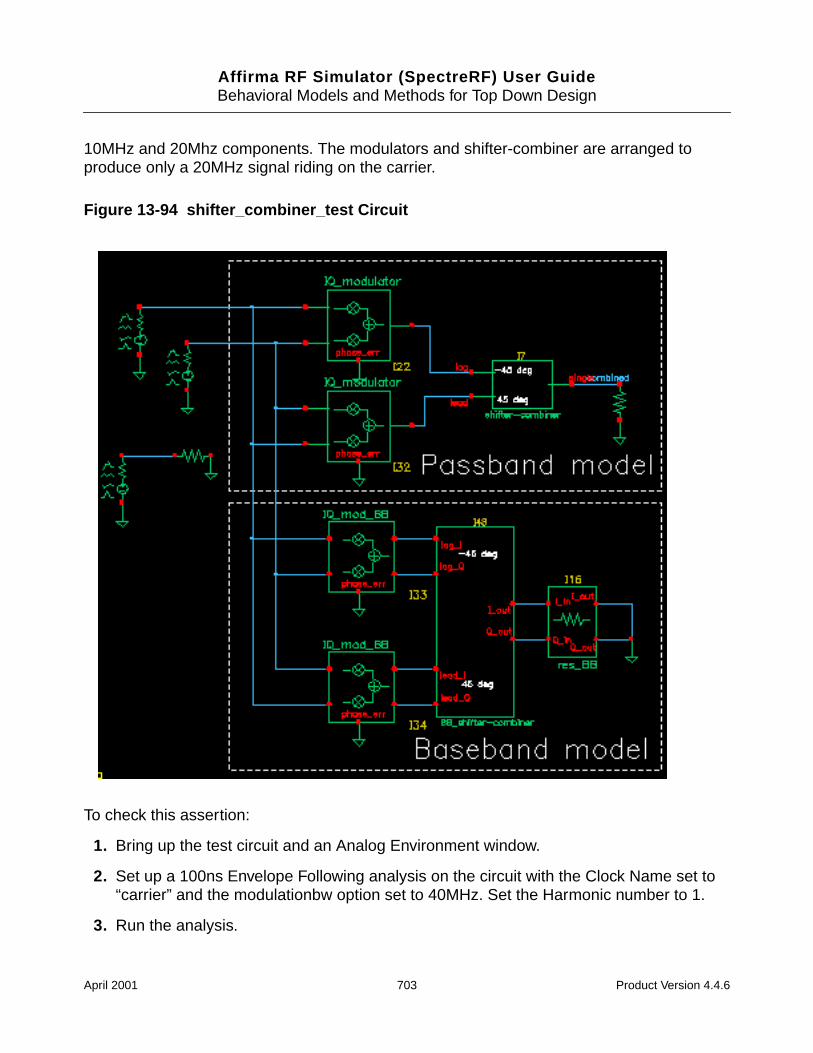
Affirma RF Simulator (SpectreRF) User GuideBehavioral Models and Methods for Top Down Design
10MHz and 20Mhz components. The modulators and shifter-combiner are arranged toproduce only a 20MHz signal riding on the carrier.
Figure 13-94 shifter_combiner_test Circuit
To check this assertion:
1. Bring up the test circuit and an Analog Environment window.
2. Set up a 100ns Envelope Following analysis on the circuit with the Clock Name set to“carrier” and the modulationbw option set to 40MHz. Set the Harmonic number to 1.
3. Run the analysis.
April 2001 703 Product Version 4.4.6
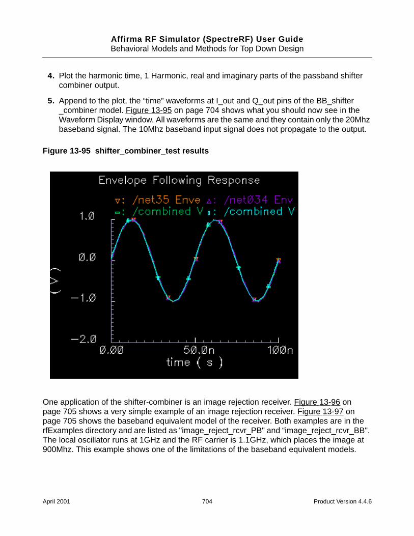
Affirma RF Simulator (SpectreRF) User GuideBehavioral Models and Methods for Top Down Design
4. Plot the harmonic time, 1 Harmonic, real and imaginary parts of the passband shiftercombiner output.
5. Append to the plot, the “time” waveforms at I_out and Q_out pins of the BB_shifter_combiner model. Figure 13-95 on page 704 shows what you should now see in theWaveform Display window. All waveforms are the same and they contain only the 20Mhzbaseband signal. The 10Mhz baseband input signal does not propagate to the output.
Figure 13-95 shifter_combiner_test results
One application of the shifter-combiner is an image rejection receiver. Figure 13-96 onpage 705 shows a very simple example of an image rejection receiver. Figure 13-97 onpage 705 shows the baseband equivalent model of the receiver. Both examples are in therfExamples directory and are listed as "image_reject_rcvr_PB" and “image_reject_rcvr_BB".The local oscillator runs at 1GHz and the RF carrier is 1.1GHz, which places the image at900Mhz. This example shows one of the limitations of the baseband equivalent models.
April 2001 704 Product Version 4.4.6
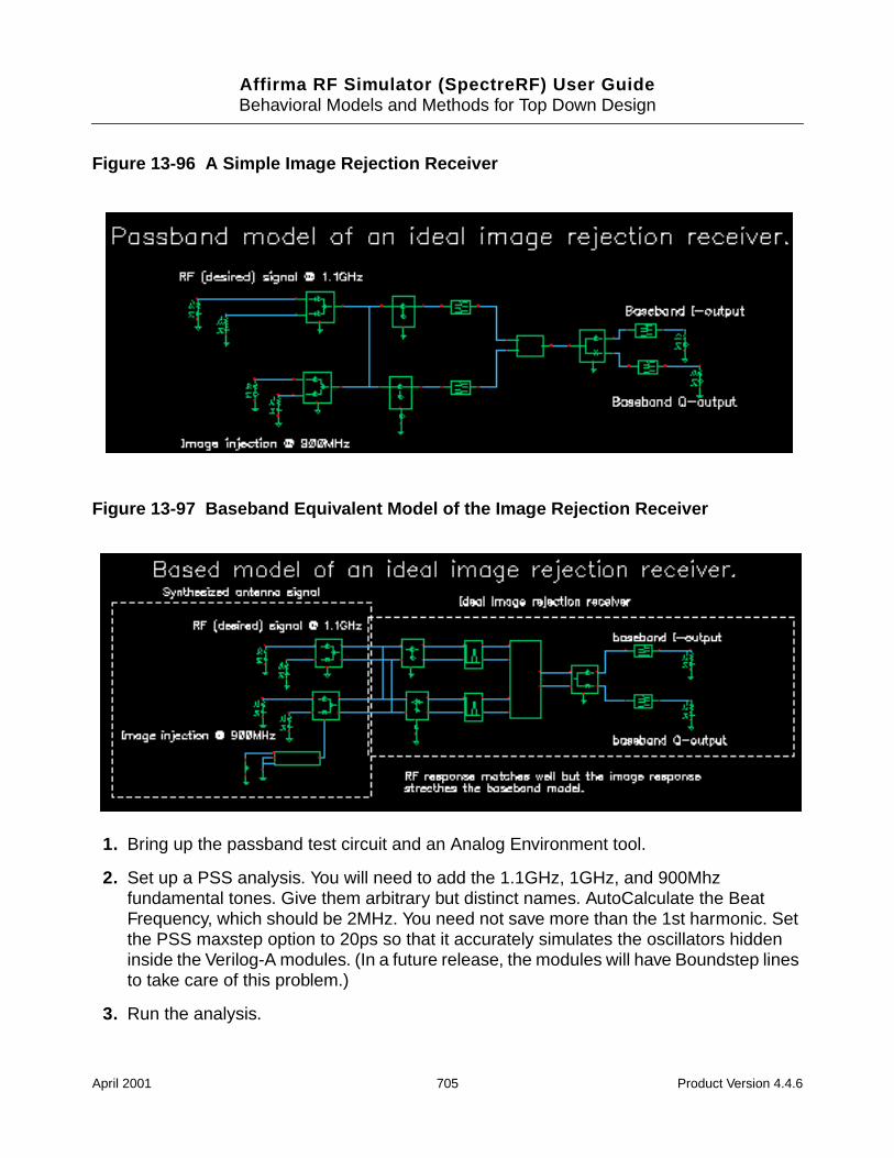
Affirma RF Simulator (SpectreRF) User GuideBehavioral Models and Methods for Top Down Design
Figure 13-96 A Simple Image Rejection Receiver
Figure 13-97 Baseband Equivalent Model of the Image Rejection Receiver
1. Bring up the passband test circuit and an Analog Environment tool.
2. Set up a PSS analysis. You will need to add the 1.1GHz, 1GHz, and 900Mhzfundamental tones. Give them arbitrary but distinct names. AutoCalculate the BeatFrequency, which should be 2MHz. You need not save more than the 1st harmonic. Setthe PSS maxstep option to 20ps so that it accurately simulates the oscillators hiddeninside the Verilog-A modules. (In a future release, the modules will have Boundstep linesto take care of this problem.)
3. Run the analysis.
April 2001 705 Product Version 4.4.6
Affirma RF Simulator (SpectreRF) User GuideBehavioral Models and Methods for Top Down Design
4. Plot the voltages across Ports 5 and 6. Set the x-axis to be the voltage across Port 6.This is a Lissajous plot of the desired baseband signal, the one riding on the 1.1GHzcarrier.
5. Add a subwindow.
6. Plot the voltages across Ports 8 and 7. Set the x-axis to be the voltage across Port 8.This is a Lissajous plot of the undesired baseband signal, the signal riding on the imageof the carrier at 900MHz.
7. Add another subwindow.
8. Plot the I and Q- baseband outputs. Set the x-axis to be the I-output. The Lissajous plotis a tilted version of the desired baseband signal, indicating that most of the image wassuccessfully rejected.
9. Bring up the baseband equivalent receiver model and another Analog Environment tool.
10. Run a 10us Transient analysis with 9.5us as the output start in the analysis options andmaxstep set to 250ps. The phase_err pin on the image signal generator is being drivento spin the output at 200MHz, the frequency difference between the desired frequencyand image frequency.
11. Add another subwindow to the Waveform Display tool showing the passband results andmake sure it is active.
12. Plot the I and Q baseband outputs from the baseband equivalent receiver model. Set thex-axis to be the I-output. You may need to make the scales on the last two plots are thesame. Aside from the labels, the Waveform Display tool should look like Figure 13-98 onpage 707.
April 2001 706 Product Version 4.4.6
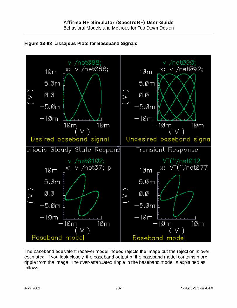
Affirma RF Simulator (SpectreRF) User GuideBehavioral Models and Methods for Top Down Design
Figure 13-98 Lissajous Plots for Baseband Signals
The baseband equivalent receiver model indeed rejects the image but the rejection is over-estimated. If you look closely, the baseband output of the passband model contains moreripple from the image. The over-attenuated ripple in the baseband model is explained asfollows.
April 2001 707 Product Version 4.4.6
Affirma RF Simulator (SpectreRF) User GuideBehavioral Models and Methods for Top Down Design
Recall the rotating reference frame analogy for baseband modeling. With respect to therotating 1.1GHz reference frame, the image signals rotate counter-clockwise at twice the IF,200MHz in this case. The lower left block in the baseband receiver model spins the modulatoroutput at -200Mhz by ramping the phase error pin. The -200MHz signal propagates throughthe IF bandpass filters, as it should, because the response of the baseband model of the filterpeaks at DC and at minus 200MHz. The trouble occurs in the final downconversion tobaseband. In the baseband model, the final low pass filters severely attenuate the -200Mhzimage signal. However, in the passband model, image power at minus 100MHz contributesto the baseband signal through the low pass filters with less attenuation.
This example highlights one of the limitations of baseband equivalent models: at any point inthe system, the signal should not have a bandwidth larger than any carrier (RF or IF) of thesystem. For this example, the baseband model is only valid for input RF signals between1GHz and 1.2GHz.
The limitation is somewhat moot because the idea behind a baseband equivalent model is tosuppress all carriers. To simulate the image response with the baseband model we had toinclude a 200MHz source! We would have been better off simply not suppressing the 100MHzIF carrier, i.e. using baseband models for the RF stages but passband models for the IFstages.
In summary, an all-baseband equivalent model of an image rejection receiver is only good forsimulating the response to the desired RF signal, not the image response.
April 2001 708 Product Version 4.4.6
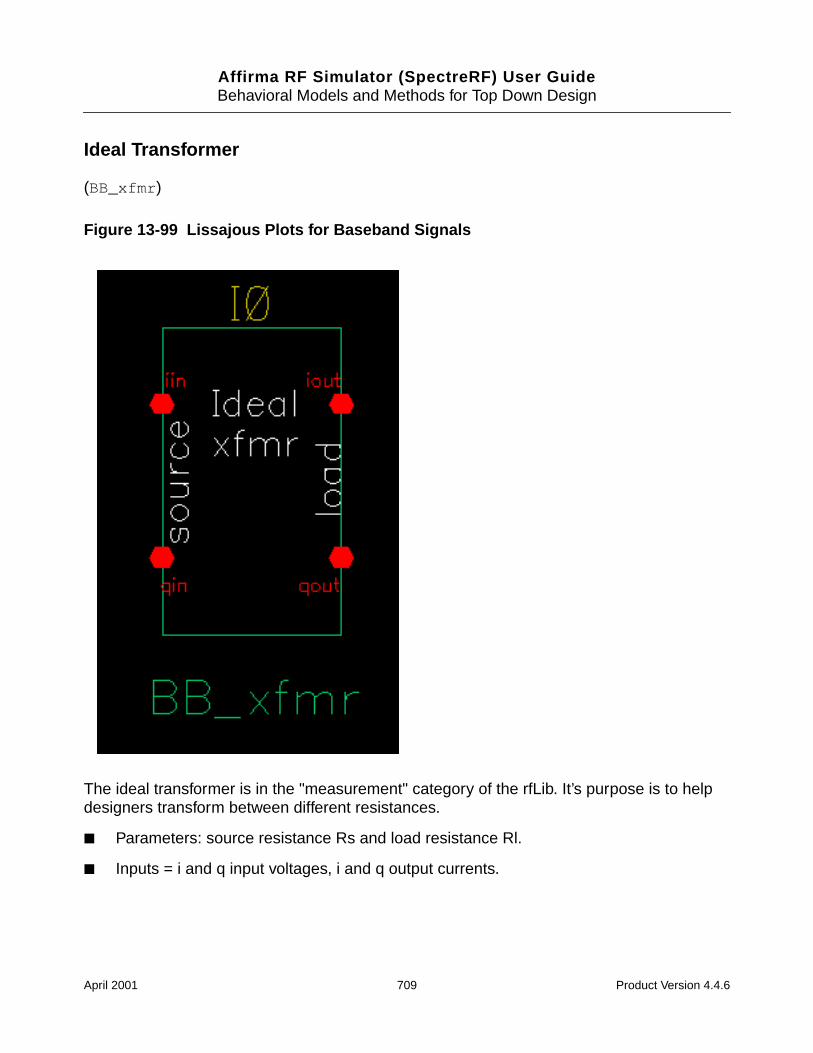
Affirma RF Simulator (SpectreRF) User GuideBehavioral Models and Methods for Top Down Design
Ideal Transformer
(BB_xfmr )
Figure 13-99 Lissajous Plots for Baseband Signals
The ideal transformer is in the "measurement" category of the rfLib. It’s purpose is to helpdesigners transform between different resistances.
Parameters: source resistance Rs and load resistance Rl.
Inputs = i and q input voltages, i and q output currents.
April 2001 709 Product Version 4.4.6
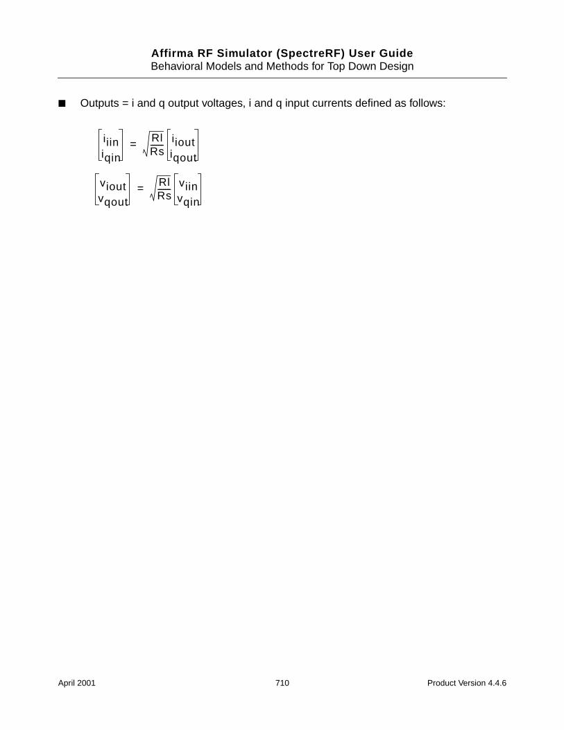
Affirma RF Simulator (SpectreRF) User GuideBehavioral Models and Methods for Top Down Design
Outputs = i and q output voltages, i and q input currents defined as follows:
iiiniqin
RlRs------- iiout
iqout=
vioutvqout
RlRs------- viin
vqin=
April 2001 710 Product Version 4.4.6
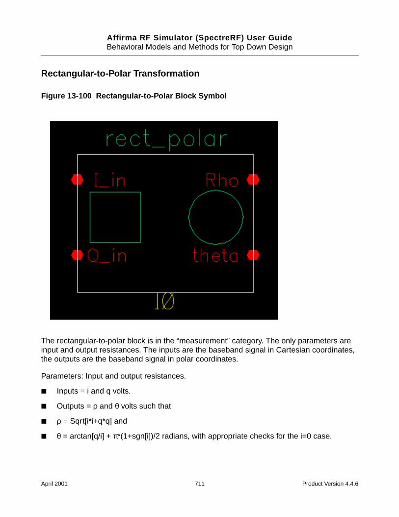
Affirma RF Simulator (SpectreRF) User GuideBehavioral Models and Methods for Top Down Design
Rectangular-to-Polar Transformation
Figure 13-100 Rectangular-to-Polar Block Symbol
The rectangular-to-polar block is in the “measurement” category. The only parameters areinput and output resistances. The inputs are the baseband signal in Cartesian coordinates,the outputs are the baseband signal in polar coordinates.
Parameters: Input and output resistances.
Inputs = i and q volts.
Outputs = ρ and θ volts such that
ρ = Sqrt[i*i+q*q] and
θ = arctan[q/i] + π*(1+sgn[i])/2 radians, with appropriate checks for the i=0 case.
April 2001 711 Product Version 4.4.6
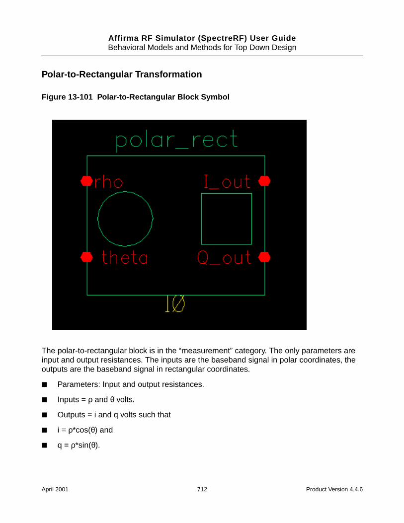
Affirma RF Simulator (SpectreRF) User GuideBehavioral Models and Methods for Top Down Design
Polar-to-Rectangular Transformation
Figure 13-101 Polar-to-Rectangular Block Symbol
The polar-to-rectangular block is in the “measurement” category. The only parameters areinput and output resistances. The inputs are the baseband signal in polar coordinates, theoutputs are the baseband signal in rectangular coordinates.
Parameters: Input and output resistances.
Inputs = ρ and θ volts.
Outputs = i and q volts such that
i = ρ*cos(θ) and
q = ρ*sin(θ).
April 2001 712 Product Version 4.4.6
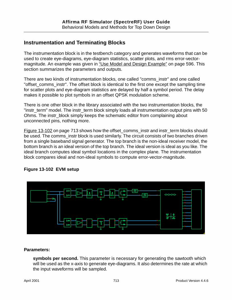
Affirma RF Simulator (SpectreRF) User GuideBehavioral Models and Methods for Top Down Design
Instrumentation and Terminating Blocks
The instrumentation block is in the testbench category and generates waveforms that can beused to create eye-diagrams, eye-diagram statistics, scatter plots, and rms error-vector-magnitude. An example was given in “Use Model and Design Example” on page 596. Thissection summarizes the parameters and outputs.
There are two kinds of instrumentation blocks, one called "comms_instr" and one called"offset_comms_instr". The offset block is identical to the first one except the sampling timefor scatter plots and eye-diagram statistics are delayed by half a symbol period. The delaymakes it possible to plot symbols in an offset QPSK modulation scheme.
There is one other block in the library associated with the two instrumentation blocks, the"instr_term" model. The instr_term block simply loads all instrumentation output pins with 50Ohms. The instr_block simply keeps the schematic editor from complaining aboutunconnected pins, nothing more.
Figure 13-102 on page 713 shows how the offset_comms_instr and instr_term blocks shouldbe used. The comms_instr block is used similarly. The circuit consists of two branches drivenfrom a single baseband signal generator. The top branch is the non-ideal receiver model, thebottom branch is an ideal version of the top branch. The ideal version is ideal as you like. Theideal branch computes ideal symbol locations in the complex plane. The instrumentationblock compares ideal and non-ideal symbols to compute error-vector-magnitude.
Figure 13-102 EVM setup
Parameters:
symbols per second. This parameter is necessary for generating the sawtooth whichwill be used as the x-axis to generate eye-diagrams. It also determines the rate at whichthe input waveforms will be sampled.
April 2001 713 Product Version 4.4.6
Affirma RF Simulator (SpectreRF) User GuideBehavioral Models and Methods for Top Down Design
I-sampling delay. This parameter sets the phase of the symbol sampler. It is referencedto the eye-diagram of the I-output. Estimate the optimal delay by doing one simulationjust to get the eye-diagram. The optimal delay is the time from the leftmost part of theeye-diagram, which should be zero, to the time at which they eye is widest.
number of symbols. This is the number of symbols to sweep in the eye-diagram.Sweeping two symbols ensures that you will see at least one continuous eye, if it is open.
max, min eye-diagram volts, and number of hstgm bins. These parameters are usedto compute the bins which define the eye-diagram histogram. The bin width equals (maxvoltage-min voltage)/(number of bins). The histogram shows the distribution of the I_involtage at the sampling instant.
I-noise and Q-noise(volts^2). These parameters set the variance of Gaussian randomvariables which can be added to the received symbols before anything is computed orplotted.
statistics start time. This parameter delays the start of any statistical computations.The purpose is to exclude start-up transients from the statistics.
input resistance. This parameter is the input resistance of the input terminals of theinstrumentation block.
Eye-diagrams. To generate an eye-diagram of the I-input signal, plot the sawtooth andI-eye outputs in one waveform display tool. Change the x-axis to be the sawtooth. Thisis done through the x-axis menu in the waveform display tool. The procedure forgenerating an eye-diagram of the Q-output is the same except you use the Q-eye output.
Histograms. You can only generate a histogram of the I-input signal. The histogramshows the distribution of the I-input voltage at the sampling instant. To generate ahistogram, plot the eye_hist and eye_count_hist outputs in the same waveform displaywindow. Change the x-axis to be the eye-hist signal then change the plot to "bar".
Eye-diagram statistics. The ave_eye output is the average absolute value of the I-inputsignal at the sampling instant. The root_var_eye output is the square root of the varianceof the absolute value of the I-input voltage at the sampling instant. The voltages at theseoutput pins represent running estimates of the associated statistics.
Scatter plots. A scatter plot is the I-input and Q-input samples plotted against eachother. The scatter plot shows the locations of the received symbols. To generate a scatterplot, plot I_scatter and Q_scatter in the same waveform display window then change thex-axis to be the I_scatter signal. Finally, change the plot to plot data points only. A scatterplot of the reference model can be generated similarly by replacing I_scatter andQ_scatter with Iref_scatter and Qref_scatter.
rms Error Vector Magnitude. The rms EVM is defined as the square root of the sum ofthe squares of the vectorial differences between the ideal and non-ideal received
April 2001 714 Product Version 4.4.6

Affirma RF Simulator (SpectreRF) User GuideBehavioral Models and Methods for Top Down Design
symbols, normalized to the rms value of the magnitude of the ideal received symbols.The output voltage at this pin is represents a running calculation of the rms EVM. Thenormalized EVM is in percent.
April 2001 715 Product Version 4.4.6
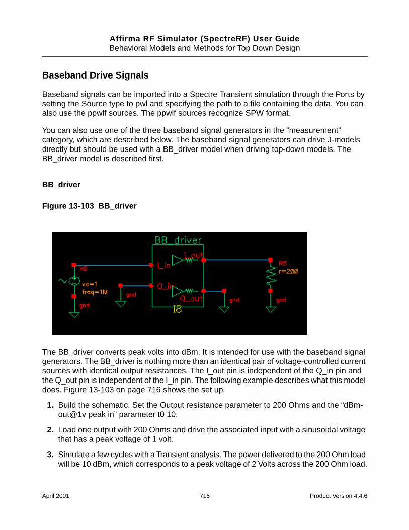
Affirma RF Simulator (SpectreRF) User GuideBehavioral Models and Methods for Top Down Design
Baseband Drive Signals
Baseband signals can be imported into a Spectre Transient simulation through the Ports bysetting the Source type to pwl and specifying the path to a file containing the data. You canalso use the ppwlf sources. The ppwlf sources recognize SPW format.
You can also use one of the three baseband signal generators in the “measurement”category, which are described below. The baseband signal generators can drive J-modelsdirectly but should be used with a BB_driver model when driving top-down models. TheBB_driver model is described first.
BB_driver
Figure 13-103 BB_driver
The BB_driver converts peak volts into dBm. It is intended for use with the baseband signalgenerators. The BB_driver is nothing more than an identical pair of voltage-controlled currentsources with identical output resistances. The I_out pin is independent of the Q_in pin andthe Q_out pin is independent of the I_in pin. The following example describes what this modeldoes. Figure 13-103 on page 716 shows the set up.
1. Build the schematic. Set the Output resistance parameter to 200 Ohms and the “dBm-out@1v peak in” parameter t0 10.
2. Load one output with 200 Ohms and drive the associated input with a sinusoidal voltagethat has a peak voltage of 1 volt.
3. Simulate a few cycles with a Transient analysis. The power delivered to the 200 Ohm loadwill be 10 dBm, which corresponds to a peak voltage of 2 Volts across the 200 Ohm load.
April 2001 716 Product Version 4.4.6
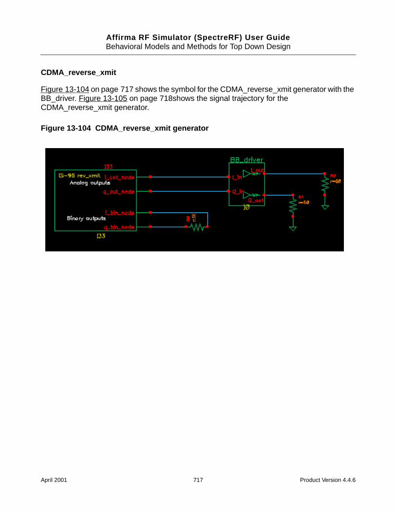
Affirma RF Simulator (SpectreRF) User GuideBehavioral Models and Methods for Top Down Design
CDMA_reverse_xmit
Figure 13-104 on page 717 shows the symbol for the CDMA_reverse_xmit generator with theBB_driver. Figure 13-105 on page 718shows the signal trajectory for theCDMA_reverse_xmit generator.
Figure 13-104 CDMA_reverse_xmit generator
April 2001 717 Product Version 4.4.6
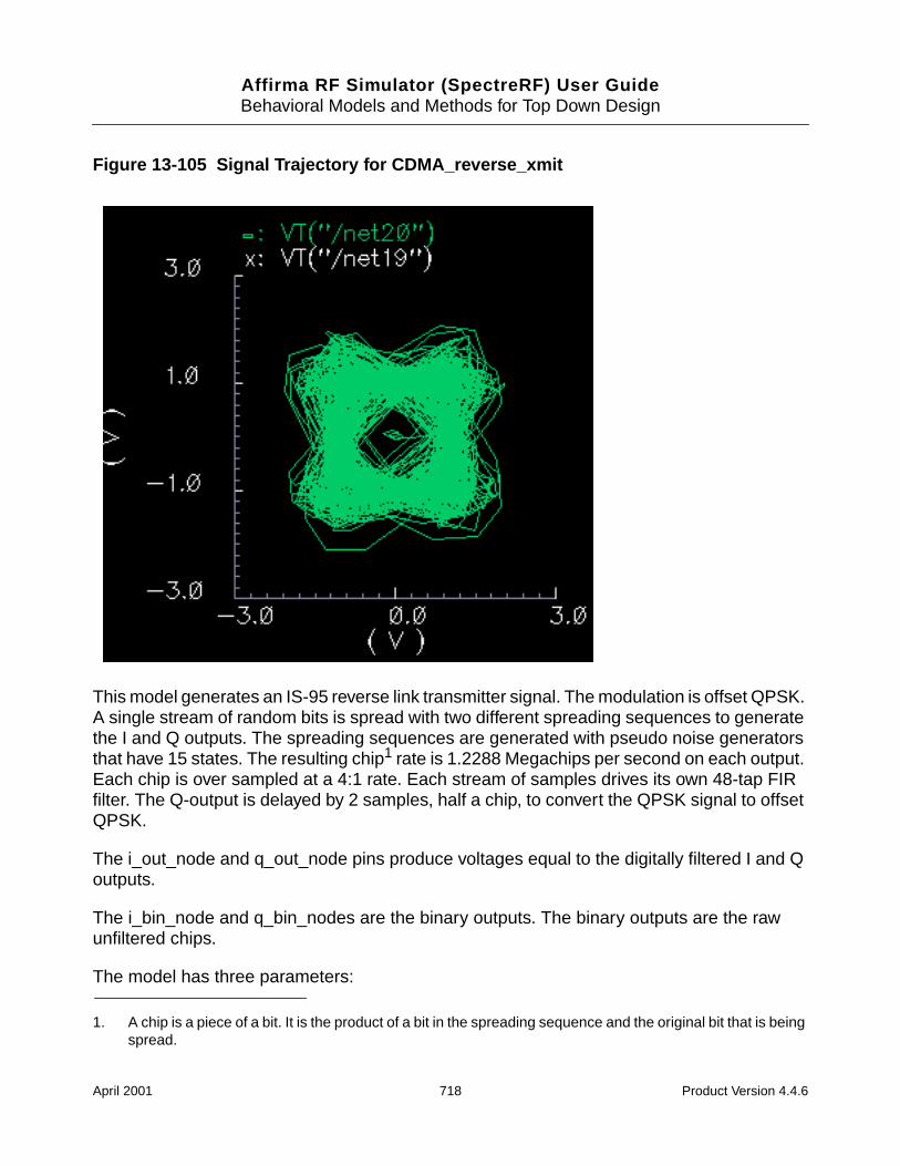
Affirma RF Simulator (SpectreRF) User GuideBehavioral Models and Methods for Top Down Design
Figure 13-105 Signal Trajectory for CDMA_reverse_xmit
This model generates an IS-95 reverse link transmitter signal. The modulation is offset QPSK.A single stream of random bits is spread with two different spreading sequences to generatethe I and Q outputs. The spreading sequences are generated with pseudo noise generatorsthat have 15 states. The resulting chip1 rate is 1.2288 Megachips per second on each output.Each chip is over sampled at a 4:1 rate. Each stream of samples drives its own 48-tap FIRfilter. The Q-output is delayed by 2 samples, half a chip, to convert the QPSK signal to offsetQPSK.
The i_out_node and q_out_node pins produce voltages equal to the digitally filtered I and Qoutputs.
The i_bin_node and q_bin_nodes are the binary outputs. The binary outputs are the rawunfiltered chips.
The model has three parameters:
1. A chip is a piece of a bit. It is the product of a bit in the spreading sequence and the original bit that is beingspread.
April 2001 718 Product Version 4.4.6
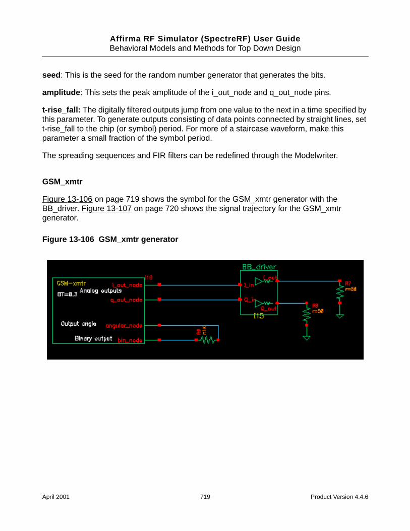
Affirma RF Simulator (SpectreRF) User GuideBehavioral Models and Methods for Top Down Design
seed : This is the seed for the random number generator that generates the bits.
amplitude : This sets the peak amplitude of the i_out_node and q_out_node pins.
t-rise_fall: The digitally filtered outputs jump from one value to the next in a time specified bythis parameter. To generate outputs consisting of data points connected by straight lines, sett-rise_fall to the chip (or symbol) period. For more of a staircase waveform, make thisparameter a small fraction of the symbol period.
The spreading sequences and FIR filters can be redefined through the Modelwriter.
GSM_xmtr
Figure 13-106 on page 719 shows the symbol for the GSM_xmtr generator with theBB_driver. Figure 13-107 on page 720 shows the signal trajectory for the GSM_xmtrgenerator.
Figure 13-106 GSM_xmtr generator
April 2001 719 Product Version 4.4.6
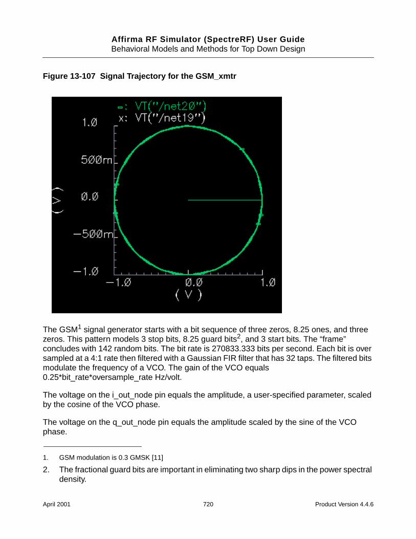
Affirma RF Simulator (SpectreRF) User GuideBehavioral Models and Methods for Top Down Design
Figure 13-107 Signal Trajectory for the GSM_xmtr
The GSM1 signal generator starts with a bit sequence of three zeros, 8.25 ones, and threezeros. This pattern models 3 stop bits, 8.25 guard bits2, and 3 start bits. The “frame”concludes with 142 random bits. The bit rate is 270833.333 bits per second. Each bit is oversampled at a 4:1 rate then filtered with a Gaussian FIR filter that has 32 taps. The filtered bitsmodulate the frequency of a VCO. The gain of the VCO equals0.25*bit_rate*oversample_rate Hz/volt.
The voltage on the i_out_node pin equals the amplitude, a user-specified parameter, scaledby the cosine of the VCO phase.
The voltage on the q_out_node pin equals the amplitude scaled by the sine of the VCOphase.
1. GSM modulation is 0.3 GMSK [11]
2. The fractional guard bits are important in eliminating two sharp dips in the power spectraldensity.
April 2001 720 Product Version 4.4.6
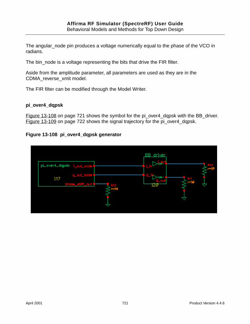
Affirma RF Simulator (SpectreRF) User GuideBehavioral Models and Methods for Top Down Design
The angular_node pin produces a voltage numerically equal to the phase of the VCO inradians.
The bin_node is a voltage representing the bits that drive the FIR filter.
Aside from the amplitude parameter, all parameters are used as they are in theCDMA_reverse_xmit model.
The FIR filter can be modified through the Model Writer.
pi_over4_dqpsk
Figure 13-108 on page 721 shows the symbol for the pi_over4_dqpsk with the BB_driver.Figure 13-109 on page 722 shows the signal trajectory for the pi_over4_dqpsk.
Figure 13-108 pi_over4_dqpsk generator
April 2001 721 Product Version 4.4.6
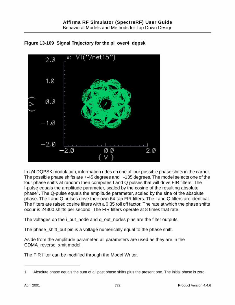
Affirma RF Simulator (SpectreRF) User GuideBehavioral Models and Methods for Top Down Design
Figure 13-109 Signal Trajectory for the pi_over4_dqpsk
In π/4 DQPSK modulation, information rides on one of four possible phase shifts in the carrier.The possible phase shifts are +-45 degrees and +-135 degrees. The model selects one of thefour phase shifts at random then computes I and Q pulses that will drive FIR filters. TheI-pulse equals the amplitude parameter, scaled by the cosine of the resulting absolutephase1. The Q-pulse equals the amplitude parameter, scaled by the sine of the absolutephase. The I and Q pulses drive their own 64-tap FIR filters. The I and Q filters are identical.The filters are raised cosine filters with a 0.35 roll off factor. The rate at which the phase shiftsoccur is 24300 shifts per second. The FIR filters operate at 8 times that rate.
The voltages on the i_out_node and q_out_nodes pins are the filter outputs.
The phase_shift_out pin is a voltage numerically equal to the phase shift.
Aside from the amplitude parameter, all parameters are used as they are in theCDMA_reverse_xmit model.
The FIR filter can be modified through the Model Writer.
1. Absolute phase equals the sum of all past phase shifts plus the present one. The initial phase is zero.
April 2001 722 Product Version 4.4.6
Affirma RF Simulator (SpectreRF) User GuideBehavioral Models and Methods for Top Down Design
ress,
m-
ny,
Inc,
C
ci-
References1. M. Jeruchim, P. Balaban, K. Shanmugan, “Simulation of Communication Systems”, Plenum P
1992.2. E. Lee, D. Messerschmitt, “Digital Communication”, Kluwer Academic Publishers, 19943. A. Fitzgerald, C. Kingsley Jr.,S Umans, "Electric Machinery", Fifth edition, McGraw Hill4. R. Stein and W. Hunt Jr., “Electric Power System Components”, Van Nostrand Reinhold Co
pany, 1979.5. W. Leonhard, “Control of Electrical Drives”, Springer-Verlag 1990.6. P. Kraus and O. Wasynchuk, “Electromechanical Motion Device”s, McGraw-Hill Book Compa
1989.7. P. Vas, “Vector Control of AC Machines”, Oxford University Press, 19908. G. Kron, “A Short Course in Tensor Analysis for Electrical Engineers” , John Wiley and Sons,
1942.9. J. Chen, “Rotor Reference Frame Models of a Multiloop 2-phase Motor Drive in Brushless D
and MicroStepping Modes”, 1995 Intersociety Energy Conversion Engineering Conference,Orlando, FLA.
10.A. Harrysson, M. Ziren, “System Level Simulations of a Receiver for W-CDMA”, Master of Sence Thesis, Department of Applied Electronics, Lund Institute of Technology, 12/99.
11.T. Rappaport, “Wireless Communications, Principles and Practice”. 1996. Prentice Hall.
April 2001 723 Product Version 4.4.6
Affirma RF Simulator (SpectreRF) User Guide
AOscillator Noise Analysis
The procedures described in this appendix are deliberately broad and generic. Requirementsfor your specific design might dictate procedures slightly different from those described here.
You can use this document in the following three ways:
To learn background theory about phase noise
To learn how the Spectre®RF circuit simulator noise calculations are related to commonphase noise models
To learn ways to use and troubleshoot SpectreRF phase noise calculations and toanswer common questions
These procedures are intended for SpectreRF users who analyze oscillator noise. Usersmust have a working familiarity with SpectreRF simulation and its operating principles. Inparticular, readers must understand the SpectreRF PSS and PNOISE analyses. Forinformation about performing these analyses, consult the oscillator chapter in the Spectreonline documentation library. Reading the SpectreRF Theory document in the online libraryis also recommended.
In RF systems, local oscillator phase noise can limit the final system performance. TheSpectreRF circuit simulator lets you rigorously characterize the noise performance ofoscillator elements. This appendix explains phase noise, tells how it occurs, and shows howto calculate phase noise using the SpectreRF circuit simulator.
The “Phase Noise Primer” on page 725 discusses how phase noise occurs and provides asimple illustrative example.
“Calculating Phase Noise” on page 737 provides some suggestions for successful andefficient analysis of oscillators and discusses the limitations of the simulator.
“Troubleshooting Phase Noise Calculations” on page 739 explains troubleshooting methodsfor difficult simulations.
“Frequently Asked Questions” on page 744 answers some commonly asked questions aboutphase noise and the SpectreRF circuit simulator.
April 2001 724 Product Version 4.4.6
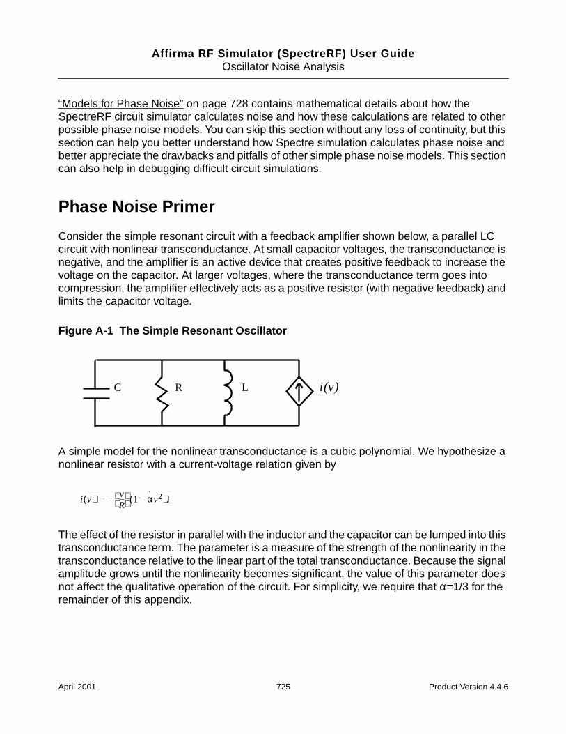
Affirma RF Simulator (SpectreRF) User GuideOscillator Noise Analysis
“Models for Phase Noise” on page 728 contains mathematical details about how theSpectreRF circuit simulator calculates noise and how these calculations are related to otherpossible phase noise models. You can skip this section without any loss of continuity, but thissection can help you better understand how Spectre simulation calculates phase noise andbetter appreciate the drawbacks and pitfalls of other simple phase noise models. This sectioncan also help in debugging difficult circuit simulations.
Phase Noise Primer
Consider the simple resonant circuit with a feedback amplifier shown below, a parallel LCcircuit with nonlinear transconductance. At small capacitor voltages, the transconductance isnegative, and the amplifier is an active device that creates positive feedback to increase thevoltage on the capacitor. At larger voltages, where the transconductance term goes intocompression, the amplifier effectively acts as a positive resistor (with negative feedback) andlimits the capacitor voltage.
Figure A-1 The Simple Resonant Oscillator
A simple model for the nonlinear transconductance is a cubic polynomial. We hypothesize anonlinear resistor with a current-voltage relation given by
The effect of the resistor in parallel with the inductor and the capacitor can be lumped into thistransconductance term. The parameter is a measure of the strength of the nonlinearity in thetransconductance relative to the linear part of the total transconductance. Because the signalamplitude grows until the nonlinearity becomes significant, the value of this parameter doesnot affect the qualitative operation of the circuit. For simplicity, we require that α=1/3 for theremainder of this appendix.
C R L i(v)
i v( ) vR---
1 αv2–( ).˙–=
April 2001 725 Product Version 4.4.6
Affirma RF Simulator (SpectreRF) User GuideOscillator Noise Analysis
After some renormalization1 of variables, the differential equations describing the oscillatorcan be written in the following form
In these equations, where v and i give the normalized capacitor voltage and inductor current,respectively, and ξ(t) is a small-signal excitation such as white Gaussian noise. Q = R/ω0 Lis the quality factor of an RLC circuit made by replacing the nonlinear transconductance by apositive resistance R.
These equations describe the familiar van der Pol oscillator system. This model includesmany of the qualitative aspects of oscillator dynamics, yet it is simple enough to analyze indetail. Many more complicated oscillators that operate in a weakly nonlinear mode can beapproximated with this model by using the first few terms in the Taylor series expansion of therelevant transconductances.
As a brute-force method of calculating the noise properties of this circuit, the nonlinearstochastic differential equations that describe the current and voltage processes werenumerically integrated [kloeden], and the noise power was obtained using a standard FFT-periodogram technique. This technique requires several hundred simulations of the oscillatorover many thousands of periods. Consequently, it is not a feasible approach for practicalcircuits, but it is rigorously correct in its statistical description even though it requires noknowledge of the properties of oscillators, noise, periodicity, or signal amplitudes. Figure A-2on page 726 shows the total time-average noise in the voltage variable.
Figure A-2 on page 726showsNoise in the simple Van der Pelt system, plotting powerspectral density vs. normalized noise frequency offset, for a system. The left half of thefigure shows noise as a function of absolute frequency. The left half of the figure shows noiseas a function of frequency offset from the oscillator fundamental frequency. The dashed lineis LC-filtered white noise, the dash-dot line is RLC-filtered white noise, the solid line isSpectreRF phase noise, and (x) marks are noise power from a full nonlinear stochasticdifferential equation solution.
Figure A-2 Noise in the Simple Van der Pol System.
1. Time must be scaled by 1/ω0, with ω0 = 1/√LC, and current scaled by √C/L.
dvdt------ i–
1Q---- 1 αv2–( )v ξ t( )+ +=
didt----- v=
Q 5=
April 2001 726 Product Version 4.4.6
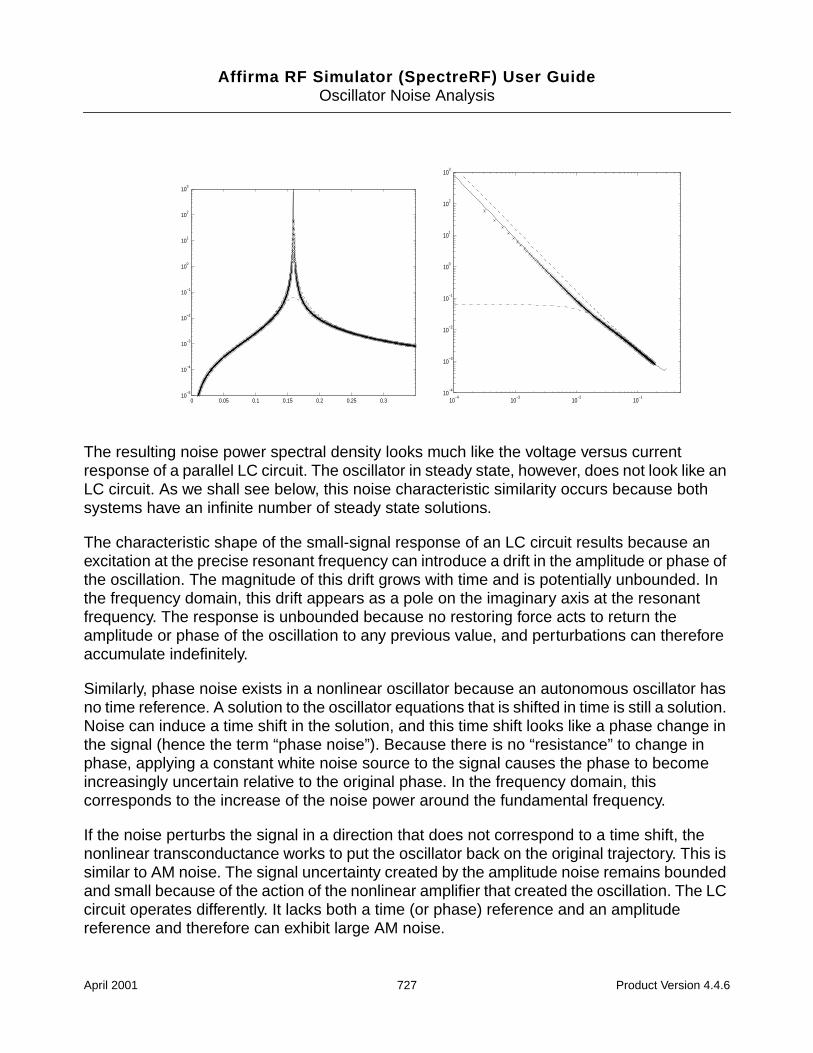
Affirma RF Simulator (SpectreRF) User GuideOscillator Noise Analysis
The resulting noise power spectral density looks much like the voltage versus currentresponse of a parallel LC circuit. The oscillator in steady state, however, does not look like anLC circuit. As we shall see below, this noise characteristic similarity occurs because bothsystems have an infinite number of steady state solutions.
The characteristic shape of the small-signal response of an LC circuit results because anexcitation at the precise resonant frequency can introduce a drift in the amplitude or phase ofthe oscillation. The magnitude of this drift grows with time and is potentially unbounded. Inthe frequency domain, this drift appears as a pole on the imaginary axis at the resonantfrequency. The response is unbounded because no restoring force acts to return theamplitude or phase of the oscillation to any previous value, and perturbations can thereforeaccumulate indefinitely.
Similarly, phase noise exists in a nonlinear oscillator because an autonomous oscillator hasno time reference. A solution to the oscillator equations that is shifted in time is still a solution.Noise can induce a time shift in the solution, and this time shift looks like a phase change inthe signal (hence the term “phase noise”). Because there is no “resistance” to change inphase, applying a constant white noise source to the signal causes the phase to becomeincreasingly uncertain relative to the original phase. In the frequency domain, thiscorresponds to the increase of the noise power around the fundamental frequency.
If the noise perturbs the signal in a direction that does not correspond to a time shift, thenonlinear transconductance works to put the oscillator back on the original trajectory. This issimilar to AM noise. The signal uncertainty created by the amplitude noise remains boundedand small because of the action of the nonlinear amplifier that created the oscillation. The LCcircuit operates differently. It lacks both a time (or phase) reference and an amplitudereference and therefore can exhibit large AM noise.
0 0.05 0.1 0.15 0.2 0.25 0.310
−5
10−4
10−3
10−2
10−1
100
101
102
103
10−4
10−3
10−2
10−1
10−4
10−3
10−2
10−1
100
101
102
103
April 2001 727 Product Version 4.4.6
Affirma RF Simulator (SpectreRF) User GuideOscillator Noise Analysis
Another explanation of the similarity between the oscillator and the LC circuit is that both arelinear systems that have poles on the imaginary axis at the fundamental frequency ω0, thatis, at the complex frequencies s = i ω0. However, the associated transfer functions are notthe same. In fact, because of the time-varying nature of the oscillator circuit, multiple transferfunctions must be considered in the linear time-varying analysis.
Understanding the qualitative behavior of linear and nonlinear oscillators is the first steptowards a complete understanding of oscillator noise behavior. Further understandingrequires more quantitative comparisons that are presented in the next section. Readersuninterested in these mathematical details might wish to skip ahead to “Calculating PhaseNoise” on page 737.
Models for Phase Noise
This section considers several possible models for noise in oscillators. In the engineeringliterature, the most widespread model for phase noise is the Leeson model [leeson]. Thisheuristic model is based on qualitative arguments about the nature of noise processes inoscillators. It shares some properties with the LC circuit models presented in the previoussection. These models fit well with an intuitive understanding of oscillators as resonant RLCcircuits with a feedback amplifier. In the simplest treatment, the amplifier is considered to bea negative conductance whose value is chosen to cancel any positive real impedance in theresonant tank circuit. The resulting linear time-invariant noise model is easy to analyze.
Linear Time-Invariant (LTI) Models
To calculate the noise in a parallel RLC configuration, the noise of the resistor is modeled asa parallel current source of power density . In general, if current noise excitesa linear time-invariant system, then the noise power density produced in a voltage variable isgiven by [gardner].
where H(w) is the transfer function of the LTI transformation from the noise current source“input” to the voltage “output.” The transfer function is defined in the standard way to be
S ω( ) 4kBT R⁄=
Sv ω( ) H ω( ) 2Si ω( )=
H ω( )ν0 ω( )is ω( )---------------=
April 2001 728 Product Version 4.4.6
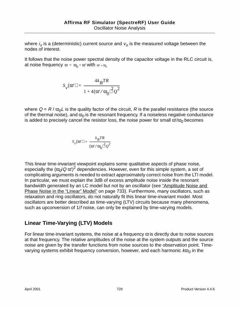
Affirma RF Simulator (SpectreRF) User GuideOscillator Noise Analysis
where is is a (deterministic) current source and vo is the measured voltage between thenodes of interest.
It follows that the noise power spectral density of the capacitor voltage in the RLC circuit is,at noise frequency with
where Q = R / ω0L is the quality factor of the circuit, R is the parallel resistance (the sourceof the thermal noise), and ω0 is the resonant frequency. If a noiseless negative conductanceis added to precisely cancel the resistor loss, the noise power for small ω’/ω0 becomes
This linear time-invariant viewpoint explains some qualitative aspects of phase noise,especially the (ω0/Q ω’)2 dependencies. However, even for this simple system, a set ofcomplicating arguments is needed to extract approximately correct noise from the LTI model.In particular, we must explain the 3dB of excess amplitude noise inside the resonantbandwidth generated by an LC model but not by an oscillator (see “Amplitude Noise andPhase Noise in the “Linear” Model” on page 733). Furthermore, many oscillators, such asrelaxation and ring oscillators, do not naturally fit this linear time-invariant model. Mostoscillators are better described as time-varying (LTV) circuits because many phenomena,such as upconversion of 1/f noise, can only be explained by time-varying models.
Linear Time-Varying (LTV) Models
For linear time-invariant systems, the noise at a frequency ω is directly due to noise sourcesat that frequency. The relative amplitudes of the noise at the system outputs and the sourcenoise are given by the transfer functions from noise sources to the observation point. Time-varying systems exhibit frequency conversion, however, and each harmonic kω0 in the
ω ω0 ω′+= ω′ ω0«
Sv ω′( )4kBTR
1 4 ω′ ω0⁄( )2Q2
+----------------------------------------------=
Sv ω′( )kBTR
ω′ ω0⁄( )2Q2
--------------------------------=
April 2001 729 Product Version 4.4.6
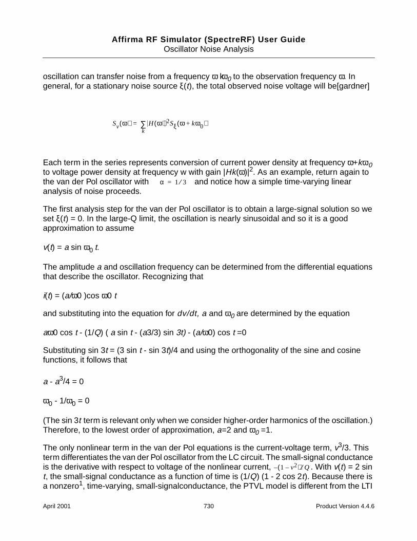
Affirma RF Simulator (SpectreRF) User GuideOscillator Noise Analysis
oscillation can transfer noise from a frequency ω kω0 to the observation frequency ω. Ingeneral, for a stationary noise source ξ(t), the total observed noise voltage will be[gardner]
Each term in the series represents conversion of current power density at frequency ω+kω0to voltage power density at frequency w with gain |Hk(ω)|2. As an example, return again tothe van der Pol oscillator with and notice how a simple time-varying linearanalysis of noise proceeds.
The first analysis step for the van der Pol oscillator is to obtain a large-signal solution so weset ξ(t) = 0. In the large-Q limit, the oscillation is nearly sinusoidal and so it is a goodapproximation to assume
v(t) = a sin ω0 t.
The amplitude a and oscillation frequency can be determined from the differential equationsthat describe the oscillator. Recognizing that
i(t) = (a/ω0 )cos ω0 t
and substituting into the equation for dv/dt, a and ω0 are determined by the equation
aω0 cos t - (1/Q) ( a sin t - (a3/3) sin 3t) - (a/ω0) cos t =0
Substituting sin 3t = (3 sin t - sin 3t)/4 and using the orthogonality of the sine and cosinefunctions, it follows that
a - a3/4 = 0
ω0 - 1/ω0 = 0
(The sin 3t term is relevant only when we consider higher-order harmonics of the oscillation.)Therefore, to the lowest order of approximation, a=2 and ω0 =1.
The only nonlinear term in the van der Pol equations is the current-voltage term, v3/3. Thisterm differentiates the van der Pol oscillator from the LC circuit. The small-signal conductanceis the derivative with respect to voltage of the nonlinear current, . With v(t) = 2 sint, the small-signal conductance as a function of time is (1/Q) (1 - 2 cos 2t). Because there isa nonzero1, time-varying, small-signalconductance, the PTVL model is different from the LTI
Sv ω( ) H ω( )k∑ 2Sξ ω kω0+( )=
α 1 3⁄=
1 v2–( ) Q⁄–
April 2001 730 Product Version 4.4.6
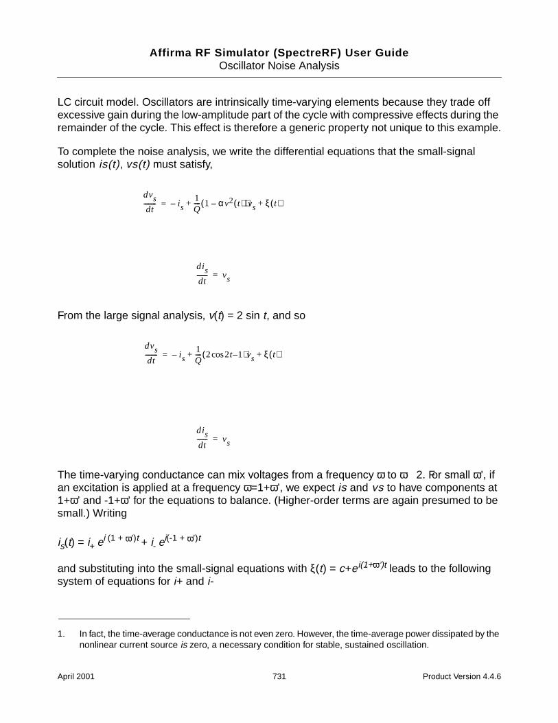
Affirma RF Simulator (SpectreRF) User GuideOscillator Noise Analysis
LC circuit model. Oscillators are intrinsically time-varying elements because they trade offexcessive gain during the low-amplitude part of the cycle with compressive effects during theremainder of the cycle. This effect is therefore a generic property not unique to this example.
To complete the noise analysis, we write the differential equations that the small-signalsolution is(t), vs(t) must satisfy,
From the large signal analysis, v(t) = 2 sin t, and so
The time-varying conductance can mix voltages from a frequency ω to ω 2. For small ω’, ifan excitation is applied at a frequency ω=1+ω’, we expect is and vs to have components at1+ω’ and -1+ω’ for the equations to balance. (Higher-order terms are again presumed to besmall.) Writing
is(t) = i+ ei (1 + ω’)t + i- ei(-1 + ω’)t
and substituting into the small-signal equations with ξ(t) = c+ei(1+ω’)t leads to the followingsystem of equations for i+ and i-
1. In fact, the time-average conductance is not even zero. However, the time-average power dissipated by thenonlinear current source is zero, a necessary condition for stable, sustained oscillation.
dvsdt
-------- is–1Q---- 1 αv2 t( )–( )vs ξ t( )+ +=
disdt------- vs=
dvsdt
-------- is–1Q---- 2 2t 1–cos( )vs ξ t( )+ +=
disdt------- vs=
April 2001 731 Product Version 4.4.6
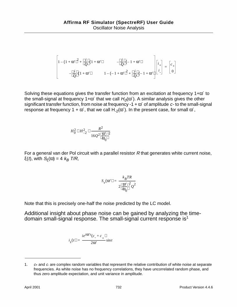
Affirma RF Simulator (SpectreRF) User GuideOscillator Noise Analysis
Solving these equations gives the transfer function from an excitation at frequency 1+ω´ tothe small-signal at frequency 1+ω´ that we call H0(ω´). A similar analysis gives the othersignificant transfer function, from noise at frequency -1 + ω´ of amplitude c- to the small-signalresponse at frequency 1 + ω´, that we call H-2(ω´). In the present case, for small ω´,
For a general van der Pol circuit with a parallel resistor R that generates white current noise,ξ(t), with Sξ(ω) = 4 kB T/R,
Note that this is precisely one-half the noise predicted by the LC model.
Additional insight about phase noise can be gained by analyzing the time-domain small-signal response. The small-signal current response is1
1. c+ and c- are complex random variables that represent the relative contribution of white noise at separatefrequencies. As white noise has no frequency correlations, they have uncorrelated random phase, andthus zero amplitude expectation, and unit variance in amplitude.
1 1 ω′+( )2–iQ----
1 ω′+( )+iQ----
1– ω′+( )–
iQ----
1 ω′+( )– 1 1– ω′+( )2 iQ----
1– ω′+( )+–
i+i -
c+
0=
H02 H 2–
2 R2
16Q2 ω′ω0-------
2-----------------------------≅ ≅
Sv ω′( )kBTR
2ω′ω0-------
2Q
2--------------------------=
is t( )ieiω′t c- c+
+( )
2ω′------------------------------------ tsin=
April 2001 732 Product Version 4.4.6
Affirma RF Simulator (SpectreRF) User GuideOscillator Noise Analysis
Notice that because the large-signal current is i(t) = 2 cos t, and the sine and cosine functionsare orthogonal, the total noise for small ω´ that we computed is essentially all phase noise.
Amplitude Noise and Phase Noise in the “Linear ” Model
Occasional claims are made that in oscillators “half the noise is phase noise and half thenoise is amplitude noise.” However, as the simple time-varying analysis above shows, in aphysical oscillator the noise process is mostly phase noise for frequencies near thefundamental. It is true that in an LC-circuit half the total noise power corresponds to AM-likemodulation, and the other half, to phase modulation. In the literature, the AM part of the noiseis sometimes disregarded when quoting the oscillator noise although this is not always thecase. (The SpectreRF circuit simulator computes the total noise generated by the circuit; see“Details of the SpectreRF Calculation” on page 734).
However, a “linear” oscillator does not really exist. Physical oscillators operate with a tradeoffof gain that causes growing signal strength and nonlinear compressive effects that act to limitthe signal amplitude. For noise calculation, the oscillator cannot be considered a linear time-invariant system because there are intrinsic nonlinear effects that produce large phase noisebut limited amplitude noise. Oscillators are time-varying, and they therefore require a time-varying small-signal analysis.
Arguments that start with stationary white noise and pass it through a linear model in aforward-analysis fashion produce incorrect answers. This is true because they neglect thetime-variation of the conductances (and possibly the capacitances) in the circuit. In the simplecases considered here, the conductances vary in time in a special way so as to produce noamplitude noise, only phase noise.
They have that special variation because they result from linearization about an oscillator limitcycle. An oscillator in a limit cycle has a large response to phase perturbations, but not toamplitude perturbations. The amplitude perturbations are limited by the properties of thenonlinear amplifier, but the phase perturbations can persist. Spectre simulation calculates thecorrect phase noise because it “knows” about the oscillator properties.
Similarly, arguments (for example, the book by Robins) that start with noise power and derivephase noise in a backwards fashion also usually produce incorrect results because theycannot correctly account for frequency correlations in the noise of the oscillator. Thesefrequency correlations are introduced by the time-varying nature of the circuit.
Occasionally, a netlist appears in which a negative resistance precisely cancels a positiveresistance to create a pure LC circuit. Because such a circuit has an infinite number ofoscillation modes,1 The SpectreRF circuit simulator cannot correctly calculate the noisebecause it assumes a unique oscillation. Such a circuit is not physically realizable becauseadding or subtracting a microscopically small amount of conductance makes the circuit either
April 2001 733 Product Version 4.4.6
Affirma RF Simulator (SpectreRF) User GuideOscillator Noise Analysis
go into nonlinear operation (amplifier saturation) or become a damped LC circuit that has aunique final equilibrium point. This equilibrium point is the zero-state solution. Trying to createthe negative resistance oscillator is like trying to bias a circuit on a metastable point.
Details of the SpectreRF Calculation
This section contains the mathematical details of how the SpectreRF circuit simulatorcomputes noise in oscillators. Understanding the material in this section can help youtroubleshoot and understand difficult oscillator problems.
The analysis Spectre performs is similar to the simple analysis in the section “Linear Time-Varying (LTV) Models” on page 729. Spectre first finds the periodic steady state of theoscillator using the PSS analysis and then linearizes around this trajectory. The resultingtime-varying linear system is used to calculate the noise power density. The primarydifference between the SpectreRF calculation and the previous analysis is that the basisfunctions used for the SpectreRF calculation are not a just few sinusoids, but rather acollection of many piecewise polynomials. The use of piecewise polynomials allows Spectresimulation to solve circuits with arbitrary waveforms, including highly nonlinear circuitbehavior.
Noise computations are usually performed with a small-signal assumption, but a rigoroussmall-signal characterization of phase noise is complicated because the variance in thephase of the oscillation grows unbounded over time. From a mathematical viewpoint, anoscillator is an autonomous system of differential equations with a stable limit cycle. Anoscillator has phase noise because it is neutrally stable with respect to noise perturbationsthat move the oscillator in the direction of the limit cycle. Such “phase” perturbations persistwith time, whereas transverse fluctuations are damped with a characteristic time inverselyproportional to the quality factor of the oscillator.
Further care is necessary because, in general, the two types of excitations (those that createphase slippage and those responsible for time-damped fluctuations) are not strictly those thatare parallel or perpendicular, respectively, to the oscillator trajectory, as is sometimes claimed(for example, in [hajimiri]).
However, one must realize that the noise powers at frequencies near the fundamentalfrequency correspond to correlations between points that are widely separated on theoscillator envelope. In other words, they are long-time signal effects. In fact, asymptotically(at long times), the ratio of the variance of any state variable to its power at the fundamentalfrequency is unity for any magnitude of the noise excitation. Therefore, in practical cases, wecan consider only small deviations in the state variables when describing the phase noise.
1. Any amplitude oscillation can exist, depending on the initial conditions, as long as the amplitude is lessthan the amplifier saturation point.
April 2001 734 Product Version 4.4.6
Affirma RF Simulator (SpectreRF) User GuideOscillator Noise Analysis
The first step in the noise analysis is to determine the oscillator steady state solution. This isdone in the time domain using shooting methods [telichevesky95]. Once the periodic steady-state is obtained, the circuit equations are linearized around that waveform in order to performthe small-signal analysis.
The time-varying linear system describing the small-signal response vs(t) of the oscillator toa signal w(t) can be written in general form as [telichevesky96, okumura]]
where C(t) and G(t) represent the linear, small-signal, time-varying capacitance andconductance matrices, respectively. These matrices are obtained by linearization about theperiodic steady state solution (the limit cycle). To understand the nature of time-varying linearanalysis, we introduce the concept of Floquet multipliers.
Suppose x(t) is a solution to the oscillator circuit equations that is periodic with period T. Ifx(0) is a point on the periodic solution xL(t), then x(T) = x(0). If x(0) is perturbed slightly offthe periodic trajectory, x(0) = xL(0) + δ x, then x(T) is also perturbed, and in general for smallδx,
The Jacobian matrix x(T)/ x(0)is called the sensitivity matrix. The SpectreRF circuitsimulator uses an implicit representation of this matrix both in the shooting-method thatcalculates the steady state and in the small-signal analyses. To see how the sensitivity matrixrelates to oscillator noise analysis, consider the effect of a perturbation at time t=0 severalperiods later, at t = nT. From the above equation,
C t( ) ddt----- G t( )+ vs L t( )vs t( )≡ w t( )=
x T( ) xL T( ) x T( )∂x 0( )∂
--------------δx≈–
x nT( ) xL nT( ) x T( )∂x 0( )∂
--------------n
δx≈–
April 2001 735 Product Version 4.4.6
Affirma RF Simulator (SpectreRF) User GuideOscillator Noise Analysis
so
where φι is an eigenvector of the sensitivity matrix. The Ci are the expansion coefficients ofδx in the basis of φι . If ψi is a left eigenvector of the sensitivity matrix, then1
Let λ be an eigenvalue of the sensitivity matrix. In the context of linear time-varying systems,the eigenvalues λ are called Floquet multipliers. If all the λ have magnitude less than one(corresponding to left-half-plane poles), the perturbation decays with time and the periodictrajectory is stable. If any λ has a magnitude greater than one, the oscillation cannot belinearly stable because small perturbations soon force the system away from the periodictrajectory xL(t). A stable nonlinear physical oscillator, however, must be neutrally stable withrespect to perturbations that move it in the direction of the orbit2. This is true because a time-shifted version of the oscillator periodic trajectory still satisfies the oscillator equations. Inother words, one of the Floquet multipliers must be equal to unity. This Floquet multiplier isresponsible for phase noise in the oscillator. The associated eigenvector determines thenature of the noise.
If λ = eη is a Floquet multiplier, then η + i k ω0 is a pole of the time-varying linear system forany integer k. Therefore, because of the unity Floquet multiplier, the time-varying linearsystem has poles on the imaginary axis at k ω0. This is very similar to what occurs in a pureLC resonator, and it explains the identical shape of the noise profiles.
Because operator L(t) has poles at the harmonics of the oscillation frequency, numericalcalculations of the noise at nearby frequencies become inaccurate if treated in a naivemanner [anzill,kaertner92]. To correctly account for the phase noise, the SpectreRF circuitsimulator finds and extracts the eigenvector that corresponds to the unity Floquet multiplier.To correctly extract the phase noise component, both the right and left eigenvectors arerequired. Once these vectors are obtained, the singular (phase noise) contribution to thenoise can be extracted. The remaining part of the noise can be obtained using the usualiterative solution techniques [telichevesky96] in a numerically well-conditioned operation.
1. A left eigenvector of a matrix is an eigenvector of its transpose.
2. These are not necessarily perturbation in the direction of the orbit because, in general, y ≠ φι !
x nT( ) xL nT( )– Ciλinφi
i∑≈
Ci ψiT= δx
April 2001 736 Product Version 4.4.6
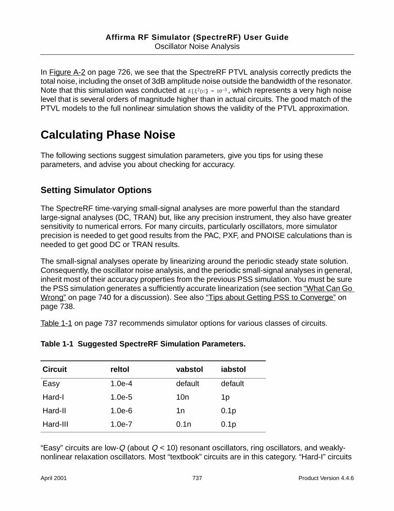
Affirma RF Simulator (SpectreRF) User GuideOscillator Noise Analysis
In Figure A-2 on page 726, we see that the SpectreRF PTVL analysis correctly predicts thetotal noise, including the onset of 3dB amplitude noise outside the bandwidth of the resonator.Note that this simulation was conducted at , which represents a very high noiselevel that is several orders of magnitude higher than in actual circuits. The good match of thePTVL models to the full nonlinear simulation shows the validity of the PTVL approximation.
Calculating Phase Noise
The following sections suggest simulation parameters, give you tips for using theseparameters, and advise you about checking for accuracy.
Setting Simulator Options
The SpectreRF time-varying small-signal analyses are more powerful than the standardlarge-signal analyses (DC, TRAN) but, like any precision instrument, they also have greatersensitivity to numerical errors. For many circuits, particularly oscillators, more simulatorprecision is needed to get good results from the PAC, PXF, and PNOISE calculations than isneeded to get good DC or TRAN results.
The small-signal analyses operate by linearizing around the periodic steady state solution.Consequently, the oscillator noise analysis, and the periodic small-signal analyses in general,inherit most of their accuracy properties from the previous PSS simulation. You must be surethe PSS simulation generates a sufficiently accurate linearization (see section “What Can GoWrong” on page 740 for a discussion). See also “Tips about Getting PSS to Converge” onpage 738.
Table 1-1 on page 737 recommends simulator options for various classes of circuits.
Table 1-1 Suggested SpectreRF Simulation Parameters.
“Easy” circuits are low-Q (about Q < 10) resonant oscillators, ring oscillators, and weakly-nonlinear relaxation oscillators. Most “textbook” circuits are in this category. “Hard-I” circuits
Circuit reltol vabstol iabstol
Easy 1.0e-4 default default
Hard-I 1.0e-5 10n 1p
Hard-II 1.0e-6 1n 0.1p
Hard-III 1.0e-7 0.1n 0.1p
E ξ2 t( ) 10 3–=
April 2001 737 Product Version 4.4.6
Affirma RF Simulator (SpectreRF) User GuideOscillator Noise Analysis
are most other resonant oscillators; circuits with complicated AGC, load, or bias circuitry; andrelaxation or ring oscillators that exhibit moderate to strong nonlinear or “stiff” effects. This isthe best general-purpose set of options.
A few particularly difficult circuits might need to be classified as “Hard-II” or even “Hard-III”.Usually these options are used only in a convergence study (see “How to Tell If the AnswerIs Correct” on page 739) or for circuits that previously failed a conversion study using lessstrict options. Circuits in this category often exhibit some form of unusual behavior (see “WhatCan Go Wrong” on page 740). Sometimes this behavior results from circuit properties (forexample, some very high-Q crystal oscillators and some very stiff relaxation oscillatorcircuits). Occasionally, the behavior reflects a design flaw.
Usually setting method=gear2only is recommended for the PSS simulation (but see “WhatCan Go Wrong” on page 740).
Tips about Getting PSS to Converge
Most circuits can be converged by manipulating the parameters tstab and steadyratio. Settstab large enough so that the oscillation amplitude increases to near its steady state valueand most of the other transients have died out. You can estimate the value of tstab either byperforming a tran analysis, or by performing a PSS analysis itself with the settingsaveinit=yes. At tighter simulation tolerances, if steadyratio is too small, the PSS simulationoften does not converge. Setting steadyratio=0.1 usually fixes this problem.
For particularly difficult circuits, or for large circuits that make the above procedureexcessively time-consuming, you can use a slightly different procedure.
Try the options settings reltol=1e-3 and steadyratio=1, and run the PSS analysis with a verylong tstab parameter setting. Relaxing iabstol and vabstol might also be necessary. Savethis solution to a file using the writefinal option. This step can usually obtain a low-accuracyPSS solution with an acceptable simulation time. Using a very long tstab increases theprobability that the simulation converges, and relaxing reltol ensures a reasonable simulationtime and increases the probability of PSS convergence.
For some circuits, the oscillation might die out before the oscillator builds up a final level, orthe circuit might oscillate for a while before returning to a zero-state. Setting saveinit=yes letsyou view the initial transient waveforms to determine if this problem is occurring. This problemmight be caused by difficulty starting the oscillator, or it might be the result of artificialnumerical losses introduced by the very large timesteps. This last cause is likely if the PSSoptions method parameter was set to gear2only, gear2, or euler. In these cases, decreasereltol or set the maxstep parameter to make the simulator use smaller step sizes.
April 2001 738 Product Version 4.4.6
Affirma RF Simulator (SpectreRF) User GuideOscillator Noise Analysis
Once the initial PSS simulation is completed, reset the accuracy parameters reltol, vabstol,and iabstol to their preferred final values. Then rerun the PSS simulation using the readicoption to read in the initial conditions saved from the first, low-accuracy, PSS run. You mightneed to leave the steadyratio setting in the 0.1 to 1 range to achieve convergence. Any valueof steadyratio less than one or so should be acceptable.
If the circuit contains independent sources used to start the oscillator, set the PSS start timeto a large enough value to be sure these sources are all inactive at the start of the simulation.
You need not use a large tstab value in this second step. However, varying tstab slightly inthis second analysis can sometimes help secure convergence.
Some users report that decreasing the maximum allowed timestep sometimes helpsconvergence. To do this, either decrease the maxstep parameter or increase the maxacfreqparameter.
How to Tell If the Answer Is Correct
To be sure that only small numerical errors are introduced into the phase noise calculation,you can simulate the oscillator with progressively more stringent accuracy parameters untilthe change in the calculated noise is less than the desired simulation precision. Such a setof simulations typically starts from the “Easy” parameter set given in Table 1-1 on page 737and proceeds downward through the table until the calculated noise no longer changes.Remember that generally all three tolerances must be lowered to ensure that the discreteapproximations used by the Spectre simulator are converging to the continuous solutions ofthe physical circuit.
Using the final solutions from the previous simulations as an initial estimate for the next PSSsimulations can help minimize the total PSS simulation time. Use the writefinal parameter inPSS to write out each final PSS solution and the readic parameter to read it back in.
Changing the tstab parameter can sometimes identify problem circuits or simulations (see“The tstab Parameter” on page 743 for details).
Troubleshooting Phase Noise Calculations
The SpectreRF circuit simulator calculates noise effectively for most oscillators. However,circuits that are very “stiff”,1 very nonlinear, or just poorly designed, can occasionally cause
1. “Stiff” circuits exhibit dynamics with two or more very different time scales, for example, a relaxation oscil-lator with a square-wave-like periodic oscillation. Over most of the cycle, the voltages change very slowly,but occasional rapid transitions are present.
April 2001 739 Product Version 4.4.6
Affirma RF Simulator (SpectreRF) User GuideOscillator Noise Analysis
the simulator problems. This section describes some of the reasons for the problems, whatgoes wrong, how to identify problems, and how to fix them.
Reading “Details of the SpectreRF Calculation” on page 734 is often helpful fortroubleshooting particularly difficult circuits.
Known Limitations of the Simulator
Any circuit that does not have a stable periodic steady state cannot be analyzed by theSpectreRF circuit simulator because oscillator noise analysis is performed by linearizingaround a waveform that is assumed to be strictly periodic.
For example, oscillators based on IMPATT diodes generate strong subharmonic responsesand cannot be properly analyzed with the SpectreRF circuit simulator. As another example,Colpitts oscillators, properly constructed, can be made to exhibit chaotic as well assubharmonic behavior.
Similarly, any circuit with significant large-signal response at tones other than thefundamental and its harmonics might create problems for the simulator. Some types ofvaractor-diode circuits might fit this category. In addition, some types of AGC circuitry and, onoccasion, bias circuitry can create these effects.
The SpectreRF circuit simulator cannot simulate these circuits because simulation of anautonomous circuit with subharmonic or other aperiodic components in the large signalresponse essentially requires foreknowledge of which frequency components are important.Such foreknowledge requires Fourier analysis of very long transient simulations and cannotbe easily automated. Such simulations can be very expensive in any event.
What Can Go Wrong
Generic PSS simulation problems
Any difficulties in the underlying PSS analysis affect the phase noise computation. Forexample, underestimating the oscillator period or failing to start the oscillator properlycan cause PSS convergence problems that make running a subsequent PNOISEanalysis impossible.
Hypersensitive circuits
Occasionally, we see circuits that are extremely sensitive to small parameter changes.Such a circuit was a varactor-tuned VCO that had the varactor bias current, and thereforethe oscillation frequency, set by a 1TΩ resistor. Changing the resistor to 2TΩ, which is a1e-12 relative perturbation in the circuit matrices, changed the oscillation frequency from125MHz to 101Mhz. We believe that such extreme circuit sensitivity results in PSS
April 2001 740 Product Version 4.4.6
Affirma RF Simulator (SpectreRF) User GuideOscillator Noise Analysis
simulations that are very imprecise. In particular, the calculated periods have relativelylarge variations. If precise PSS simulations areimpossible, precise noise calculations are also impossible.
In such a case, you must fix the circuit.
Subharmonics or parametric oscillator modulation
Sometimes bias and AGC circuitry create small-amplitude parasitic oscillations in thelarge signal waveform. You can identify these oscillations by performing a transientsimulation to steady-state and then looking for modulation of the envelope of theoscillation waveform. (For high-Q circuits and/or low-frequency parasitics, this transientsimulation might be very lengthy.)
In this case, because the oscillator waveform is not actually periodic, the PSS simulationcan only converge to within approximately the amplitude of the parasitic oscillation. If thewaveform possesses a parasitic oscillation that changes amplitude, over one period,around 10-5 relative to the oscillator envelope, then convergence with reltol < 10-5 isprobably not possible (assuming steadyratio is one or less).
These effects might also appear as a parametric sideband amplification phenomenon(see “Frequently Asked Questions” on page 744).
Small-signal frequency much higher than fundamental frequency
The same timesteps are used for both the small-signal analysis and the PSS analysis. Ifthe small-signal frequency is much higher than the fundamental frequency, much smallertimesteps might be required to resolve the small signal accurately than are needed forthe large signal. To force Spectre simulation to take sufficiently small timesteps in thePSS simulation, be sure the maxacfreq parameter is set correctly.
Wide timestep variation
Occasionally, in simulations that generate PSS waveforms with timesteps that vary overseveral orders of magnitude, the linear systems of equations that determine the small-signal response become ill-conditioned. As a result, the noise analysis is inaccurate.Usually this occurs because excessive simulator precision has been requested, forexample, nine-digit precision. Using method=traponly in the PSS solution is sometimeshelpful in eliminating the problem. Another solution is to set maxstep to a very smallvalue in the PSS analysis or to specify a very large maxacfreq value.
Device model problems
The noise calculations are usually inaccurate if the device models leave their physicallymeaningful operating range during the large-signal PSS solution.
Similarly, if the models are discontinuous, or have discontinuous derivatives, the small-signal analysis might be inaccurate.
April 2001 741 Product Version 4.4.6
Affirma RF Simulator (SpectreRF) User GuideOscillator Noise Analysis
Problems resolving Floquet multipliers in stiff relaxation oscillators
Sometimes in very stiff relaxation oscillators, the PSS solution rapidly and easilyconverges; but the numerically calculated Floquet multiplier associated with the PSSsolution is far from unity. Typically, this multiplier is real and has a magnitude much largerthan unity. The SpectreRF circuit simulator prints a warning (Message III, below). It isinteresting that sometimes the phase noise is quite accurate even with low simulationtolerances. If you have this problem, perform a convergence study (see “How to Tell If theAnswer Is Correct” on page 739).
Problems resolving Floquet multipliers in high-Q resonant circuits
In a physical oscillator, there is one Floquet multiplier equal to unity. In an infinite-Q linearresonator, however, the multipliers occur in complex conjugate pairs. A very high-Qnonlinear oscillator has another Floquet multiplier on the real axis nearly equal to, butslightly less than, one. In this presence of numerical error, however, these two realFloquet multipliers can appear as a complex-conjugate pair to the simulator. The phasenoise is computed using the Floquet vector associated with the unity Floquet multiplier.When the two multipliers appear as a complex pair, the relevant vector is undefined.When Spectre can correctly identify this situation, it prints a warning (Message III,below). The solution is usually to simulate using the next higher accuracy step (seeTable 1-1 on page 737) Sometimes varying tstab can also help with this problem.
If the circuit is really an infinite-Q resonator (for example, a pure parallel LC circuit), themultipliers always appear as complex conjugate pairs and the noise computations arenot accurate close to the fundamental frequency. Such circuits are not physicaloscillators, and Spectre is not designed to deal with them; see “Amplitude Noise andPhase Noise in the “Linear” Model” on page 733 and “Frequently Asked Questions” onpage 744.
Phase Noise Error Messages
SpectreRF originates error messages when it encounters several types of known numericaldifficulty. To interpret the error messages produced by the phase noise analysis, you mustknow the material in the section “Details of the SpectreRF Calculation” on page 734.
Message I: “The Floquet eigenspace computed by spectre PSS analysis appearsto be inaccurate. PNOISE computations may be inaccurate. Consider re-runningthe simulation with smaller reltol and method=gear2only.”
The eigenvector responsible for phase noise was inaccurately computed, and the PSSsimulation tolerances are possibly too loose. Try simulating the circuit at the next higheraccuracy setting (see Table 1-1 on page 737) and then compare the calculated noise in thetwo simulations.
April 2001 742 Product Version 4.4.6
Affirma RF Simulator (SpectreRF) User GuideOscillator Noise Analysis
Message II: “The Floquet eigenspace computed by spectre PSS analysis appearsto be ill-defined. PNOISE computations may be inaccurate. Consider re-runningthe simulation with smaller reltol , different tstab (s), and method=gear2only .Check the circuit for unusual components.”
This can be an accuracy problem, or it can result from an unusual circuit topology orsensitivity. Tighten the accuracy requirements (see Table 1-1 on page 737) as much aspossible. If this message appears in all the simulations, the noise is possibly incorrect even ifthe simulations agree.
Message III: “The Floquet eigenspace computed by spectre PSS analysis appearsto be inaccurate and/or the oscillator possesses more than one stable mode ofoscillation. PNOISE computations may be inaccurate. Consider re-running thesimulation with smaller reltol, different tstab (s), and method=gear2only. "
All the real Floquet multipliers were well-separated from unity, suggesting that the PSSsimulation tolerances might be too loose. Simulate the circuit at the next higher accuracysetting (see Table 1-1 on page 737) and then compare the calculated noise in the twosimulations. If the calculated noise does not change, it is probably correct even if thismessage appears in both simulations.
The tstab Parameter
Because SpectreRF performs the PSS calculation in the time domain by using a shootingmethod, an infinite number of possible PSS solutions exist, depending on where the firsttimepoint of the PSS solution is placed relative to the oscillator phase.
The placement of the first timepoint is determined by the length of the initial transientsimulation, which you can control using the tstab parameter. If the tstab value causes theedges of the periodic window to fall on a point where the periodic oscillator waveform ismaking very rapid transitions, it will probably be very difficult for PSS to converge. Similarly,the small-signal analyses probably are not very accurate. Avoid such situations. If the start ofthe PSS waveform falls on a very fast signal transition, you usually need to view the resultsof further small-signal analyses with some scepticism.
Although a poor choice of the tstab parameter value can degrade convergence and accuracy,appropriate use of tstab can help to identify problem circuits and to estimate the reliability oftheir noise computations.
If you perform several PSS and Pnoise computations that differ only in their tstab parametervalues, the results should be fairly similar, within a relative deviation of the same order ofmagnitude as the simulator parameter reltol. If this is not the case, you might not have setthe simulator accuracy parameters tight enough to achieve an accurate solution; and you
April 2001 743 Product Version 4.4.6
Affirma RF Simulator (SpectreRF) User GuideOscillator Noise Analysis
need to reset one or more of the parameters reltol, vabstol, or iabstol. The circuit might alsobe poorly designed and very sensitive to perturbations in its parameters.
If the calculated fundamental period of the oscillator varies with tstab even when you setreltol, iabstol, and vabstol to very small (but not vanishingly small) values, the circuit isprobably poorly designed, exhibiting anomalous behavior, or both. (see section “KnownLimitations of the Simulator” on page 740).
Frequently Asked Questions
1. Does SpectreRF simulation calculate phase noise, amplitude noise, or both?
SpectreRF simulation computes the total noise of the circuit, both amplitude and phasenoise. What the Affirma analog circuit design environment plots as “phase noise” is reallythe total noise scaled by the power in the fundamental oscillation mode. Close enoughto the fundamental frequency, the noise is all phase noise, so what the designenvironment plots of “phase noise” are really the phase noise as long as it is a good waysabove the noise floor.
Some discussions of oscillator noise based on a simple resonator/amplifier descriptiondescribe the total noise, at small frequency offsets from the fundamental, as being halfamplitude noise and half phase noise. In reality, for physical oscillators, near thefundamental nearly all the noise is phase noise. Therefore, these simple modelsoverestimate the total noise by 3dB. For a detailed explanation, see the phase noisetheory section, “Details of the SpectreRF Calculation” on page 734 and the detaileddiscussion of the van der Pol oscillator, “Linear Time-Varying (LTV) Models” onpage 729.
2. I have a circuit that contains an oscillator. Can I simulate the oscillatorseparately and use the phase noise Spectre calculates as input for a secondPSS/PNOISE simulation?
No, at least, not at this time. Oscillators generate noise with correlated spectralsidebands. Currently, SpectreRF simulation output represents only the time-averagenoise power, not the correlation information, so the noise cannot be input to a simulationthat contains time-varying elements that might mix together noise from separatefrequencies.
If the second circuit is a linear filter (purely lumped linear time-invariant elements, suchas resistors, capacitors, inductors, or a linearization of a nonlinear circuit around a DCoperating point) that generates no frequency mixing, then you can use the output of theSpectreRF Pnoise analysis as a noisefile for a subsequent NOISE (not Pnoise!)analysis.
3. How accurate are the phase noise calculations? What affects the errors?
April 2001 744 Product Version 4.4.6
Affirma RF Simulator (SpectreRF) User GuideOscillator Noise Analysis
Initially, we must distinguish between modeling error and simulation (numerical) error. Ifthe device models are only good to 10% then the simulation is only good to 10 percent(or worse). So, for the rest of this note, we discuss numerical error introduced by theapproximations in the algorithms.
We must also distinguish between absolute and relative signal frequencies in the noiseanalysis. When the noise frequency is plotted on an absolute scale, the error is primarilya function of the variance in the calculated fundamental period. This is true because ofthe singular behavior, in these regions, of the phase noise near a harmonic of thefundamental. To see this behavior, note that for the simple oscillator driven by whitenoise, the noise power is proportional to the offset from the fundamental frequency,
If a small error is made in the calculation of ω0, the error ∆ Sv in the noise is proportionalto S / ω0, i.e.
This error can be very large even if the error in ω0, ∆ω0, is small. However, because ofthe way SpectreRF simulation extracts out the phase noise, the calculated phase noise,as a function of offset from the fundamental frequency, can be quite accurate even forvery small offsets.
Let us now consider how much error is present in the calculated fundamental frequency.Because the numerical error is related to many simulation variables, it is difficult toquantify, without examination, how much is present. However, as a rough approximation,if we define the quantity
r =min reltol, iabstol/max(i), vabstol/max(v)
where max(i) and max(v) are the maximum values of voltage and current over the PSSperiod, then, under some assumptions, the error d ω0 in the fundamental ω0 probablysatisfies
r ω0 < δ ω0 < M r ω0
Sv ω( ) 1
ω ω0–( )2-------------------------∝
∆Sv ω( )∆ω0
ω ω0–( )3-------------------------∝
April 2001 745 Product Version 4.4.6
Affirma RF Simulator (SpectreRF) User GuideOscillator Noise Analysis
where M is the number of timesteps taken for the PSS solution. This analysis assumesthat steadyratio is sufficiently tight, not much more than one, and also that iabstol andvabstol are sufficiently small.
If a good estimate of the accuracy in the fundamental is required, run the PSS simulationwith many different accuracy settings, initial conditions and/or tstab values (see “How toTell If the Answer Is Correct” on page 739 and “The tstab Parameter” on page 743). Forexample, to estimate how much numerical error remains in the calculated fundamentalfrequency for a given simulation, run the simulation; reduce reltol, iabstol, and vabstolby a factor of 10 to100; rerun the simulation; and then compare the calculatedfundamental frequencies. For the sorts of parameters we recommend for oscillatorsimulations, four to five digits of precision seems typical. As of version 4.4.2, SpectreRFsimulation estimates of the fundamental frequency are unlikely to be accurate to morethan six or seven digits. Past that point, round off error and anomalous effects introducedby vastly varying timesteps offset any gains from tightening the various accuracyparameters.
For phase noise calculations, again it is unrealistic to expect relative precision of betterthan the order of reltol. That is, if reltol is 10-5 and the oscillator fundamental is about 1GHz, the SpectreRF numerical fuzz for the calculated period is probably about 10KHz.Therefore, when plotted on an absolute frequency scale, the phase noise calculationexhibits substantial variance within about 10KHz of the fundamental.
However, when plotted on a frequency scale relative to the fundamental, the phasenoise calculation might be more precise for many oscillators. If the circuit is stronglydissipative (that is, low-Q, such as ring oscillators and relaxation oscillators), the phasenoise calculation is probably fairly accurate up to very close to the fundamentalfrequency even with loose simulation tolerance settings. High-Q circuits are moredemanding of the simulator and require more stringent simulation tolerances to producegood results. In particular, circuits that use varactor diodes as tuning elements in a high-Q tank circuit appear to cause occasional problems. Small modifications to the netlist(runs with different tstab values and minor topology changes) can usually tell youwhether (and where) the simulator results are reliable.
Simulation accuracy is determined by how precisely SpectreRF simulation can solve theaugmented nonlinear boundary value problem that determines the periodic steady state.The accuracy of the BVP solution is controlled primarily by the simulation variablesreltol, iabstol, vabstol, steadyratio, and lteratio. Typically, steadyratio and lteratioare fixed, so reltol is usually the variable of interest.
Accuracy can occasionally be somewhat affected by other variables such as relref,method, number of timesteps, and tstab. Again, the physical properties of the circuit canput limitations on the accuracy.
4. I have a circuit with an oscillator and a sinusoidal source. Can I simulate thiscircuit with SpectreRF simulation?
April 2001 746 Product Version 4.4.6
Affirma RF Simulator (SpectreRF) User GuideOscillator Noise Analysis
In general, SpectreRF simulation is not intended to analyze circuits that containautonomous oscillators and independent periodic sources.
If the circuit contains components that could potentially oscillate autonomously and alsoindependent large-signal sinusoidal sources, SpectreRF simulation works properly onlyif two conditions are fulfilled. The system must be treated as a driven system, and thecoupling from the sinusoidal sources to the oscillator components must be strongenough to lock the oscillator to the independent source frequency. (In different contexts,this is known as "oscillator entrainment" or "phase-locking.") The normal (non-autonomous) PSS and small-signal analyses function normally in these conditions.
If the autonomous and driven portions of the circuit are weakly coupled, the circuitwaveform might be more complicated, for example, a two-tone (quasiperiodic) signalwith incommensurate frequencies. Even if PSS converges, further small signal analyses(PAC, PXF, PNOISE) almost certainly give the wrong answers.
5. What is the significance of total noise power?
First, you must understand that SpectreRF simulation calculates and measures noise involtages and currents. The total power in the phase process is unbounded, but the powerin the actual state variables is bounded.
Oscillator phase noise is usually characterized by the quantity
where P1 is the power in the fundamental component of the steady state solution andSv(f) is the power spectral density of a state variable V. For an oscillator with only whitenoise sources, L(f) has a Lorentizian line shape,
d f( ) Sv f( )P1
--------------=
L f( ) 1π--- a
a2 f 2+------------------=
April 2001 747 Product Version 4.4.6
Affirma RF Simulator (SpectreRF) User GuideOscillator Noise Analysis
where a is dependent on the circuit and noise sources, and thus the total phase noisepower ∫L (f) df = 1. Because
we are led to the uncomfortable, but correct, conclusion that the variance in any variableis 100 percent of the RMS value of the variable, irrespective of circuit properties orthe amplitude of the noise sources.
Physically, this means that if a noise source has been active, sincet = -∞, then the voltage variable in question is randomly distributed over its wholetrajectory. Therefore, the relative variance is one. Clearly, the variance is not a physicallyuseful characterization of the noise, and the total noise power must be interpretedcarefully. What is actually needed is the variance as a function of time, given a fixedreference for the signal in question; or, more often, the rate at which the varianceincreases from a zero point; or, sometimes, the increment in the variance from cycle tocycle. That is, we want to specify the phase of the oscillator signal at a given time pointand to find a statistical characterization of the variances relative to that time. But becauseof the non-causal nature of the Fourier integral, quantities like the total noise power giveus information about the statistical properties of the signal over all time.
6. What’s the story with pure linear oscillators (LC circuits)?
Oddly enough, SpectreRF simulation is not set up to do Pnoise analysis on pure LCcircuits.
Pure LC circuits are not physically realizable oscillators, and the mathematics thatdescribes them is different from the mathematics that describes physical oscillators. Aspecial option must be added to the code in order for Pnoise to handle “linear oscillators.”See “Models for Phase Noise” on page 728, and, in particular, “Amplitude Noise andPhase Noise in the “Linear” Model” on page 733. Because the normal NOISE analysisis satisfactory for these circuits and also much faster, it is unlikely that PNOISE will bemodified.
7. Why doesn’t the SpectreRF model match my linear model?
As we discuss in the section “Amplitude Noise and Phase Noise in the “Linear” Model”on page 733, the difference between the SpectreRF model (the correct answer) and thelinear oscillator model is that in the linear oscillator, both the amplitude and the phasefluctuations can become large. However, in a nonlinear oscillator, the amplitudefluctuations are always bounded, so the noise is half as much, asymptotically.
var v(t) Rv t t,( ) Sv f( ) fd∞–
∞∫= =
April 2001 748 Product Version 4.4.6
Affirma RF Simulator (SpectreRF) User GuideOscillator Noise Analysis
We emphasize that computing the correct total noise power requires using the time-varying small signal analysis. An oscillator is, after all, a time-varying circuit by definition.Time-invariant analyses, like the “linear oscillator model,” can sometimes be useful, butthey can also be misleading and should be avoided.
8. There are funny sidebands/spikes in the oscillator noise analysis. Is this abug?
Very possibly this is parametric small-signal amplification, a real effect. This sometimesoccurs when there is an AGC circuit with a very long time constant modulating theparameters of circuit elements in the oscillator loop. Sidebands in the noise powerappear at frequencies offset from the oscillator fundamental by the AGC characteristicfrequency.
Similarly, any elements that can create a low-frequency parasitic oscillation, such as abias inductor resonating with a capacitor in the oscillator loop, can create these sorts ofsidebands.
Further Reading
The best references on the subject of phase noise are by Alper Demir and Franz Kaertner.
Alper Demir’s thesis [demir], now a Kluwer book, is a collection of useful thinking about noise.
Kaertner’s papers [kaertner89,kaertner90,kaertner92] contain a reasonably rigorous andfairly mathematical treatment of phase noise calculations.
The book by W. P. Robins [robins], has a lot of engineering-oriented thinking. However, itmakes heavy use of LTI models, and much of the discussion about noise cannot be strictlyapplied to oscillators. As a consequence, you must interpret the results in this book with care.
Hajimiri and Lee’s recent paper [hajimiri] is worth reading, but their analysis is superseded byKaertner’s.
Other references include [anzill,abidi83,razavi,kurokawa].
References
[kloeden] P. Kloeden and E. Platen, Numerical Solution of StochasticDifferential Equations. Springer-Verlag, 1995.
[leeson] D. Leeson, “A simple model of feedback oscillator noisespectrum,” Proc. IEEE, vol. 54, pp. 329–330, 1966.
April 2001 749 Product Version 4.4.6
Affirma RF Simulator (SpectreRF) User GuideOscillator Noise Analysis
[gardner] W. A. Gardner, Introduction to random processes. McGraw Hill,1990.
[hajimiri] A. Hajimiri and T. Lee, “A general theory of phase noise inelectrical oscillators,” IEEE J. Sol. State Circuits, vol. 33, pp.179–193, 1998.
[telichevesky95] R. Telichevesky, J. White, and K. Kundert, “Efficient steady-stateanalysis based on matrix-free krylov-subspace methods,” inProceedings of 32rd Design Automation Conference, June 1995.
[telichevesky96] R. Telichevesky, J. White, and K. Kundert, “Efficient AC andnoise analysis of two-tone RF circuits,” in Proceedings of 33rdDesign Automation Conference, June 1996.
[okumura] M. Okumura, T. Sugaware, and H. Tanimoto, “An efficient small-signal frequency analysis method of nonlinear circuits with twofrequency excitations,” IEEE Trans. Computer-Aided Design, vol.9, pp. 225–235, 1990.
[anzill] W. Anzill and P. Russer, “A general method to simulate noise inoscillators based on frequency domain techniques,” IEEETransactions on Microwave Theory and Techniques, vol. 41, pp.2256–2263, 1993.
[kaertner92] F. X. Kärtner, “Noise in oscillating systems,” in Proceedings of theIntegrated Nonlinear Microwave and Millimeter Wave CircuitsConference, 1992.
[demir] A. Demir, Analysis and simulation of noise in nonlinear electroniccircuits and systems. PhD thesis, University of California,Berkeley, 1997.
[kaertner89] F. X. Kaertner, “Determination of the correlation spectrum ofoscillators with low noise,” IEEE Trans. Microwave Theory andTechniques, vol. 37, pp. 90–101, 1989.
[kaertner90] F. X. Kaertner, “Analysis of white and f-a noise in oscillators,” Int.J. Circuit Theory and Applications, vol. 18, pp. 485–519, 1990.
[robins] W. P. Robins, Phase Noise in Signal Sources. Institution ofElectrical Engineers, 1982.
April 2001 750 Product Version 4.4.6

Affirma RF Simulator (SpectreRF) User GuideOscillator Noise Analysis
[abidi83] A. A. Abidi and R. G. Meyer, “Noise in relaxation oscillators,”IEEE J. Sol. State Circuits, vol. 18, pp. 794–802, 1983.
[razavi] B. Razavi, “A study of phase noise in cmos oscillators,” IEEE J.Sol. State Circuits, vol. 31, pp. 331–343, 1996.
[kurokawa] K. Kurokawa, “Noise in synchronized oscillators,” IEEETransactions on Microwave Theory and Techniques, vol. 16, pp.234–240, 1968.
April 2001 751 Product Version 4.4.6
Affirma RF Simulator (SpectreRF) User Guide
BRunning PSS Analysis Effectively
Periodic steady-state (PSS) analysis is a prerequisite for all small-signal analyses such asthe periodic AC (PAC), periodic transfer function (PXF), and periodic noise (Pnoise) analysesprovided by SpectreRF simulation. PSS provides a rich set of parameters to help you adaptit to your own applications. For most circuits, PSS converges with the default parametervalues. However, for some difficult circuits, changing the values of some parameters isnecessary to achieve convergence. This appendix describes methods you can use to remedynonconvergence. This appendix also tells you how to improve convergence and efficiencyusing hierarchical PSS runs.
You can use PSS analysis with driven as well as autonomous circuits. Autonomous circuitsare usually harder to converge than driven circuits.
This appendix is divided into the following three main sections:
General convergence aids you can use with both driven and autonomous circuits
Convergence aids that you use only with autonomous circuits
Hierarchical PSS runs you can use to improve the convergence, efficiency, and qualityof the PSS solution for use in subsequent small-signal analyses
General Convergence Aids
You can use these convergence aids with both driven and autonomous circuits.
The steadyratio and tstab Parameters
You can converge most difficult circuits by manipulating the steadyratio and tstab parameters.
The steadyratio parameter guards against false convergence. However, in unusual situations,the default value for steadyratio might be too conservative (1.0E-3 is the default).
The PSS convergence criteria (for voltage-valued variables) is roughly
April 2001 752 Product Version 4.4.6
Affirma RF Simulator (SpectreRF) User GuideRunning PSS Analysis Effectively
| ∆v| < (reltol × |vsig| + vabstol) × steadyratio × lteratio
To solve the periodic steady-state problem, SpectreRF simulation replaces the timederivatives in the one-period time interval with discrete differences. This turns the nonlinear,continuous differential equations into a set of discrete nonlinear equations that SpectreRFsimulation can solve.
The steadyratio parameter specifies the accuracy requirements for the discrete system. Thediscrete system might have its own solution (a steady state of the discrete differenceequations) independent of what is happening in the continuous limit. In other words, thediscrete system might be solved to zero tolerance. This happens frequently, particularly indriven circuits which is why setting a conservative steadyratio generally works quite well.
In some cases, however, the solution to zero tolerance might not occur. (Oscillators seem tobe problematic.) Avoid setting the convergence tolerance too tightly. For example, ifreltol=1.0E-6 and steadyratio=1.0E-3, the relative tolerance for solving the discrete system isapproximately reltol × steadyratio=1.0E-9. This tolerance level approaches the limit ofprecision the simulator can provide. In this situation, loosen the steadyratio to 1.0 or 0.1 andreduce the precautions against false convergence.
Providing a larger value for tstab usually improves convergence. Occasionally, you must settstab to a value equal to or greater than the time needed for the circuit to reach approximatesteady-state.
Additional Convergence Aids
Below is a list of additional suggestions that sometimes help convergence.
Carefully evaluate and resolve any notice, warning, or error messages.
While trapezoidal rule ringing is simply annoying in transient analysis, in PSS analysis itcan cause the shooting iteration to stall before convergence is achieved. You can remedythis problem by changing the method from traponly to either trap, gear2, or gear2only.
Increase the maximum iterations for shooting methods using the maxperiods parameterto help convergence. Sometimes the analysis simply needs more than the defaultnumber of iterations to converge. However, in some situations convergence does notoccur regardless of the number of iterations. In these cases, increasing the iteration limitsimply causes the simulation to take longer to fail.
Decrease the maximum allowed time-step to help convergence. To adjust the time step,either decrease the maxstep parameter or increase the maxacfreq parameter.
April 2001 753 Product Version 4.4.6
Affirma RF Simulator (SpectreRF) User GuideRunning PSS Analysis Effectively
Use the errpreset parameter properly. Use liberal for digital circuits; use moderate fortypical analog circuits; use conservative for sensitive analog circuits (for example, chargestorage circuits).
Convergence Aids for Oscillators
Oscillator circuits are usually harder to converge than their driven counterparts. In addition tomanipulating the steadyratio parameter, as discussed in “General Convergence Aids” onpage 752, set the tstab parameter large enough so that the oscillation amplitude increasesalmost to its steady-state value and most other transients die out. You can estimate therequired value of tstab by performing a transient analysis, or from the PSS analysis itselfwhen you use the saveinit=yes option.
For some circuits, the oscillation might die out before the oscillator builds up a final value, orthe circuit might oscillate temporarily but then return to a zero-state. Setting saveinit=yes letsyou view the initial transient waveforms to identify the problem. This problem might be due todifficulty in starting the oscillator, or it might be caused by artificial numerical lossesintroduced by very large time-steps. The latter is particularly likely if you set the PSS optionsmethod parameter to gear2only, gear2, or euler. In this case, you might try usingmethod=traponly. If the problem persists, force the simulator to use smaller step sizes bydecreasing reltol or by setting the maxstep parameter.
With autonomous PSS analysis, exclusive use of the trapezoidal rule can lead to ringing thatspans the length of the oscillation period and causes convergence problems. Withmethod=trap, SpectreRF simulation occasionally takes a backward Euler step, which acts todamp the ringing. The gear2 and gear2only methods use Gear’s backward differencemethod, which is not subject to ringing. Each of these alternatives to traponly avoidstrapezoidal rule ringing and the attendant convergence problems at the expense of adding asmall amount of artificial numerical damping. This damping slightly reduces the computed Qof the oscillator.
Be sure that the method you choose to start your oscillator is effective. It must kick theoscillator hard enough to start the oscillation and make the oscillator respond with a signallevel that is between 25 and 100 percent of the expected final level. Avoid kicking the oscillatorso hard that it responds in an unnecessarily nonlinear fashion. Also try to avoid excitingresponse modes in the circuit that are unrelated to the oscillation, especially those associatedwith long time constants.
Try to improve your estimate of the period. The simulator uses your estimate of the period todetermine the length of the initial transient analysis interval. This interval is used to measurethe oscillation period. If you specify a period that is too short, the estimate of the oscillationperiod is not accurate, and the PSS analysis might fail. Overestimation of the period is not a
April 2001 754 Product Version 4.4.6
Affirma RF Simulator (SpectreRF) User GuideRunning PSS Analysis Effectively
serious problem because the only disadvantage is a longer initial transient interval. However,significant overestimation can result in an excessively long simulation time.
Sometimes the analysis might need more than the default number of iterations (50) toconverge. This is more likely to occur with high Q circuits. You can increase the maximumiterations for shooting methods using the maxperiods parameter.
Running PSS Analysis Hierarchically
For most circuits, a single PSS analysis run is sufficient to find the periodic steady-statesolution. However, for some difficult circuits it is preferable, or even necessary, to havemultiple PSS runs to find the steady-state solution with the parameter settings you want (forexample, with a tight reltol).
The biggest obstacle to PSS convergence is poorly chosen initial conditions. The backboneof PSS analysis is Newton’s method. Theoretically, when the initial guess is close enough tothe solution and the problem is not ill-conditioned, Newton’s method is guaranteed toconverge because of its contraction property. Consequently, it is very important to provide thebest initial conditions that you can to ensure rapid convergence.
To run PSS hierarchically, you start by running a minimally accurate PSS to obtain, with highlikelihood, a coarse-grid solution that you can make converge in an acceptable amount ofsimulation time. You then use the coarse-grid solution as the initial condition for a PSS run toachieve a fine-grid solution. This practice significantly increases the chance that the fine-gridPSS analysis converges. This method is more efficient as you might expect. It often reducesthe total simulation time needed to find a periodic steady-state solution because it reducesthe number of time-consuming fine-grid PSS iterations.
The example below shows how to arrange these hierarchical PSS runs. The writefinal andreadic parameters serve as threads to these PSS runs.
The writefinal parameter has an interesting role. When writefinal=SomeFile, both theassociated time and period information (for autonomous PSS) and the final transient solutionin steady-state are saved to the file. When you run a second similar PSS analysis, you setreadic=SomeFile and skipdc=yes. Setting skipdc=yes is important because it forces thesimulator to use the provided IC as the initial transient solution in the first PSS iteration.
For example, if you want to find the periodic steady-state solution with a tight reltol=1.0E-5,you can start with a PSS with a looser tolerance, such as reltol=1.0E-3, and write out the finalresults. A PSS analysis runs faster with the looser tolerance because fewer time points aregenerated in the transient integrations performed during PSS iterations. After the firstanalysis, you run a second PSS analysis with the tolerance reltol=1.0E-5 using readic andskipdc. After the second PSS analysis, you can run small-signal analyses such as PAC.
April 2001 755 Product Version 4.4.6
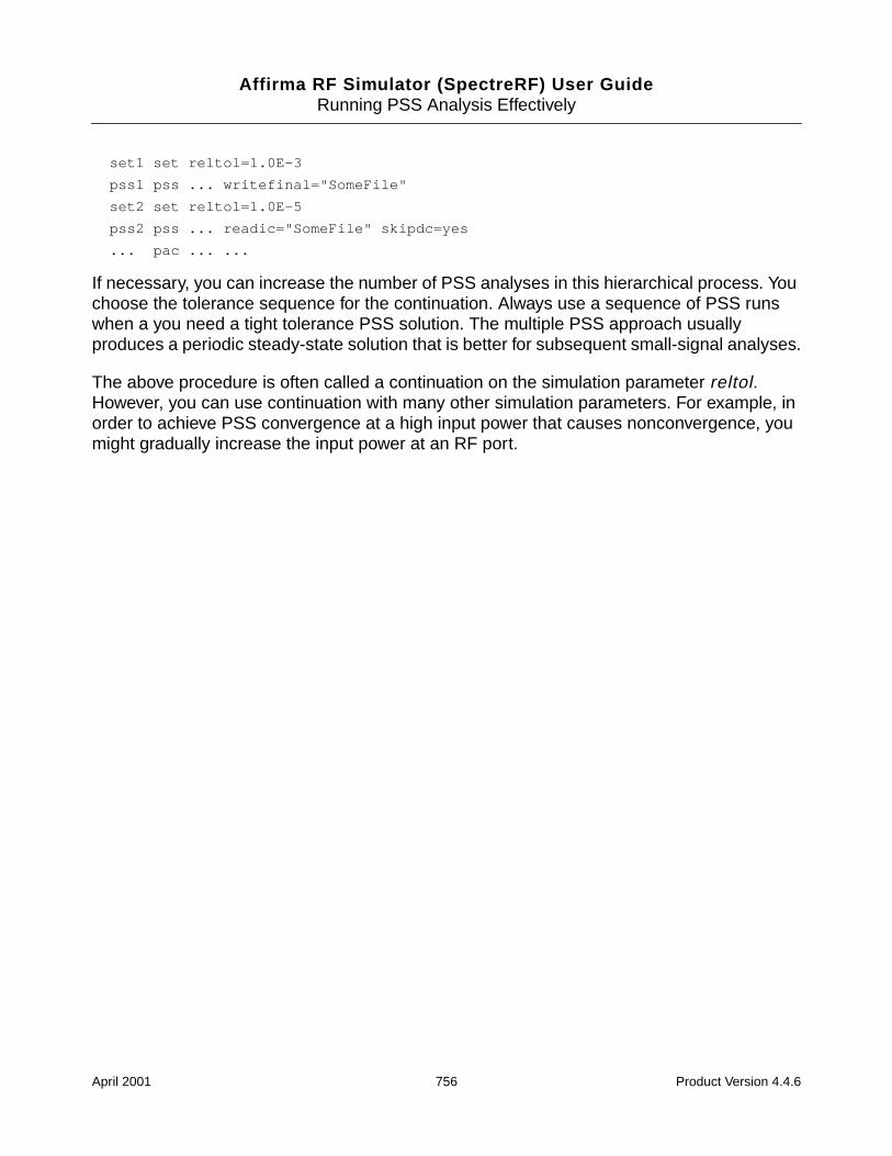
Affirma RF Simulator (SpectreRF) User GuideRunning PSS Analysis Effectively
set1 set reltol=1.0E-3
pss1 pss ... writefinal="SomeFile"
set2 set reltol=1.0E-5
pss2 pss ... readic="SomeFile" skipdc=yes
... pac ... ...
If necessary, you can increase the number of PSS analyses in this hierarchical process. Youchoose the tolerance sequence for the continuation. Always use a sequence of PSS runswhen a you need a tight tolerance PSS solution. The multiple PSS approach usuallyproduces a periodic steady-state solution that is better for subsequent small-signal analyses.
The above procedure is often called a continuation on the simulation parameter reltol.However, you can use continuation with many other simulation parameters. For example, inorder to achieve PSS convergence at a high input power that causes nonconvergence, youmight gradually increase the input power at an RF port.
April 2001 756 Product Version 4.4.6
Affirma RF Simulator (SpectreRF) User Guide
CUsing the psin Component
The procedures described in this appendix are deliberately broad and generic. Requirementsfor your specific design might dictate procedures slightly different from those described here.
This appendix describes how to use the psin component from the analogLib library inSpectreRF simulations within the Affirma™ analog circuit design environment.
Independent Resistive Source (psin)
The psin component, located in the analogLib library, is used in all RF circuits forSpectreRF and Spectre S-parameter simulations.
When you netlist psin in the Affirma analog circuit design environment using the SpectreSsimulator, you can see that psin is the port component in Spectre simulation. A port is aresistive source that is tied between positive and negative terminals. It is equivalent to avoltage source in series with a resistor, and the reference resistance of the port is the valueof the resistor.
psin Capabilities
While the psin is generally useful as a stimulus in high-frequency circuits, it also has thefollowing three unique capabilities:
Defines the ports of the circuit to the S-parameter analysis
Has an intrinsic noise source that lets the noise analysis directly compute the noisefigure of the circuit
Is the only source for which the amplitude can be specified in terms of power
Terminating the psin
Be aware that when you specify the voltage on a psin, Spectre assumes that the psin isproperly terminated in it’s reference resistance. The specified voltage value is not the
April 2001 757 Product Version 4.4.6
Affirma RF Simulator (SpectreRF) User GuideUsing the psin Component
voltage on the internal voltage source, which is actually set to twice the value specified on thepsin. So, if you use a psin source to drive an open circuit, the voltage (for DC, transient,AC, and PAC signals) is double its specified value. However, you can alternatively specify theamplitude of the sine wave in the transient and PACanalyses as the power in dBm deliveredby the psin when terminated with the reference resistance.
The psin component Edit Properties form is shown in Figure C-1 on page 759and inFigure C-2 on page 760.
April 2001 758 Product Version 4.4.6
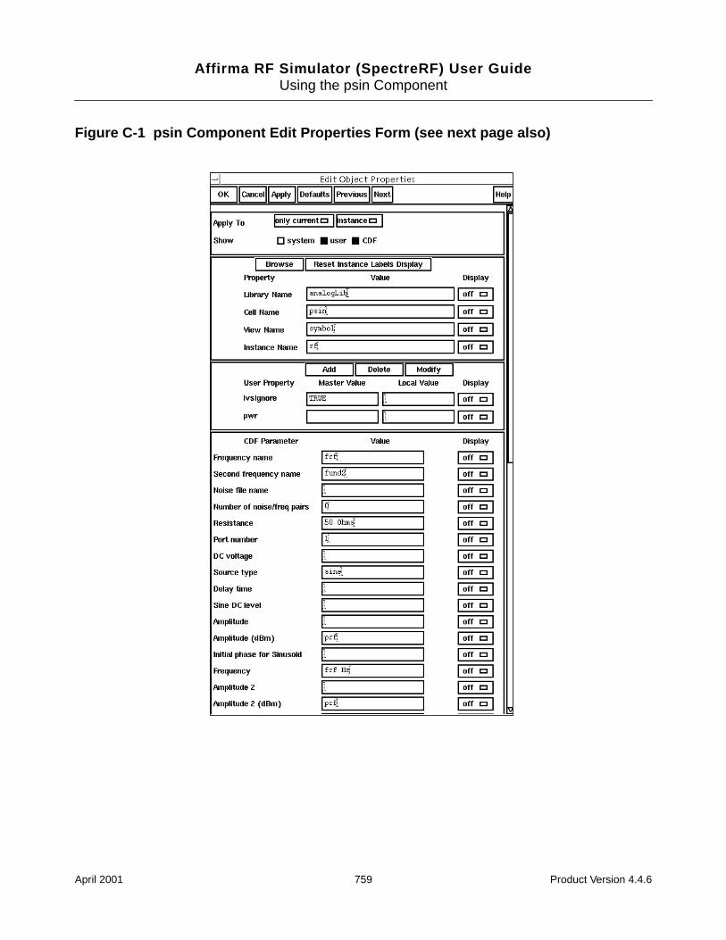
Affirma RF Simulator (SpectreRF) User GuideUsing the psin Component
Figure C-1 psin Component Edit Properties Form (see next page also)
April 2001 759 Product Version 4.4.6
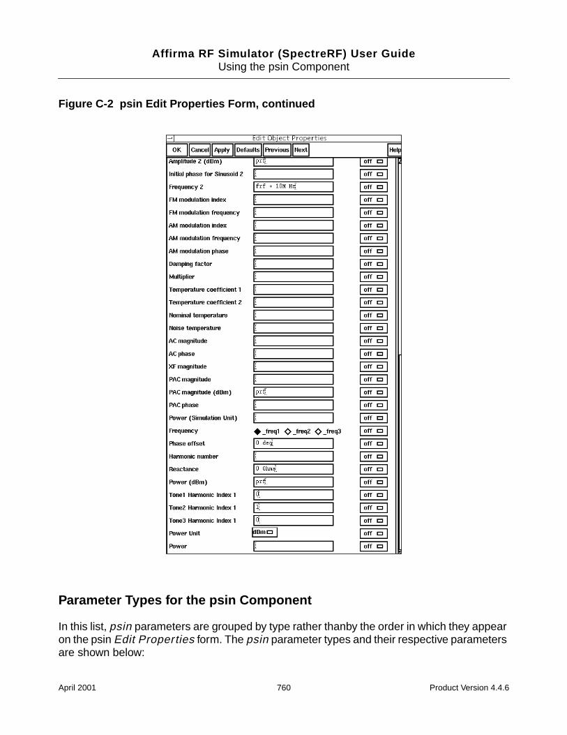
Affirma RF Simulator (SpectreRF) User GuideUsing the psin Component
Figure C-2 psin Edit Properties Form, continued
Parameter Types for the psin Component
In this list, psin parameters are grouped by type rather thanby the order in which they appearon the psin Edit Properties form. The psin parameter types and their respective parametersare shown below:
April 2001 760 Product Version 4.4.6
Affirma RF Simulator (SpectreRF) User GuideUsing the psin Component
Name Parameter s
Frequency name
Second frequency name
psin Instance P arameter
DC voltage
General W aveform P arameter s
Source type
Delay time
Sinusoidal W aveform Parameter s
Sine DC level
Amplitude
Amplitude (dBm)
Frequency
Initial phase for Sinusoid
Amplitude 2
Frequency 2
Phase for sinusoid 2
Amplitude Modulation P arameter s
AM modulation frequency
AM modulation phase
AM modulation index
FM Modulation P arameter s
FM modulation frequency
April 2001 761 Product Version 4.4.6
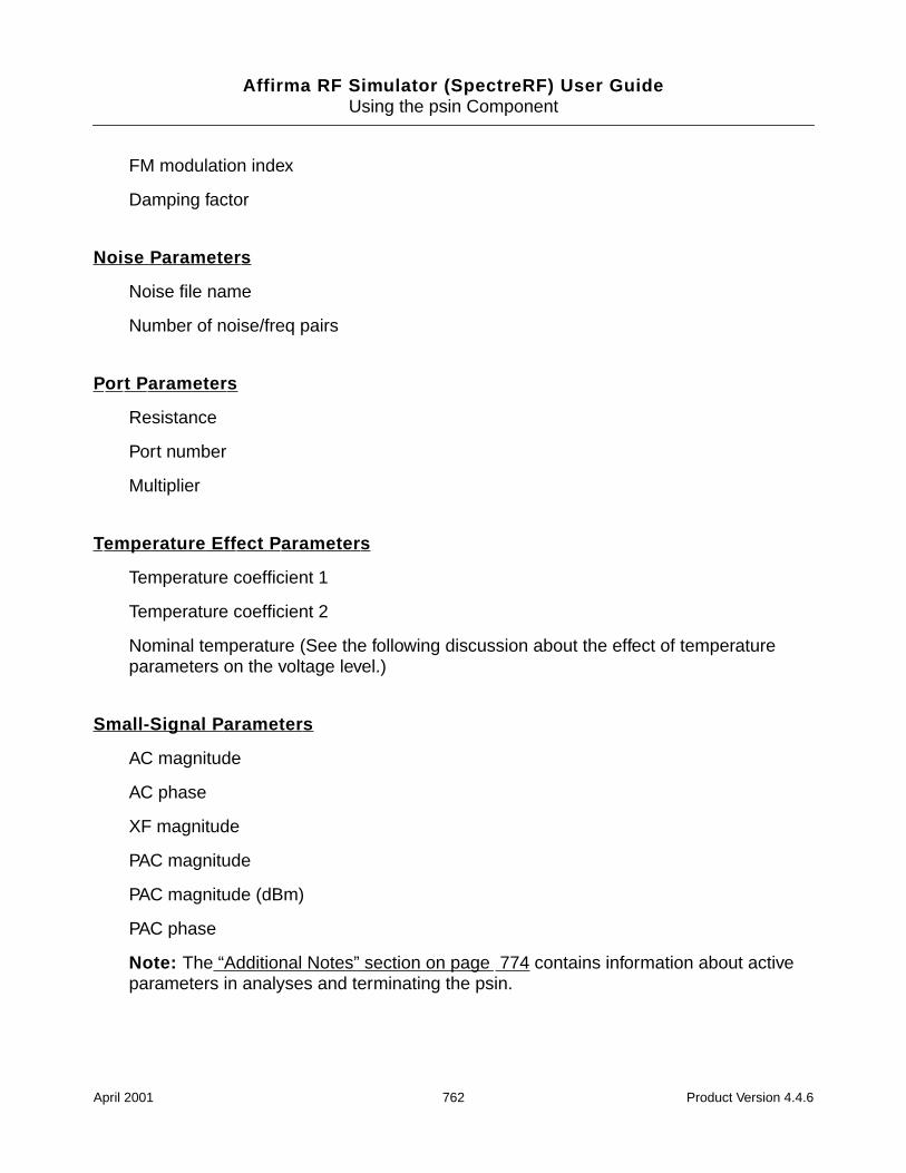
Affirma RF Simulator (SpectreRF) User GuideUsing the psin Component
FM modulation index
Damping factor
Noise P arameter s
Noise file name
Number of noise/freq pairs
Por t Parameter s
Resistance
Port number
Multiplier
Temperature Eff ect Parameter s
Temperature coefficient 1
Temperature coefficient 2
Nominal temperature (See the following discussion about the effect of temperatureparameters on the voltage level.)
Small-Signal P arameter s
AC magnitude
AC phase
XF magnitude
PAC magnitude
PAC magnitude (dBm)
PAC phase
Note: The “Additional Notes” section on page 774 contains information about activeparameters in analyses and terminating the psin.
April 2001 762 Product Version 4.4.6
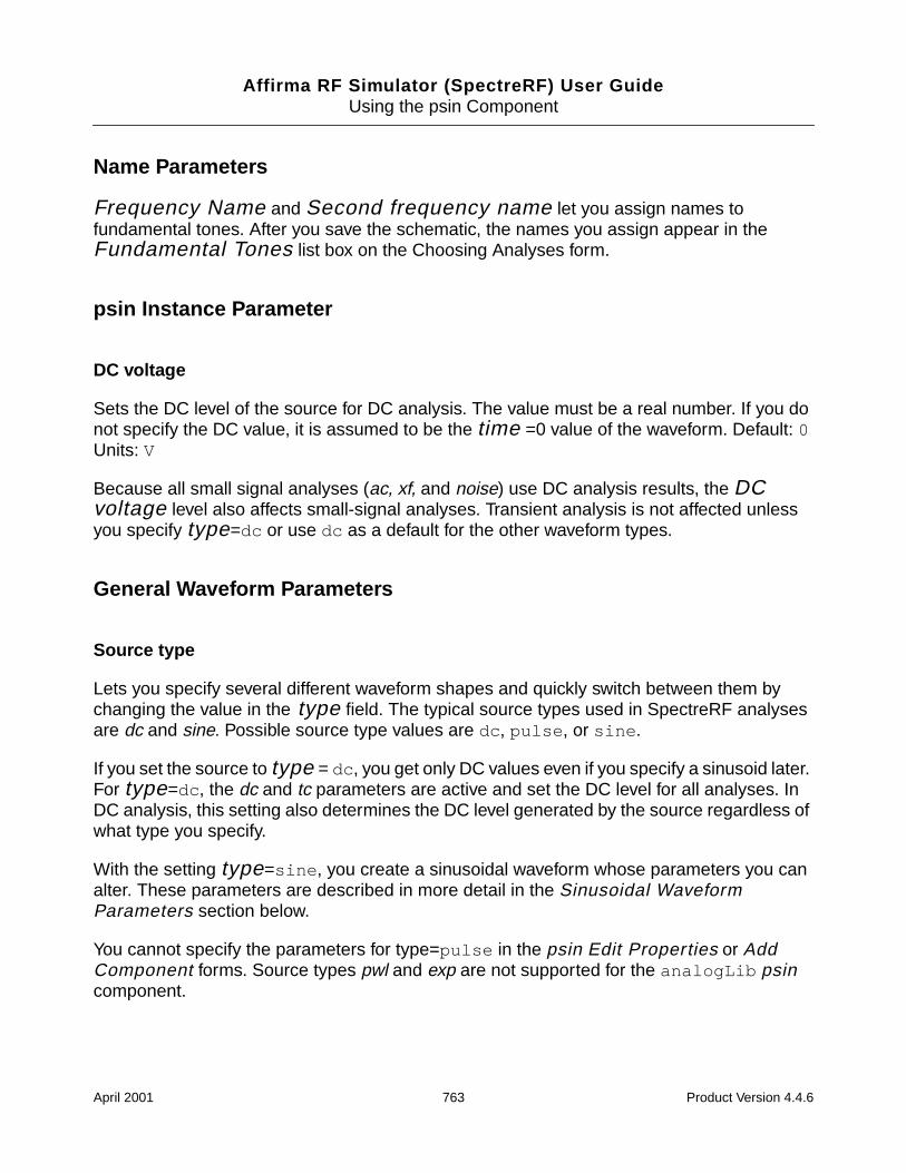
Affirma RF Simulator (SpectreRF) User GuideUsing the psin Component
Name Parameters
Frequency Name and Second frequency name let you assign names tofundamental tones. After you save the schematic, the names you assign appear in theFundamental Tones list box on the Choosing Analyses form.
psin Instance Parameter
DC voltage
Sets the DC level of the source for DC analysis. The value must be a real number. If you donot specify the DC value, it is assumed to be the time =0 value of the waveform. Default: 0Units: V
Because all small signal analyses (ac, xf, and noise) use DC analysis results, the DCvoltage level also affects small-signal analyses. Transient analysis is not affected unlessyou specify type=dc or use dc as a default for the other waveform types.
General Waveform Parameters
Source type
Lets you specify several different waveform shapes and quickly switch between them bychanging the value in the type field. The typical source types used in SpectreRF analysesare dc and sine. Possible source type values are dc , pulse , or sine .
If you set the source to type = dc , you get only DC values even if you specify a sinusoid later.For type=dc , the dc and tc parameters are active and set the DC level for all analyses. InDC analysis, this setting also determines the DC level generated by the source regardless ofwhat type you specify.
With the setting type=sine , you create a sinusoidal waveform whose parameters you canalter. These parameters are described in more detail in the Sinusoidal WaveformParameters section below.
You cannot specify the parameters for type=pulse in the psin Edit Properties or AddComponent forms. Source types pwl and exp are not supported for the analogLib psincomponent.
April 2001 763 Product Version 4.4.6
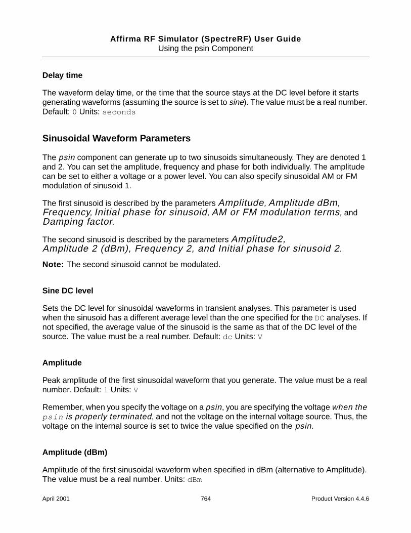
Affirma RF Simulator (SpectreRF) User GuideUsing the psin Component
Delay time
The waveform delay time, or the time that the source stays at the DC level before it startsgenerating waveforms (assuming the source is set to sine). The value must be a real number.Default: 0 Units: seconds
Sinusoidal Waveform Parameters
The psin component can generate up to two sinusoids simultaneously. They are denoted 1and 2. You can set the amplitude, frequency and phase for both individually. The amplitudecan be set to either a voltage or a power level. You can also specify sinusoidal AM or FMmodulation of sinusoid 1.
The first sinusoid is described by the parameters Amplitude, Amplitude dBm,Frequency, Initial phase for sinusoid, AM or FM modulation terms, andDamping factor.
The second sinusoid is described by the parameters Amplitude2,Amplitude 2 (dBm), Frequency 2, and Initial phase for sinusoid 2.
Note: The second sinusoid cannot be modulated.
Sine DC level
Sets the DC level for sinusoidal waveforms in transient analyses. This parameter is usedwhen the sinusoid has a different average level than the one specified for the DCanalyses. Ifnot specified, the average value of the sinusoid is the same as that of the DC level of thesource. The value must be a real number. Default: dc Units: V
Amplitude
Peak amplitude of the first sinusoidal waveform that you generate. The value must be a realnumber. Default: 1 Units: V
Remember, when you specify the voltage on a psin, you are specifying the voltage when thepsin is properly terminated, and not the voltage on the internal voltage source. Thus, thevoltage on the internal source is set to twice the value specified on the psin.
Amplitude (dBm)
Amplitude of the first sinusoidal waveform when specified in dBm (alternative to Amplitude).The value must be a real number. Units: dBm
April 2001 764 Product Version 4.4.6
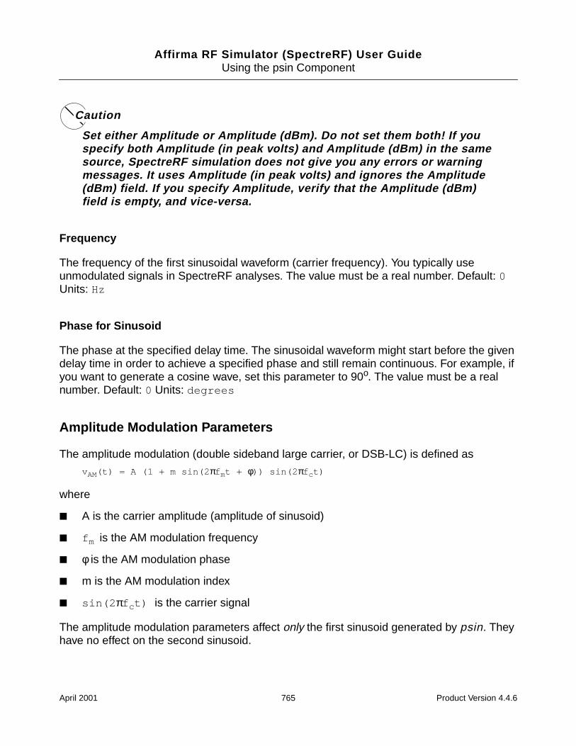
Affirma RF Simulator (SpectreRF) User GuideUsing the psin Component
Caution
Set either Amplitude or Amplitude (dBm). Do not set them both! If youspecify both Amplitude (in peak volts) and Amplitude (dBm) in the samesource, SpectreRF simulation does not give you any errors or warningmessages. It uses Amplitude (in peak volts) and ignores the Amplitude(dBm) field. If you specify Amplitude, verify that the Amplitude (dBm)field is empty, and vice-versa.
Frequency
The frequency of the first sinusoidal waveform (carrier frequency). You typically useunmodulated signals in SpectreRF analyses. The value must be a real number. Default: 0Units: Hz
Phase for Sinusoid
The phase at the specified delay time. The sinusoidal waveform might start before the givendelay time in order to achieve a specified phase and still remain continuous. For example, ifyou want to generate a cosine wave, set this parameter to 90o. The value must be a realnumber. Default: 0 Units: degrees
Amplitude Modulation Parameters
The amplitude modulation (double sideband large carrier, or DSB-LC) is defined as
vAM(t) = A (1 + m sin(2 πf mt + φ)) sin(2 πf ct)
where
A is the carrier amplitude (amplitude of sinusoid)
f m is the AM modulation frequency
φ is the AM modulation phase
m is the AM modulation index
sin(2 πf ct) is the carrier signal
The amplitude modulation parameters affect only the first sinusoid generated by psin. Theyhave no effect on the second sinusoid.
April 2001 765 Product Version 4.4.6
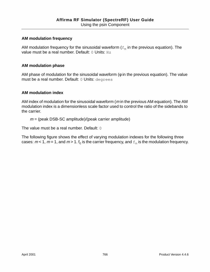
Affirma RF Simulator (SpectreRF) User GuideUsing the psin Component
AM modulation frequency
AM modulation frequency for the sinusoidal waveform (f m in the previous equation). Thevalue must be a real number. Default: 0 Units: Hz
AM modulation phase
AM phase of modulation for the sinusoidal waveform (φ in the previous equation). The valuemust be a real number. Default: 0 Units: degrees
AM modulation index
AM index of modulation for the sinusoidal waveform (m in the previous AM equation). The AMmodulation index is a dimensionless scale factor used to control the ratio of the sidebands tothe carrier.
m = (peak DSB-SC amplitude)/(peak carrier amplitude)
The value must be a real number. Default: 0
The following figure shows the effect of varying modulation indexes for the following threecases: m < 1, m = 1, and m > 1. fc is the carrier frequency, and f mis the modulation frequency.
April 2001 766 Product Version 4.4.6
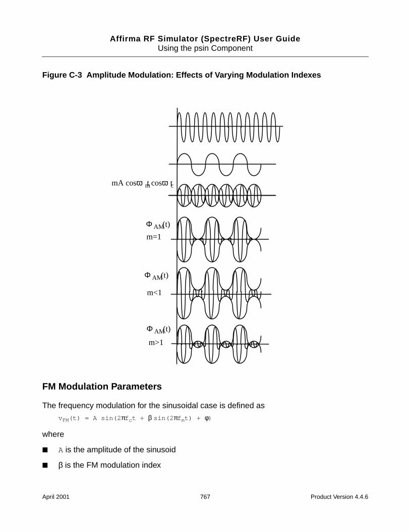
Affirma RF Simulator (SpectreRF) User GuideUsing the psin Component
Figure C-3 Amplitude Modulation: Effects of Varying Modulation Indexes
FM Modulation Parameters
The frequency modulation for the sinusoidal case is defined as
vFM(t) = A sin(2 πf ct + β sin(2 πf mt) + φ)
where
A is the amplitude of the sinusoid
β is the FM modulation index
Φ AM(t)
Φ AM(t)
Φ AM(t)
m>1
m=1
m<1
mA cosω mt cosω ct
April 2001 767 Product Version 4.4.6
Affirma RF Simulator (SpectreRF) User GuideUsing the psin Component
sin(2 πf mt) is the modulation signal
f c is the carrier frequency
φ is the phase of the sinusoid
The frequency modulation parameters affect only the first frequency generated by psin. Theyhave no effect on the second frequency.
FM modulation frequency
FM modulation frequency for the sinusoidal waveform (f m in the equation above). The valuemust be a real number. Default: 0 Units: Hz
FM modulation index
FM index of modulation for the sinusoidal waveform, the ratio of peak frequency deviationdivided by the center frequency (β in the above equations).
β=∆f/f m
The value must be a real number. Default: 0
Damping factor
Damping factor for the sinusoidal waveform. Damping factor specifies the time it takes to gofrom the envelope (full amplitude) at time=0 to 63 percent of the full amplitude. For example,consider the following damped sinusoid:
v(t) = A e −σt sin(2 πft + φ)
where σ= damping factor.
If σ = 0, the waveform is a pure sinusoid (steady state).
If σ < 0, the waveform exhibits decaying oscillations.
If σ > 0, the waveform exhibits growing oscillations.
It takes 5s to diminish to 1 percent of the peak amplitude. The value must be a real number.Default: 0. Units: 1/seconds
The following figure shows the effect of Damping factor on the first sinusoid for three valuesof σ.
April 2001 768 Product Version 4.4.6
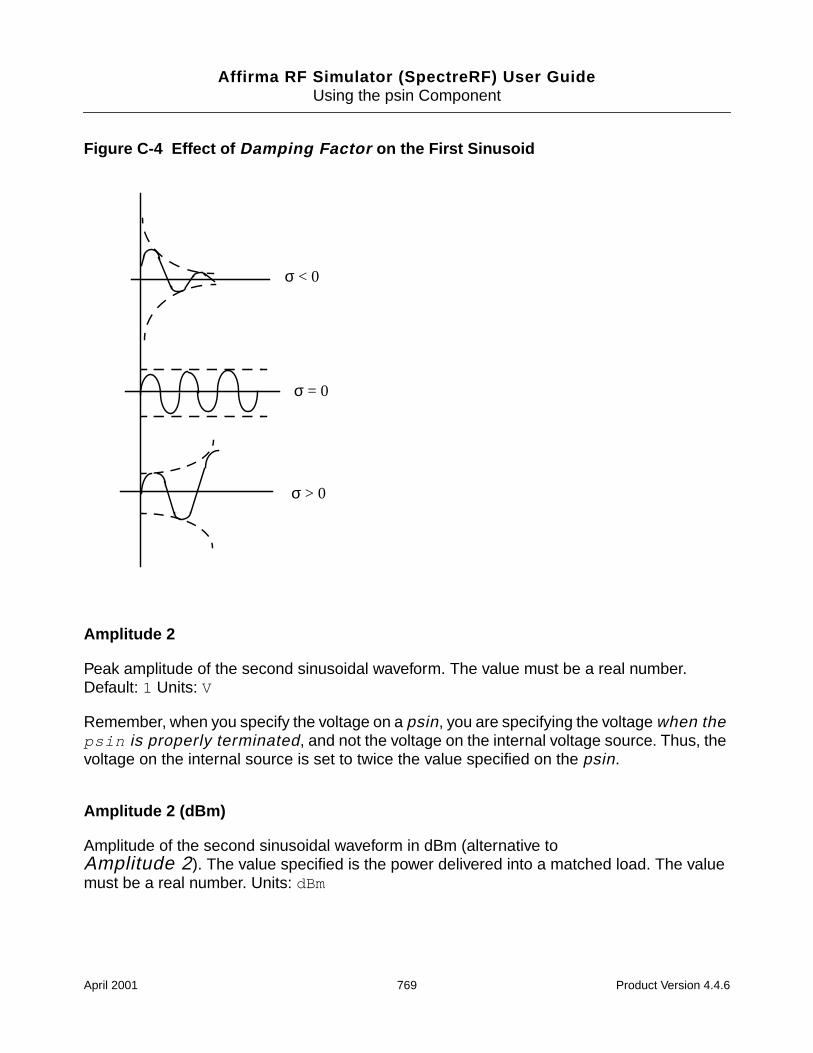
Affirma RF Simulator (SpectreRF) User GuideUsing the psin Component
Figure C-4 Effect of Damping Factor on the First Sinusoid
Amplitude 2
Peak amplitude of the second sinusoidal waveform. The value must be a real number.Default: 1 Units: V
Remember, when you specify the voltage on a psin, you are specifying the voltage when thepsin is properly terminated, and not the voltage on the internal voltage source. Thus, thevoltage on the internal source is set to twice the value specified on the psin.
Amplitude 2 (dBm)
Amplitude of the second sinusoidal waveform in dBm (alternative toAmplitude 2). The value specified is the power delivered into a matched load. The valuemust be a real number. Units: dBm
σ = 0
σ < 0
σ > 0
April 2001 769 Product Version 4.4.6
Affirma RF Simulator (SpectreRF) User GuideUsing the psin Component
Caution
Set either Amplitude2 or Amplitude2 (dBm). Do not set them both!
Frequency 2
Frequency of the second sinusoidal waveform. The value must be a real number. Default: 0Units: Hz
Phase for Sinusoid 2
The phase at the specified Delay time for the second sinusoid. The sinusoidal waveformmight start before the given Delay time in order to achieve specified phase while stillremaining continuous. The value must be a real number. Default: 0 Units: degrees
Noise Parameters
Noise parameters include Noise file name, Number of Noise Frequency Pairs,and Noise temperature.
Noise file name
Name of the file containing the excess spot noise data in the form of frequency-noise pairs.The value must be a string. Default: no value
Number of noise/freq. pairs
You must specify the number of noise-frequency pairs that exist in your noise file in the form.In your file, list the noise-frequency pairs as one pair per line with a space or tab between thefrequency and noise values. The values are given as a vector of real number pairs, wherenoise is given in V2/Hz, and frequency is given in Hz.
Specific to Affirma analog circuit design environment netlisting: If you have morenoise-frequency pairs than the number you specify in the Number of noise frequency pairsfield, the number of noise-frequency pairs used is the number you specify in the field. Anyadditional noise-frequency pairs in the noise file are ignored. If the number of noise-frequencypairs in the noise file is smaller than the number you specified in the number of noisefrequency pairs field, the analysis is stopped.
April 2001 770 Product Version 4.4.6
Affirma RF Simulator (SpectreRF) User GuideUsing the psin Component
Noise temperature
The Noise temperature of the psin. If not specified, the Noise temperature is assumed tobe the actual temperature of the psin. When you compute the noise figure of a circuit drivenat its input by a psin, set the noise temperature of the psin (Spectre parameter noisetemp)to 16.85C (290K). This setting matches the standard IEEE definition of noise figure. Inaddition, disable all other sources of noise in the psin, such as the Spectre parametersnoisefile and noisevec. If you want a noiseless psin, set the noise temperature toabsolute zero or below, and do not specify a noise file or noise vector. Default: Units: oC.
Port Parameters
Port parameters include Resistance, Port Number, and Multiplier.
Resistance
The reference resistance of the system. The value must be a real number, but not 0. Default:50 Units: Ω
Port number
The number of the port. The value must be a nonzero integer. Each psin in a schematic musthave a different port number. The Port number is not automatically indexed when you placeeach psin on your schematic.
Multiplier
The multiplicity factor. The value must be an integer number greater than zero. This numberlets you specify a number of psins in parallel. For example, if you set Resistance to 50 andMultiplier to 2, you specify two psin ports in parallel, each with an effective referenceresistance of 25 Ω. Default: 1
Temperature Effect Parameters
How Temperature Parameters Affect the Voltage Level (Background Information)
The value of the DC voltage can vary as a function of the temperature if you specify tc1 andtc2. The variation is given by
VDC( T) = dc * [1 + tc1 * ( T – tnom) + tc2 * ( T – tnom) 2]
April 2001 771 Product Version 4.4.6
Affirma RF Simulator (SpectreRF) User GuideUsing the psin Component
where T is the analysis temperature specified in the analysis options, tnom is the nominaltemperature specified in the Choosing Analyses form, and dc is the DC voltage.
If the analysis temperature equals the nominal temperature, the result is the voltageamplitude that you specified, VDC(T)= dc .
If the nominal and analysis temperatures differ, the voltage amplitude is given by
VDC(T) = dc * [1 + tc1 * (T – tnom) + tc2 * (T – tnom)2]
where T is the analysis temperature you specify in the analysis options and tnom is thenominal temperature. tc1 and tc2 are the linear and quadratic temperature coefficients.
For example, if the nominal temperature is 27oC and the analysis temperature is 25oC, thereis a 2o difference between the nominal and analysis temperature. The voltage amplitude is
VDC( T) = dc * [1 + tc1 * (–2) + tc2 * (–2) 2]
Temperature effect parameters include Temperature coefficient 1 (the lineartemperature coefficient), Temperature coefficient 2 (the quadratic temperaturecoefficient), and Nominal temperature.
Temperature coefficient 1
First order (linear) temperature coefficient of the DC voltage (tc1). The value must be areal number. Default: 0 Units: o C-1
Temperature coefficient 2
Second order (quadratic) temperature coefficient of the DC voltage (tc2) . The value mustbe a real number. Default: 0 Units: o C-2
Nominal temperature
The nominal temperature for DC voltage (tnom) . The value must be a real number. Default:Set by options specifications Units: C
Small-Signal Parameters
The small signal parameters are AC magnitude, AC phase, XF magnitude, PACmagnitude, PAC magnitude (dBm), and PAC phase.
April 2001 772 Product Version 4.4.6

Affirma RF Simulator (SpectreRF) User GuideUsing the psin Component
Remember, when you specify the voltage on a psin, you are specifying the voltage whenthe psin is properly terminated, and not the voltage on the internal voltage source. Thus,the voltage on the internal source is set to twice the value specified on the psin. The sameis true for the values for the transient, AC, and PAC signals. However, the amplitude ofthe sine wave in the PAC and transient analysis can alternatively be specified as thepower in dBm delivered by the psin when terminated with the reference resistance
AC magnitude
The peak small-signal voltage. The value must be a real number. Default: 0 Units: V
AC phase
The small-signal phase. The value must be a real number. Default: 0 Units: degrees
Typically, only one source in the circuit has AC Magnitude set to a value other than zero, andusually it has an AC magnitude=1 and AC phase=0. However, there are situations wheremore than one source has a nonzero AC magnitude. For example, applying a differentialsmall-signal input could be done with two sources with the AC magnitudes set to 0.5 andthe AC phases set to 0 and 180.
XF magnitude
The transfer function analysis magnitude. Use XF magnitude to compensate for gain orloss in the test fixture. The value must be a real number. Default: 1 Units: V/V
PAC magnitude
The peak periodic AC analysis magnitude. Setting this value to unity is a convenient way ofcomputing the transfer function from this source to the output. The value must be a realnumber. Default: 0 Units V
PAC magnitude (dBm)
The periodic AC analysis magnitude in dBm (alternative to PAC magnitude). The value mustbe a real number. Units: dBm
April 2001 773 Product Version 4.4.6
Affirma RF Simulator (SpectreRF) User GuideUsing the psin Component
Caution
Set either PAC magnitude or PAC magnitude (dBm), but do not set themboth!
PAC phase
The periodic AC analysis phase. The value must be a real number. Default: 0 Units: degrees
Typically, only one source in the circuit has a PAC magnitude set to a value other than zero,and usually it has a PAC magnitude=1 and PAC phase=0. However, there are situationswhere more than one source has a nonzero PAC magnitude. For example, applying adifferential small-signal input could be done with two sources with the PAC magnitudes setto 0.5 and the PAC phases set to 0 and 180."
You do not specify the PAC frequency in the psin Edit Object Properties form. Instead,you set the PAC frequency in the PAC Choosing Analysis form. For example, whenmaking an IP3 measurement, you set the PAC frequency to a variable value in the ChoosingAnalysis Form. Then, you enter the same variable in the PAC Amplitude (or PACAmplitude dBm) field of the psin Edit Object Properties form.
Additional Notes
Active Parameters in Analyses
In DC analyses, the only active parameters are dc, m, and the temperature coefficientparameters.
In AC analyses, the only active parameters are m, mag and phase.
In Transient analyses, all parameters are active except the small-signal parameters and thenoise parameters.
In PAC analyses , the only active parameters are m, PAC magnitude (amplitude or dBm), andPAC phase.
XF magnitude is active in XF and PXF analyses only.
April 2001 774 Product Version 4.4.6
Affirma RF Simulator (SpectreRF) User Guide
DThe RF Library
The RF Library, rfLib, is divided into four categories.
Models for top-down design,.top_dwnRF. It contains all of the elements of the originalrfLib. The models in top_dwnRFare the only models in rfLib designed specifically towork with SpectreRF. These models do not have hidden state.
Models for bottom-up design, bot_upBB. It currently contains only J-models.
Models used only for testing, test_bench. You would not actually build any of them.Currently test_bench contains a CDMA signal source, a GSM signal source, a P/4-DQPSK signal source, and an eye-diagram generator.
Models that are unclassified. This category contains files generated by the Testbenchmodels.
This appendix explains the models contained in each category.
Top-Down Design Elements
If you are an RF circuit designer who creates top-down designs, you must model functionalRF blocks at the behavioral level. These high-level models can be building-blocks for complexRF systems or executable specifications. When distributed in source code format, thesemodels also help you write libraries that reflect your own design needs.
The Verilog-A lets you use the new RF library models in the Spectre®RF circuit simulatorwithout an explicit equivalent circuit. This approach uses the high-level description languagecapability of SpectreRF to create high-level models that capture the essential information ofRF functional blocks. You can then insert these models into regular RF circuits for simulation.The essential parameters are translated into coefficients and equations that describe therelations between the voltages and currents at the connecting nodes.
You can characterize most RF circuits with three sets of parameters:
Linear Parameters
April 2001 775 Product Version 4.4.6
Affirma RF Simulator (SpectreRF) User GuideThe RF Library
Nonlinear Parameters
Noise Parameters.
The RF HDL library contains these seven models, discussed in the sections that follow.
Filter
Balun
Low Noise Amplifier
Mixer
Power Amplifier
Oscillator
Quadrature Signal Generator
Phase Shifter
Figure D-1 shows the symbols used for the components that are available in this RF library.
April 2001 776 Product Version 4.4.6
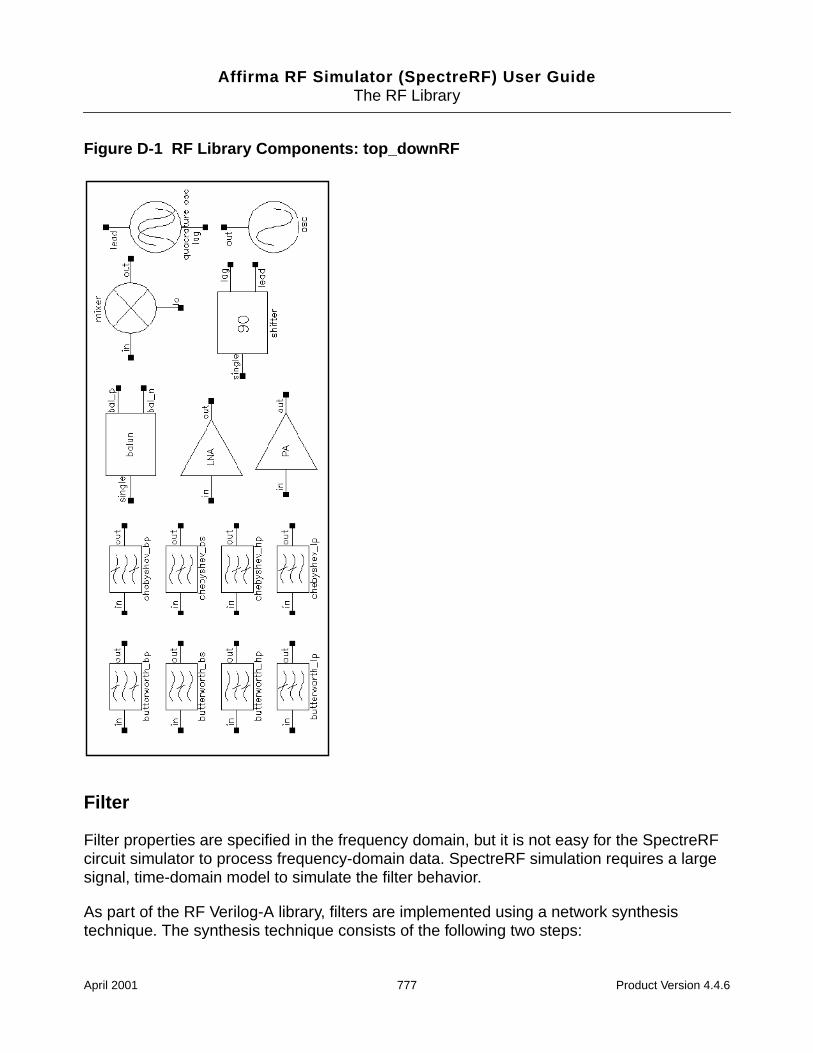
Affirma RF Simulator (SpectreRF) User GuideThe RF Library
Figure D-1 RF Library Components: top_downRF
Filter
Filter properties are specified in the frequency domain, but it is not easy for the SpectreRFcircuit simulator to process frequency-domain data. SpectreRF simulation requires a largesignal, time-domain model to simulate the filter behavior.
As part of the RF Verilog-A library, filters are implemented using a network synthesistechnique. The synthesis technique consists of the following two steps:
April 2001 777 Product Version 4.4.6
Affirma RF Simulator (SpectreRF) User GuideThe RF Library
1. Calculate the normalized low-pass filter prototype, which consists of serial inductors andparallel capacitors
2. Perform frequency transformation and scaling to synthesize the frequency responses ofthe filter type
The synthesized model contains many inductors and capacitors. They are implemented usingthe integral and differential functions of the Verilog-A language, and insertion loss is addedusing the S-parameter network technique. This network essentially dampens the signal flowby the specified insertion loss value.
Low-pass, high-pass, bandpass, and bandstop filters are implemented, and each of thesecan be a Butterworth or Chebyshev type filter (for a total of eight combinations). In the currentimplementation of the Verilog-A language, the order and internal states of the filter cannot bedynamically allocated. You must use the ’define derivative in the source code of theVerilog-A file to specify the order. Use S-parameters to test the filters because S-parameterscapture the input/output impedance matching.
For example, the Butterworth bandpass filter has the following module declaration:
module butterworth_bp(t1, t2);
inout t1, t2;
electrical in, out;
parameter real r1 = 50 from (0:inf);
parameter real r2 = 50 from (0:inf);
parameter real f0 = 1e9 from (0:inf);
parameter real bw = 0.10 from (0:0.5);
parameter real fc = 1e9 from (0:inf);
parameter real loss = 0 from [0:inf);
where t1 and t2 are the input and output nodes, respectively.
The parameters are
r1 Input impedance [Ω]
r2 Output impedance [Ω]
fc Corner frequency (3dB point) for low-pass and high-pass filter [Hz]
f0 Center frequency for bandpass or bandstop filter [Hz]
bw Relative frequency for bandpass or bandstop filter [Hz]
loss Insertion loss [dB]
April 2001 778 Product Version 4.4.6
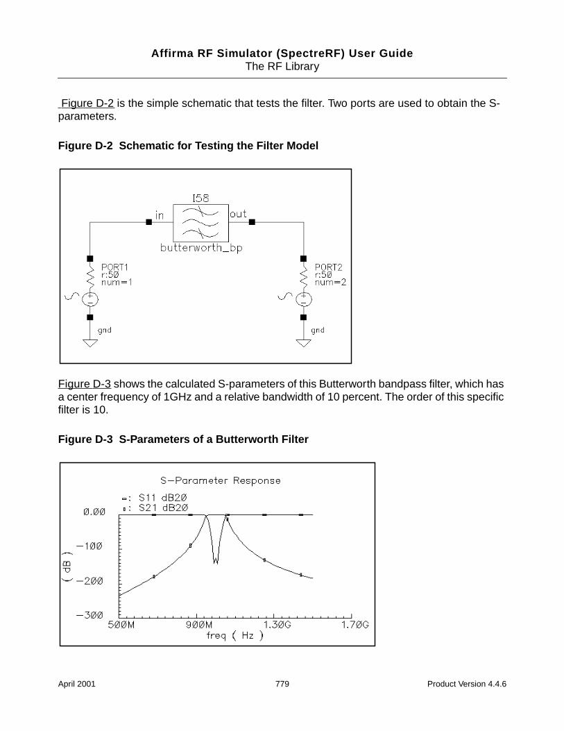
Affirma RF Simulator (SpectreRF) User GuideThe RF Library
Figure D-2 is the simple schematic that tests the filter. Two ports are used to obtain the S-parameters.
Figure D-2 Schematic for Testing the Filter Model
Figure D-3 shows the calculated S-parameters of this Butterworth bandpass filter, which hasa center frequency of 1GHz and a relative bandwidth of 10 percent. The order of this specificfilter is 10.
Figure D-3 S-Parameters of a Butterworth Filter
April 2001 779 Product Version 4.4.6
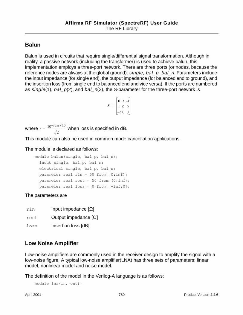
Affirma RF Simulator (SpectreRF) User GuideThe RF Library
Balun
Balun is used in circuits that require single/differential signal transformation. Although inreality, a passive network (including the transformer) is used to achieve balun, thisimplementation employs a three-port network. There are three ports (or nodes, because thereference nodes are always at the global ground): single, bal_p, bal_n. Parameters includethe input impedance (for single end), the output impedance (for balanced end to ground), andthe insertion loss (from single end to balanced end and vice versa). If the ports are numberedas single(1), bal_p(2), and bal_n(3), the S-parameter for the three-port network is
where when loss is specified in dB.
This module can also be used in common mode cancellation applications.
The module is declared as follows:
module balun(single, bal_p, bal_n);
inout single, bal_p, bal_n;
electrical single, bal_p, bal_n;
parameter real rin = 50 from (0:inf);
parameter real rout = 50 from (0:inf);
parameter real loss = 0 from (-inf:0];
The parameters are
Low Noise Amplifier
Low-noise amplifiers are commonly used in the receiver design to amplify the signal with alow-noise figure. A typical low-noise amplifier(LNA) has three sets of parameters: linearmodel, nonlinear model and noise model.
The definition of the model in the Verilog-A language is as follows:
module lna(in, out);
rin Input impedance [Ω]
rout Output impedance [Ω]
loss Insertion loss [dB]
S0 t t–
t 0 0
t– 0 0
=
t10 loss– 10⁄
2---------------------------=
April 2001 780 Product Version 4.4.6
Affirma RF Simulator (SpectreRF) User GuideThe RF Library
inout in, out;
electrical in, out;
parameter real nf = 2 from [0:inf);
parameter real ip3 = -10;
parameter real gain = 15 from [0:inf);
parameter real isolation = 200 from (0:inf);
parameter real rin = 50 from (0:inf);
parameter real cin = 0 from [0:100];
parameter real rout = 50 from (0:inf);
parameter real cout = 0 from [0:100];
parameter real gammain = -150 from (-inf:0];
parameter real mismatch = 1 from [-1:1] exclude (-1:1);
parameter real gammaout=-150 from (-inf:0];
The parameters are
Internally, a set of linear equations is constructed to satisfy the S-parameters. Furthermore,nonlinearity, expressed by a third-order polynomial function, is added to the gain (or S21) todescribe the IP3. Excess white noise is added at the input port to describe the noise figure.
IP3 is the measure of the corruption of signals because of the third-order intermodulation oftwo nearby tones as shown in Figure D-4. You measure this parameter using a two-tone test.
nf Noise figure [dB]
ip3 Input referenced IP3 [dBm]
gain S21 (power gain) [dB]
isolation S12 [dB]
rin Reference impedance of the input port[Ω]
rout Reference impedance of the output port[Ω]
gammain Input return loss [dB]
mismatch Mismatch sign of input. 1: input impedance > referenceimpedance -1: otherwise
gammaout Output return loss [dB]
cin Parasitic input capacitance [pF]
cout Parasitic parallel output capacitance [pF]
April 2001 781 Product Version 4.4.6
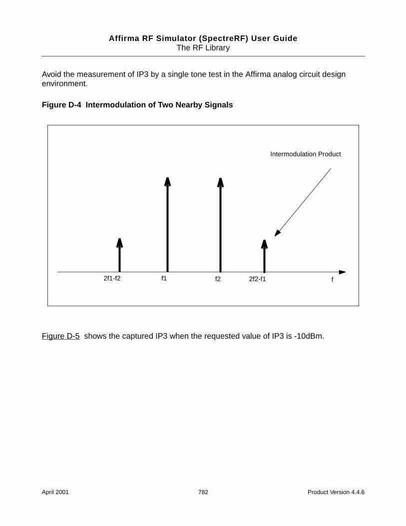
Affirma RF Simulator (SpectreRF) User GuideThe RF Library
Avoid the measurement of IP3 by a single tone test in the Affirma analog circuit designenvironment.
Figure D-4 Intermodulation of Two Nearby Signals
Figure D-5 shows the captured IP3 when the requested value of IP3 is -10dBm.
2f1-f2 f1 f2 2f2-f1
Intermodulation Product
f
April 2001 782 Product Version 4.4.6
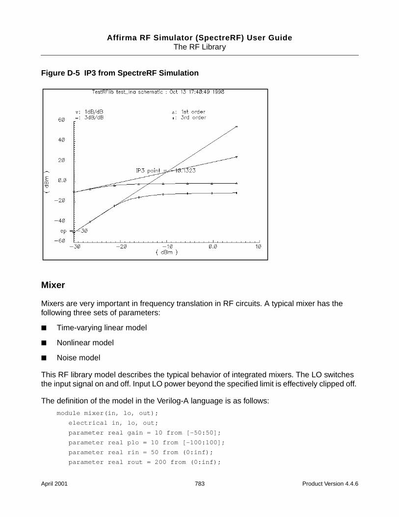
Affirma RF Simulator (SpectreRF) User GuideThe RF Library
Figure D-5 IP3 from SpectreRF Simulation
Mixer
Mixers are very important in frequency translation in RF circuits. A typical mixer has thefollowing three sets of parameters:
Time-varying linear model
Nonlinear model
Noise model
This RF library model describes the typical behavior of integrated mixers. The LO switchesthe input signal on and off. Input LO power beyond the specified limit is effectively clipped off.
The definition of the model in the Verilog-A language is as follows:
module mixer(in, lo, out);
electrical in, lo, out;
parameter real gain = 10 from [-50:50];
parameter real plo = 10 from [-100:100];
parameter real rin = 50 from (0:inf);
parameter real rout = 200 from (0:inf);
April 2001 783 Product Version 4.4.6
Affirma RF Simulator (SpectreRF) User GuideThe RF Library
parameter real rlo = 50 from (0:inf);
parameter real ip2 = 5;
parameter real ip3 = 5;
parameter real nf = 2 from [0:inf);
parameter real isolation_LO2IN = 20 from (0:inf);
parameter real isolation_LO2OUT = 20 from (0:inf);
parameter real isolation_IN2OUT = 20 from (0:inf);
The parameters are
Figure D-6 on page 785is the simple schematic that tests the filter.
gain Gain from IN to OUT [dB]
plo Power of the LO input [dBm]
rin Input impedance for IN [Ω]
rout Output impedance for OUT [Ω]
rlo Input impedance for LO [Ω]
ip2 Input referenced IP2 [dBm]
ip3 Input referenced IP3 [dBm]
nf Noise figure (SSB) [dB]
isolation_LO2IN Isolation from LO to IN [dB]
isolation_LO2OUT Isolation from LO to OUT [dB]
isolation_IN2OUT Isolation from IN to OUT [dB]
April 2001 784 Product Version 4.4.6
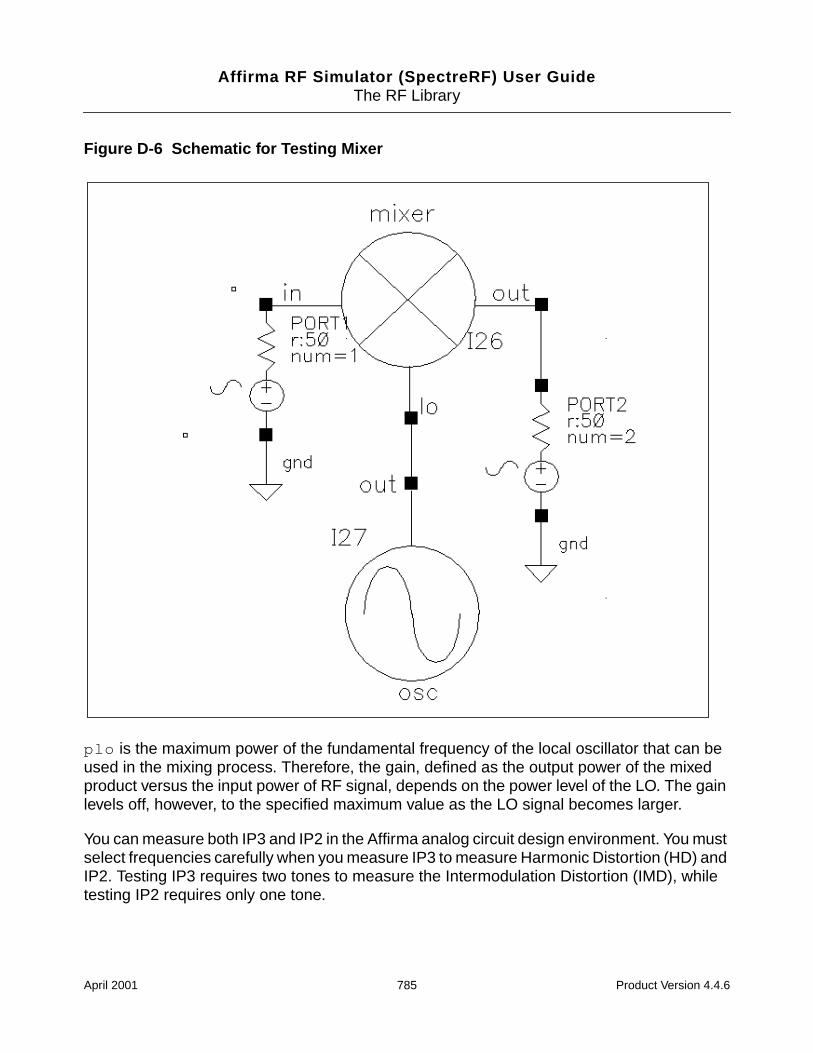
Affirma RF Simulator (SpectreRF) User GuideThe RF Library
Figure D-6 Schematic for Testing Mixer
plo is the maximum power of the fundamental frequency of the local oscillator that can beused in the mixing process. Therefore, the gain, defined as the output power of the mixedproduct versus the input power of RF signal, depends on the power level of the LO. The gainlevels off, however, to the specified maximum value as the LO signal becomes larger.
You can measure both IP3 and IP2 in the Affirma analog circuit design environment. You mustselect frequencies carefully when you measure IP3 to measure Harmonic Distortion (HD) andIP2. Testing IP3 requires two tones to measure the Intermodulation Distortion (IMD), whiletesting IP2 requires only one tone.
April 2001 785 Product Version 4.4.6
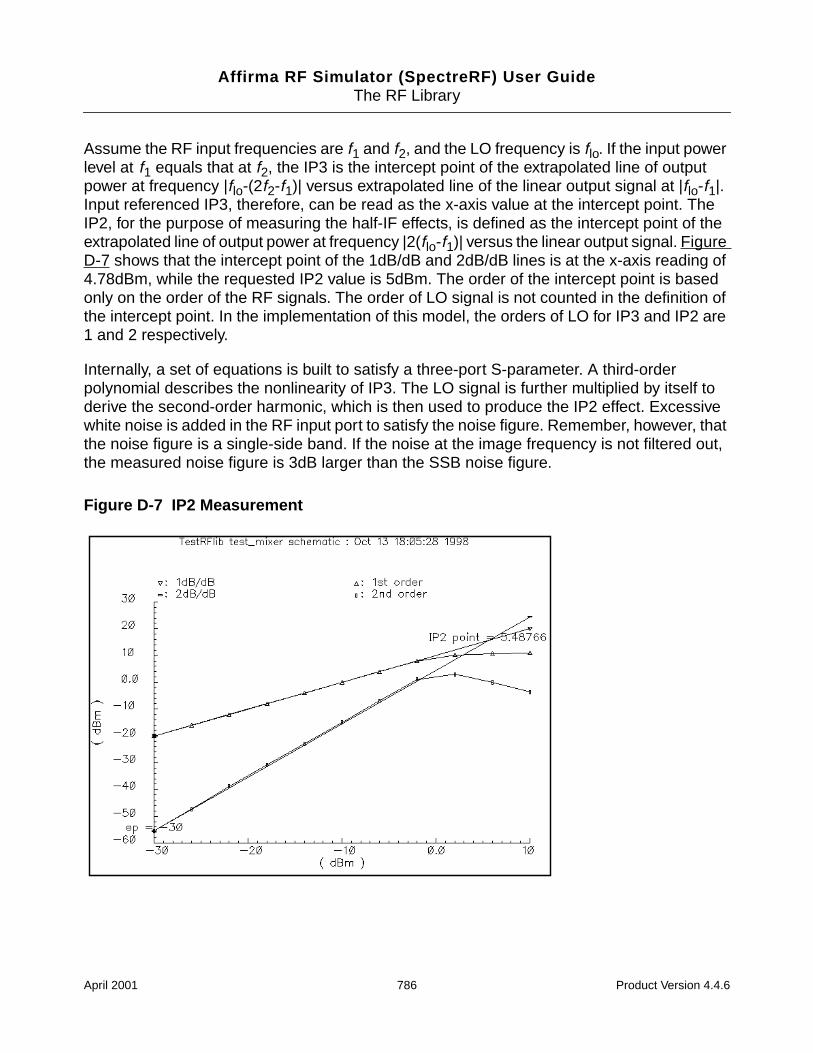
Affirma RF Simulator (SpectreRF) User GuideThe RF Library
Assume the RF input frequencies are f1 and f2, and the LO frequency is flo. If the input powerlevel at f1 equals that at f2, the IP3 is the intercept point of the extrapolated line of outputpower at frequency |flo-(2f2-f1)| versus extrapolated line of the linear output signal at |flo-f1|.Input referenced IP3, therefore, can be read as the x-axis value at the intercept point. TheIP2, for the purpose of measuring the half-IF effects, is defined as the intercept point of theextrapolated line of output power at frequency |2(flo-f1)| versus the linear output signal. FigureD-7 shows that the intercept point of the 1dB/dB and 2dB/dB lines is at the x-axis reading of4.78dBm, while the requested IP2 value is 5dBm. The order of the intercept point is basedonly on the order of the RF signals. The order of LO signal is not counted in the definition ofthe intercept point. In the implementation of this model, the orders of LO for IP3 and IP2 are1 and 2 respectively.
Internally, a set of equations is built to satisfy a three-port S-parameter. A third-orderpolynomial describes the nonlinearity of IP3. The LO signal is further multiplied by itself toderive the second-order harmonic, which is then used to produce the IP2 effect. Excessivewhite noise is added in the RF input port to satisfy the noise figure. Remember, however, thatthe noise figure is a single-side band. If the noise at the image frequency is not filtered out,the measured noise figure is 3dB larger than the SSB noise figure.
Figure D-7 IP2 Measurement
April 2001 786 Product Version 4.4.6
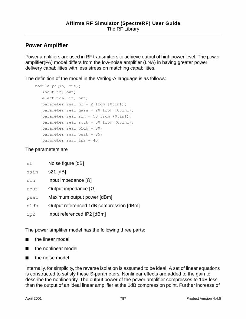
Affirma RF Simulator (SpectreRF) User GuideThe RF Library
Power Amplifier
Power amplifiers are used in RF transmitters to achieve output of high power level. The poweramplifier(PA) model differs from the low-noise amplifier (LNA) in having greater powerdelivery capabilities with less stress on matching capabilities.
The definition of the model in the Verilog-A language is as follows:
module pa(in, out);
inout in, out;
electrical in, out;
parameter real nf = 2 from [0:inf);
parameter real gain = 20 from [0:inf);
parameter real rin = 50 from (0:inf);
parameter real rout = 50 from (0:inf);
parameter real p1db = 30;
parameter real psat = 35;
parameter real ip2 = 40;
The parameters are
The power amplifier model has the following three parts:
the linear model
the nonlinear model
the noise model
Internally, for simplicity, the reverse isolation is assumed to be ideal. A set of linear equationsis constructed to satisfy these S-parameters. Nonlinear effects are added to the gain todescribe the nonlinearity. The output power of the power amplifier compresses to 1dB lessthan the output of an ideal linear amplifier at the 1dB compression point. Further increase of
nf Noise figure [dB]
gain s21 [dB]
rin Input impedance [Ω]
rout Output impedance [Ω]
psat Maximum output power [dBm]
p1db Output referenced 1dB compression [dBm]
ip2 Input referenced IP2 [dBm]
April 2001 787 Product Version 4.4.6
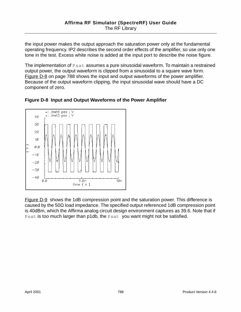
Affirma RF Simulator (SpectreRF) User GuideThe RF Library
the input power makes the output approach the saturation power only at the fundamentaloperating frequency. IP2 describes the second order effects of the amplifier, so use only onetone in the test. Excess white noise is added at the input port to describe the noise figure.
The implementation of Psat assumes a pure sinusoidal waveform. To maintain a restrainedoutput power, the output waveform is clipped from a sinusoidal to a square wave form.Figure D-8 on page 788 shows the input and output waveforms of the power amplifier.Because of the output waveform clipping, the input sinusoidal wave should have a DCcomponent of zero.
Figure D-8 Input and Output Waveforms of the Power Amplifier
Figure D-9 shows the 1dB compression point and the saturation power. This difference iscaused by the 50Ω load impedance. The specified output referenced 1dB compression pointis 40dBm, which the Affirma analog circuit design environment captures as 39.6. Note that ifPsat is too much larger than p1db, the Psat you want might not be satisfied.
April 2001 788 Product Version 4.4.6
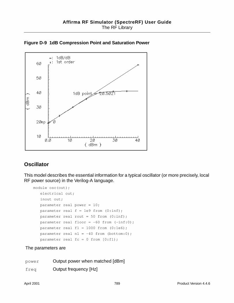
Affirma RF Simulator (SpectreRF) User GuideThe RF Library
Figure D-9 1dB Compression Point and Saturation Power
Oscillator
This model describes the essential information for a typical oscillator (or more precisely, localRF power source) in the Verilog-A language.
module osc(out);
electrical out;
inout out;
parameter real power = 10;
parameter real f = 1e9 from (0:inf);
parameter real rout = 50 from (0:inf);
parameter real floor = -60 from (-inf:0);
parameter real f1 = 1000 from (0:1e6);
parameter real n1 = -40 from (bottom:0);
parameter real fc = 0 from [0:f1);
The parameters are
power Output power when matched [dBm]
freq Output frequency [Hz]
April 2001 789 Product Version 4.4.6
Affirma RF Simulator (SpectreRF) User GuideThe RF Library
This model is not an autonomous model. Rather, it simply generates a sinusoidal wave withthe specified impedance, power level, and phase noise characteristics. When the load ismatched to the internal impedance, the load dissipates the specified output power. You canspecify the noise floor of the output signal. Furthermore, by adding one point (frequency,phase noise), you can specify 1/f2 frequency noise (corresponding to the phase noiseinduced by white noise). If fc, the corner frequency of white phase and flicker phase noise, isbigger than 0, 1/f3 frequency noise (flicker noise induced phase noise) is further specified.Otherwise, 1/f3 noise is not included.
The phase noises symmetric around the carrier are correlated. The noise floor, however, isnot correlated.
Figure D-10 on page 791 shows the phase noise of the oscillator model. The specifiedparameters are: noise floor = -60 dBc/Hz, f1=1 K, n1=-40 dBc/Hz, fc =100.
rout Output impedance [W]
floor Noise floor [dBc/Hz]
f1 Frequency point for n1 [Hz]
n1 Phase noise at f1 [dBc/Hz]
fc Corner frequency of white phase and flicker phase [Hz]
April 2001 790 Product Version 4.4.6
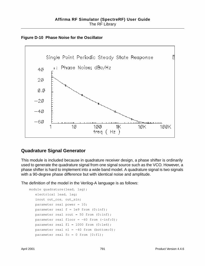
Affirma RF Simulator (SpectreRF) User GuideThe RF Library
Figure D-10 Phase Noise for the Oscillator
Quadrature Signal Generator
This module is included because in quadrature receiver design, a phase shifter is ordinarilyused to generate the quadrature signal from one signal source such as the VCO. However, aphase shifter is hard to implement into a wide band model. A quadrature signal is two signalswith a 90-degree phase difference but with identical noise and amplitude.
The definition of the model in the Verilog-A language is as follows:
module quadrature(lead, lag);
electrical lead, lag;
inout out_cos, out_sin;
parameter real power = 10;
parameter real f = 1e9 from (0:inf);
parameter real rout = 50 from (0:inf);
parameter real floor = -60 from (-inf:0);
parameter real f1 = 1000 from (0:1e6);
parameter real n1 = -40 from (bottom:0);
parameter real fc = 0 from [0:f1);
April 2001 791 Product Version 4.4.6
Affirma RF Simulator (SpectreRF) User GuideThe RF Library
The difference between this model and the oscillator model is that the oscillator has only oneoutput node, but the quadrature signal generator has two output nodes, lead and lag .When the power levels, output impedances, and noise sources are identical, the two outputshave a 90-degree phase difference.
Phase Shifter
In digital RF system designs, quadrature signal processing involves the phase splitting ofhigh-frequency signals. The most common use of such components is to generate twosignals that have a 90-degree phase difference based on one signal source (such as the RFsignal or oscillator output). Another common use is to combine two signals after adding a 90-degree phase difference, as in image-rejection receiver designs.
The definition of the model in the Verilog-A language is as follows:
module shifter(single, lag, lead);inout single, lag, lead;electrical single, lag, lead;parameter real freq = 1e9 from (0:inf);parameter real r = 50 from (0:inf);
The parameters are
Internally, the phase shifter is implemented using the RC-CR circuit as shown in Figure D-11on page 793. While the phase difference is also 90-degrees when the lead and lag have thesame output impedance, only at the operating frequency do the magnitudes remain thesame. This circuit network also generates white noise.
freq Frequency of operation [Hz]
r Resistance [Ω] (see Figure D-11)
April 2001 792 Product Version 4.4.6
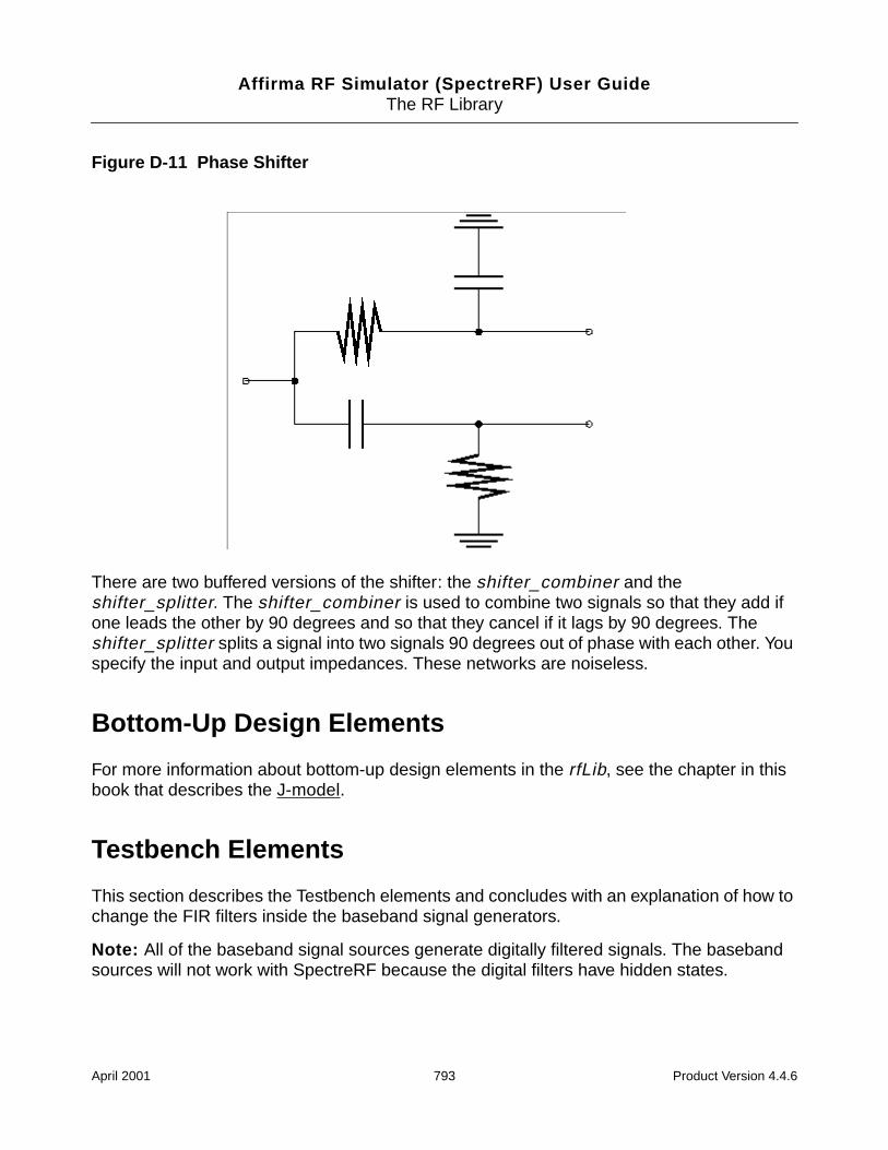
Affirma RF Simulator (SpectreRF) User GuideThe RF Library
Figure D-11 Phase Shifter
There are two buffered versions of the shifter: the shifter_combiner and theshifter_splitter. The shifter_combiner is used to combine two signals so that they add ifone leads the other by 90 degrees and so that they cancel if it lags by 90 degrees. Theshifter_splitter splits a signal into two signals 90 degrees out of phase with each other. Youspecify the input and output impedances. These networks are noiseless.
Bottom-Up Design Elements
For more information about bottom-up design elements in the rfLib, see the chapter in thisbook that describes the J-model.
Testbench Elements
This section describes the Testbench elements and concludes with an explanation of how tochange the FIR filters inside the baseband signal generators.
Note: All of the baseband signal sources generate digitally filtered signals. The basebandsources will not work with SpectreRF because the digital filters have hidden states.
April 2001 793 Product Version 4.4.6
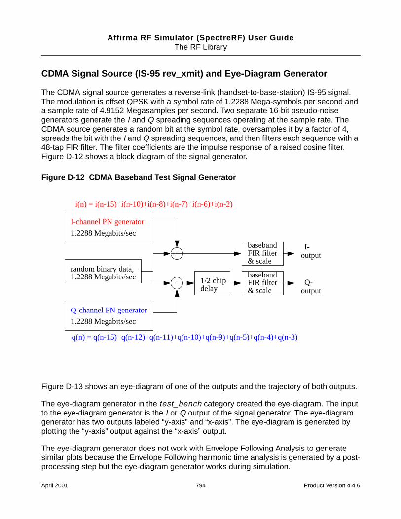
Affirma RF Simulator (SpectreRF) User GuideThe RF Library
CDMA Signal Source (IS-95 rev_xmit) and Eye-Diagram Generator
The CDMA signal source generates a reverse-link (handset-to-base-station) IS-95 signal.The modulation is offset QPSK with a symbol rate of 1.2288 Mega-symbols per second anda sample rate of 4.9152 Megasamples per second. Two separate 16-bit pseudo-noisegenerators generate the I and Q spreading sequences operating at the sample rate. TheCDMA source generates a random bit at the symbol rate, oversamples it by a factor of 4,spreads the bit with the I and Q spreading sequences, and then filters each sequence with a48-tap FIR filter. The filter coefficients are the impulse response of a raised cosine filter.Figure D-12 shows a block diagram of the signal generator.
Figure D-12 CDMA Baseband Test Signal Generator
Figure D-13 shows an eye-diagram of one of the outputs and the trajectory of both outputs.
The eye-diagram generator in the test_bench category created the eye-diagram. The inputto the eye-diagram generator is the I or Q output of the signal generator. The eye-diagramgenerator has two outputs labeled “y-axis” and “x-axis”. The eye-diagram is generated byplotting the “y-axis” output against the “x-axis” output.
The eye-diagram generator does not work with Envelope Following Analysis to generatesimilar plots because the Envelope Following harmonic time analysis is generated by a post-processing step but the eye-diagram generator works during simulation.
random binary data,1.2288 Megabits/sec
I-channel PN generator
1/2 chipdelay
basebandFIR filter
1.2288 Megabits/sec
Q-channel PN generator
1.2288 Megabits/sec
I-output
Q-output
& scale
basebandFIR filter& scale
i(n) = i(n-15)+i(n-10)+i(n-8)+i(n-7)+i(n-6)+i(n-2)
q(n) = q(n-15)+q(n-12)+q(n-11)+q(n-10)+q(n-9)+q(n-5)+q(n-4)+q(n-3)
April 2001 794 Product Version 4.4.6
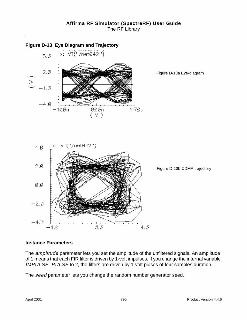
Affirma RF Simulator (SpectreRF) User GuideThe RF Library
Figure D-13 Eye Diagram and Trajectory
Instance Parameters
The amplitude parameter lets you set the amplitude of the unfiltered signals. An amplitudeof 1 means that each FIR filter is driven by 1-volt impulses. If you change the internal variableIMPULSE_PULSE to 2, the filters are driven by 1-volt pulses of four samples duration.
The seed parameter lets you change the random number generator seed.
Figure D-13a Eye-diagram
Figure D-13b CDMA trajectory
April 2001 795 Product Version 4.4.6
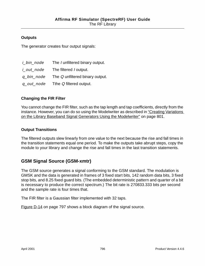
Affirma RF Simulator (SpectreRF) User GuideThe RF Library
Outputs
The generator creates four output signals:
Changing the FIR Filter
You cannot change the FIR filter, such as the tap length and tap coefficients, directly from theinstance. However, you can do so using the Modelwriter as described in “Creating Variationson the Library Baseband Signal Generators Using the Modelwriter” on page 801.
Output Transitions
The filtered outputs slew linearly from one value to the next because the rise and fall times inthe transition statements equal one period. To make the outputs take abrupt steps, copy themodule to your library and change the rise and fall times in the last transition statements.
GSM Signal Source (GSM-xmtr)
The GSM source generates a signal conforming to the GSM standard. The modulation isGMSK and the data is generated in frames of 3 fixed start bits, 142 random data bits, 3 fixedstop bits, and 8.25 fixed guard bits. (The embedded deterministic pattern and quarter of a bitis necessary to produce the correct spectrum.) The bit rate is 270833.333 bits per secondand the sample rate is four times that.
The FIR filter is a Gaussian filter implemented with 32 taps.
Figure D-14 on page 797 shows a block diagram of the signal source.
i_bin_node The I unfiltered binary output.
i_out_node The filtered I output.
q_bin_node The Q unfiltered binary output.
q_out_node Tthe Q filtered output.
April 2001 796 Product Version 4.4.6
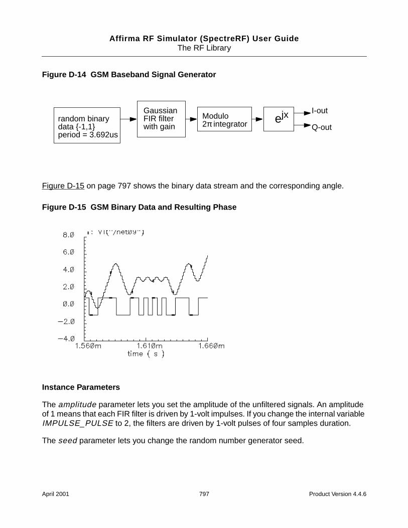
Affirma RF Simulator (SpectreRF) User GuideThe RF Library
Figure D-14 GSM Baseband Signal Generator
Figure D-15 on page 797 shows the binary data stream and the corresponding angle.
Figure D-15 GSM Binary Data and Resulting Phase
Instance Parameters
The amplitude parameter lets you set the amplitude of the unfiltered signals. An amplitudeof 1 means that each FIR filter is driven by 1-volt impulses. If you change the internal variableIMPULSE_PULSE to 2, the filters are driven by 1-volt pulses of four samples duration.
The seed parameter lets you change the random number generator seed.
random binarydata -1,1
GaussianFIR filter Modulo
2π integratorwith gainejx I-out
period = 3.692usQ-out
April 2001 797 Product Version 4.4.6
Affirma RF Simulator (SpectreRF) User GuideThe RF Library
Outputs
The generator creates four output signals
Changing the FIR Filter
You cannot change the FIR filter, such as the tap length and tap coefficients, directly from theinstance. However, you can do so using the Modelwriter as described in “Creating Variationson the Library Baseband Signal Generators Using the Modelwriter” on page 801.
Output Transitions
The filtered outputs slew linearly from one value to the next because the rise and fall times inthe transition statements equal one period. To make the outputs take abrupt steps, copy themodule to your library and change the rise and fall times in the last transition statements.
Π/4-DQPSK Signal Source (pi_over4_dqpsk)
Figure D-16 shows the block diagram for this source and Table D-1 on page 799 shows howthe phase shift is generated.
angular_node The output signal.
i_out_node The phase, multiplied by the amplitude.
bin_node The bit stream being transmitted.
q_out_node The phase multiplied by the amplitude.
April 2001 798 Product Version 4.4.6
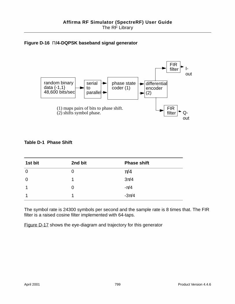
Affirma RF Simulator (SpectreRF) User GuideThe RF Library
Figure D-16 Π/4-DQPSK baseband signal generator
Table D-1 Phase Shift
The symbol rate is 24300 symbols per second and the sample rate is 8 times that. The FIRfilter is a raised cosine filter implemented with 64-taps.
Figure D-17 shows the eye-diagram and trajectory for this generator
1st bit 2nd bit Phase shift
0 0 π/40 1 3π/4
1 0 -π/4
1 1 -3π/4
random binarydata -1,148,600 bits/sec
differentialencoder
FIRfilter
FIRfilter
I-out
Q-out
phase statecoder (1)
serialtoparallel
(1) maps pairs of bits to phase shift.(2) shifts symbol phase.
(2)
April 2001 799 Product Version 4.4.6
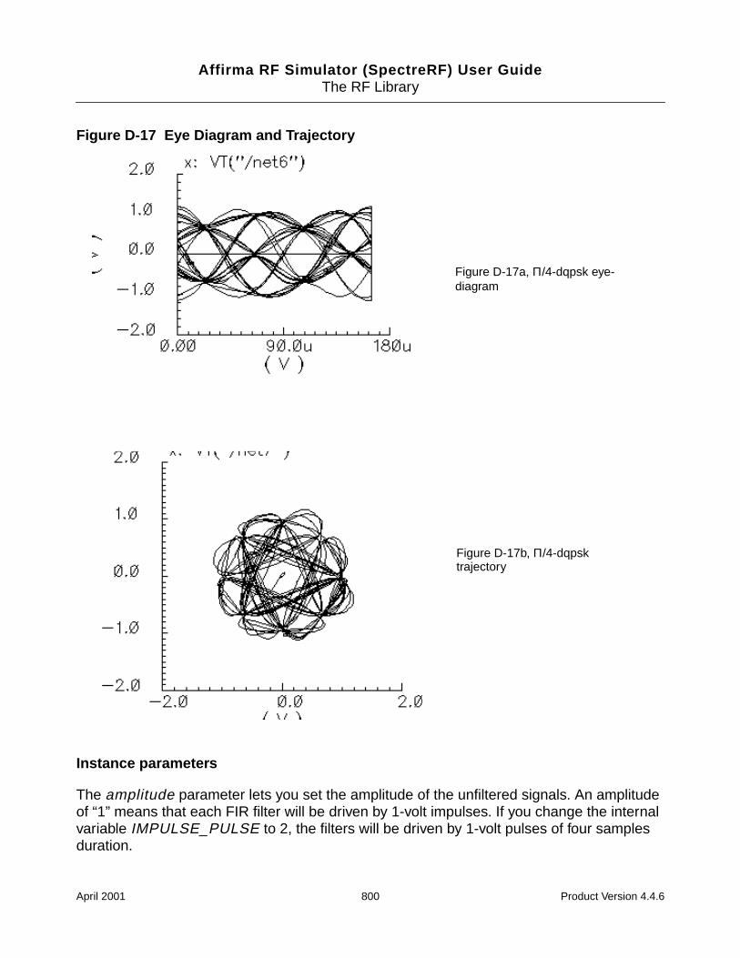
Affirma RF Simulator (SpectreRF) User GuideThe RF Library
Figure D-17 Eye Diagram and Trajectory
Instance parameters
The amplitude parameter lets you set the amplitude of the unfiltered signals. An amplitudeof “1” means that each FIR filter will be driven by 1-volt impulses. If you change the internalvariable IMPULSE_PULSE to 2, the filters will be driven by 1-volt pulses of four samplesduration.
Figure D-17a, Π/4-dqpsk eye-diagram
Figure D-17b, Π/4-dqpsktrajectory
April 2001 800 Product Version 4.4.6
Affirma RF Simulator (SpectreRF) User GuideThe RF Library
The seed parameter lets you change the random number generator seed.
Outputs
The generator creates four output signals.
Changing the FIR filter
You cannot change the FIR filter, such as the tap length and tap coefficients, directly from theinstance. However, you can do so using the Modelwriter as described in “Creating Variationson the Library Baseband Signal Generators Using the Modelwriter” on page 801.
Output transitions
The filtered outputs slew linearly from one value to the next because the rise and fall times inthe transition statements equal one period. To make the outputs take abrupt steps, copy themodule to your library and change the rise and fall times in the last transition statements.
Creating Variations on the Library Baseband Signal Generators Using theModelwriter
The baseband signal generators use FIR filters to shape their output pulses. Shaped outputpulses serve several purposes:
They help keep the transmitted signal inside the specified band.
They work with their receive counterparts to maximize the signal-to-noise ratio.
Together with their receiver counterparts, they satisfy the Nyquist sampling criterion foran intersymbol-interference-free channel.
The Modelwriter gives you a convenient user-interface for creating variations on thebaseband signal generators in the library. The most likely variation is in the FIR filter. Thissection explains how to use the Model Writer to create a new GSM generator with differentFIR filters.
i_out_node The phase, multiplied by the amplitude.
q_out_node The phase, multiplied by the amplitude.
phase_shift_out The phase shift from one symbol to the next.
April 2001 801 Product Version 4.4.6
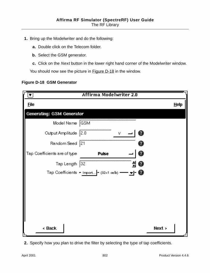
Affirma RF Simulator (SpectreRF) User GuideThe RF Library
1. Bring up the Modelwriter and do the following:
a. Double click on the Telecom folder.
b. Select the GSM generator.
c. Click on the Next button in the lower right hand corner of the Modelwriter window.
You should now see the picture in Figure D-18 in the window.
Figure D-18 GSM Generator
2. Specify how you plan to drive the filter by selecting the type of tap coefficients.
April 2001 802 Product Version 4.4.6

Affirma RF Simulator (SpectreRF) User GuideThe RF Library
FIR filters can be driven by pulses or impulses.
3. Specify the length of the FIR filter in the Tap Length field.
4. You can specify the tap coefficients in two ways
From a file
By direct manual entry.
To read the coefficients from a file do the following:
a. Select the Import button.
b. Enter the path to the file.
c. Click on Open.
The coefficients appear in the window as shown in Figure D-19 on page 804. (The tap[1]coefficient multiplies the filter state with the least amount of delay, the filter state closestto the input.)
To enter the coefficients manually do the following:
a. Click on the lower rightmost button flagged in the form.
See Figure D-20 on page 805.
b. Enter the coefficients,
c. Click next to view the model,
d. To write the model to a file, click Save Generated Code....
April 2001 803 Product Version 4.4.6
Affirma RF Simulator (SpectreRF) User GuideThe RF Library
Figure D-19 Tap coefficients
April 2001 804 Product Version 4.4.6
Affirma RF Simulator (SpectreRF) User GuideThe RF Library
Figure D-20 Manual entry of the tap coefficients
Uncatagorized Elements
The rfLib contains the following uncatagorized elements:
cdma_2ms_idata
cdma_2ms_qdata
dqpsk_20ms_idata
Click here
April 2001 805 Product Version 4.4.6

Affirma RF Simulator (SpectreRF) User GuideThe RF Library
dqpsk_20ms_qdata
gsm_5ms_idata
gsm_5ms_qdata
All of these elements are files generated by elements of the Testbench category described in“Testbench Elements” on page 793.
April 2001 806 Product Version 4.4.6
Affirma RF Simulator (SpectreRF) User Guide
EPlotting Spectre S-Parameter SimulationData
The procedures described in this appendix are deliberately broad and generic. Requirementsfor your specific design might dictate procedures slightly different from those described here.
This appendix describes the equations used by the Spectre S-Parameter WaveformCalculator.
The Equations for the S-Parameter Waveform Calculator in the AffirmaAnalog Circuit Design Environment:
Using the Waveform Calculator in the Affirma analog circuit design environment, you can plotthe following S-parameter data:
Network parameters
Two-port scalar quantities
Two-port gain quantities
Two-port network circles
Voltage standing wave ratio
Group delay
On the S-Parameter Results form, buttons in the Function area specify the type of data to plot.
Network Parameters: S, Z, Y, or H parameters
S, Y, and Z parameters (denoted as SP, ZP, YP, and HP on the Plot form) are defined forcircuits with any number of ports. H-parameters (HP) are defined for only two-port circuits.
April 2001 807 Product Version 4.4.6
Affirma RF Simulator (SpectreRF) User GuidePlotting Spectre S-Parameter Simulation Data
You can plot the parameters on polar charts, Smith charts, or on a rectangular plot afterapplying one of the Modifier options. The dB conversion uses 20log10x, because theparameters represent scalar (for example, voltage) ratios.
For the ZP, YP, and HP parameters, Spectre returns S-parameters to the Affirma analogcircuit design environment. The environment converts them, as needed, to the equivalent Z,Y, and H matrices using standard published methods.
The network parameter calculations:
SP (S-parameter) values are calculated by Spectre
ZP (Z-parameter) equations
where
Sm is the N-port S-parameter matrix
I is the N x N identity matrix
Zref is a diagonal matrix defined as
where
Zi is the terminating impedance at port i
Zm is the resulting Z-parameter matrix
YP (Y-parameter) equation
where
Sm is the N-port S-parameter matrix
I is the N x N identity matrix
Yref is a diagonal matrix defined as
Zm Zref[ ] I Sm–[ ] I Sm+[ ] 1–Zref[ ]=
Zref SQRT ℜe Zi ( )=
Ym Yref[ ] I Sm–[ ] I Sm+[ ] 1–Yref[ ]=
Yref1
SQRT ℜe Zi ( )-----------------------------------------=
April 2001 808 Product Version 4.4.6
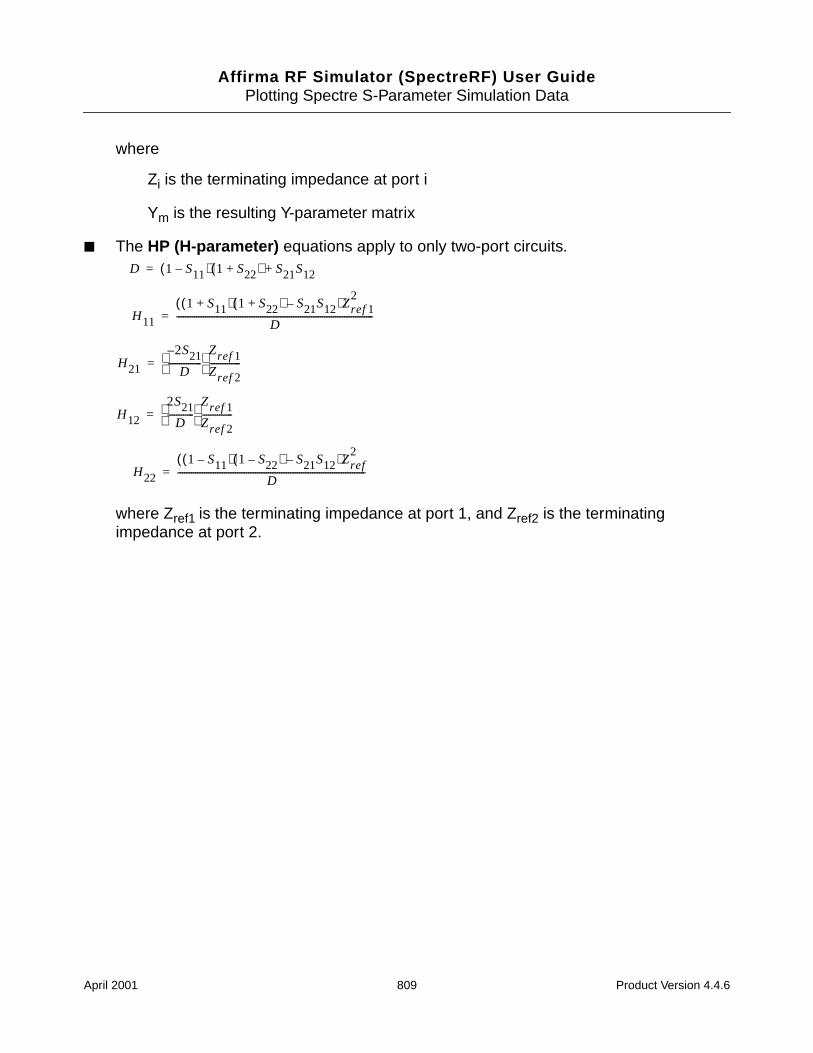
Affirma RF Simulator (SpectreRF) User GuidePlotting Spectre S-Parameter Simulation Data
where
Zi is the terminating impedance at port i
Ym is the resulting Y-parameter matrix
The HP (H-parameter) equations apply to only two-port circuits.
where Zref1 is the terminating impedance at port 1, and Zref2 is the terminatingimpedance at port 2.
D 1 S11–( ) 1 S22+( ) S21S12+=
H11
1 S11+( ) 1 S22+( ) S21S12–( )Zref 12
D-----------------------------------------------------------------------------------------=
H21
2S21–
D---------------
Zref 1Zref 2--------------=
H12
2S21D
------------ Zref 1
Zref 2--------------=
H22
1 S11–( ) 1 S22–( ) S21S12–( )Zref2
D-------------------------------------------------------------------------------------=
April 2001 809 Product Version 4.4.6
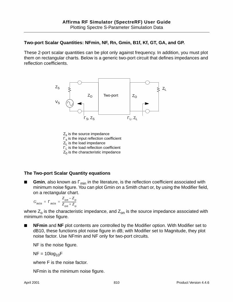
Affirma RF Simulator (SpectreRF) User GuidePlotting Spectre S-Parameter Simulation Data
Two-port Scalar Quantities: NFmin, NF, Rn, Gmin, B1f, Kf, GT, GA, and GP.
These 2-port scalar quantities can be plot only against frequency. In addition, you must plotthem on rectangular charts. Below is a generic two-port circuit that defines impedances andreflection coefficients.
The Two-port Scalar Quantity equations
Gmin , also known as Γmin in the literature, is the reflection coefficient associated withminimum noise figure. You can plot Gmin on a Smith chart or, by using the Modifier field,on a rectangular chart.
where Zo is the characteristic impedance, and Zon is the source impedance associated withminimum noise figure.
NFmin and NF plot contents are controlled by the Modifier option. With Modifier set todB10, these functions plot noise figure in dB; with Modifier set to Magnitude, they plotnoise factor. Use NFmin and NF only for two-port circuits.
NF is the noise figure.
NF = 10log10F
where F is the noise factor.
NFmin is the minimum noise figure.
Zs is the source impedanceΓs is the input reflection coefficientZL is the load impedanceΓL is the load reflection coefficientZ0 is the characteristic impedance
Two-port
ΓS, ZS ΓL, ZL
ZS
VS
ZL
ZO ZO
Gmin Γmin
Zon Zo–
Zon Zo+----------------------= =
April 2001 810 Product Version 4.4.6
Affirma RF Simulator (SpectreRF) User GuidePlotting Spectre S-Parameter Simulation Data
The NFmin values are calculated by Spectre
The NF (noise figure) equation is calculated by the Affirma analog circuit designenvironment from NFmin, Gmin (Γmin), and rn. You can specify the optional sourcereflection coefficient ΓS as an argument if you use the design environment calculator.From the direct plot form, The environment assumes ΓS to be 0 (input matched toreference termination).
Where r n = R n/Z o and rn is the normalized equivalent noise resistance.
Rn (equivalent noise resistance) plots equivalent noise resistance. The Rn values arecalculated by Spectre.
Stability Factors
Kf and B1f plot the Rollet stability factor and its intermediate term. Use these parametersonly for two-port circuits.
Two-port gain quantities: GA, GP, GT, Gumx, Gmax, and Gmsg.
The following gain quantities are valid only for two-port circuits
GA (available gain) is the power gain obtained by optimally matching the output of thenetwork.
GP (power gain) is the power gain obtained by optimally matching the input of the network.
GT (transducer gain) shows the insertion effect of a two-port circuit (used in amplifierdesign).
Gumx (maximum unilateral transducer power gain)
NF NFmin
4rn ΓS Γmin–2
1 ΓS2
1 Γmin+2
–( )------------------------------------------------------+=
D S11S22 S21S12–=
K f
1 S112
– S222
– D2
+
2 S21 S12------------------------------------------------------------=
B1 f
1 S112
S222
– D2
+ +
2 S11 S22∗D–
-------------------------------------------------------------=
April 2001 811 Product Version 4.4.6
Affirma RF Simulator (SpectreRF) User GuidePlotting Spectre S-Parameter Simulation Data
Gmax (maximum available gain) shows the transducer power gain when there exists asimultaneous conjugate match at both ports.
Gmsg (maximum stable gain) shows the gain that can be achieved by resistively loadingthe 2 port such that k=1 and then simultaneously conjugately matching the input and outputports. For conditionally stable 2-ports, you can approach the maximum stable gain as youreduce the input and output mismatch. If you attempt a simultaneous conjugate match andk<1, the 2-port will oscillate.
Two-port Gain Calculations
GA (available gain) equations (output conjugately matched)
where
Note: When you use the S-parameter Results direct plot form, GS is set to zero, andtherefore available gain (GA) is plotted as
To plot GA for nonzero values of GS, use the design environment calculator.
GP (power gain) equations (input conjugately matched)
GA
S212
1 ΓS2
–( )
1 S11ΓS–2
1 Γ22
–( )---------------------------------------------------------=
Γ2 S22
S12S21ΓS1 S11ΓS–------------------------+=
GA
S212
1 S222
–-----------------------=
GP
S212
1 ΓL2
–( )
1 S22ΓL–2
1 Γ12
–( )---------------------------------------------------------=
April 2001 812 Product Version 4.4.6
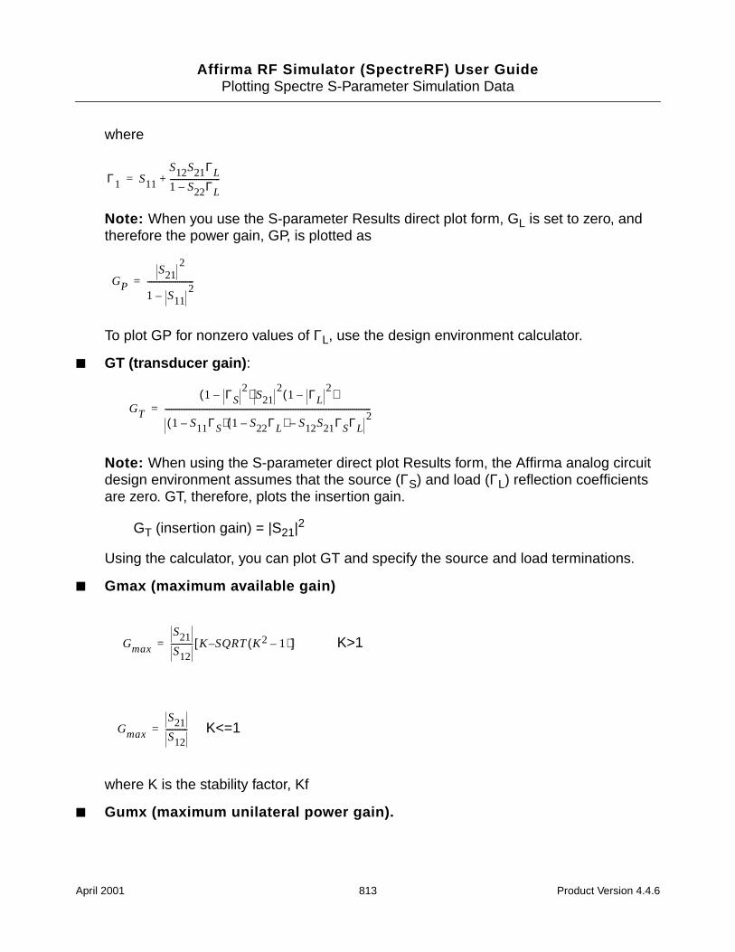
Affirma RF Simulator (SpectreRF) User GuidePlotting Spectre S-Parameter Simulation Data
where
Note: When you use the S-parameter Results direct plot form, GL is set to zero, andtherefore the power gain, GP, is plotted as
To plot GP for nonzero values of ΓL, use the design environment calculator.
GT (transducer gain) :
Note: When using the S-parameter direct plot Results form, the Affirma analog circuitdesign environment assumes that the source (ΓS) and load (ΓL) reflection coefficientsare zero. GT, therefore, plots the insertion gain.
GT (insertion gain) = |S21|2
Using the calculator, you can plot GT and specify the source and load terminations.
Gmax (maximum available gain)
K>1
K<=1
where K is the stability factor, Kf
Gumx (maximum unilateral power gain).
Γ1 S11
S12S21ΓL1 S22ΓL–-------------------------+=
GP
S212
1 S112
–-----------------------=
GT
1 ΓS2
–( ) S212
1 ΓL2
–( )
1 S11ΓS–( ) 1 S22ΓL–( ) S12S21ΓSΓL–2
-------------------------------------------------------------------------------------------------------=
Gmax
S21S12----------- K S– QRT K2 1–( )[ ]=
Gmax
S21S12-----------=
April 2001 813 Product Version 4.4.6
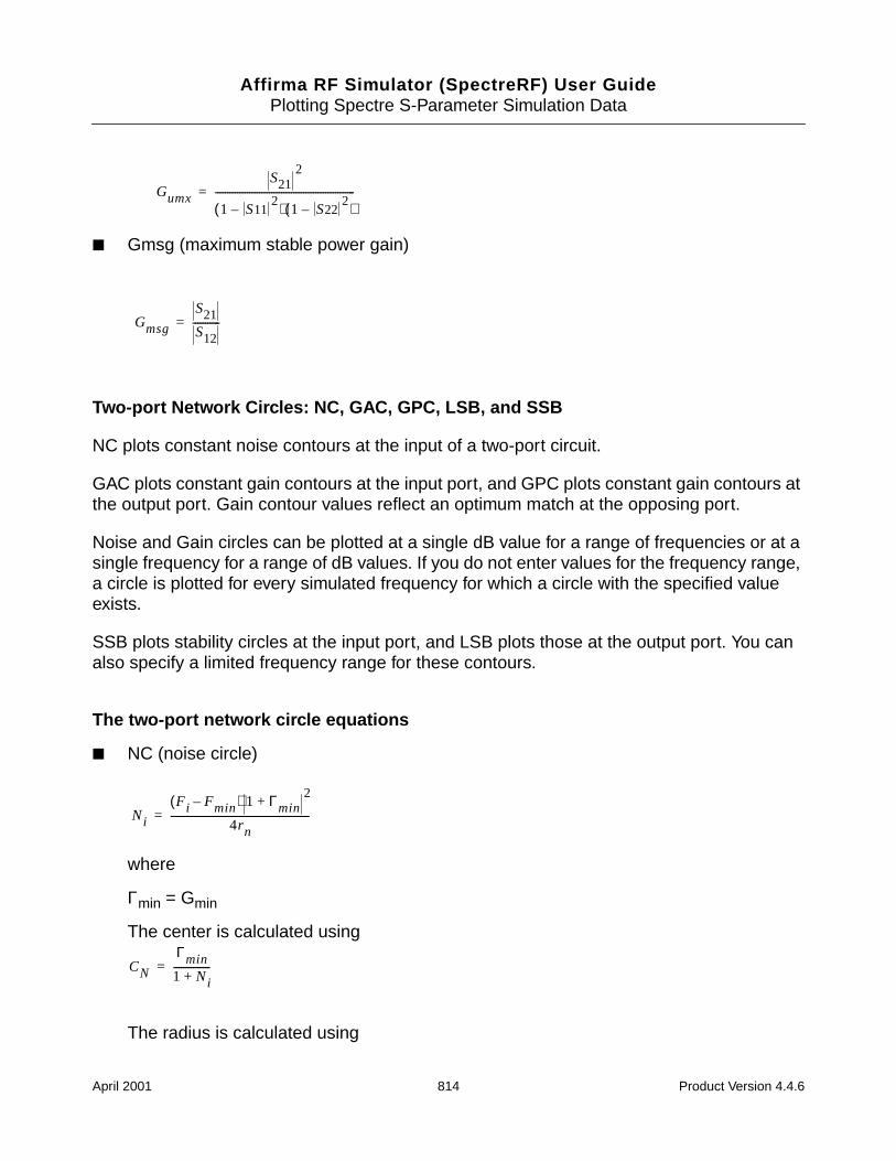
Affirma RF Simulator (SpectreRF) User GuidePlotting Spectre S-Parameter Simulation Data
Gmsg (maximum stable power gain)
Two-port Network Circles: NC, GAC, GPC, LSB, and SSB
NC plots constant noise contours at the input of a two-port circuit.
GAC plots constant gain contours at the input port, and GPC plots constant gain contours atthe output port. Gain contour values reflect an optimum match at the opposing port.
Noise and Gain circles can be plotted at a single dB value for a range of frequencies or at asingle frequency for a range of dB values. If you do not enter values for the frequency range,a circle is plotted for every simulated frequency for which a circle with the specified valueexists.
SSB plots stability circles at the input port, and LSB plots those at the output port. You canalso specify a limited frequency range for these contours.
The two-port network circle equations
NC (noise circle)
where
Γmin = Gmin
The center is calculated using
The radius is calculated using
Gumx
S212
1 S112
–( ) 1 S222
–( )---------------------------------------------------------=
Gmsg
S21S12-----------=
Ni
Fi Fmin–( ) 1 Γmin+2
4rn---------------------------------------------------------=
CN
Γmin1 Ni+---------------=
April 2001 814 Product Version 4.4.6
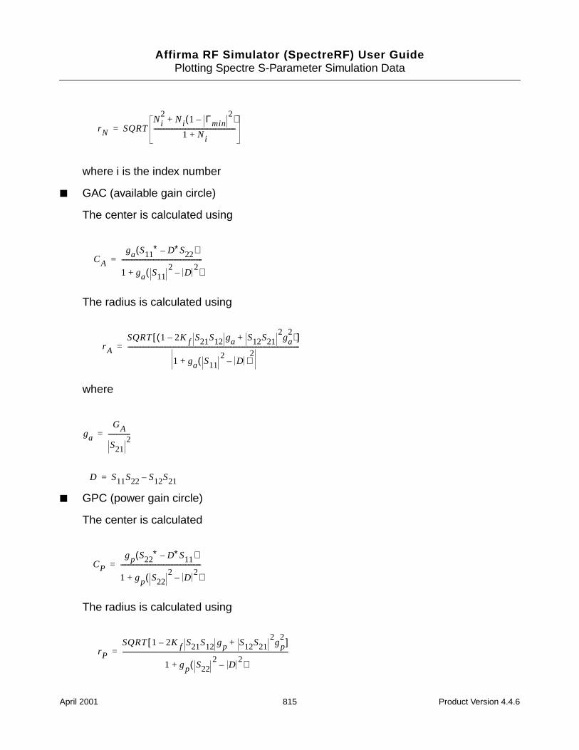
Affirma RF Simulator (SpectreRF) User GuidePlotting Spectre S-Parameter Simulation Data
where i is the index number
GAC (available gain circle)
The center is calculated using
The radius is calculated using
where
GPC (power gain circle)
The center is calculated
The radius is calculated using
r N SQRTNi
2Ni 1 Γmin
2–( )+
1 Ni+----------------------------------------------------=
CA
ga S11∗ D∗S22–( )
1 ga S112
D2
–( )+
---------------------------------------------------=
r A
SQRT 1 2K f S21S12 ga– S12S212ga
2+( )[ ]
1 ga S112
D–( )2
+
-------------------------------------------------------------------------------------------------------------=
ga
GA
S212
--------------=
D S11S22 S12S21–=
CP
gp S22∗ D∗S11–( )
1 gp S222
D2
–( )+
---------------------------------------------------=
rP
SQRT 1 2K f S21S12 gp– S12S212gp
2+[ ]
1 gp S222
D2
–( )+
---------------------------------------------------------------------------------------------------------=
April 2001 815 Product Version 4.4.6
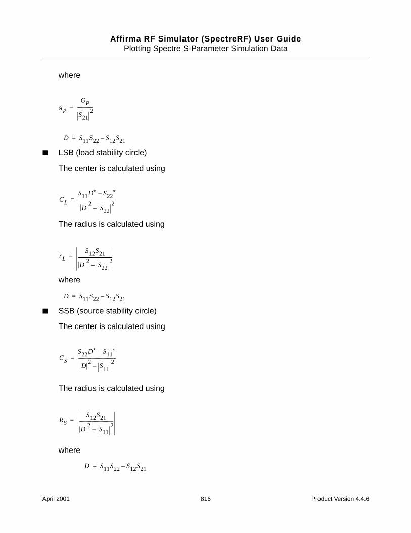
Affirma RF Simulator (SpectreRF) User GuidePlotting Spectre S-Parameter Simulation Data
where
LSB (load stability circle)
The center is calculated using
The radius is calculated using
where
SSB (source stability circle)
The center is calculated using
The radius is calculated using
where
gp
GP
S212
--------------=
D S11S22 S12S21–=
CL
S11D∗ S22∗–
D2
S222
–----------------------------------=
rLS12S21
D2
S222
–------------------------------=
D S11S22 S12S21–=
CS
S22D∗ S11∗–
D2
S112
–----------------------------------=
RSS12S21
D2
S112
–------------------------------=
D S11S22 S12S21–=
April 2001 816 Product Version 4.4.6
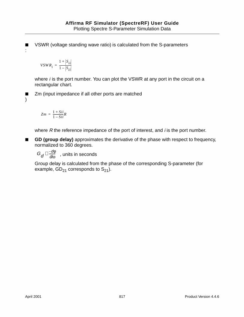
Affirma RF Simulator (SpectreRF) User GuidePlotting Spectre S-Parameter Simulation Data
VSWR (voltage standing wave ratio) is calculated from the S-parameters:
where i is the port number. You can plot the VSWR at any port in the circuit on arectangular chart.
Zm (input impedance if all other ports are matched)
where R the reference impedance of the port of interest, and i is the port number.
GD (group delay) approximates the derivative of the phase with respect to frequency,normalized to 360 degrees.
, units in seconds
Group delay is calculated from the phase of the corresponding S-parameter (forexample, GD21 corresponds to S21).
VSW Ri1 Sii+
1 Sii–------------------=
Zm1 Sii+1 Sii–----------------R=
Gddφ–
dω--------≅
April 2001 817 Product Version 4.4.6
Affirma RF Simulator (SpectreRF) User Guide
FUsing Pdisto Analysis Effectively
Periodic Distortion (Pdisto) analysis computes the steady-state responses of circuits withmultiple periodic inputs of differing frequencies. The Pdisto mixed frequency-time (MFT)approach is more efficient than transient circuit simulation when inputs are stiff (with largetime constants). MFT also performs better than traditional algorithms such as harmonicbalance when solving highly nonlinear problems. A typical application of Pdisto is to predictthe harmonic distortion of switched-capacitor filters that operate under widely separatedfundamentals (see an example in “Switched Capacitor Filter Example” on page 826).
Pdisto can also predict intermodulation distortion of a narrowband circuit that is driven by aLO and two high-frequency input fundamentals that are closely spaced in frequency, such asin the down conversion stage at a receiver, (see an example in “High-Performance ReceiverExample” on page 827).
This Appendix contains the following:
A discussion of when to use Pdisto analysis
A brief description of the MFT method
A comparison of Pdisto and PSS analyses
A comparison of Pdisto and PAC analyses
Two examples of typical use: a switched capacitor filter and a high-performance receiver
Procedures for setting up and running Pdisto analysis
When to Use Pdisto Analysis
The increasing demand for low-cost, mobile communication systems increases the need forefficient and accurate simulation algorithms for RF communication circuits. These circuits aredifficult to simulate because they process modulated carrier signals that consist of a highfrequency carrier and a low frequency modulation signal. Typically, the carrier frequencyranges from 1-5 GHz and the modulation from 10 kHz to 1 MHz. Applying standard transientanalysis to such circuits might require simulating the detailed response of the circuit over
April 2001 818 Product Version 4.4.6
Affirma RF Simulator (SpectreRF) User GuideUsing Pdisto Analysis Effectively
hundreds of thousands of clock cycles (millions of timepoints), a generally impracticalapproach.
Fortunately, many circuits of interest operate near a time-varying, but periodic, operatingpoint. Some of these circuits can be analyzed if you assume that one of the circuit inputsproduces a periodic response that you can calculate using PSS analysis. Other time-varyingcircuit inputs are then treated as small signals by linearizing the circuit around the periodicoperating point, and you can analyze small signals efficiently using the SpectreRF PeriodicAC (PAC) analysis [8]. This approach lets you avoid long simulation times with transientanalysis[7].
However, many circuits cannot be analyzed efficiently with this periodic-operating-point-plus-small-signal approach. For example, predicting the intermodulation distortion of anarrowband circuit, such as a receiver down converter (a mixer followed by a filter), requirescalculating the nonlinear response of the mixer circuit, driven by a LO, to two closely spacedhigh-frequency inputs. The response to both inputs is within the band width of the filter. Thesteady-state response of such a circuit is quasi-periodic.
As a further complication, many multi-timescale circuits, such as mixers and switched-capacitor filters, have a highly nonlinear response with respect to one or more of the excitinginputs. Consequently, steady-state approaches such as multi-frequency harmonic balancedo not perform well.
Mixed frequency-time (MFT) approaches avoid these difficulties. They assume that manycircuits of engineering interest have a strongly nonlinear response to only one input, such asthe clock in a switched-capacitor circuit or the LO in a mixer, and respond in a weaklynonlinear manner to other inputs.
Compared to previous MFT methods [2, 4], the Pdisto algorithm has many of the followingadvantages:
MFT methods avoid the ill-conditioning caused by a poor choice of boundary conditionsfound in previous algorithms
MFT methods use a multi-dimensional discrete Fourier transform (DFT) for cycleplacement
MFT methods use a continuation method to enhance the global convergence ofNewton’s method
MFT methods use a matrix-implicit, Krylov-subspace-based iterative scheme that letsMFT methods solve large problems
MFT methods have a preconditioning strategy that permit the iterative solver to rapidconverge
April 2001 819 Product Version 4.4.6
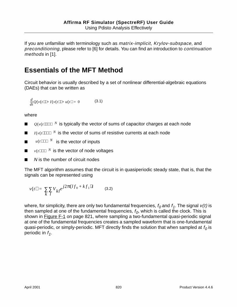
Affirma RF Simulator (SpectreRF) User GuideUsing Pdisto Analysis Effectively
If you are unfamiliar with terminology such as matrix-implicit, Krylov-subspace, andpreconditioning, please refer to [6] for details. You can find an introduction to continuationmethods in [1].
Essentials of the MFT Method
Circuit behavior is usually described by a set of nonlinear differential-algebraic equations(DAEs) that can be written as
where
is typically the vector of sums of capacitor charges at each node
is the vector of sums of resistive currents at each node
is the vector of inputs
is the vector of node voltages
N is the number of circuit nodes
The MFT algorithm assumes that the circuit is in quasiperiodic steady state, that is, that thesignals can be represented using
where, for simplicity, there are only two fundamental frequencies, f0 and f1. The signal v(t) isthen sampled at one of the fundamental frequencies, f0, which is called the clock. This isshown in Figure F-1 on page 821, where sampling a two-fundamental quasi-periodic signalat one of the fundamental frequencies creates a sampled waveform that is one-fundamentalquasi-periodic, or simply-periodic. MFT directly finds the solution that when sampled at f0 isperiodic in f1.
ddt-----Q v t( )( ) I v t( )( ) u t( )+ + 0= (3.1)
Q v t( )( ) ℜN∈
I v t( )( ) ℜN∈
u t( ) ℜN∈
v t( ) ℜN∈
v t( ) Vklej2π l f 0 k f 1+( )t
l∑
k∑= (3.2)
April 2001 820 Product Version 4.4.6
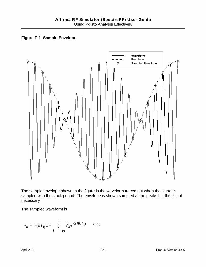
Affirma RF Simulator (SpectreRF) User GuideUsing Pdisto Analysis Effectively
Figure F-1 Sample Envelope
The sample envelope shown in the figure is the waveform traced out when the signal issampled with the clock period. The envelope is shown sampled at the peaks but this is notnecessary.
The sampled waveform is
vn v nT0( ) Vkej2πk f 1t
k ∞–=
∞∑= = (3.3)
April 2001 821 Product Version 4.4.6
Affirma RF Simulator (SpectreRF) User GuideUsing Pdisto Analysis Effectively
where T0 = 1/f0. Alternatively, you can write
which states that is the inverse Fourier transform of .
Recall that v is a solution of the circuit equations, and that is simply v uniformly sampled,so given one can compute a subsequent sample point using
where
ϕ is the state transition function for the circuit.
ϕ(v0, t0, t1) is the solution for the circuit equations at t1, given that it starts from the initialcondition v0 at t0.
Consider the nth sample interval. Then let be the solution at the start of the intervaland be the solution at the end. Then (3.5) uses the circuit equations torelate the solution at both ends of the interval,
Let X = Fx and Y = Fy (X and Y are the Fourier transforms of x and y). Then, from (3.3) andbecause yn = xn+1,
or
where is a diagonal delay matrix with being the kth diagonal element.
Together, (3.6) and (3.8) make up the MFT method.
In practice, is band-limited, so only a finite number of harmonics are needed. Inaddition, if the circuit is driven with one large high-frequency signal at f0, which is called theclock, and one moderately-sized sinusoid at f1, only K harmonics are needed and themethod is efficient. With only K harmonics, (3.6) is evaluated over 2K+1 distinct intervals that
vn F 1– V= (3.4)
v V
v
vn vn 1+
vn 1+ φ vn nT0 n 1+( )T0, ,( )= (3.5)
xn vn=
yn vn 1+ xn 1+= =
yn φ vn nT0 n 1+( )T0, ,( )= (3.6)
Xk e j2πk f 1T0– Yk= (3.7)
X DT0Y= (3.8)
DT0e j2πk f 1T0–
V X=
April 2001 822 Product Version 4.4.6
Affirma RF Simulator (SpectreRF) User GuideUsing Pdisto Analysis Effectively
are spread evenly over one period of the lowest beat tone. Therefore, the total simulation timeis proportional to the number of harmonics needed to represent the sampled waveform. Thesimulation time is independent of the period of the lowest-frequency beat tone or theharmonics needed to represent the clock signal.
Equation (3.8), along with the associated Fourier transforms, relate the starting and endingpoints of the solution of the circuit equations over each interval, and consequently representa boundary-value constraint on (3.6).
Shooting methods are the most common method for solving boundary-value problems. Theiruse of transient analysis to solve the circuit equations over an interval brings two importantbenefits.
First, transient analysis handles abruptly discontinuous signals efficiently because thetimestep shrinks to follow rapid transitions.
Second, transient analysis easily handles the strongly nonlinear behavior of the circuitas it responds to the large clock signal.
Pdisto and PSS Analyses Compared
Like PSS, Pdisto uses a shooting Newton method. However, instead of doing a singletransient integration, each Newton iteration does transient integrations over a number of non-adjacent clock periods. Each of the integrations differs by a phase-shift in each moderateinput signal. The number of integrations is determined by the numbers of harmonics ofmoderate fundamentals that you specify. Given maxharms = [k1, k2, ..., kS], the totalnumber of integrations is
Consequently, the efficiency of the algorithm depends significantly on the number ofharmonics required to model the responses of moderate fundamentals.
Fortunately, the number of harmonics of the clock does not significantly affect the efficiencyof the shooting algorithm. The boundary conditions of a shooting interval are such that thetime-domain integrations are consistent with a frequency-domain transformation with a shiftof one large-signal period.
As a SpectreRF user, you might need to run PSS to calculate the steady-state operating pointof circuits with multiple input frequencies. You can do this by using the greatest commonfactor of all input frequencies as the PSS beat frequency.
2ks 1+( )s 1=
S
∏
April 2001 823 Product Version 4.4.6
Affirma RF Simulator (SpectreRF) User GuideUsing Pdisto Analysis Effectively
When the greatest common factor is relatively close to the clock frequency, such as within afactor of 10, PSS might be preferable to Pdisto for two reasons.
First each nonlinear iteration would not require excessive integrations of clock period.
Second, PSS solves a much smaller linear system in each nonlinear iteration.
The size of the linear system resulting from Pdisto analysis is
times as big as that of PSS analysis.
In general,
If the clock/beat frequency ratio of PSS is smaller than K, PSS might be preferable toPdisto.
For circuits operating on wide timescales, such as switched-capacitor filters, the clock/beat frequency of PSS can be greater than 1000, and Pdisto is clearly the method ofchoice.
Another difference between the two analyses is that PSS does not have any restrictions oninput sources, whereas Pdisto requires that all non-clock inputs must be sinusoidal.
One limitation of the current Pdisto analysis is that small signal analyses after Pdisto, suchas quasi-periodic noise analysis, cannot be performed.
Pdisto analysis also cannot currently be applied to autonomous circuits.
Pdisto and PAC Analyses Compared
Like PAC analysis, the Pdisto analysis calculates responses of a circuit that exhibitsfrequency translations. However, instead of having small-signal linear behavior, Pdistomodels the response as having components of a few harmonics of input-signal frequencies.This permits computing responses to moderately large input signals.
PAC analysis assumes that only the clock is generating harmonics. For example, for a clockfrequency fc, and a small signal frequency fs, amplitudes of circuit response are generatedat fs kc fc, where kc is bonded by the parameter harms in PSS analysis. In contrast, Pdistoalso permits non-clock fundamentals to generate harmonics. In the same situation, a
K 2ks 1+( )s 1=
S
∏=
April 2001 824 Product Version 4.4.6

Affirma RF Simulator (SpectreRF) User GuideUsing Pdisto Analysis Effectively
spectrum at frequencies ksfs kcfc is generated, where ks and kc are bonded by the Pdistoparameter maxharms.
Unlike PAC, a PSS analysis is not explicitly required before a Pdisto analysis. Pdisto internallyruns a PAC analysis to determine initial conditions.
Pdisto Analysis Parameters
While Pdisto analysis inherits most PSS parameters, it adds two new parameters
funds
maxharms
These two parameters replace the PSS parameters, fund (or period) and harms,respectively.
The funds parameter accepts a list of names of fundamentals that are present in the sources.These names are specified in the sources by parameter fundname. The first fundamental isassumed to be the large signal.
The maxharms parameter accepts a list of numbers of harmonics needed for eachfundamental.
If you do not list all the fundamental names using the funds parameter, the current analysisis skipped. However, if you do not specify maxharms, a warning message is issued, and thenumber of harmonics is defaulted to 1 for each of the fundamentals.
The remaining Pdisto analysis parameters are inherited directly from PSS analysis, and theirmeanings remain essentially unchanged.
Pdisto analysis expands the role of some PSS parameters. The maxperiods parameter thatcontrols the maximum number of shooting iterations for PSS analysis also controls thenumber of the maximum number of shooting iterations for Pdisto analysis.
Application Examples
Pdisto analysis is particularly efficient for circuits operating on widely separated timescales.This is demonstrated by the following two examples
A switched capacitor filter
A high-performance receiver
April 2001 825 Product Version 4.4.6
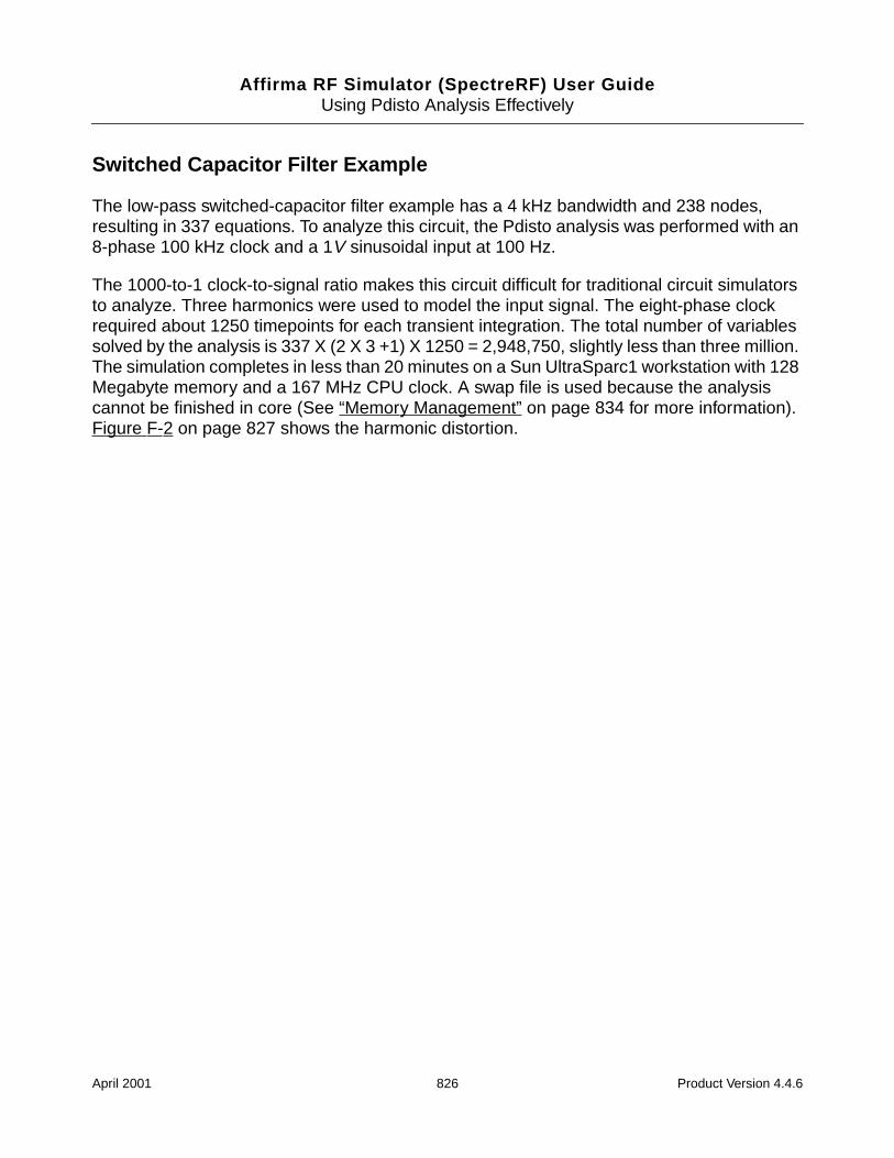
Affirma RF Simulator (SpectreRF) User GuideUsing Pdisto Analysis Effectively
Switched Capacitor Filter Example
The low-pass switched-capacitor filter example has a 4 kHz bandwidth and 238 nodes,resulting in 337 equations. To analyze this circuit, the Pdisto analysis was performed with an8-phase 100 kHz clock and a 1V sinusoidal input at 100 Hz.
The 1000-to-1 clock-to-signal ratio makes this circuit difficult for traditional circuit simulatorsto analyze. Three harmonics were used to model the input signal. The eight-phase clockrequired about 1250 timepoints for each transient integration. The total number of variablessolved by the analysis is 337 X (2 X 3 +1) X 1250 = 2,948,750, slightly less than three million.The simulation completes in less than 20 minutes on a Sun UltraSparc1 workstation with 128Megabyte memory and a 167 MHz CPU clock. A swap file is used because the analysiscannot be finished in core (See “Memory Management” on page 834 for more information).Figure F-2 on page 827 shows the harmonic distortion.
April 2001 826 Product Version 4.4.6
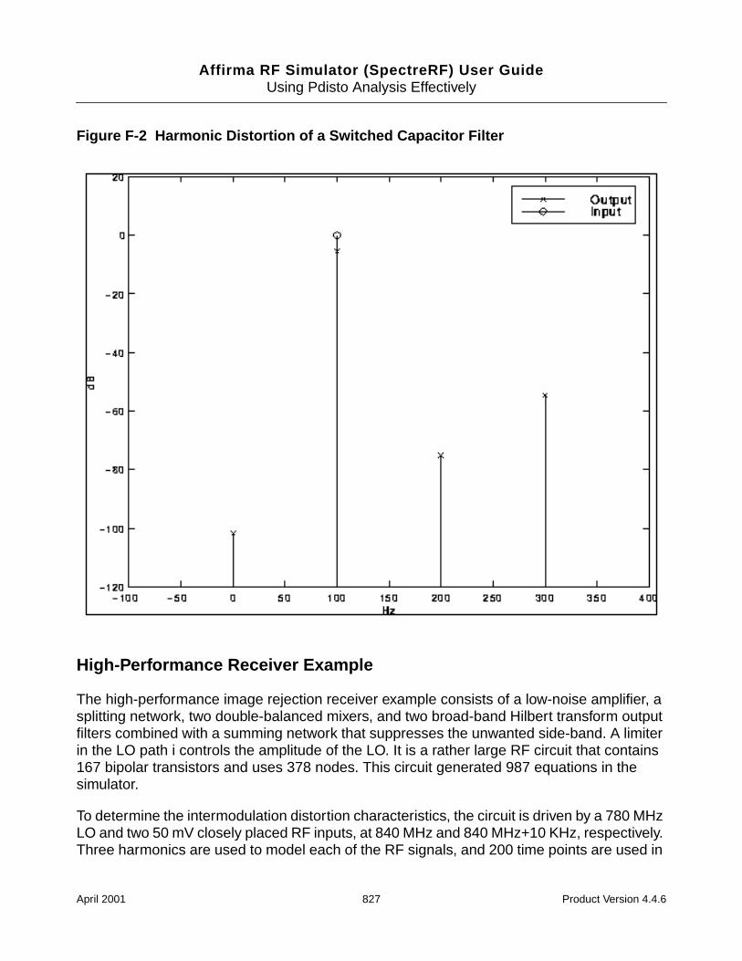
Affirma RF Simulator (SpectreRF) User GuideUsing Pdisto Analysis Effectively
Figure F-2 Harmonic Distortion of a Switched Capacitor Filter
High-Performance Receiver Example
The high-performance image rejection receiver example consists of a low-noise amplifier, asplitting network, two double-balanced mixers, and two broad-band Hilbert transform outputfilters combined with a summing network that suppresses the unwanted side-band. A limiterin the LO path i controls the amplitude of the LO. It is a rather large RF circuit that contains167 bipolar transistors and uses 378 nodes. This circuit generated 987 equations in thesimulator.
To determine the intermodulation distortion characteristics, the circuit is driven by a 780 MHzLO and two 50 mV closely placed RF inputs, at 840 MHz and 840 MHz+10 KHz, respectively.Three harmonics are used to model each of the RF signals, and 200 time points are used in
April 2001 827 Product Version 4.4.6

Affirma RF Simulator (SpectreRF) User GuideUsing Pdisto Analysis Effectively
each transient clock-cycle integration, considered to be a conservative accuracy specificationfor this circuit. As a consequence, 987 X (2 X 3 +1)2 X 200 = 9,672,600, or about ten millionunknowns are generated. The simulation requires 55 CPU minutes on a Sun UltraSparc10workstation with 128 Megabytes of physical memory and a 300 MHz CPU clock. A swap fileis used because the analysis cannot be finished in core (See “Memory Management” onpage 834 for more information). Figure F-3 on page 829 shows the 3rd and 5th orderdistortion products.
To appreciate the efficiency of the MFT method, consider that traditional transient analysisneeds at least 80,000 cycles of the LO to compute the distortion, a simulation time of overtwo days. Additionally, the results might be inaccurate because of the large numerical erroraccumulated by integrating over so many cycles. In contrast, the MFT method is able toresolve very small signal levels, such as the 5th order distortion products shown in the figure.
April 2001 828 Product Version 4.4.6
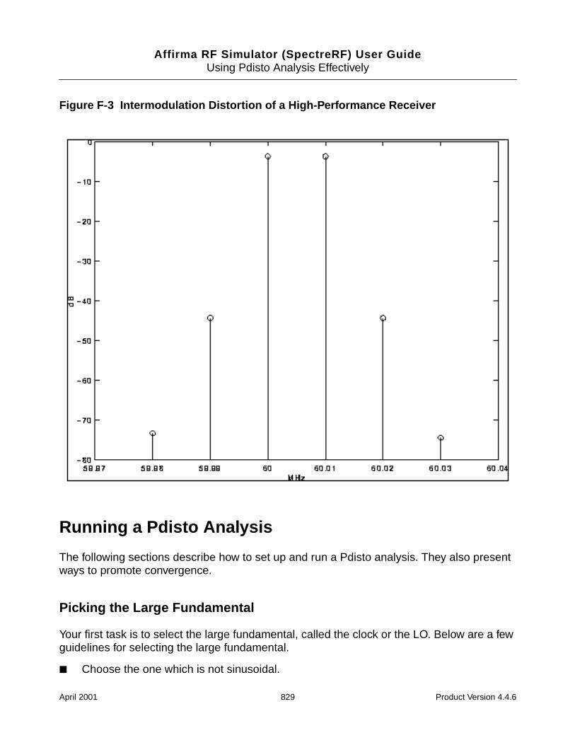
Affirma RF Simulator (SpectreRF) User GuideUsing Pdisto Analysis Effectively
Figure F-3 Intermodulation Distortion of a High-Performance Receiver
Running a Pdisto Analysis
The following sections describe how to set up and run a Pdisto analysis. They also presentways to promote convergence.
Picking the Large Fundamental
Your first task is to select the large fundamental, called the clock or the LO. Below are a fewguidelines for selecting the large fundamental.
Choose the one which is not sinusoidal.
April 2001 829 Product Version 4.4.6
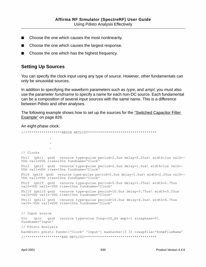
Affirma RF Simulator (SpectreRF) User GuideUsing Pdisto Analysis Effectively
Choose the one which causes the most nonlinearity.
Choose the one which causes the largest response.
Choose the one which has the highest frequency.
Setting Up Sources
You can specify the clock input using any type of source. However, other fundamentals canonly be sinusoidal sources.
In addition to specifying the waveform parameters such as type, and ampl, you must alsouse the parameter fundname to specify a name for each non-DC source. Each fundamentalcan be a composition of several input sources with the same name. This is a differencebetween Pdisto and other analyses.
The following example shows how to set up the sources for the “Switched Capacitor FilterExample” on page 826.
An eight-phase clock:
//******************BEGIN NETLIST**********************************
.
.
.
// Clocks
Phi1 (phi1 gnd) vsource type=pulse period=2.5us delay=0.25us\ width=1us val0=-VDD val1=VDD rise=10ns fundname="Clock"
Phi2 (phi2 gnd) vsource type=pulse period=2.5us delay=1.5us\ width=1us val0=-VDD val1=VDD rise=10ns fundname="Clock"
Phi8 (phi8 gnd) vsource type=pulse period=5.0us delay=1.5us\ width=2.25us val0=-VDD val1=VDD rise=10ns fundname="Clock"
Phi9 (phi9 gnd) vsource type=pulse period=5.0us delay=1.25us\ width=2.75usval0=VDD val1=-VDD rise=10ns fundname="Clock"
Phi10 (phi10 gnd) vsource type=pulse period=10.0us delay=3.75us\ width=5.25usval0=VDD val1=-VDD rise=10ns fundname="Clock"
Phi11 (phi11 gnd) vsource type=pulse period=10.0us delay=4.0us\ width=4.75usval0=-VDD val1=VDD rise=10ns fundname="Clock"
// Input source
Vin (pin gnd) vsource type=sine freq=100_Hz ampl=1 sinephase=0\fundname="Input"
// Pdisto Analysis
harmDisto pdisto funds=["Clock" "Input"] maxharms=[3 3] +swapfile="SomeFileName"
//******************END NETLIST************************************
April 2001 830 Product Version 4.4.6
Affirma RF Simulator (SpectreRF) User GuideUsing Pdisto Analysis Effectively
The following example shows how to set up the sources and analysis for the “High-Performance Receiver Example” on page 827.
//******************BEGIN NETLIST**********************************
.
.
.
// LO input
Vlo (8 7) vsource type=sine ampl=400mV freq=780MegHz fundname="LO"
//RF inputs
Prf1 (15 44) port type=sine ampl=50mV freq=840MegHz fundname="F1"+ ampl2=50mV freq2=840.01MegHz fundname2="F2"
//Analysis
InterModDisto pdisto funds=["LO" "F1" "F2"] maxharms=[5 3 3]+ swapfile="SomeFileName"
//******************END NETLIST***********************************
Sweeping a Pdisto Analysis
You can combine a Pdisto analysis with a Spectre Sweep analysis to create a powerful toolfor a wide variety of applications, such as IP3 and IP5 calculations. For example, you mightwant to calculate the distortion for input power ranging from -60 dBm to 0 dBm. The netlist forthis task is shown below:
//******************BEGIN NETLIST*********************************
.
.
.
parameters inputpower=-60
// Clock
Vlo (clock 0) vsource type=pulse val0=-1 val1=1 period=1n delay=0\ rise=10pfall=10p width=460.00p fundname="carrier"
// Input port
Prf (input 0) port type=sine r=50.0 num=1.0
+freq=+9.0E+08 dbm=inputpower fundname="RF1"
+freq2=+9.05E+08 dbm2=inputpower fundname2="RF2"
// Analysis
swp sweep param=inputpower start=-60 stop=0 lin=6
distortion pdisto funds=["LO" "RF" "RF2"] maxharms=[5 3 3]
April 2001 831 Product Version 4.4.6
Affirma RF Simulator (SpectreRF) User GuideUsing Pdisto Analysis Effectively
//******************END NETLIST***********************************
Always arrange the sweep values so that analyses that converge more easily are performedfirst. When you sweep Pdisto, it automatically uses the converged steady-state solution of theprevious Pdisto analysis as its initial condition and omits the PSS and PAC stage of initialcondition calculations. As discussed in “Convergence Aids” on page 832, this practice canalso aid convergence.
Convergence Aids
Normally Pdisto analysis converges with default parameter settings, but occasionally youmight need to adjust some parameter settings in order to achieve convergence.
There are two situations where non-convergence can occur
During the PSS analysis that Pdisto calls to calculate the initial condition
During the Pdisto iterations
The messages printed on the screen from the simulator identify the problem.
If the simulation fails before printing the message ‘‘Trying PAC for PDISTOinitial condition ’’, the problem is in the PSS analysis.
If it fails after printing ‘‘Starting PDISTO analysis iterations ’’, the problemoccurs during the Pdisto analysis.
Normally, giving a sufficiently large tstab or a looser steadyratio will resolve convergenceproblems during the PSS stage. Also see the convergence aids for PSS analysis inAppendix B, “Running PSS Analysis Effectively”.
For convergence problems during the Pdisto iterations, try the following procedures.
The steadyratio parameter guards against false convergence. Its default values, 1.0 forliberal, 0.1 for moderate, and 0.01 for conservative, are derived from the errpresetparameter. Tighten steadyratio only if you suspect false convergence.
Increase steadyratio. Sometimes steadyratio must be loosened (for example tosteadyratio=1) particularly with a tight reltol setting. Also loosen steadyratio whenconvergence stagnates. An indication of stagnation is that the convNorm value, whichyou can see on the screen, fluctuates within a certain range and never decreases further.
The convergence tolerance of Pdisto is determined by the product of steadyratio andreltol. Normally, you do not set steadyratio to a value higher than 10.
April 2001 832 Product Version 4.4.6
Affirma RF Simulator (SpectreRF) User GuideUsing Pdisto Analysis Effectively
Severe trapezoidal rule ringing can prevent convergence. If you suspect trapezoidal ruleringing, use method=gear2 or method=gear2only.
Avoid using unnecessarily tight reltol settings. Excessively tight reltol significantlyreduces efficiency besides causing convergence problems.
Do a continuation on a parameter, such as input power, of moderate fundamentals.When the circuit is behaving in a highly nonlinear manner at a certain input power level,the PSS plus PAC approach might not compute a good enough estimate of the initialcondition. One effective strategy is to ramp up the input power gradually by carefullyarranging a sweep as described in “Sweeping a Pdisto Analysis” on page 831. Becauseit is usually much easier to achieve convergence at a low power input level where thecircuit behaves in a more linear manner, start with a low input power. Once the simulationconverges, save the steady-state solution as the initial condition for the next input powerlevel. This process repeats automatically as Pdisto is swept. You can achieveconvergence at the desired input power level if the sweep steps are sufficiently small.
In general, avoid using an excessively high number of harmonics for the moderatefundamentals. This practice lengthens the simulation time and uses a lot of memory.However, if the number of harmonics is not high enough for a particular fundamental toadequately model its nonlinear effects, convergence problems might occur.
An important indication of convergence or divergence is the Conv value printed to the screen.There are a few typical scenarios shown in Figure F-4 on page 834.
For most Pdisto runs, the Easy Convergence scenario occurs.
A few simulations follow the Hard Convergence scenario.
If Pdisto iterations Stagnate (Conv value fluctuates close to but above 1.0), loosensteadyratio. Loosening steadyratio will solve the stagnation problem.
If the iterations show Divergence , you usually must improve the initial condition. Do acontinuation on input power level as described within the preceding list.
April 2001 833 Product Version 4.4.6
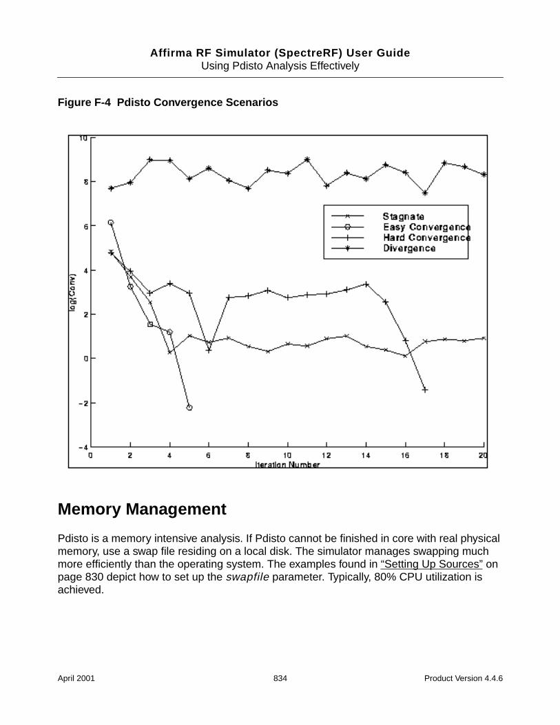
Affirma RF Simulator (SpectreRF) User GuideUsing Pdisto Analysis Effectively
Figure F-4 Pdisto Convergence Scenarios
Memory Management
Pdisto is a memory intensive analysis. If Pdisto cannot be finished in core with real physicalmemory, use a swap file residing on a local disk. The simulator manages swapping muchmore efficiently than the operating system. The examples found in “Setting Up Sources” onpage 830 depict how to set up the swapfile parameter. Typically, 80% CPU utilization isachieved.
April 2001 834 Product Version 4.4.6
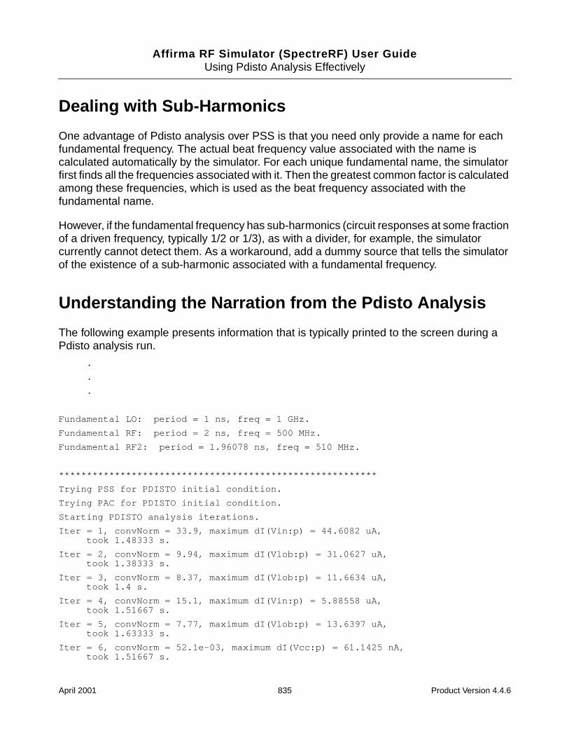
Affirma RF Simulator (SpectreRF) User GuideUsing Pdisto Analysis Effectively
Dealing with Sub-Harmonics
One advantage of Pdisto analysis over PSS is that you need only provide a name for eachfundamental frequency. The actual beat frequency value associated with the name iscalculated automatically by the simulator. For each unique fundamental name, the simulatorfirst finds all the frequencies associated with it. Then the greatest common factor is calculatedamong these frequencies, which is used as the beat frequency associated with thefundamental name.
However, if the fundamental frequency has sub-harmonics (circuit responses at some fractionof a driven frequency, typically 1/2 or 1/3), as with a divider, for example, the simulatorcurrently cannot detect them. As a workaround, add a dummy source that tells the simulatorof the existence of a sub-harmonic associated with a fundamental frequency.
Understanding the Narration from the Pdisto Analysis
The following example presents information that is typically printed to the screen during aPdisto analysis run.
.
.
.
Fundamental LO: period = 1 ns, freq = 1 GHz.
Fundamental RF: period = 2 ns, freq = 500 MHz.
Fundamental RF2: period = 1.96078 ns, freq = 510 MHz.
*********************************************************
Trying PSS for PDISTO initial condition.
Trying PAC for PDISTO initial condition.
Starting PDISTO analysis iterations.
Iter = 1, convNorm = 33.9, maximum dI(Vin:p) = 44.6082 uA,took 1.48333 s.
Iter = 2, convNorm = 9.94, maximum dI(Vlob:p) = 31.0627 uA,took 1.38333 s.
Iter = 3, convNorm = 8.37, maximum dI(Vlob:p) = 11.6634 uA,took 1.4 s.
Iter = 4, convNorm = 15.1, maximum dI(Vin:p) = 5.88558 uA,took 1.51667 s.
Iter = 5, convNorm = 7.77, maximum dI(Vlob:p) = 13.6397 uA,took 1.63333 s.
Iter = 6, convNorm = 52.1e-03, maximum dI(Vcc:p) = 61.1425 nA,took 1.51667 s.
April 2001 835 Product Version 4.4.6
Affirma RF Simulator (SpectreRF) User GuideUsing Pdisto Analysis Effectively
PDISTO solution has converged. Starting spectrum calculation.
.
.
.
The simulator first confirms the fundamental names that have been read and their beatfrequencies. For the preceding example, the circuit has a 1 GHz fundamental named LO asthe clock, and two fundamentals named RF and RF2, respectively, as inputs. Theirassociated frequencies are 500 MHz and 510 MHz, respectively.
Before starting the PSS analysis to determine initial condition calculations, the followingmessages is printed.
Trying PSS for PDisto initial condition.
After the PSS is finished, the following message is printed. This tells you that a PAC analysisis started to perform further initial condition calculations.
Trying PAC for PDISTO initial condition.
Once the initial condition is obtained, Pdisto prints the following and begins Pdisto nonlineariterations.
Starting PDISTO analysis iterations.
At the end of each iteration, a few pieces of information such as the iteration number, itsconvergence norm, which node had the maximum deviation, and the amount of CPU timespent in the iteration, are printed.
Occasionally, you might see warning messages such as the following
Minimum time step used. Solution might be in error.
or
Junction current exceeds ‘imelt’. The results computed by Spectre are now incorrectbecause the junction current model has been linearized.
You can ignore these warning messages if they appear in the early stage of Pdisto iterationsor in the initial condition calculations (PSS). They might be caused by bad starting integrationconditions and do not affect the final solution. However, if they appear in the final iteration, thesolution might be in error.
References
[1] A. ALLGOWER AND K. GEORG, Numerical Continuation Methods,Springer-Verlag, New York, 1990.
April 2001 836 Product Version 4.4.6
Affirma RF Simulator (SpectreRF) User GuideUsing Pdisto Analysis Effectively
[2] L. O. CHUA AND A. USHIDA, Algorithms for computing almost periodicsteady-state response of nonlinear systems to multiple inputfrequencies, IEEE Trans. Circuits and Systems, 28 (1981), pp. 953-971.
[3] D. FENG, J. PHILLIPS, K. NABORS, K. KUNDERT, AND J. WHITE, Efficientcomputation of quasi-periodic circuit operating conditions via a mixedfrequency/time approach. Submitted to Proceedings of the 36th DesignAutomation Conference, June 1999.
[4] K. KUNDERT, J. WHITE, AND A. SANGIOVANNI-VINCENTELLI, A mixedfrequency-time approach for distortion analysis of switching filtercircuits, IEEE J. Solid State Circuits, 24 (1989), pp. 443-451.
[5] P. LANCASTER AND M. TISMENETSKY, The Theory of Matrices,Academic Press, second ed., 1985.
[6] Y. SAAD, Iterative methods for sparse linear systems, PWS PublishingCompany, 1996.
[7] R. TELICHEVESKY, K. S. KUNDERT, AND J. K. WHITE, Efficientsteady-state analysis based on matrix-free Krylov-subspacemethods, in Proceedings of the 1995 Design Automation Conference, June1995.
[8] _____, Efficient AC and noise analysis of two-tone RF circuits, inProceedings of the 1996 Design Automation Conference, June 1996.
April 2001 837 Product Version 4.4.6
Affirma RF Simulator (SpectreRF) User Guide
GAn Introduction to the PLL library
The models in the new phaselock loop (PLL) library support top-down design of PLLs. Figure1 shows the three steps of the design flow. This paper describes the first step in detail, but allthree steps are described briefly.
The first step in Figure 1 is to develop an executable specification. The executablespecification is an arrangement of fast behavioral models. The executable specificationpermits fast architectural studies and separates specification and implementation issues. Theexecutable specification contains baseband models [11,2,3,4,5,6,7,8,9]. These basebandmodels suppress clocks and RF/IF carriers. Some literature refers to PLL baseband modelsas “relative phase” or “phase-domain” models [2]. This paper uses the latter term. Phase-domain PLL models are exceptionally fast, capture the important non-linear mechanisms,and can be linearized directly for AC analysis.
1. This reference uses the terms “baseband” and “bandpass” explicitly.
April 2001 838 Product Version 4.4.6
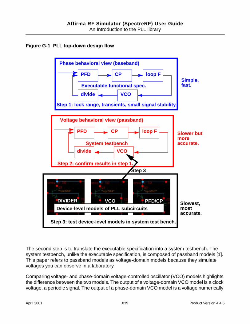
Affirma RF Simulator (SpectreRF) User GuideAn Introduction to the PLL library
Figure G-1 PLL top-down design flow
The second step is to translate the executable specification into a system testbench. Thesystem testbench, unlike the executable specification, is composed of passband models [1].This paper refers to passband models as voltage-domain models because they simulatevoltages you can observe in a laboratory.
Comparing voltage- and phase-domain voltage-controlled oscillator (VCO) models highlightsthe difference between the two models. The output of a voltage-domain VCO model is a clockvoltage, a periodic signal. The output of a phase-domain VCO model is a voltage numerically
VCO
PFD CP
divide
loop F
VCO
PFD CP
divide
loop F
Phase behavioral view (baseband)
Voltage behavioral view (passband)
VCO PFD/CPDIVIDER
Device-level models of PLL subcircuits
Step 1: lock range, transients, small signal stability
Step 2: confirm results in step 1.
Step 3: test device-level models in system test bench.
Step 3
Executable functional spec.
System testbench
Simple,
Slower but
Slowest,
fast.
moreaccurate.
mostaccurate.
April 2001 839 Product Version 4.4.6
Affirma RF Simulator (SpectreRF) User GuideAn Introduction to the PLL library
equal to phase. If you unwrap the VCO phase, in steady state, it ramps up indefinitely.Unwrapped phase is not periodic. Voltage-domain models describe non-linear effects relatedto the shapes of the actual RF waveforms. Such waveform effects include spurs andharmonic locking1. Phase-domain models do not simulate waveform effects. The systemtestbench is more accurate than the executable specification, but it is still behavioral.Equipped only with behavioral voltage-domain models, the testbench does not simulatedevice-level effects associated with specific implementations. Examples of suchimplementation effects are interstage loading, improper bias, and device parasitics.
The last step in Figure 1 is to gradually replace the behavioral models in the system testbenchwith device-level models, one or two blocks at a time. Device-level models check for thepreviously mentioned implementation problems. The entire PLL is simulated at the device-level only as a final verification step because such simulations are very lengthy.
The Models in the PLL library
The new PLL library includes the following phase-domain models:
Analog multiplier phase detector
XOR phase detector with bipolar output2
Three-state digital phase frequency detector (PFD)
Charge pump (current source version)
VCO tuning curve (analytic and tabular versions)
Frequency divider
Lock indicator
Introduction
The primary system-level specifications captured by this first set of phase-domain models areacquisition time, lock and capture ranges [12], and phase margin. The PFD model alsosimulates backlash3 [8].
1. “Harmonic locking” is when the PLL locks on to a harmonic of the reference.
2. The XOR phase detector is not explicitly discussed in this application note because it is very similar to theanalog multiplier phase detector. The only difference is that the duty cycle-phase error transfer curve istriangular instead of sinusoidal.
3. Backlash is sometimes called “deadband” effect. It is a limit cycle caused by the phase-frequency detec-tor’s inability to linearly reduce its output pulse width to zero as phase error goes to zero.
April 2001 840 Product Version 4.4.6
Affirma RF Simulator (SpectreRF) User GuideAn Introduction to the PLL library
The remainder of this paper is divided into two main sections. The first section introducesphase-domain modeling, describes a feature included to prevent DC convergence problems,and then shows you some examples of using phase- domain models. The second sectionexplains how to assemble a more complex PLL and discusses an example. The examples areintroductory and are not a comprehensive discussion of all applications of phase-domainmodels.
Phase-Domain Model of a Simple PLL
Description
This PLL example, which is built around the simplest phase detector in the new library,introduces the fundamentals of phase-domain modeling. Figure 2 shows a voltage-domainmodel of the example and also some selected waveforms.The phase detector in this case isan ideal analog multiplier. Figure 3 shows the equivalent phase-domain model. The phase-domain model is based on the trigonometric identity below:
sin(θ1)*cos(θ2) = (1/2)*[sin(θ1+θ2)+sin(θ1−θ2)], which after filtering is approximately
(1/2)*sin(θ1−θ2).
Note: θ1+θ2 = (ω1+ω2)*t, and ω1+ω2 usually lies far beyond the filter corner frequency.
April 2001 841 Product Version 4.4.6
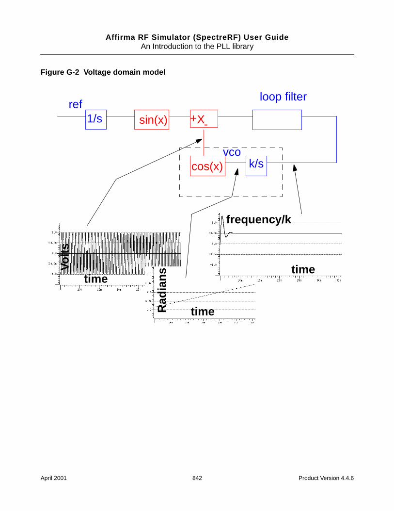
Affirma RF Simulator (SpectreRF) User GuideAn Introduction to the PLL library
Figure G-2 Voltage domain model
1/s
k/s
sin(x)
cos(x)
+ -
loop filterref
vco
X
Figure 1, classical non-linear model
Volts
time
timeRad
ians
time
frequency/k
April 2001 842 Product Version 4.4.6
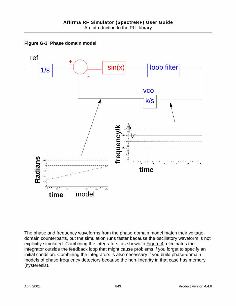
Affirma RF Simulator (SpectreRF) User GuideAn Introduction to the PLL library
Figure G-3 Phase domain model
The phase and frequency waveforms from the phase-domain model match their voltage-domain counterparts, but the simulation runs faster because the oscillatory waveform is notexplicitly simulated. Combining the integrators, as shown in Figure 4, eliminates theintegrator outside the feedback loop that might cause problems if you forget to specify aninitial condition. Combining the integrators is also necessary if you build phase-domainmodels of phase-frequency detectors because the non-linearity in that case has memory(hysteresis).
1/s
k/s
sin(x) loop filterref
vco
+
-
modeltime
Rad
ians
time
freq
uenc
y/k
April 2001 843 Product Version 4.4.6
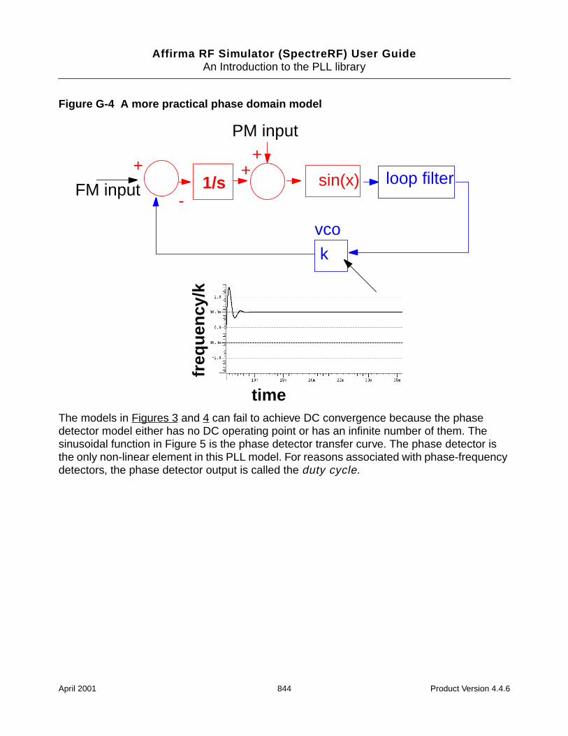
Affirma RF Simulator (SpectreRF) User GuideAn Introduction to the PLL library
Figure G-4 A more practical phase domain model
The models in Figures 3 and 4 can fail to achieve DC convergence because the phasedetector model either has no DC operating point or has an infinite number of them. Thesinusoidal function in Figure 5 is the phase detector transfer curve. The phase detector isthe only non-linear element in this PLL model. For reasons associated with phase-frequencydetectors, the phase detector output is called the duty cycle.
k
sin(x) loop filterFM input
vco
+
-
time
freq
uenc
y/k
1/s
PM input+
+
April 2001 844 Product Version 4.4.6
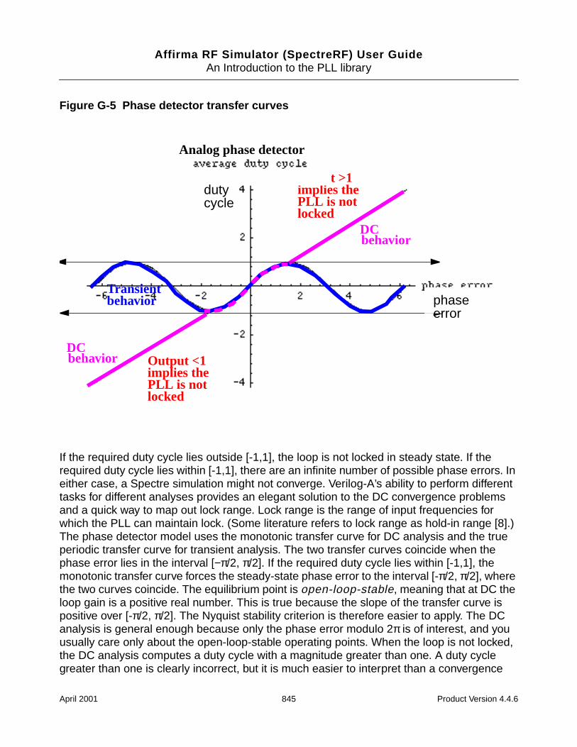
Affirma RF Simulator (SpectreRF) User GuideAn Introduction to the PLL library
Figure G-5 Phase detector transfer curves
If the required duty cycle lies outside [-1,1], the loop is not locked in steady state. If therequired duty cycle lies within [-1,1], there are an infinite number of possible phase errors. Ineither case, a Spectre simulation might not converge. Verilog-A’s ability to perform differenttasks for different analyses provides an elegant solution to the DC convergence problemsand a quick way to map out lock range. Lock range is the range of input frequencies forwhich the PLL can maintain lock. (Some literature refers to lock range as hold-in range [8].)The phase detector model uses the monotonic transfer curve for DC analysis and the trueperiodic transfer curve for transient analysis. The two transfer curves coincide when thephase error lies in the interval [−π/2, π/2]. If the required duty cycle lies within [-1,1], themonotonic transfer curve forces the steady-state phase error to the interval [-π/2, π/2], wherethe two curves coincide. The equilibrium point is open-loop-stable, meaning that at DC theloop gain is a positive real number. This is true because the slope of the transfer curve ispositive over [-π/2, π/2]. The Nyquist stability criterion is therefore easier to apply. The DCanalysis is general enough because only the phase error modulo 2π is of interest, and youusually care only about the open-loop-stable operating points. When the loop is not locked,the DC analysis computes a duty cycle with a magnitude greater than one. A duty cyclegreater than one is clearly incorrect, but it is much easier to interpret than a convergence
Analog phase detector
DCbehavior
output >1implies thePLL is notlocked
Output <1implies thePLL is notlocked
DCbehavior
Transientbehavior
dutycycle
phaseerror
April 2001 845 Product Version 4.4.6
Affirma RF Simulator (SpectreRF) User GuideAn Introduction to the PLL library
error. DC duty cycle is a lock indicator which can be used in a parametric DC analysis tosweep out lock range.
Example 1: A dynamic test for capture range and lock range (example_analog_PD inpllLib).
Capture range is the range of input frequencies that the PLL can acquire from an unlockedstate. Since acquisition of frequencies near the edge of the capture range involves a pull-inmechanism [1-12], measuring the capture range requires a transient analysis. You canmeasure capture and lock ranges by slowly sweeping the input frequency and observing thefrequency at which the duty cycle begins and ends a long ramp [12]. You must skip the DCanalysis to observe the capture limits. Figure 6 plots the VCO control voltage against theinput frequency voltage. The input frequency first ramps up and then down. A bufferedauxiliary circuit responds to the duty cycle and adds 2.5 volts when the input frequencychanges direction. This technique makes the plot easier to read because the forward andreverse sweeps occupy different parts of the vertical scale. In this example, lock range isfrom 1.36Khz to 3.4Khz, and the capture range is from 1.8Khz to 3Khz.
Figure 7 compares VCO control voltages in the forward sweep when computed with voltage-or phase-domain models. The models produce similar results. In this example (2.5Khzcenter frequency), the phase-domain model is only about 20 times faster than the voltage-domain model.
April 2001 846 Product Version 4.4.6
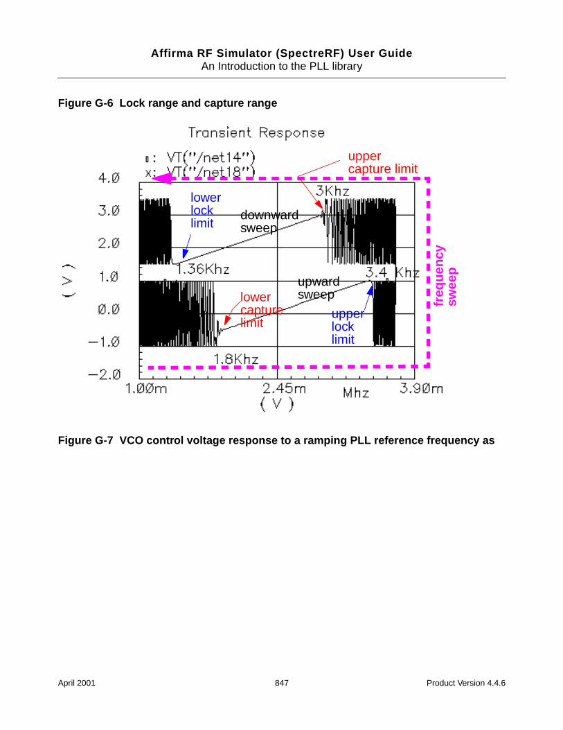
Affirma RF Simulator (SpectreRF) User GuideAn Introduction to the PLL library
Figure G-6 Lock range and capture range
Figure G-7 VCO control voltage response to a ramping PLL reference frequency as
lowerlocklimit
uppercapture limit
upperlocklimit
lowercapturelimit
freq
uenc
ysw
eep
upwardsweep
downwardsweep
April 2001 847 Product Version 4.4.6
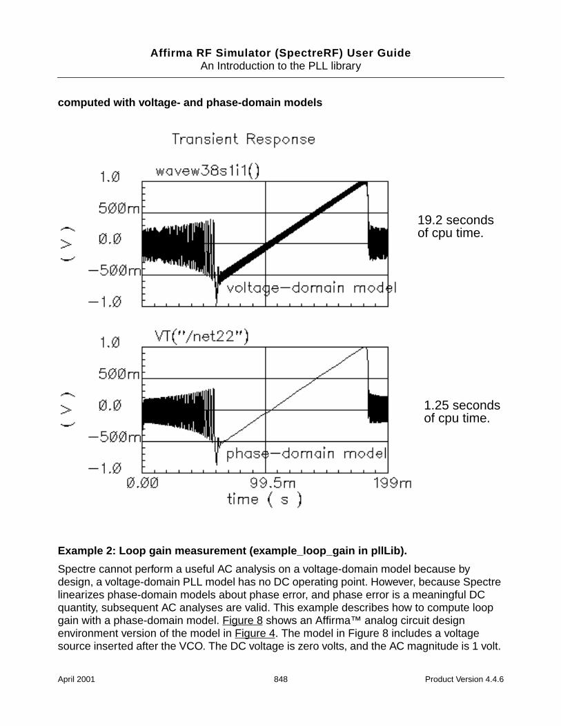
Affirma RF Simulator (SpectreRF) User GuideAn Introduction to the PLL library
computed with voltage- and phase-domain models
Example 2: Loop gain measurement (example_loop_gain in pllLib).
Spectre cannot perform a useful AC analysis on a voltage-domain model because bydesign, a voltage-domain PLL model has no DC operating point. However, because Spectrelinearizes phase-domain models about phase error, and phase error is a meaningful DCquantity, subsequent AC analyses are valid. This example describes how to compute loopgain with a phase-domain model. Figure 8 shows an Affirma™ analog circuit designenvironment version of the model in Figure 4. The model in Figure 8 includes a voltagesource inserted after the VCO. The DC voltage is zero volts, and the AC magnitude is 1 volt.
19.2 seconds
1.25 seconds
of cpu time.
of cpu time.
April 2001 848 Product Version 4.4.6
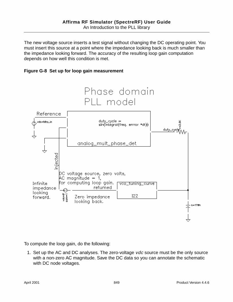
Affirma RF Simulator (SpectreRF) User GuideAn Introduction to the PLL library
The new voltage source inserts a test signal without changing the DC operating point. Youmust insert this source at a point where the impedance looking back is much smaller thanthe impedance looking forward. The accuracy of the resulting loop gain computationdepends on how well this condition is met.
Figure G-8 Set up for loop gain measurement
To compute the loop gain, do the following:
1. Set up the AC and DC analyses. The zero-voltage vdc source must be the only sourcewith a non-zero AC magnitude. Save the DC data so you can annotate the schematicwith DC node voltages.
April 2001 849 Product Version 4.4.6
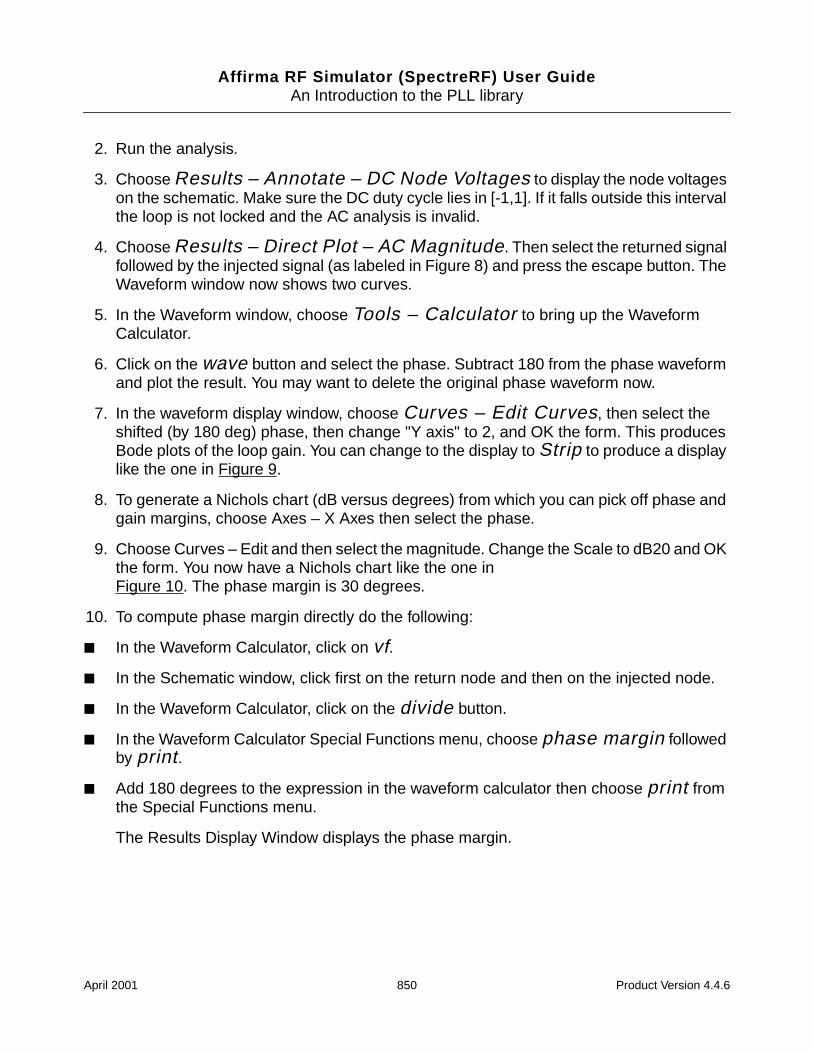
Affirma RF Simulator (SpectreRF) User GuideAn Introduction to the PLL library
2. Run the analysis.
3. Choose Results – Annotate – DC Node Voltages to display the node voltageson the schematic. Make sure the DC duty cycle lies in [-1,1]. If it falls outside this intervalthe loop is not locked and the AC analysis is invalid.
4. Choose Results – Direct Plot – AC Magnitude. Then select the returned signalfollowed by the injected signal (as labeled in Figure 8) and press the escape button. TheWaveform window now shows two curves.
5. In the Waveform window, choose Tools – Calculator to bring up the WaveformCalculator.
6. Click on the wave button and select the phase. Subtract 180 from the phase waveformand plot the result. You may want to delete the original phase waveform now.
7. In the waveform display window, choose Curves – Edit Curves, then select theshifted (by 180 deg) phase, then change "Y axis" to 2, and OK the form. This producesBode plots of the loop gain. You can change to the display to Strip to produce a displaylike the one in Figure 9.
8. To generate a Nichols chart (dB versus degrees) from which you can pick off phase andgain margins, choose Axes – X Axes then select the phase.
9. Choose Curves – Edit and then select the magnitude. Change the Scale to dB20 and OKthe form. You now have a Nichols chart like the one inFigure 10. The phase margin is 30 degrees.
10. To compute phase margin directly do the following:
In the Waveform Calculator, click on vf.
In the Schematic window, click first on the return node and then on the injected node.
In the Waveform Calculator, click on the divide button.
In the Waveform Calculator Special Functions menu, choose phase margin followedby print.
Add 180 degrees to the expression in the waveform calculator then choose print fromthe Special Functions menu.
The Results Display Window displays the phase margin.
April 2001 850 Product Version 4.4.6
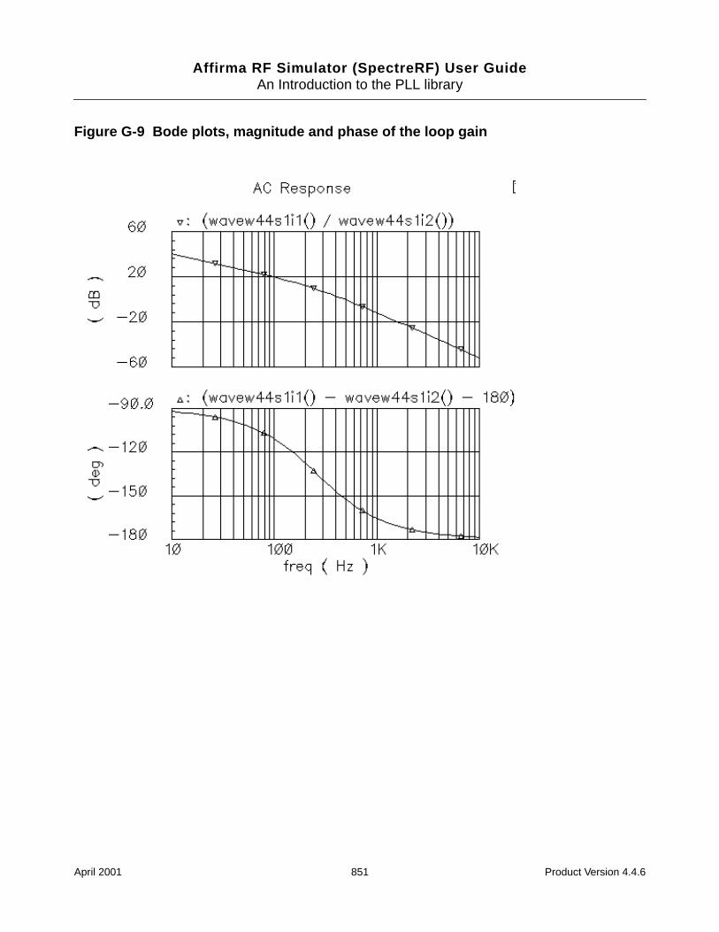
Affirma RF Simulator (SpectreRF) User GuideAn Introduction to the PLL library
Figure G-9 Bode plots, magnitude and phase of the loop gain
April 2001 851 Product Version 4.4.6
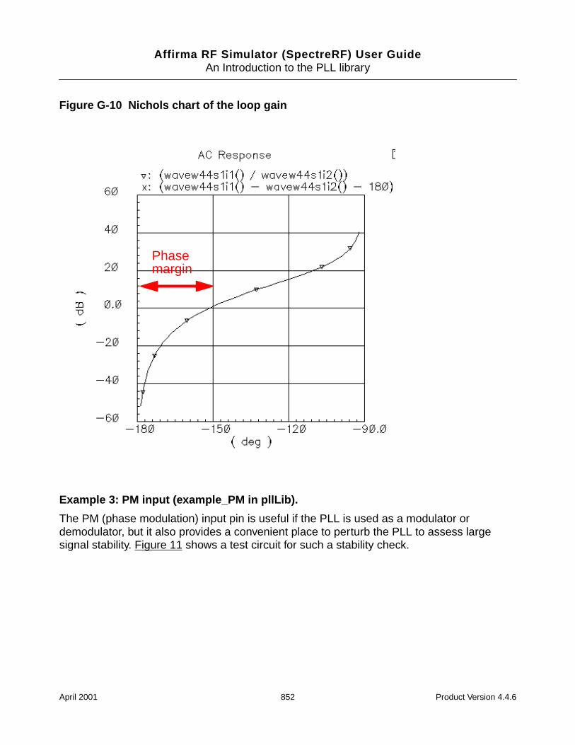
Affirma RF Simulator (SpectreRF) User GuideAn Introduction to the PLL library
Figure G-10 Nichols chart of the loop gain
Example 3: PM input (example_PM in pllLib).
The PM (phase modulation) input pin is useful if the PLL is used as a modulator ordemodulator, but it also provides a convenient place to perturb the PLL to assess largesignal stability. Figure 11 shows a test circuit for such a stability check.
Phasemargin
April 2001 852 Product Version 4.4.6
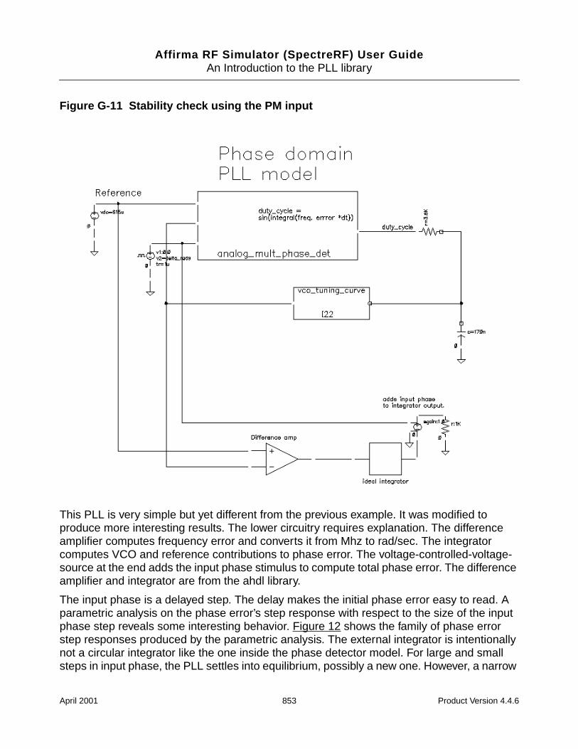
Affirma RF Simulator (SpectreRF) User GuideAn Introduction to the PLL library
Figure G-11 Stability check using the PM input
This PLL is very simple but yet different from the previous example. It was modified toproduce more interesting results. The lower circuitry requires explanation. The differenceamplifier computes frequency error and converts it from Mhz to rad/sec. The integratorcomputes VCO and reference contributions to phase error. The voltage-controlled-voltage-source at the end adds the input phase stimulus to compute total phase error. The differenceamplifier and integrator are from the ahdl library.
The input phase is a delayed step. The delay makes the initial phase error easy to read. Aparametric analysis on the phase error’s step response with respect to the size of the inputphase step reveals some interesting behavior. Figure 12 shows the family of phase errorstep responses produced by the parametric analysis. The external integrator is intentionallynot a circular integrator like the one inside the phase detector model. For large and smallsteps in input phase, the PLL settles into equilibrium, possibly a new one. However, a narrow
April 2001 853 Product Version 4.4.6
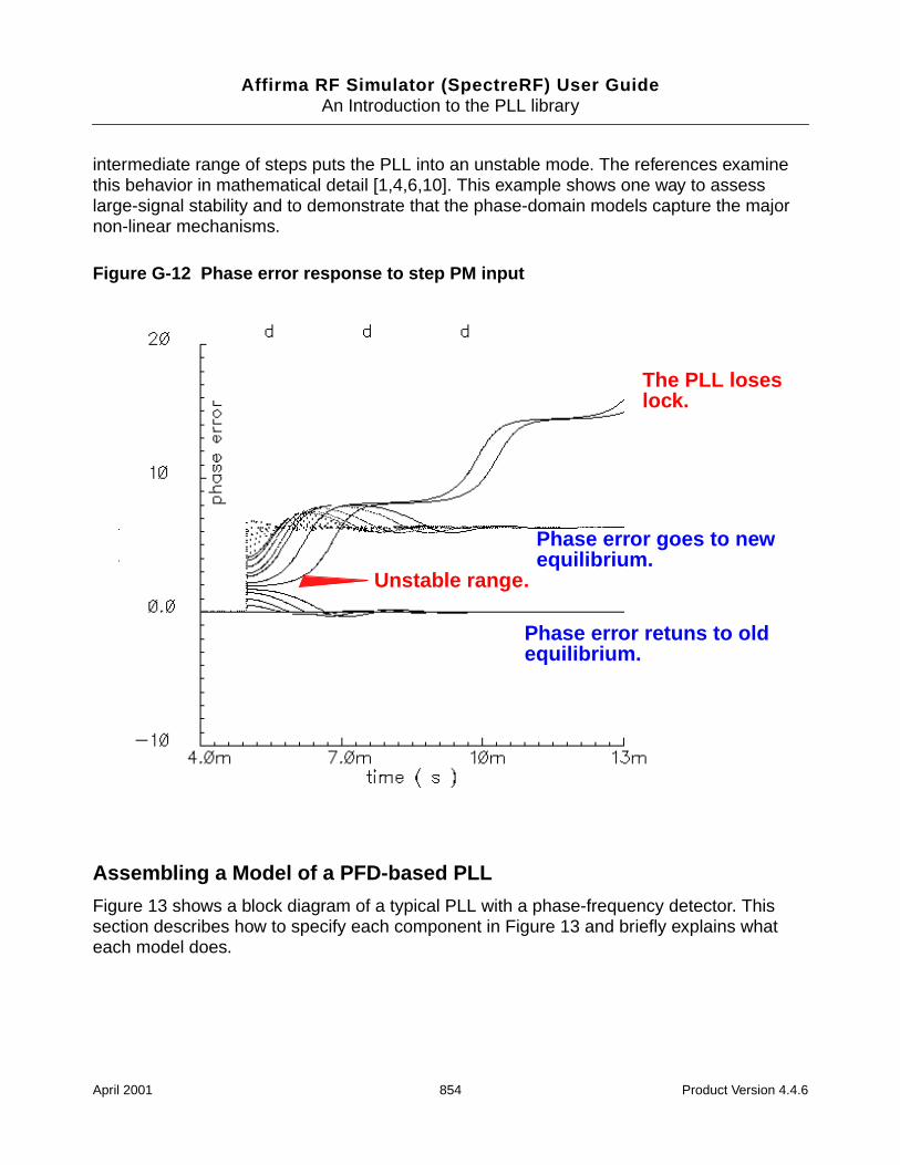
Affirma RF Simulator (SpectreRF) User GuideAn Introduction to the PLL library
intermediate range of steps puts the PLL into an unstable mode. The references examinethis behavior in mathematical detail [1,4,6,10]. This example shows one way to assesslarge-signal stability and to demonstrate that the phase-domain models capture the majornon-linear mechanisms.
Figure G-12 Phase error response to step PM input
Assembling a Model of a PFD-based PLL
Figure 13 shows a block diagram of a typical PLL with a phase-frequency detector. Thissection describes how to specify each component in Figure 13 and briefly explains whateach model does.
Phase error retuns to oldequilibrium.
Phase error goes to newequilibrium.
The PLL loseslock.
Unstable range.
April 2001 854 Product Version 4.4.6
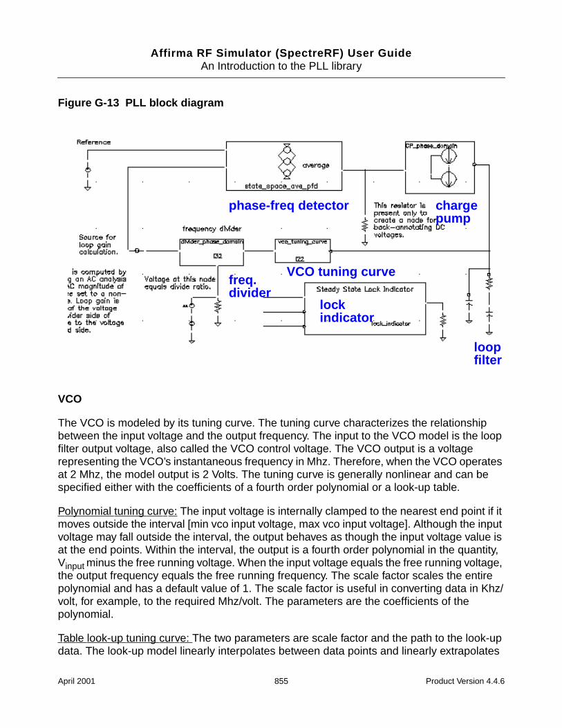
Affirma RF Simulator (SpectreRF) User GuideAn Introduction to the PLL library
Figure G-13 PLL block diagram
VCO
The VCO is modeled by its tuning curve. The tuning curve characterizes the relationshipbetween the input voltage and the output frequency. The input to the VCO model is the loopfilter output voltage, also called the VCO control voltage. The VCO output is a voltagerepresenting the VCO’s instantaneous frequency in Mhz. Therefore, when the VCO operatesat 2 Mhz, the model output is 2 Volts. The tuning curve is generally nonlinear and can bespecified either with the coefficients of a fourth order polynomial or a look-up table.
Polynomial tuning curve: The input voltage is internally clamped to the nearest end point if itmoves outside the interval [min vco input voltage, max vco input voltage]. Although the inputvoltage may fall outside the interval, the output behaves as though the input voltage value isat the end points. Within the interval, the output is a fourth order polynomial in the quantity,Vinput minus the free running voltage. When the input voltage equals the free running voltage,the output frequency equals the free running frequency. The scale factor scales the entirepolynomial and has a default value of 1. The scale factor is useful in converting data in Khz/volt, for example, to the required Mhz/volt. The parameters are the coefficients of thepolynomial.
Table look-up tuning curve: The two parameters are scale factor and the path to the look-updata. The look-up model linearly interpolates between data points and linearly extrapolates
phase-freq detector chargepump
freq.divider
VCO tuning curve
lockindicator
loopfilter
April 2001 855 Product Version 4.4.6
Affirma RF Simulator (SpectreRF) User GuideAn Introduction to the PLL library
outside the data interval. The data format is two columns of data delimited by spaces. Thereis no header, and there are no extra lines at the end. The first column is input voltage. Thesecond column is output frequency. The path to the data can be absolute or relative to thenetlist. The netlist is usually stored at
<home>/simulation/ckt_name/spectre/schematic/netlist/input.scs
but you can choose a different location.
If the data is at <home>/data/table and the netlist is as shown above, the relative path is
../../../../../data/table.
Frequency Divider
The frequency divider is essentially a simple gain element. It takes an input voltage thatrepresents frequency in Mhz, and then scales it by the divide ratio to generate an outputvoltage that represents the divided frequency. The divide ratio is numerically equal to thevoltage on the control pin. If the divide ratio drops below 0.001, the model assigns it to 0.001and issues a warning. This assignment prevents division by zero during simulation.
Charge Pump
The charge pump transforms the duty cycle into the expected average current sourced orsunk by the charge pump. You define the maximum source and sink currents, and they canbe different from each other. If the charge pump output voltage exceeds the rails you define,the output voltage is clamped to the rail through a 0.001 Ohm resistance. The otherparameters are the leakage resistance and open circuit voltage. These last two parametersspecify the Thevenin equivalent circuit of a leakage path. The leakage path can source or sinkcurrent depending on the open circuit voltage.
Loop Filter
The loop filter is entered component-for-component.
State-space averaged PFD (Phase-domain phase-frequency detector model.
The phase-frequency detector (PFD) model approximates average behavior of a digital,three-state, phase frequency detector. This is the most complicated model in the PLL library.The term state-space averaged is borrowed from the power electronics field [14]. Thecharge pump currents for the three PFD states are averaged together with a duty cycle much
April 2001 856 Product Version 4.4.6
Affirma RF Simulator (SpectreRF) User GuideAn Introduction to the PLL library
like voltages are averaged together with a duty cycle in a switch-mode power supply model.The PFD inputs are voltages representing the reference and divider output frequencies inMhz. The output is a voltage that when multiplied by the maximum charge pump current,numerically equals the average charge-pump output current. The PFD output is a duty cycle.When the frequency error is large, the duty cycle is a smooth waveform directly related to thenormalized frequency error [1,4]. When the frequency error is small, an integrator inside thePFD model converts frequency error to phase error, and the duty cycle is proportional to thephase error. The duty cycle starts jumping to zero (or resets) as it changes from frequency-mode to phase-mode.
As phase error enters a deadband determined by the minimum-on-time parameter andreference frequency, the model computes a duty cycle pulse with magnitude one and durationequal to the minimum-pulse-width. After the pulse expires, the duty cycle drops to zero untilthe phase error exits the deadband. As the phase error exits the deadband, the duty cycleincreases to a non-zero value. The deadband and fixed-width unity pulse simulate what sometexts call backlash [8].
The PFD model has two parameters. The first is a numerical option that controls the trade-offbetween execution speed and accuracy. The speed_vs_accuracy parameter controls thenumber of times the internal integrator is reset during the transition from frequency-mode tophase-mode. Too few resets can cause error. Too many resets can needlessly slow run time.The default value of this parameter is 50k. To reduce the number of resets in a slow PLL, andthereby reduce run time, increase the speed_vs_accuracy parameter to 70k or 100k. Toincrease the number of resets in fast PLLs, and thereby increase the accuracy, reduce thespeed_vs_accuracy parameter to 10k or 20k. A reasonable setting for thespeed_vs_accuracy parameter produces a duty cycle step response that resetsapproximately to zero at least 3-10 times before entering the final transient. Figure 14 showsreasonable duty cycle step response.
April 2001 857 Product Version 4.4.6
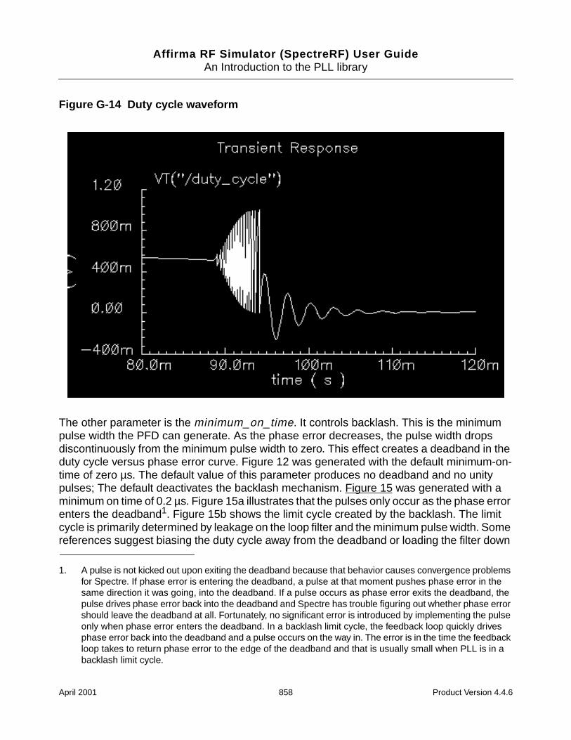
Affirma RF Simulator (SpectreRF) User GuideAn Introduction to the PLL library
Figure G-14 Duty cycle waveform
The other parameter is the minimum_on_time. It controls backlash. This is the minimumpulse width the PFD can generate. As the phase error decreases, the pulse width dropsdiscontinuously from the minimum pulse width to zero. This effect creates a deadband in theduty cycle versus phase error curve. Figure 12 was generated with the default minimum-on-time of zero µs. The default value of this parameter produces no deadband and no unitypulses; The default deactivates the backlash mechanism. Figure 15 was generated with aminimum on time of 0.2 µs. Figure 15a illustrates that the pulses only occur as the phase errorenters the deadband1. Figure 15b shows the limit cycle created by the backlash. The limitcycle is primarily determined by leakage on the loop filter and the minimum pulse width. Somereferences suggest biasing the duty cycle away from the deadband or loading the filter down
1. A pulse is not kicked out upon exiting the deadband because that behavior causes convergence problemsfor Spectre. If phase error is entering the deadband, a pulse at that moment pushes phase error in thesame direction it was going, into the deadband. If a pulse occurs as phase error exits the deadband, thepulse drives phase error back into the deadband and Spectre has trouble figuring out whether phase errorshould leave the deadband at all. Fortunately, no significant error is introduced by implementing the pulseonly when phase error enters the deadband. In a backlash limit cycle, the feedback loop quickly drivesphase error back into the deadband and a pulse occurs on the way in. The error is in the time the feedbackloop takes to return phase error to the edge of the deadband and that is usually small when PLL is in abacklash limit cycle.
April 2001 858 Product Version 4.4.6
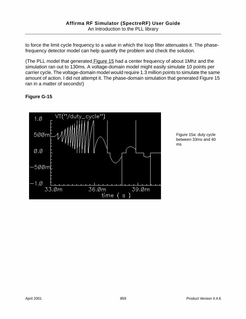
Affirma RF Simulator (SpectreRF) User GuideAn Introduction to the PLL library
to force the limit cycle frequency to a value in which the loop filter attenuates it. The phase-frequency detector model can help quantify the problem and check the solution.
(The PLL model that generated Figure 15 had a center frequency of about 1Mhz and thesimulation ran out to 130ms. A voltage-domain model might easily simulate 10 points percarrier cycle. The voltage-domain model would require 1.3 million points to simulate the sameamount of action. I did not attempt it. The phase-domain simulation that generated Figure 15ran in a matter of seconds!)
Figure G-15
Figure 15a: duty cyclebetween 33ms and 40ms
April 2001 859 Product Version 4.4.6
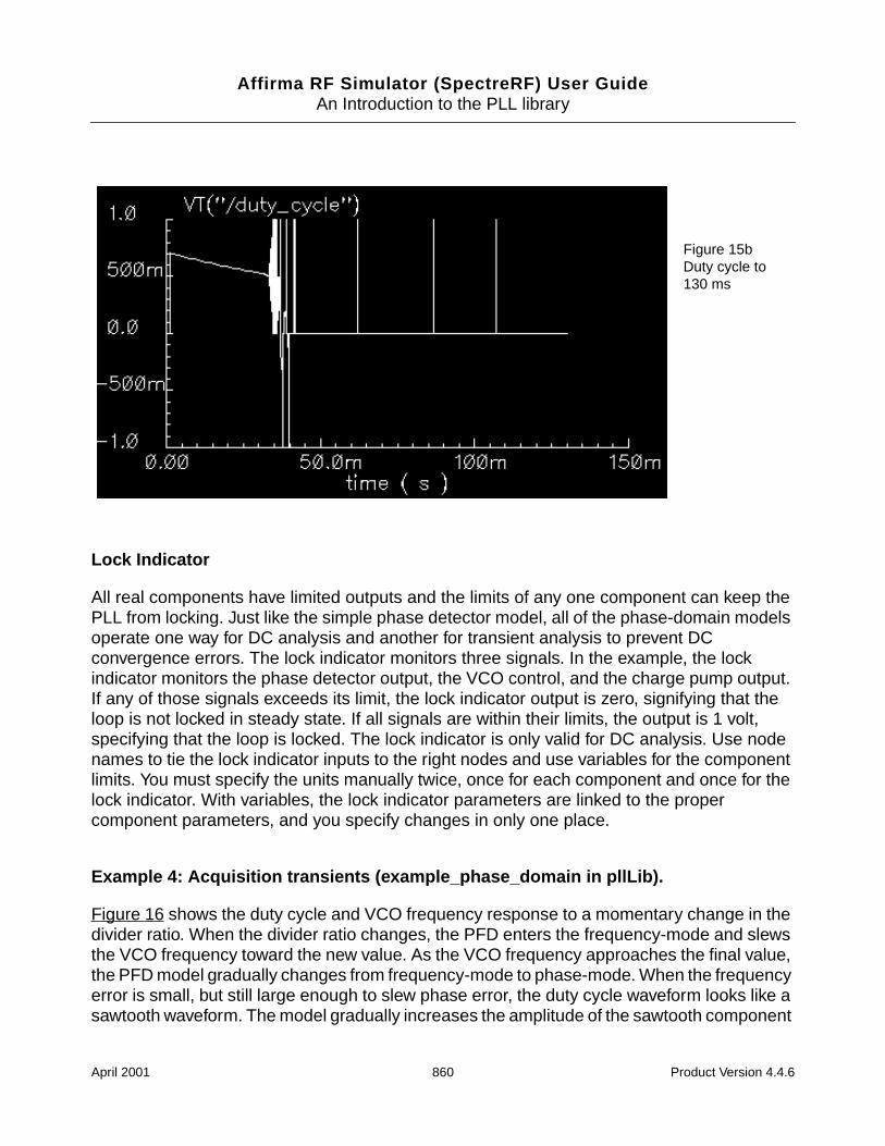
Affirma RF Simulator (SpectreRF) User GuideAn Introduction to the PLL library
Lock Indicator
All real components have limited outputs and the limits of any one component can keep thePLL from locking. Just like the simple phase detector model, all of the phase-domain modelsoperate one way for DC analysis and another for transient analysis to prevent DCconvergence errors. The lock indicator monitors three signals. In the example, the lockindicator monitors the phase detector output, the VCO control, and the charge pump output.If any of those signals exceeds its limit, the lock indicator output is zero, signifying that theloop is not locked in steady state. If all signals are within their limits, the output is 1 volt,specifying that the loop is locked. The lock indicator is only valid for DC analysis. Use nodenames to tie the lock indicator inputs to the right nodes and use variables for the componentlimits. You must specify the units manually twice, once for each component and once for thelock indicator. With variables, the lock indicator parameters are linked to the propercomponent parameters, and you specify changes in only one place.
Example 4: Acquisition transients (example_phase_domain in pllLib).
Figure 16 shows the duty cycle and VCO frequency response to a momentary change in thedivider ratio. When the divider ratio changes, the PFD enters the frequency-mode and slewsthe VCO frequency toward the new value. As the VCO frequency approaches the final value,the PFD model gradually changes from frequency-mode to phase-mode. When the frequencyerror is small, but still large enough to slew phase error, the duty cycle waveform looks like asawtooth waveform. The model gradually increases the amplitude of the sawtooth component
Figure 15bDuty cycle to130 ms
April 2001 860 Product Version 4.4.6
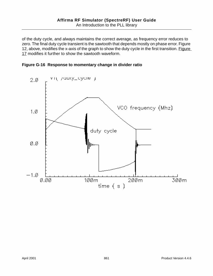
Affirma RF Simulator (SpectreRF) User GuideAn Introduction to the PLL library
of the duty cycle, and always maintains the correct average, as frequency error reduces tozero. The final duty cycle transient is the sawtooth that depends mostly on phase error. Figure12, above, modifies the x-axis of the graph to show the duty cycle in the first transition. Figure17 modifies it further to show the sawtooth waveform.
Figure G-16 Response to momentary change in divider ratio
April 2001 861 Product Version 4.4.6
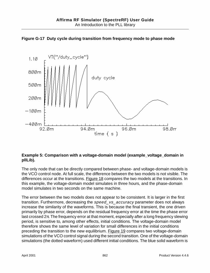
Affirma RF Simulator (SpectreRF) User GuideAn Introduction to the PLL library
Figure G-17 Duty cycle during transition from frequency mode to phase mode
Example 5: Comparison with a voltage-domain model (example_voltage_domain inpllLib).
The only node that can be directly compared between phase- and voltage-domain models isthe VCO control node. At full scale, the difference between the two models is not visible. Thedifferences occur at the transitions. Figure 18 compares the two models at the transitions. Inthis example, the voltage-domain model simulates in three hours, and the phase-domainmodel simulates in two seconds on the same machine.
The error between the two models does not appear to be consistent. It is larger in the firsttransition. Furthermore, decreasing the speed_vs_accuracy parameter does not alwaysincrease the similarity of the waveforms. This is because the final transient, the one drivenprimarily by phase error, depends on the residual frequency error at the time the phase errorlast crossed 2π. The frequency error at that moment, especially after a long frequency slewingperiod, is sensitive to, among other effects, initial conditions. The voltage-domain modeltherefore shows the same level of variation for small differences in the initial conditionspreceding the transition to the new equilibrium. Figure 19 compares two voltage-domainsimulations of the VCO control signal during the second transition. One of the voltage-domainsimulations (the dotted waveform) used different initial conditions. The blue solid waveform is
April 2001 862 Product Version 4.4.6
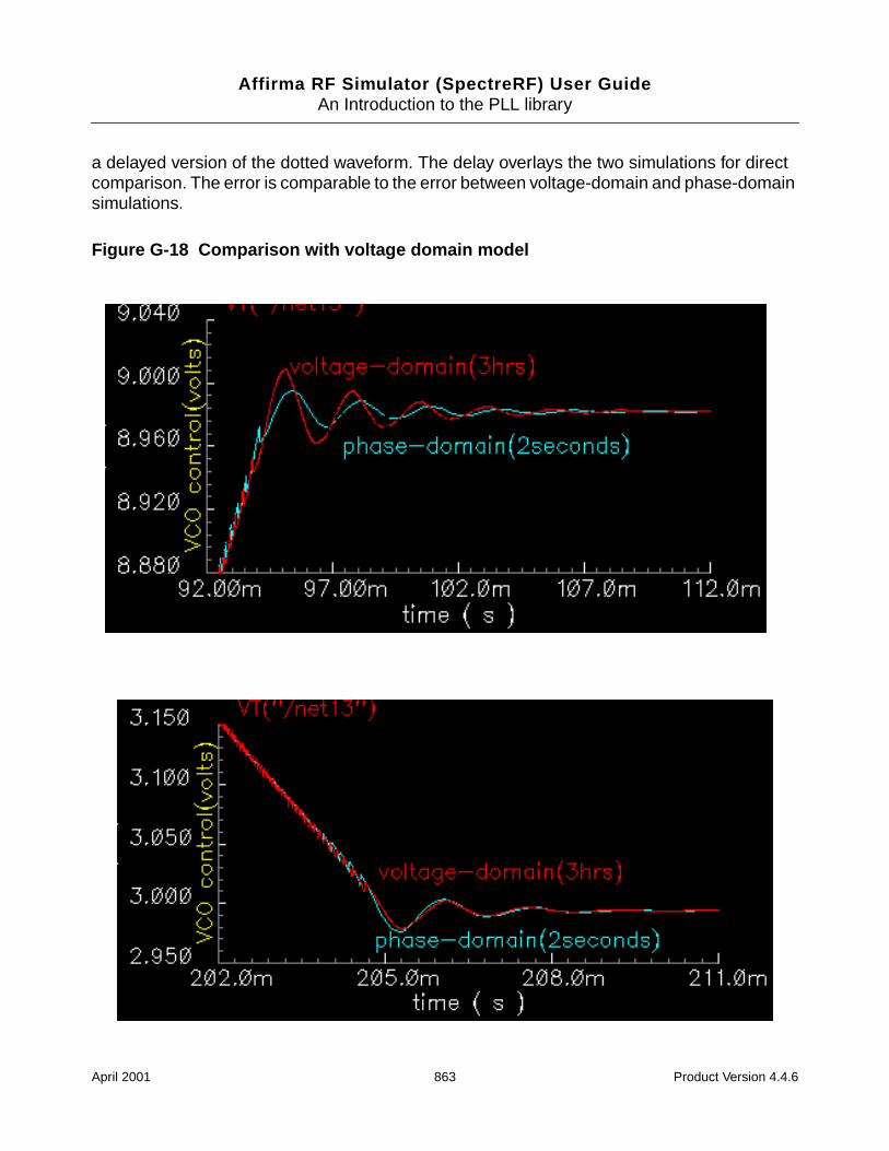
Affirma RF Simulator (SpectreRF) User GuideAn Introduction to the PLL library
a delayed version of the dotted waveform. The delay overlays the two simulations for directcomparison. The error is comparable to the error between voltage-domain and phase-domainsimulations.
Figure G-18 Comparison with voltage domain model
April 2001 863 Product Version 4.4.6
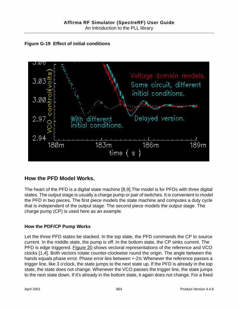
Affirma RF Simulator (SpectreRF) User GuideAn Introduction to the PLL library
Figure G-19 Effect of initial conditions
How the PFD Model Works.
The heart of the PFD is a digital state machine [8,9].The model is for PFDs with three digitalstates. The output stage is usually a charge pump or pair of switches. It is convenient to modelthe PFD in two pieces. The first piece models the state machine and computes a duty cyclethat is independent of the output stage. The second piece models the output stage. Thecharge pump (CP) is used here as an example.
How the PDF/CP Pump Works
Let the three PFD states be stacked. In the top state, the PFD commands the CP to sourcecurrent. In the middle state, the pump is off. In the bottom state, the CP sinks current. ThePFD is edge triggered. Figure 20 shows vectoral representations of the reference and VCOclocks [1,4]. Both vectors rotate counter-clockwise round the origin. The angle between thehands equals phase error. Phase error lies between +-2π. Whenever the reference passes atrigger line, like 3 o'clock, the state jumps to the next state up. If the PFD is already in the topstate, the state does not change. Whenever the VCO passes the trigger line, the state jumpsto the next state down. If it's already in the bottom state, it again does not change. For a fixed
April 2001 864 Product Version 4.4.6
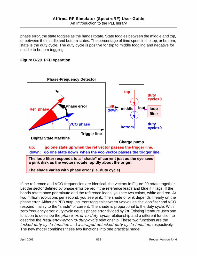
Affirma RF Simulator (SpectreRF) User GuideAn Introduction to the PLL library
phase error, the state toggles as the hands rotate. State toggles between the middle and top,or between the middle and bottom states. The percentage of time spent in the top, or bottom,state is the duty cycle. The duty cycle is positive for top to middle toggling and negative formiddle to bottom toggling.
Figure G-20 PFD operation
If the reference and VCO frequencies are identical, the vectors in Figure 20 rotate together.Let the sector defined by phase error be red if the reference leads and blue if it lags. If thehands rotate once per minute and the reference leads, you see two colors, white and red. Attwo million revolutions per second, you see pink. The shade of pink depends linearly on thephase error. Although PFD output current toggles between two values, the loop filter and VCOrespond mainly to the “shade” of current. The shade is proportional to the duty cycle. Withzero frequency error, duty cycle equals phase error divided by 2π. Existing literature uses onefunction to describe the phase-error-to-duty-cycle relationship and a different function todescribe the frequency-error-to-duty-cycle relationship. These two functions are thelocked duty cycle function and averaged unlocked duty cycle function, respectively.The new model combines these two functions into one practical model.
Ref phase
VCO phase
Trigger line
Phase errorloopfilter
Digital State MachineCharge pump
top
bottom
updown middle iout
dutycycle>0
dutycycle<0
Phase-Frequency Detector
up: go one state up when the ref vector passes the trigger line.down: go one state down when the vco vector passes the trigger line.
The loop filter responds to a “shade” of current just as the eye seesa pink disk as the vectors rotate rapidly about the origin.
The shade varies with phase error (i.e. duty cycle)
April 2001 865 Product Version 4.4.6
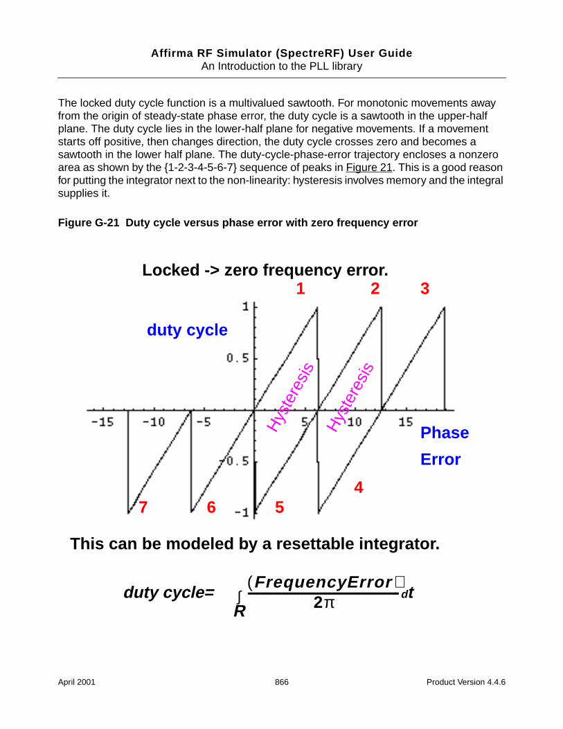
Affirma RF Simulator (SpectreRF) User GuideAn Introduction to the PLL library
The locked duty cycle function is a multivalued sawtooth. For monotonic movements awayfrom the origin of steady-state phase error, the duty cycle is a sawtooth in the upper-halfplane. The duty cycle lies in the lower-half plane for negative movements. If a movementstarts off positive, then changes direction, the duty cycle crosses zero and becomes asawtooth in the lower half plane. The duty-cycle-phase-error trajectory encloses a nonzeroarea as shown by the 1-2-3-4-5-6-7 sequence of peaks in Figure 21. This is a good reasonfor putting the integrator next to the non-linearity: hysteresis involves memory and the integralsupplies it.
Figure G-21 Duty cycle versus phase error with zero frequency error
1 2 3
4567
Phase
Error
duty cycle
Locked -> zero frequency error.H
yste
resi
s
Hys
tere
sis
This can be modeled by a resettable integrator.
duty cycle=FrequencyError( )
2π------------------------------------------------------- td
R∫
April 2001 866 Product Version 4.4.6

Affirma RF Simulator (SpectreRF) User GuideAn Introduction to the PLL library
The new model operates only on frequency error. For small-frequency errors, the duty cycleis indeed proportional to the phase error. The phase error is the integral, with respect to time,of the frequency error. The duty cycle therefore equals the integral of the frequency errordivided by 2π. Resetting the integral whenever it hits +-2π produces the multivalued sawtoothdescribed above. If the frequency error changes sign, the resetting integrator ramps to zero,passes through zero, and generates a sawtooth in the lower-half plane. The phase-error-duty-cycle trajectory is precisely the multivalued sawtooth described above. The resettableintegrator (RI) merges the integrator of a phase-domain model with the locked duty-cyclefunction.
For a sustained frequency error, the RI model predicts an average duty cycle of +-1/2regardless of error size. This is correct only for small-frequency errors. The true duty cyclegoes to +-1 for large-frequency errors. Let the reference frequency far exceed VCOfrequency. Whenever the VCO passes the trigger line, the reference frequency passes shortlythereafter. The reference frequency might pass the trigger line several more times before theVCO passes again. In this case, the phase error is still a sawtooth, but the average duty cycleis nearly 1. This behavior lets the PLL acquire input signals faster. The function H, in Figure22 below, shows the averaged unlocked duty cycle. This cycle depends on the ratio of thereference to VCO frequencies and is discontinuous where frequency error is zero.
April 2001 867 Product Version 4.4.6
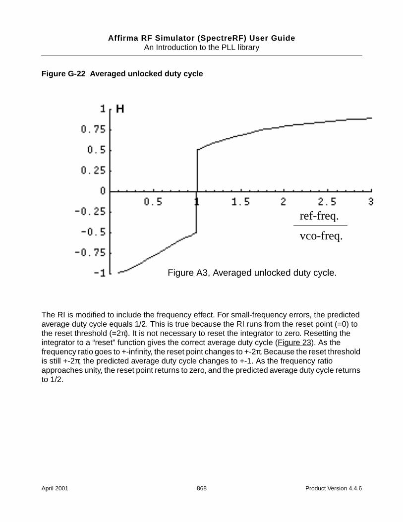
Affirma RF Simulator (SpectreRF) User GuideAn Introduction to the PLL library
Figure G-22 Averaged unlocked duty cycle
The RI is modified to include the frequency effect. For small-frequency errors, the predictedaverage duty cycle equals 1/2. This is true because the RI runs from the reset point (=0) tothe reset threshold (=2π). It is not necessary to reset the integrator to zero. Resetting theintegrator to a “reset” function gives the correct average duty cycle (Figure 23). As thefrequency ratio goes to +-infinity, the reset point changes to +-2π. Because the reset thresholdis still +-2π, the predicted average duty cycle changes to +-1. As the frequency ratioapproaches unity, the reset point returns to zero, and the predicted average duty cycle returnsto 1/2.
H
ref-freq.
vco-freq.
Figure A3, Averaged unlocked duty cycle.
April 2001 868 Product Version 4.4.6
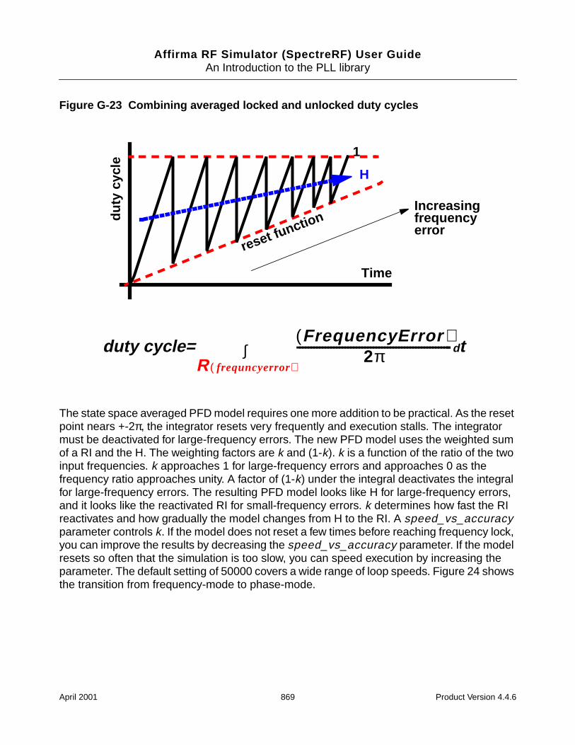
Affirma RF Simulator (SpectreRF) User GuideAn Introduction to the PLL library
Figure G-23 Combining averaged locked and unlocked duty cycles
The state space averaged PFD model requires one more addition to be practical. As the resetpoint nears +-2π, the integrator resets very frequently and execution stalls. The integratormust be deactivated for large-frequency errors. The new PFD model uses the weighted sumof a RI and the H. The weighting factors are k and (1-k). k is a function of the ratio of the twoinput frequencies. k approaches 1 for large-frequency errors and approaches 0 as thefrequency ratio approaches unity. A factor of (1-k) under the integral deactivates the integralfor large-frequency errors. The resulting PFD model looks like H for large-frequency errors,and it looks like the reactivated RI for small-frequency errors. k determines how fast the RIreactivates and how gradually the model changes from H to the RI. A speed_vs_accuracyparameter controls k. If the model does not reset a few times before reaching frequency lock,you can improve the results by decreasing the speed_vs_accuracy parameter. If the modelresets so often that the simulation is too slow, you can speed execution by increasing theparameter. The default setting of 50000 covers a wide range of loop speeds. Figure 24 showsthe transition from frequency-mode to phase-mode.
1
reset function
Time
duty
cyc
le
Increasingfrequencyerror
H
duty cycle=FrequencyError( )
2π------------------------------------------------------- td
R frequncyerror( )∫
April 2001 869 Product Version 4.4.6
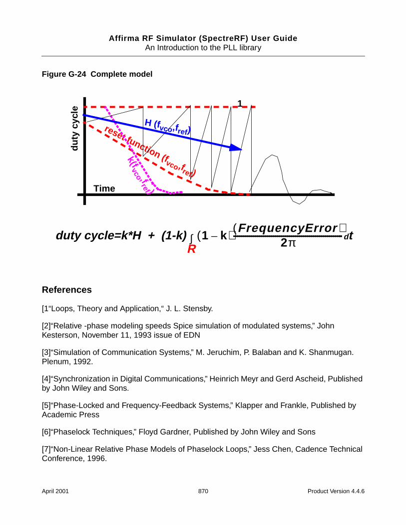
Affirma RF Simulator (SpectreRF) User GuideAn Introduction to the PLL library
Figure G-24 Complete model
References
[1“Loops, Theory and Application,“ J. L. Stensby.
[2]“Relative -phase modeling speeds Spice simulation of modulated systems,” JohnKesterson, November 11, 1993 issue of EDN
[3]“Simulation of Communication Systems,” M. Jeruchim, P. Balaban and K. Shanmugan.Plenum, 1992.
[4]“Synchronization in Digital Communications,” Heinrich Meyr and Gerd Ascheid, Publishedby John Wiley and Sons.
[5]“Phase-Locked and Frequency-Feedback Systems,” Klapper and Frankle, Published byAcademic Press
[6]“Phaselock Techniques,” Floyd Gardner, Published by John Wiley and Sons
[7]“Non-Linear Relative Phase Models of Phaselock Loops,” Jess Chen, Cadence TechnicalConference, 1996.
1
reset function (fvco ,fref )
Time
duty
cyc
le
k(fvco ,fref )
H (fvco ,fref )
duty cycle=k*H + (1-k) 1 k–( ) FrequencyError( )2π------------------------------------------------------- td
R∫
April 2001 870 Product Version 4.4.6

Affirma RF Simulator (SpectreRF) User GuideAn Introduction to the PLL library
[8]“Phase-Locked Loops: Theory, Design, and Applications,” Roland Best, Published byMcGraw-Hill
[9]“Phase-Locked Loop Circuit Design,” Dan Wolaver, Published by Prentice Hall
[10]“Phase-Lock Basics,” Willeam F. Egan. Published by John Wiley and Sons.
[11]“Non-Linear State Space Averaged Modeling of a 3-State Digital Phase-FrequencyDetector,” Jess Chen, Cadence Technical Conference, 1997
[12] “Analog and Mixed-Signal Hardware Description Languages,” Edited by A. Vachoux, J.Berge, O. Levia, and J. Rouillard. Kluwer Academic Publishers.
[13] “Macromodeling with SPICE,” J.A. Connelly and P. Choi. Prentice Hall. Pages 168-169.
[14] S. Cuk, Cal. Inst. of Tech. PhD Thesis, “Modelling, Analysis, and Design of SwitchingConverters.” 1977
April 2001 871 Product Version 4.4.6
Affirma RF Simulator (SpectreRF) User Guide
HUsing port in SpectreRF Simulations
The port component, located in the analogLib library, can be used in RF circuits forSpectreRF and Spectre S-parameter simulations. The port component is similar to theexisting psin, also located in the analogLib library. Unlike psin, port supports all the Sourcetypes of the port primitive in Spectre, specifically: pwl, pulse, sine, dc, and exp.
The port is a resistive source that is tied between positive and negative terminals. It isequivalent to a voltage source in series with a resistor, where the reference resistance of theport is the value of the resistor.
In IC4.4.3_QSR1, port is supported by Spectre Direct netlisting only in the Affirma analogcircuit design environment (spectreS, or Spectre through the cdsSpice socket, is notsupported).
port Capabilities
While the port component is generally useful as a stimulus in high-frequency circuits, it alsohas the following unique capabilities:
Defines the ports of the circuit to the S-parameter analysis
Has an intrinsic noise source that lets the noise analysis directly compute the noisefigure of the circuit
Is the only source for which the amplitude can be specified in terms of power
Terminating the port
When you specify the voltage on a port, Spectre assumes that the port is properlyterminated in it’s reference resistance. The specified voltage value is not the voltage onthe internal voltage source, which is actually set to twice the value specified on the port . Ifyou use a port source to drive an open circuit, the voltage (for DC, transient, AC, and PACsignals) is double its specified value. However, you can alternatively specify the amplitude ofthe sine wave in the transient and PAC analyses as the power in dBm delivered by the portwhen terminated with the reference resistance.
April 2001 872 Product Version 4.4.6
Affirma RF Simulator (SpectreRF) User GuideUsing port in SpectreRF Simulations
port Parameter Types
In this application note, the parameters are grouped by the following types, rather than in theorder they appear on the port Edit Object Properties form.
Port parameters
Resistance
Port number
Multiplier
General waveform parameters
Source type
Delay time
DC Waveform parameters
DC voltage
Pulse waveform parameters
Zero value
One value
Period of waveform
Rise time
Fall time
Pulse width
PWL waveform parameters
Waveform Entry Method
File name
Number of PWL/Time pairs
DC offset
April 2001 873 Product Version 4.4.6
Affirma RF Simulator (SpectreRF) User GuideUsing port in SpectreRF Simulations
Amplitude scale factor
Time scale factor
Breakpoints
Period
Transition Width
Sinusoidal waveform parameters
Sine DC level
Frequency name 1
Frequency 1
Amplitude 1 (Vpk)
Amplitude 1 (dBm)
Phase for Sinusoid 1
Frequency name 2
Frequency 2
Amplitude 2 (Vpk)
Amplitude 2 (dBm)
Phase for Sinusoid 2
Amplitude and Frequency modulation parameters
AM modulation index 1
AM modulation frequency 1
AM modulation phase 1
FM modulation index 1
FM modulation frequency 1
Damping factor 1
April 2001 874 Product Version 4.4.6
Affirma RF Simulator (SpectreRF) User GuideUsing port in SpectreRF Simulations
Exponential waveform parameters
Delay time
Zero value
One value
Rise time start
Rise time constant
Fall time start
Fall time constant
Small-signal parameters
PAC magnitude
PAC magnitude (dBm)
PAC phase
AC magnitude
AC phase
XF magnitude
Temperature effect parameters
Linear temperature coefficient
Quadratic temperature coefficient
Nominal temperature
Noise parameters
Noise Entry Method
Noise file name
Number of noise/freq pairs
April 2001 875 Product Version 4.4.6
Affirma RF Simulator (SpectreRF) User GuideUsing port in SpectreRF Simulations
Port Parameters
Port parameters include Resistance, Port Number, and Multiplier.
Resistance
The reference resistance of the system. The value must be a real number, but not 0. Default:50 Units: Ω
Port number
The number of the port. The value must be a nonzero integer. Each port in a schematic musthave a different Port number. The Port number is not automatically indexed when you placeeach port on your schematic.
Multiplier
The multiplicity factor. The value must be a nonzero real number. This number lets you specifya number of ports in parallel. For example, if you set Resistance to 50 and Multiplier to2, you specify two ports in parallel, with an effective reference resistance of 25 Ω. Default: 1
General Waveform Parameters
Source type
The Source type parameter lets you specify the parameters for several different waveshapes and then quickly switch between them without losing the settings. Possible values forSource type are: dc, pulse, exp, pwl, sine, or blank. The typical Source types used inSpectreRF analyses are dc, pulse, and sine. For example, you can quickly switch from asinusoid level (for PSS analysis) to a DC level (for PAC analysis) by changing the Sourcetype from sine to dc in the Edit Object Properties form.
If you set Source type to a blank value, the port acts as a resistive load.
April 2001 876 Product Version 4.4.6
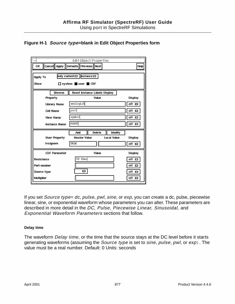
Affirma RF Simulator (SpectreRF) User GuideUsing port in SpectreRF Simulations
Figure H-1 Source type =blank in Edit Object Properties form
If you set Source type= dc, pulse, pwl, sine, or exp, you can create a dc, pulse, piecewiselinear, sine, or exponential waveform whose parameters you can alter. These parameters aredescribed in more detail in the DC, Pulse, Piecewise Linear, Sinusoidal, andExponential Waveform Parameters sections that follow.
Delay time
The waveform Delay time, or the time that the source stays at the DC level before it startsgenerating waveforms (assuming the Source type is set to sine, pulse, pwl, or exp) . Thevalue must be a real number. Default: 0 Units: seconds
April 2001 877 Product Version 4.4.6

Affirma RF Simulator (SpectreRF) User GuideUsing port in SpectreRF Simulations
DC Waveform Parameters
To generate a dc waveform from the port component, set the CDF parameter Sourcetype=dc as shown in the figure below. When Source type=dc, the dc and temperature effectparameters are active and set the DC level for all analyses. In DC analysis, this setting alsodetermines the DC level generated by the source, regardless of what Source type youspecify.
DC voltage
Sets the DC level of the source for DC analysis. The value must be a real number. If you donot specify the DC value, it is assumed to be the time =0 value of the waveform. Default: 0Units: V
The DC voltage parameter specifies the DC voltage across the port when it is terminated inits reference resistance. In other words, the DC voltage of the internal voltage source isdouble the user specified DC value, dc. The same is true for the values for the transient, AC,and PAC signals of the port . However, you can alternatively specify the amplitude of the sinewave in the transient and PAC analyses as the power in dBm delivered by the port when it isterminated with the reference resistance.
Because all small signal analyses (AC, XF, and Noise) use DC analysis results, the DCvoltage level also affects small-signal analyses. Transient analysis is not affected unlessyou specify Source type=dc or use dc as a default for the other waveform types.
April 2001 878 Product Version 4.4.6
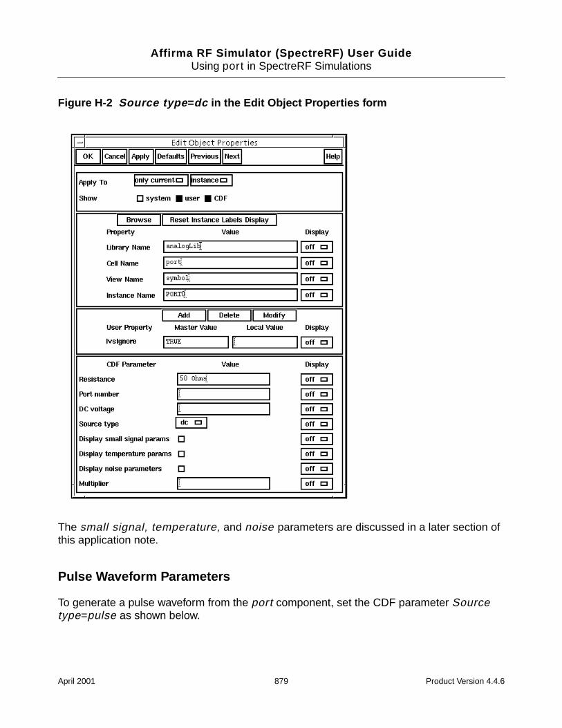
Affirma RF Simulator (SpectreRF) User GuideUsing port in SpectreRF Simulations
Figure H-2 Source type =dc in the Edit Object Properties form
The small signal, temperature, and noise parameters are discussed in a later section ofthis application note.
Pulse Waveform Parameters
To generate a pulse waveform from the port component, set the CDF parameter Sourcetype=pulse as shown below.
April 2001 879 Product Version 4.4.6
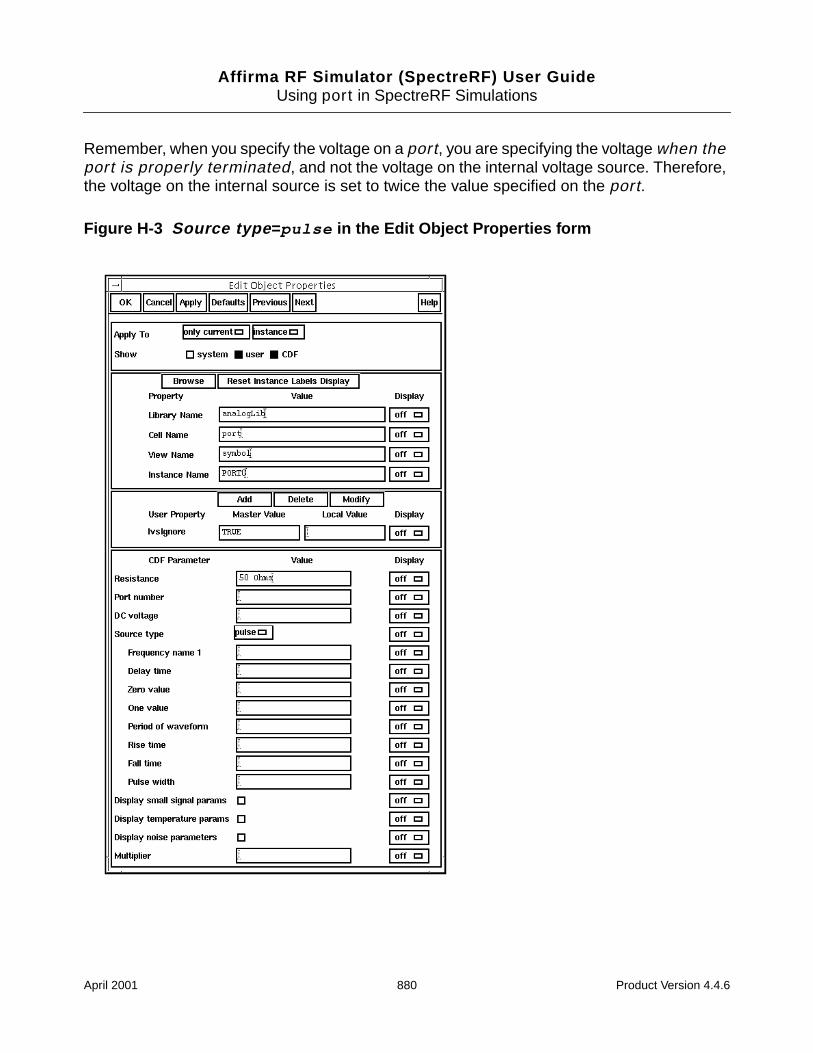
Affirma RF Simulator (SpectreRF) User GuideUsing port in SpectreRF Simulations
Remember, when you specify the voltage on a port, you are specifying the voltage when theport is properly terminated, and not the voltage on the internal voltage source. Therefore,the voltage on the internal source is set to twice the value specified on the port.
Figure H-3 Source type =pulse in the Edit Object Properties form
April 2001 880 Product Version 4.4.6
Affirma RF Simulator (SpectreRF) User GuideUsing port in SpectreRF Simulations
Zero value
The Zero value (val0) used in pulse and exp waveforms. Default: 0 Units: V
One value
The One value (val1) used in pulse and exp waveforms. Default: 1 Units: V
Period of waveform
The period of the pulse waveform. Default: infinity. Units: seconds
Rise time
The Rise time for the pulse waveform (time for transition from the Zero value to the Onevalue). Units: seconds
Fall time
The Fall time for the pulse waveform (time for transition from the One value to the Zerovalue). Units: seconds
Pulse width
Pulse width (width, duration of One value). Default: infinity. Units: seconds
PWL Waveform Parameters
To generate a piecewise linear waveform from the port component, set the CDF parameterSource type=pwl as shown in the next figure.
Remember, when you specify the voltage on a port, you are specifying the voltage when theport is properly terminated, and not the voltage on the internal voltage source. Therefore,the voltage on the internal source is set to twice the value specified on the port.
April 2001 881 Product Version 4.4.6
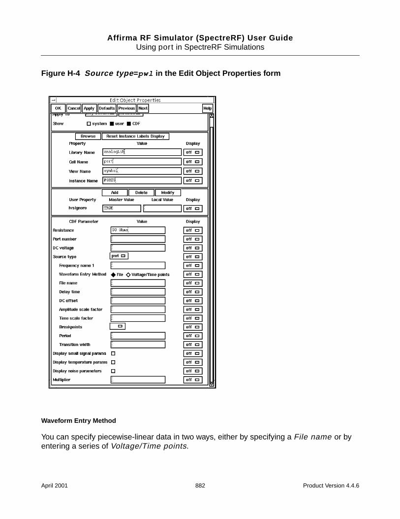
Affirma RF Simulator (SpectreRF) User GuideUsing port in SpectreRF Simulations
Figure H-4 Source type =pwl in the Edit Object Properties form
Waveform Entry Method
You can specify piecewise-linear data in two ways, either by specifying a File name or byentering a series of Voltage/Time points.
April 2001 882 Product Version 4.4.6
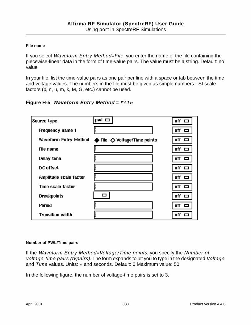
Affirma RF Simulator (SpectreRF) User GuideUsing port in SpectreRF Simulations
File name
If you select Waveform Entry Method=File, you enter the name of the file containing thepiecewise-linear data in the form of time-value pairs. The value must be a string. Default: novalue
In your file, list the time-value pairs as one pair per line with a space or tab between the timeand voltage values. The numbers in the file must be given as simple numbers - SI scalefactors (p, n, u, m, k, M, G, etc.) cannot be used.
Figure H-5 Waveform Entry Method = File
Number of PWL/Time pairs
If the Waveform Entry Method=Voltage/Time points, you specify the Number ofvoltage-time pairs (tvpairs). The form expands to let you to type in the designated Voltageand Time values. Units: V and seconds. Default: 0 Maximum value: 50
In the following figure, the number of voltage-time pairs is set to 3.
April 2001 883 Product Version 4.4.6
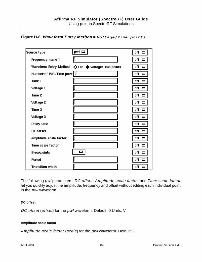
Affirma RF Simulator (SpectreRF) User GuideUsing port in SpectreRF Simulations
Figure H-6 Waveform Entry Method = Voltage/Time points
The following pwl parameters: DC offset, Amplitude scale factor, and Time scale factorlet you quickly adjust the amplitude, frequency and offset without editing each individual pointin the pwl waveform.
DC offset
DC offset (offset) for the pwl waveform. Default: 0 Units: V
Amplitude scale factor
Amplitude scale factor (scale) for the pwl waveform. Default: 1
April 2001 884 Product Version 4.4.6
Affirma RF Simulator (SpectreRF) User GuideUsing port in SpectreRF Simulations
Time scale factor
Time scale factor (stretch) for the time given for the pwl waveform. Default: 1
Breakpoints
Possible values are no, yes, or blank. If you set Breakpoints (allbrkpts) to yes, you forceSpectre to place time points at each point specified in a pwl waveform during a transientanalysis. This can be very expensive for waveforms with many points. If you set Breakpointsto no, Spectre inspects the waveform, looking for abrupt changes, and forces time points onlyat those changes. If you set Source type = pwl and set Breakpoints to blank, the default isyes if the number of points you specify is less than 20.
Period
The pwl waveform is periodic if you specify Period (pwlperiod). Units: seconds
If the value of the waveform you specify is not exactly the same at both its beginning and itsend, then you must provide a nonzero value for Transition Width.
Transition Width
Transition width (twidth) is used when making pwl waveforms periodic. Default: PWLperiod/1000. Units: seconds
Before repeating, the waveform changes linearly in an interval of Transition Width from itsvalue at (Period – Transition Width) to its value at the beginning of the waveform. Thus theTransition Width must always be less than the Period.
Sinusoidal Waveform Parameters
The port component can generate up to two sinusoids simultaneously. They are denoted as1 and 2. You can set the amplitude, frequency and phase for both individually. The amplitudecan be set to either a voltage or a power level. You can also specify sinusoidal AM or FMmodulation of sinusoid 1.
The Edit Object Properties form for Source type=sine is shown below.
The first sinusoid is described by the parameters Frequency name 1, Frequency 1,Amplitude 1 (Vpk), Amplitude 1 (dBm), Phase for sinusoid 1, Sine DC level,AM or FM modulation terms, and Damping factor 1.
April 2001 885 Product Version 4.4.6
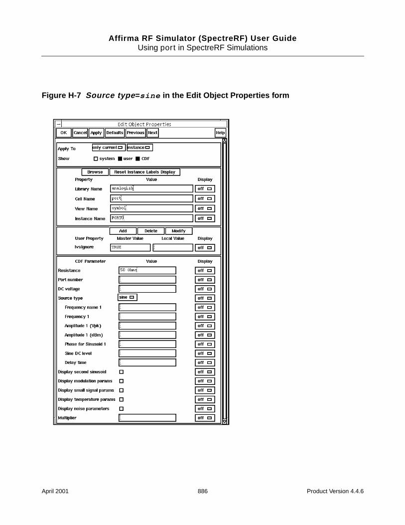
Affirma RF Simulator (SpectreRF) User GuideUsing port in SpectreRF Simulations
Figure H-7 Source type =sine in the Edit Object Properties form
April 2001 886 Product Version 4.4.6
Affirma RF Simulator (SpectreRF) User GuideUsing port in SpectreRF Simulations
Frequency name 1
Names the fundamental tones of sinusoid 1. After you save the schematic, the names youassign appear in the Fundamental Tones list box on the Choosing Analyses form.
Frequency 1
The frequency of the first sinusoidal waveform (carrier frequency). You typically useunmodulated signals in SpectreRF analyses. The value must be a real number. Default: 0Units: Hz
Amplitude 1 (Vpk)
Peak amplitude of the first sinusoidal waveform that you generate. The value specified is thevoltage delivered into a matched load. You can select either Amplitude 1 (Vpk) orAmplitude 1 (dBm), but not both. If Amplitude 1 (Vpk) has a value, the Amplitude 1(dBm) field is grayed out. The value must be a real number. Default: 1 Units: V
Remember, when you specify the voltage on a port, you are specifying the voltage when theport is properly terminated, and not the voltage on the internal voltage source. Thus, thevoltage on the internal source is set to twice the value specified on the port.
Amplitude 1 (dBm)
Amplitude of the first sinusoidal waveform, in dBm. The value specified is the power deliveredinto a matched load. You can select either Amplitude 1 (Vpk) or Amplitude 1 (dBm), butnot both. If Amplitude 1 (dBm) has a value, the Amplitude 1 (Vpk) field is grayed out. Thevalue must be a real number. Units: dBm
Phase for Sinusoid 1
The phase at the specified Delay time. The sinusoidal waveform might start before the givenDelay time in order to achieve a specified phase and still remain continuous. For example, ifyou want to generate a cosine wave, set this parameter to 90o. The value must be a realnumber. Default: 0 Units: degrees
Sine DC level
Sets the DC level for sinusoidal waveforms in transient analyses. This parameter is usedwhen the sinusoid has a different average level than the one specified for the DC analyses. Ifnot specified, the average value of the sinusoid is the same as that of the DC level of thesource. The value must be a real number. Default: dc Units: V
April 2001 887 Product Version 4.4.6
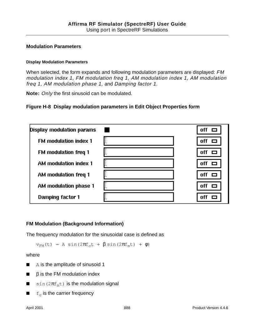
Affirma RF Simulator (SpectreRF) User GuideUsing port in SpectreRF Simulations
Modulation Parameters
Display Modulation Parameters
When selected, the form expands and following modulation parameters are displayed: FMmodulation index 1, FM modulation freq 1, AM modulation index 1, AM modulationfreq 1, AM modulation phase 1, and Damping factor 1.
Note: Only the first sinusoid can be modulated.
Figure H-8 Display modulation parameters in Edit Object Properties form
FM Modulation (Background Information)
The frequency modulation for the sinusoidal case is defined as
vFM(t) = A sin(2 πf ct + β sin(2 πf mt) + φ)
where
A is the amplitude of sinusoid 1
β is the FM modulation index
sin(2 πf mt) is the modulation signal
f c is the carrier frequency
April 2001 888 Product Version 4.4.6
Affirma RF Simulator (SpectreRF) User GuideUsing port in SpectreRF Simulations
φ is the phase for sinusoid 1
The frequency modulation parameters affect only the first sinusoid generated by port. Theyhave no effect on the second sinusoid.
FM modulation frequency 1
FM modulation frequency for the sinusoidal waveform (f m in the previous equation). Thevalue must be a real number. Default: 0 Units: Hz
FM modulation index 1
FM index of modulation for the sinusoidal waveform, the ratio of peak frequency deviationdivided by the center frequency (β in the above equations).
β=∆f/f m
The value must be a real number. Default: 0
Effect of Amplitude Modulation (Background Information)
The amplitude modulation (double sideband suppressed carrier, or DSB-SC) is defined as
vAM(t) = A (1 + m sin(2 πf mt + φ)) sin(2 πf ct)
where
A is the carrier amplitude (amplitude of sinusoid 1)
m is the AM modulation index
f m is the AM modulation frequency
φ is the AM modulation phase
sin(2 πf ct) is the carrier signal
The amplitude modulation parameters affect only the first sinusoid generated by port. Theyhave no effect on the second sinusoid.
AM modulation frequency 1
AM modulation frequency for the first sinusoidal waveform (f min the previous equation). Thevalue must be a real number. Default: 0 Units: Hz
April 2001 889 Product Version 4.4.6
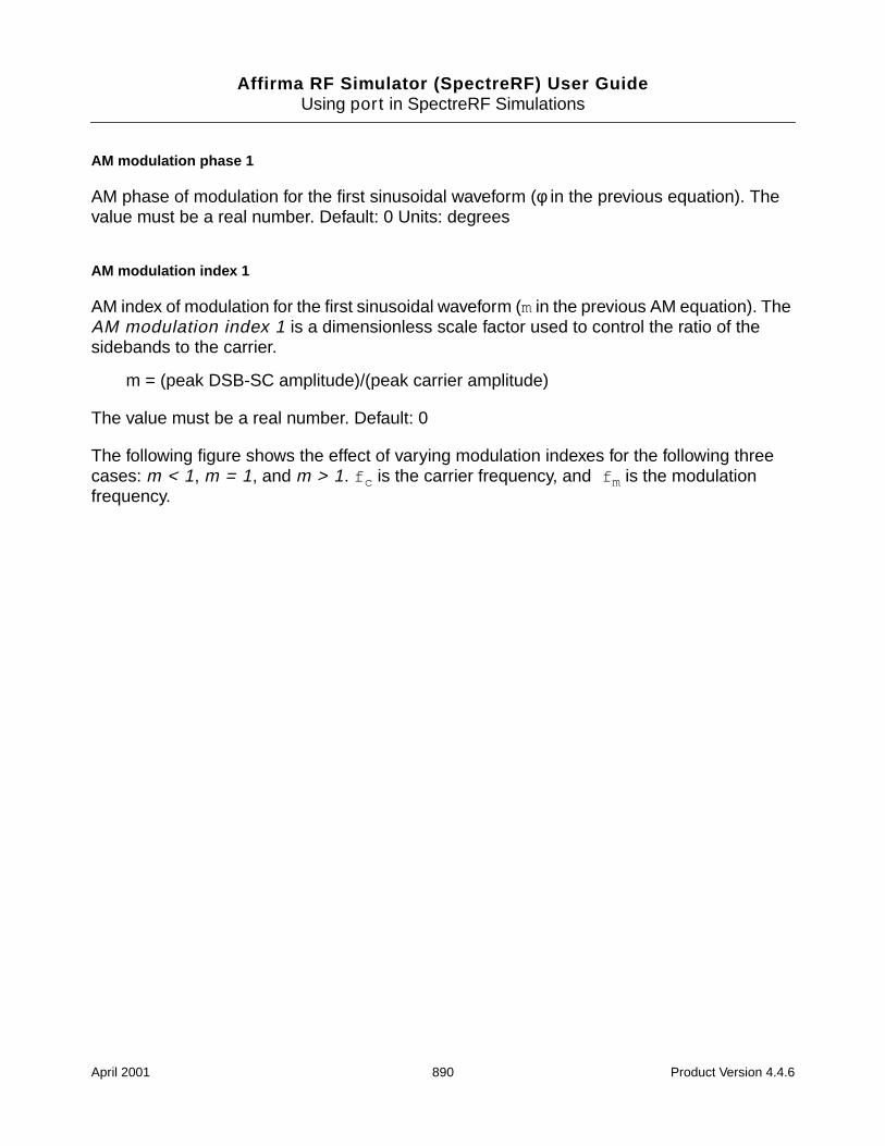
Affirma RF Simulator (SpectreRF) User GuideUsing port in SpectreRF Simulations
AM modulation phase 1
AM phase of modulation for the first sinusoidal waveform (φ in the previous equation). Thevalue must be a real number. Default: 0 Units: degrees
AM modulation index 1
AM index of modulation for the first sinusoidal waveform (min the previous AM equation). TheAM modulation index 1 is a dimensionless scale factor used to control the ratio of thesidebands to the carrier.
m = (peak DSB-SC amplitude)/(peak carrier amplitude)
The value must be a real number. Default: 0
The following figure shows the effect of varying modulation indexes for the following threecases: m < 1, m = 1, and m > 1. f c is the carrier frequency, and f m is the modulationfrequency.
April 2001 890 Product Version 4.4.6
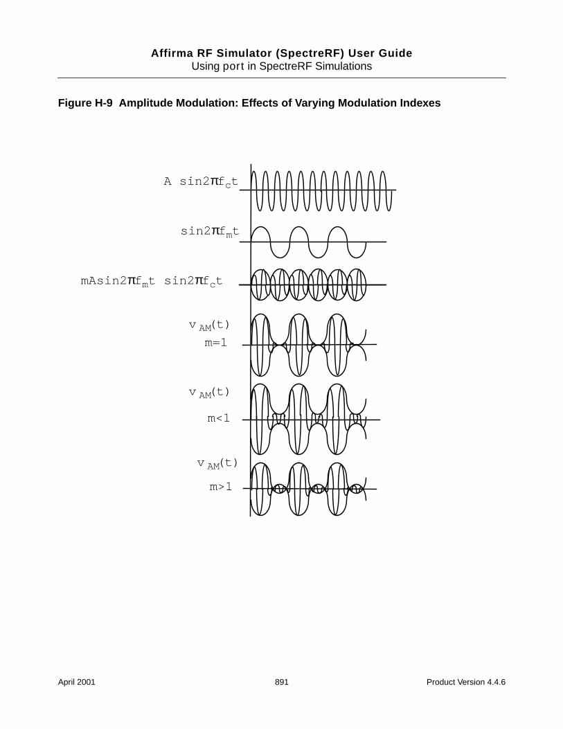
Affirma RF Simulator (SpectreRF) User GuideUsing port in SpectreRF Simulations
Figure H-9 Amplitude Modulation: Effects of Varying Modulation Indexes
v AM(t)
v AM(t)
v AM(t)
m>1
m=1
m<1
A sin2 πf ct
sin2 πf mt
mAsin2 πf mt sin2 πf ct
April 2001 891 Product Version 4.4.6

Affirma RF Simulator (SpectreRF) User GuideUsing port in SpectreRF Simulations
Damping factor 1
Damping factor for the sinusoidal waveform. Damping factor 1specifies the time it takes to gofrom the envelope (full amplitude) at time=0 to 63 percent of the full amplitude. For example,consider the following damped sinusoid:
v(t) = A e −σt sin(2 πft + φ)
where
σ = Damping factor 1, A is the amplitude of sinusoid 1, and φ is the Phase for sinusoid 1
If σ = 0 , the waveform is a pure sinusoid (steady state).
If σ < 0 , the waveform exhibits decaying oscillations.
If σ > 0 , the waveform exhibits growing oscillations.
It takes 5σ to diminish to 1 percent of the peak amplitude. The value must be a real number.Default: 0. Units: 1/seconds
The following figure shows the effect of Damping factor 1 on the first sinusoid for threevalues of σ.
April 2001 892 Product Version 4.4.6
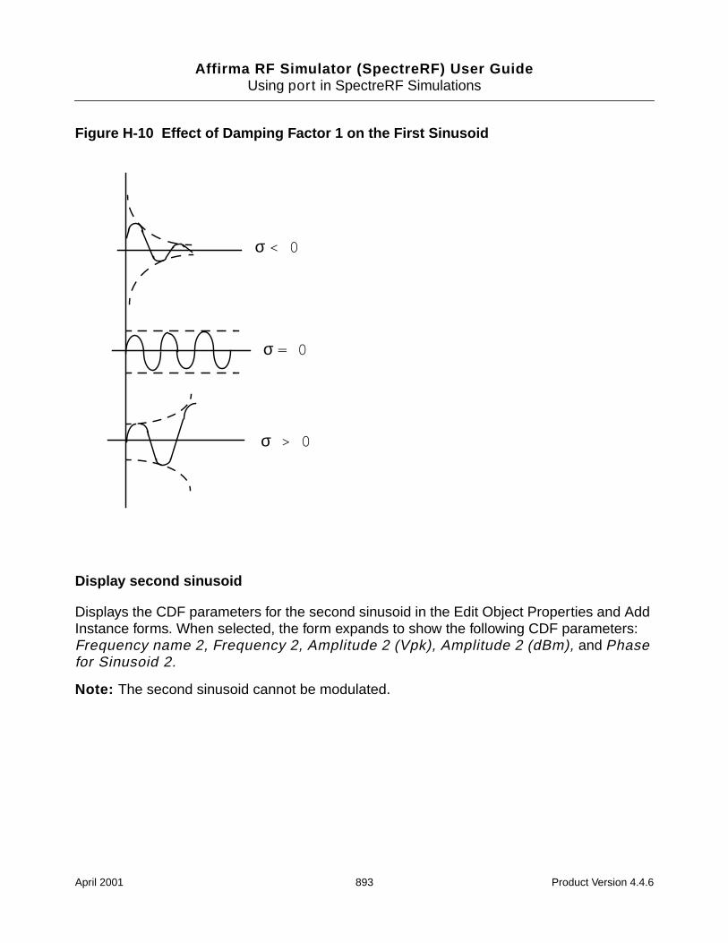
Affirma RF Simulator (SpectreRF) User GuideUsing port in SpectreRF Simulations
Figure H-10 Effect of Damping Factor 1 on the First Sinusoid
Display second sinusoid
Displays the CDF parameters for the second sinusoid in the Edit Object Properties and AddInstance forms. When selected, the form expands to show the following CDF parameters:Frequency name 2, Frequency 2, Amplitude 2 (Vpk), Amplitude 2 (dBm), and Phasefor Sinusoid 2.
Note: The second sinusoid cannot be modulated.
σ = 0
σ < 0
σ > 0
April 2001 893 Product Version 4.4.6
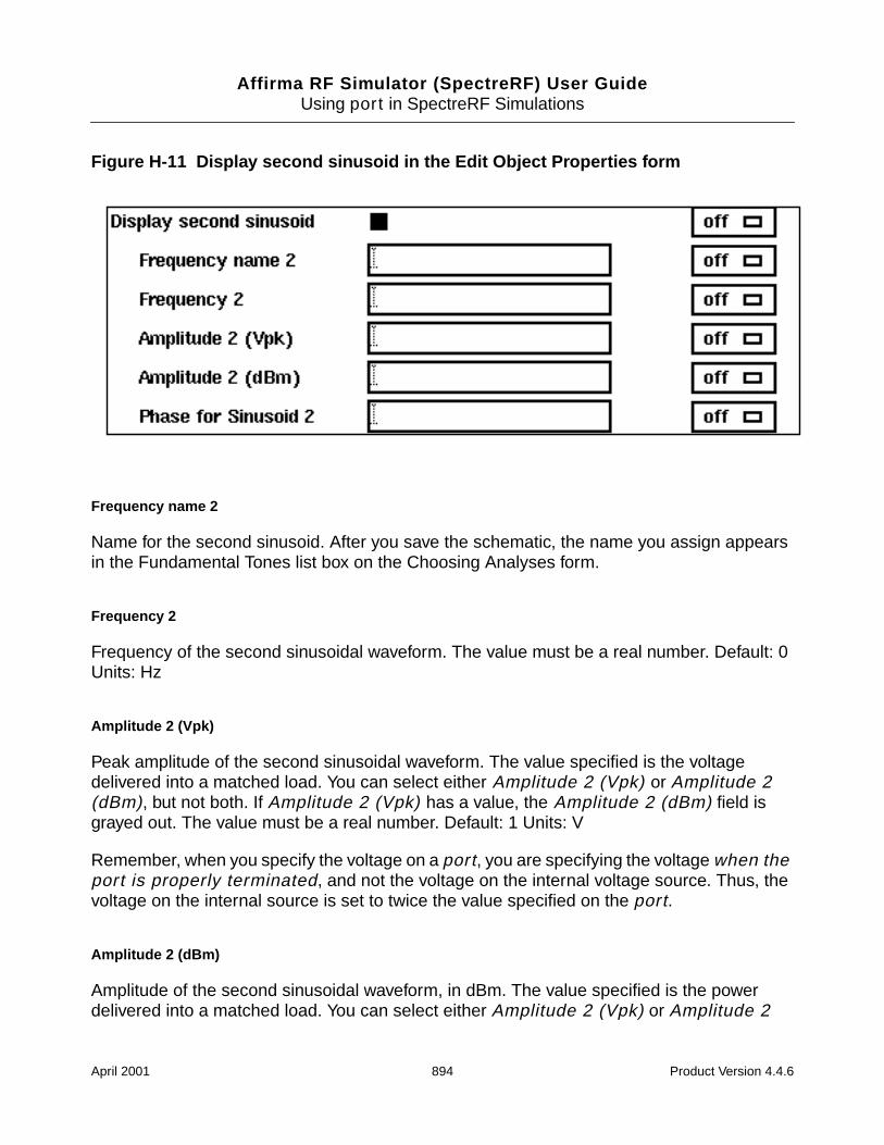
Affirma RF Simulator (SpectreRF) User GuideUsing port in SpectreRF Simulations
Figure H-11 Display second sinusoid in the Edit Object Properties form
Frequency name 2
Name for the second sinusoid. After you save the schematic, the name you assign appearsin the Fundamental Tones list box on the Choosing Analyses form.
Frequency 2
Frequency of the second sinusoidal waveform. The value must be a real number. Default: 0Units: Hz
Amplitude 2 (Vpk)
Peak amplitude of the second sinusoidal waveform. The value specified is the voltagedelivered into a matched load. You can select either Amplitude 2 (Vpk) or Amplitude 2(dBm), but not both. If Amplitude 2 (Vpk) has a value, the Amplitude 2 (dBm) field isgrayed out. The value must be a real number. Default: 1 Units: V
Remember, when you specify the voltage on a port, you are specifying the voltage when theport is properly terminated, and not the voltage on the internal voltage source. Thus, thevoltage on the internal source is set to twice the value specified on the port.
Amplitude 2 (dBm)
Amplitude of the second sinusoidal waveform, in dBm. The value specified is the powerdelivered into a matched load. You can select either Amplitude 2 (Vpk) or Amplitude 2
April 2001 894 Product Version 4.4.6
Affirma RF Simulator (SpectreRF) User GuideUsing port in SpectreRF Simulations
(dBm), but not both. If Amplitude 2 (dBm) has a value, the Amplitude 2 (Vpk) field isgrayed out. The value must be a real number. Units: dBm
Phase for Sinusoid 2
The phase at the specified Delay time for the second sinusoid. The sinusoidal waveformmight start before the given Delay time in order to achieve specified phase while stillremaining continuous. The value must be a real number. Default: 0 Units: degrees
Exponential Waveform Parameters
To generate an exponential waveforms from the port component, set the CDF parameterSource type=exp, as shown in the next figure.
April 2001 895 Product Version 4.4.6
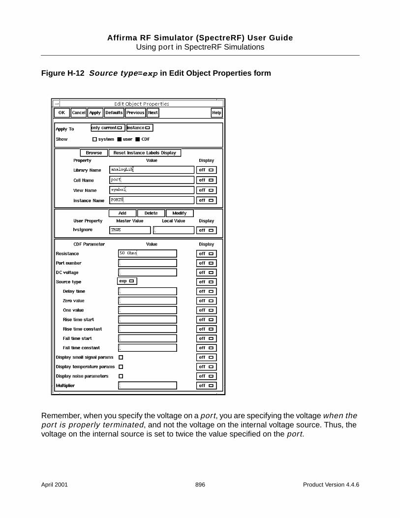
Affirma RF Simulator (SpectreRF) User GuideUsing port in SpectreRF Simulations
Figure H-12 Source type =exp in Edit Object Properties form
Remember, when you specify the voltage on a port, you are specifying the voltage when theport is properly terminated, and not the voltage on the internal voltage source. Thus, thevoltage on the internal source is set to twice the value specified on the port.
April 2001 896 Product Version 4.4.6
Affirma RF Simulator (SpectreRF) User GuideUsing port in SpectreRF Simulations
Zero value
The Zero value (val0) used in pulse and exp waveforms. Default: 0 Units: V
One value
The One value (val1) used in pulse and exp waveforms. Default: 1 Units: V
Rise time start
Rise start time (td1) for the exp waveform. Default: 0 Units: seconds
Rise time constant
Rise time constant (tau1) for the exp waveform. Units: seconds
Fall time start
Fall start time (td2) for the exp waveform. Units: seconds
Fall time constant
Fall time constant (tau2) for the exp waveform. Units: seconds
April 2001 897 Product Version 4.4.6
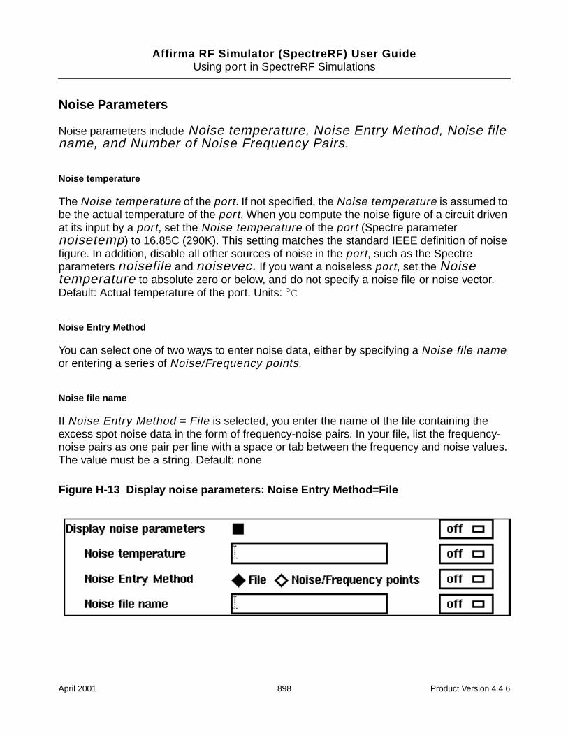
Affirma RF Simulator (SpectreRF) User GuideUsing port in SpectreRF Simulations
Noise Parameters
Noise parameters include Noise temperature, Noise Entry Method, Noise filename, and Number of Noise Frequency Pairs.
Noise temperature
The Noise temperature of the port. If not specified, the Noise temperature is assumed tobe the actual temperature of the port. When you compute the noise figure of a circuit drivenat its input by a port, set the Noise temperature of the port (Spectre parameternoisetemp) to 16.85C (290K). This setting matches the standard IEEE definition of noisefigure. In addition, disable all other sources of noise in the port, such as the Spectreparameters noisefile and noisevec. If you want a noiseless port, set the Noisetemperature to absolute zero or below, and do not specify a noise file or noise vector.Default: Actual temperature of the port. Units: oC
Noise Entry Method
You can select one of two ways to enter noise data, either by specifying a Noise file nameor entering a series of Noise/Frequency points.
Noise file name
If Noise Entry Method = File is selected, you enter the name of the file containing theexcess spot noise data in the form of frequency-noise pairs. In your file, list the frequency-noise pairs as one pair per line with a space or tab between the frequency and noise values.The value must be a string. Default: none
Figure H-13 Display noise parameters: Noise Entry Method=File
April 2001 898 Product Version 4.4.6
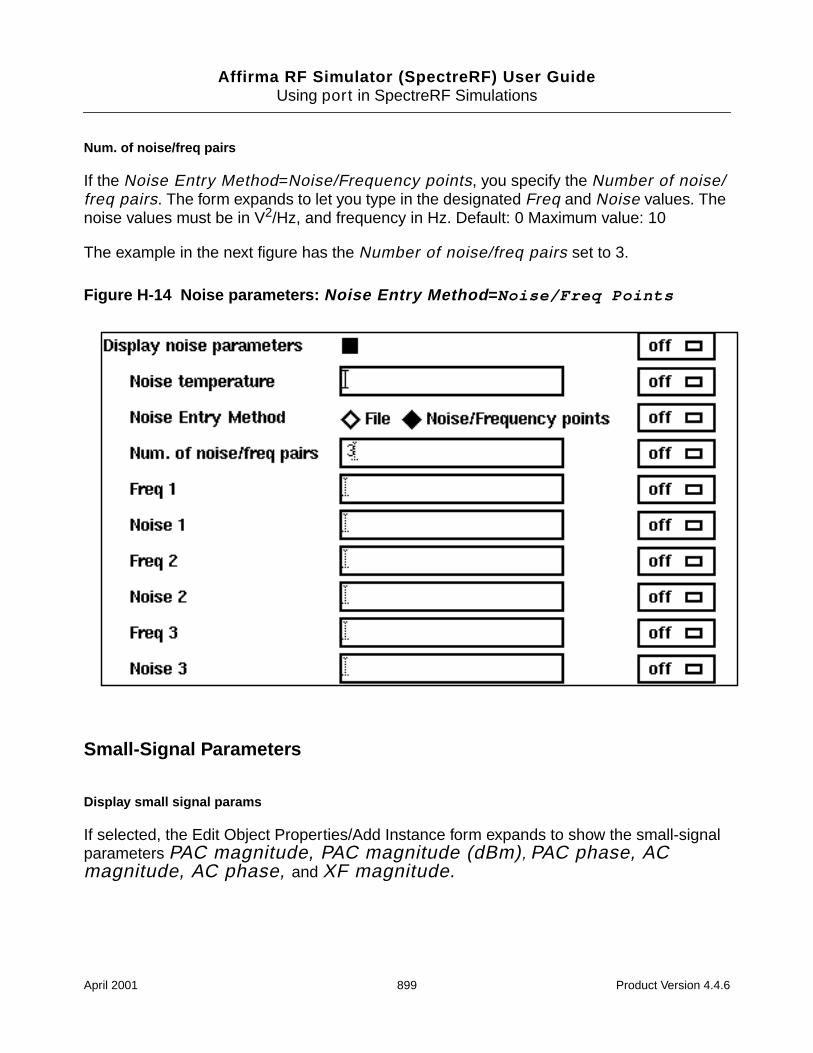
Affirma RF Simulator (SpectreRF) User GuideUsing port in SpectreRF Simulations
Num. of noise/freq pairs
If the Noise Entry Method=Noise/Frequency points, you specify the Number of noise/freq pairs. The form expands to let you type in the designated Freq and Noise values. Thenoise values must be in V2/Hz, and frequency in Hz. Default: 0 Maximum value: 10
The example in the next figure has the Number of noise/freq pairs set to 3.
Figure H-14 Noise parameters: Noise Entry Method =Noise/Freq Points
Small-Signal Parameters
Display small signal params
If selected, the Edit Object Properties/Add Instance form expands to show the small-signalparameters PAC magnitude, PAC magnitude (dBm), PAC phase, ACmagnitude, AC phase, and XF magnitude.
April 2001 899 Product Version 4.4.6
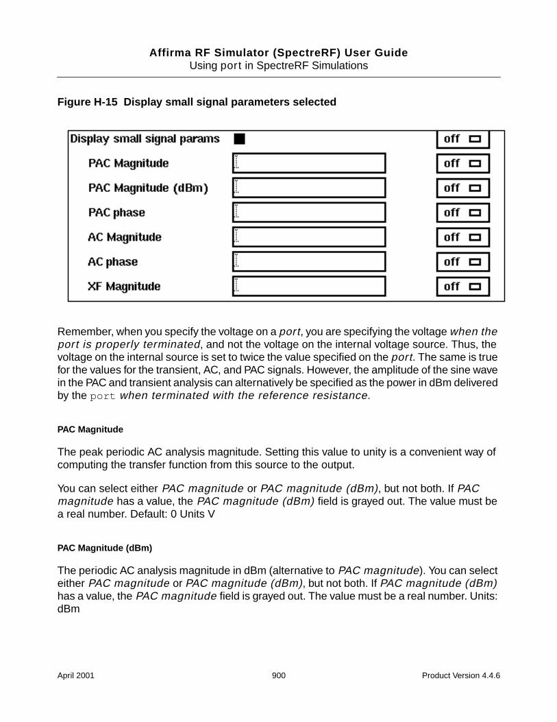
Affirma RF Simulator (SpectreRF) User GuideUsing port in SpectreRF Simulations
Figure H-15 Display small signal parameters selected
Remember, when you specify the voltage on a port, you are specifying the voltage when theport is properly terminated, and not the voltage on the internal voltage source. Thus, thevoltage on the internal source is set to twice the value specified on the port. The same is truefor the values for the transient, AC, and PAC signals. However, the amplitude of the sine wavein the PAC and transient analysis can alternatively be specified as the power in dBm deliveredby the port when terminated with the reference resistance.
PAC Magnitude
The peak periodic AC analysis magnitude. Setting this value to unity is a convenient way ofcomputing the transfer function from this source to the output.
You can select either PAC magnitude or PAC magnitude (dBm), but not both. If PACmagnitude has a value, the PAC magnitude (dBm) field is grayed out. The value must bea real number. Default: 0 Units V
PAC Magnitude (dBm)
The periodic AC analysis magnitude in dBm (alternative to PAC magnitude). You can selecteither PAC magnitude or PAC magnitude (dBm), but not both. If PAC magnitude (dBm)has a value, the PAC magnitude field is grayed out. The value must be a real number. Units:dBm
April 2001 900 Product Version 4.4.6
Affirma RF Simulator (SpectreRF) User GuideUsing port in SpectreRF Simulations
PAC phase
The periodic AC analysis phase. The value must be a real number. Default: 0 Units: degrees
Typically, only one source in the circuit has a PAC magnitude set to a value other than zero,and usually it has a PAC magnitude=1 and PAC phase=0. However, there are situationswhere more than one source has a nonzero PAC magnitude. For example, applying adifferential small-signal input could be done with two sources with the PAC magnitudes setto 0.5 and the PAC phases set to 0 and 180.
You do not specify the PAC frequency in the port Edit Object Properties form. Instead, youset the PAC frequency in the PAC Choosing Analysis form. For example, when making anIP3 measurement, you set the PAC frequency to a variable value in the Choosing AnalysisForm. Then, you enter the same variable in the PAC Amplitude (or PAC AmplitudedBm) field of the port Edit Object Properties form.
AC Magnitude
The peak small-signal voltage. The value must be a real number. Default: 0 Units: V
AC phase
The small-signal phase. The value must be a real number. Default: 0 Units: degrees
Typically, only one source in the circuit has AC Magnitude set to a value other than zero, andusually it has an AC magnitude=1 and AC phase=0. However, there are situations wheremore than one source has a nonzero AC magnitude. For example, you can apply adifferential small-signal input with two sources with the AC magnitudes set to 0.5 and theAC phases set to 0 and 180.
XF Magnitude
The transfer function analysis magnitude. Use XF magnitude to compensate for gain orloss in the test fixture. The value must be a real number. Default: 1 Units: V/V
April 2001 901 Product Version 4.4.6
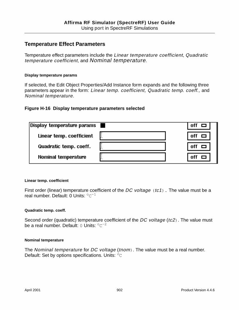
Affirma RF Simulator (SpectreRF) User GuideUsing port in SpectreRF Simulations
Temperature Effect Parameters
Temperature effect parameters include the Linear temperature coefficient, Quadratictemperature coefficient, and Nominal temperature.
Display temperature params
If selected, the Edit Object Properties/Add Instance form expands and the following threeparameters appear in the form: Linear temp. coefficient, Quadratic temp. coeff., andNominal temperature.
Figure H-16 Display temperature parameters selected
Linear temp. coefficient
First order (linear) temperature coefficient of the DC voltage ( tc1). The value must be areal number. Default: 0 Units: oC-1
Quadratic temp. coeff.
Second order (quadratic) temperature coefficient of the DC voltage (tc2) . The value mustbe a real number. Default: 0 Units: oC-2
Nominal temperature
The Nominal temperature for DC voltage (tnom) . The value must be a real number.Default: Set by options specifications. Units: oC
April 2001 902 Product Version 4.4.6
Affirma RF Simulator (SpectreRF) User GuideUsing port in SpectreRF Simulations
How Temperature Parameters Affect the Voltage Level (Background Information)
The value of the DC voltage can vary as a function of the temperature if you specify tc1 andtc2. The variation is given by
VDC( T) = dc * [1 + tc1 * ( T – tnom) + tc2 * ( T – tnom) 2]
where T is the analysis temperature specified in the analysis options, tnom is the Nominaltemperature specified in the Choosing Analyses form, and dc is the DC voltage.
If the analysis temperature equals the nominal temperature, the result is the voltageamplitude that you specified, V(T)=dc.
If the nominal and analysis temperatures differ, the voltage amplitude is given by
VDC( T) = dc * [1 + tc1 * ( T – tnom) + tc2 * ( T – tnom) 2]
where T is the analysis temperature you specify in the analysis options and tnom is thenominal temperature, tc1 and tc2 are the Linear and Quadratic temperaturecoefficients, and dc is the DC voltage.
For example, if the Nominal temperature is 27oC and the analysis temperature is 25oC,there is a 2o difference between the nominal and analysis temperature. The voltage amplitudeis
VDC( T) = dc * [1 + tc1 * (–2) + tc2 * (–2) 2]
Additional Notes
Active Parameters in Analyses
In DC analyses, the only active parameters are dc, m, and the temperature coefficientparameters.
In AC analyses, the only active parameters are m, mag, and phase.
In transient analyses, all parameters are active except the small-signal parameters and thenoise parameters.
In PAC, the only active parameters are m, PAC magnitude (amplitude or dBm), and PACphase.
XF magnitude is active in XF and PXF analyses only.
April 2001 903 Product Version 4.4.6
Affirma RF Simulator (SpectreRF) User Guide
IAnalyzing Time-Varying Noise Properties
RF circuits are usually driven by periodic inputs. Therefore, the noise in RF circuits isgenerated by sources that can usually be modeled as periodically time-varying. Periodicallytime-varying noise is said to be cyclostationary. To permit more detailed characterization ofcyclostationary noise in RF circuits, the Noise Type parameter has been added to theSpectreRF Pnoise analysis.
Noise Type sources computes the total time-average noise at an output over a givenfrequency range. Each noise source’s contribution to the total noise is computed ateach frequency. This option is the default and represents the previous Pnoisefunctionality.
Noise Type timedomain computes the time-varying instantaneous noise power in acircuit with periodically driven components.
Noise Type correlations computes correlations between the noise at different ports of amulti-port circuit. For example, you can compute the correlation between the noise atdifferent outputs, or the correlation between the noise at the input and output of a circuitthat exhibits frequency conversion. You can extract equivalent noise sources from thesecalculations.
April 2001 904 Product Version 4.4.6
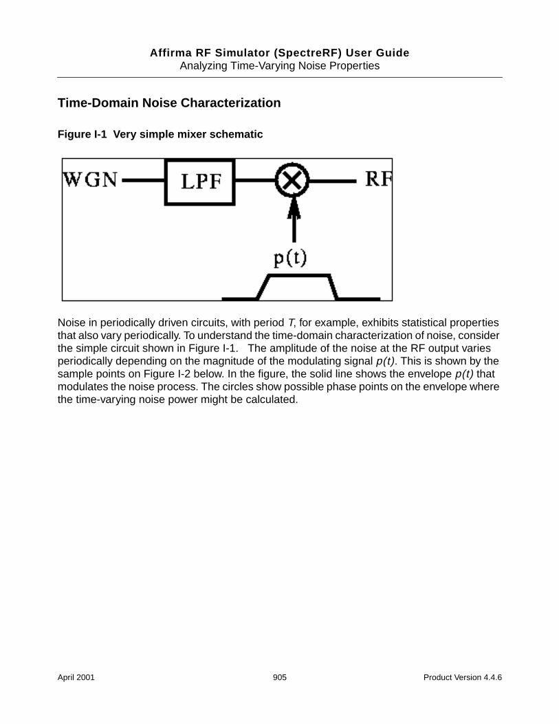
Affirma RF Simulator (SpectreRF) User GuideAnalyzing Time-Varying Noise Properties
Time-Domain Noise Characterization
Figure I-1 Very simple mixer schematic
Noise in periodically driven circuits, with period T, for example, exhibits statistical propertiesthat also vary periodically. To understand the time-domain characterization of noise, considerthe simple circuit shown in Figure I-1. The amplitude of the noise at the RF output variesperiodically depending on the magnitude of the modulating signal p(t). This is shown by thesample points on Figure I-2 below. In the figure, the solid line shows the envelope p(t) thatmodulates the noise process. The circles show possible phase points on the envelope wherethe time-varying noise power might be calculated.
April 2001 905 Product Version 4.4.6
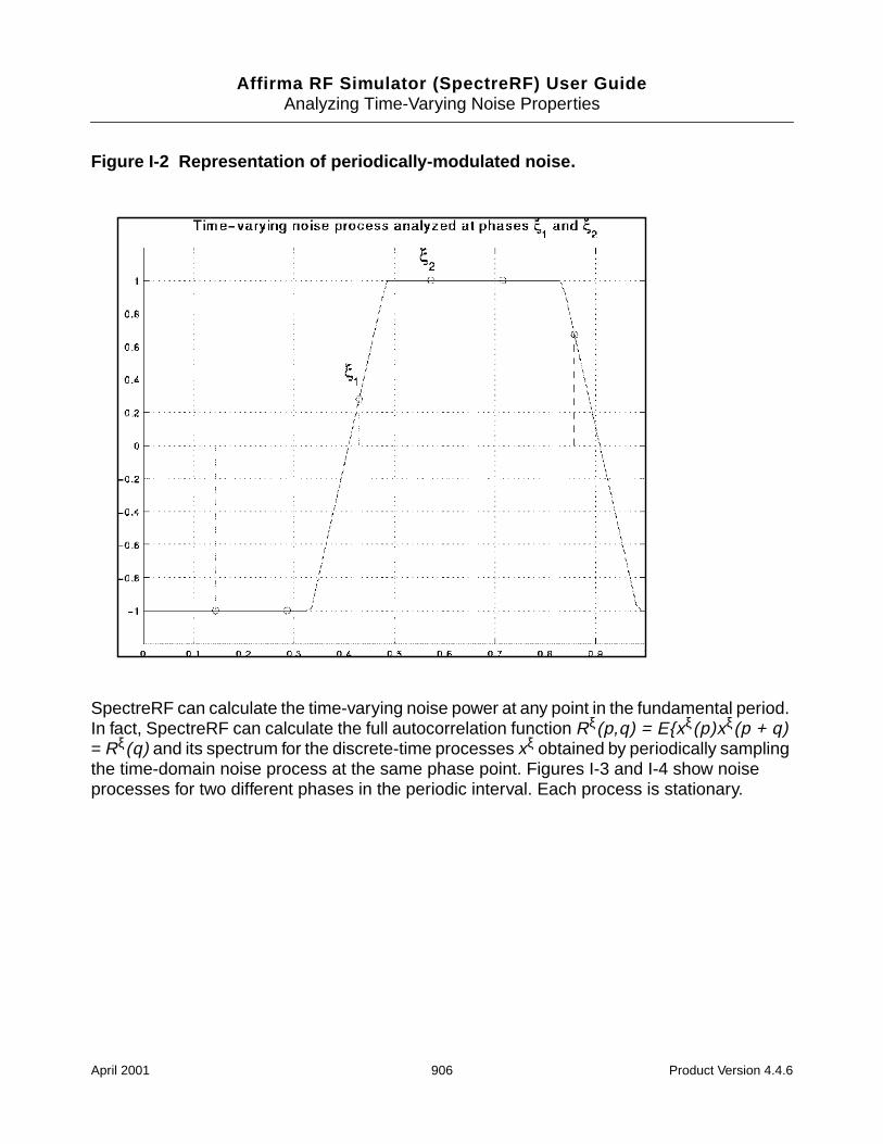
Affirma RF Simulator (SpectreRF) User GuideAnalyzing Time-Varying Noise Properties
Figure I-2 Representation of periodically-modulated noise.
SpectreRF can calculate the time-varying noise power at any point in the fundamental period.In fact, SpectreRF can calculate the full autocorrelation function Rξ(p,q) = Exξ(p)xξ(p + q)= Rξ(q) and its spectrum for the discrete-time processes xξ obtained by periodically samplingthe time-domain noise process at the same phase point. Figures I-3 and I-4 show noiseprocesses for two different phases in the periodic interval. Each process is stationary.
April 2001 906 Product Version 4.4.6
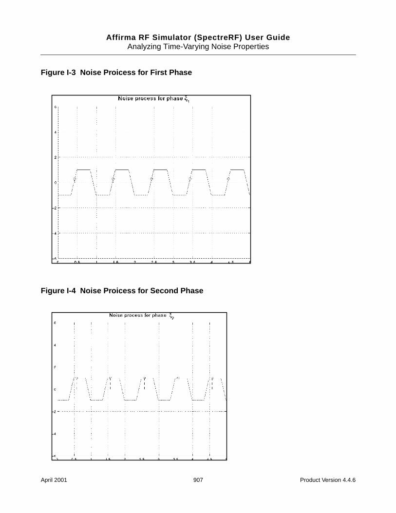
Affirma RF Simulator (SpectreRF) User GuideAnalyzing Time-Varying Noise Properties
Figure I-3 Noise Proicess for First Phase
Figure I-4 Noise Proicess for Second Phase
April 2001 907 Product Version 4.4.6
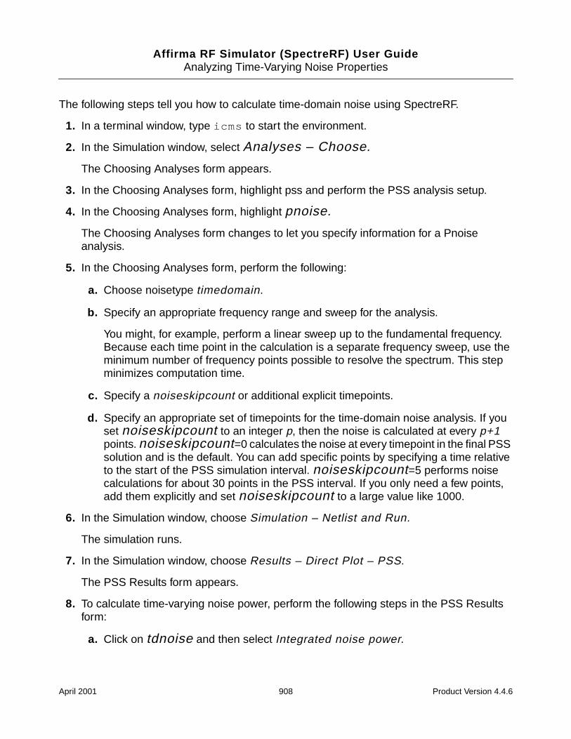
Affirma RF Simulator (SpectreRF) User GuideAnalyzing Time-Varying Noise Properties
The following steps tell you how to calculate time-domain noise using SpectreRF.
1. In a terminal window, type icms to start the environment.
2. In the Simulation window, select Analyses – Choose.
The Choosing Analyses form appears.
3. In the Choosing Analyses form, highlight pss and perform the PSS analysis setup.
4. In the Choosing Analyses form, highlight pnoise.
The Choosing Analyses form changes to let you specify information for a Pnoiseanalysis.
5. In the Choosing Analyses form, perform the following:
a. Choose noisetype timedomain.
b. Specify an appropriate frequency range and sweep for the analysis.
You might, for example, perform a linear sweep up to the fundamental frequency.Because each time point in the calculation is a separate frequency sweep, use theminimum number of frequency points possible to resolve the spectrum. This stepminimizes computation time.
c. Specify a noiseskipcount or additional explicit timepoints.
d. Specify an appropriate set of timepoints for the time-domain noise analysis. If youset noiseskipcount to an integer p, then the noise is calculated at every p+1points. noiseskipcount=0 calculates the noise at every timepoint in the final PSSsolution and is the default. You can add specific points by specifying a time relativeto the start of the PSS simulation interval. noiseskipcount=5 performs noisecalculations for about 30 points in the PSS interval. If you only need a few points,add them explicitly and set noiseskipcount to a large value like 1000.
6. In the Simulation window, choose Simulation – Netlist and Run.
The simulation runs.
7. In the Simulation window, choose Results – Direct Plot – PSS.
The PSS Results form appears.
8. To calculate time-varying noise power, perform the following steps in the PSS Resultsform:
a. Click on tdnoise and then select Integrated noise power.
April 2001 908 Product Version 4.4.6
Affirma RF Simulator (SpectreRF) User GuideAnalyzing Time-Varying Noise Properties
b. Type 0 as the start frequency and the PSS fundamental frequency as the stopperiod.
For example, type 1G if the PSS period is 1ns.
A periodic waveform appears that represents the expected noise power at each point inthe fundamental period.
9. To display the spectrum of the sampled processes, perform the following steps in thePSS Results form:
a. Highlight Output Noise.
b. Highlight Spectrum for the type of sweep.
c. Clicking on Plot.
A set of curves appears, one for each sample phase in the fundamental period.
10. To calculate the autocorrelation function for one of the sampled processes, perform thefollowing steps:
a. Display the spectrum using instructions from the previous step.
b. In the Simulation window, choose Tools – Calculator.
The calculator appears.
c. Click on wave in the calculator and the select the appropriate frequency-domainspectrum.
One of the sample waveforms is brought into the calculator
d. Choose DFT from the list of special functions in the calculator. Then set 0 as theFrom and the PSS fundamental as the To value.
e. Choose an appropriate window (e.g., Cosine2) and number of samples (around thenumber of frequency points in the interval[0,1/T]),
f. Apply the DFT and plot the results.
Harmonic q of the DFT results gives the value of the discrete autocorrelation for thissample phase, R(q).
Note: Be sure the noise is in the correct units of power (e.g., V2/Hz, not V/square rootof Hz) before performing the DFT to obtain the autocorrelation.
April 2001 909 Product Version 4.4.6
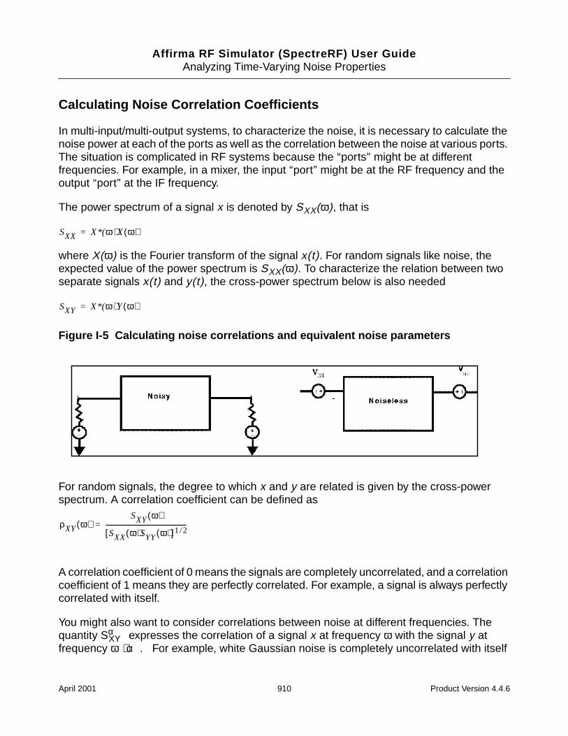
Affirma RF Simulator (SpectreRF) User GuideAnalyzing Time-Varying Noise Properties
Calculating Noise Correlation Coefficients
In multi-input/multi-output systems, to characterize the noise, it is necessary to calculate thenoise power at each of the ports as well as the correlation between the noise at various ports.The situation is complicated in RF systems because the ‘‘ports’’ might be at differentfrequencies. For example, in a mixer, the input ‘‘port’’ might be at the RF frequency and theoutput ‘‘port’’ at the IF frequency.
The power spectrum of a signal x is denoted by SXX(ω), that is
where X(ω) is the Fourier transform of the signal x(t). For random signals like noise, theexpected value of the power spectrum is SXX(ω). To characterize the relation between twoseparate signals x(t) and y(t), the cross-power spectrum below is also needed
Figure I-5 Calculating noise correlations and equivalent noise parameters
For random signals, the degree to which x and y are related is given by the cross-powerspectrum. A correlation coefficient can be defined as
A correlation coefficient of 0 means the signals are completely uncorrelated, and a correlationcoefficient of 1 means they are perfectly correlated. For example, a signal is always perfectlycorrelated with itself.
You might also want to consider correlations between noise at different frequencies. Thequantity Sα
XY expresses the correlation of a signal x at frequency ω with the signal y atfrequency ω + α. For example, white Gaussian noise is completely uncorrelated with itself
SXX X*(ω )X ω( )=
SXY X*(ω )Y ω( )=
ρXY ω( )SXY ω( )
SXX ω( )SYY ω( )[ ]1 2/----------------------------------------------------=
April 2001 910 Product Version 4.4.6
Affirma RF Simulator (SpectreRF) User GuideAnalyzing Time-Varying Noise Properties
for α ≠ 0. Noise in an RF system generally has Sα (ω) non-zero when α is a multiple of thefundamental frequency, such as for the LO frequency in a mixer.
Once the noise properties of a circuit are measured, these properties can be represented asa noiseless multiport with equivalent noise sources. For example, in Figure 3, the noisevoltage appearing at the excitation ports is first measured. Then the noise properties of thecircuit can be expressed as two equivalent frequency-dependent noise voltages VN1 andVN2, and a (complex) correlation coefficient ρ12.
The following steps describe how to calculate noise correlation parameters for a two-portcircuit.
1. In a terminal window, type icms to start the environment.
2. In the Simulation window, select Analyses – Choose.
The Choosing Analyses form appears.
3. In the Choosing Analyses form, highlight pss and set up the PSS analysis.
4. In the Choosing Analyses form, highlight pnoise.
The Choosing Analyses form changes to let you specify information for a Pnoiseanalysis.
5. In the Choosing Analyses form, perform the following:
a. Choose correlations for the noisetype.
b. Choose the first output of the circuit.
This can be a port or voltage if you want to calculate noise parameters starting inthe impedance representation. It can be a current if you want to use the admittancerepresentation. For example, in a mixer, you might choose the IF output here.
c. Choose an appropriate frequency range and sweep for the analysis.
For example, for the mixer you might want to sweep 100MHz around the IF output.Choose an appropriate set of ‘‘cycles’’ to use for the analysis. In a mixer, you mightset maxcycles=1 or add cycle ‘‘1’’ if you select the IF as output. This specificationcalculates noise correlations between the IF output at frequency ω and the noise atthe RF input frequency ω + ω0, where ω0 is the LO frequency.
6. In the Simulation window, choose Simulation – Netlist and Run.
The simulation runs.
7. To display the results, perform the following steps:
April 2001 911 Product Version 4.4.6
Affirma RF Simulator (SpectreRF) User GuideAnalyzing Time-Varying Noise Properties
a. In the Simulation window, choose Tools – Results Browser.
The Results Browser appears.
b. In the Results Browser, choose the pnoise analysis and the appropriate cycle ofinterest. (Correlations of noise at different frequencies appear as different‘‘harmonics’’ in the browser.)
A list of nodes and sources appears.
The correlation between the noise at the output you specify in the Simulationwindow and the noise induced at each of the nodes or sources has been calculated.You can plot it directly or further process it in the calculator.
To analyze the correlations with noise at a differential input/output, subtract thecross-power spectra appearing on the two nodes.
Note: Results of the noise correlations analysis are in units of power (such as V2/Hz).and the cross-power spectra are usually complex.
April 2001 912 Product Version 4.4.6
Affirma RF Simulator (SpectreRF) User Guide
JUsing Tabulated S-parameters
Models of many passive components commonly used in RF design are only available astables of S-parameter data. Any linear, time-invariant circuit network or component can becompletely characterized by specifying its S-parameter network at each frequency of interest.The “Using the nport Component ”section tells how to use S-parameter tables in RF analyses.
SpectreRF uses time-domain shooting methods to achieve excellent performance on large,highly nonlinear circuits. Consequently, using S-parameter data in SpectreRF is not asstraightforward as it is with frequency-domain simulators such as those based on harmonicbalance. Before performing an RF simulation such as PSS analysis, you must first convertthe frequency-domain S-parameters into an equivalent time-domain model. This conversionmight be time-consuming for large, complicated data sets. However, the nport component letsyou avoid performing the conversion process more than once. The procedure is describedlater in this paper.
There are three potential difficulties in converting to a time-domain model.
First, not every set of frequency domain data has a valid time-domain description. Time-domain models must be stable and causal, and you cannot generate a time-domain modelfor frequency-domain data that lacks these properties.
Secondly, to convert the s-parameter data into a time-domain description, the frequenciesbetween the tabulated points must be interpolated. This is true because the time-domaindescription of a frequency-domain model depends on every frequency, not just the ones givenat the tabulated points. A special, robust, high-order, rational interpolation algorithm performsthe interpolation. The rational interpolation process introduces some error into the final modeldescription. See the “Controlling Model Accuracy” section to understand and control thiserror. This section also tells you how to deal with data that contains noise that may corruptthe rational interpolation process.
Finally, any algorithm that converts S-parameters so they can be used in a time-domainsimulator must extrapolate the data outside the range of tabulated frequencies. By definition,some frequencies are not included in a tabular data file. In addition, extrapolation mightintroduce nonphysical effects into the model, particularly when the S-parameter data is onlygiven over a very narrow frequency range. The “Troubleshooting“ section tells you how to
April 2001 913 Product Version 4.4.6
Affirma RF Simulator (SpectreRF) User GuideUsing Tabulated S-parameters
diagnose and solve any problems. It also tells how to interpret the warning messages thatSpectreRF produces when a non-physical extrapolation might be occurring.
Using the nport component
You read S-parameter data into using the nport component. Follow these steps to prepare annport component for use in SpectreRF simulations.
1. Place the appropriate component from analogLib, such as n2port for a two-port S-parameter description, in the schematic.
2. Select the nport component and then edit the object properties.
3. In the first field of the Edit Object Properties form ("S-parameter data file"), type the nameof the file that contains the tabulated S-parameter data, such as sparam1.dat. As of the4.4.5 release, S-parameter files must be in the "Spectre" format. If your S-parameter datais in another industry standard format, you must use the sptr tool to convert the data toa format that Spectre can read.
4. Set the interpolation method to rational so you can use SpectreRF analyses such as PSSand PNoise. If you only plan to use non-RF analyses such as TRAN, DC, and SP, youcan select spline instead.
5. [Optional] Specify a path for a "ROM data file." This must be an absolute pathname, forexample, /usr/mydir/sparamtorom. Once SpectreRF converts the S-parameter data to atime-domain description, this file stores the time-domain model. Storing the modelensures that interpolation and conversion need not be repeated. See the “Model Reuse”section on page -918 for further details on this file. Be sure this file is distinct from theS-parameter data file.
6. [Optional] If you know the form of your data, the amount of noise in the data, or theaccuracy you require from the S-parameter interpolation, fill in the relerr, abserr orratorder fields as described in the “Controlling Model Accuracy” section..
7. Apply the changes to the nport component and run the simulation.
Controlling Model Accuracy
The nport component has three parameters to control the accuracy of the rationalinterpolation process, relerr, abserr, and ratorder. You can use these parameters to tradeaccuracy for model size. Usually, the more stringent the accuracy requirement, the higher themodel order. Higher-order models require longer simulation time. Spectre can automatically
April 2001 914 Product Version 4.4.6
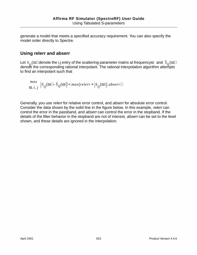
Affirma RF Simulator (SpectreRF) User GuideUsing Tabulated S-parameters
generate a model that meets a specified accuracy requirement. You can also specify themodel order directly to Spectre.
Using relerr and abserr
Let denote the i,j entry of the scattering parameter matrix at frequency anddenote the corresponding rational interpolant. The rational interpolation algorithm attemptsto find an interpolant such that
Generally, you use relerr for relative error control, and abserr for absolute error control.Consider the data shown by the solid line in the figure below. In this example, relerr cancontrol the error in the passband, and abserr can control the error in the stopband. If thedetails of the filter behavior in the stopband are not of interest, abserr can be set to the levelshown, and these details are ignored in the interpolation.
Sij ω( ) ω Sij ω( )
max
ω i j, ,Sij ω( ) Sij ω( )– max relerr Sij ω( )× abserr,( )<
April 2001 915 Product Version 4.4.6
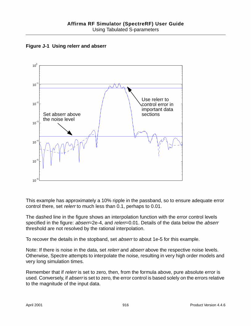
Affirma RF Simulator (SpectreRF) User GuideUsing Tabulated S-parameters
Figure J-1 Using relerr and abserr
This example has approximately a 10% ripple in the passband, so to ensure adequate errorcontrol there, set relerr to much less than 0.1, perhaps to 0.01.
The dashed line in the figure shows an interpolation function with the error control levelsspecified in the figure: abserr=2e-4, and relerr=0.01. Details of the data below the abserrthreshold are not resolved by the rational interpolation.
To recover the details in the stopband, set abserr to about 1e-5 for this example.
Note: If there is noise in the data, set relerr and abserr above the respective noise levels.Otherwise, Spectre attempts to interpolate the noise, resulting in very high order models andvery long simulation times.
Remember that if relerr is set to zero, then, from the formula above, pure absolute error isused. Conversely, if abserr is set to zero, the error control is based solely on the errors relativeto the magnitude of the input data.
10−6
10−5
10−4
10−3
10−2
10−1
100
Set abserr abovethe noise level
Use relerr tocontrol error inimportant datasections
April 2001 916 Product Version 4.4.6
Affirma RF Simulator (SpectreRF) User GuideUsing Tabulated S-parameters
Using the ratorder parameter
It is usually a good idea to specify only the accuracy parameters relerr and abserr, and letSpectre automatically select the order of the rational approximation. However, if you havespecial information about your data set, you can direct Spectre to use a specific order ofapproximation in the rational interpolation. For example, if you know that your tabulated S-parameter data represents a sixth-order filter, you might instruct spectre to use a seventh oreighth order fit. The slightly higher order gives Spectre flexibility to adjust for any noise or non-ideal behavior in the data.
When you specify the ratorder parameter, relerr and abserr are used to warn you if the orderyou selected is not sufficient to meet the accuracy requirements. Otherwise, the parametersare not used.
Troubleshooting
Some data sets can cause difficulty for the rational interpolation process. Types of data toavoid are
1. Data specified only over a very narrow frequency range.
Extrapolation of the data outside this range, needed for time-domain simulation, mightbe difficult and is always risky.
2. Very noisy data.
Such data might lead to large, unreliable time-domain models.
3. Data on a very sparse frequency grid.
Accurate interpolation of such data might be impossible.
4. Data with long ideal delays.
5. Data representing idealized lossless elements, such as lossless transmission lines.
Assessing the quality of the rational interpolation
If you suspect a problem with the rational interpolation process, you can investigate it usingthe sp analysis with the following steps:
Construct a test schematic consisting of an nport component with interpolation set torational, as discussed in the “Using the nport Component” section.
Next add the appropriate number of port components to the schematic.
April 2001 917 Product Version 4.4.6
Affirma RF Simulator (SpectreRF) User GuideUsing Tabulated S-parameters
Perform an sp analysis on the nport component and look for anomalies.
Large swings in interpolated values and S-parameter magnitudes greater than one suggesta problem. Large changes in the interpolant result from an inaccurate fit, and S-parametervalues greater than one result from a non-passive (energy-generating) model that mightcreate unstable time-domain solutions. Be particularly critical of anomalies near zerofrequency (DC).
If the anomalous behavior occurs inside the frequency range given in the S-parameter datafile, it usually indicates an inaccurate rational interpolation. Be sure all of the conditions givenabove are met. Try decreasing relerr or abserr or both, or specifying a higher-orderinterpolation with the ratorder parameter. Remember that measured data can contain finedetails that might require a higher order than you might expect from a casual inspection of thedata.
If the anomalous behavior occurs outside the tabulated frequency range, try changing theabserr, relerr, or ratorder parameters. Sometimes anomalies can be removed by using a moreaccurate fit. However, there are limits to the ability to extrapolate outside the frequencyinterval you specify. You might need to specify additional data points to fix the problem.
Model Reuse
The ROM data file feature of the nport lets you use the same S-parameter componentdescription across many designs, but only perform the conversion to a time-domain modelonce.
For a given S-parameter data set, after you have specified a location for the ROM data file,and Spectre performs the conversion to a time-domain model and writes the model file, youcan reuse the model file in future simulations. To reuse the model, you enter its name as the"ROM data file" in the new design. At this point, you no longer must specify a raw S-parameterdata file.
If you accidently specify both an S-parameter data file and a ROM data file, SpectreRF reusesthe model in the ROM data file if the two files are consistent. Otherwise, a new model isgenerated from the raw tabulated S-parameter data, and the ROM data file overwritten witha new model. This feature lets you specify both the ROM data file and the S-parameter datafile in a design when you first place the nport component. SpectreRF then automaticallygenerates the time-domain model for the first simulation and reuses it for all subsequentsimulations without needing to change the nport component parameters.
If you require a more accurate rational interpolation, then you must regenerate the model inthe ROM data file by changing the relerr, abserr or ratorder fields as described in the“Controlling Model Accuracy” section.
April 2001 918 Product Version 4.4.6
Affirma RF Simulator (SpectreRF) User GuideUsing Tabulated S-parameters
References
To learn technical details about how SpectreRF converts S-parameter data to a time-domaindescription, see the article "Robust rational function approximation algorithm for modelgeneration," by C. P. Coelho, J. R. Phillips, and L. M. Silveira. This article appeared in theproceedings of the 36th Design Automation Conference, New Orleans, LA, June 1999.
April 2001 919 Product Version 4.4.6
Affirma RF Simulator (SpectreRF) User Guide
KUsing the Calculator IPN Functions forRF Simulations
This appendix describes how to
Use the IPN functions in the Analog Design Environment Waveform Calculator.
Use the IPN functions with scalar inputs.
This appendix is designed for users of SpectreRF in the Affirma Analog Design Environmentand assumes that users are familiar with SpectreRF PSS, PAC, and Swept PSS analyses.
How to Use the ipn and ipnVRI Functions
This example uses the ne600 schematic from the rfExamples library. As you follow theexample, you combine a swept PSS analysis with a PAC analysis to produce data for an IP3plot. Then you will plot IP3 using the ipn and ipnVRI functions in the Calculator and comparethe results.
Setting Up
1. Start icms.
2. Copy the ne600 schematic from rfExamples to your local library (so you will have editpermissions on the schematic).
3. Open the ne600 schematic for edit.
4. From the schematic banner, Select Tools — Analog Environment . This opens theAnalog Circuit Design Simulation environment.
5. Open the Setup — Simulator/Directory/Host form and choose spectre as thesimulator and set Host Mode to local .
6. In the Model Library Setup form (Setup — Model libraries) , set the model library to
April 2001 920 Product Version 4.4.6
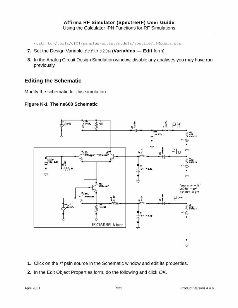
Affirma RF Simulator (SpectreRF) User GuideUsing the Calculator IPN Functions for RF Simulations
<path_to>/tools/dfII/samples/artist/models/spectre/rfModels.scs
7. Set the Design Variable frf to 920M (Variables — Edit form).
8. In the Analog Circuit Design Simulation window, disable any analyses you may have runpreviously.
Editing the Schematic
Modify the schematic for this simulation.
Figure K-1 The ne600 Schematic
1. Click on the rf psin source in the Schematic window and edit its properties.
2. In the Edit Object Properties form, do the following and click OK.
April 2001 921 Product Version 4.4.6
Affirma RF Simulator (SpectreRF) User GuideUsing the Calculator IPN Functions for RF Simulations
a. Type sine for Source type.
b. Type frf for Frequency.
c. Type prf in the Amplitude (dBm) and PAC magnitude (dBm) fields.
Be sure the Amplitude, Amplitude 2 (magnitude and dBm), and Frequency 2fields are empty. This simulation uses dBm values rather than magnitude.
3. Click on the lo psin source and edit its properties. Verify that the sourceType is set tosine .
4. In the schematic, select Design — Check and Save .
Setting Up the Analysis
1. In the Choosing Analyses form (Analyses — Choose ), select pss for the analysis.
2. In the Fundamental Tones list box, do the following and click OK.
a. select the Auto Calculate button.
b. The value 40M is specified as the Beat Frequency.
The PAC analysis is responsible for the two tones, and the PSS is now a singlesignal analysis. Consequently, the fundamental frequency is set to 40 MHz .
c. In the Output harmonics section, select Number of harmonics and enter 2 intothe field.
d. Click on conservative for the Accuracy Defaults (errpreset) setting.
e. Click on the Sweep button.
The form changes to let you specify data for the sweep.
In the Sweep option, select Variable .
Set Frequency Variable? to no.
Click on the Select Design Variable button.
Highlight prf in this form and click OK.
3. Select Start-Stop for the Sweep Range value, and then type −25 and 5 for the Startand Stop values, respectively. The sweep is skewed downward for a down converter.
4. Select Linear for the Sweep Type, and specify Step size = 5.
April 2001 922 Product Version 4.4.6
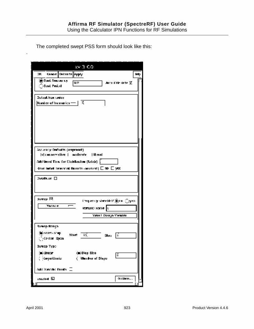
Affirma RF Simulator (SpectreRF) User GuideUsing the Calculator IPN Functions for RF Simulations
The completed swept PSS form should look like this:.
April 2001 923 Product Version 4.4.6
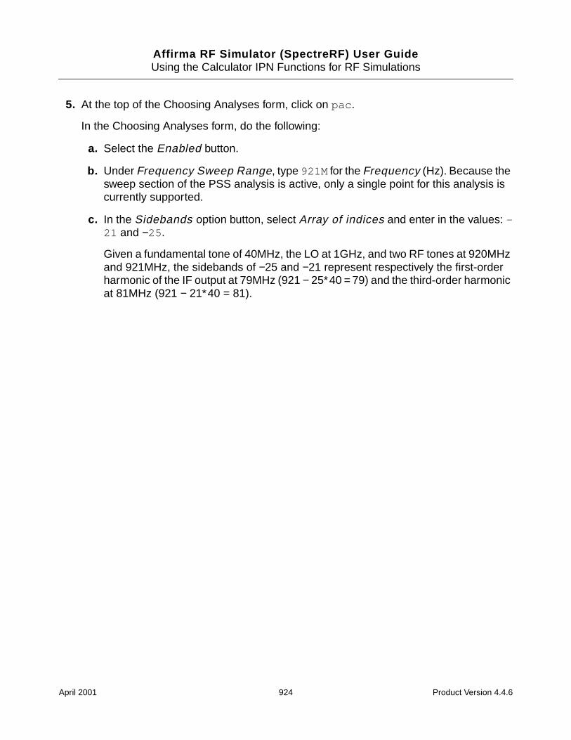
Affirma RF Simulator (SpectreRF) User GuideUsing the Calculator IPN Functions for RF Simulations
5. At the top of the Choosing Analyses form, click on pac .
In the Choosing Analyses form, do the following:
a. Select the Enabled button.
b. Under Frequency Sweep Range, type 921M for the Frequency (Hz). Because thesweep section of the PSS analysis is active, only a single point for this analysis iscurrently supported.
c. In the Sidebands option button, select Array of indices and enter in the values: -21 and −25 .
Given a fundamental tone of 40MHz, the LO at 1GHz, and two RF tones at 920MHzand 921MHz, the sidebands of −25 and −21 represent respectively the first-orderharmonic of the IF output at 79MHz (921 − 25∗40 = 79) and the third-order harmonicat 81MHz (921 − 21∗40 = 81).
April 2001 924 Product Version 4.4.6
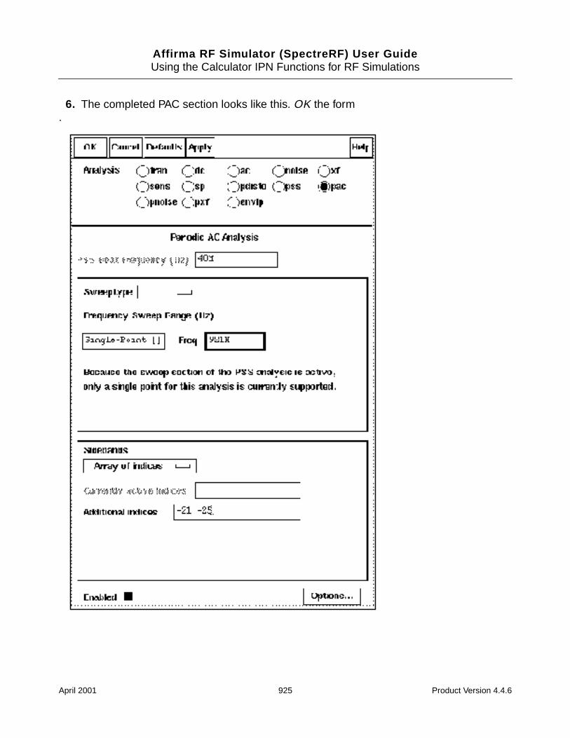
Affirma RF Simulator (SpectreRF) User GuideUsing the Calculator IPN Functions for RF Simulations
6. The completed PAC section looks like this. OK the form.
April 2001 925 Product Version 4.4.6
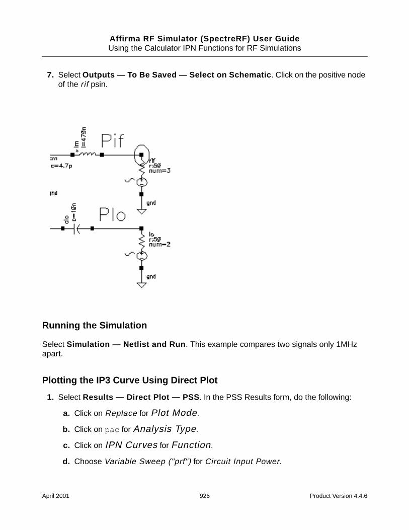
Affirma RF Simulator (SpectreRF) User GuideUsing the Calculator IPN Functions for RF Simulations
7. Select Outputs — To Be Saved — Select on Schematic . Click on the positive nodeof the rif psin.
Running the Simulation
Select Simulation — Netlist and Run . This example compares two signals only 1MHzapart.
Plotting the IP3 Curve Using Direct Plot
1. Select Results — Direct Plot — PSS . In the PSS Results form, do the following:
a. Click on Replace for Plot Mode.
b. Click on pac for Analysis Type.
c. Click on IPN Curves for Function.
d. Choose Variable Sweep ("prf") for Circuit Input Power.
April 2001 926 Product Version 4.4.6

Affirma RF Simulator (SpectreRF) User GuideUsing the Calculator IPN Functions for RF Simulations
e. Type -15 for Extrapolation Point. This value is the intercept point for the idealamplification extrapolation.
f. Select Input Referred IP3 and Order 3rd.
g. Highlight -21 81M in the 3rd Order Sideband list box.
h. Highlight -25 79M in the 1st Order Sideband list box.
April 2001 927 Product Version 4.4.6
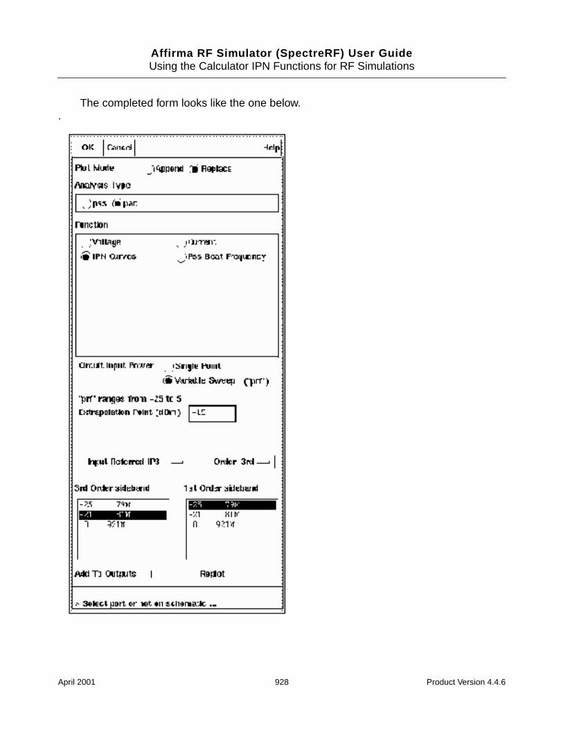
Affirma RF Simulator (SpectreRF) User GuideUsing the Calculator IPN Functions for RF Simulations
The completed form looks like the one below..
April 2001 928 Product Version 4.4.6
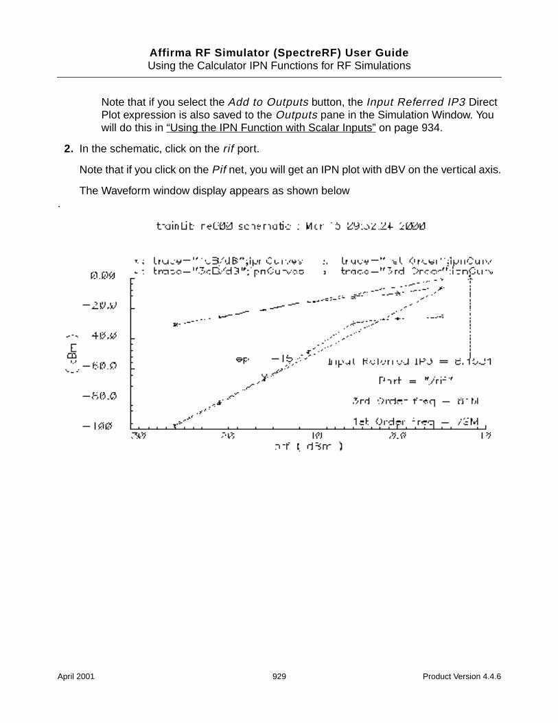
Affirma RF Simulator (SpectreRF) User GuideUsing the Calculator IPN Functions for RF Simulations
Note that if you select the Add to Outputs button, the Input Referred IP3 DirectPlot expression is also saved to the Outputs pane in the Simulation Window. Youwill do this in “Using the IPN Function with Scalar Inputs” on page 934.
2. In the schematic, click on the rif port.
Note that if you click on the Pif net, you will get an IPN plot with dBV on the vertical axis.
The Waveform window display appears as shown below.
April 2001 929 Product Version 4.4.6
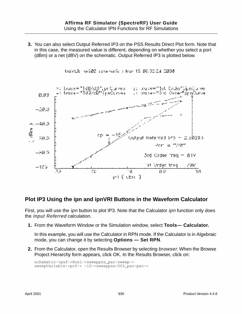
Affirma RF Simulator (SpectreRF) User GuideUsing the Calculator IPN Functions for RF Simulations
3. You can also select Output Referred IP3 on the PSS Results Direct Plot form. Note thatin this case, the measured value is different, depending on whether you select a port(dBm) or a net (dBV) on the schematic. Output Referred IP3 is plotted below.
Plot IP3 Using the ipn and ipnVRI Buttons in the Waveform Calculator
First, you will use the ipn button to plot IP3. Note that the Calculator ipn function only doesthe Input Referred calculation.
1. From the Waveform Window or the Simulation window, select Tools— Calculator.
In this example, you will use the Calculator in RPN mode. If the Calculator is in Algebraicmode, you can change it by selecting Options — Set RPN .
2. From the Calculator, open the Results Browser by selecting browser. When the BrowseProject Hierarchy form appears, click OK. In the Results Browser, click on:
schematic–>psf–>Run1–>sweeppss_pac-sweep–>sweepVariable–>prf–> –10–>sweeppss-003_pac-pac–>
April 2001 930 Product Version 4.4.6
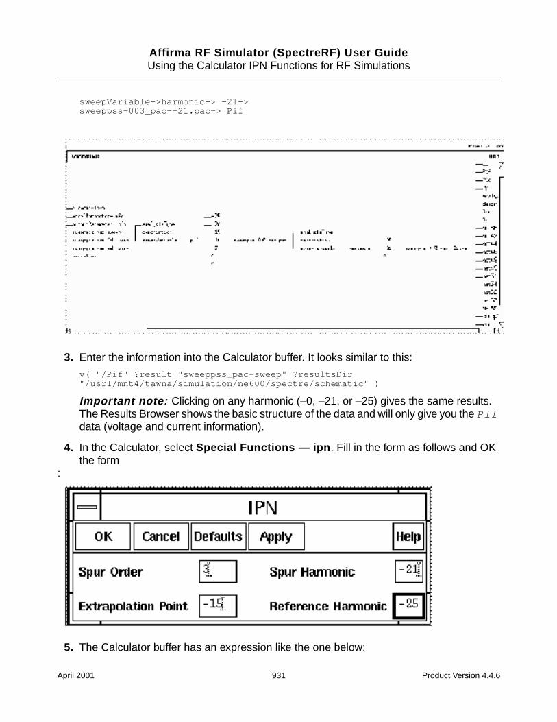
Affirma RF Simulator (SpectreRF) User GuideUsing the Calculator IPN Functions for RF Simulations
sweepVariable–>harmonic–> –21–>sweeppss-003_pac--21.pac–> Pif
3. Enter the information into the Calculator buffer. It looks similar to this:
v( "/Pif" ?result "sweeppss_pac-sweep" ?resultsDir"/usr1/mnt4/tawna/simulation/ne600/spectre/schematic" )
Important note: Clicking on any harmonic (–0, –21, or –25) gives the same results.The Results Browser shows the basic structure of the data and will only give you the Pifdata (voltage and current information).
4. In the Calculator, select Special Functions — ipn . Fill in the form as follows and OKthe form
:
5. The Calculator buffer has an expression like the one below:
April 2001 931 Product Version 4.4.6
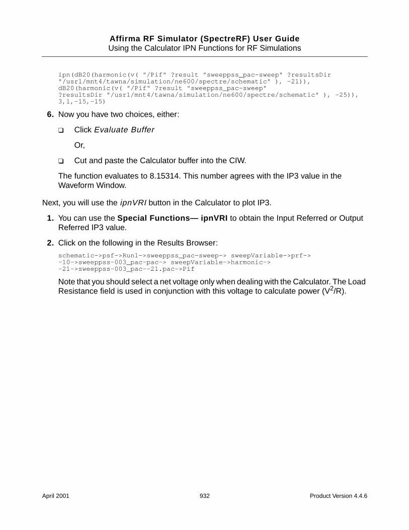
Affirma RF Simulator (SpectreRF) User GuideUsing the Calculator IPN Functions for RF Simulations
ipn(dB20(harmonic(v( "/Pif" ?result "sweeppss_pac-sweep" ?resultsDir"/usr1/mnt4/tawna/simulation/ne600/spectre/schematic" ), -21)),dB20(harmonic(v( "/Pif" ?result "sweeppss_pac-sweep"?resultsDir "/usr1/mnt4/tawna/simulation/ne600/spectre/schematic" ), -25)),3,1,-15,-15)
6. Now you have two choices, either:
Click Evaluate Buffer
Or,
Cut and paste the Calculator buffer into the CIW.
The function evaluates to 8.15314. This number agrees with the IP3 value in theWaveform Window.
Next, you will use the ipnVRI button in the Calculator to plot IP3.
1. You can use the Special Functions— ipnVRI to obtain the Input Referred or OutputReferred IP3 value.
2. Click on the following in the Results Browser:
schematic–>psf–>Run1–>sweeppss_pac-sweep–> sweepVariable–>prf–>–10–>sweeppss-003_pac-pac–> sweepVariable–>harmonic–>–21–>sweeppss-003_pac--21.pac–>Pif
Note that you should select a net voltage only when dealing with the Calculator. The LoadResistance field is used in conjunction with this voltage to calculate power (V2/R).
April 2001 932 Product Version 4.4.6
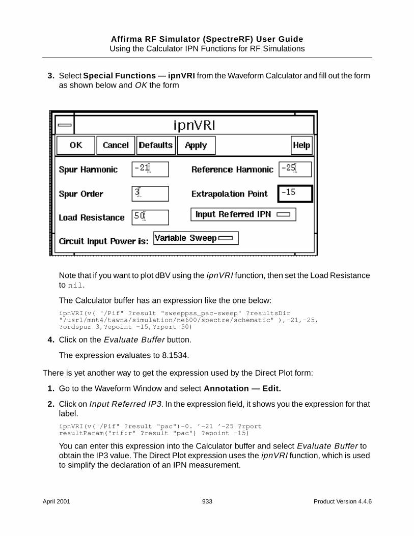
Affirma RF Simulator (SpectreRF) User GuideUsing the Calculator IPN Functions for RF Simulations
3. Select Special Functions — ipnVRI from the Waveform Calculator and fill out the formas shown below and OK the form
Note that if you want to plot dBV using the ipnVRI function, then set the Load Resistanceto nil .
The Calculator buffer has an expression like the one below:
ipnVRI(v( "/Pif" ?result "sweeppss_pac-sweep" ?resultsDir"/usr1/mnt4/tawna/simulation/ne600/spectre/schematic" ),-21,-25,?ordspur 3,?epoint -15,?rport 50)
4. Click on the Evaluate Buffer button.
The expression evaluates to 8.1534.
There is yet another way to get the expression used by the Direct Plot form:
1. Go to the Waveform Window and select Annotation — Edit.
2. Click on Input Referred IP3. In the expression field, it shows you the expression for thatlabel.
ipnVRI(v("/Pif" ?result "pac")-0. ’-21 ’-25 ?rportresultParam("rif:r" ?result "pac") ?epoint -15)
You can enter this expression into the Calculator buffer and select Evaluate Buffer toobtain the IP3 value. The Direct Plot expression uses the ipnVRI function, which is usedto simplify the declaration of an IPN measurement.
April 2001 933 Product Version 4.4.6
Affirma RF Simulator (SpectreRF) User GuideUsing the Calculator IPN Functions for RF Simulations
Using the IPN Function with Scalar Inputs
This example uses the ne600 schematic from the rfExamples library.
Two reasons to use the IPN function with scalar inputs (assuming region of operation is linear)are:
simulation is faster
IPN optimization is faster
When you use scalar inputs, always do a final IPN verification with a power sweep (non-scalarinputs), as outlined in the previous example.
Setting Up
Start icms and edit the schematic as described in the previous example. See “SettingUp” on page 920 for more information.
Setting Up the Analysis
1. In the Choosing Analyses form (Analyses — Choose ), select pss for the analysis.
The analysis will be set up similar to the previous example, except this time the Sweepbutton is disabled.
a. In the Fundamental Tones list box, select the Auto Calculate button
b. In the Output harmonics option button, select Number of harmonics = 2.
c. Click on conservative for the Accuracy Defaults (errpreset) setting.
April 2001 934 Product Version 4.4.6
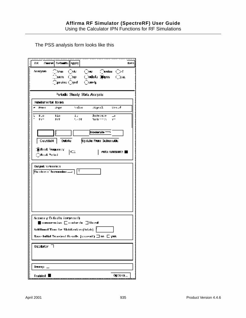
Affirma RF Simulator (SpectreRF) User GuideUsing the Calculator IPN Functions for RF Simulations
The PSS analysis form looks like this
April 2001 935 Product Version 4.4.6
Affirma RF Simulator (SpectreRF) User GuideUsing the Calculator IPN Functions for RF Simulations
2. At the top of the Choosing Analyses form, click on pac .
a. Set the Frequency Sweep Range to Single-Point, and freq to 921M.
b. In the Sidebands option, select Array of indices and type in the Additionalindices field: -21 and -25 .
c. Given a fundamental tone of 40MHz, the LO at 1GHz, and two RF tones at 920MHzand 921MHz, the sidebands of -25 and -21 represent respectively the first-orderharmonic of the IF output at 79MHz (921 - 25*40 = 79) and the third-order harmonicat 81MHz (921 - 21*40 = 81).
April 2001 936 Product Version 4.4.6
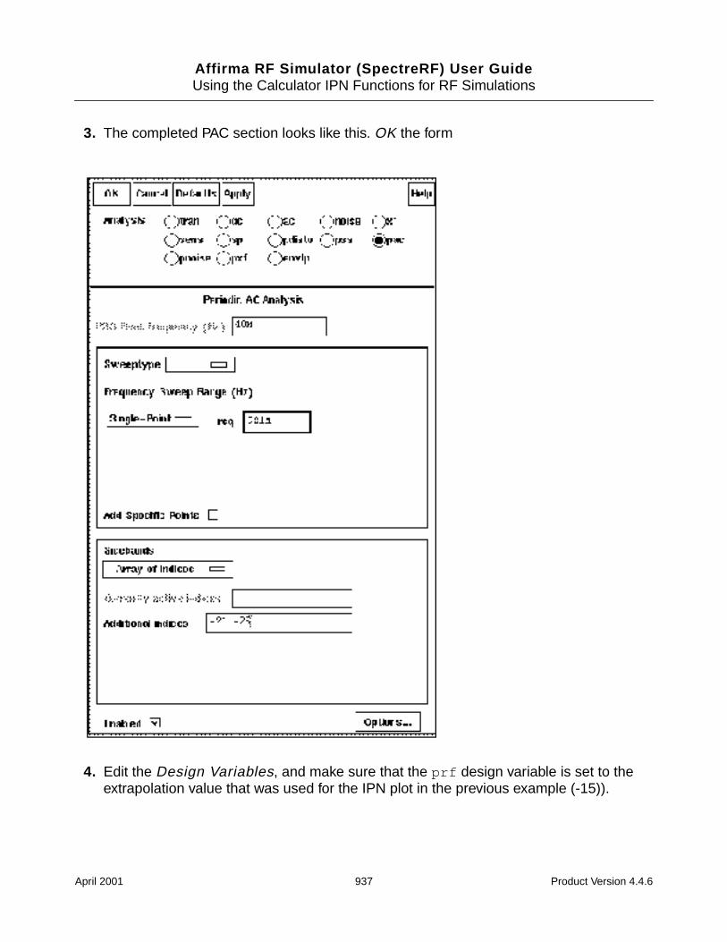
Affirma RF Simulator (SpectreRF) User GuideUsing the Calculator IPN Functions for RF Simulations
3. The completed PAC section looks like this. OK the form
4. Edit the Design Variables, and make sure that the prf design variable is set to theextrapolation value that was used for the IPN plot in the previous example (-15)).
April 2001 937 Product Version 4.4.6
Affirma RF Simulator (SpectreRF) User GuideUsing the Calculator IPN Functions for RF Simulations
Running Simulation
Select Simulation— Netlist and Run .
April 2001 938 Product Version 4.4.6
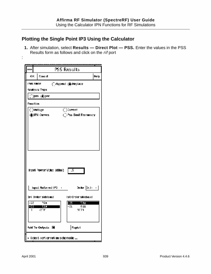
Affirma RF Simulator (SpectreRF) User GuideUsing the Calculator IPN Functions for RF Simulations
Plotting the Single Point IP3 Using the Calculator
1. After simulation, select Results — Direct Plot — PSS. Enter the values in the PSSResults form as follows and click on the rif port
:
April 2001 939 Product Version 4.4.6
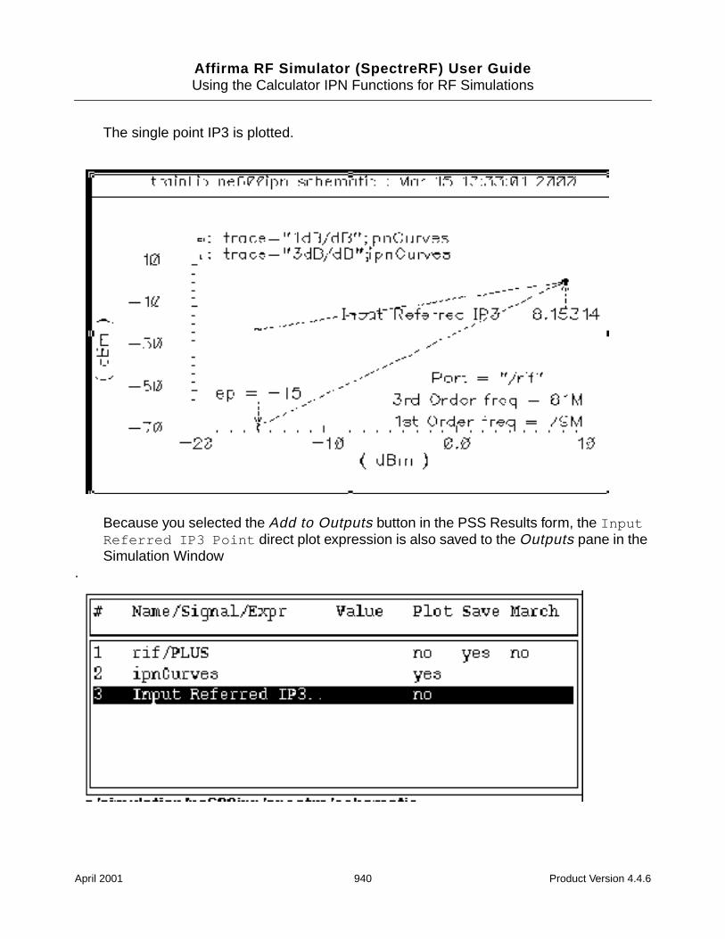
Affirma RF Simulator (SpectreRF) User GuideUsing the Calculator IPN Functions for RF Simulations
The single point IP3 is plotted.
Because you selected the Add to Outputs button in the PSS Results form, the InputReferred IP3 Point direct plot expression is also saved to the Outputs pane in theSimulation Window
.
April 2001 940 Product Version 4.4.6
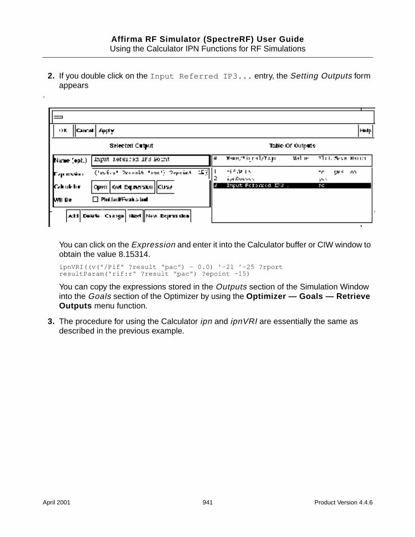
Affirma RF Simulator (SpectreRF) User GuideUsing the Calculator IPN Functions for RF Simulations
2. If you double click on the Input Referred IP3... entry, the Setting Outputs formappears
.
You can click on the Expression and enter it into the Calculator buffer or CIW window toobtain the value 8.15314.
ipnVRI((v("/Pif" ?result "pac") - 0.0) ’-21 ’-25 ?rportresultParam("rif:r" ?result "pac") ?epoint -15)
You can copy the expressions stored in the Outputs section of the Simulation Windowinto the Goals section of the Optimizer by using the Optimizer — Goals — RetrieveOutputs menu function.
3. The procedure for using the Calculator ipn and ipnVRI are essentially the same asdescribed in the previous example.
April 2001 941 Product Version 4.4.6
Affirma RF Simulator (SpectreRF) User Guide
LUsing PSP and Pnoise Analyses
Overview
This appendix describes how to calculate small-signal quantities such as noise, noise figure,periodic scattering parameters, and gain in periodically-driven circuits. The appendix explains
The concepts of periodic S-parameters,
The concepts of noise correlation parameters
The various definitions of noise figure and gain
The Spectre simulator provides four small-signal analyses for circuits with a DC operatingpoint: AC, XF, Noise and SP. The SpectreRF simulator also provides four small-signalanalyses for circuits with a a periodically time-varying operating point: PAC, PXF, Pnoise andPSP. Because the periodic small-signal analyses linearize the circuit about the time-varyingoperating point that is obtained using the PSS analysis, they can analyze frequencyconversion effects.
PAC analysis computes the small-signal response at all outputs to the small stimulus ofa single group of sources.
PXF analysis computes the transfer function from every source in the circuit to a singleoutput.
Pnoise analysis computes noise parameters such as noise figure as well as detailingnoise contributions by devices.
PSP analysis contains some of the capabilities of PAC, PXF, and Pnoise analyses. PSPanalysis can compute periodic scattering parameters that describe the small-signalrelations between several different ports in a circuit. It can also compute noiseparameters, such as noise correlation matrices, equivalent noise sources, and noisefigure.
April 2001 942 Product Version 4.4.6
Affirma RF Simulator (SpectreRF) User GuideUsing PSP and Pnoise Analyses
Periodic S-parameters
Linear Time-Invariant S-Parameters
Designers of microwave and RF circuits typically characterize the frequency-dependentbehavior of linear networks through sets of scattering or S-parameters. The notion ofscattering parameters is rooted in transmission line concepts where the scattering parametermatrix relates the magnitude and phase of incident and reflected waves.
Consider an arbitrary N-port linear time-invariant (LTI) network, such as the two-port shownin Figure 12-1 on page 944. Each port is driven by a source of reference impedance Zi , wherethe index i runs from 1 to N. For the remainder of this document we will assume a real valuedreference impedance, Ri, for each port. In terms of the port currents I i and voltages Vi , theincident and reflected quantities, ai and bi respectively, are defined for each port as
The frequency-dependent S-parameter matrix relates a and b by
These definitions are possible because for LTI systems, sources at a frequency ω generatesteady-state responses, and therefore outputs, at the same frequency.
ai
vi
2 Ri
-------------Ri2
--------- I i+=
bi
vi
2 Ri
-------------Ri2
---------I i–=
b ω( ) S ω( )a ω( )=
April 2001 943 Product Version 4.4.6
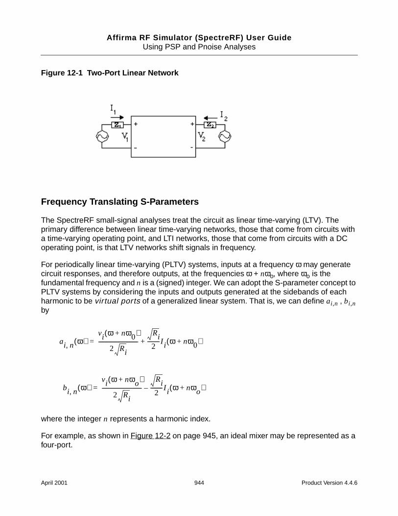
Affirma RF Simulator (SpectreRF) User GuideUsing PSP and Pnoise Analyses
Figure 12-1 Two-Port Linear Network
Frequency Translating S-Parameters
The SpectreRF small-signal analyses treat the circuit as linear time-varying (LTV). Theprimary difference between linear time-varying networks, those that come from circuits witha time-varying operating point, and LTI networks, those that come from circuits with a DCoperating point, is that LTV networks shift signals in frequency.
For periodically linear time-varying (PLTV) systems, inputs at a frequency ω may generatecircuit responses, and therefore outputs, at the frequencies ω + nωo, where ωo is thefundamental frequency and n is a (signed) integer. We can adopt the S-parameter concept toPLTV systems by considering the inputs and outputs generated at the sidebands of eachharmonic to be virtual ports of a generalized linear system. That is, we can define ai,n , bi,nby
where the integer n represents a harmonic index.
For example, as shown in Figure 12-2 on page 945, an ideal mixer may be represented as afour-port.
ai n, ω( )vi ω nω0+( )
2 Ri
------------------------------Ri2
---------I i ω nω0+( )+=
bi n, ω( )vi ω nωo+( )
2 Ri
------------------------------Ri2
--------- I i ω nωo+( )–=
April 2001 944 Product Version 4.4.6
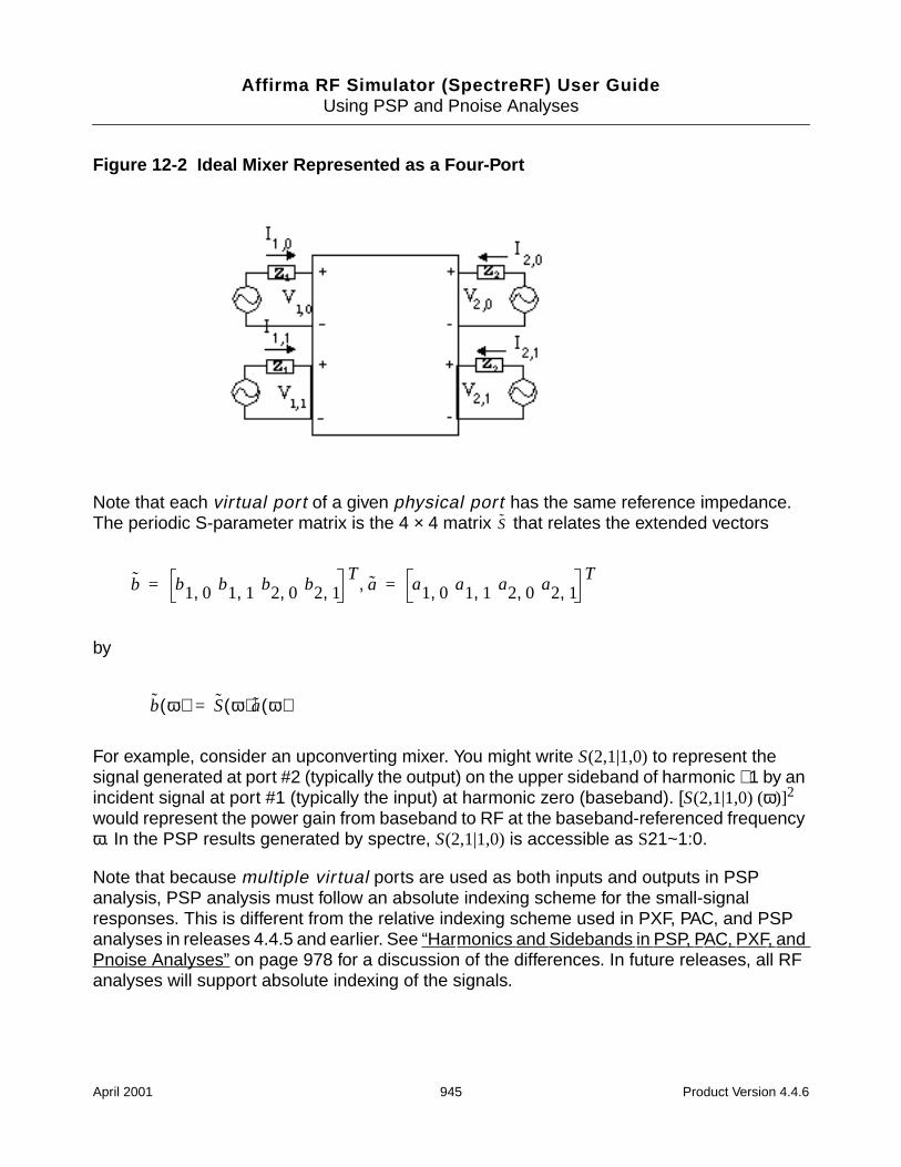
Affirma RF Simulator (SpectreRF) User GuideUsing PSP and Pnoise Analyses
Figure 12-2 Ideal Mixer Represented as a Four-Port
Note that each virtual port of a given physical port has the same reference impedance.The periodic S-parameter matrix is the 4 × 4 matrix that relates the extended vectors
by
For example, consider an upconverting mixer. You might write S(2,1|1,0) to represent thesignal generated at port #2 (typically the output) on the upper sideband of harmonic +1 by anincident signal at port #1 (typically the input) at harmonic zero (baseband). [S(2,1|1,0) (ω)]2
would represent the power gain from baseband to RF at the baseband-referenced frequencyω. In the PSP results generated by spectre, S(2,1|1,0) is accessible as S21~1:0.
Note that because multiple virtual ports are used as both inputs and outputs in PSPanalysis, PSP analysis must follow an absolute indexing scheme for the small-signalresponses. This is different from the relative indexing scheme used in PXF, PAC, and PSPanalyses in releases 4.4.5 and earlier. See “Harmonics and Sidebands in PSP, PAC, PXF, andPnoise Analyses” on page 978 for a discussion of the differences. In future releases, all RFanalyses will support absolute indexing of the signals.
S
b b1 0, b1 1, b2 0, b2 1,T
a, a1 0, a1 1, a2 0, a2 1,T
= =
b ω( ) S ω( )a ω( )=
April 2001 945 Product Version 4.4.6
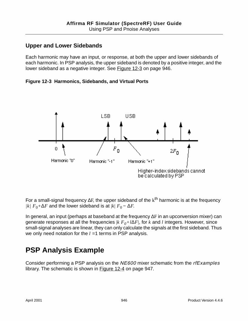
Affirma RF Simulator (SpectreRF) User GuideUsing PSP and Pnoise Analyses
Upper and Lower Sidebands
Each harmonic may have an input, or response, at both the upper and lower sidebands ofeach harmonic. In PSP analysis, the upper sideband is denoted by a positive integer, and thelower sideband as a negative integer. See Figure 12-3 on page 946.
Figure 12-3 Harmonics, Sidebands, and Virtual Ports
For a small-signal frequency ∆F, the upper sideband of the kth harmonic is at the frequency|k| F0+ ∆F and the lower sideband is at |k| F0 − ∆F.
In general, an input (perhaps at baseband at the frequency ∆F in an upconversion mixer) cangenerate responses at all the frequencies |k F0+l ∆F|, for k and l integers. However, sincesmall-signal analyses are linear, they can only calculate the signals at the first sideband. Thuswe only need notation for the l =1 terms in PSP analysis.
PSP Analysis Example
Consider performing a PSP analysis on the NE600 mixer schematic from the rfExampleslibrary. The schematic is shown in Figure 12-4 on page 947.
April 2001 946 Product Version 4.4.6
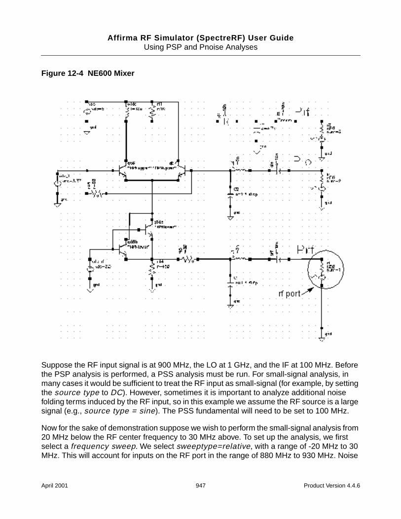
Affirma RF Simulator (SpectreRF) User GuideUsing PSP and Pnoise Analyses
Figure 12-4 NE600 Mixer
Suppose the RF input signal is at 900 MHz, the LO at 1 GHz, and the IF at 100 MHz. Beforethe PSP analysis is performed, a PSS analysis must be run. For small-signal analysis, inmany cases it would be sufficient to treat the RF input as small-signal (for example, by settingthe source type to DC). However, sometimes it is important to analyze additional noisefolding terms induced by the RF input, so in this example we assume the RF source is a largesignal (e.g., source type = sine). The PSS fundamental will need to be set to 100 MHz.
Now for the sake of demonstration suppose we wish to perform the small-signal analysis from20 MHz below the RF center frequency to 30 MHz above. To set up the analysis, we firstselect a frequency sweep. We select sweeptype=relative, with a range of -20 MHz to 30MHz. This will account for inputs on the RF port in the range of 880 MHz to 930 MHz. Noise
April 2001 947 Product Version 4.4.6
Affirma RF Simulator (SpectreRF) User GuideUsing PSP and Pnoise Analyses
parameters such as noise figure will be computed in a 50 MHz band around the frequencyspecified by the output harmonic.
Next we select the ports and harmonics. The input and output ports are selected from theschematic as always. Selecting the harmonics is somewhat trickier.
With the 1 GHz LO, small-signal inputs at around 900 MHz, or harmonics +/−9 of the PSSfundamental, will appear at around 100 MHz, or harmonics −/+1 of the fundamental. We mayselect harmonic 1 as the output harmonic and harmonic -9 as the input harmonic because asingle complex-exponential input, , input on the lower side of 900 MHz (harmonic -9) willappear as the upper sideband of harmonic 1 (around 100 MHz). -9 and 1 are separated by10 fundamental periods, which corresponds to the LO frequency of 1 GHz. Figure 12-5 onpage 949 conceptually illustrates this setup.
Once the simulation is complete, a limited set of data is accessible through direct plot, andthe full data set is accessible with the results browser. The default is to output all quantitiesversus the input frequency, which in this case would be a sweep from -920 MHz to -870 MHz,because the input harmonic is -9 and the sweep ran from -20 Mhz to 30 MHz. The freqaxisparameter on the options form may be used to change the axes that are output by Spectre.In 4.4.5 the freqaxis parameter and frequency sweep specifications are solely responsiblefor the data’s axis generation. Setting freqaxis=out in this example would produce an axisrunning from 80 Mhz to 130 Mhz.
eiωst
April 2001 948 Product Version 4.4.6
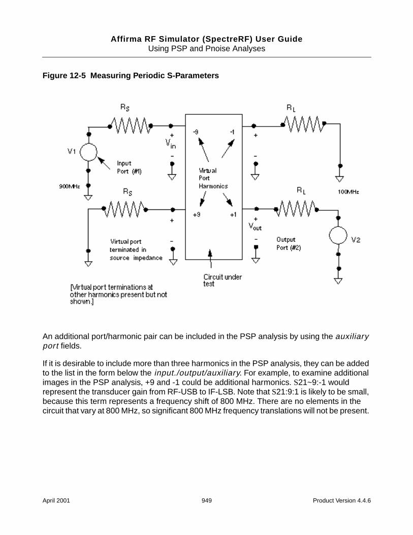
Affirma RF Simulator (SpectreRF) User GuideUsing PSP and Pnoise Analyses
Figure 12-5 Measuring Periodic S-Parameters
An additional port/harmonic pair can be included in the PSP analysis by using the auxiliaryport fields.
If it is desirable to include more than three harmonics in the PSP analysis, they can be addedto the list in the form below the input./output/auxiliary. For example, to examine additionalimages in the PSP analysis, +9 and -1 could be additional harmonics. S21~9:-1 wouldrepresent the transducer gain from RF-USB to IF-LSB. Note that S21:9:1 is likely to be small,because this term represents a frequency shift of 800 MHz. There are no elements in thecircuit that vary at 800 MHz, so significant 800 MHz frequency translations will not be present.
April 2001 949 Product Version 4.4.6
Affirma RF Simulator (SpectreRF) User GuideUsing PSP and Pnoise Analyses
Noise and Noise Parameters
Calculating Noise in Linear Time-Invariant (DC Bias) Circuits
The standard Noise analysis has two parts.
First, the circuit is analyzed without the noise sources present in order to find a DCoperating point.
Next, the circuit is linearized around that operating point and the noise sources areturned on.
The linearized circuit is used to compute a set of transfer functions that represent the gainfrom each noise source to the node pair or probe that is identified as the output for the Noiseanalysis. All noise generators present in the circuit are automatically included in the Noiseanalysis, as are the noise sources of the source and load.
Calculating Noise in Time-Varying (Periodic Bias) Circuits
Noise analysis in RF circuits, where the circuit operating point is time-varying, iscomputationally involved, but conceptually similar to Noise analysis for circuits with a DC bias.
Find the circuit operating point using the PSS analysis.
Linearize the circuit around that operating point.
Use the PXF analysis, based on the linearized circuit, to compute a set of transferfunctions that relate the noise sources to the noise at the circuit output.
The treatment of the sources and the transfer functions is more complicated for RF circuitsbecause of the time-varying operating point.
For noise sources that are bias dependent, such as shot noise sources, the time-varyingoperating point acts to modulate the noise sources. Active elements with a time-varying biaspoint can convert noise from one frequency to another, a process known as noise folding,regardless of the origin of the noise.
Because of these effects, noise generated in RF circuits usually has cyclostationaryproperties. Cyclostationary random processes are processes whose statistical properties areperiodically time-varying. In the frequency domain, a simple way to think of cyclostationarityis as frequency-correlation. For example, noise at the input of a mixer will appear on theoutput, but shifted in frequency. Thus the noise at the mixer output at a given frequency willbe correlated with noise at the mixer input at a frequency separated by the frequency of the
April 2001 950 Product Version 4.4.6
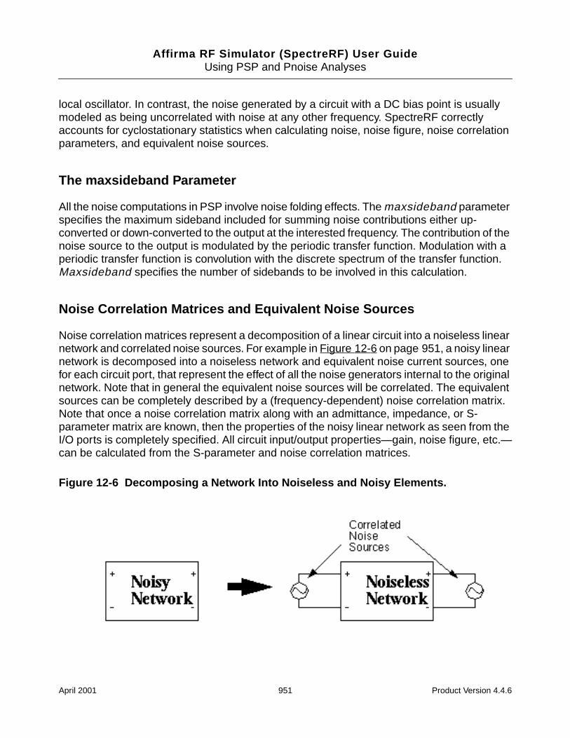
Affirma RF Simulator (SpectreRF) User GuideUsing PSP and Pnoise Analyses
local oscillator. In contrast, the noise generated by a circuit with a DC bias point is usuallymodeled as being uncorrelated with noise at any other frequency. SpectreRF correctlyaccounts for cyclostationary statistics when calculating noise, noise figure, noise correlationparameters, and equivalent noise sources.
The maxsideband Parameter
All the noise computations in PSP involve noise folding effects. The maxsideband parameterspecifies the maximum sideband included for summing noise contributions either up-converted or down-converted to the output at the interested frequency. The contribution of thenoise source to the output is modulated by the periodic transfer function. Modulation with aperiodic transfer function is convolution with the discrete spectrum of the transfer function.Maxsideband specifies the number of sidebands to be involved in this calculation.
Noise Correlation Matrices and Equivalent Noise Sources
Noise correlation matrices represent a decomposition of a linear circuit into a noiseless linearnetwork and correlated noise sources. For example in Figure 12-6 on page 951, a noisy linearnetwork is decomposed into a noiseless network and equivalent noise current sources, onefor each circuit port, that represent the effect of all the noise generators internal to the originalnetwork. Note that in general the equivalent noise sources will be correlated. The equivalentsources can be completely described by a (frequency-dependent) noise correlation matrix.Note that once a noise correlation matrix along with an admittance, impedance, or S-parameter matrix are known, then the properties of the noisy linear network as seen from theI/O ports is completely specified. All circuit input/output properties—gain, noise figure, etc.—can be calculated from the S-parameter and noise correlation matrices.
Figure 12-6 Decomposing a Network Into Noiseless and Noisy Elements.
April 2001 951 Product Version 4.4.6
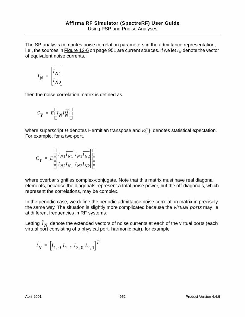
Affirma RF Simulator (SpectreRF) User GuideUsing PSP and Pnoise Analyses
The SP analysis computes noise correlation parameters in the admittance representation,i.e., the sources in Figure 12-6 on page 951 are current sources. If we let IN denote the vectorof equivalent noise currents.
then the noise correlation matrix is defined as
where superscript H denotes Hermitian transpose and E° denotes statistical expectation.For example, for a two-port,
where overbar signifies complex-conjugate. Note that this matrix must have real diagonalelements, because the diagonals represent a total noise power, but the off-diagonals, whichrepresent the correlations, may be complex.
In the periodic case, we define the periodic admittance noise correlation matrix in preciselythe same way. The situation is slightly more complicated because the virtual ports may lieat different frequencies in RF systems.
Letting denote the extended vectors of noise currents at each of the virtual ports (eachvirtual port consisting of a physical port. harmonic pair), for example
I N
I N1
I N2
=
CY E INI NH
=
CY EI N1I N1 I N1I N2
I N2I N1 I N2I N2
=
I N
I N˜ I 1 0, I 1 1, I 2 0, I 2 1,
T=
April 2001 952 Product Version 4.4.6
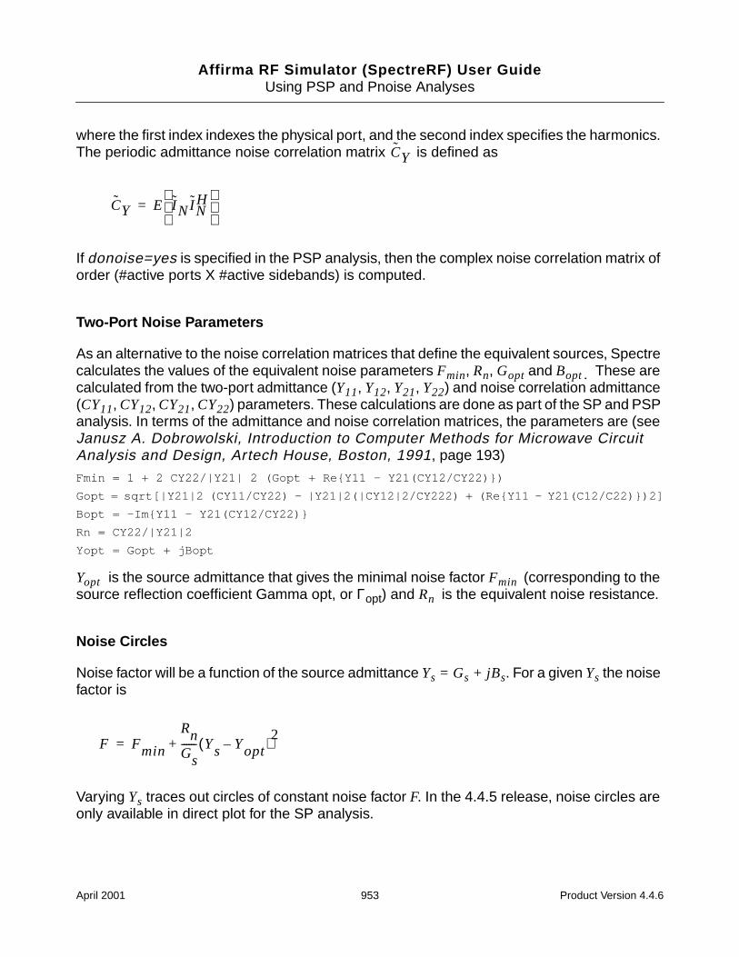
Affirma RF Simulator (SpectreRF) User GuideUsing PSP and Pnoise Analyses
where the first index indexes the physical port, and the second index specifies the harmonics.The periodic admittance noise correlation matrix is defined as
If donoise=yes is specified in the PSP analysis, then the complex noise correlation matrix oforder (#active ports X #active sidebands) is computed.
Two-Port Noise Parameters
As an alternative to the noise correlation matrices that define the equivalent sources, Spectrecalculates the values of the equivalent noise parameters Fmin, Rn, Gopt and Bopt. These arecalculated from the two-port admittance (Y11, Y12, Y21, Y22) and noise correlation admittance(CY11, CY12, CY21, CY22) parameters. These calculations are done as part of the SP and PSPanalysis. In terms of the admittance and noise correlation matrices, the parameters are (seeJanusz A. Dobrowolski, Introduction to Computer Methods for Microwave CircuitAnalysis and Design, Artech House, Boston, 1991, page 193)
Fmin = 1 + 2 CY22/|Y21| 2 (Gopt + ReY11 - Y21(CY12/CY22))
Gopt = sqrt[|Y21|2 (CY11/CY22) - |Y21|2(|CY12|2/CY222) + (ReY11 - Y21(C12/C22))2]
Bopt = -ImY11 - Y21(CY12/CY22)
Rn = CY22/|Y21|2
Yopt = Gopt + jBopt
Yopt is the source admittance that gives the minimal noise factor Fmin (corresponding to thesource reflection coefficient Gamma opt, or Γopt) and Rn is the equivalent noise resistance.
Noise Circles
Noise factor will be a function of the source admittance Ys = Gs + jB s. For a given Ys the noisefactor is
Varying Ys traces out circles of constant noise factor F. In the 4.4.5 release, noise circles areonly available in direct plot for the SP analysis.
CY
CY E INI NH
=
F Fmin
RnGs------ Ys Yopt–( )2+=
April 2001 953 Product Version 4.4.6
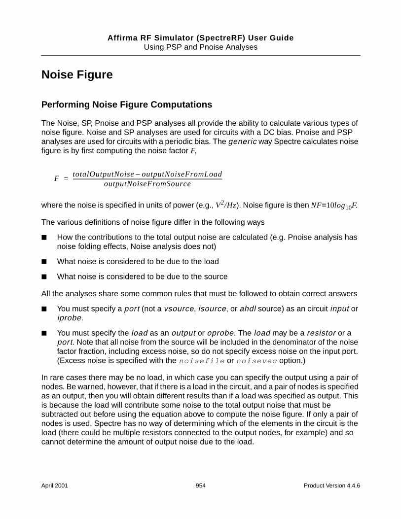
Affirma RF Simulator (SpectreRF) User GuideUsing PSP and Pnoise Analyses
Noise Figure
Performing Noise Figure Computations
The Noise, SP, Pnoise and PSP analyses all provide the ability to calculate various types ofnoise figure. Noise and SP analyses are used for circuits with a DC bias. Pnoise and PSPanalyses are used for circuits with a periodic bias. The generic way Spectre calculates noisefigure is by first computing the noise factor F,
where the noise is specified in units of power (e.g., V2/Hz). Noise figure is then NF=10log10F.
The various definitions of noise figure differ in the following ways
How the contributions to the total output noise are calculated (e.g. Pnoise analysis hasnoise folding effects, Noise analysis does not)
What noise is considered to be due to the load
What noise is considered to be due to the source
All the analyses share some common rules that must be followed to obtain correct answers
You must specify a port (not a vsource, isource, or ahdl source) as an circuit input oriprobe.
You must specify the load as an output or oprobe. The load may be a resistor or aport. Note that all noise from the source will be included in the denominator of the noisefactor fraction, including excess noise, so do not specify excess noise on the input port.(Excess noise is specified with the noisefile or noisevec option.)
In rare cases there may be no load, in which case you can specify the output using a pair ofnodes. Be warned, however, that if there is a load in the circuit, and a pair of nodes is specifiedas an output, then you will obtain different results than if a load was specified as output. Thisis because the load will contribute some noise to the total output noise that must besubtracted out before using the equation above to compute the noise figure. If only a pair ofnodes is used, Spectre has no way of determining which of the elements in the circuit is theload (there could be multiple resistors connected to the output nodes, for example) and socannot determine the amount of output noise due to the load.
FtotalOutputNoise outputNoiseFromLoad–
outputNoiseFromSource-----------------------------------------------------------------------------------------------------------------=
April 2001 954 Product Version 4.4.6
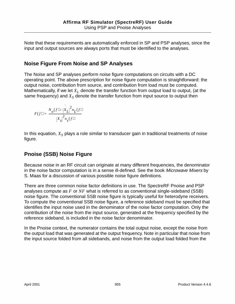
Affirma RF Simulator (SpectreRF) User GuideUsing PSP and Pnoise Analyses
Note that these requirements are automatically enforced in SP and PSP analyses, since theinput and output sources are always ports that must be identified to the analyses.
Noise Figure From Noise and SP Analyses
The Noise and SP analyses perform noise figure computations on circuits with a DCoperating point. The above prescription for noise figure computation is straightforward: theoutput noise, contribution from source, and contribution from load must be computed.Mathematically, if we let XL denote the transfer function from output load to output, (at thesame frequency) and XS denote the transfer function from input source to output then
In this equation, XS plays a role similar to transducer gain in traditional treatments of noisefigure.
Pnoise (SSB) Noise Figure
Because noise in an RF circuit can originate at many different frequencies, the denominatorin the noise factor computation is in a sense ill-defined. See the book Microwave Mixers byS. Maas for a discussion of various possible noise figure definitions.
There are three common noise factor definitions in use. The SpectreRF Pnoise and PSPanalyses compute as F or NF what is referred to as conventional single-sideband (SSB)noise figure. The conventional SSB noise figure is typically useful for heterodyne receivers.To compute the conventional SSB noise figure, a reference sideband must be specified thatidentifies the input noise used in the denominator of the noise factor computation. Only thecontribution of the noise from the input source, generated at the frequency specified by thereference sideband, is included in the noise factor denominator.
In the Pnoise context, the numerator contains the total output noise, except the noise fromthe output load that was generated at the output frequency. Note in particular that noise fromthe input source folded from all sidebands, and noise from the output load folded from the
F f( )No f( ) XL
2nL f( )–
Xs2
ns f( )---------------------------------------------------
˙
=
April 2001 955 Product Version 4.4.6

Affirma RF Simulator (SpectreRF) User GuideUsing PSP and Pnoise Analyses
non-zero sidebands, is included in the noise factor numerator. Mathematically, Pnoisecomputes conventional single-sideband noise factor as
where
fout is the output frequency swept by Pnoise
is the transfer function associated with the zero sideband, from load to output
is the transfer function associated with the reference sideband, from source tothe output
nL(fout) is noise generated by load at the output frequency
nS (fout+K ref f0) is the noise generated by the source at the input frequency.
In the PSP analysis context, the noise factor denominator includes only noise from the inputharmonic. The numerator contains all output noise, except noise from the output load at theoutput harmonic. (Refer to “Harmonics and Sidebands in PSP, PAC, PXF, and PnoiseAnalyses” on page 978 for a discussion of differences in frequency indexing in PXF and PSPanalyses.)
To be mathematically precise in what follows, let
denote the transfer function from output load, kth harmonic to output
denote the transfer function from input source, kth harmonic to output
Ko denote the output harmonic
Ki denote the input harmonic
The conventional single-sideband noise factor is computed by PSP as
Fssb f out( )No f out( ) XL
0( ) 2nL f out( )–
XS
Kref( ) 2nS f out Kref f 0+( )
------------------------------------------------------------------------------=
XL0( )
XsKref( )
XLK( )
XSK( )
Fssb f out( )No Ko f 0 f+( ) XL
Ko( ) 2nL Ko f 0 f+( )–
XS
Ki( ) 2nS Ki f 0 f+( )
------------------------------------------------------------------------------------------------------=
April 2001 956 Product Version 4.4.6
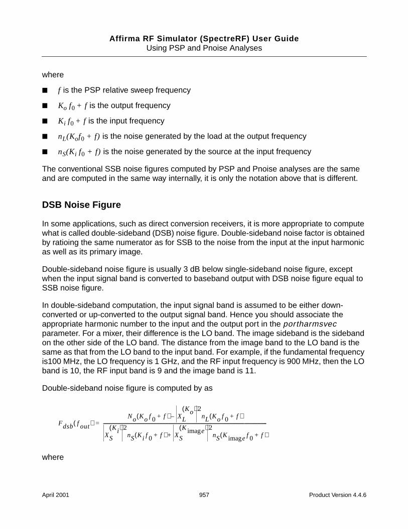
Affirma RF Simulator (SpectreRF) User GuideUsing PSP and Pnoise Analyses
where
f is the PSP relative sweep frequency
Ko f0 + f is the output frequency
Ki f0 + f is the input frequency
nL(Kof0 + f) is the noise generated by the load at the output frequency
nS(Ki f0 + f) is the noise generated by the source at the input frequency
The conventional SSB noise figures computed by PSP and Pnoise analyses are the sameand are computed in the same way internally, it is only the notation above that is different.
DSB Noise Figure
In some applications, such as direct conversion receivers, it is more appropriate to computewhat is called double-sideband (DSB) noise figure. Double-sideband noise factor is obtainedby ratioing the same numerator as for SSB to the noise from the input at the input harmonicas well as its primary image.
Double-sideband noise figure is usually 3 dB below single-sideband noise figure, exceptwhen the input signal band is converted to baseband output with DSB noise figure equal toSSB noise figure.
In double-sideband computation, the input signal band is assumed to be either down-converted or up-converted to the output signal band. Hence you should associate theappropriate harmonic number to the input and the output port in the portharmsvecparameter. For a mixer, their difference is the LO band. The image sideband is the sidebandon the other side of the LO band. The distance from the image band to the LO band is thesame as that from the LO band to the input band. For example, if the fundamental frequencyis100 MHz, the LO frequency is 1 GHz, and the RF input frequency is 900 MHz, then the LOband is 10, the RF input band is 9 and the image band is 11.
Double-sideband noise figure is computed by as
where
Fdsb f out( )No Ko f 0 f+( ) XL
Ko( ) 2nL Ko f 0 f+( )–
XS
Ki( ) 2nS Ki f 0 f+( ) XS
K eimag( ) 2nS K eimag f 0 f+( )+
---------------------------------------------------------------------------------------------------------------------------------------------------=
April 2001 957 Product Version 4.4.6

Affirma RF Simulator (SpectreRF) User GuideUsing PSP and Pnoise Analyses
nS (Kimagef0 + f ) the noise generated by source at the image input frequency obtainedaccording to the above description.
All other quantities are the same as those in Fssb. Note that only the PSP analysis computesdouble-sideband noise figure.
IEEE Noise Figure
Sometimes it is desirable to define noise figure quantities where we assume that the noisefrom input images that are potentially filtered is not present. The IEEE definition of noisefigure in mixers differs from the conventional definition in that it does not include thecontribution to the output noise from the image sideband in the numerator of the noise factor.Spectre eliminates all image harmonics/sidebands from the output noise in the noise factornumerator when computing Fieee. Using the above notation, Fieee is
Only PSP analysis computes Fieee.
Figure 12-7 on page 959, Figure 12-8 on page 960, and Figure 12-9 on page 961 summarizethe treatment of the input source and output load for the various noise figure definitions.
Fieee
No Ko f 0 f+( ) XL
Ko( ) 2nL Ko f 0 f+( )– XS
K( ) 2nS K f 0 f+( )
K Ki≠∑–
XS
Ki( ) 2nS Ki f 0 f+( )
----------------------------------------------------------------------------------------------------------------------------------------------------------------------------------=
April 2001 958 Product Version 4.4.6
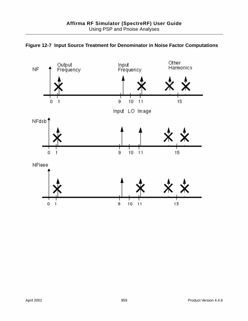
Affirma RF Simulator (SpectreRF) User GuideUsing PSP and Pnoise Analyses
Figure 12-7 Input Source Treatment for Denominator in Noise Factor Computations
April 2001 959 Product Version 4.4.6
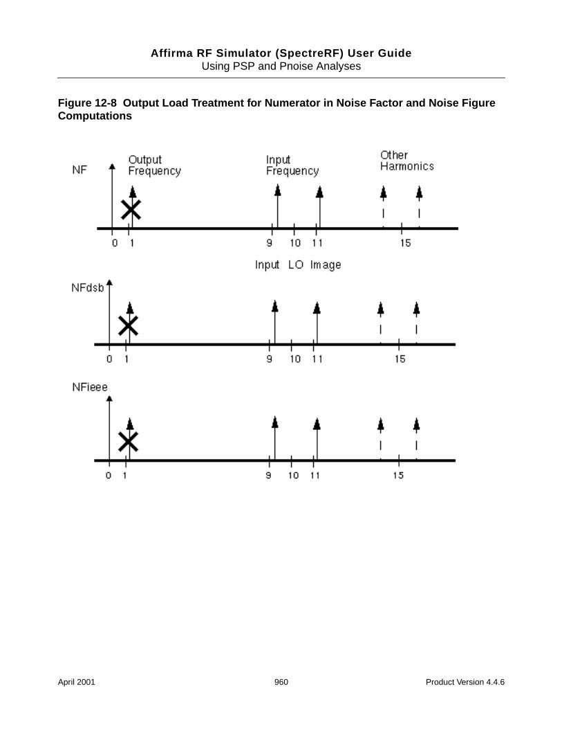
Affirma RF Simulator (SpectreRF) User GuideUsing PSP and Pnoise Analyses
Figure 12-8 Output Load Treatment for Numerator in Noise Factor and Noise FigureComputations
April 2001 960 Product Version 4.4.6
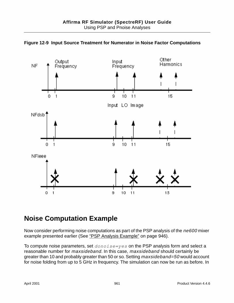
Affirma RF Simulator (SpectreRF) User GuideUsing PSP and Pnoise Analyses
Figure 12-9 Input Source Treatment for Numerator in Noise Factor Computations
Noise Computation Example
Now consider performing noise computations as part of the PSP analysis of the ne600 mixerexample presented earlier (See “PSP Analysis Example” on page 946).
To compute noise parameters, set donoise=yes on the PSP analysis form and select areasonable number for maxsideband. In this case, maxsideband should certainly begreater than 10 and probably greater than 50 or so. Setting maxsideband=50 would accountfor noise folding from up to 5 GHz in frequency. The simulation can now be run as before. In
April 2001 961 Product Version 4.4.6
Affirma RF Simulator (SpectreRF) User GuideUsing PSP and Pnoise Analyses
addition to computing the periodic S-parameters, the periodic noise correlation matrices willalso be computed, as will noise figure and the equivalent noise parameters.
Recall that the output axes for PSP analysis are set by the freqaxis option and are sharedby all quantities calculated by PSP analysis. This can seem odd in the case of noise figure,where the output noise is actually analyzed for the frequency range of 80 Mhz to 130 MHz.This is because the output harmonic is 1, representing a center frequency of 100 Mhz for therelative sweep, and the sweep ran from -20 MHz to 30 MHz. Setting freqaxis=out in thisexample would produce an axis running from 80 Mhz to 130 Mhz.
Input Referred Noise
For a given output noise spectrum, the equivalent input noise, input referred noise or IRN,is the noise that, if it were generated by the circuit element specified as input, would producethe same output noise. This assumes that the circuit loading conditions, etc., are unchanged.Note that the equivalent input noise will include noise from the source and load if they arenoisy in the original circuit. For example, consider a circuit with a voltage source as input, asin Figure 12-10 on page 963. If a voltage source inserted in series with the input sourcegenerates the input referred noise, and the rest of the circuit is noiseless, the noise observedat the output will be the same as in the original noisy circuit.
April 2001 962 Product Version 4.4.6
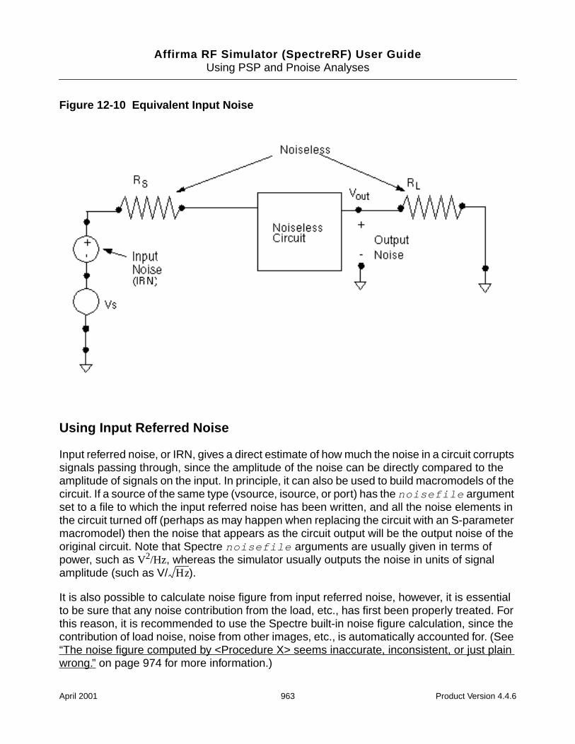
Affirma RF Simulator (SpectreRF) User GuideUsing PSP and Pnoise Analyses
Figure 12-10 Equivalent Input Noise
Using Input Referred Noise
Input referred noise, or IRN, gives a direct estimate of how much the noise in a circuit corruptssignals passing through, since the amplitude of the noise can be directly compared to theamplitude of signals on the input. In principle, it can also be used to build macromodels of thecircuit. If a source of the same type (vsource, isource, or port) has the noisefile argumentset to a file to which the input referred noise has been written, and all the noise elements inthe circuit turned off (perhaps as may happen when replacing the circuit with an S-parametermacromodel) then the noise that appears as the circuit output will be the output noise of theoriginal circuit. Note that Spectre noisefile arguments are usually given in terms ofpower, such as V2/Hz, whereas the simulator usually outputs the noise in units of signalamplitude (such as V/ ).
It is also possible to calculate noise figure from input referred noise, however, it is essentialto be sure that any noise contribution from the load, etc., has first been properly treated. Forthis reason, it is recommended to use the Spectre built-in noise figure calculation, since thecontribution of load noise, noise from other images, etc., is automatically accounted for. (See“The noise figure computed by <Procedure X> seems inaccurate, inconsistent, or just plainwrong.” on page 974 for more information.)
Hz
April 2001 963 Product Version 4.4.6
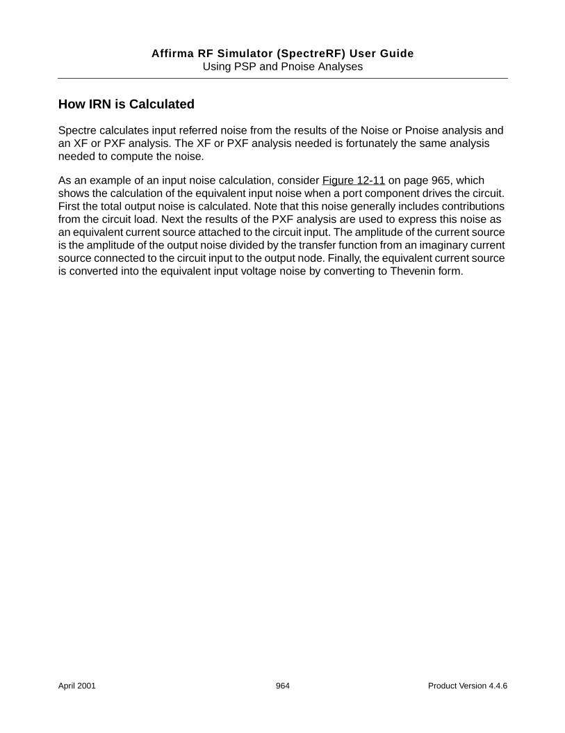
Affirma RF Simulator (SpectreRF) User GuideUsing PSP and Pnoise Analyses
How IRN is Calculated
Spectre calculates input referred noise from the results of the Noise or Pnoise analysis andan XF or PXF analysis. The XF or PXF analysis needed is fortunately the same analysisneeded to compute the noise.
As an example of an input noise calculation, consider Figure 12-11 on page 965, whichshows the calculation of the equivalent input noise when a port component drives the circuit.First the total output noise is calculated. Note that this noise generally includes contributionsfrom the circuit load. Next the results of the PXF analysis are used to express this noise asan equivalent current source attached to the circuit input. The amplitude of the current sourceis the amplitude of the output noise divided by the transfer function from an imaginary currentsource connected to the circuit input to the output node. Finally, the equivalent current sourceis converted into the equivalent input voltage noise by converting to Thevenin form.
April 2001 964 Product Version 4.4.6
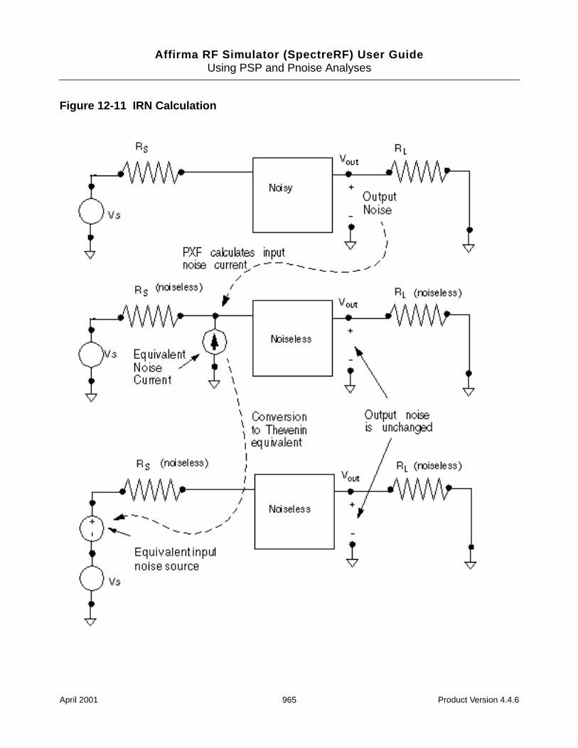
Affirma RF Simulator (SpectreRF) User GuideUsing PSP and Pnoise Analyses
Figure 12-11 IRN Calculation
April 2001 965 Product Version 4.4.6
Affirma RF Simulator (SpectreRF) User GuideUsing PSP and Pnoise Analyses
Relation to Gain
It is common to think of the input noise as the output noise divided by the gain,
where the output noise and input noise are measured in volts/ . This is a true statement ifthe proper gain is used. The gain reported by Pnoise analysis is in fact the ratio between theoutput noise and the equivalent input noise as computed in the previous section. However,the gain reported by Pnoise analysis is not necessarily the gain useful for any other purposes(see “Gain Calculations in Pnoise” on page 971).
Referring Noise to Ports
A port component in Spectre is a voltage source combined with a resistive impedance. Portsexist to enable easy generation of test fixtures, accurate noise figure calculations, and S-parameter calculations. Noise and S-parameter calculations in Spectre can (usually) only beproperly performed when ports are used to drive the input and output. While the port iselectrically equivalent to a source + resistor, the excitations are specified in a somewhatdifferent way.
The port component is designed so that when a 1 V source is specified, 1 V appears at theport output when the circuit impedance is matched to the port reference impedance. The portoutput, however, is not the internal node that connects the voltage source and resistor, butrather the exterior resistor terminal that actually connects to the circuit under test. Thus, asshown in Figure 12-12 on page 967, the voltage on the internal voltage source must be twicethe voltage specified to appear at the port output.
One implication of this convention is that when a port is specified as an input in Pnoiseanalysis it is the noise referred to the port that is computed, not the noise referred to theinternal voltage source. In other words, the input equivalent noise reported is the noise thatwould be fed back to spectre as a noisefile argument on the port to produce the same outputnoise. The noise referred to the port will have amplitude half of the noise referred to the inputvoltage source.
Likewise, the gain reported by Spectre is the gain that would produce the equivalent inputnoise, referred to the port. It will be half the gain from the input voltage source.
IRNOutputNoise
G---------------------------------=
Hz
April 2001 966 Product Version 4.4.6
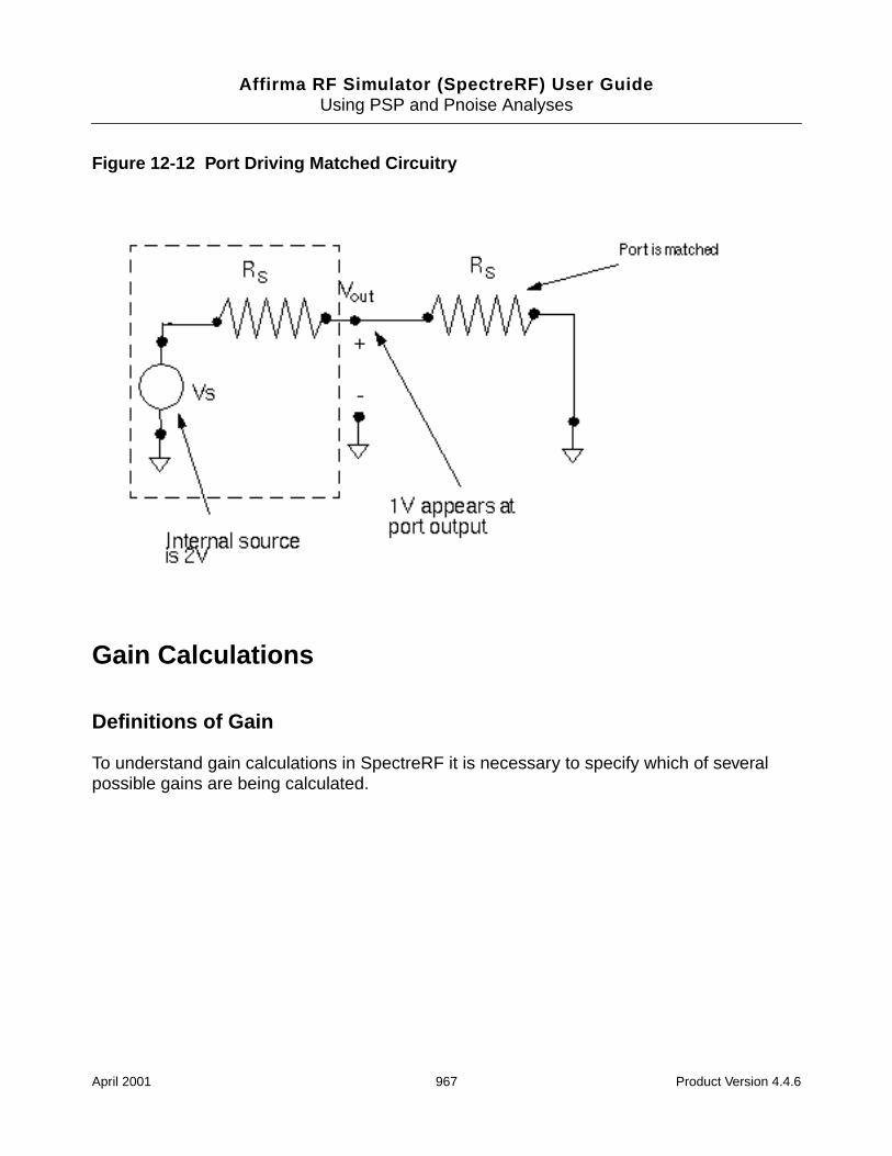
Affirma RF Simulator (SpectreRF) User GuideUsing PSP and Pnoise Analyses
Figure 12-12 Port Driving Matched Circuitry
Gain Calculations
Definitions of Gain
To understand gain calculations in SpectreRF it is necessary to specify which of severalpossible gains are being calculated.
April 2001 967 Product Version 4.4.6
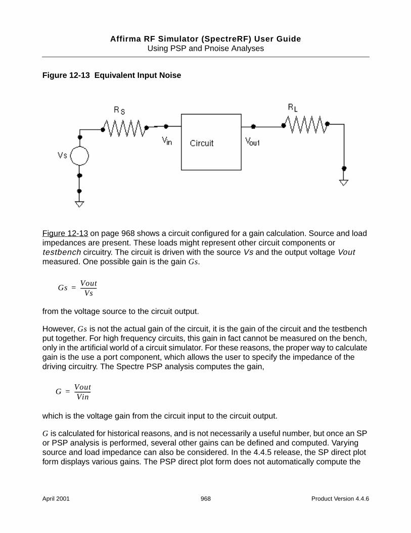
Affirma RF Simulator (SpectreRF) User GuideUsing PSP and Pnoise Analyses
Figure 12-13 Equivalent Input Noise
Figure 12-13 on page 968 shows a circuit configured for a gain calculation. Source and loadimpedances are present. These loads might represent other circuit components ortestbench circuitry. The circuit is driven with the source Vs and the output voltage Voutmeasured. One possible gain is the gain Gs.
from the voltage source to the circuit output.
However, Gs is not the actual gain of the circuit, it is the gain of the circuit and the testbenchput together. For high frequency circuits, this gain in fact cannot be measured on the bench,only in the artificial world of a circuit simulator. For these reasons, the proper way to calculategain is the use a port component, which allows the user to specify the impedance of thedriving circuitry. The Spectre PSP analysis computes the gain,
which is the voltage gain from the circuit input to the circuit output.
G is calculated for historical reasons, and is not necessarily a useful number, but once an SPor PSP analysis is performed, several other gains can be defined and computed. Varyingsource and load impedance can also be considered. In the 4.4.5 release, the SP direct plotform displays various gains. The PSP direct plot form does not automatically compute the
GsVoutVs
------------=
GVoutVin
------------=
April 2001 968 Product Version 4.4.6
Affirma RF Simulator (SpectreRF) User GuideUsing PSP and Pnoise Analyses
various gains but they can be computed from the basic definitions using the waveformcalculator.
Some gains of interest in two-port circuits are:
GA (Available Gain)
GP (Power Gain)
GT (Transducer Gain)
Gumx (Maximum Unilateral Transducer Power Gain)
Gmax (Maximum Available Gain)
GA (Available Gain) , the power gain obtained by optimally (conjugately) matching theoutput of the network.
where
and ΓS is the source reflection coefficient,
with ZS is the source impedance and ZS, refis the reference impedance for the input port.
GA
S212
1 ΓS2
–( )
1 S11ΓS–2
1 Γ22
–( )---------------------------------------------------------=
Γ2 S22
S12S21ΓS1 S11ΓS–------------------------+=
ΓS
ZS ZS ref,–
ZS ZS ref,+-------------------------------=
April 2001 969 Product Version 4.4.6
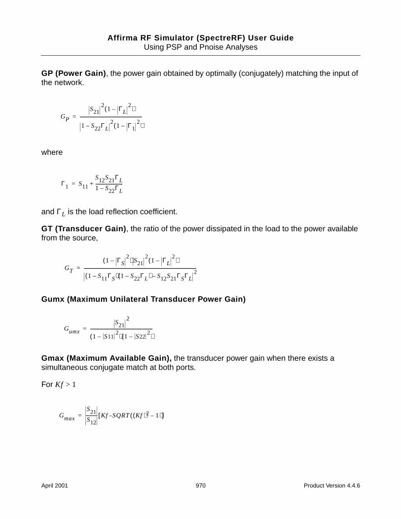
Affirma RF Simulator (SpectreRF) User GuideUsing PSP and Pnoise Analyses
GP (Power Gain) , the power gain obtained by optimally (conjugately) matching the input ofthe network.
where
and ΓL is the load reflection coefficient.
GT (Transducer Gain) , the ratio of the power dissipated in the load to the power availablefrom the source,
Gumx (Maximum Unilateral Transducer Power Gain)
Gmax (Maximum Available Gain), the transducer power gain when there exists asimultaneous conjugate match at both ports.
For Kf > 1
GP
S212
1 ΓL2
–( )
1 S22ΓL–2
1 Γ12
–( )---------------------------------------------------------=
Γ1 S11
S12S21ΓL1 S22ΓL–-------------------------+=
GT
1 ΓS2
–( ) S212
1 ΓL2
–( )
1 S11ΓS–( ) 1 S22ΓL–( ) S12S21ΓSΓL–2
-------------------------------------------------------------------------------------------------------=
Gumx
S212
1 S112
–( ) 1 S222
–( )---------------------------------------------------------=
Gmax
S21S12----------- Kf S– QRT Kf( )2 1–( )[ ]=
April 2001 970 Product Version 4.4.6
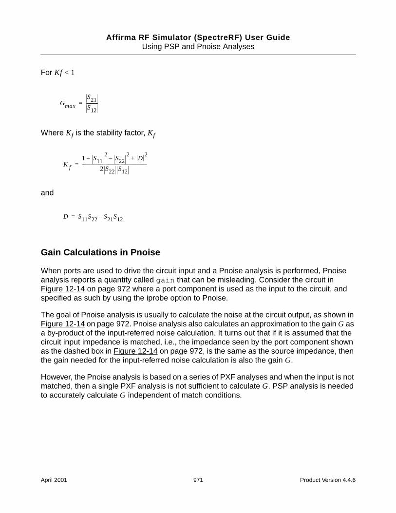
Affirma RF Simulator (SpectreRF) User GuideUsing PSP and Pnoise Analyses
For Kf < 1
Where Kf is the stability factor, Kf
and
Gain Calculations in Pnoise
When ports are used to drive the circuit input and a Pnoise analysis is performed, Pnoiseanalysis reports a quantity called gain that can be misleading. Consider the circuit inFigure 12-14 on page 972 where a port component is used as the input to the circuit, andspecified as such by using the iprobe option to Pnoise.
The goal of Pnoise analysis is usually to calculate the noise at the circuit output, as shown inFigure 12-14 on page 972. Pnoise analysis also calculates an approximation to the gain G asa by-product of the input-referred noise calculation. It turns out that if it is assumed that thecircuit input impedance is matched, i.e., the impedance seen by the port component shownas the dashed box in Figure 12-14 on page 972, is the same as the source impedance, thenthe gain needed for the input-referred noise calculation is also the gain G.
However, the Pnoise analysis is based on a series of PXF analyses and when the input is notmatched, then a single PXF analysis is not sufficient to calculate G. PSP analysis is neededto accurately calculate G independent of match conditions.
Gmax
S21S12-----------=
K f
1 S112
– S222
– D2
+
2 S22 S12------------------------------------------------------------=
D S11S22 S21S12–=
April 2001 971 Product Version 4.4.6
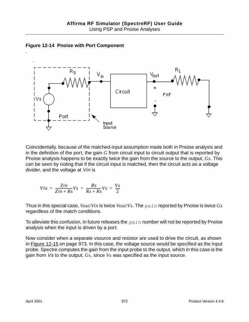
Affirma RF Simulator (SpectreRF) User GuideUsing PSP and Pnoise Analyses
Figure 12-14 Pnoise with Port Component.
Coincidentally, because of the matched-input assumption made both in Pnoise analysis andin the definition of the port, the gain G from circuit input to circuit output that is reported byPnoise analysis happens to be exactly twice the gain from the source to the output, Gs. Thiscan be seen by noting that if the circuit input is matched, then the circuit acts as a voltagedivider, and the voltage at Vin is
Thus in this special case, Vout/Vin is twice Vout/Vs. The gain reported by Pnoise is twice Gsregardless of the match conditions.
To alleviate this confusion, in future releases the gain number will not be reported by Pnoiseanalysis when the input is driven by a port.
Now consider when a separate vsource and resistor are used to drive the circuit, as shownin Figure 12-15 on page 973. In this case, the voltage source would be specified as the inputprobe. Spectre computes the gain from the input probe to the output, which in this case is thegain from Vs to the output, Gs, since Vs was specified as the input source.
VinZin
Zin Rs+---------------------Vs
RsRs Rs+-------------------Vs
Vs2
------= = =
April 2001 972 Product Version 4.4.6
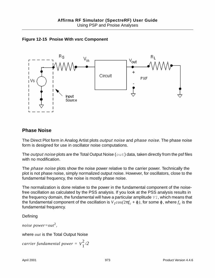
Affirma RF Simulator (SpectreRF) User GuideUsing PSP and Pnoise Analyses
Figure 12-15 Pnoise With vsrc Component
Phase Noise
The Direct Plot form in Analog Artist plots output noise and phase noise. The phase noiseform is designed for use in oscillator noise computations.
The output noise plots are the Total Output Noise (out ) data, taken directly from the psf fileswith no modification.
The phase noise plots show the noise power relative to the carrier power. Technically theplot is not phase noise, simply normalized output noise. However, for oscillators, close to thefundamental frequency, the noise is mostly phase noise.
The normalization is done relative to the power in the fundamental component of the noise-free oscillation as calculated by the PSS analysis. If you look at the PSS analysis results inthe frequency domain, the fundamental will have a particular amplitude V1, which means thatthe fundamental component of the oscillation is V1cos(2πfc + ϕ), for some ϕ, where fc is thefundamental frequency.
Defining
noise power=out2,
where out is the Total Output Noise
carrier fundamental power = /2V12
April 2001 973 Product Version 4.4.6

Affirma RF Simulator (SpectreRF) User GuideUsing PSP and Pnoise Analyses
the normalized power is
normalized power = (out2)/[ /2]
Thus the formula used by Direct Plot in Artist 4.4.3 and later to plot the normalized power(phase noise) in dB10 is:
normalized power in dB =10log10( out2)/[ /2]
For more information on phase noise, see Appendix A, “Oscillator Noise Analysis,” whichsummarizes how to get good phase noise calculations.
Frequently Asked Questions
The noise figure computed by <Procedure X> seems inaccurate, inconsistent, orjust plain wrong.
The key to noise figure computation is to remember that three pieces of information areneeded:
The total noise at the output
How much of that noise is due to the output load
How much of that noise is due to the input source
Noise figure is the log of noise factor, and noise factor is fundamentally the total output noiseless the noise due to the load ratioed to the noise due to the input. The easiest way to be sureof getting the correct noise figure is to use ports as input and output sources and loads andto have the Spectre simulator perform the noise figure computation.
SpectreRF correctly accounts for the noise due to the load, as well as the different possibletreatments of noise from the input source that result in different types of noise figure that areused in RF circuits (customary SSB, IEEE SSB, DSB, as discussed in “Noise Figure” onpage 954). See “Performing Noise Figure Computations” on page 954 for information onsetting up noise figure computation.
Most mistakes in noise figure calculations arise when improperly accounting for items twoand three in the list above. Hand computations of noise figure require that you correctlyaccount for noise from the load and source, which can be difficult. For example, some usershave tried to use the information from the noise summary table to calculate noise figure. Thenoise summary table reports total noise contributions, from all sidebands present in thePnoise analysis, sorted by contributor. If the total noise reported in the noise summary is used
V12
V12
April 2001 974 Product Version 4.4.6
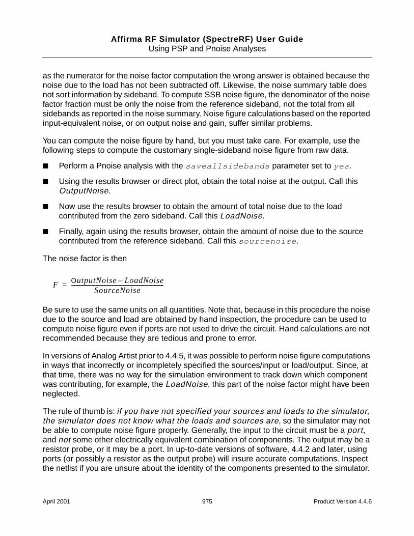
Affirma RF Simulator (SpectreRF) User GuideUsing PSP and Pnoise Analyses
as the numerator for the noise factor computation the wrong answer is obtained because thenoise due to the load has not been subtracted off. Likewise, the noise summary table doesnot sort information by sideband. To compute SSB noise figure, the denominator of the noisefactor fraction must be only the noise from the reference sideband, not the total from allsidebands as reported in the noise summary. Noise figure calculations based on the reportedinput-equivalent noise, or on output noise and gain, suffer similar problems.
You can compute the noise figure by hand, but you must take care. For example, use thefollowing steps to compute the customary single-sideband noise figure from raw data.
Perform a Pnoise analysis with the saveallsidebands parameter set to yes .
Using the results browser or direct plot, obtain the total noise at the output. Call thisOutputNoise.
Now use the results browser to obtain the amount of total noise due to the loadcontributed from the zero sideband. Call this LoadNoise.
Finally, again using the results browser, obtain the amount of noise due to the sourcecontributed from the reference sideband. Call this sourcenoise .
The noise factor is then
Be sure to use the same units on all quantities. Note that, because in this procedure the noisedue to the source and load are obtained by hand inspection, the procedure can be used tocompute noise figure even if ports are not used to drive the circuit. Hand calculations are notrecommended because they are tedious and prone to error.
In versions of Analog Artist prior to 4.4.5, it was possible to perform noise figure computationsin ways that incorrectly or incompletely specified the sources/input or load/output. Since, atthat time, there was no way for the simulation environment to track down which componentwas contributing, for example, the LoadNoise, this part of the noise factor might have beenneglected.
The rule of thumb is: if you have not specified your sources and loads to the simulator,the simulator does not know what the loads and sources are, so the simulator may notbe able to compute noise figure properly. Generally, the input to the circuit must be a port,and not some other electrically equivalent combination of components. The output may be aresistor probe, or it may be a port. In up-to-date versions of software, 4.4.2 and later, usingports (or possibly a resistor as the output probe) will insure accurate computations. Inspectthe netlist if you are unsure about the identity of the components presented to the simulator.
FOutputNoise LoadNoise–
SourceNoise--------------------------------------------------------------------=
April 2001 975 Product Version 4.4.6
Affirma RF Simulator (SpectreRF) User GuideUsing PSP and Pnoise Analyses
Finally, if you ever have any doubt about the propriety of the procedure you are using, use theresults browser to access the noise figure directly from the simulation data. This data iscorrect in all software versions.
Why is the gain reported by Pnoise twice the gain that I expect?
First, unlike some circuit simulators, Pnoise and PSP compute the gain of the circuit fromits input to its output, instead of from an external source to the output. See “Definitionsof Gain” on page 967 to see if the gain you expect is actually the gain that you want.
Second, Pnoise makes certain assumptions about input matching in order to calculatethis gain. See “Gain Calculations in Pnoise” on page 971 for further explanations of theway Pnoise calculates gain.
In general, you should not use the gain calculated by Pnoise unless you know your circuit isinput-matched. Use PSP instead.
Does SpectreRF compute single-sideband (SSB) or double-sideband (DSB) noisefigure?
The SpectreRF Pnoise analysis computes SSB noise figure, (except in certain specialcases). PSP can compute both SSB and DSB noise figure. See “Noise Figure” on page 954.
Why does the axis for noise or noise figure have negative frequencies?
The axis labeling in Spectre is fairly independent of the actual computation. In all cases,Spectre computes single-sided noise (that is, there is no need to add noise from negativefrequencies to get the total noise power or noise figure).
Recall that PSP analysis performs many computations at once—periodic S-parameters,noise correlation matrices, noise figure, etc. In 4.4.5, for historical reasons, all thesequantities are stored as a sweep with a single axis. An axis appropriate for visualizing s11may not be good to display NF.
To obtain strictly positive axis labels for noise quantities in PSP, choose a positive integer forthe output harmonic, use sweeptype=relative, and set freqaxis=out on the PSP analysisoptions form.
April 2001 976 Product Version 4.4.6
Affirma RF Simulator (SpectreRF) User GuideUsing PSP and Pnoise Analyses
How does match affect the noise and gain calculations in SpectreRF?
If the input impedance is not matched to the port impedance, the gain and input referrednoise, or IRN, reported by Pnoise analysis is probably not the gain you want. out , F, NF,and in (input-referred noise) will still be correct.
PSP analysis computes the correct G, in (input-referred noise), F and NF regardless ofmatch.
Will Spectre include noise parameter data from S-parameter files?
Spectre supports writing and reading S-parameter files, but as of the 4.4.5 release it does notwrite noise parameter data into files, nor can noise parameter data be read from file andincluded in a simulation.
Known Problems and Limitations
Dubious AC-Noise Analysis Features
When computing noise figure in circuits with a DC bias point in releases prior to 4.4.5, thenoise figure available from the direct plot form was obtained from knowledge of the totaloutput noise computed with a Noise analysis, the source impedance as entered on a form,and circuit gain data obtained in an auxiliary AC analysis. Simulators other than Spectre stillrequire this procedure.
In 4.4.5, if you use ports as the output load and input source, the noise figure is obtaineddirectly from the Spectre simulator data. An artifact of the previous use model is that the noisefigure direct plot still requires an AC analysis to run, but this analysis has no effect on thecomputed noise figure if ports are used as sources and loads.
If ports are not used as the input source and load (for example, using a vsin component asthe input and a pair of nodes as the output) it is still possible to compute noise figure in theAnalog Artist environment, but the procedure is not recommended as it can be tricky to obtainthe desired result (see “Performing Noise Figure Computations” on page 954 and “The noisefigure computed by <Procedure X> seems inaccurate, inconsistent, or just plain wrong.” onpage 974).
To obtain reasonable noise figure calculations using this (unsupported) procedure, you mustconfigure the circuit as shown in Figure 12-16 on page 978. Be sure to select the propernodes as input and output (note that a port component cannot be used in this topologybecause the Vin node cannot be accessed). The contribution of the output load to the total
April 2001 977 Product Version 4.4.6
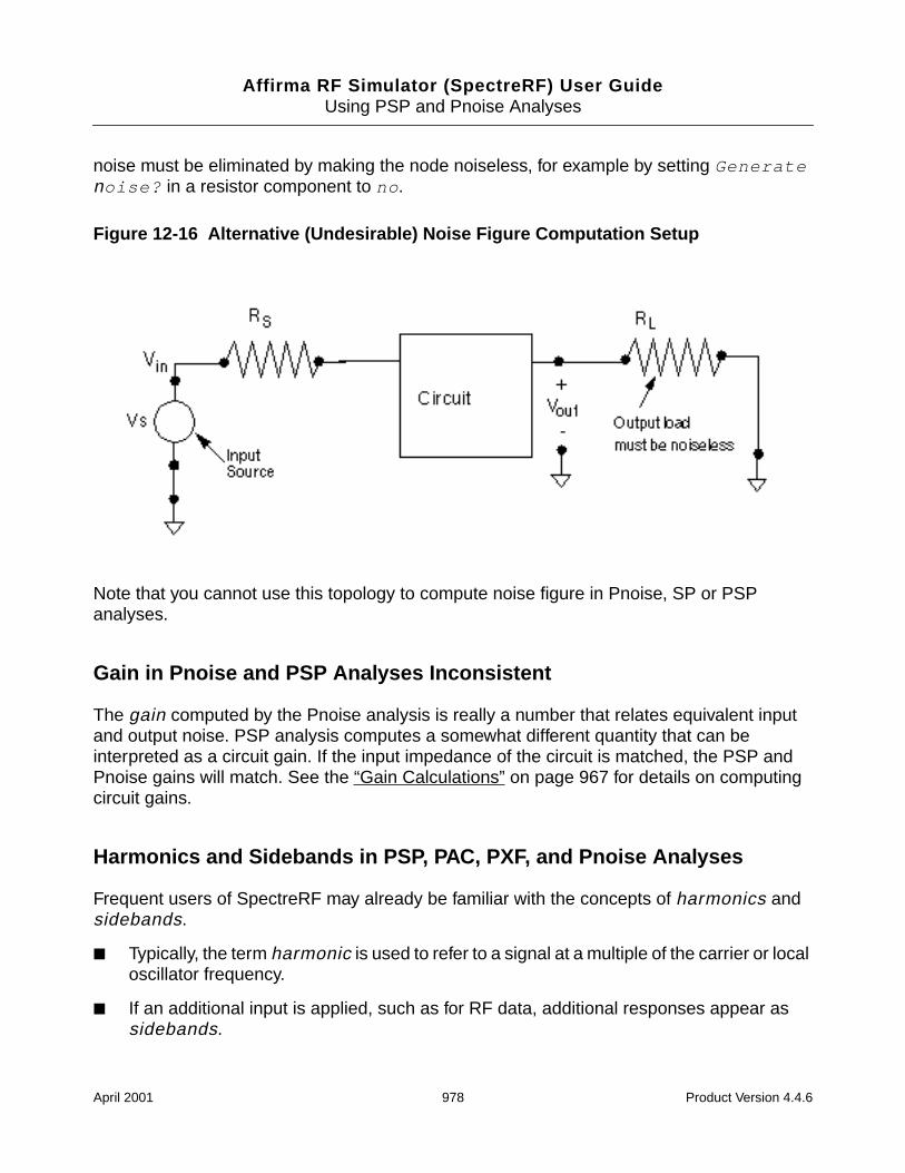
Affirma RF Simulator (SpectreRF) User GuideUsing PSP and Pnoise Analyses
noise must be eliminated by making the node noiseless, for example by setting Generatenoise? in a resistor component to no .
Figure 12-16 Alternative (Undesirable) Noise Figure Computation Setup
Note that you cannot use this topology to compute noise figure in Pnoise, SP or PSPanalyses.
Gain in Pnoise and PSP Analyses Inconsistent
The gain computed by the Pnoise analysis is really a number that relates equivalent inputand output noise. PSP analysis computes a somewhat different quantity that can beinterpreted as a circuit gain. If the input impedance of the circuit is matched, the PSP andPnoise gains will match. See the “Gain Calculations” on page 967 for details on computingcircuit gains.
Harmonics and Sidebands in PSP, PAC, PXF, and Pnoise Analyses
Frequent users of SpectreRF may already be familiar with the concepts of harmonics andsidebands.
Typically, the term harmonic is used to refer to a signal at a multiple of the carrier or localoscillator frequency.
If an additional input is applied, such as for RF data, additional responses appear assidebands.
April 2001 978 Product Version 4.4.6
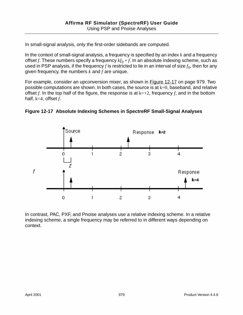
Affirma RF Simulator (SpectreRF) User GuideUsing PSP and Pnoise Analyses
In small-signal analysis, only the first-order sidebands are computed.
In the context of small-signal analysis, a frequency is specified by an index k and a frequencyoffset f. These numbers specify a frequency kf0 + f. In an absolute indexing scheme, such asused in PSP analysis, if the frequency f is restricted to lie in an interval of size f0, then for anygiven frequency, the numbers k and f are unique.
For example, consider an upconversion mixer, as shown in Figure 12-17 on page 979. Twopossible computations are shown. In both cases, the source is at k=0, baseband, and relativeoffset f. In the top half of the figure, the response is at k=+2, frequency f, and in the bottomhalf, k=4, offset f.
Figure 12-17 Absolute Indexing Schemes in SpectreRF Small-Signal Analyses
In contrast, PAC, PXF, and Pnoise analyses use a relative indexing scheme. In a relativeindexing scheme, a single frequency may be referred to in different ways depending oncontext.
April 2001 979 Product Version 4.4.6
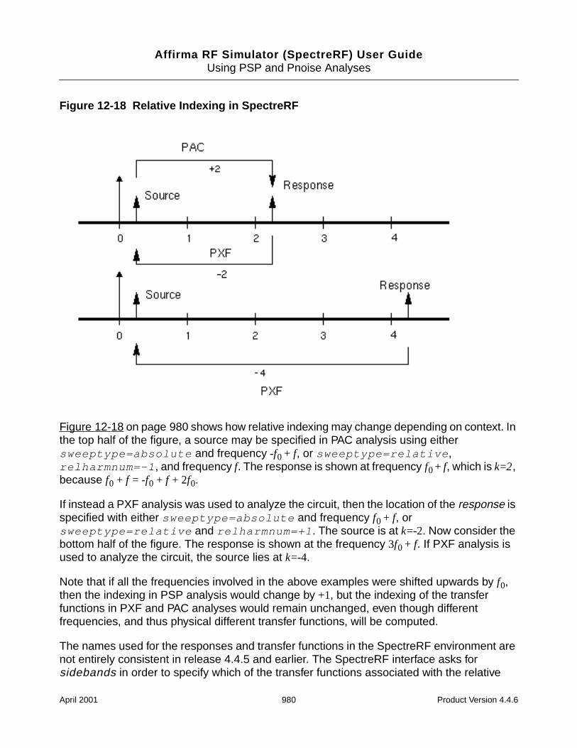
Affirma RF Simulator (SpectreRF) User GuideUsing PSP and Pnoise Analyses
Figure 12-18 Relative Indexing in SpectreRF
Figure 12-18 on page 980 shows how relative indexing may change depending on context. Inthe top half of the figure, a source may be specified in PAC analysis using eithersweeptype=absolute and frequency -f0 + f, or sweeptype=relative ,relharmnum=-1 , and frequency f. The response is shown at frequency f0+ f, which is k=2,because f0 + f = -f0 + f + 2f0.
If instead a PXF analysis was used to analyze the circuit, then the location of the response isspecified with either sweeptype=absolute and frequency f0 + f, orsweeptype=relative and relharmnum=+1 . The source is at k=-2. Now consider thebottom half of the figure. The response is shown at the frequency 3f0 + f. If PXF analysis isused to analyze the circuit, the source lies at k=-4.
Note that if all the frequencies involved in the above examples were shifted upwards by f0,then the indexing in PSP analysis would change by +1, but the indexing of the transferfunctions in PXF and PAC analyses would remain unchanged, even though differentfrequencies, and thus physical different transfer functions, will be computed.
The names used for the responses and transfer functions in the SpectreRF environment arenot entirely consistent in release 4.4.5 and earlier. The SpectreRF interface asks forsidebands in order to specify which of the transfer functions associated with the relative
April 2001 980 Product Version 4.4.6

Affirma RF Simulator (SpectreRF) User GuideUsing PSP and Pnoise Analyses
index k are wanted. This is reasonable because the small-signal responses appear assidebands to the harmonics of the fundamental frequency of the PSS steady-state solution.However, the data is output and displayed with the label harmonic. Thus the index namingis not consistent. However, since the transfer function associated with the relative index kresults from the small-signal being convolved with the kth harmonic of the steady-statesolution, the harmonic label is not entirely inappropriate either.
April 2001 981 Product Version 4.4.6
Affirma RF Simulator (SpectreRF) User Guide
Index
Symbols./.inilmg file, in LMG 333
Numerics1dB compression point
low noise amplifier, plotting 301on Results forms 132
1st Order Harmonic 1303rd Order Harmonic 130
AAccuracy Defaults specification 99, 124
conservative 124liberal 124moderate 124
accuracy parametersallglobal 123, 124alllocal 123, 124lteratio 123, 124maxacfreq 123maxperiods 124pointlocal 123relref 123, 124sigglobal 123, 124steadyratio 123, 124
accuracy, of LMG models 340Add Specific Points, entry on Choosing
Analyses form 100Add to Outputs specification, on Results
forms 130Additional Time for Stabilization, entry on
Choosing Analyses form 100allglobal parameter 123, 124alllocal parameter 123, 124Analog Artist Design Environment, using
PKG in 381analysis
descriptions 26, 32, 40, 43Analysis type specification, on Results
forms 130annotate parameter 124
annotation parametersannotate 124stats 124
assumptionsfor large and moderate signal analyses
Pdisto 23for large-signal analyses
linearity assumption with PSS 22periodicity assumption with PSS/
SPSS 22for small signal analyses 25
linearity 25Auto Calculate Button 100autodc parameter 125Automatic Sweep Type setting 120
Bbond wire
shape functionshape functions, in PKG 370
Bond Wire Diameter type-in field, inPKG 370
bond wire file format, in PKG 371Bond Wire Length type-in field, in PKG 370Bond Wire Number type-in field, in
PKG 369bond wire setup button 354Bond Wire Setup form, in PKG 367
function buttons 367menu buttons 367
bond wire setup, in PKG 348bond wire shape functions
shape function, in PKG 367Bonding Pad Height type-in field, in
PKG 357Bondpad Coord (Yb) type-in field, in
PKG 365Bondpad Length (Lb) type-in field, in
PKG 365Bondpad Width (Wb) type-in field, in
PKG 365building blocks, in PKG 347
April 2001 982 Product Version 4.4.6
Affirma RF Simulator (SpectreRF) User Guide
CCadence libraries, setting up 140, 141Calculate Capacitance buttons, in
PKG 373Calculate Inductance buttons, in PKG 375Calculate Parameters function button, in
LMG 326, 330Cancel button, in PKG 377Capacitance Accuracy buttons, in
PKG 374capacitance calculation, in PKG 349Center - Span specification, Frequency
Sweep Range (Hz) fields 102Choosing Analyses form 99
Accuracy Defaults specification 99Analysis specification 100Auto Calculate Button 100Do Noise 101Enabled button 101Frequency (Hz) field 101, 107Frequency Sweep Range (Hz)
fields 101Center - Span specification 102Single - Point specification 102Start - Stop specification 102
Input Source specification 104, 105Input Voltage Source specification 105Options specification 106Oscillator button 106Output
harmonics selection 108Number of harmonics 109
Output harmonics selectionArray of harmonics 110, 115Select from range 109
Output specification for Pnoise andPXF 101, 106
PAC analysiswith PSS 60with SPSS 61
Pdisto analysis 59Periodic Steady-State analysis 56, 57Periodic Steady-State analysis with
sweep 58Pnoise analysis
with PSS 62with SPSS 63
PSS analysis 55PXF analysis
with PSS 64with SPSS 65
Reference Sideband specification 111,112
Relative to Fundamental button 112Save Initial Transient Results
specification 112Select button 113Select Ports 112Sidebands specification 113
Maximum sideband 101, 114Select from range 114
Small Signal Periodic Analysis listbox 116
Sweep Range (Hz) specificationCenter - Span 118Start - Stop 118
Sweep specification 116variable 116
Sweep TypeAutomatic 120Linear 121Logarithmic 121
Sweep Type specification 121Add Specific Points 122Linear 121Logarithmic 121
Clear/Add button, Fundamental Tones listbox 104
Close button, in PKG 377, 378cmin parameter 124compression parameter 127Conductivity type-in field
in LMG 326in PKG 370
Conductor Distances type-in field, inLMG 326
Conductor Height (h) type-in field, inLMG 326
Conductor Height type-in field, in LMG 330Conductor Length type-in field, in
LMG 326, 330Conductor Thickness type-in field, in
LMG 326, 330Conductor Width type-in field, in LMG 325,
330convergence parameters
cmin 124gear_order 125readns 124solver 125
April 2001 983 Product Version 4.4.6
Affirma RF Simulator (SpectreRF) User Guide
exp 125std 125turbo 125
tolerance 124conversion gain measurement, mixer 180
conversion gain, plotting 185power supply rejection, plotting 188
Coupled Pins Per Side type-in field, inPKG 377
Create button, in PKG 378Create DA Terminal type-in field, in
PKG 378Create Macromodel function button, in
LMG 326current
gain specification, on Resultsforms 132
specification, on Results forms 132
Ddata entry
Fundamental Tones list boxbuttons 102fields 102
data entry section on form in LMG 325dB20, as Results form modifier 135default values, in LMG 326Delete button 104Die Attach Height type-in field, in PKG 362Die Attach Length (Lda) type-in field, in
PKG 362die attach setup
button 354in PKG 361
Die Attach Thickness (Tda) type-in field, inPKG 362
Die Attach Width (Wda) type-in field, inPKG 362
Die Bond Site (x, y) type-in field, inPKG 370
Die Cavity Side buttons, in PKG 364Dielectric Constant type-in field
in LMG 329in PKG 374
Dielectric Thickness (d) type-in field, inLMG 325
Dielectric Thickness type-in field, inLMG 329
DIP packages, setup 359
display section on form, in LMG 325Do Noise, Choosing Analyses form 101
EEdit Object Properties form 383
use external model file button 336elevation (e) type-in field, in PKG 357Enabled button 101equivalent noise resistance, low noise
amplifier, plotting 285errpreset parameter 99euler parameter 126examples
low noise amplifier 2561dB compression point, plotting 301noise calculations 292output voltage distribution 261, 266PXF analysis 312S-parameter analysis 272
voltage standing wave ratio,plotting 278
S-parameter Noise analysis 279equivalent noise resistance,
plotting 285load stability circles, plotting 286minimum noise figure 282noise circles, plotting 290noise figure 282source stability circles 288
third-order intercept point,plotting 307
voltage gaincalculation 261plotting 264
mixerconversion gain measurement 180
conversion gain, plotting 185power supply rejection,
plotting 188harmonic distortion
measurement 151intermodulation distortion
measurementwith Pdisto 202
noise figure measurement 1601dB compression point 188
noise figure measurement withPSP 165
periodic S-parameter plots 165
April 2001 984 Product Version 4.4.6
Affirma RF Simulator (SpectreRF) User Guide
third-order intercept measurementwith PSS sweep andPAC 194
modeling transmission lines using theLMG form (use model one)
contents of example model 327setup 327
modeling transmission lines using theTransmission LIne Modeler form(use model one)
creating the model 327modeling transmission lines using the
Transmission Line Modeler form(use model one)
use of lumped models within AnalogArtist 334
modeling transmission lines withoutusing the Transmission LineModeler form (use modeltwo) 338
oscillator simulation, of differentialoscillator 241
output noise, plotting 252oscillator simulation, of tline3oscRF
phase noise, plotting 240steady state solution, plotting 238
package Modeling with a mixer usingPKG 385
executables, in PKG setup 350exp parameter value 125Expr field, Fundamental Tones list box 102Extrapolation Point specification, on Results
forms 130
FFASTCAP, in PKG 346FASTHENRY, in PKG 346File menu
Bond Wire Setup form 367in LMG 323
first-order harmonic specification, on Resultsforms 131
flicker noise computation 47Fmax type-in field, in LMG 326, 330forms
Choosing Analyses 99Options 70Results 130
Fourier analysis 26
freq. unit menu choice 354Freq. Unit menu choices, in LMG 325freqaxis parameter
absin 127in 127out 127
Frequency (Beat) specification,Fundamental Tones 100, 101
Frequency (Hz) field 101, 107Frequency Sweep Range (Hz) fields 101function
buttons, in LMG 322buttons, in PKG main window 354buttons, in PKG RF IC Package Modeler
windowbond wire setup 354die attach setup 354package dimension setup 354
specification, on Results forms 131function buttons
in LMG 326function buttons, in PKG RF IC Package
Modeler windowinternal lead frame setup 354macromodel generation 354parameter extraction 354
Function specification, on Results forms1dB compression 132current 132current gain 132IP3 curves 132power 132transconductance 132transimpedance 132voltage 132voltage gain 132
Fundamental Tones 102Frequency (Beat) specification 100,
101list box 102, 104
Clear/Add button 104data entry buttons 102data entry fields 102Delete button 104Expr field 102Harms field 102Name field 102Signal field 102SrcId field 102Update from Schematic button 104Value field 102
April 2001 985 Product Version 4.4.6
Affirma RF Simulator (SpectreRF) User Guide
Period (Beat) specification 100, 101Fundamental Tones list box 104Fused to Die Attach buttons, in PKG 364
Ggear_order parameter 125, 126gear2 parameter value 124gear2only parameter value 124general dimension setup, in PKG 348Gnd/pkg Distance type-in field, in PKG 374gotolink CDMA 775gotolink chap10.fm
firstpage 793gotolink chap2.doc
selectDesignVariable 450Gotolink DQPSK 775gotolink eye-diagram 775gotolink Figure 4-16 798gotolink Figure 4-17 799gotolink GSM 775Ground Plane Effect buttons, in PKG 373GUI files, in PKG setup 350
Hharmonic distortion measurement,
mixer 151Harms field, Fundamental Tones list
box 102harms parameter 123
Iic parameter 125Imaginary, as Results form modifier 135Inductance Accuracy buttons, in PKG 375inductance calculation, in PKG 349initial condition parameters
ic 125readic 125skipdc 125
autodc 125no 125rampup 125waveless 125yes 125
initialization files, in PKG setup 350
Input Current Source specificationInput Current Source specification 105
Input Port Source specification 105Input Port Source specification,Input Port
Source specification 105Input Source specification 104integration method parameters
method 124, 126euler 126gear2 124, 126gear2only 124, 126trap 126traponly 124, 126
intermodulation distortionmeasurement 34
with Pdisto, mixer 202internal lead frame setup
button 354in PKG 362
internal lead frame setup, in PKGfunction buttons 363menu buttons 362
internal lead frme setup, in PKG 348IP3 curves specification, on Results
forms 132isnoisy parameter 279
Llarge and moderate signal analyses
assumptionsPdisto 23
large-signal analysesassumptions
periodicity assumption with PSS/SPSS 22
linearity assumptionwith PSS/SPSS 22
use model with small-signalanalyses 23
Lead Frame Conductivity type-in field, inPKG 375
lead frame file format 365Length (L) type-in field, in PKG 357Length (Ld) type-in field, in PKG 357Length (Lp) type-in field, in PKG 358, 365Length (Lp1) type-in field, in PKG 357, 360Length (Lp2) type-in field, in PKG 357, 361Length (Lp3) type-in field, in PKG 361Length (Lp4) type-in field, in PKG 361
April 2001 986 Product Version 4.4.6
Affirma RF Simulator (SpectreRF) User Guide
length unit menu choice 354Length Unit menu choices, in LMG 324license checking, in PKG setup 350Linear Sweep Type setting 121linearity
Pdisto 23PSS 22small-signal analyses 25
LMG 320./.inilmg file 333accuracy of 340data entry section 325
Conductivity 326ConductivityConductivity type-in field,
in LMG 330Conductor Distances 326Conductor Height 326, 330Conductor Length 326, 330Conductor Thickness 326, 330Conductor Width 325, 330Dielectric Constant 329Dielectric Constant (er) 325Dielectric Thickness 329Dielectric Thickness (d) 325Fmax 326, 330Number of Conductors 325, 329
default values 326Dielectric Constant (er) type-in field, in
LMG 325display section on form 325File menu
Quit 323Save Current Settings 323Subcircuit Name 323
function buttons 322, 326Calculate Parameters 326, 330Create Macromodel 326
Macromodel Creation pop-upwindow 331
Options menuFreq. Unit 325Length Unit 324Lossy, Narrow Band menu
choice 324Lossy, Narrow Band, Single Line
menu choice 324Lossy, Wide Band, Single Line menu
choice 324Model Type 324Subckt Format 324
Save Current Settings form 333
Subcircuit Name form 331Transmission Line Modeler form 322
load stability circlelow noise amplifier, plotting 286
Logarithmic Sweep Type setting 121Lossy, Narrow Band, Single Line menu
choice, in LMG 324Lossy, Wide Band, Single Line menu choice,
in LMG 324low noise amplifier
1dB compression point, plotting 301noise calculations 292output voltage distribution 261, 266PXF analysis 312simulation example 256S-parameter analysis 272
voltage standing wave ratio,plotting 278
S-parameter Noise analysis 279equivalent noise resistance,
plotting 285load stability circles, plotting 286minimum noise figure 282noise circles, plotting 290noise figure 282source stability circles 288
third-order intercept point, plotting 307voltage gain
calculation 261plotting 264
low noise amplifier, simulationexample 256
lteratio parameter 29, 123, 124
MMacromodel Creation pop-up window 331macromodel Generation
form, in PKG 377macromodel generation
button 354in PKG 349
Macromodel Name type-in field, inPKG 378
macromodel schematic, in PKG 379Magnitude, as Results form modifier 135main window, in PKG 351
function buttons 354save current setting with bond
wires 372
April 2001 987 Product Version 4.4.6
Affirma RF Simulator (SpectreRF) User Guide
maxacfreq parameter 29, 123maxiters parameter 126maxperiods parameter 124maxsideband parameter 46maxstep parameter 123, 129mesh size versus accuracy, in PKG
capacitance calculations 374inductance calculations 375
method parameter 124, 126euler 126gear2 124gear2 parameter value 126gear2only 124gear2only parameter value 126trap 126traponly 124, 126
Microstrip menu choice, in LMG 325minimum noise figure, low noise
amplifier 282mixer
conversion gain measurement 180conversion gain, plotting 185power supply rejection, plotting 188
harmonic distortion measurement 151intermodulation distortion measurement
with Pdisto 202noise figure measurement 160
1dB compression point 188noise figure with PSP
measurement 165periodic S-parameter plots
measurement 165third-order intercept measurement with
PSS sweep and PAC 194Model Type menu choice, in LMG 324modeling example with mixer, for PKG 385modeling transmission lines
using LMG outside Analog Artist (usemodel one)
described 320example 327
modeling transmission lines from insideAnalog Artist (use model two)
described 321example 338
Modifier specification, on Resultsforms 135
dB20 135Imaginary 135Magnitude 135Phase 135
Real 135
NName field, Fundamental Tones list
box 102Narrow Band menu choice, in LMG 324newlink CDMA 794newlink DQPSK 798newlink eye-diagram 794newlink Figure 4-16 799newlink Figure 4-17 800newlink GSM 796newlink selectDesignVariable 116newlink Variable 116Newton parameters
maxiters 126restart 126
nodes_and_terminals, stimuli parametervalue 127
noise calculations, low noise amplifier 292noise circles
low noise amplifier, plotting 290noise figure measurement 46
low noise amplifier 282mixer 160
1dB compression pointcalculating 188
noise figure measurement with PSP,mixer 165
Noise Summary form 299noise temperature 771, 898noisefile parameter 47noisetemp parameter 47, 771, 898noisevec parameter 47Nth Order Harmonic button 135Number of Conductors type-in field, in
LMG 325, 329
Ooppoint parameter 127oprobe parameter 46options
accuracy parametersallglobal 123, 124alllocal 123, 124lteratio 123, 124maxacfreq 123
April 2001 988 Product Version 4.4.6
Affirma RF Simulator (SpectreRF) User Guide
maxperiods 124pointlocal 123relref 123, 124sigglobal 123, 124steadyratio 123, 124
annotation parametersannotate 124stats 124
convergence parameterscmin 124gear_order 125readns 124solver 125tolerance 124
initial condition parametersic 125readic 125skipdc 125
integration method parametersmethod 126
Newton parametersmaxiters 126restart 126
output parameterscompression 127freqaxis 127oppoint 127skipcount 127skipstart 127skipstop 127stimuli 127strobedelay 127strobeperiod 127
simulation interval parameterststart 128
state file parametersswapfile 128write 128writefinal 128
time step parametersmaxstep 129step 129
Options button 106Options form 70, 123
ACCURACY PARAMETERS 123ANNOTATION PARAMETERS 124CONVERGENCE PARAMETERS 124INITIAL CONDITION
PARAMETERS 125INTEGRATION METHOD
PARAMETERS 126
NEWTON PARAMETERS 126OUTPUT PARAMETERS 126PSS, Pdisto analyses 72, 73PSS, SPSS analyses 70, 71SIMULATION INTERVAL
PARAMETERS 128small-signal analyses 74, 75STATE FILE PARAMETERS 128TIME STEP PARAMETERS 129
Options menuBond Wire Setup form 367in LMG 324
Order specification, on Results forms 136Oscillator button 106oscillator noise analysis 724oscillators
differential oscillator 241output noise, plotting 252
starting in simulations 226tline3oscRF
phase noise, plotting 240steady state solution, plotting 238
troubleshooting simulations for 254use of PSS with 225
Output harmonics selection 108Array of harmonics 110, 115Number of harmonics 109Select from range 109
output noise, plotting with oscillators 252output parameters
compression 127freqaxis 127oppoint 127skipcount 127skipstart 127skipstop 127stimuli 127
nodes_and_terminals 127sources 127
strobedelay 127strobeperiod 127
Output specification for Pnoise andPXF 106
current 107voltage 106
output voltage distribution, low noiseamplifier 261, 266
overview, SpectreRF analyses 20
April 2001 989 Product Version 4.4.6
Affirma RF Simulator (SpectreRF) User Guide
PPAC 32PAC analysis 32
Choosing Analyses formwith PSS 60with SPSS 61
freqaxis parameter 127intermodulation distortion measurement
with 34Results form 90synopsis 33
Package Modeler, See PKGpackage type menu choice 353parameter extraction button 354Parameter Extraction form, in PKG 372parameters
leratio 29maxacfreq 29maxsideband 46maxstep 123noisefile 47noisetemp 47noisevec 47oprobe 46period 28refsideband 45reltol 29saveinit 27sidebands 46steadyratio 29stimuli 42tinit 28tonset 28tstart 28tstop 28values 47
parameters tonset 28Pdisto analysis
assumptionslack of periodicity 23linearity 23
Choosing Analyses form 59Results form 87
PdistoResults 87Period (Beat) specification, Fundamental
Tones 100, 101period parameter 28periodic AC analysis, See PAC analysisperiodic noise analysis, See Pnoise
analysisperiodic S-parameter plots, mixer 165Periodic Steady-State analysis
Choosing Analyses form 56, 57periodic steady-state analysis. See PSS
analysisperiodic transfer function analysis, See PXF
analysisperiodicity
Pdisto 23PSS/SPSS 22
phase noise, discussion of 725and SpectreRF simulation 737frequently asked questions 744further reading 749models 728troubleshooting 739
phase noise, with oscillators 226plotting 240
Phase, as Results form modifier 135physical geometry modeling, for PKG 347Pin Bond Site (x, y) type-in field, in
PKG 370Pin Coord (Xp) type-in field, in PKG 365Pin Number type-in field, in PKG 365, 370pin type menu choice 353Pin Width (Wp) type-in field, in PKG 365Pins per Side type-in field, in PKG 357, 359Pitch (P) type-in field, in PKG 357, 359PKG
Analog Artist Design Environment 383bond wire
setup 348bond wire file format 371Bond Wire Setup form 367
Bond Wire Diameter type-infield 370
Bond Wire Length type-in field 370Bond Wire Number type-in field 369Conductivity type-in field 370Die Bond Site (x, y) type-in field 370function buttons 367menu buttons 367Pin Bond Site (x, y) type-in field 370Pin Number type-in field 370use in example 395
building blocks 347capacitance calculation 349Close button 378Create button 378Die Attach Setup form 361
April 2001 990 Product Version 4.4.6
Affirma RF Simulator (SpectreRF) User Guide
Die Attach Height type-in field 362Die Attach Length (Lda) type-in
field 362Die Attach Thickness (Tda) type-in
field 362Die Attach Width (Wda) type-in
field 362use in example 391
inductance calculation 349Internal Lead Frame Setup form 362
Bondpad Coord (Yb) type-infield 365
Bondpad Length (Lb) type-infield 365
Bondpad Width (Wb) type-infield 365
Die Cavity Side buttons 364function buttons 363Fused to Die Attach buttons 364Length (Lp) type-in field 365menu buttons 362Pin Coord (Xp) type-in field 365Pin Number type-in field 365Pin Width (Wp) type-in field 365use in example 392Using Symmetry buttons 364, 365
internal lead frme setup 348lead frame file format 365macromodel generation 349Macromodel Generation form 377
Coupled Pins Per Side type-infield 377
Create DA Terminal type-infield 378
Macromodel Name type-in field 378Macromodel Type buttons
Macromodel Type buttons, inPKG 378
use in example 400macromodel schematic 379main window 351mesh size versus accuracy
capacitance calculations 374inductance calculations 375
overview of use 345package dimension setup button 354Package Dimension Setup form
Bonding Pad Height type-infield 357
DIP packages 359Elevation (e) type-in field 357
Length (L) type-in field 357Length (Ld) type-in field 357Length (Lp) type-in field 358Length (Lp1) type-in field 357, 360Length (Lp2) type-in field 357, 361Length (Lp3) type-in field 361Length (Lp4) type-in field 361Pins per Side type-in field 357, 359Pitch (P) type-in field 357, 359QFP packages 355SOIC packages 358Thickness (T) type-in field 357Thickness (t) type-in field 357Tilted Angle type-in field 357use in example 388Width (W) type-in field 357Width (w) type-in field 357, 359, 361Width (Wd) type-in field 357
package general dimension setup 348package physical geometry
modeling 347Parameter Extraction form 372
Calculate Capacitance buttons 373Calculate Inductance buttons 375Cancel button 377Capacitance Accuracy buttons 374Close button 377Dielectric Constant type-in field 374Gnd/pkg distance type-in field 374Ground Plance Effect buttons 373Inductance Accuracy buttons 375Lead Frame Conductivity type-in
field 375Solve button 377use in example 398Working Frequency type-in
field 375RF IC Package Modeler form
file menu 353options menu 353use in example 385
running the program 351save current setting in RF IC Package
Modeler window and bondwires 372
setup requirements 350executables 350GUI files 350initialization files 350license checking 350
solving process for inductance 377
April 2001 991 Product Version 4.4.6
Affirma RF Simulator (SpectreRF) User Guide
PKG, using in Analog Artist DesignEnvironment 381
plot mode specification, on Resultsforms 138
Pnoise 43Pnoise analysis 43, 104
Choosing Analyses formwith PSS 62with SPSS 63
flicker noise computation 47Input Source specification 104Input Voltage Source specification 105noise figure computation 46Output specification 106Reference Sideband specification 111,
112Results form 92synopsis 46
pointlocal parameter 123power specification, on Results forms 132psin, using in SpectreRF simulation 757PSP analysis
freqaxis parameter 127PSS 26PSS analysis 26
Choosing Analyses form 55plotting results 81Results form 83spectral plots 81synopsis 27use model with small-signal
analyses 23use with oscillators 225
PSS Noise Summary form 299PXF 40PXF analysis 40
Choosing Analyses formwith PSS 64with SPSS 65
freqaxis parameter 127low noise amplifier 312Output specification 106Results form 93synopsis 42
QQFP packages, setup 355QPnoise analysis
Reference Sideband specification 111
Quit menu choice, in LMG 323
Rrampup parameter 125readic parameter 125readns parameter 124Real, as Results form modifier 135Reference Harmonic specification, on
Results forms 133Reference Sideband specification, Pnoise
analysis 111, 112Reference Sideband Specification, QPnoise
analysis 111refsideband parameter 45Relative to Fundamental button 112relref parameter 123, 124reltol parameter 29resistor noise genertion 279restart parameter 126Results forms 81, 130
Add to Outputs specification 130Analysis type specification 130Extrapolation Point specification 130first-order harmonic specification 131Function specification
1dB compression 132current 132current gain 132IP3 curves 132power 132transconductance 132transimpedance 132voltage 132voltage gain 132
function specification 131Modifier specification 135
dB20 135Imaginary 135Magnitude 135Phase 135Real 135
Order specification 136PAC 90Pdisto 87plot mode specification 138Pnoise 92PSS 83PXF 93Reference Harmonic specification 133
April 2001 992 Product Version 4.4.6
Affirma RF Simulator (SpectreRF) User Guide
Signal -value specification 139Sweep specification 139
RF IC Package Modeler window, in PKGfile menu 353function buttons
bond wire setup 354die attach setup 354internal lead frame setup 354macromodel generation 354package dimension setup 354parameter extraction 354
options menu 353freq. unit 354length unit 354package type 353pin type 353
RF librarybalun 780filter 777low noise amplifier 780mixer 783phase shifter 792power amplifier 787quadrature signal genereator 791
running PSS effectively 752convergence aids 752
for oscillators 754running PSS hierarchically 755
SSave Current Settings
form, in LMG 333menu choice, in LMG 323
Save Initial Transient Resultsspecification 112
saveinit parameter 27Select button, Choosing Analyses
form 113Select Design Variable form 116Select Ports, Choosing Analyses form 112setting up the software 140
setting up the Cadence libraries 140using the Library Path Editor 141using the UNIX shell window 140
setup requirements, in PKG 350sidebands parameter 46Sidebands specification, Choosing Analyses
form 113Maximum sideband 101, 114
Select from range 114sigglobal parameter 123, 124Signal <variable> value specification, on
Results form 139Signal field, Fundamental Tones list
box 102simulation interval parameters
tstart 128Single - Point specification, Frequency
Sweep Range (Hz) fields 102skipcount parameter 127skipdc parameter 125
autodc 125no 125rampup 125waveless 125yes 125
skipstart parameter 127skipstop parameter 127Small Signal Periodic Analysis list box,
Choosing Analyses form 116small-signal analyses
assumptions 25linearity 25
Options form 74, 75use model with large-signal
analyses 23SOIC packages, setup 358Solve button, in PKG 377solver
exp 125std 125turbo 125
solver parameter 125solving process for inductance, in PKG 377source stability circle
low noise amplifier 288sources, stimuli parameter value 127S-parameter analysis, low noise
amplifier 272noise 279voltage standing wave ratio,
plotting 278S-parameter Noise analysis, low noise
amplifierequivalent noise resistance
plotting 285load stability circles plotting 286minimum noise figure 282noise circles plotting 290noise figure 282
April 2001 993 Product Version 4.4.6
Affirma RF Simulator (SpectreRF) User Guide
source stability circles plotting 288S-parameter simulation data, plotting 807
equations for S-parameter waveformcalculator 807
SpectreRFanalyses, overview 20
SrcId field, Fundamental Tones listbox 102
Start - Stop specification, Frequency SweepRange (Hz) 102
starting the oscillator 226state file parameters
swapfile 128write 128writefinal 128
stats parameter 124std parameter value 125steady state solution, plotting with
oscillators 238steadyratio parameter 29, 123, 124step parameter 129stimuli parameter 42, 127
nodes_and_terminals 127sources 127
Stripline menu choice, in LMG 325strobedelay parameter 127strobeperiod parameter 127Subcircuit Name
form, in LMG 331menu choice, in LMG 323
Subckt Format menu choice, in LMG 324swapfile parameter 128Sweep Range (Hz) specification
Center - Span 118Start - Stop 118
Sweep specificationChoosing Analyses form 116on Results forms 139variable 116
Sweep Type 121Add Specific Points 122Automatic 120Linear 121Logarithmic 121
Swept Periodic Steady-State analysisChoosing Analyses form 58
synopsesPAC 33Pnoise 46PSS 27PXF 42
TThickness (T) type-in field, in PKG 357Thickness (t) type-in field, in PKG 357third-order intercept point
low noise amplifier, plotting 307measurement with PSS sweep and
PAC 194Tilted Angle type-in field, in PKG 357time step parameters
maxstep 129step 129
tinit parameter 28tolerance parameter 124tonset parameter 28transconductance specification, on Results
forms 132transient analysis, use with PSS/SPSS 27transimpedance specification, on Results
forms 132Transmission Line Model Generator, See
LMGTransmission Line Modeler form
data entry section 325display section 325
Transmission Line Modeler form, inLMG 322
transmission linesaccuracy of LMG models 340modeling transmission lines from inside
Analog Artist (use model two)described 321example 338
using LMG outside Analog Artist (usemodel one)
described 320example 327
trap parameter value 126traponly parameter value 124, 126troubleshooting, with oscillator
simulation 254tstab parameter 28tstart parameter 28, 128tstop parameter 28turbo parameter value 125
UUpdate from Schematic button 104
April 2001 994 Product Version 4.4.6
Affirma RF Simulator (SpectreRF) User Guide
use external model file button 336using in SpectreRF simulation
psin parameter types 760, 873Using psin in SpectreRF simulations 757Using Symmetry buttons, in PKG 364, 365
VValues field, Fundamental Tones list
box 102values parameter 47voltage gain
calculation, low noise amplifier 261plotting, low noise amplifier 264specification on Results forms 132
Voltage Source specification, Pnoiseanalysis 105
voltage specification, on Results forms 132
Wwaveless parameter 125Width (W) type-in field, in PKG 357Width (w) type-in field, in PKG 357, 359,
361Width (Wd) type-in field, in PKG 357Working Frequency type-in field, in
PKG 375write parameter 128writefinal parameter 128
April 2001 995 Product Version 4.4.6