Embed Size (px)
Citation preview
a
ADZS-BF707-BLIP2 BoardEvaluation System Manual
Revision 1.0, April 2015
Part Number82-100126-01
Analog Devices, Inc.One Technology WayNorwood, Mass. 02062-9106
Copyright Information©2015 Analog Devices, Inc., ALL RIGHTS RESERVED. This document may not be reproduced in any form without prior, express written consent from Analog Devices, Inc.
Printed in the USA.
DisclaimerAnalog Devices, Inc. reserves the right to change this product without prior notice. Information furnished by Analog Devices is believed to be accurate and reliable. However, no responsibility is assumed by Analog Devices for its use; nor for any infringement of patents or other rights of third parties which may result from its use. No license is granted by impli-cation or otherwise under the patent rights of Analog Devices, Inc.
Trademark and Service Mark NoticeThe Analog Devices logo, Blackfin, CrossCore, and EngineerZone are reg-istered trademarks of Analog Devices, Inc.
Blackfin+ is a trademark of Analog Devices, Inc.
All other brand and product names are trademarks or service marks of their respective owners.

Regulatory Compliance The ADZS-BF707-BLIP2 board is designed to be used solely in a labora-tory environment. The board is not intended for use as a consumer end product or as a portion of a consumer end product. The board is an open system design which does not include a shielded enclosure and therefore may cause interference to other electrical devices in close proximity. This board should not be used in or near any medical equipment or RF devices.
The ADZS-BF707-BLIP2 board is in the process of being certified to comply with the essential requirements of the European EMC directive 2004/108/EC and therefore carries the “CE” mark.
The BLIP2 board evaluation system contains ESD (electrostatic discharge) sensitive devices. Electrostatic charges readily accumulate on the human body and equipment and can discharge without detection. Permanent dam-age may occur on devices subjected to high-energy discharges. Proper ESD precautions are recommended to avoid performance degradation or loss of functionality. Store unused BLIP2 boards in the protective shipping pack-age.


ADZS-BF707-BLIP2 Board Evaluation System Manual v
CONTENTS
PREFACE
Product Overview ............................................................................ x
Purpose of This Manual ................................................................. xii
Intended Audience ......................................................................... xii
Manual Contents .......................................................................... xiii
What’s New in This Manual .......................................................... xiii
Technical Support .......................................................................... xiv
Supported Processors ...................................................................... xiv
Supported Tools .............................................................................. xv
Product Information ....................................................................... xv
Analog Devices Web Site ........................................................... xv
EngineerZone ........................................................................... xvi
Notation Conventions .................................................................... xvi
Contents
vi ADZS-BF707-BLIP2 Board Evaluation System Manual
USING ADZS-BF707-BLIP2 BOARD
Package Contents ......................................................................... 1-2
Default Configuration .................................................................. 1-2
BLIP2 Board Installation .............................................................. 1-3
BLIP2 Board Session Startup ........................................................ 1-4
Evaluation License ........................................................................ 1-6
Mobile DDR Memory .................................................................. 1-7
SPI Flash ...................................................................................... 1-8
UART1 Interface .......................................................................... 1-8
USB Interface ............................................................................... 1-8
SD Interface ................................................................................. 1-9
Debug Interface ............................................................................ 1-9
Power-On-Self Test ....................................................................... 1-9
RF Wireless Interface .................................................................... 1-9
Power Architecture ..................................................................... 1-10
Example Programs ...................................................................... 1-10
Reference Design Information ..................................................... 1-11
ADZS-BF707-BLIP2 Board Evaluation System Manual vii
Contents
ADZS-BF707-BLIP2 BOARD HARDWARE REFERENCE
System Architecture ...................................................................... 2-2
Push Buttons ................................................................................ 2-4
GPIO Push Buttons (SW1 and SW2) ....................................... 2-5
Reset Push Button (SW3) ........................................................ 2-5
WAKE IO Push Button (SW4) ................................................ 2-5
LEDs ............................................................................................ 2-6
GPIO Status LED (LED1) ...................................................... 2-7
SYS_FAULT LED (LED4) ....................................................... 2-7
Connectors ................................................................................... 2-8
JTAG/SWD/SWO Connector (P3) ........................................ 2-10
USB Connector (P4) ............................................................. 2-10
USB to UART Connector (P8) .............................................. 2-10
Power Connector (P5) ........................................................... 2-11
RF Wireless Connector (J2) ................................................... 2-11
SD Connector (J3) ................................................................ 2-11
ADZS-BF707-BLIP2 BOARD BILL OF MATERIALS
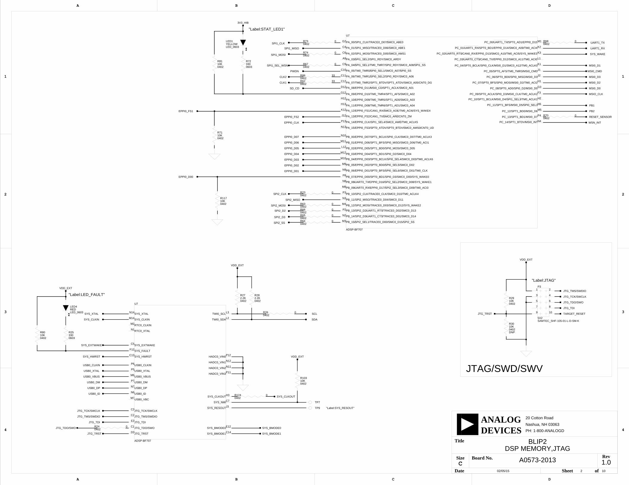
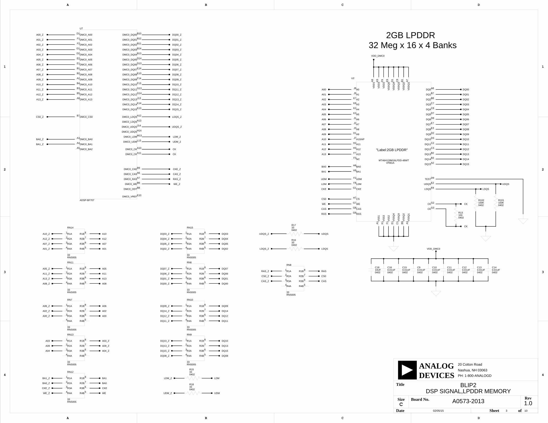
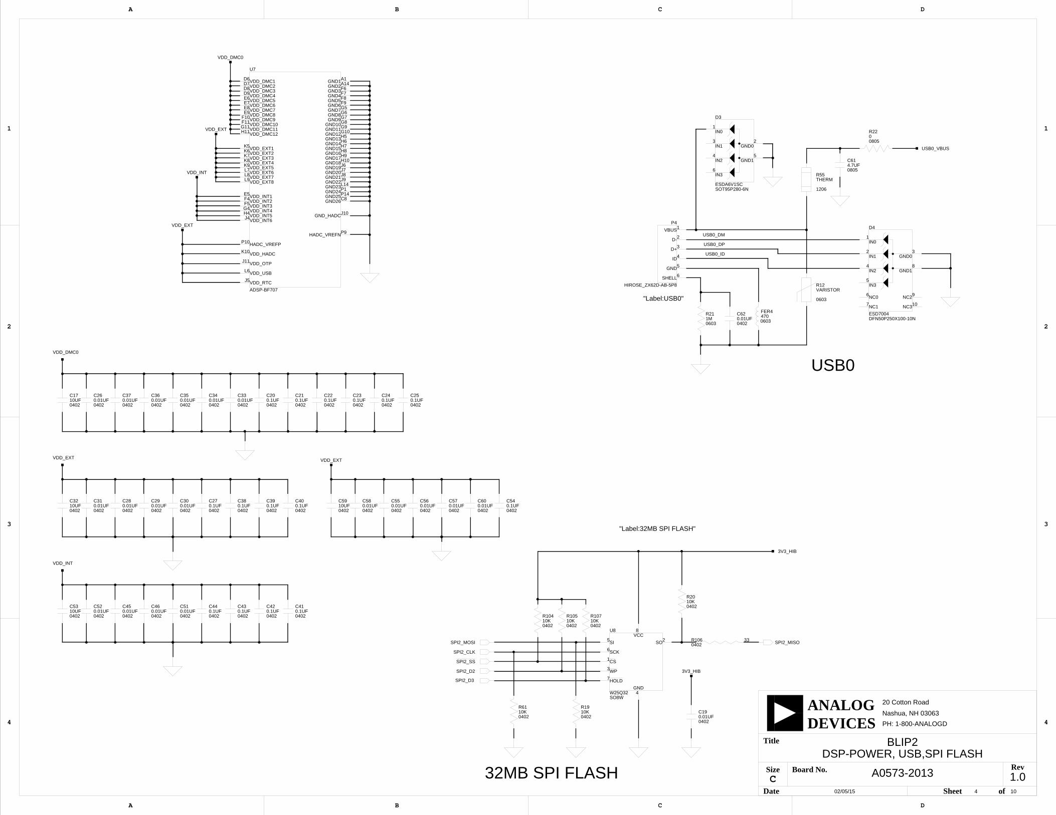
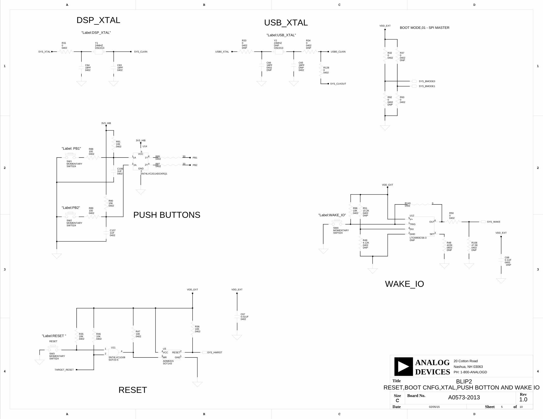
ADZS-BF707-BLIP2 BOARD SCHEMATIC
INDEX

Contents
viii ADZS-BF707-BLIP2 Board Evaluation System Manual

ADZS-BF707-BLIP2 Board Evaluation System Manual ix
PREFACE
Thank you for purchasing the ADZS-BF707-BLIP2 board, Analog Devices, Inc. low-cost evaluation system for the ADSP-BF70x family of Blackfin® processors.
The ADSP-BF707 processor is a member of the Blackfin family of prod-ucts. Blackfin processors combine a dual-MAC state-of-the-art signal processing engine, the advantages of a clean, orthogonal RISC-like micro-processor instruction set, and single-instruction, multiple-data (SIMD) multimedia capabilities into a single instruction-set architecture. New enhancements to the Blackfin+™ core add 32-bit MAC and 16-bit com-plex MAC support, cache enhancements, branch prediction and other instruction set improvements, all while maintaining instruction set com-patibility to previous Blackfin products.
The ADZS-BF707-BLIP2 board is shipped with all of the necessary hard-ware—you can start the evaluation immediately. The package contains the standalone evaluation board, CE-approved power supply, and USB cable. The BLIP2 board ships with an ICE-1000 emulator.
A RF Wireless connector is provided for connecting the BLIP2 board to an Analog Devices Wireless Sensor Network (WSN) cluster board (EV-ADRN-WSN-2Z).
The on-board mechanical switches are push buttons.
Product Overview
x ADZS-BF707-BLIP2 Board Evaluation System Manual
The evaluation board is designed to be used in conjunction with the CrossCore® Embedded Studio (CCES) development tools to test capabil-ities of the ADSP-BF70x processors. The development environment aids advanced application code development and debug, such as:
• Create, compile, assemble, and link application programs written in C++, C, and assembly
• Load, run, step, halt, and set breakpoints in application programs
• Read and write data and program memory
• Read and write core and peripheral registers
Product OverviewThe board features:
• Analog Devices ADSP-BF707 processor
• 184-ball BGA package
• 24 MHz crystal oscillator for processor
• 24 MHz crystal oscillator for USB
• Mobile DDR memory (DMC0) chip
• 32M bit x 16 x 4 banks (2G bit)
• MT46H128M16LFDD-48WT
• Quad SPI Flash (SPI2)
• 32M bit serial flash memory
• Windbond W25Q32
ADZS-BF707-BLIP2 Board Evaluation System Manual xi
Preface
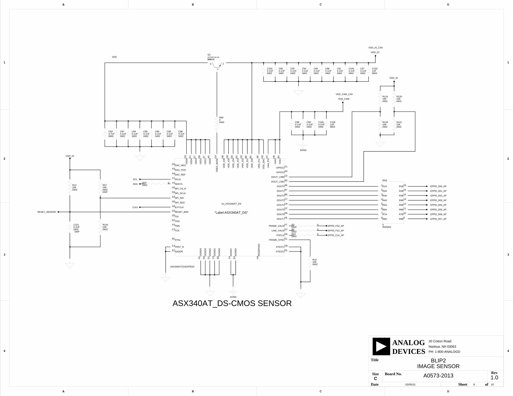
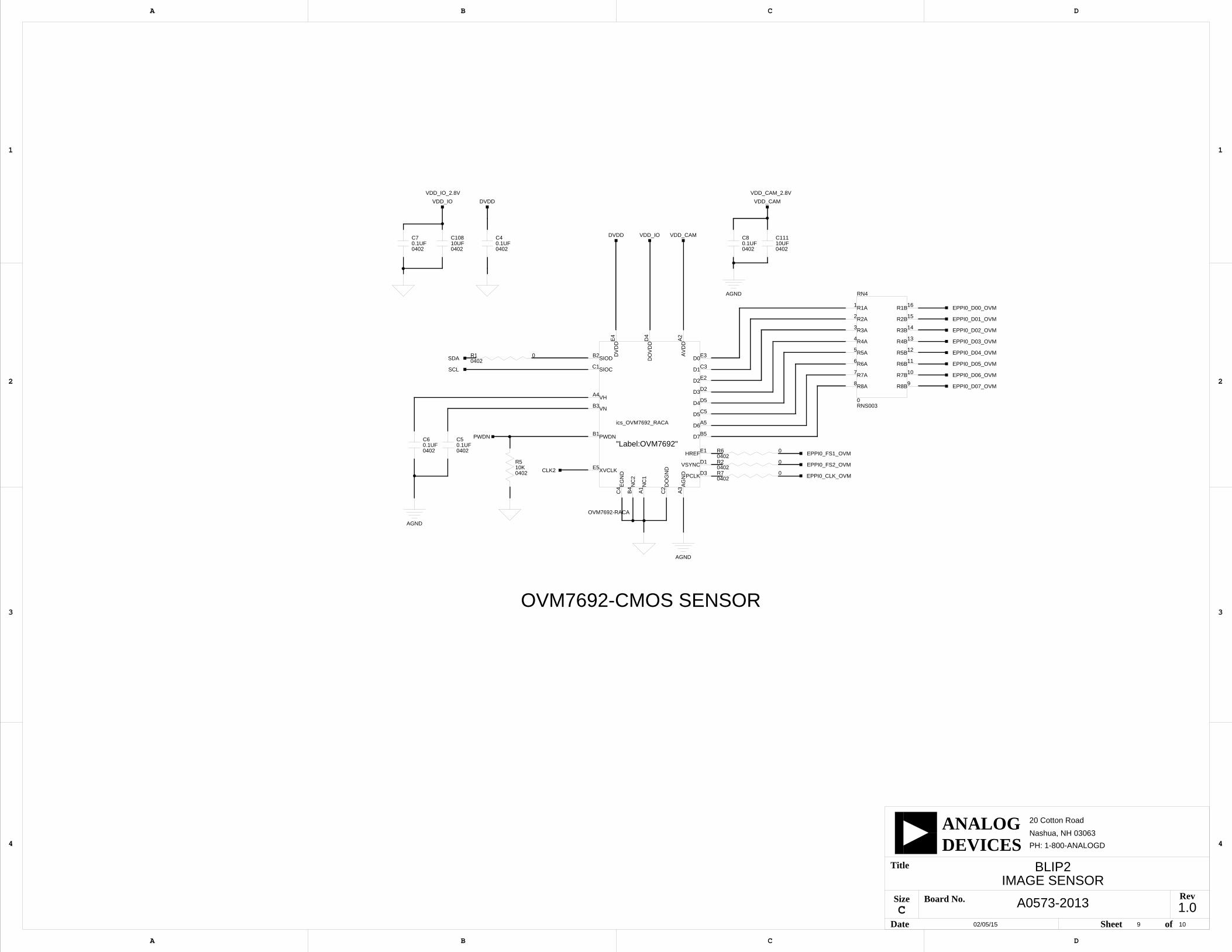
• CMOS imaging sensors
• ASX340AT by Aptina / ON Semiconductor and M12 lens holder
• OVM7692 camera module by Omnivision
• RF Wireless
• 4 x 2 connector
• 0.05” socket
• Universal Asynchronous Receiver/Transmitter (UART1)
• FTDI FT232RQ USB to UART converter
• USB Mini B connector
• USB interface
• Micro AB connector
• RESET controller
• Analog Devices ADM6315 microprocessor supervisory circuits
• Debug (JTAG/SWD/SWO) interface
• JTAG/SWD/SWO 10-pin 0.05” header for use with Analog Devices emulators
• LEDs
• Two LEDs: one board status (yellow), one SYS_FAULT (red)
• Push buttons
• Four push buttons: one reset, one wake I/O, and two GPIO
Purpose of This Manual
xii ADZS-BF707-BLIP2 Board Evaluation System Manual
• External power supply
• CE compliant
• 5V @ 3.6 amps
• Other features
• SD/MMC memory connector
• 0-ohm resistors for processor current measurement
For information about the hardware components of the BLIP2 board, refer to ADZS-BF707-BLIP2 Board Bill Of Materials.
Purpose of This ManualThe ADZS-BF707-BLIP2 Board Evaluation System Manual provides instructions for installing the product hardware (board). The text describes operation and configuration of the board components and pro-vides guidelines for running your own code on the ADZS-BF707-BLIP2 board. Finally, a schematic and a bill of materials are provided for reference.
Intended AudienceThe primary audience for this manual is a programmer who is familiar with Analog Devices processors. This manual assumes that the audience has a working knowledge of the appropriate processor architecture, instruction set, and C/C++ programming languages.
Programmers who are unfamiliar with Analog Devices processors can use this manual, but should supplement it with other texts (such as the ADSP-BF70x Blackfin+ Processor Hardware Reference and the ADSP-BF70x Blackfin+ Processor Programming Reference) that describe your target architecture.
ADZS-BF707-BLIP2 Board Evaluation System Manual xiii
Preface
Programmers who are unfamiliar with CrossCore Embedded Studio should refer to the CCES online help.
Manual ContentsThe manual consists of:
• Chapter 1, Using ADZS-BF707-BLIP2 BoardDescribes BLIP2 board functionality from a programmer’s perspec-tive and provides a simplified memory map of the processor.
• Chapter 2, ADZS-BF707-BLIP2 Board Hardware ReferenceProvides information about the BLIP2 board hardware components.
• Appendix A, ADZS-BF707-BLIP2 Board Bill Of MaterialsProvides a list of hardware components used to manufacture the BLIP2 board.
• Appendix B, ADZS-BF707-BLIP2 Board SchematicLists the resources for board-level debugging.
What’s New in This ManualThis is the first edition (Revision 1.0) of the ADZS-BF707-BLIP2 Board Evaluation System Manual.

Technical Support
xiv ADZS-BF707-BLIP2 Board Evaluation System Manual
Technical SupportYou can reach Analog Devices processors and DSP technical support in the following ways:
• Post your questions in the processors and DSP support community at EngineerZone®:http://ez.analog.com/community/dsp
• Submit your questions to technical support directly at:http://www.analog.com/support
• E-mail your questions about processors and processor applications to: [email protected] [email protected] (Greater China support)
• Contact your Analog Devices sales office or authorized distributor. Locate one at:www.analog.com/adi-sales
• Send questions by mail to:Processors and DSP Technical SupportAnalog Devices, Inc.Three Technology WayP.O. Box 9106Norwood, MA 02062-9106USA
Supported ProcessorsThis evaluation system supports Analog Devices ADSP-BF707 Blackfin processors.
ADZS-BF707-BLIP2 Board Evaluation System Manual xv
Preface
Supported ToolsInformation on supported tools for the ADZS-BF707-BLIP2 board and the ADSP-BF70x family of processors is:
http://www.analog.com/BLIP
Product InformationProduct information can be obtained from the Analog Devices Web site and the online help system.
Analog Devices Web SiteThe Analog Devices Web site, www.analog.com, provides information about a broad range of products—analog integrated circuits, amplifiers, converters, and digital signal processors.
To access a complete technical library for each processor family, go to http://www.analog.com/processors/technical_library. The manuals selection opens a list of current manuals related to the product as well as a link to the previous revisions of the manuals. When locating your manual title, note a possible errata check mark next to the title that leads to the current correction report against the manual.
Also note, myAnalog.com is a free feature of the Analog Devices Web site that allows customization of a Web page to display only the latest information about products you are interested in. You can choose to receive weekly e-mail notifications containing updates to the Web pages that meet your interests, including documentation errata against all manu-als. myAnalog.com provides access to books, application notes, data sheets, code examples, and more.
Notation Conventions
xvi ADZS-BF707-BLIP2 Board Evaluation System Manual
Visit myAnalog.com (found on the Analog Devices home page) to sign up. If you are a registered user, just log on. Your user name is your e-mail address.
EngineerZoneEngineerZone is a technical support forum from Analog Devices. It allows you direct access to ADI technical support engineers. You can search FAQs and technical information to get quick answers to your embedded processing and DSP design questions.
Use EngineerZone to connect with other DSP developers who face similar design challenges. You can also use this open forum to share knowledge and collaborate with the ADI support team and your peers. Visit http://ez.analog.com to sign up.
Notation ConventionsText conventions used in this manual are identified and described as follows.
Example Description
File > Close Titles in reference sections indicate the location of an item within the CCES environment’s menu system (for example, the Close command appears on the File menu).
{this | that} Alternative required items in syntax descriptions appear within curly brackets and separated by vertical bars; read the example as this or that. One or the other is required.
[this | that] Optional items in syntax descriptions appear within brackets and sepa-rated by vertical bars; read the example as an optional this or that.
[this,…] Optional item lists in syntax descriptions appear within brackets delim-ited by commas and terminated with an ellipse; read the example as an optional comma-separated list of this.
ADZS-BF707-BLIP2 Board Evaluation System Manual xvii
Preface
.SECTION Commands, directives, keywords, and feature names are in text with letter gothic font.
filename Non-keyword placeholders appear in text with italic style format.
Note: For correct operation, ...A Note provides supplementary information on a related topic. In the online version of this book, the word Note appears instead of this
symbol.
Caution: Incorrect device operation may result if ...Caution: Device damage may result if ... A Caution identifies conditions or inappropriate usage of the product that could lead to undesirable results or product damage. In the online version of this book, the word Caution appears instead of this symbol.
Warning: Injury to device users may result if ... A Warning identifies conditions or inappropriate usage of the product that could lead to conditions that are potentially hazardous for the devices users. In the online version of this book, the word Warning appears instead of this symbol.
Example Description
Notation Conventions
xviii ADZS-BF707-BLIP2 Board Evaluation System Manual
ADZS-BF707-BLIP2 Board Evaluation System Manual 1-1
1 USING ADZS-BF707-BLIP2 BOARD
This chapter provides information to assist you with development of pro-grams for the ADZS-BF707-BLIP2 evaluation system.
The following topics are covered.
• Package Contents
• Default Configuration
• BLIP2 Board Installation
• BLIP2 Board Session Startup
• Evaluation License
• Mobile DDR Memory
• SPI Flash
• UART1 Interface
• USB Interface
• SD Interface
• Debug Interface
• Power-On-Self Test
• RF Wireless Interface
• Power Architecture
Package Contents
1-2 ADZS-BF707-BLIP2 Board Evaluation System Manual
• Example Programs
• Reference Design Information
Package ContentsYour ADZS-BF707-BLIP2 board package contains the following items.
• ADZS-BF707-BLIP2 board
• ICE-1000 emulator
• Tripod
• M12 lens
• Universal 5V DC power
• USB Mini-B to Standard-A cable
• USB Micro-B to Standard-A cable
• Release note
Contact the vendor where you purchased your BLIP2 board or contact Analog Devices, Inc. if any item is missing.
Default ConfigurationThe ADZS-BF707-BLIP2 board is designed to run as a standalone unit.
When removing the BLIP2 board from the package, handle the board carefully to avoid the discharge of static electricity, which can damage some components.
ADZS-BF707-BLIP2 Board Evaluation System Manual 1-3
Using ADZS-BF707-BLIP2 Board
BLIP2 Board InstallationIt is assumed that the CrossCore Embedded Studio software is installed and running on your PC.
Follow these instructions to ensure correct operation of the product soft-ware and hardware.
Step 1: Connect an emulator to the BLIP2 board.
1. Plug one side of the included USB cable into the USB connector of the emulator. Plug the other side into a USB port of the PC.
2. The status LED (labeled STATUS) lights up yellow if the connection with the PC is working and the appropriate Windows driver is installed. Please refer to the appropriate emulator manual if the sta-tus LED does not turn on.
3. Attach the emulator header (J2) on the bottom of the ICE-1000 to the P3 connector on the BLIP2 board.
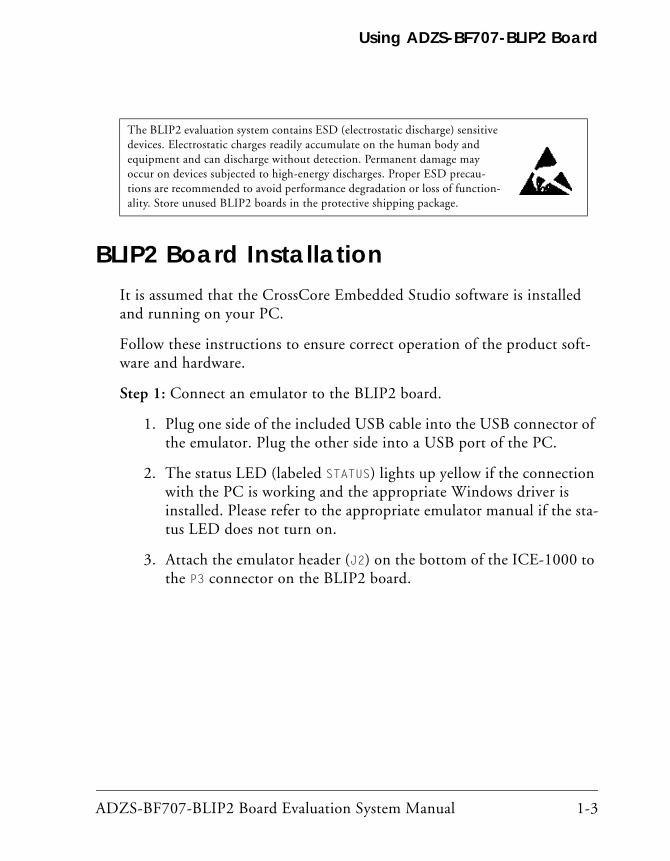
The BLIP2 evaluation system contains ESD (electrostatic discharge) sensitive devices. Electrostatic charges readily accumulate on the human body and equipment and can discharge without detection. Permanent damage may occur on devices subjected to high-energy discharges. Proper ESD precau-tions are recommended to avoid performance degradation or loss of function-ality. Store unused BLIP2 boards in the protective shipping package.
BLIP2 Board Session Startup
1-4 ADZS-BF707-BLIP2 Board Evaluation System Manual
Step 2: Providing power to the BLIP2 board.
1. Plug one side of the USB Micro-B to Standard-A cable into the USB connector P4 on the BLIP2 board. Plug the other side into a USB port of the PC. If there lacks a USB port to supply power to BLIP2 board, follow the instructions in the next two steps.
2. Plug the jack-end of the assembled power adaptor into the power connector (REFDES) P5 (labeled 5V) on the BLIP2 board.
3. Plug the other side of the power adaptor into a power outlet.
BLIP2 Board Session StartupIt is assumed that the CrossCore Embedded Studio software is installed and running on your PC.
Note: If you connect the board or emulator first (before installing CCES) to the PC, the Windows driver wizard may not find the board drivers.
1. Navigate to the CCES environment through the Start menu.
Note that CCES is not connected to the target board.
2. Use the Debug Configurations wizard to connect to the BLIP2 board.
If a debug configuration exists already, select the appropriate configuration and click Debug. Go to step 8.
ADZS-BF707-BLIP2 Board Evaluation System Manual 1-5
Using ADZS-BF707-BLIP2 Board
To create a debug configuration, do one of the following:
• Click the down arrow next to the bug icon , select Debug Configurations.
• Choose Run > Debug Configurations.
The Debug Configuration dialog box appears.
3. Select CrossCore Embedded Studio Application and click (New launch configuration).
The Select Processor page of the Session Wizard appears.
4. Ensure Blackfin is selected in Processor family. In Processor type, select ADSP-BF707. Click Next.
The Select Connection Type page of the Session Wizard appears.
5. Select Emulator and click Next.
The Select Platform page of the Session Wizard appears.
6. Choose the type of emulator that is connected to the BLIP2 board.
An ICE-1000 emulator is included in the package.
7. Click Finish to close the wizard.
The new debug configuration is created and added to the Debug Configurations list.
8. In the Name edit box, users can select an appropriate name to describe the configuration, otherwise a default name is provided.
9. Select the Custom Board Support tab and check the Enable cus-tomizations box. Click on Browse and select the ADZS-BF707-BLIP2-proc.xml file found in the ADZS_BF707_BLIP2_Board-Rel1.0.0\Blackfin\Examples folder.
Evaluation License
1-6 ADZS-BF707-BLIP2 Board Evaluation System Manual
Click OK. In the Run/Debug settings, click Apply to save and apply the changes.
10.In the Program(s) to load section, choose the program to load (if the appropriate program is not already populated) when connect-ing to the board. If not loading any program upon connection to the target, do not make any changes.
While connected to the target, there is no way to choose a program to download. To load a program once connected, terminate the session and then load the new program.
To delete a configuration, go to the Debug Configurations dialog box and select the configuration to delete. Click and choose Yes when asked if you wish to delete the selected launch configuration. Then Close the dialog box.
To disconnect from the target board, click the terminate button or choose Run > Terminate.
To delete a session, choose Target > Session > Session List. Select the session name from the list and click Delete. Click OK.
The default configurations that show up in the CCES Debug Con-figurations wizard are for JTAG mode debugging only. To use SWD mode, create a new platform using the Target Configurator.
Evaluation LicenseWhen starting CCES for the first time, you are prompted to install a license with a serial number or to enable evaluation of the product without a serial number. In the box that contains the EZ-Board is a business card with a serial number on it. When prompted, choose “I have a serial num-ber that I would like to activate” and enter the serial number shown on the card. If the evaluation license is installed but not activated, it allows
ADZS-BF707-BLIP2 Board Evaluation System Manual 1-7
Using ADZS-BF707-BLIP2 Board
10 days of unrestricted use and then becomes disabled. The license can be re-enabled by activation. Once activated, the evaluation license offers unrestricted use for a defined period and then becomes disabled until an additional license is installed.
If installing CCES without using a serial number, you will be lim-ited to 180 days.
An evaluation license can be upgraded to a full license. Licenses can be purchased from:
• Analog Devices directly. Call (800) 262-5645 or 781-937-2384 or go to: http://www.analog.com/buyonline.
• Analog Devices, Inc. local sales office or authorized distributor. To locate one, go to:www.analog.com/adi-sales.
Mobile DDR MemoryThe ADSP-BF707 processor connects to a 2Gb Micron MT46H128M16 chip through the Double Data Rate Synchronous Dynamic Ran-dom-Access Memory controller. The memory controller on the processor and the Mobile DDR memory chip are powered by the on-board 1.8V regulator. The memory controller on the processor can operate at a maxi-mum clock frequency of 200 MHz. Data is transferred between the processor and the memory chip on both the rising and falling edges of the clock.
With a CCES session running and connected to the BLIP2 board through an emulator, the memory controller registers are configured automatically each time the processor is reset through a soft reset using CCES. The val-ues are used whenever mobile DDR chip is accessed through the debugger (for example, when viewing memory or loading a program).
SPI Flash
1-8 ADZS-BF707-BLIP2 Board Evaluation System Manual
To disable the automatic setting of the memory controller registers, select Target Options from the Session menu in CCES and uncheck Use XML reset values.
SPI FlashThe ADSP-BF707 processor has three SPI interfaces: SPI0, SPI1, and SPI2. SPI2 is connected to a Winbond W25Q32BC 32 Mb serial flash memory with quad SPI support. This flash is used for booting and scratchpad space.
UART1 InterfaceThe ADSP-BF707 processor has two built-in universal asynchronous transmitters (UARTs). UART1 is connected to an FTDI, FT232RQ, USB to UART converter IC (U15).
For more information, refer to the UART1 example, which is included in the ADZS-BF707-BLIP2 Board Support Package.
USB InterfaceThe ADSP-BF707 processor has an integrated USB PHY; the BLIP2 board provides a micro AB connector. The board supports USB high speed mode.
To learn about the device and host modes of the processor, refer to the USB example, which is included in the ADZS-BF707-BLIP2 Board Sup-port Package. For more information, refer to the ADSP-BF70x Blackfin+ Processor Hardware Reference.
ADZS-BF707-BLIP2 Board Evaluation System Manual 1-9
Using ADZS-BF707-BLIP2 Board
SD InterfaceThe ADSP-BF707 processor has a secure digital (SD) interface that con-sists of a clock pin, command pin, card detect pin, and an 8-bit data bus.
Debug InterfaceThe BLIP2 board provides a JTAG/SWD/SWO connection through a connector (P3), which is a 0.05” pitch header. A 8-bit trace connection also is available through a connector (P2), although this is not supported at this time. See JTAG/SWD/SWO Connector (P3) for more information.
Power-On-Self TestThe Power-On-Self-Test Program (POST) tests all BLIP2 board peripher-als, except for SD card interface, and validates functionality as well as connectivity to the processor. Once assembled, each BLIP2 board is fully tested for an extended period of time with POST. All BLIP2 boards are shipped with Video Occupancy Sensor real-time applications burned into flash memory. For executing POST code, refer to the Power_On_Self_Test example in the Board Support Package.
Note that the source code for the POST program is included in the ADZS-BF707-BLIP2 Board Support Package along with the readme.txt file that describes how the board is configured to run POST.
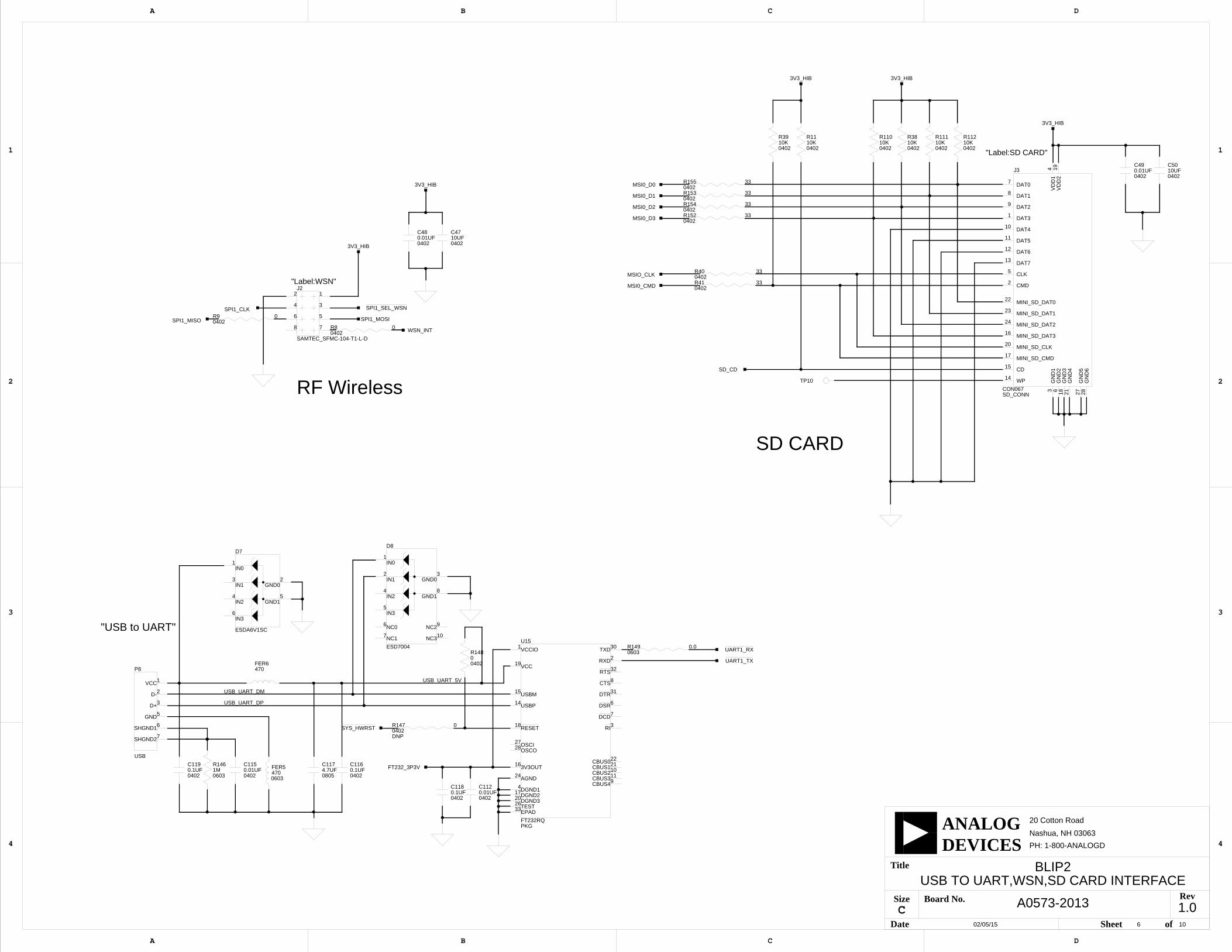
RF Wireless InterfaceA RF Wireless connector allows the BLIP2 board to be connected to an Analog Devices Inc. Wireless Sensor Network (WSN) cluster board EV-ADRN-WSN-2Z. Alternatively, it can be used as a general-purpose
Power Architecture
1-10 ADZS-BF707-BLIP2 Board Evaluation System Manual
connector for the SPI1 port, 3.2V supply, and ground. Note that any SPI1 pin can also be configured as GPIO. For pinout information, go to ADZS-BF707-BLIP2 Board Schematic.
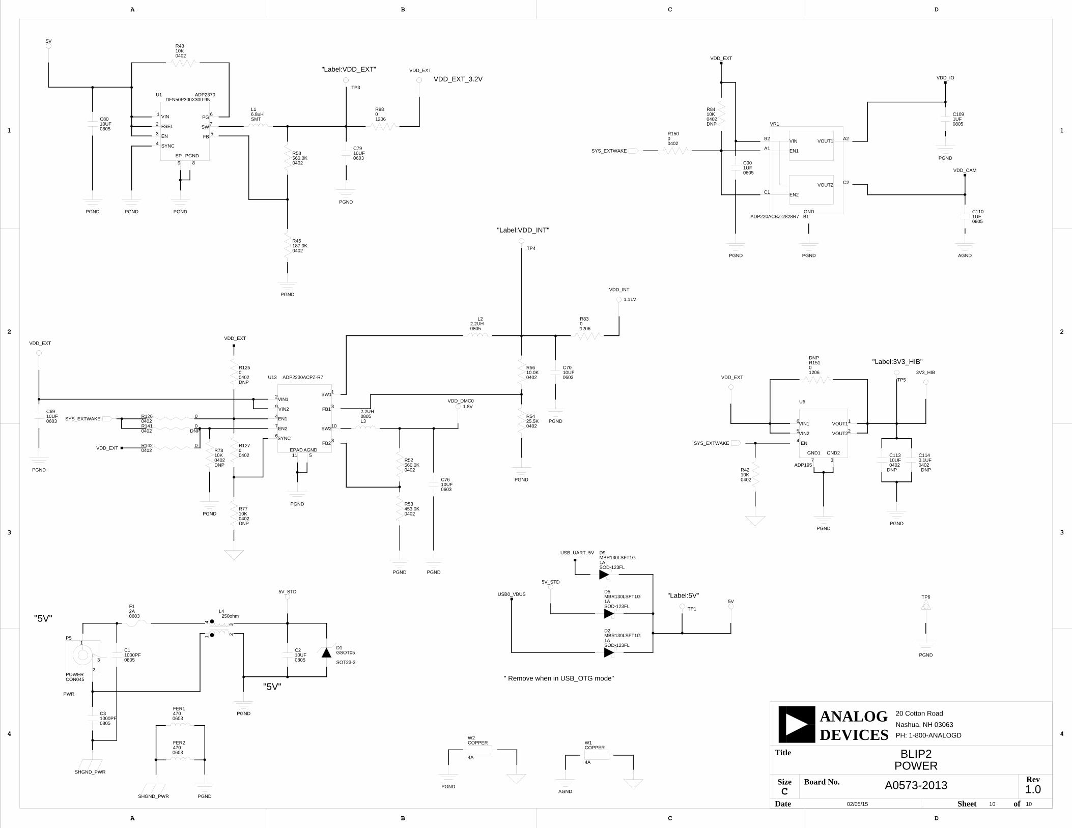
Power ArchitectureThe ADZS-BF707-BLIP2 board has three primary voltage domains: 3.2V, 1.1V, and 1.8V. The power input is a 5V wall adaptor.
The Analog Devices ADP2370 voltage regulator provides 3.2V for the VDD_EXT signal and the 3.2V power requirements of the board. The ADP2230 voltage regulator provides 1.1V for the VDD_INT signal in addi-tion to providing 1.8V for the VDD_DMCO signal. The ADP195 load switch is used to create a collapsible power domain to save power during hiber-nate mode. The ADP220 voltage regulator provides 2.8V to the CMOS imaging sensors.
Example ProgramsExample programs are provided with the ADZS-BF707-BLIP2 Board Support Package to demonstrate various capabilities of the product. The programs can be found in the ADZS_BF707_BLIP2_Board-Rel1.0.0\Black-fin\Examples folder. The number after the “Rel” could be higher for newer versions. Refer to a readme file provided with each example for more information.
ADZS-BF707-BLIP2 Board Evaluation System Manual 1-11
Using ADZS-BF707-BLIP2 Board
Reference Design InformationA reference design info package is available for download on the Analog Devices Web site. The package provides information on the design, lay-out, fabrication, and assembly of the BLIP2 board.
The information can be found at:
http://www.analog.com/BLIP
Reference Design Information
1-12 ADZS-BF707-BLIP2 Board Evaluation System Manual
ADZS-BF707-BLIP2 Board Evaluation System Manual 2-1
2 ADZS-BF707-BLIP2 BOARD HARDWARE REFERENCE
This chapter describes the hardware design of the ADZS-BF707-BLIP2 board.
The following topics are covered.
• System ArchitectureDescribes the board’s configuration and explains how the board components interface with the processor.
• Push ButtonsShows the locations and describes the push buttons.
• LEDsShows the locations and describes the LEDs.
• ConnectorsShows the locations and provides part numbers for the on-board connectors. In addition, the manufacturer and part number infor-mation is provided for the mating parts.
System Architecture
2-2 ADZS-BF707-BLIP2 Board Evaluation System Manual
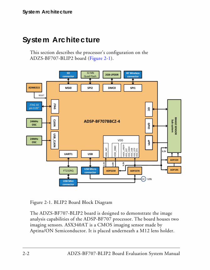
System ArchitectureThis section describes the processor’s configuration on the ADZS-BF707-BLIP2 board (Figure 2-1).
The ADZS-BF707-BLIP2 board is designed to demonstrate the image analysis capabilities of the ADSP-BF707 processor. The board houses two imaging sensors. ASX340AT is a CMOS imaging sensor made by Aptina/ON Semiconductor. It is placed underneath a M12 lens holder.
Figure 2-1. BLIP2 Board Block Diagram
ADSP-BF707BBCZ-4
JTAG
CLKIN
SPI2
32 Mb Quad Flash
USB
USB Microconnector
JTAG 10 pin 0.05”
DMC0
2GB-LPDDR
VDD_
EXT
VDD_
HADC
VDD_
USB
VDD_
RTC
VDD_
INT
VDD_
DMC
DC VIN
ePPIG
PIOI2C
IMAG
E SENSO
RSub system
SPI1
RF Wirelessconnector
24MHz OSC
VDD_
OTP
MSI0
SD connector
ADP2370
1.1V
1.8V
3.2V
ADM6315
RESET
ADP220
3.2V
USB_CLKIN
24MHz OSC
ADP195
HADC
_VRE
FP
VDD
UART1
USB Miniconnector
FT232RQ ADP2230
ADZS-BF707-BLIP2 Board Evaluation System Manual 2-3
ADZS-BF707-BLIP2 Board Hardware Reference
OVM7692 is a camera module made by Omnivision. It packages an OV7692 imaging sensor with a lens.
The ADZS-BF707-BLIP2 board has a 24 MHz input clock and runs at 384 MHz internally.
USB circuitry and a micro USB AB connector enable the BLIP2 board to connect to a host. The clock for the USB circuit is generated by a 24 MHz oscillator.
An FT232RQ device from Future Technology Devices International and a USB Mini-B connector allow the UART1 port of the ADSP-BF707 pro-cessor to connect to a USB port of a host.
The SD connector enables plug-in of an SD card or a WiFi module that supports SD card interface.
The RF Wireless connector allows the connection of the BLIP2 board to an Analog Devices Inc. Wireless Sensor Network (WSN) Cluster Board. Alternatively, it can be used as a general-purpose connector for the SPI1 port, 3.2V supply, and ground. Note that any SPI1 pin can also be config-ured as GPIO.
See ADZS-BF707-BLIP2 Board Schematic and the Wireless Sensor Net-work (WSN) cluster board EV-ADRN-WSN-2ZWSN for more information.
Push Buttons
2-4 ADZS-BF707-BLIP2 Board Evaluation System Manual
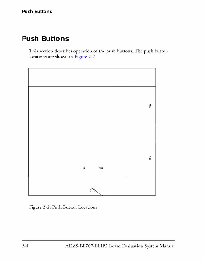
Push ButtonsThis section describes operation of the push buttons. The push button locations are shown in Figure 2-2.
Figure 2-2. Push Button Locations
ADZS-BF707-BLIP2 Board Evaluation System Manual 2-5
ADZS-BF707-BLIP2 Board Hardware Reference
GPIO Push Buttons (SW1 and SW2)The GPIO push buttons (SW1 and SW2) are connected to the processor’s signals PC_11/SPT1_BFS/MSI0_D5/SPI0_SEL3 and PC_12/SPT1_BD0/MSI0_D6, respectively. The signals are used for debugging purposes.
Reset Push Button (SW3)The reset push button (SW3) resets the following ICs: processor (U7)and the USB to UART converter (U15).
WAKE IO Push Button (SW4)The WAKE IO push button (SW4) wakes up the processor after it goes into hibernate mode.
LEDs
2-6 ADZS-BF707-BLIP2 Board Evaluation System Manual
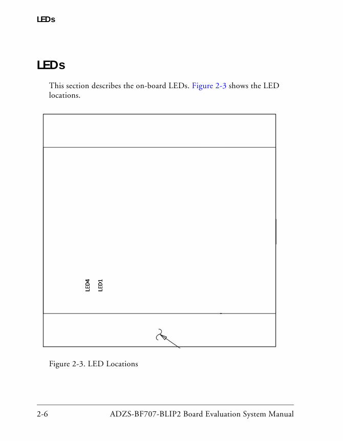
LEDsThis section describes the on-board LEDs. Figure 2-3 shows the LED locations.
Figure 2-3. LED Locations
ADZS-BF707-BLIP2 Board Evaluation System Manual 2-7
ADZS-BF707-BLIP2 Board Hardware Reference
GPIO Status LED (LED1)When GPIO Status LED (LED1) (yellow) is ON, it indicates the status of the board.
SYS_FAULT LED (LED4)When the SYS_FAULT LED (LED4) (red) is ON, it indicates a system fault. For more information, refer to the ADSP-BF70x Blackfin+ Processor Hard-ware Reference.
Connectors
2-8 ADZS-BF707-BLIP2 Board Evaluation System Manual
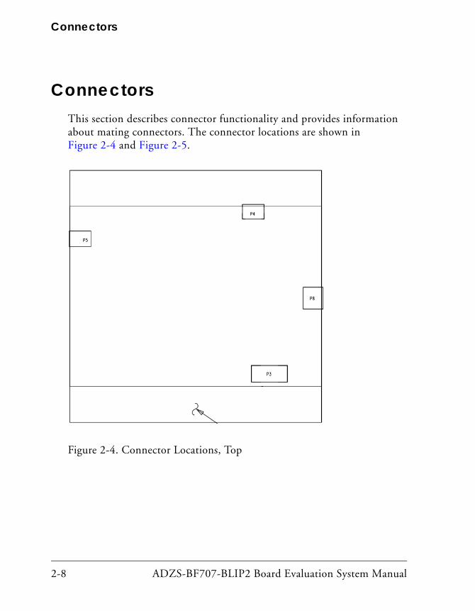
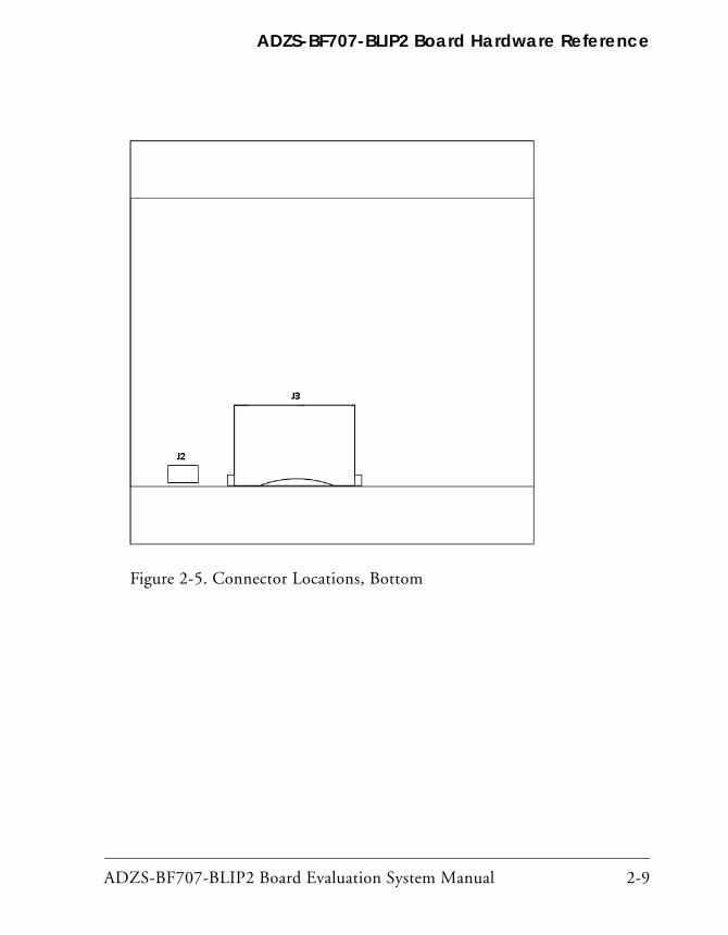
ConnectorsThis section describes connector functionality and provides information about mating connectors. The connector locations are shown in Figure 2-4 and Figure 2-5.
Figure 2-4. Connector Locations, Top
ADZS-BF707-BLIP2 Board Evaluation System Manual 2-9
ADZS-BF707-BLIP2 Board Hardware Reference
Figure 2-5. Connector Locations, Bottom
Connectors
2-10 ADZS-BF707-BLIP2 Board Evaluation System Manual
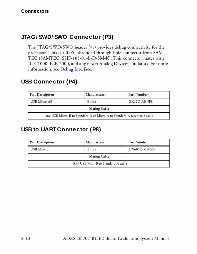
JTAG/SWD/SWO Connector (P3)The JTAG/SWD/SWO header (P3) provides debug connectivity for the processor. This is a 0.05” shrouded through-hole connector from SAM-TEC (SAMTEC_SHF-105-01-L-D-SM-K). This connector mates with ICE-1000, ICE-2000, and any newer Analog Devices emulators. For more information, see Debug Interface.
USB Connector (P4)
USB to UART Connector (P8)
Part Description Manufacturer Part Number
USB Micro-AB Hirose ZX62D-AB-5P8
Mating Cable
Any USB Micro-B to Standard-A or Micro-A to Standard-A receptacle cable
Part Description Manufacturer Part Number
USB Mini-B Hirose UX60SC-MB-5S8
Mating Cable
Any USB Mini-B to Standard-A cable
ADZS-BF707-BLIP2 Board Evaluation System Manual 2-11
ADZS-BF707-BLIP2 Board Hardware Reference
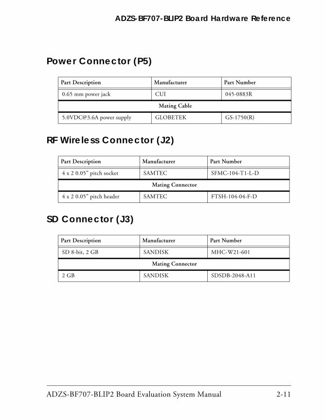
Power Connector (P5)
RF Wireless Connector (J2)
SD Connector (J3)
Part Description Manufacturer Part Number
0.65 mm power jack CUI 045-0883R
Mating Cable
[email protected] power supply GLOBETEK GS-1750(R)
Part Description Manufacturer Part Number
4 x 2 0.05” pitch socket SAMTEC SFMC-104-T1-L-D
Mating Connector
4 x 2 0.05” pitch header SAMTEC FTSH-104-04-F-D
Part Description Manufacturer Part Number
SD 8-bit, 2 GB SANDISK MHC-W21-601
Mating Connector
2 GB SANDISK SDSDB-2048-A11
Connectors
2-12 ADZS-BF707-BLIP2 Board Evaluation System Manual
ADZS-BF707-BLIP2 Board Evaluation System Manual A-1
A ADZS-BF707-BLIP2 BOARD BILL OF MATERIALS
The bill of materials corresponds to ADZS-BF707-BLIP2 Board Schematic.
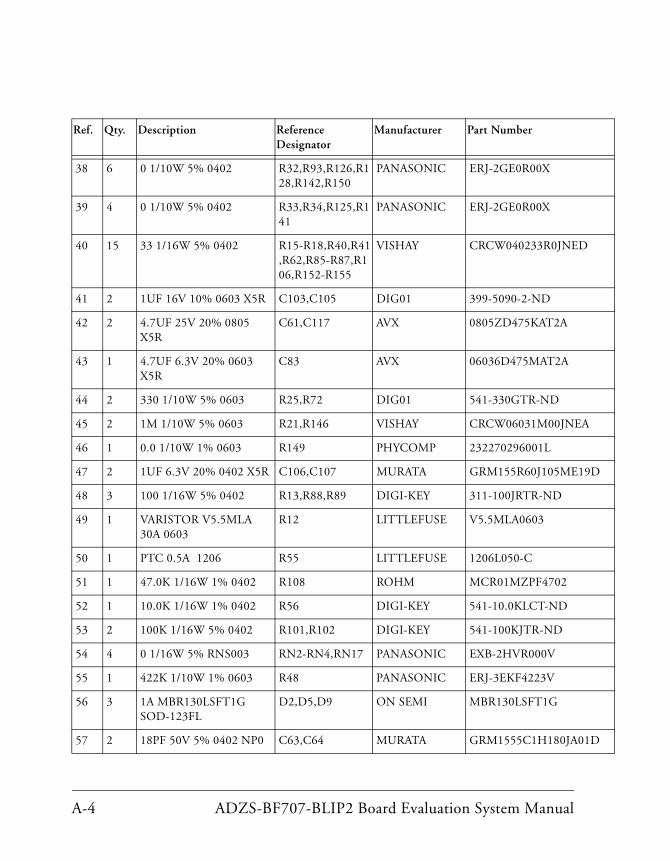
Ref. Qty. Description Reference Designator
Manufacturer Part Number
1 1 SN74LVC1G08 SOT23-5 U11 TI SN74LVC1G08DBVE
2 1 24MHZ OSC013 Y1 DIGI-KEY 535-9138-2-ND
3 1 24MHZ OSC013 Y2 DIGI-KEY 535-9138-2-ND
4 1 W25Q32 SO8W U8 WINBOND W25Q32FVSSIG
5 1 FT232RQ QFN50P500X500-33NA
U15 DIGI-KEY 768-1008-1-ND
6 1 ADP2230 DFN50P300X300-11N
U13 ANALOG DEVICES
ADP2230
7 1 ADP2370ACPZ-R7 DFN50P300X300-9N
U1 ANALOG DEVICES
ADP2370ACPZ-R7
8 1 LTC6993CS6-3 SOT95P280-6N
U12 LINEAR TECH LTC6993CS6-3#TRMPBF
9 1 OVM7692-RACA BGA25C50X54P5X5_282X318
U4 OMNIVISION TECH
OVM7692-RACA
10 1 SN74LVC2G14DCKRQ1 SOT65P210-6N
U14 DIGI-KEY 296-13011-1-ND
11 1 ASX340AT2C00XPED0 BGA63C65P8X8_7500X7500_SCKT
U10 APTINA ASX340AT2C00XPED0
A-2 ADZS-BF707-BLIP2 Board Evaluation System Manual
12 1 ADP195 DFN65P200X200-7N
U5 ANALOG DEVICES
ADP195ACPZ-R7
13 1 ADM6315 SOT143 U3 ANALOG DEVICES
ADM6315-29D2ARTZR7
14 1 ADP220ACBZ-2828R7 BGA6C50P2X3_100X150
VR1 ANALOG DEVICES
ADP220ACBZ-2828R7
15 1 ADSP-BF707 BGA184C80P14X14_1200X1200_SCKT
U7 ANALOG DEVICES
ADSP-BF707BBCZ-4
16 1 PWR .65MM CON045 P5 DIGI-KEY CP1-023-ND
17 2 MOMENTARY SWT024 SW3,SW4 PANASONIC EVQ-Q2K03W
18 2 MOMENTARY SWT024 SW1,SW2 PANASONIC EVQ-Q2K03W
19 1 SD_CONN 8-BIT CON067
J3 MORETHA-NALL
MHC-W21-601-LF
20 1 USB 5PIN CON069 P8 DIGI-KEY H11589CT-ND
21 1 USB-MICRO 5PIN HIROSE_ZX62D-AB-5P8
P4 DIGI-KEY H11494CT-ND
22 1 0.05 10PIN SAM-TEC_SHF-105-01-L-D-SM-K
P3 SAMTEC SHF-105-01-L-D-SM-K-TR
23 1 IDC 4x2 SAMTEC_S-FMC-104-T1-L-D
J2 SAMTEC SFMC-104-T1-L-D
24 1 2A FAST 0603 F1 BOURNS INC SF-0603F200-2
25 1 0 1/4W 5% 1206 R151 KOA 0.0ECTRk7372BTTED
26 2 0 1/4W 5% 1206 R83,R98 KOA 0.0ECTRk7372BTTED
27 3 1UF 16V 10% 0805 X7R C90,C109,C110 DIGI-KEY 399-1284-2-ND
28 1 0 1/8W 5% 0805 R22 VISHAY CRCW08050000Z0EA
29 2 2.2UH 10% 0805 L2,L3 DIGI-KEY 490-1119-2-ND
Ref. Qty. Description Reference Designator
Manufacturer Part Number
ADZS-BF707-BLIP2 Board Evaluation System Manual A-3
ADZS-BF707-BLIP2 Board Bill Of Materials
30 2 1000PF 50V 10% 0805 X7R
C1,C3 DIGI-KEY 311-1136-2-ND
31 3 0.1UF 10V 10% 0402 X5R
C68,C101,C114 AVX 0402ZD104KAT2A
32 41 0.1UF 10V 10% 0402 X5R
C4-C8,C20-C25,C27,C38-C44,C54,C84-C89,C91-C100,C102,C104,C116,C118,C119
AVX 0402ZD104KAT2A
33 34 0.01UF 16V 10% 0402 X7R
C9-C16,C19,C26,C28-C31,C33-C37,C45,C46,C48,C49,C51,C52,C55-C58,C60,C62,C67,C112,C115
AVX 0402YC103KAT2A
34 35 10K 1/16W 5% 0402 R5,R10,R11,R14,R19,R20,R29,R35,R36,R38,R39,R42,R43,R46,R47,R61,R71,R80,R81,R90,R91,R96,R103-R105,R107,R110-R112,R117-R121,R143
VISHAY CRCW040210K0FKED
35 5 10K 1/16W 5% 0402 R30,R57,R77,R78,R84
VISHAY CRCW040210K0FKED
36 3 0 1/10W 5% 0402 R37,R92,R147 PANASONIC ERJ-2GE0R00X
37 35 0 1/10W 5% 0402 R1-R4,R6-R9,R23,R24,R26,R31,R44,R50,R60,R63-R68,R70,R73,R74,R79,R124,R127,R129-R131,R136-R138,R140,R148
PANASONIC ERJ-2GE0R00X
Ref. Qty. Description Reference Designator
Manufacturer Part Number
A-4 ADZS-BF707-BLIP2 Board Evaluation System Manual
38 6 0 1/10W 5% 0402 R32,R93,R126,R128,R142,R150
PANASONIC ERJ-2GE0R00X
39 4 0 1/10W 5% 0402 R33,R34,R125,R141
PANASONIC ERJ-2GE0R00X
40 15 33 1/16W 5% 0402 R15-R18,R40,R41,R62,R85-R87,R106,R152-R155
VISHAY CRCW040233R0JNED
41 2 1UF 16V 10% 0603 X5R C103,C105 DIG01 399-5090-2-ND
42 2 4.7UF 25V 20% 0805 X5R
C61,C117 AVX 0805ZD475KAT2A
43 1 4.7UF 6.3V 20% 0603 X5R
C83 AVX 06036D475MAT2A
44 2 330 1/10W 5% 0603 R25,R72 DIG01 541-330GTR-ND
45 2 1M 1/10W 5% 0603 R21,R146 VISHAY CRCW06031M00JNEA
46 1 0.0 1/10W 1% 0603 R149 PHYCOMP 232270296001L
47 2 1UF 6.3V 20% 0402 X5R C106,C107 MURATA GRM155R60J105ME19D
48 3 100 1/16W 5% 0402 R13,R88,R89 DIGI-KEY 311-100JRTR-ND
49 1 VARISTOR V5.5MLA 30A 0603
R12 LITTLEFUSE V5.5MLA0603
50 1 PTC 0.5A 1206 R55 LITTLEFUSE 1206L050-C
51 1 47.0K 1/16W 1% 0402 R108 ROHM MCR01MZPF4702
52 1 10.0K 1/16W 1% 0402 R56 DIGI-KEY 541-10.0KLCT-ND
53 2 100K 1/16W 5% 0402 R101,R102 DIGI-KEY 541-100KJTR-ND
54 4 0 1/16W 5% RNS003 RN2-RN4,RN17 PANASONIC EXB-2HVR000V
55 1 422K 1/10W 1% 0603 R48 PANASONIC ERJ-3EKF4223V
56 3 1A MBR130LSFT1G SOD-123FL
D2,D5,D9 ON SEMI MBR130LSFT1G
57 2 18PF 50V 5% 0402 NP0 C63,C64 MURATA GRM1555C1H180JA01D
Ref. Qty. Description Reference Designator
Manufacturer Part Number
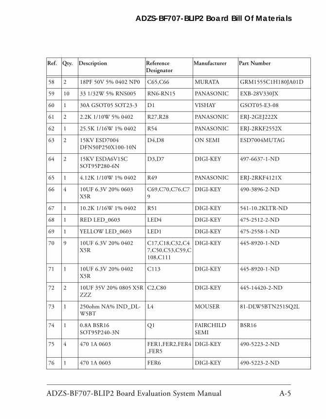
ADZS-BF707-BLIP2 Board Evaluation System Manual A-5
ADZS-BF707-BLIP2 Board Bill Of Materials
58 2 18PF 50V 5% 0402 NP0 C65,C66 MURATA GRM1555C1H180JA01D
59 10 33 1/32W 5% RNS005 RN6-RN15 PANASONIC EXB-28V330JX
60 1 30A GSOT05 SOT23-3 D1 VISHAY GSOT05-E3-08
61 2 2.2K 1/10W 5% 0402 R27,R28 PANASONIC ERJ-2GEJ222X
62 1 25.5K 1/16W 1% 0402 R54 PANASONIC ERJ-2RKF2552X
63 2 15KV ESD7004 DFN50P250X100-10N
D4,D8 ON SEMI ESD7004MUTAG
64 2 15KV ESDA6V1SC SOT95P280-6N
D3,D7 DIGI-KEY 497-6637-1-ND
65 1 4.12K 1/10W 1% 0402 R49 PANASONIC ERJ-2RKF4121X
66 4 10UF 6.3V 20% 0603 X5R
C69,C70,C76,C79
DIGI-KEY 490-3896-2-ND
67 1 10.2K 1/16W 1% 0402 R51 DIGI-KEY 541-10.2KLTR-ND
68 1 RED LED_0603 LED4 DIGI-KEY 475-2512-2-ND
69 1 YELLOW LED_0603 LED1 DIGI-KEY 475-2558-1-ND
70 9 10UF 6.3V 20% 0402 X5R
C17,C18,C32,C47,C50,C53,C59,C108,C111
DIGI-KEY 445-8920-1-ND
71 1 10UF 6.3V 20% 0402 X5R
C113 DIGI-KEY 445-8920-1-ND
72 2 10UF 35V 20% 0805 X5R ZZZ
C2,C80 DIGI-KEY 445-14420-2-ND
73 1 250ohm NA% IND_DL-W5BT
L4 MOUSER 81-DLW5BTN251SQ2L
74 1 0.8A BSR16 SOT95P240-3N
Q1 FAIRCHILD SEMI
BSR16
75 4 470 1A 0603 FER1,FER2,FER4,FER5
DIGI-KEY 490-5223-2-ND
76 1 470 1A 0603 FER6 DIGI-KEY 490-5223-2-ND
Ref. Qty. Description Reference Designator
Manufacturer Part Number
A-6 ADZS-BF707-BLIP2 Board Evaluation System Manual
77 1 187.0K 1/16W 1% 0402 R45 DIGI-KEY 311-187KLRTR-ND
78 2 560.0K 1/10W 1% 0402 R52,R58 PANASONIC ERJ-2RKF5603X
79 1 453.0K 1/10W 1% 0402 R53 PANASONIC ERJ-2RKF4533X
80 1 6.8uH 20% SMT L1 COILCRAFT XAL4030-682MEC
81 1 2GB LPDDR U2 MICRON MT46H128M16LFDD-48WT
Ref. Qty. Description Reference Designator
Manufacturer Part Number
D
4
3
2
1
A B C
20 Cotton Road
Nashua, NH 03063
A B C D
4
3
2
1
PH: 1-800-ANALOGD
C
Title
Size Board No.
Date Sheet of
DEVICESANALOG
Rev
BLIP2
A0573-2013
10
1.0
@PRINTORDER=1
102/05/15
BLIP2SCHEMATIC
0603330R25
JTG_TCK/SWCLK
JTG_TDI
JTG_TDO/SWO
JTG_TMS/SWDIO
JTG_TRST
USB0_CLKIN
USB0_DM
USB0_DP
USB0_ID
USB0_VBC
USB0_VBUS
USB0_XTAL
SYS_XTAL
HADC0_VIN0
HADC0_VIN1
HADC0_VIN2
HADC0_VIN3
TWI0_SCL
TWI0_SDA
RTC0_CLKIN
RTC0_XTAL
SYS_CLKIN
SYS_CLKOUT
SYS_BMODE0
SYS_BMODE1
SYS_EXTWAKE
SYS_FAULT
SYS_HWRST
SYS_NMI
SYS_RESOUT
U7
ADSP-BF707
J3
C7
C13
F12
C5
C14
E12
H3
M14
N1
M2
L2
L3
P11
N11
N12
P12
N14
P5
M6
M7
N6
N7
P7
P6
D3
C2
C1
E3
C3
D
4
3
2
1
A B C
20 Cotton Road
Nashua, NH 03063
A B C D
4
3
2
1
PH: 1-800-ANALOGD
C
Title
Size Board No.
Date Sheet of
DEVICESANALOG
Rev1.0
2 10
A0573-2013
BLIP2DSP MEMORY,JTAG
02/05/15
@PRINTORDER=2
DNP040210KR30
TP7
TP9
R124 00402
R23 00402
PA_00/SPI1_CLK/TRACE0_D07/SMC0_ABE0
PA_01/SPI1_MISO/TRACE0_D06/SMC0_ABE1
PA_02/SPI1_MOSI/TRACE0_D05/SMC0_AMS1
PA_03/SPI1_SEL2/SPI1_RDY/SMC0_ARDY
PA_04/SPI1_SEL1/TM0_TMR7/SPI2_RDY/SMC0_A08/SPI1_SS
PA_05/TM0_TMR0/SPI0_SEL1/SMC0_A07/SPI0_SS
PA_06/TM0_TMR1/SPI0_SEL2/SPI0_RDY/SMC0_A06
PA_07/TM0_TMR2/SPT1_BTDV/SPT1_ATDV/SMC0_A05/CNT0_DG
PB_08/UART0_TX/EPPI0_D16/SPI2_SEL2/SMC0_D08/SYS_WAKE1
PB_09/UART0_RX/EPPI0_D17/SPI2_SEL3/SMC0_D09/TM0_ACI3
PB_10/SPI2_CLK/TRACE0_CLK/SMC0_D10/TM0_ACLK4
PB_11/SPI2_MISO/TRACE0_D04/SMC0_D11
PB_12/SPI2_MOSI/TRACE0_D03/SMC0_D12/SYS_WAKE2
PB_13/SPI2_D2/UART1_RTS/TRACE0_D02/SMC0_D13
PB_14/SPI2_D3/UART1_CTS/TRACE0_D01/SMC0_D14
PB_15/SPI2_SEL1/TRACE0_D00/SMC0_D15/SPI2_SS
PA_08/EPPI0_D11/MSI0_CD/SPT1_ACLK/SMC0_A01
PA_09/EPPI0_D10/TM0_TMR4/SPT1_AFS/SMC0_A02
PA_10/EPPI0_D09/TM0_TMR5/SPT1_AD0/SMC0_A03
PA_11/EPPI0_D08/TM0_TMR6/SPT1_AD1/SMC0_A04
PA_12/EPPI0_FS1/CAN1_RX/SMC0_AOE/TM0_ACI6/SYS_WAKE4
PA_13/EPPI0_FS2/CAN1_TX/SMC0_ARE/CNT0_ZM
PA_14/EPPI0_CLK/SPI1_SEL4/SMC0_AWE/TM0_ACLK5
PA_15/EPPI0_FS3/SPT0_ATDV/SPT0_BTDV/SMC0_AMS0/CNT0_UD
PB_00/EPPI0_D07/SPT1_BCLK/SPI0_CLK/SMC0_D07/TM0_ACLK3
PB_01/EPPI0_D06/SPT1_BFS/SPI0_MISO/SMC0_D06/TM0_ACI1
PB_02/EPPI0_D05/SPT1_BD0/SPI0_MOSI/SMC0_D05
PB_03/EPPI0_D04/SPT1_BD1/SPI0_D2/SMC0_D04
PB_04/EPPI0_D03/SPT0_BCLK/SPI0_SEL4/SMC0_D03/TM0_ACLK6
PB_05/EPPI0_D02/SPT0_BD0/SPI0_SEL5/SMC0_D02
PB_06/EPPI0_D01/SPT0_BFS/SPI0_SEL6/SMC0_D01/TM0_CLK
PB_07/EPPI0_D00/SPT0_BD1/SPI0_D3/SMC0_D00/SYS_WAKE0
PC_00/UART1_TX/SPT0_AD1/EPPI0_D15
PC_01/UART1_RX/SPT0_BD1/EPPI0_D14/SMC0_A09/TM0_ACI4
PC_02/UART0_RTS/CAN0_RX/EPPI0_D13/SMC0_A10/TM0_ACI5/SYS_WAKE3
PC_03/UART0_CTS/CAN0_TX/EPPI0_D12/SMC0_A11/TM0_ACI0
PC_04/SPT0_BCLK/SPI0_CLK/MSI0_D1/SMC0_A12/TM0_ACLK0
PC_05/SPT0_AFS/TM0_TMR3/MSI0_CMD
PC_06/SPT0_BD0/SPI0_MISO/MSI0_D3
PC_07/SPT0_BFS/SPI0_MOSI/MSI0_D2/TM0_ACI2
PC_08/SPT0_AD0/SPI0_D2/MSI0_D0
PC_09/SPT0_ACLK/SPI0_D3/MSI0_CLK/TM0_ACLK2
PC_10/SPT1_BCLK/MSI0_D4/SPI1_SEL3/TM0_ACLK1
PC_11/SPT1_BFS/MSI0_D5/SPI0_SEL3
PC_12/SPT1_BD0/MSI0_D6
PC_13/SPT1_BD1/MSI0_D7
PC_14/SPT1_BTDV/MSI0_INT
U7
ADSP-BF707
N4
P4
M5
N5
H2
F3
G3
H1
J2
J1
K1
L1
K3
K2
M1
P8
N9
M9
M10
M12
L12
M11
N10
N13
P13
J12
K12
H13
H12
G12
D12
M3
N2
P2
M4
N3
P3
M8
N8
C12
C11
C10
C9
A9
C6
C4
G2
R24 00402
040210KR29
040210KR71
040210KR80
040210KR81
R26 00402
R272.2K0402 0402
2.2KR28
040210KR103
10KR117
0402 R63 00402
04020R65
04020R64
04020R66
R67 00402
LED4REDLED_0603
0402R68 0
04020R70
LED1YELLOWLED_0603
R73 00402
R74 00402
R723300603
040233R86
5X2
P3
SAMTEC_SHF-105-01-L-D-SM-K
9
1
3
5
7
4
2
6
10
8
R62 330402
SCL
3V3_HIB
VDD_EXT
VDD_EXT
VDD_EXT
VDD_EXT
SYS_EXTWAKE
USB0_VBUS
SYS_CLKIN
SYS_BMODE1
SYS_BMODE0
MSIO_CLK
MSI0_CMD
MSI0_D0
SPI1_CLK
SPI1_MOSI
SPI1_MISO
SYS_XTAL
USB0_CLKIN
USB0_XTAL
JTG_TDO/SWO
JTG_TDO/SWO
JTG_TMS/SWDIO
JTG_TMS/SWDIO
JTG_TCK/SWCLK
JTG_TCK/SWCLK
JTG_TDI
JTG_TDI
SYS_HWRST
TARGET_RESET
WSN_INT
MSI0_D1
MSI0_D2
MSI0_D3
USB0_ID
USB0_DM
USB0_DP
JTG_TRST
JTG_TRST
SDA
PB1
PB2
SD_CD
PWDN
RESET_SENSOR
CLK1
CLK2
UART1_TX
UART1_RX
SYS_WAKE
SPI2_MISO
SPI2_SS
SPI2_CLK
SPI2_D2
SPI2_MOSI
SPI2_D3
SYS_CLKOUT
EPPI0_CLK
EPPI0_FS1
EPPI0_FS2
EPPI0_D07
EPPI0_D06
EPPI0_D05
EPPI0_D04
EPPI0_D03
EPPI0_D02
EPPI0_D01
EPPI0_D00
SPI1_SEL_WSN
"Label:JTAG"
"Label:SYS_RESOUT"
"Label:STAT_LED1"
JTAG/SWD/SWV
"Label:LED_FAULT"
D
4
3
2
1
A B C
20 Cotton Road
Nashua, NH 03063
A B C D
4
3
2
1
PH: 1-800-ANALOGD
C
Title
Size Board No.
Date Sheet of
DEVICESANALOG
Rev
02/05/15
DSP SIGNAL,LPDDR MEMORYBLIP2
A0573-2013
103
1.0
@PRINTORDER=3
0402100KR101
C110.01UF04020402
10UFC18
0402100R13
C90.01UF0402
DMC0_A00
DMC0_A01
DMC0_A02
DMC0_A03
DMC0_A04
DMC0_A05
DMC0_A06
DMC0_A07
DMC0_A08
DMC0_A09
DMC0_A10
DMC0_A11
DMC0_A12
DMC0_A13
DMC0_BA0
DMC0_BA1
DMC0_BA2
DMC0_CAS
DMC0_CK
DMC0_CK
DMC0_CKE
DMC0_CS0
DMC0_VREF
DMC0_WE
DMC0_DQ00
DMC0_DQ01
DMC0_DQ02
DMC0_DQ03
DMC0_DQ04
DMC0_DQ05
DMC0_DQ06
DMC0_DQ07
DMC0_DQ08
DMC0_DQ09
DMC0_DQ10
DMC0_DQ11
DMC0_DQ12
DMC0_DQ13
DMC0_DQ14
DMC0_DQ15
DMC0_LDM
DMC0_LDQS
DMC0_LDQS
DMC0_ODT
DMC0_RAS
DMC0_UDM
DMC0_UDQS
DMC0_UDQS
D1
F1
F2
G1
D2
E2
E1
B1
B2
A2
B4
B3
B5
A8
A3
A4
A5
A6
A10
A11
B9
B7
E10
B6
B10
B12
B11
B14
B13
D14
D13
E14
E13
F14
F13
G13
G14
J13
K14
K13
M13
A12
A13
B8
A7
L13
J14
H14
ADSP-BF707
U7
R102100K0402
040233R15
040233R16
040233R17
R4B
R3B
R2B
R1BR1A
R2A
R4A
R3A
5
6
7
81
2
4
3
RNS00533
RN6
R4B
R3B
R2B
R1BR1A
R2A
R4A
R3A
5
6
7
81
2
4
3
RNS005
RN7
33
R4B
R3B
R2B
R1BR1A
R2A
R4A
R3A
5
6
7
81
2
4
3
RNS005
RN8
33
R4B
R3B
R2B
R1BR1A
R2A
R4A
R3A
1
2
4
3
5
6
7
8
RNS00533
RN9
R4B
R3B
R2B
R1BR1A
R2A
R4A
R3A3
RNS00533
RN10
5
6
7
81
2
4
R4B
R3B
R2B
R1BR1A
R2A
R4A
R3A
5
6
7
81
2
4
3
RNS005
RN11
33
R4B
R3B
R2B
R1BR1A
R2A
R4A
R3A
5
6
7
81
2
4
3
RNS005
RN12
33
R4B
R3B
R2B
R1BR1A
R2A
R4A
R3A
5
6
7
81
2
4
3
RNS005
RN13
33
040233R18
R4B
R3B
R2B
R1BR1A
R2A
R4A
R3A
5
6
7
81
2
4
3
RNS005
RN14
33
R4B
R3B
R2B
R1BR1A
R2A
R4A
R3A
5
6
7
81
2
4
3
RNS00533
RN15
C130.01UF0402
C140.01UF0402
C150.01UF0402
C120.01UF0402
C160.01UF0402
C100.01UF0402
A13
A13
A12
A12
A11
A11
A10
A10
A09_Z
A09_Z
A08_Z
A08_Z
A07_Z
A07_Z
A06_Z
A06_Z
VDD_DMC0
VDD_DMC0
DQ00_Z
DQ00_Z
DQ01_Z
DQ01_Z
DQ02_Z
DQ02_Z
DQ03_Z
DQ03_Z
DQ04_Z
DQ04_Z
DQ05
DQ05
DQ06
DQ06
DQ07
DQ07
DQ08
DQ08
DQ09_Z
DQ09_Z
DQ11_Z
DQ11_Z
DQ12_Z
DQ12_Z
DQ13_Z
DQ13_Z
DQ14_Z
DQ14_Z
DQ15_Z
DQ15_Z
BA0
BA0
BA1
BA1
CS0_Z
CS0_Z
CAS
CAS
RAS
RAS
WE
WE
CKE
CKE
LDM_Z
LDM_Z
UDM_Z
UDM_Z
A00_Z
A00_Z
A01_Z
A01_Z
A02_Z
A02_Z
A03_Z
A03_Z
A04_Z
A04_Z
A05_Z
A05_Z
DQ10_Z
DQ10_Z
CS0
CS0
LDM
LDM
A09
A09
A08
A08
A07
A07
A05
A05
A03
A03
A02
A02
A01
A01
A00
A00
DQ04
DQ04
DQ03
DQ03
DQ02
DQ02
DQ01
DQ01
DQ00
DQ00
DQ15
DQ15
DQ12
DQ12
DQ13
DQ13
DQ14
DQ14
DQ11
DQ11
DQ10
DQ10
DQ09
DQ09
A06
A06
A04
A04
BA1_Z
BA1_Z
BA0_Z
BA0_Z
A13_Z
A13_Z
A12_Z
A12_Z
A11_Z
A11_Z
A10_Z
A10_Z
WE_Z
WE_Z
RAS_Z
RAS_Z
CAS_Z
CAS_Z
UDQS_Z
UDQS_Z
LDQS_Z
LDQS_Z
DQ08_Z
DQ08_Z
CKE_Z
CKE_Z
DQ07_Z
DQ07_Z
DQ06_Z
DQ06_Z
DQ05_Z
DQ05_Z
CK
CK
CK
CK
LDQS
LDQS
UDM
UDM
UDQS
UDQS
32 Meg x 16 x 4 Banks2GB LPDDR
"Label:2GB LPDDR"
U2
K1
F1
E1
C1
B9
A3
A1
E8
E7
E3
E2
D9
D8
D7
D3
D2
C8
C7
C3
C2
B8
B7
B3
B2
A8
A2
K9
F9
E9
D1
C9
B1
A9
A7
K8
K7
K3
K2
J9
J8
J7
J3
J2
J1
H9
H8
H7
H3
H2
H1
G9
G8
G7
G3
G2
G1
F8
F7
F3
F2UDM
NC
A13
LDM
CKE
CK
CK
WE
CAS
RAS
A9
A11
A12
CS
BA0
BA1
A6
A7
A8
A10/AP
A0
A1
A4
A5
A2
A3
VD
DQ
1
VD
D1
VD
DQ
2
VD
DQ
3
VD
DQ
4
VD
DQ
5
VD
D2
VD
D3
DQ15
DQ0
DQ13
DQ14
DQ1
DQ2
DQ11
DQ12
DQ3
DQ4
DQ9
DQ10
DQ5
DQ6
TEST
UDQS
DQ8
DQ7
LDQS
VS
S1
VS
SQ
1
VS
SQ
2
VS
SQ
3
VS
SQ
4
VS
S2
VS
S3
MT46H128M16LFDD-48WTVFBGA
C1710UF0402
04020.01UFC28
C210.1UF0402
C220.1UF0402
C230.1UF0402
C240.1UF0402
C250.1UF04020402
0.1UFC20
04020.01UFC45
04020.01UFC46
04020.01UFC51C52
04020.01UF
04020.01UFC55
04020.01UFC26
04020.01UFC29
04020.01UFC30
04020.01UFC31
04020.01UFC33
04020.01UFC34
04020.01UFC35
R19
040210K
GND1GND2GND3GND4GND5GND6GND7GND8GND9
GND10GND11GND12GND13GND14GND15GND16GND17GND18GND19GND20GND21GND22GND23GND24GND25
HADC_VREFN
HADC_VREFP
VDD_DMC1VDD_DMC2VDD_DMC3VDD_DMC4VDD_DMC5VDD_DMC6VDD_DMC7VDD_DMC8VDD_DMC9VDD_DMC10VDD_DMC11VDD_DMC12
VDD_EXT1VDD_EXT2VDD_EXT3VDD_EXT4VDD_EXT5VDD_EXT6VDD_EXT7VDD_EXT8
VDD_HADC
VDD_INT1VDD_INT2VDD_INT3VDD_INT4VDD_INT5VDD_INT6
VDD_OTP
VDD_RTC
VDD_USB
GND_HADC
GND26
U7
ADSP-BF707
C8
J10
L6
J5
J11
J4H4G4F5F4E5
K10
L9L8L7K9K8K7K6K5
H11G11F11F10E9E8E7E6D9D8D7D6
P10
P9
P14P1L14J9J8J7J6H10H9H8H7H6H5G10G9G8G7G6G5F9F8F7F6A14A1
C270.1UF0402
04020.01UFC36
04020.01UFC37
04020.01UFC56
D
4
3
2
1
A B C
20 Cotton Road
Nashua, NH 03063
A B C D
4
3
2
1
PH: 1-800-ANALOGD
C
Title
Size Board No.
Date Sheet of
DEVICESANALOG
Rev
@PRINTORDER=4
1.04 10
A0573-2013
BLIP2DSP-POWER, USB,SPI FLASH
02/05/15
C410.1UF0402
04020.01UFC57C32
10UF0402 0402
0.1UFC38
04020.1UFC39
04020.1UFC40
C420.1UF0402
C430.1UF04020402
0.1UFC44
04020.01UFC58
04020.01UFC60
04020.01UFC62
040210UFC53
C540.1UF04020402
10UFC59
C190.01UF0402
10K0402
R20
040210KR104 R105
040210K
R106 330402
10K0402
R107
GND
SCK
SI SO
VCC
CS
HOLD
WP
U8
SO8WW25Q32
3
7
1
8
25
6
4
C614.7UF0805
IN3
IN0
IN1 GND0
GND1IN2
NC2
NC3
NC0
NC1
D4
DFN50P250X100-10NESD7004
7
6
10
9
4 8
32
1
5
R55
1206
THERM
R21
06031M
R22
08050
D+
D-
GND
ID
SHELL
VBUS
P4
HIROSE_ZX62D-AB-5P8
1
6
4
5
2
3
R12
0603
VARISTOR
IN36
IN01
IN13
GND02
GND15
IN24
D3
SOT95P280-6NESDA6V1SC
FER4
0603470
R61
040210K
3V3_HIB
3V3_HIB
VDD_INT
VDD_INT
VDD_EXT
VDD_EXT
VDD_EXT
VDD_EXT
VDD_DMC0
VDD_DMC0
USB0_VBUS
USB0_ID
USB0_DM
USB0_DP
SPI2_MISO
SPI2_SS
SPI2_CLK
SPI2_D2
SPI2_MOSI
SPI2_D3
"Label:32MB SPI FLASH"
32MB SPI FLASH
USB0
"Label:USB0"
040233R85
R87 330402
SWT024MOMENTARYSW3
10K0402
R35
10K0402
R36
C670.01UF0402
SOT23-5SN74LVC1G08
U111
24
D
4
3
2
1
A B C
20 Cotton Road
Nashua, NH 03063
A B C D
4
3
2
1
PH: 1-800-ANALOGD
C
Title
Size Board No.
Date Sheet of
DEVICESANALOG
Rev
@PRINTORDER=5
1.05 10
A0573-2013
BLIP2RESET,BOOT CNFG,XTAL,PUSH BOTTON AND WAKE IO
02/05/15
R140 00402
Y124MHZOSC013
R12800402
SWT024MOMENTARYSW1
040210KR90
10K0402
R46
R3100402
R3400402DNP
04020R93
040218PFC63
040218PFC64
DNP0402
18PFC65
DNP040218PFC66
DNP
R48422K0603
SWT024MOMENTARYSW2
R47
040210K
R891000402
DNP
R494.12K0402
040210KR91
DNP
R3300402
DNP04020R37
040210KR96
04021UFC106
04021UFC107
R5000402
DNP
R5110.2K0402
R3200402
SET
V+
DIV
OUT
GND
TRIG
DNP
U12
LTC6993CS6-3
1
2
6
4
5
3
MR
RESET
GND
VCC
U3
ADM6315SOT143
4
1
2
3
DNP
R9200402
SW4MOMENTARYSWT024
DNP
R10847.0K0402
DNP04020.1UFC68
R881000402
DNPOSC013
24MHZY2
1A
VCC
GND
2Y2A
1Y
U14
SN74LVC2G14DCKRQ1
6
3 4
2
5
1
3V3_HIB
3V3_HIB
VDD_EXT
VDD_EXT
VDD_EXTVDD_EXT
VDD_EXT
SYS_CLKIN
SYS_BMODE1
SYS_BMODE0
SYS_XTAL USB0_CLKINUSB0_XTAL
SYS_HWRST
TARGET_RESET
PB1
PB2
SYS_WAKE
SYS_CLKOUT
"Label:PB2"
"Label: PB1"
RESET
RESET
BOOT MODE,01 - SPI MASTER
PUSH BUTTONS
USB_XTALDSP_XTAL
WAKE_IO
"Label:DSP_XTAL""Label:USB_XTAL"
"Label:RESET "
"Label:WAKE_IO"
04020R8
R9 00402
10UFC47
0402
C480.01UF0402
SAMTEC_SFMC-104-T1-L-D
J21
3
5
7
4
2
6
8
TP10
R1110K04020402
10KR39
040233R40
R41 330402
04020.01UFC49 C50
10UF0402
CLK
CMD
DAT0
DAT1
DAT2
DAT3
DAT4
DAT5
DAT6
DAT7
GN
D1
GN
D2
GN
D3
GN
D4
GN
D5
GN
D6
MINI_SD_CLK
MINI_SD_CMD
MINI_SD_DAT0
MINI_SD_DAT1
MINI_SD_DAT2
MINI_SD_DAT3
VD
D1
VD
D2
CD
WP
J3
SD_CONNCON067
14
15
194
16
24
23
22
17
20
2827211863
13
12
11
10
1
9
8
7
2
5
R155 330402
040210KR38
D
4
3
2
1
A B C
20 Cotton Road
Nashua, NH 03063
A B C D
4
3
2
1
PH: 1-800-ANALOGD
C
Title
Size Board No.
Date Sheet of
DEVICESANALOG
Rev
@PRINTORDER=6
1.06 10
A0573-2013
BLIP2USB TO UART,WSN,SD CARD INTERFACE
02/05/15
R11010K0402
R11110K0402 0402
10KR112
040233R153
R154 330402
C1190.1UF0402
040233R152
C1150.01UF0402
R1461M0603
C1160.1UF0402
R147 00402DNP
08054.7UFC117
04020.1UFC118
04020.01UFC112
R149 0.00603
04020R148
SHGND2
SHGND1
VCC
D-
D+
GND
P8
5
3
2
1
6
7
USB
USBM
USBP
RXD
TXD
CBUS0CBUS1
VCCIO
RESET
OSCIOSCO
3V3OUT
VCC
CBUS2
RTS
CBUS4AGND
DGND1DGND2DGND3TEST
CTS
DTR
DSR
DCD
RI
CBUS3
EPAD
PKG
U15
FT232RQ
33
11
3
7
6
31
8
2620174
249
32
10
19
16
2827
18
1
2122
30
2
14
15
IN3
IN0
IN1 GND0
GND1IN2
NC2
NC3
NC0
NC1
ESD7004
D8
7
6
10
9
4 8
32
1
5
IN3
IN0
IN1 GND0
GND1IN2
D7
ESDA6V1SC
4 5
23
1
6
4700603
FER5
470FER6
3V3_HIB3V3_HIB
3V3_HIB
3V3_HIB
3V3_HIB
MSIO_CLK
MSI0_CMD
MSI0_D0
SPI1_CLK
SPI1_MOSISPI1_MISO
SYS_HWRST
WSN_INT
MSI0_D1
MSI0_D2
MSI0_D3
SD_CD
UART1_TX
UART1_RX
SPI1_SEL_WSN
USB_UART_DM
USB_UART_DP
FT232_3P3V
USB_UART_5V
"Label:WSN"
RF Wireless
"Label:SD CARD"
SD CARD
"USB to UART"
D
4
3
2
1
A B C
20 Cotton Road
Nashua, NH 03063
A B C D
4
3
2
1
PH: 1-800-ANALOGD
C
Title
Size Board No.
Date Sheet of
DEVICESANALOG
Rev
@PRINTORDER=7
02/05/15
RESISTOR PACKSBLIP2
A0573-2013
107
1.0
R1A R1B
R2A R2B
R3A R3B
R4A R4B
R5A R5B
R6A R6B
R7A R7B
R8A R8B
RNS0030
RN17
98
107
116
125
134
143
152
161
R1A R1B
R2A R2B
R3A R3B
R4A R4B
R5A R5B
R6A R6B
R7A R7B
R8A R8B
RNS0030
RN2
98
107
116
125
134
143
152
161
04020R129
R130 00402
04020R131
04020R136
R137 00402
0R1380402
EPPI0_CLK_OVM
EPPI0_FS1_OVM
EPPI0_D00_AP
EPPI0_D01_AP
EPPI0_D02_AP
EPPI0_D03_AP
EPPI0_D04_AP
EPPI0_D05_AP
EPPI0_D06_AP
EPPI0_D07_AP
EPPI0_D00_OVM
EPPI0_D01_OVM
EPPI0_D02_OVM
EPPI0_D03_OVM
EPPI0_D04_OVM
EPPI0_D05_OVM
EPPI0_D06_OVM
EPPI0_D07_OVM
EPPI0_CLK_AP
EPPI0_FS1_AP
EPPI0_FS2_AP
EPPI0_FS2_OVM
EPPI0_CLK
EPPI0_FS1
EPPI0_FS2
EPPI0_D07
EPPI0_D06
EPPI0_D05
EPPI0_D04
EPPI0_D03
EPPI0_D02
EPPI0_D01
EPPI0_D00
R1010K0402
AGND
04020.1UFC84 C85
0.1UF0402 0402
0.1UFC86 C89
0.1UF0402
C910.1UF0402
R6000402
04020.1UFC92 C93
0.1UF0402 0402
0.1UFC94 C95
0.1UF0402 0402
0.1UFC96
AGND
06031UFC103
04020.1UFC98 C99
0.1UF0402 0402
0.1UFC100
0R40402
0402R44 0
DNP
C1010.1UF0402
0402R3 0
R1A R1B
R2A R2B
R3A R3B
R4A R4B
R5A R5B
R6A R6B
R7A R7B
R8A R8B
RNS0030
RN3
98
107
116
125
134
143
152
161
04020.1UFC104
C1051UF0603
DNP
R5710K0402
04020.1UFC102
C834.7UF0603
C880.1UF04020402
0.1UFC87
R1410K0402
BSR16
Q1SOT95P240-3N
1
23
R790402
0
R11810K0402
040210KR119
040210KR120
R12110K0402
C970.1UF0402
XTAL
VR
EG
_BA
SE
VD
D5
VD
D4
VD
D3
VD
D2
VD
D1
VD
D0
VD
D_P
LL
VD
D_I
O6
VD
D_I
O5
VD
D_I
O4
VD
D_I
O3
VD
D_I
O2
VD
D_I
O1
VD
D_I
O0
VD
D_D
AC
VA
A2
VA
A1
VA
A_P
IX
TRST_N
TMS
TDO
TDI
TCK
SPI_SDO
SPI_SDI
SPI_SCLK
SPI_CS_N
SDATA
SCLK
SADDR
RESET_BAR
RE
SE
RV
ED
PIXCLK
LINE_VALID
GPIO13
GPIO12
FRAME_VALID
FRAME_SYNC
EXTCLK
DOUT7
DOUT6
DOUT5
DOUT4
DOUT3
DOUT2
DOUT1
DOUT0
DOUT_LSB1
DOUT_LSB0
DG
ND
4
DG
ND
3
DG
ND
2
DG
ND
1
DG
ND
0
DAC_REF
DAC_POS
DAC_NEG
ATEST2
ATEST1
AG
ND
1
AG
ND
0
ics_ASX340AT_DS
ASX340AT2C00XPED0
E5
F4
G6
F6
G5
F5
A4
B5
C5
D1
D5
H1
C2
B3
A6
B7
B6
C7
C6
D7
D6
F8
A2
E1
F7
C1
A3
G7
E6
H4
D2
E2
F1
F2
H2
D4
E4
H3
C3
D3
G2
F3
C4
H7
B4
H6
H5
B2
B8
C8
E3
E8
G8
H8
A8
A5
A7
D8
E7
G1
G3
G4
B1
10KR143
0402
D
4
3
2
1
A B C
20 Cotton Road
Nashua, NH 03063
A B C D
4
3
2
1
PH: 1-800-ANALOGD
C
Title
Size Board No.
Date Sheet of
DEVICESANALOG
Rev
@PRINTORDER=8
02/05/15
IMAGE SENSORBLIP2
A0573-2013
108
1.0
SCL
SDA
RESET_SENSOR
CLK1
VDD_CAM
VDD
VDD_IO
VDD_IO
VDD_IO
EPPI0_D00_AP
EPPI0_D01_AP
EPPI0_D02_AP
EPPI0_D03_AP
EPPI0_D04_AP
EPPI0_D05_AP
EPPI0_D06_AP
EPPI0_D07_AP
EPPI0_CLK_AP
EPPI0_FS1_AP
EPPI0_FS2_AP
ASX340AT_DS-CMOS SENSOR
VDD_CAM_2.8V
VDD_IO_2.8V
"Label:ASX340AT_DS"
04020R1
C40.1UF0402
04020R2
C108
040210UF
C50.1UF04020402
0.1UFC6
AGND
R510K0402
04020.1UFC7 C8
0.1UF0402
D
4
3
2
1
A B C
20 Cotton Road
Nashua, NH 03063
A B C D
4
3
2
1
PH: 1-800-ANALOGD
C
Title
Size Board No.
Date Sheet of
DEVICESANALOG
Rev
@PRINTORDER=9
1.09 10
A0573-2013
BLIP2IMAGE SENSOR
02/05/15
0402R6 0
R7 00402
AGND
R1A R1B
R2A R2B
R3A R3B
R4A R4B
R5A R5B
R6A R6B
R7A R7B
R8A R8B
134
143
152
161
RNS0030
RN4
98
107
116
125
AGND
C11110UF0402
XVCLK
DV
DD
D0
D2
HREF
D4
DO
VD
D
PCLK
D3
VSYNC
D5
EG
ND
D1
DO
GN
D
SIOC
D7
NC
2
VN
SIOD
PWDN
D6
VH
AG
ND
AV
DD
NC
1
ics_OVM7692_RACA
OVM7692-RACA
A1
A2
A3
A4
A5
B1
B2
B3
B4
B5
C1
C2
C3
C4
C5
D1
D2
D3
D4
D5
E1
E2
E3
E4
E5
SCL
EPPI0_CLK_OVM
EPPI0_FS1_OVM
SDA
DVDD
DVDD
PWDN
CLK2
VDD_CAM
VDD_CAM
VDD_IO
VDD_IO
EPPI0_D00_OVM
EPPI0_D01_OVM
EPPI0_D02_OVM
EPPI0_D03_OVM
EPPI0_D04_OVM
EPPI0_D05_OVM
EPPI0_D06_OVM
EPPI0_D07_OVM
EPPI0_FS2_OVM
OVM7692-CMOS SENSOR
"Label:OVM7692"
VDD_IO_2.8V VDD_CAM_2.8V
D
4
3
2
1
A B C
20 Cotton Road
Nashua, NH 03063
A B C D
4
3
2
1
PH: 1-800-ANALOGD
C
Title
Size Board No.
Date Sheet of
DEVICESANALOG
Rev
@PRINTORDER=10
1.010 10
A0573-2013
BLIP2POWER
02/05/15
R9801206
EN
VIN2
VIN1 VOUT1
VOUT2
GND2GND1
ADP195
U5
7 3
2
16
5
4R12700402
VIN1
VIN2
EN1
EN2
SYNC
SW1
FB1
SW2
FB2AGNDEPAD
ADP2230ACPZ-R7U13
11 5
8
10
3
1
6
7
4
9
2
DNP
R84
040210K
L4250ohm
32
41
08051000PFC1
12060R83
COPPERW2
4A
DNPR141 00402
080510UFC80
0402560.0KR52
PGND
R15000402
08051UFC90
PGND
PGND
C1091UF0805
PGND
VIN
FSEL
EN
SYNC
FB
PG
SW
PGNDEP
ADP2370U1DFN50P300X300-9N
9 8
7
6
5
4
3
2
1
DNP
R12500402
VOUT2
GND
EN2
VIN VOUT1
EN1
VR1
ADP220ACBZ-2828R7
A1
A2B2
C1
B1
C2
AGND
R126 00402
COPPER
4A
W1
PGND
PGND
TP1
5V
5V_STD
D2
1AMBR130LSFT1G
SOD-123FL
SOD-123FL
MBR130LSFT1G1A
D5
C1101UF0805
4700603
FER1C31000PF0805
4700603
FER2
GSOT05
SOT23-3
D1
DNPR15101206
SHGND_PWR
PGND
PGND
POWER
PWR
CON045
P5
2
3
1
5V_STD
SHGND_PWR
TP3
TP4
TP5
PGND
PGND PGND
PGND
PGND
PGNDDNP040210KR77
PGND
DNP040210KR78
PGND
R4210K0402
PGND
PGND
5V
PGNDPGND
L16.8uHSMT
R4310K0402
AGND
R45187.0K0402
VDD_EXT
060310UFC69
L22.2UH0805
L3
2.2UH0805
060310UFC70
C7610UF0603
VDD_EXT
VDD_INT
VDD_DMC0
VDD_EXT3V3_HIB
R53453.0K0402
R5425.5K0402
R5610.0K0402
F12A0603
C210UF0805
0402560.0KR58
TP6
10UFC79
0603
04020R142
DNP040210UFC113
DNP
C1140.1UF0402
PGND
1AMBR130LSFT1G
SOD-123FL
D9
VDD_EXT
VDD_EXT
VDD_EXT
SYS_EXTWAKE
SYS_EXTWAKE
SYS_EXTWAKE
USB0_VBUS
VDD_CAM
VDD_IO
USB_UART_5V
1.11V
VDD_EXT_3.2V
" Remove when in USB_OTG mode"
"5V"
"Label:5V"
"5V"
"Label:3V3_HIB"
"Label:VDD_INT"
1.8V
"Label:VDD_EXT"
ADZS-ADSP-BF707-BLIP2 Board Evaluation System Manual I-1
I INDEX
AADSP-BF707 processor, xarchitecture, of this BLIP2 board, 2-2audio interface, 1-9
Bbill of materials, A-1BLIP2 board installation, 1-3BLIP2 board session startup, 1-4board schematic (ADZS-BF707-BLIP2), B-1
Cconfiguration, of this BLIP2 board, 1-2connectors, 2-8
diagram of locations, 2-8, 2-9J2 (RF wireless), 2-11J3 (SD), 2-11P3 (JTAG/SWD/SWO), 2-10P4 (USB)), 2-10P5 (power), 2-11P8 (USB to UART)), 2-10
contents, of this BLIP2 board package, 1-2
DDDR3 memory, 1-7debug interface, 1-9default configuration, of this BLIP2 board, 1-2
EEngineerZone, xvievaluation license, 1-6example programs, 1-10
GGPIO push buttons (SW1 and SW2), 2-5GPIO Status LED (LED1), 2-7
Iinstallation, of this BLIP2 board, 1-3interface
debug, 1-9SD, 1-9UART, 1-8
JJTAG/SWD/SWO connector (P3), 2-10
LLEDs, 2-6
diagram of locations, 2-6LED1 (GPIO status), 2-7LED4 (SYS_FAULT), 2-7
license restrictions, 1-6
Nnotation conventions, xvi
Index
I-2 ADZS-ADSP-BF707-BLIP2 Board Evaluation System Manual
Ppackage contents, 1-2POST (power-on-self-test), 1-9power
architecture, 1-10power architecture, 1-10power connector (P5), 2-11power-on-self test (POST), 1-9product overview, xpush buttons, 2-4
GPIO (SW1 and SW2), 2-5reset (SW3), 2-5WAKE IO (SW4), 2-5
push buttons, diagram of locations, 2-4
Rreference design information, 1-11reset push button (SW3), 2-5RF wireless connector (J2), 2-11
Sschematic, of ADZS-BF707-BLIP2 board, B-1SD connector (J3), 2-11SD interface, 1-9SPI flash, 1-8supported tools, xvSW1 and SW2 GPIO push buttons, 2-5SW3 reset push button, 2-5SW4 WAKE IO push button, 2-5SYS_FAULT LED (LED4), 2-7system architecture, of this BLIP2 board, 2-2
Ttechnical support, xiv
UUART interface, 1-8USB connector (P4), 2-10USB interface, 1-8USB to UART connector (P8), 2-10
WWAKE IO push button (SW4), 2-5