Embed Size (px)
Citation preview

Advances in X-Ray Technology
for Semicon ApplicationsKeith Bryant and Thorsten RotherX-Ray Champions, Telspec, Yxlon International

Agenda
The x-ray tube, the heart of the system
Advances in digital detectors
Enhancing the image and automation
Advances in computed tomography
Challenges of microelectronics
applications

Introduction X-Ray Technology has been
around for over 100 years mostly
in the Medical industry
Traditionally Electronics used
components from Medical
Systems
FeinFocus was the first X-Ray
company in the Electronics
industry in the 1980s. Most
companies came from here

The x-ray tube, the heart of any system
Most systems for electronics applications use Open
transmission tubes, this technology is 55 years old
Open tube technology has improved dramatically in all
key areas over the last 10 years

Recent Advances in Open Tube
Technology
Pre-vacuum pumps are maintenance free
Vacuum inside the tube is much higher improving
feature recognition
Filament lifetime has been extended some 4
times
Replacement of the filament can now be done in
a few minutes, as a pre-adjusted quick change
unit can be clicked into place, fast and easy

Recent Advances in Open Tube
Technology
Modern high end x-ray systems include the following features and settings:
Multifocus x-ray capability for moreflexibility
New types of targets, for demandingapplications
True X-ray Intensity (TXI) control for stable and repeatable imaging results

Multifocus x-ray capability
Microfocus
Assembly
Applications
< 1µm Feature
Recognition
Nanofocus
Semi-conductor
Applications
< 0.3µm Feature
Recognition
High Power
High Density &
Optoelectronics
< 3µm Feature
Recognition

New types of targets
Open tube design allows the
use of dedicated targets,
developed specifically for
demanding applications
High Power target (diamond
based)
High Resolution Power target
(diamond based)
High Magnification target
Conical target

True X-ray Intensity (TXI) control
Target current is measured
continuously
Emission current is adjusted
automatically
Benefits include:
Consistent results over time
Accurate void measurements
Better image quality of CT scans
Without TXI
With TXI

Nanofocus Mode with HPR target
X-ray Image of a solder crack in
50μm Cu pillar, Sample size:
300mm wafer
X-ray Image of a polymer
material, voids and orientation of
fibers are easily visible

TXI + High Power Resolution targetCT scan of a failed Multi-Layer
Ceramic Capacitor
TXI technology secures extremely
stable image quality for each
projection
High Power Resolution target allows
the use of a high target power
without decreasing the resolution

The Detector, the art of the image
Early technology was Analogue
using lens’s and a camera
Image Intensifiers then improved
using software and better camera
technology
The Digital Flat Panel was a huge
leap forwards, from 0.3 MPixels to 1
MPixels
Now DFP’s are available, designed
and purpose built for our industry

High End Flat Panel Detector Technology
Real-time Imaging
Distortion-free Image
High-contrast and
highly detailed image
16 Bit Image
processing for great
greyscale (65000
shades)
UHD flat-panel detector image of µBGA

Recent Advances of Flat Panel
Technology
Panels are now less sensitive to
radiation so their lifetime is extended
Frame capture rate is faster so good
images are on screen sooner
Pixel size is reduced to make it easier to
see smaller features at high magnification

High Quality Real Time Digital Imaging

Enhancing the image chain
The biggest recent
improvement has been
in special filters which
dramatically improve
the on-screen image
Benefits:
Faster inspection
Easier to see faults
Less operator stress
μHDR live filter
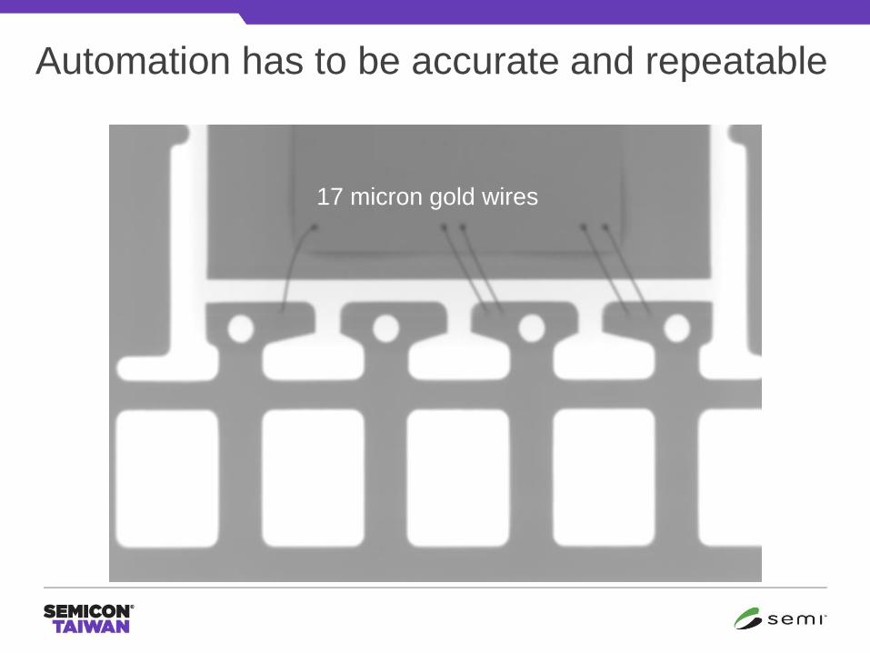
Automation has to be accurate and repeatable
17 micron gold wires
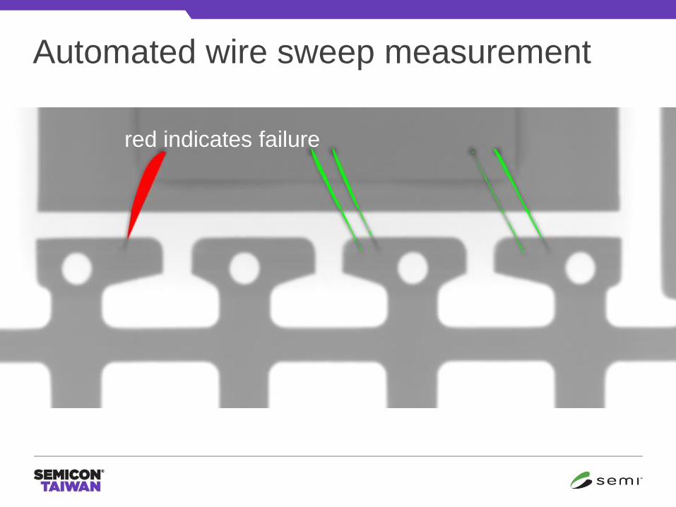
Automated wire sweep measurement
red indicates failure

Computed Tomography Advances
Advanced x-ray
systems provide fast
scanning
QuickScan delivers
almost as good result
but much faster, in 3 to
5 minutes versus more
than 30 minutes
Conventional µCT (left) and QuickScan
(right) of a BGA with volume views (top)
and views of a slice (bottom)

QuickScan Plus
QuickScan Plus - volume view and
virtual cross-sections of micro-BGA
with micro-vias, wedge bonding
HPR x-ray tube target
TXI (True Intensity
Control)
10-15W target power
Real Time Flat Panel
Detector
64bit CT High Speed
reconstruction
software

Cracked Passive caused by interfacial voiding

Challenges of MicroelectronicsAs component engineers escalate from 2D single die
designs to 3D multiple die package solutions, it sets high
demands for inspection tools.

Challenges of Microelectronics
Thinned die cracking
Stacked packages must be able
to maintain the Z-height of a
standard package, requiring
thinned die down to 50μm
Thinned dies make stacked
components susceptible to
brittle fracture failures
Die cracking is a significant
concern with stacked packages
Cracked die
Die cracking

Challenges of Microelectronics
Flip chip connections
In most current 3D packages,
the stacked chips are
connected along their edges
with wire bonds
Also flip chip bumps are used
to create an interconnection
between stacked dies
Potential defects of flip-chip
bumping – opens and solder
voidingFlip-chip pin grid array, FCPGA Flip
chip bump area voiding

Challenges of Microelectronics
Thru Silicon Via (TSV)
connections
TSV replaces edge wiring by
creating vertical connections
through the body of the chips
A TSV is a via hole in a silicon
wafer, which is insulated and
filled with a conductive fill,
usually copper
Micro void in 30μm diameter TSV

Head on Pillow, 30µm µBGA balls
chip structure easily visible

35µm µBGA ball with voiding and open circuit (HoP)

25µm diameter copper pillars 50µm long, 2D angled view

2D angled view of 20µm TSV µbumps

Voiding measurement of 15µm copper pillar

3D image of 6µm diameter TSV’s

25µm Copper Pillars and 6µm TSV µBump connections

Automated measurement of blind and buried µvias

Thanks for your AttentionAny Questions?