Embed Size (px)
Citation preview
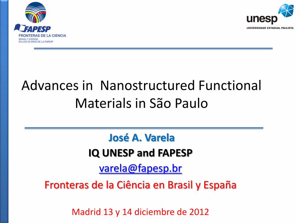
Advances in Nanostructured Functional Materials in São Paulo
José A. Varela
IQ UNESP and FAPESP
Fronteras de la Ciência en Brasil y España
Madrid 13 y 14 diciembre de 2012
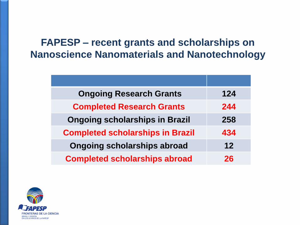
Ongoing Research Grants 124
Completed Research Grants 244
Ongoing scholarships in Brazil 258
Completed scholarships in Brazil 434
Ongoing scholarships abroad 12
Completed scholarships abroad 26
FAPESP – recent grants and scholarships on
Nanoscience Nanomaterials and Nanotechnology
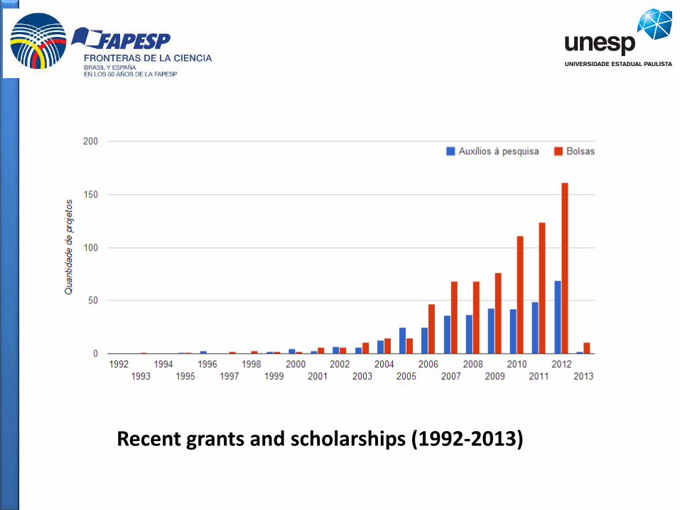
Recent grants and scholarships (1992-2013)
0
100
200
300
400
500
600
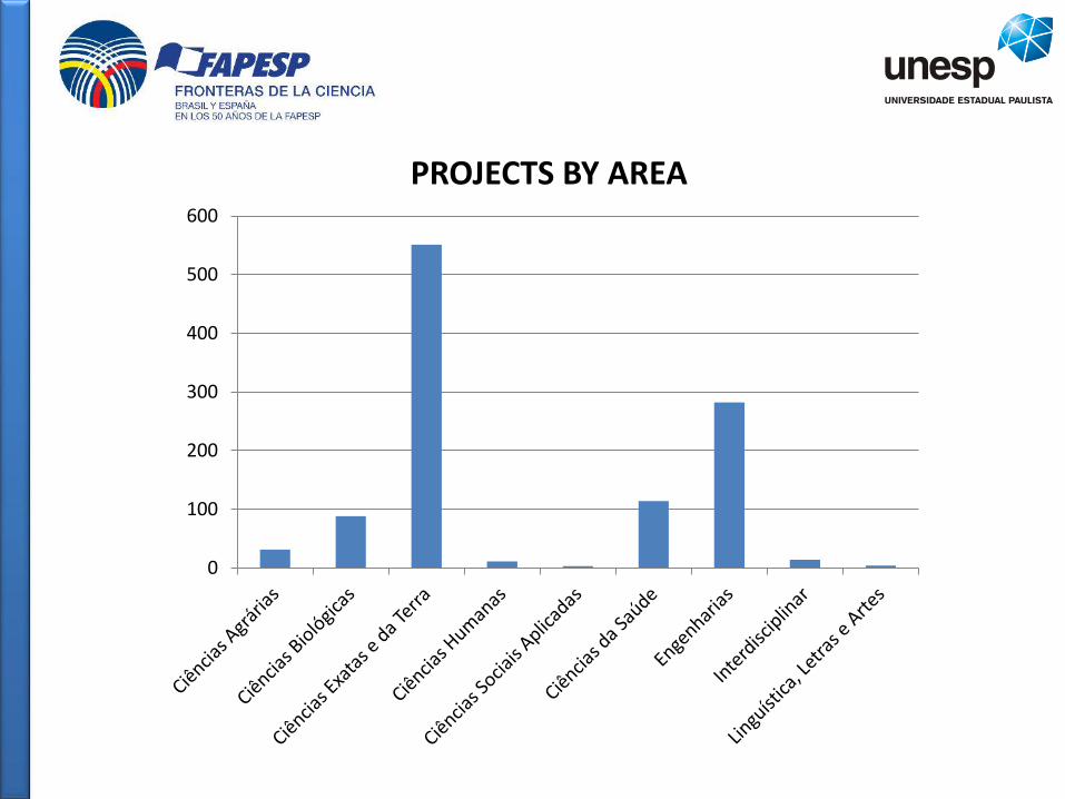
PROJECTS BY AREA
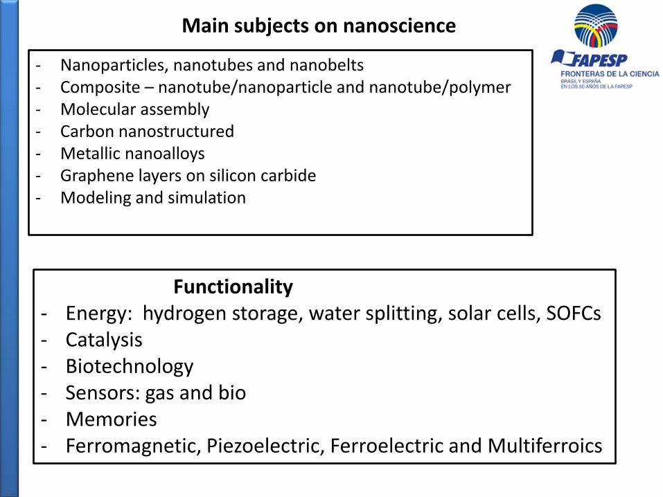
Main subjects on nanoscience
- Nanoparticles, nanotubes and nanobelts - Composite – nanotube/nanoparticle and nanotube/polymer - Molecular assembly - Carbon nanostructured - Metallic nanoalloys - Graphene layers on silicon carbide - Modeling and simulation
Functionality - Energy: hydrogen storage, water splitting, solar cells, SOFCs - Catalysis - Biotechnology - Sensors: gas and bio - Memories - Ferromagnetic, Piezoelectric, Ferroelectric and Multiferroics
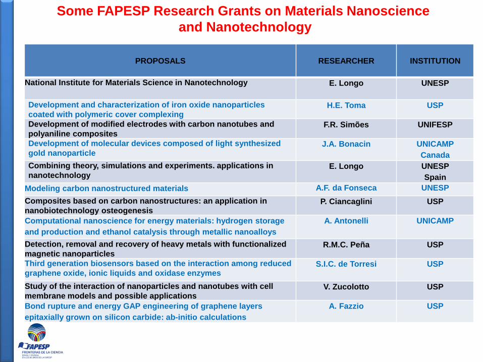
PROPOSALS
RESEARCHER
INSTITUTION
National Institute for Materials Science in Nanotechnology
E. Longo UNESP
Development and characterization of iron oxide nanoparticles
coated with polymeric cover complexing H.E. Toma USP
Development of modified electrodes with carbon nanotubes and
polyaniline composites F.R. Simões UNIFESP
Development of molecular devices composed of light synthesized
gold nanoparticle J.A. Bonacin UNICAMP
Canada
Combining theory, simulations and experiments. applications in
nanotechnology E. Longo UNESP
Spain
Modeling carbon nanostructured materials A.F. da Fonseca UNESP
Composites based on carbon nanostructures: an application in
nanobiotechnology osteogenesis P. Ciancaglini USP
Computational nanoscience for energy materials: hydrogen storage
and production and ethanol catalysis through metallic nanoalloys
A. Antonelli UNICAMP
Detection, removal and recovery of heavy metals with functionalized
magnetic nanoparticles R.M.C. Peña USP
Third generation biosensors based on the interaction among reduced
graphene oxide, ionic liquids and oxidase enzymes S.I.C. de Torresi USP
Study of the interaction of nanoparticles and nanotubes with cell
membrane models and possible applications V. Zucolotto USP
Bond rupture and energy GAP engineering of graphene layers
epitaxially grown on silicon carbide: ab-initio calculations
A. Fazzio USP
Some FAPESP Research Grants on Materials Nanoscience
and Nanotechnology
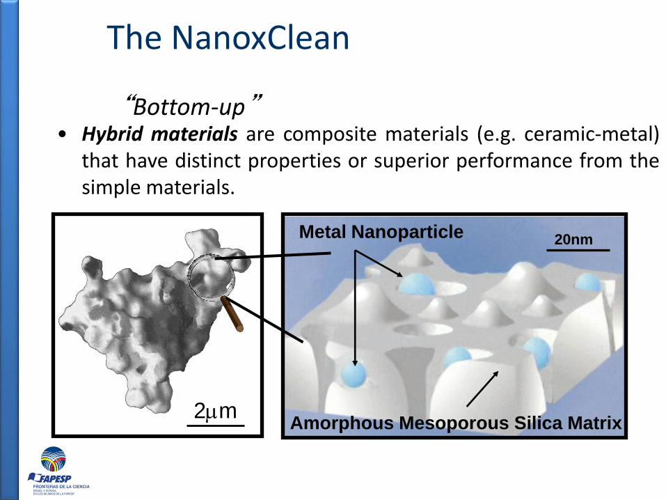
Metal Nanoparticle
Amorphous Mesoporous Silica Matrix
2m
20nm
“Bottom-up” • Hybrid materials are composite materials (e.g. ceramic-metal)
that have distinct properties or superior performance from the simple materials.
The NanoxClean
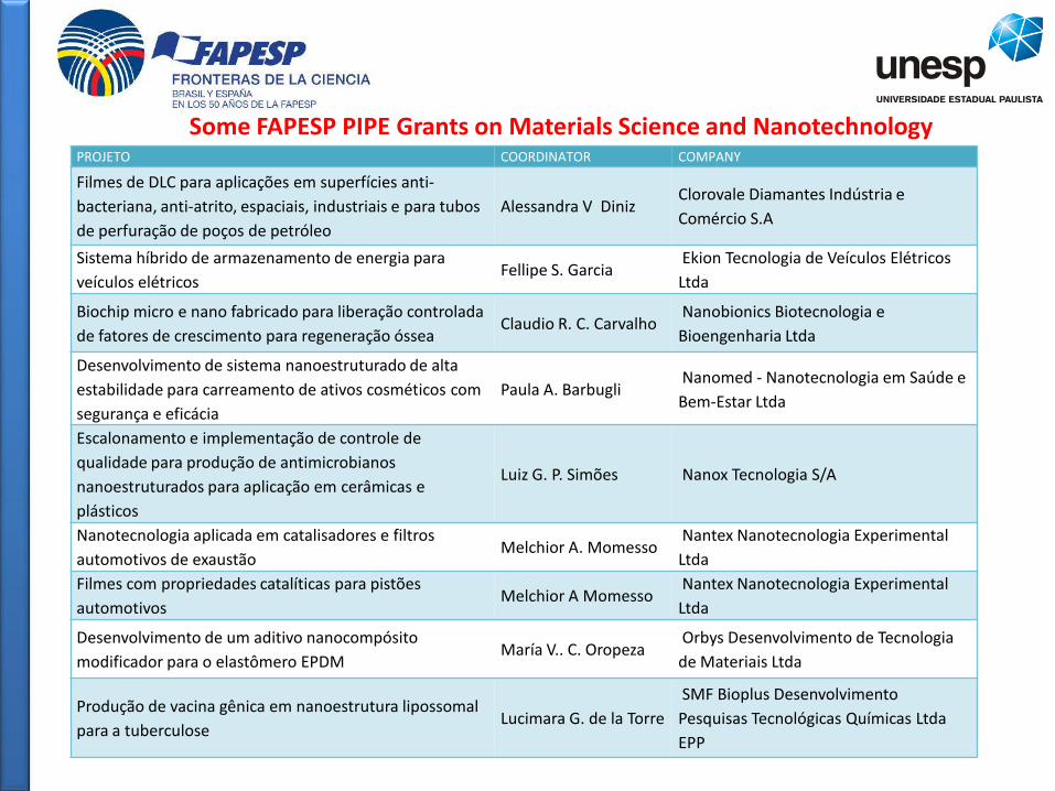
PROJETO COORDINATOR COMPANY
Filmes de DLC para aplicações em superfícies anti-
bacteriana, anti-atrito, espaciais, industriais e para tubos
de perfuração de poços de petróleo
Alessandra V Diniz Clorovale Diamantes Indústria e
Comércio S.A
Sistema híbrido de armazenamento de energia para
veículos elétricos Fellipe S. Garcia
Ekion Tecnologia de Veículos Elétricos
Ltda
Biochip micro e nano fabricado para liberação controlada
de fatores de crescimento para regeneração óssea Claudio R. C. Carvalho
Nanobionics Biotecnologia e
Bioengenharia Ltda
Desenvolvimento de sistema nanoestruturado de alta
estabilidade para carreamento de ativos cosméticos com
segurança e eficácia
Paula A. Barbugli Nanomed - Nanotecnologia em Saúde e
Bem-Estar Ltda
Escalonamento e implementação de controle de
qualidade para produção de antimicrobianos
nanoestruturados para aplicação em cerâmicas e
plásticos
Luiz G. P. Simões Nanox Tecnologia S/A
Nanotecnologia aplicada em catalisadores e filtros
automotivos de exaustão Melchior A. Momesso
Nantex Nanotecnologia Experimental
Ltda
Filmes com propriedades catalíticas para pistões
automotivos Melchior A Momesso
Nantex Nanotecnologia Experimental
Ltda
Desenvolvimento de um aditivo nanocompósito
modificador para o elastômero EPDM María V.. C. Oropeza
Orbys Desenvolvimento de Tecnologia
de Materiais Ltda
Produção de vacina gênica em nanoestrutura lipossomal
para a tuberculose Lucimara G. de la Torre
SMF Bioplus Desenvolvimento
Pesquisas Tecnológicas Químicas Ltda
EPP
Some FAPESP PIPE Grants on Materials Science and Nanotechnology
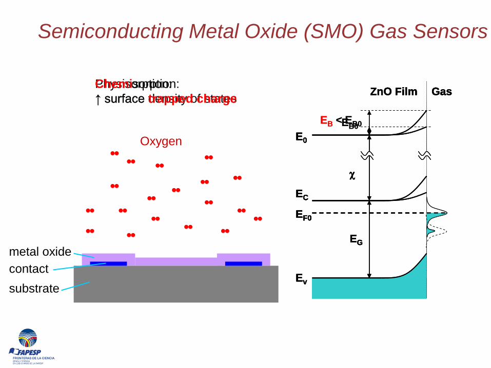
Ev
EC
EF0
EG
EB0
E0
ZnO Film Gas
Ev
EC
EF0
EG
EB0
E0
ZnO Film Gas
Ev
EC
EF0
EG
E0
ZnO Film Gas
EB < EB0
Ev
EC
EF0
EG
E0
ZnO Film Gas
EB < EB0
Semiconducting Metal Oxide (SMO) Gas Sensors
substrate
contact
metal oxide
Oxygen
Physisorption:
↑ surface density of states
Chemisorption:
↑ surface trapped charge
20 30 40 50 60 70
(210)
(202)
(301)
(112)
(310)
(002)
(220)
(211)
(200)
(111)
(101)
Inte
nsid
ad
e / u
.a.
2graus
a)
b)
(110)
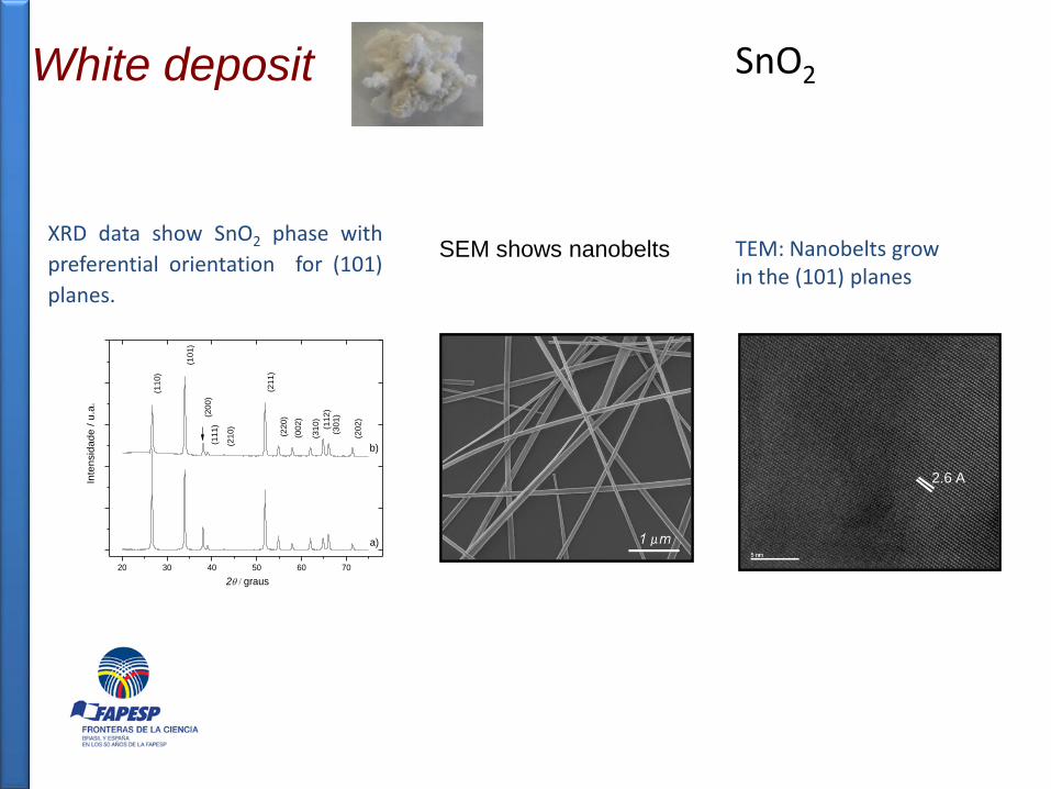
XRD data show SnO2 phase with
preferential orientation for (101)
planes.
White deposit
SEM shows nanobelts
2.6 A
TEM: Nanobelts grow in the (101) planes
SnO2
SEM: Nanobelts
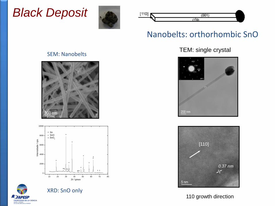
Black Deposit
TEM: single crystal
Nanobelts: orthorhombic SnO
[110]
110 growth direction
10 20 30 40 50 60 70 80
0
2000
4000
6000
8000
10000
+## +
* *##*%+
*
*
#
*
*
*
*
*
*
*
SnO2
Inte
nsid
ad
e / c
ps
2 / graus
#
+
SnO
Sn
XRD: SnO only
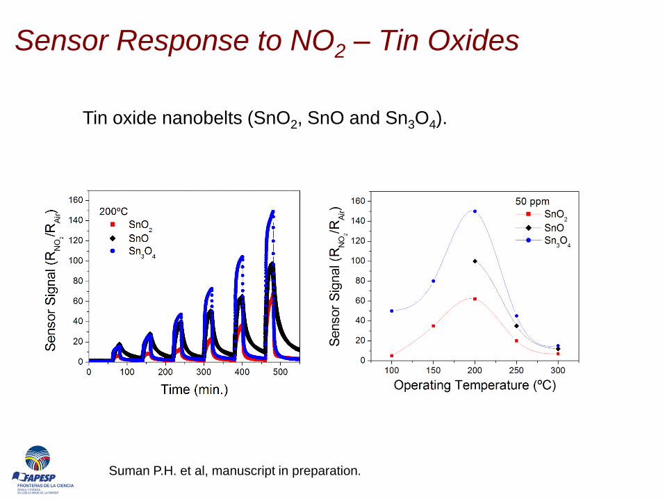
Sensor Response to NO2 – Tin Oxides
Tin oxide nanobelts (SnO2, SnO and Sn3O4).
Suman P.H. et al, manuscript in preparation.
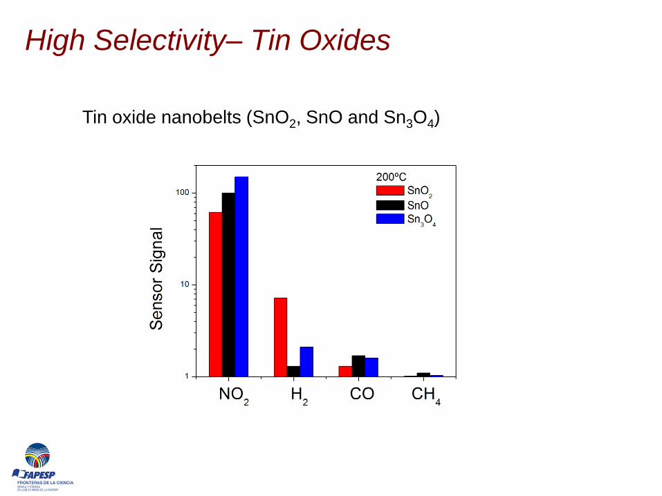
High Selectivity– Tin Oxides
Tin oxide nanobelts (SnO2, SnO and Sn3O4)
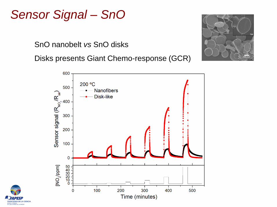
Sensor Signal – SnO
SnO nanobelt vs SnO disks
Disks presents Giant Chemo-response (GCR)
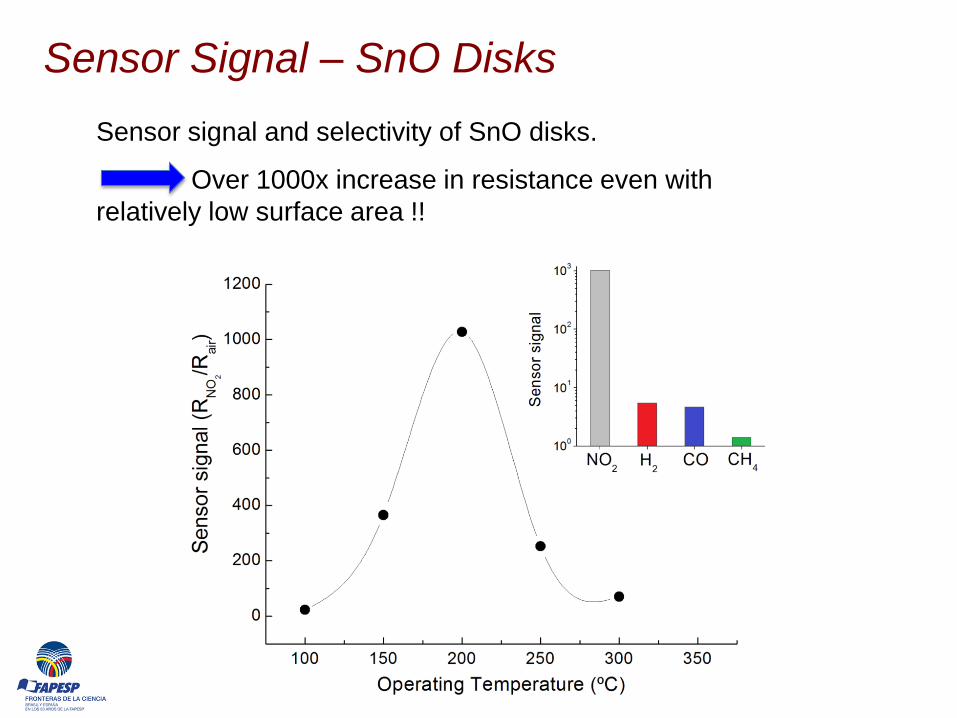
Sensor Signal – SnO Disks
Sensor signal and selectivity of SnO disks.
Over 1000x increase in resistance even with
relatively low surface area !!
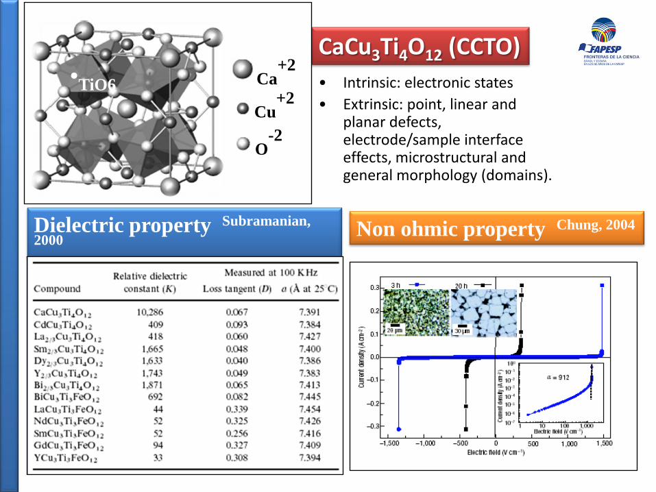
CaCu3Ti4O12 (CCTO)
Ca+2
Cu+2
O-2
•TiO6
Non ohmic property Chung, 2004 Dielectric property Subramanian,
2000
• Intrinsic: electronic states
• Extrinsic: point, linear and planar defects, electrode/sample interface effects, microstructural and general morphology (domains).
467 466 465 464 463 462 461 460 459 458 457 456 455
CCTO 72h
CCTO 20h
2p1/2
2p3/2
CCTO 3h
458
458.4
457.6
458.9
457.9
Inte
ns
ity
(a
.u.)
459.1
Ti 2p
Binding Energy (eV)
946 944 942 940 938 936 934 932 930 928
Binding Energy (eV)
Inte
ns
ity
(a
.u.)
933.2
934.8
934.5
933.3
CCTO 72h
CCTO 20h
CCTO 3h
2p1/2
2p3/2
931.5
931.6
935.2
933.4
931.7
Cu 2p
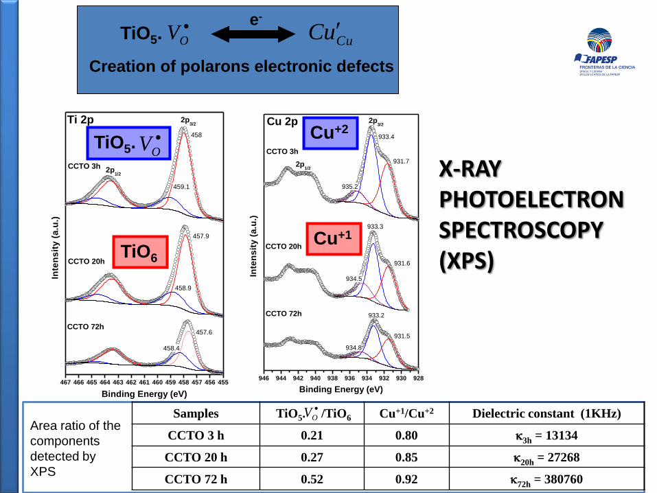
Samples TiO5. /TiO6 Cu+1/Cu+2 Dielectric constant (1KHz)
CCTO 3 h 0.21 0.80 k3h= 13134
CCTO 20 h 0.27 0.85 k20h = 27268
CCTO 72 h 0.52 0.92 k72h = 380760
OV
Cu+2
Cu+1
TiO5.
OV
TiO6
Area ratio of the
components
detected by
XPS
X-RAY PHOTOELECTRON SPECTROSCOPY (XPS)
TiO5.
OV CuuC e-
Creation of polarons electronic defects
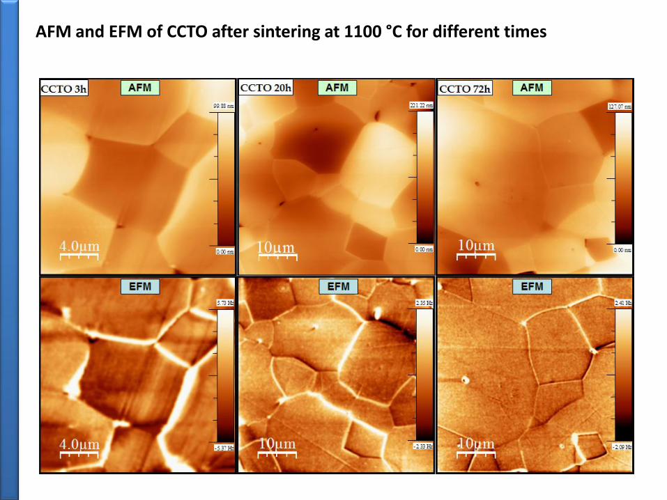
AFM and EFM of CCTO after sintering at 1100 °C for different times
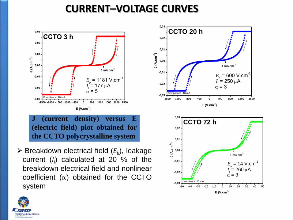
Breakdown electrical field (Eb), leakage
current (Il) calculated at 20 % of the
breakdown electrical field and nonlinear
coefficient () obtained for the CCTO
system
J (current density) versus E
(electric field) plot obtained for
the CCTO polycrystalline system
-50 -40 -30 -20 -10 0 10 20 30 40 50
-0,03
-0,02
-0,01
0,00
0,01
0,02
0,03
compliance: 10 mA
E (V.cm-1)
CCTO 72 h
= 3Il = 260 A
Eb = 14 V.cm
-1
J (
A.c
m-2
)
1 mA.cm-2
-2500 -2000 -1500 -1000 -500 0 500 1000 1500 2000 2500
-0,03
-0,02
-0,01
0,00
0,01
0,02
0,03
E (V.cm-1)
J (
A.c
m-2
)
= 5
Compliance: 10 mA
Eb = 1181 V.cm
-1
1 mA.cm-2
Il = 177 A
CCTO 3 h
-1600 -1200 -800 -400 0 400 800 1200 1600
-0,03
-0,02
-0,01
0,00
0,01
0,02
0,03
Compliance: 10 mA
CCTO 20 h
E (V.cm-1)
J (
A.c
m-2
)
= 3I
l = 250 A
Eb = 600 V.cm
-1
1 mA.cm-2
CURRENT–VOLTAGE CURVES
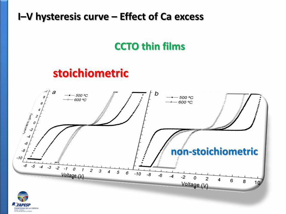
I–V hysteresis curve – Effect of Ca excess
stoichiometric
non-stoichiometric
CCTO thin films
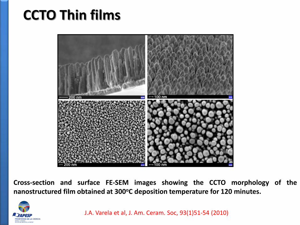
Cross-section and surface FE-SEM images showing the CCTO morphology of the nanostructured film obtained at 300oC deposition temperature for 120 minutes.
CCTO Thin films
J.A. Varela et al, J. Am. Ceram. Soc, 93(1)51-54 (2010)
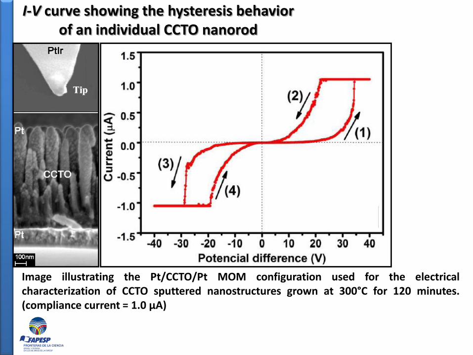
Image illustrating the Pt/CCTO/Pt MOM configuration used for the electrical characterization of CCTO sputtered nanostructures grown at 300°C for 120 minutes. (compliance current = 1.0 µA)
I-V curve showing the hysteresis behavior of an individual CCTO nanorod
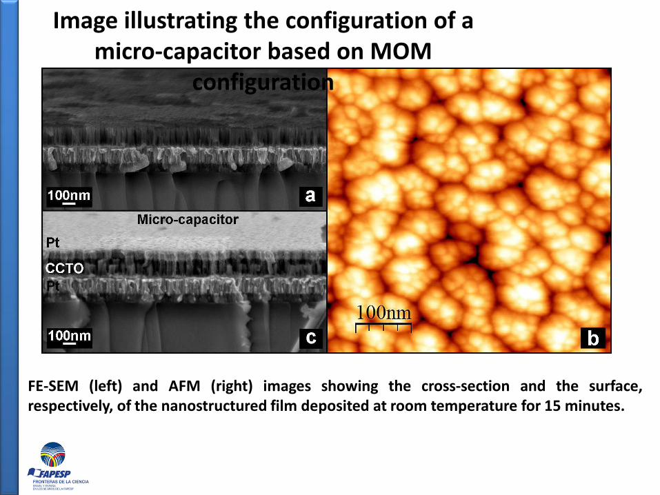
FE-SEM (left) and AFM (right) images showing the cross-section and the surface, respectively, of the nanostructured film deposited at room temperature for 15 minutes.
Image illustrating the configuration of a micro-capacitor based on MOM
configuration
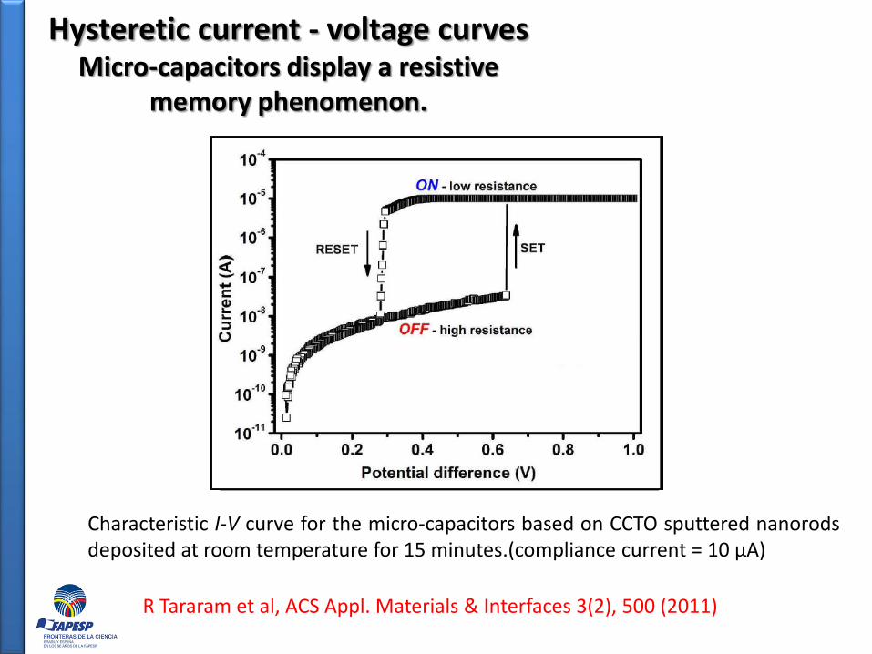
Characteristic I-V curve for the micro-capacitors based on CCTO sputtered nanorods deposited at room temperature for 15 minutes.(compliance current = 10 µA)
Hysteretic current - voltage curves Micro-capacitors display a resistive
memory phenomenon.
R Tararam et al, ACS Appl. Materials & Interfaces 3(2), 500 (2011)

Muchas Gracias