Embed Size (px)
Citation preview
Advances in DMD-Based UV Application Reliability Below 320nm
Jonathan T. Fong, Tom W. Winter, S. Josh Jacobs Texas Instruments Inc., 6550 Chase Oaks Blvd., Plano TX USA 75023
ABSTRACT
Texas Instrument’s spatial light modulator chip, the DMD (digital micromirror device, the central chip in all DLP® based systems) has been used in multiple maskless lithography applications for the past 5-7 years. Typically these applications have been focused on PCB lithography. Applications using illumination below 320nm have not been feasible due to shortened lifetime of the device at shorter wavelengths. Recent advances in DMD processing have made significant improvements in the operational lifetime of the DMD. This paper will cover the background of UV-A DMD maskless lithography and demonstrate the increased lifetime at 311nm and 266nm with the new processes.
Keywords: DMD, digital micromirror device, maskless lithography, PCB lithography, spatial UV modulation, deep UV reliability, DLP®, LCD repair
0. INTRODUCTION Multiple papers on maskless lithography using DMDs have been published by many universities, research centers and end equipment manufacturers. Production systems utilizing the DMD have been launched by multiple OEMs, including DNS, Fujifilm and Hitachi VIA. Typically these tools have been configured to use multiple mid to high resolution DMDs for high throughput and operate in the 365-410nm regime. Typical operating conditions are 3-5W/cm2 illumination on the DMD with temperature held below 30°C. Using these conditions, manufacturers have been able to match the throughput on the DMD systems with the mask-based systems.
Devices have consistently demonstrated operation in excess of 3000 hours at 3.4W/cm2, 25C in the UV-A range. The standard UV window used in production qualified UV DMDs has a usable transmission over 320-400nm. To test and operate the device at wavelengths lower than this, a special window is needed with high transmissivity below 320nm (quartz or sapphire). Latest performance data for both the current baseline process as well as the extended performance process will be presented.
1. DMD TECHNOLOGY OVERVIEW The DMD is a micro-opto-electro mechanical device (MOEM), an optical subset of the MEMS industry (micro-electro-mechanical systems). The device is an array of up to 2.8 million torsional hinge mounted micro-mirrors built on a standard CMOS memory cell for addressing each individual mirror. Mirrors can range from 7.5-14.8µm and are processed in a standard semiconductor plant, mostly using standard process equipment. Elecrostatics from the memory cell underneath the mirror actuate the rotation of the mirror on the torsional hinge to tilt it into either the “off” or “on” position, +/- 12 degrees from horizontal.
Alternative Lithographic Technologies II, edited by Daniel J. C. Herr, Proc. of SPIE Vol. 7637763718 · © 2010 SPIE · CCC code: 0277-786X/10/$18 · doi: 10.1117/12.848461
Proc. of SPIE Vol. 7637 763718-1
Downloaded From: http://spiedigitallibrary.org/ on 09/12/2012 Terms of Use: http://spiedl.org/terms
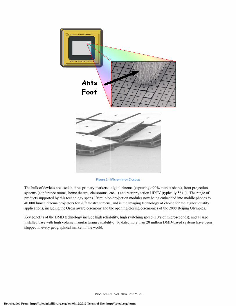
The bulk of dsystems (conproducts supp40,000 lumenapplications,
Key benefits installed baseshipped in ev
devices are usenference roomsported by this n cinema projeincluding the
of the DMD tee with high volvery geographi
ed in three prim, home theatretechnology spa
ectors for 70ft tOscar award c
echnology incllume manufactcal market in t
Figure 1 -
mary markets: , classrooms, eans 10cm3 picotheatre screenseremony and th
lude high reliabturing capabilitthe world.
Micromirror Clo
digital cinemaetc…) and rearo-projection mos, and is the imahe opening/clo
bility, high swity. To date, m
oseup
a (capturing >9r projection HDodules now beaging technolo
osing ceremoni
itching speed (more than 20 mi
0% market shaDTV (typically ing embedded
ogy of choice fies of the 2008
(10’s of microsillion DMD-ba
are), front proje58+”). The rainto mobile ph
for the highest q Beijing Olym
seconds), and aased systems ha
ection ange of hones to quality
mpics.
a large ave been
Proc. of SPIE Vol. 7637 763718-2
Downloaded From: http://spiedigitallibrary.org/ on 09/12/2012 Terms of Use: http://spiedl.org/terms
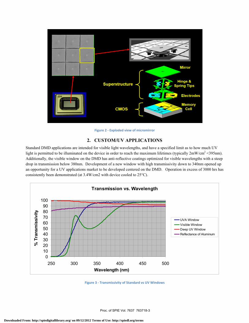
Figure 2 - Exploded view of micromirror
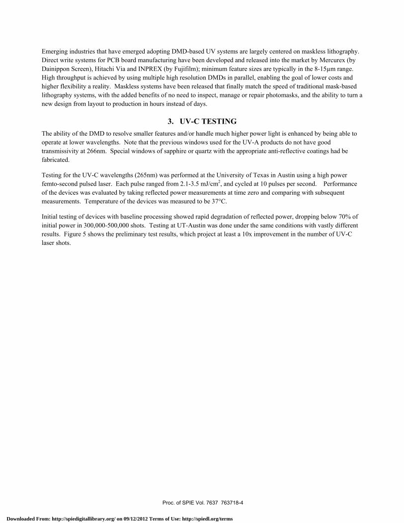
2. CUSTOM/UV APPLICATIONS Standard DMD applications are intended for visible light wavelengths, and have a specified limit as to how much UV light is permitted to be illuminated on the device in order to reach the maximum lifetimes (typically 2mW/cm2 <395nm). Additionally, the visible window on the DMD has anti-reflective coatings optimized for visible wavelengths with a steep drop in transmission below 380nm. Development of a new window with high transmissivity down to 340nm opened up an opportunity for a UV applications market to be developed centered on the DMD. Operation in excess of 3000 hrs has consistently been demonstrated (at 3.4W/cm2 with device cooled to 25°C).
Figure 3 - Transmissivity of Standard vs UV Windows
Transmission vs. Wavelength
0102030405060708090
100
250 300 350 400 450 500Wavelength (nm)
% T
rans
mis
sivi
ty
UVA WindowVisible WindowDeep UV WindowReflectance of Aluminum
Proc. of SPIE Vol. 7637 763718-3
Downloaded From: http://spiedigitallibrary.org/ on 09/12/2012 Terms of Use: http://spiedl.org/terms
Emerging industries that have emerged adopting DMD-based UV systems are largely centered on maskless lithography. Direct write systems for PCB board manufacturing have been developed and released into the market by Mercurex (by Dainippon Screen), Hitachi Via and INPREX (by Fujifilm); minimum feature sizes are typically in the 8-15µm range. High throughput is achieved by using multiple high resolution DMDs in parallel, enabling the goal of lower costs and higher flexibility a reality. Maskless systems have been released that finally match the speed of traditional mask-based lithography systems, with the added benefits of no need to inspect, manage or repair photomasks, and the ability to turn a new design from layout to production in hours instead of days.
3. UV-C TESTING The ability of the DMD to resolve smaller features and/or handle much higher power light is enhanced by being able to operate at lower wavelengths. Note that the previous windows used for the UV-A products do not have good transmissivity at 266nm. Special windows of sapphire or quartz with the appropriate anti-reflective coatings had be fabricated.
Testing for the UV-C wavelengths (265nm) was performed at the University of Texas in Austin using a high power femto-second pulsed laser. Each pulse ranged from 2.1-3.5 mJ/cm2, and cycled at 10 pulses per second. Performance of the devices was evaluated by taking reflected power measurements at time zero and comparing with subsequent measurements. Temperature of the devices was measured to be 37°C.
Initial testing of devices with baseline processing showed rapid degradation of reflected power, dropping below 70% of initial power in 300,000-500,000 shots. Testing at UT-Austin was done under the same conditions with vastly different results. Figure 5 shows the preliminary test results, which project at least a 10x improvement in the number of UV-C laser shots.
Proc. of SPIE Vol. 7637 763718-4
Downloaded From: http://spiedigitallibrary.org/ on 09/12/2012 Terms of Use: http://spiedl.org/terms
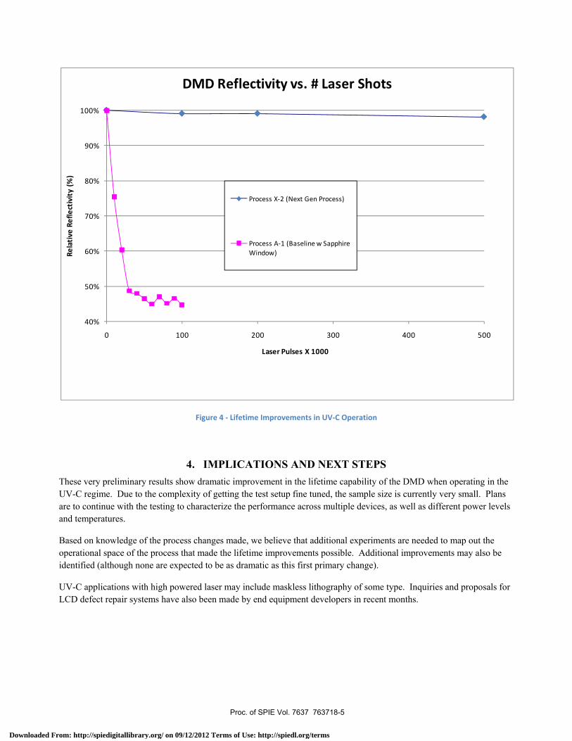
Figure 4 - Lifetime Improvements in UV-C Operation
4. IMPLICATIONS AND NEXT STEPS These very preliminary results show dramatic improvement in the lifetime capability of the DMD when operating in the UV-C regime. Due to the complexity of getting the test setup fine tuned, the sample size is currently very small. Plans are to continue with the testing to characterize the performance across multiple devices, as well as different power levels and temperatures.
Based on knowledge of the process changes made, we believe that additional experiments are needed to map out the operational space of the process that made the lifetime improvements possible. Additional improvements may also be identified (although none are expected to be as dramatic as this first primary change).
UV-C applications with high powered laser may include maskless lithography of some type. Inquiries and proposals for LCD defect repair systems have also been made by end equipment developers in recent months.
40%
50%
60%
70%
80%
90%
100%
0 100 200 300 400 500
Rela
tive
Ref
lect
ivit
y (%
)
Laser Pulses X 1000
DMD Reflectivity vs. # Laser Shots
Process X-2 (Next Gen Process)
Process A-1 (Baseline w Sapphire Window)
Proc. of SPIE Vol. 7637 763718-5
Downloaded From: http://spiedigitallibrary.org/ on 09/12/2012 Terms of Use: http://spiedl.org/terms
5. SUMMARY AND ACKNOWLEDGEMENTS The useful operation of the DMD in the UV-A wavelengths has been known and exploited for some years. UV-C operation at reasonable lifetimes has not been possible due to the rapid degradation of the device at 266nm. The latest process improvements have increased the lifetime of UV-C operation by an order of magnitude, based on early test results. We believe that this may put the DMD into the regime where the useful lifetime of the device is enough to make it a viable solution for various 266nm applications, which may include maskless lithography and LCD defect repair.
The authors wish to acknowledge the great work from the UT-Austin testing lab, done by Max Darnell and sponsored by lab director Prof. Shaochen Chen.
REFERENCES
1. “High-resolution maskless lithography”, Kin Foong Chan, et.al., Ball Semiconductor, JM3 October 2003/Vol 2(4) page 331
2. “Maskless, parallel patterning with zone-plate array lithography”, D.J.D. Carter, et.al., J. Vac. Sci. Technol. B 17(6), Nov/Dec 1999, page 3449
3. “Spatial Light Modulators for Maskless Lithography”, O. Solgaard, et.al., IEEE WA2 2006, page 150. 4. “Frequency analysis of maskless lithography”, Carsten Glasenapp, et.al., Optical Engineering, February
2008/Vol. 47(2), page 023002-1 5. “MOEMS-based lithography for the fabrication of micro-optical components”, Lars Erdmann, et.al. Carl Zeiss
Jenna GmbH, J. Microlith. Microfab., Microsyst. Oct-Dec 2005/Vol 4(4), page 041601
Proc. of SPIE Vol. 7637 763718-6
Downloaded From: http://spiedigitallibrary.org/ on 09/12/2012 Terms of Use: http://spiedl.org/terms