Embed Size (px)
Citation preview

Innovation, Science and Economic Development Canada
Innovation, Sciences et Développement économique Canada
Advanced Qualification Question Bank for Amateur Radio Operator Certificate
Examinations
Spectrum Management and Telecommunications 20 April, 2018
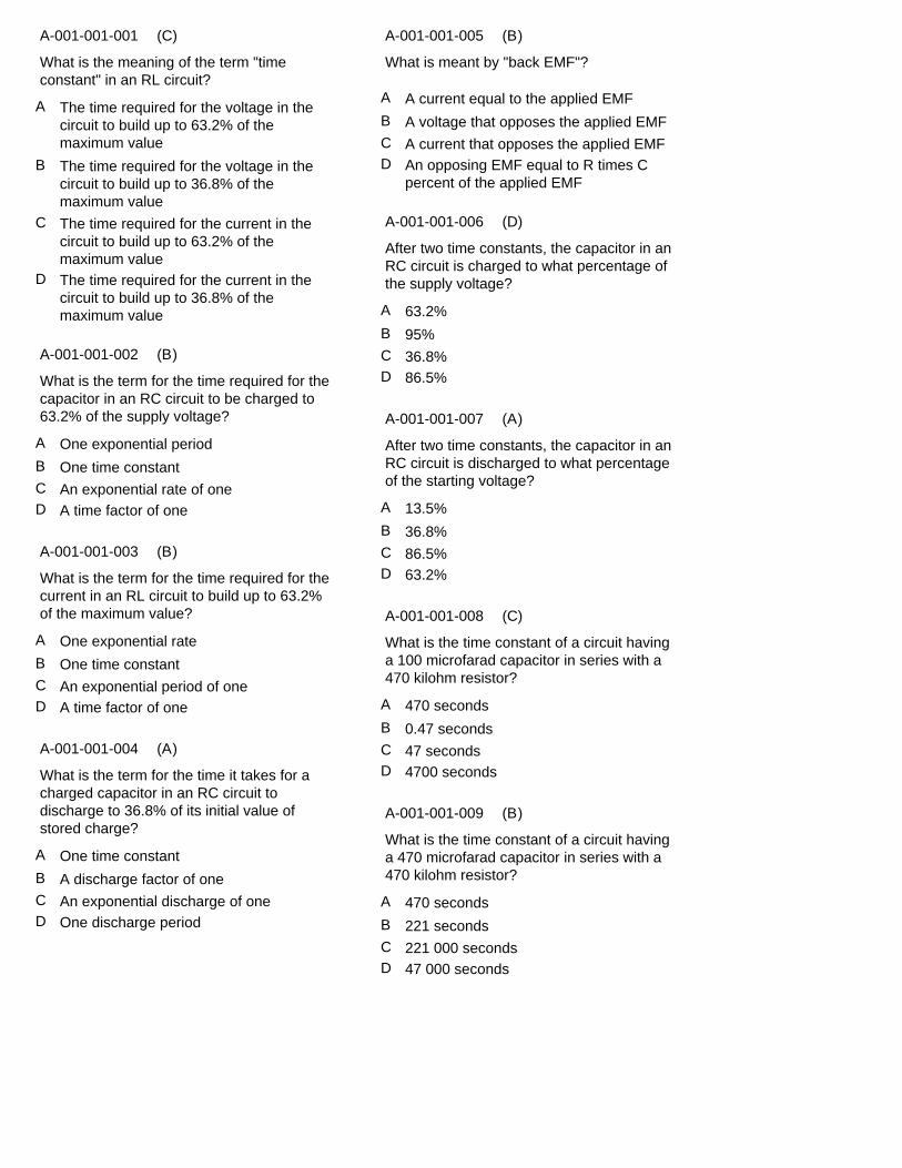
Foreword:This question bank contains the questions that will be used effective the date printed on the title page, for making Advanced Qualification examinations for the Amateur Radio Operator Certificate. The correct choice of the four suggested answers appears in brackets following each question identifier. i.e. A-001-001-001 (D)
While every reasonable effort has been made to ensure accuracy in this document, no warranty is expressed or implied. Candidates for amateur radio operator certificate examinations are encouraged to contact thefollowing amateur radio organizations for information on study material. Radio Amateurs of Canada720 Belfast Road, Suite 217Ottawa, OntarioK1G 0Z5www.rac.ca Radio Amateur du Québec inc.4545 Pierre-de-Coubertin AvenueC.P. 1000, Succursale MMontréal, QuebecH1V 3R2www.raqi.qc.ca Instructions for examiners are contained in Radiocommunication Information Circular RIC-1, Guide for Examiners Accredited to Conduct Examinations for the Amateur Radio Operator Certificate.
For additional information, please contact the Amateur Radio Service Centre:
Industry CanadaAmateur Radio Service Centre2 Queen Street EastSault Ste. Marie, ON P6A 1Y3
E-mail address: [email protected]: 1-888-780-3333 (Toll free)Fax number: 1-705-941-4607
A-001-001-001
A-001-001-002
A-001-001-003
A-001-001-004
A-001-001-005
A-001-001-006
A-001-001-007
A-001-001-008
A-001-001-009
The time required for the voltage in the circuit to build up to 63.2% of the maximum value
One exponential period
One exponential rate
One time constant
A current equal to the applied EMF
63.2%
13.5%
470 seconds
470 seconds
The time required for the voltage in the circuit to build up to 36.8% of the maximum value
One time constant
One time constant
A discharge factor of one
A voltage that opposes the applied EMF
95%
36.8%
0.47 seconds
221 seconds
The time required for the current in the circuit to build up to 63.2% of the maximum value
An exponential rate of one
An exponential period of one
An exponential discharge of one
A current that opposes the applied EMF
36.8%
86.5%
47 seconds
221 000 seconds
The time required for the current in the circuit to build up to 36.8% of the maximum value
A time factor of one
A time factor of one
One discharge period
An opposing EMF equal to R times C percent of the applied EMF
86.5%
63.2%
4700 seconds
47 000 seconds
What is the meaning of the term "time constant" in an RL circuit?
What is the term for the time required for thecapacitor in an RC circuit to be charged to 63.2% of the supply voltage?
What is the term for the time required for thecurrent in an RL circuit to build up to 63.2% of the maximum value?
What is the term for the time it takes for a charged capacitor in an RC circuit to discharge to 36.8% of its initial value of stored charge?
What is meant by "back EMF"?
After two time constants, the capacitor in anRC circuit is charged to what percentage of the supply voltage?
After two time constants, the capacitor in anRC circuit is discharged to what percentage of the starting voltage?
What is the time constant of a circuit having a 100 microfarad capacitor in series with a 470 kilohm resistor?
What is the time constant of a circuit having a 470 microfarad capacitor in series with a 470 kilohm resistor?
A
A
A
A
A
A
A
A
A
B
B
B
B
B
B
B
B
B
C
C
C
C
C
C
C
C
C
D
D
D
D
D
D
D
D
D
(C)
(B)
(B)
(A)
(B)
(D)
(A)
(C)
(B)

A-001-001-010
A-001-002-001
A-001-002-002
A-001-002-003
A-001-002-004
A-001-002-005
A-001-002-006
A-001-002-007
A-001-002-008
470 seconds
Thermal effects on the surface of the conductor decrease impedance
Layer effect
In the centre of the conductor
Because of skin effect
Because the insulation conducts current at high frequencies
Watt
a skin effect that diminishes with distance
In the same direction as the current
220 seconds
As frequency increases, RF current flowsin a thinner layer of the conductor, closer to the surface
Skin effect
Along the surface of the conductor
Because the RF resistance of a conductor is much less than the DC resistance
Because of skin effect
Volt
an electromagnetic field
In the direct opposite to the current
103 seconds
As frequency decreases, RF current flows in a thinner layer of the conductor, closer to the surface
Piezoelectric effect
In a magnetic field in the centre of the conductor
Because a conductor has AC resistance due to self-inductance
Because of the Hertzberg effect
Farad
an electrostatic field
In the direction determined by the left-hand rule
470 000 seconds
Thermal effects on the surface of the conductor increase impedance
Resonance effect
In a magnetic field around the conductor
Because of heating of the conductor's interior
Because conductors are non-linear devices
Coulomb
a cloud of electrons
In all directions
What is the time constant of a circuit having a 220 microfarad capacitor in series with a 470 kilohm resistor?
What is the result of skin effect?
What effect causes most of an RF current toflow along the surface of a conductor?
Where does almost all RF current flow in a conductor?
Why does most of an RF current flow within a very thin layer under the conductor's surface?
Why is the resistance of a conductor different for RF currents than for direct currents?
What unit measures the ability of a capacitor to store electrical charge?
A wire has a current passing through it. Surrounding this wire there is:
In what direction is the magnetic field oriented about a conductor in relation to the direction of electron flow?
A
A
A
A
A
A
A
A
A
B
B
B
B
B
B
B
B
B
C
C
C
C
C
C
C
C
C
D
D
D
D
D
D
D
D
D
(C)
(B)
(B)
(B)
(A)
(B)
(C)
(B)
(C)

A-001-002-009
A-001-002-010
A-001-002-011
A-001-003-001
A-001-003-002
A-001-003-003
A-001-003-004
A-001-003-005
A-001-003-006
A-001-003-007
Ampere-joules
a magnetic field
henry
7.96 MHz
1.99 MHz
7.12 kHz
63.7 MHz
13.1 MHz
19.9 MHz
28.4 MHz
Joule-coulombs
a cloud of electrons
coulomb
79.6 MHz
1.78 kHz
3.18 MHz
10.1 kHz
13.1 kHz
19.9 kHz
2.84 MHz
Potential energy
an electric current
farad
3.56 MHz
1.78 MHz
3.18 kHz
63.7 kHz
14.5 kHz
17.8 kHz
2.13 MHz
Kinetic energy
an electrostatic field
watt
1.78 MHz
1.99 kHz
7.12 MHz
10.1 MHz
14.5 MHz
17.8 MHz
21.3 MHz
What is the term for energy that is stored in an electromagnetic or electrostatic field?
Between the charged plates of a capacitor there is:
Energy is stored within an inductor that is carrying a current. The amount of energy depends on this current, but it also depends on a property of the inductor. This property has the following unit:
What is the resonant frequency of a series RLC circuit if R is 47 ohms, L is 50 microhenrys and C is 40 picofarads?
What is the resonant frequency of a series RLC circuit, if R is 47 ohms, L is 40 microhenrys and C is 200 picofarads?
What is the resonant frequency of a series RLC circuit, if R is 47 ohms, L is 50 microhenrys and C is 10 picofarads?
What is the resonant frequency of a series RLC circuit, if R is 47 ohms, L is 25 microhenrys and C is 10 picofarads?
What is the resonant frequency of a series RLC circuit, if R is 47 ohms, L is 3 microhenrys and C is 40 picofarads?
What is the resonant frequency of a series RLC circuit, if R is 47 ohms, L is 4 microhenrys and C is 20 picofarads?
What is the resonant frequency of a series RLC circuit, if R is 47 ohms, L is 8 microhenrys and C is 7 picofarads?
A
A
A
A
A
A
A
A
A
A
B
B
B
B
B
B
B
B
B
B
C
C
C
C
C
C
C
C
C
C
D
D
D
D
D
D
D
D
D
D
(C)
(D)
(A)
(C)
(C)
(D)
(D)
(D)
(D)
(D)

A-001-003-008
A-001-003-009
A-001-003-010
A-001-003-011
A-001-004-001
A-001-004-002
A-001-004-003
A-001-004-004
A-001-004-005
A-001-004-006
35.4 MHz
49.7 kHz
17.7 MHz
44 microfarads
15.9 MHz
5.31 MHz
23.7 kHz
20.5 kHz
2.12 kHz
14.5 MHz
35.4 kHz
28.1 kHz
1.77 MHz
2.2 picofarads
50.3 MHz
5.31 kHz
3.54 MHz
20.5 MHz
2.12 MHz
1.33 kHz
23.7 kHz
28.1 MHz
53.1 MHz
44 picofarads
15.9 kHz
29.1 MHz
3.54 kHz
2.65 MHz
18.4 kHz
1.33 MHz
23.7 MHz
49.7 MHz
5.31 MHz
2.2 microfarads
50.3 kHz
29.1 kHz
23.7 MHz
2.65 kHz
18.4 MHz
14.5 kHz
What is the resonant frequency of a series RLC circuit, if R is 47 ohms, L is 3 microhenrys and C is 15 picofarads?
What is the resonant frequency of a series RLC circuit, if R is 47 ohms, L is 4 microhenrys and C is 8 picofarads?
What is the resonant frequency of a series RLC circuit, if R is 47 ohms, L is 1 microhenry and C is 9 picofarads?
What is the value of capacitance (C) in a series R-L-C circuit, if the circuit resonant frequency is 14.25 MHz and L is 2.84 microhenrys?
What is the resonant frequency of a parallel RLC circuit if R is 4.7 kilohms, L is 1 microhenry and C is 10 picofarads?
What is the resonant frequency of a parallel RLC circuit if R is 4.7 kilohms, L is 2 microhenrys and C is 15 picofarads?
What is the resonant frequency of a parallel RLC circuit if R is 4.7 kilohms, L is 5 microhenrys and C is 9 picofarads?
What is the resonant frequency of a parallel RLC circuit if R is 4.7 kilohms, L is 2 microhenrys and C is 30 picofarads?
What is the resonant frequency of a parallel RLC circuit if R is 4.7 kilohms, L is 15 microhenrys and C is 5 picofarads?
What is the resonant frequency of a parallel RLC circuit if R is 4.7 kilohms, L is 3 microhenrys and C is 40 picofarads?
A
A
A
A
A
A
A
A
A
A
B
B
B
B
B
B
B
B
B
B
C
C
C
C
C
C
C
C
C
C
D
D
D
D
D
D
D
D
D
D
(D)
(C)
(C)
(C)
(B)
(C)
(D)
(B)
(D)
(A)

A-001-004-007
A-001-004-008
A-001-004-009
A-001-004-010
A-001-004-011
A-001-005-001
A-001-005-002
A-001-005-003
A-001-005-004
A-001-005-005
10.3 kHz
7.12 MHz
7.96 MHz
1.77 kHz
0.353 microhenry
7.51
0.023
0.00735
71.5
0.368
10.3 MHz
7.12 kHz
7.96 kHz
1.77 MHz
2.8 microhenrys
0.013
4.31
13.3
31.9
0.273
6.63 MHz
3.18 MHz
3.56 MHz
1.68 kHz
253.8 millihenrys
71.5
43.1
0.136
7.35
2.73
6.63 kHz
3.18 kHz
3.56 kHz
1.68 MHz
3.9 millihenrys
75.1
13.3
7.35
0.0319
36.8
What is the resonant frequency of a parallel RLC circuit if R is 4.7 kilohms, L is 40 microhenrys and C is 6 picofarads?
What is the resonant frequency of a parallel RLC circuit if R is 4.7 kilohms, L is 10 microhenrys and C is 50 picofarads?
What is the resonant frequency of a parallel RLC circuit if R is 4.7 kilohms, L is 200 microhenrys and C is 10 picofarads?
What is the resonant frequency of a parallel RLC circuit if R is 4.7 kilohms, L is 90 microhenrys and C is 100 picofarads?
What is the value of inductance (L) in a parallel RLC circuit, if the resonant frequency is 14.25 MHz and C is 44 picofarads?
What is the Q of a parallel RLC circuit, if it isresonant at 14.128 MHz, L is 2.7 microhenrys and R is 18 kilohms?
What is the Q of a parallel RLC circuit, if it isresonant at 14.128 MHz, L is 4.7 microhenrys and R is 18 kilohms?
What is the Q of a parallel RLC circuit, if it isresonant at 4.468 MHz, L is 47 microhenrys and R is 180 ohms?
What is the Q of a parallel RLC circuit, if it isresonant at 14.225 MHz, L is 3.5 microhenrys and R is 10 kilohms?
What is the Q of a parallel RLC circuit, if it isresonant at 7.125 MHz, L is 8.2 microhenrysand R is 1 kilohm?
A
A
A
A
A
A
A
A
A
A
B
B
B
B
B
B
B
B
B
B
C
C
C
C
C
C
C
C
C
C
D
D
D
D
D
D
D
D
D
D
(B)
(A)
(C)
(D)
(B)
(D)
(C)
(C)
(B)
(C)

A-001-005-006
A-001-005-007
A-001-005-008
A-001-005-009
A-001-005-010
A-001-005-011
A-002-001-001
A-002-001-002
A-002-001-003
A-002-001-004
0.00452
25.6
32.2
4.35
23
To decrease the Q and increase the bandwidth
Galena and germanium
In bipolar transistors
N-type
Superconductor
4.52
39
25.6
0.00435
1.84
To increase the Q and decrease the skin effect
Galena and bismuth
At microwave frequencies
Bipolar type
N-type
0.221
22.1
31.1
0.23
0.543
To decrease the Q and increase the resonant frequency
Silicon and gold
In high-power circuits
Superconductor type
P-type
22.1
0.0256
0.031
2.3
54.3
To increase the Q and decrease bandwidth
Silicon and germanium
At very low frequencies
P-type
Bipolar
What is the Q of a parallel RLC circuit, if it isresonant at 7.125 MHz, L is 10.1 microhenrys and R is 100 ohms?
What is the Q of a parallel RLC circuit, if it isresonant at 7.125 MHz, L is 12.6 microhenrys and R is 22 kilohms?
What is the Q of a parallel RLC circuit, if it isresonant at 3.625 MHz, L is 3 microhenrys and R is 2.2 kilohms?
What is the Q of a parallel RLC circuit, if it isresonant at 3.625 MHz, L is 42 microhenrys and R is 220 ohms?
What is the Q of a parallel RLC circuit, if it isresonant at 3.625 MHz, L is 43 microhenrys and R is 1.8 kilohms?
Why is a resistor often included in a parallel resonant circuit?
What two elements widely used in semiconductor devices exhibit both metallic and non-metallic characteristics?
In what application is gallium-arsenide used as a semiconductor material in preference togermanium or silicon?
What type of semiconductor material contains fewer free electrons than pure germanium or silicon crystals?
What type of semiconductor material contains more free electrons than pure germanium or silicon crystals?
A
A
A
A
A
A
A
A
A
A
B
B
B
B
B
B
B
B
B
B
C
C
C
C
C
C
C
C
C
C
D
D
D
D
D
D
D
D
D
D
(C)
(B)
(A)
(C)
(B)
(A)
(D)
(B)
(D)
(B)

A-002-001-005
A-002-001-006
A-002-001-007
A-002-001-008
A-002-001-009
A-002-001-010
A-002-001-011
A-002-002-001
A-002-002-002
A-002-002-003
A-002-002-004
Free neutrons
Holes
an insulator
intrinsic conductor
Tantalum
tuned circuits
impurities
A negative resistance region
Hot-carrier (Schottky)
As VHF and UHF mixers and detectors
Back EMF
Holes
Free protons
a superconductor
N-type conductor
Copper
inductors
protons
An internal capacitance that varies with the applied voltage
Varactor
As balanced mixers in FM generation
Peak inverse voltage
Free electrons
Free neutrons
a semiconductor
P-type conductor
Sulphur
insulators
ions
A constant voltage under conditions of varying current
Zener
As a variable capacitance in an automatic frequency control (AFC) circuit
Junction temperature
Free protons
Free electrons
a conductor
semiconductor
Silicon
conductors
electrons
A constant current under conditions of varying voltage
Silicon-controlled rectifier
As a constant voltage reference in a power supply
Forward voltage
What are the majority charge carriers in P-type semiconductor material?
What are the majority charge carriers in N-type semiconductor material?
Silicon, in its pure form, is:
An element which is sometimes an insulatorand sometimes a conductor is called a:
Which of the following materials is used to make a semiconductor?
Substances such as silicon in a pure state are usually good:
A semiconductor is said to be doped when ithas added to it small quantities of:
What is the principal characteristic of a Zener diode?
What type of semiconductor diode varies its internal capacitance as the voltage applied to its terminals varies?
What is a common use for the hot-carrier (Schottky) diode?
What limits the maximum forward current in a junction diode?
A
A
A
A
A
A
A
A
A
A
A
B
B
B
B
B
B
B
B
B
B
B
C
C
C
C
C
C
C
C
C
C
C
D
D
D
D
D
D
D
D
D
D
D
(B)
(D)
(A)
(D)
(D)
(C)
(A)
(C)
(B)
(A)
(C)

A-002-002-005
A-002-002-006
A-002-002-007
A-002-002-008
A-002-002-009
A-002-002-010
A-002-002-011
A-002-003-001
A-002-003-002
A-002-003-003
Maximum forward current and capacitance
Electrolytic and junction
As a constant voltage source
As a high voltage rectifier
decrease current
0.05
slightly greater
The change of collector current with respect to base current
The change of collector current with respect to emitter current
A varactor
Maximum reverse current and peak inverse voltage (PIV)
Junction and point contact
As a high voltage rectifier
As a constant voltage source
increase current
0.5
less
The change of base current with respect to collector current
The change of base current with respect to gate current
A triode vacuum tube
Maximum forward current and peak inverse voltage (PIV)
Vacuum and point contact
As an RF detector
As an RF switch
regulate voltage
5
the same
The change of collector current with respect to gate current
The change of collector current with respect to base current
A PNP transistor
Maximum reverse current and capacitance
Electrolytic and point contact
As a constant current source
As a constant current source
dissipate voltage
50
much greater
The change of collector current with respect to emitter current
The change of base current with respect to emitter current
An NPN transistor
What are the major ratings for junction diodes?
Structurally, what are the two main categories of semiconductor diodes?
What is a common use for point contact diodes?
What is one common use for PIN diodes?
A Zener diode is a device used to:
If a Zener diode rated at 10 V and 50 watts was operated at maximum dissipation rating, it would conduct ____ amperes:
The power-handling capability of most Zener diodes is rated at 25 degrees C or approximately room temperature. If the temperature is increased, the power handling capability is:
What is the alpha of a bipolar transistor?
What is the beta of a bipolar transistor?
Which component conducts electricity from a negative emitter to a positive collector when its base voltage is made positive?
A
A
A
A
A
A
A
A
A
A
B
B
B
B
B
B
B
B
B
B
C
C
C
C
C
C
C
C
C
C
D
D
D
D
D
D
D
D
D
D
(C)
(B)
(C)
(C)
(C)
(C)
(B)
(D)
(C)
(D)
A-002-003-004
A-002-003-005
A-002-003-006
A-002-003-007
A-002-003-008
A-002-003-009
A-002-003-010
A-002-003-011
A-002-004-001
A-002-004-002
Reverse voltage gain
beta
Common emitter
Common emitter or common gate
A PNP transistor
beta x (1 + beta)
usually about half
alpha x (1 - alpha)
An FET with a channel that blocks voltage through the gate
An FET without a channel to hinder current through the gate
Forward current gain
gamma
Common base
Common base or common collector
A triode vacuum tube
beta x (1 - beta)
high to very high
alpha x (1 + alpha)
An FET with a channel that allows current when the gate voltage is zero
An FET that has a channel that blocks current when the gate voltage is zero
Forward voltage gain
delta
Common collector
Common base or common emitter
A varactor
beta / (1 - beta)
very low
alpha / (1 - alpha)
An FET without a channel to hinder current through the gate
An FET that has a channel with no gate voltage applied; a current flows with zero gate voltage
Reverse current gain
alpha
Common gate
Common emitter or common collector
An NPN transistor
beta / (1 + beta)
usually about double
alpha / (1 + alpha)
An FET without a channel; no current occurs with zero gate voltage
An FET without a channel; no current flows with zero gate voltage
What is the alpha of a bipolar transistor in common base configuration?
In a bipolar transistor, the change of collector current with respect to base currentis called:
The alpha of a bipolar transistor is specified for what configuration?
The beta of a bipolar transistor is specified for what configurations?
Which component conducts electricity from a positive emitter to a negative collector when its base is made negative?
Alpha of a bipolar transistor is equal to:
The current gain of a bipolar transistor in common emitter or common collector compared to common base configuration is:
Beta of a bipolar transistor is equal to:
What is an enhancement-mode FET?
What is a depletion-mode FET?
A
A
A
A
A
A
A
A
A
A
B
B
B
B
B
B
B
B
B
B
C
C
C
C
C
C
C
C
C
C
D
D
D
D
D
D
D
D
D
D
(B)
(A)
(B)
(D)
(A)
(D)
(B)
(C)
(D)
(C)

A-002-004-003
A-002-004-004
A-002-004-005
A-002-004-006
A-002-004-007
A-002-004-008
A-002-004-009
A-002-004-010
A-002-004-011
A-002-005-001
The gate-protective Zener diode prevents the gate insulation from being punctured by small static charges or excessive voltages
They have micro-welded semiconductor junctions that are susceptible to breakage
The input impedance of FETs and bipolar transistors is the same
Emitter, base, collector
N-channel and P-channel
p-channel depletion
q-channel depletion
q-channel depletion
p-channel enhancement
Anode, cathode and gate
The gate-protective Zener diode keeps the gate voltage within specifications to prevent the device from overheating
They have fragile leads that may break off
An FET has high input impedance; a bipolar transistor has low input impedance
Gate 1, gate 2, drain
High power and low power
p-channel enhancement
p-channel enhancement
n-channel depletion
n-channel depletion
Gate, base 1 and base 2
The gate-protective Zener diode protects the substrate from excessive voltages
They are susceptible to damage from static charges
One cannot compare input impedance without knowing supply voltage
Gate, drain, source
MOSFET and GaAsFET
q-channel enhancement
p-channel depletion
p-channel depletion
n-channel enhancement
Base, collector and emitter
The gate-protective Zener diode provides a voltage reference to provide the correct amount of reverse-bias gate voltage
They are light-sensitive
An FET has low input impedance; a bipolar transistor has high input impedance
Emitter, base 1, base 2
Silicon and germanium
n-channel depletion
n-channel enhancement
n-channel enhancement
q-channel depletion
Gate, source and sink
Why do many MOSFET devices have built-ingate protective Zener diodes?
Why are special precautions necessary in handling FET and CMOS devices?
How does the input impedance of a field-effect transistor (FET) compare with that of abipolar transistor?
What are the three terminals of a junction field-effect transistor (JFET)?
What are the two basic types of junction field-effect transistors (JFET)?
Electron conduction in an n-channel depletion type MOSFET is associated with:
Electron conduction in an n-channel enhancement MOSFET is associated with:
Hole conduction in a p-channel depletion type MOSFET is associated with:
Hole conduction in a p-channel enhancement type MOSFET is associated with:
What are the three terminals of a silicon controlled rectifier (SCR)?
A
A
A
A
A
A
A
A
A
A
B
B
B
B
B
B
B
B
B
B
C
C
C
C
C
C
C
C
C
C
D
D
D
D
D
D
D
D
D
D
(A)
(C)
(B)
(C)
(A)
(D)
(D)
(C)
(A)
(A)

A-002-005-002
A-002-005-003
A-002-005-004
A-002-005-005
A-002-005-006
A-002-005-007
A-002-005-008
A-002-005-009
A-002-005-010
A-002-005-011
NPN conduction and PNP conduction
The varactor diode
When it is gated "off"
PPNN
gate
Varactors
Power supply overvoltage "crowbar" circuit
The field effect transistor
reverse-biased silicon rectifier
Hot carrier (Schottky) diode
Oscillating and quiescent
The junction diode
When it is used as a detector
PNPN
anode
Varistors
Class C amplifier circuit
The triode vacuum tube
forward-biased PIN diode
Zener diode
Conducting and non-conducting
The PIN diode
During a switching transition
NPPN
cathode
Thyristors
Microphone preamplifier circuit
The silicon controlled rectifier (SCR)
reverse-biased hot-carrier (Schottky) diode
Silicon controlled rectifier (SCR)
Forward conducting and reverse conducting
The hot-carrier (Schottky) diode
When it is gated "on"
PNNP
emitter
Phase locked loops
SWR detector circuit
The bipolar transistor
forward-biased silicon rectifier
PIN diode
What are the two stable operating conditionsof a silicon controlled rectifier (SCR)?
When a silicon controlled rectifier (SCR) is triggered, to what other semiconductor diodeare its electrical characteristics similar (as measured between its cathode and anode)?
Under what operating condition does a silicon controlled rectifier (SCR) exhibit electrical characteristics similar to a forward-biased silicon rectifier?
The silicon controlled rectifier (SCR) is what type of device?
The control element in the silicon controlled rectifier (SCR) is called the:
The silicon controlled rectifier (SCR) is a member of which family?
In amateur radio equipment, which is the major application for the silicon controlled rectifier (SCR)?
Which of the following devices has anode, cathode, and gate?
When it is gated "on", the silicon controlled rectifier (SCR) exhibits electrical characteristics similar to a:
Which of the following is a PNPN device?
A
A
A
A
A
A
A
A
A
A
B
B
B
B
B
B
B
B
B
B
C
C
C
C
C
C
C
C
C
C
D
D
D
D
D
D
D
D
D
D
(C)
(B)
(D)
(B)
(A)
(C)
(A)
(C)
(D)
(C)

A-002-006-001
A-002-006-002
A-002-006-003
A-002-006-004
A-002-006-005
A-002-006-006
A-002-006-007
A-002-006-008
A-002-006-009
A-002-006-010
Exactly 180 degrees
Class AB
Less than 180 degrees
Less than 180 degrees
Less than 180 degrees
Class AB
Class A
Class C
Class B
Class A
More than 180 degrees but less than 360degrees
Class B
More than 180 degrees but less than 360degrees
More than 180 degrees but less than 360degrees
More than 180 degrees but less than 360degrees
Class B
Class C
Class B
Class C
Class AB
Less than 180 degrees
Class C
Exactly 180 degrees
The entire cycle
The entire cycle
Class C
Class AB
Class AB
Class AB
Class B
The entire cycle
Class A
The entire cycle
180 degrees
180 degrees
Class A
Class B
Class A
Class A
Class C
For what portion of a signal cycle does a Class A amplifier operate?
Which class of amplifier has the highest linearity and least distortion?
For what portion of a cycle does a Class ABamplifier operate?
For what portion of a cycle does a Class B amplifier operate?
For what portion of a signal cycle does a Class C amplifier operate?
Which of the following classes of amplifier provides the highest efficiency?
Which of the following classes of amplifier would provide the highest efficiency in the output stage of a CW, RTTY or FM transmitter?
Which class of amplifier provides the least efficiency?
Which class of amplifier has the poorest linearity and the most distortion?
Which class of amplifier operates over the full cycle?
A
A
A
A
A
A
A
A
A
A
B
B
B
B
B
B
B
B
B
B
C
C
C
C
C
C
C
C
C
C
D
D
D
D
D
D
D
D
D
D
(D)
(D)
(B)
(D)
(A)
(C)
(B)
(D)
(B)
(A)
A-002-006-011
A-002-007-001
A-002-007-002
A-002-007-003
A-002-007-004
A-002-007-005
A-002-007-006
A-002-007-007
A-002-007-008
Class B
The input impedance is essentially determined by the resistance between the source and the drain
The output impedance is essentially determined by the drain supply voltage
Mutual gain, high stability and low mutualinductance
the output signals leads the input signal by 90 degrees
only slightly higher
the signals are 180 degrees out of phase
the signals are in phase
common drain circuit
Class C
The input impedance is essentially determined by the resistance between the drain and substrate
The output impedance is essentially determined by the gate supply voltage
Mutual gain, low input impedance and low output impedance
the signals are 180 degrees out of phase
only slightly lower
the output signal leads the input signal by 90 degrees
the output signal leads the input signal by 90 degrees
common source circuit
Class AB
The input impedance is essentially determined by the gate biasing network
The output impedance is essentially determined by the input impedance of theFET
Low output impedance, high mutual impedance and low output current
the signals are in phase
very high
the output signal lags the input signal by 90 degrees
the output signal lags the input signal by 90 degrees
common mode circuit
Class A
The input impedance is essentially determined by the resistance between the source and substrate
The output impedance is essentially determined by the drain resistor
High gain, high input impedance and low output impedance
the output signal lags the input signal by 90 degrees
very low
the signals are in phase
the signals are 180 degrees out of phase
common gate circuit
Which class of amplifier operates over less than 180 degrees of the cycle?
What determines the input impedance of a FET common-source amplifier?
What determines the output impedance of a FET common-source amplifier?
What are the advantages of a Darlington pairaudio amplifier?
In the common base amplifier, when the input and output signals are compared:
In the common base amplifier, the input impedance, when compared to the output impedance is:
In the common emitter amplifier, when the input and output signals are compared:
In the common collector amplifier, when the input and output signals are compared:
The FET amplifier source follower circuit is another name for:
A
A
A
A
A
A
A
A
A
B
B
B
B
B
B
B
B
B
C
C
C
C
C
C
C
C
C
D
D
D
D
D
D
D
D
D
(B)
(C)
(D)
(D)
(C)
(D)
(A)
(A)
(A)

A-002-007-009
A-002-007-010
A-002-007-011
A-002-008-001
A-002-008-002
A-002-008-003
A-002-008-004
A-002-008-005
Common collector
Common emitter
Common mode
An amplifier used to increase the averageoutput of frequency modulated amateur signals to the legal limit
Infinite input impedance, infinite output impedance, infinite gain and flat frequency response
The collector-to-base capacitance of the PNP stage
The potential between the amplifier input terminals of the op-amp in an open-loop condition
Exactly 1000 ohms
Common base
Common base
Common collector
A program subroutine that calculates the gain of an RF amplifier
Zero input impedance, infinite output impedance, infinite gain, and flat frequency response
The external feedback network
The output voltage of the op-amp minus its input voltage
Very high
Common mode
Common mode
Common emitter
A high-gain, direct-coupled differential amplifier whose characteristics are determined by components mounted externally
Infinite input impedance, zero output impedance, infinite gain, and flat frequency response
The PNP collector load
The potential between the amplifier input terminals of the op-amp in a closed-loop condition
Very low
Common emitter
Common collector
Common base
A high-gain, direct-coupled audio amplifier whose characteristics are determined by internal components of thedevice
Zero input impedance, zero output impedance, infinite gain, and flat frequency response
The voltage applied to the circuit
The difference between the output voltageof the op-amp and the input voltage required for the next stage
Exactly 100 ohms
The FET amplifier common source circuit is similar to which of the following bipolar transistor amplifier circuits?
The FET amplifier common drain circuit is similar to which of the following bipolar transistor amplifier circuits?
The FET amplifier common gate circuit is similar to which of the following bipolar transistor amplifier circuits?
What is an operational amplifier (op-amp)?
What would be the characteristics of the ideal op-amp?
What determines the gain of a closed-loop op-amp circuit?
What is meant by the term op-amp offset voltage?
What is the input impedance of a theoretically ideal op-amp?
A
A
A
A
A
A
A
A
B
B
B
B
B
B
B
B
C
C
C
C
C
C
C
C
D
D
D
D
D
D
D
D
(D)
(D)
(D)
(C)
(C)
(B)
(C)
(B)

A-002-008-006
A-002-008-007
A-002-008-008
A-002-008-009
A-002-008-010
A-002-008-011
A-002-009-001
A-002-009-002
Exactly 1000 ohms
Op-amps are fixed at one frequency
Op-amp circuits are used as audio filters for receivers
An operational amplifier circuit connectedsuch that the input and output signals are90 degrees out of phase
An operational amplifier circuit connectedsuch that the input and output signals are180 degrees out of phase
Difference amplifier
The elimination of noise in a wideband receiver by phase comparison
The original frequencies and the sum anddifference frequencies
Very low
Op-amps exhibit gain rather than insertion loss
Op-amp circuits are used as low-pass filters at the output of transmitters
An operational amplifier circuit connectedsuch that the input impedance is held to zero, while the output impedance is high
An operational amplifier circuit connectedsuch that the input and output signals arein phase
High gain audio amplifier
The combination of two signals to produce sum and difference frequencies
1.414 and 0.707 times the input frequencies
Very high
Op-amps are more rugged and can withstand more abuse than can LC elements
Op-amp circuits are used as filters for smoothing power supply output
An operational amplifier circuit connectedsuch that the input and output signals are180 degrees out of phase
An operational amplifier circuit connectedsuch that the input and output signals are90 degrees out of phase
Summing amplifier
The elimination of noise in a wideband receiver by phase differentiation
The sum, difference and square root of the input frequencies
Exactly 100 ohms
Op-amps are available in more styles andtypes than are LC elements
Op-amp circuits are used as high-pass filters to block RFI at the input of receivers
An operational amplifier circuit connectedsuch that the input and output signals arein phase
An operational amplifier circuit connectedsuch that the input impedance is held low, and the output impedance is high
Operational amplifier
The recovery of intelligence from a modulated signal
Two and four times the original frequency
What is the output impedance of a theoretically ideal op-amp?
What are the advantages of using an op-ampinstead of LC elements in an audio filter?
What are the principal uses of an op-amp RC active filter in amateur circuitry?
What is an inverting op-amp circuit?
What is a non-inverting op-amp circuit?
What term is most appropriate for a high gain, direct-coupled differential amplifier whose characteristics are determined by components mounted externally?
What is the mixing process?
What are the principal frequencies that appear at the output of a mixer circuit?
A
A
A
A
A
A
A
A
B
B
B
B
B
B
B
B
C
C
C
C
C
C
C
C
D
D
D
D
D
D
D
D
(B)
(B)
(A)
(C)
(B)
(D)
(B)
(A)

A-002-009-003
A-002-009-004
A-002-009-005
A-002-009-006
A-002-009-007
A-002-009-008
A-002-009-009
A-002-009-010
A beat frequency is generated
part of the output tank circuit
class B
tune L1 to the frequency applied to the base
provide an RF ground at the VCC connection point of L1
voltage divider
a linear amplifier
coupling capacitor
Mixer blanking occurs
a DC blocking capacitor
class A
provide positive feedback
form a pi filter with L1 and C2
voltage doubler
a frequency divider
RF by-pass capacitor
Spurious signals are generated
part of the input tuned circuit
class C
tune L1 to the desired harmonic
resonate with L1
frequency multiplier
a frequency multiplier
DC blocking capacitor
Automatic limiting occurs
a by-pass for the circuit
class AB
by-pass RF
by-pass any audio components
frequency divider
a VHF/UHF amplifier
tuning capacitor
What occurs when an excessive amount of signal energy reaches the mixer circuit?
In a frequency multiplier circuit, the input signal is coupled to the base of a transistor through a capacitor. A radio frequency choke is connected between the base of thetransistor and ground. The capacitor is:
A frequency multiplier circuit must be operated in:
In a frequency multiplier circuit, an inductance (L1) and a variable capacitor (C2)are connected in series between VCC+ and ground. The collector of a transistor is connected to a tap on L1. The purpose of the variable capacitor is to:
In a frequency multiplier circuit, an inductance (L1) and a variable capacitor (C2)are connected in series between VCC+ and ground. The collector of a transistor is connected to a tap on L1. A fixed capacitor (C3) is connected between the VCC+ side ofL1 and ground. The purpose of C3 is to:
In a frequency multiplier circuit, an inductance (L1) and a variable capacitor (C2)are connected in series between VCC+ and ground. The collector of a transistor is connected to a tap on L1. C2 in conjunction with L1 operate as a:
In a circuit where the components are tuned to resonate at a higher frequency than applied, the circuit is most likely a:
In a frequency multiplier circuit, an inductance (L1) and a variable capacitor (C2)are connected in series between VCC+ and ground. The collector of a transistor is connected to a tap on L1. A fixed capacitor (C3) is connected between the VCC+ side ofL1 and ground. C3 is a:
A
A
A
A
A
A
A
A
B
B
B
B
B
B
B
B
C
C
C
C
C
C
C
C
D
D
D
D
D
D
D
D
(C)
(B)
(C)
(C)
(A)
(C)
(C)
(B)

A-002-009-011
A-002-010-001
A-002-010-002
A-002-010-003
A-002-010-004
A-002-010-005
A-002-010-006
A-002-010-007
A mixer
A circuit that produces a logic "1" at its output only when all inputs are logic "1"
A circuit that produces a logic "0" at its output if any input is logic "1"
A circuit that produces a logic "1" at its output only if all inputs are logic "1"
A circuit that produces a logic "0" at its output when the input is logic "1"
A circuit that produces a logic "1" at its output when all of the inputs are logic "1"
A circuit that produces a logic "1" at its output when all of the inputs are logic "1"
A circuit that produces a logic "1" at the output if at least one input is a logic "0"
A linear translator
A circuit that produces a logic "0" at its output if some but not all of its inputs are logic "1"
A circuit that produces a logic "1" at its output if any input is logic "1"
A circuit that produces a logic "1" at its output if some but not all of its inputs are logic "1"
A circuit that does not allow data transmission when its input is high
A circuit that produces a logic "1" at its output when all of the inputs are logic "0"
A circuit that produces a logic "1" at its output when only one of the inputs is logic "0"
A circuit that produces a logic "1" at its output only if one of its inputs is logic "1"
A frequency multiplier
A circuit that produces a logic "0" at its output only when all inputs are logic "0"
A circuit that produces a logic "0" at its output if all inputs are logic "1"
A circuit that produces a logic "0" at its output if any or all inputs are logic "1"
A circuit that allows data transmission only when its input is high
A circuit that produces a logic "1" at its output when only one of the inputs is logic "1"
A circuit that produces a logic "1" at its output when only one of the inputs are logic "1"
A circuit that produces a logic "1" at its output if all inputs are logic "0"
A beat frequency oscillator
A circuit that produces a logic "0" at its output only when all inputs are logic "1"
A circuit that produces logic "1" at its output if all inputs are logic "0"
A circuit that produces a logic "0" at its output only if all inputs are logic "0"
A circuit that produces a logic "1" at its output when the input is logic "1"
A circuit that produces a logic "0" at its output when only one of the inputs is logic "1"
A circuit that produces a logic "0" at its output when all of the inputs are logic "1"
A circuit that produces a logic "1" at its output only if all its inputs are logic "1"
What stage in a transmitter would change a 5.3-MHz input signal to 14.3 MHz?
What is a NAND gate?
What is an OR gate?
What is a NOR gate?
What is a NOT gate (also known as an INVERTER)?
What is an EXCLUSIVE OR gate?
What is an EXCLUSIVE NOR gate?
What is an AND gate?
A
A
A
A
A
A
A
A
B
B
B
B
B
B
B
B
C
C
C
C
C
C
C
C
D
D
D
D
D
D
D
D
(A)
(D)
(B)
(C)
(A)
(C)
(A)
(D)
A-002-010-008
A-002-010-009
A-002-010-010
A-002-010-011
A-002-011-001
A-002-011-002
A-002-011-003
A-002-011-004
A-002-011-005
A-002-011-006
A binary sequential logic element with four stable states
An AND gate
A flip-flop
saturated
An audio filter made with four quartz crystals that resonate at 1 kHz intervals
The relative frequencies of the individual crystals
500 Hz
freedom from harmonic emissions
crystal's simplicity
moving a magnet near a crystal
A binary sequential logic element with one stable state
A clock
A decade counter
reverse-biased
A power supply filter made with interlacedquartz crystals
The centre frequency chosen for the filter
6 kHz
simplicity
crystal's high Q
deforming certain crystals
A binary sequential logic element with two stable states
A flip-flop
An OR gate
forward-biased
A filter with narrow bandwidth and steep skirts made using quartz crystals
The gain of the RF stage following the filter
2.4 kHz
much greater frequency stability
crystal's low Q
touching crystals with magnets
A binary sequential logic element with eight stable states
An OR gate
An op-amp
cut off
A filter with wide bandwidth and shallow skirts made using quartz crystals
The amplitude of the signals passing through the filter
15 kHz
longer life under severe operating use
LC circuit's high Q
adding impurities to a crystal
What is a flip-flop circuit?
What is a bistable multivibrator?
What type of digital logic is also known as alatch?
In a multivibrator circuit, when one transistor conducts, the other is:
What is a crystal lattice filter?
What factor determines the bandwidth and response shape of a crystal lattice filter?
For single-sideband phone emissions, what would be the bandwidth of a good crystal lattice filter?
The main advantage of a crystal oscillator over a tuned LC oscillator is:
A quartz crystal filter is superior to an LC filter for narrow bandpass applications because of the:
Piezoelectricity is generated by:
A
A
A
A
A
A
A
A
A
A
B
B
B
B
B
B
B
B
B
B
C
C
C
C
C
C
C
C
C
C
D
D
D
D
D
D
D
D
D
D
(C)
(C)
(A)
(D)
(C)
(A)
(C)
(C)
(B)
(B)

A-002-011-007
A-002-011-008
A-002-011-009
A-002-011-010
A-002-011-011
A-002-012-001
A-002-012-002
A-002-012-003
A-002-012-004
A-002-012-005
A variable tuned circuit
a crystal ladder
High power output
Ferro-resonance
Microphones
Hartley, Colpitts and Pierce
The product of its series and shunt-element impedances is a constant for all frequencies
A Chebyshev filter
It requires only inductors
high-pass filter above 30 MHz
A very high Q tuned circuit
an overtone oscillator
Good frequency stability
Overtone effect
Lattice filters
Audio, radio and capacitive
It only requires conductors
An active LC filter
It requires only capacitors
narrow bandpass filter at VHF and higher frequencies
A very low Q tuned circuit
a crystal multiplier
Very low noise because of high Q
Piezoelectric effect
Oscillators
Inductive, capacitive and resistive
It only requires capacitors
A passive op-amp filter
It has a maximally flat response in the passband
power line filter
A variable capacitance
a crystal lattice
Good frequency accuracy
Hertzberg effect
Active filters
High-pass, low-pass and band-pass
It has a maximally flat response over its pass-band
A Butterworth filter
It allows ripple in the passband in return for steeper skirts
low-pass filter below 30 MHz
Electrically, what does a crystal look like?
Crystals are sometimes used in a circuit which has an output close to an integral multiple of the crystal frequency. This circuitis called:
Which of the following properties does not apply to a crystal when used in an oscillator circuit?
Crystal oscillators, filters and microphones depend upon which principle?
Crystals are not applicable to which of the following?
What are the three general groupings of filters?
What are the distinguishing features of a Butterworth filter?
Which filter type is described as having ripple in the passband and a sharp cutoff?
What are the distinguishing features of a Chebyshev filter?
Resonant cavities are used by amateurs as a:
A
A
A
A
A
A
A
A
A
A
B
B
B
B
B
B
B
B
B
B
C
C
C
C
C
C
C
C
C
C
D
D
D
D
D
D
D
D
D
D
(B)
(B)
(A)
(C)
(D)
(D)
(D)
(A)
(D)
(B)

A-002-012-006
A-002-012-007
A-002-012-008
A-002-012-009
A-002-012-010
A-002-012-011
A-003-001-001
A-003-001-002
A-003-001-003
A-003-001-004
1.5 metres (5 ft)
directional coupler
none of the other answers
It requires only inductors
It requires only inductors
Chebyshev
RMS voltage
240 volts
The AC voltage found by taking the square root of the peak AC voltage
16.38 volts
0.6 metres (2 ft)
duplexer
resonant cavity
It requires only capacitors
It has maximally flat response over the passband
Butterworth
Average voltage
300 volts
The DC voltage causing the same heatingof a given resistor as the peak AC voltage
14.14 volts
2.4 metres (8 ft)
helical resonator
Butterworth
It has maximally flat response over its passband
It allows ripple in the passband in return for steeper skirts
Cavity
Peak-to-peak voltage
120 volts
The AC voltage found by taking the square root of the average AC value
28.28 volts
3.7 metres (12 ft)
diplexer
Chebyshev
It allows ripple in the passband in return for steeper skirts
It requires only capacitors
Elliptical
Peak voltage
170 volts
The AC voltage causing the same heatingof a given resistor as a DC voltage of the same value
7.07 volts
On VHF and above, 1/4 wavelength coaxial cavities are used to give protection from high-level signals. For a frequency of approximately 50 MHz, the diameter of sucha device would be about 10 cm (4 in). What would be its approximate length?
A device which helps with receiver overload and spurious responses at VHF, UHF and above may be installed in the receiver front end. It is called a:
Where you require bandwidth at VHF and higher frequencies about equal to a television channel, a good choice of filter is the:
What is the primary advantage of the Butterworth filter over the Chebyshev filter?
What is the primary advantage of the Chebyshev filter over the Butterworth filter?
Which of the following filter types is not suitable for use at audio and low radio frequencies?
What is the easiest amplitude dimension to measure by viewing a pure sine wave on an oscilloscope?
What is the RMS value of a 340 volt peak-to-peak pure sine wave?
What is the equivalent to the RMS value of an AC voltage?
If the peak value of a 100 Hz sinusoidal waveform is 20 volts, the RMS value is:
A
A
A
A
A
A
A
A
A
A
B
B
B
B
B
B
B
B
B
B
C
C
C
C
C
C
C
C
C
C
D
D
D
D
D
D
D
D
D
D
(A)
(C)
(A)
(C)
(C)
(C)
(C)
(C)
(D)
(B)

A-003-001-005
A-003-001-006
A-003-001-007
A-003-001-008
A-003-001-009
A-003-001-010
A-003-001-011
A-003-002-001
A-003-002-002
A-003-002-003
A-003-002-004
peak values times 0.707
100% of the maximum value
instantaneous voltage
average value
The average value
169.7 volts
8.5 volts
full power
power factor
Peak-Envelope Voltage (PEV) multiplied by 0.707, squared and divided by the loadresistance
P = EI/R
average values
63.6% of the maximum value
average voltage
peak value
The peak value
204.8 volts
12 volts
peak-envelope power
PEP
peak-voltage multiplied by peak current
P = EI cos 0
average values times 1.414
70.7% of the maximum value
RMS voltage
effective value
The peak-to-peak value
339.5 volts
24 volts
mean power
PIV
equal to the RMS power
P = IR
none of the proposed answers
50% of the maximum value
peak voltage
peak-to-peak value
The RMS value
84.8 volts
34 volts
carrier power
ERP
a hypothetical measurement
P = (E exponent 2) /R
In applying Ohm's law to AC circuits, currentand voltage values are:
The effective value of a sine wave of voltage or current is:
AC voltmeter scales are usually calibrated toread:
An AC voltmeter is calibrated to read the:
Which AC voltage value will produce the same amount of heat as a DC voltage, whenapplied to the same resistance?
What is the peak-to-peak voltage of a sine wave that has an RMS voltage of 120 volts?
A sine wave of 17 volts peak is equivalent to how many volts RMS?
The power supplied to the antenna transmission line by a transmitter during an RF cycle at the highest crest of the modulation envelope is known as:
To compute one of the following, multiply thepeak-envelope voltage by 0.707 to obtain theRMS value, square the result and divide by the load resistance. Which is the correct answer?
Peak-Envelope Power (PEP) for SSB transmission is:
The formula to be used to calculate the power output of a transmitter into a resistor load using a voltmeter is:
A
A
A
A
A
A
A
A
A
A
A
B
B
B
B
B
B
B
B
B
B
B
C
C
C
C
C
C
C
C
C
C
C
D
D
D
D
D
D
D
D
D
D
D
(A)
(C)
(C)
(C)
(D)
(C)
(B)
(B)
(B)
(A)
(D)
A-003-002-005
A-003-002-006
A-003-002-007
A-003-002-008
A-003-002-009
A-003-002-010
A-003-002-011
A-003-003-001
A-003-003-002
PEP = (Vp)(Vp)(RL)
400 watts
625 watts
1060 watts
400 watts
800 watts
884 watts
A variable frequency oscillator with metered feedback current
It gives an indication of the resonant frequency of a circuit
PEP = [(1.414 PEV)(1.414 PEV)] / RL
1000 watts
1250 watts
2120 watts
200 watts
6400 watts
442 watts
An SWR meter
It measures transmitter output power accurately
PEP = [(0.707 PEV)(0.707 PEV)] / RL
200 watts
2500 watts
1500 watts
600 watts
3200 watts
625 watts
A marker generator
It measures field strength accurately
PEP = [(Vp)(Vp)] / (RL)
100 watts
500 watts
530 watts
1000 watts
1600 watts
427.5 watts
A field-strength meter
It measures frequency accurately
How is the output Peak-Envelope Power of atransmitter calculated if an oscilloscope is used to measure the Peak-Envelope Voltageacross a dummy resistive load (where PEP = Peak-Envelope Power, PEV = Peak-Envelope Voltage, Vp = peak-voltage, RL = load resistance)?
What is the output PEP from a transmitter if an oscilloscope measures 200 volts peak-to-peak across a 50-ohm dummy load connected to the transmitter output?
What is the output PEP from a transmitter if an oscilloscope measures 500 volts peak-to-peak across a 50-ohm dummy load connected to the transmitter output?
What is the output PEP of an unmodulated carrier transmitter if a wattmeter connected to the transmitter output indicates an average reading of 1060 watts?
What is the output PEP from a transmitter, ifan oscilloscope measures 400 volts peak-to-peak across a 50 ohm dummy load connected to the transmitter output?
What is the output PEP from a transmitter, ifan oscilloscope measures 800 volts peak-to-peak across a 50 ohm dummy load connected to the transmitter output?
An oscilloscope measures 500 volts peak-to-peak across a 50 ohm dummy load connected to the transmitter output during unmodulated carrier conditions. What would an average-reading power meter indicate under the same transmitter conditions?
What is a dip meter?
What does a dip meter do?
A
A
A
A
A
A
A
A
A
B
B
B
B
B
B
B
B
B
C
C
C
C
C
C
C
C
C
D
D
D
D
D
D
D
D
D
(C)
(D)
(A)
(A)
(A)
(D)
(C)
(A)
(A)

A-003-003-003
A-003-003-004
A-003-003-005
A-003-003-006
A-003-003-007
A-003-003-008
A-003-003-009
A-003-003-010
To measure resonant frequency of antenna traps and percentage modulation
the impedance mismatch in a circuit
align receiver-tuned circuits
reads accurately only when the attenuator is properly terminated
A low-stability oscillator which sweeps through a range of frequencies
accurately measures frequencies
Calibrated RF signal generator with FM tone modulation and total harmonic distortion (THD) analyzer
operational amplifier circuits
To measure resonant frequencies of antenna traps and to measure a tuned circuit resonant frequency
the adjustment of an inductor
measure the value of capacitance or inductance
always reads the true output of the signalgenerator
A low-stability oscillator used to inject a signal into a circuit under test
should be loosely coupled to the circuit under test
RF signal generator with FM tone modulation and a deviation meter
digital logic circuits
To measure antenna resonance and impedance
the resonant frequency of a circuit
align transmitter-tuned circuits
reads twice the true output when the attenuator is properly terminated
A high-stability oscillator which generatesreference signals at exact frequency intervals
should be tightly coupled to the circuit under test
Oscilloscope and spectrum analyzer
series tuned circuits
To measure antenna resonance and percentage modulation
the calibration of an absorption-type wavemeter
determine the frequency of oscillations
reads half the true output when the attenuator is properly terminated
A high-stability oscillator which can produce a wide range of frequencies and amplitudes
may be used only with series tuned circuits
Receiver noise bridge and total harmonic distortion analyser
parallel tuned circuits
What two ways could a dip meter be used inan amateur station?
A dip meter supplies the radio frequency energy which enables you to check:
A dip meter may not be used directly to:
The dial calibration on the output attenuator of a signal generator:
What is a signal generator?
A dip meter:
Which two instruments are needed to measure FM receiver sensitivity for a 12 dB SINAD ratio (signal + noise + distortion over noise + distortion)?
The dip meter is most directly applicable to:
A
A
A
A
A
A
A
A
B
B
B
B
B
B
B
B
C
C
C
C
C
C
C
C
D
D
D
D
D
D
D
D
(B)
(C)
(B)
(A)
(D)
(B)
(A)
(D)

A-003-003-011
A-003-004-001
A-003-004-002
A-003-004-003
A-003-004-004
A-003-004-005
A-003-004-006
A-003-004-007
A-003-004-008
Over coupling
It produces a reference frequency
Time base accuracy, speed of the logic, and time base stability
By improving the accuracy of the frequency response
1.4652 kHz
146.52 Hz
free-running multivibrator
the number of digits displayed
Signal generator
Transmitter power output
It makes frequency measurements
Time base accuracy, temperature coefficient of the logic and time base stability
By increasing the accuracy of the time base
14.652 Hz
146.52 kHz
crystal oscillator
the characteristics of the internal time-base generator
Harmonic calibrator
Hand capacity
It measures frequency deviation
Number of digits in the readout, speed of the logic, and time base stability
By using slower digital logic
0.1 MHz
1465.2 kHz
self-oscillating Hartley oscillator
the size of the frequency counter
Frequency counter
Stray capacity
It generates broad-band white noise for calibration
Number of digits in the readout, external frequency reference and temperature coefficient of the logic
By using faster digital logic
1.4652 Hz
1465.2 Hz
mechanical tuning fork
type of display used in the counter
Frequency-marker generator
Which of the following is not a factor affecting the frequency accuracy of a dip meter?
What does a frequency counter do?
What factors limit the accuracy, frequency response and stability of a frequency counter?
How can the accuracy of a frequency counter be improved?
If a frequency counter with a time base accuracy of +/- 0.1 PPM (parts per million) reads 146 520 000 Hz, what is the most thatthe actual frequency being measured could differ from that reading?
If a frequency counter, with a time base accuracy of 10 PPM (parts per million) reads146 520 000 Hz, what is the most the actualfrequency being measured could differ from that reading?
The clock in a frequency counter normally uses a:
The frequency accuracy of a frequency counter is determined by:
Which device relies on a stable low-frequency oscillator, with harmonic output, to facilitate the frequency calibration of receiver dial settings?
A
A
A
A
A
A
A
A
A
B
B
B
B
B
B
B
B
B
C
C
C
C
C
C
C
C
C
D
D
D
D
D
D
D
D
D
(B)
(B)
(A)
(B)
(B)
(D)
(B)
(B)
(D)
A-003-004-009
A-003-004-010
A-003-004-011
A-003-005-001
A-003-005-002
A-003-005-003
A-003-005-004
A-003-005-005
Zero-beat the crystal oscillator against a standard frequency station such as WWV
oven-controlled crystal oscillator (OCXO)
the mathematical mean of both frequencies
A looping pattern with 100 horizontal loops and 150 vertical loops
Deflection amplifier output impedance and tube face frequency increments
By using a crystal oscillator as the time base and increasing the vertical sweep rate
measuring the input on the X axis and theoutput on the Y axis
determine FM carrier deviation directly
Compare the oscillator with your transmitter
GPS disciplined oscillator (GPSDO)
at the highest audio frequency possible
A looping pattern with 3 horizontal loops, and 2 vertical loops
Accuracy and linearity of the time base and tube face voltage increments
By increasing the vertical sweep rate andthe horizontal amplifier frequency response
measuring the input on the X axis and theoutput on the Z axis
measure frequency
Use a dip-meter to determine the oscillator's fundamental frequency
voltage-controlled crystal oscillator (VCXO)
of a frequency as low as possible and with a period as long as possible
A rectangular pattern 100 mm wide and 150 mm high
Tube face voltage increments and deflection amplifier voltages
By using triggered sweep and a crystal oscillator for the timebase
measuring the input on the Y axis and the output on the X axis
measure DC voltage
Compare the oscillator with your receiver
temperature compensated crystal oscillator (TCXO)
a combined frequency above both
An oval pattern 100 mm wide and 150 mm high
Accuracy of the time base and the linearity and bandwidth of the deflection amplifiers
By increasing the horizontal sweep rate and the vertical amplifier frequency response
utilizing a dual trace oscilloscope
determine the amplitude of complex voltage wave forms
What is the traditional way of verifying the accuracy of a crystal calibrator?
Out of the following oscillators, one is NOT, by itself, considered a high-stability reference:
You want to calibrate your station frequency reference to the WWV signal on your receiver. The resulting beat tone must be:
If a 100 Hz signal is fed to the horizontal input of an oscilloscope and a 150 Hz signalis fed to the vertical input, what type of pattern should be displayed on the screen?
What factors limit the accuracy, frequency response and stability of an oscilloscope?
How can the frequency response of an oscilloscope be improved?
You can use an oscilloscope to display the input and output of a circuit at the same time by:
An oscilloscope cannot be used to:
A
A
A
A
A
A
A
A
B
B
B
B
B
B
B
B
C
C
C
C
C
C
C
C
D
D
D
D
D
D
D
D
(A)
(C)
(C)
(B)
(D)
(D)
(D)
(A)

A-003-005-006
A-003-005-007
A-003-005-008
A-003-005-009
A-003-005-010
A-003-005-011
A-003-006-001
A-003-006-002
A-003-006-003
A-003-006-004
the highest frequency signal the scope can display
a diagonal straight line
40 kHz
when measuring a sine wave
An oscilloscope
The RF output of the transmitter through a sampling device
24 ohms
shunt resistance of 19.5 ohms
750 000 ohms
the amount of current causing full-scale deflection
directly related to gain compression
a horizontal straight line
20 kHz
through the addition of a high-value seriesresistor
A sidetone monitor
The RF signals of a nearby receiving antenna
16 ohms
series resistance of 19 999.5 ohms
1 200 000 ohms
the resistance of the meter
indirectly related to screen persistence
an ellipse
50 kHz
when measuring a signal whose frequency varies
A signal tracer and an audio amplifier
The IF output of a monitoring receiver
40 ohms
series resistance of 1 999.5 ohms
600 000 ohms
the loading effect the meter will have on acircuit
a function of the time-base accuracy
a circle
30 kHz
every time the probe is usde with a different oscilloscope
A field-strength meter
The audio input of the transmitter
4 ohms
shunt resistance of 19 999.5 ohms
1 500 ohms
the value of the shunt resistor
The bandwidth of an oscilloscope is:
When using Lissajous figures to determine phase differences, an indication of zero or 180 degrees is represented on the screen of an oscilloscope by:
A 100-kHz signal is applied to the horizontalchannel of an oscilloscope. A signal of unknown frequency is applied to the vertical channel. The resultant wave form has 5 loops displayed vertically and 2 loops horizontally. The unknown frequency is:
An oscilloscope probe must be compensated:
What is the best instrument to use to checkthe signal quality of a CW or single-sidebandphone transmitter?
What is the best signal source to connect tothe vertical input of an oscilloscope for checking the quality of a transmitted signal?
A meter has a full-scale deflection of 40 microamperes and an internal resistance of 96 ohms. You want it to read 0 to 1 mA. Thevalue of the shunt to be used is:
A moving-coil milliammeter having a full-scale deflection of 1 mA and an internal resistance of 0.5 ohms is to be converted to a voltmeter of 20 volts full-scale deflection. It would be necessary to insert a:
A voltmeter having a range of 150 volts and an internal resistance of 150 000 ohms is to be extended to read 750 volts. The required multiplier resistor would have a value of:
The sensitivity of an ammeter is an expression of:
A
A
A
A
A
A
A
A
A
A
B
B
B
B
B
B
B
B
B
B
C
C
C
C
C
C
C
C
C
C
D
D
D
D
D
D
D
D
D
D
(A)
(A)
(A)
(D)
(A)
(A)
(D)
(B)
(C)
(A)

A-003-006-005
A-003-006-006
A-003-006-007
A-003-006-008
A-003-006-009
A-003-006-010
A-003-006-011
A-004-001-001
A-004-001-002
50 milliampere meter
10 000 ohms per volt
connecting an external resistance in parallel with the internal resistance
Resistance is added in series with the meter
By adding resistance in parallel with the meter
One-half wavelength from the antenna feed point
300 ohms
Bridge
1.4
100 milliampere meter
150 ohms per volt
connecting an external resistance in series with the internal resistance
Resistance is reduced in series with the meter
By adding resistance in series with the circuit under test
At the antenna feed point
50 ohms
Half-wave
2.8
50 microampere meter
1000 ohms per volt
changing the internal inductance of the meter
Resistance is reduced in parallel with themeter
By adding resistance in parallel with the circuit under test
At the transmitter output connector
25 ohms
Quarter-wave
0.45
1 milliampere meter
100 000 ohms per volt
changing the internal capacitance of the meter to resonance
Resistance is added in parallel with the meter
By adding resistance in series with the meter
One-half wavelength from the transmitter output
100 ohms
Full-wave centre-tap
5.6
Voltmeter sensitivity is usually expressed in ohms per volt. This means that a voltmeter with a sensitivity of 20 kilohms per volt wouldbe a:
The sensitivity of a voltmeter, whose resistance is 150 000 ohms on the 150-volt range, is:
The range of a DC ammeter can easily be extended by:
What happens inside a multimeter when youswitch it from a lower to a higher voltage range?
How can the range of an ammeter be increased?
Where should an RF wattmeter be connected for the most accurate readings of transmitter output power?
At what line impedance do most RF wattmeters usually operate?
For the same transformer secondary voltage,which rectifier has the highest average output voltage?
In a half-wave power supply with a capacitor input filter and a load drawing little or no current, the peak inverse voltage (PIV) across the diode can reach _____ times the RMS voltage.
A
A
A
A
A
A
A
A
A
B
B
B
B
B
B
B
B
B
C
C
C
C
C
C
C
C
C
D
D
D
D
D
D
D
D
D
(C)
(C)
(A)
(A)
(A)
(C)
(B)
(A)
(B)

A-004-001-003
A-004-001-004
A-004-001-005
A-004-001-006
A-004-001-007
A-004-001-008
A-004-001-009
A-004-001-010
A-004-001-011
A-004-002-001
1.4
any output filtering
double that of the full-wave centre-tap rectifier
90 Hz
60 Hz
create four times the output voltage of half-wave doublers
Peak inverse voltage; average forward current
To smooth the output waveform
A series of pulses at the same frequencyas the AC input
inductance and current-handling capacity
2.8
a centre-tapped primary on the transformer
half that of the full-wave centre-tap rectifier
30 Hz
90 Hz
use less power than half-wave doublers
Average power; average voltage
To decrease the output voltage
A series of pulses at twice the frequency of the AC input
reactance at 1000 Hz
0.636
diodes across each leg of the transformer
the same as the full-wave centre-tap rectifier
120 Hz
120 Hz
are used only in high-frequency power supplies
Capacitive reactance; avalanche voltage
To ensure that the current through each diode is about the same
A steady DC voltage
power loss
0.707
a centre-tapped secondary on the transformer
the same as the half-wave rectifier
60 Hz
30 Hz
use both halves of an AC wave
Peak load impedance; peak voltage
To equalize voltage drops and guard against transient voltage spikes
A sine wave at half the frequency of the AC input
breakdown voltage
In a full-wave centre-tap power supply, regardless of load conditions, the peak inverse voltage (PIV) will be _____ times the RMS voltage:
A full-wave bridge rectifier circuit makes use of both halves of the AC cycle, but unlike thefull-wave centre-tap rectifier circuit it does not require:
For a given transformer the maximum outputvoltage available from a full-wave bridge rectifier circuit will be:
The ripple frequency produced by a full-wave power supply connected to a normal household circuit is:
The ripple frequency produced by a half-wavepower supply connected to a normal household circuit is:
Full-wave voltage doublers:
What are the two major ratings that must not be exceeded for silicon-diode rectifiers used in power-supply circuits?
In a high voltage power supply, why should aresistor and capacitor be wired in parallel with the power-supply rectifier diodes?
What is the output waveform of an unfiltered full-wave rectifier connected to a resistive load?
Filter chokes are rated according to:
A
A
A
A
A
A
A
A
A
A
B
B
B
B
B
B
B
B
B
B
C
C
C
C
C
C
C
C
C
C
D
D
D
D
D
D
D
D
D
D
(B)
(D)
(A)
(C)
(A)
(D)
(A)
(D)
(B)
(A)

A-004-002-002
A-004-002-003
A-004-002-004
A-004-002-005
A-004-002-006
A-004-002-007
A-004-002-008
A-004-002-009
A-004-002-010
A half-wave rectifier with a choke input filter
better filtering action or smaller ripple voltage
greatest ripple frequency
choke input and capacitor input
act as a secondary smoothing device in conjunction with the filter
impede both DC and AC
increasing the value of the output capacitor
first choke and second capacitor
series resonant circuit with the first choke and first capacitor
A full-wave rectifier with a capacitor input filter
improved voltage regulation
highest output voltage
choke output and capacitor output
improve voltage regulation
readily pass the DC but will impede the flow of the AC component
including a suitable bleeder resistance
first choke and first capacitor
short circuit across the bleeder
A full-wave rectifier with a choke input filter
lower peak rectifier currents
best regulated output
choke input and capacitor output
provide a ground return for the transformer
readily pass the DC and the AC component
utilizing a full-wave bridge rectifier circuit
the bleeder resistor and the first choke
parallel resonant circuit with the first choke and second capacitor
A half-wave bridge rectifier with a capacitor input filter
a higher terminal voltage output
greatest percentage of ripple
choke output and capacitor input
inhibit the flow of current through the supply
impede the passage of DC but will pass the AC component
placing an ammeter in the output circuit
first capacitor and second capacitor
tuned inductance in the filter choke
Which of the following circuits gives the bestregulation, under similar load conditions?
The advantage of the capacitor input filter over the choke input filter is:
With a normal load, the choke input filter willgive the:
There are two types of filters in general use in a power supply. They are called:
The main function of the bleeder resistor in apower supply is to provide a discharge path for the capacitor in the power supply. But it may also be used for a secondary function, which is to:
In a power supply, series chokes will:
When using a choke input filter, a minimum current should be drawn all the time when the device is switched on. This can be accomplished by:
In the design of a power supply, the designermust be careful of resonance effects because the ripple voltage could build up to a high value. The components that must be carefully selected are:
Excessive rectifier peak current and abnormally high peak inverse voltages can be caused in a power supply by the filter forming a:
A
A
A
A
A
A
A
A
A
B
B
B
B
B
B
B
B
B
C
C
C
C
C
C
C
C
C
D
D
D
D
D
D
D
D
D
(C)
(D)
(C)
(A)
(B)
(B)
(B)
(B)
(A)

A-004-002-011
A-004-003-001
A-004-003-002
A-004-003-003
A-004-003-004
A-004-003-005
A-004-003-006
A-004-003-007
Resonance can be set up in the filter producing high voltages
The control device is switched on or off, with the duty cycle proportional to the line or load conditions
The control device is switched on and off,with the duty cycle proportional to the line or load conditions
A varactor diode
A constant current source
A shunt regulator
An error amplifier compares the input voltage to the reference voltage
A regulator that supplies three voltages ata constant current
Under heavy load, high currents and voltages are produced
The conduction of a control element is varied in direct proportion to the line voltage or load current
The conduction of a control element is varied in direct proportion to the line voltage or load current
A junction diode
A shunt current source
A constant current source
A load connection is made outside the feedback loop
A regulator containing three error amplifiers and sensing transistors
Under no-load conditions, the current could reach a high level
It has a ramp voltage at its output
It provides more than one output voltage
A Zener diode
A series regulator
A shunt current source
By wireless inductive loops
A regulator that supplies three voltages with variable current
Under no-load conditions and a burned-out bleeder, voltages could reach the peak transformer voltage
A pass transistor switches from its "on" state to its "off" state
It gives a ramp voltage at its output
An SCR
A shunt regulator
A series regulator
A feedback connection to an error amplifier is made directly to the load
A regulator containing a voltage reference, error amplifier, sensing resistors and transistors, and a pass element
In a properly designed choke input filter power supply, the no-load voltage across thefilter capacitor will be about nine-tenths of the AC RMS voltage; yet it is advisable to use capacitors rated at the peak transformervoltage. Why is this large safety margin suggested?
What is one characteristic of a linear electronic voltage regulator?
What is one characteristic of a switching voltage regulator?
What device is typically used as a stable reference voltage in a linear voltage regulator?
What type of linear regulator is used in applications requiring efficient utilization of the primary power source?
What type of linear voltage regulator is used in applications requiring a constant load on the unregulated voltage source?
How is remote sensing accomplished in a linear voltage regulator?
What is a three-terminal regulator?
A
A
A
A
A
A
A
A
B
B
B
B
B
B
B
B
C
C
C
C
C
C
C
C
D
D
D
D
D
D
D
D
(D)
(B)
(A)
(C)
(C)
(A)
(D)
(D)

A-004-003-008
A-004-003-009
A-004-003-010
A-004-003-011
A-004-004-001
A-004-004-002
A-004-004-003
A-004-004-004
A-004-004-005
Maximum output voltage and minimum output current
A switching regulator
stiff and switching
three-terminal regulator
indirectly proportional to the load voltage and the input/output voltage differential
across the load
load
analog regulation
analog regulation
Minimum output voltage and maximum output current
A Zener regulator
linear and switching
nine-pin terminal regulator
directly proportional to the load current and the input/output voltage differential
at the output of the pass transistor
ideal
dynamic regulation
active regulation
Output voltage and minimum output current
A three-terminal regulator
non-linear and switching
twenty-four pin terminal
the inverse of the load current and the input/output voltage differential
at the point where the sampling network or error amplifier is connected
rectifier
static regulation
dynamic regulation
Output voltage and maximum output current
An op-amp regulator
linear and non-linear
regulator six-terminal regulator
dependent upon the peak inverse voltage appearing across the Zener diode
across the secondary of the pass transistor
differential
active regulation
static regulation
In addition to an input voltage range what arethe important characteristics of a three-terminal regulator?
What type of voltage regulator contains a voltage reference, error amplifier, sensing resistors and transistors, and a pass element in one package?
When extremely low ripple is required, or when the voltage supplied to the load must remain constant under conditions of large fluctuations of current and line voltage, a closed-loop amplifier is used to regulate the power supply. There are two main categoriesof electronic regulators. They are:
A modern type of regulator, which features areference, high-gain amplifier, temperature-compensated voltage sensing resistors and transistors as well as a pass element is commonly referred to as a:
In a series-regulated power supply, the power dissipation of the pass transistor is:
In any regulated power supply, the output is cleanest and the regulation is best:
When discussing a power supply the_______ resistance is equal to the outputvoltage divided by the total current drawn, including the current drawn by the bleeder resistor:
The regulation of long-term changes in the load resistance of a power supply is called:
The regulation of short-term changes in the load resistance of a power supply is called:
A
A
A
A
A
A
A
A
A
B
B
B
B
B
B
B
B
B
C
C
C
C
C
C
C
C
C
D
D
D
D
D
D
D
D
D
(D)
(C)
(B)
(A)
(B)
(C)
(A)
(C)
(C)

A-004-004-006
A-004-004-007
A-004-004-008
A-004-004-009
A-004-004-010
A-004-004-011
A-005-001-001
A-005-001-002
A-005-001-003
A-005-001-004
the output capacitor
a battery is placed in series with the output capacitor
a tuning network
capacitors
matching circuit for the load
provide an RF by-pass for the voltage control
Through link coupling
Through a capacitive divider
Through capacitive coupling
It is stable
the choke
it is placed in series with other capacitors
a rectifier
diodes
voltage regulator
provide additional capacity
Through a neutralizing capacitor
Through a tapped coil
Through a neutralizing capacitor
It can be used with or without crystal lock-in
the input capacitor
the output capacitance is increased
equalization across the transformer
chokes
pi filter
protect the regulator from voltage fluctuations in the primary of the transformer
Through a tapped coil
Through a neutralizing capacitor
Through link coupling
The frequency is a linear function with load impedance
the bleeder resistor
the negative terminal of the electrolytic capacitor is connected to the positive andthe positive terminal to ground
matching between the secondary of the power transformer and the filter
fuses
solid-state by-pass circuit
protect the regulator from reverse voltages
Through a capacitive divider
Through a link coupling
Through a tapped coil
It has high output power
The dynamic regulation of a power supply is improved by increasing the value of:
The output capacitor, in a power supply filterused to provide power for an SSB or CW transmitter, will give better dynamic regulation if:
In a regulated power supply, four diodes connected together in a BRIDGE act as:
In a regulated power supply, components that conduct alternating current at the input before the transformer and direct current before the output are:
In a regulated power supply, the output of the electrolytic filter capacitor is connected to the:
In a regulated power supply, a diode connected across the input and output terminals of a regulator is used to:
How is the positive feedback coupled to the input in a Hartley oscillator?
How is positive feedback coupled to the input in a Colpitts oscillator?
How is positive feedback coupled to the input in a Pierce oscillator?
Why is the Colpitts oscillator circuit commonly used in a VFO?
A
A
A
A
A
A
A
A
A
A
B
B
B
B
B
B
B
B
B
B
C
C
C
C
C
C
C
C
C
C
D
D
D
D
D
D
D
D
D
D
(A)
(C)
(B)
(D)
(B)
(D)
(C)
(A)
(A)
(A)
A-005-001-005
A-005-001-006
A-005-001-007
A-005-001-008
A-005-001-009
A-005-001-010
A-005-001-011
A-005-002-001
A-005-002-002
Any amplitude variations in the reference oscillator signal will prevent the loop from locking to the desired signal
Pierce
ceramic
Miller
mixer
a two-stage CW transmitter
Franklin
are involved with frequency multiplication in the previous stage
obtain optimum power output
Any phase variations in the reference oscillator signal will produce phase noise in the synthesizer output
Hartley
electrolytics
Pierce
detector
a fixed-frequency single-sideband transmitter
Pierce
allow efficient transfer of power to the antenna
prevent modulation of the emitted wave by the alternating current filament supply
Any phase variations in the reference oscillator signal will produce harmonic distortion in the modulating signal
Miller
Mylar
Colpitts
audio amplifier
a two-stage frequency-modulated transmitter
Colpitts
allow switching to different antennas
reduce the possibility of harmonic emissions
Any amplitude variations in the reference oscillator signal will prevent the loop from changing frequency
Colpitts
silver mica
Hartley
variable-frequency oscillator
a two-stage regenerative receiver
Hartley
reduce the possibility of cross-modulationin adjunct receivers
keep the output voltage constant with a varying load
Why must a very stable reference oscillator be used as part of a phase-locked loop (PLL) frequency synthesizer?
Positive feedback from a capacitive divider indicates the oscillator type is:
In an RF oscillator circuit designed for high stability, the positive feedback is drawn fromtwo capacitors connected in series. These two capacitors would most likely be:
In an oscillator circuit where positive feedback is obtained through a single capacitor in series with the crystal, the type of oscillator is:
A circuit depending on positive feedback for its operation would be a:
An apparatus with an oscillator and a class C amplifier would be:
In an oscillator where positive feedback is provided through a capacitor in series with a crystal, that type of oscillator is a:
The output tuning controls on a transmitter power amplifier with an adjustable PI network:
The purpose of using a centre-tap return connection on the secondary of transmitting tube's filament transformer is to:
A
A
A
A
A
A
A
A
A
B
B
B
B
B
B
B
B
B
C
C
C
C
C
C
C
C
C
D
D
D
D
D
D
D
D
D
(B)
(D)
(D)
(B)
(D)
(A)
(B)
(B)
(B)

A-005-002-003
A-005-002-004
A-005-002-005
A-005-002-006
A-005-002-007
A-005-002-008
A-005-002-009
A-005-002-010
A-005-002-011
the plate
blocking capacitor
filament voltage
filament voltage
B- (bias)
1000 volts
tuning capacitors
Be certain all amplifier shielding is fastened in place
greater input to the final stage
the control grid
by-pass capacitor
ground
B+ (high voltage)
B+ (high voltage)
2000 volts
electrolytic capacitors
Make sure that the power interlock switch is bypassed so you can test the amplifier
transistors instead of tubes
the filament leads
tuning capacitor
B- (bias)
B- (bias)
Screen voltage
500 volts
blocking capacitors
Be certain no antenna is attached so thatyou will not cause any interference
tuned circuit coupling between stages
the cathode
electrolytic capacitor
B+ (high voltage)
ground
filament voltage
3000 volts
by-pass capacitors
Remove all amplifier shielding to ensure maximum cooling
larger value coupling capacitors
In a grounded grid amplifier using a triode vacuum tube, the input signal is applied to:
In a grounded grid amplifier using a triode vacuum tube, the plate is connected to the pi-network through a:
In a grounded grid amplifier using a triode vacuum tube, the plate is connected to a radio frequency choke. The other end of the radio frequency choke connects to the:
In a grounded grid amplifier using a triode vacuum tube, the cathode is connected to a radio frequency choke. The other end of the radio frequency choke connects to the:
In a grounded grid amplifier using a triode vacuum tube, the secondary winding of a transformer is connected directly to the vacuum tube. This transformer provides:
In a grounded grid amplifier using a triode vacuum tube, what would be the approximate B+ voltage required for an output of 400 watts at 400 mA with approximately 50 percent efficiency?
In a grounded grid amplifier using a triode vacuum tube, each side of the filament is connected to a capacitor whose other end isconnected to ground. These are:
After you have opened a VHF power amplifier to make internal tuning adjustments, what should you do before youturn the amplifier on?
Harmonics produced in an early stage of a transmitter may be reduced in a later stage by:
A
A
A
A
A
A
A
A
A
B
B
B
B
B
B
B
B
B
C
C
C
C
C
C
C
C
C
D
D
D
D
D
D
D
D
D
(D)
(A)
(D)
(C)
(D)
(B)
(D)
(A)
(C)

A-005-003-001
A-005-003-002
A-005-003-003
A-005-003-004
A-005-003-005
A-005-003-006
A-005-003-007
A-005-003-008
A-005-003-009
act as part of a balanced mixer
provide negative feedback
a power amplifier
changes in oscillator frequency are less likely
A minimum change in grid current as the output circuit is changed
It eliminates AC hum from the power supply
To cut off the final amplifier during standby periods
excessive drive or excitation to the poweramplifier
mixer stages
be part of a tuned circuit
form a key-click filter
a frequency multiplier
key clicks are eliminated
Minimum grid current
It reduces incidental grid modulation
To keep the carrier on frequency
a mismatch between power amplifier and transmission line
RF power output stages
act as part of a pi filter
form a RF-tuned circuit
the master oscillator
the radiated bandwidth is restricted
Maximum grid current
It controls differential gain
To eliminate parasitic oscillations
accidental resonant frequencies in the power amplifier
high gain audio output stages
provide the necessary feedback for oscillation
form a low-pass filter
an audio oscillator
high RF voltages are not present
A maximum change in grid current as theoutput circuit is changed
It cancels the effects of positive feedback
To limit the modulation index
harmonics from some earlier multiplier stage
high voltage rectifiers
In a simple 2 stage CW transmitter circuit, the oscillator stage and the class C amplifierstage are inductively coupled by a RF transformer. Another role of the RF transformer is to:
In a simple 2 stage CW transmitter, current to the collector of the transistor in the class C amplifier stage flows through a radio frequency choke (RFC) and a tapped inductor. The RFC, on the tapped inductor side, is also connected to grounded capacitors. The purpose of the RFC and capacitors is to:
In a simple 2 stage CW transmitter, the transistor in the second stage would act as:
An advantage of keying the buffer stage in a transmitter is that:
As a power amplifier is tuned, what reading on its grid current meter indicates the best neutralization?
What does a neutralizing circuit do in an RF amplifier?
What is the reason for neutralizing the final amplifier stage of a transmitter?
Parasitic oscillations are usually generated due to:
Parasitic oscillations would tend to occur mostly in:
A
A
A
A
A
A
A
A
A
B
B
B
B
B
B
B
B
B
C
C
C
C
C
C
C
C
C
D
D
D
D
D
D
D
D
D
(B)
(D)
(A)
(A)
(A)
(D)
(C)
(C)
(B)
A-005-003-010
A-005-003-011
A-005-004-001
A-005-004-002
A-005-004-003
A-005-004-004
A-005-004-005
A-005-004-006
A-005-004-007
To cancel AC hum from the filament transformer
poor voltage regulation
Full carrier
By using a balanced modulator followed by a filter
the frequency multiplier stage
6 dB gain in the transmitter and 3 dB gain in the receiver
equal to the RF peak output power of anyof the tones
An audio-frequency sine wave
Two non-harmonically related tones are fed in, and the output is observed on a distortion analyzer
To reduce the limits of loaded Q
excessive harmonic production
Single sideband, suppressed carrier
By driving a product detector with a DSB signal
the balanced modulator stage
6 dB gain in the receiver
one-half of the RF peak output power of any of the tones
An audio-frequency square wave
Two non-harmonically related tones are fed in, and the output is observed on an oscilloscope
To cancel oscillation caused by the effects of interelectrode capacitance
lack of neutralization
Double sideband, suppressed carrier
By using a loop modulator followed by a mixer
the carrier decouple stage
a greater bandpass requirement in the receiver
one-quarter of the RF peak output power of any of the tones
Normal speech
Two harmonically related tones are fed in,and the output is observed on an oscilloscope
To reduce grid-to-cathode leakage
overdriven stages
FM with balanced deviation
By using a reactance modulator followed by a mixer
the mechanical filter
3 dB gain in the transmitter
twice the RF power output of any of the tones
Two audio-frequency sine waves
Two harmonically related tones are fed in,and the output is observed on a distortionanalyzer
Why is neutralization necessary for some vacuum-tube amplifiers?
Parasitic oscillations in an RF power amplifier may be caused by:
What type of signal does a balanced modulator produce?
How can a single-sideband phone signal be produced?
Carrier suppression in a single-sideband transmitter takes place in:
Transmission with SSB, as compared to conventional AM transmission, results in:
The peak power output of a single-sideband transmitter, when being tested by a two-tonegenerator is:
What kind of input signal is used to test the amplitude linearity of a single-sideband phone transmitter while viewing the output on an oscilloscope?
When testing the amplitude linearity of a single-sideband transmitter what audio tonesare fed into the microphone input and on what kind of kind of instrument is the output observed?
A
A
A
A
A
A
A
A
A
B
B
B
B
B
B
B
B
B
C
C
C
C
C
C
C
C
C
D
D
D
D
D
D
D
D
D
(C)
(C)
(C)
(A)
(B)
(A)
(D)
(D)
(B)
A-005-004-008
A-005-004-009
A-005-004-010
A-005-004-011
A-005-005-001
A-005-005-002
A-005-005-003
A-005-005-004
20 Hz and 20 kHz tones must be used
Its percent of frequency modulation
No more than 30 dB
The transmitter's carrier is properly suppressed
3000
0.333
1.66
0.47
1200 Hz and 2400 Hz tones must be used
Its linearity
At least 60 dB
Signal distortion caused by excessive drive
1000
2000
60
47
Any two audio tones may be used, but they must be within the transmitter audio passband, and must be harmonically related
Its frequency deviation
At least 40 dB
Signal distortion caused by insufficient collector current
3
6000
0.16
0.214
Any two audio tones may be used, but they must be within the transmitter audio passband, and should not be harmonically related
Its percent of carrier phase shift
No more than 20 dB
The transmitter's automatic level control is properly adjusted
0.3
3
0.6
2.14
What audio frequencies are used in a two-tone test of the linearity of a single-sidebandphone transmitter?
What measurement can be made of a single-sideband phone transmitter's amplifierby performing a two-tone test using an oscilloscope?
How much is the carrier suppressed below peak output power in a single-sideband phone transmission?
What is meant by "flat topping" in a single-sideband phone transmission?
In an FM phone signal having a maximum frequency deviation of 3000 Hz either side of the carrier frequency, what is the modulationindex, when the modulating frequency is 1000 Hz?
What is the modulation index of an FM phone transmitter producing an instantaneous carrier deviation of 6 kHz when modulated with a 2 kHz modulating frequency?
What is the deviation ratio of an FM phone transmitter having a maximum frequency swing of plus or minus 5 kHz and accepting a maximum modulation rate of 3 kHz?
What is the deviation ratio of an FM phone transmitter having a maximum frequency swing of plus or minus 7.5 kHz and accepting a maximum modulation rate of 3.5kHz?
A
A
A
A
A
A
A
A
B
B
B
B
B
B
B
B
C
C
C
C
C
C
C
C
D
D
D
D
D
D
D
D
(D)
(B)
(C)
(B)
(C)
(D)
(A)
(D)

A-005-005-005
A-005-005-006
A-005-005-007
A-005-005-008
A-005-005-009
A-005-005-010
A-005-005-011
A-005-006-001
A-005-006-002
frequency deviation
amplitude and the frequency of the modulating frequency
one sideband frequency
a carrier peak and dividing by the modulation index
modulating frequency
3 kHz
+/- 12 kHz
Adjacent channel interference
When the signals are reflected out of phase by aircraft passing overhead
frequency shift
modulating frequency and the amplitude of the centre frequency
an infinite number of sideband frequencies
a carrier null and multiplying the modulation frequency by the modulation index
pass-band of the IF filter
16 kHz
+/- 5 kHz
Amplifier desensitization
When they are in close proximity and thesignals mix in one or both of their final amplifiers
modulating frequency
amplitude of the modulating frequency
two sideband frequencies
detecting the frequencies in the sidebands
modulating frequency and the modulationindex
8 kHz
+/- 41.67 Hz
Intermodulation interference
When the signals are reflected in phase by aircraft passing overhead
centre frequency
frequency of the modulating frequency
four sideband frequencies
the amplitude of power in the sidebands
modulation index
5 kHz
+/- 416.7 Hz
Neutralization
When they are in close proximity and thesignals cause feedback in one or both of their final amplifiers
When the transmitter is not modulated, or the amplitude of the modulating signal is zero, the frequency of the carrier is called its:
In an FM transmitter system, the amount of deviation from the centre frequency is determined solely by the:
Any FM wave with single-tone modulation has:
Some types of deviation meters work on the principle of:
When using some deviation meters, it is important to know:
What is the significant bandwidth of an FM-phone transmission having a +/- 5-kHz deviation and a 3-kHz modulating frequency?
What is the frequency deviation for a 12.21-MHz reactance-modulated oscillator in a +/- 5-kHz deviation, 146.52-MHz FM-phone transmitter?
If the signals of two repeater transmitters mix together in one or both of their final amplifiers and unwanted signals at the sum and difference frequencies of the original signals are generated and radiated, what is this called?
How does intermodulation interference between two repeater transmitters usually occur?
A
A
A
A
A
A
A
A
A
B
B
B
B
B
B
B
B
B
C
C
C
C
C
C
C
C
C
D
D
D
D
D
D
D
D
D
(D)
(C)
(B)
(B)
(C)
(B)
(D)
(C)
(B)

A-005-006-003
A-005-006-004
A-005-006-005
A-005-006-006
A-005-006-007
A-005-006-008
A-005-006-009
A-005-006-010
A-005-006-011
A-005-007-001
By installing a high-pass filter in the antenna transmission line
146.01 MHz and 147.30 MHz
An audio modulator
A pre-emphasis network
A crystal filter
de-emphasis
between the multiplier and the PA
power, frequency deviation and frequencystability
intermediate frequency stage
automatic gain control (AGC)
By using a Class C final amplifier with high driving power
73.35 MHz and 239.40 MHz
A phase modulator
An audio prescaler
A cavity filter
frequency inversion
between the modulator and the oscillator
distortion, bandwidth and sideband power
final amplifier stage
automatic output control (AOC)
By installing a terminated circulator or ferrite isolator in the transmission line to the transmitter and duplexer
146.34 MHz and 146.61 MHz
A balanced modulator
A heterodyne suppressor
A DSP filter
pre-emphasis
in the microphone circuit, before the audio amplifier
modulation, pre-emphasis and carrier suppression
receiver frontend
automatic volume control (AVC)
By installing a low-pass filter in the antenna transmission line
146.88 MHz and 146.34 MHz
A double balanced mixer
A de-emphasis network
An L-C filter
the centre frequency
between the audio amplifier and the modulator
frequency stability, de-emphasis and linearity
passive intermodulation
automatic level control (ALC)
How can intermodulation interference between two repeater transmitters in close proximity often be reduced or eliminated?
If a receiver tuned to 146.70 MHz receives an intermodulation product signal whenever a nearby transmitter transmits on 146.52, what are the two most likely frequencies for the other interfering signal?
What type of circuit varies the tuning of an amplifier tank circuit to produce FM signals?
What audio shaping network is added at an FM transmitter to attenuate the lower audio frequencies?
Which type of filter would be best to use in a2-metre repeater duplexer?
The characteristic difference between a phase modulator and a frequency modulator is:
In most modern FM transmitters, to producea better sound, a compressor and a clipper are placed:
Three important parameters to be verified in an FM transmitter are:
Intermodulation interference products are nottypically associated with which of the following:
Maintaining the peak RF output of a SSB transmitter at a relatively constant level requires a circuit called the:
A
A
A
A
A
A
A
A
A
A
B
B
B
B
B
B
B
B
B
B
C
C
C
C
C
C
C
C
C
C
D
D
D
D
D
D
D
D
D
D
(C)
(C)
(B)
(A)
(B)
(C)
(D)
(A)
(A)
(D)

A-005-007-002
A-005-007-003
A-005-007-004
A-005-007-005
A-005-007-006
A-005-007-007
A-005-007-008
A-005-007-009
A-005-007-010
A-005-007-011
full amplification of high level signals and reducing or eliminating signals amplification of low level
Mathematical transform
4 bits
1 dB
Digital formatter
Clipping
RF clipping
Increased average power
is easier to implement
AF compression
a lower signal-to-noise ratio
Aliasing amplifier
8 bits
4 dB
Mathematical transformer
Frequency division
Compression
Reduction in peak amplitude
has less distortion
RF clipping
circuit level instability
Analog to digital converter
6 bits
3 dB
Digital transformer
Compression
AF clipping
Increased harmonic distortion
is more expensive to implement
AF clipping
full amplification of low level signals and reducing or eliminating amplification of high level signals
Digital to analog converter
16 bits
6 dB
Digital signal processor
Bandwidth limiting
Frequency clipping
Reduced average power
is more difficult to implement
RF compression
Speech compression associated with SSB transmission implies:
Which of the following functions is not included in a typical digital signal processor?
How many bits are required to provide 256 discrete levels, or a ratio of 256:1?
Adding one bit to the word length, is equivalent to adding ____ dB to the dynamicrange of the digitizer:
What do you call the circuit which employs an analog to digital converter, a mathematical transform, a digital to analog converter and a low pass filter?
Which principle is not associated with analog signal processing?
Which of the following is not a method used for peak limiting, in a signal processor?
What is the undesirable result of AF clippingin a speech processor?
Which description is not correct? You are planning to build a speech processor for your transceiver. Compared to AF clipping, RF clipping:
Automatic Level Control (ALC) is another name for:
A
A
A
A
A
A
A
A
A
A
B
B
B
B
B
B
B
B
B
B
C
C
C
C
C
C
C
C
C
C
D
D
D
D
D
D
D
D
D
D
(D)
(B)
(B)
(D)
(D)
(B)
(D)
(C)
(A)
(D)

A-005-008-001
A-005-008-002
A-005-008-003
A-005-008-004
A-005-008-005
A-005-008-006
A-005-008-007
A-005-008-008
A-005-008-009
AX.25
The network layer
Lossless compression
ASCII includes built-in error correction
Mode A AMTOR does not include an error control system
Each character is sent twice
Automatic link establishment
Hash function
ASCII
Baudot
The transport layer
Error detection
ASCII characters contain fewer information bits
The receiving station automatically requests repeats when needed
Mode B AMTOR does not include an error-correction system
Two-way messaging
Dynamic Huffman code
spread spectrum speech
ASCII
The physical layer
Lossy compression
The larger character set allows store-and-forward
The receiving station checks the frame check sequence (FCS) against the transmitted FCS
The receiving station automatically requests repeats when needed
Telemetry
Convolution code
packet
Varicode
The link layer
Error correction
It includes both upper and lower case text characters in the code
Each character is sent twice
The receiving station checks the frame check sequence (FCS) against the transmitted FCS
Amateur-specific local information broadcast
Lempel-Ziv routine
RTTY
What digital code consists of elements having unequal length?
Open Systems Interconnection (OSI) model standardizes communications functions as layers within a data communications system. Amateur digital radio systems often follow the OSI model in structure. What is the base layer of the OSI model involving the interconnection of a packet radio TNC to a computer terminal?
What is the purpose of a Cyclic RedundancyCheck (CRC)?
What is one advantage of using ASCII ratherthan Baudot code?
What type of error control system is used in AMTOR ARQ (Mode A)?
What error-correction system is used in AMTOR FEC (Mode B)?
APRS (Automatic Packet Reporting System) does NOT support which one of these functions?
Which algorithm may be used to create a Cyclic Redundancy Check (CRC)?
The designator AX.25 is associated with which amateur radio mode?
A
A
A
A
A
A
A
A
A
B
B
B
B
B
B
B
B
B
C
C
C
C
C
C
C
C
C
D
D
D
D
D
D
D
D
D
(D)
(C)
(B)
(D)
(B)
(A)
(A)
(A)
(C)

A-005-008-010
A-005-008-011
A-005-009-001
A-005-009-002
A-005-009-003
A-005-009-004
A-005-009-005
A-005-009-006
A-005-009-007
A-005-009-008
7
6
Time domain frequency modulation
Frequency companded spread spectrum
Frequency hopping
AMTOR
RTTY
Random noise sequence
It varies too quickly in amplitude
The carrier frequency is changed in accordance with a pseudo-random list of channels
8
5
Spread spectrum communication
Frequency hopping
Phase companded spread spectrum
Packet
Spread spectrum
Pseudo-random sequence
The signal is too distorted for comfortablelistening
The carrier is amplitude-modulated over awide range called the spread
6
8
Amplitude-companded single sideband
Direct sequence
Binary phase-shift keying
RTTY
AMTOR
Frequency-companded sequence
Your receiver must be frequency-synchronized to the transmitter
The carrier is frequency-companded
5
7
AMTOR
Time-domain frequency modulation
Direct sequence
Spread spectrum
Packet
Quantizing noise
It requires narrower bandwidth than most receivers have
The carrier is phase-shifted by a fast binary bit stream
How many information bits are included in the Baudot code?
How many information bits are included in the ISO-8859 extension to the ASCII code?
What term describes a wide-band communications system in which the RF carrier varies according to some predetermined sequence?
What is the term used to describe a spread spectrum communications system where the centre frequency of a conventional carrieris changed many times per second in accordance with a pseudorandom list of channels?
What term is used to describe a spread spectrum communications system in which a very fast binary bit stream is used to shift the phase of an RF carrier?
Frequency hopping is used with which type of transmission?
Direct sequence is used with which type of transmission?
Which type of signal is used to produce a predetermined alteration in the carrier for spread spectrum communication?
Why is it difficult to monitor a spread spectrum transmission?
What is frequency hopping spread spectrum?
A
A
A
A
A
A
A
A
A
A
B
B
B
B
B
B
B
B
B
B
C
C
C
C
C
C
C
C
C
C
D
D
D
D
D
D
D
D
D
D
(D)
(C)
(B)
(B)
(D)
(D)
(B)
(B)
(C)
(A)

A-005-009-009
A-005-009-010
A-005-009-011
A-006-001-001
A-006-001-002
A-006-001-003
A-006-001-004
A-006-001-005
A-006-001-006
The carrier is frequency-companded
The receiver is always equipped with a special digital signal processor (DSP) interference filter
The frequency of an RF carrier is changed very rapidly according to a particular pseudo-random sequence
Automatic squelching and increased sensitivity
Cross-modulation distortion and interference
is much more stable
IF circuits
additional oscillators and mixing frequencies involved in the design
image rejection and noise figure
The carrier is altered in accordance with a pseudo-random list of channels
If interference is detected by the receiver,it will signal the transmitter to change frequencies
If interference is detected by the receiver,it will signal the transmitter to change frequency
Increased selectivity and optimal tuned circuit design
Image rejection and responses to unwanted signals
is much more sensitive
local oscillator
poorer selectivity in the IF caused by the multitude of frequency changes
image rejection and selectivity
The carrier is phase-shifted by a fast binary bit stream
The high power used by a spread-spectrum transmitter keeps its signal from being easily overpowered
If interference is detected by the receiver,it will signal the transmitter to wait until the frequency is clear
Automatic detection in the RF amplifier and increased sensitivity
Noise figure and distortion
produces a louder signal at the output
audio output stage
greater sensitivity introducing higher levels of RF to the receiver
selectivity and image rejection
The carrier is amplitude modulated over arange called the spread
Signals not using the spectrum-spreadingalgorithm are suppressed in the receiver
A pseudo-random bit stream is used to shift the phase of an RF carrier very rapidly in a particular sequence
Automatic soft-limiting and automatic squelching
Interference to other services
greater reduction of image interference fora given front end selectivity
detector
AGC being forced to work harder causingthe stages concerned to overload
selectivity and dynamic range
What is direct-sequence spread spectrum?
Why are received spread-spectrum signals so resistant to interference?
How does the spread-spectrum technique of frequency hopping work?
What are the advantages of the frequency conversion process in a superheterodyne receiver?
What factors should be considered when selecting an intermediate frequency?
One of the greatest advantages of the double-conversion over the single-conversionreceiver is that it:
In a communications receiver, a crystal filter would be located in the:
A multiple conversion superheterodyne receiver is more susceptible to spurious responses than a single-conversion receiver because of the:
In a dual-conversion superheterodyne receiver what are the respective aims of the first and second conversion:
A
A
A
A
A
A
A
A
A
B
B
B
B
B
B
B
B
B
C
C
C
C
C
C
C
C
C
D
D
D
D
D
D
D
D
D
(C)
(D)
(A)
(B)
(B)
(D)
(A)
(A)
(B)

A-006-001-007
A-006-001-008
A-006-001-009
A-006-001-010
A-006-001-011
A-006-002-001
A-006-002-002
A-006-002-003
A-006-002-004
The local oscillator
Mixer
9 MHz
two IF stages and two local oscillators
produces a louder audio signal
remove image signals from the receiver
it phases out the unwanted sideband signal
an audio frequency
3 400 kHz
The audio frequency amplifier
Radio frequency amplifier
7 MHz
one IF stage and one local oscillator
suffers less from image interference for a given front end sensitivity
produce an audio frequency for the speaker
it reduces the pass-band of the IF stages
a radio frequency
10 600 kHz
The detector
Intermediate frequency amplifier
16 MHz
two IF stages and three local oscillators
does not drift off frequency
change the frequency of the incoming signal to that of the IF
it beats with the receiver carrier to produce the missing sideband
a high frequency oscillator (HFO) frequency
21 600 kHz
The RF amplifier
Local oscillator
21 MHz
two IF stages and one local oscillator
is a more sensitive receiver
allow a number of IF frequencies to be used
the suppressed carrier must be replaced for detection
an intermediate frequency
5 400 kHz
Which stage of a receiver has its input and output circuits tuned to the received frequency?
Which stage of a superheterodyne receiver lies between a tuneable stage and a fixed tuned stage?
A single conversion receiver with a 9 MHz IFhas a local oscillator operating at 16 MHz. The frequency it is tuned to is:
A double conversion receiver designed for SSB reception has a beat frequency oscillator and:
The advantage of a double conversion receiver over a single conversion receiver is that it:
The mixer stage of a superheterodyne receiver is used to:
A superheterodyne receiver designed for SSB reception must have a beat-frequency oscillator (BFO) because:
The first mixer in the receiver mixes the incoming signal with the local oscillator to produce:
If the incoming signal to the mixer is 3 600 kHz and the first IF is 9 MHz, at which one of the following frequencies would the local oscillator (LO) operate?
A
A
A
A
A
A
A
A
A
B
B
B
B
B
B
B
B
B
C
C
C
C
C
C
C
C
C
D
D
D
D
D
D
D
D
D
(D)
(A)
(B)
(A)
(B)
(C)
(D)
(D)
(D)
A-006-002-005
A-006-002-006
A-006-002-007
A-006-002-008
A-006-002-009
A-006-002-010
A-006-002-011
A-006-003-001
A-006-003-002
to provide additional amplification
stable and sensitive
tuning of the beat-frequency oscillator (BFO)
tuning the receiver preselector to the reception frequency
VFO
RF and IF
acts as a buffer stage
The amount of noise generated by the receiver local oscillator
To improve selectivity and gain
to protect the incoming signal from interference
selective and spectrally pure
tuning both the antenna and the LO
tuning both the antenna and the beat-frequency oscillator
Multiplier
RF and local oscillator
demodulates SSB signals
The weakest signal that can be detected above the receiver internal noise
To tune out cross-modulation distortion
to beat with the incoming signal
stable and spectrally pure
tuning of the local oscillator (LO)
tuning the beat-frequency oscillator
Mixer
RF and first mixer
produces an intermediate frequency
The weakest signal that can be detected under noisy atmospheric conditions
To increase dynamic response
to pass the signal without interruption
sensitive and selective
tuning both the antenna and the BFO
tuning both the antenna and the local oscillator
BFO
IF and local oscillator
produces spurious signals
The minimum level of noise that will overload the receiver RF amplifier stage
To improve noise figure performance
The BFO is off-set slightly (500 - 1 500 Hz) from the incoming signal to the detector. This is required:
It is very important that the oscillators contained in a superheterodyne receiver are:
In a superheterodyne receiver, a stage before the IF amplifier has a variable capacitor in parallel with a trimmer capacitorand an inductance. The variable capacitor is for:
In a superheterodyne receiver without an RF amplifier, the input to the mixer stage has a variable capacitor in parallel with an inductance. The variable capacitor is for:
What receiver stage combines a 14.25-MHz input signal with a 13.795-MHz oscillator signal to produce a 455-kHz intermediate frequency (IF) signal?
Which two stages in a superheterodyne receiver have input tuned circuits tuned to the same frequency?
The mixer stage of a superheterodyne receiver:
What is meant by the noise floor of a receiver?
Which of the following is a purpose of the first IF amplifier stage in a receiver?
A
A
A
A
A
A
A
A
A
B
B
B
B
B
B
B
B
B
C
C
C
C
C
C
C
C
C
D
D
D
D
D
D
D
D
D
(C)
(C)
(C)
(A)
(C)
(C)
(C)
(B)
(A)

A-006-003-003
A-006-003-004
A-006-003-005
A-006-003-006
A-006-003-007
A-006-003-008
A-006-003-009
A-006-003-010
A-006-003-011
A-006-004-001
It depends on the amplification factor of the first IF stage
To provide most of the receiver gain
RF level for a given Bit Error Rate (BER)
Dynamic range
sensitivity
RF amplifier and mixer
The use of SSB and CW on the HF bands overcomes the noise
AGC
preselector
A pre-emphasis network
Sufficient gain to keep weak signals below the noise of the first mixer stage
To improve the receiver noise figure
Noise Figure in decibels
Design parameter
rejection of unwanted signals
detector and AF amplifier
Regardless of the front end, the succeeding stages when used on HF are very noisy
cross-modulation index
preamble
An audio prescaler
Sufficient gain to allow weak signals to overcome noise generated in the first mixer stage
To vary the receiver image rejection by using the AGC
Overall gain in decibels
Stability
selectivity
BFO and detector
External HF noise, man-made and natural, are higher than the internal noise generated by the receiver
noise figure
preamplifier
A heterodyne suppressor
As much gain as possible, short of self-oscillation
To develop the AGC voltage
RF level for 12 dB SINAD
Noise figure
stability
IF amplifier and detector
Ionospheric distortion of the received signal creates high noise levels
dynamic range
pass-selector
A de-emphasis network
How much gain should be used in the RF amplifier stage of a receiver?
What is the primary purpose of an RF amplifier in a receiver?
How is receiver sensitivity often expressed for UHF FM receivers?
What is the term used for the decibel difference (or ratio) between the largest tolerable receiver input signal (without causing audible distortion products) and the minimum discernible signal (sensitivity)?
The lower the receiver noise figure becomes,the greater will be the receiver's _________:
The noise generated in a receiver of good design originates in the:
Why are very low noise figures relatively unimportant for a high frequency receiver?
The term which relates specifically to the amplitude levels of multiple signals that can be accommodated during reception is called:
Normally, front-end selectivity is provided by the resonant networks both before and after the RF stage in a superheterodyne receiver. This whole section of the receiver is often referred to as the:
What audio shaping network is added at an FM receiver to restore proportionally attenuated lower audio frequencies?
A
A
A
A
A
A
A
A
A
A
B
B
B
B
B
B
B
B
B
B
C
C
C
C
C
C
C
C
C
C
D
D
D
D
D
D
D
D
D
D
(C)
(B)
(D)
(A)
(A)
(A)
(C)
(D)
(A)
(D)
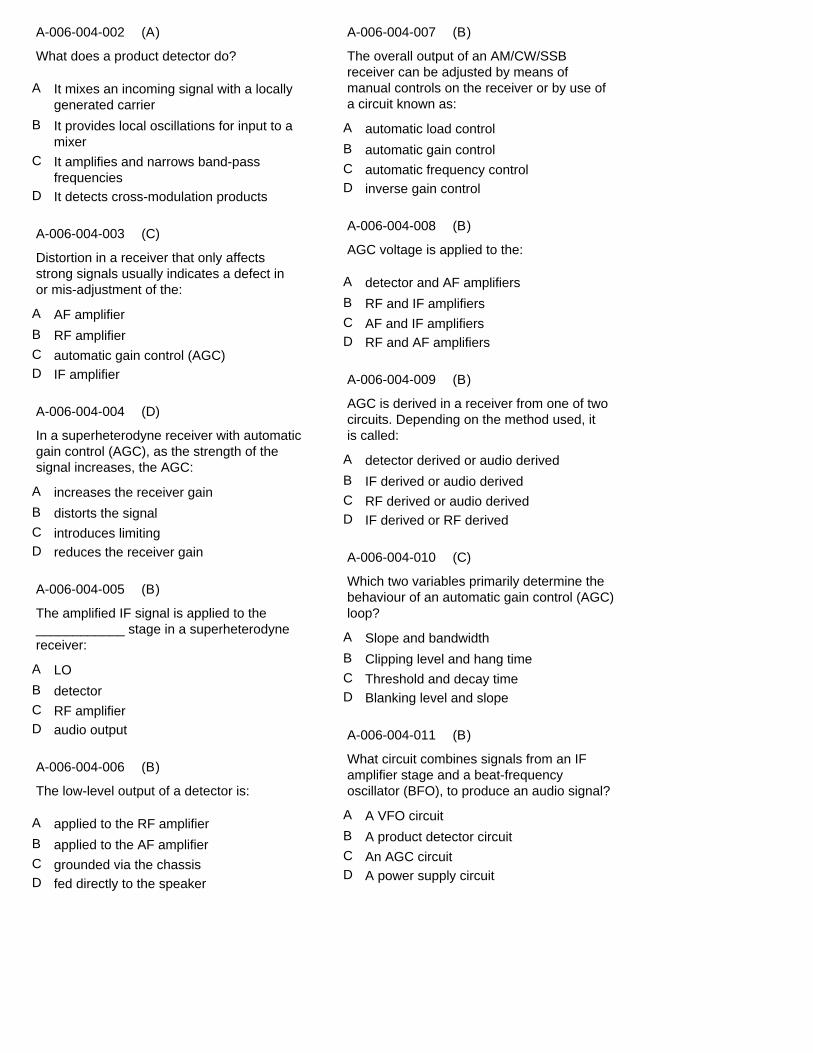
A-006-004-002
A-006-004-003
A-006-004-004
A-006-004-005
A-006-004-006
A-006-004-007
A-006-004-008
A-006-004-009
A-006-004-010
A-006-004-011
It mixes an incoming signal with a locallygenerated carrier
AF amplifier
increases the receiver gain
LO
applied to the RF amplifier
automatic load control
detector and AF amplifiers
detector derived or audio derived
Slope and bandwidth
A VFO circuit
It provides local oscillations for input to a mixer
RF amplifier
distorts the signal
detector
applied to the AF amplifier
automatic gain control
RF and IF amplifiers
IF derived or audio derived
Clipping level and hang time
A product detector circuit
It amplifies and narrows band-pass frequencies
automatic gain control (AGC)
introduces limiting
RF amplifier
grounded via the chassis
automatic frequency control
AF and IF amplifiers
RF derived or audio derived
Threshold and decay time
An AGC circuit
It detects cross-modulation products
IF amplifier
reduces the receiver gain
audio output
fed directly to the speaker
inverse gain control
RF and AF amplifiers
IF derived or RF derived
Blanking level and slope
A power supply circuit
What does a product detector do?
Distortion in a receiver that only affects strong signals usually indicates a defect in or mis-adjustment of the:
In a superheterodyne receiver with automaticgain control (AGC), as the strength of the signal increases, the AGC:
The amplified IF signal is applied to the ____________ stage in a superheterodyne receiver:
The low-level output of a detector is:
The overall output of an AM/CW/SSB receiver can be adjusted by means of manual controls on the receiver or by use of a circuit known as:
AGC voltage is applied to the:
AGC is derived in a receiver from one of two circuits. Depending on the method used, it is called:
Which two variables primarily determine the behaviour of an automatic gain control (AGC)loop?
What circuit combines signals from an IF amplifier stage and a beat-frequency oscillator (BFO), to produce an audio signal?
A
A
A
A
A
A
A
A
A
A
B
B
B
B
B
B
B
B
B
B
C
C
C
C
C
C
C
C
C
C
D
D
D
D
D
D
D
D
D
D
(A)
(C)
(D)
(B)
(B)
(B)
(B)
(B)
(C)
(B)

A-006-005-001
A-006-005-002
A-006-005-003
A-006-005-004
A-006-005-005
A-006-005-006
A-006-005-007
A-006-005-008
A-006-005-009
A-006-005-010
Product detector
Quieting
Strong near frequency signals
Increase the receiver bandwidth
Too little gain
To prevent the generation of spurious mixer products
the mixing of more than one signal in the first or second intermediate frequency amplifiers of a receiver
Feedback components
detector
Feedback
AGC loop
Desensitization
Squelch gain adjusted too high
Increase the transmitter audio gain
Positive feedback
To move the image response far away from the filter passband
the mixing of two or more signals in the front-end of a superheterodyne receiver
Temperature variations
RF amplifier
Desensitization
IF filter
Cross-modulation interference
Squelch gain adjusted too low
Use a cavity filter
Lack of neutralization
To provide a greater tuning range
the interaction of products from high-powered transmitters in the area
Dial display accuracy
mixer
Intermodulation
RF amplifier pre-selector
Squelch gain rollback
Audio gain adjusted too low
Decrease the receiver squelch gain
Nonlinear circuits or devices
To tune out cross-modulation distortion
the high-voltage stages in the final amplifier of an amplitude or frequency-modulated transmitter
Mechanical rigidity
local oscillator and power supply
Cross-modulation
What part of a superheterodyne receiver determines the image rejection ratio of the receiver?
What is the term for the reduction in receiversensitivity caused by a strong signal near the received frequency?
What causes receiver desensitization?
What is one way receiver desensitization can be reduced?
What causes intermodulation in an electronic circuit?
Which of the following is an important reason for using a VHF intermediate frequency in an HF receiver?
Intermodulation interference is produced by:
Which of the following is NOT a direct causeof instability in a receiver?
Poor frequency stability in a receiver usually originates in the:
Poor dynamic range of a receiver can cause many problems when a strong signal appears within or near the front-end bandpass. Which of the following is NOT caused as a direct result?
A
A
A
A
A
A
A
A
A
A
B
B
B
B
B
B
B
B
B
B
C
C
C
C
C
C
C
C
C
C
D
D
D
D
D
D
D
D
D
D
(D)
(B)
(A)
(C)
(D)
(B)
(B)
(C)
(D)
(A)

A-006-005-011
A-007-001-001
A-007-001-002
A-007-001-003
A-007-001-004
A-007-001-005
A-007-001-006
A-007-001-007
A-007-001-008
Two-tone Third-Order IMD Dynamic Range, 10 MHz spacing
The output is suitable for impedances from low to high
The circuit is known as a Series-type antenna tuner
The transmitter input is suitable for 50 ohms impedance
The transmitter input is suitable for impedance of 50 ohms
A network consisting of four inductors or four capacitors
Butterworth
It is prone to self-resonance
Network resistances substitute for load resistances
Third-Order Intercept Point
The circuit is known as a transformer-type antenna tuner
The output is suitable for impedances from low to high
The antenna output is high impedance
The antenna output is suitable for impedances from low to high
A power incidence network
L-network
It has limited power handling capability
It cancels the reactive part of an impedance and changes the resistive part
Blocking Dynamic Range
The circuit is known as a Pi-type antennatuner
The input is suitable for impedance of 50 ohms
The circuit is known as an L-type antenna tuner
The circuit is a Pi-type antenna tuner
A network consisting of one inductor and two capacitors or two inductors and one capacitor
Pi-network
It matches only a small impedance range
It produces transconductance to cancel the reactive part of an impedance
Intermediate frequency rejection ratio
The input is suitable for 50 ohm impedance
The circuit is known as a Pi-type antennatuner
The circuit is suitable for matching to a vertical ground plane antenna
The circuit is a series-type antenna tuner
An antenna matching network that is isolated from ground
Chebyshev
It is thermally unstable
It introduces negative resistance to cancel the resistive part of an impedance
Which of these measurements is a good indicator of VHF receiver performance in an environment of strong out-of-band signals?
For an antenna tuner of the "Transformer" type, which of the following statements is FALSE?
For an antenna tuner of the "Series" type, which of the following statements is false?
For an antenna tuner of the "L" type, which of the following statements is false?
For an antenna tuner of the "Pi" type, which of the following statements is false?
What is a pi-network?
Which type of network offers the greatest transformation ratio?
Why is an L-network of limited utility in impedance matching?
How does a network transform one impedance to another?
A
A
A
A
A
A
A
A
A
B
B
B
B
B
B
B
B
B
C
C
C
C
C
C
C
C
C
D
D
D
D
D
D
D
D
D
(A)
(C)
(D)
(D)
(D)
(C)
(C)
(C)
(B)
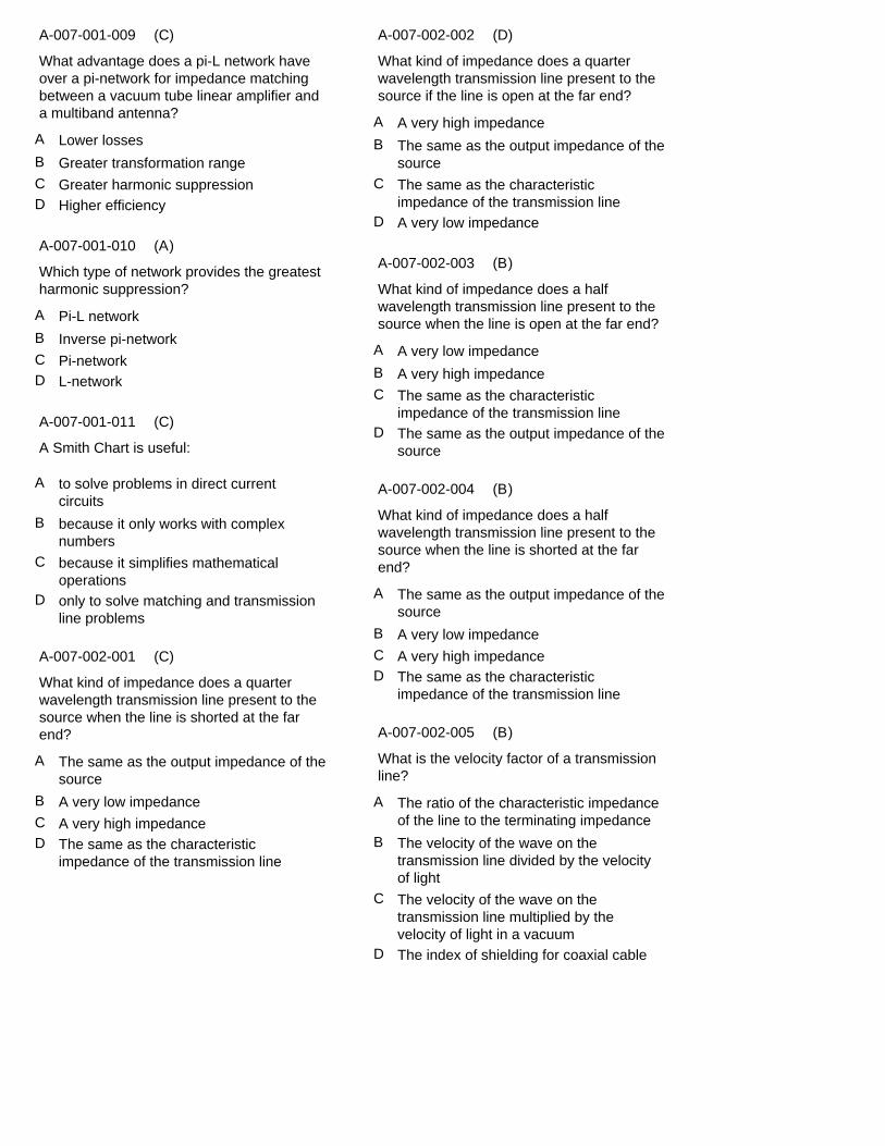
A-007-001-009
A-007-001-010
A-007-001-011
A-007-002-001
A-007-002-002
A-007-002-003
A-007-002-004
A-007-002-005
Lower losses
Pi-L network
to solve problems in direct current circuits
The same as the output impedance of thesource
A very high impedance
A very low impedance
The same as the output impedance of thesource
The ratio of the characteristic impedance of the line to the terminating impedance
Greater transformation range
Inverse pi-network
because it only works with complex numbers
A very low impedance
The same as the output impedance of thesource
A very high impedance
A very low impedance
The velocity of the wave on the transmission line divided by the velocity of light
Greater harmonic suppression
Pi-network
because it simplifies mathematical operations
A very high impedance
The same as the characteristic impedance of the transmission line
The same as the characteristic impedance of the transmission line
A very high impedance
The velocity of the wave on the transmission line multiplied by the velocity of light in a vacuum
Higher efficiency
L-network
only to solve matching and transmission line problems
The same as the characteristic impedance of the transmission line
A very low impedance
The same as the output impedance of thesource
The same as the characteristic impedance of the transmission line
The index of shielding for coaxial cable
What advantage does a pi-L network have over a pi-network for impedance matching between a vacuum tube linear amplifier and a multiband antenna?
Which type of network provides the greatest harmonic suppression?
A Smith Chart is useful:
What kind of impedance does a quarter wavelength transmission line present to the source when the line is shorted at the far end?
What kind of impedance does a quarter wavelength transmission line present to the source if the line is open at the far end?
What kind of impedance does a half wavelength transmission line present to the source when the line is open at the far end?
What kind of impedance does a half wavelength transmission line present to the source when the line is shorted at the far end?
What is the velocity factor of a transmission line?
A
A
A
A
A
A
A
A
B
B
B
B
B
B
B
B
C
C
C
C
C
C
C
C
D
D
D
D
D
D
D
D
(C)
(A)
(C)
(C)
(D)
(B)
(B)
(B)

A-007-002-006
A-007-002-007
A-007-002-008
A-007-002-009
A-007-002-010
A-007-002-011
A-007-003-001
A-007-003-002
A-007-003-003
Characteristic impedance
0.66
The line length
RF energy moves slower along the coaxial cable than in air
impedance
speed to which the standing waves are reflected back to the transmitter
The omega match
The stub match
The stub match
Surge impedance
0.33
The centre conductor resistivity
The surge impedance is higher in the parallel transmission line
hermetic losses
ratio of the velocity of propagation in the transmission line to the velocity of propagation in free space
The stub match
The T match
The omega match
Standing wave ratio
0.1
The terminal impedance
Skin effect is less pronounced in the coaxial cable
velocity factor
impedance of the line, e.g. 50 ohm, 75 ohm, etc.
The T match
The gamma match
The delta match
Velocity factor
2.7
Dielectrics in the line
The characteristic impedance is higher ina parallel transmission line
VSWR
speed at which the signal travels in free space
The gamma match
The omega match
The gamma match
What is the term for the ratio of the actual velocity at which a signal travels through a transmission line to the speed of light in a vacuum?
What is a typical velocity factor for coaxial cable with polyethylene dielectric?
What determines the velocity factor in a transmission line?
Why is the physical length of a coaxial cable shorter than its electrical length?
The reciprocal of the square root of the dielectric constant of the material used to separate the conductors in a transmission line gives the ____________ of the line:
The velocity factor of a transmission line is the:
What term describes a method used to match a high-impedance transmission line to a lower impedance antenna by connectingthe line to the driven element in two places, spaced a fraction of a wavelength on each side of the driven element centre?
What term describes an unbalanced feed system in which the driven element of an antenna is fed both at the centre and a fraction of a wavelength to one side of centre?
What term describes a method of antenna impedance matching that uses a short section of transmission line connected to the antenna transmission line near the antenna and perpendicular to the transmission line?
A
A
A
A
A
A
A
A
A
B
B
B
B
B
B
B
B
B
C
C
C
C
C
C
C
C
C
D
D
D
D
D
D
D
D
D
(D)
(A)
(D)
(A)
(C)
(B)
(C)
(C)
(A)

A-007-003-004
A-007-003-005
A-007-003-006
A-007-003-007
A-007-003-008
A-007-003-009
A-007-003-010
A-007-003-011
A-007-004-001
A-007-004-002
A-007-004-003
2.33 metres (7.64 feet)
gamma match
4 m (13.1 ft)
an "omega" match
the centre of the driven element
the coaxial line braid
the centre of the driven element
an adjustable point on the director
voltage
capacitance
maximum voltage
0.25 metre (0.82 foot)
lambda match
12 m (39.4 ft)
a "Y" match
the variable capacitor
the coaxial line centre conductor
the variable capacitor
center of the driven element
current
current
maximum current
3.51 metres (11.5 feet)
T match
8 m (26.2 ft)
a "gamma" match
the adjustable gamma rod
the adjustable gamma rod
the coaxial line centre conductor
coaxial line braid
inductance
voltage
minimum current
20 metres (65.6 feet)
zeta match
7.5 m (24.6 ft)
a "T" match
the centre of the reflector
a variable capacitor
an adjustable point on the reflector
adjustable gamma rod
capacitance
inductance
minimum voltage and current
Assuming a velocity factor of 0.66 what would be the physical length of a typical coaxial stub that is electrically one quarter wavelength long at 14.1 MHz?
The driven element of a Yagi antenna is connected to a coaxial transmission line. The coax braid is connected to the centre of the driven element and the centre conductor is connected to a variable capacitor in serieswith an adjustable mechanical arrangement on one side of the driven element. The type of matching is:
A quarter-wave stub, for use at 15 MHz, is made from a coaxial cable having a velocity factor of 0.8. Its physical length will be:
The matching of a driven element with a single adjustable mechanical and capacitive arrangement is descriptive of:
A Yagi antenna uses a gamma match. The coaxial braid connects to:
A Yagi antenna uses a gamma match. The centre of the driven element connects to:
A Yagi antenna uses a gamma match. The adjustable gamma rod connects to:
A Yagi antenna uses a gamma match. The variable capacitor connects to the:
In a half-wave dipole, the distribution of _______ is highest at each end.
In a half-wave dipole, the distribution of _______ is lowest at each end.
The feed point in a centre-fed half-wave antenna is at the point of:
A
A
A
A
A
A
A
A
A
A
A
B
B
B
B
B
B
B
B
B
B
B
C
C
C
C
C
C
C
C
C
C
C
D
D
D
D
D
D
D
D
D
D
D
(C)
(A)
(A)
(C)
(A)
(A)
(B)
(D)
(A)
(B)
(B)

A-007-004-004
A-007-004-005
A-007-004-006
A-007-004-007
A-007-004-008
A-007-004-009
A-007-004-010
A-007-004-011
A-007-005-001
A-007-005-002
A-007-005-003
voltage
current
the current is maximum
voltage is low and current is high
voltage and current are both high
Both ends
At the right end
At the centre
Waves with a rotating electric field
Circular polarization
Lindenblad antenna
capacity
inductance
the voltage is maximum
voltage is high and current is low
voltage and current are both low
The centre
At both ends
It is the same at all points
Waves with an electric field bent into circular shape
Cross-polarization
Axial-mode helical antenna
inductance
voltage
the resistance is maximum
voltage and current are both high
voltage is high and current is low
At the right end
At the centre
At the right end
Waves that circle the earth
Perpendicular polarization
Loaded helical-wound antenna
current
capacity
the antenna is resonant
voltage and current are both low
voltage is low and current is high
It is equal at all points
It is equal at all points
At both ends
Waves produced by a circular loop antenna
None of the other answers, the two fields cancel out
Crossed dipoles fed 90 degrees out of phase
In a half-wave dipole, the lowest distribution of _________ occurs at the middle.
In a half-wave dipole, the highest distribution of ________ occurs at the middle.
A half-wave dipole antenna is normally fed atthe point where:
At the ends of a half-wave dipole:
The impedance of a half-wave antenna at its centre is low, because at this point:
In a half-wave dipole, where does minimum voltage occur?
In a half-wave dipole, where does the minimum current occur?
In a half-wave dipole, where does the minimum impedance occur?
What is meant by circularly polarized electromagnetic waves?
What type of polarization is produced by crossed dipoles fed 90 degrees out of phase?
Which of these antennas does not produce circular polarization?
A
A
A
A
A
A
A
A
A
A
A
B
B
B
B
B
B
B
B
B
B
B
C
C
C
C
C
C
C
C
C
C
C
D
D
D
D
D
D
D
D
D
D
D
(A)
(A)
(A)
(B)
(D)
(B)
(B)
(A)
(A)
(A)
(C)

A-007-005-004
A-007-005-005
A-007-005-006
A-007-005-007
A-007-005-008
A-007-005-009
A-007-005-010
A-007-005-011
A-007-006-001
A-007-006-002
Contact via satellite
10 dB
Offset feed
a horn-type radiator can be used to trap the received energy
vertical polarization only
quad antenna
0.25 lambda
the focal length of the antenna
400 watts
high antenna voltage
Contact through a hilltop repeater
20 dB or more
Cassegrain
all the received energy is focused to a point where the pick-up antenna is located
horizontal polarization
helical-beam antenna
5 mm (0.2 in) regardless of frequency
the material composition of the dish
300 watts
leakage to ground through the dielectric
Simplex line-of-sight contact between hand-held transceivers
3 dB
Newtonian
a dipole antenna can be used to pick up the received energy
right-hand polarization
folded dipole antenna
1% of the diameter
the diameter of the antenna in wavelengths
200 watts
dielectric and conductor heat losses
Contact with terrestrial mobile stations
6 dB
Front feed
no impedance matching is required
left-hand polarization
ground-plane antenna
0.1 lambda
the polarization of the feed device illuminating it
350 watts
high antenna currents
On VHF/UHF frequencies, Doppler shift becomes of consequence on which type of communication?
For VHF and UHF signals over a fixed path, what extra loss can be expected when linearly-polarized antennas are crossed-polarized (90 degrees)?
Which of the following is NOT a valid parabolic dish illumination arrangement?
A parabolic antenna is very efficient because:
A helical-beam antenna with right-hand polarization will best receive signals with:
One antenna which will respond simultaneously to vertically- and horizontally-polarized signals is the:
In amateur work, what is the surface error upper limit you should try not to exceed on aparabolic reflector?
You want to convert a surplus parabolic dishfor amateur radio use, the gain of this antenna depends on:
A transmitter has an output of 100 watts. The cable and connectors have a composite loss of 3 dB, and the antenna has a gain of 6 dBd. What is the Effective Radiated Power?
As standing wave ratio rises, so does the loss in the transmission line. This is caused by:
A
A
A
A
A
A
A
A
A
A
B
B
B
B
B
B
B
B
B
B
C
C
C
C
C
C
C
C
C
C
D
D
D
D
D
D
D
D
D
D
(A)
(B)
(C)
(B)
(C)
(B)
(D)
(C)
(C)
(C)

A-007-006-003
A-007-006-004
A-007-006-005
A-007-006-006
A-007-006-007
A-007-006-008
A-007-006-009
A-007-006-010
390 watts
power supplied to the transmission line plus antenna gain
3200 watts
100 watts
remain the same
1125
6
18 000
197 watts
ratio of signal output power to signal inputpower
1600 watts
200 watts
be cut in half
134
1.5
20 000
228 watts
transmitter output power, minus line losses, plus antenna gain relative to a dipole
400 watts
800 watts
double
1000
2
2009
178 watts
power supplied to the antenna before the modulation of the carrier
800 watts
400 watts
decrease by 3 watts
1250
4
16 000
What is the Effective Radiated Power of an amateur transmitter, if the transmitter outputpower is 200 watts, the transmission line loss is 5 watts, and the antenna power gain is 3 dBd?
Effective Radiated Power means the:
A transmitter has an output power of 200 watts. The coaxial and connector losses are3 dB in total, and the antenna gain is 9 dBd.What is the approximate Effective Radiated Power of this system?
A transmitter has a power output of 100 watts. There is a loss of 1.30 dB in the transmission line, a loss of 0.2 dB through the antenna tuner, and a gain of 4.50 dBd in the antenna. The Effective Radiated Power (ERP) is:
If the overall gain of an amateur station is increased by 3 dB the ERP (Effective Radiated Power) will:
A transmitter has a power output of 125 watts. There is a loss of 0.8 dB in the transmission line, 0.2 dB in the antenna tuner, and a gain of 10 dBd in the antenna. The Effective Radiated Power (ERP) is:
If a 3 dBd gain antenna is replaced with a 9 dBd gain antenna, with no other changes, the Effective Radiated Power (ERP) will increase by:
A transmitter has an output of 2000 watts PEP. The transmission line, connectors andantenna tuner have a composite loss of 1 dB, and the gain from the stacked Yagi antenna is 10 dBd. What is the Effective Radiated Power (ERP) in watts PEP?
A
A
A
A
A
A
A
A
B
B
B
B
B
B
B
B
C
C
C
C
C
C
C
C
D
D
D
D
D
D
D
D
(A)
(C)
(D)
(B)
(C)
(C)
(D)
(D)

A-007-006-011
A-007-007-001
A-007-007-002
A-007-007-003
A-007-007-004
A-007-007-005
A-007-007-006
A-007-007-007
8000
It increases with increasing height
an eighth of a wavelength above the ground
at ground level exactly
It uses vertical polarization
radiation pattern is unaffected
Antenna height has no effect on the pattern
more than 45 degrees but less than 90 degrees
1009
It does not vary with height
a quarter wavelength above the ground
several centimeters to as much as 2 meters below ground, depending upon soil conditions
The vertical radiation angle is lower
vertical or upward radiation is effectively cancelled
If the antenna is less than one-half wavelength high, radiation off the ends of the wire is eliminated
90 degrees
10 000
It depends on E-region height, not antenna height
three-eighths of a wavelength above the ground
as much as 6 cm below ground depending upon soil conditions
The radiation resistance is lower
radiation pattern changes to produce sidelobes at 15 and 50 degrees
If the antenna is too high, the pattern becomes unpredictable
more than 30 degrees but less than 45 degrees
9000
It decreases with increasing height
a half wavelength or more above the ground
as much as a meter above ground
It has an omnidirectional characteristic
side lobe radiation is cancelled
If the antenna is less than one-half wavelength high, reflected radio waves from the ground significantly distort the pattern
less than 30 degrees
A transmitter has an output of 1000 watts PEP. The coaxial cable, connectors and antenna tuner have a composite loss of 1 dB, and the antenna gain is 10 dBd. What isthe Effective Radiated Power (ERP) in watts PEP?
For a 3-element Yagi antenna with horizontally mounted elements, how does the main lobe takeoff angle vary with height above flat ground?
Most simple horizontally polarized antennas do not exhibit significant directivity unless they are:
The plane from which ground reflections can be considered to take place, or the effective ground plane for an antenna is:
Why is a ground-mounted vertical quarter-wave antenna in reasonably open surroundings better for long distance contacts than a half-wave dipole at a quarter wavelength above ground?
When a half-wave dipole antenna is installedone-half wavelength above ground, the:
How does antenna height affect the horizontal (azimuthal) radiation pattern of a horizontal dipole HF antenna?
For long distance propagation, the vertical radiation angle of the energy from the antenna should be:
A
A
A
A
A
A
A
A
B
B
B
B
B
B
B
B
C
C
C
C
C
C
C
C
D
D
D
D
D
D
D
D
(A)
(D)
(D)
(B)
(B)
(B)
(D)
(D)

A-007-007-008
A-007-007-009
A-007-007-010
A-007-007-011
A-007-008-001
A-007-008-002
A-007-008-003
A-007-008-004
length of the antenna
75 ohms
Lower antenna noise temperature
A vertical antenna and a frequency above the lowest usable frequency
The equivalent resistance that would dissipate the same amount of power as that radiated from an antenna
To calculate the front-to-back ratio of the antenna
Transmission line length and antenna height
Antenna efficiency
vertical radiation angle of the antenna
25 ohms
Low radiation angle for closer distances
A horizontal antenna less than 1/4 wavelength above ground and a frequencybelow the current critical frequency
The resistance in the atmosphere that anantenna must overcome to be able to radiate a signal
To match impedances for maximum power transfer
Sunspot activity and time of day
Beamwidth
power applied to the antenna
300 ohms
The radiation resistance is higher
A horizontal antenna at a height of half a wavelength and an operating frequency atthe optimum working frequency
The specific impedance of an antenna
To measure the near-field radiation density from a transmitting antenna
It is a physical constant and is the same for all antennas
Effective Radiated Power
main height of the antenna
600 ohms
The ground tends to act as a reflector
A vertical antenna and a frequency below the maximum usable frequency
The combined losses of the antenna elements and transmission line
To calculate the front-to-side ratio of the antenna
Antenna location with respect to nearby objects and the conductors length/diameter ratio
Radiation conversion loss
Greater distance can be covered with multiple-hop transmissions by decreasing the:
The impedance at the centre of a dipole antenna more than 3 wavelengths above ground would be nearest to:
Why can a horizontal antenna closer to ground be advantageous for close range communications on lower HF bands?
Which antenna system and operating frequency are most suitable for Near VerticalIncidence (NVIS) communications?
What is meant by the radiation resistance ofan antenna?
Why would one need to know the radiation resistance of an antenna?
What factors determine the radiation resistance of an antenna?
What is the term for the ratio of the radiationresistance of an antenna to the total resistance of the system?
A
A
A
A
A
A
A
A
B
B
B
B
B
B
B
B
C
C
C
C
C
C
C
C
D
D
D
D
D
D
D
D
(B)
(A)
(D)
(B)
(A)
(B)
(D)
(A)

A-007-008-005
A-007-008-006
A-007-008-007
A-007-008-008
A-007-008-009
A-007-008-010
A-007-008-011
A-007-009-001
A-007-009-002
Radiation resistance plus transmission resistance
Note the two points where the signal strength is down 3 dB from the maximumsignal point and compute the angular difference
(radiation resistance / total resistance) x 100
K factor
the points on the major lobe at the half-power points
72%
52%
at frequencies above 3000 MHz
low copper loss
Transmission line resistance plus radiation resistance
Draw two imaginary lines through the ends of the elements and measure the angle between the lines
(radiation resistance / transmission resistance) x 100
Radiation resistance
the maximum lobe spread points on the major lobe
100%
25%
at frequencies above 2 MHz
low hysteresis loss
Radiation resistance plus space impedance
Measure the ratio of the signal strengths of the radiated power lobes from the front and side of the antenna
(total resistance / radiation resistance) x 100
j factor
the 6 dB power points on the major lobe
97.3%
50%
at frequencies below 150 MHz
low radiation loss
Radiation resistance plus ohmic resistance
Measure the ratio of the signal strengths of the radiated power lobes from the front and rear of the antenna
(effective radiated power / transmitter output) x 100
Antenna resistance
the 3 dB power points on the first minor lobe
74%
96.15%
at frequencies below 1500 MHz
low dielectric loss
What is included in the total resistance of anantenna system?
How can the approximate beamwidth of a beam antenna be determined?
How is antenna percent efficiency calculated?
What is the term used for an equivalent resistance which would dissipate the same amount of energy as that radiated from an antenna?
Antenna beamwidth is the angular distance between:
If the ohmic resistance of a half-wave dipole is 2 ohms, and the radiation resistance is 72ohms, what is the antenna efficiency?
If the ohmic resistance of a miniloop antennais 2 milliohms and the radiation resistance is50 milliohms, what is the antenna efficiency?
Waveguide is typically used:
Which of the following is not correct? Waveguide is an efficient transmission medium because it features:
A
A
A
A
A
A
A
A
A
B
B
B
B
B
B
B
B
B
C
C
C
C
C
C
C
C
C
D
D
D
D
D
D
D
D
D
(D)
(A)
(A)
(B)
(A)
(C)
(D)
(A)
(B)

A-007-009-003
A-007-009-004
A-007-009-005
A-007-009-006
A-007-009-007
A-007-009-008
A-007-009-009
A-007-009-010
A-007-009-011
Frequency sensitive based on dimensions
three-eighths wavelength
In the transverse electric mode, a component of the magnetic field is in the direction of propagation
Easy to install
Microstripline
has poorer shielding
operates like a low-pass filter
family of fluids for removing coatings fromsmall parts
Be sure propagation conditions are unfavourable for tropospheric ducting
Expensive
one-eighth wavelength
In the transverse magnetic mode, a component of the electric field is in the direction of propagation
Inexpensive to install
Dielectric substrate
has superior shielding
operates like a band-stop filter
printed circuit transmission line
Be sure to wear tight-fitting clothes and gloves to protect your body and hands from sharp edges
Heavy and difficult to install
one-quarter wavelength
Waveguide has low loss at high frequencies, but high loss below cutoff frequency
Very low losses
Dielectric imprinting
must have much lower characteristic impedance
is lightweight and easy to install
small semiconductor family
Be sure the transmitter is turned off and the power source is disconnected
Low loss
one-half wavelength
Waveguide has high loss at high frequencies, but low loss below cutoff frequency
Frequency response from 1.8 MHz to 24GHz
Ground plane
must have much higher characteristic impedance
operates like a high-pass filter
high power microwave antenna
Be sure the weather is dry and sunny
Which of the following is an advantage of waveguide as a transmission line?
For rectangular waveguide to transfer energy, the cross-section should be at least:
Which of the following statements about waveguide IS NOT correct?
Which of the following is a major advantage of waveguide over coaxial cable for use at microwave frequencies?
What is printed circuit transmission line called?
Compared with coaxial cable, microstripline:
A section of waveguide:
Stripline is a:
What precautions should you take before beginning repairs on a microwave feed horn or waveguide?
A
A
A
A
A
A
A
A
A
B
B
B
B
B
B
B
B
B
C
C
C
C
C
C
C
C
C
D
D
D
D
D
D
D
D
D
(D)
(D)
(D)
(C)
(A)
(A)
(D)
(B)
(C)