Embed Size (px)
Citation preview

IEEE TRANSACTIONS ON ELECTRON DEVICES, VOL. 49, NO. 3, MARCH 2002 457
Advanced Model and Analysis of Series Resistancefor CMOS Scaling Into Nanometer Regime—Part I:
Theoretical DerivationSeong-Dong Kim, Member, IEEE, Cheol-Min Park, Member, IEEE, and Jason C. S. Woo, Senior Member, IEEE
Abstract—An advanced series resistance model is developedto accurately predict source/drain (S/D) series resistance ofcomplementary metal-oxide semiconductor (CMOS) in thenanometer regime. The series resistance is modeled by dividinginto four resistance components named SDE-to-gate overlap,S/D extension, deep S/D, and silicide-diffusion contact resistanceconsidering the nonnegligible doping-dependent potential re-lationship in MOS accumulation region due to scaled supplyvoltage, current behavior related to heavily doped ultra-shallowsource/drain extension (SDE) junction, polysilicon gate depletioneffects (PDE), lateral and vertical doping gradient effect ofSDE junction, silicide-diffusion contact structure, and high-dielectric sidewall. The proposed model well characterizes uniquefeatures of nanometer-scale CMOS and is useful for analyzing theeffect of source/drain parameters on CMOS device scaling andoptimization.
Index Terms—CMOS, high-k dielectrics, modeling, polysilicongate depletion effect, scaling, series resistance, specific contact re-sistivity, transmission line model, ultra-shallow junction.
I. INTRODUCTION
DUE to the considerable progress of CMOS technologyover the last two decades, scaling technology and de-
vice dimensions are approaching the fundamental physicallimitation of the nanometer regime [1], [2]. The internationaltechnology roadmap for semiconductor (ITRS) roadmap [3]predicts that the source/drain extension junction depth belowsub-50 nm CMOS will be scaled further down around 10 nmto maintain acceptable short channel performance, but thismay lead to a high series resistance problem threatening theultimate device performance. Since source/drain engineeringof nanoscale CMOS for achieving low parasitic source/drainseries resistance as well as ultrashallow SDE junction is verydifficult and challenging technology, there is an increasing con-cern about the series resistance that may be a serious limitingfactor for CMOS scaling into nanometer regime [4]–[6].
In order to minimize the series resistance and optimizethe source/drain structure, it is essential to understand therelative contribution of resistance components on the totalseries resistance and their dependence on the device/processparameters prior to selecting the values of process/deviceparameters such as implantation dose and energy, temperature
Manuscript received April 23, 2001; revised November 19, 2001. The reviewof this paper was arranged by Editor K. Shenai.
The authors are with the Department of Electrical Engineering, University ofCalifornia, Los Angeles, CA 90095 USA (e-mail: [email protected]).
Publisher Item Identifier S 0018-9383(02)02113-5.
budget, source/drain junction dimension, and silicide contactparameters.
There have been many reports about the modeling and anal-ysis on the S/D series resistance [5], [7]. However, most of themodels have not considered the extremely short channel de-vice structures, which have parameters of less important in theabove sub-100 nm CMOS regime, so that these models fail toaccurately predict and analyze the series resistance as devicesbecome scaled down below 100 nm. Also, the analysis onlythrough the simulation is difficult to not only separate the S/Dstructure regionally but also provide physical insight of deviceparameters directly.
In this work, we present an advanced series resistance model,which allows us to describe unique features of nanoscale CMOSsuch as a scaled supplied voltage approaching 1.0 V or less,ultrashallower source drain extension (SDE) junction structurewith higher doping concentration, polysilicon gate depletion ef-fects (PDE), lateral and vertical doping gradient effect in SDEjunction, relatively enlarged sidewall length, silicide-diffusioncontact system, and high-dielectric sidewall effect.
II. M ODELING
The process and device simulations were performed usingSILVACO simulation tools. The contours of conduction cur-rent density and doping concentration of 70 nm gate lengthNMOSFET operated at the triode region are depicted in Fig. 1where the contour of minimum current density is zero and itsincrement is 1.25 10 A/cm . As shown in Fig. 1, the cur-rent density contours show that most of the surface channel cur-rent flowing through the accumulation layer spread out into thewhole neutral SDE junction region outside the depletion regionboundary and the portions of depletion width and silicide-diffu-sion contact system in the SDE and deep junction are relativelyenlarged owing to shallower and smaller junction geometry.
Fig. 2 describes schematic representation of S/D structure andits equivalent circuit for use in modeling the series resistance.The series resistance can be divided into the four components,overlap resistance ; extension resistance ; deep resis-tance ; and silicide-diffusion contact resistance . Eachresistance component consists of the parallel or series combina-tions of subresistance components according to the carrier con-duction path and doping profiles.
In the regime of below 100 m channel lengths, the excessivelyhigher doping concentrations in the SDE and deep junction re-
0018–9383/02$17.00 © 2002 IEEE

458 IEEE TRANSACTIONS ON ELECTRON DEVICES, VOL. 49, NO. 3, MARCH 2002
Fig. 1. Contours of conduction current density and doping concentration of70 nm gate length NMOSFET under triode region operation where the contourof minimum current density is zero and the increment is 1.25�10 A/cm .The characteristics of ultrashallow S/D junction structure such as the increasedportion of depletion width, current flow spreading outside depletion boundary,and a relatively enlarged silicide-diffusion contact system can be observed.
Fig. 2. Schematic representation of source/drain structure for use in modelingof series resistance and its equivalent circuit.
gion are expected between 10and 10 cm , and these crit-ical high-doping ranges are difficult to fit with a simple powerfunction to get an accurate bulk mobility as a function of thedoping concentration. Therefore, the general empirical bulk mo-bility model that covers entire doping range was used in thismodel [8].
In addition to bulk mobility, the impact of the accumulationlayer mobility model is increasingly important as the device isscaled below 100 nm gate length. The scattering mechanismsof the accumulation layer such as screened Coulomb scattering
at low transverse field region and the carrier-carrier scatteringdue to ionized impurities are different from that of the inver-sion layer and should be properly modeled in the overlap layerresistance to increase the accuracy of the model [9], [10]. Weemployed the universal channel carrier mobility model whosecoefficients are adjusted to the experimental data of the accu-mulation layer with high-doping levels [10], [11].
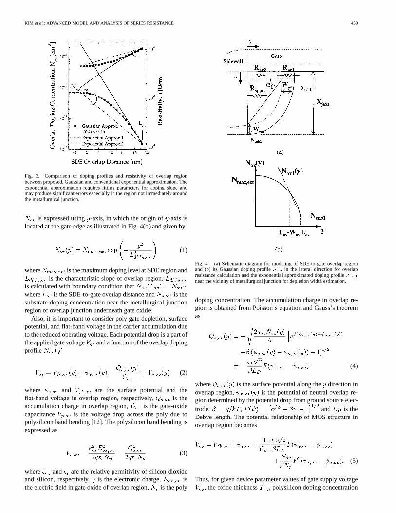
A. SDE-to-Gate Overlap Resistance
The percentage of SDE-to-gate overlap length in the gatelength is increasing up to 30 40% as the technology shrinksdown, making the overlap resistance more important andbias dependent. The doping concentration in overlap regionis closely related to overlap resistance, because the currentspreading takes place due to the unavoidable doping gradientand hence wider conduction paths and the accumulation carriercharge density is dependent on the overlap doping concentra-tion. Furthermore, since the lateral slope of overlap dopingprofile is much more critical for controlling the short channeleffect as well as the device performance in the nanometerregime, proper care should be taken with respect to the lateraldoping gradient in overlap region for accurately estimating theoverlap resistance and optimizing its structure [4], [5].
Most of the previous series resistance models and analyseshave assumed the exponentially sloped doping profile and theconstant accumulation charge density in the overlap region [5],[7]. This is because the exponentially sloped doping profileis simple and easy to derive the analytical formula. However,the exponential doping profile requires fitting parameters foradjusting doping slope and may be applicable only near thevicinity of the metallurgical junction, so that it may producesignificant errors especially in the region not immediatelyaround the metallurgical junction as shown in Fig. 3. Moreover,the assumption of constant surface accumulation charge densityby neglecting the doping-dependent surface potential varia-tion considerably underestimate the overlap resistance in thenanoscale CMOS with the scaled supply voltage approaching1.0 V or less.
In this model, one-dimensional (1-D) Gaussian doping gra-dient is assumed in the lateral direction of overlap region wherecurrent accumulation and spreading occur. The vertical dopinggradient is not important because most of the accumulation andspreading current are occurred due to the lateral doping gradientof overlap junction as shown in Fig. 1.
The device has an accumulation layer in the entire surfaceunder gate oxide in the overlap region although there may be adistant range where the induced carrier density is smaller thanthe background doping level in the overlap region. Also, sincethe SDE regions of nanoscale devices are very shallow junctionwith high doping level and relatively large depletion width, thecurrent spreading can be assumed to start to flow into the neu-tral bulk region out of the depletion boundary of SDE/substratejunction as is observed from the simulated current density con-tour in Fig. 1. As a result, the overlap resistance can be mod-eled by the series and parallel combination of , , and
, as shown in Fig. 4(a). The overlap doping concentration,
KIM et al.: ADVANCED MODEL AND ANALYSIS OF SERIES RESISTANCE 459
Fig. 3. Comparison of doping profiles and resistivity of overlap regionbetween proposed, Gaussian and conventional exponential approximation. Theexponential approximation requires fitting parameters for doping slope andmay produce significant errors especially in the region not immediately aroundthe metallurgical junction.
is expressed using-axis, in which the origin of -axis islocated at the gate edge as illustrated in Fig. 4(b) and given by
(1)
where is the maximum doping level at SDE region andis the characteristic slope of overlap region.
is calculated with boundary condition thatwhere is the SDE-to-gate overlap distance and is thesubstrate doping concentration near the metallurgical junctionregion of overlap junction underneath gate oxide.
Also, it is important to consider poly gate depletion, surfacepotential, and flat-band voltage in the carrier accumulation dueto the reduced operating voltage. Each potential drop is a part ofthe applied gate voltage and a function of the overlap dopingprofile
(2)
where and are the surface potential and theflat-band voltage in overlap region, respectively, is theaccumulation charge in overlap region, is the gate-oxidecapacitance is the voltage drop across the poly due topolysilicon band bending [12]. The polysilicon band bending isexpressed as
(3)
where and are the relative permitivity of silicon dioxideand silicon, respectively, is the electronic charge, isthe electric field in gate oxide of overlap region, is the poly
Fig. 4. (a) Schematic diagram for modeling of SDE-to-gate overlap regionand (b) its Gaussian doping profileN in the lateral direction for overlapresistance calculation and the exponential approximated doping profileN
near the vicinity of metallurgical junction for depletion width estimation.
doping concentration. The accumulation charge in overlap re-gion is obtained from Poisson’s equation and Gauss’s theoremas
(4)
where is the surface potential along thedirection inoverlap region, is the potential of neutral overlap re-gion determined by the potential drop from ground source elec-trode, , and is theDebye length. The potential relationship of MOS structure inoverlap region becomes
(5)
Thus, for given device parameter values of gate supply voltage, the oxide thickness , polysilicon doping concentration

460 IEEE TRANSACTIONS ON ELECTRON DEVICES, VOL. 49, NO. 3, MARCH 2002
, and overlap-doping concentration , the surface po-tential can be determined with simple numerical iteration.The accumulation carrier density, is obtained as a functionof overlap distance or overlap doping profile by
(6)Accordingly, the resistance components of accumulation layer,
and become as shown in (7) and (8) at the bottom ofthe page. (see also (8), shown at the bottom of the page). respec-tively, where is the universal channel accumulation carriermobility whose model coefficients are adjusted to accumulationlayer as mentioned earlier [10], [11].
As can be seen in Fig. 4, the current spreading is mod-eled based on the depletion approximation. To calculate thespreading resistance, we should find the depletion widths andspreading angle. There are two depletion widths in overlapregion as indicated in Fig. 4. is the depletion width inoverlap region near the surface overlap/channel metallurgicaljunction under the gate oxide and is the depletion widthnear the vertically diffused SDE junction depth. They can befound from the iterative solution with the simplified expressionof the diffusion profile having exponential slope that is gov-erned only near the vicinity of the junctions (see Appendix A).They also determine the current spreading angleby
(9)
where and are SDE junction depth and approximatedaccumulation layer thickness [7], respectively. Most of the pre-vious models assumed that the current spreads within the fixedspreading angle for all S/D structures. In practice, however, thecurrent spreading depends on the variation of depletion widthsand junction geometry as modeled in (9), e.g., the shallower andthe longer SDE-to-gate overlap, the smaller spreading angle.Therefore, this model is useful for characterizing various ge-ometry and doping profile.
The incremental spreading resistance can be interpreted as
(10)
and from the assumption that the current diverges withspreading angle as
(11)
the expression of the spreading resistance can be derivedas
(12)
where is the resistivity in the overlap region. The ischanged by the doping concentration and correspondingbulk mobility along the overlap distance and given by
(13)
B. Source/Drain Extension Resistance
The modeling of the S/D extension resistance is depicted inFig. 5(a) and (b). The axis is defined from the SDE junc-tion to the contact region and its origin is at the gate corner edgepoint as shown Fig. 5(a). The surface region of the extension anddeep region can be modulated by high fringing field from thegate edge, which would be pronounced in the future ultra smalldevice with possible use of the high-dielectric sidewall [13].In this model, the fringing resistance inserted in parallel withthe extension resistance is taken into account to characterize thefringing field effect on the surface extension region as shown inFig. 5(a). Using approximation of the uniform potential alongthe gate edge region and SDE surface region, the fringing ca-pacitance in the extension region, is obtained throughconformal transformation given in Appendix C [14]. Then, thefringing resistance in SDE region can be calculated by iterativesolution of the potential relationship of gate/sidewall/Si systemwhich is similar to accumulation calculation and given by
(14)
where and are the sidewall length and the deep regionlength, respectively, is the accumulation carrier density
(7)
(8)

KIM et al.: ADVANCED MODEL AND ANALYSIS OF SERIES RESISTANCE 461
Fig. 5. (a) Schematic diagram for modeling of S/D extension region and (b)its Gaussian doping profile in the vertical direction for extension resistancecalculation.
in the extension region induced by fringing field is themobility of the accumulation carrier induced by fringing field
and are the surface potential and the flat-bandvoltage in extension region, respectively, is the voltagedrop across the poly due to PDE.
The uniform doping concentration of is defined inthe surface extension region within and subsequently, theGaussian diffusion, is assumed after uniform doping region fordescribing junction tailing profile caused by transient enhanceddiffusion (TED) as shown in Fig. 5(b). Accordingly, the dopingconcentration of the extension region is described by
for
for (15)
where are the vertical characteristic slope of theextension region obtained from the boundary condition of
where is the SDE junctiondepth and is substrate doping concentration underneathSDE junction. The surface resistance in the extension region,
is easily obtained from the approximation of uniformdoping region within
(16)
where is the resistivity in the surface uniform doping regionof the extension junction.
The spreading resistance in the extension region, canbe modeled by vertically graded Gaussian doping profile andspreading angle with the approximated depletion width cal-culation of (see Appendix B)
(17)
where is
(18)
C. Deep Source/Drain Resistance
The lateral diffusion from the sidewall edge of deep S/D im-plantation forms the S/D deep region as shown in Fig. 2(a). Thecontribution of the deep resistance is relatively small in the totalseries resistance because of the heavily doped deep junction. Weemployed the average doping and the same spreading angle with
in the calculation of the deep resistance for simplicity as il-lustrated in Fig. 6.
The modulation effect of the gate fringing field is negligiblein the surface deep region because practically, the deep regionis relatively long from gate edge as well as too heavily doped tobe modulated. The lateral encroachment of the silicide,is included in the surface resistance of the deep region, sinceit may not be ignored in the deep submicron MOSFET withrelatively large silicide area in shallower junction. The surfaceresistance in the deep region, is the reciprocal of theconductance obtained by integrating conductor segment fromsurface to silicide depth as follows:
(19)
where is the resistivity of the deep region calculated by theaverage doping concentration and is silicide thickness.
The spreading resistance in the deep region, is ob-tained from the assumption of the identical spreading angle withthe extension region as in (20), shown at the bottom of the nextpage.
D. Silicide-Diffusion Contact Resistance
The silicide-diffusion contact resistance is defined as the re-sistance between the silicide contact and the diffusion layer un-derneath the silicide layer. It strongly depends on the silicidethickness, the doping concentration of deep junction region andthe silicide material, because the specific contact resistivity is

462 IEEE TRANSACTIONS ON ELECTRON DEVICES, VOL. 49, NO. 3, MARCH 2002
Fig. 6. (a) Schematic diagram for modeling of deep S/D region and (b) itsradial doping profile for depletion width estimation.
determined by the active dopant concentration at the silicide/Siinterface, and Schottky barrier height as is given by [15]
(21)
where and are physical constants. can be obtainedfrom the Gaussian approximation of the deep junction dopingconcentration in vertical direction and is described by
(22)
where is maximum doping concentration in deep junc-tion, is peak location of the deep doping concentration,
is the vertical characteristic slope of the deep regionobtained in similar manner to SDE region.
Much work has been done on the analysis of self-aligned sili-cide contact structure and reported that the 1-D transmission line
model (1-D-TLM) is useful and simple method to accurately de-scribe the behavior of the silicide contact resistance even in thenanoscale dimensions [16]–[18]. We adopted 1-D-TLM for an-alyzing the effect of silicide parameters such as silicide thick-ness, deep junction doping concentration, and Schottky barrierheight on the series resistance. The silicide-diffusion contact re-sistance, can be expressed as
(23)
where is the effective contact length in the silicide contact,is the contact transfer length defined as
where is the diffusion sheet resistance underneath silicidelayer. It can be seen in the simulation that the silicide-diffusioncontact structure has an additional current path at the side ofrecessed contact region being parallel with current flow at thecontact under the silicide layer. However, although this currentflow increases with the increase of the silicide thickness due tothe increase of sidewall contact area, it has been reported that asignificant amount of current is still pushed into the lower partof silicon region under the silicide [18]. Hence, the sidewall con-tact resistance has a minor effect on the total silicide-diffusioncontact resistance and we exclude this side current effect in themodeling of silicide-diffusion contact resistance to eliminate theadditional unexpected error.
E. Total Series Resistance
The total series resistance can be expressed by the summa-tion of four series resistance components and each resistancecomponent comprises its parallel or series subresistance com-ponents as follows
(24)
III. A PPLICATION TO SUB-100 NM MOSFETS
In order to verify and calibrate the proposed model, the de-vice simulations were performed for three NMOSFETs with
(20)
KIM et al.: ADVANCED MODEL AND ANALYSIS OF SERIES RESISTANCE 463
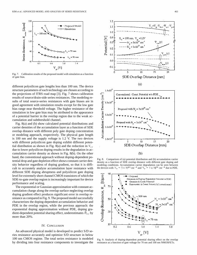
Fig. 7. Calibration results of the proposed model with simulation as a functionof gate bias.
different polysilicon gate lengths less than 100 nm. The devicestructure parameters of each technology are chosen according tothe projections of ITRS road map [3]. Fig. 7 shows calibrationresults of source/drain-side series resistances. The modeling re-sults of total source-series resistances with gate biases are ingood agreement with simulation results except for the low gatebias range near threshold voltage. The higher resistance of thesimulation in low gate bias may be attributed to the appearanceof a potential barrier in the overlap region due to the weak ac-cumulation and subthreshold channel.
Fig. 8(a) and (b) show calculated potential distributions andcarrier densities of the accumulation layer as a function of SDEoverlap distance with different poly gate doping concentrationor modeling approach, respectively. The physical gate lengthis 100 nm and the supply voltage is 1.2 V. The two deviceswith different polysilicon gate doping exhibit different poten-tial distribution as shown in Fig. 8(a) and the reduction indue to lower polysilicon doping results in the degradation in ac-cumulation carrier density as shown in Fig. 8(b). On the otherhand, the conventional approach without doping-dependent po-tential drop and gate depletion effect shows constant carrier den-sity behavior regardless of doping gradient, so that it is diffi-cult to accurately analyze accumulation layer resistance withdifferent SDE doping abruptness and polysilicon gate dopinglevel for extremely short channel CMOS transistors of which theSDE-to-gate overlap region is increasingly important for deviceperformance and scaling.
The exponential or Gaussian approximation with constant ac-cumulation charge along the overlap surface neglecting overlapdoping gradient effect produces significant error in overlap re-sistance as compared in Fig. 9. The proposed model successfullycharacterizes the doping-dependent accumulation behavior andPDE in the overlap region, while the previous approach: theexponential doping approximation without PDE, doping gra-dient-dependent potential sharing effect, underestimatesbymore than 20%.
IV. CONCLUSION
An advanced physical model is developed to predict S/D se-ries resistance accurately and optimize S/D structure in below100 nm CMOS regime. The total series resistance is modeledby dividing into four resistance components to investigate the
Fig. 8. Comparison of (a) potential distribution and (b) accumulation carrierdensity as a function of SDE overlap distance with different gate doping andmodeling conditions. Accumulation carrier degradation can be seen betweenthe devices withN = 3�10 cm andN = 1�10 cm due to PDE.
Fig. 9. Analysis of doping-dependent potential sharing effect on the overlapresistance as a function of gate voltage for 70 nm and 100 nm NMOSFETs.

464 IEEE TRANSACTIONS ON ELECTRON DEVICES, VOL. 49, NO. 3, MARCH 2002
relative contribution of each resistance component and its im-pact on CMOS scaling. The Gaussian diffusion profiles withoutfitting parameters for doping slope are assumed to minimize dis-crepancy with real profiles in SDE and deep junction region. Thespreading resistances are modeled with current spreading angleschanged by junction geometries and depletion width variations.The model considers the unique characteristics of nanometer-scale CMOSFETs comprising ultrashallow SDE junction, SDEdoping gradient effect, increased portion of potential sharingeffect in MOS structure of accumulation layer, and the crit-ical parameters associated with silicide-diffusion contact be-havior. The proposed model is verified and calibrated with sim-ulations for nanometer gate-length MOSFETs scaled accordingto ITRS roadmap and shows much accurate estimation and im-proved characterization for series resistance as compared withconventional approach. The proposed model is well suited forthe understanding of the impact of various device parameterson the source/drain series resistance and the optimization ofnanometer-scale CMOS.
APPENDIX ACALCULATION OF DEPLETION WIDTHS, , AND IN
DIFFUSEDSDE JUNCTION
To find depletion width in SDE overlap region of Fig. 4,the simplified expression of the diffusion profile describing inthe vicinity of the metallurgical junction can be used as illus-trated in Fig. 4(b) with an exponential slope as
for (25)
where is the characteristic slope of the doping profilenear the metallurgical junction. The exponential slopecan be determined from the assumption that the exponentialdoping profile in (25) has a slope identical to Gaussianprofile in (1) near the metallurgical junction, that is,
where is arbitrary point in SDE overlapregion near the metallurgical junction. Then becomes
(26)
The slope of (26) does not hold for whole SDE diffusion regionbut is meaningful only in the vicinity of the metallurgical junc-tion, since the depletion region has a limited penetration nearthe junction and the profile needs to be accurate in the limitedregion of actual depletion region. Thus the SDE/substrate junc-tion can be approximated to a one-sided exponentially gradedp-n junction in the vicinity of the metallurgical junction as il-lustrated in Fig. 4(b) and the depletion region width can befound from an iterative solution of
(27)
and
(28)
where is the depletion region on the substrate region andis the built-in voltage of p-n junction between SDE re-
gion and substrate region. Similarly, the depletion region width,in SDE region of Fig. 4 can be also found with the ap-
proximation of one-sided exponentially gradedjunction.
APPENDIX BCALCULATION OF DEPLETION WIDTH IN DIFFUSED
DEEPJUNCTION
Consider the semicircular edge of the diffused deep junctionas shown in Fig. 6. To obtain , the approximation is madeby introducing the radial Gaussian distribution of the diffusionprofile with circular coordination of which the origin is locatedin the maximum peak doping point of as illustratedin Fig. 6. In circular coordination, the doping concentrationand its junction depth become
(29)
and
(30)
where is the characteristic slope of radial deep junctionprofile given by
(31)
which is obtained from the boundary condition that.
The doping concentration in the vicinity of the metal-lurgical junction is simplified by exponential function as
for (32)
and its characteristic slope of the doping profile nearthe metallurgical junction can be found in the similar mannerwith SDE junction case. Accordingly, the depletion widthin radial direction can be found from an iterative solution of
(33)
and
(34)
where is the depletion width on the substrate region andis the built-in voltage of deep p-n junction. Then, the de-
pletion width, in diffuse deep junction can be calculated by
(35)
KIM et al.: ADVANCED MODEL AND ANALYSIS OF SERIES RESISTANCE 465
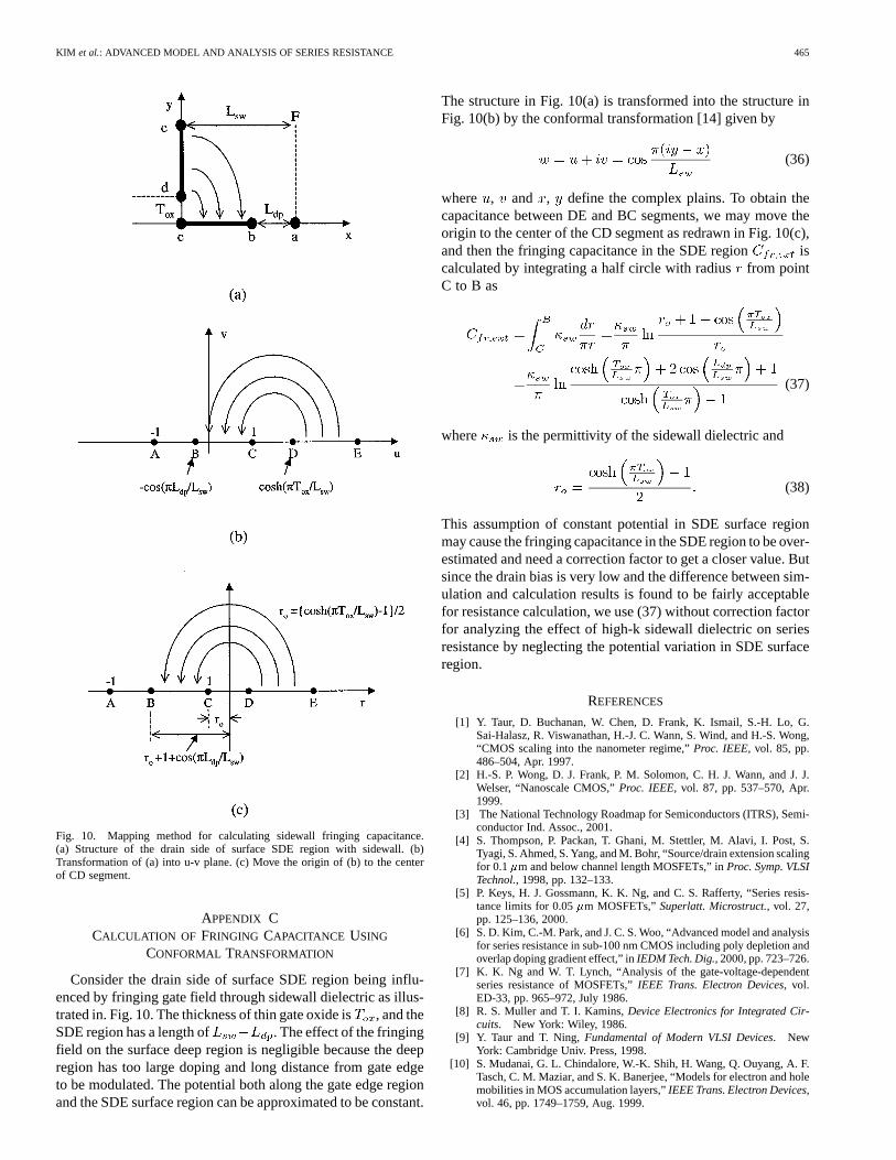
Fig. 10. Mapping method for calculating sidewall fringing capacitance.(a) Structure of the drain side of surface SDE region with sidewall. (b)Transformation of (a) into u-v plane. (c) Move the origin of (b) to the centerof CD segment.
APPENDIX CCALCULATION OF FRINGING CAPACITANCE USING
CONFORMAL TRANSFORMATION
Consider the drain side of surface SDE region being influ-enced by fringing gate field through sidewall dielectric as illus-trated in. Fig. 10. The thickness of thin gate oxide is, and theSDE region has a length of . The effect of the fringingfield on the surface deep region is negligible because the deepregion has too large doping and long distance from gate edgeto be modulated. The potential both along the gate edge regionand the SDE surface region can be approximated to be constant.
The structure in Fig. 10(a) is transformed into the structure inFig. 10(b) by the conformal transformation [14] given by
(36)
where , and , define the complex plains. To obtain thecapacitance between DE and BC segments, we may move theorigin to the center of the CD segment as redrawn in Fig. 10(c),and then the fringing capacitance in the SDE region iscalculated by integrating a half circle with radiusfrom pointC to B as
(37)
where is the permittivity of the sidewall dielectric and
(38)
This assumption of constant potential in SDE surface regionmay cause the fringing capacitance in the SDE region to be over-estimated and need a correction factor to get a closer value. Butsince the drain bias is very low and the difference between sim-ulation and calculation results is found to be fairly acceptablefor resistance calculation, we use (37) without correction factorfor analyzing the effect of high-k sidewall dielectric on seriesresistance by neglecting the potential variation in SDE surfaceregion.
REFERENCES
[1] Y. Taur, D. Buchanan, W. Chen, D. Frank, K. Ismail, S.-H. Lo, G.Sai-Halasz, R. Viswanathan, H.-J. C. Wann, S. Wind, and H.-S. Wong,“CMOS scaling into the nanometer regime,”Proc. IEEE, vol. 85, pp.486–504, Apr. 1997.
[2] H.-S. P. Wong, D. J. Frank, P. M. Solomon, C. H. J. Wann, and J. J.Welser, “Nanoscale CMOS,”Proc. IEEE, vol. 87, pp. 537–570, Apr.1999.
[3] The National Technology Roadmap for Semiconductors (ITRS), Semi-conductor Ind. Assoc., 2001.
[4] S. Thompson, P. Packan, T. Ghani, M. Stettler, M. Alavi, I. Post, S.Tyagi, S. Ahmed, S. Yang, and M. Bohr, “Source/drain extension scalingfor 0.1�m and below channel length MOSFETs,” inProc. Symp. VLSITechnol., 1998, pp. 132–133.
[5] P. Keys, H. J. Gossmann, K. K. Ng, and C. S. Rafferty, “Series resis-tance limits for 0.05�m MOSFETs,”Superlatt. Microstruct., vol. 27,pp. 125–136, 2000.
[6] S. D. Kim, C.-M. Park, and J. C. S. Woo, “Advanced model and analysisfor series resistance in sub-100 nm CMOS including poly depletion andoverlap doping gradient effect,” inIEDM Tech. Dig., 2000, pp. 723–726.
[7] K. K. Ng and W. T. Lynch, “Analysis of the gate-voltage-dependentseries resistance of MOSFETs,”IEEE Trans. Electron Devices, vol.ED-33, pp. 965–972, July 1986.
[8] R. S. Muller and T. I. Kamins,Device Electronics for Integrated Cir-cuits. New York: Wiley, 1986.
[9] Y. Taur and T. Ning,Fundamental of Modern VLSI Devices. NewYork: Cambridge Univ. Press, 1998.
[10] S. Mudanai, G. L. Chindalore, W.-K. Shih, H. Wang, Q. Ouyang, A. F.Tasch, C. M. Maziar, and S. K. Banerjee, “Models for electron and holemobilities in MOS accumulation layers,”IEEE Trans. Electron Devices,vol. 46, pp. 1749–1759, Aug. 1999.
466 IEEE TRANSACTIONS ON ELECTRON DEVICES, VOL. 49, NO. 3, MARCH 2002
[11] K. Chen, H. C. Wann, P. K. Ko, and C. Hu, “The impact of device scalingand power supply change on CMOS gate performance,”IEEE ElectronDevices Lett., vol. 17, pp. 202–204, May 1996.
[12] K. F. Schuegraf, C. C. King, and C. Hu, “Impact of polysilicon depletionin thin oxide MOS technology,” inProc. Symp. VLSI Technol., 1993, pp.86–90.
[13] D. L. Kencke, W. Chen, H. Wang, S. Mudanai, Q. Ouyang, A. Tasch, andS. K. Banerjee, “Source-side barrier effects with very high-K dielectricsin 50 nm Si MOSFETs,” in57th Annu. DRC Dig., 1999, pp. 22–23.
[14] S. S. Chung and T. Li, “An analytical threshold-voltage model oftrench-isolated MOS devices with nonuniformly doped substrates,”IEEE Trans. Electron Devices, vol. 39, pp. 614–622, Mar. 1992.
[15] K. Varaharamyan and E. J. Verret, “A model for specific contact resis-tance application for Titanium silicide-silicon contact,”Solid-State Elec-tron., vol. 39, pp. 1601–1607, Nov. 1996.
[16] D. B. Scott, R. A. Chapman, C. Wei, S. S. Mahant-Shetti, R. A. Haken,and T. C. Holloway, “Titanium disilicide contact resisitivity and its im-pact on 1-�m CMOS circuit performance,”IEEE Trans. Electron De-vices, vol. ED-34, pp. 562–574, Mar. 1987.
[17] Y.-S. Chieh, A. H. Perera, and J. P. Krusius, “Series resistance of sili-cided ohmic contacts for nanoelecronics,”IEEE Trans. Electron De-vices, vol. 39, pp. 1882–1888, Aug. 1992.
[18] B.-Y. Tsui and M.-C. Chen, “Series resistance of self-aligned silicidedsource/drain structure,”IEEE Trans. Electron Devices, vol. 40, pp.197–206, Jan. 1993.
Seong-Dong Kim(S’94–M’97) was born in Chonan, Korea, in 1967. He re-ceived the B.S., M.S., and Ph.D. in electrical engineering from Seoul NationalUniversity, Seoul, Korea, in 1990, 1992, and 1996, respectively. His graduateresearch was focused on the power semiconductor devices and ICs.
From 1996 to 1999, he was with the System IC Research and DevelopmentCenter, Hyundai Electronics Industries, Seoul, Korea, where he engaged in theresearch and development of submicron CMOS technologies, CMOS imagesensors, and high voltage CMOS-DMOS ICs. In December 1999, he joined theDepartment of Electrical Engineering, University of California, Los Angeles,as a Research Engineer, where he has been conducting research on the physics,technology, and modeling of nanometer-scale CMOS devices. His research in-terests include the design, fabrication, and modeling of CMOS VLSI technolo-gies, SOI devices, and power semiconductor devices.
Cheol-Min Park (S’96–M’01) was born in Seoul, Korea, in 1971. He receivedthe B.S. and M.S. degrees in electrical engineering from Seoul National Univer-sity, Seoul, in 1994 and 1996, respectively, where he is currently pursuing thePh.D. degree in the School of Electrical and Computer Engineering.
His current research interests are in electrical and structural properties ofpoly-Si thin-film transistors.
Jason C. S. Woo(S’83–M’87–SM’97) received the B.A.Sc. (Hons.) degree inengineering science from the University of Toronto, Toronto, ON, Canada, in1981, and the M.S. and Ph.D. degrees in electrical engineering from StanfordUniversity, Stanford, CA, in 1982 and 1987, respectively.
In 1987, he joined the Department of Electrical Engineering, the University ofCalifornia, Los Angeles, where he is currently a Professor. His research interestsare in the physics and technology of novel device and device modeling, andhe has authored more than 100 papers in technical journals and the refereedconference proceedings in these areas.
Dr. Woo served on the IEEE IEDM Program Committee from 1989 to 1990and from 1994 to 1996, and was Publicity Vice Chairman in 1992 and the Pub-licity Chairman in 1993. He has been the Workshop Chairman and a TechnicalCommittee Member of the VLSI Technology Symposium since 1992. He hasserved on the committee for the IEEE SOI Conference since 1995. He receiveda Faculty Development Award from IBM from 1987 to 1989.


![P087 Reliability Modeling on 90 nm n-channel MOSFETs with ...€¦ · [6] E. Maricau and G. Gielen,Analog IC Reliability in Nanometer CMOS,Springer Science Business Media New](https://img.pdfslide.us/doc/110x75/5fb67b16ce590245f2046e91/p087-reliability-modeling-on-90-nm-n-channel-mosfets-with-6-e-maricau-and.jpg)