Embed Size (px)
Citation preview

Advanced Magnetoresistive Sensors for IndustrialApplications
Tiago Afonso Carocho de Sousa Costa
Thesis to obtain the Master of Science Degree in
Engineering Physics
Supervisor: Prof. Susana Isabel Pinheiro Cardoso de Freitas
Examination Committee
Chairperson: Prof. Pedro Miguel Félix BrogueiraSupervisor: Prof. Susana Isabel Pinheiro Cardoso de FreitasMember of the Committee: Dr. Karla Marina Jaimes Merazzo
October 2017

ii

Acknowledgments
First of all I would like to thank Prof. Susana Freitas for the opportunity to work in INESC-MN for the last
year and for all the guidance and support, for also allowing me to develop as a researcher, a professional
and a person.
I would like to especially thank Karla for her unconditional support and help in this project. Without
her, the challenges would have been much harder to overcome. I would also like to acknowledge all
the senior researchers and PhDs for always being available for any questions or doubts, and also the
technical staff for teaching me the processes and for their availability.
I’m very grateful to all my friends and colleagues at INESC-MN for the great team-work environment,
and thank you for the lunch hours where my mind could relax for a while.
Thank you to all my friends at Tecnico for making the last five years not only about studying and
working and for providing some of the best moments in my life. To my big friends Marisa and Ana for
keeping me sane throughout the years. I’m especially thankful to Basti for supporting me emotionally,
especially during the last few months.
Last but not least, I acknowledge my family: my father Pedro, my mother Gui and my brother Diogo
and sister Marta for always being present no matter what, and for supporting me unconditionally. Thank
you for everything!
iii

iv

Resumo
Metrologia e posicionamento preciso sao de extrema importancia para a industria. Hoje em dia, ex-
iste uma procura competitiva para aparelhos diminutos, de menor custo e capazes de cumprir mesmo
em ambientes adversos. A codificacao precisa pode, por isso, beneficiar de tecnologia magnetica.
Sensores magnetoresistivos (MR) sao de tamanho diminuto, de baixo custo e oferecem grande sen-
sibilidade. Como portador de informacao, o uso de tinta magnetica (TM) e vantajosa em relacao a
tecnologia magnetica existente.
Sensores MR avancados - as juncoes de efeito de tunel - sao implementadas num sistema, em
conjugacao com ımanes permanentes, com o objetivo de magnetizar e ler padroes de TM. O de-
senvolvimento deste sistema e feito em dois passos essenciais. Primeiro a determinacao da melhor
configuracao ıman-sensor atraves de medicoes e de simulacao por modulacao de elementos finitos.
Posteriormente e feita a validacao de duas configuracoes de sensores diferentes. Validacao feita
medindo estruturas bem definidas, microfabricadas em ambiente de sala limpa, de uma liga ferro-
magnetica, e posteriror simulacao 2D das mesmas, usando a aproximacao de Coulomb para o calculo
do campo magnetico.
De seis configuracoes de ıman-sensor diferentes, duas foram escolhidas e testadas. A configuracao
resultante e capaz tanto de eficientemente magnetizar as estruturas de TM, como de nao influenciar a
resposta magnetica dos sensores. A simulacao das estruturas ferromagneticas permitiu a validacao das
duas configuracoes de sensores consideradas, resultando na escolha do sensor com maior resolucao
espacial e sensibilidade alta, providenciando assim uma base para um futuro desenvolvimento e optimizacao
do sistema.
Palavras-chave: Juncoes de efeito de tunel, Tinta magnetica, Codificadores magneticos,
Medicoes de campo magnetico disperso, Simulacao de campo magnetico
v

vi

Abstract
In Industry, metrology and accurate positioning is of major relevance. Nowadays there is competitive
demand for small size devices at lowest cost possible and capable of performing even in harsh environ-
ments. Precision encoding can therefore benefit from magnetic technology. As a reading technology,
magnetoresistance (MR) devices offer low sizes, high sensitivity and low costs. For information storage,
patterns of magnetic ink (MI) as an alternative to the existing technology is also of advantage.
Advanced MR sensors - the magnetic tunnel junctions - are therefore implemented in a system along-
side magnets aimed to magnetize and read MI patterns. The development of this system is done in two
main stages. First the search for the best magnet-sensor configuration using both simulation with finite
element modeling (FEM) and measurements. Then the validation of different sensor array configura-
tions. This validation is done through measurements of well-defined structures of a hard ferromagnetic
alloy, micro-fabricated in a clean-room environment, and comparison with a 2D simulation, which is
based on a Coulomb approach to the calculation of the magnetic field.
From six different magnet configurations, two were chosen and tested. The resulting configuration is
able to efficiently magnetized the MI structures as well as not influence the sensor’s magnetic response.
The simulation with the hard magnetic micro-fabricated structures allowed for the validation of both
sensor configurations considered in this work - resulting in the choice of a high spatial resolution and
high sensitivity sensor, providing a basis for further system development and optimization.
Keywords: Magnetic tunnel junctions, Magnetic ink, Magnetic encoder, Stray field measure-
ment, Magnetic field simulation
vii

viii

Contents
Acknowledgments . . . . . . . . . . . . . . . . . . . . . . . . . . . . . . . . . . . . . . . . . . . iii
Resumo . . . . . . . . . . . . . . . . . . . . . . . . . . . . . . . . . . . . . . . . . . . . . . . . . v
Abstract . . . . . . . . . . . . . . . . . . . . . . . . . . . . . . . . . . . . . . . . . . . . . . . . . vii
List of Tables . . . . . . . . . . . . . . . . . . . . . . . . . . . . . . . . . . . . . . . . . . . . . . xi
List of Figures . . . . . . . . . . . . . . . . . . . . . . . . . . . . . . . . . . . . . . . . . . . . . xiii
Nomenclature . . . . . . . . . . . . . . . . . . . . . . . . . . . . . . . . . . . . . . . . . . . . . . xv
1 Introduction 1
1.1 Motivation . . . . . . . . . . . . . . . . . . . . . . . . . . . . . . . . . . . . . . . . . . . . . 1
1.2 State of the Art . . . . . . . . . . . . . . . . . . . . . . . . . . . . . . . . . . . . . . . . . . 1
1.2.1 Positioning Systems - Encoders . . . . . . . . . . . . . . . . . . . . . . . . . . . . 1
1.2.2 Magnetic Sensors for Scanning Applications . . . . . . . . . . . . . . . . . . . . . 2
1.2.3 Magnetoresistive Sensors . . . . . . . . . . . . . . . . . . . . . . . . . . . . . . . . 3
1.2.4 Magnetic Ink . . . . . . . . . . . . . . . . . . . . . . . . . . . . . . . . . . . . . . . 4
1.3 Objectives . . . . . . . . . . . . . . . . . . . . . . . . . . . . . . . . . . . . . . . . . . . . . 5
2 Theoretical Background 7
2.1 Magnetism and Magnetic Materials . . . . . . . . . . . . . . . . . . . . . . . . . . . . . . . 7
2.1.1 Magnetic Dipole Moment . . . . . . . . . . . . . . . . . . . . . . . . . . . . . . . . 7
2.1.2 Topics of Magnetostatics . . . . . . . . . . . . . . . . . . . . . . . . . . . . . . . . 8
2.1.3 Classification of Magnetic Materials . . . . . . . . . . . . . . . . . . . . . . . . . . 11
2.1.4 Magnetic Ink . . . . . . . . . . . . . . . . . . . . . . . . . . . . . . . . . . . . . . . 13
2.2 Magnetic Tunnel Junctions . . . . . . . . . . . . . . . . . . . . . . . . . . . . . . . . . . . . 14
2.2.1 Tunnel Magnetoresistance . . . . . . . . . . . . . . . . . . . . . . . . . . . . . . . . 14
2.2.2 Structure . . . . . . . . . . . . . . . . . . . . . . . . . . . . . . . . . . . . . . . . . 15
2.2.3 MTJ Linearization . . . . . . . . . . . . . . . . . . . . . . . . . . . . . . . . . . . . 16
2.2.4 Sensitivity, Voltage Bias and the Output Signal . . . . . . . . . . . . . . . . . . . . 18
3 System Description and Characterization 21
3.1 System Description . . . . . . . . . . . . . . . . . . . . . . . . . . . . . . . . . . . . . . . . 21
3.1.1 Magnetic Ink . . . . . . . . . . . . . . . . . . . . . . . . . . . . . . . . . . . . . . . 21
3.1.2 Configurations . . . . . . . . . . . . . . . . . . . . . . . . . . . . . . . . . . . . . . 22
ix

3.1.3 Simulation of the Magnets Configurations . . . . . . . . . . . . . . . . . . . . . . . 24
3.2 Sensing Head Characterization . . . . . . . . . . . . . . . . . . . . . . . . . . . . . . . . . 30
3.2.1 Magnetoresistive Sensors . . . . . . . . . . . . . . . . . . . . . . . . . . . . . . . . 30
3.2.2 Magneto-transport Characterization Tool . . . . . . . . . . . . . . . . . . . . . . . . 30
3.2.3 Magnetotrasport Characterization . . . . . . . . . . . . . . . . . . . . . . . . . . . 31
4 Hard Magnetic CoCrPt Structures 37
4.1 Micro-Fabrication . . . . . . . . . . . . . . . . . . . . . . . . . . . . . . . . . . . . . . . . . 37
4.1.1 Deposition by Magnetron Sputtering . . . . . . . . . . . . . . . . . . . . . . . . . . 38
4.1.2 Pole Definition by Litography . . . . . . . . . . . . . . . . . . . . . . . . . . . . . . 39
4.1.3 Etching by Ion-Milling . . . . . . . . . . . . . . . . . . . . . . . . . . . . . . . . . . 40
4.1.4 Magnetization Definition . . . . . . . . . . . . . . . . . . . . . . . . . . . . . . . . . 41
4.1.5 Magnetic Properties Measurement - Vibrating Sample Magnetometer . . . . . . . 41
4.2 Simulation Model of the CoCrPt Structures . . . . . . . . . . . . . . . . . . . . . . . . . . 42
4.2.1 Magnetic Field from a Flat Surface - 2D Model . . . . . . . . . . . . . . . . . . . . 43
4.2.2 Two-Dimensional Field from the CoCrPt Sample . . . . . . . . . . . . . . . . . . . 44
5 Measurements 47
5.1 Measurement System . . . . . . . . . . . . . . . . . . . . . . . . . . . . . . . . . . . . . . 47
5.2 Measurements on Magnetic Ink Samples . . . . . . . . . . . . . . . . . . . . . . . . . . . 49
5.3 Sensor Validation with CoCrPt Samples . . . . . . . . . . . . . . . . . . . . . . . . . . . . 49
5.3.1 Sensor S1 . . . . . . . . . . . . . . . . . . . . . . . . . . . . . . . . . . . . . . . . . 50
5.3.2 Sensor S2 . . . . . . . . . . . . . . . . . . . . . . . . . . . . . . . . . . . . . . . . . 52
6 Conclusions 55
Bibliography 57
A CoCrPt Structures Micro-Fabrication Process Runsheet A.1
x

List of Tables
3.1 Physical parameters of the magnets used. . . . . . . . . . . . . . . . . . . . . . . . . . . . 24
3.2 Physical parameters derived from the transfer curves of sensor S1, without magnets and
with configuration Std 1. . . . . . . . . . . . . . . . . . . . . . . . . . . . . . . . . . . . . . 33
3.3 Physical parameters derived from the transfer curves of sensors S1 and S2, without mag-
nets and with configuration Std 3 and a = 0.5 mm. . . . . . . . . . . . . . . . . . . . . . . 35
4.1 Parameters for sputter deposition of CoCrPt. . . . . . . . . . . . . . . . . . . . . . . . . . 38
4.2 Parameters for etching of CoCrPt. . . . . . . . . . . . . . . . . . . . . . . . . . . . . . . . 41
xi

xii

List of Figures
1.1 A scheme of a magnetic rotary encoder. . . . . . . . . . . . . . . . . . . . . . . . . . . . . 2
1.2 Details of the different Magnetoresistive sensor technologies. . . . . . . . . . . . . . . . . 4
1.3 Applications of magnetic ink. . . . . . . . . . . . . . . . . . . . . . . . . . . . . . . . . . . 4
2.1 Calculation of the magnetic field outside a magnetized cylinder. . . . . . . . . . . . . . . . 10
2.2 Magnetic response of a diamagnetic and paramagnetic material in the presence of an
external magnetic field. . . . . . . . . . . . . . . . . . . . . . . . . . . . . . . . . . . . . . 11
2.3 Magnetic response of a ferromagnetic material in the presence of an external magnetic
field. . . . . . . . . . . . . . . . . . . . . . . . . . . . . . . . . . . . . . . . . . . . . . . . . 12
2.4 Magnetic response of a superparamagnetic material in the presence of an external mag-
netic field. . . . . . . . . . . . . . . . . . . . . . . . . . . . . . . . . . . . . . . . . . . . . . 13
2.5 Schematic of the spin-dependent tunneling effect. . . . . . . . . . . . . . . . . . . . . . . 14
2.6 Basic structure of a MTJ sensor. . . . . . . . . . . . . . . . . . . . . . . . . . . . . . . . . 15
2.7 Ideal transfer curve of a MTJ sensor. . . . . . . . . . . . . . . . . . . . . . . . . . . . . . . 17
2.8 Typical structure of a junction with both sensing and reference layer pinned. . . . . . . . . 18
3.1 Configuration standards considered for the project. . . . . . . . . . . . . . . . . . . . . . . 23
3.2 Proposed concept for the system. . . . . . . . . . . . . . . . . . . . . . . . . . . . . . . . . 24
3.3 3D geometry used on the simulation software. Geometry of the magnets: 10×4×1 mm3;
b = 6 mm. . . . . . . . . . . . . . . . . . . . . . . . . . . . . . . . . . . . . . . . . . . . . . 25
3.4 Magnetic field vectors for the configuration with magnets with OOP magnetization . . . . 26
3.5 Simulation of the different components of the field in given regions of the simulated space
with Std 1. . . . . . . . . . . . . . . . . . . . . . . . . . . . . . . . . . . . . . . . . . . . . . 27
3.6 Magnetic field vectors for the configuration with magnets with OOP magnetization . . . . 28
3.7 Simulation of the different components of the field in given regions of the simulated space
with IP magnetization magnets. . . . . . . . . . . . . . . . . . . . . . . . . . . . . . . . . . 29
3.8 Plot of Bx, By and Bz on line 4. Sensor at a = 0.5 mm. . . . . . . . . . . . . . . . . . . . 29
3.9 MTJ pillar structure and scheme of the junction array of sensors S1 and S2. . . . . . . . . 31
3.10 Reference transfer curves of sensors S1 and S2, without magnets present on the system. 32
3.11 Set of transfer curves obtained for sensor S1 in a Std 1 configuration, alongside the ref-
erence curve. . . . . . . . . . . . . . . . . . . . . . . . . . . . . . . . . . . . . . . . . . . . 33
xiii

3.12 Study on the transfer curves of sensor 1, with configuration standard Std 3. . . . . . . . . 34
3.13 Transfer curves for the sensor S1 and S2, with configuration Std 3 and a = 0.5 mm. . . . 35
4.1 Structure of the micro-fabricated CoCrPt structures. . . . . . . . . . . . . . . . . . . . . . 37
4.2 Schematic view of the deposition chamber of Alcatel SMC450. . . . . . . . . . . . . . . . 39
4.3 Hysteresis loop of magnetization vs. applied field for the deposited magnetic alloy CoCrPt. 42
4.4 Scheme of the simulation geometry for the CoCrPt structures. . . . . . . . . . . . . . . . . 42
4.5 Ilustration of the derivaton of the magnetic field from a 2D line of constant charge. . . . . 43
4.6 Scheme of the contributions to the calculation of the field of just two PM CoCrPt structures. 45
5.1 The 2D scanning setup used to measure the stray fields from the magnetic ink and CoCrPt
samples. . . . . . . . . . . . . . . . . . . . . . . . . . . . . . . . . . . . . . . . . . . . . . 48
5.2 A scheme of the scanning measurements done on the different CoCrPt samples. . . . . . 48
5.3 Simulation done for the CoCrPt sample with PP=1mm and at a RD=500±14µm, with N=8. 50
5.4 Comparison of the simulations and measurements done on CoCrPt samples with different
Pole-Pitches, using sensor S1. . . . . . . . . . . . . . . . . . . . . . . . . . . . . . . . . . 51
5.5 Average amplitudes measured both in the measurements and simulations for sensor S1
for each sample at a RD of half the PP. . . . . . . . . . . . . . . . . . . . . . . . . . . . . . 52
5.6 Comparison of the simulations and measurements done on CoCrPt samples with different
Pole-Pitches, using sensor S2. . . . . . . . . . . . . . . . . . . . . . . . . . . . . . . . . . 53
5.7 Amplitudes measured both in the measurements and simulations for sensor S2 for each
sample at a RD of half the PP. . . . . . . . . . . . . . . . . . . . . . . . . . . . . . . . . . . 54
xiv

Nomenclature
AFM Anti-ferromagnetic
AMR Anisotropic Magnetoresistance
CPP Current Perpendicular to the Plane
FM Ferromagnetic
GMI Giant Magneto Impedance
GMR Giant Magnetoresistance
IP In-Plane
LIH Linear, Isotropic and Homogeneous
MI Magnetic Ink
MICR Magnetic Ink Character Recognition
MR Magnetoresistance
MTJ Magnetic Tunnel Junction
NM Nonmagnetic
OOP Out-Of-Plane
PM Permanent Magnet
PP Pole-Pitch
PR Photo-Resist
RD Reading Distance
SAF Synthetic Anti-ferromagnetic
SNR Signal-to-Noise-Ratio
SQUID Scanning Superconducting Quantum Interference Device
SyF Synthetic Ferrimagnetic
TMR Tunnel Magnetoresistance
xv

xvi

Chapter 1
Introduction
1.1 Motivation
Metrology and accurate positioning is of major relevance for industry. Nowadays there is competitive
demand for small size devices with the lowest cost possible and capable of performing even in harsh
environments. Currently, the most widespread used technology is optical detection, which allow high
accuracy, resolution and reliability. However, in harsh environments such systems become bigger, more
expensive and more fragile. Precision encoding can therefore benefit from the use of magnetic technol-
ogy and in particular from magnetoresistance (MR), which offers clear advantages when compared to
optical detection. MR sensors - in particular state of the art Magnetic Tunnel Junctions (MTJs) - can be
produced in micrometic dimensions at massive scale, at low cost and capable of high sensitivity to weak
magnetic fields [1, 2]. Encoder systems can also take advantage on new, low cost magnetic encoding
tracks. The use of Magnetic Ink (MI), already present in many security applications, allows for the low
cost replacement of the existing technology [3, 4].
1.2 State of the Art
1.2.1 Positioning Systems - Encoders
Encoders are devices capable of converting mechanical rotational or linear movement into an analog or
digital signal. The typical encoder has just two components: a reading head and a track, which encodes
the information. Both components depend on the technology used.
Current industrial applications rely on encoders to determine positions, angles, rotational speeds,
and other related variables. Currently the most widespread measuring principle on encoders is optical
[5]. This method is the first choice due to its high accuracy, resolution and reliability. However, sensors for
detecting such variables need to have a stable operation in harsh environments as well as provide high
resolution and high accuracy. Generally, optical encoders can have high resolution but may not be ideal
for some typical industrial environments such as those with oil, dirt, dust or fluctuating temperature.
1

When prepared for such environments through protection with encasement or other methods, optical
encoders tend to not meet the reduced prices or small sizes that are in increasing demand for industrial
applications [5]. Magnetic technology can overcome these problems and replace optical encoders in
many applications.
When compared to optical encoders, magnetic technology based encoders can take the form of very
small, inexpensive devices, in high volume applications, such as industrial automation systems, anti-
block braking systems or medical equipment [6]. Magnetic encoders, like any encoder, have a reading
head using some sort of magnetic sensor technology, and a magnetic encoding track comprised of a
magnetic media with a given magnetic pattern, which encodes the position. It is the magnetic sensor on
the reading head that by measuring the stray magnetic field produced between the poles in the magnetic
media that positioning information can be extracted [4].
Figure 1.1: A scheme of a magnetic rotary encoder. The track is represented with red and green bitsrepresenting the magnetic poles. Taken from [4].
The company Bogen Electronic GmbH produces and commercializes magnetic encoders [4]. This
company utilizes mainly reading-heads with Hall-effect based sensors and is already implementing MR
based sensors, placing itself in the front of the development of MR based measuring tools. The tracks
produced by this company are state-of-the-art hard magnetic, which are made of a continuous magnetic
media: an elastomer filled with ferrite. The magnetic poles are then engraved in the track using a process
patented by this company. On Figure 1.1, a scheme of a rotary magnetic encoder is presented. The
magnetic track is located around the axis and in this case, the position is encoded as a periodically
alternating north and south pole.
1.2.2 Magnetic Sensors for Scanning Applications
Some sensing technologies have been used for magnetic scanning of a surface, such as Hall-Effect,
SQUID (Scanning Superconducting Quantum Interference Device) and GMI (Giant Magneto Impedance)
[7]. For scanning applications two very important properties of the sensors are evaluated: the Spatial
Resolution, which is normally related to the size of the sensor and it’s the minimum size that the sensor
2

can measure (the smallest structure it can measure); and also the Field Detection or Sensitivity of the
sensor, which determines the lowest magnetic field and field variation it can measure.
Due to its high field detection and somewhat smaller sizes, SQUIDs are mainly used for NDT testing
such as buried defects, however, since it operates at cryogenic temperatures, they are not suitable for
most industrial applications.
GMI sensors have very high magnetic field sensitivity of as high as 500 %/Oe, but have very low
spatial resolution due to its required large dimensions, being mainly used for NDT such as surface
cracks detection.
Hall-Effect sensors are transducers, on which a change of the external magnetic field translates into
a change in the output voltage of the sensor [8]. Although these sensors offer lower field detection than
other magnetic sensing technologies [9], they have the advantage of reaching lower spatial resolution
(in the nanometer scale).
For positioning applications, the most widely used magnetic sensor is the based on Hall-Effect sen-
sor. It has thus far allowed for good magnetic field sensitivity and also good spatial resolution and
adaptable for industrial environment. However, industry is demanding for even higher resolution and
better performance. That’s why MR based sensor are being developed and implemented on positioning
devices for industrial applications [6, 4].
1.2.3 Magnetoresistive Sensors
The use of magnetic sensors for scanning applications is not new and already widely spread in today’s
technology, such as in Non-Destructive Testing (NDT) using eddy current inspection, document valida-
tion with magnetic ink, hard disk drives and even biological applications [1, 7, 10].
The MR sensor is a solid state transducer, which converts directly a magnetic field into a resistance.
Magnetoresistance is defined as the change in the electrical resistance of a material as a response to an
externally applied magnetic field. The idea of using MR sensors as elements to detect magnetic stray
fields arises from the widely implemented hard-disk-heads [7]. The spatial resolution of a MR device
depends directly on the dimension of the sensors used. Unlike the other previously discussed magnetic
technologies, MR sensors are easily scalable using micro- and nanofabrication techniques, which allows
the implementation of very small devices with very low spatial resolution [1, 2].
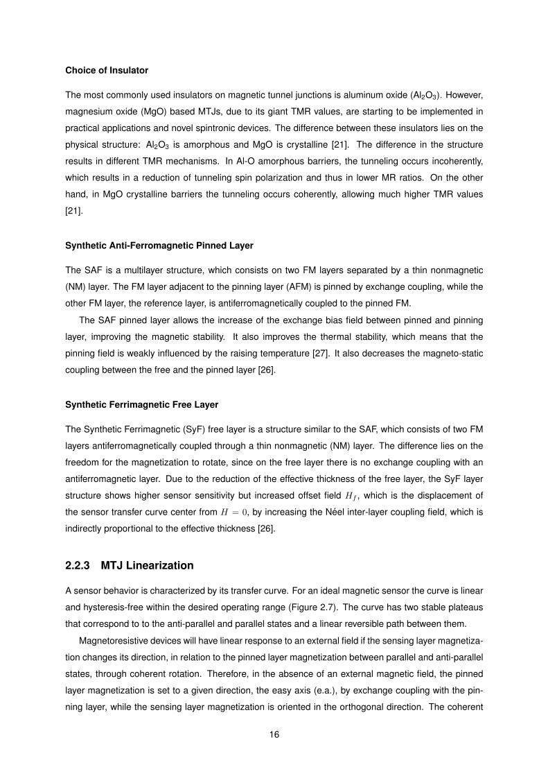
Depending on the physical principle, the MR sensors can be divided into three different types: the
Anisotropic Magnetoresistance (AMR), the Giant Magnetoresistance (GMR) and the Tunnel Magnetore-
sistance (TMR). The table on Figure 1.2 resumes the main characteristics and differences between the
three kinds of devices.
When compared to Hall-Effect sensors, AMR sensor have higher sensitivities and comparable spatial
resolutions. However, nowadays due to the clear advantages regarding field detection, GMR and TMR
sensors prove much more advantageous for magnetic sensing than AMR sensors, thus replacing AMR
in most applications.
MR devices and in specificic state-of-the-art Magnetic Tunnel Junctions (MTJs) have high Magne-
3

Figure 1.2: Details of the different Magnetoresistive sensor technologies. Taken from [2].
toresistance ratios (on the order of 300% [2]) which lead to high sensitivity and thus low field detection.
They can also be fabricated in large scale and at low costs, being also very easily implemented. They
are therefore a very good solution for positioning measurements, and has the sensing technology for
magnetic encoders.
1.2.4 Magnetic Ink
For magnetic measuring purposes, magnetic ink (MI) can be very versatile. As a liquid, this ink is com-
monly composed of four types of ingredients: the colorants or magnetic pigments, where the magnetic
behavior is introduced and have sizes mostly of nanometer scale (70 nm for Fe3O4 nanoparticles [11]);
the vehicles or binders, which disperse and bind the pigments modifying the rheological and mechanical
properties; the solvents which dissolve the other components and adjusts its viscosity; and additives
which depend on the properties to be enhanced [12].
(a) A typical bank check with a MICR security line on thebottom part, taken from [13].
(b) The magnetic ink profile of the serial number of a 20Cbank note, taken from [14]
Figure 1.3: Applications of magnetic ink.
Traditionally magnetic ink is used as one of the most important counterfeit materials. It has been
4

drawing wide attention and applied to vital fields for checking authenticity, such as for identity cards,
checks, paper currency, tickets, and others, which is do to their efficient information storage, legibility,
efficient anti-counterfeit and low cost [3]. The main use of magnetic ink is, however, on MICR (Magnetic
Ink Character Recognition), which is used on checks to add an extra layer of security to these documents
[13]. Another wide use passes by impregnating this ink on banknotes, such as in the 20C bill, which
provide a forgery control test using an appropriate magnetic reading head [14]. These two applications
are exemplified on Figure 1.3.
1.3 Objectives
This work is developed in the scope of the project GePos. It is a collaborative project between INESC-
MN and Bogen Electronic GmbH. This project has the main objective of developing a positioning system
based on encoding using magnetic ink, read by state-of-the-art TMR sensors. Thus developing a com-
petitive positioning solution, which is lower in cost production and as reliable as the existing technologies.
The work developed for this master’s thesis makes the first approach and takes the first steps on
the development of such a system. As the main goal comes the development of a reading head based
on state-of-the-art TMR sensors for a magnetic encoder, on which the information is produced using
magnetic ink.
5

6

Chapter 2
Theoretical Background
2.1 Magnetism and Magnetic Materials
2.1.1 Magnetic Dipole Moment
In solid state magnetism, the elementary quantity is the magnetic moment m [15]. In the atomic level, the
magnetic moment arises from two main sources: the orbital movement of electrons around the nucleus,
and the electron spin. Except for some transition metal atoms or ions, which retain a resultant moment
on the atomic scale of the solids, most of the atomic magnetic moments tend to cancel out. Of course,
in a paramagnetic state of a solid, the moments cancel out - but due to thermal fluctuations. They arise
spontaneously in a ferromagnetic ordered state.
Fundamental in magnetostactics is the continuous media approximation , on which the magnetization
of a solid is represented by the quantity M. This quantity is no more than a time averaged local magnetic
moment density, or, given a mesoscopic volume δV :
δm = MδV. (2.1)
In a ferromagnetic domain it is the spontaneous magnetization MS, or in the case of a paramagnet or
diamagnet induced by an applied field, the arose uniform magnetization.
The magnetization can also usually be extended to a macroscopic average over a sample as a sum
of all domains i, with volume Vi:
M =∑i MiVi∑i Vi
. (2.2)
According to Ampere, a magnet is equivalent to a circulating electric current, and therefore, the
elementary magnetic moment can be represented by a tiny current loop, which is generally calculated
with:
m = 12
∫r× j (r) d3r, (2.3)
7

where j (r) is the current density at point r.
The units of the magnetic moment are Am2 and of the magnetization A/m (as defined in equation
2.1).
2.1.2 Topics of Magnetostatics
The B-field
The field created by the magnetic moment has the same form of an electric dipole p = qδl formed of
positive and negative charges ±q separated by a distance δl, being the vector p directed from −q to +q.
Hence regarding the magnetic moment as a magnetic dipole [15].
The magnetic field δB created by a small current element jδV at any point is given by the Biot-Savart
law:
δB = −µ0
4πr× jr3 δV, (2.4)
where µ0 is the magnetic permeability in free space. With integration of this equation arises the magnetic
moment m, and in terms of the position vector r:
B = µ0
4π
[3(m · r)r
r5 − mr3
]. (2.5)
The field falls off as the cube of the distance from the magnet. The field thus defined has certain
properties, which are related to the Maxwell’s equations. First it is divergenceless:
∇ ·B = 0, (2.6)
which means it has no sources or sinks. This field is said to be solenoidal - the lines of force form
continuous loops. It is also called the magnetic flux density, since from Gauss’s theorem the element
magnetic flux dΦ = B · dA can be defined, being dA the area through which the magnetic flux flows.
The B-field can be created by a) moving charges, including electric current; and b) magnetic moments,
which are equivalent to current loops. In a steady state, the relation between the magnetic flux density
B and the current density j is given by the Maxwell’s equation:
∇×B = µ0j. (2.7)
This relation is specially used when deriving Ampere’s law and calculating field due to highly symmetric
current distributions. The B-field has units the Tesla (T).
The H-field
The magnetic H-field is an indispensible auxiliary field when dealing with magnetic materials. The
magnetization of a solid reflects the local value of H. In free space, both the B and H are related
by the magnetic permeability µ0 as B = µ0H. Therefore, in free space, the derivation of both fields
8

is interchangeable and immediate. The difference arises in a material medium, where equation 2.7 is
related, instead, to the total current density [15, 16]:
∇×B = µ0 (jc + jm) , (2.8)
where jc and jm are respectively the conduction current (such as in electrical circuits) and the magne-
tization current (associated with the magnetized medium). As opposed to jc, jm cannot be measured.
However it is related to the magnetization through the relation jm = ∇×M.
So that the relation from equation 2.7 holds for these materials, with quantifiable physical parameters,
a new auxiliary field (the H-field) is defined such that ∇ ×H = jc. This field relates to the B-field and
the magnetization M through the relation:
H = Bµ0−M. (2.9)
This field is, however, no longer divergenceless. It has sources and sinks associated with nonuniformity
of the magnetization:
∇ ·H = −∇ ·M. (2.10)
This definition, when one compares to the electric field, implies the existence of fictitious charges, usually
called North and South Poles. The field of H appear to originate on these horizontal surfaces of the
magnet, where a magnetic charge density σm = M · en exists, being en the unit vector normal to the
surface. So we can imagine that H, like the electric field, is created by a distribution of positive and
negative magnetic charges qm, which would be given by the relation:
H = qm4π
rr3 . (2.11)
The magnitude of the field falling with the square of the distance. This is called the Coulombian approach
to the magnetic field.
H is not only created by conduction currents. Any magnet will produce this field both in space and
in its own volume. Therefore H can also be written as the sum of the contributions from the conduction
currents Hc and the magnetization distributions Hm:
H = Hc + Hm. (2.12)
The second contribution is known as the stray field when outside a magnet or as the demagnetizing field
(Hd) within it, since therein it is oppositely directed to M. The units of H are A/m, the same as for M.
Magnetic susceptibility and permeability
For some materials, the B-field and the H-field can be further related to each other using the perme-
ability [15]. The simplest materials are linear, isotropic and homogeneous (LIH). This means that the
9

susceptibility (χ) is small, and a small uniform magnetization is induced in the same direction as an
external field. The magnetization is related to the internal H-field by a dimensionless scalar known as
the internal susceptibility χ: M = χH. The Permeability is related to the susceptibility, defined in the
internal field. In LIH media the permeability µ is given by
B = µH, (2.13)
where µ can be related with the permeability in free space µ0 through the relative permeability µr:
µ = µrµ0. From the relation B = µ0(H + M) comes that the relative permeability is µr = 1 + χ. χ is
generally a tensor, which for ferromagnetic results in M different from zero even when H is zero. But for
diamagnetic and paramagnetic materials χ is a scalar.
H-field calculation from a magnetized medium
Figure 2.1: Calculation of the magnetic field outside a magnetized cylinder by summing the fields pro-duced by the distribution of magnetic charge. Adapted from [15].
The calculation of the magnetic field created by a magnetized material, with no flowing currents,
can be approached by using the equivalent distributions of magnetic charge in the bulk ρm and on the
surfaces σm [15, 16]. Defining these quantities as:
ρm = −∇ ·M,
σm = M · en.(2.14)
So, from the coulombian approach from equation 2.11, the field due to a small volume element δV and
a charge qm is:
δH = qm4π
rr3 δV, (2.15)
which, integrating in the bulk material and introducing the charges from equation 2.14, results in a stray
field at point P:
10

H(r) = − 14π
∫V
d3r′ (∇ ·M(r′)) r− r′
|r− r′|3 + 14π
∫S
d2r′ (M(r′) · en) r− r′
|r− r′|3 , (2.16)
where the integration for the bulk charges is made on the bulk volume V , and the surface charges on
the charged surface S, where r′ is the position vector of the charge and r the position vector where the
field is calculated. Figure 2.1 shows the geometry and the concept used for this calculation approach.
2.1.3 Classification of Magnetic Materials
Diamagnetism and Paramagnetism
In most materials electrons in an atom move in away that they cancel each other’s magnetic moments.
Nonetheless, when a magnetic field is applied the orbital motion of the electrons is affected and a very
small magnetic moment is induced, being opposite in direction to the applied field. This phenomenon
is called diamagnetism. For these materials the susceptibility χ is negative and very small, being a
typical value of -10−5. Figure 2.2 shows the magnetic response in blue of a diamagnetic material in the
presence of the applied external field.
Figure 2.2: Magnetic response of a diamagnetic (in blue) and paramagnetic material (in red) in thepresence of an external magnetic field.
Other materials have unpaired electron spins, which result in a permanent dipole moment. These
dipole moments tend to cancel each other out in the bulk material due to thermal fluctuations. However,
in the presence of an external applied field, the dipole moments align themselves, enhancing the field.
This phenomenon is called paramagnetism. In a paramagnetic material the susceptibility χ is positive
and typical values are in the range between 10−5 and 10−3. Figure 2.2 shows the magnetic response in
red of a diamagnetic material in the presence of the applied external field.
On both these phenomena, no magnetization remains when no magnetic field is applied to the ma-
terial.
Ferromagnetism and Anti-Ferromagnetism
Although in a paramagnetic material some of the magnetic moments align, most of them don’t align at all.
The dipoles are independent of each other. In a ferromagnetic material, however, the magnetic moments
interact so strongly that almost 100% in the material align [17, 18]. These materials are formed by
magnetic domains, which are volumes in the bulk where the atomic magnetic dipoles are spontaneously
aligned. In each domain the atomic magnetic moments are all parallel, but in an initial state, in order
11

to minimize the net free energy of the system, the different domains have different directions. If placed
in a magnetic field, the domains will start to align with its direction, resulting in a magnetic moment
of the material. For a sufficiently large magnetic field, all the domains are aligned, and the material
is said to be in a saturated state (point S or S′ in Figure 2.3). After turning off the strong field, some
of the domains return to a random orientation. However, some will not, with a ratio depending on the
material and geometry of the object. Resulting in a magnetization at zero field, which is called the
remanent magnetization MR or, correspondingly, the remanence BR. The field necessary to nullify the
magnetization of the material is called the coercive field, or coercivity Hc. On Figure 2.3, the magnetic
response of a ferromagnetic material is presented. The curve here shown is called an hysteresis loop.
The magnetization is not linear with the fiels and the susceptibility χ has now a dependence on the
applied field and on the history of the material. Above the Curie temperature, the ferromagnetic material
starts behaving as a paramagnetic material.
Ferromagnetic materials can further be differentiated as soft and hard. The difference lies on the
saturation magnetization. Hard magnetic materials have a magnetization at zero field close to the satu-
ration magnetization. Soft magnetic materials have only a remanenscent magentization, which is usually
lower than the saturation magnetization. The coercivity for soft magnetic materials is also lower than for
an hard magnetic.
Figure 2.3: Magnetic response of a ferromagnetic material in the presence of an external magnetic field.Taken from [18].
An anti-ferromagnetic material is very similar to a ferromagnetic material. However the exchange
interaction between domains create anti-parallel alignment of the magnetic moments. As ferromagnetic
materials, anti-ferromagnetic material behave like paramagnetic materials above the Neel temperature.
Superparamagnetism
By reducing the size of a ferromagnetic material a critical size may be reached, on which only one
domain can be sustained.
This phenomenon is called superparamagnetism [19]. The magnetization curve of a material with
this phenomenon resembles the ferromagnetic curve in a sense that it has a saturation magnetization,
12

however, both the coercivity and remanence are zero, i.e., at zero applied field, the material is perfectly
non-magnetic. When compared to paramagnetism, the magnetic moment that arises from an applied
magnetic field is much higher, since the entire domain aligns with the field instead of just the ions (or
unpaired electrons), hence the prefix ”super” in the name. On Figure 2.4 the magnetic response from a
superparamagnetic material is presented.
Figure 2.4: Magnetic response of a superparamagnetic material in the presence of an external magneticfield.
2.1.4 Magnetic Ink
Magnetic ink is no more than a fluid media with magnetic properties. As it was already said in chapter
1, the ink is usually made of mainly four types of ingredients [12]:
• the colorants, or magnetic pigments, which present the ink with color and the magnetic properties.
They are usually magnetic nanoparticles of some ferromagnetic alloy;
• the vehicles or binders, which have multiple functions in the ink such as dispersing and binding the
particles modifying the mechanical properties, and also presenting some other special properties;
• the solvent, which dissolves all the other components and adjusts the viscosity of the ink;
• and other additives which are specific for each ink and are designed to enhance properties of the
ink.
The magnetic pigments are generally magnetic nanoparticles of sizes comprised between 1 nm di-
mension, and no more than 100 nm [11, 3]. The distance between the nanoparticles in these dispersions
can vary broad limits from tens of nanometers to fractions of a nanometer. As a rule, nanoparticles are
shaped like spheroids. The magnetic properties of nanoparticles are determined by many factors, includ-
ing the chemical composition, the type of the crystal lattice, the particle size and shape, the morphology
(in case of inhomogeneous particles), the interation of the particle with the surrounding matrix (or the
solvent and vehicles) and the neighboring particles. Normally, when addressing magnetic nanoparti-
cles one considers the so called single-domain particles with typical size in the range from 15 to 150
nm. However, particles, whose sizes are smaller than the domain size range are of extreme interest. A
single particle of size comparable to the minimum domain size would not break into smaller domains.
When in this limit, the particles show superparamagnetic behavior.
Although real nanoparticles can have a complex magnetic structure, an assembly of noninteracting
single-domain isotropic nanoparticles behaves like the above described superparamagnetism. At a
temperature T in an applied field H, the average magnetization of the assembly is given by [3]:
13

M = MS
[coth
(µ0mpH
kT
)− kT
µ0mpH
], (2.17)
where mp is the individual magnetic moments of the particles and k the Boltzmann’s constant. This
equation is a Langevin-like function.
2.2 Magnetic Tunnel Junctions
2.2.1 Tunnel Magnetoresistance
Magnetoresistance is defined as the change in electrical resistance as a function of an external applied
magnetic field, for a given structure of materials. Defining the range of resistances between a minimum
and a maximum value, Rmin to Rmax respectively. The magnetoresistive (MR) effect is quantifiable by
defining its value to be the resistance variation (∆R) relative to its minimum resistance value (Rmin):
MR = Rmax −RminRmin
= ∆RRmin
(2.18)
The tunnel magnetoresistance (TMR) effect was first qualitatively interpreted by Julliere in 1975
[20] and it is present in magnetic tunnel junctions (MTJ). MTJs are structures based on a multilayer
structure with two ferromagnetic (FM) layers separated by an insulator (I), typically aluminum oxide
(Al2O3) or magnesium oxide (MgO) [21], in a configuration FM-I-FM. Its electrical resistance, in a current
perpendicular to the plane (CPP) configuration, depends on the relative orientation of its ferromagnetic
layers, which is determined by the spin-dependent tunneling of electrons across the insulating spacer
[22].
FM materials have high electron spin polarization, i.e., they have a great asymmetry of spin states at
the Fermi level. We can analyze the tunneling effect across the insulating barrier as occurring through
two independent spin channels, one channel for spin-up and one channel for spin-down. The electrons
that are present at the Fermi level of the first FM layer tunnel into free equivalent spin states at the Fermi
level of the second FM layer (Fig. 2.5).
Figure 2.5: Schematic of the spin-dependent tunneling effect. Left: The FM layers have a parallel con-figuration, so spin-up and spin-down DOS are similar for both layers and electrons tunnel from majorityspin states to majority spin states and from minority spin states to minority spin states. Right: The FMlayers have an anti-parallel configuration, so spin-up and spin-down DOS are symmetric between layers,so electrons tunnel from majority spin states to minority spin states and vice versa. From reference [1].
The resistance of the junction is related with the conductance (G), which in turn is related with the
14

flow of electrons across the junction. The conductance can be described as the product of the density
of states at the Fermi level in both FM layers for each spin configuration [22]. Defining D↑i and D↓i as
the density of states for electron spin up and down, and for each electrode. The conductance can be
described by the equations:
Parallel configuration: Gp ∝ D↑LD↑R +D↓LD
↓R
Anti-parallel configuration: Gap ∝ D↑LD↓R +D↓LD
↑R
(2.19)
When the layers have opposite magnetization direction, tunneling occurs between spin bands with
higher DOS and spin bands with lower DOS, leading to a lower conductance than for parallel configu-
ration, on which tunneling occurs between spin bands with similar DOS (Fig. 2.5), yielding Gp > Gap.
Since the resistance is inversely proportional to the conductance, a parallel configuration leads to a
lower resistance than an anti-parallel configuration: Rp < Rap.
2.2.2 Structure
The basic MTJ is structured in layers: a thin insulating barrier separates two FM layers. One of which, the
pinned layer, is pinned by an adjacent anti-ferromagnetic (AFM) layer (pinning layer), while the other FM
layer (free layer) is free to rotate, acting as the sensing layer of a sensor (Fig. 2.6). The magnetization of
the pinned layer is fixed to a certain direction due to an exchange bias coupling at the AFM/FM interface
[23].
Buffer or seed layers are employed in order to influence the crystal texture and the smoothness
of the interface, allowing the enhancement of the tunnel junction properties [24]. A thin cap layer or
cover layer is often used in order to prevent corrosion and oxidation of the MTJ stack [25]. Synthetic
Anti-ferromagnetic (SAF) and Synthetic Ferrimagnetic (SyF) layers are also usually employed in the
structure instead of just AFM layers [26].
Figure 2.6: Basic structure of a MTJ sensor.
15
Choice of Insulator
The most commonly used insulators on magnetic tunnel junctions is aluminum oxide (Al2O3). However,
magnesium oxide (MgO) based MTJs, due to its giant TMR values, are starting to be implemented in
practical applications and novel spintronic devices. The difference between these insulators lies on the
physical structure: Al2O3 is amorphous and MgO is crystalline [21]. The difference in the structure
results in different TMR mechanisms. In Al-O amorphous barriers, the tunneling occurs incoherently,
which results in a reduction of tunneling spin polarization and thus in lower MR ratios. On the other
hand, in MgO crystalline barriers the tunneling occurs coherently, allowing much higher TMR values
[21].
Synthetic Anti-Ferromagnetic Pinned Layer
The SAF is a multilayer structure, which consists on two FM layers separated by a thin nonmagnetic
(NM) layer. The FM layer adjacent to the pinning layer (AFM) is pinned by exchange coupling, while the
other FM layer, the reference layer, is antiferromagnetically coupled to the pinned FM.
The SAF pinned layer allows the increase of the exchange bias field between pinned and pinning
layer, improving the magnetic stability. It also improves the thermal stability, which means that the
pinning field is weakly influenced by the raising temperature [27]. It also decreases the magneto-static
coupling between the free and the pinned layer [26].
Synthetic Ferrimagnetic Free Layer
The Synthetic Ferrimagnetic (SyF) free layer is a structure similar to the SAF, which consists of two FM
layers antiferromagnetically coupled through a thin nonmagnetic (NM) layer. The difference lies on the
freedom for the magnetization to rotate, since on the free layer there is no exchange coupling with an
antiferromagnetic layer. Due to the reduction of the effective thickness of the free layer, the SyF layer
structure shows higher sensor sensitivity but increased offset field Hf , which is the displacement of
the sensor transfer curve center from H = 0, by increasing the Neel inter-layer coupling field, which is
indirectly proportional to the effective thickness [26].
2.2.3 MTJ Linearization
A sensor behavior is characterized by its transfer curve. For an ideal magnetic sensor the curve is linear
and hysteresis-free within the desired operating range (Figure 2.7). The curve has two stable plateaus
that correspond to to the anti-parallel and parallel states and a linear reversible path between them.
Magnetoresistive devices will have linear response to an external field if the sensing layer magnetiza-
tion changes its direction, in relation to the pinned layer magnetization between parallel and anti-parallel
states, through coherent rotation. Therefore, in the absence of an external magnetic field, the pinned
layer magnetization is set to a given direction, the easy axis (e.a.), by exchange coupling with the pin-
ning layer, while the sensing layer magnetization is oriented in the orthogonal direction. The coherent
16

Figure 2.7: Ideal transfer curve of a MTJ sensor.
rotation is achieved with magnetic fields applied perpendicular to the sensing layer magnetization but
parallel to the easy axis. However, as deposited, MTJs display a squared output signal, since the refer-
ence and sensing layers show a parallel configuration. So, the reference magnetization direction is set
by setting the exchange coupling direction through annealing in a uniformly strong magnetic field. The
magnetization of the sensing layer is set orthogonally using different strategies [10]:
1. Using deposition systems that allow a crossed configuration to be set during deposition, by apply-
ing orthogonal magnetic fields during film deposition;
2. To tailor the self-demagnetizing field of the sensing layer, by shape anisotropy (the material pat-
terned shape and dimension) and layer thickness engineering.
3. By applying an external field bias transverse to the sensing direction, promoting a hysteresis-free
curve, using permanent magnets (PMs) or a current line loop.
4. Using a CoFeB sensing layer thin enough to have granular film structures that in the limit present
a superparamagnetic like behavior providing linear hysteresis-free responses with simple designs
and low power consumption, without the requirement of large aspect ratios.
5. Introducing a soft pinned sensing layer, which sets the desired orthogonality to the pinned layer at
zero applied field.
Soft Pinned Sensing Layer
The sensors used in this work have a stack, which has incorporated a soft pinned sensing layer.
This strategy requires two AFM layers to be incorporated: next to the fixed magnetization electrode,
and next to the sensing layer. The exchange field of the sensing layer must be carefully thought, by
choosing the adequate AFM material and adjacent FM, as it will define the sensor saturation field, and
thus, its sensibility. For linear behavior, the magnetization on the electrodes must be set orthogonal, so it
is required that both the exchange coupled interfaces have different temperature stability. The exchange
bias vanishes above the blocking temperature Tb. The Tb value is not characteristic of the material, but
17
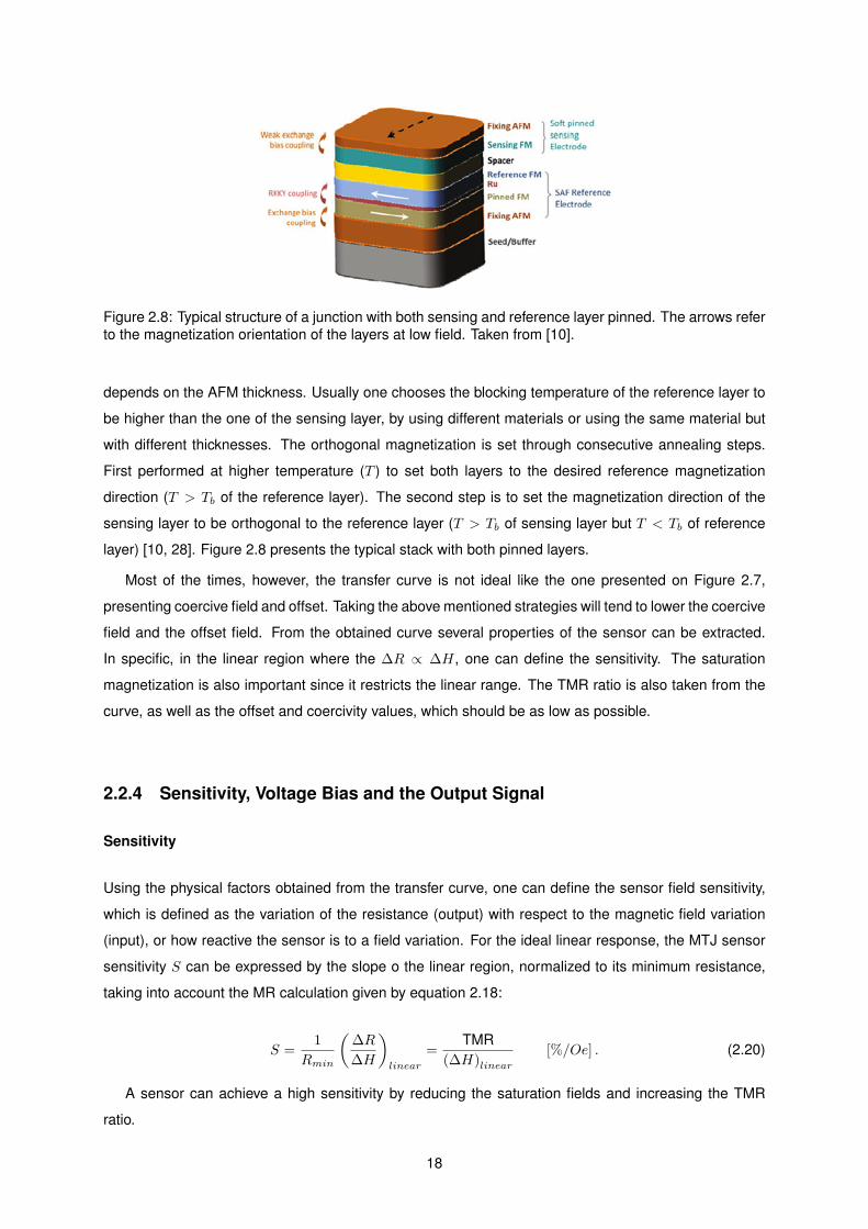
Figure 2.8: Typical structure of a junction with both sensing and reference layer pinned. The arrows referto the magnetization orientation of the layers at low field. Taken from [10].
depends on the AFM thickness. Usually one chooses the blocking temperature of the reference layer to
be higher than the one of the sensing layer, by using different materials or using the same material but
with different thicknesses. The orthogonal magnetization is set through consecutive annealing steps.
First performed at higher temperature (T ) to set both layers to the desired reference magnetization
direction (T > Tb of the reference layer). The second step is to set the magnetization direction of the
sensing layer to be orthogonal to the reference layer (T > Tb of sensing layer but T < Tb of reference
layer) [10, 28]. Figure 2.8 presents the typical stack with both pinned layers.
Most of the times, however, the transfer curve is not ideal like the one presented on Figure 2.7,
presenting coercive field and offset. Taking the above mentioned strategies will tend to lower the coercive
field and the offset field. From the obtained curve several properties of the sensor can be extracted.
In specific, in the linear region where the ∆R ∝ ∆H, one can define the sensitivity. The saturation
magnetization is also important since it restricts the linear range. The TMR ratio is also taken from the
curve, as well as the offset and coercivity values, which should be as low as possible.
2.2.4 Sensitivity, Voltage Bias and the Output Signal
Sensitivity
Using the physical factors obtained from the transfer curve, one can define the sensor field sensitivity,
which is defined as the variation of the resistance (output) with respect to the magnetic field variation
(input), or how reactive the sensor is to a field variation. For the ideal linear response, the MTJ sensor
sensitivity S can be expressed by the slope o the linear region, normalized to its minimum resistance,
taking into account the MR calculation given by equation 2.18:
S = 1Rmin
(∆R∆H
)linear
= TMR(∆H)linear
[%/Oe] . (2.20)
A sensor can achieve a high sensitivity by reducing the saturation fields and increasing the TMR
ratio.
18
Bias Voltage Dependence
The TMR ratio of a MTJ depends on the bias voltage that is applied, being approximately constant for
bias voltages under 30mV, and approximately linearly decreasing until it reaches a value which repre-
sents half of the maximum TMR ratio (TMR0), with a correspondent voltage represented by V1/2. As a
result, the TMR ratio depends on the bias voltage Vb as follows [1]:
TMR(Vb) = TMR0
(1− Vb
2V1/2
). (2.21)
The decrease of the TMR depends on the barrier type, interfaces and the ferromagnetic materi-
als. In particular, the defects in the insulating barrier allow conduction to happen across the barrier for
higher voltages, decreasing the tunneling effect and thus the TMR ratio [29]. Therefore, to minimize the
dependence, a high quality barrier is required.
The sensitivity will also be affected by the voltage bias dependence. Defining S0 as the maximum
sensitivity value obtained for low bias voltages:
S(Vb) = S0
(1− Vb
2V1/2
)(2.22)
If the bias voltage across the barrier is increased to a certain value, the insulator barrier will be
destroyed, with the creation of pinholes, leading to a sudden decrease in the resistance. The breakdown
of the barrier is directly related to the dielectric strength of the insulator, which is the electric field value
E that results in the breakdown of the barrier. This phenomenon occurs for a breakdown voltage Vbreak
whose value is related to E and the thickness of the barrier t. For the typical insulating barriers the
breakdown voltage is on the order 0.5 − 2V . Usually, in practical sensor applications, the breakdown
voltage can be overcome by incorporating an array of MTJ sensors in series. By doing so, a higher
voltage can be applied to the system and it doesn’t compromise the individual sensors.
Output Signal Variation
In the linear region of the sensor’s response, the sensor resistance can be described as the sum of
a nominal resistance R0, at zero magnetic field, and a variation ∆R that, looking at equation 2.20 is
directly related to the variation of the applied magnetic field (with zero magnetic field) H and the sensor
sensitivity S(Vb):
R(H) = R0 + ∆R = R0 + S(Vb)RminH (2.23)
Consequently, the voltage output variation ∆V due to an external magnetic field variation ∆H =
H2−H1, and the current bias I that flows through the MTJ due to the bias voltage applied can be written
as:
∆V = (R (H2)−R (H1)) I = S(Vb)RminI∆H (2.24)
19

A single sensor output can also be given, taking into account its geometry (width W and height h),
its resistance area product (RA) and the angle α between reference and sensing layer magnetization
directions:
∆V = 12TMR(Vb)I
RA
Wh〈cosα〉 (2.25)
Intuitively, a larger area and a thinner barrier thickness lead to a higher number of electrons tunneling
across the barrier, increasing the electrical current that flows in a CPP configuration. So, the resistance
of the sensor will decrease for higher sensor area. Therefore, the resistance area product RA is a
constant parameter and independent of the sensor area. However, this parameter is an intrinsic property
of the tunneling barrier, being highly dependent on the barrier thickness.
20

Chapter 3
System Description and
Characterization
This chapter is focused on a detailed description of the positioning system in development, which has
the objective of reading structures printed with Magnetic Ink. The two main configurations of the sensing
head will be described and simulated. The two considered sensors are characterized for each configu-
ration and the magnetic behavior studied. The second component of the system, which comprises the
magnetic ink structures, is also characterized and present in Appendix ?? (confidential).
3.1 System Description
The aim of this work is to develop a magnetic ink surface scanning device, therefore it has two main
different units: the sensing head with the magnetic sensor and the integrated electronics; and a sample,
where the magnetic structures are printed.
As an interdisciplinary project, the development has input from the different parts: the magnetic
ink is provided by BOGEN Electronics GmbH1, who is also responsible for printing the magnetic ink
structures and developing the integrated electronics as well as the future casing and packaging; and
INESC-MN is responsible for both the characterization of the ink and the development of the sensing
head configuration for the system.
3.1.1 Magnetic Ink
The magnetic ink for this work was available in powder form and printed on various substrates in the
form of periodic structures. It is a ink specifically designed for the MICR application and has both soft
and hard magnetic properties. Further characterization is present in Appendix ?? (confidential).
1http://www.bogen-electronic.com/en/
21

3.1.2 Configurations
To read MI, a constant magnetization of the sample is needed to magnetize or fully saturate the ink.
The magnetization of the ink creates stray fields between the poles created on the structures, which the
magnetic sensor is then capable of measuring. There are mainly three strategies to magnetize the ink
during measurements:
• using a current line, which creates a field that can be used to magnetize the ink;
• using fixed permanent magnets on the substrates; or
• using permanent magnets on the reading head.
According to the objectives of the project the first two strategies are not considered as the solution.
Using a current line requires an extra power source and thus extra electronics on the system. Using
static permanent magnets would increase the complexity of the information storage, and ultimately the
cost. Therefore, the third strategy is considered for this system.
In total six different configurations using magnets were considered for the project. They were named
Standard 1 through 6, or short, Std i (with i=1,...,6). These are represented on Figure 3.1. The con-
figurations were designed taking into account different kinds of magnets (In-Plane (IP) or Out-Of-Plane
(OP) magnetization) and also different ways to magnetize the magnetic bits. Notice that the direction of
movement is always x.
The project in hands has, however, some requirements that exclude a priori some of the configuration
standards. The main requirements are that:
a) it must be able to measure in both directions of movement (−x and +x);
b) the sensor must be placed so that it can be as close as possible to the magnetic ink (bottom of the
sensing head); and
c) for simplified electronics, the magnetic sensor should be able to create alternating North and South
poles.
As a result, Std 2, Std 4, Std 5 and Std 6 are excluded. To measure a saturated magnetized bit the
magnet should magnetize during or shortly prior to the sensor passage, but Std 5 and Std 6 only allow
the magnetization of the ink in one direction of movement (+x), therefore not complying with requirement
a). The other two configurations magnetize the ink in a perpendicular direction to the movement of the
reading head. By doing so, no alternating poles are created. It comes that only Std 1 and Std 3 (Figures
3.1a and 3.1c respectively) are considered in this work for the development of a reading head for the
proposed system.
A set-up scheme of the system is presented on Figure 3.2a, on which two magnets are placed on
each side of the sensor and the scan is done in the x direction. The sensor is sensitive in the y0z plane
and the field created by the magnets in the region of the sensor is perpendicular (in the x direction) to
the sensitive plane in order to avoid influence on the sensor’s magnetic behavior. On the region of the
MI structures, the magnetic field from the magnets (in blue) create a magnetization on the ink line in the
x direction. This magnetization is responsible for the creation of the stray field which is measured by the
22

(a) Ink magnetized on the x direction. 2 magnets withOOP magnetization. Sensor’s sensitive plane parallel tomagnets.
(b) Ink magnetized on the y direction. 2 magnets withOOP magnetization. Sensor’s sensitive plane parallel tomagnets.
(c) Ink magnetized on the x direction. 2 magnets with IPmagnetization. Sensor’s sensitive plane parallel to mag-nets.
(d) Ink magnetized on the y direction. 2 magnets with IPmagnetization. Sensor’s sensitive plane parallel to mag-nets.
(e) Ink magnetized on the x direction. Magnet with OOPmagnetization. Sensor’s sensitive plane perpendicular tomagnets.
(f) Ink magnetized on the x direction. Magnet with OOPmagnetization. Sensor’s sensitive plane parallel to mag-nets.
Figure 3.1: Configuration standards considered for the project.
sensor. Notice that by measuring the z component of the ink line’s field it is possible to measure north
and south poles in consecutive borders of the structures. The presence of two magnets (one passing
before and another after the point of interest) allow the measurement of both directions of movement
(−x and x). It is important to define some geometrical variables, which is done on Figure 3.2b. The
23

(a) Conceptual scheme of the set-up for the system.(b) Definition of the geo-metrical variables.
Figure 3.2: Proposed concept for the system.
variable a indicates the shift between the sensor and the magnets’ bottom line; the variable b indicates
the distance between the magnets, with the sensor always placed at b/2. The Reading Distance (RD) is
introduced, which is the distance in z from the top of the magnetic ink bit and the sensor.
In this work two kinds of permanent magnets (PMs) with the same dimensions but with different
magnetization direction were used, in accordance with the configuration standards Std 1 and Std 3
from Figure 3.1. The PMs are characterized by three main parameters: the dimension, the relative
permeability of the material µr and the remanence (or remanent flux density) Br. The latter is related
to the magnetization of the magnets at zero applied external magnetic field, and is commonly described
as the maximum magnetic flux created by the PM. Taking into account the geometry and coordinate
system on Figure 3.1 and the physical values of the magnets given by the manufacturer (supermagnete
[30]), the parameters considered for these magnets are:
Magnet Geometry (mm3) µr Br (T) Direction ofMagnetization
OOP Magnetization 1×10×4 1.05 1.43 xIP Magnetization 1×10×4 1.05 1.43 z
Table 3.1: Physical parameters of the magnets used.
The holders for the magnets are fabricated using a conventional 3D printer. The holders are designed
using a technical drawing tool, in specific AutoCAD. Due to restrictions in the assembly of PCB plus
magnet holders, on both configurations the separation between the magnets is b = 6 mm.
3.1.3 Simulation of the Magnets Configurations
Both Std 1 and Std 3 presented on Figures 3.1a and 3.1c were simulated using the software COMSOL
Multiphysics, which is a finite element modeling (FEM) tool. In this software the 3D geometry of the po-
sition of the magnets is designed and the module Magnetic Fields, No Currents (mfnc) is used. The field
created by the magnets is computed by using the remanent flux density Br and defining the magnetic
24

flux conservation on all space. Inside the magnets the magnetic flux density B and the magnetic field H
are related by the constitutive relation
B = µ0µrH + Br,
being µr and Br the parameters of the magnets, whose values are resumed in Table 3.1. Even though
only the magnetic field created by the magnets is simulated, it allows the evaluation of the field created at
any given point of the space defined, therefore allowing the prediction of the effectiveness of magnetizing
the ink as well as of the influence on the sensor.
On Figure 3.3a the 3D geometry is shown with the magnet dimensions, for both configuration sim-
ulations (both kinds of magnets have the same dimensions). The simulation results are shown in a 2D
plane, which is a slice from the 3D geometry simulation. This slice is the plane x0z at y = 0 mm, which
corresponds to the center symmetry plane of the geometry, as seen in Figure 3.3b.
(a) 3D geometry of the simulated configurations. (b) 2D plane slice, where the results are shown.
Figure 3.3: 3D geometry used on the simulation software. Geometry of the magnets: 10×4×1 mm3;b = 6 mm.
OOP Magnetization - Std 1
The first simulation was done for the configuration of Figure 3.1a, on which the magnets are magnetized
in the x direction. A vector field plot was first done to evaluate the direction of the magnetic field in space.
Figure 3.4 shows the resulting plot. The vectors are plotted in a logarithmic scale, as the interest lies in
determining which components are present and not what the strength of the field is.
There are mainly two areas of interest: around the sensor, which is ideally placed at the point (x, z) =
(0,-2) mm; and on the area where the magnetic ink structure is being magnetized for measuring, which
is at any z below z = -2 mm and between x = -5 mm and x = 5 mm.
Immediately it is noticed that on the region where the MI structures is measured (x=0) the field is
very weak and the x component, which is the most important for magnetizing the ink is almost non-
existent. The only regions where the ink is magnetized in the x direction are right below each magnet.
25

Figure 3.4: Magnetic field vectors (in logarithmic scale) for the magnets with OOP magnetization. Thenumbered lines represent the regions where further studies are done.
If soft magnetic ink is used for the structures, the magnetization of the ink could not hold time enough
to be measured at x=0. Futhermore, in the area where the sensor is placed, the field is not purely
and uniformely perpendicular to the sensing plane y0z. A component on the z direction, which is the
sensitive direction of the sensor, is easily seen, thus predicting some influence on the sensor magnetic
behavior. On the same plot three lines are drawn, this lines indicate three regions where the magnetic
field components are studied. These lines are:
1. from the center point between the magnets to 6 mm below this point: from z = 0 mm to z = -6 mm
with fixed x = 0 mm;
2. from the inner pole of the left magnet to the inner pole of the right magnet at the height where the
sensor is placed: from x = -3 mm to x = 3 mm with fixed z = -2 mm;
3. a span of 10 mm where the MI structures are located (if at 2 mm Reading Distance): from x = -5
mm to x = 5 mm with fixed z = -4 mm.
On each line, from one tip to the other a line plot is done of the magnetic field components. The plots
are presented on Figure 3.5.
On Figure 3.5a the three components of the field are plotted along Line 1. Along this axis the y and
z components of the field remain constant and null whilst the x component suffers variation. Since the
latter component of the field is the one that has no effect on the magnetic behavior of the sensor, the
sensor should be placed on this axis, so as expected the sensor must be placed at b/2 - half the distance
between the magnets.
On Figure 3.5b, where the three components of the flux are plotted along Line 2, this placement is
once more seen as the best. The y component along this line suffers no change and remains null. The
x component is constant and different from 0 but since it is perpendicular to the sensor sensitive plane,
no influence from this component is expected. However, around the point where the sensor should be
placed, the z component of the field has some variation. Since the z component lies on the sensitive
26
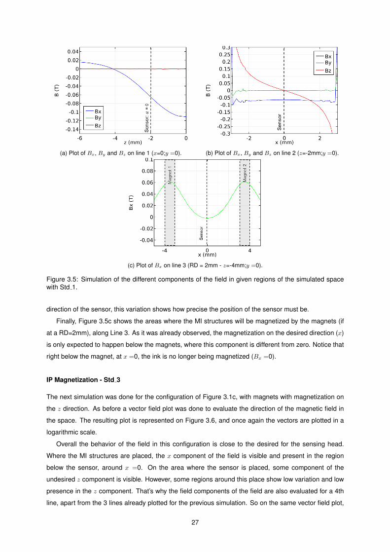
(a) Plot of Bx, By and Bz on line 1 (x=0;y =0). (b) Plot of Bx, By and Bz on line 2 (z=-2mm;y =0).
(c) Plot of Bx on line 3 (RD = 2mm - z=-4mm;y =0).
Figure 3.5: Simulation of the different components of the field in given regions of the simulated spacewith Std 1.
direction of the sensor, this variation shows how precise the position of the sensor must be.
Finally, Figure 3.5c shows the areas where the MI structures will be magnetized by the magnets (if
at a RD=2mm), along Line 3. As it was already observed, the magnetization on the desired direction (x)
is only expected to happen below the magnets, where this component is different from zero. Notice that
right below the magnet, at x =0, the ink is no longer being magnetized (Bx =0).
IP Magnetization - Std 3
The next simulation was done for the configuration of Figure 3.1c, with magnets with magnetization on
the z direction. As before a vector field plot was done to evaluate the direction of the magnetic field in
the space. The resulting plot is represented on Figure 3.6, and once again the vectors are plotted in a
logarithmic scale.
Overall the behavior of the field in this configuration is close to the desired for the sensing head.
Where the MI structures are placed, the x component of the field is visible and present in the region
below the sensor, around x =0. On the area where the sensor is placed, some component of the
undesired z component is visible. However, some regions around this place show low variation and low
presence in the z component. That’s why the field components of the field are also evaluated for a 4th
line, apart from the 3 lines already plotted for the previous simulation. So on the same vector field plot,
27

Figure 3.6: Magnetic field vectors (in logarithmic scale) for the magnets with IP magnetization. Thenumbered lines represent the regions where further studies are done.
four lines are represented, showing where the evaluation of the different components were done. The
lines are:
1. from the center point between the magnets to 6 mm below this point: from z = 0 mm to z = -6 mm
with fixed x = 0 mm;
2. from the inner pole of the left magnet to the inner pole of the right magnet at the height where the
sensor is placed: from x = -3 mm to x = 3 mm with fixed z = -2 mm;
3. a span of 10 mm where the MI structures are located (if at (2-a) mm Reading Distance): from x =
-5 mm to x = 5 mm with fixed z = -4 mm.
4. from the inner pole of the left magnet to the inner pole of the right magnet at the height where the
sensor is placed in a configuration with a = 0.5 mm: from x = -3 mm to x = 3 mm with fixed z =
-2.5 mm;
Figure 3.7 shows the components of the magnetic field plotted on the defined Lines 1, 2 and 3.
On Figure 3.7a the three components of the field are plotted along Line 1. Once more, along this
axis the only non-zero component of the field is Bx, while both By and Bz, which are in the sensitive
plane of the sensor are null. Therefore, the sensor should be placed on this axis.
On Figure 3.7b, for Line 2 the same behavior is again observed, the x component is non-zero, but
it is not expected to influence the sensor. Both By and Bz are zero half way between the magnets.
However, once more, the z component has some variation around this point, requiring thus very precise
positioning at this point.
Finally, on Figure 3.7c Bx is plotted on Line 3 and it is clearly seen that the ink is magnetized in the
x direction, right below the sensor. Therefore expecting a more efficient magnetization of the ink during
measurement.
Since it was observed on Figure 3.6 that by increasing the distance between the sensor and the
bottom line of the magnets, a, the magnetic field seems to be more uniform and purely on the x direction,
28
(a) Plot of Bx, By and Bz on line 1 (x=0;y =0). (b) Plot of Bx, By and Bz on line 2 (z=-2mm;y =0).
(c) Plot of Bx on line 3 (RD = 2-a mm; z=-4mm;y =0).
Figure 3.7: Simulation of the different components of the field in given regions of the simulated spacewith IP magnetization magnets.
Figure 3.8: Plot of Bx, By and Bz on line 4. Sensor at a = 0.5 mm.
the three components of the field are plotted on this Line 4 and presented on Figure 3.8. As expected
from the vector plot, the z component of the field has very low variation around the position of the sensor
(in the middle), being zero both ways for 1 mm (between x =-1mm and x =1mm). So, by lowering
the sensor by 0.5 mm - a = 0.5 mm - on the configuration, the position needs not be so precise and
therefore less influence from the magnets is expected.
29

3.2 Sensing Head Characterization
3.2.1 Magnetoresistive Sensors
In this work, two TMR sensors with different geometries were considered. Both consisting of an array of
MTJs in series. The stack of each MTJ has a soft pinned sensing layer, which is a linearization strategy
described on section 2.2.3. The stack is as follows and graphically described on Figure 3.9a:
• [Ta 5/CuN 25] × 6/ Ta 5/ Ru 5/ Ir20Mn80 20/ Co70Fe30 2/ Ru 0.85/ Co40Fe40B20 2.6/ MgO ≈ 1/
Co40Fe40B20 2/ Ta 0.21/ Ni80Fe20 4/ Ru 0.20/ Ir20Mn80 6/ Ru 2/ Ta 5/ Ru 10,
being the thickness represented in nm and the alloy compositions in %. The barrier thickness was
optimized for a resistance-area product of 20 kΩµm2, deposited in a Singulus Timaris sputtering tool at
INL, on a thick silicon wafer covered with an SiO2 layer of 1 µm. The sensors were then microfabricated
at INESC-MN by a combination of lithography (DWL) and etching (Nordiko 3600) patterning techniques
[31]. Notice that the reference and the free layer are not pinned by a simple AFM layer. In this stack
a SAF and a SF are used as the pinning layers, both described in section 2.2.2. The annealing steps
required during the fabrication process are the same used as described in section 2.2.3, where two
different annealing at different temperatures must be done to set the perpendicular directions on the
different pinning layers. The sensors chosen vary in number of elements and on the junction area,
therefore having different spatial resolutions:
• Sensor S1 is an array of 72 sensing elements (MTJs) with an individual area of 50×50 µm2
distributed along 8 columns and 9 rows occupying a total area of 525×570 µm2 to maximize the
SNR [32];
• Sensor S2 is an array of 4 sensing elements (MTJs) with an individual area of 10×4 µm2 dis-
tributed along 4 columns and 1 row occupying a total area of 58.5×4 µm2.
Each array is represented in a schematic way in Figure 3.9b. The sensor chips were diced and wire-
bonded onto a rigid PCB (printed circuit board) designed for the measuring system (see chapter 5).
Consequently the magneto-transport curves (R(H)) were measured.
3.2.2 Magneto-transport Characterization Tool
As it was seen in Chapter 2, a MTJ sensor is characterized by its magnetic transfer curve. The same
goes for an array of MTJs as in the present work. By measuring the resistance of the sensor as a
function of the applied magnetic field (R(H)), the transfer curve is obtained and the relevant physical
values taken.
The 140 Oe setup is a magneto-transport measuring tool. It is composed of a pair of Helmoltz coils
powered by a current source; four micro-positioning Tungsten needle probes with spatial resolution of
about 10 µm, which can be connected to a current source (bias current) and a voltmeter; a microscope;
and a controlling/acquisition software. The Helmoltz coils are separated by an optimized distance taking
30

(a) Thin film structure of the used MTJ pillar. (b) Scheme of the arrays of sensors S1 and S2.
Figure 3.9: MTJ pillar structure and scheme of the junction array of sensors S1 and S2.
into account the current supplied so that in the center region between the coils an uniform magnetic
field (H) is created in a range between -140 Oe and 140 Oe, or considering B = µ0H (valid in air),
between -14 mT and 14 mT. The controlling of the setup is done using a computer software and the
communication through GPIB communication. The user can control the current bias for the sensors;
the magnetic field sweep range, limited to the setup’s range; the steps during the sweep; the number of
voltage points averaged per H applied; and the stabilization time at each measurement. The magnetic
field sweep is done from minimum to maximum and then back to minimum so that a complete magnetic
transfer curve is obtained. This setup allows also for a bias current sweep is also possible.
The measurement in this work is done by using just two of the four probes, with fixed current bias.
The current is applied in a CPP configuration and a voltage is taken from the terminals. The current
is applied in series and the voltage measured in parallel. By connecting the voltmeter to the terminals
where the current is injected, the voltage is collected and the resistance computed through Ohm’s Law.
The computer software acquires directly the voltage values and makes an initial data treatment allowing
the user to see the transfer curve in real time while the sweep is done.
3.2.3 Magnetotrasport Characterization
System with no magnets
First a reference transfer curve for both sensors S1 and S2 is measured. Since the considered system
has magnets to magnetize the MI, it is expected that cross fields from the magnets influence the sensor,
in particular components of the field laying IP with the sensor’s sensing plane. So as a comparison
and a reference, the transfer curves of both sensors S1 and S2 with no magnets present on the system
were obtained and presented in Figures 3.10a and 3.10b. The current bias used was of 100 µA for
31

S1 and 50 µA for S2. In the linear range 20 points per mT were taken. From the transfer curves, the
important characteristic values are taken, in specific the MR ratio, the minimum resistance (Rmin), the
sensitivity around zero applied magnetic field (S0), the shift of the center of the linear region (µ0Hf) and
the coercivity (µ0Hc).
(a) Sensor S1. (b) Sensor S2.
Figure 3.10: Reference transfer curves of sensors S1 and S2, without magnets present on the system.
Sensor S1 has a 542 Ω minimum resistance, with a TMR of 129%, which is limited by contact
resistance due to the high number of MTJs in series, and a linear linear response within a ±2 mT range
(around zero applied field) with a non-hysteric behavior (low coercivity). A sensitivity of 15.1 V/T is
achieved for a bias current of 100 µA.
Sensor S2 has has a 1187 Ω minimum resistance, with a TMR of 156%, and a linear linear response
within a ±2 mT range with a non-hysteric behavior (low coercivity). A similar sensitivity of -14.2 V/T is
achieved for a bias current of 50 µA.
System with OOP magnetization magnets (Std 1)
The first transfer curves measurements were done using the magnets with OOP magnetization, corre-
sponding to Std 1 configuration of Figure 3.1a. From the simulations it is easily seen a big variation
on the z component of the field around the area where the sensor is placed (Figure 3.5). Therefore,
it is expected that if the sensor is not exactly centered between the magnets, a big influence from the
magnetic field will be evidenced in the transfer curve of the sensor.
First, sensor S1 was measured in this configuration. It was observed that the transfer curve would
be different between measurements, being almost non-reproducible. Any change in the relative position
between both the magnets and the sensor changes in some way the transfer curve. And such a change
can easily happen with time, mounting or usage. Figure 3.11 shows the transfer curves obtained for this
sensor using this configuration Std 1. All transfer curves were performed with a bias current of 100 µA
and in the linear region 20 points per mT were taken.
Between different measurements always some properties changed in particular the sensitivity value.
It is seen on Figure 3.11 four different curves used for measurements, which although with similar in-
32
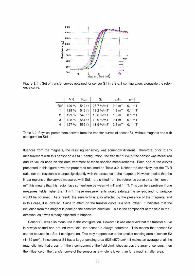
Figure 3.11: Set of transfer curves obtained for sensor S1 in a Std 1 configuration, alongside the refer-ence curve.
MR Rmin S0 µ0Hf µ0Hc
Ref 129 % 542 Ω 27.7 %/mT 0.4 mT 0.1 mT1 129 % 546 Ω 19.2 %/mT 1.3 mT 0.1 mT2 129 % 546 Ω 16.6 %/mT 1.8 mT 0.1 mT3 128 % 551 Ω 13.9 %/mT 2.1 mT 0.1 mT4 127 % 552 Ω 11.9 %/mT 2.6 mT 0.1 mT
Table 3.2: Physical parameters derived from the transfer curves of sensor S1, without magnets and withconfiguration Std 1.
fluences from the magnets, the resulting sensitivity was somehow different. Therefore, prior to any
measurement with this sensor on a Std 1 configuration, the transfer curve of the sensor was measured
and its values used on the data treatment of those specific measurements. Each one of the curves
presented in this figure have the properties resumed on Table 3.2. Neither the coercivity, nor the TMR
ratio, nor the resistance change significantly with the presence of the magnets. However, notice that the
linear regions of the curves measured with Std 1 are shifted from the reference curve by a minimum of 1
mT, this means that this region lays somewhere between -4 mT and 1 mT. This can be a problem if one
measures fields higher than 1 mT. These measurements would saturate the sensor, and no variation
would be obtained. As a result, the sensitivity is also affected by the presence of the magnets, and
in this case, it is lowered. Since th effect on the transfer curve is a shift (offset), it indicates that the
influence from the magnet is done on the sensitive direction. This is the component of the field in the z
direction, as it was already expected to happen.
Sensor S2 was also measured in this configuration. However, it was observed that the transfer curve
is always shifted and around zero-field, the sensor is always saturated. This means that sensor S2
cannot be used in a Std 1 configuration. This may happen due to the smaller sensing area of sensor S2
(4×59 µm2). Since sensor S1 has a larger sensing area (525×570 µm2), it makes an average of all the
magnetic field that cross it. If the z component of the field diminishes across the array of sensors, then
the influence on the transfer curve of the sensor as a whole is lower than for a much smaller area.
33

System with IP magnetization magnets (Std 3)
Using the magnets with IP magnetization (in the z direction) corresponding to the configuration Std 3
represented in Figure 3.1c, a further study was done on the transfer curves, also taking into account the
results obtained in the simulations on section 3.1.3.
First, using sensor S1 and with a = 0 mm a series of three transfer curves were measured (Figure
3.12b). Making a = 0.5 mm the same number of transfer curves were also measured (Figure 3.12a).
All measurements were performed with a bias current of 100 µA and with a step of 20 points per mT
on the linear range of the curve. By doing several measurements, with some time between them, the
consistency of the configuration can be tested.
(a) a = 0 mm. (b) a = 0.5 mm.
Figure 3.12: Study on the transfer curves of sensor 1, with configuration standard Std 3.
It is observed that compared with Std 1 measured previously, a much greater consistency is obtained:
the coercivity, the offset of the curve and the TMR ration suffer almost no changes between measured
transfer curves, nonetheless they differ a bit from the reference curve. Furthermore and in accordance
with simulations it is also noticeable much better transfer curves with a = 0.5 mm, i.e., curves with
a linear behavior around zero applied field and with low coercivity. Therefore for the measurements
done using this configuration the values used for the sensor are the ones with a = 0.5 mm. The same
conclusions on the geometry were made for sensor S2 as well.
On Figure 3.13a the transfer curve is presented for sensor S1 in a Std 3 configuration with a =
0.5 mm. Figure 3.13b shows the resulted curve for sensor S2. The values taken from the curves are
presented and resumed in table 3.3.
Looking at the obtained transfer curve for sensor S1, notice that comparing the obtained curve and
the reference curve, still some influence from the magnets’ magnetic field is observed. The sensitivity
around zero applied field is the most influenced, being decreased by almost half. The offset of the curve
suffers almost no change from the reference curve, so the component of the field that influences the
sensitive direction (z component) is not the one that has the most influence, but the sensitivity is still
altered. This is due to cross fields in the other direction of the sensitive plane (y direction), which will
affect it by increasing the linear range (and not the MR) and so, decreasing the overall sensitivity.
34

(a) Sensor S1. (b) Sensor S2.
Figure 3.13: Transfer curves for the sensor S1 and S2, with configuration Std 3 and a = 0.5 mm.
When it comes to sensor S2, The major influence on the curve seems to be a bigger shift in the
curve. Again, since sensor S2 has a smaller area, it is more prone to be affected by cross fields present
in the region of the sensor. The average on sensor S1 seems to nullify the presence of the cross field in
z, which doesn’t happen for S2. The resulting sensitivity is however higher in the presence of magnets
than it is for sensor S1.
MR Rmin S0 µ0Hf µ0Hc
Sensor S1No Magnets 129 % 542 Ω 27.7 %/mT 0.4 mT 0.1 mT
With Magnets 131 % 542 Ω 14.3 %/mT 0.8 mT 0.1 mT
Sensor S2No Magnets 156 % 1187 Ω -22.2 %/mT 0.4 mT 0.2 mT
With Magnets 159 % 1161 Ω -24.4 %/mT 1.3 mT 0.3 mT
Table 3.3: Physical parameters derived from the transfer curves of sensors S1 and S2, without magnetsand with configuration Std 3 and a = 0.5 mm.
35

36

Chapter 4
Hard Magnetic CoCrPt Structures
In this chapter a strategy to validate the used sensors is developed, by measuring well defined and
well-known structures and comparing with simulation. First the fabrication process of these structures
is explained in detail, along with the characterization of the fabricated samples. Afterwards a simulation
model of the structures is proposed.
4.1 Micro-Fabrication
The samples fabricated in this work were designed to have a periodic signal with alternating north
and south pole. The structure can be seen in Figure 4.1, where the bits have a length named pole-
pitch (PP) and are equally spaced with this same length. The material used for the structures is a
hard ferromagnetic alloy CoCrPt. The micro-fabrication process of the structures is fairly simple. It
has just four steps: alloy deposition, pole definition, excess material etching and finally setting of the
magnetization direction. Each one of the steps of this process are described with some detail in the
following sections. The run-sheet of the process can be found in Annex A, where also the AutoCAD
masks and pictures of the samples throughout the fabrication can be found.
Figure 4.1: Structure of the micro-fabricated CoCrPt structures.
Three different CoCrPt structures were designed for this project differing in the pole-pitch and the
number of consecutive structures: 240 µm, 320 µm and 1000 µm with 35, 26 and 8 structures respec-
tively. The width W of all the structures is of 3 mm and the thickness of 1000 A.
37

4.1.1 Deposition by Magnetron Sputtering
The first step of the structures fabrication is the deposition on glass substrates of CoCrPt alloy, a mag-
netic alloy. This is done using sputter deposition, and in specific DC magnetron deposition [33].
DC planar magnetron discharges are widely used for sputter deposition of metallic thin films such
as aluminum, copper, gold and various alloys. When powered by an RF source it is also used for
sputter deposition of insulating materials. In this deposition technique the target, where the material to
be deposited is located, has a negative bias voltage while the chamber and shield are grounded. In a
given threshold (some hundred Volts) this bias voltage creates the discharge in the inert gas injected
in the chamber creating positive ions (such as Ar+) that are accelerated towards the target, being the
remaining electrons used for further discharge. In magnetron sputtering a concentric DC magnetic
field is created at the target using permanent magnets. This leads to a confinement of the secondary
electrons increasing the ionization probability, therefore more positive ions are accelerated resulting thus
in higher sputtering rates. This technique has nonetheless a side effect on which the the target wear
is more pronounced in a concentric ring (where the magnetic field lines close), forming a groove and
resulting in deposition rate changes through time. The difference between using DC or RF power supply
lies in the type of material. To deposit insulating materials with this technique, an RF source must be
used since the insulating material does not allow neutralization of the incident positive ions.
Sputtering tool - Alcatel SCM450
In this work a DC magnetron sputtering technique is used to deposit the CoCrPt alloy. The tool used is
the Alcatel SCM450, which has a deposition chamber represented in Figure 4.2. This chamber has three
magnetrons where 4 inch targets can be placed. Three independent shutters can be used to cover the
targets. This machine has no load-lock, so the loading and unloading of the samples requires venting
the chamber. The chamber has also four stations for 3 inch wafer holders, three of which are water-
cooled. A base pressure of 10−6 or less is achievable 24 hours after pump down with a turbomolecular
pump. The chamber pressure during the process is uncontrollable by the user and directly dependent
on the gas (Ar) flow.
In this work two depositions of CoCrPt were done. First, a calibration sample to confirm the deposition
rate of 6.48 A/min, determined in a different process, described in [35]. After the deposition rate was
confirmed by using a profilometer technique (see the run-sheet in Annex A), the final sample deposition
of 1000 A of the alloy was done. On Table 4.1 the parameters used and observed on both the depositions
are resumed.
SampleBase
Drive BiasChamber
Ar flowDeposition Total
Pressure Pressure Rate Time
Calibration 1.62×10⁻⁶ Torr 40 WRF 820 V 2.14 mTorr 20 sccm 6.48 A/min 154 minFinal Sample 3.60×10⁻⁶ Torr 40 WRF 800 V 2.12 mTorr 20 sccm 6.48 A/min 154 min
Table 4.1: Parameters for sputter deposition of CoCrPt using Alcatel SCM450.
38

Figure 4.2: Schematic view of the deposition chamber of Alcatel SMC450. Taken from [34].
4.1.2 Pole Definition by Litography
Lithography is usually the first step of pattern transfer in micro-fabrication. A photo-sensitive polymer
(photoresist) is coated on the sample, which is then exposed to light with a certain wavelength. It
comprises three main steps: photoresist (PR) coating; lithography; and finally development.
PR Coating
First of all the sample is subjected to a pre-treatment in the Vapor Prime oven, where a surface purge
is performed and an organic compound, HMDS, is sparayed over it at 130°C in vacuum. This additional
initial step improves the adhesion of the PR on the material’s surface due to the affinity of the PR to
certain chemical groups of the HMDS.
A positive PR is then coated on the sample. A 1.5 µm thickness is aimed for by defining the proper
spinning velocity during coating, which for this specific PR is of 2500 rpm. Afterwards it is baked at
100°C for 1 min. This allows the evaporation of the solvents and further improves the uniformity of the
coated PR.
Photo-Lithography
In this step a laser is swept over the area to be exposed, turning on and off as defined by the mask,
whose design is to be transferred to the material. The laser has a specific wavelength, which breaks
the chemical bonds of a positive polymer increasing its solubility, and strengthens the chemical bonds
of a negative PR. The areas exposed are chosen depending on the type of PR, whether it is positive or
negative, and on what is the posterior use, whether the next process steps comprise etch or lift-off.
The design transfer is performed by a Direct Write Laser system - Heidelberg DWL 2.0. It uses a
diode laser with wavelength of 405 nm, and the pattern is designed by stripes of 20 µm. This system has
39

a maximum feature resolution of 0.8 µm, which corresponds to the laser spot size, and has an alignment
precision of 0.1 µm, which corresponds to the resolution of the x-y stage.
In this work, a positive PR is used and the next step on the process is an etching step, on which
the unwanted deposited alloy is removed. Therefore the mask to be transferred is given to the control
software of the DWL as an Inverted mask, which means that the only unexposed areas are the ones
that comprise the poles of the designed track.
PR Development
After the Lithography step, the exposed PR is removed in a development step. The sample is first baked
at 110°C for 1 min, so that the chemical reactions started by the laser exposure stop. After cooling down,
the sample is subject to a certain developer solution designed to dissolve the areas that were exposed
by the laser, while the unexposed regions remain intact.
After development, the PR on top of the deposited CoCrPt alloy has the shape of the desired struc-
tures, protecting the material which is not to be removed.
4.1.3 Etching by Ion-Milling
The last step for the structure definition is the etching of the unwanted material - the material that is not
protected by the remaining PR from the last step.
In this work an etching by an Ion-Milling technique is used. It is a strongly directional and non-
selective etching process. It is based on the bombardment of high energy ions (in this case Ar+), which
remove the unprotected material solely by physical impact.
Ion-Milling tool - Nordiko 3000
The machine used for the etch is Nordiko 3000, which is an automated ion beam deposition and milling
system for up to 6 inch wafers. For this work only the milling system is of interest, which uses only the
assist/etch gun, which is the source of the high energy ions beam, and the sample holder. The holder is
water-cooled and can be positioned with an angle between 0° and 80° in relation to the etch gun source.
This gun has 25 cm diameter and is directed to the sample holder. A plasma is created inside the gun
and a voltage difference is applied on the beam exit grids making it responsible for accelerating the
ions. The removal of the material is done with a controlled etch rate and a well defined incident angle,
which allow the control of the profile on the borders of the etched material. The sample holder is also in
constant rotation, thus ensuring uniformity of the etching.
To define the poles on the sample, the material that is not protected by the PR is completely removed
down to the substrate. The etch is performed at an angle of 70° and with a rotation speed of 40 rpm.
Before the process the chamber reaches a base pressure of 7.8×10⁻⁷ Torr. An etching rate of 0.8 A/s
was considered. On table 4.2, the conditions of the performed etching are resumed.
40

Power Voltage + Current + Voltage - Current - Ar Flux Pan Rotation Time
53 W 488.3 V 28.7 mA 194.3 V 1.7 mA 7.9 sccm 70° 40 rpm 1250 s
Table 4.2: Parameters for etching of CoCrPt using Nordiko 3000.
4.1.4 Magnetization Definition
The last step on the micro-fabrication process of these structures comprises the definition of the direction
of the magnetization on the structures, so that the desired alternating poles are created.
Being a magnetic alloy, there is no need to anneal the sample, since it already shows magnetic
behavior as deposited. Therefore, in principle, only a strong magnetic field in the desired direction
needs to be applied. However, in this work an anneal was done in the presence of a strong magnetic
field. The high temperature, together with the strong magnetic field organizes the structure of the film
and maintains the magnetization. Notice that thermal annealing is not usually done on this alloy, and as
such some study on the effect of this step needs to be done. Since, in this work not such a study was
done, the tracks produced and used ended up being the ones annealed.
Annealing Setup
The annealing of the samples was done in a setup, on which the magnetic field is applied during a
complete thermal cycle. This setup comprises of a sample holder, for up to 1×1 inch2 square samples;
and a pair of Helmoltz coils, whose current and distance between the cores define the intensity of the
applied field, with a maximum value of 0.5 T. The heating of the sample is done using a halogen lamp,
also calibrated so that the user knows which temperature to set. The annealing is performed in vacuum,
with a pressure of below 10−6 Torr.
For this sample the annealing was done with a temperature of T =350°C for 2 hours with an applied
field of 0.5 T.
4.1.5 Magnetic Properties Measurement - Vibrating Sample Magnetometer
The Vibrating Sample Magnetometer (VSM) is a characterization technique of the magnetic properties
of magnetic materials. The sample is mounted on the tip of a rod, which vibrates around the vertical
axis. It is located and displaced in an uniform field region, created by Helmoltz coils. The flux changes
created by this movement produces in a second set of coils - the pick-up coils - a signal (V ) proportional
to the magnetic flux (φ) rate variation V ∝ dφ/dt. The voltage signal is then fed to a lock-in amplifier,
which uses the vibrating frequency of the rod as reference.
The VSM tool allows the measurement of the hysteresis loops of the material, which are measure-
ments of the magnetic moment as a function of the applied magnetic field.
After annealing the magnetic properties of the sample were obtained using VSM. The field on the
VSM was applied parallel to the direction defined at the annealing and the hysteresis loop of magnetic
moment vs. applied field was obtained. By knowing the volume of the sample, the magnetization was
41
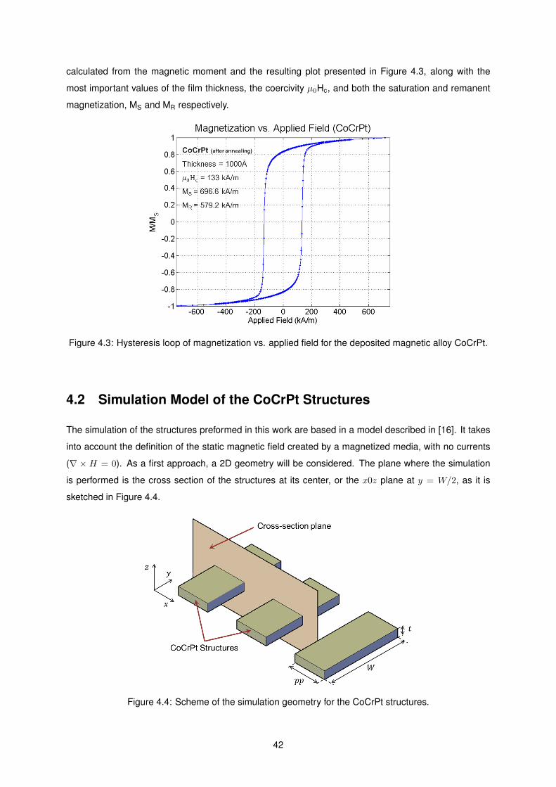
calculated from the magnetic moment and the resulting plot presented in Figure 4.3, along with the
most important values of the film thickness, the coercivity µ0Hc, and both the saturation and remanent
magnetization, MS and MR respectively.
Figure 4.3: Hysteresis loop of magnetization vs. applied field for the deposited magnetic alloy CoCrPt.
4.2 Simulation Model of the CoCrPt Structures
The simulation of the structures preformed in this work are based in a model described in [16]. It takes
into account the definition of the static magnetic field created by a magnetized media, with no currents
(∇ × H = 0). As a first approach, a 2D geometry will be considered. The plane where the simulation
is performed is the cross section of the structures at its center, or the x0z plane at y = W/2, as it is
sketched in Figure 4.4.
Figure 4.4: Scheme of the simulation geometry for the CoCrPt structures.
42

4.2.1 Magnetic Field from a Flat Surface - 2D Model
In 2D, assuming no variation in any properties in the track direction, the magnetic field defined in equation
2.16 can be integrated as:
H(r) = − 12π
∫S
d2r′ (∇ ·M(r′)) r− r′
|r− r′|2 + 12π
∫P
dr′ (M(r′) · en) r− r′
|r− r′|2 , (4.1)
where as before r− r′ is the vector between a point in the magnetized material (r′) and the point where
the field is calculated (r). The integration over the volume poles becomes an area integration (S) over
the (x, z) plane projection of the sample volume. The surface integral becomes a line integral (P ) around
the projected area. The position vector is thus now r = (x, z).
Figure 4.5: Ilustration of the derivaton of the magnetic field from a 2D line of constant charge. Adaptedfrom [16].
If one considers plane surfaces, or lines in 2D, with constant pole density (∇ ·M(r′) = 0), a sim-
plification can be made. The line, corresponding to the surface, lies on the z axis (Figure 4.5), and let
the vector r′ − r be described by the complex variable ω = x + iz. Denoting σm as the surface charge
density, and using the second term of 4.1, the field can be written from
H∗ (ω) = iσm2π
∫ ω2
ω1
dω′ · (ω − ω′)|ω − ω′|2
= iω
2π log(ω − ω2
ω − ω1
), (4.2)
where ω1 and ω2 are the tip coordinates of the 2D surface as can be seen in the scheme of Figure 4.5,
and H∗ (ω) is the complex conjugate of the field
H (ω) = Hx (x, z) + iHz (x, z) . (4.3)
By writing the complex variable in polar coordinates ω = r expiθ, the obtained field in terms of these
coordinates is
H (r, θ) = −σm2π
(∆θ + i log
(r2
r1
))= Hn + iHt, (4.4)
yielding a normal (Hn) and tangential (Ht) field to the magnetized surface. And being r1 and r2 the
distances to the corners of the surface line, and ∆θ the subtended angle.
43

4.2.2 Two-Dimensional Field from the CoCrPt Sample
In this work, the alloy structures are magnetized in the x direction, therefore both the surfaces on the y0z
plane of each line contribute to the calculation of the field. Since the surfaces are of opposing poles, the
surface charge density has opposing signs. In this simulation the value for the surface charge density
will be taken as the remanent magnetization MR measured with VSM, presented on Figure 4.3, since it
is given by σm = MR · en, and an uniform charge distribution is considered. In this approximation, the
lines corresponding to these surfaces lie on the z axis, therefore the x and z components of the field will
correspond to the normal and tangential components respectively:
Hx = Hn = −MR∆θ2π ,
Hz = Ht = −MR
2π log(r2
r1
).
(4.5)
The sensors considered in this work are both sensitive to the vertical component of the field, which
is the one on the z axis. Therefore, for the calculation of the field only the second equation in 4.5 is
considered. The samples to be simulated are, however, made of multiple structures, each magnetized
in the x direction, and each with two ”charged” surfaces. At the point where the field is calculated, the
contributions from all this surfaces must be accounted for. Let N denote the number of structures on the
sample (and k = 0, ..., (N − 1) the index of the structure), t the thickness of the structures (in z) and pp
the Pole Pitch length (in x) as previously defined (Figure 4.4). The magnetic field at any point r = (x, z)
is calculated by summing the contributions from all structures, each having two charged surfaces with
opposing charges:
Hz (x, z) = MR
2π
N−1∑k=0
(− log r
k2rk4
+ log rk1rk3
), (4.6)
being rk2 and rk4 the magnitudes of the vectors between the point of the calculated field and the corners
of the positively charged surface; and rk1 and rk3 the magnitudes of the vectors between the point of the
calculated field and the corners of the negatively charged surface. The corresponding vectors are given
for any (x, z) by:
rk1 =(x− 2k ∗ pp, z − t
2
),
rk2 =(x− 2k ∗ pp, z + t
2
),
rk3 =(x− pp− 2k ∗ pp, z − t
2
),
rk4 =(x− pp− 2k ∗ pp, z + t
2
).
(4.7)
These equations form the general case. Figure 4.6 illustrates the different contributions from different
structures to the calculation of the field. In this case, only two structures are represented. For more
structures, the same type of vectors are computed and the field calculated using 4.6.
To perform the simulation, the software MATLAB is used. After the parameters such as the PP, RD, t
44

Figure 4.6: Scheme of the contributions to the calculation of the field of just two PM CoCrPt structures.The red arrows indicate the direction of the magnetization of the structures.
and MR are defined, the program computes the vectors as given in 4.7 and applies the equation for the
z component of the field 4.6.
45

46

Chapter 5
Measurements
In this chapter the measurements using the developed system are presented and discussed. Sensors
S1 and S2 are validated using the micro-fabricated CoCrPt samples. The simulation is performed and
compared to each measurement done. Measurements on Magnetic Ink were also performed in order
to characterize it and conclude on the best configuration for the system in development. The latter
measurements can be found in Appendix ?? (confidential).
5.1 Measurement System
The setup used in this work was originally designed for Eddy Current Testing, a non-destructive testing
(NDT) technique [31]. The setup is composed of an XYZ automated scanner with a micrometric resolu-
tion. Some electronic instruments are also present to generate the required signals and to demodulate
the sensor’s output. The system has three different source instruments. The sensor is polarized by an
AC voltage source Agilent 33210A conneted to a voltage divider (with a resistance much bigger than
the sensor) to set a constant bias current throughout the measurement. The sensors used in this work
have a maximum resistance of 3kΩ, so the voltage divider has a resistance of 10kΩ. Also present on
the system is a second voltage source instrument (Agilent 33220A) with the aim to generate the eddy
current for the NDT technique, but it was disconnected from the system throughout this work. The sen-
sor’s voltage output is demodulated by a 200 kHz bandwidth lock-in amplifier (Signal Recovery 7265),
with a reference frequency generated by a third voltage source instrument (Agilent 33250A). Figure 5.1
presents the system used for the measurements. For more information about the measurement system
the reader can consult reference [31].
Each measurement performed in this work consisted on a magnetic scan over a a sample with
magnetic structures, whether made with MI or CoCrPt, using the above described system. In specific
for CoCrPt samples, the raw measurements were taken so that some values could be more accurately
calculated. First, each scanning is done over an area where no magnetic signal is expected (where
no magnetic bits are present), so to provide an accurate offset value (voltage at zero field), this area is
taken 2 mm before the first structure on the x direction. The number of structures to be scanned was
47
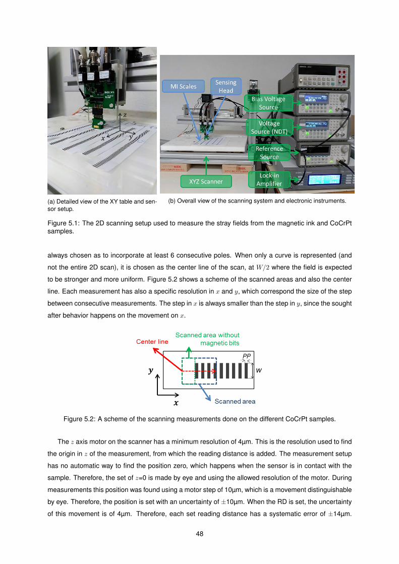
(a) Detailed view of the XY table and sen-sor setup.
(b) Overall view of the scanning system and electronic instruments.
Figure 5.1: The 2D scanning setup used to measure the stray fields from the magnetic ink and CoCrPtsamples.
always chosen as to incorporate at least 6 consecutive poles. When only a curve is represented (and
not the entire 2D scan), it is chosen as the center line of the scan, at W/2 where the field is expected
to be stronger and more uniform. Figure 5.2 shows a scheme of the scanned areas and also the center
line. Each measurement has also a specific resolution in x and y, which correspond the size of the step
between consecutive measurements. The step in x is always smaller than the step in y, since the sought
after behavior happens on the movement on x.
Figure 5.2: A scheme of the scanning measurements done on the different CoCrPt samples.
The z axis motor on the scanner has a minimum resolution of 4µm. This is the resolution used to find
the origin in z of the measurement, from which the reading distance is added. The measurement setup
has no automatic way to find the position zero, which happens when the sensor is in contact with the
sample. Therefore, the set of z=0 is made by eye and using the allowed resolution of the motor. During
measurements this position was found using a motor step of 10µm, which is a movement distinguishable
by eye. Therefore, the position is set with an uncertainty of ±10µm. When the RD is set, the uncertainty
of this movement is of 4µm. Therefore, each set reading distance has a systematic error of ±14µm.
48

Which is accounted for in the analysis of the performed measurements.
The data taken from the setup is of the voltage output of the sensor. In this stage of the work, we
are interested in evaluating the field created by the structures and also the capability of the sensors
to measure that field. Therefore, the voltage information is converted into field using the magnetic
properties from the sensors taken from the transfer curves in chapter 3 and the bias current fed to the
sensor. With these parameters, the conversion is simply done using the following equation:
H = V − VoffRS0Ib
, (5.1)
where H is the magnetic field magnitude in mT, V the output voltage from the sensor in V, Voff the offset
voltage of the measurement in V, Rmin the minimum resistance in Ω, S0 the sensitivity of the sensor in
%/mT and Ib the bias current fed to the sensor in A.
5.2 Measurements on Magnetic Ink Samples
All measurements of the magnetic ink samples are confidential and presented in Appendix ??.
Measurements on MI samples with sensor S1 using both Std 1 and Std 3 allowed the evaluation
of the best solution for the system. The use of Std 3 resulted in a higher effective magnetization of
the ink during measurements, which was already expected with the simulations of section 3.1.3, due to
the presence of the x component of the field in the region right below where the sensor is measuring.
Using both configurations resulted also in similar spatial-resolutions, since the same sensor was used.
However, the higher magnetization of the ink yields higher magnetic signal, thus more distinguishable
measuremets using Std 3.
Sensor S2, which has a greater spatial resolution than sensor S1, was tested on the same samples
and doing the same studies as with sensor S1. Sensor S2 resulted in higher spatial resolution, allowing
the measurement of smaller structures. It measures also higher magnetic signals from the samples,
due to its lower effective reading distance. However, this sensor has a lower SNR, resulting in worst
performance reading smaller magnetic signals.
5.3 Sensor Validation with CoCrPt Samples
The simulation of the CoCrPt samples using the model described in chapter 4 is done and compared
with measurements. This is done using both sensors S1 and S2 considered for this work, mounted in a
configuration Std 3, which has been proven to be the most advantageous in the previous section. This
configuration magnetizes in a more effective way the ink. It was seen however that the field created by
the magnets is not strong enough too change significantly the magnetization of the structures, therefore,
in simulations the values used for the magnetization is the remanent magnetization MR derived from the
plot on Figure 4.3. The sensitivities for both sensors in Std 3 configuration were measured in chapter 3,
yielding 14.3 %/mT for a Rmin =542 Ω for sensor S1, and -24.4 %/mT for a Rmin =1161Ω for sensor
49
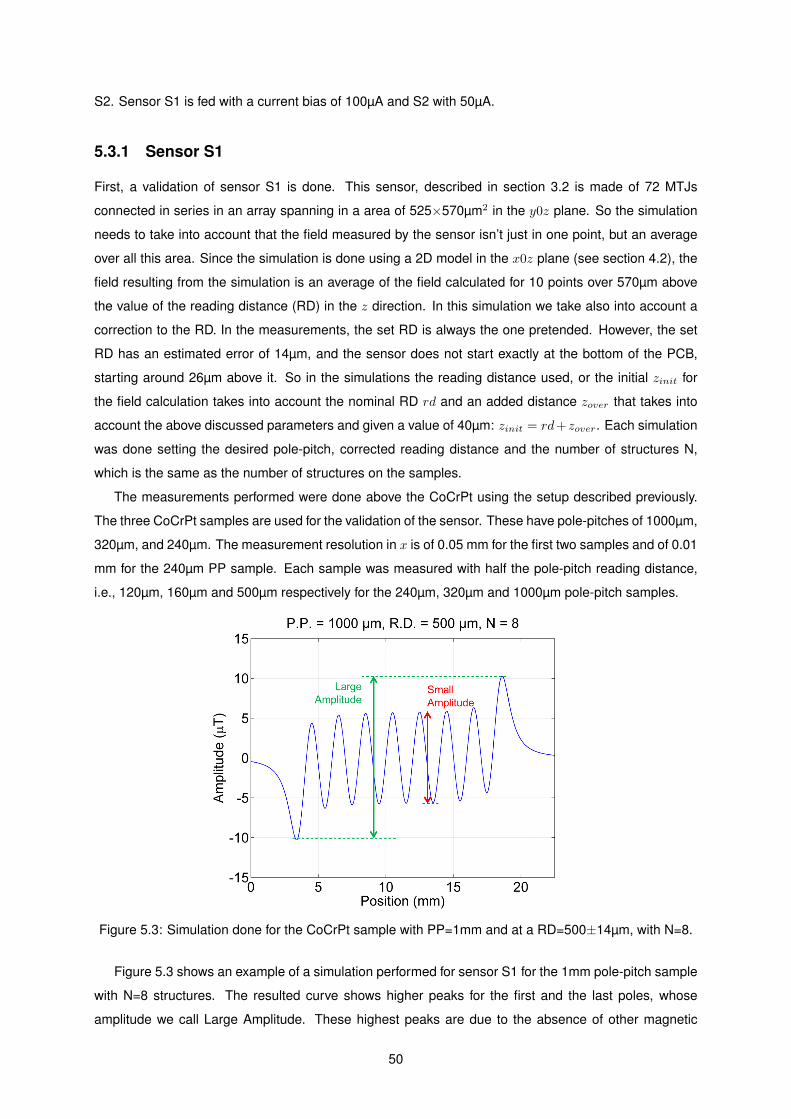
S2. Sensor S1 is fed with a current bias of 100µA and S2 with 50µA.
5.3.1 Sensor S1
First, a validation of sensor S1 is done. This sensor, described in section 3.2 is made of 72 MTJs
connected in series in an array spanning in a area of 525×570µm2 in the y0z plane. So the simulation
needs to take into account that the field measured by the sensor isn’t just in one point, but an average
over all this area. Since the simulation is done using a 2D model in the x0z plane (see section 4.2), the
field resulting from the simulation is an average of the field calculated for 10 points over 570µm above
the value of the reading distance (RD) in the z direction. In this simulation we take also into account a
correction to the RD. In the measurements, the set RD is always the one pretended. However, the set
RD has an estimated error of 14µm, and the sensor does not start exactly at the bottom of the PCB,
starting around 26µm above it. So in the simulations the reading distance used, or the initial zinit for
the field calculation takes into account the nominal RD rd and an added distance zover that takes into
account the above discussed parameters and given a value of 40µm: zinit = rd+ zover. Each simulation
was done setting the desired pole-pitch, corrected reading distance and the number of structures N,
which is the same as the number of structures on the samples.
The measurements performed were done above the CoCrPt using the setup described previously.
The three CoCrPt samples are used for the validation of the sensor. These have pole-pitches of 1000µm,
320µm, and 240µm. The measurement resolution in x is of 0.05 mm for the first two samples and of 0.01
mm for the 240µm PP sample. Each sample was measured with half the pole-pitch reading distance,
i.e., 120µm, 160µm and 500µm respectively for the 240µm, 320µm and 1000µm pole-pitch samples.
Figure 5.3: Simulation done for the CoCrPt sample with PP=1mm and at a RD=500±14µm, with N=8.
Figure 5.3 shows an example of a simulation performed for sensor S1 for the 1mm pole-pitch sample
with N=8 structures. The resulted curve shows higher peaks for the first and the last poles, whose
amplitude we call Large Amplitude. These highest peaks are due to the absence of other magnetic
50
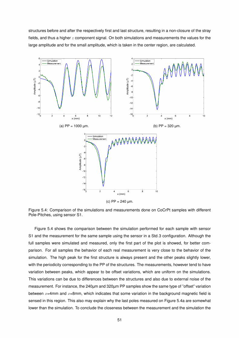
structures before and after the respectively first and last structure, resulting in a non-closure of the stray
fields, and thus a higher z component signal. On both simulations and measurements the values for the
large amplitude and for the small amplitude, which is taken in the center region, are calculated.
(a) PP = 1000 µm. (b) PP = 320 µm.
(c) PP = 240 µm.
Figure 5.4: Comparison of the simulations and measurements done on CoCrPt samples with differentPole-Pitches, using sensor S1.
Figure 5.4 shows the comparison between the simulation performed for each sample with sensor
S1 and the measurement for the same sample using the sensor in a Std 3 configuration. Although the
full samples were simulated and measured, only the first part of the plot is showed, for better com-
parison. For all samples the behavior of each real measurement is very close to the behavior of the
simulation. The high peak for the first structure is always present and the other peaks slightly lower,
with the periodicity corresponding to the PP of the structures. The measurements, however tend to have
variation between peaks, which appear to be offset variations, which are uniform on the simulations.
This variations can be due to differences between the structures and also due to external noise of the
measurement. For instance, the 240µm and 320µm PP samples show the same type of ”offset” variation
between x=4mm and x=8mm, which indicates that some variation in the background magnetic field is
sensed in this region. This also may explain why the last poles measured on Figure 5.4a are somewhat
lower than the simulation. To conclude the closeness between the measurement and the simulation the
51

two amplitudes (the large and the small) are calculated. Calculating these amplitudes along the sample
eliminates the difference that comes from the background measurement.
The plot on Figure 5.5 shows the comparison between simulation and measurements. Overall the
tendency of the measured amplitudes corresponds to the predicted by the simulations, although neither
the values nor the error bars make it a complete match. The large amplitude increases for smaller pole-
pitch structures since we are putting the sensor gradually closer to the sample as the PP decreases,
the small amplitude on the other end tends to decrease, this is due to the fact that the poles are getting
closer together, closing the stray field force lines at a closer scale resulting in a gradually weaker z
component of the field.
Figure 5.5: Average amplitudes measured both in the measurements and simulations for sensor S1 foreach sample at a RD of half the PP.
The fact that the amplitudes don’t match may come from different factors. First, an underestimation of
the uncertainty in the RD of the measurements. 14 µm was considered as the uncertainty, however, this
values may be higher, and if so, the difference between simulation and measurement could be explained.
On the other hand, the model for the simulation is a 2D approximation, where an average is performed
over the span of the sensor. This approximation may, however be faulty, and is not considering the full
extent of the field variation along the sensor. Other factor may come from the model itself, since we are
considering perfect magnetization uniformity within the material.
Nevertheless, It is safe to say that measurements done with sensor S1 are reliable. The measured
signal is very close to the predicted, and therefore one can say that the signal measured on the magnetic
ink samples with this sensor are correct and can be taken as a reference for future measurements.
5.3.2 Sensor S2
For sensor S2 the simulation simplifies since the sensing region in the x0z plane is much smaller, being
of just 4µm. Therefore, the field calculated in the simulation for this sensor is done on just one point at
52
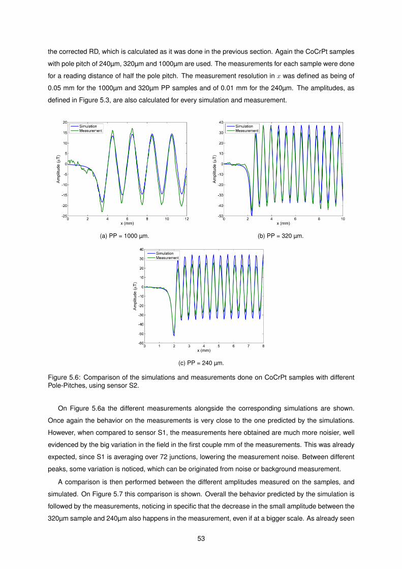
the corrected RD, which is calculated as it was done in the previous section. Again the CoCrPt samples
with pole pitch of 240µm, 320µm and 1000µm are used. The measurements for each sample were done
for a reading distance of half the pole pitch. The measurement resolution in x was defined as being of
0.05 mm for the 1000µm and 320µm PP samples and of 0.01 mm for the 240µm. The amplitudes, as
defined in Figure 5.3, are also calculated for every simulation and measurement.
(a) PP = 1000 µm. (b) PP = 320 µm.
(c) PP = 240 µm.
Figure 5.6: Comparison of the simulations and measurements done on CoCrPt samples with differentPole-Pitches, using sensor S2.
On Figure 5.6a the different measurements alongside the corresponding simulations are shown.
Once again the behavior on the measurements is very close to the one predicted by the simulations.
However, when compared to sensor S1, the measurements here obtained are much more noisier, well
evidenced by the big variation in the field in the first couple mm of the measurements. This was already
expected, since S1 is averaging over 72 junctions, lowering the measurement noise. Between different
peaks, some variation is noticed, which can be originated from noise or background measurement.
A comparison is then performed between the different amplitudes measured on the samples, and
simulated. On Figure 5.7 this comparison is shown. Overall the behavior predicted by the simulation is
followed by the measurements, noticing in specific that the decrease in the small amplitude between the
320µm sample and 240µm also happens in the measurement, even if at a bigger scale. As already seen
53

for sensor S1, the increase of the large amplitude as the pole-pitch decreases has to do with getting
gradually closer to the sample. However, the predicted behavior for the small amplitude is different from
the predicted behavior for sensor S1. It must be present here that sensor S1 is averaging over an area
that spans 570µm over z, this results in an effective reading distance of the half pole-pitch plus around
200µm which is of 700µm for 1000µm PP, 360µm for 320µm PP and so on. While 200µm is just a
relatively small fraction of 1000µm, it makes already a big portion of 320µm adn 240µm. Therefore, with
sensor S2 the sensor is significantly closer to the sample, and so, the magnetic field from the smaller
pole pitches is higher than for 1000µm sample. Then, comparing the lower PP sizes, the explanation
given for sensor S1 holds, since the structures are much closer to each other, the stray field closes in a
smaller scale, decreasing the signal.
Figure 5.7: Amplitudes measured both in the measurements and simulations for sensor S2 for eachsample at a RD of half the PP.
Sensor S2, even though having a lower SNR, in a Std 3 configuration its sensitivity and spatial
resolution are higher than for sensor S1. Resulting in a much better expected performance in terms of
resolution for this sensor. This comes as a great advantage for reading magnetic ink. The closeness
of the measurements to the simulations validates also this sensor, and the procedure used, making it a
reliable sensor for reliable measurements.
54

Chapter 6
Conclusions
The aim of this work has been to develop a reading head based on the TMR sensor technology for
reading magnetic ink patterns, in particular for positioning application. This system should be able to
magnetize the ink as well as measure it with high accuracy and sensitivity.
As a first stage, the strategy for magnetizing the ink was developed. From the multiple choices to
create a field in the track region, the implementation of magnets alongside the sensor was chosen,
due to its simplicity and non-requirement for further electronics. The configuration of the magnets in
relation to the sensor had to be carefully thought, taking into account the desired direction for the ink
magnetization (x) and other specifications of the project. Resulting in the placement of two magnets
at the same distance from the sensor, which is placed halfway between them. The simple simulations
performed for the configurations resulted on a reliable prediction on the efficiency of magnetization of
the magnetic ink, as well as providing a good prediction on the influence on the TMR sensors mounted
on the system. The two resulting configurations differ in the direction of magnetization of the magnets
and on the relative position of the sensor (Std 1 and Std 3).
The influence of these configurations on the two considered sensor configurations was tested. Sen-
sor S1, comprised of 72 MTJs in series occupying an area of 525×570 µm2 with a large SNR, a minimum
resistance of 542Ω and a sensitivity of 27.7%/mT; and sensor S2, comprised of 4 MTJS in series oc-
cupying an area of 58.5×4 µm2 with a large SNR, a minimum resistance of 1187Ω and a sensitivity of
-22.2%/mT. The influence of the first considered configuration Std 1 on sensor S1 was large, resulting in
non-consistent responses on different measurements, resulting always in a decrease on the sensitivity
due to influence of the external field on the sensitive direction of the sensor. On sensor S2, the influ-
ence of this configuration was too big, and no linear region was obtained. The influence of the second
configuration Std 3 was mainly on the sensitivity value due to the influence of cross fields in the sensor
sensitive plane. Decreasing the sensitivity of sensor S1 to 14.3%/mT and increasing the sensitivity of
S2 to -24.4%/mT by shifting the curve.
A strategy to validate the sensors was also developed, comprising on the micro-fabrication in a
clean-room environment of well-defined structures of a CoCrPt hard ferromagnetic alloy. The simulation
of this structures compared with measurements showed that the measurements for both sensors are
55

reliable, and that their response is very close to the simulations, showing the same tendency on both
sensors. Tendency apart, the values of the amplitude still didn’t exactly correspond, showing the results
of the approximations taken in the simulation performed. It was a 2D model, therefore leaving out some
3D geometrical features that would influence the signal. These measurements allowed as well a good
comparison between the two sensors used. Even though having a lower SNR, sensor S2 is capable of
measuring higher amplitudes and has a better spatial resolution than sensor S1.
Measurements performed on the Magnetic Ink samples, led to the conclusion on the best performing
configuration for this kind of system, revealing that one of the configurations, Std 3, is more efficient in
magnetizing the magnetic media upon measurement.
With this work, we were therefore able to find a configuration with a very good performance in mag-
netizing the magnetic ink, as well as validating the state-of-the-art TMR sensors for this application.
Furthermore, the foundations for a future development of the system has been set.
Future work in this project should include the optimization of the sensors for this configuration. Even
though a high spatial resolution sensor was found, the SNR is still low, requiring some future improve-
ment. The CoCrPT tracks, which proved to be a good validation tool for the sensors can also be opti-
mized by fabricating higher thicknesses of alloy and therefore measuring higher signals, making a more
versatile tool for different kind of studies.
56

Bibliography
[1] P. Freitas, R. Ferreira, S. Cardoso, and F. Cardoso. Magnetoresistive sensors. Journal of Physics:
Condensed Matter, 19(16):165221, 2007.
[2] P. P. Freitas, R. Ferreira, and S. Cardoso. Spintronic sensors. Proceedings of the IEEE, 104(10):
1894–1918, 2016.
[3] S. P. Gubin. Magnetic nanoparticles. John Wiley & Sons, 2009.
[4] BOGEN Electronic GmbH. Magnetic Measurement Technology. http://www.bogen-electronic.
com/en/magnetic-measurement-solutions/technology.html. Accessed: 2017-08-28.
[5] E. Eitel. Basics of rotary encoders: overview and new technologies. http://machinedesign.
com/sensors/basics-rotary-encoders-overview-and-new-technologies-0, 2014. Accessed:
2017-08-28.
[6] S. Tumanski. Magnetic sensors. In Handbook of magnetic measurements, pages 159–256. CRC
Press, 2016.
[7] D. Leitao, J. Borme, A. Orozco, S. Cardoso, and P. Freitas. Magnetoresistive sensors for surface
scanning. In Giant Magnetoresistance (GMR) Sensors, pages 275–299. Springer, 2013.
[8] A. Oral, S. Bending, and M. Henini. Real-time scanning hall probe microscopy. Applied physics
letters, 69(9):1324–1326, 1996.
[9] V. Mor, M. Schultz, O. Sinwani, A. Grosz, E. Paperno, and L. Klein. Planar hall effect sensors with
shape-induced effective single domain behavior. Journal of Applied Physics, 111(7):07E519, 2012.
[10] A. V. Silva, D. C. Leitao, J. Valadeiro, J. Amaral, P. P. Freitas, and S. Cardoso. Linearization strate-
gies for high sensitivity magnetoresistive sensors. The European Physical Journal Applied Physics,
72(1):10601, 2015.
[11] S. Si, C. Li, X. Wang, D. Yu, Q. Peng, and Y. Li. Magnetic monodisperse fe3o4 nanoparticles.
Crystal growth & design, 5(2):391–393, 2005.
[12] X. Zhou, C. Fang, Y. Li, N. An, and W. Lei. Preparation and characterization of fe 3 o 4-cnts
magnetic nanocomposites for potential application in functional magnetic printing ink. Composites
Part B: Engineering, 89:295–302, 2016.
57

[13] MICR Basics Handbook. TROY Group, Inc., October 2004.
[14] M. GmbH. Investigation and quality control of bank note safety features.
https://matesy.de/en/products/magnetic-field-visualization/applications/
investigation-and-quality-control-of-bank-note-safety-features. Accessed: 2017-
08-28.
[15] J. M. Coey. Magnetism and magnetic materials, chapter 2, pages 24–61. Cambridge University
Press, 2010.
[16] H. N. Bertram. Theory of magnetic recording. Cambridge University Press, 1994.
[17] J. M. Coey. Magnetism and magnetic materials. Cambridge University Press, 2010.
[18] W. D. Callister and D. G. Rethwisch. Fundamentals of materials science and engineering, volume
471660817. Wiley London, 2000.
[19] C. Bean and u. D. Livingston. Superparamagnetism. Journal of Applied Physics, 30(4):S120–S129,
1959.
[20] M. Julliere. Tunneling between ferromagnetic films. Physics letters A, 54(3):225–226, 1975.
[21] S. Yuasa and D. Djayaprawira. Giant tunnel magnetoresistance in magnetic tunnel junctions with a
crystalline mgo (0 0 1) barrier. Journal of Physics D: Applied Physics, 40(21):R337, 2007.
[22] J. S. Moodera, J. Nassar, and G. Mathon. Spin-tunneling in ferromagnetic junctions. Annual Review
of Materials Science, 29(1):381–432, 1999.
[23] J. Nogues and I. K. Schuller. Exchange bias. Journal of Magnetism and Magnetic Materials, 192
(2):203–232, 1999.
[24] R. Bai, Z. H. Qian, Y. C. Sun, J. P. Li, H. C. Zhu, L. W. Li, Y. Li, D. X. Huo, and H. L. Zhan. Effects
of different relevant layers on magnetic properties of bottom synthetic irmn spin valves. In Key
Engineering Materials, volume 562, pages 1467–1470. Trans Tech Publ, 2013.
[25] P. W. Pong and W. F. Egelhoff. Enhancement of tunneling magnetoresistance by optimization of cap-
ping layer thicknesses in cofeb/mgo/cofeb magnetic tunnel junctions. Journal of Applied Physics,
105(7):07C915, 2009.
[26] A. Guedes, M. Mendes, P. Freitas, and J. Martins. Study of synthetic ferrimagnet-synthetic anti-
ferromagnet structures for magnetic sensor application. Journal of applied physics, 99(8):08B703,
2006.
[27] M. Rickart, A. Guedes, B. Negulescu, J. Ventura, J. Sousa, P. Diaz, M. MacKenzie, J. Chapman,
and P. Freitas. Exchange coupling of bilayers and synthetic antiferromagnets pinned to mnpt. The
European Physical Journal B-Condensed Matter and Complex Systems, 45(2):207–212, 2005.
58

[28] B. Negulescu, D. Lacour, F. Montaigne, A. Gerken, J. Paul, V. Spetter, J. Marien, C. Duret, and
M. Hehn. Wide range and tunable linear magnetic tunnel junction sensor using two exchange
pinned electrodes. Applied Physics Letters, 95(11):112502, 2009.
[29] J. Zhang and R. White. Voltage dependence of magnetoresistance in spin dependent tunneling
junctions. Journal of applied physics, 83(11):6512–6514, 1998.
[30] supermagnete. Block magnets neodymium. https://www.supermagnete.pt/
block-magnets-neodymium. Accessed: 2017-10-16.
[31] F. Franco, F. A. Cardoso, L. S. Rosado, R. Ferreira, S. Cardoso, M. Piedade, and P. P. Freitas.
Advanced ndt inspection tools for titanium surfaces based on high-performance magnetoresistive
sensors. IEEE Transactions on Magnetics, 53(4):1–5, 2017.
[32] F. A. Cardoso, L. S. Rosado, F. Franco, R. Ferreira, E. Paz, S. F. Cardoso, P. M. Ramos, M. Piedade,
and P. J. Freitas. Improved magnetic tunnel junctions design for the detection of superficial defects
by eddy currents testing. IEEE Transactions on Magnetics, 50(11):1–4, 2014.
[33] M. A. Lieberman and A. J. Lichtenberg. Principles of plasma discharges and materials processing.
John Wiley & Sons, 2005.
[34] R. Sousa. Magnetic Random Access Memory (MRAM) based on Spin Dependent Tunnel Junctions.
PhD thesis, Instituto Superior Tecnico, 2002.
[35] J. P. D. Valadeiro. Magnetoresistive sensors with pico-tesla sensitivities. Master’s thesis, Instituto
Superior Tecnico, September 2014.
59

60

Appendix A
CoCrPt Structures Micro-Fabrication
Process Runsheet
Runsheet of the micro-fabrication process of the CoCrPt structures described in section 4.1.
A.1

Run Sheet – GePos |Magnetic Scales
Responsible: Tiago Costa Process Start: 24 / 07 / 2017 Process Finish: ____ / ____ / _______
STEP 1: CoCrPt (1000 Å) Deposition 24-25/07/2017
Machine: Alcatel SCM450 – Radio Frequency (RF) Sputtering Deposition Operator: Tiago Monteiro
Tiago Costa
Sample (2 phases):
1. Calibration sample: 1 glass substrate (25x25mm2)
2. Working samples: 3x glass substrates (25x25 mm) + silicon substrate for composition test
Material: Co66Cr16Pt18 Thickness: 1000Å
Conditions:
1. Calibration Sample
Base Pressure: 1.62x10⁻⁶ Torr, RF Power: 40 W, Ar flux: 20 sccm, Vbias : 820 V
Chamber Pressure: 2.14 mTorr, Deposition rate: 6.48 Å/min, Total time: 154 min
2. Working samples + silicon substrate
Base Pressure: 3.60x10⁻⁶ Torr, RF Power: 40 W, Ar flux: 20 sccm, Vbias :800 V
Chamber Pressure: 2.12 mTorr, Deposition rate: 6.48 Å/min, Total time: 154 min
Observations
Glass Substrates cleaned : Alconox + Ultrasounds / DI water rinse / Dry with compressed air gun
Silicon substrate cleaned: Acetone / DI water rinse / Dry with compressed air gun
For calibration sample, vacuum done from Friday 21/07 to Monday 24/07. (~55h)
Before calibration sample, target was cleaned for 3hours:
o 40WRF/20sccm/800Vbias/2.10mTorr/3h
For working samples, vacuum done from Monday 24/07 to Tuesday 25/07. (~20h)
Before working sample, target was cleaned for 1hour:
o 40WRF/20sccm/800Vbias/2.09mTorr/1h
Analysis :
1. Profilometer with calibration sample (all in Å) – Dekdak Operator: Tiago Costa
Scan length: 300μm / Speed: Low / Resolution: High. Av. High and Av. Low taken from the program.
1 2 3 4 5 6 7 8 9 10 11 12 13
Av. Low -69 178 86 2 64 80 161 119 160 -244 158 -5 87
Av. High 1110 1128 1031 956 1128 1179 887 1149 1134 990 1103 1087 1042 Overall Av.
Av. Thick. 1179 950 945 954 1064 1099 726 1030 974 1234 945 1092 955 1011±123
CoCrPt (1000 Å)
Glass Substrate
STEP 2: Lithography – Magnetic Poles definition /2xsamples 16-18/ 08 /2017
Machine: DWL - Direct Write Laser Litography (diode laser) Operator: Karla / Tiago Costa
1. Sample no. 1 – Full Scales
1.1 Vapor Prime 30 min (Recipe – 0)
(25 min N2 atmosphere + 5 min HDMS) at 130ºC and P=5Torr
1.2 Coat 1.5 µm Photoresit (Recipe 6/2)
Photoresist
Spinning for 40s at 2500 rpm (1.5 µm thickness);
Baking for 60s at 100ºC 1.3 Lithography (Single Exposure)
Map: AMSION Mask: cocrpt_scales_full_INV (INVERTED)
Energy: 55 Focus: 0
Die dimensions: [X: 19400; Y: 19400] m
# Dies: 1 Total Time:
[X0: 3000Y0: 3000 ] m (From bottom left corner)
1.4 Development (Recipe 6/2)
Time: 3min 10s
Sample heating: 60s at 110ºC; Cool down: 30s; Developing: 100s
2. Sample no. 2 – VSM and Profile Test structures
2.1. Vapor Prime 30 min (Recipe – 0)
(25 min N2 atmosphere + 5 min HDMS) at 130ºC and P=5Torr
2.2. Coat 1.5 µm Photoresit (Recipe 6/2)
Photoresist
Spinning for 40s at 2500 rpm (1.5 µm thickness);
Baking for 60s at 100ºC
2.3. Lithography (Single Exposure)
Map: AMSION Mask: cocrpt_scales_tests_INV (INVERTED)
Energy: 55 Focus: 0
Die dimensions: [X: 19400; Y: 19400] m
# Dies: 1 Total Time:
[X0: 3000Y0: 3000 ] m (From bottom left corner)
2.4. Development (Recipe 6/2)
Time: 3min 10s
Sample heating: 60s at 110ºC; Cool down: 30s; Developing: 100s
Observations:
Lithography performed 1.5 days after photo-resist coating.
Scheme :
Resist Coating : After Development ;
(x0,y0)
25.4mm
25.4mm
CoCrPt (1000 Å)
Glass Substrate
Photoresist

Sampe no. 1 AutoCAD mask:
o Pole-pitch (width of the stripes) from bottom to top (m): 80, 160, 240, 320, 1000.
o All scales have same length (3mm)
Optical Inspection
The sizes of the structures are good. The borders are also well defined. Apart from some non-uniformity on the PR
due to scratches observed on the surface of the metal, there is nothing else to account for Some pictures were
taken:
~
19.4mm
19.4mm 3mm 3.88mm
Marks for
dicing
200μm 200μm
200μm 200μm 200μm
200μm
200μm
200μm 200μm
STEP 3: CoCrPt etching by Ion Milling 19/08/2017
Machine: Nordiko 3000 Operator: Karla
Total thickness to etch: 1000 Å (etch rate: 0.8 Å/s); time: 1250 sec @ 70º
Base Pressure (Torr): 7.8x10⁻⁷ Torr Batch: Junction Etch
Recipe: Etch Junction Pillar 4
Steps: Vacuum wait / etch gun stab 70º pan / junction etch 70º pan / end etch
Observations:
After Etching:
Optical inspection :
It is visible that the etch is done completely. Borders are well defined. Just some sparse residues of metal where it
should have been etched.
Note: No pictures were taken after this step.
STEP 4: Resist Strip at Wet Bench 19/08/2017
Operator: Karla
Conditions: Microstrip + Temperature: 60ºC + Ultrasounds
Cleaning: IPA rinse / DI water rinse / Dry with compressed air gun
Observations:
Optical Inspection: 24/08/2017
Overall the structures are well defined and almost no anomalies on the structures.
Some pictures were taken: On the second, seventh and eigth pictures one can see the pieces of metal that were not
etched. Apart from these ones, no others were evidenced. On the eighth picture the anomalies appear to be due to
scratches on the substrates.
Assist Gun Power (W) V+ (V) I+ (mA) V- (V) I- (mA) Ar Flux (sccm) Pan (deg) Rotation (rpm)
Read Values 53 488.3 28.7 194.3 1.7 7.9 70 40
CoCrPt (1000 Å)
Glass Substrate
Photoresist
CoCrPt (1000 Å)
Glass Substrate
STEP 5: Annealing 25/08/2017
Machine: Old Annealing Setup Operator: Tiago Costa
Conditions:
Observations : A current I=182000ppm to the Helmoltz Coils is applied.
Note : Tset = 375 ºC --> Treal = 350 ºC
Heating Rate = 5.9 ºC/min
200μm 200μm
200μm 200μm
200μm
200μm
200μm 200μm
60 min
22.4
2 h
22.4
375
2 h
22.4
0.5 T
2 h
22.4
Applied Field


![Uppsala University - DiVA portaluu.diva-portal.org/smash/get/diva2:576768/FULLTEXT02.pdfmemory circuits [19]. Other disadvantages with magnetoresistive sensors are their relatively](https://img.pdfslide.us/doc/110x75/60ffeb8cca0125006e0919b4/uppsala-university-diva-576768fulltext02pdf-memory-circuits-19-other-disadvantages.jpg)