Embed Size (px)
Citation preview

October 2015 DocID024675 Rev 3 1/40
AN4300Application note
Advanced light control and diagnostics usingSPC56xBx/RPC56xBx and SPC56xCx microcontrollers
IntroductionThe members of the SPC56xBx/RPC56xBx and SPC56xCx families are high performance microcontrollers developed for car body application needs. These devices are especially useful in automotive light management applications and offer features to assist the car body system developer in writing optimized firmware with a very low CPU load.
This document offers an interesting example about the interconnection between the eMIOS, CTU, and ADC modules of the SPC56EC74 (one member of the SPC56xB/RPC56xBx/Cx family) in a lighting application, including the support of circuitry diagnostics, without placing an additional load on the MCU’s CPU. This example is easily applied to each device of the SPC56xB/RPC56xBx/Cx family.
www.st.com
Contents AN4300
2/40 DocID024675 Rev 3
Contents
1 Lighting application design challenge . . . . . . . . . . . . . . . . . . . . . . . . . . 61.1 General light application aspects . . . . . . . . . . . . . . . . . . . . . . . . . . . . . . . . 6
1.2 Driver signals characteristics . . . . . . . . . . . . . . . . . . . . . . . . . . . . . . . . . . . 7
1.3 System proposal . . . . . . . . . . . . . . . . . . . . . . . . . . . . . . . . . . . . . . . . . . . . . 7
1.4 Diagnosis check . . . . . . . . . . . . . . . . . . . . . . . . . . . . . . . . . . . . . . . . . . . . . 81.4.1 Digital diagnosis . . . . . . . . . . . . . . . . . . . . . . . . . . . . . . . . . . . . . . . . . . . . 9
1.4.2 Analog diagnosis . . . . . . . . . . . . . . . . . . . . . . . . . . . . . . . . . . . . . . . . . . . 9
1.4.3 Serial diagnosis . . . . . . . . . . . . . . . . . . . . . . . . . . . . . . . . . . . . . . . . . . . . 9
2 SPC56xBx/RPC56xBx features to cover lighting needs . . . . . . . . . . . 112.1 eMIOS (enhanced Modular Input/Output Subsystem) . . . . . . . . . . . . . . . 11
2.2 CTU (Cross Triggering Unit) . . . . . . . . . . . . . . . . . . . . . . . . . . . . . . . . . . . 12
2.3 ADC (Analog-to-Digital Converter) . . . . . . . . . . . . . . . . . . . . . . . . . . . . . . 13
3 Lighting application example architecture . . . . . . . . . . . . . . . . . . . . . . 143.1 Hardware architecture . . . . . . . . . . . . . . . . . . . . . . . . . . . . . . . . . . . . . . . 15
3.1.1 Generalities on M0-6 . . . . . . . . . . . . . . . . . . . . . . . . . . . . . . . . . . . . . . . 15
3.2 Software Implementation . . . . . . . . . . . . . . . . . . . . . . . . . . . . . . . . . . . . . 163.2.1 Synchronous diagnosis . . . . . . . . . . . . . . . . . . . . . . . . . . . . . . . . . . . . . 16
3.3 Synchronous Analog Diagnosis . . . . . . . . . . . . . . . . . . . . . . . . . . . . . . . . 18
3.4 Implementation of the synchronous diagnosis . . . . . . . . . . . . . . . . . . . . . 19
4 MCU initialization . . . . . . . . . . . . . . . . . . . . . . . . . . . . . . . . . . . . . . . . . . 204.1 Setting up Mode Entry and clocks . . . . . . . . . . . . . . . . . . . . . . . . . . . . . . 20
4.2 DSPI configuration . . . . . . . . . . . . . . . . . . . . . . . . . . . . . . . . . . . . . . . . . . 21
4.3 eMIOS_0 and EMIOS_1 modules . . . . . . . . . . . . . . . . . . . . . . . . . . . . . . 224.3.1 eMIOS_0 and eMIOS_1 module initialization . . . . . . . . . . . . . . . . . . . . 22
4.4 DMA module . . . . . . . . . . . . . . . . . . . . . . . . . . . . . . . . . . . . . . . . . . . . . . . 27
4.5 ADC module . . . . . . . . . . . . . . . . . . . . . . . . . . . . . . . . . . . . . . . . . . . . . . . 314.5.1 Check Voltage Battery function . . . . . . . . . . . . . . . . . . . . . . . . . . . . . . . 33
4.6 CTU module . . . . . . . . . . . . . . . . . . . . . . . . . . . . . . . . . . . . . . . . . . . . . . . 35
4.7 Micro Resources summary . . . . . . . . . . . . . . . . . . . . . . . . . . . . . . . . . . . . 36

DocID024675 Rev 3 3/40
AN4300 Contents
3
5 Conclusion . . . . . . . . . . . . . . . . . . . . . . . . . . . . . . . . . . . . . . . . . . . . . . . . 37
Appendix A Reference documents . . . . . . . . . . . . . . . . . . . . . . . . . . . . . . . . . . . . 38A.1 Reference documents . . . . . . . . . . . . . . . . . . . . . . . . . . . . . . . . . . . . . . . . 38
A.2 Acronyms. . . . . . . . . . . . . . . . . . . . . . . . . . . . . . . . . . . . . . . . . . . . . . . . . . 38
Revision history . . . . . . . . . . . . . . . . . . . . . . . . . . . . . . . . . . . . . . . . . . . . . . . . . . . . 39

List of tables AN4300
4/40 DocID024675 Rev 3
List of tables
Table 1. Resources allocated on the microcontroller . . . . . . . . . . . . . . . . . . . . . . . . . . . . . . . . . . . . 36Table 2. Acronyms . . . . . . . . . . . . . . . . . . . . . . . . . . . . . . . . . . . . . . . . . . . . . . . . . . . . . . . . . . . . . . 38Table 3. Document revision history. . . . . . . . . . . . . . . . . . . . . . . . . . . . . . . . . . . . . . . . . . . . . . . . . . 39
DocID024675 Rev 3 5/40
AN4300 List of figures
5
List of figures
Figure 1. Lamp light bulb characteristics . . . . . . . . . . . . . . . . . . . . . . . . . . . . . . . . . . . . . . . . . . . . . . . 6Figure 2. System solution for light application . . . . . . . . . . . . . . . . . . . . . . . . . . . . . . . . . . . . . . . . . . . 8Figure 3. Light management . . . . . . . . . . . . . . . . . . . . . . . . . . . . . . . . . . . . . . . . . . . . . . . . . . . . . . . 10Figure 4. eMIOS, ADC and CTU interconnection scheme. . . . . . . . . . . . . . . . . . . . . . . . . . . . . . . . . 11Figure 5. eMIOS-OPWMT mode . . . . . . . . . . . . . . . . . . . . . . . . . . . . . . . . . . . . . . . . . . . . . . . . . . . . 12Figure 6. Lighting application—example system concept . . . . . . . . . . . . . . . . . . . . . . . . . . . . . . . . . 14Figure 7. SPC56EC74L7 Minimodule + M0-6 Board . . . . . . . . . . . . . . . . . . . . . . . . . . . . . . . . . . . . . 15Figure 8. Initial Configuration flowchart . . . . . . . . . . . . . . . . . . . . . . . . . . . . . . . . . . . . . . . . . . . . . . . 17Figure 9. Vbat measurement and duty-cycle update flowchart . . . . . . . . . . . . . . . . . . . . . . . . . . . . . 18Figure 10. Delay between the CS_Sync and Output channel/Current Sense signal . . . . . . . . . . . . . . 19Figure 11. MC_Mode_Init function7. . . . . . . . . . . . . . . . . . . . . . . . . . . . . . . . . . . . . . . . . . . . . . . . . . . 20Figure 12. PLL initialization function . . . . . . . . . . . . . . . . . . . . . . . . . . . . . . . . . . . . . . . . . . . . . . . . . . 21Figure 13. DSPI master init function . . . . . . . . . . . . . . . . . . . . . . . . . . . . . . . . . . . . . . . . . . . . . . . . . . 22Figure 14. eMIOS init function . . . . . . . . . . . . . . . . . . . . . . . . . . . . . . . . . . . . . . . . . . . . . . . . . . . . . . . 23Figure 15. eMIOS clock init function . . . . . . . . . . . . . . . . . . . . . . . . . . . . . . . . . . . . . . . . . . . . . . . . . . 23Figure 16. eMIOS_0 configuration code . . . . . . . . . . . . . . . . . . . . . . . . . . . . . . . . . . . . . . . . . . . . . . . 24Figure 17. eMIOS_1 Ch23 and Ch0 configuration code . . . . . . . . . . . . . . . . . . . . . . . . . . . . . . . . . . . 25Figure 18. eMIOS_1 Ch1 and Ch2 configuration code . . . . . . . . . . . . . . . . . . . . . . . . . . . . . . . . . . . . 25Figure 19. eMIOS_1 Ch25, Ch26 and Ch 17 configuration code. . . . . . . . . . . . . . . . . . . . . . . . . . . . . 26Figure 20. eMIOS_1 Ch18 configuration code. . . . . . . . . . . . . . . . . . . . . . . . . . . . . . . . . . . . . . . . . . . 26Figure 21. Init DMA Vbat function . . . . . . . . . . . . . . . . . . . . . . . . . . . . . . . . . . . . . . . . . . . . . . . . . . . . 27Figure 22. SPI_Vbat_SetTCD function . . . . . . . . . . . . . . . . . . . . . . . . . . . . . . . . . . . . . . . . . . . . . . . . 28Figure 23. initDMA_1 function part 1 . . . . . . . . . . . . . . . . . . . . . . . . . . . . . . . . . . . . . . . . . . . . . . . . . . 29Figure 24. initDMA_1 function part 2 . . . . . . . . . . . . . . . . . . . . . . . . . . . . . . . . . . . . . . . . . . . . . . . . . . 30Figure 25. init DMA_1 function part 3. . . . . . . . . . . . . . . . . . . . . . . . . . . . . . . . . . . . . . . . . . . . . . . . . . 31Figure 26. ADC init function . . . . . . . . . . . . . . . . . . . . . . . . . . . . . . . . . . . . . . . . . . . . . . . . . . . . . . . . . 32Figure 27. ADC_0 CH0 EoC interrupt service routine . . . . . . . . . . . . . . . . . . . . . . . . . . . . . . . . . . . . . 33Figure 28. Check Voltage Battery function part1 . . . . . . . . . . . . . . . . . . . . . . . . . . . . . . . . . . . . . . . . . 34Figure 29. Check Voltage Battery function part2 . . . . . . . . . . . . . . . . . . . . . . . . . . . . . . . . . . . . . . . . . 35Figure 30. bctu_init function. . . . . . . . . . . . . . . . . . . . . . . . . . . . . . . . . . . . . . . . . . . . . . . . . . . . . . . . . 36
Lighting application design challenge AN4300
6/40 DocID024675 Rev 3
1 Lighting application design challenge
1.1 General light application aspectsIn an automotive lighting application it is necessary to drive two types of lights:1. Bulb lamp2. LED
When controlling the lamp light bulb, two points must be addressed: Lamp power supply variations Lamp lifetime
Lamp power supply voltage may differ when compared to its nominal value. Figure 1 displays how lamp lifetime depends on power supply voltage. The impact of 5 % overvoltage (630 mV at 12.6 V) on light bulb performance is significant, as indicated by the vertical line in the figure. The light bulb luminous flux grows up to 120 % and the light bulb lifetime is reduced to less than 60 %, when compared to nominal values. Therefore, the lamp power supply voltage should be regulated to the nominal value to maintain lamp lifetime. The most common control technique is the PWM, which can also be used for lamp light beam intensity control.
Figure 1. Lamp light bulb characteristics
A lamp’s lifetime is limited and it can be shortened if the lamp is connected in a faulty environment. If the design includes lamp diagnostics and protection, the lamp’s nominal lifetime can be preserved. Usually the load drivers report various diagnosis information and the light application has to collect and check this information. These factors must taken into account when designing a lighting module.
DocID024675 Rev 3 7/40
AN4300 Lighting application design challenge
39
1.2 Driver signals characteristicsThe signals that drive the light loads must satisfy the following requirements: Capability to drive up to 60 channels with PWM signals Capability to drive different load types using PWM signals with different characteristics:
– Bulb lampPWM frequency: ~100 HzDuty cycle: 50 to 100 %Duty cycle adjustment precision: usually 5 %
– LEDPWM frequency: 150 to 200 HzDuty cycle: 10 % to 100 % (as much as 2 % to 100 % for high efficiency LED)Duty cycle adjustment precision: usually 1–2 %
The variation of the duty cycle is performed to maintain constant power on the lamps when the battery voltage changes.
The duty cycle variation is based on the following expression:
Equation 1
whereVref is the nominal value of the battery voltageVbat is the actual battery voltage
If Vbat ≤ Vref, the duty cycle is equal to 100 %, else the expression is applied. The adaptation of the duty cycle is performed one time per period.
A typical battery voltage value for automotive applications is 13.2 V, so if, for example, the application reads a Vbat equal to 16 V, a duty cycle of 68 % applies.
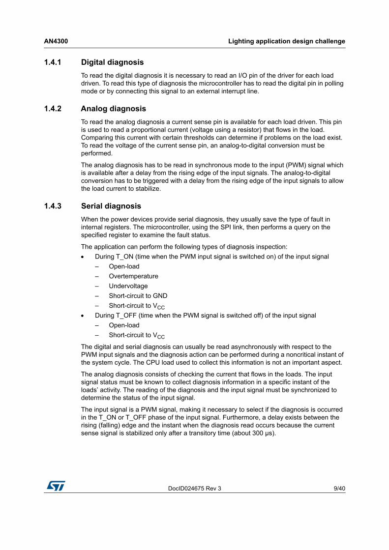
When turning the lamp light bulb on, the bulb current applied to a cold filament can reach up to 10 times the rated current. The total current of several lamps causes a significant power supply voltage drop and an increase in the electromagnetic interference (or EMI) emissions. Therefore, it is essential not to drive all lamps together and it is necessary to introduce a delay between each pair of rising edges of the PWM signals (see Figure 3).
1.3 System proposalIn a typical system solution for a light application, the SPC56xB/SPC56xCx/RPC56xB microcontroller family can manage several power drivers, depending on how the power is managed and the number of channels to be driven.
Some devices are driven by an SPI link. Using this link, the application can configure the signals, that are generated inside the driver device, to drive the loads.
Lighting application design challenge AN4300
8/40 DocID024675 Rev 3
Other devices need an input signal (PWM signals) for each load to generate the output signal to drive the loads.
It is possible to use both the microcontroller and the power devices for the solution shown in Figure 2. This solution is configured with an STMicroelectronics power driver and the SPC56EC74 microcontroller.
Figure 2. System solution for light application
This system uses devices that are driven by PWM input signals and other devices that use an SPI connection to configure the drivers.
1.4 Diagnosis checkToday’s requests for automotive systems are based not only upon technical features and reliability, but also upon increasingly important safety concepts. To fulfill these requirements, a system must provide and communicate feedback on its behavior to external devices. This, in turn, makes it possible to detect faults and react to them in a specified time.
The power drivers used in light applications provide diagnostic signals that give information about the status of loads driven. These signals must be read and interpreted to give feedback to the application. It is important to understand if there are faults and to execute protective action to obtain a safe and robust system.
Three different diagnosis types exist: Digital Analog Serial
The diagnosis types are explained in the following sections.
DocID024675 Rev 3 9/40
AN4300 Lighting application design challenge
39
1.4.1 Digital diagnosisTo read the digital diagnosis it is necessary to read an I/O pin of the driver for each load driven. To read this type of diagnosis the microcontroller has to read the digital pin in polling mode or by connecting this signal to an external interrupt line.
1.4.2 Analog diagnosisTo read the analog diagnosis a current sense pin is available for each load driven. This pin is used to read a proportional current (voltage using a resistor) that flows in the load. Comparing this current with certain thresholds can determine if problems on the load exist. To read the voltage of the current sense pin, an analog-to-digital conversion must be performed.
The analog diagnosis has to be read in synchronous mode to the input (PWM) signal which is available after a delay from the rising edge of the input signals. The analog-to-digital conversion has to be triggered with a delay from the rising edge of the input signals to allow the load current to stabilize.
1.4.3 Serial diagnosisWhen the power devices provide serial diagnosis, they usually save the type of fault in internal registers. The microcontroller, using the SPI link, then performs a query on the specified register to examine the fault status.
The application can perform the following types of diagnosis inspection: During T_ON (time when the PWM input signal is switched on) of the input signal
– Open-load– Overtemperature– Undervoltage– Short-circuit to GND– Short-circuit to VCC
During T_OFF (time when the PWM signal is switched off) of the input signal– Open-load– Short-circuit to VCC
The digital and serial diagnosis can usually be read asynchronously with respect to the PWM input signals and the diagnosis action can be performed during a noncritical instant of the system cycle. The CPU load used to collect this information is not an important aspect.
The analog diagnosis consists of checking the current that flows in the loads. The input signal status must be known to collect diagnosis information in a specific instant of the loads’ activity. The reading of the diagnosis and the input signal must be synchronized to determine the status of the input signal.
The input signal is a PWM signal, making it necessary to select if the diagnosis is occurred in the T_ON or T_OFF phase of the input signal. Furthermore, a delay exists between the rising (falling) edge and the instant when the diagnosis read occurs because the current sense signal is stabilized only after a transitory time (about 300 μs).
Lighting application design challenge AN4300
10/40 DocID024675 Rev 3
Figure 3. Light management
The SPC56xBx/RPC56xBx and SPC56xCx devices offer dedicated features to cover the light application requirements with very low CPU load, especially when the analog diagnosis has to be managed. Section 2: SPC56xBx/RPC56xBx features to cover lighting needs describes the device features that are used to manage the analog diagnosis.
DocID024675 Rev 3 11/40
AN4300 SPC56xBx/RPC56xBx features to cover lighting needs
39
2 SPC56xBx/RPC56xBx features to cover lighting needs
The SPC56EC74 is a member of the SPC56xBx/RPC56xBx and SPC56xCx 32-bit microcontroller unit family. It operates at speeds of up to 120 MHz and provides a variety of peripherals (DSPI, IIC, ADC, CTU, eMIOS, FlexCAN, LINFlex) balanced with relatively large Flash, RAM, and emulated EEPROM memory.
The following modules are essential parts of the lighting application suitable for lamp bulb as well as for LED control: eMIOS (enhanced Modular I/O Subsystem)—provides functionality to generate or
measure time events and then to generate PWM signals CTU (Cross Trigger Unit)—allows triggering analog-to-digital conversion synchronized
to a PWM signal ADC—allows converting analog signals synchronized to a PWM signal and allows
holding the converted value in different register for each ADC channel
The three module descriptions are covered in Section 2.1: eMIOS (enhanced Modular Input/Output Subsystem) Section 2.2: CTU (Cross Triggering Unit) and Section 2.3: ADC (Analog-to-Digital Converter). It is also recommended to read the SPC56xBx/RPC56xBx and SPC56xCx device reference manual see Section Appendix A: Reference documents.
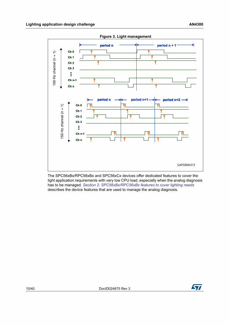
The eMIOS channels are connected to event configuration registers of the CTU, where it links an eMIOS trigger to a specified ADC channel conversion (see Figure 4). Inside each event configuration, that is connected in a fixed way to an eMIOS channel, it is possible to write an ADC channel that is triggered when an event from the eMIOS channel arrives.
Figure 4. eMIOS, ADC and CTU interconnection scheme
2.1 eMIOS (enhanced Modular Input/Output Subsystem)The SPC56EC74 includes two identical eMIOS modules that together provide up to 64 channels with input and output capability. Each eMIOS module provides 32 channels with OPWMT mode, especially suited for the lighting application. In OPWMT mode, a channel is in PWM mode, making it possible to configure a compare match, anywhere in the period, to
SPC56xBx/RPC56xBx features to cover lighting needs AN4300
12/40 DocID024675 Rev 3
trigger—using the CTU—an analog-to-digital conversion at a specified point of the period. This is especially suited for lighting applications.
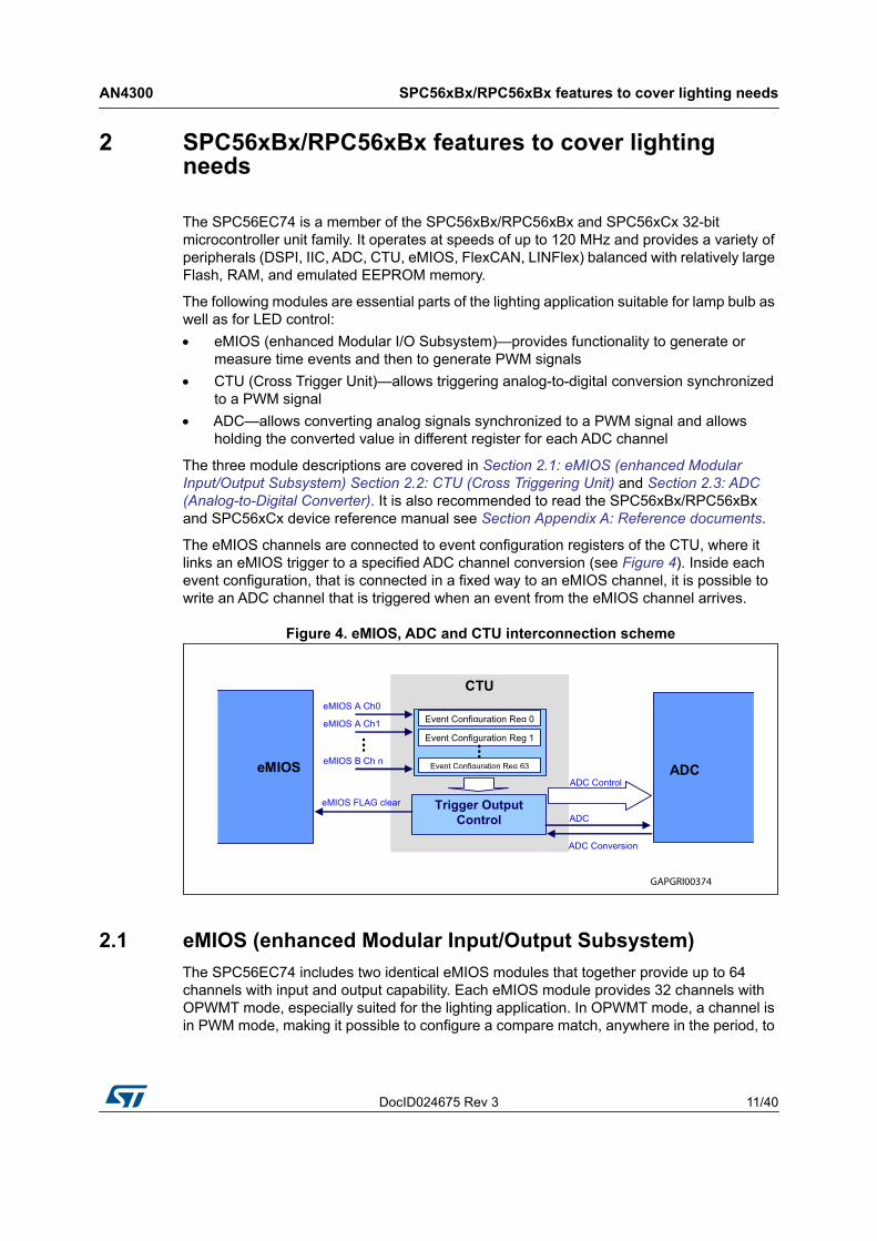
When configuring channels UC[0], UC[8], UC[16], UC[23], and UC[24] in modulus Counter Mode (MC), the A1 register determines the counting period.
Figure 5. eMIOS-OPWMT mode
When configuring a channel in OPWMT mode, the channel can be linked to: Internal counter (only for the channels that have this feature) Counter bus A driven by UC[23] Counter buses B, C, D, E driven by UC[0], UC[8], UC[16], UC[24]
In a channel configured in OPWMT mode, the A1 register value defines the PWM leading-edge and the B1 register value defines the PWM trailing edge (duty cycle). The A2 register is the sampling point for diagnostic purposes (the ADC channel trigger using the CTU), and in B2, the buffered value of the trailing edge, which is, on A1 match, loaded into the B1 register (see the eMIOS chapter of the device reference manual see Section Appendix A: Reference documents). When the B2 value equals the A1 value, the PWM duty cycle is 0 %. When a B2 value is higher than the channel period, the PWM duty cycle reaches 100 %. The PWM output signal polarity is dependent on the user’s choice.
When configuring channels UC[0], UC[8], UC[16], UC[23] and UC[24] in Modulus Counter (MC) mode, the A1 register determines the counting period.
2.2 CTU (Cross Triggering Unit)When the eMIOS OPWMT channel counter reaches the A2 value, the specific ADC channel conversion is initiated by the CTU module. The ADC channel number is specified in the CTU event configuration register by the user. When configuring the event configuration register, be aware, that: The CTU channel 0–15 event can trigger any of the ADC channels 0–15 The CTU channel 32-47 event can trigger any of the ADC channels 32–47 The CTU channel 48–95 event can trigger any of ADC channels 48–95
For more details, see the Cross Triggering Unit chapter in the device reference manual (see Section Appendix A: Reference documents).

DocID024675 Rev 3 13/40
AN4300 SPC56xBx/RPC56xBx features to cover lighting needs
39
2.3 ADC (Analog-to-Digital Converter)The 2 ADC module convert analog signals into digital form; ADC_0 with a 10-bit resolution and ADC_1 with a 12-bit resolution offering normal, injected and trigger-injected modes. The ADC module can be configured to provide up to 62 single-ended input channels with no additional external logic, expandable to 90 channels using an external multiplexer, all driven by the ADC module logic.
When using the SPC56EC74: The ADC channels 0–15 correspond to ANP pins 0–15 with a resolution of 10-bit or 12-
bit (depending on the choice of ADC_0 (10-bit resolution) or ADC_1 (12-bit resolution); in both cases the used pins are the same (precision channels)
The ADC_0 channels 32–60 (28 channels) correspond to ANS pins 0–27 (extended channel, medium occurrence) while the ADC_1 channels 32-44 correspond to ANS pins 0-12
The ADC channels 64–95 correspond to ANX pins 0–3 (external multiplexer driven by MA0–2 ADC pins; external channel, medium accuracy)
For the family SPC56xBx/RPC56xBx/SPC56xCx, 6 + 3 analog watchdogs (6 on 10-bit ADC, 3 on 12-bit ADC) are present on the ADC peripheral.
The analog watchdogs provide the capability to generate an interrupt for continuous hardware monitoring to determine if the converted channel value lies within a given guarded area defined by user-specified threshold values. If the converted value lies outside the guarded area, an interrupt is generated. The analog watchdog interrupts are well suited for light bulb diagnostic purposes.
With SPC56xBx/RPC56xBx/SPC56xCx devices, the diagnosis value can be collected in hardware mode, thus reducing the load on the CPU for this task. Moreover, one time within an input signal period, a load is placed on the CPU when these values collected in hardware mode are checked and when they are compared to certain thresholds.
The analog watchdog feature can reduce this CPU load by triggering an interrupt only when a fault occurs, instead of one time for the period, because the diagnosis check is performed in automatic mode.
Lighting application example architecture AN4300
14/40 DocID024675 Rev 3
3 Lighting application example architecture
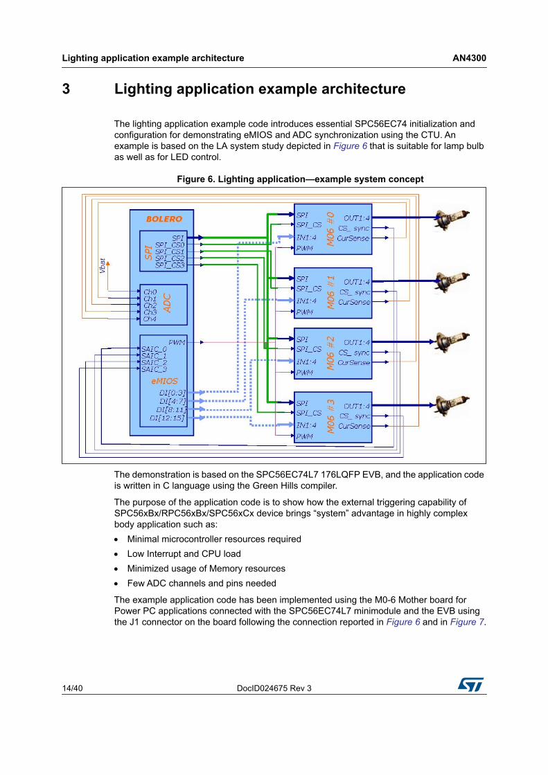
The lighting application example code introduces essential SPC56EC74 initialization and configuration for demonstrating eMIOS and ADC synchronization using the CTU. An example is based on the LA system study depicted in Figure 6 that is suitable for lamp bulb as well as for LED control.
Figure 6. Lighting application—example system concept
The demonstration is based on the SPC56EC74L7 176LQFP EVB, and the application code is written in C language using the Green Hills compiler.
The purpose of the application code is to show how the external triggering capability of SPC56xBx/RPC56xBx/SPC56xCx device brings “system” advantage in highly complex body application such as: Minimal microcontroller resources required Low Interrupt and CPU load Minimized usage of Memory resources Few ADC channels and pins needed
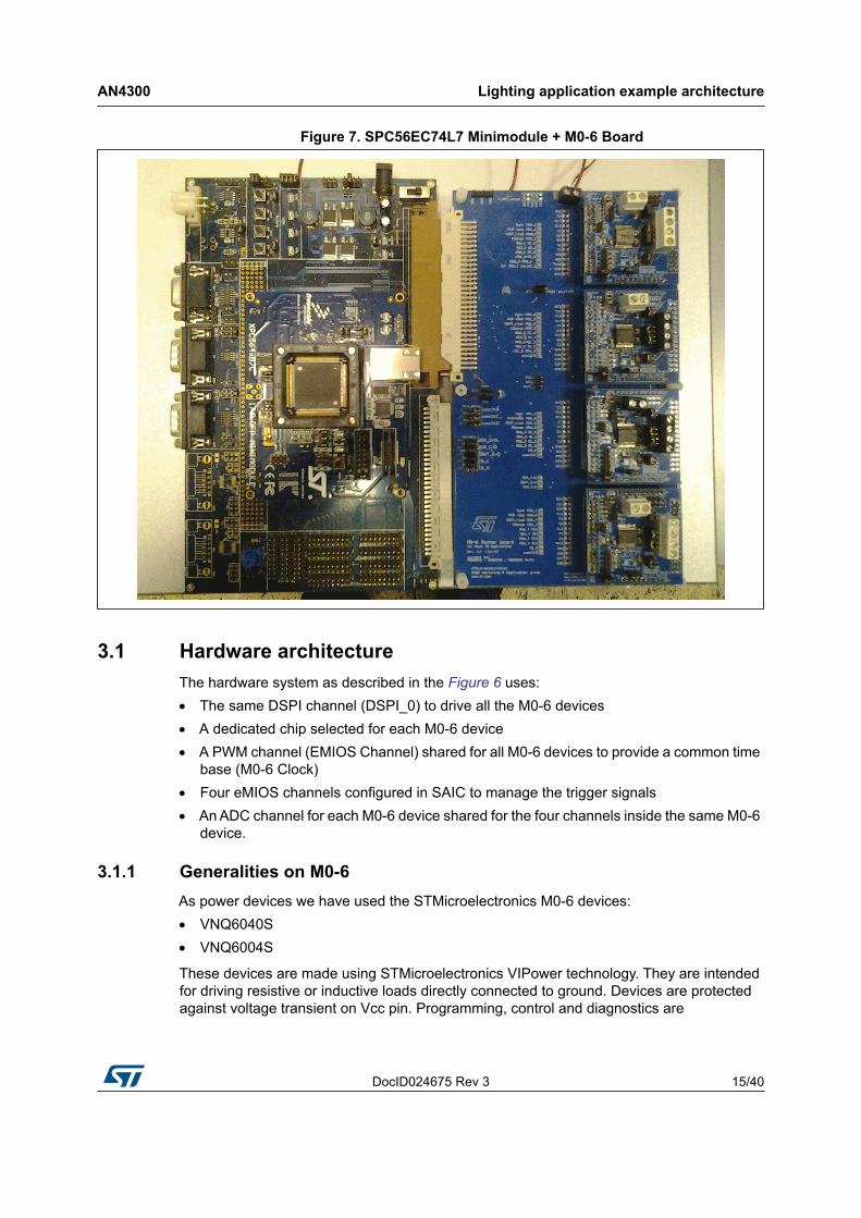
The example application code has been implemented using the M0-6 Mother board for Power PC applications connected with the SPC56EC74L7 minimodule and the EVB using the J1 connector on the board following the connection reported in Figure 6 and in Figure 7.
DocID024675 Rev 3 15/40
AN4300 Lighting application example architecture
39
Figure 7. SPC56EC74L7 Minimodule + M0-6 Board
3.1 Hardware architectureThe hardware system as described in the Figure 6 uses: The same DSPI channel (DSPI_0) to drive all the M0-6 devices A dedicated chip selected for each M0-6 device A PWM channel (EMIOS Channel) shared for all M0-6 devices to provide a common time
base (M0-6 Clock) Four eMIOS channels configured in SAIC to manage the trigger signals An ADC channel for each M0-6 device shared for the four channels inside the same M0-6
device.
3.1.1 Generalities on M0-6As power devices we have used the STMicroelectronics M0-6 devices: VNQ6040S VNQ6004S
These devices are made using STMicroelectronics VIPower technology. They are intended for driving resistive or inductive loads directly connected to ground. Devices are protected against voltage transient on Vcc pin. Programming, control and diagnostics are
Lighting application example architecture AN4300
16/40 DocID024675 Rev 3
implemented via the SPI Bus through the dedicated pins. Each device offers four channels that can drive different loads in term of power.
3.2 Software ImplementationThe software implements the following features:
Support of the SPI configuration of 16 channel of four M0-6
Adapt the PWM signal to drive the loads to the V_bat variations
Collect the current sense values for each channel and for each period
Low CPU load to collect the Current Sense
The code allows to initialize the configuration of M0-6 devices and at the beginning of each period (10 msec) performs the following steps:
Vbat Measurement via ADC
Duty cycle update for all channels of M0-6 devices
SPI frame for new information configuration
Digital diagnosis on all M0-6 devices
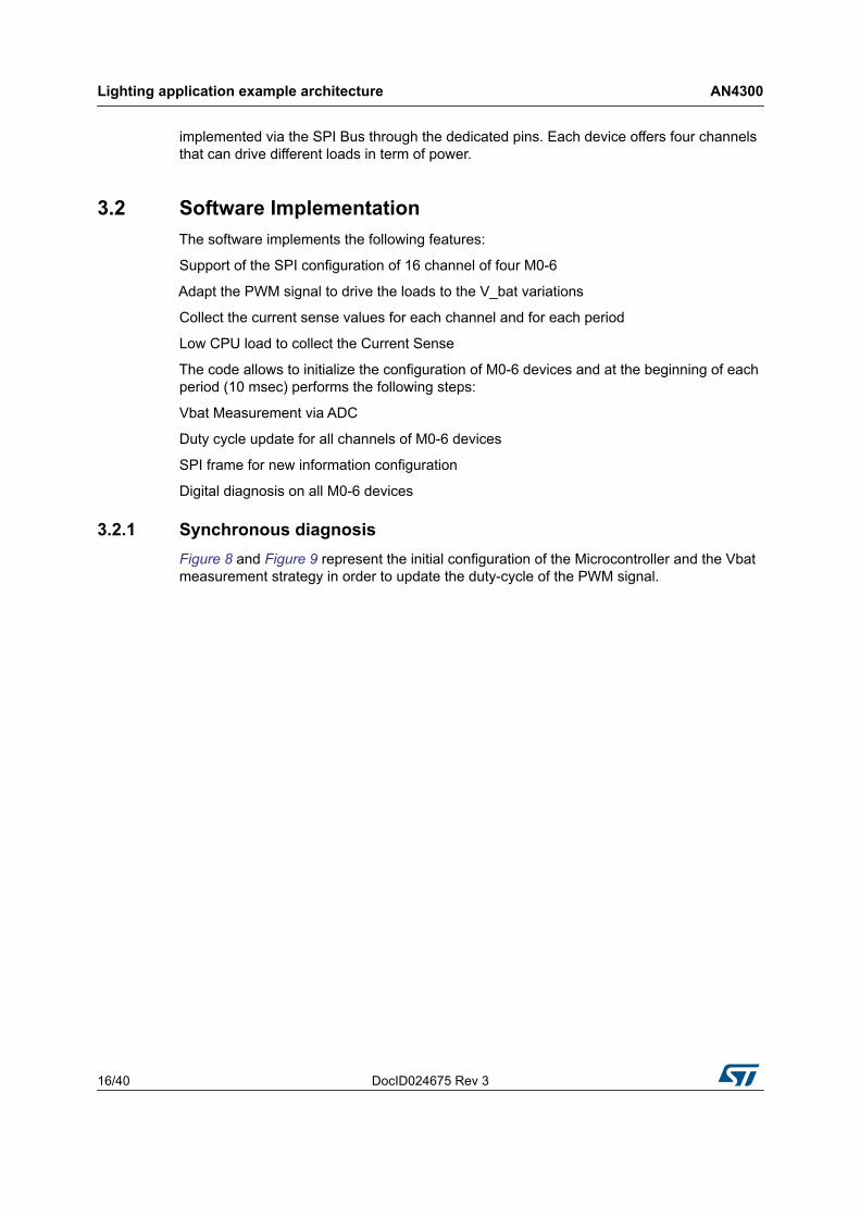
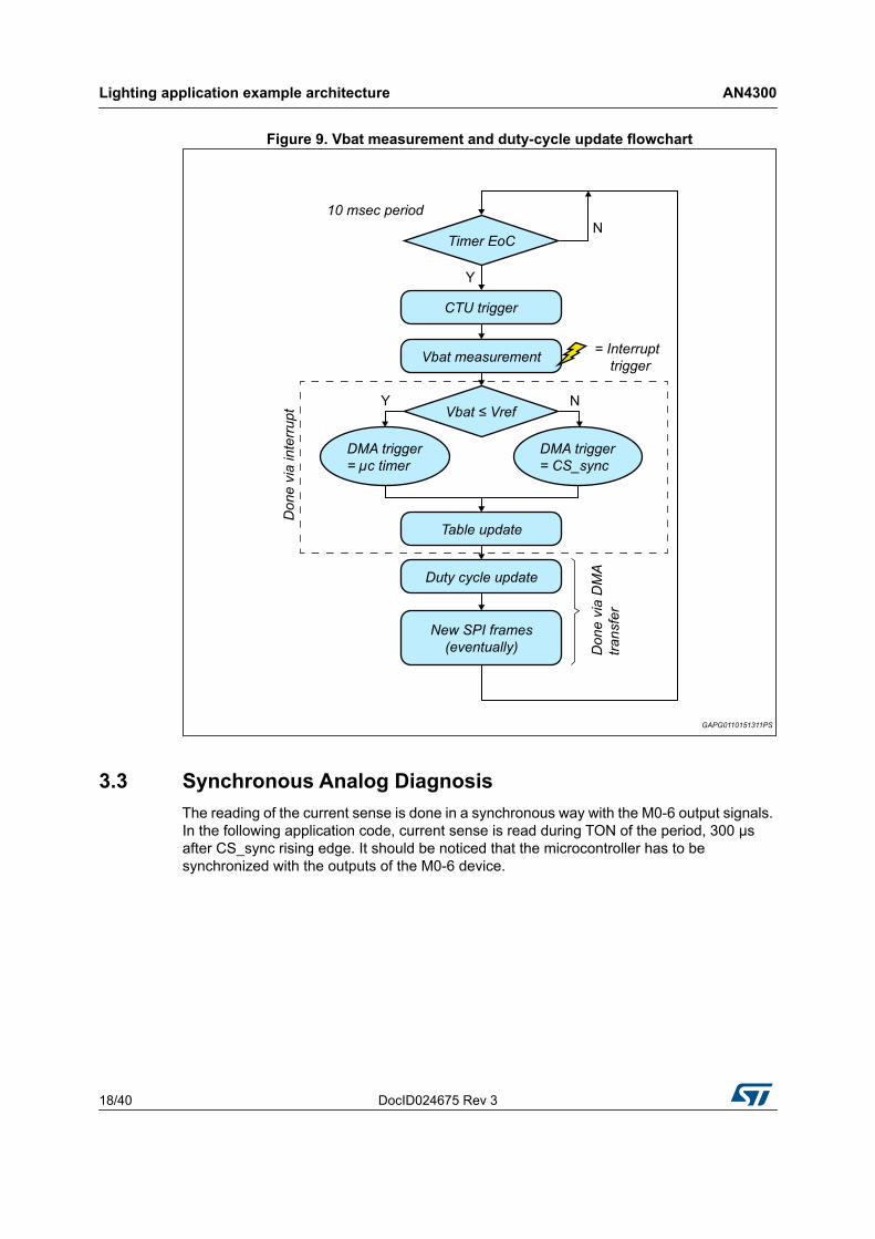
3.2.1 Synchronous diagnosisFigure 8 and Figure 9 represent the initial configuration of the Microcontroller and the Vbat measurement strategy in order to update the duty-cycle of the PWM signal.
DocID024675 Rev 3 17/40
AN4300 Lighting application example architecture
39
Figure 8. Initial Configuration flowchart
Lighting application example architecture AN4300
18/40 DocID024675 Rev 3
Figure 9. Vbat measurement and duty-cycle update flowchart
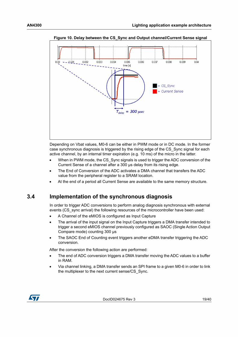
3.3 Synchronous Analog DiagnosisThe reading of the current sense is done in a synchronous way with the M0-6 output signals. In the following application code, current sense is read during TON of the period, 300 μs after CS_sync rising edge. It should be noticed that the microcontroller has to be synchronized with the outputs of the M0-6 device.
DocID024675 Rev 3 19/40
AN4300 Lighting application example architecture
39
Figure 10. Delay between the CS_Sync and Output channel/Current Sense signal
Depending on Vbat values, M0-6 can be either in PWM mode or in DC mode. In the former case synchronous diagnosis is triggered by the rising edge of the CS_Sync signal for each active channel, by an internal timer expiration (e.g. 10 ms) of the micro in the latter. When in PWM mode, the CS_Sync signals is used to trigger the ADC conversion of the
Current Sense of a channel after a 300 μs delay from its rising edge. The End of Conversion of the ADC activates a DMA channel that transfers the ADC
value from the peripheral register to a SRAM location. At the end of a period all Current Sense are available to the same memory structure.
3.4 Implementation of the synchronous diagnosisIn order to trigger ADC conversions to perform analog diagnosis synchronous with external events (CS_sync arrival) the following resources of the microcontroller have been used: A Channel of the eMIOS is configured as Input Capture The arrival of the input signal on the Input Capture triggers a DMA transfer intended to
trigger a second eMIOS channel previously configured as SAOC (Single Action Output Compare mode) counting 300 μs
The SAOC End of Counting event triggers another eDMA transfer triggering the ADC conversion.
After the conversion the following action are performed: The end of ADC conversion triggers a DMA transfer moving the ADC values to a buffer
in RAM. Via channel linking, a DMA transfer sends an SPI frame to a given M0-6 in order to link
the multiplexer to the next current sense/CS_Sync.
MCU initialization AN4300
20/40 DocID024675 Rev 3
4 MCU initialization
In this section are described the most significant functions used in the application example code.
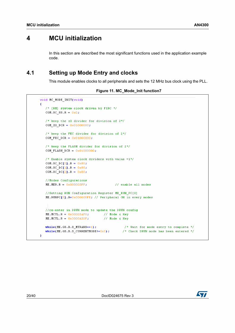
4.1 Setting up Mode Entry and clocksThis module enables clocks to all peripherals and sets the 12 MHz bus clock using the PLL.
Figure 11. MC_Mode_Init function7
DocID024675 Rev 3 21/40
AN4300 MCU initialization
39
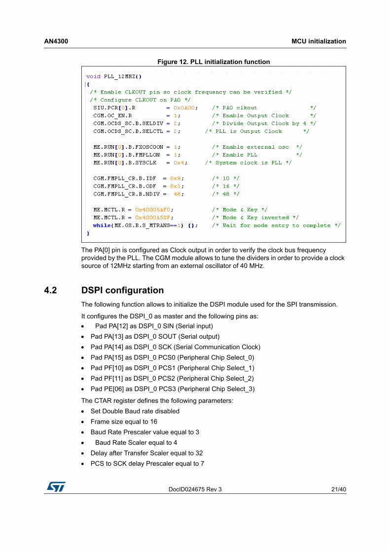
Figure 12. PLL initialization function
The PA[0] pin is configured as Clock output in order to verify the clock bus frequency provided by the PLL. The CGM module allows to tune the dividers in order to provide a clock source of 12MHz starting from an external oscillator of 40 MHz.
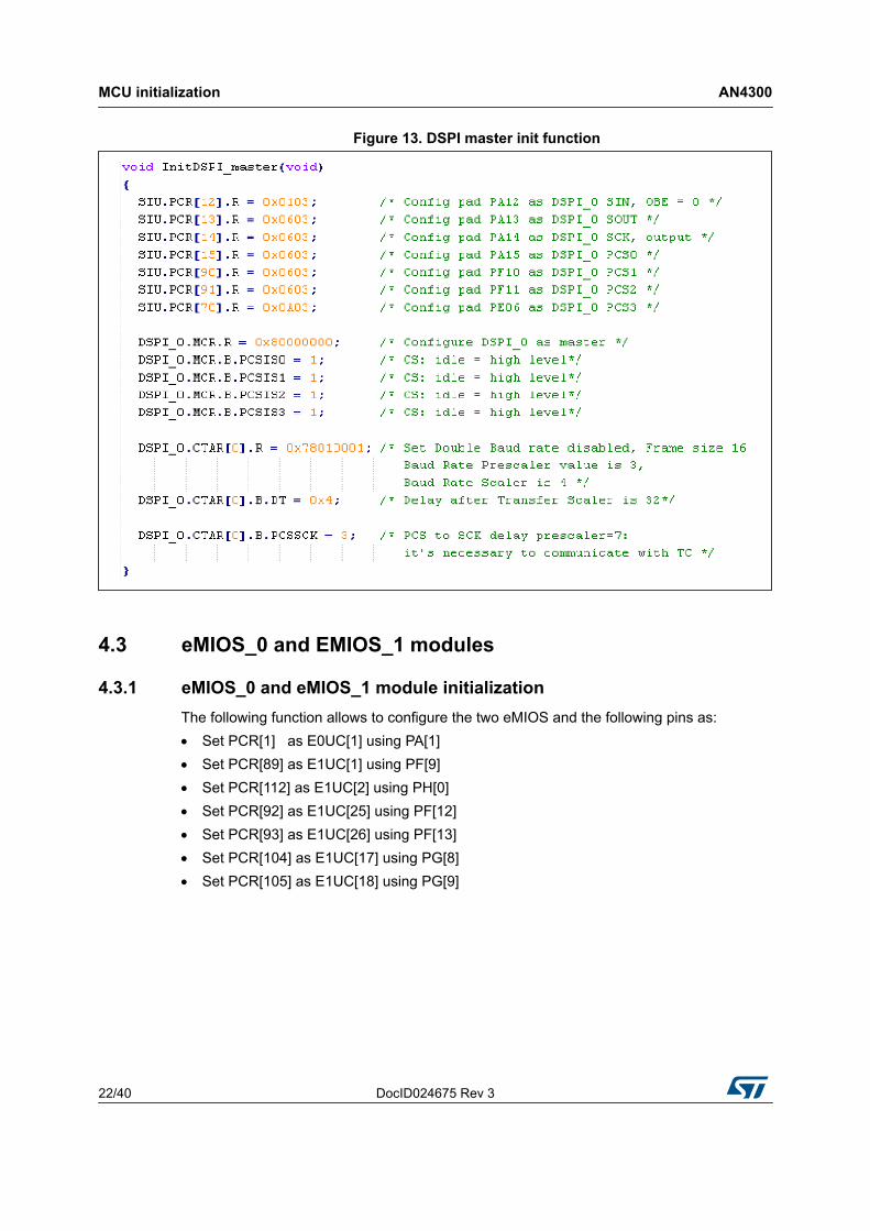
4.2 DSPI configurationThe following function allows to initialize the DSPI module used for the SPI transmission.
It configures the DSPI_0 as master and the following pins as: Pad PA[12] as DSPI_0 SIN (Serial input) Pad PA[13] as DSPI_0 SOUT (Serial output) Pad PA[14] as DSPI_0 SCK (Serial Communication Clock) Pad PA[15] as DSPI_0 PCS0 (Peripheral Chip Select_0) Pad PF[10] as DSPI_0 PCS1 (Peripheral Chip Select_1) Pad PF[11] as DSPI_0 PCS2 (Peripheral Chip Select_2) Pad PE[06] as DSPI_0 PCS3 (Peripheral Chip Select_3)
The CTAR register defines the following parameters: Set Double Baud rate disabled Frame size equal to 16 Baud Rate Prescaler value equal to 3 Baud Rate Scaler equal to 4 Delay after Transfer Scaler equal to 32 PCS to SCK delay Prescaler equal to 7
MCU initialization AN4300
22/40 DocID024675 Rev 3
Figure 13. DSPI master init function
4.3 eMIOS_0 and EMIOS_1 modules
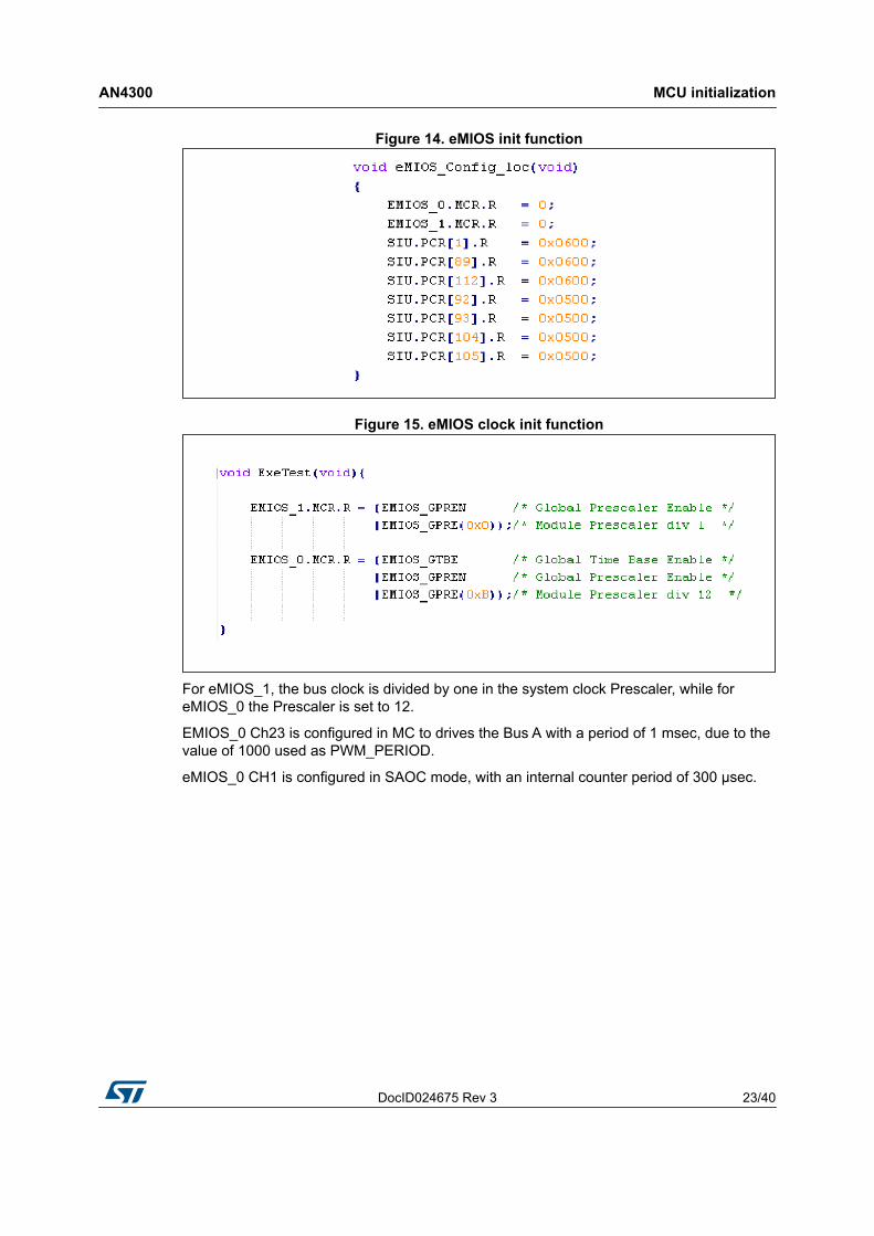
4.3.1 eMIOS_0 and eMIOS_1 module initializationThe following function allows to configure the two eMIOS and the following pins as: Set PCR[1] as E0UC[1] using PA[1] Set PCR[89] as E1UC[1] using PF[9] Set PCR[112] as E1UC[2] using PH[0] Set PCR[92] as E1UC[25] using PF[12] Set PCR[93] as E1UC[26] using PF[13] Set PCR[104] as E1UC[17] using PG[8] Set PCR[105] as E1UC[18] using PG[9]
DocID024675 Rev 3 23/40
AN4300 MCU initialization
39
Figure 14. eMIOS init function
Figure 15. eMIOS clock init function
For eMIOS_1, the bus clock is divided by one in the system clock Prescaler, while for eMIOS_0 the Prescaler is set to 12.
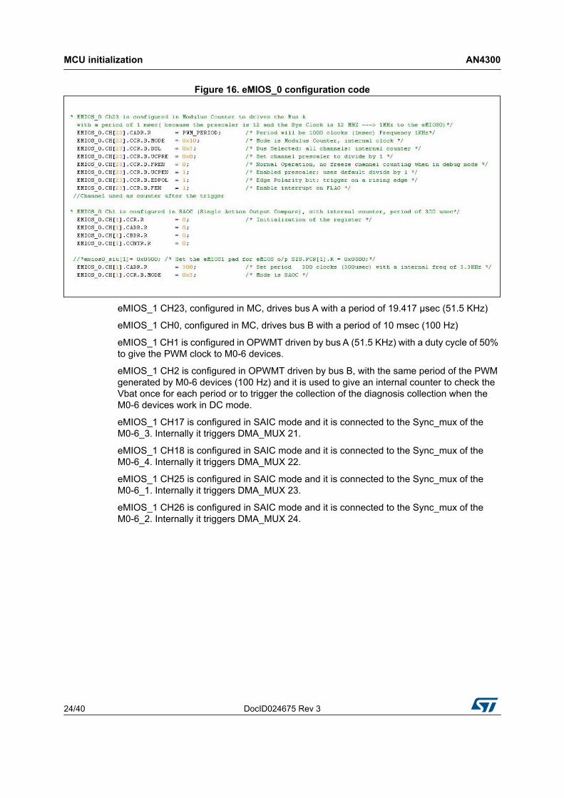
EMIOS_0 Ch23 is configured in MC to drives the Bus A with a period of 1 msec, due to the value of 1000 used as PWM_PERIOD.
eMIOS_0 CH1 is configured in SAOC mode, with an internal counter period of 300 μsec.
MCU initialization AN4300
24/40 DocID024675 Rev 3
Figure 16. eMIOS_0 configuration code
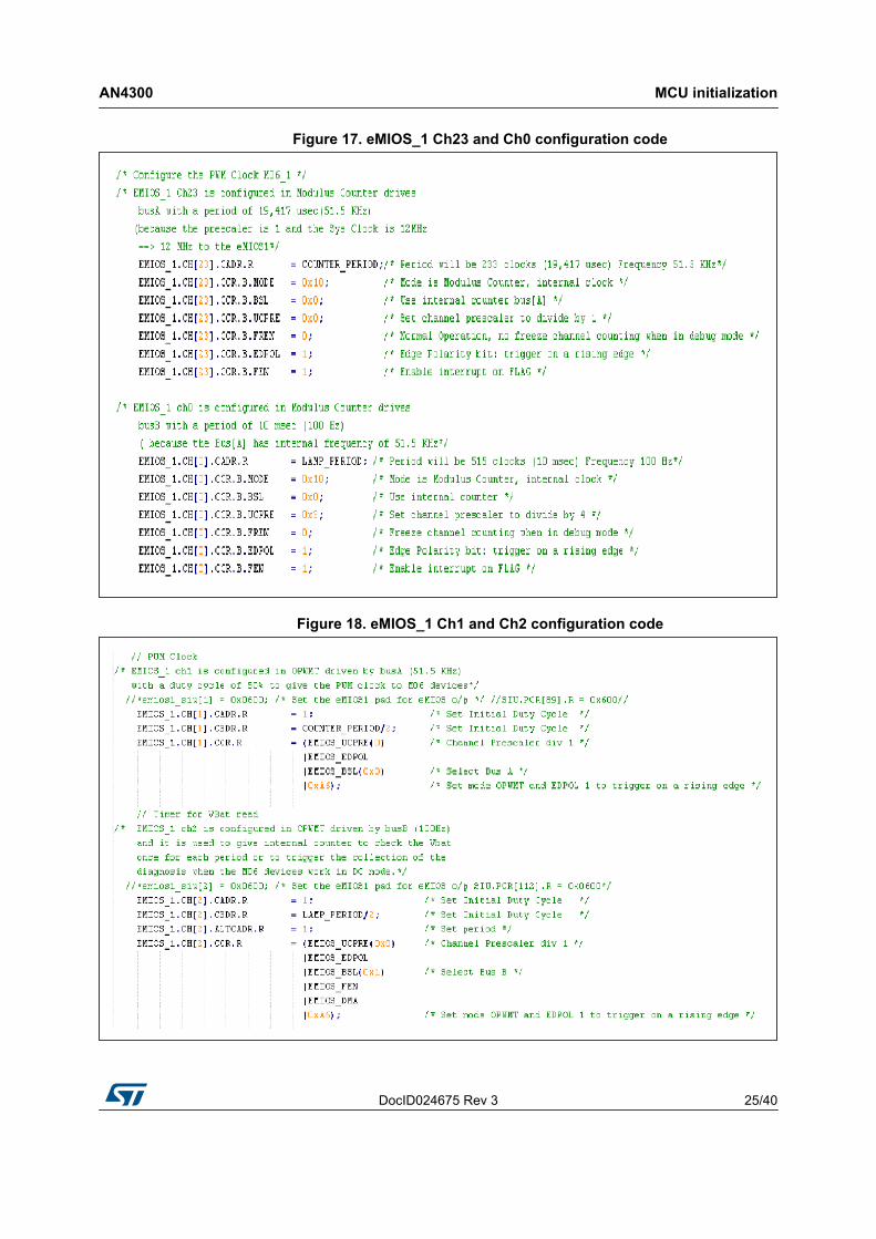
eMIOS_1 CH23, configured in MC, drives bus A with a period of 19.417 μsec (51.5 KHz)
eMIOS_1 CH0, configured in MC, drives bus B with a period of 10 msec (100 Hz)
eMIOS_1 CH1 is configured in OPWMT driven by bus A (51.5 KHz) with a duty cycle of 50% to give the PWM clock to M0-6 devices.
eMIOS_1 CH2 is configured in OPWMT driven by bus B, with the same period of the PWM generated by M0-6 devices (100 Hz) and it is used to give an internal counter to check the Vbat once for each period or to trigger the collection of the diagnosis collection when the M0-6 devices work in DC mode.
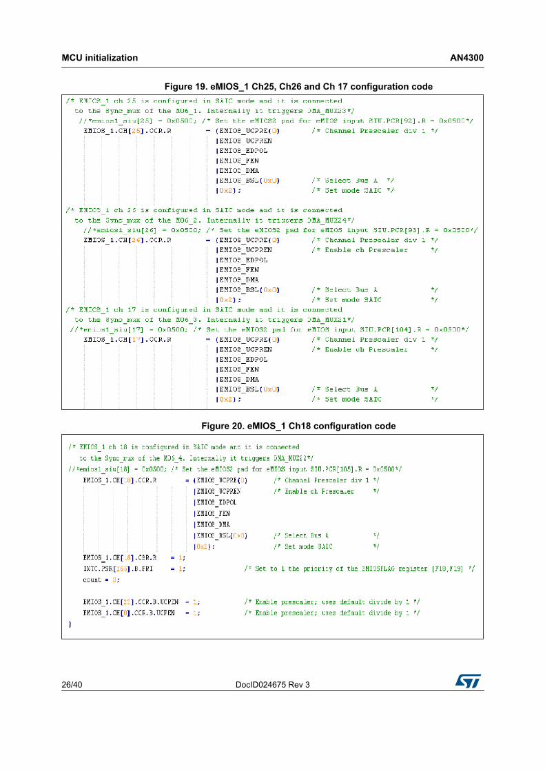
eMIOS_1 CH17 is configured in SAIC mode and it is connected to the Sync_mux of the M0-6_3. Internally it triggers DMA_MUX 21.
eMIOS_1 CH18 is configured in SAIC mode and it is connected to the Sync_mux of the M0-6_4. Internally it triggers DMA_MUX 22.
eMIOS_1 CH25 is configured in SAIC mode and it is connected to the Sync_mux of the M0-6_1. Internally it triggers DMA_MUX 23.
eMIOS_1 CH26 is configured in SAIC mode and it is connected to the Sync_mux of the M0-6_2. Internally it triggers DMA_MUX 24.
DocID024675 Rev 3 25/40
AN4300 MCU initialization
39
Figure 17. eMIOS_1 Ch23 and Ch0 configuration code
Figure 18. eMIOS_1 Ch1 and Ch2 configuration code
MCU initialization AN4300
26/40 DocID024675 Rev 3
Figure 19. eMIOS_1 Ch25, Ch26 and Ch 17 configuration code
Figure 20. eMIOS_1 Ch18 configuration code
DocID024675 Rev 3 27/40
AN4300 MCU initialization
39
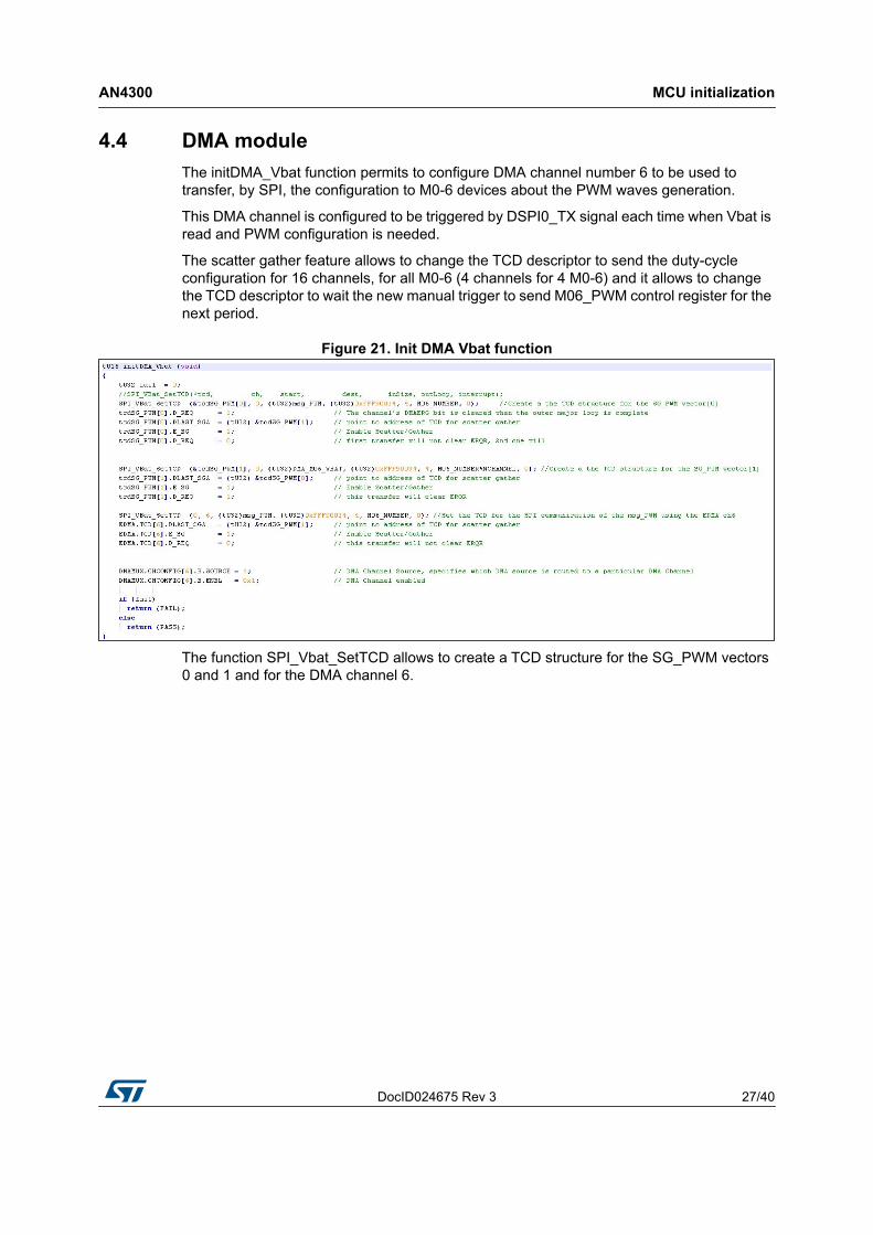
4.4 DMA moduleThe initDMA_Vbat function permits to configure DMA channel number 6 to be used to transfer, by SPI, the configuration to M0-6 devices about the PWM waves generation.
This DMA channel is configured to be triggered by DSPI0_TX signal each time when Vbat is read and PWM configuration is needed.
The scatter gather feature allows to change the TCD descriptor to send the duty-cycle configuration for 16 channels, for all M0-6 (4 channels for 4 M0-6) and it allows to change the TCD descriptor to wait the new manual trigger to send M06_PWM control register for the next period.
Figure 21. Init DMA Vbat function
The function SPI_Vbat_SetTCD allows to create a TCD structure for the SG_PWM vectors 0 and 1 and for the DMA channel 6.
MCU initialization AN4300
28/40 DocID024675 Rev 3
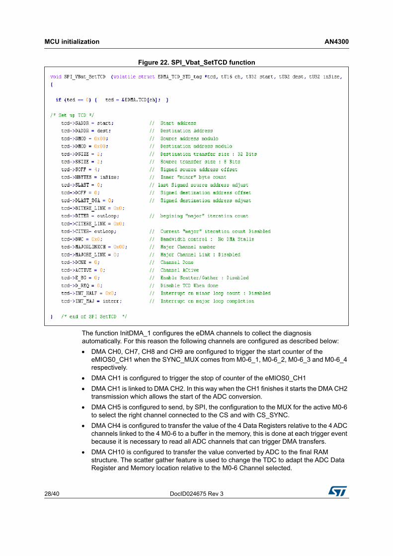
Figure 22. SPI_Vbat_SetTCD function
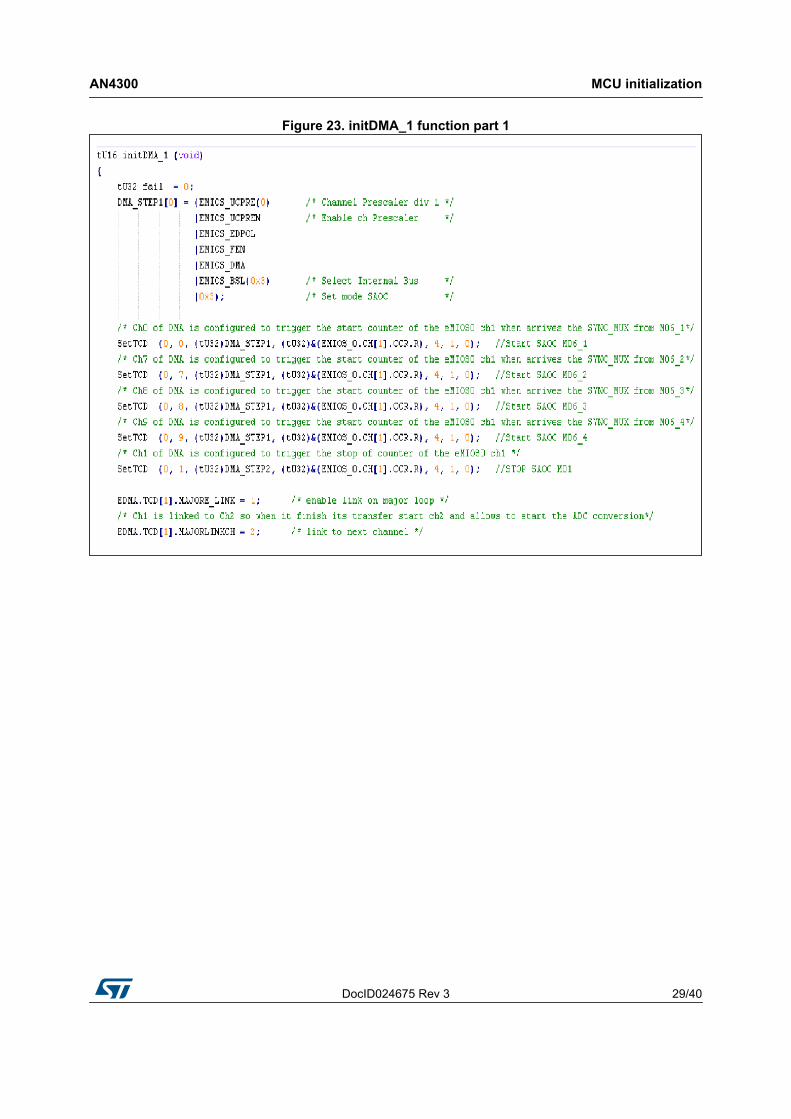
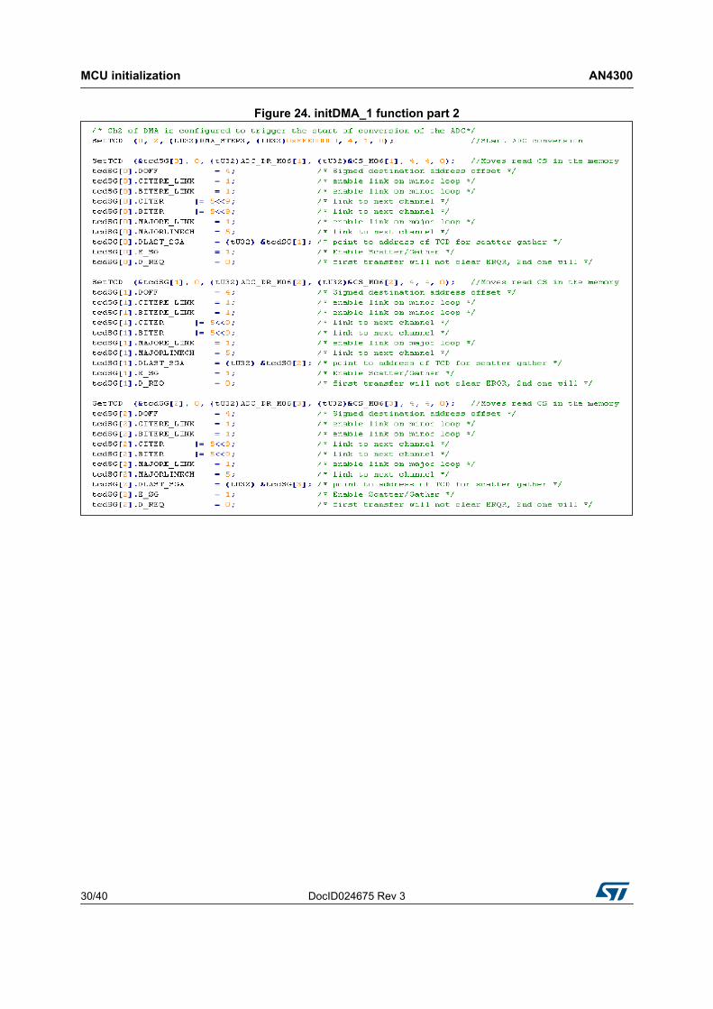
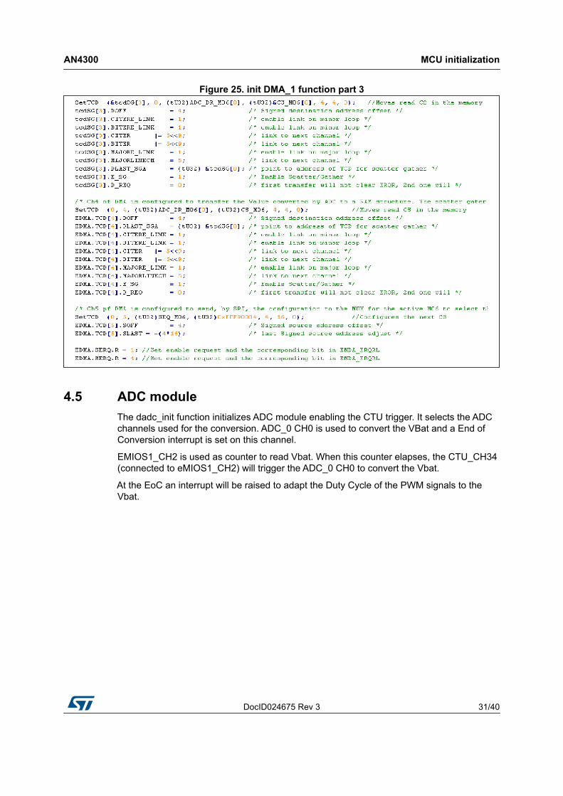
The function InitDMA_1 configures the eDMA channels to collect the diagnosis automatically. For this reason the following channels are configured as described below: DMA CH0, CH7, CH8 and CH9 are configured to trigger the start counter of the
eMIOS0_CH1 when the SYNC_MUX comes from M0-6_1, M0-6_2, M0-6_3 and M0-6_4 respectively.
DMA CH1 is configured to trigger the stop of counter of the eMIOS0_CH1 DMA CH1 is linked to DMA CH2. In this way when the CH1 finishes it starts the DMA CH2
transmission which allows the start of the ADC conversion. DMA CH5 is configured to send, by SPI, the configuration to the MUX for the active M0-6
to select the right channel connected to the CS and with CS_SYNC. DMA CH4 is configured to transfer the value of the 4 Data Registers relative to the 4 ADC
channels linked to the 4 M0-6 to a buffer in the memory, this is done at each trigger event because it is necessary to read all ADC channels that can trigger DMA transfers.
DMA CH10 is configured to transfer the value converted by ADC to the final RAM structure. The scatter gather feature is used to change the TDC to adapt the ADC Data Register and Memory location relative to the M0-6 Channel selected.
DocID024675 Rev 3 29/40
AN4300 MCU initialization
39
Figure 23. initDMA_1 function part 1
MCU initialization AN4300
30/40 DocID024675 Rev 3
Figure 24. initDMA_1 function part 2
DocID024675 Rev 3 31/40
AN4300 MCU initialization
39
Figure 25. init DMA_1 function part 3
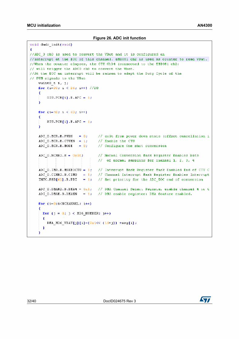
4.5 ADC moduleThe dadc_init function initializes ADC module enabling the CTU trigger. It selects the ADC channels used for the conversion. ADC_0 CH0 is used to convert the VBat and a End of Conversion interrupt is set on this channel.
EMIOS1_CH2 is used as counter to read Vbat. When this counter elapses, the CTU_CH34 (connected to eMIOS1_CH2) will trigger the ADC_0 CH0 to convert the Vbat.
At the EoC an interrupt will be raised to adapt the Duty Cycle of the PWM signals to the Vbat.
MCU initialization AN4300
32/40 DocID024675 Rev 3
Figure 26. ADC init function
DocID024675 Rev 3 33/40
AN4300 MCU initialization
39
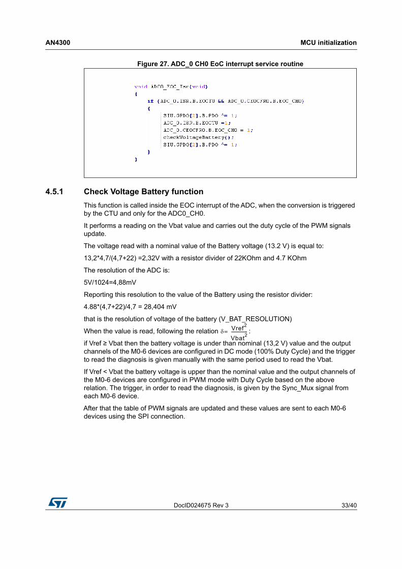
Figure 27. ADC_0 CH0 EoC interrupt service routine
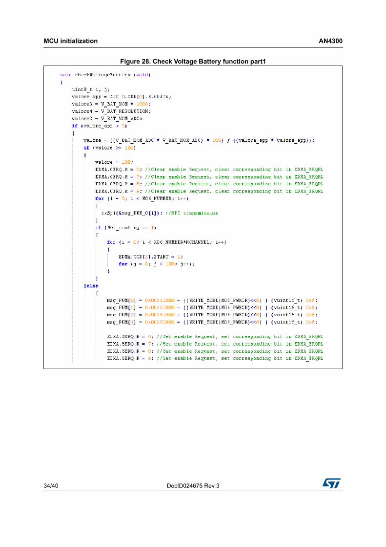
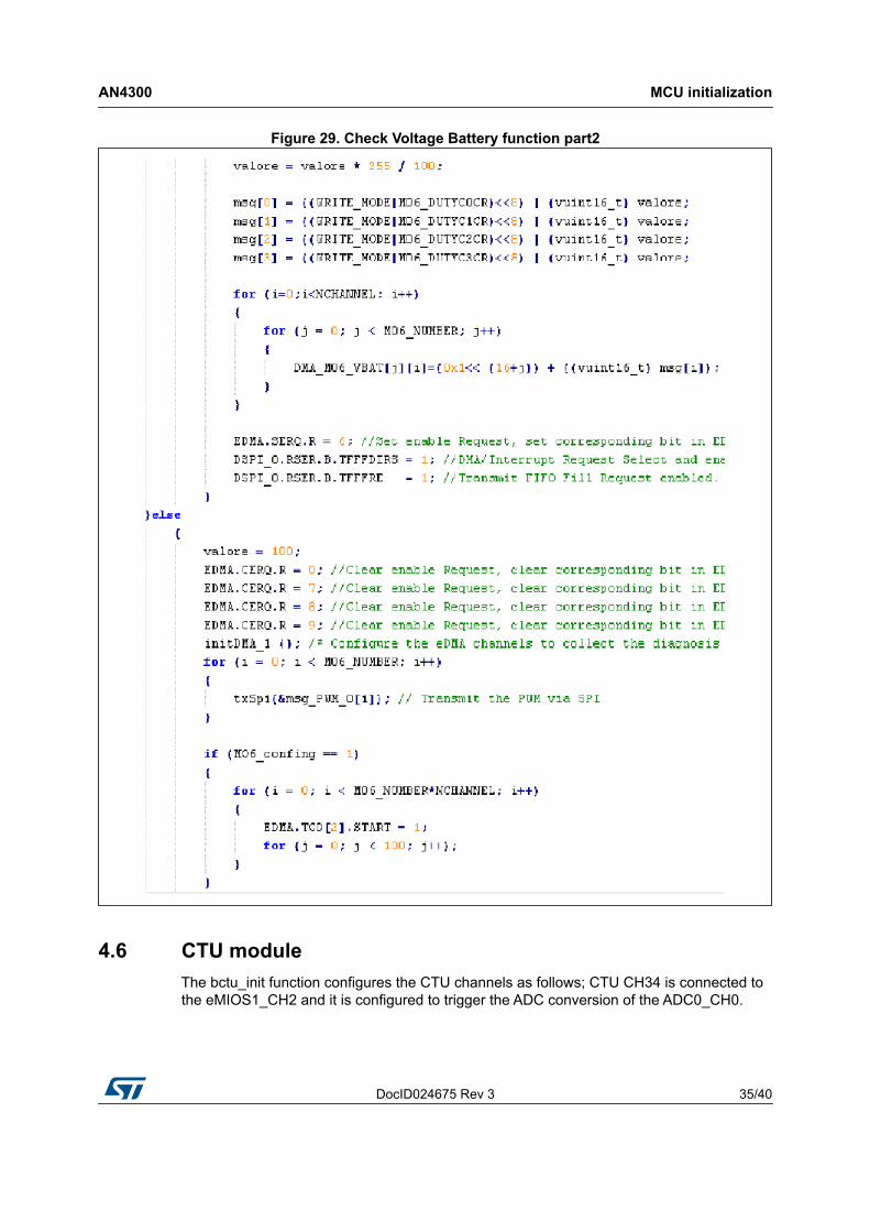
4.5.1 Check Voltage Battery functionThis function is called inside the EOC interrupt of the ADC, when the conversion is triggered by the CTU and only for the ADC0_CH0.
It performs a reading on the Vbat value and carries out the duty cycle of the PWM signals update.
The voltage read with a nominal value of the Battery voltage (13.2 V) is equal to:
13,2*4,7/(4,7+22) =2,32V with a resistor divider of 22KOhm and 4.7 KOhm
The resolution of the ADC is:
5V/1024=4,88mV
Reporting this resolution to the value of the Battery using the resistor divider:
4.88*(4,7+22)/4,7 = 28,404 mV
that is the resolution of voltage of the battery (V_BAT_RESOLUTION)
When the value is read, following the relation :
if Vref ≥ Vbat then the battery voltage is under than nominal (13,2 V) value and the output channels of the M0-6 devices are configured in DC mode (100% Duty Cycle) and the trigger to read the diagnosis is given manually with the same period used to read the Vbat.
If Vref < Vbat the battery voltage is upper than the nominal value and the output channels of the M0-6 devices are configured in PWM mode with Duty Cycle based on the above relation. The trigger, in order to read the diagnosis, is given by the Sync_Mux signal from each M0-6 device.
After that the table of PWM signals are updated and these values are sent to each M0-6 devices using the SPI connection.
Vref2
Vbat2----------------=
MCU initialization AN4300
34/40 DocID024675 Rev 3
Figure 28. Check Voltage Battery function part1
DocID024675 Rev 3 35/40
AN4300 MCU initialization
39
Figure 29. Check Voltage Battery function part2
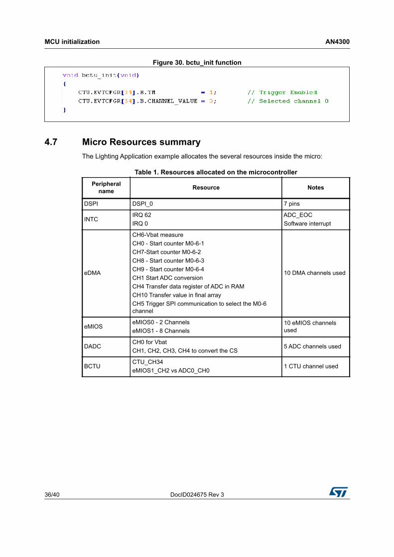
4.6 CTU moduleThe bctu_init function configures the CTU channels as follows; CTU CH34 is connected to the eMIOS1_CH2 and it is configured to trigger the ADC conversion of the ADC0_CH0.
MCU initialization AN4300
36/40 DocID024675 Rev 3
Figure 30. bctu_init function
4.7 Micro Resources summaryThe Lighting Application example allocates the several resources inside the micro:
Table 1. Resources allocated on the microcontrollerPeripheral
name Resource Notes
DSPI DSPI_0 7 pins
INTCIRQ 62IRQ 0
ADC_EOCSoftware interrupt
eDMA
CH6-Vbat measureCH0 - Start counter M0-6-1CH7-Start counter M0-6-2CH8 - Start counter M0-6-3CH9 - Start counter M0-6-4CH1 Start ADC conversionCH4 Transfer data register of ADC in RAMCH10 Transfer value in final arrayCH5 Trigger SPI communication to select the M0-6 channel
10 DMA channels used
eMIOSeMIOS0 - 2 ChannelseMIOS1 - 8 Channels
10 eMIOS channels used
DADCCH0 for VbatCH1, CH2, CH3, CH4 to convert the CS
5 ADC channels used
BCTUCTU_CH34eMIOS1_CH2 vs ADC0_CH0
1 CTU channel used
DocID024675 Rev 3 37/40
AN4300 Conclusion
39
5 Conclusion
The SPC56EC74 lighting application example introduces MCU eMIOS, CTU, and ADC modules usage within a lighting application, which is in this case well suited for the lamp light bulbs control as well as for the lamp LEDs control with no major change required in the peripherals software.
The benefit of using the CTU module is significant as opposed to using the timer to trigger ADC at a certain point within a PWM channel cycle. The timer produces frequent interrupts that need to be processed by the MCU CPU, causing an increase in the CPU load and suspending run time processes. Using the CTU gives the application designer a powerful tool to avoid diagnostic timer-configuration challenges and makes the lighting application simpler to design and test.
The ADC module gives the designer the opportunity to use watchdog threshold interrupts to increase MCU performance, and enables fast responses in case of lamp light bulb failures. If required, the number of the ADC channels can be increased from 64 up to 95, using simple external logic circuitry fully controlled by the ADC module.
The eMIOS module offers up to 64 PWM channels suitable for a lighting application as well as for other PWM-based applications. The eMIOS module provides PWM channels with high resolution and flexibility.
The lighting application example consists of an example description and complete software demonstration based on the SPC56EC74L7 LQFP176 minimodule and EVB.
This example is easily portable to each device of the SPC56xBx/RPC56xBx/SPC56xCx family; for devices which have DMA module, no particular modifications are required. For devices where DMA module is missing, the DMA feature can be replaced with interrupt routines but with a higher CPU load.
Reference documents AN4300
38/40 DocID024675 Rev 3
Appendix A Reference documents
A.1 Reference documents SPC560B4x, SPC560B5x, SPC560C4x, SPC560C5x, 32-bit MCU family built on the
embedded Power Architecture® (RM0017), available at www.st.com SPC564Bxx, SPC56ECxx 32-bit MCU family built on the embedded Power
Architecture® (RM0070 DOC ID18196)
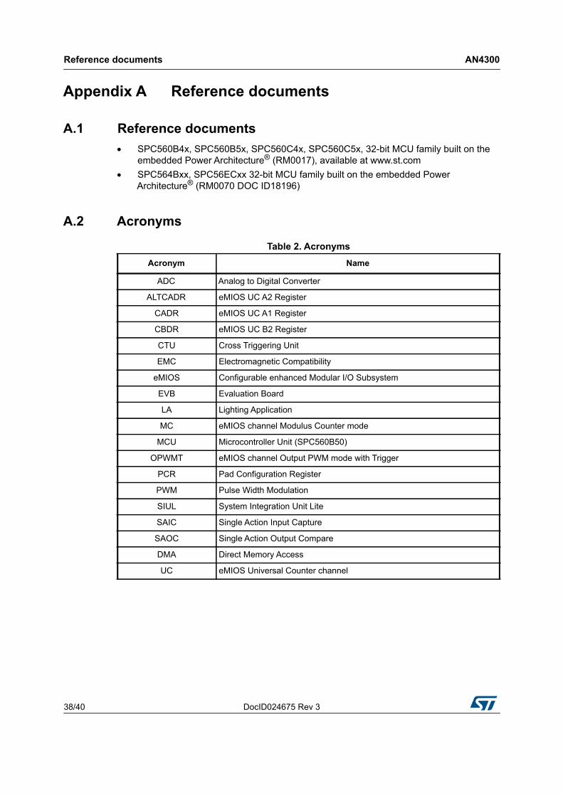
A.2 Acronyms
Table 2. AcronymsAcronym Name
ADC Analog to Digital Converter
ALTCADR eMIOS UC A2 Register
CADR eMIOS UC A1 Register
CBDR eMIOS UC B2 Register
CTU Cross Triggering Unit
EMC Electromagnetic Compatibility
eMIOS Configurable enhanced Modular I/O Subsystem
EVB Evaluation Board
LA Lighting Application
MC eMIOS channel Modulus Counter mode
MCU Microcontroller Unit (SPC560B50)
OPWMT eMIOS channel Output PWM mode with Trigger
PCR Pad Configuration Register
PWM Pulse Width Modulation
SIUL System Integration Unit Lite
SAIC Single Action Input Capture
SAOC Single Action Output Compare
DMA Direct Memory Access
UC eMIOS Universal Counter channel

DocID024675 Rev 3 39/40
AN4300 Revision history
39
Revision history
Table 3. Document revision history Date Revision Changes
13-Jun-2013 1 Initial release
17-Sep-2013 2 Updated Disclaimer.
08-Oct-2015 3 Robust root part numbers added.

AN4300
40/40 DocID024675 Rev 3
IMPORTANT NOTICE – PLEASE READ CAREFULLY
STMicroelectronics NV and its subsidiaries (“ST”) reserve the right to make changes, corrections, enhancements, modifications, and improvements to ST products and/or to this document at any time without notice. Purchasers should obtain the latest relevant information on ST products before placing orders. ST products are sold pursuant to ST’s terms and conditions of sale in place at the time of order acknowledgement.
Purchasers are solely responsible for the choice, selection, and use of ST products and ST assumes no liability for application assistance or the design of Purchasers’ products.
No license, express or implied, to any intellectual property right is granted by ST herein.
Resale of ST products with provisions different from the information set forth herein shall void any warranty granted by ST for such product.
ST and the ST logo are trademarks of ST. All other product or service names are the property of their respective owners.
Information in this document supersedes and replaces information previously supplied in any prior versions of this document.
© 2015 STMicroelectronics – All rights reserved


![No Model VIN 1 (DM) SANTAFE [DM] KMHSU81BSCU000212 2 … Engine YF and D… · 37 (dm) santafe [dm] kmhst81bsdu023920 38 (dm) santafe [dm] kmhst81bsdu023926 39 (dm) santafe [dm] kmhst81bsdu023930](https://img.pdfslide.us/doc/110x75/6017564e29e54a6dde7ebe6b/no-model-vin-1-dm-santafe-dm-kmhsu81bscu000212-2-engine-yf-and-d-37-dm-santafe.jpg)