Embed Size (px)
Citation preview
Advanced Lab Course
Composition Analysis on Heterostructure Lasers
M215
Stand: 2016-04-08
Aim: Nanoscale composition analysis by Transmission Electron Microscopy
Content
1 The JEOL JEM2100 2 1.1 Alignments ..................................................................................................................... 2
2. Fundamental Physics of Electron Microscopy ................................................................... 3
2.1 Electron beam-matter interactions ............................................................................... 3
3 Scientific Background: FundamentalPhysics and Notation ................................................. 6
3.1 AlxGa1−xAs/GaAs heterostructures for laser applications ..................................... 6
3.2 Composition analysis of AlxGa1−xAs/GaAs het- erostructures by Transmission Electron Microscopy ............................................................................................................ 6
4 Experimental Procedure .................................................................................................. 12
4.1 Epitaxial growth ........................................................................................................ 12
4.2 TEM sample preparation .......................................................................................... 12
4.3 TEM-investigation ..................................................................................................... 12
5 Evaluation of the experiment ....................................................................................... 13
6 Questions to be answered in your report...................................................................... 14
M215: Composition Analysis on Heterostructure Lasers
2
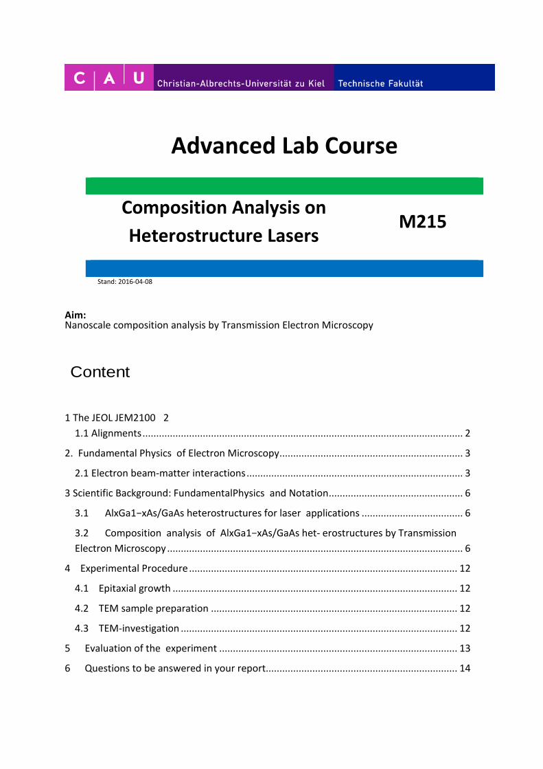
1 The JEOL JEM2100
Figure 1: Setup of the JEM2100 JEOL microscope
1.1 Alignments
In order to record the best possible images with the highest possible resolution the microscope has to be properly aligned before every use. This is necessary because not all components of the microscope are exactly on the optical axis, apertures have been used and are misaligned or slight changes in the environment influenced the microscope. These alignments comprise of centering the electron beam, all apertures in use (at least the condenser aperture, optionally also the diffraction and objective aperture) and correcting the pivot points when tilting the electron beam. On top of that, instrumental aberrations like astigmatism have to be corrected. Other aberrations, like the chromatic and spherical aberration can only be corrected in some special microscopes with dedicated correctors for every aberration.

M215: Composition Analysis on Heterostructure Lasers
3
2. Fundamental Physics of Electron Microscopy
2.1 Electron beam-matter interactions In general the interaction between the electron beam of the microscope and the sample to be analyzed can be categorized into two fields: inelastic interactions where the electrons loose some fraction of their kinetic energy, and elastic interactions where incoming and outgoing kinetic energy of the electron is equal. Note that from each and every interaction between electron beam and sample we can gather some kind of information, but not every interaction can be detected. An overview of various interactions is depicted in Fig. 2. As mentioned before, not all of them can be detected, even though their information might be useful. Typically, TEMs are equipped with EDX detectors above the sample and various electron detectors below the sample, hence other interactions such as secondary electrons, backscattered electrons, Auger electrons, heat and cathodoluminescence signals cannot be detected. Reasons for that are manifold and in general it is possible to equip TEMs with according detectors, but simply not needed, because their information is redundant or the signal is generally too weak to be detected.
Figure 2: Overview of different electron beam-matter interactions.
The most useful information can be extracted from scattered electrons, however also the unscattered transmitted electron beam bears valuable information. In order for a specimen to be analyzable in TEMs its thickness must be well below 200 nm, otherwise no beam is transmitted at all, neither scattered nor unscattered. Besides the high intensity of the unscattered transmitted beam the elastically scattered electrons make up the highest fraction of interaction outcomes.

M215: Composition Analysis on Heterostructure Lasers
4
Among them are electrons that were deflected by an atomic core in the sample while maintaining their complete kinetic energy. However, diffraction according to the Bragg-condition is also an elastic process, hence diffracted electrons also count towards this group. Inelastic scattering processes are much more diversified. Electrons can lose kinetic energy to all interactions above the specimen, indicated in Fig. 2. Hence, they can excite Auger electrons, characteristic X-rays, light emission, secondary electrons and of course create heat. On top of that, knock-on damage – ballistically altering the appearance of the sample – can occur, which unlike the other interactions is of course unwanted. But it is not only their interaction products but also the inelastically scattered electrons themselves because their energy loss is just as characteristic as their interaction product. If, for example, the beam excites a core electron of a sample containing iron from the L to the M shell this excitation causes the emission of Fe Lα radiation with an energy of 708 eV, but in turn a portion of the beam must also loose exactly 708 eV, which can be detected as well, with the appropriate apparatus. Other interactions, such as the above mentioned SE, BSE and AE electrons are typically of most interest in SEMs and are not recorded in TEMs. From these interactions various kinds of contrast modes can be extracted. In the most simple case mass-thickness contrast is recorded in the bright field mode, much alike traditional light microscopy. Areas of the sample that are thicker or that contain “heavier” elements (high atomic number Z) scatter more electrons and are thus darker; this is called Z-contrast. The opposite of the bright field signal is called dark field. In dark field mode, either elastically or inelastically scattered electrons can be recorded, thus thick areas or areas with heavy elements appear bright. However, since interactions are complex and manifold, no “pure” Z-contrast is ever recorded but always a combination of different contrast modes. Another one is diffraction contrast, which like the name suggests is created by Bragg-diffraction. Crystalline areas of the sample which are oriented so that the Bragg condition is fulfilled appear darker in bright field mode, because a larger fraction of electrons is scattered (diffracted) in this area. More complicated are contrast modes like phase contrast used for high-resolution imaging. Here, the unscattered and elastic diffracted beams create contrast by interference with each other. Fig. 3 gives an overview of the above mentioned and some other analysis techniques, not all of which are going to be used in this lab course.

M215: Composition Analysis on Heterostructure Lasers
5
Figure 3: Overview of various analysis methods based on different electron beam-sample interactions. In this lab course you are going to utilize phase contrast, Z-contrast, selected area diffraction and energy dispersive X-ray spectroscopy to analyze and unknown sample.

M215: Composition Analysis on Heterostructure Lasers
6
3 Scientific Background: FundamentalPhysics and Notation
3.1 AlxGa1−xAs/GaAs heterostructures for laser applications The semiconductor alloy AlxGa1−xAs is used as a material in heterostructure lasers. An advantageous property of the ternary alloy is that it is almost fully lattice matched with GaAs for all values of x. Thick defect-free layers of the alloy can therefore be grown epitaxially on GaAs substrates. A further impor- tant property of AlxGa1−xAs is the direct band gap up to Al-concentrations of about x = 0.4.
In heterostructure lasers AlxGa1−xAs with the larger band gap compared to GaAs serves as the barrier material. The active layer is made from GaAs. The charge carriers are trapped in the active layer and recombine radiativly. Quantum confinement occurs when the active layer is made very thin (a few nanometers). The quantum confinement greatly alters the density of states in the active layer. This effect can be exploited for the reduction of the threshold current of the laser structure.
The wavelength of the emitted light is determined by the band gap of the active layer. By using AlxGa1−xAs with low x values instead of GaAs in the active layer the wavelength can be tuned via the choice of x. This effect is used in heterostructure lasers without quantum confinement (thick active layers). For thin active layers the layer thickness as well affects the wavelength of the emitted light because the energy states in the valence and conduction bands depend on the width of the quantum well.
3.2 Composition analysis of AlxGa1−xAs/GaAs het- erostructures by Transmission Electron Microscopy For the production of heterostructure lasers based on the AlxGa1−xAs/GaAs system it is important to precisely control not only the overall Al-concentration x in the AlxGa1−xAs layers but also to make sure that the Al is homogeneously distributed in the epitaxial layer. Transmission Electron Microscopy (TEM) is a technique which allows to measure alloy concentrations on a nanometer scale. In the case of AlxGa1−xAs the strength of the Bragg reflection at {200} lattice planes turns out to be highly sensitive to the Al-concentration (see below) and is therefore exploited for the determination of the alloy composition. In the lab course we will determine the Al-concentration of four AlxGa1−xAs- layers separated from each other by GaAs-layers. Instead of evaluating a {200}
M215: Composition Analysis on Heterostructure Lasers
7
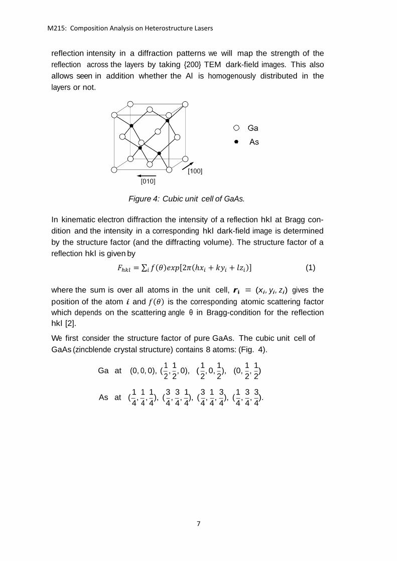
reflection intensity in a diffraction patterns we will map the strength of the reflection across the layers by taking {200} TEM dark-field images. This also allows seen in addition whether the Al is homogenously distributed in the layers or not.
Figure 4: Cubic unit cell of GaAs. In kinematic electron diffraction the intensity of a reflection hkl at Bragg con- dition and the intensity in a corresponding hkl dark-field image is determined by the structure factor (and the diffracting volume). The structure factor of a reflection hkl is given by
𝐹𝐹ℎ𝑘𝑘𝑘𝑘 = ∑ 𝑓𝑓(𝜃𝜃)𝑒𝑒𝑒𝑒𝑒𝑒[2𝜋𝜋(ℎ𝑒𝑒𝑖𝑖 + 𝑘𝑘𝑦𝑦𝑖𝑖 + 𝑙𝑙𝑧𝑧𝑖𝑖)]𝑖𝑖 (1) where the sum is over all atoms in the unit cell, ri = (xi, yi, zi) gives the position of the atom 𝑖𝑖 and 𝑓𝑓(𝜃𝜃) is the corresponding atomic scattering factor which depends on the scattering angle θ in Bragg-condition for the reflection hkl [2].
We first consider the structure factor of pure GaAs. The cubic unit cell of GaAs (zincblende crystal structure) contains 8 atoms: (Fig. 4).
1
Ga at (0, 0, 0), ( , 2
1 , 0), (
2 1
, 0, 2
1 1 1 ), (0, , )
2 2 2
1 1 As at ( , ,
4 4 1 3
), ( , 4 4
3 1 3 1 , ), ( , ,
4 4 4 4 3 1
), ( , 4 4
3 3 , ).
4 4

M215: Composition Analysis on Heterostructure Lasers
8
200
Figure 5: Sequence of the layers in the interesting part of the sample and nominal Al-concentrations.
By inserting in eq. (1) one readily obtains
Fhkl = 0 for h,k,l mixed Fhkl = 4(fGa + fAs) for h,k,l even, h + k + l = 4n Fhkl = 4(fGa + ifAs) for h,k,l odd, h + k + l = 4n + 1 Fhkl =
Fhkl =
4(fGa − fAs) 4(fGa − ifAs)
for h,k,l even, h + k + l = 4n + 2 for h,k,l odd, h + k + l = 4n + 3.
Here fGa and fAs denote the atomic scattering factors of Ga and As, respec- tively. Since the atomic scattering factors of Ga and As are nearly equal, reflections with h + k + l = 4n + 2 are almost absent in GaAs. If we replace Ga by Al, i.e. consider the pure compound AlAs, the structure amplitudes of reflections hkl with h + k + l = 4n + 2 become considerably larger because of the larger difference between the atomic scattering factors of Al and As. For this reason reflections with h + k + l = 4n + 2 are called “chemically sensitive reflections”. In the case that Al and Ga atoms are statistically mixed on the group III sublattice the structure factor of the chemically sensitive reflections depends on the Al-concentration x in the following way:
Fhkl = 4(xfAl + (1 − x)fGa − fAs) for h + k + l = 4n + 2. (2) In the following we assume that the chemically sensitive reflection (002) is set at Bragg-condition. Within the kinematical approximation which is valid for thin specimens the intensity I200 of the reflection (002) quadratically depends on both the specimen thickness t and the structure amplitude [2, 3]
I200 ∝ t2F 2 . (3)

M215: Composition Analysis on Heterostructure Lasers
9
200
− 200
a) b)
004
220
111 002
111
002
111 002
111
220
004
Laue circle Figure 6: a) Diffraction pattern in the [110] zone-axis. Many refelctions are strongly excited. b) Diffraction pattern after tilting out of the zone-axis about the [002] direction. The Laue circle corresponds to the intersection line of the Ewald sphere with the reciprocal (110) plane perpendicular. In b) fewer reflections are strongly excited.
In the experiment we will directly compare the intensities I Alx Ga1−x As(t) of the (002) reflection from a AlxGa1 xAs-layer with the intensity I GaAs(t) from a GaAs-layer. Because the two layers are next to each other in the TEM-foil we may assume an identical foil thickness t for both layers. By dividing the intensities the thickness dependence cancels out resulting in
𝑅𝑅(𝑒𝑒) = 𝐼𝐼002𝐴𝐴𝑘𝑘𝑥𝑥𝐺𝐺𝐺𝐺1−𝑥𝑥𝐴𝐴𝐴𝐴(𝑡𝑡)𝐼𝐼002𝐺𝐺𝐺𝐺𝐴𝐴𝐴𝐴(𝑡𝑡)
= 𝑒𝑒𝑓𝑓𝐴𝐴𝑘𝑘(𝜃𝜃002) + (1 − 𝑒𝑒)𝑓𝑓𝐺𝐺𝐺𝐺(𝜃𝜃002) − 𝑓𝑓𝐴𝐴𝐴𝐴(𝜃𝜃002)
𝑓𝑓𝐺𝐺𝐺𝐺(𝜃𝜃002)− 𝑓𝑓𝐴𝐴𝐴𝐴(𝜃𝜃002)
= (1 + 𝐴𝐴𝑒𝑒)2 (4)
With
𝐴𝐴 = 𝑓𝑓𝐴𝐴𝑘𝑘(𝜃𝜃002) − 𝑓𝑓𝐺𝐺𝐺𝐺(𝜃𝜃002)𝑓𝑓𝐺𝐺𝐺𝐺(𝜃𝜃002)− 𝑓𝑓𝐴𝐴𝐴𝐴(𝜃𝜃002) (5)
A is a function of the atomic scattering factors of the elements at the Bragg- angle θ002 for the (002) lattice planes. The atomic scattering factors are given in the attached list. The Al-concentration x can therefore be directly determined from the ratio R(x) without the knowledge of the specimen thickness (which is difficult to be determined accurately). Please note that this is only possible because we use GaAs with its known composition as a

M215: Composition Analysis on Heterostructure Lasers
10
reference.
The AlxGa1−xAs/GaAs-heterostructures have been deposited by metal-organic vapor phase epitaxy (MOVPE) onto a (001) oriented GaAs wafer. The layer stacking is schematically shown in Fig. 5. The nominal Al-concentrations x of the AlxGa1−xAs-layers are 0.4, 0.3, 0.2 and 0.05, respectively. For the TEM investigation a cross-sectional thin foil with [110] foil normal has already been prepared by a member of the staff. Fig. 6a shows a (110) zone axis electron diffraction pattern obtained from a thin area in the GaAs substrate with the CCD camera attached to the TEM. Because the electron beam is oriented along the zone axis many low-index reflections are simultaneously excited. In order to reduce the number of excited beams while maintaining the excitation of the (002) reflection, the sample is tilted away from the zone axis by several degrees about the [002] direction. Fig. 6b shows on the right side the effect of the tilting on the diffraction pattern. Only those reflections which are near to the Ewald-sphere are excited. The Ewald-sphere cuts the (110) reciprocal plane forming the so-called Laue circle. Part of the Laue-circle is schematically shown in Fig. 6b. The (002) reflection exactly lies on the Laue-circle because this reflection has been set to Bragg condition. Obviously, it is not possible to obtain a pure two-beam condition (only direct beam and (002) reflection) because the additional excitation of the reflections 004, 002, 004, ... can not be completely avoided.
For a more detailed discussion of the dependence of I002 on the Al- concentration and the specimen thickness including effects of the dynamical scattering and the excitation of more than only the (002) reflection Fig.8 shows numerically calculated reflection intensities as a function of t for GaAs (a) and Al0.4Ga0.6As (b). Five beams (direct beam (000) and (004), (002), (002), (004)
Figure 7: Dark-field image of the AlxGa1−xAs/GaAs heterostructure obtained with the (002) reflection. The AlxGa1−xAs layers appear bright. The brighter the contrast, the higher the Al-concentration.

M215: Composition Analysis on Heterostructure Lasers
11
Figure 8: Results of numerical calculations of the dynamical scattering. Five beams are included (direct beam (000), (002), (004), (00-2), (00-4)) with (002) set at Bragg-condition. a) and b): “Pendelloesung”-results (reflection inten- sities versus sample thickness) for GaAs and Al0.4Ga0.6As, respectively. Only the intensities of (000) and (002) are shown for simplicity. The chemically sen- sitive (002) reflection builds up much faster in Al0.4Ga0.6As than in the GaAs. c) Ratio of the the (002) intensities of Al0.4Ga0.6As and GaAs. (Dashed lines: kinematical results).
with (002) set to Bragg-condition (cf. Fig.3) were included in the fully dynam- ical simulation. However, only the intensities of 000 and 002 are shown. The simulations were performed with a program by J.M. Zuo [4] which uses the Blochwave method for the evaluation of the dynamical scattering process. As expected from the structure amplitudes the (002) reflection builts up much faster in Al0.4Ga0.6As than in GaAs. Only for small values of the sample thickness t the quadratic dependence of I002 on t expected from the kinematcal theory (eq.3) becomes visible (the “kinematical curves” are shown as dashed lines). According to Bithell and Stobbs [3], the expression for the ration R(x) (eq.4), however, can be used up to larger values of t even though the expres- sion was directly obtained from the kinematical theory eq.3. In Fig.5c the ratio R(x) determined from the two simulated I002 curves (dynamical theory)

M215: Composition Analysis on Heterostructure Lasers
12
is compared with the ratio obtained from eq.4 (kinematical theory). In a de- tailed analysis Bithell and Stobbs [3] showed that the Al-concentration deduced from a kinematical analysis, however, is systematically too large. The authors showed that this can be approximately taken into account by substracting 5% from the Al-concentration obtained via eq.4.
4 Experimental Procedure A complete experimental procedure would comprise the following steps
1. Epitaxial growth of the layers
2. TEM sample preparation
3. TEM investigation
However, because of the lack of time, the first two steps are already done and only the last part will be perfomed during the lab course.
4.1 Epitaxial growth
The epitaxial growth was performed in the group of F. Scholz at the University of Stuttgart. A GaAs(001) wafer with a miscut of 6◦ towards [110] was used as the substrate. Alternating GaAs and AlxGa1−xAs layers were grown on the top of the wafer by Metal-Organic Vapour Phase Epitaxy (MOVPE) at a temperature of 660◦. The MOVPE method is in widespread use in the fabrication of heterostructures for optoelectronic devices.
4.2 TEM sample preparation
The thin TEM foil was prepared by focused ion beam (FIB) technique.
4.3 TEM-investigation
A member of staff will mount the sample in the holder and insert the holder in the column of the microscope. He will assist you during operating the TEM.

M215: Composition Analysis on Heterostructure Lasers
13
• Make yourself familiar with the handling of the microscope. Move a thin sample area containing the AlxGa1−xAs layers under the electron beam. Take a bright field image.
• Tilt the sample in the (110) zone axis. To do that insert a selected-area
diffraction (SAD) aperture, spread the beam and take a focussed zone-axis diffraction pattern (use a camera length of 40 cm (cf. Fig.6a).
• Identify the (002) reflection in the diffraction pattern.
• Tilt the sample by several degrees about the [001] direction. Set the
(002) reflection exactly into Bragg condition (Fig. 6b). Take a focussed diffraction pattern (cf. Fig.6, right).
• Insert the smallest objective aperture in the column and center it around
the primary reflection. Under option “Operation” of the menu switch from bright to dark. Use the “Dark tilt” to shift the (002) reflection into the center. Now switch off the Diffraction modus and Take a dark-field image of the AlxGa1−xAs layers.
5 Evaluation of the experiment
• during the lab course:
– For the dark-field images take a line profile across the AlxGa1−xAs/GaAs-heterostructure in the region where the contrast of the AlxGa1−xAs layers are brightest.
– For each AlxGa1−xAs-layer determine the ratio R (cf. equation 4) by dividing the image intensity in the layer by the mean of the image intensities in the adjacent GaAs layers.
• at home:
– With the help of the tables plot the atomic scattering factors fGa, fAl and fAs as functions of the scattering angle θ in one graph. Discuss the meaning of the curves. Determine the respective scattering factors for the Bragg angle θ002 of the (002) reflection. (Interpolate linearly between the tabulated values.)
– Determine the coefficient A in eq.(4).
– With the use of eq.(4) and the values R found for the AlxGa1−xAs-

M215: Composition Analysis on Heterostructure Lasers
14
layers determine the Al-concentrations x of each AlxGa1−xAs layers. Substract 5% in order to account for dynamical effects (cf. Sec.1.2).
- Compare your results with reference data given from the
supervisor and the nominal concentration given by the crystal grower.
– Compare this method with the STEM EDX linescan data from the supervisor. Do your results fit with the state of the art technique? Discuss.
6 Questions to be answered in your report
1. What determines the intensity of a reflection in an electron diffraction pattern? Why did we use a dark-field image for determining the Al- concentration in the layers and not a (selected area) diffraction pattern?
2. Briefly explain the difference between kinematical and dynamical theory
of electron diffraction in a crystal.
3. From the experimental dark-field images what can be said about the lateral (perpendicular to the growth direction) and vertical (parallel to the growth direction) homogeneity of the Al-concentration in the AlxGa1−xAs layers. What could be possible reasons for the presence of gradients along the growth direction?

M215: Composition Analysis on Heterostructure Lasers
15
References
[1] M.J. Kelly,“Low-Dimensional Semiconductors”, Clarendon Press, Oxford 1995, ch. 18.
[2] E. Fuchs, H. Oppolzer, and H. Rehme, “Particle Beam Analysis”, VHC
Verlagsgesellschaft mbH, Weinheim 1990, ch. 4.
[3] E.G. Bithell and W.M. Stobbs, “Composition determination in the GaAs/(Al, Ga)As system using contrast in dark-field transmission elec- tron microscope images”, Phil. Mag. A, 1989, Vol. 60, No. 1, 39-62.
[4] J.H.C. Spence and J.M. Zuo, “Electron Microdiffraction”, 1992.
[5] P.A. Doyle and P.S. Turner, Acta. Cryst. A24, 390 (1968).


![Rafid Ahmed - db.in.tum.dedb.in.tum.de/.../seminarHauptspeicherdbs/slides/04-cuckoo-hashing.pdf · Fakultät für Informatik Technische Universität München Cuckoo Hashing[1] : 4](https://img.pdfslide.us/doc/110x75/5dd1338bd6be591ccb64b526/rafid-ahmed-dbintumdedbintumdeseminarhauptspeicherdbsslides04-cuckoo-.jpg)