Embed Size (px)
Citation preview

Advanced Encryption StandardFor
Smart Card Security
Aiyappan Natarajan David Jasinski
Kesava R.Talupuru Lilian Atieno
Advisor: Prof. Wayne Burleson

Outline
Recap - Aiyappan System Interface - Aiyappan Key Expansion - David Encryption 1 - Lilian Encryption 2 – Kesava Future Work – Kesava

I/P
Rdy_in
Processor FSM
Encrypt Key Sched
I/P FSM
O/P FSM
1
128
1
O/P
128
clk clkReset
clk
Reset
Ready O/P Request O/P
start
send
clkReset
Key
Sub key
System Architecture
Data/Key Reg. ModuleData/Key Reg. Module

Processor Finite State Machine
The main controller for all the other modules
Controlled by two signals Reset and start
Gets instructions stored in the memory
Decodes instructions
Enables the appropriate signals

Input Controller
Communicates with external system through a serial I/O pin
Gets the input data and key from the external system
Gives the 128-bit parallel data to data/key register module
Controlled by processor

Data/Key register module
Stores input data and key in the appropriate registers
Controlled by processor through two control signals mux_en, d_k
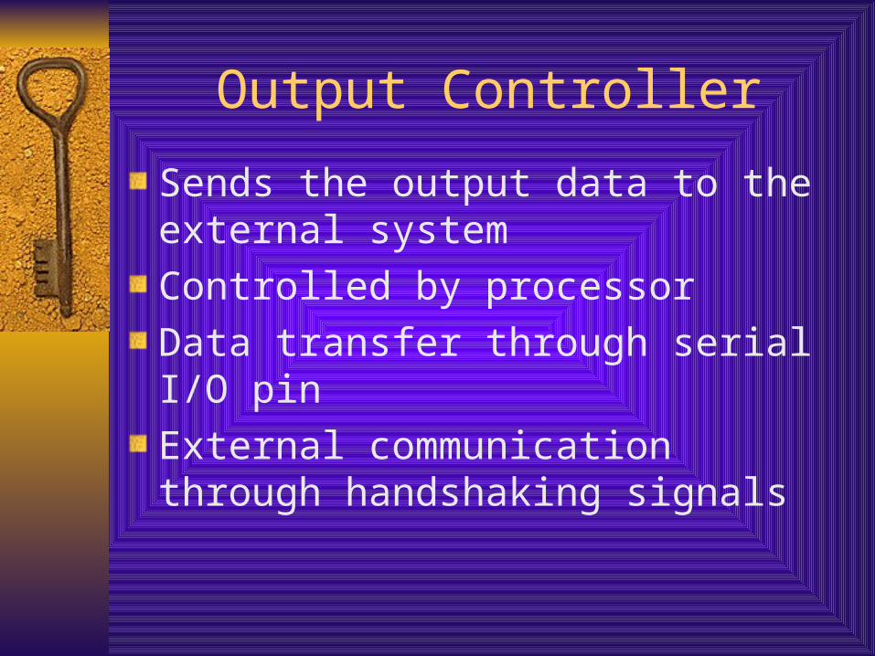
Output Controller
Sends the output data to the external system
Controlled by processor
Data transfer through serial I/O pin
External communication through handshaking signals

ExternalExternalSystemSystem
InputInput
ControllerController
FSMFSM
Processor Processor
FSMFSM
Data/Key Data/Key RegisterRegister
Serial I/OSerial I/O
sendsend
Rdy_inRdy_in Rdy_OutRdy_Out
rec_datarec_data
clkclk ResetReset clkclk
128128
Parallel DataParallel Data
ResetReset
Mux_enMux_en d_kd_k
clkclk
128128
128128
DataData
KeyKey
Processor – Input Controller InterfaceProcessor – Input Controller Interface
PCPC
instrinstr
2
3

Simulation Results

Simulation Results (contd.)

Processor - Output Controller InterfaceProcessor - Output Controller Interface
Encrypted DataEncrypted DataExternalExternalSystemSystem
OutputOutput
ControllerController
FSMFSM
Processor Processor
FSMFSM
Serial I/OSerial I/O
clkclk
128128
clkclkSend_dataSend_data
Data_rdyData_rdy
ResetReset
sentsentOutput_dataOutput_data
instrinstr PCPC
2
3

Simulation Results

Work completed
RTL code for all the modules
Test bench for each module
Simulation for each module
Integrated the Processor , Data/key register, Input and Output controller
Test bench for the integrated top module
Simulation for the top module

Work to be done
Integrate the Encryption core and Key scheduling core along with the interface
Test Bench for the entire interface Synthesize each module Simulation for synthesized netlist Synthesize the total integrated module Simulation for the entire system
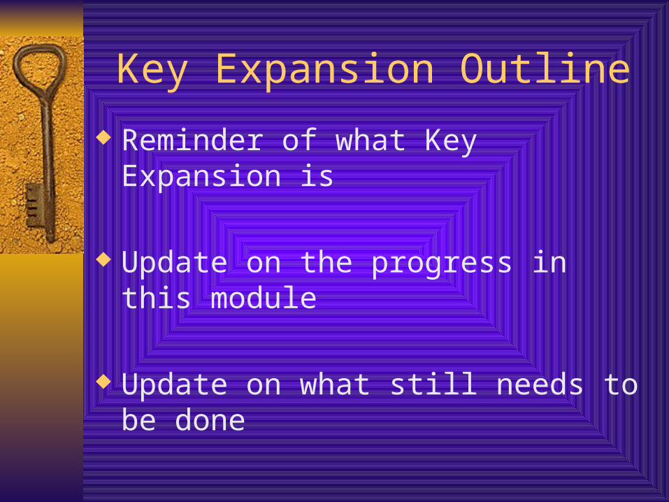
Key Expansion Outline
Reminder of what Key Expansion is
Update on the progress in this module
Update on what still needs to be done
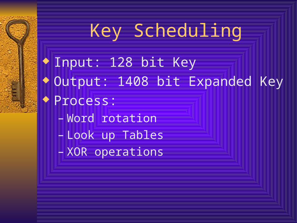
Key Scheduling
Input: 128 bit Key Output: 1408 bit Expanded Key Process:
– Word rotation– Look up Tables– XOR operations

Completed Work
Behavioral Model (~481 lines of verilog code) RTL code (~422 lines of verilog code)
Synthesized RTL code (~30,000 gates)– With warnings
Error Propagation

Behavioral Functionality

Synthesized Design

Error Propagation
0
100
200
300
400
500
600
700
1 8 15 22 29 36 43 50 57 64 71 78 85 92 99 106 113 120 127
Position of the Bit Changed in the Original Key
Nu
mb
er o
f B
its
Ch
ang
ed o
n t
he
Exp
and
ed K
ey
Errors For EveryBit Change
Average Per 4Byte WordSection

What Needs to Be Done
Power Analysis
Gate Level Timing Analysis
Design Optimization

ShiftRow() Transformation
- 128 bit data is broken down into four rows
-Each of the 32-bit rows contains 4 bytes.
-The first row is not shifted.
-The last three rows of the State are byte-wise cyclically shifted as shown in the next slide.

S 0,0 S 0,1 S 0,2 S 0,3
S 1,0 S 1,1 S 1,2 S 1,3
S 2,0 S 2,1 S 2,2 S 2,3
S 3,0 S 3,1 S 3,2 S 3,3
S 0,0 S 0,1 S 0,2 S 0,3
S 1,1 S 1,2 S 1,3 S 1,0
S 2,2 S 2,3 S 2,0 S 2,1
S 3,3 S 3,0 S 3,1 S 3,2
no shift

30
02010103
03020101
01030201
01010302
'
'
'
'
,3
,2
,1
,0
,3
,2
,1
,0
cfor
S
S
S
S
S
S
S
S
C
C
C
C
C
C
C
C
Mix column() Transformation
- Operates on State column-by-column.
- Each column is treated as a four-term polynomial.
-The four bytes in the four “rows” are used for matrix multiplication in GF(28) as shown below.
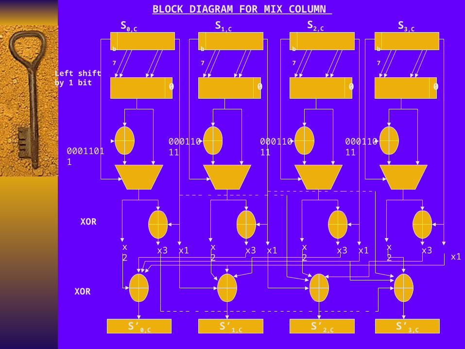
BLOCK DIAGRAM FOR MIX COLUMN
00011011
Left shiftby 1 bit
x1
S’0,C
x2 x3 x1
b
7
0
S’1,C
x2 x3 x1
b
7
0
S’2,C
x2 x3 x1
b
7
0
S’3,C
x2 x3
b
7
0
00011011
00011011
00011011
S0,C S2,C S3,CS1,C
XOR
XOR

Key Add Substitution Shift Row Mix Column Key Add
SubstitutionShift RowKey Add
Sub Key
Sub Key
ED
Raw Data
Encryption Algorithm Flow
Sub Key Repeat (Round-1) times

Sub_bytes Transformation
S S S
8 8 8
8 8 8
S S S
8 8 8
8 8 8
……
Input
Output
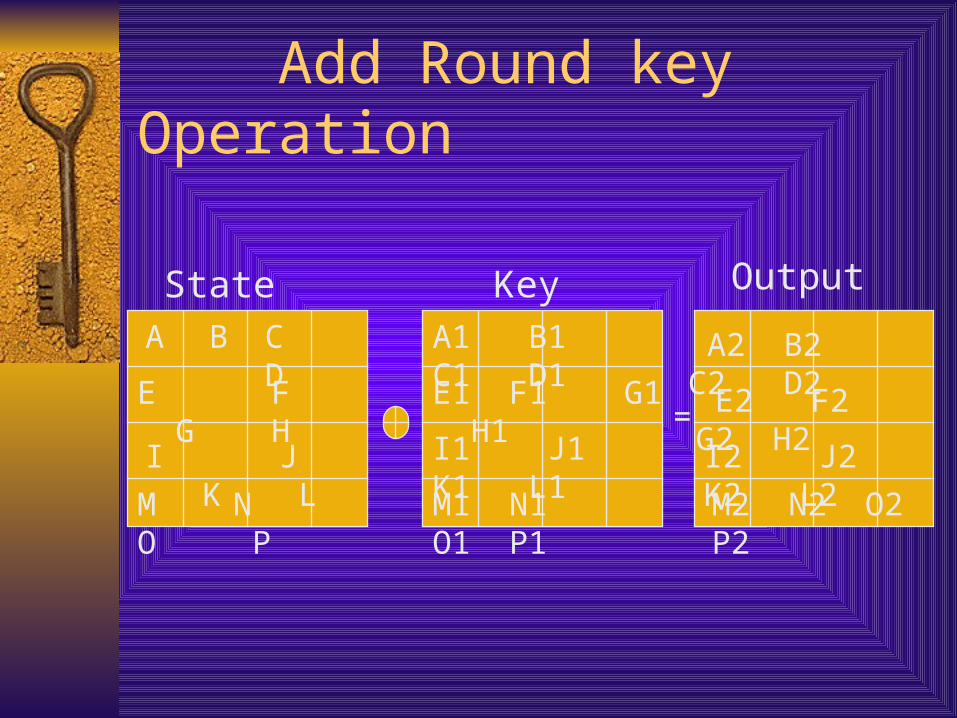
Add Round key Operation
A B C D
E F G H
I J K L
M N O P
A1 B1 C1 D1
E1 F1 G1 H1
I1 J1 K1 L1
M1 N1 O1 P1
A2 B2 C2 D2
E2 F2 G2 H2
I2 J2 K2 L2
M2 N2 O2 P2
=
State Key Output

State Diagram for Encryption Algorithm
S0
S2
S3 S1
Count=1
Count=2
Repeat until Count =10
Count=11
Roll back to S0

Future Work
Integrate all modules Synthesize all modules Power Estimation for the integrated system Repeat all previous steps for the Decryption
module


![KERALA GAZETTE tIcf Kkddv · 12th J UNE 2012] KERALA GAZETTE 822 11187 Aiyappan, P. Account Test -(L) – KSR, KFC 11197 Ajith Kumar, S. Criminal Judicial Test – The Indian Penal](https://img.pdfslide.us/doc/110x75/5e2067720c987531951e4986/kerala-gazette-ticf-12th-j-une-2012-kerala-gazette-822-11187-aiyappan-p-account.jpg)