Embed Size (px)
Citation preview
Copyright 2001, 2003, MD Ciletti 1
Advanced Digital Design with the Verilog HDL
M. D. Ciletti
Department
of Electrical and Computer Engineering
University of Colorado Colorado Springs, Colorado
Draft: Chap 7: Design and Synthesis of Datapath Controllers
REV 9/22/2003
Copyright 2000, 2002, 2003. These notes are solely for classroom use by the instructor. No part of these notes may be copied, reproduced, or distributed to a third party, including students, in any form without the written permission of the author.

Copyright 2001, 2003, MD Ciletti 2
Note to the instructor: These slides are provided solely for classroom use in academic institutions by the instructor using the text, Advance Digital Design with the Verilog HDL by Michael Ciletti, published by Prentice Hall. This material may not be used in off-campus instruction, resold, reproduced or generally distributed in the original or modified format for any purpose without the permission of the Author. This material may not be placed on any server or network, and is protected under all copyright laws, as they currently exist. I am providing these slides to you subject to your agreeing that you will not provide them to your students in hardcopy or electronic format or use them for off-campus instruction of any kind. Please email to me your agreement to these conditions. I will greatly appreciate your assisting me by calling to my attention any errors or any other revisions that would enhance the utility of these slides for classroom use.
Copyright 2001, 2003, MD Ciletti 3
Course Overview
• Review of combinational and sequential logic design • Modeling and verification with hardware description languages • Introduction to synthesis with HDLs • Programmable logic devices • State machines, datapath controllers, RISC CPU • Architectures and algorithms for computation and signal processing • Synchronization across clock domains • Timing analysis • Fault simulation and testing, JTAG, BIST
Copyright 2001, 2003, MD Ciletti 4
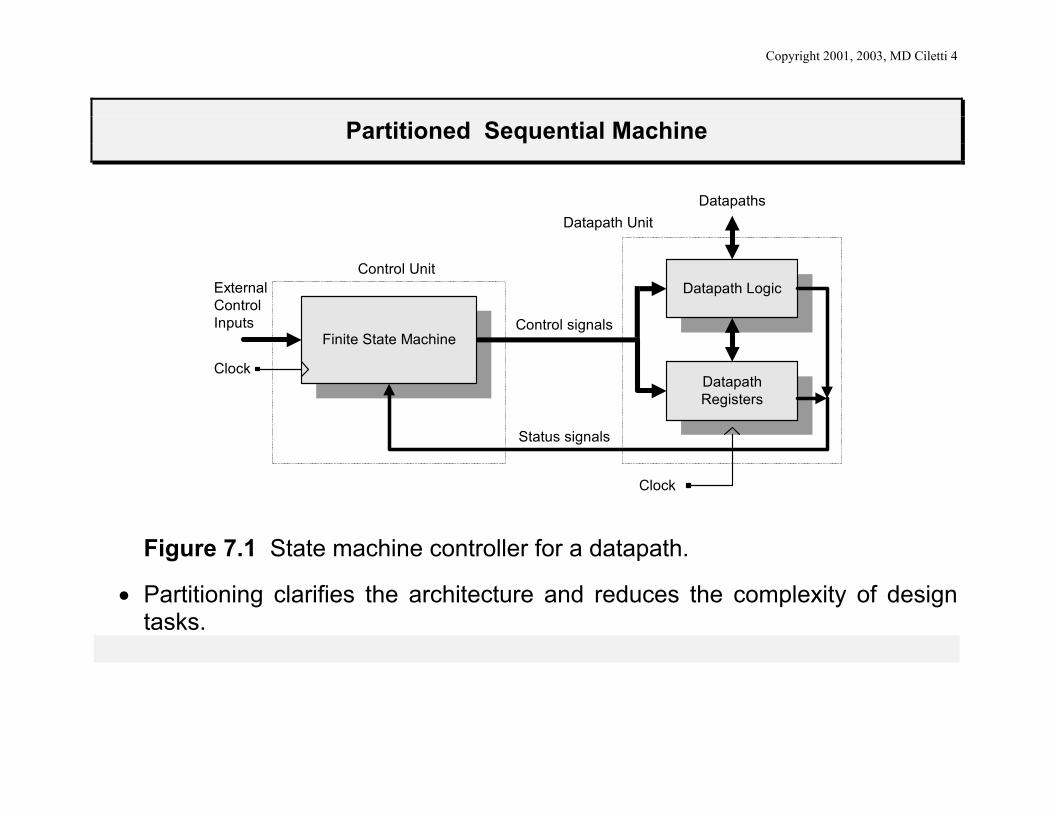
Partitioned Sequential Machine
Datapath Logic
DatapathRegisters
Finite State MachineControl signals
Clock
ExternalControlInputs
Datapaths
Clock
Status signals
Control Unit
Datapath Unit
Figure 7.1 State machine controller for a datapath.
• Partitioning clarifies the architecture and reduces the complexity of design tasks.
Copyright 2001, 2003, MD Ciletti 5
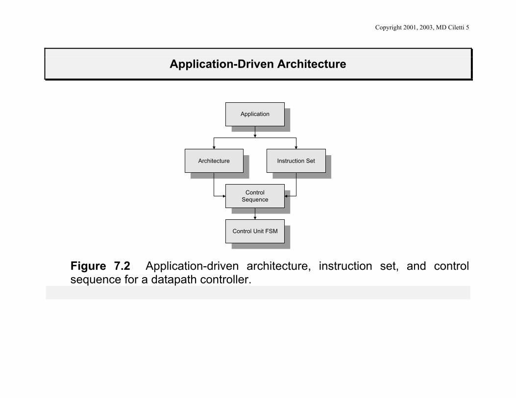
Application-Driven Architecture
Application
Architecture Instruction Set
ControlSequence
Control Unit FSM
Figure 7.2 Application-driven architecture, instruction set, and control sequence for a datapath controller.
Copyright 2001, 2003, MD Ciletti 6
Control Units for a Partitioned Sequential Machine
• Orchestrate, coordinate, and synchronize the operations of datapath units • Generate the signals that load, read and shift the contents of storage
registers • Fetch instructions and data from memory • Store data in memory • Steer signals through muxes • Control three-state devices • Control the operations of ALUs and other complex datapath units.
Copyright 2001, 2003, MD Ciletti 7
Sequential Machine
Common clock synchronizes the activities of the controller and datapath functional units Descriptions of functional units:
• Datapath units are commonly described by data flow graphs • Control units are commonly modeled by state transition graphs and/or
ASM charts for finite state machines.
Partitioned sequential machines can be modeled by a FSMD chart, a combined control-data flow graph, which expresses datapath operations in the context of a STG.
ASMD chart: links and ASM chart for a control unit to the operations of the datapath that it controls.
Copyright 2001, 2003, MD Ciletti 8
Design Example: Binary Counter
• Synchronous 4-bit binary counter • Incremented by a count of 1 at each active edge of the clock • Wrap count to 0 when the count reaches 11112.
Implicit machine: register transfer operation (count <= count + 1) conditionally, in every clock cycle, depending on enable Alternative Design: Partitioned machine: an architecture of separate datapath and control units, Functional elements of the architecture of the datapath unit: • 4-bit register to hold count, • mux that steers either count or the sum of count and 00012 to the input of the
register • a 4-bit adder to increment count • enable must be asserted for counting to occur • rst overrides all activity and drives the count to a value of 00002.
rst must be de-asserted and enable must be asserted for the machine to begin counting to begin and to continue counting.
Copyright 2001, 2003, MD Ciletti 9
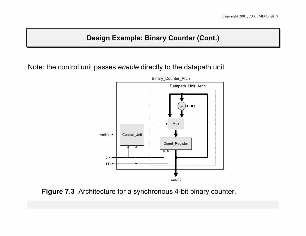
Design Example: Binary Counter (Cont.)
Note: the control unit passes enable directly to the datapath unit
Mux
Count_Register
+
Control_Unit
Datapath_Unit_Arch
enable
clkrst
count
1
Binary_Counter_Arch
Figure 7.3 Architecture for a synchronous 4-bit binary counter.
Copyright 2001, 2003, MD Ciletti 10
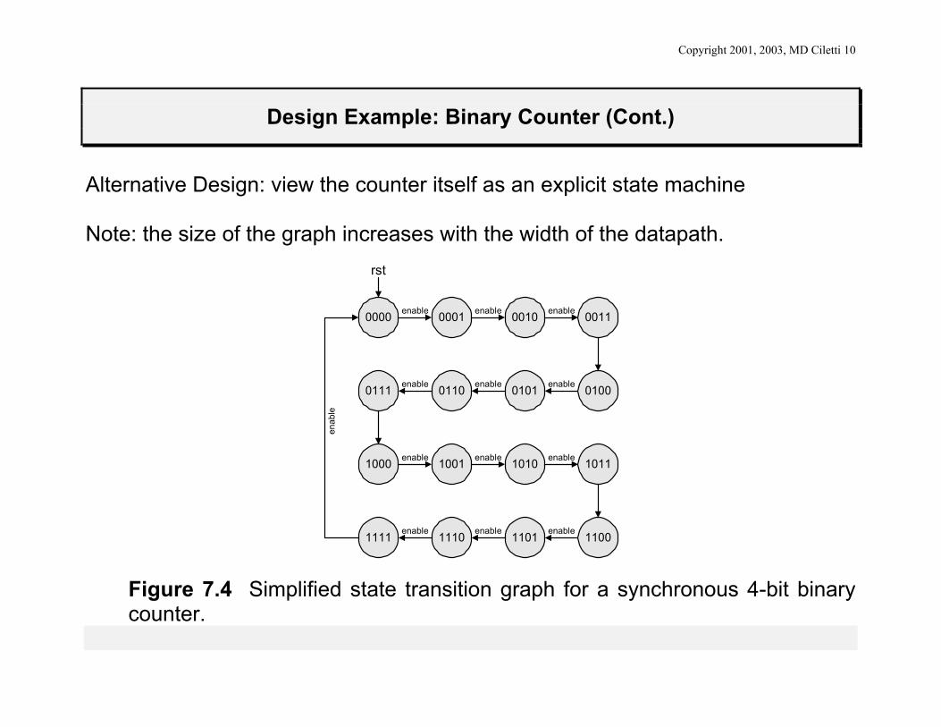
Design Example: Binary Counter (Cont.)
Alternative Design: view the counter itself as an explicit state machine Note: the size of the graph increases with the width of the datapath.
0000 0001 0010 0011
0111 0110 0101 0100
1000 1001 1010 1011
1111 1110 1101 1100
enab
le
enable enable
enableenableenable
enable enable enable
enableenableenable
rst
enable
Figure 7.4 Simplified state transition graph for a synchronous 4-bit binary counter.
Copyright 2001, 2003, MD Ciletti 11
Design Example: Binary Counter (Cont.)
Comparisons: • Implicit State Machine • Simplest description • Suppresses structural detail
• Partitioned Machine • Has the most structural detail • Has a simple controller • State of the datapath register does not influence the design
STG-based Design • Required a detailed STG • State machine as a state for each state of the counter • and lead to a state machine having 16 states
Copyright 2001, 2003, MD Ciletti 12
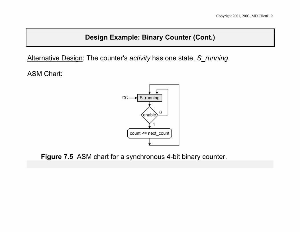
Design Example: Binary Counter (Cont.)
Alternative Design: The counter's activity has one state, S_running. ASM Chart:
S_running
enable 0
rst
count <= next_count
1
Figure 7.5 ASM chart for a synchronous 4-bit binary counter.
Copyright 2001, 2003, MD Ciletti 13
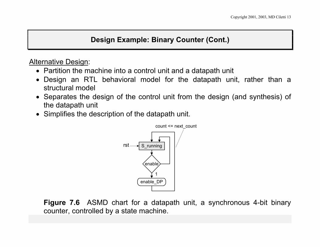
Design Example: Binary Counter (Cont.)
Alternative Design: • Partition the machine into a control unit and a datapath unit • Design an RTL behavioral model for the datapath unit, rather than a
structural model • Separates the design of the control unit from the design (and synthesis) of
the datapath unit • Simplifies the description of the datapath unit.
S_running
enable
rst
1
count <= next_count
enable_DP
Figure 7.6 ASMD chart for a datapath unit, a synchronous 4-bit binary counter, controlled by a state machine.
Copyright 2001, 2003, MD Ciletti 14
Design Example: Binary Counter (Cont.)
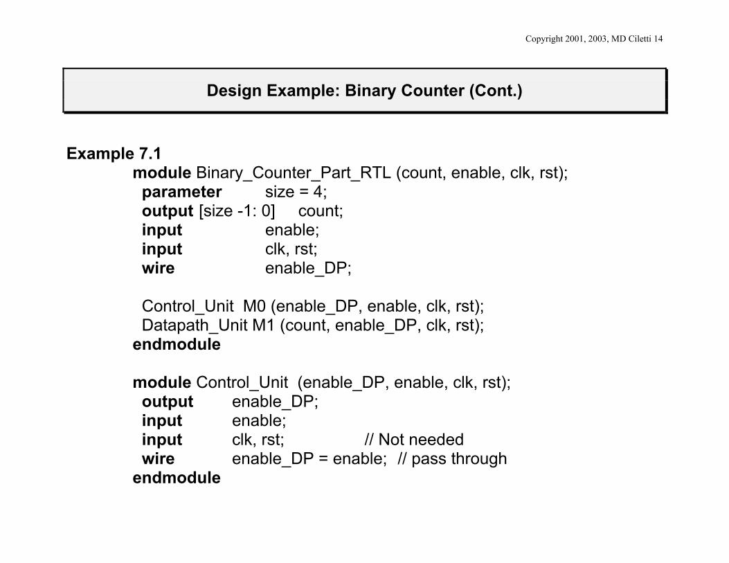
Example 7.1
module Binary_Counter_Part_RTL (count, enable, clk, rst); parameter size = 4; output [size -1: 0] count; input enable; input clk, rst; wire enable_DP; Control_Unit M0 (enable_DP, enable, clk, rst); Datapath_Unit M1 (count, enable_DP, clk, rst); endmodule module Control_Unit (enable_DP, enable, clk, rst); output enable_DP; input enable; input clk, rst; // Not needed wire enable_DP = enable; // pass through endmodule
Copyright 2001, 2003, MD Ciletti 15
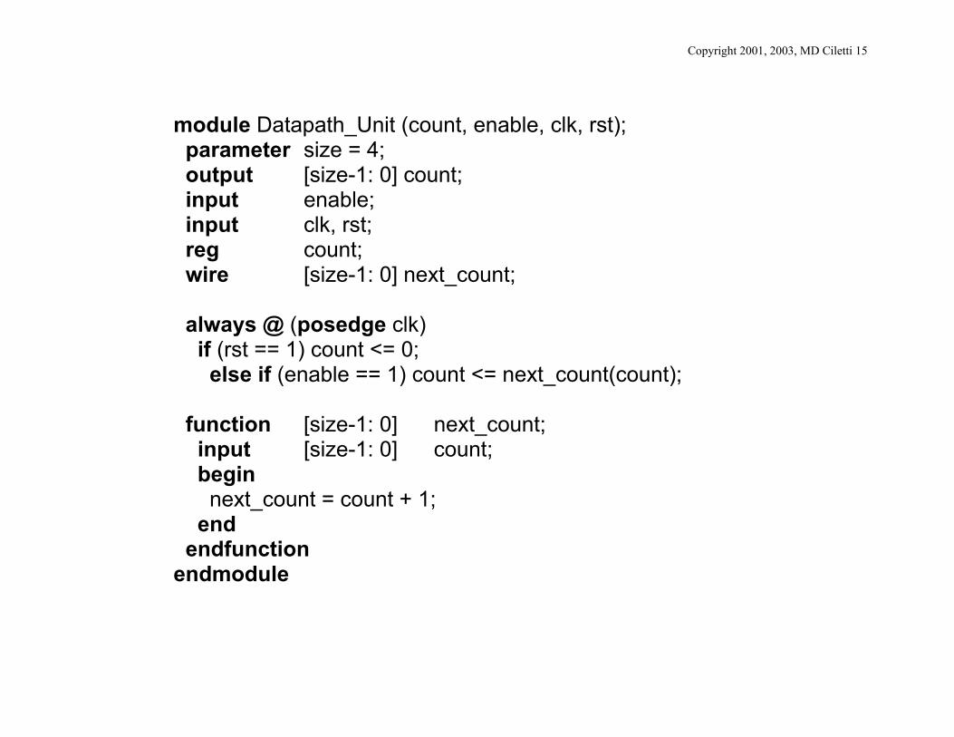
module Datapath_Unit (count, enable, clk, rst); parameter size = 4; output [size-1: 0] count; input enable; input clk, rst; reg count; wire [size-1: 0] next_count; always @ (posedge clk) if (rst == 1) count <= 0; else if (enable == 1) count <= next_count(count); function [size-1: 0] next_count; input [size-1: 0] count; begin next_count = count + 1; end endfunction endmodule
Copyright 2001, 2003, MD Ciletti 16
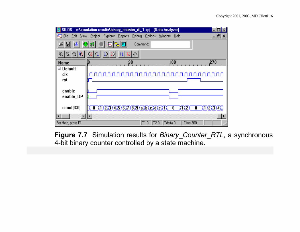
Figure 7.7 Simulation results for Binary_Counter_RTL, a synchronous 4-bit binary counter controlled by a state machine.
Copyright 2001, 2003, MD Ciletti 17
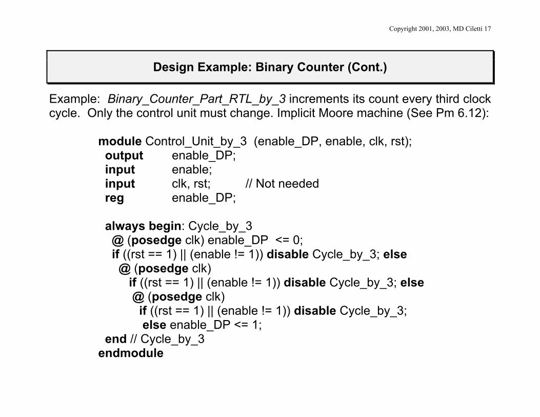
Design Example: Binary Counter (Cont.)
Example: Binary_Counter_Part_RTL_by_3 increments its count every third clock cycle. Only the control unit must change. Implicit Moore machine (See Pm 6.12):
module Control_Unit_by_3 (enable_DP, enable, clk, rst); output enable_DP; input enable; input clk, rst; // Not needed reg enable_DP; always begin: Cycle_by_3 @ (posedge clk) enable_DP <= 0; if ((rst == 1) || (enable != 1)) disable Cycle_by_3; else @ (posedge clk) if ((rst == 1) || (enable != 1)) disable Cycle_by_3; else @ (posedge clk) if ((rst == 1) || (enable != 1)) disable Cycle_by_3; else enable_DP <= 1; end // Cycle_by_3 endmodule
Copyright 2001, 2003, MD Ciletti 18
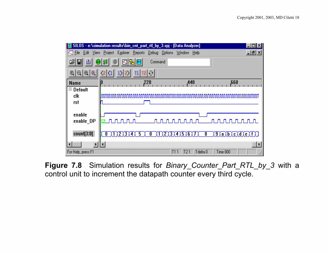
Figure 7.8 Simulation results for Binary_Counter_Part_RTL_by_3 with a control unit to increment the datapath counter every third cycle.
Copyright 2001, 2003, MD Ciletti 19
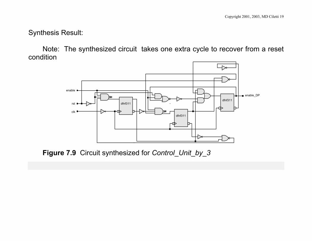
Synthesis Result: Note: The synthesized circuit takes one extra cycle to recover from a reset
condition
dfnf311
dfnf311
dfnf311
enable_DP
enable
rst
clk
Figure 7.9 Circuit synthesized for Control_Unit_by_3
Copyright 2001, 2003, MD Ciletti 20
RISC Stored Program Machine
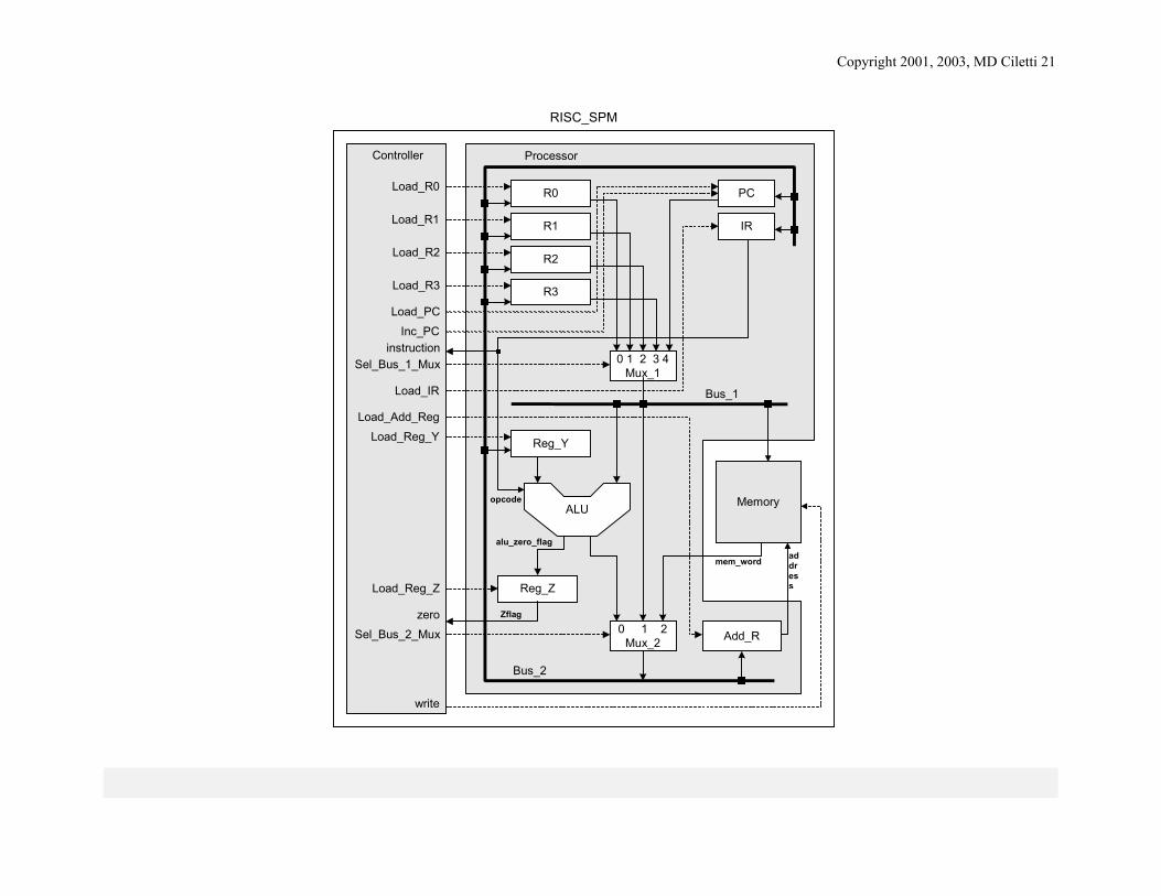
Copyright 2001, 2003, MD Ciletti 21
R0
R1
R2
R3
PC
0 1 2 3 4Mux_1
IR
Add_R
MemoryALU
Reg_Y
Reg_Z
0 1 2Mux_2
Bus_2
Bus_1
Controller
Load_Add_Reg
Load_PC
Inc_PC
Sel_Bus_1_Mux
Sel_Bus_2_Mux
Load_R0
Load_R1
Load_R2
Load_R3
Load_Reg_Y
Load_Reg_Z
opcode
Load_IR
write
Processor
RISC_SPM
address
alu_zero_flag
Zflagzero
instruction
mem_word
Copyright 2001, 2003, MD Ciletti 22
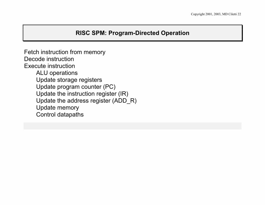
RISC SPM: Program-Directed Operation
Fetch instruction from memory Decode instruction Execute instruction
ALU operations Update storage registers Update program counter (PC) Update the instruction register (IR) Update the address register (ADD_R) Update memory Control datapaths
Copyright 2001, 2003, MD Ciletti 23
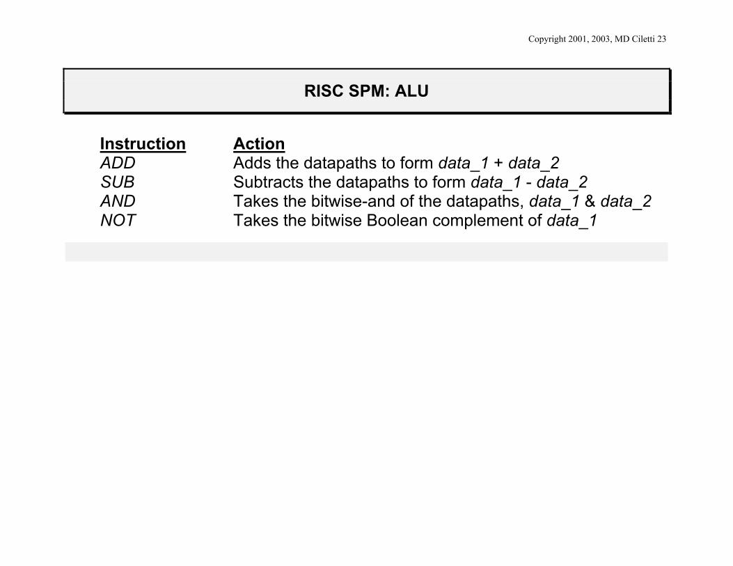
RISC SPM: ALU
Instruction Action ADD Adds the datapaths to form data_1 + data_2 SUB Subtracts the datapaths to form data_1 - data_2 AND Takes the bitwise-and of the datapaths, data_1 & data_2 NOT Takes the bitwise Boolean complement of data_1
Copyright 2001, 2003, MD Ciletti 24
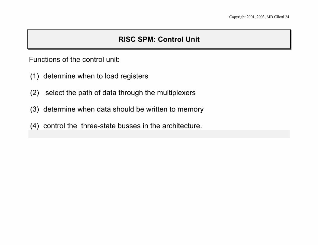
RISC SPM: Control Unit
Functions of the control unit: (1) determine when to load registers (2) select the path of data through the multiplexers (3) determine when data should be written to memory (4) control the three-state busses in the architecture.
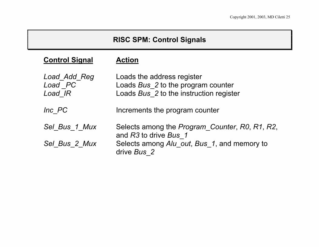
Copyright 2001, 2003, MD Ciletti 25
RISC SPM: Control Signals
Control Signal Action
Load_Add_Reg Loads the address register Load _PC Loads Bus_2 to the program counter Load_IR Loads Bus_2 to the instruction register Inc_PC Increments the program counter Sel_Bus_1_Mux Selects among the Program_Counter, R0, R1, R2,
and R3 to drive Bus_1 Sel_Bus_2_Mux Selects among Alu_out, Bus_1, and memory to
drive Bus_2
Copyright 2001, 2003, MD Ciletti 26
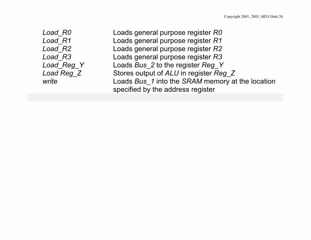
Load_R0 Loads general purpose register R0 Load_R1 Loads general purpose register R1 Load_R2 Loads general purpose register R2 Load_R3 Loads general purpose register R3 Load_Reg_Y Loads Bus_2 to the register Reg_Y Load Reg_Z Stores output of ALU in register Reg_Z write Loads Bus_1 into the SRAM memory at the location specified by the address register
Copyright 2001, 2003, MD Ciletti 27
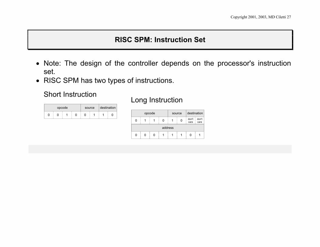
RISC SPM: Instruction Set
• Note: The design of the controller depends on the processor's instruction
set. • RISC SPM has two types of instructions.
Short Instruction
opcode source destination
0 0 1 0 0 1 1 0
Long Instruction
opcode source destination
address
0 1 1 0 1 0 don'tcare
don'tcare
0 0 0 1 1 1 0 1
Copyright 2001. 2003, MD Ciletti 28
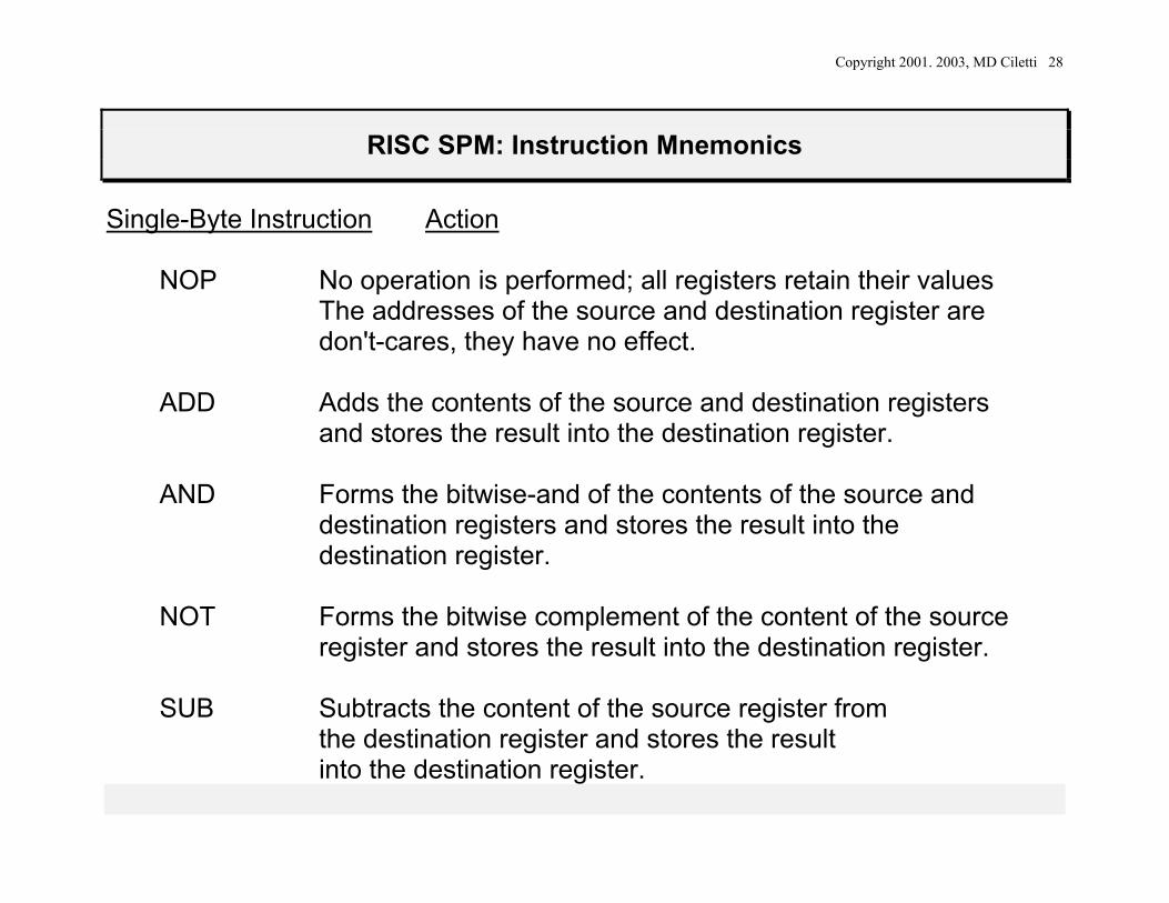
RISC SPM: Instruction Mnemonics
Single-Byte Instruction Action
NOP No operation is performed; all registers retain their values
The addresses of the source and destination register are don't-cares, they have no effect.
ADD Adds the contents of the source and destination registers and stores the result into the destination register.
AND Forms the bitwise-and of the contents of the source and destination registers and stores the result into the destination register.
NOT Forms the bitwise complement of the content of the source register and stores the result into the destination register.
SUB Subtracts the content of the source register from the destination register and stores the result into the destination register.
Copyright 2001. 2003, MD Ciletti 29
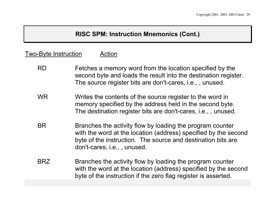
RISC SPM: Instruction Mnemonics (Cont.)
Two-Byte Instruction Action
RD Fetches a memory word from the location specified by the second byte and loads the result into the destination register.
The source register bits are don't-cares, i.e., , unused. WR Writes the contents of the source register to the word in memory specified by the address held in the second byte. The destination register bits are don't-cares, i.e., , unused. BR Branches the activity flow by loading the program counter
with the word at the location (address) specified by the second byte of the instruction. The source and destination bits are don't-cares, i.e., , unused.
BRZ Branches the activity flow by loading the program counter with the word at the location (address) specified by the second byte of the instruction if the zero flag register is asserted.
Copyright 2001. 2003, MD Ciletti 30
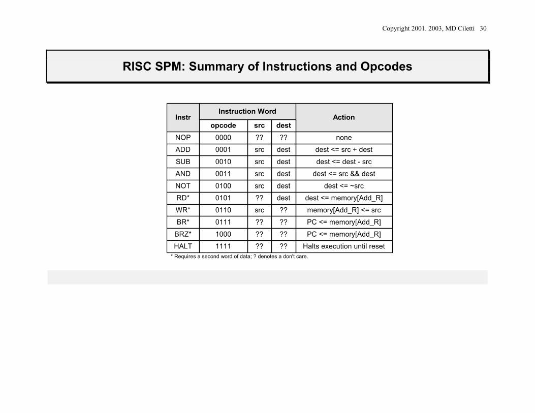
RISC SPM: Summary of Instructions and Opcodes
* Requires a second word of data; ? denotes a don't care.
opcodeNOP
ADD
AND
NOT
SUB
RD*
WR*
BR*
BRZ*
InstrInstruction Word
Action
none
dest <= src + dest
dest <= src && dest
dest <= ~src
dest <= dest - src
dest <= memory[Add_R]
PC <= memory[Add_R]
PC <= memory[Add_R]
memory[Add_R] <= src
src dest0000 ?? ??
0001 src dest
0011 src dest
0100 src dest
0010 src dest
0101 ?? dest
0110 src ??
0111 ?? ??
1000 ?? ??
HALT Halts execution until reset1111 ?? ??
Copyright 2001. 2003, MD Ciletti 31
RISC SPM: Program Counter
Holds the address of the next instruction to be executed. • When the external reset is asserted, the program counter is loaded with 0,
indicating that the bottom of memory holds the next instruction that will be fetched.
• Under the action of the clock, for single-cycle instructions, the instruction at
the address in the program counter is loaded into the instruction register and the program counter is incremented.
• An instruction decoder determines the resulting action on the datapaths and
the ALU. • A long instruction is held in two bytes, and an additional clock cycle is
required to execute the instruction. • In the second cycle of execution, the second byte is fetched from memory at
the address held in the program counter, then the instruction is completed.
Copyright 2001. 2003, MD Ciletti 32
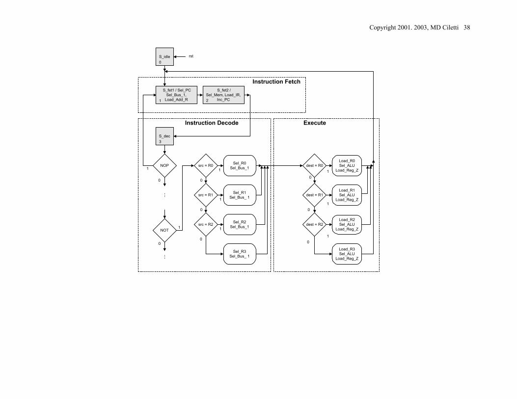
RISC SPM: Controller Design
Three phases of operation: fetch, decode, and execute. • Fetching: Retrieves an instruction from memory (2 clock cycles)
• Decoding: Decodes the instruction, manipulates datapaths, and loads
registers (1 cycle) • Execution generates the results of the instruction (0, 1, or 2 cycles)
Copyright 2001. 2003, MD Ciletti 33
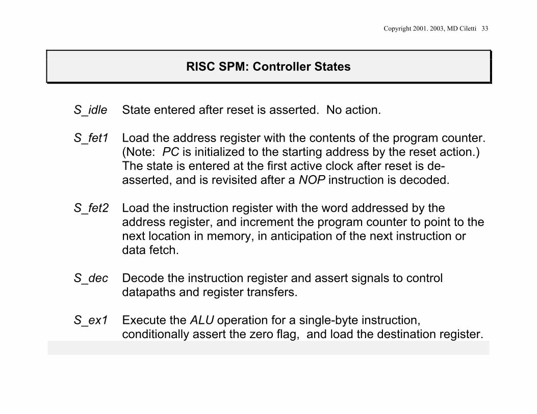
RISC SPM: Controller States
S_idle State entered after reset is asserted. No action.
S_fet1 Load the address register with the contents of the program counter. (Note: PC is initialized to the starting address by the reset action.) The state is entered at the first active clock after reset is de-asserted, and is revisited after a NOP instruction is decoded.
S_fet2 Load the instruction register with the word addressed by the
address register, and increment the program counter to point to the next location in memory, in anticipation of the next instruction or data fetch.
S_dec Decode the instruction register and assert signals to control
datapaths and register transfers. S_ex1 Execute the ALU operation for a single-byte instruction,
conditionally assert the zero flag, and load the destination register.
Copyright 2001. 2003, MD Ciletti 34
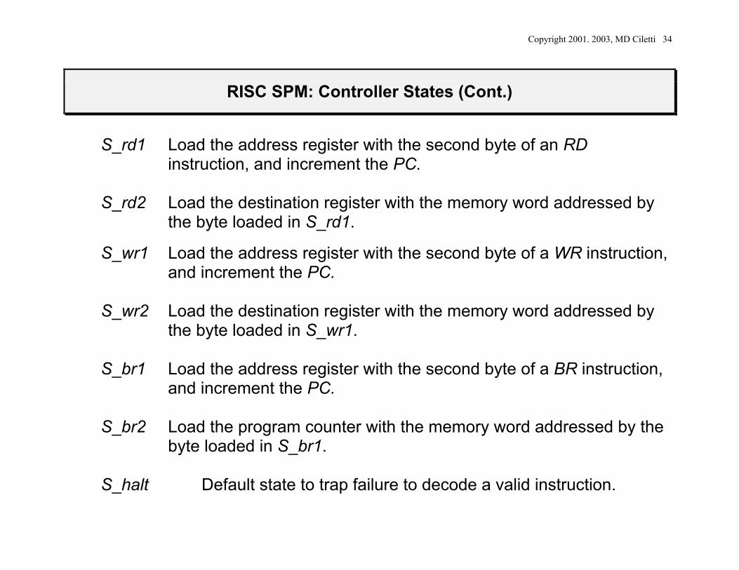
RISC SPM: Controller States (Cont.)
S_rd1 Load the address register with the second byte of an RD
instruction, and increment the PC. S_rd2 Load the destination register with the memory word addressed by
the byte loaded in S_rd1.
S_wr1 Load the address register with the second byte of a WR instruction, and increment the PC.
S_wr2 Load the destination register with the memory word addressed by
the byte loaded in S_wr1.
S_br1 Load the address register with the second byte of a BR instruction, and increment the PC.
S_br2 Load the program counter with the memory word addressed by the byte loaded in S_br1. S_halt Default state to trap failure to decode a valid instruction.
Copyright 2001. 2003, MD Ciletti 35
...
Copyright 2001. 2003, MD Ciletti 36
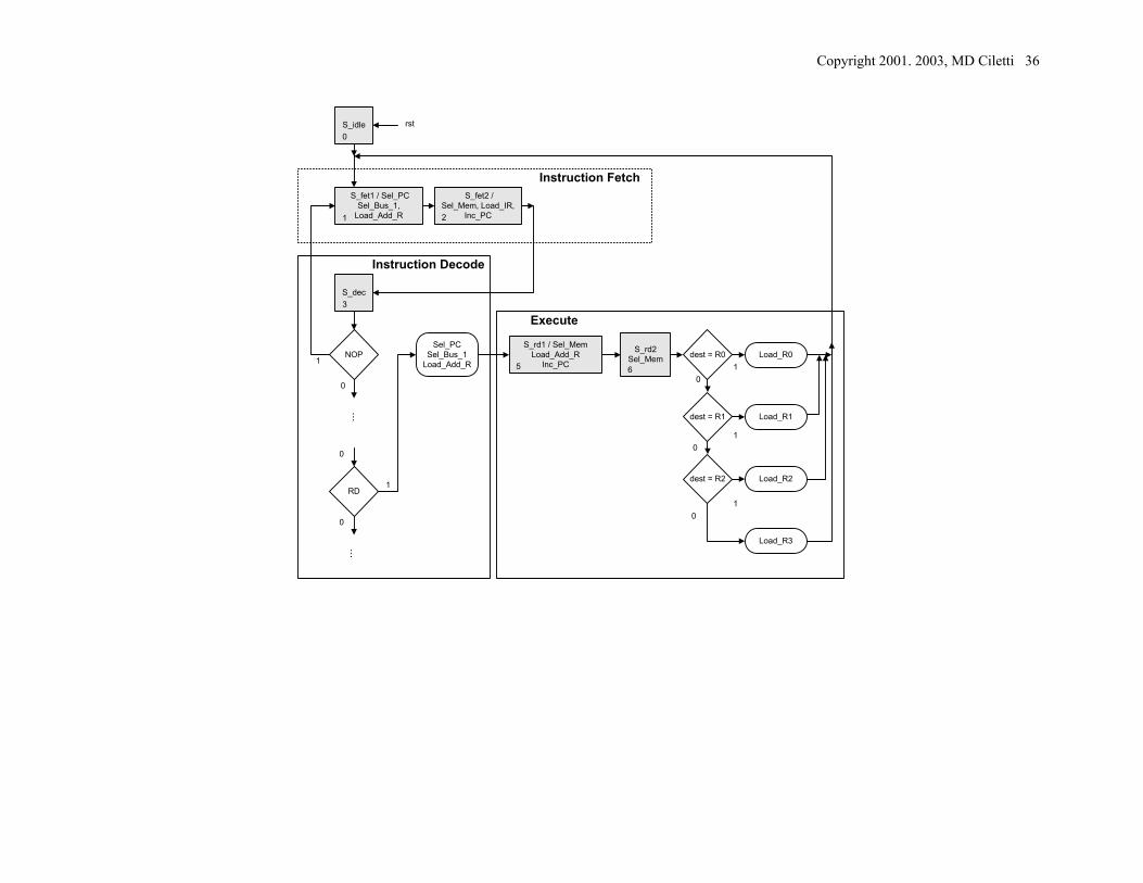
rst
NOP
0
Sel_PCSel_Bus_1
Load_Add_R1Load_R0
01
1
Load_R1
Load_R2
0
Load_R3
0
RD
0
1
0
...
dest = R0
dest = R1
dest = R2
1
S_idle
S_dec
S_rd1 / Sel_MemLoad_Add_R
Inc_PC
0
3
5
...
S_rd2Sel_Mem6
S_fet2 /Sel_Mem, Load_IR,
Inc_PC2
S_fet1 / Sel_PCSel_Bus_1,
Load_Add_R1
Instruction Fetch
Instruction Decode
Execute
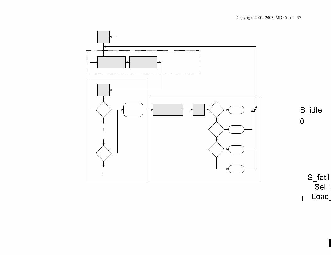
Copyright 2001. 2003, MD Ciletti 37
......
Copyright 2001. 2003, MD Ciletti 38
rst
NOP
0
Sel_R0Sel_Bus_11
0
1
1
Sel_R1Sel_Bus_ 1
Sel_R2Sel_Bus_1src = R2
0
1
Sel_R3Sel_Bus_ 1
0
Load_R0Sel_ALU
Load_Reg_Z
01
1
Load_R1Sel_ALU
Load_Reg_Z
Load_R2Sel_ALU
Load_Reg_Z
0
Load_R3Sel_ALU
Load_Reg_Z
0
NOT
0
1
...
src = R0
src = R1
dest = R0
dest = R1
dest = R2
1
S_idle
S_dec
0
3
...
S_fet2 /Sel_Mem, Load_IR,
Inc_PC2
S_fet1 / Sel_PCSel_Bus_1,
Load_Add_R1
Instruction Decode
Instruction Fetch
Execute
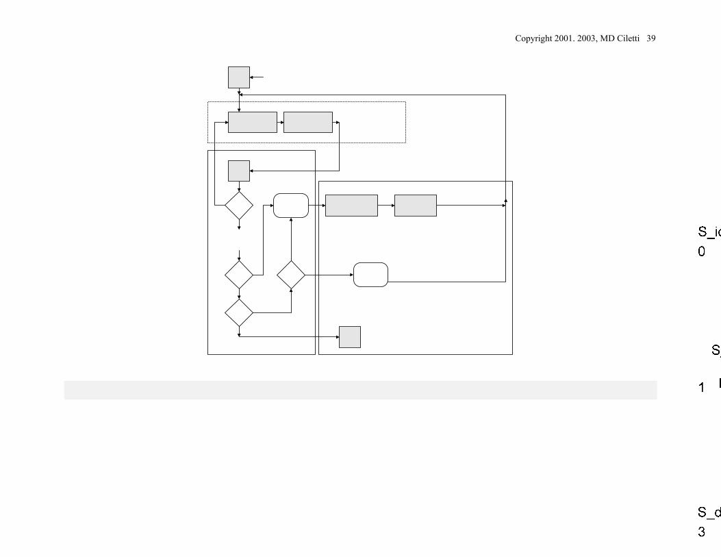
Copyright 2001. 2003, MD Ciletti 39
Copyright 2001. 2003, MD Ciletti 40
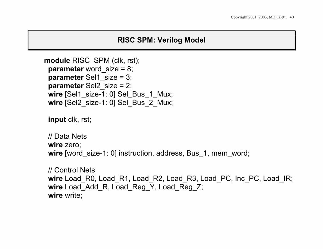
RISC SPM: Verilog Model
module RISC_SPM (clk, rst);
parameter word_size = 8; parameter Sel1_size = 3; parameter Sel2_size = 2; wire [Sel1_size-1: 0] Sel_Bus_1_Mux; wire [Sel2_size-1: 0] Sel_Bus_2_Mux; input clk, rst; // Data Nets wire zero; wire [word_size-1: 0] instruction, address, Bus_1, mem_word; // Control Nets wire Load_R0, Load_R1, Load_R2, Load_R3, Load_PC, Inc_PC, Load_IR; wire Load_Add_R, Load_Reg_Y, Load_Reg_Z; wire write;
Copyright 2001. 2003, MD Ciletti 41
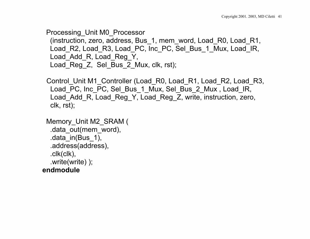
Processing_Unit M0_Processor (instruction, zero, address, Bus_1, mem_word, Load_R0, Load_R1, Load_R2, Load_R3, Load_PC, Inc_PC, Sel_Bus_1_Mux, Load_IR, Load_Add_R, Load_Reg_Y, Load_Reg_Z, Sel_Bus_2_Mux, clk, rst);
Control_Unit M1_Controller (Load_R0, Load_R1, Load_R2, Load_R3, Load_PC, Inc_PC, Sel_Bus_1_Mux, Sel_Bus_2_Mux , Load_IR, Load_Add_R, Load_Reg_Y, Load_Reg_Z, write, instruction, zero, clk, rst);
Memory_Unit M2_SRAM ( .data_out(mem_word), .data_in(Bus_1), .address(address), .clk(clk), .write(write) ); endmodule
Copyright 2001. 2003, MD Ciletti 42
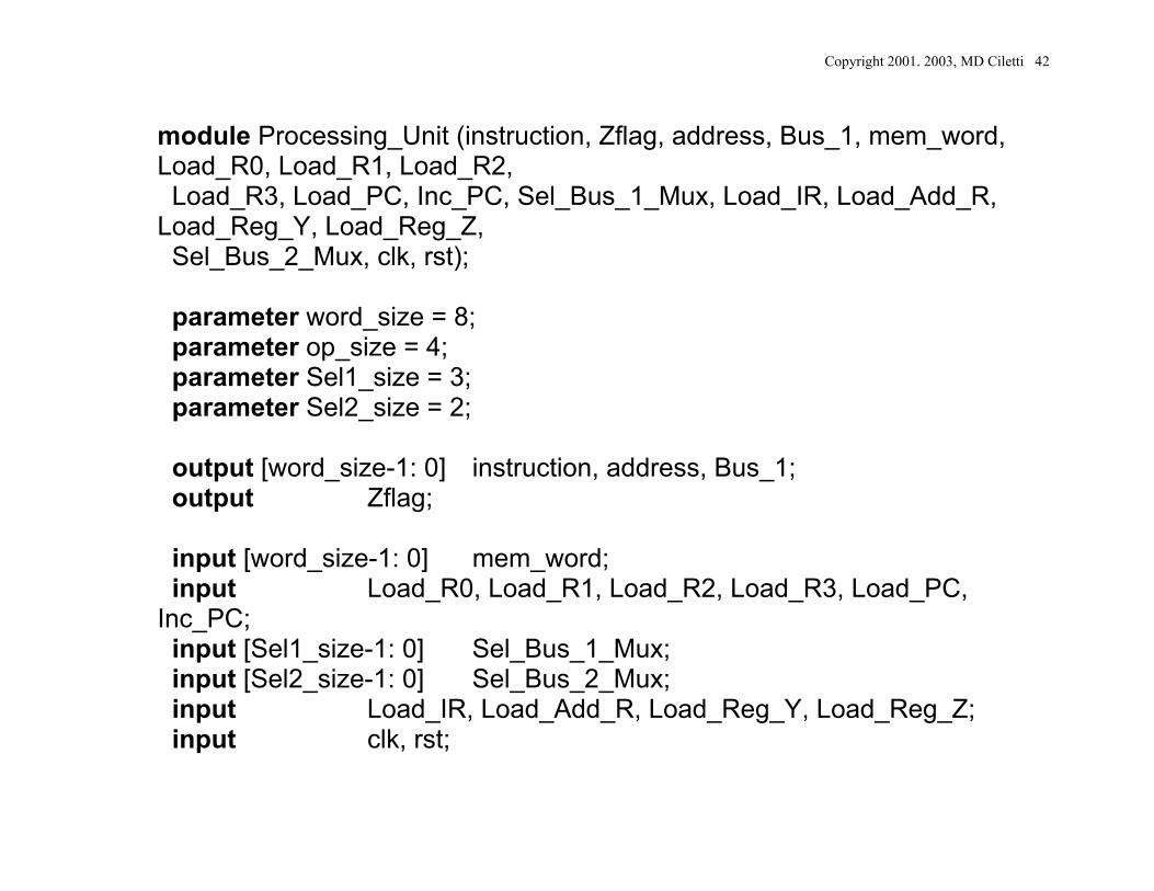
module Processing_Unit (instruction, Zflag, address, Bus_1, mem_word, Load_R0, Load_R1, Load_R2, Load_R3, Load_PC, Inc_PC, Sel_Bus_1_Mux, Load_IR, Load_Add_R, Load_Reg_Y, Load_Reg_Z, Sel_Bus_2_Mux, clk, rst); parameter word_size = 8; parameter op_size = 4; parameter Sel1_size = 3; parameter Sel2_size = 2; output [word_size-1: 0] instruction, address, Bus_1; output Zflag; input [word_size-1: 0] mem_word; input Load_R0, Load_R1, Load_R2, Load_R3, Load_PC, Inc_PC; input [Sel1_size-1: 0] Sel_Bus_1_Mux; input [Sel2_size-1: 0] Sel_Bus_2_Mux; input Load_IR, Load_Add_R, Load_Reg_Y, Load_Reg_Z; input clk, rst;
Copyright 2001. 2003, MD Ciletti 43
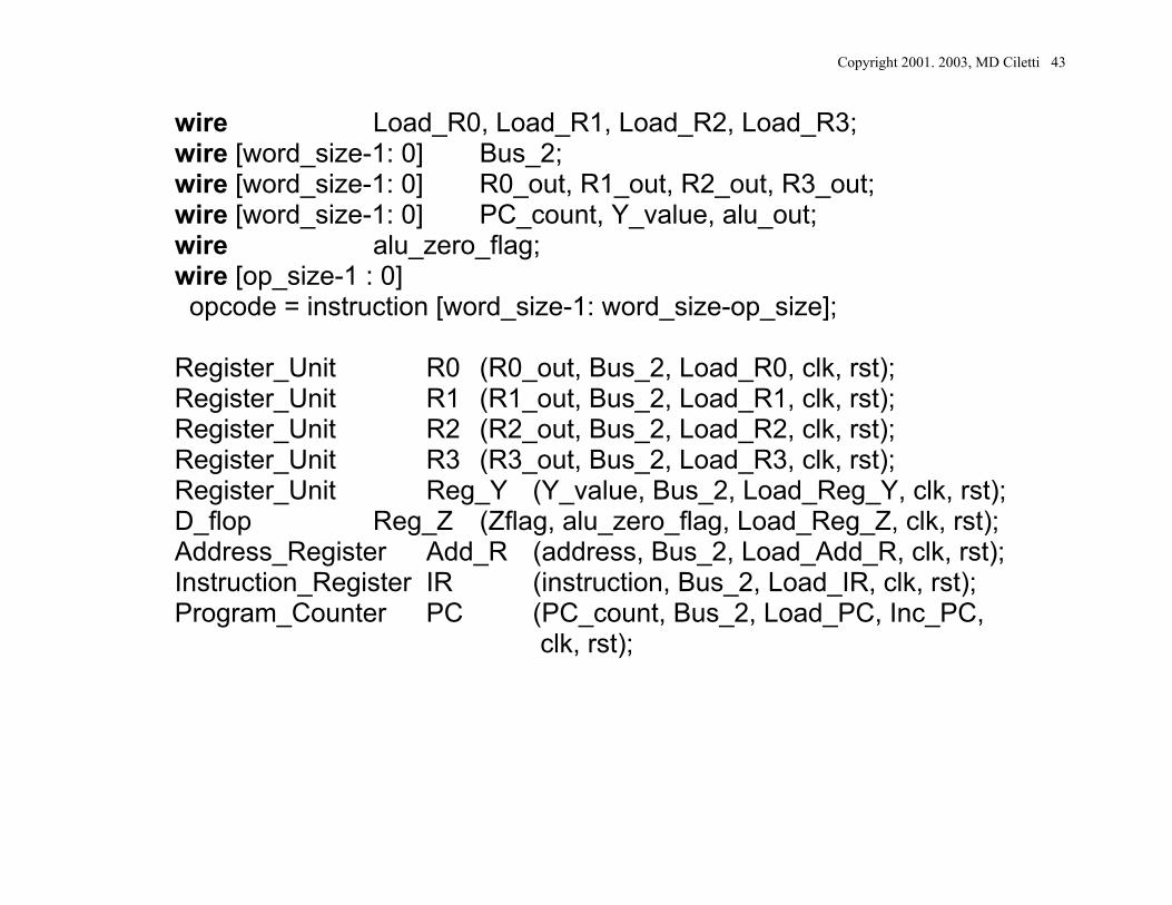
wire Load_R0, Load_R1, Load_R2, Load_R3; wire [word_size-1: 0] Bus_2; wire [word_size-1: 0] R0_out, R1_out, R2_out, R3_out; wire [word_size-1: 0] PC_count, Y_value, alu_out; wire alu_zero_flag; wire [op_size-1 : 0] opcode = instruction [word_size-1: word_size-op_size]; Register_Unit R0 (R0_out, Bus_2, Load_R0, clk, rst); Register_Unit R1 (R1_out, Bus_2, Load_R1, clk, rst); Register_Unit R2 (R2_out, Bus_2, Load_R2, clk, rst); Register_Unit R3 (R3_out, Bus_2, Load_R3, clk, rst); Register_Unit Reg_Y (Y_value, Bus_2, Load_Reg_Y, clk, rst); D_flop Reg_Z (Zflag, alu_zero_flag, Load_Reg_Z, clk, rst); Address_Register Add_R (address, Bus_2, Load_Add_R, clk, rst); Instruction_Register IR (instruction, Bus_2, Load_IR, clk, rst); Program_Counter PC (PC_count, Bus_2, Load_PC, Inc_PC,
clk, rst);
Copyright 2001. 2003, MD Ciletti 44
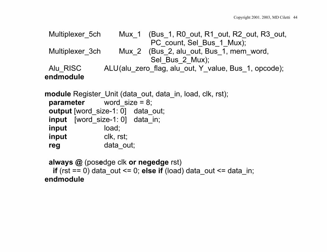
Multiplexer_5ch Mux_1 (Bus_1, R0_out, R1_out, R2_out, R3_out, PC_count, Sel_Bus_1_Mux);
Multiplexer_3ch Mux_2 (Bus_2, alu_out, Bus_1, mem_word, Sel_Bus_2_Mux);
Alu_RISC ALU (alu_zero_flag, alu_out, Y_value, Bus_1, opcode); endmodule module Register_Unit (data_out, data_in, load, clk, rst); parameter word_size = 8; output [word_size-1: 0] data_out; input [word_size-1: 0] data_in; input load; input clk, rst; reg data_out; always @ (posedge clk or negedge rst) if (rst == 0) data_out <= 0; else if (load) data_out <= data_in; endmodule
Copyright 2001. 2003, MD Ciletti 45
module D_flop (data_out, data_in, load, clk, rst); output data_out; input data_in; input load; input clk, rst; reg data_out; always @ (posedge clk or negedge rst) if (rst == 0) data_out <= 0; else if (load == 1)data_out <= data_in; endmodule module Address_Register (data_out, data_in, load, clk, rst); parameter word_size = 8; output [word_size-1: 0] data_out; input [word_size-1: 0] data_in; input load, clk, rst; reg data_out; always @ (posedge clk or negedge rst) if (rst == 0) data_out <= 0; else if (load) data_out <= data_in; endmodule
Copyright 2001. 2003, MD Ciletti 46
module Instruction_Register (data_out, data_in, load, clk, rst); parameter word_size = 8; output [word_size-1: 0] data_out; input [word_size-1: 0] data_in; input load; input clk, rst; reg data_out; always @ (posedge clk or negedge rst) if (rst == 0) data_out <= 0; else if (load) data_out <= data_in; endmodule module Program_Counter (count, data_in, Load_PC, Inc_PC, clk, rst); parameter word_size = 8; output [word_size-1: 0] count; input [word_size-1: 0] data_in; input Load_PC, Inc_PC; input clk, rst; reg count; always @ (posedge clk or negedge rst) if (rst == 0) count <= 0; else if (Load_PC) count <= data_in; else if (Inc_PC) count <= count +1; endmodule
Copyright 2001. 2003, MD Ciletti 47
module Multiplexer_5ch (mux_out, data_a, data_b, data_c, data_d, data_e, sel); parameter word_size = 8; output [word_size-1: 0] mux_out; input [word_size-1: 0] data_a, data_b, data_c, data_d, data_e; input [2: 0] sel; assign mux_out = (sel == 0) ? data_a: (sel == 1)
? data_b : (sel == 2) ? data_c: (sel == 3) ? data_d : (sel == 4) ? data_e : 'bx;
endmodule
Copyright 2001. 2003, MD Ciletti 48
module Multiplexer_3ch (mux_out, data_a, data_b, data_c, sel); parameter word_size = 8; output [word_size-1: 0] mux_out; input [word_size-1: 0] data_a, data_b, data_c; input [1: 0] sel; assign mux_out = (sel == 0) ? data_a: (sel == 1) ? data_b : (sel == 2) ? data_c: 'bx; endmodule
Copyright 2001. 2003, MD Ciletti 49
/*ALU Instruction Action ADD Adds the datapaths to form data_1 + data_2. SUB Subtracts the datapaths to form data_1 - data_2. AND Takes the bitwise-and of the datapaths, data_1 & data_2. NOT Takes the bitwise Boolean complement of data_1. */ // Note: the carries are ignored in this model. module Alu_RISC (alu_zero_flag, alu_out, data_1, data_2, sel); parameter word_size = 8; parameter op_size = 4; // Opcodes parameter NOP = 4'b0000; parameter ADD = 4'b0001; parameter SUB = 4'b0010; parameter AND = 4'b0011; parameter NOT = 4'b0100; parameter RD = 4'b0101; parameter WR = 4'b0110; parameter BR = 4'b0111; parameter BRZ = 4'b1000;
Copyright 2001. 2003, MD Ciletti 50
output alu_zero_flag; output [word_size-1: 0] alu_out; input [word_size-1: 0] data_1, data_2; input [op_size-1: 0] sel; reg alu_out; assign alu_zero_flag = ~|alu_out; always @ (sel or data_1 or data_2) case (sel) NOP: alu_out = 0; ADD: alu_out = data_1 + data_2; // Reg_Y + Bus_1 SUB: alu_out = data_2 - data_1; AND: alu_out = data_1 & data_2; NOT: alu_out = ~ data_2; // Gets data from Bus_1 default: alu_out = 0; endcase endmodule
Copyright 2001. 2003, MD Ciletti 51
module Control_Unit ( Load_R0, Load_R1, Load_R2, Load_R3, Load_PC, Inc_PC, Sel_Bus_1_Mux, Sel_Bus_2_Mux, Load_IR, Load_Add_R, Load_Reg_Y, Load_Reg_Z, write, instruction, zero, clk, rst); parameter word_size = 8, op_size = 4, state_size = 4; parameter src_size = 2, dest_size = 2, Sel1_size = 3, Sel2_size = 2; // State Codes parameter S_idle = 0, S_fet1 = 1, S_fet2 = 2, S_dec = 3; parameter S_ex1 = 4, S_rd1 = 5, S_rd2 = 6; parameter S_wr1 = 7, S_wr2 = 8, S_br1 = 9, S_br2 = 10, S_halt = 11; // Opcodes parameter NOP = 0, ADD = 1, SUB = 2, AND = 3, NOT = 4; parameter RD = 5, WR = 6, BR = 7, BRZ = 8; // Source and Destination Codes parameter R0 = 0, R1 = 1, R2 = 2, R3 = 3;
Copyright 2001. 2003, MD Ciletti 52
output Load_R0, Load_R1, Load_R2, Load_R3; output Load_PC, Inc_PC; output [Sel1_size-1: 0] Sel_Bus_1_Mux; output Load_IR, Load_Add_R; output Load_Reg_Y, Load_Reg_Z; output [Sel2_size-1: 0] Sel_Bus_2_Mux; output write; input [word_size-1: 0] instruction; input zero; input clk, rst; reg [state_size-1: 0] state, next_state; reg Load_R0, Load_R1, Load_R2, Load_R3, Load_PC, Inc_PC; reg Load_IR, Load_Add_R, Load_Reg_Y; reg Sel_ALU, Sel_Bus_1, Sel_Mem; reg Sel_R0, Sel_R1, Sel_R2, Sel_R3, Sel_PC; reg Load_Reg_Z, write; reg err_flag; wire [op_size-1: 0] opcode = instruction [word_size-1: word_size - op_size]; wire [src_size-1: 0] src = instruction [src_size + dest_size -1: dest_size]; wire [dest_size-1: 0] dest = instruction [dest_size -1: 0];
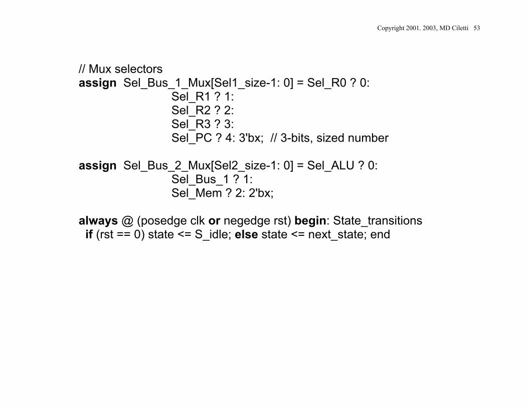
Copyright 2001. 2003, MD Ciletti 53
// Mux selectors assign Sel_Bus_1_Mux[Sel1_size-1: 0] = Sel_R0 ? 0: Sel_R1 ? 1: Sel_R2 ? 2: Sel_R3 ? 3: Sel_PC ? 4: 3'bx; // 3-bits, sized number assign Sel_Bus_2_Mux[Sel2_size-1: 0] = Sel_ALU ? 0: Sel_Bus_1 ? 1: Sel_Mem ? 2: 2'bx; always @ (posedge clk or negedge rst) begin: State_transitions if (rst == 0) state <= S_idle; else state <= next_state; end
Copyright 2001. 2003, MD Ciletti 54
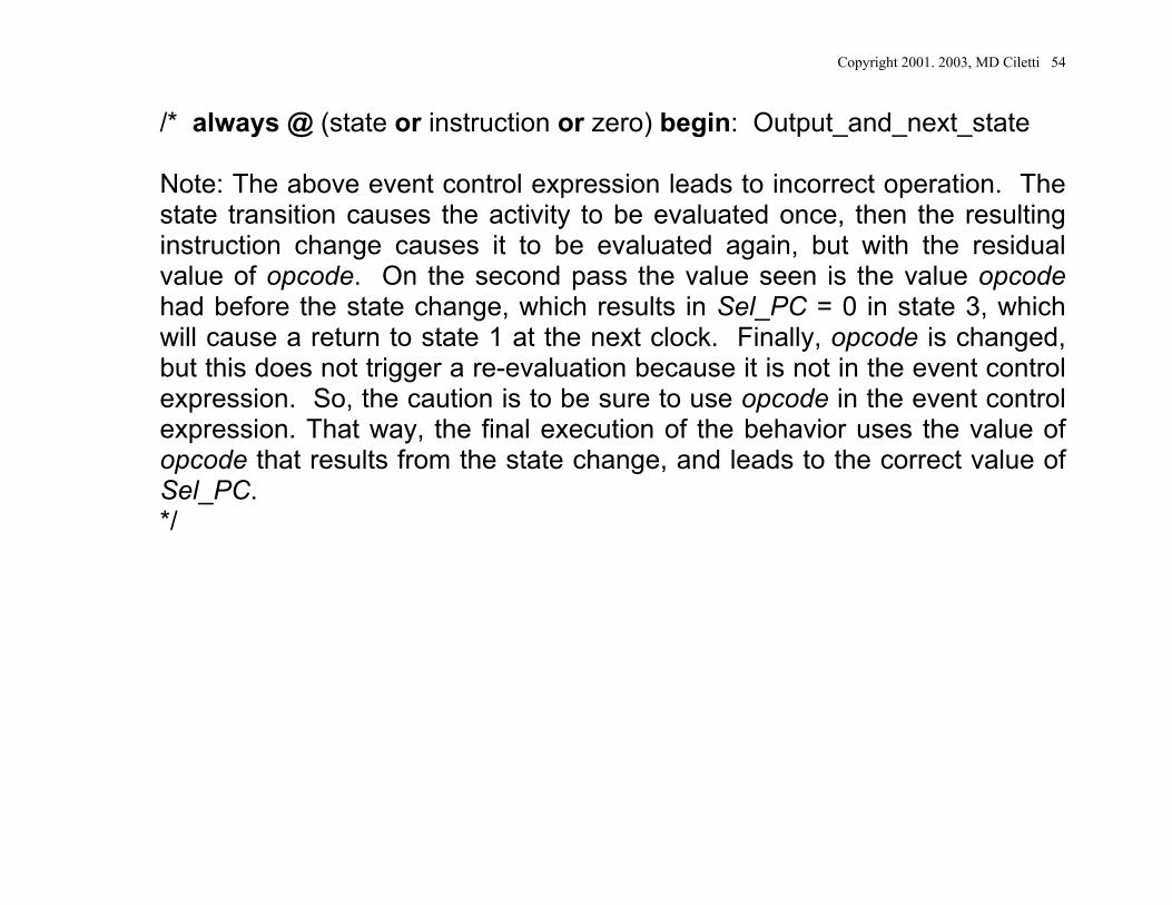
/* always @ (state or instruction or zero) begin: Output_and_next_state Note: The above event control expression leads to incorrect operation. The state transition causes the activity to be evaluated once, then the resulting instruction change causes it to be evaluated again, but with the residual value of opcode. On the second pass the value seen is the value opcode had before the state change, which results in Sel_PC = 0 in state 3, which will cause a return to state 1 at the next clock. Finally, opcode is changed, but this does not trigger a re-evaluation because it is not in the event control expression. So, the caution is to be sure to use opcode in the event control expression. That way, the final execution of the behavior uses the value of opcode that results from the state change, and leads to the correct value of Sel_PC. */
Copyright 2001. 2003, MD Ciletti 55
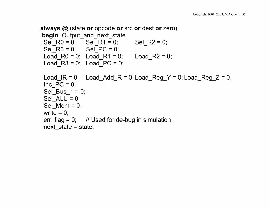
always @ (state or opcode or src or dest or zero) begin: Output_and_next_state Sel_R0 = 0; Sel_R1 = 0; Sel_R2 = 0; Sel_R3 = 0; Sel_PC = 0; Load_R0 = 0; Load_R1 = 0; Load_R2 = 0; Load_R3 = 0; Load_PC = 0; Load_IR = 0; Load_Add_R = 0; Load_Reg_Y = 0; Load_Reg_Z = 0; Inc_PC = 0; Sel_Bus_1 = 0; Sel_ALU = 0; Sel_Mem = 0; write = 0; err_flag = 0; // Used for de-bug in simulation next_state = state;
Copyright 2001. 2003, MD Ciletti 56
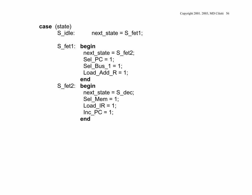
case (state) S_idle: next_state = S_fet1;
S_fet1: begin
next_state = S_fet2; Sel_PC = 1; Sel_Bus_1 = 1; Load_Add_R = 1; end S_fet2: begin
next_state = S_dec; Sel_Mem = 1;
Load_IR = 1; Inc_PC = 1; end
Copyright 2001. 2003, MD Ciletti 57
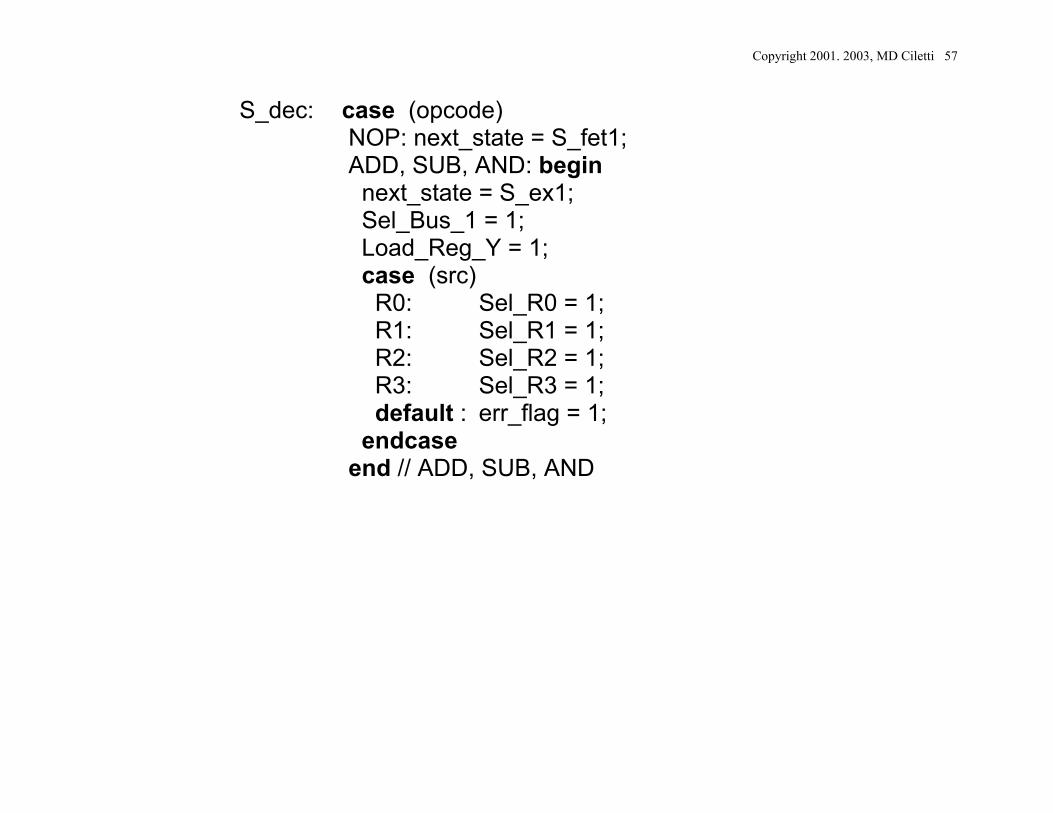
S_dec: case (opcode) NOP: next_state = S_fet1; ADD, SUB, AND: begin next_state = S_ex1; Sel_Bus_1 = 1; Load_Reg_Y = 1; case (src) R0: Sel_R0 = 1; R1: Sel_R1 = 1; R2: Sel_R2 = 1; R3: Sel_R3 = 1; default : err_flag = 1; endcase
end // ADD, SUB, AND
Copyright 2001. 2003, MD Ciletti 58
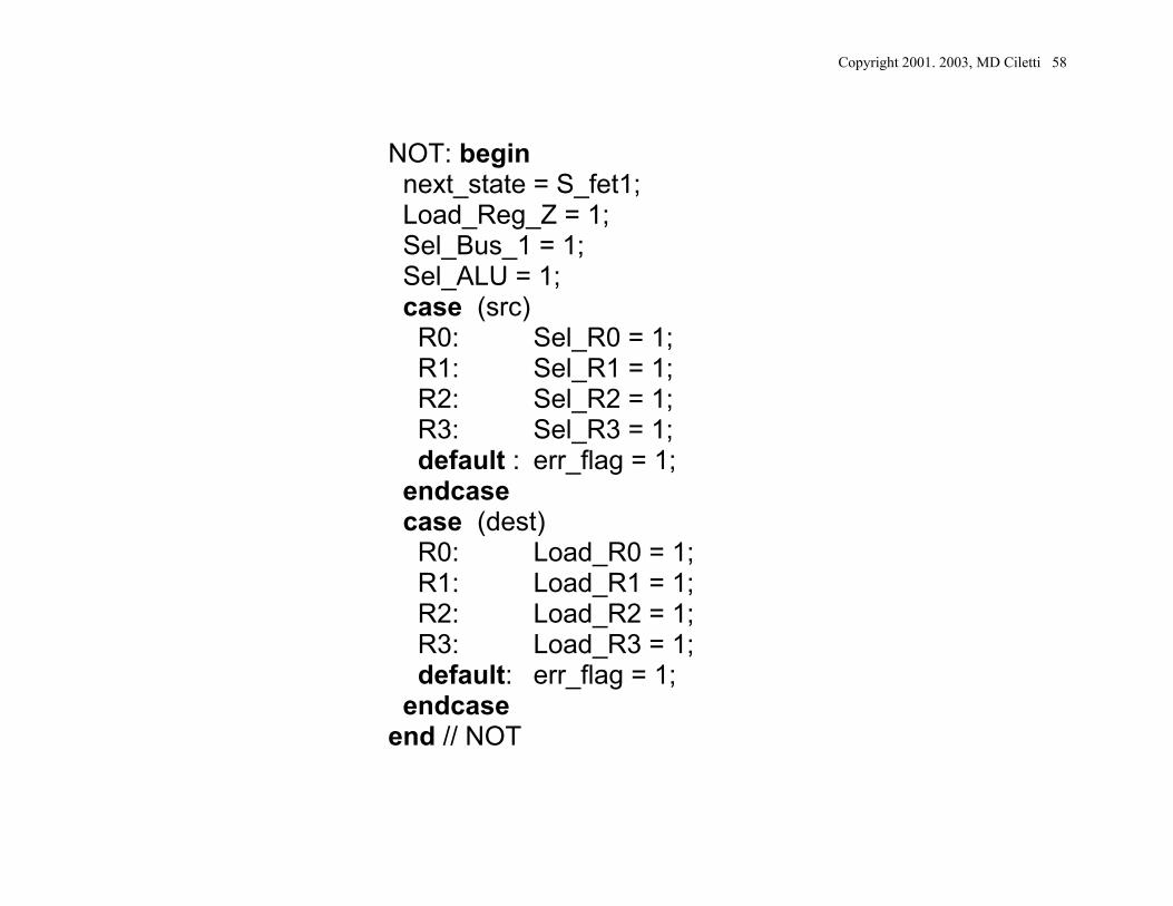
NOT: begin next_state = S_fet1; Load_Reg_Z = 1; Sel_Bus_1 = 1; Sel_ALU = 1; case (src) R0: Sel_R0 = 1; R1: Sel_R1 = 1; R2: Sel_R2 = 1; R3: Sel_R3 = 1; default : err_flag = 1; endcase case (dest) R0: Load_R0 = 1; R1: Load_R1 = 1; R2: Load_R2 = 1; R3: Load_R3 = 1; default: err_flag = 1; endcase
end // NOT
Copyright 2001. 2003, MD Ciletti 59
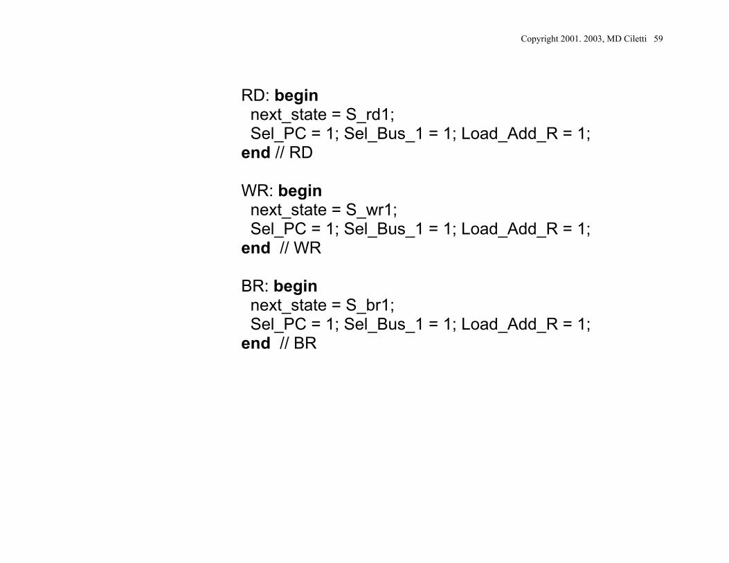
RD: begin
next_state = S_rd1; Sel_PC = 1; Sel_Bus_1 = 1; Load_Add_R = 1;
end // RD WR: begin next_state = S_wr1; Sel_PC = 1; Sel_Bus_1 = 1; Load_Add_R = 1;
end // WR BR: begin next_state = S_br1;
Sel_PC = 1; Sel_Bus_1 = 1; Load_Add_R = 1; end // BR
Copyright 2001. 2003, MD Ciletti 60
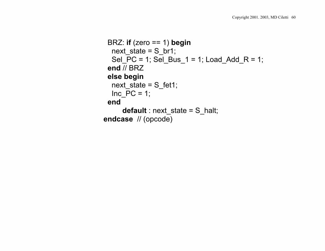
BRZ: if (zero == 1) begin next_state = S_br1;
Sel_PC = 1; Sel_Bus_1 = 1; Load_Add_R = 1; end // BRZ else begin
next_state = S_fet1; Inc_PC = 1; end
default : next_state = S_halt; endcase // (opcode)
Copyright 2001. 2003, MD Ciletti 61
S_ex1: begin next_state = S_fet1; Load_Reg_Z = 1; Sel_ALU = 1; case (dest) R0: begin Sel_R0 = 1; Load_R0 = 1; end R1: begin Sel_R1 = 1; Load_R1 = 1; end R2: begin Sel_R2 = 1; Load_R2 = 1; end R3: begin Sel_R3 = 1; Load_R3 = 1; end default : err_flag = 1; endcase end S_rd1: begin
next_state = S_rd2; Sel_Mem = 1; Load_Add_R = 1; Inc_PC = 1; end
Copyright 2001. 2003, MD Ciletti 62
S_wr1: begin next_state = S_wr2; Sel_Mem = 1; Load_Add_R = 1; Inc_PC = 1; end S_rd2: begin next_state = S_fet1; Sel_Mem = 1; case (dest) R0: Load_R0 = 1; R1: Load_R1 = 1; R2: Load_R2 = 1; R3: Load_R3 = 1; default : err_flag = 1; endcase end
Copyright 2001. 2003, MD Ciletti 63
S_wr2: begin next_state = S_fet1; write = 1; case (src) R0: Sel_R0 = 1; R1: Sel_R1 = 1; R2: Sel_R2 = 1; R3: Sel_R3 = 1; default : err_flag = 1; endcase end S_br1: begin next_state = S_br2; Sel_Mem = 1; Load_Add_R = 1; end S_br2: begin next_state = S_fet1; Sel_Mem = 1; Load_PC = 1; end S_halt: next_state = S_halt; default: next_state = S_idle; endcase end endmodule
Copyright 2001. 2003, MD Ciletti 64
module Memory_Unit (data_out, data_in, address, clk, write); parameter word_size = 8; parameter memory_size = 256; output [word_size-1: 0] data_out; input [word_size-1: 0] data_in; input [word_size-1: 0] address; input clk, write; reg [word_size-1: 0] memory [memory_size-1: 0]; assign data_out = memory[address]; always @ (posedge clk) if (write) memory[address] = data_in; endmodule
Copyright 2001. 2003, MD Ciletti 65
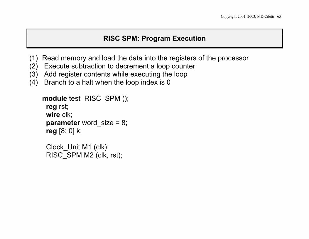
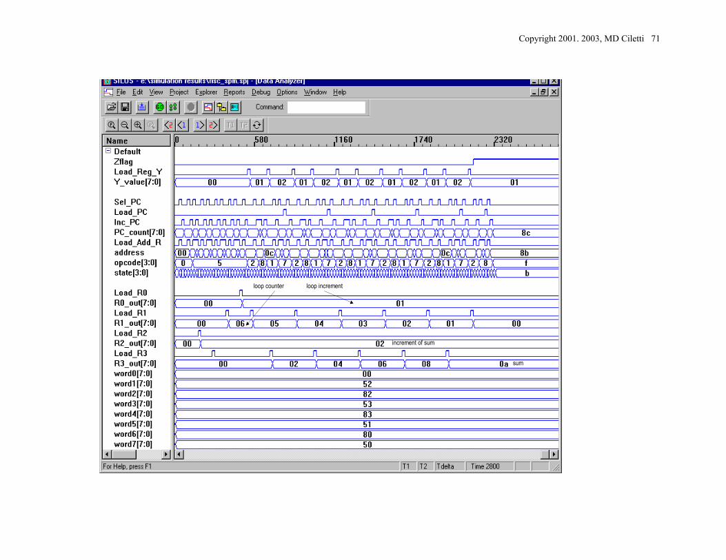
RISC SPM: Program Execution
(1) Read memory and load the data into the registers of the processor (2) Execute subtraction to decrement a loop counter (3) Add register contents while executing the loop (4) Branch to a halt when the loop index is 0
module test_RISC_SPM (); reg rst; wire clk; parameter word_size = 8; reg [8: 0] k; Clock_Unit M1 (clk); RISC_SPM M2 (clk, rst);
Copyright 2001. 2003, MD Ciletti 66
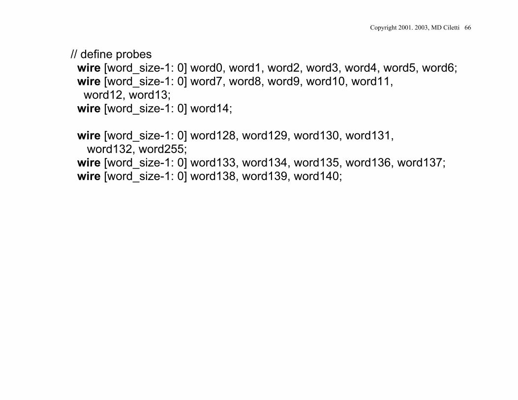
// define probes wire [word_size-1: 0] word0, word1, word2, word3, word4, word5, word6; wire [word_size-1: 0] word7, word8, word9, word10, word11, word12, word13; wire [word_size-1: 0] word14; wire [word_size-1: 0] word128, word129, word130, word131, word132, word255; wire [word_size-1: 0] word133, word134, word135, word136, word137; wire [word_size-1: 0] word138, word139, word140;
Copyright 2001. 2003, MD Ciletti 67
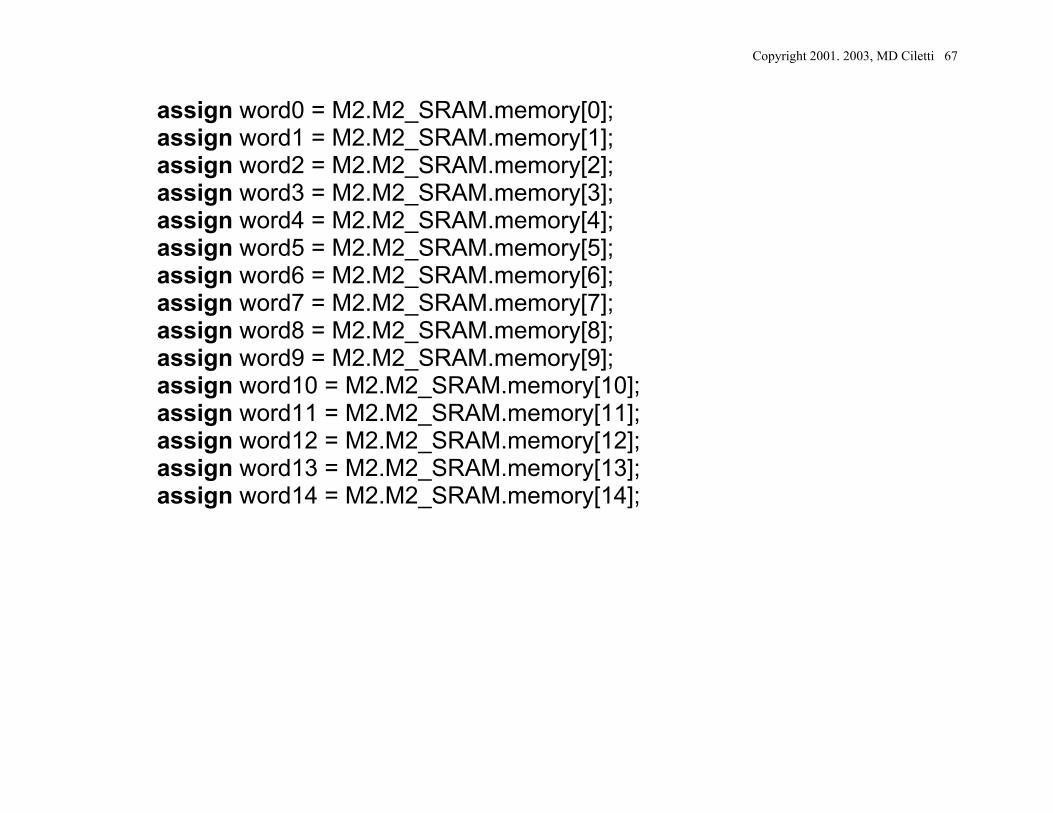
assign word0 = M2.M2_SRAM.memory[0]; assign word1 = M2.M2_SRAM.memory[1]; assign word2 = M2.M2_SRAM.memory[2]; assign word3 = M2.M2_SRAM.memory[3]; assign word4 = M2.M2_SRAM.memory[4]; assign word5 = M2.M2_SRAM.memory[5]; assign word6 = M2.M2_SRAM.memory[6]; assign word7 = M2.M2_SRAM.memory[7]; assign word8 = M2.M2_SRAM.memory[8]; assign word9 = M2.M2_SRAM.memory[9]; assign word10 = M2.M2_SRAM.memory[10]; assign word11 = M2.M2_SRAM.memory[11]; assign word12 = M2.M2_SRAM.memory[12]; assign word13 = M2.M2_SRAM.memory[13]; assign word14 = M2.M2_SRAM.memory[14];
Copyright 2001. 2003, MD Ciletti 68
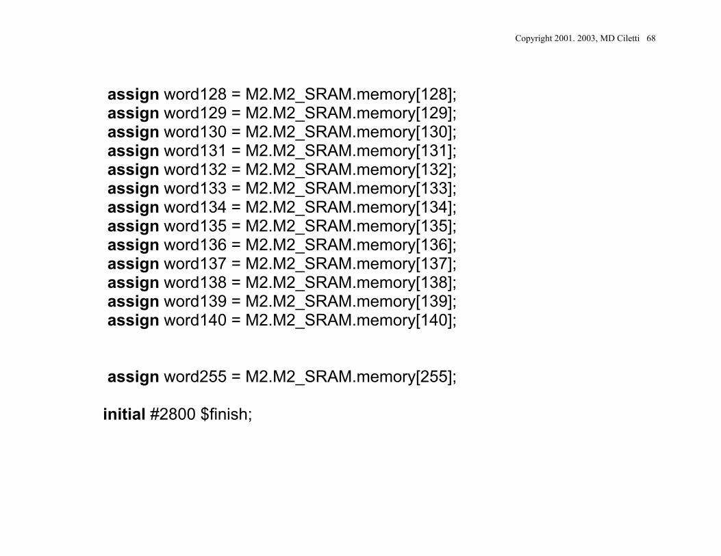
assign word128 = M2.M2_SRAM.memory[128]; assign word129 = M2.M2_SRAM.memory[129]; assign word130 = M2.M2_SRAM.memory[130]; assign word131 = M2.M2_SRAM.memory[131]; assign word132 = M2.M2_SRAM.memory[132]; assign word133 = M2.M2_SRAM.memory[133]; assign word134 = M2.M2_SRAM.memory[134]; assign word135 = M2.M2_SRAM.memory[135]; assign word136 = M2.M2_SRAM.memory[136]; assign word137 = M2.M2_SRAM.memory[137]; assign word138 = M2.M2_SRAM.memory[138]; assign word139 = M2.M2_SRAM.memory[139]; assign word140 = M2.M2_SRAM.memory[140]; assign word255 = M2.M2_SRAM.memory[255]; initial #2800 $finish;
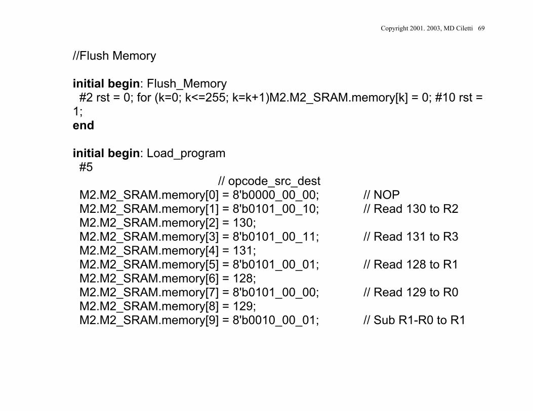
Copyright 2001. 2003, MD Ciletti 69
//Flush Memory initial begin: Flush_Memory #2 rst = 0; for (k=0; k<=255; k=k+1)M2.M2_SRAM.memory[k] = 0; #10 rst = 1; end initial begin: Load_program #5 // opcode_src_dest M2.M2_SRAM.memory[0] = 8'b0000_00_00; // NOP M2.M2_SRAM.memory[1] = 8'b0101_00_10; // Read 130 to R2 M2.M2_SRAM.memory[2] = 130; M2.M2_SRAM.memory[3] = 8'b0101_00_11; // Read 131 to R3 M2.M2_SRAM.memory[4] = 131; M2.M2_SRAM.memory[5] = 8'b0101_00_01; // Read 128 to R1 M2.M2_SRAM.memory[6] = 128; M2.M2_SRAM.memory[7] = 8'b0101_00_00; // Read 129 to R0 M2.M2_SRAM.memory[8] = 129; M2.M2_SRAM.memory[9] = 8'b0010_00_01; // Sub R1-R0 to R1
Copyright 2001. 2003, MD Ciletti 70
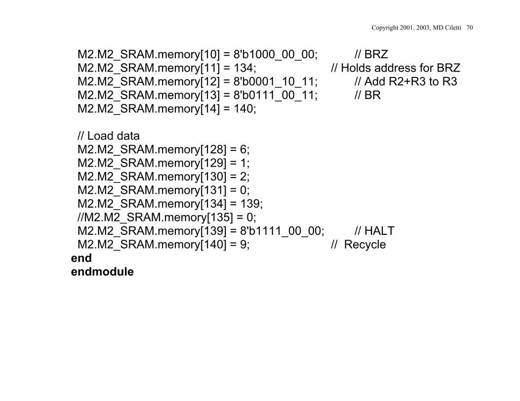
M2.M2_SRAM.memory[10] = 8'b1000_00_00; // BRZ M2.M2_SRAM.memory[11] = 134; // Holds address for BRZ M2.M2_SRAM.memory[12] = 8'b0001_10_11; // Add R2+R3 to R3 M2.M2_SRAM.memory[13] = 8'b0111_00_11; // BR M2.M2_SRAM.memory[14] = 140; // Load data M2.M2_SRAM.memory[128] = 6; M2.M2_SRAM.memory[129] = 1; M2.M2_SRAM.memory[130] = 2; M2.M2_SRAM.memory[131] = 0; M2.M2_SRAM.memory[134] = 139; //M2.M2_SRAM.memory[135] = 0; M2.M2_SRAM.memory[139] = 8'b1111_00_00; // HALT M2.M2_SRAM.memory[140] = 9; // Recycle end endmodule
Copyright 2001. 2003, MD Ciletti 71
loop incrementloop counter
increment of sum
sum
Copyright 2001. 2003, MD Ciletti 72
Copyright 2001. 2003, MD Ciletti 73
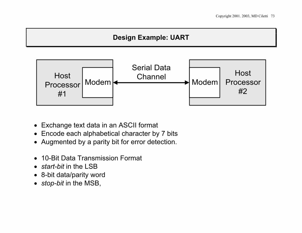
Design Example: UART
ModemHost
Processor#1
ModemHost
Processor#2
Serial DataChannel
• Exchange text data in an ASCII format • Encode each alphabetical character by 7 bits • Augmented by a parity bit for error detection.
• 10-Bit Data Transmission Format • start-bit in the LSB • 8-bit data/parity word • stop-bit in the MSB,
Copyright 2001. 2003, MD Ciletti 74
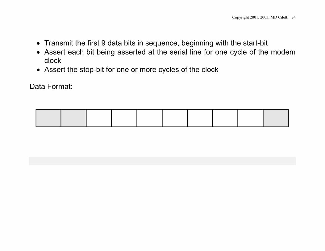
• Transmit the first 9 data bits in sequence, beginning with the start-bit • Assert each bit being asserted at the serial line for one cycle of the modem
clock • Assert the stop-bit for one or more cycles of the clock
Data Format:
Copyright 2001. 2003, MD Ciletti 75
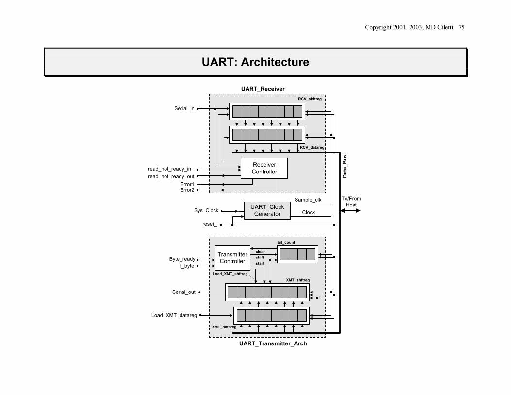
UART: Architecture
RCV_datareg
RCV_shftreg
XMT_datareg
XMT_shftreg
Serial_in
T_byte
Serial_out1
UART_Receiver
UART_Transmitter_Arch
Sys_Clock
TransmitterController
UART ClockGenerator
ReceiverController
Load_XMT_datareg
Dat
a_B
us
Byte_ready
To/FromHost
Load_XMT_shftreg
shiftclear
bit_count
start
Sample_clk
Clock
reset_
read_not_ready_inread_not_ready_out
Error1Error2
Copyright 2001. 2003, MD Ciletti 76
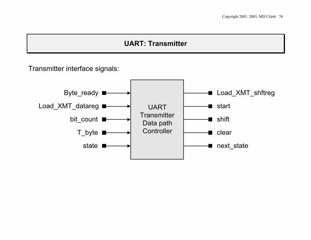
UART: Transmitter
Transmitter interface signals:
UARTTransmitterData pathController
Byte_ready
Load_XMT_datareg
bit_count
T_byte
state
Load_XMT_shftreg
start
shift
clear
next_state
Copyright 2001. 2003, MD Ciletti 77
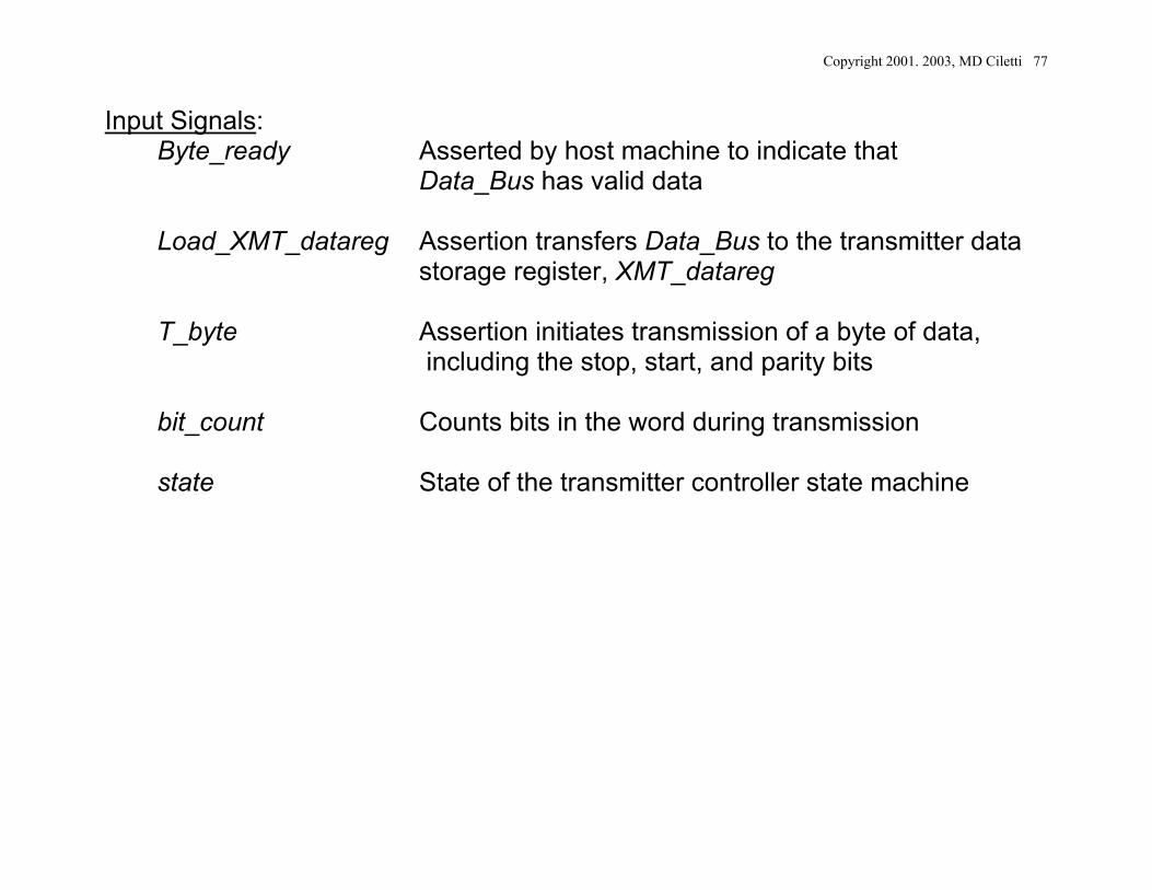
Input Signals: Byte_ready Asserted by host machine to indicate that
Data_Bus has valid data Load_XMT_datareg Assertion transfers Data_Bus to the transmitter data
storage register, XMT_datareg T_byte Assertion initiates transmission of a byte of data,
including the stop, start, and parity bits
bit_count Counts bits in the word during transmission
state State of the transmitter controller state machine
Copyright 2001. 2003, MD Ciletti 78
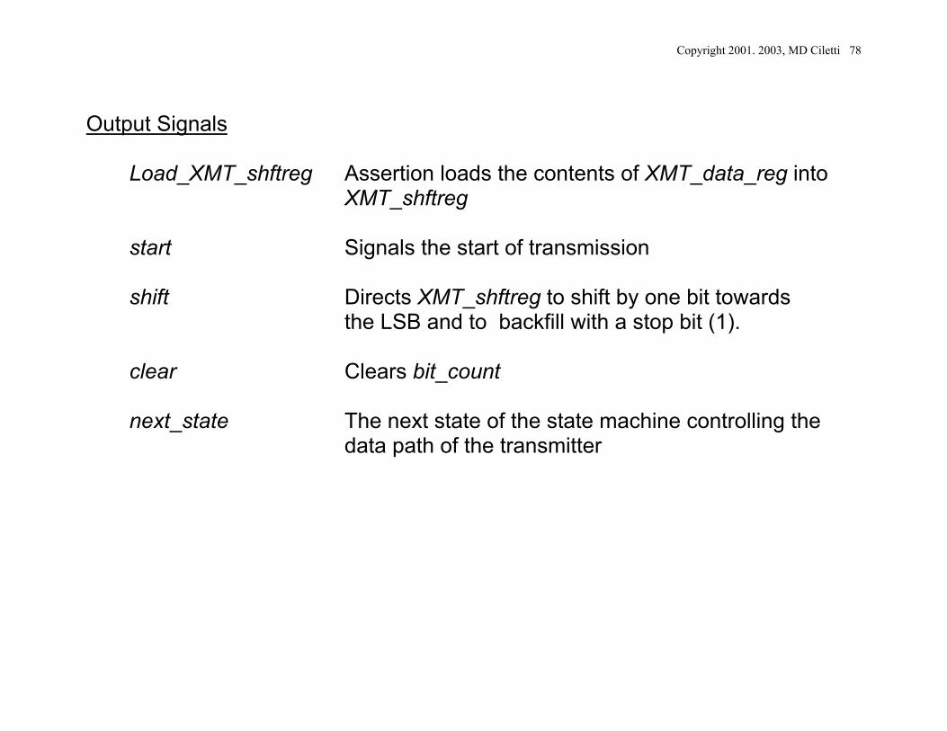
Output Signals
Load_XMT_shftreg Assertion loads the contents of XMT_data_reg into XMT_shftreg start Signals the start of transmission shift Directs XMT_shftreg to shift by one bit towards
the LSB and to backfill with a stop bit (1). clear Clears bit_count next_state The next state of the state machine controlling the data path of the transmitter
Copyright 2001. 2003, MD Ciletti 79
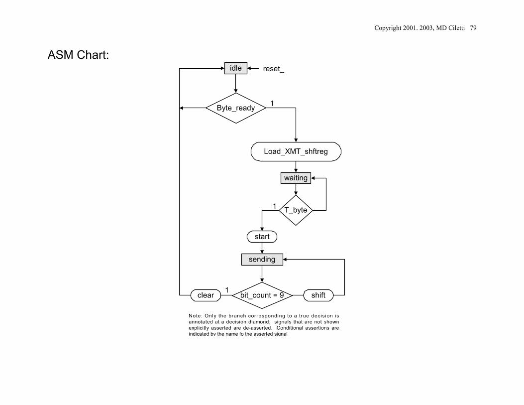
ASM Chart: idle
Load_XMT_shftreg
Byte_ready
waiting
start
sending
bit_count = 9
1
1
1
T_byte
Note: Only the branch corresponding to a true decision isannotated at a decision diamond; signals that are not shownexplicitly asserted are de-asserted. Conditional assertions areindicated by the name fo the asserted signal
reset_
shiftclear
Copyright 2001. 2003, MD Ciletti 80
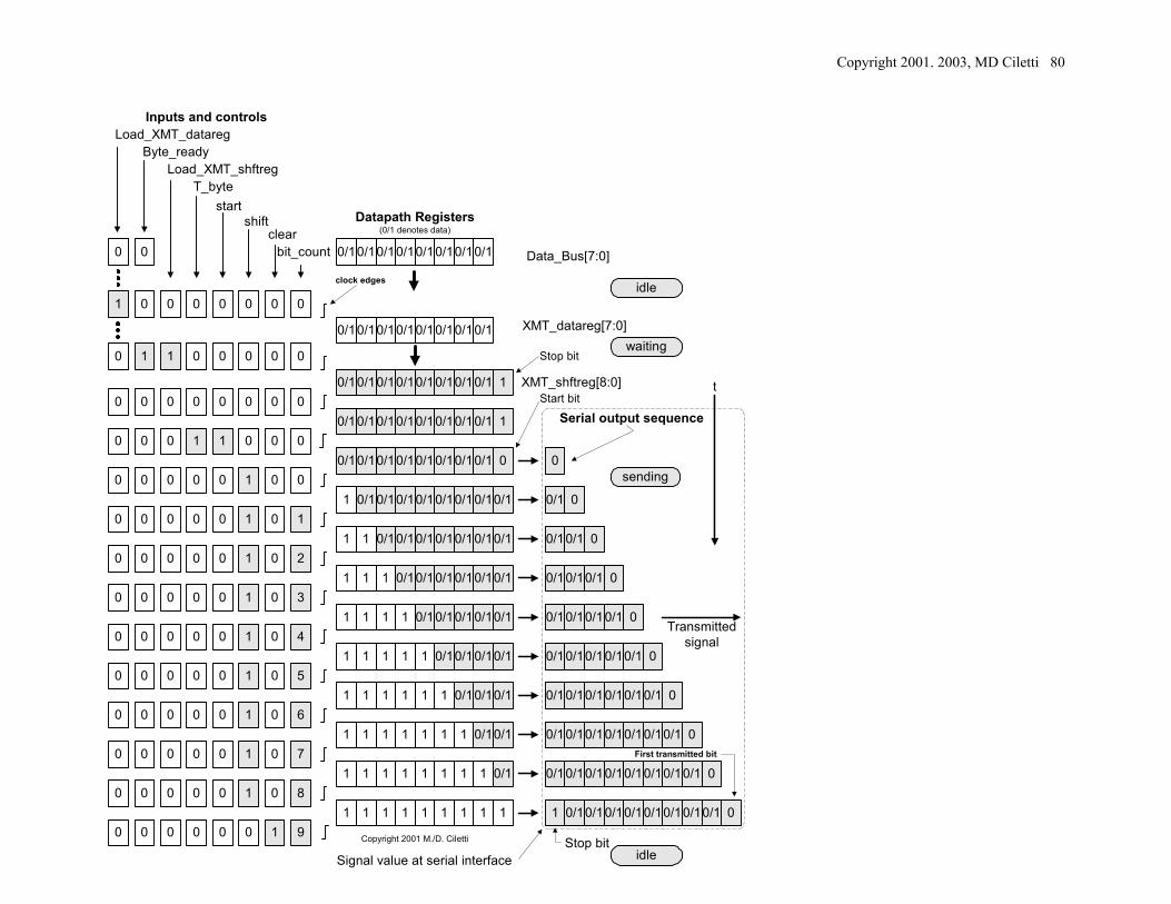
0/10/10/10/10/10/10/10/1
10/10/10/10/10/10/10/10/1
0/10/10/10/10/10/10/10/1
0/10/10/10/10/10/10/11
0/10/10/10/10/10/111
1
0/1
0/1
0/1 0
0/10/10/10/10/1111 0/1
0/10/1 0
1
1
0/11111 0/1 00/10/10/10/10/1 0/1
1 1 11111 0/1 00/10/10/10/10/1 0/10/1
1 1 1 11111 00/10/10/10/10/1 0/10/10/1
1 1 1 11111 1 00/10/10/10/11 0/10/10/10/1
Start bitXMT_shftreg[8:0]
XMT_datareg[7:0]
Stop bit
Stop bit
01 0 0
Load_XMT_datareg
startshift
bit_count
0 0
0/10/10/10/10/10/10/10/1 Data_Bus[7:0]
10 0 0 0 0
0 0 0 1 0 0
0 0 0 0 0
0 0 0 1 0 1
0 0 0 1 0 2
clear
t
0 0 0 1 0 8
0 0 0 1 0 7
0 0 0 1 0 6
0 0 0 1 0 5
T_byte
idle
sending
waiting
0/10/10/10/1111 0/1
0/10/1 00 0 0 1 0 3
1
0/10/10/1111 0/1 0/10 0 0 1 0 4
1
1 0/1
0/1
0/1
0/1
0/10/1 00/10/1
0/10/1 00/10/1
0 0 0 0 1 9 Copyright 2001 M./D. Ciletti
0
idle
Byte_ready
0
0
0
1
0
0
0
0
0
0
0
0
0
0
0
0
0
0
0
0
0
0
0
0
0
Load_XMT_shftreg
0/10/10/10/10/10/10/10/1 0 00 0 1 0 0 00
0
0
1
0
Inputs and controls
Datapath Registers
Serial output sequence
(0/1 denotes data)
Transmittedsignal
Signal value at serial interface
First transmitted bit
clock edges
Copyright 2001. 2003, MD Ciletti 81
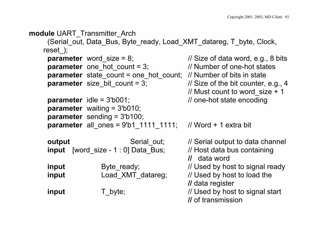
module UART_Transmitter_Arch (Serial_out, Data_Bus, Byte_ready, Load_XMT_datareg, T_byte, Clock, reset_); parameter word_size = 8; // Size of data word, e.g., 8 bits parameter one_hot_count = 3; // Number of one-hot states parameter state_count = one_hot_count; // Number of bits in state parameter size_bit_count = 3; // Size of the bit counter, e.g., 4
// Must count to word_size + 1 parameter idle = 3'b001; // one-hot state encoding parameter waiting = 3'b010; parameter sending = 3'b100; parameter all_ones = 9'b1_1111_1111; // Word + 1 extra bit output Serial_out; // Serial output to data channel input [word_size - 1 : 0] Data_Bus; // Host data bus containing
// data word input Byte_ready; // Used by host to signal ready input Load_XMT_datareg; // Used by host to load the
// data register input T_byte; // Used by host to signal start
// of transmission
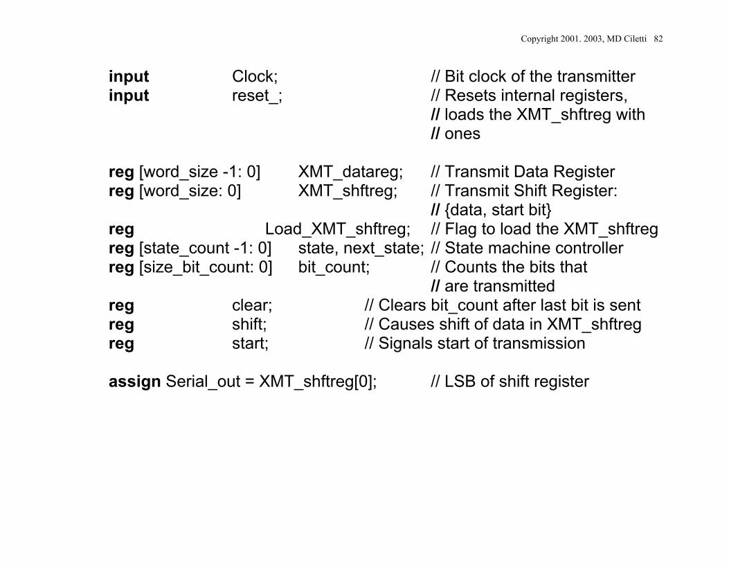
Copyright 2001. 2003, MD Ciletti 82
input Clock; // Bit clock of the transmitter input reset_; // Resets internal registers,
// loads the XMT_shftreg with // ones
reg [word_size -1: 0] XMT_datareg; // Transmit Data Register reg [word_size: 0] XMT_shftreg; // Transmit Shift Register:
// {data, start bit} reg Load_XMT_shftreg; // Flag to load the XMT_shftreg reg [state_count -1: 0] state, next_state; // State machine controller reg [size_bit_count: 0] bit_count; // Counts the bits that
// are transmitted reg clear; // Clears bit_count after last bit is sent reg shift; // Causes shift of data in XMT_shftreg reg start; // Signals start of transmission assign Serial_out = XMT_shftreg[0]; // LSB of shift register
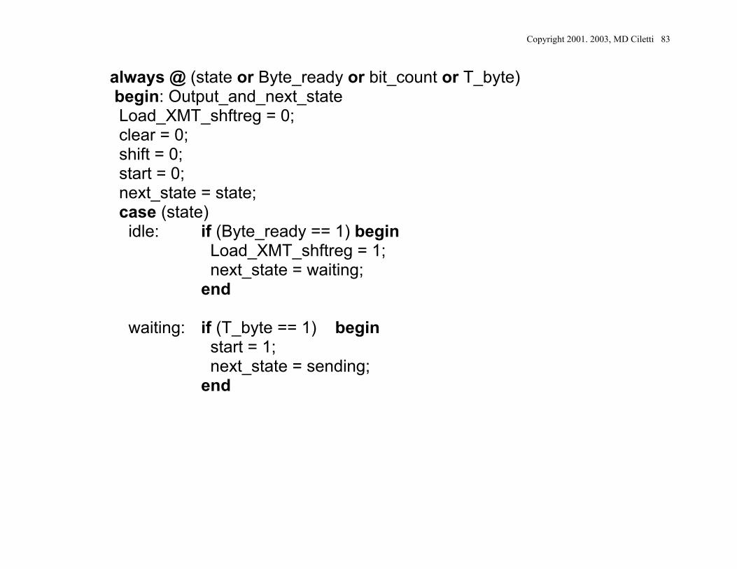
Copyright 2001. 2003, MD Ciletti 83
always @ (state or Byte_ready or bit_count or T_byte) begin: Output_and_next_state Load_XMT_shftreg = 0; clear = 0; shift = 0; start = 0; next_state = state; case (state) idle: if (Byte_ready == 1) begin Load_XMT_shftreg = 1; next_state = waiting; end waiting: if (T_byte == 1) begin start = 1; next_state = sending; end
Copyright 2001. 2003, MD Ciletti 84
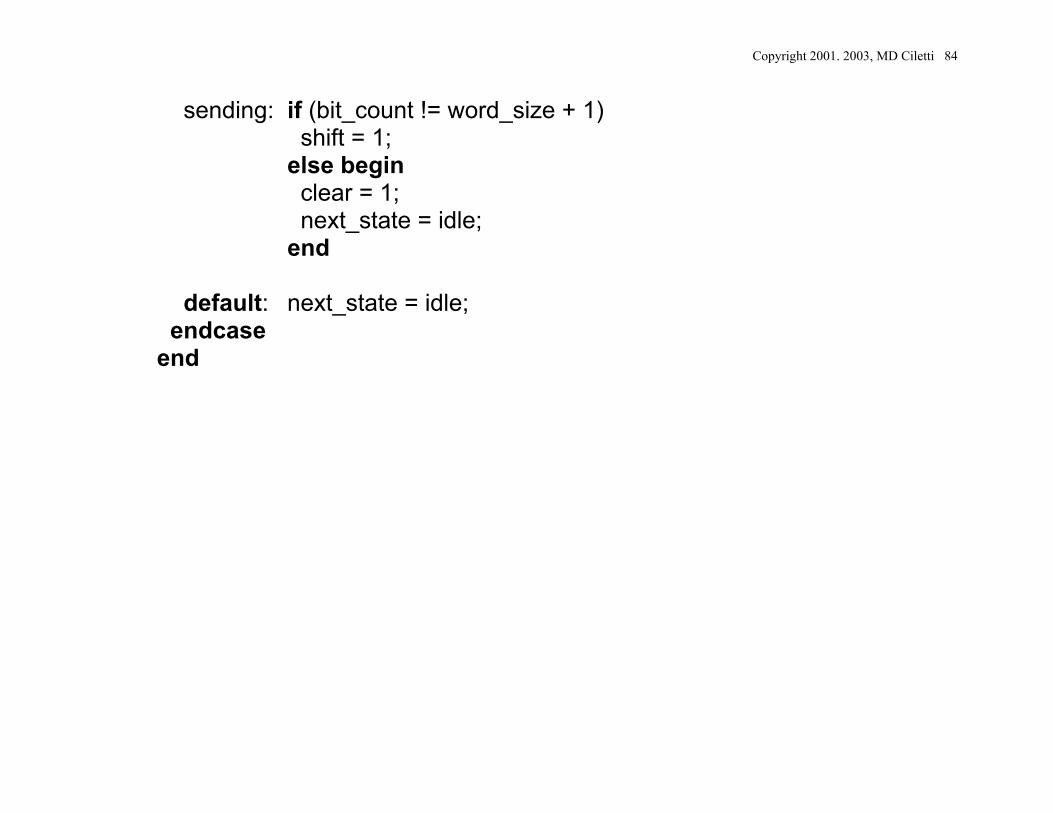
sending: if (bit_count != word_size + 1) shift = 1;
else begin clear = 1; next_state = idle; end default: next_state = idle; endcase end
Copyright 2001. 2003, MD Ciletti 85
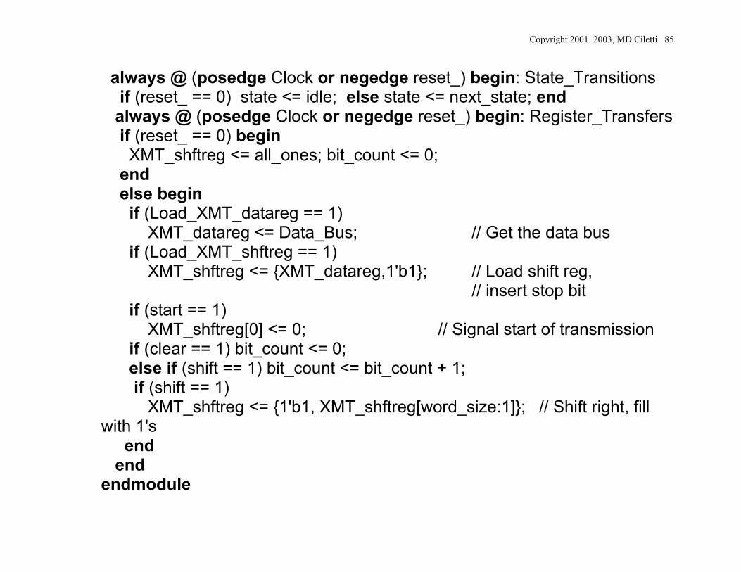
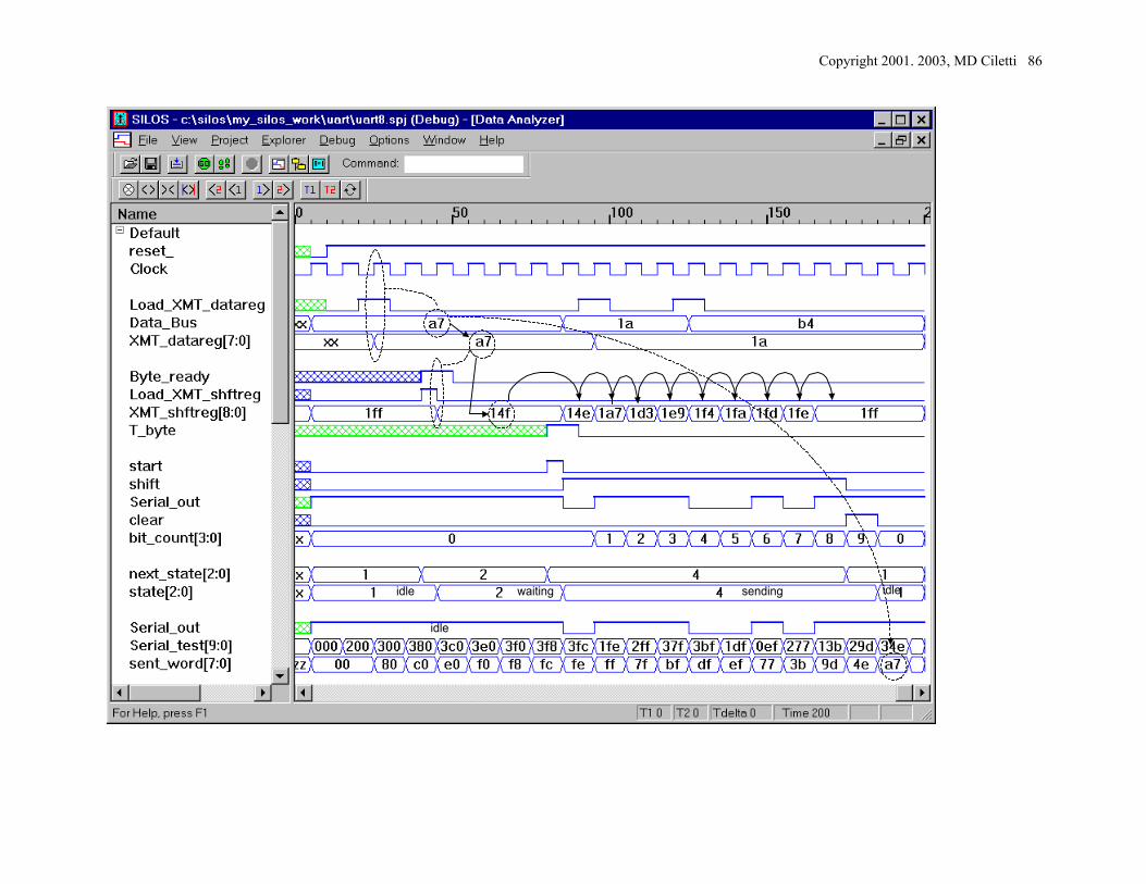
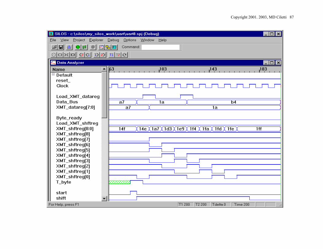
always @ (posedge Clock or negedge reset_) begin: State_Transitions if (reset_ == 0) state <= idle; else state <= next_state; end always @ (posedge Clock or negedge reset_) begin: Register_Transfers if (reset_ == 0) begin XMT_shftreg <= all_ones; bit_count <= 0; end else begin if (Load_XMT_datareg == 1) XMT_datareg <= Data_Bus; // Get the data bus if (Load_XMT_shftreg == 1) XMT_shftreg <= {XMT_datareg,1'b1}; // Load shift reg, // insert stop bit if (start == 1) XMT_shftreg[0] <= 0; // Signal start of transmission if (clear == 1) bit_count <= 0; else if (shift == 1) bit_count <= bit_count + 1; if (shift == 1) XMT_shftreg <= {1'b1, XMT_shftreg[word_size:1]}; // Shift right, fill with 1's end end endmodule
Copyright 2001. 2003, MD Ciletti 86
idle idle
idle
waiting sending
Copyright 2001. 2003, MD Ciletti 87
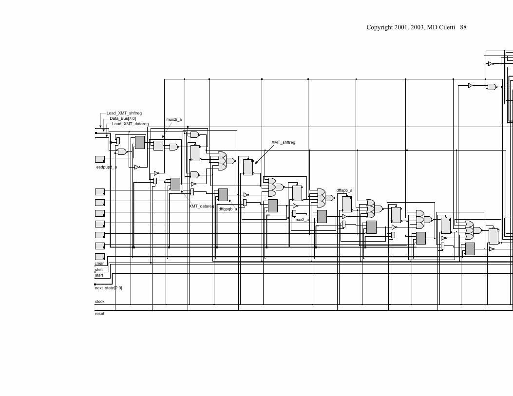
Copyright 2001. 2003, MD Ciletti 88
reset
clock
next_state[2:0]
clearshiftstart
Load_XMT_shftregData_Bus[7:0]
Load_XMT_datareg
dffspb_a
dffgpqb_a
mux2_a
mux2i_a
esdpupd_a
XMT_shftreg
XMT_datareg
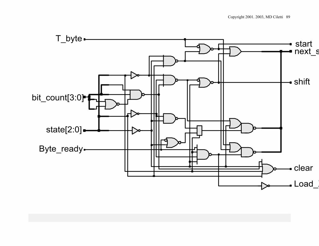
Copyright 2001. 2003, MD Ciletti 89
T_byte
bit_count[3:0]
state[2:0]
Byte_ready
shift
next_s
clear
Load_X
start
Copyright 2001. 2003, MD Ciletti 90
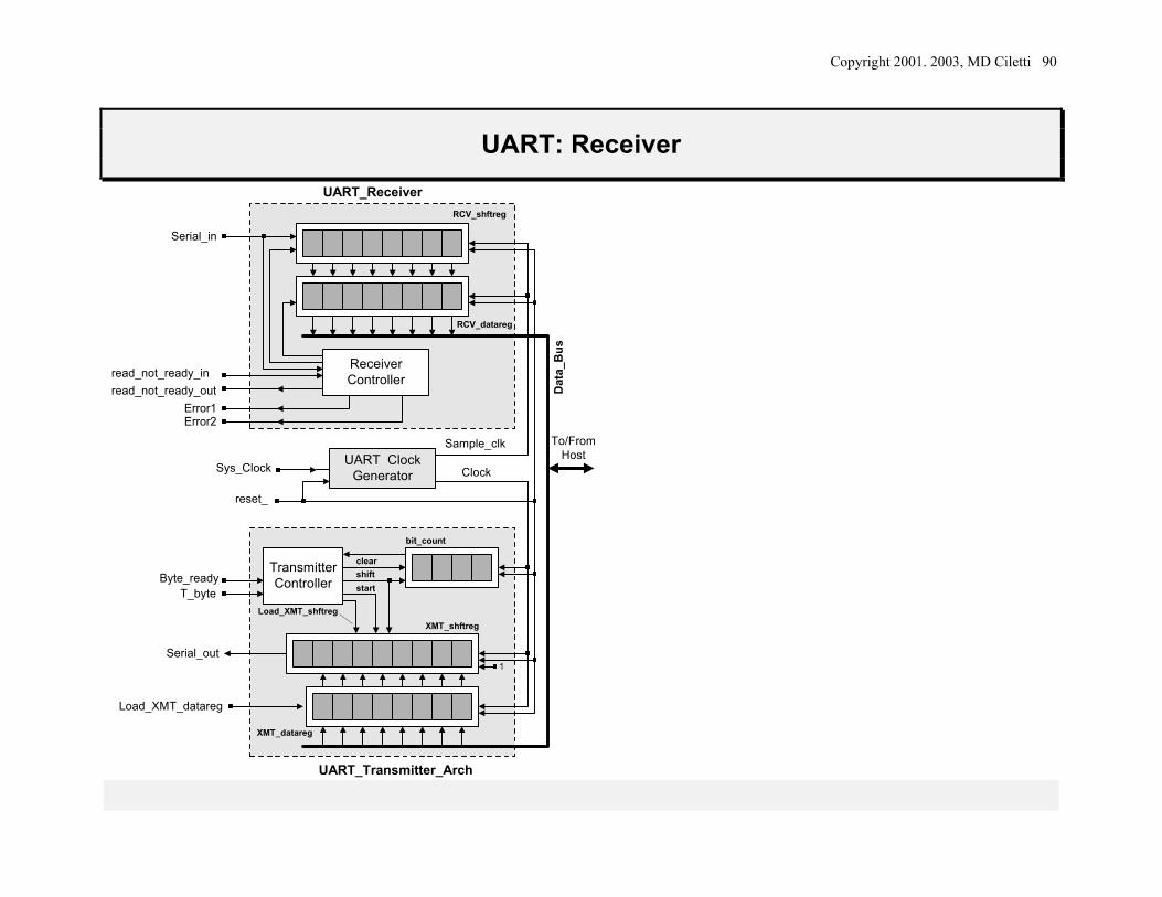
UART: Receiver
RCV_datareg
RCV_shftreg
XMT_datareg
XMT_shftreg
Serial_in
T_byte
Serial_out1
UART_Receiver
UART_Transmitter_Arch
Sys_Clock
TransmitterController
UART ClockGenerator
ReceiverController
Load_XMT_datareg
Dat
a_B
usByte_ready
To/FromHost
Load_XMT_shftreg
shiftclear
bit_count
start
Sample_clk
Clock
reset_
read_not_ready_inread_not_ready_out
Error1Error2
Copyright 2001. 2003, MD Ciletti 91
UART: Receiver (cont.)
Receiver action: • Receives the serial bit-stream of data • Removes the start-bit • Transfer data in a parallel format to a storage register connected to the host
data bus. Clock Regeneration: • Data arrives at a standard bit rate • Data is not necessarily synchronized with the internal clock at the host of the
receiver • Transmitter’s clock is not available to the receiver • Generate a local clock at a higher frequency, and using it to sample the
received data in a manner that preserves the integrity of the data. • Sample_clock is generated at the receiver’s host. • Count the cycles of Sample_clock to ensure that the data is sampled in the
middle of a bit time,
Copyright 2001. 2003, MD Ciletti 92
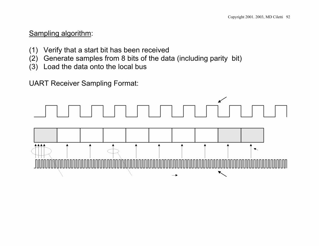
Sampling algorithm: (1) Verify that a start bit has been received (2) Generate samples from 8 bits of the data (including parity bit) (3) Load the data onto the local bus UART Receiver Sampling Format:
Copyright 2001. 2003, MD Ciletti 93
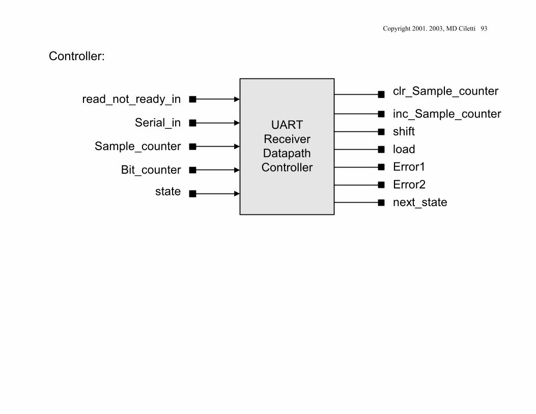
Controller:
UARTReceiverDatapathController
read_not_ready_in
Serial_in
Sample_counter
Bit_counter
clr_Sample_counter
inc_Sample_countershiftloadError1Error2next_state
state
Copyright 2001. 2003, MD Ciletti 94
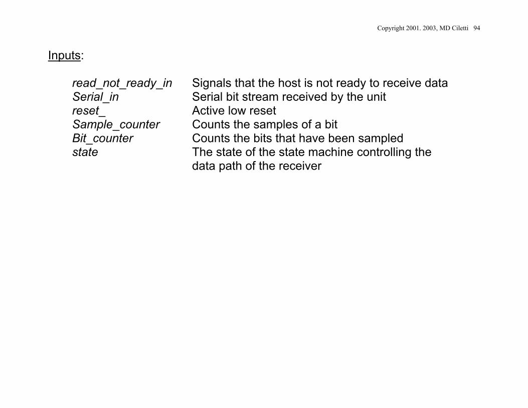
Inputs:
read_not_ready_in Signals that the host is not ready to receive data Serial_in Serial bit stream received by the unit reset_ Active low reset Sample_counter Counts the samples of a bit Bit_counter Counts the bits that have been sampled state The state of the state machine controlling the
data path of the receiver
Copyright 2001. 2003, MD Ciletti 95
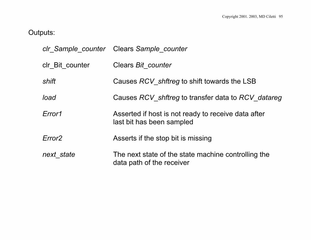
Outputs:
clr_Sample_counter Clears Sample_counter clr_Bit_counter Clears Bit_counter shift Causes RCV_shftreg to shift towards the LSB load Causes RCV_shftreg to transfer data to RCV_datareg Error1 Asserted if host is not ready to receive data after
last bit has been sampled
Error2 Asserts if the stop bit is missing next_state The next state of the state machine controlling the data path of the receiver
Copyright 2001. 2003, MD Ciletti 96
ASM chart: id
le
clr_
Sam
ple_
coun
ter
Ser
ial_
in =
0
star
ting
rece
ivin
g
Erro
r1
1
Ser
ial_
in =
111
Sam
ple_
coun
ter
= 3
shift
inc_
Bit_
coun
ter
1
1
read
_not
_rea
dy_o
utcl
r_B
it_co
unte
r
read
_not
_rea
dy_i
n1
Erro
r2
1lo
ad
rese
t_
inc_
Sam
ple_
coun
ter
inc_
Sam
ple_
coun
ter
clr_
Sam
ple_
coun
ter
Sam
ple_
coun
ter
< 7
clr_
Sam
ple_
coun
ter
Bit_
coun
ter
= 8
Ser
ial_
in =
0
Copyright 2001. 2003, MD Ciletti 97
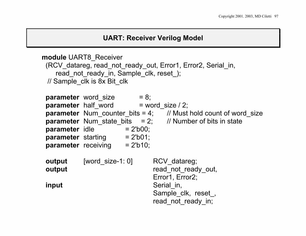
UART: Receiver Verilog Model
module UART8_Receiver (RCV_datareg, read_not_ready_out, Error1, Error2, Serial_in,
read_not_ready_in, Sample_clk, reset_); // Sample_clk is 8x Bit_clk parameter word_size = 8; parameter half_word = word_size / 2; parameter Num_counter_bits = 4; // Must hold count of word_size parameter Num_state_bits = 2; // Number of bits in state parameter idle = 2'b00; parameter starting = 2'b01; parameter receiving = 2'b10; output [word_size-1: 0] RCV_datareg; output read_not_ready_out, Error1, Error2; input Serial_in, Sample_clk, reset_, read_not_ready_in;
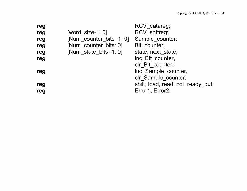
Copyright 2001. 2003, MD Ciletti 98
reg RCV_datareg; reg [word_size-1: 0] RCV_shftreg; reg [Num_counter_bits -1: 0] Sample_counter; reg [Num_counter_bits: 0] Bit_counter; reg [Num_state_bits -1: 0] state, next_state; reg inc_Bit_counter,
clr_Bit_counter; reg inc_Sample_counter,
clr_Sample_counter; reg shift, load, read_not_ready_out;
reg Error1, Error2;
Copyright 2001. 2003, MD Ciletti 99
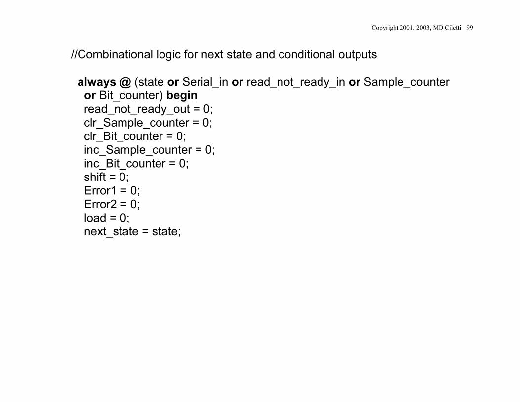
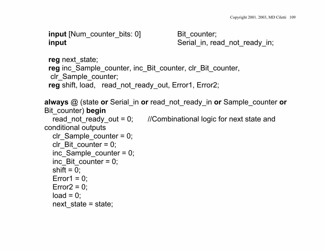
//Combinational logic for next state and conditional outputs always @ (state or Serial_in or read_not_ready_in or Sample_counter or Bit_counter) begin read_not_ready_out = 0; clr_Sample_counter = 0; clr_Bit_counter = 0; inc_Sample_counter = 0; inc_Bit_counter = 0; shift = 0; Error1 = 0; Error2 = 0; load = 0; next_state = state;
Copyright 2001. 2003, MD Ciletti 100
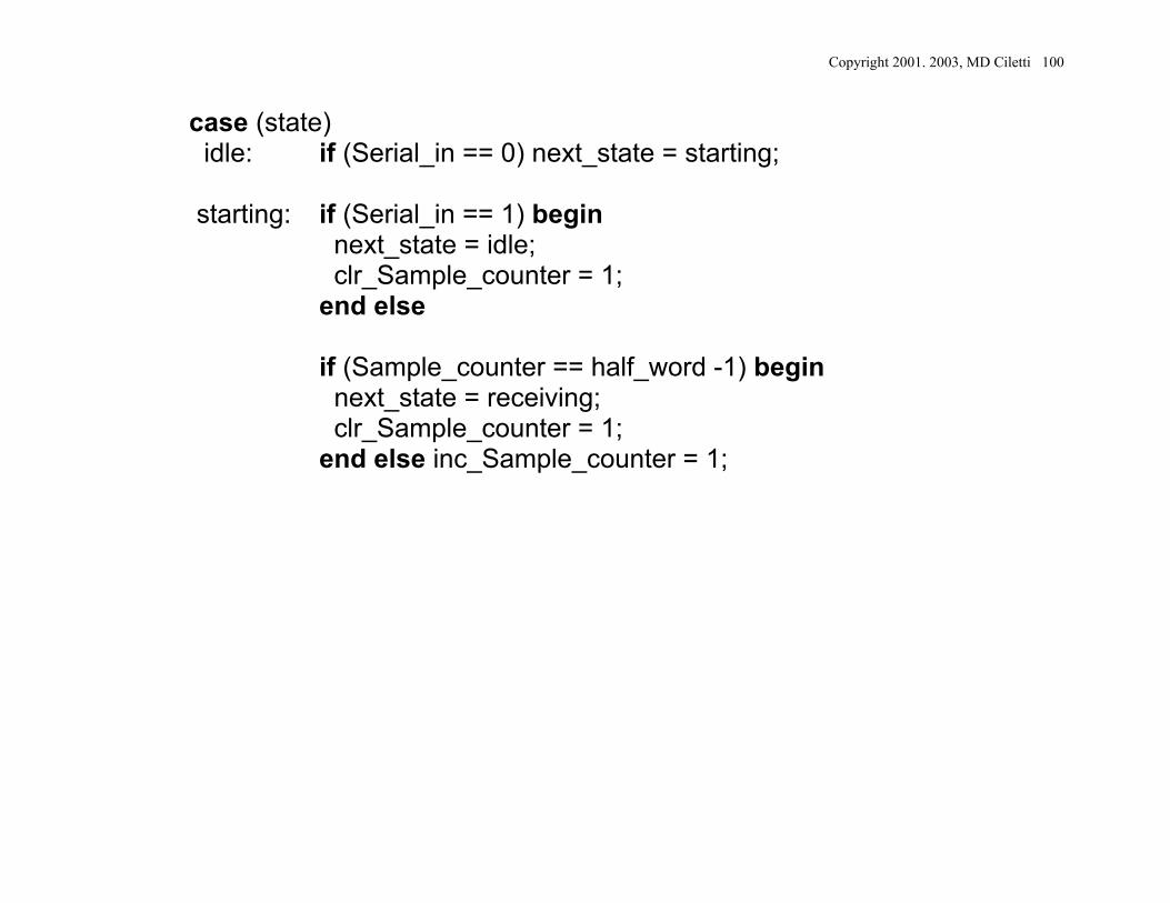
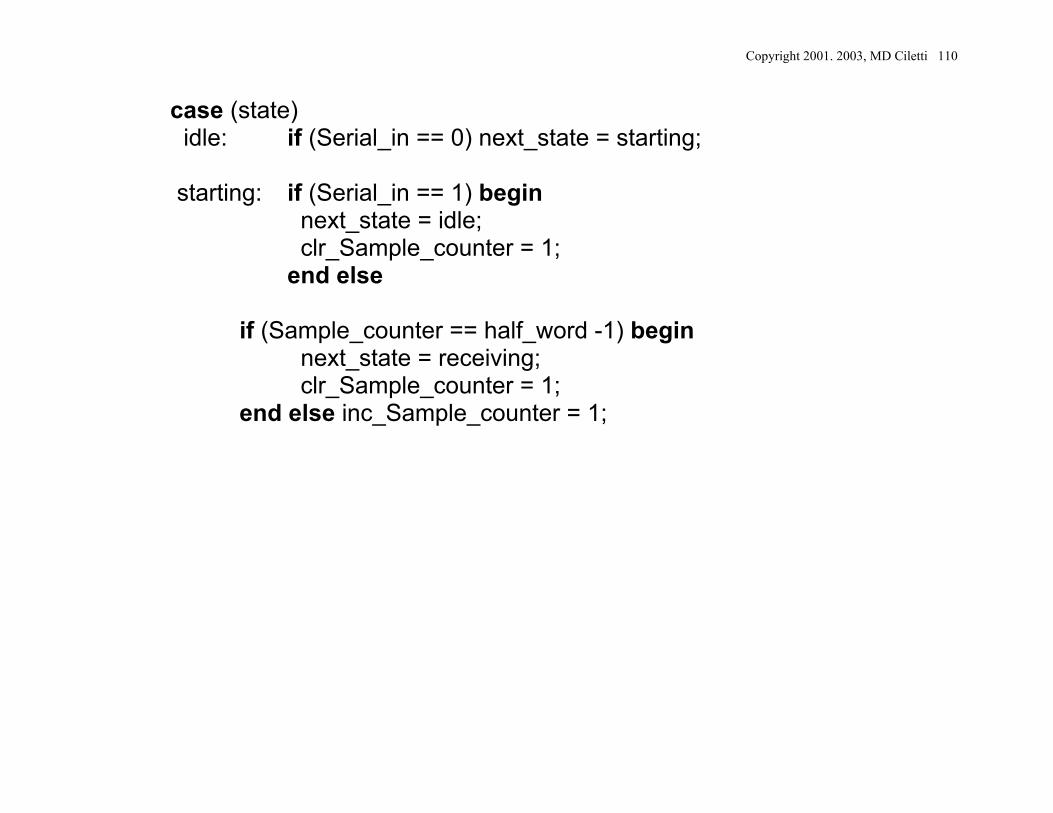
case (state) idle: if (Serial_in == 0) next_state = starting; starting: if (Serial_in == 1) begin next_state = idle; clr_Sample_counter = 1; end else if (Sample_counter == half_word -1) begin next_state = receiving; clr_Sample_counter = 1; end else inc_Sample_counter = 1;
Copyright 2001. 2003, MD Ciletti 101
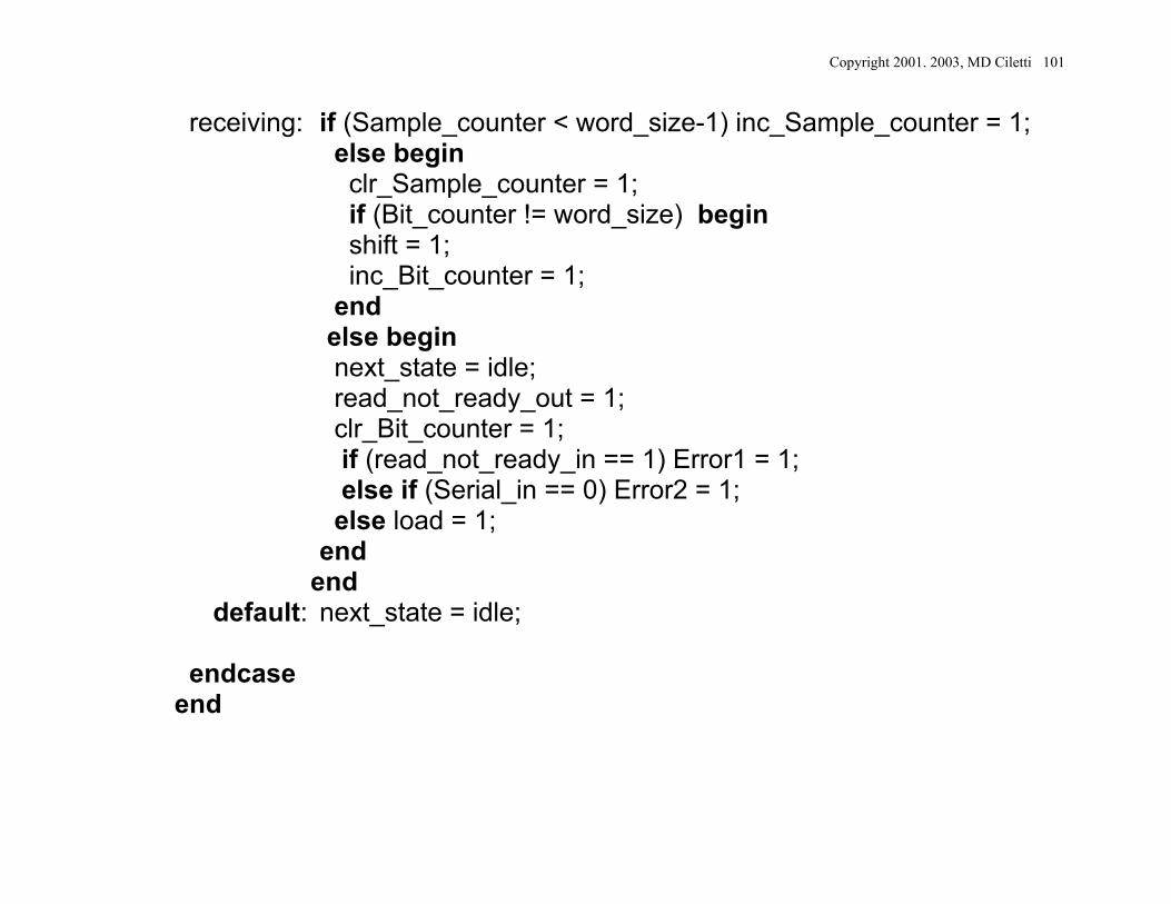
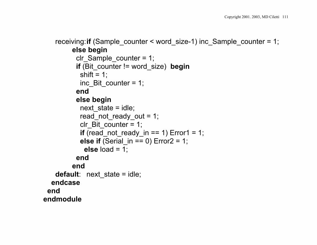
receiving: if (Sample_counter < word_size-1) inc_Sample_counter = 1; else begin clr_Sample_counter = 1; if (Bit_counter != word_size) begin shift = 1; inc_Bit_counter = 1; end else begin next_state = idle; read_not_ready_out = 1; clr_Bit_counter = 1; if (read_not_ready_in == 1) Error1 = 1; else if (Serial_in == 0) Error2 = 1; else load = 1; end end default: next_state = idle; endcase end
Copyright 2001. 2003, MD Ciletti 102
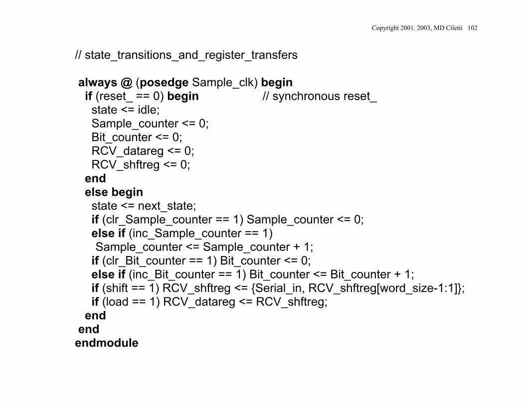
// state_transitions_and_register_transfers always @ (posedge Sample_clk) begin if (reset_ == 0) begin // synchronous reset_ state <= idle; Sample_counter <= 0; Bit_counter <= 0; RCV_datareg <= 0; RCV_shftreg <= 0; end else begin state <= next_state; if (clr_Sample_counter == 1) Sample_counter <= 0; else if (inc_Sample_counter == 1)
Sample_counter <= Sample_counter + 1; if (clr_Bit_counter == 1) Bit_counter <= 0; else if (inc_Bit_counter == 1) Bit_counter <= Bit_counter + 1; if (shift == 1) RCV_shftreg <= {Serial_in, RCV_shftreg[word_size-1:1]}; if (load == 1) RCV_datareg <= RCV_shftreg; end end endmodule
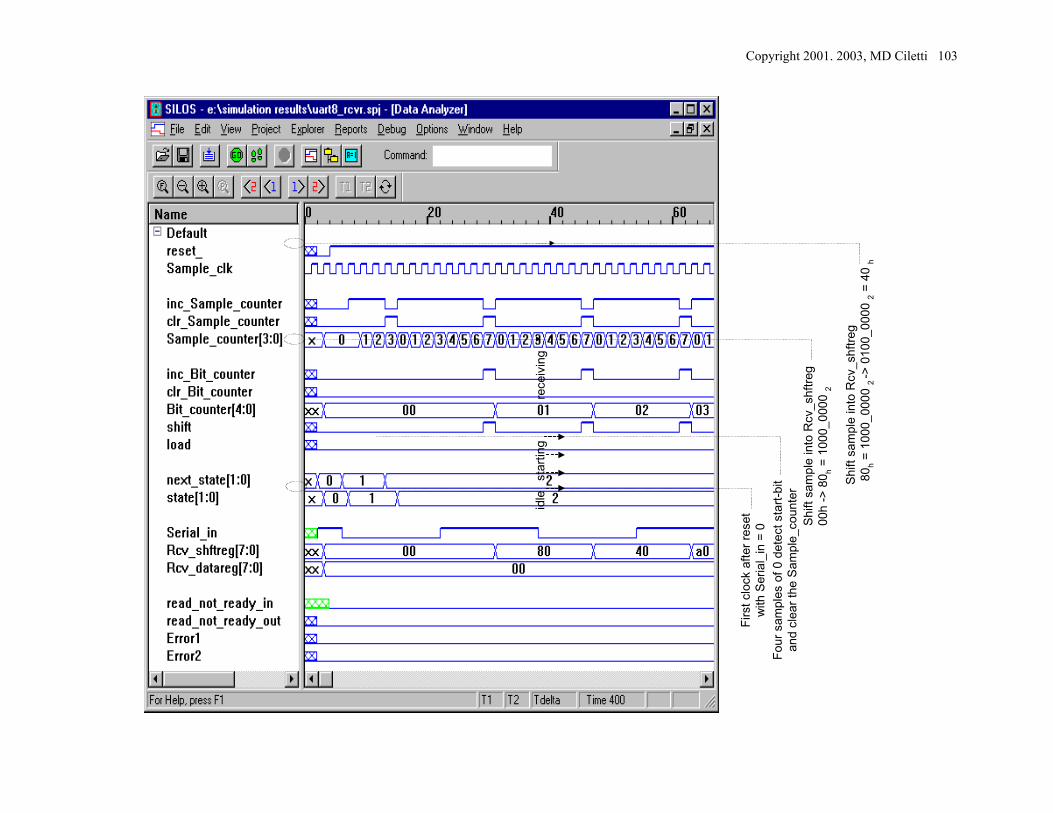
Copyright 2001. 2003, MD Ciletti 103
Firs
t clo
ck a
fter r
eset
with
Ser
ial_
in =
0
star
ting
rece
ivin
g
Four
sam
ples
of 0
det
ect s
tart-
bit
and
clea
r the
Sam
ple_
coun
ter
Shi
ft sa
mpl
e in
to R
cv_s
hftre
g00
h ->
80 h =
100
0_00
00 2
Shi
ft sa
mpl
e in
to R
cv_s
hftre
g 8
0 h = 1
000_
0000
2 -> 0
100_
0000
2 = 4
0 h
idle
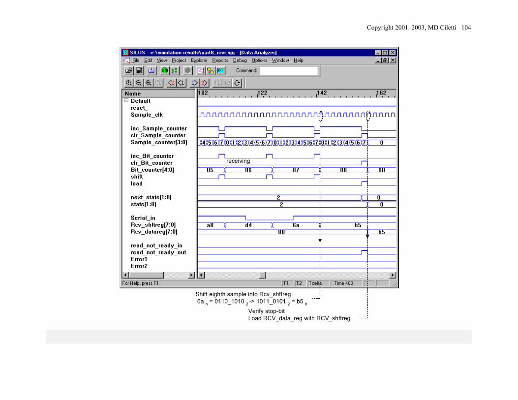
Copyright 2001. 2003, MD Ciletti 104
receiving
Verify stop-bitLoad RCV_data_reg with RCV_shftreg
Shift eighth sample into Rcv_shftreg 6a h = 0110_1010 2 -> 1011_0101 2 = b5 h
Copyright 2001. 2003, MD Ciletti 105
UART Receiver: Partitioned Model
module UART8_rcvr_partition (RCV_datareg, read_not_ready_out, Error1, Error2, Serial_in, read_not_ready_in, Sample_clk, reset_); // partitioned UART receiver // Sample_clk is 8x Bit_clk parameter word_size = 8; parameter half_word = word_size / 2; parameter Num_counter_bits = 4; // Must hold count of word_size parameter Num_state_bits = 2; // Number of bits in state parameter idle = 2'b00; parameter starting = 2'b01; parameter receiving = 2'b10;
Copyright 2001. 2003, MD Ciletti 106
output [word_size -1: 0] RCV_datareg; output read_not_ready_out,
// Handshake to host processor Error1, // Host not ready error Error2; // Data_in missing stop bit input Serial_in, // Serial data input Sample_clk, // Clock to sample serial data reset_, // Active-low reset read_not_ready_in; // Status bit from host processor wire [Num_counter_bits -1: 0] Sample_counter; wire [Num_counter_bits: 0] Bit_counter; wire [Num_state_bits -1: 0] state, next_state;
Copyright 2001. 2003, MD Ciletti 107
controller_part M2 (next_state, shift, load, read_not_ready_out, Error1, Error2, inc_Sample_counter, inc_Bit_counter, clr_Bit_counter, clr_Sample_counter, state, Sample_counter, Bit_counter, Serial_in, read_not_ready_in); state_transition_part M1 (RCV_datareg, Sample_counter, Bit_counter, state, next_state, clr_Sample_counter, inc_Sample_counter, clr_Bit_counter, inc_Bit_counter, shift, load, Serial_in, Sample_clk, reset_); endmodule
Copyright 2001. 2003, MD Ciletti 108
module controller_part (next_state, shift, load, read_not_ready_out, Error1, Error2, inc_Sample_counter, inc_Bit_counter, clr_Bit_counter, clr_Sample_counter, state, Sample_counter, Bit_counter, Serial_in, read_not_ready_in); parameter word_size = 8; parameter half_word = word_size / 2; parameter Num_counter_bits = 4; // Must hold count of word_size parameter Num_state_bits = 2; // Number of bits in state parameter idle = 2'b00; parameter starting = 2'b01; parameter receiving = 2'b10; output [Num_state_bits -1: 0] next_state; output shift, load, inc_Sample_counter; output inc_Bit_counter, clr_Bit_counter,
clr_Sample_counter; output read_not_ready_out, Error1, Error2; input [Num_state_bits -1: 0] state; input [Num_counter_bits -1: 0] Sample_counter;
Copyright 2001. 2003, MD Ciletti 109
input [Num_counter_bits: 0] Bit_counter; input Serial_in, read_not_ready_in; reg next_state; reg inc_Sample_counter, inc_Bit_counter, clr_Bit_counter, clr_Sample_counter; reg shift, load, read_not_ready_out, Error1, Error2; always @ (state or Serial_in or read_not_ready_in or Sample_counter or Bit_counter) begin read_not_ready_out = 0; //Combinational logic for next state and conditional outputs clr_Sample_counter = 0; clr_Bit_counter = 0; inc_Sample_counter = 0; inc_Bit_counter = 0; shift = 0; Error1 = 0; Error2 = 0; load = 0; next_state = state;
Copyright 2001. 2003, MD Ciletti 110
case (state) idle: if (Serial_in == 0) next_state = starting; starting: if (Serial_in == 1) begin next_state = idle; clr_Sample_counter = 1; end else if (Sample_counter == half_word -1) begin next_state = receiving; clr_Sample_counter = 1; end else inc_Sample_counter = 1;
Copyright 2001. 2003, MD Ciletti 111
receiving: if (Sample_counter < word_size-1) inc_Sample_counter = 1; else begin clr_Sample_counter = 1; if (Bit_counter != word_size) begin shift = 1; inc_Bit_counter = 1; end else begin next_state = idle; read_not_ready_out = 1; clr_Bit_counter = 1; if (read_not_ready_in == 1) Error1 = 1; else if (Serial_in == 0) Error2 = 1; else load = 1; end end default: next_state = idle; endcase end endmodule
Copyright 2001. 2003, MD Ciletti 112
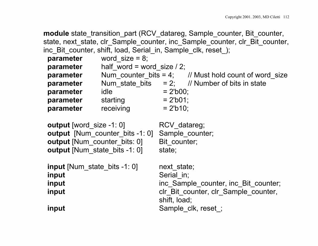
module state_transition_part (RCV_datareg, Sample_counter, Bit_counter, state, next_state, clr_Sample_counter, inc_Sample_counter, clr_Bit_counter, inc_Bit_counter, shift, load, Serial_in, Sample_clk, reset_); parameter word_size = 8; parameter half_word = word_size / 2; parameter Num_counter_bits = 4; // Must hold count of word_size parameter Num_state_bits = 2; // Number of bits in state parameter idle = 2'b00; parameter starting = 2'b01; parameter receiving = 2'b10; output [word_size -1: 0] RCV_datareg; output [Num_counter_bits -1: 0] Sample_counter; output [Num_counter_bits: 0] Bit_counter; output [Num_state_bits -1: 0] state; input [Num_state_bits -1: 0] next_state; input Serial_in; input inc_Sample_counter, inc_Bit_counter; input clr_Bit_counter, clr_Sample_counter,
shift, load; input Sample_clk, reset_;
Copyright 2001. 2003, MD Ciletti 113
reg Sample_counter, Bit_counter; reg [word_size-1: 0] RCV_shftreg, RCV_datareg; reg state; // state_transitions_and_datapath_register_transfers always @ (posedge Sample_clk) begin if (reset_ == 0) begin // synchronous reset_ state <= idle; Sample_counter <= 0; Bit_counter <= 0; RCV_datareg <= 0; RCV_shftreg <= 0; end else begin state <= next_state; if (clr_Sample_counter == 1) Sample_counter <= 0; else if (inc_Sample_counter == 1) Sample_counter <= Sample_counter + 1;
Copyright 2001. 2003, MD Ciletti 114
if (clr_Bit_counter == 1) Bit_counter <= 0; else if (inc_Bit_counter == 1) Bit_counter <= Bit_counter + 1; if (shift == 1) RCV_shftreg <= {Serial_in, RCV_shftreg[word_size-1: 1]}; if (load == 1) RCV_datareg <= RCV_shftreg; end end endmodule
Copyright 2001. 2003, MD Ciletti 115
Sample_counter[3:0]
shiftError1Error2load
inc_Bit_co
clr_Sampl
next_state
clr_Bit_cou
inc_Samplread_not_
Serial_in
read_not_ready_in
state[1:0]Bit_counter[4:0]
Copyright 2001. 2003, MD Ciletti 116
dffrgpqb_a
Bit_counter[4:0]
state[1:0]
Sample_counter[3:0]
RCV_datareg[7:0]
+1
next_state[1:0]
inc_Bit_counter
clr_Sample_counterinc_Sample_counter
clr_Bit_counter
resetshift
Serial_inSample_clk
load
RCV_shftreg[7:0]
[7]
[0]
mux2_a
[4]
[0]
[3]
[2]
[1]
[0]dffrpqb_a
dffrgpqb_a
Copyright 2001. 2003, MD Ciletti 117