Embed Size (px)
Citation preview
R
Advanced ChipSync Applications
XAPP707 (v1.0) October 31, 2006

Advanced ChipSync Applications www.xilinx.com XAPP707 (v1.0) October 31, 2006
Xilinx is disclosing this Document and Intellectual Property (hereinafter “the Design”) to you for use in the development of designs to operate on, or interface with Xilinx FPGAs. Except as stated herein, none of the Design may be copied, reproduced, distributed, republished, downloaded, displayed, posted, or transmitted in any form or by any means including, but not limited to, electronic, mechanical, photocopying, recording, or otherwise, without the prior written consent of Xilinx. Any unauthorized use of the Design may violate copyright laws, trademark laws, the laws of privacy and publicity, and communications regulations and statutes.
Xilinx does not assume any liability arising out of the application or use of the Design; nor does Xilinx convey any license under its patents, copyrights, or any rights of others. You are responsible for obtaining any rights you may require for your use or implementation of the Design. Xilinx reserves the right to make changes, at any time, to the Design as deemed desirable in the sole discretion of Xilinx. Xilinx assumes no obligation to correct any errors contained herein or to advise you of any correction if such be made. Xilinx will not assume any liability for the accuracy or correctness of any engineering or technical support or assistance provided to you in connection with the Design.
THE DESIGN IS PROVIDED “AS IS” WITH ALL FAULTS, AND THE ENTIRE RISK AS TO ITS FUNCTION AND IMPLEMENTATION IS WITH YOU. YOU ACKNOWLEDGE AND AGREE THAT YOU HAVE NOT RELIED ON ANY ORAL OR WRITTEN INFORMATION OR ADVICE, WHETHER GIVEN BY XILINX, OR ITS AGENTS OR EMPLOYEES. XILINX MAKES NO OTHER WARRANTIES, WHETHER EXPRESS, IMPLIED, OR STATUTORY, REGARDING THE DESIGN, INCLUDING ANY WARRANTIES OF MERCHANTABILITY, FITNESS FOR A PARTICULAR PURPOSE, TITLE, AND NONINFRINGEMENT OF THIRD-PARTY RIGHTS.
IN NO EVENT WILL XILINX BE LIABLE FOR ANY CONSEQUENTIAL, INDIRECT, EXEMPLARY, SPECIAL, OR INCIDENTAL DAMAGES, INCLUDING ANY LOST DATA AND LOST PROFITS, ARISING FROM OR RELATING TO YOUR USE OF THE DESIGN, EVEN IF YOU HAVE BEEN ADVISED OF THE POSSIBILITY OF SUCH DAMAGES. THE TOTAL CUMULATIVE LIABILITY OF XILINX IN CONNECTION WITH YOUR USE OF THE DESIGN, WHETHER IN CONTRACT OR TORT OR OTHERWISE, WILL IN NO EVENT EXCEED THE AMOUNT OF FEES PAID BY YOU TO XILINX HEREUNDER FOR USE OF THE DESIGN. YOU ACKNOWLEDGE THAT THE FEES, IF ANY, REFLECT THE ALLOCATION OF RISK SET FORTH IN THIS AGREEMENT AND THAT XILINX WOULD NOT MAKE AVAILABLE THE DESIGN TO YOU WITHOUT THESE LIMITATIONS OF LIABILITY.
The Design is not designed or intended for use in the development of on-line control equipment in hazardous environments requiring fail-safe controls, such as in the operation of nuclear facilities, aircraft navigation or communications systems, air traffic control, life support, or weapons systems (“High-Risk Applications”). Xilinx specifically disclaims any express or implied warranties of fitness for such High-Risk Applications. You represent that use of the Design in such High-Risk Applications is fully at your risk.
© 2006 Xilinx, Inc. All rights reserved. XILINX, the Xilinx logo, and other designated brands included herein are trademarks of Xilinx, Inc. PowerPC is a trademark of IBM, Inc. All other trademarks are the property of their respective owners.
Revision HistoryThe following table shows the revision history for this document.
R
Date Version Revision
10/31/06 1.0 Initial Xilinx release.

Advanced ChipSync Applications www.xilinx.com 3XAPP707 (v1.0) October 31, 2006
Preface: About This GuideGuide Contents . . . . . . . . . . . . . . . . . . . . . . . . . . . . . . . . . . . . . . . . . . . . . . . . . . . . . . . . . . . . . . 5Additional Resources . . . . . . . . . . . . . . . . . . . . . . . . . . . . . . . . . . . . . . . . . . . . . . . . . . . . . . . . 5Conventions . . . . . . . . . . . . . . . . . . . . . . . . . . . . . . . . . . . . . . . . . . . . . . . . . . . . . . . . . . . . . . . . . 6
Typographical . . . . . . . . . . . . . . . . . . . . . . . . . . . . . . . . . . . . . . . . . . . . . . . . . . . . . . . . . . . . . 6Online Document . . . . . . . . . . . . . . . . . . . . . . . . . . . . . . . . . . . . . . . . . . . . . . . . . . . . . . . . . . 7
Chapter 1: IntroductionChipSync Overview . . . . . . . . . . . . . . . . . . . . . . . . . . . . . . . . . . . . . . . . . . . . . . . . . . . . . . . . . . 9ChipSync Applications . . . . . . . . . . . . . . . . . . . . . . . . . . . . . . . . . . . . . . . . . . . . . . . . . . . . . . . 9Characterization Resources . . . . . . . . . . . . . . . . . . . . . . . . . . . . . . . . . . . . . . . . . . . . . . . . . . 10
Chapter 2: IDELAY Block OperationDegradation in the IDELAY Tap Chain . . . . . . . . . . . . . . . . . . . . . . . . . . . . . . . . . . . . . . 12
Degradation Test Setup . . . . . . . . . . . . . . . . . . . . . . . . . . . . . . . . . . . . . . . . . . . . . . . . . . . . 12Degradation Test Results . . . . . . . . . . . . . . . . . . . . . . . . . . . . . . . . . . . . . . . . . . . . . . . . . . 15Degradation Analysis . . . . . . . . . . . . . . . . . . . . . . . . . . . . . . . . . . . . . . . . . . . . . . . . . . . . . 19Degradation Conclusion and Recommendations . . . . . . . . . . . . . . . . . . . . . . . . . . . . . . 20
Jitter Transfer of IDELAYCTRL Reference Clock . . . . . . . . . . . . . . . . . . . . . . . . . . . . 22Jitter Transfer Test Setup. . . . . . . . . . . . . . . . . . . . . . . . . . . . . . . . . . . . . . . . . . . . . . . . . . . 22Jitter Transfer Test Results . . . . . . . . . . . . . . . . . . . . . . . . . . . . . . . . . . . . . . . . . . . . . . . . . 24Jitter Transfer Conclusion . . . . . . . . . . . . . . . . . . . . . . . . . . . . . . . . . . . . . . . . . . . . . . . . . . 25
Alternate Reference Clock Frequencies to IDELAYCTRL . . . . . . . . . . . . . . . . . . . . 25Alternate REFCLK Test Setup . . . . . . . . . . . . . . . . . . . . . . . . . . . . . . . . . . . . . . . . . . . . . . 26Alternate REFCLK Test Results/Analysis . . . . . . . . . . . . . . . . . . . . . . . . . . . . . . . . . . . . 26Alternate REFCLK Conclusions . . . . . . . . . . . . . . . . . . . . . . . . . . . . . . . . . . . . . . . . . . . . . 27
Tap Delay Values . . . . . . . . . . . . . . . . . . . . . . . . . . . . . . . . . . . . . . . . . . . . . . . . . . . . . . . . . . . 27Tap Delay Measurement Test Setup . . . . . . . . . . . . . . . . . . . . . . . . . . . . . . . . . . . . . . . . . 27Tap Delay Measurement Results/Analysis . . . . . . . . . . . . . . . . . . . . . . . . . . . . . . . . . . . 28Tap Delay Conclusion and Recommendation . . . . . . . . . . . . . . . . . . . . . . . . . . . . . . . . . 30
Chapter 3: ISERDES TimingSetup and Hold Conventions . . . . . . . . . . . . . . . . . . . . . . . . . . . . . . . . . . . . . . . . . . . . . . . . 33Virtex-4 Data Sheet and ISE Timing Analyzer . . . . . . . . . . . . . . . . . . . . . . . . . . . . . . . 34Signal Integrity and Jitter . . . . . . . . . . . . . . . . . . . . . . . . . . . . . . . . . . . . . . . . . . . . . . . . . . . 36Test Case 1: Clock and Datapath with IDELAY . . . . . . . . . . . . . . . . . . . . . . . . . . . . . . 36
Theoretical Setup and Hold Calculations of Test Case 1 . . . . . . . . . . . . . . . . . . . . . . . . 37Hardware Verification of Test Case 1 . . . . . . . . . . . . . . . . . . . . . . . . . . . . . . . . . . . . . . . . 39Conclusion of Test Case 1 . . . . . . . . . . . . . . . . . . . . . . . . . . . . . . . . . . . . . . . . . . . . . . . . . . 45
Test Case 2: Datapath with IDELAY . . . . . . . . . . . . . . . . . . . . . . . . . . . . . . . . . . . . . . . . . 45Theoretical Setup and Hold Calculations of Test Case 2 . . . . . . . . . . . . . . . . . . . . . . . . 46Hardware Verification of Test Case 2 . . . . . . . . . . . . . . . . . . . . . . . . . . . . . . . . . . . . . . . . 48
Table of Contents

4 www.xilinx.com Advanced ChipSync ApplicationsXAPP707 (v1.0) October 31, 2006
R
Conclusion of Test Case 2 . . . . . . . . . . . . . . . . . . . . . . . . . . . . . . . . . . . . . . . . . . . . . . . . . . 52Test Case 3: Data and Clock Path with no IDELAY . . . . . . . . . . . . . . . . . . . . . . . . . . . 53
Theoretical Setup and Hold Calculations of Test Case 3 . . . . . . . . . . . . . . . . . . . . . . . . 53Clock-Data Alignment Schemes . . . . . . . . . . . . . . . . . . . . . . . . . . . . . . . . . . . . . . . . . . . . . 55
Chapter 4: Clocking and PerformanceOverview of Clock Regions and I/O . . . . . . . . . . . . . . . . . . . . . . . . . . . . . . . . . . . . . . . . . 61Interfacing BUFR to BUFG . . . . . . . . . . . . . . . . . . . . . . . . . . . . . . . . . . . . . . . . . . . . . . . . . . 62Clock and I/O Performance . . . . . . . . . . . . . . . . . . . . . . . . . . . . . . . . . . . . . . . . . . . . . . . . . . 65Multiple Interfaces . . . . . . . . . . . . . . . . . . . . . . . . . . . . . . . . . . . . . . . . . . . . . . . . . . . . . . . . . . 66
Appendix A: IDELAY Degradation and Tap Value Testing Source CodeVerilog Source Code . . . . . . . . . . . . . . . . . . . . . . . . . . . . . . . . . . . . . . . . . . . . . . . . . . . . . . . . 69User Constraints File . . . . . . . . . . . . . . . . . . . . . . . . . . . . . . . . . . . . . . . . . . . . . . . . . . . . . . . . 74
Appendix B: IDELAY Degradation Supplemental Data
Appendix C: IDELAY Jitter Transfer Testing Source FilesVerilog Source Code . . . . . . . . . . . . . . . . . . . . . . . . . . . . . . . . . . . . . . . . . . . . . . . . . . . . . . . . 81
Random Jitter Case . . . . . . . . . . . . . . . . . . . . . . . . . . . . . . . . . . . . . . . . . . . . . . . . . . . . . . . 81Deterministic Jitter Case . . . . . . . . . . . . . . . . . . . . . . . . . . . . . . . . . . . . . . . . . . . . . . . . . . . 87
User Constraints File . . . . . . . . . . . . . . . . . . . . . . . . . . . . . . . . . . . . . . . . . . . . . . . . . . . . . . . . 93
Appendix D: IDELAYCTRL Alternate Reference Clock Frequencies Source Code
Verilog Source Code . . . . . . . . . . . . . . . . . . . . . . . . . . . . . . . . . . . . . . . . . . . . . . . . . . . . . . . . 95User Constraints File . . . . . . . . . . . . . . . . . . . . . . . . . . . . . . . . . . . . . . . . . . . . . . . . . . . . . . . 100
Appendix E: ISERDES Timing Source FilesTest Case 1 . . . . . . . . . . . . . . . . . . . . . . . . . . . . . . . . . . . . . . . . . . . . . . . . . . . . . . . . . . . . . . . . . 101
Verilog Source Code . . . . . . . . . . . . . . . . . . . . . . . . . . . . . . . . . . . . . . . . . . . . . . . . . . . . . 101User Constraints File . . . . . . . . . . . . . . . . . . . . . . . . . . . . . . . . . . . . . . . . . . . . . . . . . . . . . 107Timing Report Excerpt . . . . . . . . . . . . . . . . . . . . . . . . . . . . . . . . . . . . . . . . . . . . . . . . . . . 108
Test Case 2 . . . . . . . . . . . . . . . . . . . . . . . . . . . . . . . . . . . . . . . . . . . . . . . . . . . . . . . . . . . . . . . . . 110Verilog Source Code . . . . . . . . . . . . . . . . . . . . . . . . . . . . . . . . . . . . . . . . . . . . . . . . . . . . . 110User Constraints File . . . . . . . . . . . . . . . . . . . . . . . . . . . . . . . . . . . . . . . . . . . . . . . . . . . . . 116Timing Report Excerpt . . . . . . . . . . . . . . . . . . . . . . . . . . . . . . . . . . . . . . . . . . . . . . . . . . . 116

Advanced ChipSync Applications www.xilinx.com 5XAPP707 (v1.0) October 31, 2006
R
Preface
About This Guide
Virtex™-4 ChipSync™ technology enables designers to create a wide variety of memory and networking applications. This document provides additional details on the ChipSync operation that are not covered in UG070: Virtex-4 User Guide. This document is intended to be used by designers with a basic understanding of source-synchronous timing and high-speed parallel I/O. Most of the information in this document is derived directly from hardware measurements of production silicon. The discussed characteristics are from DS302: Virtex-4 Data Sheet.
Guide ContentsThis manual contains the following chapters:
• Chapter 1, “Introduction,” provides an introduction to the ChipSync technology.
• Chapter 2, “IDELAY Block Operation,” describes the operation of the IDELAY block.
• Chapter 3, “ISERDES Timing,” provides various test cases and discusses their timing.
• Chapter 4, “Clocking and Performance,” discusses I/O and regional clock networks and their functions in ChipSync applications.
• Appendix A, “IDELAY Degradation and Tap Value Testing Source Code,” provides the source code listings for IDELAY degradation and tap value tests.
• Appendix B, “IDELAY Degradation Supplemental Data,” provides graphs showing IDELAY degradation over different speed grades and data rates
• Appendix C, “IDELAY Jitter Transfer Testing Source Files,” lists the source code for IDELAY jitter tests.
• Appendix D, “IDELAYCTRL Alternate Reference Clock Frequencies Source Code ,” lists the source code for IDELAYCTRL alternate reference clock frequency tests.
• Appendix E, “ISERDES Timing Source Files,” lists the source code for ISERDES timing tests for Test Case 1 and Test Case 2.
• Appendix F, “ISERDES Timing Errata,” summarizes errata for setup and hold times for the ILOGIC and ISERDES blocks in the Virtex-4 Data Sheet.
Additional ResourcesTo find additional documentation, see the Xilinx website at:
http://www.xilinx.com/literature/index.htm.
To search the Answer Database of silicon, software, and IP questions and answers, or to create a technical support WebCase, see the Xilinx website at:
http://www.xilinx.com/support.
6 www.xilinx.com Advanced ChipSync ApplicationsXAPP707 (v1.0) October 31, 2006
Preface: About This GuideR
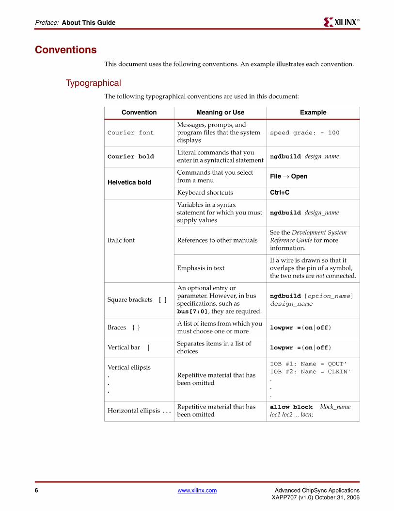
ConventionsThis document uses the following conventions. An example illustrates each convention.
TypographicalThe following typographical conventions are used in this document:
Convention Meaning or Use Example
Courier fontMessages, prompts, and program files that the system displays
speed grade: - 100
Courier boldLiteral commands that you enter in a syntactical statement ngdbuild design_name
Helvetica bold
Commands that you select from a menu File → Open
Keyboard shortcuts Ctrl+C
Italic font
Variables in a syntax statement for which you must supply values
ngdbuild design_name
References to other manualsSee the Development System Reference Guide for more information.
Emphasis in textIf a wire is drawn so that it overlaps the pin of a symbol, the two nets are not connected.
Square brackets [ ]
An optional entry or parameter. However, in bus specifications, such as bus[7:0], they are required.
ngdbuild [option_name] design_name
Braces { } A list of items from which you must choose one or more lowpwr ={on|off}
Vertical bar | Separates items in a list of choices lowpwr ={on|off}
Vertical ellipsis...
Repetitive material that has been omitted
IOB #1: Name = QOUT’ IOB #2: Name = CLKIN’...
Horizontal ellipsis . . . Repetitive material that has been omitted
allow block block_name loc1 loc2 ... locn;
Advanced ChipSync Applications www.xilinx.com 7XAPP707 (v1.0) October 31, 2006
ConventionsR
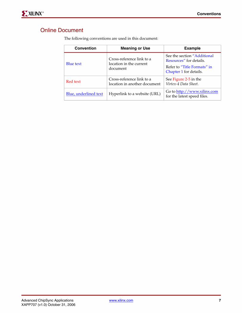
Online DocumentThe following conventions are used in this document:
Convention Meaning or Use Example
Blue textCross-reference link to a location in the current document
See the section “Additional Resources” for details.
Refer to “Title Formats” in Chapter 1 for details.
Red text Cross-reference link to a location in another document
See Figure 2-5 in the Virtex-4 Data Sheet.
Blue, underlined text Hyperlink to a website (URL) Go to http://www.xilinx.com for the latest speed files.

8 www.xilinx.com Advanced ChipSync ApplicationsXAPP707 (v1.0) October 31, 2006
Preface: About This GuideR

Advanced ChipSync Applications www.xilinx.com 9XAPP707 (v1.0) October 31, 2006
R
Chapter 1
Introduction
ChipSync OverviewEvery I/O in every Virtex™-4 device contains ChipSync™ technology. The ChipSync technology includes three basic components: a transmitter, a receiver, and high-speed clocking. Virtex-4 FPGAs contain an OSERDES transmitter, an ISERDES receiver, and a clocking network with I/O clocks and regional clocks. In Figure 1-1, the various ChipSync components are shown as part of the SelectIO™ block.
ChipSync ApplicationsSource-synchronous design techniques are commonly used methods of data transfer among high-speed devices. Common LVDS standards such as SerDes Framer Interface 4.1 (SFI-4.1) and System Packet Interface 4.2 (SPI-4.2) are often used in source-synchronous networking applications. For memory applications, source-synchronous design techniques also allow designers to achieve high performance in DDR2 SDRAM, DDR SDRAM, and QDRII SRAM, among other standards.
One of the most difficult aspects of building a source-synchronous interface is managing setup and hold times. There are many elements in the clock and datapaths, including those from the transmitting device, the receiving device, and the PCB board. These elements must be understood across all specified temperatures, voltages, and process variations. Setup and hold times are derived from this information and often become very complicated and inaccurate calculations.
Figure 1-1: ChipSync Technology Block Diagram
X707_01_01_091905
SelectIO Block
Virtex-4 FPGA
ISERDES- Frequency Division- Bit and Word Alignment
Clocking- I/O Clocks- Regional Clocks- Clock-Capable I/Os
OSERDES- Frequency Multiplication
ChipSync Block

10 www.xilinx.com Advanced ChipSync ApplicationsXAPP707 (v1.0) October 31, 2006
Chapter 1: IntroductionR
ChipSync technology was designed specifically to address this difficulty. The ISERDES contains an IDELAY block that allows the designer to create unique setup and hold timing rather than struggle through various calculations. Using IDELAY, the clock and/or data delay can be accurately adjusted to align the sampling point to the center of the data eye. This process is known as dynamic alignment. The IDELAY block is an important aspect of ChipSync technology, and its operation is discussed in detail in Chapter 2.
Dynamic alignment is the recommended method for all source-synchronous applications. However, static alignment is also a valid method, and it is considered extensively in Chapter 3. By using DS302:Virtex-4 Data Sheet and timing analysis tools, setup and hold timing can be predicted for a specific design. These predictions are then compared to the timing of the actual design measured on a Virtex-4 device.
These source-synchronous interfaces are generally part of a larger system. While the interfaces run on the ChipSync clock domains (I/O and regional), the rest of the system runs on the global clock domain. Because I/O and regional clock networks are a new Virtex-4 feature, Chapter 4 is dedicated to the operation and performance of these clock networks, including a discussion on managing multiple clock domains.
Characterization ResourcesBecause this document is dedicated primarily to comparing theory to measurements, the source listings of all design files used to produce the results in this document are included in the appendixes. These files are intended to assist designers in achieving predictable results.

Advanced ChipSync Applications www.xilinx.com 11XAPP707 (v1.0) October 31, 2006
R
Chapter 2
IDELAY Block Operation
This chapter contains the following sections:
• “Degradation in the IDELAY Tap Chain”
• “Jitter Transfer of IDELAYCTRL Reference Clock”
• “Alternate Reference Clock Frequencies to IDELAYCTRL”
• “Tap Delay Values”
IDELAY is a programmable delay element with a fixed tap resolution of 75 ps, guaranteed over temperature, voltage, and process. Every ISERDES has an IDELAY element. Figure 2-1 is a simplified diagram of the IDELAY block. There is a single input and output for data, as well as several control signals, used to control the programmable delay. The input data travels through a 64-tap delay line, creating 64 copies of the input data, each of which is delayed 75 ps from the previous copy. Based on the control signals, one of the 64 taps is selected as the output data. Therefore, the output data is basically a copy of the input data, delayed by a programmed amount.
The IDELAYCTRL module (also shown in Figure 2-1) is always instantiated with an IDELAY element to guarantee a normalized delay value for the tap chain.
While conventional logic delays vary significantly with temperature, voltage, and processing differences, the delay through the IDELAY chain of 64 buffers is kept constant with the help of a 200 MHz (nominal) oscillator. This oscillator feeds an additional 64-tap delay line that is invisible to the user. A phase comparator compares the output of this
Figure 2-1: IDELAY Block Diagram
IDELAY
I O
C
T0
CE
Data Input
Tap 0 Tap 1 Tap 62 Tap 63
INC
INCCE
RST
RST
C
IDLYCTRL
RST RDY
REFCLK
T0
Data Output
Logic
X707_02_01_091905
12 www.xilinx.com Advanced ChipSync ApplicationsXAPP707 (v1.0) October 31, 2006
Chapter 2: IDELAY Block OperationR
delay line against its input. When the through delay differs from a period of the clock (nominally 5 ns), the output of the phase comparator changes the supply voltage of all associated IDELAY circuits making the through delay equal to one clock period. This phase-locked loop has a naturally slow response time and therefore suppresses any oscillator frequency jitter.
As a result, IDELAY is not affected by temperature, voltage, processing differences, and also by clock jitter, as demonstrated in the “Jitter Transfer of IDELAYCTRL Reference Clock” section.
Figure 2-1 represents a very idealized view of the operation of IDELAY. It says nothing about the impact of the tap chain on the signal integrity of the data, and nothing about the accuracy of the 75 ps delay values. This chapter explores these aspects of the IDELAY operation and verifies the theoretical expectation of the IDELAYCTRL block.
Degradation in the IDELAY Tap ChainLike any element in the series path of a signal, the IDELAY tap chain is not lossless. In every tap, the data signal accumulates a certain amount of random jitter. The degradation also varies for different data patterns. Data with long strings of ones and zeros are degraded more than data with frequent transitions. This degradation is due to pattern jitter, which is deterministic. This section discusses how to determine the amount of degradation per delay tap and provides recommendations for using the IDELAY tap chain.
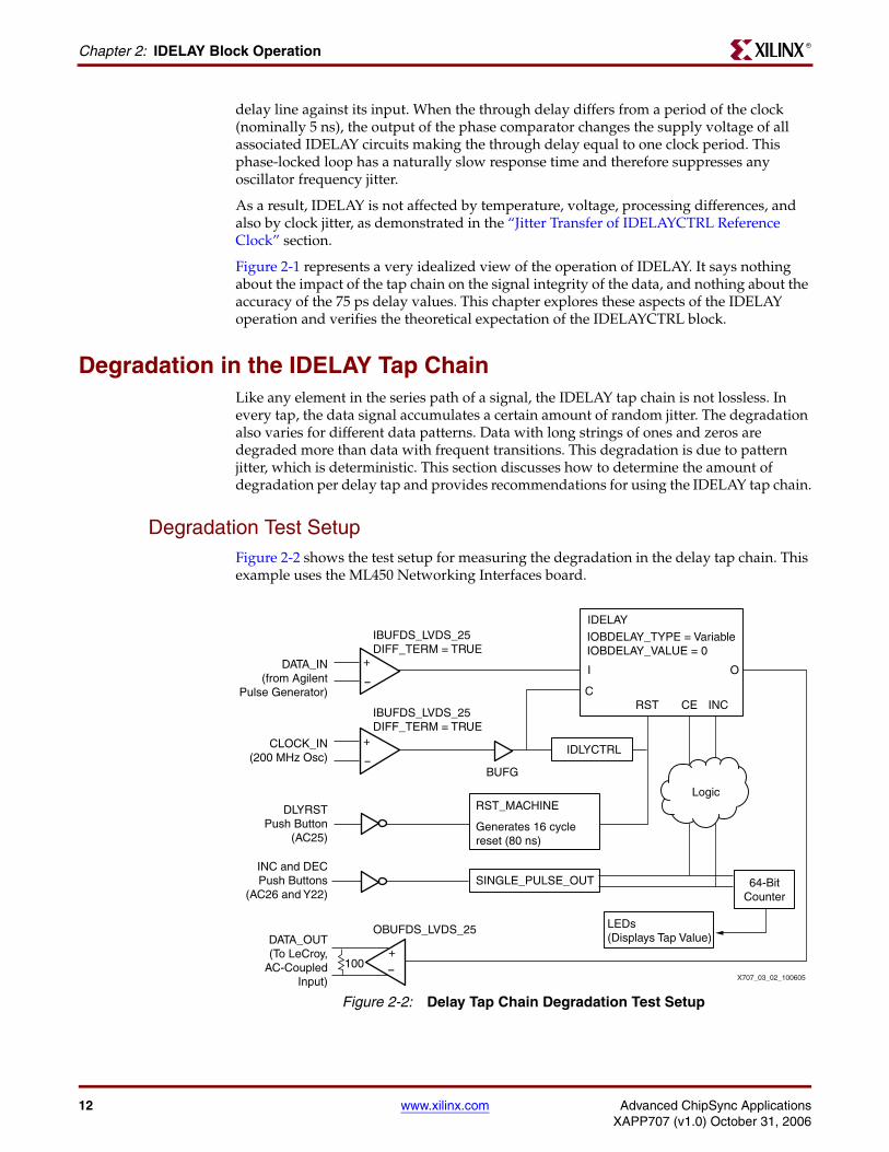
Degradation Test SetupFigure 2-2 shows the test setup for measuring the degradation in the delay tap chain. This example uses the ML450 Networking Interfaces board.
Figure 2-2: Delay Tap Chain Degradation Test Setup
IDELAY
IOBDELAY_TYPE = VariableIOBDELAY_VALUE = 0
BUFG
IBUFDS_LVDS_25DIFF_TERM = TRUE
IBUFDS_LVDS_25DIFF_TERM = TRUE
OBUFDS_LVDS_25
CLOCK_IN(200 MHz Osc)
INC and DECPush Buttons
(AC26 and Y22)
DATA_OUT(To LeCroy,
AC-CoupledInput)
DLYRSTPush Button
(AC25)
IDLYCTRL
LEDs(Displays Tap Value)
SINGLE_PULSE_OUT
RST_MACHINE
Generates 16 cyclereset (80 ns)
64-BitCounter
I O
CCE INCRST
Logic
X707_03_02_100605
+
-
+
-100
DATA_IN(from Agilent
Pulse Generator)
+
-

Advanced ChipSync Applications www.xilinx.com 13XAPP707 (v1.0) October 31, 2006
Degradation in the IDELAY Tap ChainR
The top of Figure 2-2 shows an LVDS data input from an external pattern generator (Agilent 8133A, 3 GHz Pulse Generator). The data input amplitude is 600 mV, and the voltage offset is 1.2V. The LVDS input buffer within the FPGA is programmed to terminate the signal with a 100Ω resistor between the two differential inputs. SMA connectors are used for the board connections.
The data input is routed directly to an IDELAY element. From the IDELAY element, the data is routed to an LVDS output buffer. The signal is differentially terminated on the board at the SMA connectors. From the SMA connectors, the signal is routed to an oscilloscope (LeCroy Serial Data Analyzer SDA6020, 20 GS/s) for a high-precision analysis of signal quality. DC blocks at the inputs of the oscilloscope remove the LVDS offset voltage.
Apart from the data input and output of IDELAY, the control signals must be user-accessible from the board level. Pushbutton switches and LEDs are the only user interface. Because greater precision is required than the unpredictable response of a mechanical switch to reset IDELAY, the RST_MACHINE circuit generates a 16-cycle reset state when the push button is pressed. This circuit guarantees a reset of 80 ns, meeting the 50 ns reset requirement of IDELAYCTRL.
Two push buttons are provided to increment or decrement through the delay tap chain, effectively increasing or decreasing the delay of the data output. A circuit within the design takes the unpredictable response of the mechanical switches and produces single pulses that are routed to the IDELAY control inputs INC and CE. Some logic is required to translate the increment and decrement commands to INC and CE. Table 2-1 shows the operation of INC and CE.
Every time the IDELAY block receives a command to increment or decrement the delay, another circuit also receives the command. This circuit keeps track of the current location in the tap chain and displays that location as a six-digit binary number on the board’s LEDs (LED1 through LED6), where LED1 is the least significant digit.
A 200 MHz clock is required as a reference to the IDELAYCTRL module. This clock is supplied by an oscillator on the board, received by an LVDS input buffer, and distributed on a global clock network. It is also used as the clock input to the IDELAY primitive. The IDELAY clock is used only to synchronize the control inputs. There is no interaction between the IDELAY clock input and the data passing through the IDELAY tap chain. Therefore, the frequency and phase of the test data has no relationship to the 200 MHz clock.
There are several controls and flags not shown in Figure 2-2. Switches 4 and 5 on the board control the VCCINT voltage supplied to the FPGA. By pressing switch 4, the nominal 1.2V internal supply voltage is reduced by 5% to 1.14V. By pressing switch 5, the nominal 1.2V internal supply voltage is increased by 5% to 1.26V. These controls are useful for testing across all operating conditions.
Table 2-1: CE and INC Truth Table Operation
CE INC Operation
0 0 No change
0 1 No change
1 0 Decrement delay
1 1 Increment delay

14 www.xilinx.com Advanced ChipSync ApplicationsXAPP707 (v1.0) October 31, 2006
Chapter 2: IDELAY Block OperationR
Finally, the RDY output of the IDELAYCTRL primitive (not shown in Figure 2-2) is routed to the SM1 LED on the board. This LED is turned on when the RDY output is asserted. If this LED is not active, no measurements should be taken, because the circuit controlling the delay values of the tap chain is not locked.
Advanced ChipSync Applications www.xilinx.com 15XAPP707 (v1.0) October 31, 2006
Degradation in the IDELAY Tap ChainR
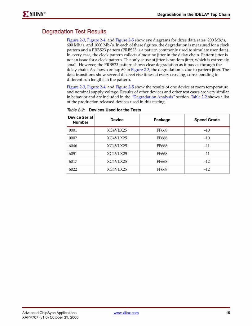
Degradation Test ResultsFigure 2-3, Figure 2-4, and Figure 2-5 show eye diagrams for three data rates: 200 Mb/s, 600 Mb/s, and 1000 Mb/s. In each of these figures, the degradation is measured for a clock pattern and a PRBS23 pattern (PRBS23 is a pattern commonly used to simulate user data). In every case, the clock pattern collects almost no jitter in the delay chain. Pattern jitter is not an issue for a clock pattern. The only cause of jitter is random jitter, which is extremely small. However, the PRBS23 pattern shows clear degradation as it passes through the delay chain. As shown on tap 60 in Figure 2-3, the degradation is due to pattern jitter. The data transitions show several discreet rise times at every crossing, corresponding to different run lengths in the pattern.
Figure 2-3, Figure 2-4, and Figure 2-5 show the results of one device at room temperature and nominal supply voltage. Results of other devices and other test cases are very similar in behavior and are included in the “Degradation Analysis” section. Table 2-2 shows a list of the production released devices used in this testing.
Table 2-2: Devices Used for the Tests
Device Serial Number
Device Package Speed Grade
0001 XC4VLX25 FF668 -10
0002 XC4VLX25 FF668 -10
6046 XC4VLX25 FF668 -11
6051 XC4VLX25 FF668 -11
6017 XC4VLX25 FF668 -12
6022 XC4VLX25 FF668 -12

16 www.xilinx.com Advanced ChipSync ApplicationsXAPP707 (v1.0) October 31, 2006
Chapter 2: IDELAY Block OperationR
Figure 2-3 shows degradation at various points in the delay tap chain for 200 Mb/s data. The test case is using device serial number 6046, -11 speed grade, 25°C, nominal supply voltage.
Figure 2-4 shows degradation at various points in the delay tap chain for 600 Mb/s data. The test case uses device serial number 6046, -11 speed grade, 25°C, nominal supply voltage.
Figure 2-3: Degradation Test Results at 200 Mb/s
Tap00
Eye Width = 4.920 ns
200 Mb/s Data:CLK Pattern
200 Mb/s Data:PRBS23 Pattern
Eye Width = 4.906 ns
Eye Width = 4.674 nsEye Width = 4.932 ns
Eye Width = 4.925 ns Eye Width = 4.447 ns
Eye Width = 4.307 nsEye Width = 4.896 ns
X707_04_03_092005
Tap20
Tap40
Tap60

Advanced ChipSync Applications www.xilinx.com 17XAPP707 (v1.0) October 31, 2006
Degradation in the IDELAY Tap ChainR
Figure 2-4: Degradation Test Results at 600 Mb/s
Tap00
Eye Width = 1.604 ns
600 Mb/s Data:CLK Pattern
600 Mb/s Data:PRBS23 Pattern
Eye Width = 1.539 ns
Eye Width = 1.438 nsEye Width = 1.612 ns
Eye Width = 1.611 ns Eye Width = 1.304 ns
Eye Width = 1.097 nsEye Width = 1.612 ns
X707_05_04_092005
Tap10
Tap20
Tap40

18 www.xilinx.com Advanced ChipSync ApplicationsXAPP707 (v1.0) October 31, 2006
Chapter 2: IDELAY Block OperationR
Figure 2-5 shows degradation at various points in the delay tap chain for 1000 Mb/s data. The test case is using device serial number 6046, -11 speed grade, 25°C, nominal supply voltage.
Figure 2-5: Degradation Test Results at 1000 Mb/s
Tap00
Eye Width = 0.948 ns
1000 Mb/s Data:CLK Pattern
1000 Mb/s Data:PRBS23 Pattern
Eye Width = 0.811 ns
Eye Width = 0.771 nsEye Width = 0.950 ns
Eye Width = 0.948 ns Eye Width = 0.743 ns
Eye Width = 0.629 nsEye Width = 0.948 ns
X707_06_05_092005
Tap05
Tap10
Tap20

Advanced ChipSync Applications www.xilinx.com 19XAPP707 (v1.0) October 31, 2006
Degradation in the IDELAY Tap ChainR
Degradation AnalysisFrom the “Degradation Test Results” section, the data dependence of the degradation in the delay chain is evident. The results for a clock pattern and the results for a PRBS23 pattern are extremely different. No significant degradation in the IDELAY tap chain occurs if the data is a clock pattern. This case is true for all data rates, temperatures, supply voltages, and speed grades. The degradation of a clock pattern in the tap chain is ~0.0 ps/tap. However, the degradation of a PRBS23 pattern is significant and requires further analysis to quantify.
A few of the eye diagrams captured during the characterization process were shown in “Degradation Test Results.” Using similar data for six different devices, eye width can be analyzed as a function of delay taps for a PRBS23 pattern. The slope of the eye width graph is the amount of degradation (pattern jitter) per tap. The graphs for 200 Mb/s, 600 Mb/s, and 1000 Mb/s are included in Appendix B, “IDELAY Degradation Supplemental Data.” The data from those graphs is summarized in Table 2-3. For 1000 Mb/s data, there are two columns shown for each device: one for nominal conditions and one for marginalized supply voltage at +85°C.
Degradation is measured in terms of picoseconds of pattern jitter caused by a single tap in the chain. These numbers are closely correlated to the data pattern, which is PRBS23.
The degradation measurements do not differ significantly for different speed grades or data rates. The measurements are also not significantly worse under worst-case conditions of temperature and voltage. This consistent behavior makes it possible to develop a “rule of thumb” estimate for degradation in the tap chain that is independent of data rate, speed grade, temperature, and voltage.
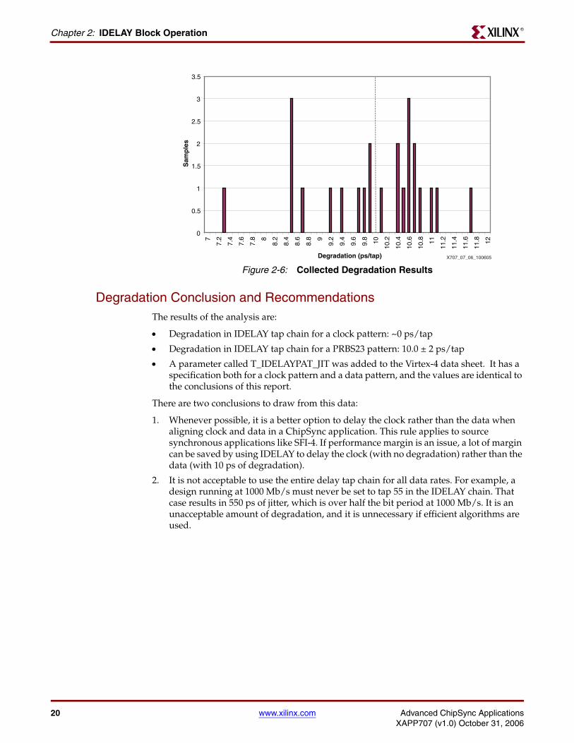
The results from Table 2-3 are collected into a histogram in Figure 2-6. From the histogram, the center of the distribution lies at 10.0 ps/tap of degradation. For a 95% confidence interval, the degradation in the tap chain is 10.0 ± 2 ps/tap for all data rates and speed grades. This value applies specifically to a PRBS23 pattern, which is a common simulation of actual user data.
Table 2-3: Degradation of Data Signals in the IDELAY Tap Chain
Device Serial
NumberSpeed
200 Mb/s Degradation
(ps/tap)
600 Mb/s Degradation
(ps/tap)
1000 Mb/s Degradation
(ps/tap)
1000 Mb/s +85°C
VINT -5%
0001 -10 10.7 10.6 8.4 8.3
0002 -10 10.5 10.4 7.3 8.4
6046 -11 10.7 10.6 9.6 9.8
6051 -11 11.0 10.8 9.7 9.8
6017 -12 11.7 11.1 9.3 10.1
6022 -12 10.4 10.6 8.6 9.1
20 www.xilinx.com Advanced ChipSync ApplicationsXAPP707 (v1.0) October 31, 2006
Chapter 2: IDELAY Block OperationR
Degradation Conclusion and RecommendationsThe results of the analysis are:
• Degradation in IDELAY tap chain for a clock pattern: ~0 ps/tap
• Degradation in IDELAY tap chain for a PRBS23 pattern: 10.0 ± 2 ps/tap
• A parameter called T_IDELAYPAT_JIT was added to the Virtex-4 data sheet. It has a specification both for a clock pattern and a data pattern, and the values are identical to the conclusions of this report.
There are two conclusions to draw from this data:
1. Whenever possible, it is a better option to delay the clock rather than the data when aligning clock and data in a ChipSync application. This rule applies to source synchronous applications like SFI-4. If performance margin is an issue, a lot of margin can be saved by using IDELAY to delay the clock (with no degradation) rather than the data (with 10 ps of degradation).
2. It is not acceptable to use the entire delay tap chain for all data rates. For example, a design running at 1000 Mb/s must never be set to tap 55 in the IDELAY chain. That case results in 550 ps of jitter, which is over half the bit period at 1000 Mb/s. It is an unacceptable amount of degradation, and it is unnecessary if efficient algorithms are used.
Figure 2-6: Collected Degradation Results
0
0.5
1
1.5
2
2.5
3
3.5
7
7.2
7.4
7.6
7.8 8
8.2
8.4
8.6
8.8 9
9.2
9.4
9.6
9.8 10
10.2
10.4
10.6
10.8 11
11.2
11.4
11.6
11.8 12
Degradation (ps/tap)
Sam
ple
s
X707_07_06_100605

Advanced ChipSync Applications www.xilinx.com 21XAPP707 (v1.0) October 31, 2006
Degradation in the IDELAY Tap ChainR
Figure 2-7 shows the recommendation for delay tap usage. The graph assumes that an algorithm aligning clock and data channels requires no more than 1.5 bit times of delay, where the proof is that data can have any relationship to the clock upon arrival to the pins of an ISERDES. Figure 2-8(a) shows the worst-case starting point of an algorithm designed to delay the data until the center of the data eye is aligned to the rising edge of the clock. It is the case where the clock's rising edge occurs immediately before the data transition. Because an algorithm cannot determine the center of a data eye without finding both edges of the eye, the first eye must be sacrificed and the second eye used. Therefore, the algorithm uses ~1 bit time to discard the first data eye and another 0.5 bit times to get to the center of the second data eye, as shown in Figure 2-8(b). All other cases require less than 1.5 bit times.
Figure 2-7: Recommendation for Maximum Delay Tap Usage at Specific Data Rates
Figure 2-8: Worst-Case Clock-Data Relationship for an Algorithm that Aligns Center of Data to the Rising Edge of the Clock
X707_08_07_100305
0
10
20
30
40
50
60
70
200 300 400 500 600 700 800 900 1000 1100 1200
Data Rate (Mbit/s)
Max
Del
ay T
aps
Delay tap usage must fall below this line to guarantee that no more than 20% of data bit period is lost to degradation in the tap chain.
(a)Before
Alignment
Data D2 D1 D0
D3 D2 D1
Clock
Clock
Data(b)After
Alignment
X707_09_08_092005

22 www.xilinx.com Advanced ChipSync ApplicationsXAPP707 (v1.0) October 31, 2006
Chapter 2: IDELAY Block OperationR
To determine 1.5 bit periods in terms of taps (as shown in Figure 2-7), the bit period of the data rate is calculated and divided by 75 to obtain the bit period in terms of taps. For 1000 Mb/s:
• One bit period = 1/1000 = 1.0 ns
• 1.5 bit periods = 1.0 + 0.5 = 1.5 ns
• Maximum taps = 1500 / 75 ps = 20 taps
Jitter Transfer of IDELAYCTRL Reference ClockAnother signal quality concern is the jitter transfer of the 200 MHz reference clock to the data in the IDELAY chain. The reference clock drives the temperature compensation circuit (IDELAYCTRL) that maintains constant delay values in the tap chain over temperature and process. This control circuit operates in real-time and has a finite jitter transfer characteristic to the data signal. The expectation of the circuit is that the jitter transfer is close to zero. Random and deterministic jitters are considered in separate cases.
Jitter transfer of the reference clock is important because designers often do not want to include a 200 MHz oscillator on the board just to drive the IDELAYCTRL circuit. To save resources, designers prefer to use a DCM to multiply or divide any clock available to generate a 200 MHz clock. However, the DCM multiplier output (CLKFX) has more jitter than a clean oscillator output. For this reason, it is necessary to understand the signal quality impact of using the DCM to generate the 200 MHz reference clock.
Jitter Transfer Test Setup Figure 2-9 shows the test setup for measuring the jitter transfer of the 200 MHz reference clock to the data signal in the IDELAY chain. It is designed for the ML450 Networking Interfaces board.

Advanced ChipSync Applications www.xilinx.com 23XAPP707 (v1.0) October 31, 2006
Jitter Transfer of IDELAYCTRL Reference ClockR
There are two important signals that must be monitored: the reference clock and the data in the IDELAY chain. At the top of Figure 2-9, there is an LVDS data input from an external pattern generator (Agilent 8133A, 3 GHz Pulse Generator). The data input amplitude is 600 mV and the voltage offset is 1.2V. The LVDS input buffer within the FPGA is programmed to terminate the signal with a 100Ω resistor between the two differential inputs. The physical connections on the board are SMA connectors.
The data input is routed directly to an IDELAY block. From the IDELAY block, the data is routed to an LVDS output buffer. The signal is differentially terminated at the SMA connectors on the board. From the SMA connectors, the signal is routed to an oscilloscope (LeCroy Serial Data Analyzer SDA6020, 20 GS/s) where it is analyzed to high precision for signal quality. There are DC blocks at the inputs of the oscilloscope to remove the LVDS offset voltage.
The “Degradation in the IDELAY Tap Chain” section states that a clock pattern gathers no pattern jitter in the delay chain. Because of this, a clock pattern is used for jitter transfer measurements to separate the effects of pattern jitter from jitter transfer.
A 200 MHz clock is required as a reference to the IDELAYCTRL block. This clock is supplied by an oscillator on the board, received by an LVDS input buffer, and distributed on a global clock multiplexer network. The clock supplied to the IDELAYCTRL block either comes directly from the oscillator or from a DCM. The clock is selectable using switch 6 on the board (pressing the button selects the DCM clock). The 200 MHz reference clock is also used as the clock input to the IDELAY block. The IDELAY clock is used only to synchronize the control inputs. There is no interaction between the IDELAY clock input and the data passing through the IDELAY tap chain. Therefore, the frequency and phase of the test data have no relationship to the 200 MHz clock.
Figure 2-9: Test Setup for Measuring Jitter Transfer of the 200 MHz Reference Clock
IDELAY
IOBDELAY_TYPE = VariableIOBDELAY_VALUE = 0
BUFGMUX
IBUFDS_LVDS_25DIFF_TERM = TRUE
IBUFDS_LVDS_25DIFF_TERM = TRUE
OBUFDS_LVDS_25
CLOCK_IN(200 MHz Osc)
INC and DECPush Buttons
(AC26 and Y22)
DATA_OUT(To LeCroy,
AC-CoupledInput)
DLYRSTPush Button
(AC25)
IDLYCTRLDCM
LEDs(Displays Tap Value)
SINGLE_PULSE_OUT
RST_MACHINE
Generates 16 cyclereset (80 ns)
64-BitCounter
I O
CCE INCRST
Logic
X707_03_02_100605
+
-
+
-100
DATA_IN(from Agilent
Pulse Generator)
+
-
OBUFDS_LVDS_25CLOCK_OUT
(To LeCroy,AC-Coupled
Input)
+
-100

24 www.xilinx.com Advanced ChipSync ApplicationsXAPP707 (v1.0) October 31, 2006
Chapter 2: IDELAY Block OperationR
Apart from the data input and output of the IDELAY block, the control signals must be user-accessible from the board level. Push buttons and LEDs provide the only user interface. To reset the IDELAY block, a greater precision is required than the unpredictable response of a mechanical switch. A circuit called RST_MACHINE generates a 16-cycle reset state when the push button is pressed. This circuit guarantees a reset of 80 ns, which meets the 50 ns reset requirement of IDELAYCTRL.
There are several controls and flags not shown in Figure 2-9. Switches 4 and 5 on the board control the VCCINT voltage supplied to the FPGA. By pressing switch 4, the nominal 1.2V internal supply voltage is reduced by 5% to 1.14V. By pressing switch 5, the nominal 1.2V internal supply voltage is increased by 5% to 1.26V. These controls are useful for conducting a test across all operating conditions.
Finally, the RDY output of the IDELAYCTRL block (not shown in Figure 2-9) is routed to LED “SM1” on the board. This LED turns on when the RDY output is asserted. No measurements must be taken if this LED is not active. It means that the circuit controlling the delay values of the tap chain is not locked.
Jitter Transfer Test ResultsTo measure the transfer of random jitter, the CLK0 pin of the DCM drives the IDELAYCTRL block, and the phase setting is set to 1024. The “clean” oscillator clock goes through 1,024 circuit elements in the DCM, and each element adds a small amount of random jitter to the output clock. Both the clean case and the jittered case are shown in Figure 2-10, along with the corresponding data signals. The data signal quality is visibly unaffected by a large increase in random jitter on the IDELAYCTRL reference clock. Random jitter on the 200 MHz reference clock to IDELAYCTRL does not transfer to data signals in the IDELAY tap chain. The CLK0 pin of the DCM when used with a phase shift setting of 1024 creates maximum random jitter.
Figure 2-10: Random Jitter Transfer of the 200 MHz Reference Clock
X707_11_10_092005

Advanced ChipSync Applications www.xilinx.com 25XAPP707 (v1.0) October 31, 2006
Alternate Reference Clock Frequencies to IDELAYCTRLR
In Figure 2-11, the deterministic jitter transfer is also measured by using the DCM. The CLKFX output of the DCM drives the IDELAYCTRL reference clock. The multiply factor is set to 20 and the divide factor is also set to 20, yielding a 200 MHz output with a large amount of deterministic jitter. Comparing the data signal quality in the two cases of Figure 2-11 shows that data signal quality is visibly unaffected by a large increase in deterministic jitter on the IDELAYCTRL reference clock. The deterministic jitter on the 200 MHz reference clock to IDELAYCTRL does not transfer to the data signals in the IDELAY tap chain.
The same observations were true when the VCCINT supply was margined to -5% of its nominal value. The same observations were also true when the temperature was +85°C.
The data from Figure 2-10 and Figure 2-11 is measured in a -10 speed grade device (device serial number 0002). The same test was repeated using a -12 device (device serial number 6022), and the results were the same. See Table 2-2 for more information about these devices.
Jitter Transfer ConclusionThe amount of jitter transfer from the IDELAYCTRL 200 MHz reference clock to the data signal in the IDELAY chain is too small to quantify. The jitter transfer is ~0. Because the jitter tolerance is so low, the CLKFX output of a DCM can be used in any configuration to generate the 200 MHz reference clock.
Alternate Reference Clock Frequencies to IDELAYCTRLThe reference clock to the IDELAYCTRL block is specified as 200 MHz. The purpose of this section is to characterize the behavior of the IDELAY and IDELAYCTRL blocks when the reference clock is changed to frequencies other than 200 MHz.
Figure 2-11: Deterministic Jitter Transfer of the 200 MHz Reference Clock
X707_12_11_092005
26 www.xilinx.com Advanced ChipSync ApplicationsXAPP707 (v1.0) October 31, 2006
Chapter 2: IDELAY Block OperationR
Different reference clock frequencies produce different delays in the IDELAY tap chain. At 200 MHz, the delay is known to be 75 ps. Other frequencies produce a different result.
The reference clock is not optional to connect. If no clock is connected to IDELAYCTRL, then the data output of the IDELAY block remains in a Low state, and the READY output of the IDELAYCTRL block remains deasserted. A deasserted READY signal indicates that the delay values of the tap chain are unpredictable and undefined.
Alternate REFCLK Test SetupThe test setup for characterizing various reference clock frequencies is the same as the setup in Figure 2-2, except the reference clock input comes from a pulse generator rather than an oscillator. Use of the pulse generator allows manipulation of the frequency. The setup is designed for the ML450 Networking Interfaces board.
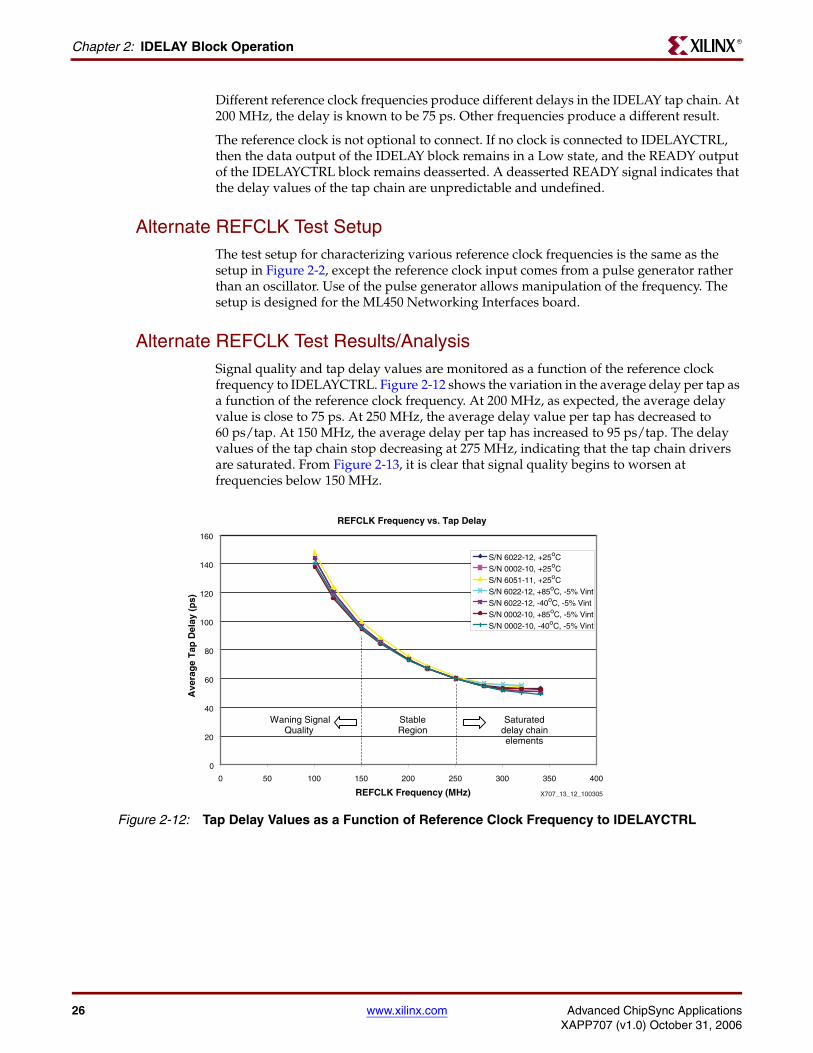
Alternate REFCLK Test Results/AnalysisSignal quality and tap delay values are monitored as a function of the reference clock frequency to IDELAYCTRL. Figure 2-12 shows the variation in the average delay per tap as a function of the reference clock frequency. At 200 MHz, as expected, the average delay value is close to 75 ps. At 250 MHz, the average delay value per tap has decreased to 60 ps/tap. At 150 MHz, the average delay per tap has increased to 95 ps/tap. The delay values of the tap chain stop decreasing at 275 MHz, indicating that the tap chain drivers are saturated. From Figure 2-13, it is clear that signal quality begins to worsen at frequencies below 150 MHz.
Figure 2-12: Tap Delay Values as a Function of Reference Clock Frequency to IDELAYCTRL
REFCLK Frequency vs. Tap Delay
0
20
40
60
80
100
120
140
160
0 50 100 150 200 250 300 350 400
REFCLK Frequency (MHz)
Ave
rag
e T
ap D
elay
(p
s)
S/N 6022-12, +25oCS/N 0002-10, +25oCS/N 6051-11, +25oCS/N 6022-12, +85oC, -5% VintS/N 6022-12, -40oC, -5% VintS/N 0002-10, +85oC, -5% VintS/N 0002-10, -40oC, -5% Vint
Saturated delay chain elements
Waning Signal Quality
Stable Region
X707_13_12_100305

Advanced ChipSync Applications www.xilinx.com 27XAPP707 (v1.0) October 31, 2006
Tap Delay ValuesR
Alternate REFCLK ConclusionsWhen the reference clock is below 150 MHz, the signal quality of the data signal in the IDELAY chain is degraded. When the reference clock is above 275 MHz, the delay chain drivers become saturated and produce inconsistent delay values, as shown in Figure 2-12. In contrast, at 200 MHz, the delay values of all devices at all conditions are very close to one another.
The stable range of operation for the IDELAY chain is between 175 MHz and 225 MHz. The specification in the Virtex-4 Data Sheet shows the range of operation to be 190 MHz to 210 MHz. This is the only range that is guaranteed. The results in this section (“Alternate Reference Clock Frequencies to IDELAYCTRL”) show that there is a comfortable margin around the specification.
Tap Delay ValuesThe delay values of the IDELAY chain are determined by the 200 MHz reference clock to IDELAYCTRL. More accurately, the reference clock determines the delay of the entire tap chain. Thus, the average of all 64 taps in the chain is constrained to 75 ps/tap, but there is no constraint on each individual tap. The purpose of this section is to measure the delay values of every tap in the chain and quantify the accuracy of the delay values.
Tap Delay Measurement Test SetupThe test setup for characterizing tap delay values is the same as the setup in Figure 2-2, page 12. The setup is designed for the ML450 Networking Interfaces board.
A clock pattern from an Agilent pulse generator goes through the IDELAY chain and out again to a LeCroy oscilloscope. A clock pattern is used to avoid the effects of pattern jitter in these measurements. To measure delay, the data delay is calibrated at tap 0 in the delay chain. Because the output signal is AC-coupled, the crossing point of the data transition is recorded at a level of 0 volts. When the tap chain is incremented to tap 1, the crossing point
Figure 2-13: Data Eye Width as a Function of Reference Clock Frequency to IDELAYCTRL
REFCLK Frequency vs. Signal Quality at 1 Gbps
0.7
0.75
0.8
0.85
0.9
0.95
1
0 50 100 150 200 250 300 350 400
REFCLK Frequency (MHz)
Eye
Wid
th (
ns)
S/N 0002-10
S/N 6022-12
S/N 6051-11
S/N 6022-12, 85oC, -5% Vint
S/N 6022-12, -40oC, -5% Vint
S/N 0002-10, 85oC, -5% Vint
S/N 0002-10, -40oC, -5% Vint
Waning Signal Quality
X707_14_13_100305

28 www.xilinx.com Advanced ChipSync ApplicationsXAPP707 (v1.0) October 31, 2006
Chapter 2: IDELAY Block OperationR
of the data is recorded again at a level of 0 volts. The delay value of tap 1 is the difference between the value at tap 1 and tap 0. The delay value of tap 2 is the difference between the value at tap 2 and tap 1. The same measurement is repeated for the entire chain.
Tap Delay Measurement Results/AnalysisFigure 2-14 and Figure 2-15 show the distribution of individual tap delay values for two devices. Although the average tap delay is very close to 75 ps, the actual delay of each individual tap has a wide range of values—a range of ~40 ps. If a designer is “counting taps” to get an accurate estimate of delay (number of taps multiplied by 75 ps), this range can be a source of inaccuracy. However, a closer inspection of the tap delays as they occur in sequence shows that the wide range of delays offset one another, as shown in Table 2-4.
Figure 2-14: Distribution of Tap Delays in 64-Tap Chain for Device 0001-10
X707_15_14_100305
Histogram of Tap Delay Values at 85oC, -5% Vint, SN 0001-10
0
1
2
3
4
5
6
22 26 30 34 38 42 46 50 54 58 62 66 70 74 78 82 86 90 94 98 102
106
Tap Delay Value (ps)
Sam
ple
s
Average Tap Values:
Entire chain: 75.1 ± 0 psEvery 10 taps: 75.1 ± 3 psEvery 05 taps: 75.1 ± 6 psEvery 02 taps: 75.1 ± 12 psSingle Tap: 75.1 ± 21 ps
Average Delay Value: 75.1 ps

Advanced ChipSync Applications www.xilinx.com 29XAPP707 (v1.0) October 31, 2006
Tap Delay ValuesR
For example, the range of delays for each tap is ~40 ps, but the range of delays for any five taps is only ~12 ps. Therefore, a designer who counts 5 taps and assumes that each tap is 75 ps is not wrong by more than ± 6 ps. Figure 2-14 and Figure 2-15 each have a table showing accuracies for various numbers of taps. The two devices represented in Figure 2-14 and Figure 2-15 have similar spreads of delay values. The data presented for the devices is at +85°C with a -5% internal supply voltage. The data collected under nominal conditions is roughly the same for both devices.
For both devices, the delays of tap 1 and tap 63 are anomalies. The tap 1 delay is very small, and the tap 63 delay is very large.
Figure 2-15: Distribution of Tap Delays in 64-Tap Chain for Device 6022-12
Table 2-4: Tap Delay Values for Device 0001-10 at +85°C and -5% VINT
Tap Delay Value Tap Delay Value
00 Baseline 32 67
01 22(1) 33 93
02 85 34 54
03 74 35 72
04 84 36 69
05 67 37 84
06 88 38 68
07 60 39 79
08 81 40 68
09 80 41 73
10 82 42 77
11 59 43 78
X707_16_15_100305
Histogram of Tap Delay Values at 85oC, -5% Vint, SN6022-12
0
1
2
3
4
5
6
39 42 45 48 51 54 57 60 63 66 69 72 75 78 81 84 87 90 93 96 99 102
Tap Delay Value (ps)
Sam
ple
s
Average Tap Values:
Entire chain: 73.4 ± 0 psEvery 10 taps: 73.4 ± 2 psEvery 05 taps: 73.4 ± 5 psEvery 02 taps: 73.4 ± 12 psSingle Tap: 73.4 ± 19 ps
Average Delay Value: 73.4 ps

30 www.xilinx.com Advanced ChipSync ApplicationsXAPP707 (v1.0) October 31, 2006
Chapter 2: IDELAY Block OperationR
Tap Delay Conclusion and RecommendationDelay values of individual taps in the IDELAY tap chain are not guaranteed to be 75 ps. The average delay through the entire chain is guaranteed to be 75 ps (with slight variation).
When dynamic alignment is used to control the delay elements, the actual delay values of the taps are not important. The dynamic scheme automatically customizes the final setting to the specific delays of any device. When static alignment is used and the designer needs to compute “on paper” the expected delays in the system, the parameter T_IDELAYTOTAL_ERR in the Virtex-4 data sheet can be used to account for inaccuracy in the tap chain. The equation for T_IDELAYTOTAL_ERR is shown in Equation 2-1. The constant factor of 34 ps accounts for the first tap, which is always abnormally small. The average value of many measurements of the first tap on many devices is 34. Equation 2-1 is valid from Tap 1 to Tap 63.
Equation 2-1
12 80 44 68
13 78 45 95
14 75 46 68
15 81 47 87
16 76 48 81
17 70 49 71
18 73 50 64
19 82 51 90
20 75 52 65
21 67 53 83
22 78 54 59
23 80 55 81
24 72 56 86
25 77 57 74
26 77 58 68
27 72 59 82
28 75 60 84
29 85 61 62
30 70 62 70
31 83 63 107(1)
Notes: 1. The first and last taps in the tap chain are anomalies. First tap is far below average and last tap is far
above average.
Table 2-4: Tap Delay Values for Device 0001-10 at +85°C and -5% VINT (Continued)
Tap Delay Value Tap Delay Value
TIDELAYTOTAL_ERR [(tap 1) 74 34] 0.07[(tap – 1) 74 34 ]+×±+×–=
Advanced ChipSync Applications www.xilinx.com 31XAPP707 (v1.0) October 31, 2006
Tap Delay ValuesR
For example, a designer determines that a design is using 10 taps to optimize the alignment of clock and data. The designer calculates:
• Total delay estimate: (10-1) x 74 + 34 = 700 ps
• Error: ±0.07 x 700 ps = ±49 ps
• Total delay at tap 10: 700 ± 49 ps
This calculation holds true over PVT and for all speed grades.

32 www.xilinx.com Advanced ChipSync ApplicationsXAPP707 (v1.0) October 31, 2006
Chapter 2: IDELAY Block OperationR

Advanced ChipSync Applications www.xilinx.com 33XAPP707 (v1.0) October 31, 2006
R
Chapter 3
ISERDES Timing
This chapter contains the following sections:
• “Setup and Hold Conventions”
• “Virtex-4 Data Sheet and ISE Timing Analyzer”
• “Signal Integrity and Jitter”
• “Test Case 1: Clock and Datapath with IDELAY”
• “Test Case 2: Datapath with IDELAY”
• “Test Case 3: Data and Clock Path with no IDELAY”
• “Clock-Data Alignment Schemes”
Static timing calculations can easily become very theoretical, inaccurate, and abstracted from actual hardware. The purpose of this chapter is to correlate raw timing calculations to actual hardware. The three primary areas of consideration when evaluating timing are the Virtex-4 Data Sheet (DS302), the software timing analyzer, and hardware measurement. A designer who can correlate these three areas has gained the ability to predict timing with a high degree of confidence.
The scope of the test is simple: a clock channel and a data channel “race” to the ISERDES. The clock and data arrive at the ISERDES with a specific setup and hold relationship that can be optimized using ChipSync features. There are many possible design configurations for the clock and datapaths, and not all of them are included in the Virtex-4 Data Sheet. Two of those configurations are considered in this chapter and verified in hardware.
Setup and Hold ConventionsIn source synchronous designs, the clock and data normally arrive at the receiver input pins phase-matched as closely as possible. The clock and datapaths within the receiver determine setup and hold times.
The setup and hold calculations form a timing window in which the clock and data relationship can lie. The size of this timing window is determined by variations over large amounts of tested devices, over the specified temperature range of the devices, and over the specified voltage range of the devices. These three sources of variation are defined as Process, Temperature, and Voltage (PVT).
All elements in the data and clock path are affected by PVT, including I/O blocks, IDELAY blocks, ISERDES blocks, and routing networks. Each of these elements has worst-case delays and best-case delays over PVT. These numbers are used in the calculation of the setup and hold times of a clock and data signal “racing” to a sampling register (ISERDES).
Equation 3-1 and Equation 3-2 show the setup and hold times, respectively.
Setup Time = Slowest Data Path Delay – Fastest Clock Path Delay Equation 3-1

34 www.xilinx.com Advanced ChipSync ApplicationsXAPP707 (v1.0) October 31, 2006
Chapter 3: ISERDES TimingR
Hold Time = Slowest Clock Path Delay – Fastest Data Path Delay Equation 3-2
To compute the slowest datapath delay, the worst-case delays for every element in the datapath must be summed. To compute the fastest clock path delay, the best-case delays for every element in the clock path must be summed. The absolute minimum amount of time that the data is guaranteed to be stable before the arrival of the clock is derived by subtracting the fastest clock path from the slowest datapath as shown in Equation 3-1. This value is guaranteed over PVT. The hold time is calculated in the same way and is also guaranteed over PVT.
Virtex-4 Data Sheet and ISE Timing AnalyzerWorst-case and best-case delays must be known for all elements in the clock and datapath to accurately calculate setup and hold times. Not all of these delays are provided in the Virtex-4 Data Sheet. Signal nets are dependent on the constraints of specific designs, making it impossible to specify innumerable routing scenarios. For the same reason, package skew cannot be specified in the data sheet for every pin of every device.
It is necessary to run the ISE Timing Analyzer tools in the ISE Software Suite rather than rely only on the data sheet for calculating the setup and hold times of a specific design. The timing analyzer uses the data sheet as a source of information but also has access to timing information more specific to the design in question. The timing analyzer settings are set according to Figure 3-1 to get all the information required for this analysis. These settings cause the analyzer to report all signal paths, regardless of the timing constraints of the design. The ISE version used in this chapter is 7.1 (SP4).
The timing report (*.twr) contains detailed setup and hold calculations for all clock domains. The part of the report relevant to ISERDES timing is labelled as:
============================================================Timing constraint: Unconstrained OFFSET IN BEFORE analysis for clock "RXCLK"
Offset (setup paths): (data path - clock path + uncertainty)...
Figure 3-1: Timing Analyzer Settings
X707_20_04_091905

Advanced ChipSync Applications www.xilinx.com 35XAPP707 (v1.0) October 31, 2006
Virtex-4 Data Sheet and ISE Timing AnalyzerR
Offset (hold paths): (data path - clock path + uncertainty)============================================================

36 www.xilinx.com Advanced ChipSync ApplicationsXAPP707 (v1.0) October 31, 2006
Chapter 3: ISERDES TimingR
Signal Integrity and JitterAssuming that the clock and data signals have no jitter, the maximum frequency is 1/Th, where Th is the calculated hold time. The maximum frequency is limited by the hold time because high frequencies cause the hold edge of the data eye to shrink. When the hold edge of the data eye reaches the calculated hold time, then the clock and data are no longer guaranteed to sample correctly over PVT.
However, signal integrity and jitter are also considerations in the calculation of a timing budget. The maximum frequency is less than 1/Th due to effects that degrade signal integrity. In “Setup and Hold Conventions,” the clock and data transitions were assumed to be perfect. There was no consideration of pattern jitter, jitter from the transmitter and transmission lines, or degradation in the IDELAY chain if it is used (characterized in “Degradation in the IDELAY Tap Chain,” page 12). The Virtex-4 Data Sheet and the timing analyzer cannot account for the inherent jitter of the incoming clock and data signals, and the timing analyzer does not account for degradation in the IDELAY chain. These additional effects widen the setup and hold timing window, as shown in Figure 3-2.
To simplify the testing in this chapter, the effects of jitter and degradation are minimized. The data pattern used in the hardware timing verification is a clock pattern. From Chapter 2, “IDELAY Block Operation,” a clock pattern is known to suffer less than 1 ps of degradation in each tap of the delay chain. Therefore, IDELAY degradation is small enough to ignore in the hardware verification. The input clock and data signals are driven by a high-precision Agilent pulse generator, with less than 10 ps peak-to-peak jitter on the outputs. Therefore, input jitter is also small enough to ignore in the hardware verification.
For the tests in this chapter, the hardware verification includes all of the considerations of setup and hold timing that the timing analyzer includes in its calculation. The hardware results are expected to fall within the limits calculated by the timing analyzer.
Test Case 1: Clock and Datapath with IDELAYFigure 3-3 shows an example configuration of a clock and datapath, containing data and clock paths with IDELAY in variable mode (initialized to tap 0). This configuration is required to delay both clock and data using the 64-tap IDELAY tap chain (discussed in detail in Chapter 2, “IDELAY Block Operation”). The I/O pins are shown at the left of the diagram, and each signal propagates along the signal path from the I/O pins to the ISERDES flip-flops, where the data is sampled by the clock.
Figure 3-2: Actual vs. Calculated Setup and Hold Windows
D0
Actual Setup/Hold Window
Calculated Setup/Hold Window
X707_21_05_091905

Advanced ChipSync Applications www.xilinx.com 37XAPP707 (v1.0) October 31, 2006
Test Case 1: Clock and Datapath with IDELAYR
Theoretical Setup and Hold Calculations of Test Case 1From inspection of Figure 3-3, the clock path is longer than the datapath, because there is an extra element (BUFIO) in the clock path. Therefore, the data is expected to arrive before the clock. To quantify the setup and hold times of this specific configuration, the individual delays in the datapath must be summed and compared to the sum of individual delays of the clock path. Table 3-1 and Table 3-2 shows the descriptions of the individual delays.
Figure 3-3: ISERDES Timing Measurement Scenario
+
–
+
–
DATAPATH
CLOCKPATH
ISERDESFFs
D
CLKBUFIO
IBUFDS
IBUFDS
TIOPI TNET TISDCK_D
TNET1 TNET3TNET2TISDO_DO_IOBDELAY_IBTIOPI
X707_22_06_102605
IDELAY
I O
IDELAY
I O
Table 3-1: Datapath Timing Definitions
Timing Parameter Description
TIOPI Delay from the IOB pad through the LVDS input buffer to the I pin of the IOB pad
TNET Delay from the I pin of the IOB pad to the D input of the Data ISERDES/ILOGIC block
TISDCK_D Delay from the D input of the ISERDES to the D flip-flops in the ISERDES (setup and hold times of ISERDES)
Table 3-2: Clock Path Timing Definitions
Timing Parameter Description
TIOPI Delay from the IOB pad through the LVDS input buffer to the I pin of the IOB pad
TNET1 Delay from the I pin of the IOB pad to the D input of the Clock ISERDES block

38 www.xilinx.com Advanced ChipSync ApplicationsXAPP707 (v1.0) October 31, 2006
Chapter 3: ISERDES TimingR
Each of the parameters in Table 3-1 and Table 3-2 have a best-case and worst-case value over PVT (as discussed in Overview of Setup and Hold Calculations). Net delays are generated by the timing analyzer and not specified in the Virtex-4 Data Sheet because they are specific to this particular design configuration. TIOPI is specified in the Virtex-4 Data Sheet, but the timing analyzer adjusts the data sheet values to account for the effects of package skew in this specific design.
Table 3-3 and Table 3-4 show the values of the delays in the test case in Figure 3-3. The values are extracted directly from the timing report generated by the ISE Timing Analyzer (ISE 7.1 SP4) for a -10 speed grade device. Slowest and fastest paths are determined by summing the individual delay values together. Setup and hold times are calculated from the slowest and fastest paths according to Equation 3-1 and Equation 3-2. See Appendix E, “ISERDES Timing Source Files,” for the actual timing report.
The final calculations are:
• Setup Time: SLOW DATA – FAST CLK = 2.368 – 2.649 = -0.281
• Hold Time: SLOW CLK – FAST DATA = 3.131 – 1.872 = 1.259
TISDO_DO_IOBDELAY_IBUF Delay from the D input of the Clock ISERDES block to the DO output pin of the Clock ISERDES block with IDELAY in the path
TNET2 Delay from the DO output pin of the Clock ISERDES to the I input of BUFIO
TNET3 Delay from the BUFIO I input to the CLK input of Data ISERDES (the BUFIO delay is included in the overall net delay)
Table 3-3: Data Delay Calculation from ISE Timing Analyzer
Parameter Setup Time (SLOW DATA) Hold Time (FAST DATA)
TIOPI 1.350 ns 1.122 ns
TNET 0.117 ns 0.108 ns
TISDCK_D 0.901 ns -0.642 ns
TOTAL 2.368 ns 1.872 ns
Table 3-4: Clock Delay Calculation from ISE Timing Analyzer
Parameter Setup Time (FAST CLK) Hold Time (SLOW CLK)
TIOPI 1.074 ns 1.300 ns
TNET1 0.108 ns 0.117 ns
TISDO_DO_IOBDELAY_IBUF 0.903 ns 0.982 ns
TNET2 0.001 ns 0.001 ns
TNET3 0.563 ns 0.731 ns
TOTAL 2.649 ns 3.131 ns
Table 3-2: Clock Path Timing Definitions (Continued)
Timing Parameter Description

Advanced ChipSync Applications www.xilinx.com 39XAPP707 (v1.0) October 31, 2006
Test Case 1: Clock and Datapath with IDELAYR
• Timing Window: 1.259 – 0.281 = 0.978 ns
The setup time is negative, and the hold time is positive. Assuming that data and clock are phase-aligned (with some tolerance) at the input pins to the FPGA. This design meets timing across PVT for all -10 speed grade devices. Figure 3-4 shows the timing relationship with IDELAY in Variable mode, initialized to tap 0.
The maximum frequency of this example is limited by the hold time of 1.259 ns (794 Mbits), although the actual maximum frequency is lower due to the effects of finite rise and fall times, transmission path loss, and degradation in the IDELAY chain (as discussed in Chapter 2, “IDELAY Block Operation”).
Hardware Verification of Test Case 1The test setup used in the hardware verification is shown in Figure 3-5. It measures the setup and hold times of the data and clock paths with IDELAY in Variable mode, initialized to tap 0. The source code is included in Appendix E, “ISERDES Timing Source Files.” The test setup implements the same clock and datapath, as shown in Figure 3-1, and it provides the ability to control the data delay. To separate the effects of pattern jitter from the timing measurements, the datapath is driven by a 400 Mb/s clock pattern, and the clock path is driven by a clock running at 400 MHz. The data and clock are driven by an external pattern generator (Agilent 8133A, 3 GHz Pulse Generator). The input amplitude is 600 mV, and the voltage offset is 1.2V. The LVDS input buffers within the FPGA are programmed to terminate the signal with a 100Ω resistor between the two differential inputs. The physical connections on the board are SMA connectors.
Figure 3-4: Setup and Hold Times of Clock and Data Channels
D1DATA
CLOCK
1.259 ns
-0.281 ns
D0
X707_23_07_091905

40 www.xilinx.com Advanced ChipSync ApplicationsXAPP707 (v1.0) October 31, 2006
Chapter 3: ISERDES TimingR
The four deserialized data outputs are routed to LEDs so that the output data can be monitored while the data delay is manipulated. The control signals are user accessible from the board level. Push buttons and LEDs are the only user interface.
To reset the Data ISERDES block, a greater precision is required than the unpredictable response of a mechanical switch. A circuit called RST_MACHINE is designed to generate a 16-cycle reset state when the push button is pressed. This circuit guarantees a reset of 160 ns, which meets the 50 ns reset requirement of IDELAYCTRL.
To increment or decrement through the delay tap chain, effectively increasing or decreasing the delay of the data output, two buttons are provided. A circuit within the design takes the unpredictable response of the mechanical switches and produces single pulses that are routed to the ISERDES control inputs DLYINC and DLYCE.
Every time the ISERDES receives a command to increment or decrement the delay, another circuit also receives that command. This other circuit keeps track of the current location in the tap chain and displays that location as a six-digit binary number on user LEDs 1 through 6, where LED1 is the least significant digit.
A 200 MHz clock is required as a reference to the IDELAYCTRL block. This clock is supplied by an oscillator on the board, received by an LVDS input buffer, and distributed on a global clock network.
There are two controls not shown in Figure 3-5. Switches 4 and 5 on the board control the VCCINT voltage supplied to the FPGA. By pressing switch 4, the nominal 1.2V internal supply voltage is reduced by 5% to 1.14V. By pressing switch 5, the nominal 1.2V internal supply voltage is increased by 5% to 1.26V. These controls are useful for conducting a test across all operating conditions.
Figure 3-5: Measuring Setup and Hold Times of Data and Clock Paths
ISERDESLED
IOBDELAY_TYPE = BOTHIOBDELAY_VALUE = 0DATA_WIDTH = 4DATA_RATE = SDR
BUFR
/ 4
IBUFDS_LVDS_25DIFF_TERM = TRUE
IBUFDS_LVDS_25DIFF_TERM = TRUE
CLOCK_IN(200 MHz Osc)
INC and DECPush Buttons
(AC26 and Y22)
RST and DLYRSTPush Button
(AC25)
LEDs(Displays Tap Value)
SINGLE_PULSE_OUT
RST_MACHINE
Generates 16 cyclereset
IDELAY
Phase-aligned
VariableInit Tap 0
64-BitCounter
CLK
CLKDIVDLYRST
DLYCE
DLYINCSR
Logic
X707_24_08_100605
BUFIO
+
-
DATA_IN(from Agilent
Pulse Generator)
+
-
Y3
Y5
AB3
AE3

Advanced ChipSync Applications www.xilinx.com 41XAPP707 (v1.0) October 31, 2006
Test Case 1: Clock and Datapath with IDELAYR
Table 3-5: Output Data for every Tap Setting of IDELAY in the Data Path (Device 0001-10)
TapMeasured Delay at 25°C,
Nominal Voltage (ps)Cumulative Delay (ps) Data Out (LEDs)
0 n/a n/a 0101
1 20 20 0101
2 87 107 0101
3 69 176 0101
4 83 259 0101
5 61 320 0101
6 94 414 0101
7 53 467 0101
8 85 552 0101
9 76 628 0101
10 85 713 0101
11 61 774 0101
12 81 855 0101
13 75 930 0101
14 74 1004 0101
15 87 1091 Transition
16 75 1166 1010
17 65 1231 1010
18 75 1306 1010
19 83 1389 1010
20 70 1459 1010
21 59 1518 1010
22 78 1596 1010
23 81 1677 1010
24 77 1754 1010
25 79 1833 1010
26 75 1908 1010
27 69 1977 1010
28 79 2056 1010
29 84 2140 1010
30 68 2208 1010

42 www.xilinx.com Advanced ChipSync ApplicationsXAPP707 (v1.0) October 31, 2006
Chapter 3: ISERDES TimingR
31 80 2288 1010
32 68 2356 1010
33 94 2450 1010
34 54 2504 1010
35 74 2578 1010
36 59 2637 1010
37 90 2727 1010
38 70 2797 1010
39 78 2875 1010
40 67 2942 1010
41 69 3011 1010
42 78 3089 1010
43 70 3159 1010
44 70 3229 1010
45 96 3325 1010
46 63 3388 1010
47 80 3468 1010
48 80 3548 1010
49 77 3625 Transition
50 69 3694 0101
51 87 3781 0101
52 73 3854 0101
53 77 3931 0101
54 61 3992 0101
55 85 4077 0101
56 88 4165 0101
57 73 4238 0101
58 78 4316 0101
59 82 4398 0101
60 86 4484 0101
61 63 4547 0101
Table 3-5: Output Data for every Tap Setting of IDELAY in the Data Path (Device 0001-10) (Continued)
TapMeasured Delay at 25°C,
Nominal Voltage (ps)Cumulative Delay (ps) Data Out (LEDs)

Advanced ChipSync Applications www.xilinx.com 43XAPP707 (v1.0) October 31, 2006
Test Case 1: Clock and Datapath with IDELAYR
Table 3-5 shows the measured data output values for serial number 0001-10 at every tap in the 64-tap delay chain. By observing where the data transitions, the setup time of the device can be inferred. The data transitions at tap 15, indicating that the data arrived at the ISERDES ahead of the clock by 15 taps. Because the individual tap values of device 0001-10 were measured in Chapter 2, “IDELAY Block Operation,” the cumulative delay of all 15 taps can be counted exactly: 1091 ps. The data arrives before the clock by 1091 ps.
There is some skew between the clock and data signal on the ML450 board that must be calibrated out of the measurements. This calibration is done by calculating the delay of the clock and datapath on the board and calculating the difference. From the calculations shown below, the clock path lags the datapath by 394 ps. This offset is applied to the test cases presented in this chapter.
Accounting for board skew, the measured setup time of the data is given by Equation 3-3.
Measured Setup Time = 1091 ps – (-394 ps) = -697 ps Equation 3-3
The board skew calculations are:
• Datapath on board (MEASURE_2):
Total Delay = (2.497 inches Nelco 4000-13 trace on surface layer) × (190 ps/inch delay) = 474 ps
• Clock path on board (CM2):
Total Delay = Board trace delay + clock module trace delay + SAMTEC connector delay
Board trace delay = (3.179 inches Nelco 4000-13 trace on inner layer) × (170 ps/inch delay) = 540 ps
Clock module trace delay = (1.0 inch Nelco 4000-13 trace on surface layer) × (190 ps/inch) = 190 ps
SAMTEC Conn Delay (from SAMTEC characterization report): 138 ps
Total Delay = 540 + 190 + 138 = 868 ps
• Skew between clock and datapath on ML450 board:
868 ps – 474 ps = 394 ps
Hold time is measured by increasing the frequency of the data and clock until the data is no longer sampled correctly (LEDs show instable output). The measured hold time differs from the measured setup time by the intrinsic setup and hold times of the ISERDES registers, which is smaller than 75 ps. Because the test setup used in this chapter is limited by the IDELAY tap resolution of ~75 ps, hold times are assumed to be the same value as measured setup times (with opposite sign). For the purpose of this testing, the small difference between the measured setup and hold times is unimportant.
The setup time measured for device 0001-10 under nominal conditions is -697 ps. The same calculations were performed on the same device under a variety of extreme conditions, as
62 69 4616 0101
63 109 4725 0101
Table 3-5: Output Data for every Tap Setting of IDELAY in the Data Path (Device 0001-10) (Continued)
TapMeasured Delay at 25°C,
Nominal Voltage (ps)Cumulative Delay (ps) Data Out (LEDs)
44 www.xilinx.com Advanced ChipSync ApplicationsXAPP707 (v1.0) October 31, 2006
Chapter 3: ISERDES TimingR
well as another device (6022-12). Table 3-6 and Table 3-7 shows the setup times measured for both of these devices under various conditions.
The range of measured setup values falls comfortably within the setup and hold calculations generated by the timing analyzer for a -10 device. Devices of all speed grades are required to meet -10 speed grade timing. Figure 3-6 shows the timing analyzer setup time calculations and the measured setup times for devices 0001-10 and 6022-12.
Table 3-6: Measured Setup Times of Device 0001-10 under Various Conditions
Temperature (°C) VCCINT Supply Measured Setup Time (ps)
+25 Nominal -697
+25 -5% -772
+25 +5% -610
+85 Nominal -697
+85 -5% -772
+85 +5% -610
-40 Nominal -610
-40 -5% -697
-40 +5% -536
Table 3-7: Measured Setup Times of Device 6022-12 under Various Conditions
Temperature (°C) VCCINT Supply Measured Setup Time (ps)
+25 Nominal -672
+25 -5% -744
+25 +5% -672
+85 Nominal -672
+85 -5% -744
+85 +5% -672
-40 Nominal -672
-40 -5% -672
-40 +5% -592
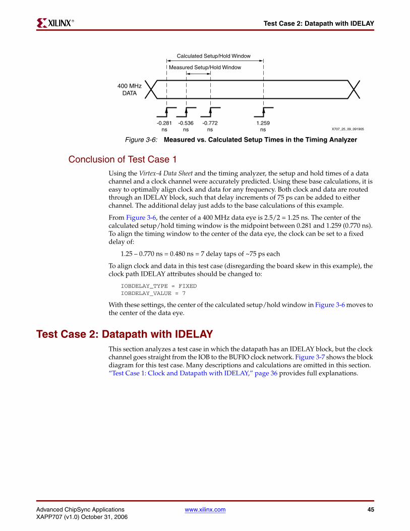
Advanced ChipSync Applications www.xilinx.com 45XAPP707 (v1.0) October 31, 2006
Test Case 2: Datapath with IDELAYR
Conclusion of Test Case 1Using the Virtex-4 Data Sheet and the timing analyzer, the setup and hold times of a data channel and a clock channel were accurately predicted. Using these base calculations, it is easy to optimally align clock and data for any frequency. Both clock and data are routed through an IDELAY block, such that delay increments of 75 ps can be added to either channel. The additional delay just adds to the base calculations of this example.
From Figure 3-6, the center of a 400 MHz data eye is 2.5/2 = 1.25 ns. The center of the calculated setup/hold timing window is the midpoint between 0.281 and 1.259 (0.770 ns). To align the timing window to the center of the data eye, the clock can be set to a fixed delay of:
1.25 – 0.770 ns = 0.480 ns = 7 delay taps of ~75 ps each
To align clock and data in this test case (disregarding the board skew in this example), the clock path IDELAY attributes should be changed to:
IOBDELAY_TYPE = FIXEDIOBDELAY_VALUE = 7
With these settings, the center of the calculated setup/hold window in Figure 3-6 moves to the center of the data eye.
Test Case 2: Datapath with IDELAYThis section analyzes a test case in which the datapath has an IDELAY block, but the clock channel goes straight from the IOB to the BUFIO clock network. Figure 3-7 shows the block diagram for this test case. Many descriptions and calculations are omitted in this section. “Test Case 1: Clock and Datapath with IDELAY,” page 36 provides full explanations.
Figure 3-6: Measured vs. Calculated Setup Times in the Timing Analyzer
400 MHzDATA
Calculated Setup/Hold Window
-0.281ns
-0.536ns
-0.772ns
1.259ns
Measured Setup/Hold Window
X707_25_09_091905

46 www.xilinx.com Advanced ChipSync ApplicationsXAPP707 (v1.0) October 31, 2006
Chapter 3: ISERDES TimingR
Theoretical Setup and Hold Calculations of Test Case 2From inspection of Figure 3-7, it is unclear if the data arrives before the clock because the clock path and datapath contain different types of blocks. To quantify the setup and hold times of this specific configuration, the individual delays in the datapath must be summed and compared to the sum of individual delays of the clock path. Table 3-8 and Table 3-9 show the descriptions of the individual delays.
Figure 3-7: ISERDES Datapath with IDELAY in Variable Mode (Initialized to Tap 0)
+
–
+
–
DATAPATH
CLOCKPATH
ISERDESFF’s
D
CLKBUFIO
IBUFDS
IBUFDS
TIOPI TNET TISDCK_D
TNET1 TNET2TIOPI
X707_26_10_100605
IDELAY
I O
Table 3-8: Datapath Timing Definitions
Timing Parameter Description
TIOPI Delay from the IOB pad through the LVDS input buffer to the I pin of the IOB pad
TNET Delay from the I pin of the IOB pad to the D input of the Data ISERDES/ILOGIC block
TISDCK_D Delay from the D input of the ISERDES block to the D flip-flops in the ISERDES block (setup and hold times of ISERDES)

Advanced ChipSync Applications www.xilinx.com 47XAPP707 (v1.0) October 31, 2006
Test Case 2: Datapath with IDELAYR
Each of the parameters in Table 3-8 and Table 3-9 has a best-case and worst-case value over PVT (as discussed in Overview of Setup and Hold Calculations). Net delays are generated by the timing analyzer and are not specified in the Virtex-4 Data Sheet because they are specific to this particular design configuration. TIOPI is specified in the Virtex-4 Data Sheet, but the timing analyzer adjusts the data sheet values to account for the effects of package skew in this specific design.
Table 3-10 and Table 3-11 show the values of the delays in the test case in Figure 3-7. The values are extracted directly from the timing report generated by the ISE Timing Analyzer (ISE 7.1 SP4) for a -10 speed grade device. Slowest and fastest paths are determined by summing the individual delay values. Setup and hold times are calculated from the slowest and fastest paths according to Equation 3-1 and Equation 3-2. See Appendix E, “ISERDES Timing Source Files,” for the actual timing report.
The final calculations are:
• Setup Time: SLOW DATA – FAST CLK = 2.368 – 1.963 = 0.405
• Hold Time: SLOW CLK – FAST DATA = 2.385 – 1.872 = 0.513
• Timing Window: 0.405 + 0.513 = 0.918 ns
The setup time and hold times are positive. Assuming that data and clock are phase-aligned (with some tolerance) at the input pins to the FPGA, this design does not meet timing over PVT for all -10 speed grade devices. Incrementing the delay chain in the
Table 3-9: Clock Path Timing Definitions
Timing Parameter Description
TIOPI Delay from the IOB pad through the LVDS input buffer to the I pin of the IOB pad
TNET1 Delay from the I pin of the IOB pad to the I input of BUFIO
TNET2 Delay from the BUFIO I input to the CLK input of the Data ISERDES block (the BUFIO delay is included in the overall net delay)
Table 3-10: Data Delay Calculation from ISE Timing Analyzer
Parameter Setup Time (SLOW DATA) Hold Time (FAST DATA)
TIOPI 1.350 ns 1.122 ns
TNET 0.117 ns 0.108 ns
TISDCK_D 0.901 ns -0.642 ns
TOTAL 2.368 ns 1.872 ns
Table 3-11: Clock Delay Calculation from ISE Timing Analyzer
Parameter Setup time (FAST CLK) Hold time (SLOW CLK)
TIOPI 1.074 ns 1.300 ns
TNET1 0.327 ns 0.355 ns
TNET2 0.562 ns 0.730 ns
TOTAL 1.963 ns 2.385 ns
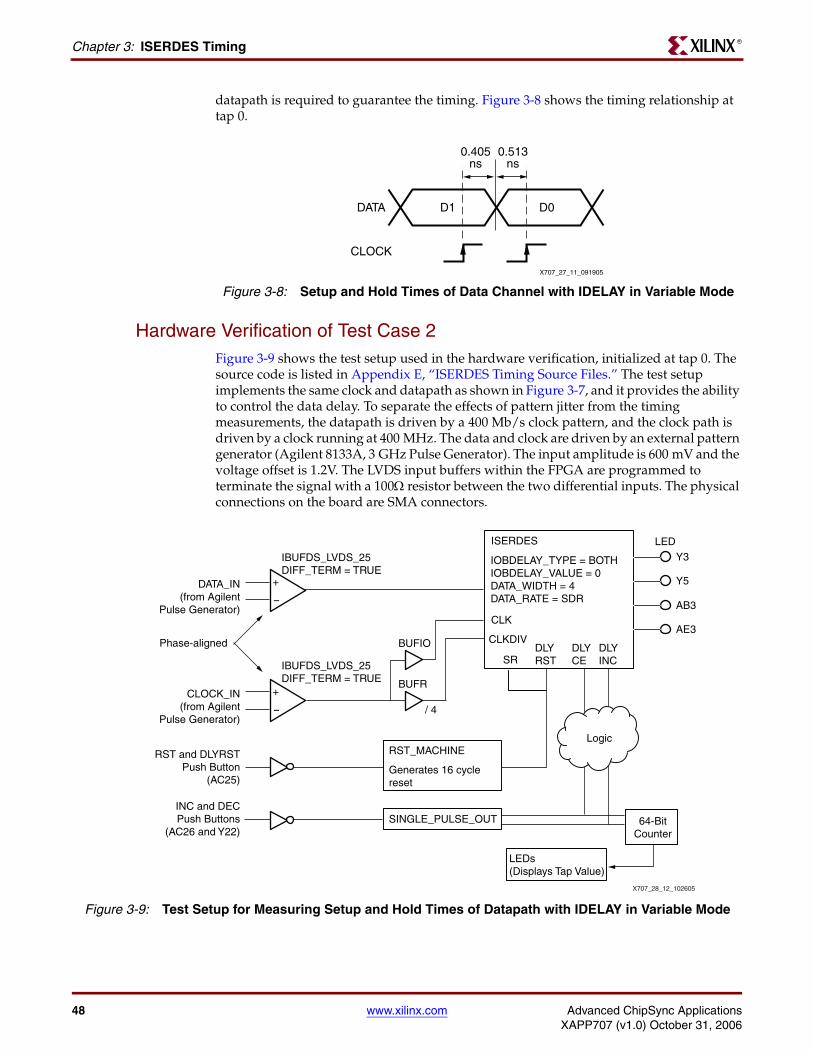
48 www.xilinx.com Advanced ChipSync ApplicationsXAPP707 (v1.0) October 31, 2006
Chapter 3: ISERDES TimingR
datapath is required to guarantee the timing. Figure 3-8 shows the timing relationship at tap 0.
Hardware Verification of Test Case 2Figure 3-9 shows the test setup used in the hardware verification, initialized at tap 0. The source code is listed in Appendix E, “ISERDES Timing Source Files.” The test setup implements the same clock and datapath as shown in Figure 3-7, and it provides the ability to control the data delay. To separate the effects of pattern jitter from the timing measurements, the datapath is driven by a 400 Mb/s clock pattern, and the clock path is driven by a clock running at 400 MHz. The data and clock are driven by an external pattern generator (Agilent 8133A, 3 GHz Pulse Generator). The input amplitude is 600 mV and the voltage offset is 1.2V. The LVDS input buffers within the FPGA are programmed to terminate the signal with a 100Ω resistor between the two differential inputs. The physical connections on the board are SMA connectors.
Figure 3-8: Setup and Hold Times of Data Channel with IDELAY in Variable Mode
D1DATA
CLOCK
0.513ns
D0
0.405ns
X707_27_11_091905
Figure 3-9: Test Setup for Measuring Setup and Hold Times of Datapath with IDELAY in Variable Mode
ISERDES
IOBDELAY_TYPE = BOTHIOBDELAY_VALUE = 0DATA_WIDTH = 4DATA_RATE = SDR
BUFR
/ 4
IBUFDS_LVDS_25DIFF_TERM = TRUE
IBUFDS_LVDS_25DIFF_TERM = TRUE
CLOCK_IN(from Agilent
Pulse Generator)
INC and DECPush Buttons
(AC26 and Y22)
RST and DLYRSTPush Button
(AC25)
LEDs(Displays Tap Value)
SINGLE_PULSE_OUT
RST_MACHINE
Generates 16 cyclereset
Phase-aligned
64-BitCounter
CLK
CLKDIVDLYRST
DLYCE
DLYINCSR
Logic
X707_28_12_102605
BUFIO
+
-
DATA_IN(from Agilent
Pulse Generator)
+
-
LEDY3
Y5
AB3
AE3
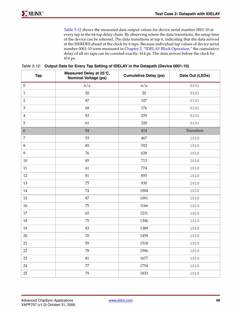
Advanced ChipSync Applications www.xilinx.com 49XAPP707 (v1.0) October 31, 2006
Test Case 2: Datapath with IDELAYR
Table 3-12 shows the measured data output values for device serial number 0001-10 at every tap in the 64-tap delay chain. By observing where the data transitions, the setup time of the device can be inferred. The data transitions at tap 6, indicating that the data arrived at the ISERDES ahead of the clock by 6 taps. Because individual tap values of device serial number 0001-10 were measured in Chapter 2, “IDELAY Block Operation,” the cumulative delay of all six taps can be counted exactly: 414 ps. The data arrives before the clock by 414 ps.
Table 3-12: Output Data for Every Tap Setting of IDELAY in the Datapath (Device 0001-10)
TapMeasured Delay at 25°C,
Nominal Voltage (ps)Cumulative Delay (ps) Data Out (LEDs)
0 n/a n/a 0101
1 20 20 0101
2 87 107 0101
3 69 176 0101
4 83 259 0101
5 61 320 0101
6 94 414 Transition
7 53 467 1010
8 85 552 1010
9 76 628 1010
10 85 713 1010
11 61 774 1010
12 81 855 1010
13 75 930 1010
14 74 1004 1010
15 87 1091 1010
16 75 1166 1010
17 65 1231 1010
18 75 1306 1010
19 83 1389 1010
20 70 1459 1010
21 59 1518 1010
22 78 1596 1010
23 81 1677 1010
24 77 1754 1010
25 79 1833 1010

50 www.xilinx.com Advanced ChipSync ApplicationsXAPP707 (v1.0) October 31, 2006
Chapter 3: ISERDES TimingR
26 75 1908 1010
27 69 1977 1010
28 79 2056 1010
29 84 2140 1010
30 68 2208 1010
31 80 2288 1010
32 68 2356 1010
33 94 2450 1010
34 54 2504 1010
35 74 2578 1010
36 59 2637 1010
37 90 2727 1010
38 70 2797 1010
39 78 2875 1010
40 67 2942 Transition
41 69 3011 0101
42 78 3089 0101
43 70 3159 0101
44 70 3229 0101
45 96 3325 0101
46 63 3388 0101
47 80 3468 0101
48 80 3548 0101
49 77 3625 0101
50 69 3694 0101
51 87 3781 0101
52 73 3854 0101
53 77 3931 0101
54 61 3992 0101
55 85 4077 0101
56 88 4165 0101
Table 3-12: Output Data for Every Tap Setting of IDELAY in the Datapath (Device 0001-10) (Continued)
TapMeasured Delay at 25°C,
Nominal Voltage (ps)Cumulative Delay (ps) Data Out (LEDs)

Advanced ChipSync Applications www.xilinx.com 51XAPP707 (v1.0) October 31, 2006
Test Case 2: Datapath with IDELAYR
There is some skew between the clock and data signals on the ML450 board that must be calibrated out of the measurements. This calibration is done by first calculating the delay of the clock and datapaths on the board and then calculating the difference. From the board skew calculations in Test Case 1, the clock path lags the datapath by 394 ps.
Accounting for board skew, the measured setup time of the data is given by Equation 3-4.
-414 ps – (-394 ps) = -0.020 ps Equation 3-4
The setup time measured for device 0001-10 under nominal conditions is -20 ps, which is almost no setup time at all. The clock samples the data almost perfectly on the transition, such that over PVT the timing is likely to fail. The same calculations were performed on the same device under a variety of extreme conditions, as well as another device (6022-12). Table 3-13 and Table 3-14 show the setup times measured for both of these devices under various conditions. There is very little variation in the timing measurements in this test case, but the timing of device 0001-10 fails at -40°C with VCCINT margined to -5%.
57 73 4238 0101
58 78 4316 0101
59 82 4398 0101
60 86 4484 0101
61 63 4547 0101
62 69 4616 0101
63 109 4725 0101
Table 3-12: Output Data for Every Tap Setting of IDELAY in the Datapath (Device 0001-10) (Continued)
TapMeasured Delay at 25°C,
Nominal Voltage (ps)Cumulative Delay (ps) Data Out (LEDs)
Table 3-13: Measured Setup Times of Device 0001-10 under Various Conditions
Temperature (°C) VCCINT Supply Measured Setup Time (ps)
+25 Nominal -20
+25 -5% -20
+25 +5% -20
+85 Nominal -20
+85 -5% -20
+85 +5% -20
-40 Nominal -20
-40 -5% 74
-40 +5% -20

52 www.xilinx.com Advanced ChipSync ApplicationsXAPP707 (v1.0) October 31, 2006
Chapter 3: ISERDES TimingR
The range of measured setup values falls comfortably within the setup and hold calculations generated by the ISE Timing Analyzer for a -10 device. Devices of all speed grades are required to meet -10 speed grade timing. Figure 3-10 shows the timing analyzer setup time calculations and the measured setup times for devices 0001-10 and 6022-12. The timing analyzer predicted that the design was not guaranteed to meet timing, and the hardware results did not meet timing.
Conclusion of Test Case 2Using the Virtex-4 Data Sheet and the ISE Timing Analyzer, the setup and hold times of a data channel and a clock channel were accurately predicted. Using these base calculations, it is easy to optimally align clock and data for any frequency. The data is routed through an IDELAY block, such that delay increments of 75 ps can be added to the datapath. The additional delay just adds to the base calculations of this example.
From Figure 3-10, the center of a 400 MHz data eye is 2.5/2 = 1.25 ns. The center of the calculated setup/hold timing window is the midpoint between –0.405 and 0.513 (0.054 ns). To align the timing window to the center of the data eye, the data can be set to a fixed delay of:
1.25 + 0.054 ns = 1.304 ns = 17 delay taps of ~75 ps each
Table 3-14: Measured Setup Times of Device 6022-12 under Various Conditions
Temperature (°C) VCCINT Supply Measured Setup Time (ps)
+25 Nominal -19
+25 -5% -19
+25 +5% -19
+85 Nominal -19
+85 -5% -19
+85 +5% -19
-40 Nominal -19
-40 -5% -19
-40 +5% -19
Figure 3-10: Measured Setup Times for Devices 0001-10 and 6022-12 vs. Setup Times Calculated in the ISE Timing Analyzer
400 MHzDATA
Measured Setup/Hold Window
Calculated Setup/Hold Window
-0.020ns
0.074ns
0.513ns
0.405ns
X707_29_13_100605

Advanced ChipSync Applications www.xilinx.com 53XAPP707 (v1.0) October 31, 2006
Test Case 3: Data and Clock Path with no IDELAYR
To align clock and data in this test case (disregarding the board skew in this example), the data path IDELAY attributes must be changed to:
IOBDELAY_TYPE = FIXEDIOBDELAY_VALUE = 17
With these settings, the data eye in Figure 3-10 is shifted to the right, aligning the center of the calculated setup/hold window to the center of the data eye.
Test Case 3: Data and Clock Path with no IDELAYThe purpose of this section is to explain and derive as accurately as possible the data sheet parameter TPSCS and account for any inaccuracies. There is no hardware verification for this section because there is no way to delay clock or data to examine the timing.
This section analyzes a test case that is specified in the Virtex-4 Data Sheet. In the data sheet section called “ChipSync Source Synchronous Switching Characteristics,” the timing parameter called TPSCS is defined as the pin-to-pin setup and hold time of a ChipSync data input. This number is more complex than other timing parameters in the data sheet because it is calculated from the setup and hold times of individual elements in the datapath. The ISE Timing Analyzer calculates TPSCS using a test case very similar to the test case described in this section. In this test case, the data channel goes directly from the IOB to the ISERDES registers, and the clock channel goes directly from the IOB to the BUFIO clock network. Figure 3-11 shows the block diagram for this test case.
Theoretical Setup and Hold Calculations of Test Case 3From inspection of Figure 3-11, the clock path is longer than the datapath, because there is an extra element (BUFIO) in the clock path. Therefore, the data is expected to arrive before the clock. To quantify the setup and hold times of this specific configuration, the individual delays in the datapath must be summed and compared to the sum of individual delays of the clock path. Table 3-15 and Table 3-16 show the descriptions of the individual delays.
Figure 3-11: Measuring Setup and Hold Times of Data and Clock Paths with No IDELAY
+
–
+
–
DATAPATH
CLOCKPATH
ISERDESFFs
D
CLKBUFIO
IBUFDS
IBUFDS
TIOPI TNET TISDCK_D_NONE
TNET1 TNET2TIOPI
X707_30_14_102605

54 www.xilinx.com Advanced ChipSync ApplicationsXAPP707 (v1.0) October 31, 2006
Chapter 3: ISERDES TimingR
Each of the parameters in Table 3-15 and Table 3-16 has a best-case value and a worst-case value over PVT (as discussed in Overview of Setup and Hold Calculations). Net delays are generated by the timing analyzer and not specified in the Virtex-4 Data Sheet, because they are specific to this particular design configuration. TIOPI is specified in the Virtex-4 Data Sheet, but the timing analyzer adjusts the data sheet values to account for the effects of package skew in this specific design.
Table 3-17 and Table 3-18 show the values of the delays in the test case in Figure 3-11. The values are extracted directly from the timing report generated by the ISE Timing Analyzer (ISE 7.1 SP4) for a -10 speed grade device. Slowest and fastest paths are determined by summing the individual delay values together. Setup and hold times are calculated from the slowest and fastest paths according to Equation 3-1 and Equation 3-2.
Table 3-15: Datapath Timing Definitions
Timing Parameter Description
TIOPI Delay from the IOB pad through the LVDS input buffer to the I pin of the IOB pad
TNET Delay from the I pin of the IOB pad to the D input of the Data ISERDES/ILOGIC block
TISDCK_D_NONE Delay from the D input of the ISERDES to the D flip-flops in the ISERDES (setup and hold times of ISERDES)
Table 3-16: Clock Path Timing Definitions
Timing Parameter Description
TIOPI Delay from the IOB pad through the LVDS input buffer to the I pin of the IOB pad
TNET1 Delay from the I pin of the IOB pad to the I input of BUFIO
TNET2 Delay from the BUFIO I input to the CLK input of the Data ISERDES (BUFIO delay is included in the overall net delay)
Table 3-17: Data Delay Calculation from ISE Timing Analyzer
Parameter Setup Time (SLOW DATA) Hold Time (FAST DATA)
TIOPI 1.350 ns 1.122 ns
TNET 0.117 ns 0.108 ns
TISDCK_D 0.156 ns 0.043 ns
TOTAL 1.623 ns 1.187 ns
Table 3-18: Clock Delay Calculation from ISE Timing Analyzer
Parameter Setup Time (FAST CLK) Hold Time (SLOW CLK)
TIOPI 1.074 ns 1.300 ns
TNET1 0.327 ns 0.355 ns
TNET2 0.562 ns 0.730 ns
TOTAL 1.963 ns 2.385 ns

Advanced ChipSync Applications www.xilinx.com 55XAPP707 (v1.0) October 31, 2006
Clock-Data Alignment SchemesR
The final calculations are:
Setup Time: SLOW DATA – FAST CLK = 1.623 – 1.963 = -0.340
Hold Time: SLOW CLK – FAST DATA = 2.385 – 1.187 = 1.198
Timing Window: 1.198 – 0.340 = 0.858 ns
The setup time is negative, and the hold time is positive. Assuming that data and clock are phase-aligned (with some tolerance) at the input pins to the FPGA, this design meets timing across PVT for all -10 speed grade devices. Figure 3-12 shows the timing relationship with IDELAY in Variable mode, initialized to tap 0.
From Table 3-19, the calculation of TPSCS in Test Case 3 is very accurate, differing from the Virtex-4 Data Sheet by only 100 ps. The calculation of TPHCS differs from the data sheet by only 28 ps. The slight differences are due to the fact that package skew is not included in the data sheet calculations. The timing analyzer factored package skew into the calculations of Test Case 3.
The source code of Test Case 3 is identical to Test Case 2, except that the data ISERDES attribute “IOBDELAY_TYPE” was changed to NONE. See Appendix E, “ISERDES Timing Source Files,” for the source files of Test Case 2.
Clock-Data Alignment SchemesThere are many ways to use ChipSync technology to align a clock with one or more data channels. The objective of all alignment schemes is to position the sampling point (clock’s rising or falling edge) as closely as possible to the center of the data valid window. The accuracy of the alignment scheme determines the maximum performance of a source synchronous interface.
Static alignment is a scheme that has no ability to dynamically adjust the delay of the clock or data channel. Test Cases 1 through 3 are examples of static alignment schemes. The clock and data must be set to fixed delays that are guaranteed to meet timing for all specified devices, temperatures, and voltages. The fixed delays must also account for timing inaccuracies due to package skew, duty-cycle distortion (for DDR), and clock network skew. All of these variations cause very large setup and hold timing windows like those of Test Cases 1 through 3, repeated in Table 3-20.
Figure 3-12: Setup and Hold Times of Clock and Data Channels
Table 3-19: Comparison of Data Sheet to Calculations of Test Case 3
Parameter Virtex-4 Data Sheet (ns) Test Case 3 Calculations (ns)
TPSCS -0.440 -0.340
TPHCS 1.170 1.198
D1DATA
CLOCK
1.198 ns
-0.340 ns
D0
X707_31_15_091905

56 www.xilinx.com Advanced ChipSync ApplicationsXAPP707 (v1.0) October 31, 2006
Chapter 3: ISERDES TimingR
Every source of variation in a design causes the static timing window to expand. In Table 3-20, the test cases with IDELAY in the datapath have larger timing windows than the case without IDELAY.
The measured results of Test Cases 1 and 2 were much smaller timing windows than the timing analyzer calculations. No individual part spans the entire timing window predicted by the timing analyzer. However, the small timing window of a large number of devices eventually fills in the large timing window predicted by the timing analyzer, as illustrated in Figure 3-13. Figure 3-13 shows that TPSCS and TPHCS determine the minimum data valid window required for a static alignment scheme. When a static alignment design goes into production, it must meet timing for all parts under all conditions. Therefore, a static scheme requires a data eye width of at least 900 ps to 1000 ps. A data width requirement of this size severely limits the performance capability of a static design. Generally, static implementations should not run above 600 Mb/s.
Figure 3-14 shows measured eye widths of an actual 622 Mb/s data eye in a 16-channel SFI-4 receiver design running in a Virtex-4 device. The data is transmitted from a Virtex-4 transmitter on an ML450 board and looped back to the receiver through a 12-inch ribbon cable and ~10 inches of trace. This represents a significant load on the transmitted signal The eye width is almost too small for a static alignment scheme. Considering the size of the PRBS15 data eye, a static alignment scheme is barely adequate and is not recommended.
Table 3-20: Test Case Timing Window Spreads
Static Alignment Case Design DescriptionTiming Window Spread
(ns)
Test Case 1 Data and clock with IDELAY 0.978
Test Case 2 Data with IDELAY 0.918
Test Case 3 No IDELAY 0.858
Figure 3-13: Data Windows in a Static Alignment Scheme
Setup/Hold Window
Devices
DATA
A
BC
D
TPSCS
TSAMP
TPHCS X707_32_16_092005
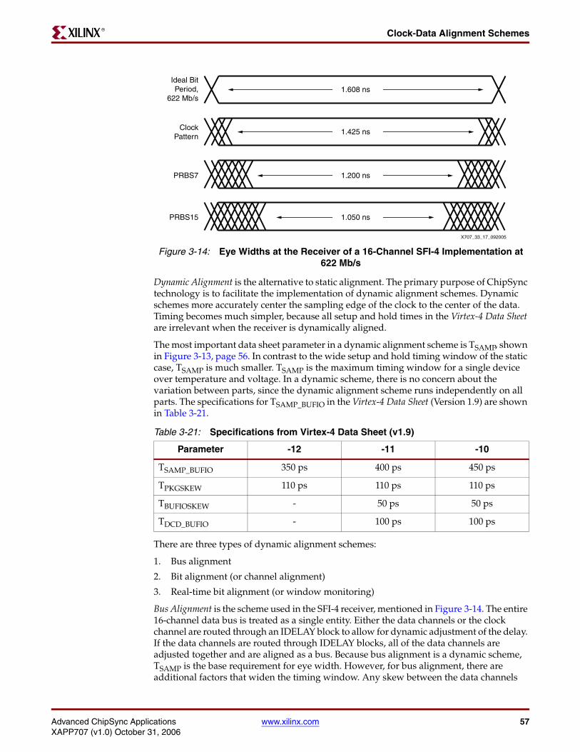
Advanced ChipSync Applications www.xilinx.com 57XAPP707 (v1.0) October 31, 2006
Clock-Data Alignment SchemesR
Dynamic Alignment is the alternative to static alignment. The primary purpose of ChipSync technology is to facilitate the implementation of dynamic alignment schemes. Dynamic schemes more accurately center the sampling edge of the clock to the center of the data. Timing becomes much simpler, because all setup and hold times in the Virtex-4 Data Sheet are irrelevant when the receiver is dynamically aligned.
The most important data sheet parameter in a dynamic alignment scheme is TSAMP, shown in Figure 3-13, page 56. In contrast to the wide setup and hold timing window of the static case, TSAMP is much smaller. TSAMP is the maximum timing window for a single device over temperature and voltage. In a dynamic scheme, there is no concern about the variation between parts, since the dynamic alignment scheme runs independently on all parts. The specifications for TSAMP_BUFIO in the Virtex-4 Data Sheet (Version 1.9) are shown in Table 3-21.
There are three types of dynamic alignment schemes:
1. Bus alignment
2. Bit alignment (or channel alignment)
3. Real-time bit alignment (or window monitoring)
Bus Alignment is the scheme used in the SFI-4 receiver, mentioned in Figure 3-14. The entire 16-channel data bus is treated as a single entity. Either the data channels or the clock channel are routed through an IDELAY block to allow for dynamic adjustment of the delay. If the data channels are routed through IDELAY blocks, all of the data channels are adjusted together and are aligned as a bus. Because bus alignment is a dynamic scheme, TSAMP is the base requirement for eye width. However, for bus alignment, there are additional factors that widen the timing window. Any skew between the data channels
Figure 3-14: Eye Widths at the Receiver of a 16-Channel SFI-4 Implementation at 622 Mb/s
Table 3-21: Specifications from Virtex-4 Data Sheet (v1.9)
Parameter -12 -11 -10
TSAMP_BUFIO 350 ps 400 ps 450 ps
TPKGSKEW 110 ps 110 ps 110 ps
TBUFIOSKEW - 50 ps 50 ps
TDCD_BUFIO - 100 ps 100 ps
Ideal BitPeriod,
622 Mb/s
ClockPattern
PRBS7
PRBS15
X707_33_17_092005
1.608 ns
1.425 ns
1.200 ns
1.050 ns

58 www.xilinx.com Advanced ChipSync ApplicationsXAPP707 (v1.0) October 31, 2006
Chapter 3: ISERDES TimingR
causes the “collective data eye” of all 16 channels to appear smaller. Thus, package skew and clock network skew must be added to TSAMP according to Equation 3-5. If the interface is DDR, duty-cycle distortion must also be added to the timing window.
Timing Window = TSAMP_BUFIO + TPKGSKEW + TBUFIOSKEW Equation 3-5
= 450 + 110 + 50 = 610 ps
The minimum data eye width for a bus alignment scheme is 610 ps. It is recommended that bus alignment implementations not run above 700 Mb/s. Figure 3-15 shows measured eye widths of an actual 700 Mb/s data eye in a 16-channel SFI-4 receiver design running in a Virtex-4 device. The eye diagram already includes the effects of package skew and clock skew, and the timing window is wider than TSAMP_BUFIO (with margin).
Bit alignment is similar to bus alignment, except that each data channel is aligned independently. This scheme eliminates any error due to package skew and clock network skew. If the interface is DDR, duty-cycle distortion must also be added to the timing window, as shown in Equation 3-6.
Timing Window = TSAMP_BUFIO + TDCD_BUFIO = 450 + 100 = 550 ps Equation 3-6
The minimum data eye width for a bit alignment scheme is 550 ps. It is recommended that bit alignment implementations not run above 900 Mb/s. Figure 3-16 shows measured eye widths of an actual 1000 Mb/s data eye in a 16-channel DDR receiver design running in a Virtex-4 device. The eye diagram already includes the effect of duty cycle distortion, but the timing window still is not wider than TSAMP_BUFIO. To meet timing above 900 Mb/s, another alignment scheme is needed.
Figure 3-15: Eye Widths at the Receiver of a 16-Channel SFI-4 Implementation at 700 Mb/s
Ideal BitPeriod,
700 Mb/s
ClockPattern
PRBS7
PRBS15
X707_34_18_092005
1.429 ns
1.275 ns
0.825 ns
0.750 ns

Advanced ChipSync Applications www.xilinx.com 59XAPP707 (v1.0) October 31, 2006
Clock-Data Alignment SchemesR
Real-Time Bit Alignment is a version of bit alignment that continues to align the data channels while the link is running. At every I/O site, there is a master ISERDES and a slave ISERDES. In a real-time alignment scheme, the master ISERDES handles the data while the slave ISERDES interrogates the data eye to continually make sure that the sampling point is at the center of the eye. Theoretically, a link could run with an eye width of two delay taps, or 150 ps, because it would guarantee three error-free points in the data eye. Real-time monitoring eliminates all consideration of PVT variation. It is also the most complex implementation and is not recommended unless absolutely necessary.
Higher levels of performance require more accurate clock and data-alignment schemes. A summary of the recommendations in this section are shown in Table 3-22.
Figure 3-16: Eye Widths at the Receiver of a 16-Channel DDR Implementation at 1000 Mb/s
Ideal BitPeriod,1 Gb/s
ClockPattern
PRBS7
PRBS15
X707_35_19_092005
1.000 ns
0.825 ns
0.450 ns
0.375 ns
Table 3-22: Alignment Scheme Recommendations
Alignment Scheme Minimum Data Eye Width Recommendation
Static (Setup and Hold Timing) TPHCS - |TPSCS| + TPKGSKEW + TDCD_BUFIO(1) ≤ 600 Mb/s
Bus Alignment TSAMP_BUFIO + TPKGSKEW + TBUFIOSKEW + TDCD_BUFIO(1) ≤ 700 Mb/s
Bit Alignment TSAMP_BUFIO + TDCD_BUFIO(1) ≤ 900 Mb/s
Real-Time Bit Alignment 2 delay taps + TDCD_BUFIO(1) ± estimated tap inaccuracy(2) ≤ 1000 Mb/s
Notes: 1. Duty-cycle distortion is only included for DDR designs.2. See “Tap Delay Values” in Chapter 2.

60 www.xilinx.com Advanced ChipSync ApplicationsXAPP707 (v1.0) October 31, 2006
Chapter 3: ISERDES TimingR
Advanced ChipSync Applications www.xilinx.com 61XAPP707 (v1.0) October 31, 2006
R
Chapter 4
Clocking and Performance
This chapter contains the following sections:
• “Overview of Clock Regions and I/O”
• “Interfacing BUFR to BUFG”
• “Clock and I/O Performance”
• “Multiple Interfaces”
The I/O and regional clock networks are a new feature in Virtex-4 devices, and they play a fundamental role in ChipSync operation. They behave differently than global clock networks. More restrictions are placed on I/O and regional networks to achieve better performance than global clocks and DCMs can achieve. In this chapter, these restrictions and performance advantages are described in the context of common applications. Also, the interaction between global and regional networks is addressed.
Overview of Clock Regions and I/OI/O clocks and regional clock nets do not propagate throughout an entire device. Instead, I/O and regional clock distribution is defined in terms of clock regions. The size of a clock region is the same for all device types, and the contents of a clock region are shown in Table 4-1. There are 16 differential I/O in every clock region, but only 14 of them can be used as LVDS transmitters. The remaining two differential I/Os are “low capacity” and do not have LVDS transmitters (as a way of lowering input capacitance).
Table 4-1: Contents of a Single Clock Region
Resources Quantity in Each Clock Region
Single-Ended I/O 32
Differential I/O Total 16
Full Capacity 14
Low Capacity
(Clock Capable)
2
I/O Clock Buffer (BUFIO) 2
Regional Clock Buffer (BUFR) 2

62 www.xilinx.com Advanced ChipSync ApplicationsXAPP707 (v1.0) October 31, 2006
Chapter 4: Clocking and PerformanceR
Every I/O and regional clock buffer in a Virtex-4 device can drive the clock region in which it is located, as well as the two adjacent clock regions. There is no way for an I/O or regional network to be internally connected to other I/O or regional clock networks. The span of the ChipSync networks is limited to three clock regions.
Interfacing BUFR to BUFGIf ChipSync technology is used, the logic at the backend of an interface design in a regional clock domain must communicate with the rest of the system on a global clock domain. There must be a method for information to cross the regional and global domains. It is strongly recommended that a FIFO be used for this transfer. In Virtex-4 FPGAs, dedicated FIFO control logic is built into the block RAM that facilitates the implementation of FIFOs. The FIFO16 primitive is described in detail in UG070, Virtex-4 User Guide, and all source synchronous reference designs for the ML450 Networking Interfaces board use the FIFO16 primitive to bridge between the regional and global clock domains.
Physically connecting a regional clock domain to a global clock domain is not recommended, because it requires the clock to use local routing to get from one domain to the other. There is no dedicated switch between a global and regional clock network. They are independent of one another. Locally routing a clock causes unpredictable effects on signal integrity and timing. BUFIO and BUFR are guaranteed to be in phase at the inputs of the ISERDES to sample incoming data correctly. If the regional clock is routed to a global clock, the timing relationship with BUFIO is no longer guaranteed (see Figure 4-1).

Advanced ChipSync Applications www.xilinx.com 63XAPP707 (v1.0) October 31, 2006
Interfacing BUFR to BUFGR
Under certain circumstances, the place-and-route software allows the physical connection of BUFR and BUFG. There are three columns of I/O in Virtex-4 devices: left, right, and center columns. All global clocks are in the center column. Because the center column is on the left side of the device, only regional clocks on the left side of the device route to global clocks in the center column, as shown in Figure 4-2.
To illustrate both cases, there are two test designs. The first design attempts to route a BUFR from the left side of the device to a BUFG. The ISE tools run without errors and generate a design like the one in Figure 4-3.
Figure 4-1: CLK and CLKDIV Connections
BUFIO
ISERDES
CLK
CLKDIV
BUFR
(a) CLK and CLKDIV are skew-matched at the ISERDES inputs by design.
(b) The CLK and CLKDIV phase relationship is unknown at the ISERDES inputs.
BUFIO
ISERDES
CLK
CLKDIV
BUFR BUFR
X707_45_01_092005
Local Routing

64 www.xilinx.com Advanced ChipSync ApplicationsXAPP707 (v1.0) October 31, 2006
Chapter 4: Clocking and PerformanceR
The second design attempts to route a BUFR from the right side of the device to a global network. The ISE tools produce this error during the place-and-route portion of the second implementation:
WARNING: Place:659 - Regional Clock Net “clkin_bufr” cannot possibly be routed to component “GLOBAL_CLK” (placed in clock region 6), since it is too far away from source BUFR “RX_CLK_BUFR” (placed in clock region 7). The situation may be caused by user constraints, or the complexity of the design. Constraining the components related to the regional clock properly may guide the tool to find a solution.
The design is unroutable in the ISE tools and requires a more complex local routing scheme to connect the regional and global clocks.
Figure 4-2: Center Column of Logic Resources (including Global Clocks) on the Left Side of the Device
UG070_1_17_071304
All clock regionsspan half the die
All clock regions are 16 CLBs tall(8 CLBs up and 8 CLBs down)
XC4VLX15 has 8 Clock Regions XC4VLX100 has 24 Clock Regions
Center ColumnLogic Resources
8 CLBs
8 CLBs
8 CLBs
8 CLBs
Figure 4-3: Automatic Routing of BUFR to BUFG in ISE Tools (Not Recommended)
Clock Input(left I/O column)
IOB SwitchBox
BUFIO BUFR BUFG
Local Routing
X707_46_02_092005

Advanced ChipSync Applications www.xilinx.com 65XAPP707 (v1.0) October 31, 2006
Clock and I/O PerformanceR
Clock and I/O PerformanceThe two different types of clocking schemes that can be used to clock ISERDES and OSERDES are shown in Figure 4-4. The first scheme uses I/O and regional clocks, and the second scheme uses global clocks with a DCM or PMCD. The scheme in Figure 4-4(b) is an easier implementation than Figure 4-4(a) because there are fewer restrictions on global clocks than regional clocks. The task of interfacing multiple clock domains as discussed in “Interfacing BUFR to BUFG” is not a consideration in Figure 4-4(b). However, the performance of Figure 4-4(a) is much better than Figure 4-4(b) because I/O clock networks have higher performance than global clock networks.
The limitations of the scheme in Figure 4-4(b) are determined by the DCM and PMCD limitations, while the limitations of the scheme in Figure 4-4(a) are determined by the BUFIO limitations. Those limitations are shown in Table 4-2. The Virtex-4 Data Sheet contains the most up-to-date values.
Figure 4-4: Clocking Schemes
X707_47_03_092005
ISERDES
CLKDIV
BUFRBUFIOClockInput
(a) Clocking Scheme using I/O and Regional Networks
(b) Clocking Scheme using Global Networks with a DCM or PMCD
CLK
ISERDESDCM or PMCD
CLKDIV
BUFGBUFGClockInput
CLKBUFG
Table 4-2: Specifications from Virtex-4 Data Sheet (V1.11)
Timing Parameter -12 -11 -10
PMCD CLKIN_FREQ_PMCD_CLKA_MAX 500 MHz 450 MHz 400 MHz
DCM CLKOUT_FREQ_1X_HF_MS_MAX 500 MHz 450 MHz 400 MHz
BUFIO T_BUFIO_MAX_FREQ 710 MHz 710 MHz 644 MHz

66 www.xilinx.com Advanced ChipSync ApplicationsXAPP707 (v1.0) October 31, 2006
Chapter 4: Clocking and PerformanceR
Single data rate interfaces above 500 Mb/s must use BUFIO to distribute the clock in the transmitter and receiver because the global buffer resources are limited to 500 MHz in the fastest speed grade. Clock performance is especially important in SDR applications because it is normally the limiting factor in the overall performance of SDR designs. In a 700 Mb/s SDR application, the clock must be forwarded to the receiver at 700 MHz, which pushes the clock network to its performance margin. In a 700 Mb/s DDR application, the clock is forwarded to the receiver at only 350 MHz, which is well within the abilities of the clock networks. For DDR applications, the limitation of overall performance is the I/O speed. Although a 1 Gb/s application requires only a 500 MHz clock, it requires the I/O to operate at the high end of the performance margin. In spite of the reduced importance of clocking in DDR applications, it is still recommended that DDR interfaces above 800 Mb/s use BUFIO because it provides more performance margin in any given speed grade. There is less clock skew and duty cycle distortion on BUFIO than on BUFG.
Multiple InterfacesDesigns often consist of multiple interfaces of SFI-4 or SPI-4.2. On a global domain, multiple interfaces are simple to implement, but given the restrictions of BUFIO and BUFR, multiple interfaces can be more of a challenge. 16-channel LVDS interfaces are very common, so this section examines the challenge of implementing multiple 16-channel differential interfaces.
Because BUFIO and BUFR only span three clock regions, the number of interfaces that can run on that network is limited. From Table 4-1, there are 16 differential I/O in a clock region, which means that there are 48 differential I/O in three clock regions.
16-channel Source Synchronous TX requirements:
• 16 differential I/O for data
• 1 differential I/O for the forwarded clock
• 1 differential I/O for the clock input (i.e., from board oscillator)
16-channel Source Synchronous RX requirements:
• 16 differential I/O for data
• 1 differential I/O for the received forwarded clock
Table 4-3 shows that only two 16-channel interfaces can be implemented in three clock regions. The transmitter fits within three regions, and the receiver fits within three regions. If there are two transmitters in three regions, then they share the same clock input and use a single forwarded clock output. In the dual receiver, there is a received clock along with the 16 data channels. The dual interface scenario is very simple.
Table 4-3: Interface Requirements vs. LVDS I/O in BUFIO Network
Number of Interfaces
(16 Channel)Required I/Os (RX)
Available RX I/Os in Three Regions
Required I/Os (TX)Available TX I/Os in
Three Regions
1 17 48 18 42
2 33 48 34 42
3 49 48 50 42
4 65 48 66 42

Advanced ChipSync Applications www.xilinx.com 67XAPP707 (v1.0) October 31, 2006
Multiple InterfacesR
Three and four interfaces are more complex to implement. Two BUFIO/BUFR networks must be used for the transmitter, and two more must be used for the receiver. The biggest challenge is getting the high-frequency board oscillator output onto both BUFIO transmitter networks. Because there are no internal connections between BUFIO networks within the FPGA, the clock must be divided on the board and driven into two separate inputs of the FPGA. Figure 4-5 shows a block diagram of four interfaces in a single device.
Figure 4-5: Four 16-Channel LVDS Interfaces Implemented Using Multiple BUFIO/BUFR Clock Networks
Clock Region
Clock Region
BUFIO
Clock Region
Clock Region
Clock Region
BUFIO
Clock Region
Clock Region
32 LVDS Data
X707_48_04_092005
32 LVDS Data
BoardOscillator
1 LVDS Clock
1 LVDS Clock
4 Receivers in Virtex-4 FPGA4 Transmitters in Virtex-4 FPGA
Clock Region
BUFIO
Clock Region
Clock Region
Clock Region
BUFIO
Clock Region
LVDSSplitter

68 www.xilinx.com Advanced ChipSync ApplicationsXAPP707 (v1.0) October 31, 2006
Chapter 4: Clocking and PerformanceR
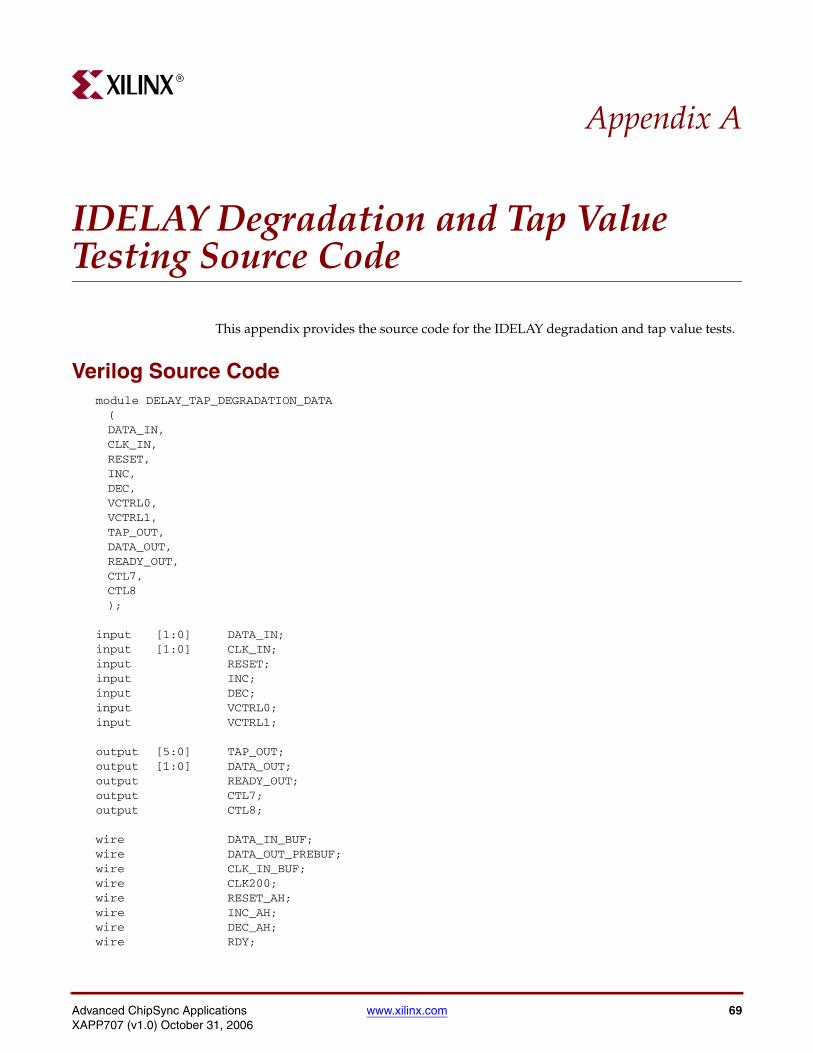
Advanced ChipSync Applications www.xilinx.com 69XAPP707 (v1.0) October 31, 2006
R
Appendix A
IDELAY Degradation and Tap Value Testing Source Code
This appendix provides the source code for the IDELAY degradation and tap value tests.
Verilog Source Codemodule DELAY_TAP_DEGRADATION_DATA (DATA_IN,CLK_IN,RESET,INC,DEC,VCTRL0,VCTRL1,TAP_OUT,DATA_OUT,READY_OUT,CTL7,CTL8);
input [1:0] DATA_IN;input [1:0] CLK_IN;input RESET;input INC;input DEC;input VCTRL0;input VCTRL1;
output [5:0] TAP_OUT;output [1:0] DATA_OUT;output READY_OUT;output CTL7;output CTL8;
wire DATA_IN_BUF;wire DATA_OUT_PREBUF;wire CLK_IN_BUF;wire CLK200;wire RESET_AH;wire INC_AH;wire DEC_AH;wire RDY;
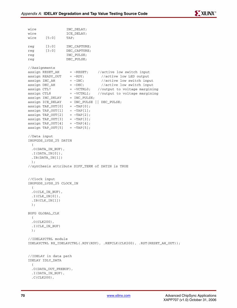
70 www.xilinx.com Advanced ChipSync ApplicationsXAPP707 (v1.0) October 31, 2006
Appendix A: IDELAY Degradation and Tap Value Testing Source CodeR
wire INC_DELAY;wire ICE_DELAY;wire [5:0] TAP;
reg [3:0] INC_CAPTURE;reg [3:0] DEC_CAPTURE;reg INC_PULSE;reg DEC_PULSE;
//Assignmentsassign RESET_AH = ~RESET; //active low switch inputassign READY_OUT = ~RDY; //active low LED outputassign INC_AH = ~INC; //active low switch inputassign DEC_AH = ~DEC; //active low switch inputassign CTL7 = ~VCTRL0; //output to voltage margining assign CTL8 = ~VCTRL1; //output to voltage marginingassign INC_DELAY = INC_PULSE;assign ICE_DELAY = INC_PULSE || DEC_PULSE;assign TAP_OUT[0] = ~TAP[0];assign TAP_OUT[1] = ~TAP[1];assign TAP_OUT[2] = ~TAP[2];assign TAP_OUT[3] = ~TAP[3];assign TAP_OUT[4] = ~TAP[4];assign TAP_OUT[5] = ~TAP[5];
//Data inputIBUFGDS_LVDS_25 DATIN(.O(DATA_IN_BUF), .I(DATA_IN[0]), .IB(DATA_IN[1]));
//synthesis attribute DIFF_TERM of DATIN is TRUE
//Clock inputIBUFGDS_LVDS_25 CLOCK_IN(.O(CLK_IN_BUF), .I(CLK_IN[0]), .IB(CLK_IN[1]));
BUFG GLOBAL_CLK (.O(CLK200), .I(CLK_IN_BUF));
//IDELAYCTRL moduleIDELAYCTRL RX_IDELAYCTRL(.RDY(RDY), .REFCLK(CLK200), .RST(RESET_AH_OUT));
//IDELAY in data pathIDELAY IDLY_DATA(.O(DATA_OUT_PREBUF),.I(DATA_IN_BUF),.C(CLK200),
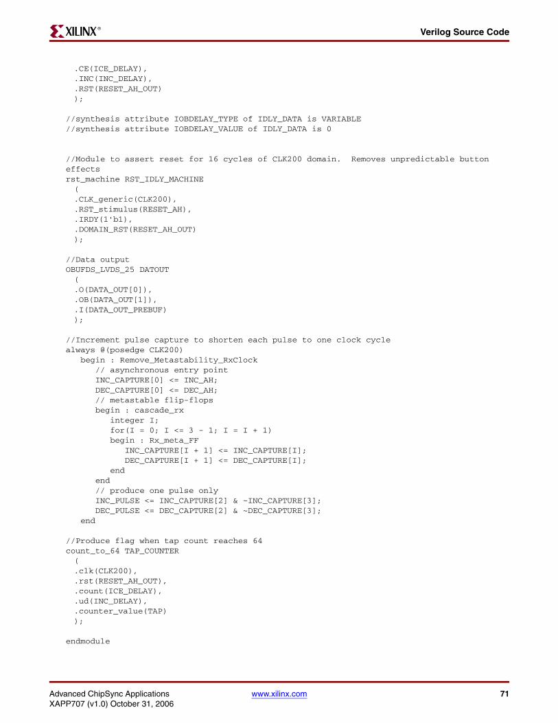
Advanced ChipSync Applications www.xilinx.com 71XAPP707 (v1.0) October 31, 2006
Verilog Source CodeR
.CE(ICE_DELAY),
.INC(INC_DELAY),
.RST(RESET_AH_OUT));
//synthesis attribute IOBDELAY_TYPE of IDLY_DATA is VARIABLE//synthesis attribute IOBDELAY_VALUE of IDLY_DATA is 0
//Module to assert reset for 16 cycles of CLK200 domain. Removes unpredictable button effectsrst_machine RST_IDLY_MACHINE(.CLK_generic(CLK200),.RST_stimulus(RESET_AH),.IRDY(1'b1),.DOMAIN_RST(RESET_AH_OUT));
//Data outputOBUFDS_LVDS_25 DATOUT(.O(DATA_OUT[0]), .OB(DATA_OUT[1]), .I(DATA_OUT_PREBUF));
//Increment pulse capture to shorten each pulse to one clock cyclealways @(posedge CLK200) begin : Remove_Metastability_RxClock // asynchronous entry point INC_CAPTURE[0] <= INC_AH; DEC_CAPTURE[0] <= DEC_AH; // metastable flip-flops begin : cascade_rx integer I; for(I = 0; I <= 3 - 1; I = I + 1) begin : Rx_meta_FF INC_CAPTURE[I + 1] <= INC_CAPTURE[I]; DEC_CAPTURE[I + 1] <= DEC_CAPTURE[I]; end end // produce one pulse only INC_PULSE <= INC_CAPTURE[2] & ~INC_CAPTURE[3]; DEC_PULSE <= DEC_CAPTURE[2] & ~DEC_CAPTURE[3]; end //Produce flag when tap count reaches 64count_to_64 TAP_COUNTER(.clk(CLK200), .rst(RESET_AH_OUT), .count(ICE_DELAY), .ud(INC_DELAY), .counter_value(TAP));
endmodule

72 www.xilinx.com Advanced ChipSync ApplicationsXAPP707 (v1.0) October 31, 2006
Appendix A: IDELAY Degradation and Tap Value Testing Source CodeR
module rst_machine ( CLK_generic, RST_stimulus, IRDY, DOMAIN_RST ); input CLK_generic; input RST_stimulus; input IRDY; output DOMAIN_RST; reg DOMAIN_RST; reg COUNT; reg [1:0] CURRENT_STATE, NEXT_STATE; wire [3:0] COUNT_VALUE; count_to_16 machine_counter(.clk(CLK_generic), .rst(RST_stimulus),.count(COUNT), .counter_value(COUNT_VALUE)); always@(posedge CLK_generic or posedge RST_stimulus) begin if(RST_stimulus == 1'b1) begin //Initial Values CURRENT_STATE = 2'b00; end else begin //Transition Values CURRENT_STATE = NEXT_STATE; end end always@(IRDY or COUNT_VALUE or CURRENT_STATE) begin case(CURRENT_STATE) 2'b00: begin //While DCM is not locked, remain in this state DOMAIN_RST = 1'b0; COUNT = 1'b0; if(IRDY == 1'b1) NEXT_STATE = 2'b01; else NEXT_STATE = 2'b00; end 2'b01: begin //Start of DOMAIN_RST and hold for 16 clock cycles. DOMAIN_RST = 1'b1; COUNT = 1'b1; if(IRDY == 1'b0) NEXT_STATE = 2'b00; else if(COUNT_VALUE != 4'hF)

Advanced ChipSync Applications www.xilinx.com 73XAPP707 (v1.0) October 31, 2006
Verilog Source CodeR
NEXT_STATE = 2'b01; else if(COUNT_VALUE == 4'hF) NEXT_STATE = 2'b10; end 2'b10: begin DOMAIN_RST = 1'b0; COUNT = 1'b0; if(IRDY == 1'b0) NEXT_STATE = 2'b00; else NEXT_STATE = 2'b10; end default: begin DOMAIN_RST = 1'b0; COUNT = 1'b0; NEXT_STATE = 2'b00; end endcase end endmodule
module count_to_16(clk, rst, count, counter_value);
//This module counts from 0 to 16
input clk, rst, count;output [3:0] counter_value;
reg [3:0] counter_value_preserver/*synthesis syn_noprune = 1*/;
assign counter_value = (count) ? counter_value_preserver + 1 : 4'h0;
always@(posedge clk or posedge rst) if(rst == 1'b1) counter_value_preserver = 4'h0; else counter_value_preserver = counter_value;
endmodule
module count_to_64(clk, rst, count, ud, counter_value);
//This module counts up/down between 0 to 128
input clk, rst, count, ud;output [5:0] counter_value;
wire [5:0] counter_value_preserver;reg [5:0] counter_value/*synthesis syn_noprune = 1*/;
always@(posedge clk or posedge rst)beginif(rst == 1'b1) counter_value = 6'h00;else
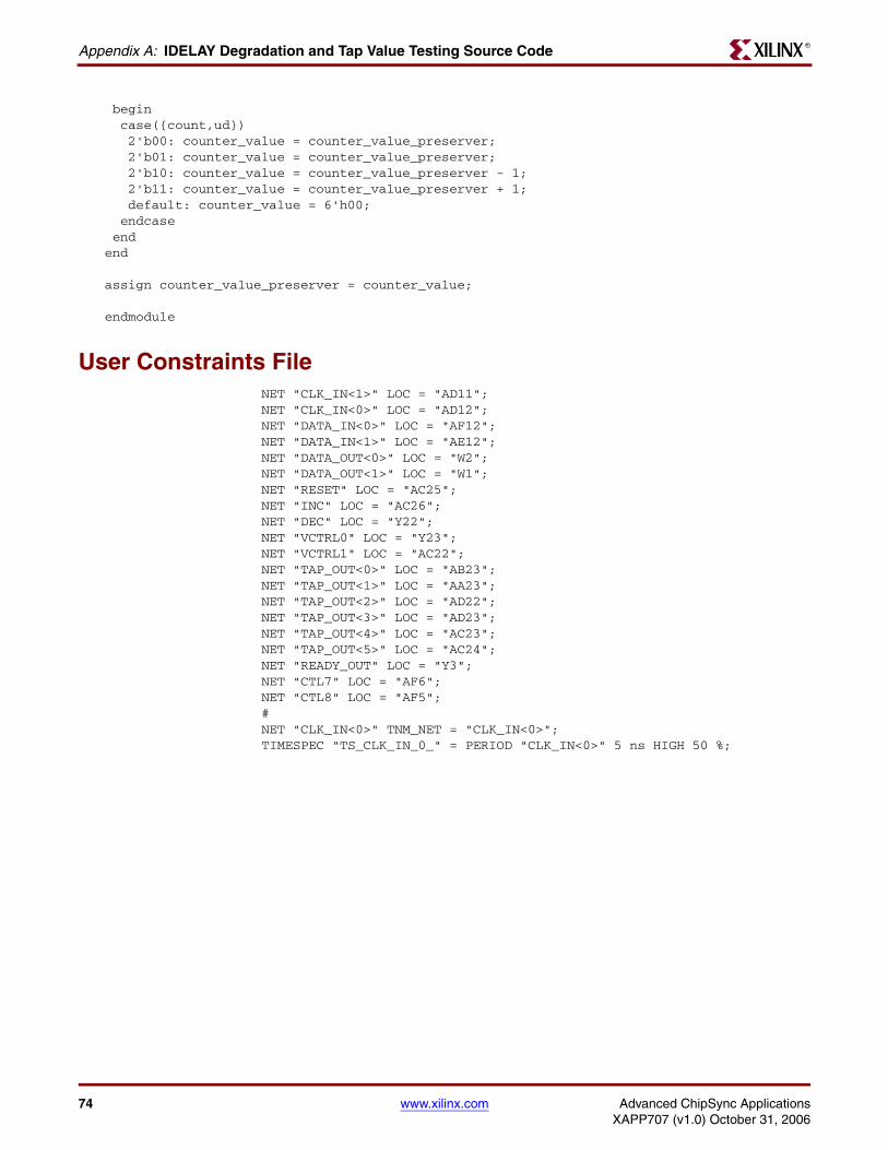
74 www.xilinx.com Advanced ChipSync ApplicationsXAPP707 (v1.0) October 31, 2006
Appendix A: IDELAY Degradation and Tap Value Testing Source CodeR
begin case({count,ud}) 2'b00: counter_value = counter_value_preserver; 2'b01: counter_value = counter_value_preserver; 2'b10: counter_value = counter_value_preserver - 1; 2'b11: counter_value = counter_value_preserver + 1; default: counter_value = 6'h00; endcase endend
assign counter_value_preserver = counter_value;
endmodule
User Constraints FileNET "CLK_IN<1>" LOC = "AD11";NET "CLK_IN<0>" LOC = "AD12";NET "DATA_IN<0>" LOC = "AF12";NET "DATA_IN<1>" LOC = "AE12";NET "DATA_OUT<0>" LOC = "W2";NET "DATA_OUT<1>" LOC = "W1";NET "RESET" LOC = "AC25";NET "INC" LOC = "AC26";NET "DEC" LOC = "Y22";NET "VCTRL0" LOC = "Y23";NET "VCTRL1" LOC = "AC22";NET "TAP_OUT<0>" LOC = "AB23";NET "TAP_OUT<1>" LOC = "AA23";NET "TAP_OUT<2>" LOC = "AD22";NET "TAP_OUT<3>" LOC = "AD23";NET "TAP_OUT<4>" LOC = "AC23";NET "TAP_OUT<5>" LOC = "AC24";NET "READY_OUT" LOC = "Y3";NET "CTL7" LOC = "AF6";NET "CTL8" LOC = "AF5";#NET "CLK_IN<0>" TNM_NET = "CLK_IN<0>";TIMESPEC "TS_CLK_IN_0_" = PERIOD "CLK_IN<0>" 5 ns HIGH 50 %;

Advanced ChipSync Applications www.xilinx.com 75XAPP707 (v1.0) October 31, 2006
R
Appendix B
IDELAY Degradation Supplemental Data
This appendix provides graphs showing IDELAY degradation over different speed grades and data rates.
Figure B-1: Eye Width for Device 6046, Speed Grade -11, 200 Mbits
X707_36_01_100705
Eye Width, SN 6046, -11, 200 Mbit
y = -0.0107x + 4.9121
4.1
4.2
4.3
4.4
4.5
4.6
4.7
4.8
4.9
5
0 10 20 30 40 50 60 70Tap
Eye
Wid
th (
ns)
PRBS23CLKPATLinear (PRBS23)Linear (CLKPAT)
10.7 ps degradation per tap
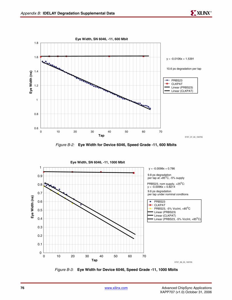
76 www.xilinx.com Advanced ChipSync ApplicationsXAPP707 (v1.0) October 31, 2006
Appendix B: IDELAY Degradation Supplemental DataR
Figure B-2: Eye Width for Device 6046, Speed Grade -11, 600 Mbits
X707_37_02_100705
Eye Width, SN 6046, -11, 600 Mbit
y = -0.0106x + 1.5391
10.6 ps degradation per tap
0.6
0.8
1
1.2
1.4
1.6
1.8
0 10 20 30 40 50 60 70Tap
Eye
Wid
th (
ns)
PRBS23CLKPATLinear (PRBS23)Linear (CLKPAT)
Figure B-3: Eye Width for Device 6046, Speed Grade -11, 1000 Mbits
X707_38_03_100705
Eye Width, SN 6046, -11, 1000 Mbit
PRBS23, nom supply, +25oC:y = -0.0096x + 0.8214
y = -0.0098x + 0.786
0
0.1
0.2
0.3
0.4
0.5
0.6
0.7
0.8
0.9
1
0 10 20 30 40 50 60 70Tap
Eye
Wid
th (
ns)
PRBS23CLKPATPRBS23, -5% VccInt, +85oCLinear (PRBS23)Linear (CLKPAT)Linear (PRBS23, -5% VccInt, +85oC)
9.6 ps degradation per tap under nominal condtions
9.8 ps degradation per tap at +85oC, -5% supply
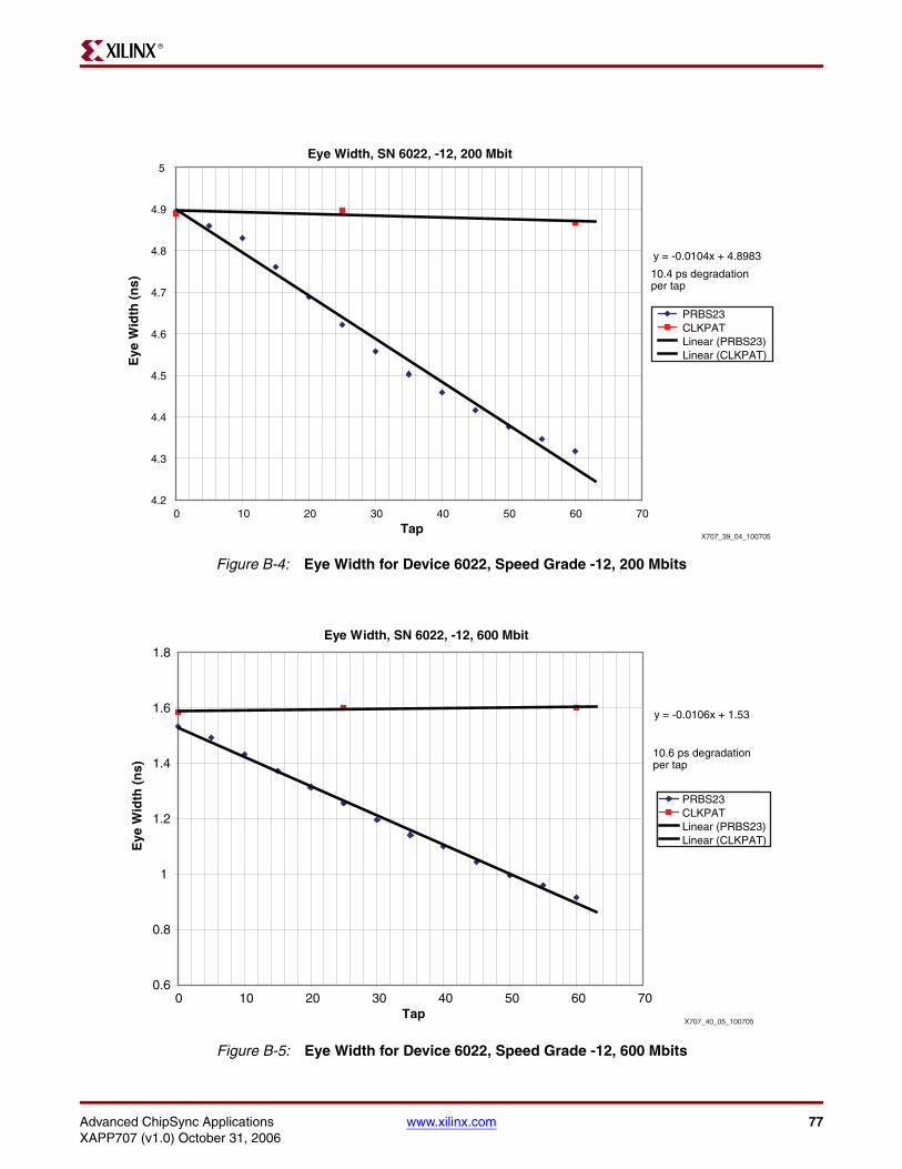
Advanced ChipSync Applications www.xilinx.com 77XAPP707 (v1.0) October 31, 2006
R
Figure B-4: Eye Width for Device 6022, Speed Grade -12, 200 Mbits
X707_39_04_100705
Eye Width, SN 6022, -12, 200 Mbit
y = -0.0104x + 4.8983
4.2
4.3
4.4
4.5
4.6
4.7
4.8
4.9
5
0 10 20 30 40 50 60 70Tap
Eye
Wid
th (
ns)
PRBS23CLKPATLinear (PRBS23)Linear (CLKPAT)
10.4 ps degradation per tap
Figure B-5: Eye Width for Device 6022, Speed Grade -12, 600 Mbits
X707_40_05_100705
Eye Width, SN 6022, -12, 600 Mbit
y = -0.0106x + 1.53
0.6
0.8
1
1.2
1.4
1.6
1.8
0 10 20 30 40 50 60 70Tap
Eye
Wid
th (
ns)
PRBS23CLKPATLinear (PRBS23)Linear (CLKPAT)
10.6 ps degradation per tap

78 www.xilinx.com Advanced ChipSync ApplicationsXAPP707 (v1.0) October 31, 2006
Appendix B: IDELAY Degradation Supplemental DataR
Figure B-6: Eye Width for Device 6022, Speed Grade -12, 1000 Mbits
X707_41_06_100705
Eye Width, SN 6017, -12, 1000 Mbit
y = -0.0086x + 0.8065
y = -0.0091x + 0.78
0
0.1
0.2
0.3
0.4
0.5
0.6
0.7
0.8
0.9
1
0 10 20 30 40 50 60 70
Tap
Eye
Wid
th (
ns)
PRBS23CLKPATPRBS23, -5% VccInt, +85oCLinear (CLKPAT)Linear (PRBS23)Linear (PRBS23, -5% VccInt, +85oC)
8.6 ps degradation per tap under nominal conditions
9.1 ps degradation per tap at +85oC, -5% supply
Figure B-7: Eye Width for Device 001, Speed Grade -10, 200 Mbits
X707_42_07_100705
Eye Width, SN 001, -10, 200 Mbit
y = -0.0107x + 4.9017
4.1
4.2
4.3
4.4
4.5
4.6
4.7
4.8
4.9
5
0 10 20 30 40 50 60 70Tap
Eye
Wid
th (
ns)
PRBS23CLKPATLinear (PRBS23)Linear (CLKPAT)
10.7 ps degradation per tap
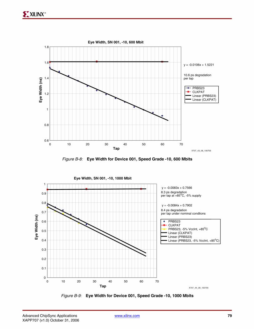
Advanced ChipSync Applications www.xilinx.com 79XAPP707 (v1.0) October 31, 2006
R
Figure B-8: Eye Width for Device 001, Speed Grade -10, 600 Mbits
X707_43_08_100705
Eye Width, SN 001, -10, 600 Mbit
y = -0.0106x + 1.5221
0.6
0.8
1
1.2
1.4
1.6
1.8
0 10 20 30 40 50 60 70Tap
Eye
Wid
th (
ns)
PRBS23CLKPATLinear (PRBS23)Linear (CLKPAT)
10.6 ps degradation per tap
Figure B-9: Eye Width for Device 001, Speed Grade -10, 1000 Mbits
X707_44_09_100705
Eye Width, SN 001, -10, 1000 Mbit
y = -0.0084x + 0.7902
y = -0.0083x + 0.7566
0
0.1
0.2
0.3
0.4
0.5
0.6
0.7
0.8
0.9
1
0 10 20 30 40 50 60 70
Tap
Eye
Wid
th (
ns)
PRBS23CLKPATPRBS23, -5% VccInt, +85oCLinear (CLKPAT)Linear (PRBS23)Linear (PRBS23, -5% VccInt, +85oC)
8.4 ps degradation per tap under nominal condtions
8.3 ps degradation per tap at +85oC, -5% supply

80 www.xilinx.com Advanced ChipSync ApplicationsXAPP707 (v1.0) October 31, 2006
Appendix B: IDELAY Degradation Supplemental DataR

Advanced ChipSync Applications www.xilinx.com 81XAPP707 (v1.0) October 31, 2006
R
Appendix C
IDELAY Jitter Transfer Testing Source Files
This appendix provides the source file listings for the IDELAY jitter transfer tests.
Verilog Source Code
Random Jitter Casemodule JITTER_XFER_200MHz (DATA_IN,CLK_IN,RESET,INC,DEC,VCTRL0,VCTRL1,CLK_SEL,TAP_OUT,DATA_OUT,READY_OUT,CTL7,CTL8,CLKOUT);
input [1:0] DATA_IN;input [1:0] CLK_IN;input RESET;input INC;input DEC;input VCTRL0;input VCTRL1;input CLK_SEL;
output [5:0] TAP_OUT;output [1:0] DATA_OUT;output READY_OUT;output CTL7;output CTL8;output [1:0] CLKOUT;
wire DATA_IN_BUF;

82 www.xilinx.com Advanced ChipSync ApplicationsXAPP707 (v1.0) October 31, 2006
Appendix C: IDELAY Jitter Transfer Testing Source FilesR
wire DATA_OUT_PREBUF;wire CLK_IN_BUF;wire CLK200;wire RESET_AH;wire INC_AH;wire DEC_AH;wire RDY;wire INC_DELAY;wire ICE_DELAY;wire [5:0] TAP;wire LOCKED_DCM;wire PRECLKOUT;wire CLKDCM;
reg [3:0] INC_CAPTURE;reg [3:0] DEC_CAPTURE;reg INC_PULSE;reg DEC_PULSE;
//Assignmentsassign RESET_AH = ~RESET; //active low switch inputassign READY_OUT = ~RDY; //active low LED outputassign INC_AH = ~INC; //active low switch inputassign DEC_AH = ~DEC; //active low switch inputassign CTL7 = ~VCTRL0;//output to voltage margining assign CTL8 = ~VCTRL1; //output to voltage marginingassign INC_DELAY = INC_PULSE;assign ICE_DELAY = INC_PULSE || DEC_PULSE;assign TAP_OUT[0] = ~TAP[0];assign TAP_OUT[1] = ~TAP[1];assign TAP_OUT[2] = ~TAP[2];assign TAP_OUT[3] = ~TAP[3];assign TAP_OUT[4] = ~TAP[4];assign TAP_OUT[5] = ~TAP[5];
//Data inputIBUFGDS_LVDS_25 DATIN(.O(DATA_IN_BUF), .I(DATA_IN[0]), .IB(DATA_IN[1]));
//synthesis attribute DIFF_TERM of DATIN is TRUE
//Clock inputIBUFGDS_LVDS_25 CLOCK_IN(.O(CLK_IN_BUF), .I(CLK_IN[0]), .IB(CLK_IN[1]));
DCM_ADV DCM_TX(.CLK0(CLKDCM),.CLK180(),.CLK270(),.CLK2X(),.CLK2X180(),

Advanced ChipSync Applications www.xilinx.com 83XAPP707 (v1.0) October 31, 2006
Verilog Source CodeR
.CLK90(),
.CLKDV(),
.CLKFX(),
.CLKFX180(),
.DO(), .DRDY(),.LOCKED(LOCKED_DCM),.CLKFB(CLK200),.CLKIN(CLK_IN_BUF),.DADDR(),
.DCLK(), .DEN(), .DI(), .DWE(), .PSCLK(), .PSEN(), .PSINCDEC(),.RST(RESET_AH));
// synthesis attribute CLKDV_DIVIDE of DCM_TX is 2.0// synthesis attribute CLKIN_DIVIDE_BY_2 of DCM_TX is FALSE// synthesis attribute CLK_FEEDBACK of DCM_TX is 1X// synthesis attribute DFS_FREQUENCY_MODE of DCM_TX is HIGH// synthesis attribute DLL_FREQUENCY_MODE of DCM_TX is HIGH// synthesis attribute FACTORY_JF of DCM_TX is 16'hF0F0// synthesis attribute CLKOUT_PHASE_SHIFT of DCM_TX is DIRECT// synthesis attribute PHASE_SHIFT of DCM_TX is 1000// synthesis attribute DCM_PERFORMANCE_MODE of DCM_TX is MAX_RANGE
BUFGMUX GLOBAL_CLK (.O(CLK200), .I0(CLKDCM),.I1(CLK_IN_BUF),.S(CLK_SEL));
//Clock OutputODDR CLK_OUT(.Q(PRECLKOUT), .C(CLK200), .CE(1'b1), .D1(1'b1), .D2(1'b0), .R(1'b0), .S(1'b0));
// synthesis attribute SRTYPE of CLK_OUT is ASYNC
OBUFDS_LVDS_25 CLOCKOUT(.O(CLKOUT[0]), .OB(CLKOUT[1]), .I(PRECLKOUT));

84 www.xilinx.com Advanced ChipSync ApplicationsXAPP707 (v1.0) October 31, 2006
Appendix C: IDELAY Jitter Transfer Testing Source FilesR
//IDELAYCTRL moduleIDELAYCTRL RX_IDELAYCTRL(.RDY(RDY), .REFCLK(CLK200), .RST(RESET_AH_OUT));
//IDELAY in data pathIDELAY IDLY_DATA(.O(DATA_OUT_PREBUF),.I(DATA_IN_BUF),.C(CLK200),.CE(ICE_DELAY),.INC(INC_DELAY),.RST(RESET_AH_OUT));
//synthesis attribute IOBDELAY_TYPE of IDLY_DATA is VARIABLE//synthesis attribute IOBDELAY_VALUE of IDLY_DATA is 0
//Module to assert reset for 16 cycles of CLK200 domain. Removes unpredictable button effectsrst_machine RST_IDLY_MACHINE(.CLK_generic(CLK200),.RST_stimulus(LOCKED_DCM),.IRDY(1'b1),.DOMAIN_RST(RESET_AH_OUT));
//Data outputOBUFDS_LVDS_25 DATOUT(.O(DATA_OUT[0]), .OB(DATA_OUT[1]), .I(DATA_OUT_PREBUF));
//Increment pulse capture to shorten each pulse to one clock cyclealways @(posedge CLK200) begin : Remove_Metastability_RxClock // asynchronous entry point INC_CAPTURE[0] <= INC_AH; DEC_CAPTURE[0] <= DEC_AH; // metastable flip-flops begin : cascade_rx integer I; for(I = 0; I <= 3 - 1; I = I + 1) begin : Rx_meta_FF INC_CAPTURE[I + 1] <= INC_CAPTURE[I]; DEC_CAPTURE[I + 1] <= DEC_CAPTURE[I]; end end // produce one pulse only INC_PULSE <= INC_CAPTURE[2] & ~INC_CAPTURE[3]; DEC_PULSE <= DEC_CAPTURE[2] & ~DEC_CAPTURE[3]; end //Produce flag when tap count reaches 64
Advanced ChipSync Applications www.xilinx.com 85XAPP707 (v1.0) October 31, 2006
Verilog Source CodeR
count_to_64 TAP_COUNTER(.clk(CLK200), .rst(RESET_AH_OUT), .count(ICE_DELAY), .ud(INC_DELAY), .counter_value(TAP));
endmodule
module rst_machine ( CLK_generic, RST_stimulus, IRDY, DOMAIN_RST ); input CLK_generic; input RST_stimulus; input IRDY; output DOMAIN_RST; reg DOMAIN_RST; reg COUNT; reg [1:0] CURRENT_STATE, NEXT_STATE; wire [3:0] COUNT_VALUE; count_to_16 machine_counter(.clk(CLK_generic), .rst(RST_stimulus),.count(COUNT), .counter_value(COUNT_VALUE)); always@(posedge CLK_generic or posedge RST_stimulus) begin if(RST_stimulus == 1'b1) begin //Initial Values CURRENT_STATE = 2'b00; end else begin //Transition Values CURRENT_STATE = NEXT_STATE; end end always@(IRDY or COUNT_VALUE or CURRENT_STATE) begin case(CURRENT_STATE) 2'b00: begin //While DCM is not locked, remain in this state DOMAIN_RST = 1'b0; COUNT = 1'b0; if(IRDY == 1'b1) NEXT_STATE = 2'b01; else
86 www.xilinx.com Advanced ChipSync ApplicationsXAPP707 (v1.0) October 31, 2006
Appendix C: IDELAY Jitter Transfer Testing Source FilesR
NEXT_STATE = 2'b00; end 2'b01: begin //Start of DOMAIN_RST and hold for 16 clock cycles. DOMAIN_RST = 1'b1; COUNT = 1'b1; if(IRDY == 1'b0) NEXT_STATE = 2'b00; else if(COUNT_VALUE != 4'hF) NEXT_STATE = 2'b01; else if(COUNT_VALUE == 4'hF) NEXT_STATE = 2'b10; end 2'b10: begin DOMAIN_RST = 1'b0; COUNT = 1'b0; if(IRDY == 1'b0) NEXT_STATE = 2'b00; else NEXT_STATE = 2'b10; end default: begin DOMAIN_RST = 1'b0; COUNT = 1'b0; NEXT_STATE = 2'b00; end endcase end endmodule
module count_to_16(clk, rst, count, counter_value);
//This module counts from 0 to 16
input clk, rst, count;output [3:0] counter_value;
reg [3:0] counter_value_preserver/*synthesis syn_noprune = 1*/;
assign counter_value = (count) ? counter_value_preserver + 1 : 4'h0;
always@(posedge clk or posedge rst) if(rst == 1'b1) counter_value_preserver = 4'h0; else counter_value_preserver = counter_value;
endmodule
module count_to_64(clk, rst, count, ud, counter_value);
//This module counts up/down between 0 to 128
Advanced ChipSync Applications www.xilinx.com 87XAPP707 (v1.0) October 31, 2006
Verilog Source CodeR
input clk, rst, count, ud;output [5:0] counter_value;
wire [5:0] counter_value_preserver;reg [5:0] counter_value/*synthesis syn_noprune = 1*/;
always@(posedge clk or posedge rst)beginif(rst == 1'b1) counter_value = 6'h00;else begin case({count,ud}) 2'b00: counter_value = counter_value_preserver; 2'b01: counter_value = counter_value_preserver; 2'b10: counter_value = counter_value_preserver - 1; 2'b11: counter_value = counter_value_preserver + 1; default: counter_value = 6'h00; endcase endend
assign counter_value_preserver = counter_value;
endmodule
Deterministic Jitter Casemodule JITTER_XFER_200MHz_deterministic (DATA_IN,CLK_IN,RESET,INC,DEC,VCTRL0,VCTRL1,CLK_SEL,TAP_OUT,DATA_OUT,READY_OUT,CTL7,CTL8,CLKOUT);
input [1:0] DATA_IN;input [1:0] CLK_IN;input RESET;input INC;input DEC;input VCTRL0;input VCTRL1;input CLK_SEL;
output [5:0] TAP_OUT;output [1:0] DATA_OUT;
88 www.xilinx.com Advanced ChipSync ApplicationsXAPP707 (v1.0) October 31, 2006
Appendix C: IDELAY Jitter Transfer Testing Source FilesR
output READY_OUT;output CTL7;output CTL8;output [1:0] CLKOUT;
wire DATA_IN_BUF;wire DATA_OUT_PREBUF;wire CLK_IN_BUF;wire CLK200;wire RESET_AH;wire INC_AH;wire DEC_AH;wire RDY;wire INC_DELAY;wire ICE_DELAY;wire [5:0] TAP;wire LOCKED_DCM;wire PRECLKOUT;wire CLKDCM;
reg [3:0] INC_CAPTURE;reg [3:0] DEC_CAPTURE;reg INC_PULSE;reg DEC_PULSE;
//Assignmentsassign RESET_AH = ~RESET; //active low switch inputassign READY_OUT = ~RDY; //active low LED outputassign INC_AH = ~INC; //active low switch inputassign DEC_AH = ~DEC; //active low switch inputassign CTL7 = ~VCTRL0;//output to voltage margining assign CTL8 = ~VCTRL1; //output to voltage marginingassign INC_DELAY = INC_PULSE;assign ICE_DELAY = INC_PULSE || DEC_PULSE;assign TAP_OUT[0] = ~TAP[0];assign TAP_OUT[1] = ~TAP[1];assign TAP_OUT[2] = ~TAP[2];assign TAP_OUT[3] = ~TAP[3];assign TAP_OUT[4] = ~TAP[4];assign TAP_OUT[5] = ~TAP[5];
//Data inputIBUFGDS_LVDS_25 DATIN(.O(DATA_IN_BUF), .I(DATA_IN[0]), .IB(DATA_IN[1]));
//synthesis attribute DIFF_TERM of DATIN is TRUE
//Clock inputIBUFGDS_LVDS_25 CLOCK_IN(.O(CLK_IN_BUF), .I(CLK_IN[0]), .IB(CLK_IN[1]));

Advanced ChipSync Applications www.xilinx.com 89XAPP707 (v1.0) October 31, 2006
Verilog Source CodeR
DCM_ADV DCM_TX(.CLK0(CLK_dummy),.CLK180(),.CLK270(),.CLK2X(),.CLK2X180(),.CLK90(),.CLKDV(),.CLKFX(CLKDCM),.CLKFX180(),.DO(),
.DRDY(),.LOCKED(LOCKED_DCM),.CLKFB(CLK_dummy_out),.CLKIN(CLK_IN_BUF),.DADDR(),
.DCLK(), .DEN(), .DI(), .DWE(), .PSCLK(), .PSEN(), .PSINCDEC(),.RST(RESET_AH));
// synthesis attribute CLKDV_DIVIDE of DCM_TX is 2.0// synthesis attribute CLKIN_DIVIDE_BY_2 of DCM_TX is FALSE// synthesis attribute CLK_FEEDBACK of DCM_TX is 1X// synthesis attribute DFS_FREQUENCY_MODE of DCM_TX is HIGH// synthesis attribute DLL_FREQUENCY_MODE of DCM_TX is HIGH// synthesis attribute FACTORY_JF of DCM_TX is 16'hF0F0// synthesis attribute CLKOUT_PHASE_SHIFT of DCM_TX is DIRECT// synthesis attribute PHASE_SHIFT of DCM_TX is 1000// synthesis attribute DCM_PERFORMANCE_MODE of DCM_TX is MAX_RANGE// synthesis attribute CLKFX_MULTIPLY of DCM_TX is 20// synthesis attribute CLKFX_DIVIDE of DCM_TX is 20
BUFGMUX GLOBAL_CLK (.O(CLK200), .I0(CLKDCM),.I1(CLK_IN_BUF),.S(CLK_SEL));
BUFG CLOCK_DUMMY (.O(CLK_dummy_out), .I(CLK_dummy));
//Clock OutputODDR CLK_OUT(.Q(PRECLKOUT), .C(CLK200), .CE(1'b1), .D1(1'b1), .D2(1'b0), .R(1'b0), .S(1'b0)

90 www.xilinx.com Advanced ChipSync ApplicationsXAPP707 (v1.0) October 31, 2006
Appendix C: IDELAY Jitter Transfer Testing Source FilesR
);
// synthesis attribute SRTYPE of CLK_OUT is ASYNC
OBUFDS_LVDS_25 CLOCKOUT(.O(CLKOUT[0]), .OB(CLKOUT[1]), .I(PRECLKOUT));
//IDELAYCTRL moduleIDELAYCTRL RX_IDELAYCTRL(.RDY(RDY), .REFCLK(CLK200), .RST(RESET_AH_OUT));
//IDELAY in data pathIDELAY IDLY_DATA(.O(DATA_OUT_PREBUF),.I(DATA_IN_BUF),.C(CLK200),.CE(ICE_DELAY),.INC(INC_DELAY),.RST(RESET_AH_OUT));
//synthesis attribute IOBDELAY_TYPE of IDLY_DATA is VARIABLE//synthesis attribute IOBDELAY_VALUE of IDLY_DATA is 0
//Module to assert reset for 16 cycles of CLK200 domain. Removes unpredictable button effectsrst_machine RST_IDLY_MACHINE(.CLK_generic(CLK200),.RST_stimulus(LOCKED_DCM),.IRDY(1'b1),.DOMAIN_RST(RESET_AH_OUT));
//Data outputOBUFDS_LVDS_25 DATOUT(.O(DATA_OUT[0]), .OB(DATA_OUT[1]), .I(DATA_OUT_PREBUF));
//Increment pulse capture to shorten each pulse to one clock cyclealways @(posedge CLK200) begin : Remove_Metastability_RxClock // asynchronous entry point INC_CAPTURE[0] <= INC_AH; DEC_CAPTURE[0] <= DEC_AH; // metastable flip-flops begin : cascade_rx integer I; for(I = 0; I <= 3 - 1; I = I + 1) begin : Rx_meta_FF

Advanced ChipSync Applications www.xilinx.com 91XAPP707 (v1.0) October 31, 2006
Verilog Source CodeR
INC_CAPTURE[I + 1] <= INC_CAPTURE[I]; DEC_CAPTURE[I + 1] <= DEC_CAPTURE[I]; end end // produce one pulse only INC_PULSE <= INC_CAPTURE[2] & ~INC_CAPTURE[3]; DEC_PULSE <= DEC_CAPTURE[2] & ~DEC_CAPTURE[3]; end //Produce flag when tap count reaches 64count_to_64 TAP_COUNTER(.clk(CLK200), .rst(RESET_AH_OUT), .count(ICE_DELAY), .ud(INC_DELAY), .counter_value(TAP));
endmodule
module rst_machine ( CLK_generic, RST_stimulus, IRDY, DOMAIN_RST ); input CLK_generic; input RST_stimulus; input IRDY; output DOMAIN_RST; reg DOMAIN_RST; reg COUNT; reg [1:0] CURRENT_STATE, NEXT_STATE; wire [3:0] COUNT_VALUE; count_to_16 machine_counter(.clk(CLK_generic), .rst(RST_stimulus),.count(COUNT), .counter_value(COUNT_VALUE)); always@(posedge CLK_generic or posedge RST_stimulus) begin if(RST_stimulus == 1'b1) begin //Initial Values CURRENT_STATE = 2'b00; end else begin //Transition Values CURRENT_STATE = NEXT_STATE; end end

92 www.xilinx.com Advanced ChipSync ApplicationsXAPP707 (v1.0) October 31, 2006
Appendix C: IDELAY Jitter Transfer Testing Source FilesR
always@(IRDY or COUNT_VALUE or CURRENT_STATE) begin case(CURRENT_STATE) 2'b00: begin //While DCM is not locked, remain in this state DOMAIN_RST = 1'b0; COUNT = 1'b0; if(IRDY == 1'b1) NEXT_STATE = 2'b01; else NEXT_STATE = 2'b00; end 2'b01: begin //Start of DOMAIN_RST and hold for 16 clock cycles. DOMAIN_RST = 1'b1; COUNT = 1'b1; if(IRDY == 1'b0) NEXT_STATE = 2'b00; else if(COUNT_VALUE != 4'hF) NEXT_STATE = 2'b01; else if(COUNT_VALUE == 4'hF) NEXT_STATE = 2'b10; end 2'b10: begin DOMAIN_RST = 1'b0; COUNT = 1'b0; if(IRDY == 1'b0) NEXT_STATE = 2'b00; else NEXT_STATE = 2'b10; end default: begin DOMAIN_RST = 1'b0; COUNT = 1'b0; NEXT_STATE = 2'b00; end endcase end endmodule
module count_to_16(clk, rst, count, counter_value);
//This module counts from 0 to 16
input clk, rst, count;output [3:0] counter_value;
reg [3:0] counter_value_preserver/*synthesis syn_noprune = 1*/;
assign counter_value = (count) ? counter_value_preserver + 1 : 4'h0;
always@(posedge clk or posedge rst) if(rst == 1'b1) counter_value_preserver = 4'h0;

Advanced ChipSync Applications www.xilinx.com 93XAPP707 (v1.0) October 31, 2006
User Constraints FileR
else counter_value_preserver = counter_value;
endmodule
module count_to_64(clk, rst, count, ud, counter_value);
//This module counts up/down between 0 to 128
input clk, rst, count, ud;output [5:0] counter_value;
wire [5:0] counter_value_preserver;reg [5:0] counter_value/*synthesis syn_noprune = 1*/;
always@(posedge clk or posedge rst)beginif(rst == 1'b1) counter_value = 6'h00;else begin case({count,ud}) 2'b00: counter_value = counter_value_preserver; 2'b01: counter_value = counter_value_preserver; 2'b10: counter_value = counter_value_preserver - 1; 2'b11: counter_value = counter_value_preserver + 1; default: counter_value = 6'h00; endcase endend
assign counter_value_preserver = counter_value;
endmodule
User Constraints FileThe User Constraints file listing applies to both random and deterministic jitter cases.
NET "CLK_IN<1>" LOC = "AD11";NET "CLK_IN<0>" LOC = "AD12";NET "DATA_IN<0>" LOC = "AF12";NET "DATA_IN<1>" LOC = "AE12";NET "DATA_OUT<0>" LOC = "W2";NET "DATA_OUT<1>" LOC = "W1";NET "RESET" LOC = "AC25";NET "INC" LOC = "AC26";NET "DEC" LOC = "Y22";NET "VCTRL0" LOC = "Y23";NET "VCTRL1" LOC = "AC22";NET "CLK_SEL" LOC = "AB22";#NET "CLKDCM_FROMIO" LOC = "AC11";NET "TAP_OUT<0>" LOC = "AB23";NET "TAP_OUT<1>" LOC = "AA23";NET "TAP_OUT<2>" LOC = "AD22";NET "TAP_OUT<3>" LOC = "AD23";NET "TAP_OUT<4>" LOC = "AC23";
94 www.xilinx.com Advanced ChipSync ApplicationsXAPP707 (v1.0) October 31, 2006
Appendix C: IDELAY Jitter Transfer Testing Source FilesR
NET "TAP_OUT<5>" LOC = "AC24";NET "READY_OUT" LOC = "Y3";NET "CTL7" LOC = "AF6";NET "CTL8" LOC = "AF5";NET "CLKOUT<0>" LOC = "J26";NET "CLKOUT<1>" LOC = "J25";#NET "CLKDCM" LOC = "Y26";#NET "CLK_IN<0>" TNM_NET = "CLK_IN<0>";TIMESPEC "TS_CLK_IN_0_" = PERIOD "CLK_IN<0>" 5 ns HIGH 50 %;

Advanced ChipSync Applications www.xilinx.com 95XAPP707 (v1.0) October 31, 2006
R
Appendix D
IDELAYCTRL Alternate Reference Clock Frequencies Source Code
This appendix lists the source files for IDELAYCTRL alternate reference clock frequency tests.
Verilog Source Codemodule ALTERNATE_REFCLK_FREQ_TEST (DATA_IN,CLK_IN,RESET,INC,DEC,VCTRL0,VCTRL1,TAP_OUT,DATA_OUT,READY_OUT,CTL7,CTL8);
input [1:0] DATA_IN;input [1:0] CLK_IN;input RESET;input INC;input DEC;input VCTRL0;input VCTRL1;
output [5:0] TAP_OUT;output [1:0] DATA_OUT;output READY_OUT;output CTL7;output CTL8;
wire DATA_IN_BUF;wire DATA_OUT_PREBUF;wire CLK_IN_BUF;wire CLK200;wire RESET_AH;wire INC_AH;wire DEC_AH;

96 www.xilinx.com Advanced ChipSync ApplicationsXAPP707 (v1.0) October 31, 2006
Appendix D: IDELAYCTRL Alternate Reference Clock Frequencies Source Code R
wire RDY;wire INC_DELAY;wire ICE_DELAY;wire [5:0] TAP;wire IDLYCTRL_ZERO;
reg [3:0] INC_CAPTURE;reg [3:0] DEC_CAPTURE;reg INC_PULSE;reg DEC_PULSE;
//Assignmentsassign RESET_AH = ~RESET; //active low switch inputassign READY_OUT = ~RDY; //active low LED outputassign INC_AH = ~INC; //active low switch inputassign DEC_AH = ~DEC; //active low switch inputassign CTL7 = ~VCTRL0;//output to voltage margining assign CTL8 = ~VCTRL1; //output to voltage marginingassign INC_DELAY = INC_PULSE;assign ICE_DELAY = INC_PULSE || DEC_PULSE;assign TAP_OUT[0] = ~TAP[0];assign TAP_OUT[1] = ~TAP[1];assign TAP_OUT[2] = ~TAP[2];assign TAP_OUT[3] = ~TAP[3];assign TAP_OUT[4] = ~TAP[4];assign TAP_OUT[5] = ~TAP[5];
//Data inputIBUFGDS_LVDS_25 DATIN(.O(DATA_IN_BUF), .I(DATA_IN[0]), .IB(DATA_IN[1]));
//synthesis attribute DIFF_TERM of DATIN is TRUE
//Clock inputIBUFGDS_LVDS_25 CLOCK_IN(.O(CLK_IN_BUF), .I(CLK_IN[0]), .IB(CLK_IN[1]));
BUFG GLOBAL_CLK (.O(CLK200), .I(CLK_IN_BUF));
//IDELAYCTRL moduleIDELAYCTRL RX_IDELAYCTRL(.RDY(RDY), .REFCLK(IDLYCTRL_ZERO), .RST(RESET_AH_OUT));BUFG DUMMY_ZERO(.O(IDLYCTRL_ZERO),.I(VCTRL0));
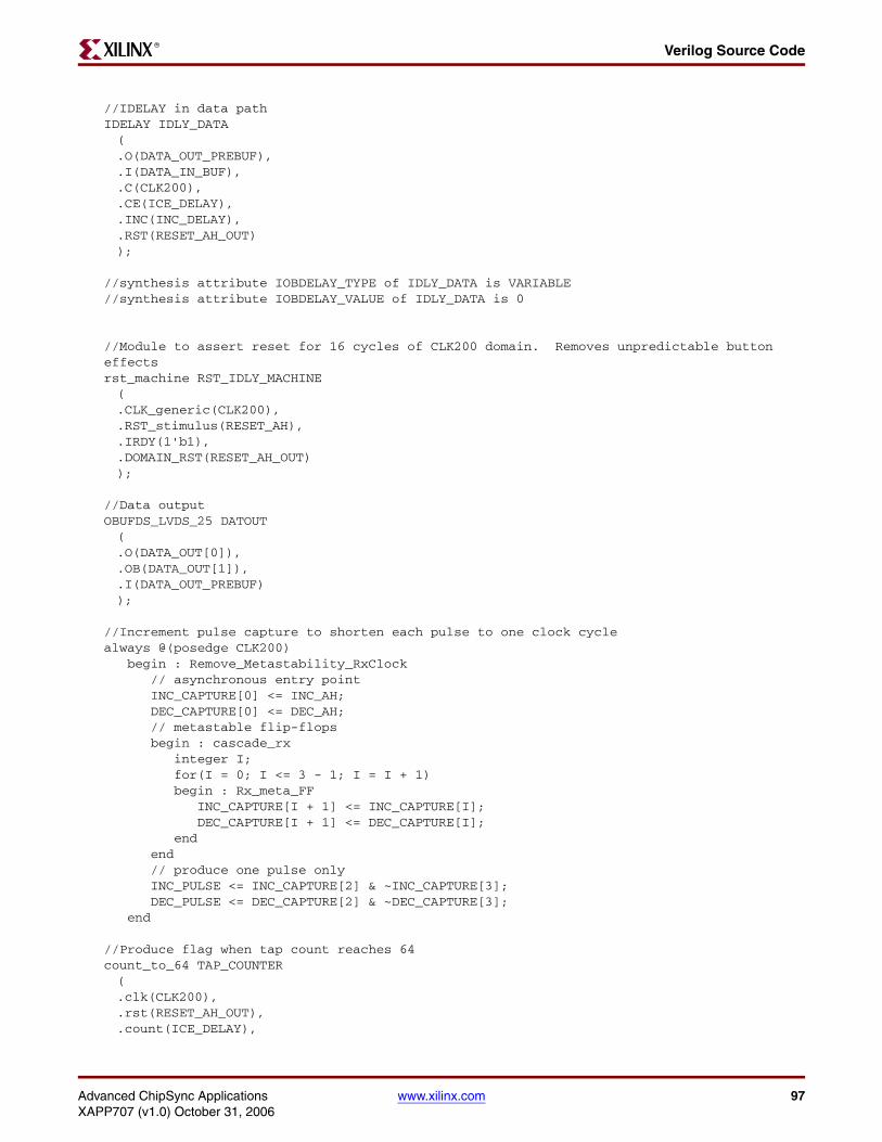
Advanced ChipSync Applications www.xilinx.com 97XAPP707 (v1.0) October 31, 2006
Verilog Source CodeR
//IDELAY in data pathIDELAY IDLY_DATA(.O(DATA_OUT_PREBUF),.I(DATA_IN_BUF),.C(CLK200),.CE(ICE_DELAY),.INC(INC_DELAY),.RST(RESET_AH_OUT));
//synthesis attribute IOBDELAY_TYPE of IDLY_DATA is VARIABLE//synthesis attribute IOBDELAY_VALUE of IDLY_DATA is 0
//Module to assert reset for 16 cycles of CLK200 domain. Removes unpredictable button effectsrst_machine RST_IDLY_MACHINE(.CLK_generic(CLK200),.RST_stimulus(RESET_AH),.IRDY(1'b1),.DOMAIN_RST(RESET_AH_OUT));
//Data outputOBUFDS_LVDS_25 DATOUT(.O(DATA_OUT[0]), .OB(DATA_OUT[1]), .I(DATA_OUT_PREBUF));
//Increment pulse capture to shorten each pulse to one clock cyclealways @(posedge CLK200) begin : Remove_Metastability_RxClock // asynchronous entry point INC_CAPTURE[0] <= INC_AH; DEC_CAPTURE[0] <= DEC_AH; // metastable flip-flops begin : cascade_rx integer I; for(I = 0; I <= 3 - 1; I = I + 1) begin : Rx_meta_FF INC_CAPTURE[I + 1] <= INC_CAPTURE[I]; DEC_CAPTURE[I + 1] <= DEC_CAPTURE[I]; end end // produce one pulse only INC_PULSE <= INC_CAPTURE[2] & ~INC_CAPTURE[3]; DEC_PULSE <= DEC_CAPTURE[2] & ~DEC_CAPTURE[3]; end //Produce flag when tap count reaches 64count_to_64 TAP_COUNTER(.clk(CLK200), .rst(RESET_AH_OUT), .count(ICE_DELAY),

98 www.xilinx.com Advanced ChipSync ApplicationsXAPP707 (v1.0) October 31, 2006
Appendix D: IDELAYCTRL Alternate Reference Clock Frequencies Source Code R
.ud(INC_DELAY),
.counter_value(TAP));
endmodule
module rst_machine ( CLK_generic, RST_stimulus, IRDY, DOMAIN_RST ); input CLK_generic; input RST_stimulus; input IRDY; output DOMAIN_RST; reg DOMAIN_RST; reg COUNT; reg [1:0] CURRENT_STATE, NEXT_STATE; wire [3:0] COUNT_VALUE; count_to_16 machine_counter(.clk(CLK_generic), .rst(RST_stimulus),.count(COUNT), .counter_value(COUNT_VALUE)); always@(posedge CLK_generic or posedge RST_stimulus) begin if(RST_stimulus == 1'b1) begin //Initial Values CURRENT_STATE = 2'b00; end else begin //Transition Values CURRENT_STATE = NEXT_STATE; end end always@(IRDY or COUNT_VALUE or CURRENT_STATE) begin case(CURRENT_STATE) 2'b00: begin //While DCM is not locked, remain in this state DOMAIN_RST = 1'b0; COUNT = 1'b0; if(IRDY == 1'b1) NEXT_STATE = 2'b01; else NEXT_STATE = 2'b00; end 2'b01: begin //Start of DOMAIN_RST and hold for 16 clock cycles.

Advanced ChipSync Applications www.xilinx.com 99XAPP707 (v1.0) October 31, 2006
Verilog Source CodeR
DOMAIN_RST = 1'b1; COUNT = 1'b1; if(IRDY == 1'b0) NEXT_STATE = 2'b00; else if(COUNT_VALUE != 4'hF) NEXT_STATE = 2'b01; else if(COUNT_VALUE == 4'hF) NEXT_STATE = 2'b10; end 2'b10: begin DOMAIN_RST = 1'b0; COUNT = 1'b0; if(IRDY == 1'b0) NEXT_STATE = 2'b00; else NEXT_STATE = 2'b10; end default: begin DOMAIN_RST = 1'b0; COUNT = 1'b0; NEXT_STATE = 2'b00; end endcase end endmodule
module count_to_16(clk, rst, count, counter_value);
//This module counts from 0 to 16
input clk, rst, count;output [3:0] counter_value;
reg [3:0] counter_value_preserver/*synthesis syn_noprune = 1*/;
assign counter_value = (count) ? counter_value_preserver + 1 : 4'h0;
always@(posedge clk or posedge rst) if(rst == 1'b1) counter_value_preserver = 4'h0; else counter_value_preserver = counter_value;
endmodule
module count_to_64(clk, rst, count, ud, counter_value);
//This module counts up/down between 0 to 128
input clk, rst, count, ud;output [5:0] counter_value;
wire [5:0] counter_value_preserver;reg [5:0] counter_value/*synthesis syn_noprune = 1*/;
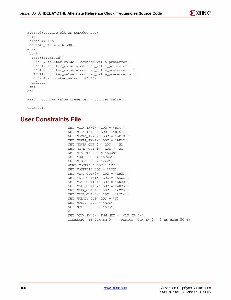
100 www.xilinx.com Advanced ChipSync ApplicationsXAPP707 (v1.0) October 31, 2006
Appendix D: IDELAYCTRL Alternate Reference Clock Frequencies Source Code R
always@(posedge clk or posedge rst)beginif(rst == 1'b1) counter_value = 6'h00;else begin case({count,ud}) 2'b00: counter_value = counter_value_preserver; 2'b01: counter_value = counter_value_preserver; 2'b10: counter_value = counter_value_preserver - 1; 2'b11: counter_value = counter_value_preserver + 1; default: counter_value = 6'h00; endcase endend
assign counter_value_preserver = counter_value;
endmodule
User Constraints FileNET "CLK_IN<1>" LOC = "B14";NET "CLK_IN<0>" LOC = "B15";NET "DATA_IN<0>" LOC = "AF12";NET "DATA_IN<1>" LOC = "AE12";NET "DATA_OUT<0>" LOC = "W2";NET "DATA_OUT<1>" LOC = "W1";NET "RESET" LOC = "AC25";NET "INC" LOC = "AC26";NET "DEC" LOC = "Y22";#NET "VCTRL0" LOC = "Y23";NET "VCTRL1" LOC = "AC22";NET "TAP_OUT<0>" LOC = "AB23";NET "TAP_OUT<1>" LOC = "AA23";NET "TAP_OUT<2>" LOC = "AD22";NET "TAP_OUT<3>" LOC = "AD23";NET "TAP_OUT<4>" LOC = "AC23";NET "TAP_OUT<5>" LOC = "AC24";NET "READY_OUT" LOC = "Y3";NET "CTL7" LOC = "AF6";NET "CTL8" LOC = "AF5";#NET "CLK_IN<0>" TNM_NET = "CLK_IN<0>";TIMESPEC "TS_CLK_IN_0_" = PERIOD "CLK_IN<0>" 5 ns HIGH 50 %;

Advanced ChipSync Applications www.xilinx.com 101XAPP707 (v1.0) October 31, 2006
R
Appendix E
ISERDES Timing Source Files
This appendix provides the ISERDES timing source file listings for Test Case 1 and Test Case 2.
Test Case 1
Verilog Source Codemodule ISERDES_TIMING_TEST
(DATA_IN,SOURCE_SYNC_CLK_IN,CLK_IN,RESET,INC,DEC,VCTRL0,VCTRL1,TAP_OUT,READY_OUT,DATA_OUT,CTL7,CTL8);
input [1:0] DATA_IN;input [1:0] SOURCE_SYNC_CLK_IN;input [1:0] CLK_IN;input RESET;input INC;input DEC;input VCTRL0;input VCTRL1;
output [5:0] TAP_OUT;output READY_OUT;output [3:0] DATA_OUT;output CTL7;output CTL8;
wire DATA_IN_BUF;wire [3:0] DATA_OUT_PREBUF;wire CLK_IN_BUF;wire CLK200;wire RESET_AH;
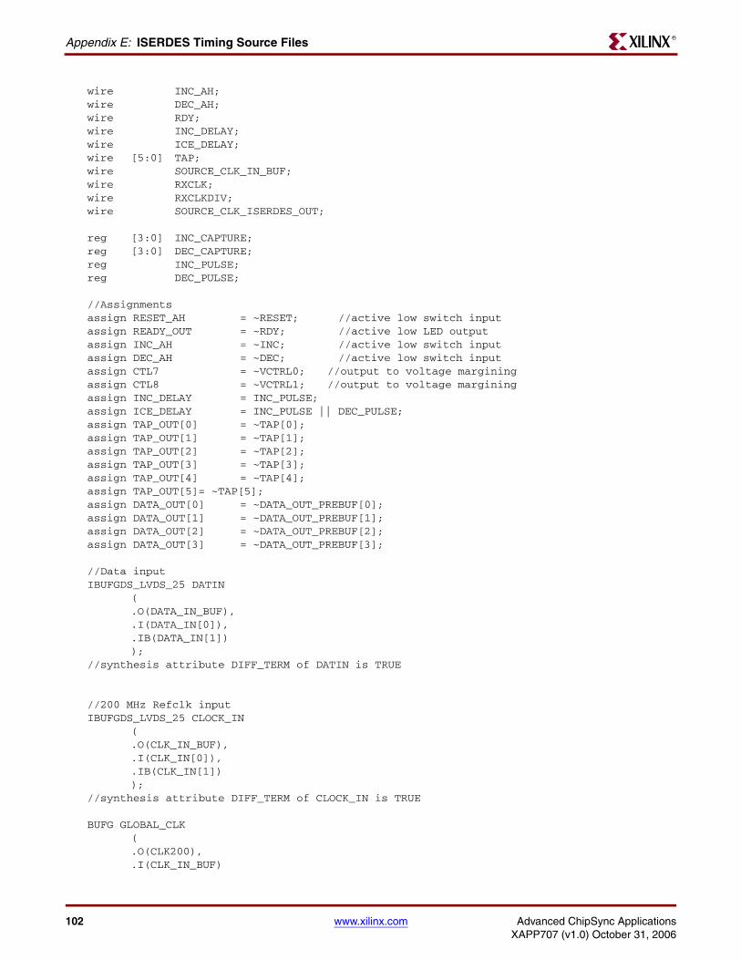
102 www.xilinx.com Advanced ChipSync ApplicationsXAPP707 (v1.0) October 31, 2006
Appendix E: ISERDES Timing Source FilesR
wire INC_AH;wire DEC_AH;wire RDY;wire INC_DELAY;wire ICE_DELAY;wire [5:0] TAP;wire SOURCE_CLK_IN_BUF;wire RXCLK;wire RXCLKDIV;wire SOURCE_CLK_ISERDES_OUT;
reg [3:0] INC_CAPTURE;reg [3:0] DEC_CAPTURE;reg INC_PULSE;reg DEC_PULSE;
//Assignmentsassign RESET_AH = ~RESET; //active low switch inputassign READY_OUT = ~RDY; //active low LED outputassign INC_AH = ~INC; //active low switch inputassign DEC_AH = ~DEC; //active low switch inputassign CTL7 = ~VCTRL0; //output to voltage margining assign CTL8 = ~VCTRL1; //output to voltage marginingassign INC_DELAY = INC_PULSE;assign ICE_DELAY = INC_PULSE || DEC_PULSE;assign TAP_OUT[0] = ~TAP[0];assign TAP_OUT[1] = ~TAP[1];assign TAP_OUT[2] = ~TAP[2];assign TAP_OUT[3] = ~TAP[3];assign TAP_OUT[4] = ~TAP[4];assign TAP_OUT[5]= ~TAP[5];assign DATA_OUT[0] = ~DATA_OUT_PREBUF[0];assign DATA_OUT[1] = ~DATA_OUT_PREBUF[1];assign DATA_OUT[2] = ~DATA_OUT_PREBUF[2];assign DATA_OUT[3] = ~DATA_OUT_PREBUF[3];
//Data inputIBUFGDS_LVDS_25 DATIN
(.O(DATA_IN_BUF), .I(DATA_IN[0]), .IB(DATA_IN[1]));
//synthesis attribute DIFF_TERM of DATIN is TRUE
//200 MHz Refclk inputIBUFGDS_LVDS_25 CLOCK_IN
(.O(CLK_IN_BUF), .I(CLK_IN[0]), .IB(CLK_IN[1]));
//synthesis attribute DIFF_TERM of CLOCK_IN is TRUE
BUFG GLOBAL_CLK (.O(CLK200), .I(CLK_IN_BUF)
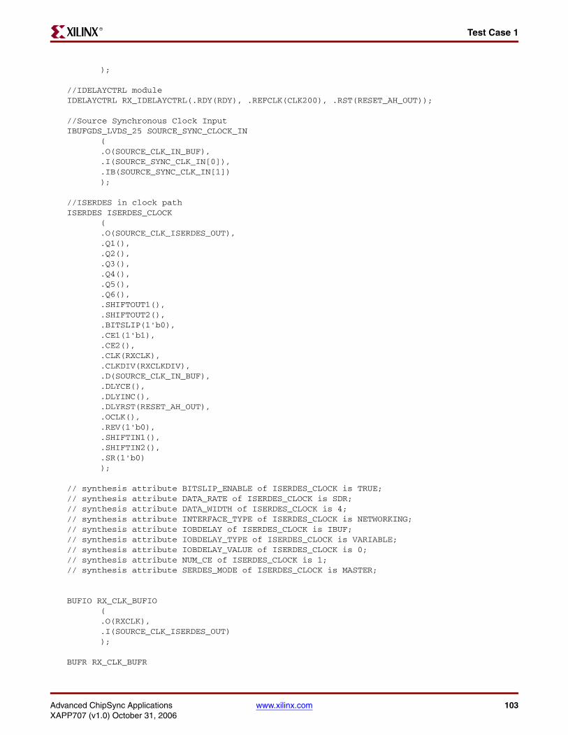
Advanced ChipSync Applications www.xilinx.com 103XAPP707 (v1.0) October 31, 2006
Test Case 1R
);
//IDELAYCTRL moduleIDELAYCTRL RX_IDELAYCTRL(.RDY(RDY), .REFCLK(CLK200), .RST(RESET_AH_OUT));
//Source Synchronous Clock InputIBUFGDS_LVDS_25 SOURCE_SYNC_CLOCK_IN
(.O(SOURCE_CLK_IN_BUF), .I(SOURCE_SYNC_CLK_IN[0]), .IB(SOURCE_SYNC_CLK_IN[1]));
//ISERDES in clock pathISERDES ISERDES_CLOCK
(.O(SOURCE_CLK_ISERDES_OUT), .Q1(), .Q2(), .Q3(), .Q4(), .Q5(), .Q6(), .SHIFTOUT1(), .SHIFTOUT2(), .BITSLIP(1'b0), .CE1(1'b1), .CE2(), .CLK(RXCLK), .CLKDIV(RXCLKDIV), .D(SOURCE_CLK_IN_BUF), .DLYCE(), .DLYINC(), .DLYRST(RESET_AH_OUT), .OCLK(), .REV(1'b0), .SHIFTIN1(), .SHIFTIN2(), .SR(1'b0));
// synthesis attribute BITSLIP_ENABLE of ISERDES_CLOCK is TRUE;// synthesis attribute DATA_RATE of ISERDES_CLOCK is SDR;// synthesis attribute DATA_WIDTH of ISERDES_CLOCK is 4;// synthesis attribute INTERFACE_TYPE of ISERDES_CLOCK is NETWORKING;// synthesis attribute IOBDELAY of ISERDES_CLOCK is IBUF;// synthesis attribute IOBDELAY_TYPE of ISERDES_CLOCK is VARIABLE;// synthesis attribute IOBDELAY_VALUE of ISERDES_CLOCK is 0;// synthesis attribute NUM_CE of ISERDES_CLOCK is 1;// synthesis attribute SERDES_MODE of ISERDES_CLOCK is MASTER;
BUFIO RX_CLK_BUFIO(.O(RXCLK), .I(SOURCE_CLK_ISERDES_OUT));
BUFR RX_CLK_BUFR

104 www.xilinx.com Advanced ChipSync ApplicationsXAPP707 (v1.0) October 31, 2006
Appendix E: ISERDES Timing Source FilesR
(.O(RXCLKDIV), .CE(1'b1), .CLR(1'b0), .I(RXCLK));
// synthesis attribute BUFR_DIVIDE of RX_CLK_BUFR is 4// synthesis attribute buffer_type of RXCLKDIV is none
//ISERDES in data pathISERDES ISERDES_CDR_IN00
(.O(), .Q1(DATA_OUT_PREBUF[3]), .Q2(DATA_OUT_PREBUF[2]), .Q3(DATA_OUT_PREBUF[1]), .Q4(DATA_OUT_PREBUF[0]), .Q5(), .Q6(), .SHIFTOUT1(), .SHIFTOUT2(), .BITSLIP(1'b0), .CE1(1'b1), .CE2(), .CLK(RXCLK), .CLKDIV(RXCLKDIV), .D(DATA_IN_BUF), .DLYCE(ICE_DELAY), .DLYINC(INC_DELAY), .DLYRST(RESET_AH_OUT), .OCLK(), .REV(1'b0), .SHIFTIN1(), .SHIFTIN2(), .SR(RESET_AH_OUT));
// synthesis attribute BITSLIP_ENABLE of ISERDES_CDR_IN00 is TRUE;// synthesis attribute DATA_RATE of ISERDES_CDR_IN00 is SDR;// synthesis attribute DATA_WIDTH of ISERDES_CDR_IN00 is 4;// synthesis attribute INTERFACE_TYPE of ISERDES_CDR_IN00 is NETWORKING;// synthesis attribute IOBDELAY of ISERDES_CDR_IN00 is BOTH;// synthesis attribute IOBDELAY_TYPE of ISERDES_CDR_IN00 is VARIABLE;// synthesis attribute IOBDELAY_VALUE of ISERDES_CDR_IN00 is 0;// synthesis attribute NUM_CE of ISERDES_CDR_IN00 is 1;// synthesis attribute SERDES_MODE of ISERDES_CDR_IN00 is MASTER;
//Module to assert reset for 16 cycles of CLKDIV domain. Removes unpredictable //button effectsrst_machine RST_IDLY_MACHINE
(.CLK_generic(RXCLKDIV),.RST_stimulus(RESET_AH),.IRDY(1'b1),.DOMAIN_RST(RESET_AH_OUT));
Advanced ChipSync Applications www.xilinx.com 105XAPP707 (v1.0) October 31, 2006
Test Case 1R
//Increment pulse capture to shorten each pulse to one clock cyclealways @(posedge RXCLKDIV) begin : Remove_Metastability_RxClock // asynchronous entry point INC_CAPTURE[0] <= INC_AH; DEC_CAPTURE[0] <= DEC_AH; // metastable flip-flops begin : cascade_rx integer I; for(I = 0; I <= 3 - 1; I = I + 1) begin : Rx_meta_FF INC_CAPTURE[I + 1] <= INC_CAPTURE[I]; DEC_CAPTURE[I + 1] <= DEC_CAPTURE[I]; end end // produce one pulse only INC_PULSE <= INC_CAPTURE[2] & ~INC_CAPTURE[3]; DEC_PULSE <= DEC_CAPTURE[2] & ~DEC_CAPTURE[3]; end //Produce flag when tap count reaches 64count_to_64 TAP_COUNTER
(.clk(RXCLKDIV), .rst(RESET_AH_OUT), .count(ICE_DELAY), .ud(INC_DELAY), .counter_value(TAP));
endmodule
module rst_machine ( CLK_generic, RST_stimulus, IRDY, DOMAIN_RST ); input CLK_generic; input RST_stimulus; input IRDY; output DOMAIN_RST; reg DOMAIN_RST; reg COUNT; reg [1:0] CURRENT_STATE, NEXT_STATE; wire [3:0] COUNT_VALUE; count_to_16 machine_counter(.clk(CLK_generic), .rst(RST_stimulus),.count(COUNT), .counter_value(COUNT_VALUE)); always@(posedge CLK_generic or posedge RST_stimulus)
106 www.xilinx.com Advanced ChipSync ApplicationsXAPP707 (v1.0) October 31, 2006
Appendix E: ISERDES Timing Source FilesR
begin if(RST_stimulus == 1'b1) begin //Initial Values CURRENT_STATE = 2'b00; end else begin //Transition Values CURRENT_STATE = NEXT_STATE; end end always@(IRDY or COUNT_VALUE or CURRENT_STATE) begin case(CURRENT_STATE) 2'b00: begin //While DCM is not locked, remain in this state DOMAIN_RST = 1'b0; COUNT = 1'b0; if(IRDY == 1'b1) NEXT_STATE = 2'b01; else NEXT_STATE = 2'b00; end 2'b01: begin //Start of DOMAIN_RST and hold for 16 clock cycles. DOMAIN_RST = 1'b1; COUNT = 1'b1; if(IRDY == 1'b0) NEXT_STATE = 2'b00; else if(COUNT_VALUE != 4'hF) NEXT_STATE = 2'b01; else if(COUNT_VALUE == 4'hF) NEXT_STATE = 2'b10; end 2'b10: begin DOMAIN_RST = 1'b0; COUNT = 1'b0; if(IRDY == 1'b0) NEXT_STATE = 2'b00; else NEXT_STATE = 2'b10; end default: begin DOMAIN_RST = 1'b0; COUNT = 1'b0; NEXT_STATE = 2'b00; end endcase end endmodule
module count_to_16(clk, rst, count, counter_value);
Advanced ChipSync Applications www.xilinx.com 107XAPP707 (v1.0) October 31, 2006
Test Case 1R
//This module counts from 0 to 16
input clk, rst, count;output [3:0] counter_value;
reg [3:0] counter_value_preserver/*synthesis syn_noprune = 1*/;
assign counter_value = (count) ? counter_value_preserver + 1 : 4'h0;
always@(posedge clk or posedge rst) if(rst == 1'b1) counter_value_preserver = 4'h0; else counter_value_preserver = counter_value;
endmodule
module count_to_64(clk, rst, count, ud, counter_value);
//This module counts up/down between 0 to 128
input clk, rst, count, ud;output [5:0] counter_value;
wire [5:0] counter_value_preserver;reg [5:0] counter_value/*synthesis syn_noprune = 1*/;
always@(posedge clk or posedge rst)beginif(rst == 1'b1) counter_value = 6'h00;else begin case({count,ud}) 2'b00: counter_value = counter_value_preserver; 2'b01: counter_value = counter_value_preserver; 2'b10: counter_value = counter_value_preserver - 1; 2'b11: counter_value = counter_value_preserver + 1; default: counter_value = 6'h00; endcase endend
assign counter_value_preserver = counter_value;
endmodule
User Constraints FileNET "CLK_IN<1>" LOC = "AD11";NET "CLK_IN<0>" LOC = "AD12";NET "SOURCE_SYNC_CLK_IN<1>" LOC = "N19";NET "SOURCE_SYNC_CLK_IN<0>" LOC = "M19";NET "DATA_IN<0>" LOC = "J26";NET "DATA_IN<1>" LOC = "J25";NET "DATA_OUT<0>" LOC = "Y3";

108 www.xilinx.com Advanced ChipSync ApplicationsXAPP707 (v1.0) October 31, 2006
Appendix E: ISERDES Timing Source FilesR
NET "DATA_OUT<1>" LOC = "Y5";NET "DATA_OUT<2>" LOC = "AB3";NET "DATA_OUT<3>" LOC = "AE3";NET "RESET" LOC = "AC25";NET "INC" LOC = "AC26";NET "DEC" LOC = "Y22";NET "VCTRL0" LOC = "Y23";NET "VCTRL1" LOC = "AC22";NET "TAP_OUT<0>" LOC = "AB23";NET "TAP_OUT<1>" LOC = "AA23";NET "TAP_OUT<2>" LOC = "AD22";NET "TAP_OUT<3>" LOC = "AD23";NET "TAP_OUT<4>" LOC = "AC23";NET "TAP_OUT<5>" LOC = "AC24";NET "READY_OUT" LOC = "W1";NET "CTL7" LOC = "AF6";NET "CTL8" LOC = "AF5";#NET "SOURCE_SYNC_CLK_IN<0>" TNM_NET = "SOURCE_SYNC_CLK_IN<0>";TIMESPEC "TS_SOURCE_SYNC_CLK_IN_0_" = PERIOD "SOURCE_SYNC_CLK_IN<0>" 2.5 ns HIGH 50 %;
Timing Report Excerpt===============================================================Timing constraint: Unconstrained OFFSET IN BEFORE analysis for clock "RXCLK"
6 items analyzed, 0 timing errors detected. Offset is -0.281ns.----------------------------------------------------------------------Offset (setup paths): -0.281ns (data path - clock path + uncertainty) Source: DATA_IN<0> (PAD) Destination: ISERDES_CDR_IN00/FF0 (FF) Destination Clock: RXCLK rising at 0.000ns Data Path Delay: 2.368ns (Levels of Logic = 2) Clock Path Delay: 2.649ns (Levels of Logic = 4) Clock Uncertainty: 0.000ns
Data Path: DATA_IN<0> to ISERDES_CDR_IN00/FF0 Location Delay type Delay(ns) Physical Resource Logical Resource(s) ---------------------------------------------------------------- J26.I Tiopi 1.350 DATA_IN<0> DATA_IN<0> DATIN/IBUFDS ILOGIC_X0Y121.D net (fanout=1) 0.117 DATA_IN_BUF_PRE ILOGIC_X0Y121.CLK Tisdck_D_BOTH 0.901 DATA_OUT_PREBUF<3> DATA_DELAY ISERDES_CDR_IN00/FF0 ------------------------------------------------------------------ Total 2.368ns (2.251ns logic, 0.117ns route) (95.1% logic, 4.9% route)
Clock Path: SOURCE_SYNC_CLK_IN<1> to ISERDES_CDR_IN00/FF0 Location Delay type Delay(ns) Physical Resource Logical Resource(s) ----------------------------------------------------------------- N19.PADOUT Tiopp 1.074 SOURCE_SYNC_CLK_IN<1>

Advanced ChipSync Applications www.xilinx.com 109XAPP707 (v1.0) October 31, 2006
Test Case 1R
SOURCE_SYNC_CLK_IN<1> M19.DIFFI_IN net (fanout=1) 0.000 SOURCE_SYNC_CLOCK_IN
/SLAVEBUF.DIFFIN M19.I Tiodi 0.000 SOURCE_SYNC_CLK_IN<0> SOURCE_SYNC_CLOCK_IN/IBUFDS ILOGIC_X0Y111.D net (fanout=1) 0.108 SOURCE_CLK_IN_BUF ILOGIC_X0Y111.O Tisdo_DO_IBUF 0.903 ISERDES_CLOCK ISERDES_CLOCK BUFIO_X0Y6.I net (fanout=1) 0.001 SOURCE_CLK_ISERDES_OUT BUFIO_X0Y6.O Tbufiocko_O 0.000 RX_CLK_BUFIO RX_CLK_BUFIO ILOGIC_X0Y121.CLK net (fanout=3) 0.563 RXCLK ------------------------------------------------------------------ Total 2.649ns (1.977ns logic, 0.672ns route) (74.6% logic, 25.4% route)
----------------------------------------------------------------------
Hold Paths: Unconstrained OFFSET IN BEFORE analysis for clock "RXCLK"
----------------------------------------------------------------------Offset (hold paths): -1.259ns (data path - clock path + uncertainty) Source: DATA_IN<0> (PAD) Destination: ISERDES_CDR_IN00/FF0 (FF) Destination Clock: RXCLK rising at 0.000ns Data Path Delay: 1.872ns (Levels of Logic = 2) Clock Path Delay: 3.131ns (Levels of Logic = 3) Clock Uncertainty: 0.000ns
Data Path: DATA_IN<0> to ISERDES_CDR_IN00/FF0 Location Delay type Delay(ns) Physical Resource Logical Resource(s) ---------------------------------------------------------------- J26.I Tiopi 1.122 DATA_IN<0> DATA_IN<0> DATIN/IBUFDS ILOGIC_X0Y121.D net (fanout=1) 0.108 DATA_IN_BUF_PRE ILOGIC_X0Y121.CLK Tisdck_D_BOTH (-Th) -0.642 DATA_OUT_PREBUF<3> DATA_DELAY ISERDES_CDR_IN00/FF0 ----------------------------------------------------------------- Total 1.872ns (1.764ns logic, 0.108ns route) (94.2% logic, 5.8% route)
Clock Path: SOURCE_SYNC_CLK_IN<0> to ISERDES_CDR_IN00/FF0 Location Delay type Delay(ns) Physical Resource Logical Resource(s) ---------------------------------------------------------------- M19.I Tiopi 1.300 SOURCE_SYNC_CLK_IN<0> SOURCE_SYNC_CLK_IN<0> SOURCE_SYNC_CLOCK_IN/IBUFDS ILOGIC_X0Y111.D net (fanout=1) 0.117 SOURCE_CLK_IN_BUF ILOGIC_X0Y111.O Tisdo_DO_IBUF 0.982 ISERDES_CLOCK ISERDES_CLOCK BUFIO_X0Y6.I net (fanout=1) 0.001 SOURCE_CLK_ISERDES_OUT BUFIO_X0Y6.O Tbufiocko_O 0.000 RX_CLK_BUFIO RX_CLK_BUFIO ILOGIC_X0Y121.CLK net (fanout=3) 0.731 RXCLK -----------------------------------------------------------------

110 www.xilinx.com Advanced ChipSync ApplicationsXAPP707 (v1.0) October 31, 2006
Appendix E: ISERDES Timing Source FilesR
Total 3.131ns (2.282ns logic, 0.849ns route) (72.9% logic, 27.1% route)
----------------------------------------------------------------------
Test Case 2
Verilog Source Codemodule ISERDES_TIMING_TEST (DATA_IN,SOURCE_SYNC_CLK_IN,CLK_IN,RESET,INC,DEC,VCTRL0,VCTRL1,TAP_OUT,READY_OUT,DATA_OUT,CTL7,CTL8);
input[1:0]DATA_IN;input[1:0]SOURCE_SYNC_CLK_IN;input[1:0]CLK_IN;inputRESET;inputINC;inputDEC;inputVCTRL0;inputVCTRL1;
output[5:0]TAP_OUT;outputREADY_OUT;output[3:0]DATA_OUT;outputCTL7;outputCTL8;
wireDATA_IN_BUF;wire[3:0]DATA_OUT_PREBUF;wireCLK_IN_BUF;wireCLK200;wireRESET_AH;wireINC_AH;wireDEC_AH;wireRDY;wireINC_DELAY;wireICE_DELAY;wire[5:0]TAP;wireSOURCE_CLK_IN_BUF;wireRXCLK;wireRXCLKDIV;
reg[3:0]INC_CAPTURE;

Advanced ChipSync Applications www.xilinx.com 111XAPP707 (v1.0) October 31, 2006
Test Case 2R
reg[3:0]DEC_CAPTURE;reg INC_PULSE;reg DEC_PULSE;
//Assignmentsassign RESET_AH= ~RESET;//active low switch inputassign READY_OUT= ~RDY;//active low LED outputassign INC_AH= ~INC;//active low switch inputassign DEC_AH= ~DEC;//active low switch inputassign CTL7= ~VCTRL0;//output to voltage margining assign CTL8= ~VCTRL1; //output to voltage marginingassign INC_DELAY= INC_PULSE;assign ICE_DELAY= INC_PULSE || DEC_PULSE;assign TAP_OUT[0]= ~TAP[0];assign TAP_OUT[1]= ~TAP[1];assign TAP_OUT[2]= ~TAP[2];assign TAP_OUT[3]= ~TAP[3];assign TAP_OUT[4]= ~TAP[4];assign TAP_OUT[5]= ~TAP[5];assign DATA_OUT[0]= ~DATA_OUT_PREBUF[0];assign DATA_OUT[1]= ~DATA_OUT_PREBUF[1];assign DATA_OUT[2]= ~DATA_OUT_PREBUF[2];assign DATA_OUT[3]= ~DATA_OUT_PREBUF[3];
//Data inputIBUFGDS_LVDS_25 DATIN(.O(DATA_IN_BUF), .I(DATA_IN[0]), .IB(DATA_IN[1]));
//synthesis attribute DIFF_TERM of DATIN is TRUE
//200 MHz Refclk inputIBUFGDS_LVDS_25 CLOCK_IN(.O(CLK_IN_BUF), .I(CLK_IN[0]), .IB(CLK_IN[1]));
//synthesis attribute DIFF_TERM of CLOCK_IN is TRUE
BUFG GLOBAL_CLK (.O(CLK200), .I(CLK_IN_BUF));
//IDELAYCTRL moduleIDELAYCTRL RX_IDELAYCTRL(.RDY(RDY), .REFCLK(CLK200), .RST(RESET_AH_OUT));
//Source Synchronous Clock InputIBUFGDS_LVDS_25 SOURCE_SYNC_CLOCK_IN(.O(SOURCE_CLK_IN_BUF), .I(SOURCE_SYNC_CLK_IN[0]), .IB(SOURCE_SYNC_CLK_IN[1])

112 www.xilinx.com Advanced ChipSync ApplicationsXAPP707 (v1.0) October 31, 2006
Appendix E: ISERDES Timing Source FilesR
);
BUFIO RX_CLK_BUFIO(.O(RXCLK), .I(SOURCE_CLK_IN_BUF));
BUFR RX_CLK_BUFR(.O(RXCLKDIV), .CE(1'b1), .CLR(1'b0), .I(RXCLK));
// synthesis attribute BUFR_DIVIDE of RX_CLK_BUFR is 4// synthesis attribute buffer_type of RXCLKDIV is none
//ISERDES in data pathISERDES ISERDES_CDR_IN00(.O(), .Q1(DATA_OUT_PREBUF[3]), .Q2(DATA_OUT_PREBUF[2]), .Q3(DATA_OUT_PREBUF[1]), .Q4(DATA_OUT_PREBUF[0]), .Q5(), .Q6(), .SHIFTOUT1(), .SHIFTOUT2(), .BITSLIP(1'b0), .CE1(1'b1), .CE2(), .CLK(RXCLK), .CLKDIV(RXCLKDIV), .D(DATA_IN_BUF), .DLYCE(ICE_DELAY), .DLYINC(INC_DELAY), .DLYRST(RESET_AH_OUT), .OCLK(), .REV(1'b0), .SHIFTIN1(), .SHIFTIN2(), .SR(RESET_AH_OUT));
// synthesis attribute BITSLIP_ENABLE of ISERDES_CDR_IN00 is TRUE;// synthesis attribute DATA_RATE of ISERDES_CDR_IN00 is SDR;// synthesis attribute DATA_WIDTH of ISERDES_CDR_IN00 is 4;// synthesis attribute INTERFACE_TYPE of ISERDES_CDR_IN00 is NETWORKING;// synthesis attribute IOBDELAY of ISERDES_CDR_IN00 is BOTH;// synthesis attribute IOBDELAY_TYPE of ISERDES_CDR_IN00 is VARIABLE;// synthesis attribute IOBDELAY_VALUE of ISERDES_CDR_IN00 is 0;// synthesis attribute NUM_CE of ISERDES_CDR_IN00 is 1;// synthesis attribute SERDES_MODE of ISERDES_CDR_IN00 is MASTER;

Advanced ChipSync Applications www.xilinx.com 113XAPP707 (v1.0) October 31, 2006
Test Case 2R
//Module to assert reset for 16 cycles of CLKDIV domain. Removes unpredictable //button effectsrst_machine RST_IDLY_MACHINE(.CLK_generic(RXCLKDIV),.RST_stimulus(RESET_AH),.IRDY(1'b1),.DOMAIN_RST(RESET_AH_OUT));
//Increment pulse capture to shorten each pulse to one clock cyclealways @(posedge RXCLKDIV) begin : Remove_Metastability_RxClock // asynchronous entry point INC_CAPTURE[0] <= INC_AH; DEC_CAPTURE[0] <= DEC_AH; // metastable flip-flops begin : cascade_rx integer I; for(I = 0; I <= 3 - 1; I = I + 1) begin : Rx_meta_FF INC_CAPTURE[I + 1] <= INC_CAPTURE[I]; DEC_CAPTURE[I + 1] <= DEC_CAPTURE[I]; end end // produce one pulse only INC_PULSE <= INC_CAPTURE[2] & ~INC_CAPTURE[3]; DEC_PULSE <= DEC_CAPTURE[2] & ~DEC_CAPTURE[3]; end //Produce flag when tap count reaches 64count_to_64 TAP_COUNTER(.clk(RXCLKDIV), .rst(RESET_AH_OUT), .count(ICE_DELAY), .ud(INC_DELAY), .counter_value(TAP));
endmodule
module rst_machine ( CLK_generic, RST_stimulus, IRDY, DOMAIN_RST ); input CLK_generic; input RST_stimulus; input IRDY; output DOMAIN_RST;

114 www.xilinx.com Advanced ChipSync ApplicationsXAPP707 (v1.0) October 31, 2006
Appendix E: ISERDES Timing Source FilesR
reg DOMAIN_RST; reg COUNT; reg [1:0] CURRENT_STATE, NEXT_STATE; wire [3:0] COUNT_VALUE; count_to_16 machine_counter(.clk(CLK_generic), .rst(RST_stimulus),.count(COUNT), .counter_value(COUNT_VALUE)); always@(posedge CLK_generic or posedge RST_stimulus) begin if(RST_stimulus == 1'b1) begin //Initial Values CURRENT_STATE = 2'b00; end else begin //Transition Values CURRENT_STATE = NEXT_STATE; end end always@(IRDY or COUNT_VALUE or CURRENT_STATE) begin case(CURRENT_STATE) 2'b00: begin //While DCM is not locked, remain in this state DOMAIN_RST = 1'b0; COUNT = 1'b0; if(IRDY == 1'b1) NEXT_STATE = 2'b01; else NEXT_STATE = 2'b00; end 2'b01: begin //Start of DOMAIN_RST and hold for 16 clock cycles. DOMAIN_RST = 1'b1; COUNT = 1'b1; if(IRDY == 1'b0) NEXT_STATE = 2'b00; else if(COUNT_VALUE != 4'hF) NEXT_STATE = 2'b01; else if(COUNT_VALUE == 4'hF) NEXT_STATE = 2'b10; end 2'b10: begin DOMAIN_RST = 1'b0; COUNT = 1'b0; if(IRDY == 1'b0) NEXT_STATE = 2'b00; else NEXT_STATE = 2'b10; end default: begin

Advanced ChipSync Applications www.xilinx.com 115XAPP707 (v1.0) October 31, 2006
Test Case 2R
DOMAIN_RST = 1'b0; COUNT = 1'b0; NEXT_STATE = 2'b00; end endcase end endmodule
module count_to_16(clk, rst, count, counter_value);
//This module counts from 0 to 16
input clk, rst, count;output [3:0] counter_value;
reg [3:0] counter_value_preserver/*synthesis syn_noprune = 1*/;
assign counter_value = (count) ? counter_value_preserver + 1 : 4'h0;
always@(posedge clk or posedge rst) if(rst == 1'b1) counter_value_preserver = 4'h0; else counter_value_preserver = counter_value;
endmodule
module count_to_64(clk, rst, count, ud, counter_value);
//This module counts up/down between 0 to 128
input clk, rst, count, ud;output [5:0] counter_value;
wire [5:0] counter_value_preserver;reg [5:0] counter_value/*synthesis syn_noprune = 1*/;
always@(posedge clk or posedge rst)beginif(rst == 1'b1) counter_value = 6'h00;else begin case({count,ud}) 2'b00: counter_value = counter_value_preserver; 2'b01: counter_value = counter_value_preserver; 2'b10: counter_value = counter_value_preserver - 1; 2'b11: counter_value = counter_value_preserver + 1; default: counter_value = 6'h00; endcase endend
assign counter_value_preserver = counter_value;
endmodule

116 www.xilinx.com Advanced ChipSync ApplicationsXAPP707 (v1.0) October 31, 2006
Appendix E: ISERDES Timing Source FilesR
User Constraints FileNET "CLK_IN<1>" LOC = "AD11";NET "CLK_IN<0>" LOC = "AD12";NET "SOURCE_SYNC_CLK_IN<1>" LOC = "N19";NET "SOURCE_SYNC_CLK_IN<0>" LOC = "M19";NET "DATA_IN<0>" LOC = "J26";NET "DATA_IN<1>" LOC = "J25";NET "DATA_OUT<0>" LOC = "Y3";NET "DATA_OUT<1>" LOC = "Y5";NET "DATA_OUT<2>" LOC = "AB3";NET "DATA_OUT<3>" LOC = "AE3";NET "RESET" LOC = "AC25";NET "INC" LOC = "AC26";NET "DEC" LOC = "Y22";NET "VCTRL0" LOC = "Y23";NET "VCTRL1" LOC = "AC22";NET "TAP_OUT<0>" LOC = "AB23";NET "TAP_OUT<1>" LOC = "AA23";NET "TAP_OUT<2>" LOC = "AD22";NET "TAP_OUT<3>" LOC = "AD23";NET "TAP_OUT<4>" LOC = "AC23";NET "TAP_OUT<5>" LOC = "AC24";NET "READY_OUT" LOC = "W1";NET "CTL7" LOC = "AF6";NET "CTL8" LOC = "AF5";#NET "SOURCE_SYNC_CLK_IN<0>" TNM_NET = "SOURCE_SYNC_CLK_IN<0>";TIMESPEC "TS_SOURCE_SYNC_CLK_IN_0_" = PERIOD "SOURCE_SYNC_CLK_IN<0>" 2.5 ns HIGH 50 %;
Timing Report Excerpt======================================================================Timing constraint: Unconstrained OFFSET IN BEFORE analysis for clock "RXCLK"
4 items analyzed, 0 timing errors detected. Minimum allowable offset is 0.405ns.----------------------------------------------------------------------Offset (setup paths): 0.405ns (data path - clock path + uncertainty) Source: DATA_IN<0> (PAD) Destination: ISERDES_CDR_IN00/FF0 (FF) Destination Clock: RXCLK rising at 0.000ns Data Path Delay: 2.368ns (Levels of Logic = 2) Clock Path Delay: 1.963ns (Levels of Logic = 3) Clock Uncertainty: 0.000ns
Data Path: DATA_IN<0> to ISERDES_CDR_IN00/FF0 Location Delay type Delay(ns) Physical Resource Logical Resource(s) ---------------------------------------------------------------- J26.I Tiopi 1.350 DATA_IN<0> DATA_IN<0> DATIN/IBUFDS ILOGIC_X0Y121.D net (fanout=1) 0.117 DATA_IN_BUF_PRE ILOGIC_X0Y121.CLK Tisdck_D_BOTH 0.901 DATA_OUT_PREBUF<3> DATA_DELAY

Advanced ChipSync Applications www.xilinx.com 117XAPP707 (v1.0) October 31, 2006
Test Case 2R
ISERDES_CDR_IN00/FF0 ------------------------------------------------------------------ Total 2.368ns (2.251ns logic, 0.117ns route) (95.1% logic, 4.9% route)
Clock Path: SOURCE_SYNC_CLK_IN<1> to ISERDES_CDR_IN00/FF0 Location Delay type Delay(ns) Physical Resource Logical Resource(s) ---------------------------------------------------------------- N19.PADOUT Tiopp 1.074 SOURCE_SYNC_CLK_IN<1> SOURCE_SYNC_CLK_IN<1> M19.DIFFI_IN net (fanout=1) 0.000 SOURCE_SYNC_CLOCK_IN
/SLAVEBUF.DIFFIN M19.I Tiodi 0.000 SOURCE_SYNC_CLK_IN<0> SOURCE_SYNC_CLOCK_IN/IBUFDS BUFIO_X0Y6.I net (fanout=1) 0.327 SOURCE_CLK_IN_BUF BUFIO_X0Y6.O Tbufiocko_O 0.000 RX_CLK_BUFIO RX_CLK_BUFIO ILOGIC_X0Y121.CLK net (fanout=2) 0.562 RXCLK ---------------------------------------------------------------- Total 1.963ns (1.074ns logic, 0.889ns route) (54.7% logic, 45.3% route)
----------------------------------------------------------------------
Hold Paths: Unconstrained OFFSET IN BEFORE analysis for clock "RXCLK"
----------------------------------------------------------------------Offset (hold paths): -0.513ns (data path - clock path + uncertainty) Source: DATA_IN<0> (PAD) Destination: ISERDES_CDR_IN00/FF0 (FF) Destination Clock: RXCLK rising at 0.000ns Data Path Delay: 1.872ns (Levels of Logic = 2) Clock Path Delay: 2.385ns (Levels of Logic = 2) Clock Uncertainty: 0.000ns
Data Path: DATA_IN<0> to ISERDES_CDR_IN00/FF0 Location Delay type Delay(ns) Physical Resource Logical Resource(s) ---------------------------------------------------------------- J26.I Tiopi 1.122 DATA_IN<0> DATA_IN<0> DATIN/IBUFDS ILOGIC_X0Y121.D net (fanout=1) 0.108 DATA_IN_BUF_PRE ILOGIC_X0Y121.CLK Tisdck_D_BOTH (-Th) -0.642 DATA_OUT_PREBUF<3> DATA_DELAY ISERDES_CDR_IN00/FF0 ----------------------------------------------------------------- Total 1.872ns (1.764ns logic, 0.108ns route) (94.2% logic, 5.8% route)
Clock Path: SOURCE_SYNC_CLK_IN<0> to ISERDES_CDR_IN00/FF0 Location Delay type Delay(ns) Physical Resource Logical Resource(s) ---------------------------------------------------------------- M19.I Tiopi 1.300 SOURCE_SYNC_CLK_IN<0> SOURCE_SYNC_CLK_IN<0> SOURCE_SYNC_CLOCK_IN/IBUFDS BUFIO_X0Y6.I net (fanout=1) 0.355 SOURCE_CLK_IN_BUF

118 www.xilinx.com Advanced ChipSync ApplicationsXAPP707 (v1.0) October 31, 2006
Appendix E: ISERDES Timing Source FilesR
BUFIO_X0Y6.O Tbufiocko_O 0.000 RX_CLK_BUFIO RX_CLK_BUFIO ILOGIC_X0Y121.CLK net (fanout=2) 0.730 RXCLK ---------------------------------------------------------------- Total 2.385ns (1.300ns logic, 1.085ns route) (54.5% logic, 45.5% route)
----------------------------------------------------------------------