Embed Size (px)
Citation preview
Advance Technologies; Automate the World.
Manual Rev. 2.00
Revision Date: April 27, 2009
Part No: 50-11162-1000
PCI-8124-CAdvanced 4-CH Encoder Card with
High-speed Triggering FunctionUser’s Manual

Copyright 2009 ADLINK TECHNOLOGY INC.
All Rights Reserved.
The information in this document is subject to change without priornotice in order to improve reliability, design, and function and doesnot represent a commitment on the part of the manufacturer.
In no event will the manufacturer be liable for direct, indirect, spe-cial, incidental, or consequential damages arising out of the use orinability to use the product or documentation, even if advised ofthe possibility of such damages.
This document contains proprietary information protected by copy-right. All rights are reserved. No part of this manual may be repro-duced by any mechanical, electronic, or other means in any formwithout prior written permission of the manufacturer.
Trademarks
NuDAQ, NuIPC, DAQBench are registered trademarks of ADLINKTECHNOLOGY INC.
Product names mentioned herein are used for identification pur-poses only and may be trademarks and/or registered trademarksof their respective companies.
Getting Service from ADLINKContact us should you require any service or assistance.
ADLINK Technology Inc. Address: 9F, No.166 Jian Yi Road, Chungho City,
Taipei County 235, Taiwan 166 9
Tel: +886-2-8226-5877 Fax: +886-2-8226-5717 Email: [email protected]
Ampro ADLINK Technology Inc. Address: 5215 Hellyer Avenue, #110, San Jose, CA 95138, USA Tel: +1-408-360-0200 Toll Free: +1-800-966-5200 (USA only) Fax: +1-408-360-0222 Email: [email protected]
ADLINK Technology Beijing Address: 1 E 801
(100085) Rm. 801, Power Creative E, No. 1, B/D Shang Di East Rd., Beijing 100085, China
Tel: +86-10-5885-8666 Fax: +86-10-5885-8625 Email: [email protected]
ADLINK Technology Shanghai Address: 333 39 4
(200233) Tel: +86-21-6495-5210 Fax: +86-21-5450-0414 Email: [email protected]
ADLINK Technology Shenzhen Address:
A1 2 C (518057) 2F, C Block, Bld. A1, Cyber-Tech Zone, Gao Xin Ave. Sec 7, High-Tech Industrial Park S., Shenzhen, 518054 China
Tel: +86-755-2643-4858 Fax: +86-755-2664-6353 Email: [email protected]

ADLINK Technology Inc. (German Liaison Office) Address: Nord Carree 3, 40477 Duesseldorf, Germany Tel: +49-211-495-5552 Fax: +49-211-495-5557 Email: [email protected]
ADLINK (French Liaison Office) Address: 15 rue Emile Baudot, 91300 MASSY Cedex, France Tel: +33 (0) 1 60 12 35 66 Fax: +33 (0) 1 60 12 35 66 Email: [email protected]
ADLINK Technology Japan Corporation Address: 151-0072
1-1-2 8FAsahiseimei Hatagaya Bldg. 8F 1-1-2 Hatagaya, Shibuya-ku, Tokyo 151-0072, Japan
Tel: +81-3-4455-3722 Fax: +81-3-5333-6040 Email: [email protected]
ADLINK Technology Inc. (Korean Liaison Office) Address: 60-12 4 402
No.402, Dongsung B/D, 60-12, Nonhyeon-Dong Gangnam-gu, Seoul, 135-010, Korea.
Tel: +82-2-2057-0565 Fax: +82-2-2057-0563 Email: [email protected]
ADLINK Technology Singapore Pte Ltd. Address: 84 Genting Lane #07-02A, Cityneon Design Centre,
Singapore 349584 Tel: +65-6844-2261 Fax: +65-6844-2263 Email: [email protected]
ADLINK Technology Singapore Pte Ltd. (Indian Liaison Office) Address: No. 1357, "Anupama", Sri Aurobindo Marg, 9th Cross, JP Nagar Phase I, Bangalore - 560078, India Tel: +91-80-65605817 Fax: +91-80-22443548 Email: [email protected]
Table of Contents i
Table of Contents
Table of Contents..................................................................... i
List of Tables.......................................................................... iv
List of Figures ......................................................................... v
1 Introduction ........................................................................ 11.1 Features............................................................................... 31.2 Specifications....................................................................... 41.3 Supported Software ............................................................. 7
Programming Library ...................................................... 7
2 Installation .......................................................................... 92.1 Package Contents ............................................................... 92.2 PCI-8124-C Outline Drawing ............................................. 102.3 PCI-8124-C Hardware Installation ..................................... 11
Hardware Configuration ................................................ 11PCI Slot Selection ......................................................... 11Installation Procedures ................................................. 11Troubleshooting: ........................................................... 11
2.4 Software Driver Installation................................................ 122.5 CN1 Pin Assignments........................................................ 132.6 CN2 Pin Assignments: TTL Output.................................... 142.7 Board Index Switch Setting................................................ 142.8 Default Trigger Level ......................................................... 14
3 Signal Connections.......................................................... 153.1 Connector (CN1) Pin Definition ......................................... 163.2 Isolated Input Ports (LTC, INCOM).................................... 183.3 Isolated Encoder Differential Input..................................... 193.4 Isolated Output Ports (TRG, EGND).................................. 203.5 TTL Input Ports .................................................................. 223.6 TTL Output Ports ............................................................... 23
4 Operation Theory ............................................................. 254.1 Trigger Board Overview..................................................... 26
Encoder Channel .......................................................... 28Index Input (EZ) ............................................................ 30
ii Table of Contents
Homing with EZ Signal ................................................. 31Trigger Pulse Width ...................................................... 31Linear Function ............................................................. 31FIFO .............................................................................. 32PWM & Mapping ........................................................... 32Digital Filter ................................................................... 32Trigger Counter ............................................................. 32
4.2 Trigger Board Operation .................................................... 34Position Comparison ..................................................... 34Position Latch ............................................................... 35Linear Function ............................................................. 35FIFO Mode .................................................................... 36Timer Function .............................................................. 36
4.3 Multiple Boards Operation ................................................. 374.4 Interrupt Control ................................................................. 38
5 TriggerMaster Utility ......................................................... 415.1 Running TriggerMaster ...................................................... 415.2 About TriggerMaster .......................................................... 415.3 TriggerMaster Form Introduction ....................................... 42
Assign ID Type Dialog .................................................. 42Main Form ..................................................................... 43Display _Status_LinearCMP Form ............................... 45Sketch_of_setting Form ................................................ 46Set_TRG_&_TTL_Out Form ......................................... 47Choose_PWM_Source Form ........................................ 48Set_Linear_Comparator Form ...................................... 49Set_CNT_Source Form ................................................ 50Encoder_# Mode .......................................................... 51Set_Interrupt_Source Form .......................................... 52Set_Interrupt_Source form ........................................... 54
6 Function Library................................................................ 576.1 List of Functions................................................................. 576.2 System & Initialization........................................................ 616.3 Encoder & Counter ............................................................ 636.4 PWM Configuration............................................................ 666.5 TRG-OUT & TTL-OUT Configuration................................. 696.6 Comparator ........................................................................ 726.7 FIFO Comparing ................................................................ 73
Table of Contents iii
6.8 Linear Comparing .............................................................. 776.9 Manual Trigger................................................................... 806.10 Digital Input........................................................................ 816.11 Latch .................................................................................. 826.12 Timer.................................................................................. 846.13 Interrupt ............................................................................. 866.14 Filtering & Monitoring......................................................... 896.15 Return Errors ..................................................................... 92
iv List of Tables
List of Tables
Table 2-1: CN1 Pin Assignments ............................................. 13Table 2-2: CN2 Pin Assignments: TTL Output ......................... 14Table 6-1: Data Type Definitions ............................................. 57

List of Figures v
List of Figures
Figure 1-1: PCI-8124-C Block Diagram ....................................... 2Figure 2-1: PCI-8124-C PCB Layout ......................................... 10

vi List of Figures
Introduction 1
1 IntroductionThe PCI-8124-C is an advanced quadrature encoder counterboard with position compare and high speed trigger pulse outputcapability. With a state-of-the-art of FPGA, it can meet mostmachine maker requirements – high frequency encoder input andtrigger pulse output.
Typically, most machine makers design motion control systemsand vision inspection systems individually. Specifically, line scanapplication, the frame grabber needs high frequency of triggerpulse input to scan the whole image line-by-line. The more inten-sive lines, the more precise images users can get. This meansusers will have this demand for high frequency of trigger pulseinput. With the advantage of integrating the trigger board andframe grabber together, the vision system completely retrieves theencoder information from servo motors or linear scale and the trig-ger pulse signal can be wired by flat cable internally. It is conve-nient for system integrators and also reduces the possibility ofsignal interference. With FPGA calculation, it can also save CPUloading of host PC.
The PCI-8124-C utilizes a FPGA and FIFO to realize the purpose.All comparing points will automatically load into FIFO and be com-pared with the internal comparators. As a result, users do not haveto handle this with software. Besides, the trigger pulse frequencycan be up to 5MHz and the encoder input frequency can be up to20 MHz. Users will not need to worry about noise disturbancethrough the use of a digital filter. With adjustable pulse width,users can change this with software control as they wish. Further-more, the relation between comparator and trigger output is mutu-ally corresponding – One comparator to multi-trigger outputs orMulti-comparators to one trigger output. Eventually, the quantity oftrigger output pulse will be counted and stored in the trigger coun-ter.
The PCI-8124-C offers the board index design. This can let usershave one unique index number in the PC system. For input andoutput channel, this board provides two types – TTL (without isola-tion) and Open Collector (with isolation). The former one canmeet high frequency demand; the latter one can let users have cir-cuit protection.
2 Introduction
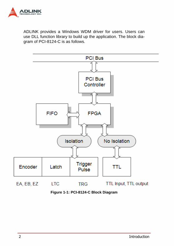
ADLINK provides a Windows WDM driver for users. Users canuse DLL function library to build up the application. The block dia-gram of PCI-8124-C is as follows.
Figure 1-1: PCI-8124-C Block Diagram
Introduction 3
1.1 Features PCI Rev 2.2, 32-bit/33Mhz Compliment
Support both PCI-X (3.3V) and PCI (5V) slots
Support 4-bit board ID for multiple boards in one system
4 differential quardrature encoder counter input channels
Each encoder counter input pair supports 1/2/4x A/B phase, dual pulse (CW/CCW) and signed pulse (OUT/DIR) modes
Internal digital filter
4 trigger output channels via both open collector and TTL pins
Trigger pulse width is software programmable from 0.1µs to 3.2765ms
Each trigger output channel is selected from all comparators, man-ual trigger commands, EZ signal and timers by demands
4 trigger counters that can observe the accuracy of the trigger out-put pulse quantity
4 comparators for comparing encoder counter and FIFO data
10 comparators for comparing encoder counter and linear data
Each encoder counter source is selected from encoder input pins or timers
Comparator data is updated by next FIFO data or linear data when encoder counter is compared and trigger is outputted
14 comparators can select one of 4 trigger output channels individ-ually
4 channel TTL output pins for general purpose output or trigger output
4 channel TTL input pins for general purpose or timer start signal
4 channel high speed latch input pins for counters
EZ and Latch input pins can be used for general purpose input
Latch input logic is selectable by rising or falling edge
Encoder counter clear via EZ input pin as zero operation
Programmable interrupt sources from linear data finished, trig-gered, FIFO empty/full/low, latched, TTL input on.
Switch setting for trigger output default level while power on
Trigger output pin logic programmable
Provide DLL and driver to support Windows 2K/XP/Vista
4 Introduction
1.2 Specifications
Main Chip
Chip Vendor: ACTEL
Model No: A3P1000
Power usage: 3.3V and 1.5V
Reference clock: 40Mhz
Encoder Counters:
Number of channels: 4
Type of wiring: dual differential pairs or single-ended pair
Input Isolated photo coupler: PS9115
Isolated Voltage: 2500 Vrms
Maximum input frequency: 20 MHz (under 4xAB mode)
Supported modes: AB phase x1/2/4, CW/CCW, OUT/DIR
Data length: 32-bit
Digital filter: Yes
Zero Operation: EZ input
Counter Comparators:
Number of comparators: 14
Data length: 32-bit
Trigger pulse width: 0.1µs to 3.2765ms programmable
Internal Timers:
Number of timers: 4
Timer base: 400ns
Resolution: 14-bit
Synchronous start signal: TTL input or register setting
Synchronous stop signal: register setting
Introduction 5
Trigger Output:
Number of channels: 4
Maximum output frequency: 5Mhz
Output types: Open collector or TTL
Open collector Isolated photo-coupler: PS9115
Open collector Isolated: 2500 Vrms
Continuous triggering method: Timer, FIFO or Linear func-tion data reloading
Interrupt: Yes, when triggered
Trigger counter: Yes
Comparator FIFO:
Number of FIFO: 4
FIFO depth: 1023x32bits
Interrupt type: Empty/full/low (1/4,1/2,3/4)
Auto reload: Yes, auto reload next FIFO data to comparator when compared
Comparator Linear Function
Number of Linear Functions: 10
Start Address length: 32-bits
Repeat times length: 32-bit
Interval length: 13-bit
Direction length: 1-bit
Interrupt: Yes, when repeat times count to 0
Auto reload: Yes, auto reload next linear data to comparator when compared
Latch Input
Number of Latch Input pins: 4
Input isolated photo-coupler: PS9115
Isolated Voltage: 2500 Vrms
Band width: 10Mhz
Interrupt: Yes, when latched
6 Introduction
TTL Input
Number of input pins: 4
Photo-coupler Isolated: No
TTL input mode: General purpose or timer synchronous start signal
TTL output
Number of output pins: 4
Photo-coupler Isolated: No
TTL output mode: General purpose output or trigger output
General Specifications
Connectors: 50-pin SCSI-type connector
Operating Temperature: 0C - 70C Storage Temperature: -20C - 80C
Humidity: 5 - 85%, non-condensing
Power Consumption
Slot power supply (input): +5V DC 5%, 450mA(max)
Slot power supply (input): +12V DC 5%, 100mA(max)
Isolation power is from PCI bus (+12V to isolated +5V DC)
PCB Dimension: 151mm(L) X 107mm(W)
Introduction 7
1.3 Supported Software
1.3.1 Programming Library
ADLINK provides Windows WDM driver and DLL function libraryfor the PCI-8124-C. These function libraries are shipped with theboard. It supports for Windows 2000/XP/Vista.

8 Introduction
Installation 9
2 InstallationThis chapter describes how to install the PCI-8124-C. Please fol-low these steps below:
Check what you have (Section 2.1)
Check the PCB (Section 2.2)
Install the hardware (Section 2.3)
Install the software driver (Section 2.4)
Understanding the I/O signal connections (Chapter 3) and their operation (Chapter 4)
2.1 Package Contents
Except this User’s Guide, the package also includes the followingitems:
PCI-8124-C: 4 channel encoder compare trigger board
ADLINK All-in-one Compact Disc
If any of these items are missing or damaged, contact the dealerfrom whom you purchased the product. Save the shipping materi-als and carton to ship or store the product in the future.
10 Installation
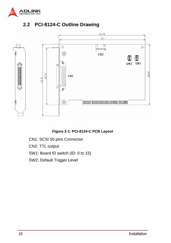
2.2 PCI-8124-C Outline Drawing
Figure 2-1: PCI-8124-C PCB Layout
CN1: SCSI 50 pins Connector
CN2: TTL output
SW1: Board ID switch (ID: 0 to 15)
SW2: Default Trigger Level
Installation 11
2.3 PCI-8124-C Hardware Installation
2.3.1 Hardware Configuration
The PCI-8124-C is fully Plug and Play compliant. Hence memoryallocation (I/O port locations) and IRQ channel of the PCI card areassigned by the system BIOS. The address assignment is doneon a board-by-board basis for all PCI cards in the system.
2.3.2 PCI Slot Selection
Your computer system may have both PCI and ISA slots. Do notforce the PCI card into a PC/AT slot. The PCI-8124-C can be usedin any PCI slot. It also supports dual voltage PCI bus.
2.3.3 Installation Procedures
1. Read through this manual and setup the board indexwith SMD switch. The ID range is from 0 to 15.
2. Turn off your computer. Turn off all accessories (printer,modem, monitor, etc.) connected to computer. Removethe cover from your computer.
3. Select a 32-bit PCI expansion slot. PCI slots are shorterthan ISA or EISA slots and are usually white or ivory.
4. Before handling the PCI-8124-C, discharge any staticbuildup on your body by touching the metal case of thecomputer. Hold the edge of the card and do not touchthe components.
5. Position the board into the PCI slot you have selected.
6. Secure the card in place at the rear panel of the systemunit using screws removed from the slot.
2.3.4 Troubleshooting:
If your system doesn’t boot or if you experience erratic operationwith your PCI board in place, it’s most likely caused by an interruptconflict (possibly an incorrect ISA setup). In general, the solution,once determined it is not a simple oversight, is to consult the BIOSdocumentation that comes with your system.
12 Installation
Check the control panel of the Windows system if the card is listedby the system. If not, check the PCI settings in the BIOS or useanother PCI slot.
2.4 Software Driver Installation
Using the All-In-One CD with PCI-8124-C package and executethe following steps:
1. Autorun the ADLINK All-In-One CD.
2. Follow the procedures of the installer.
3. After setup installation is completed, restart windows.
Installation 13
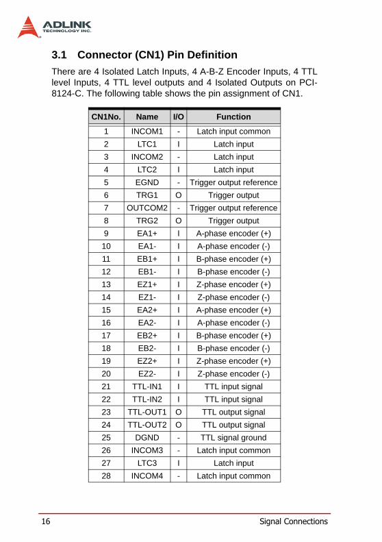
2.5 CN1 Pin Assignments
CN1 is the 50-pin SCSI type connector for I/O signals.
No. Name I/O Function No. Name I/O Function
1 INCOM1 - Latch input common 26 INCOM3 - Latch input common
2 LTC1 I Latch input 27 LTC3 I Latch input
3 INCOM2 - Latch input 28 INCOM4 - Latch input common
4 LTC2 I Latch input 29 LTC4 I Latch input
5 EGND - Trigger output common 30 EGND - Latch input common
6 TRG1 O Trigger output 1 31 TRG3 O Trigger output 3
7 EGND - Trigger output common 32 EGND - Trigger output common
8 TRG2 O Trigger output 2 33 TRG4 O Trigger output 4
9 EA1+ I A-phase encoder (+) 34 EA3+ I A-phase encoder (+)
10 EA1- I A-phase encoder (-) 35 EA3- I A-phase encoder (-)
11 EB1+ I B-phase encoder (+) 36 EB3+ I B-phase encoder (+)
12 EB1- I B-phase encoder (-) 37 EB3- I B-phase encoder (-)
13 EZ1+ I Z-phase encoder (+) 38 EZ3+ I Z-phase encoder (+)
14 EZ1- I Z-phase encoder (-) 39 EZ3- I Z-phase encoder (-)
15 EA2+ I A-phase encoder (+) 40 EA4+ I A-phase encoder (+)
16 EA2- I A-phase encoder (-) 41 EA4- I A-phase encoder (-)
17 EB2+ I B-phase encoder (+) 42 EB4+ I B-phase encoder (+)
18 EB2- I B-phase encoder (-) 43 EB4- I B-phase encoder (-)
19 EZ2+ I Z-phase encoder (+) 44 EZ4+ I Z-phase encoder (+)
20 EZ2- I Z-phase encoder (-) 45 EZ4- I Z-phase encoder (-)
21 TTL-IN1 I TTL input signal 46 TTL-IN3 I TTL input signal
22 TTL-IN2 I TTL input signal 47 TTL-IN4 I TTL input signal
23 TTL-OUT1 O TTL output signal 48 TTL-OUT3 O TTL output signal
24 TTL-OUT2 O TTL output signal 49 TTL-OUT4 O TTL output signal
25 DGND - TTL signal ground 50 DGND - TTL signal ground
Table 2-1: CN1 Pin Assignments
14 Installation
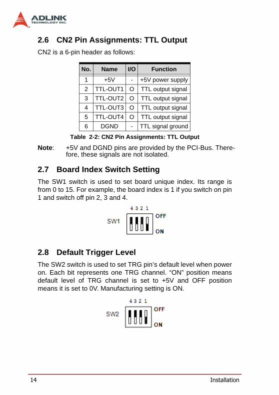
2.6 CN2 Pin Assignments: TTL Output
CN2 is a 6-pin header as follows:
Note: +5V and DGND pins are provided by the PCI-Bus. There-fore, these signals are not isolated.
2.7 Board Index Switch Setting
The SW1 switch is used to set board unique index. Its range isfrom 0 to 15. For example, the board index is 1 if you switch on pin1 and switch off pin 2, 3 and 4.
2.8 Default Trigger Level
The SW2 switch is used to set TRG pin’s default level when poweron. Each bit represents one TRG channel. “ON” position meansdefault level of TRG channel is set to +5V and OFF positionmeans it is set to 0V. Manufacturing setting is ON.
No. Name I/O Function
1 +5V - +5V power supply
2 TTL-OUT1 O TTL output signal
3 TTL-OUT2 O TTL output signal
4 TTL-OUT3 O TTL output signal
5 TTL-OUT4 O TTL output signal
6 DGND - TTL signal ground
Table 2-2: CN2 Pin Assignments: TTL Output
Signal Connections 15
3 Signal ConnectionsSignal connections of all I/O’s are described in this chapter. Referto the contents of this chapter before wiring any cables betweenthe PCI-8124-C and the end device.
This chapter contains the following sections:
Section 3.1 Connector (CN1) Pin Definition
Section 3.2 Isolated Input Ports (LTC, INCOM)
Section 3.3 Isolated Encoder Differential Input
Section 3.4 Isolated Output Ports (TRG, EGND)
Section 3.5 TTL Input Ports
Section 3.6 TTL Output Ports
16 Signal Connections
3.1 Connector (CN1) Pin Definition
There are 4 Isolated Latch Inputs, 4 A-B-Z Encoder Inputs, 4 TTLlevel Inputs, 4 TTL level outputs and 4 Isolated Outputs on PCI-8124-C. The following table shows the pin assignment of CN1.
CN1No. Name I/O Function
1 INCOM1 - Latch input common
2 LTC1 I Latch input
3 INCOM2 - Latch input
4 LTC2 I Latch input
5 EGND - Trigger output reference
6 TRG1 O Trigger output
7 OUTCOM2 - Trigger output reference
8 TRG2 O Trigger output
9 EA1+ I A-phase encoder (+)
10 EA1- I A-phase encoder (-)
11 EB1+ I B-phase encoder (+)
12 EB1- I B-phase encoder (-)
13 EZ1+ I Z-phase encoder (+)
14 EZ1- I Z-phase encoder (-)
15 EA2+ I A-phase encoder (+)
16 EA2- I A-phase encoder (-)
17 EB2+ I B-phase encoder (+)
18 EB2- I B-phase encoder (-)
19 EZ2+ I Z-phase encoder (+)
20 EZ2- I Z-phase encoder (-)
21 TTL-IN1 I TTL input signal
22 TTL-IN2 I TTL input signal
23 TTL-OUT1 O TTL output signal
24 TTL-OUT2 O TTL output signal
25 DGND - TTL signal ground
26 INCOM3 - Latch input common
27 LTC3 I Latch input
28 INCOM4 - Latch input common
Signal Connections 17
29 LTC4 I Latch input
30 EGND - Latch input reference
31 TRG3 O Trigger output
32 EGND - Trigger output reference
33 TRG4 O Trigger output
34 EA3+ I A-phase encoder (+)
35 EA3- I A-phase encoder (-)
36 EB3+ I B-phase encoder (+)
37 EB3- I B-phase encoder (-)
38 EZ3+ I Z-phase encoder (+)
39 EZ3- I Z-phase encoder (-)
40 EA4+ I A-phase encoder (+)
41 EA4- I A-phase encoder (-)
42 EB4+ I B-phase encoder (+)
43 EB4- I B-phase encoder (-)
44 EZ4+ I Z-phase encoder (+)
45 EZ4- I Z-phase encoder (-)
46 TTL-IN3 I TTL input signal
47 TTL-IN4 I TTL input signal
48 TTL-OUT3 O TTL output signal
49 TTL-OUT4 O TTL output signal
50 DGND - TTL signal ground
CN1No. Name I/O Function
18 Signal Connections
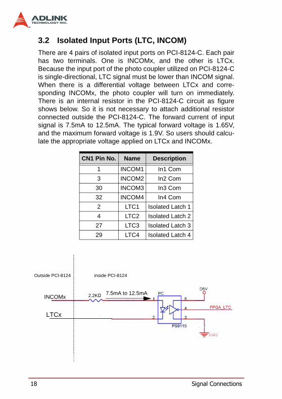
3.2 Isolated Input Ports (LTC, INCOM)
There are 4 pairs of isolated input ports on PCI-8124-C. Each pairhas two terminals. One is INCOMx, and the other is LTCx.Because the input port of the photo coupler utilized on PCI-8124-Cis single-directional, LTC signal must be lower than INCOM signal.When there is a differential voltage between LTCx and corre-sponding INCOMx, the photo coupler will turn on immediately.There is an internal resistor in the PCI-8124-C circuit as figureshows below. So it is not necessary to attach additional resistorconnected outside the PCI-8124-C. The forward current of inputsignal is 7.5mA to 12.5mA. The typical forward voltage is 1.65V,and the maximum forward voltage is 1.9V. So users should calcu-late the appropriate voltage applied on LTCx and INCOMx.
CN1 Pin No. Name Description
1 INCOM1 In1 Com
3 INCOM2 In2 Com
30 INCOM3 In3 Com
32 INCOM4 In4 Com
2 LTC1 Isolated Latch 1
4 LTC2 Isolated Latch 2
27 LTC3 Isolated Latch 3
29 LTC4 Isolated Latch 4
INCOMx
LTCx
Outside PCI-8124 inside PCI-8124
Max 30mA2.2KΩ 7.5mA to 12.5mA
Signal Connections 19
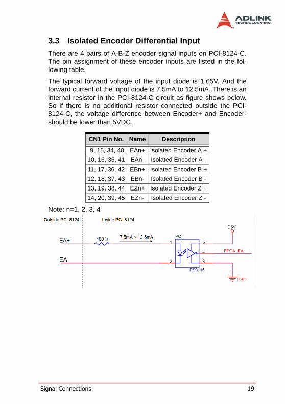
3.3 Isolated Encoder Differential Input
There are 4 pairs of A-B-Z encoder signal inputs on PCI-8124-C.The pin assignment of these encoder inputs are listed in the fol-lowing table.
The typical forward voltage of the input diode is 1.65V. And theforward current of the input diode is 7.5mA to 12.5mA. There is aninternal resistor in the PCI-8124-C circuit as figure shows below.So if there is no additional resistor connected outside the PCI-8124-C, the voltage difference between Encoder+ and Encoder-should be lower than 5VDC.
Note: n=1, 2, 3, 4
CN1 Pin No. Name Description
9, 15, 34, 40 EAn+ Isolated Encoder A +
10, 16, 35, 41 EAn- Isolated Encoder A -
11, 17, 36, 42 EBn+ Isolated Encoder B +
12, 18, 37, 43 EBn- Isolated Encoder B -
13, 19, 38, 44 EZn+ Isolated Encoder Z +
14, 20, 39, 45 EZn- Isolated Encoder Z -
20 Signal Connections
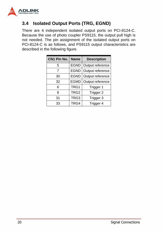
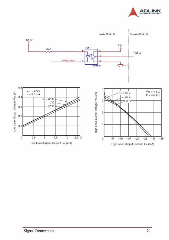
3.4 Isolated Output Ports (TRG, EGND)
There are 4 independent isolated output ports on PCI-8124-C.Because the use of photo coupler PS9115, the output pull high isnot needed. The pin assignment of the isolated output ports onPCI-8124-C is as follows, and PS9115 output characteristics aredescribed in the following figure.
CN1 Pin No. Name Description
5 EGND Output reference
7 EGND Output reference
30 EGND Output reference
32 EGMD Output reference
6 TRG1 Trigger 1
8 TRG2 Trigger 2
31 TRG3 Trigger 3
33 TRG4 Trigger 4
Signal Connections 21
Outside PCI-8124inside PCI-8124
TRGx220Ω
22 Signal Connections
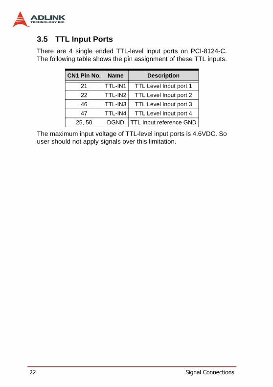
3.5 TTL Input Ports
There are 4 single ended TTL-level input ports on PCI-8124-C.The following table shows the pin assignment of these TTL inputs.
The maximum input voltage of TTL-level input ports is 4.6VDC. Souser should not apply signals over this limitation.
CN1 Pin No. Name Description
21 TTL-IN1 TTL Level Input port 1
22 TTL-IN2 TTL Level Input port 2
46 TTL-IN3 TTL Level Input port 3
47 TTL-IN4 TTL Level Input port 4
25, 50 DGND TTL Input reference GND
Signal Connections 23
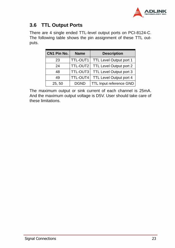
3.6 TTL Output Ports
There are 4 single ended TTL-level output ports on PCI-8124-C.The following table shows the pin assignment of these TTL out-puts.
The maximum output or sink current of each channel is 25mA.And the maximum output voltage is D5V. User should take care ofthese limitations.
CN1 Pin No. Name Description
23 TTL-OUT1 TTL Level Output port 1
24 TTL-OUT2 TTL Level Output port 2
48 TTL-OUT3 TTL Level Output port 3
49 TTL-OUT4 TTL Level Output port 4
25, 50 DGND TTL Input reference GND

24 Signal Connections
Operation Theory 25
4 Operation TheoryThis chapter describes the detail operation of the PCI-8124-Cboard. Contents of the following sections are as follows:
Section 4.1: The trigger board overview
Section 4.2: Trigger board operation
Section 4.3: Multiple boards operation
Section 4.4: Interrupt Control
26 Operation Theory
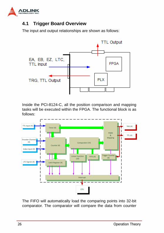
4.1 Trigger Board Overview
The input and output relationships are shown as follows:
Inside the PCI-8124-C, all the position comparison and mappingtasks will be executed within the FPGA. The functional block is asfollows:
The FIFO will automatically load the comparing points into 32-bitcomparator. The comparator will compare the data from counter
Timer (4)
Counter (4)
Latch Register (4)
Comparator (14)
Linear Function (10)
FIFO (4)
PWM&
Mapping
TTL Input (4)
Encoder Channel (4)
Index Input (4)
LTC Signals (4)
TRG (4)
TTL (4)
Interrupt
CPU
Trigger Counter (4)
Operation Theory 27
and FIFO individually. Due to the mapping mechanism, severalcombinations are provided for users to continuously send out thetrigger pulse with isolation or non-isolation channels. Latch signalcan let users retain and retrieve the position data at very shorttime.
Linear function will automatically load the next comparing pointswith a fixed incremental value into 32-bit comparator. Just likeFIFO’s purpose, the new comparing points will be loaded once theprevious comparing point is compared and pulse is triggered.
28 Operation Theory
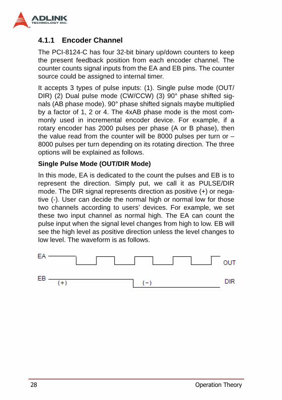
4.1.1 Encoder Channel
The PCI-8124-C has four 32-bit binary up/down counters to keepthe present feedback position from each encoder channel. Thecounter counts signal inputs from the EA and EB pins. The countersource could be assigned to internal timer.
It accepts 3 types of pulse inputs: (1). Single pulse mode (OUT/DIR) (2) Dual pulse mode (CW/CCW) (3) 90° phase shifted sig-nals (AB phase mode). 90° phase shifted signals maybe multipliedby a factor of 1, 2 or 4. The 4xAB phase mode is the most com-monly used in incremental encoder device. For example, if arotary encoder has 2000 pulses per phase (A or B phase), thenthe value read from the counter will be 8000 pulses per turn or –8000 pulses per turn depending on its rotating direction. The threeoptions will be explained as follows.
Single Pulse Mode (OUT/DIR Mode)
In this mode, EA is dedicated to the count the pulses and EB is torepresent the direction. Simply put, we call it as PULSE/DIRmode. The DIR signal represents direction as positive (+) or nega-tive (-). User can decide the normal high or normal low for thosetwo channels according to users’ devices. For example, we setthese two input channel as normal high. The EA can count thepulse input when the signal level changes from high to low. EB willsee the high level as positive direction unless the level changes tolow level. The waveform is as follows.
Operation Theory 29
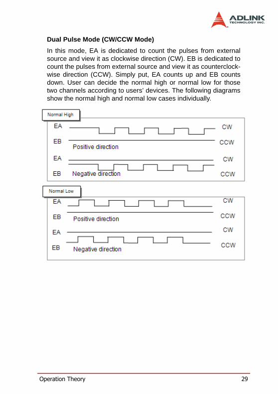
Dual Pulse Mode (CW/CCW Mode)
In this mode, EA is dedicated to count the pulses from externalsource and view it as clockwise direction (CW). EB is dedicated tocount the pulses from external source and view it as counterclock-wise direction (CCW). Simply put, EA counts up and EB countsdown. User can decide the normal high or normal low for thosetwo channels according to users’ devices. The following diagramsshow the normal high and normal low cases individually.
30 Operation Theory
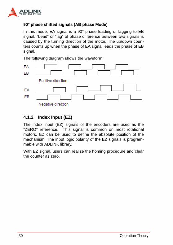
90° phase shifted signals (AB phase Mode)
In this mode, EA signal is a 90° phase leading or lagging to EBsignal. “Lead” or “lag” of phase difference between two signals iscaused by the turning direction of the motor. The up/down coun-ters counts up when the phase of EA signal leads the phase of EBsignal.
The following diagram shows the waveform.
4.1.2 Index Input (EZ)
The index input (EZ) signals of the encoders are used as the“ZERO” reference. This signal is common on most rotationalmotors. EZ can be used to define the absolute position of themechanism. The input logic polarity of the EZ signals is program-mable with ADLINK library.
With EZ signal, users can realize the homing procedure and clearthe counter as zero.
Operation Theory 31
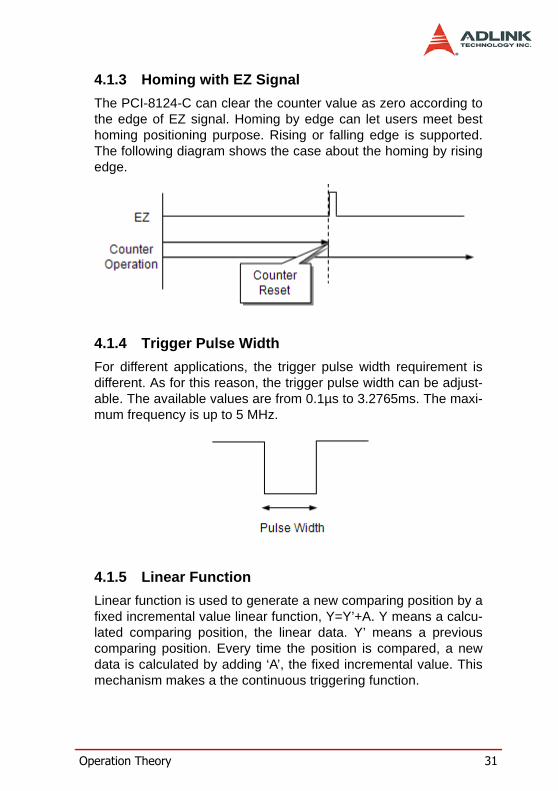
4.1.3 Homing with EZ Signal
The PCI-8124-C can clear the counter value as zero according tothe edge of EZ signal. Homing by edge can let users meet besthoming positioning purpose. Rising or falling edge is supported.The following diagram shows the case about the homing by risingedge.
4.1.4 Trigger Pulse Width
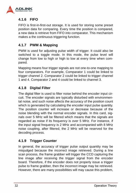
For different applications, the trigger pulse width requirement isdifferent. As for this reason, the trigger pulse width can be adjust-able. The available values are from 0.1µs to 3.2765ms. The maxi-mum frequency is up to 5 MHz.
4.1.5 Linear Function
Linear function is used to generate a new comparing position by afixed incremental value linear function, Y=Y’+A. Y means a calcu-lated comparing position, the linear data. Y’ means a previouscomparing position. Every time the position is compared, a newdata is calculated by adding ‘A’, the fixed incremental value. Thismechanism makes a the continuous triggering function.
32 Operation Theory
4.1.6 FIFO
FIFO is first-in-first-out storage. It is used for storing some presetposition data for comparing. Every time the position is compared,a new data is retrieve from FIFO into comparator. This mechanismmakes a the continuous triggering function.
4.1.7 PWM & Mapping
PWM is used for adjusting pulse width of trigger. It could also beswitched to a toggle mode. In this mode, the pulse level willchange from low to high or high to low at every time when com-pared.
Mapping means four trigger signals are not one-to-one mapping tofour comparators. For example, Comparator 1 could be linked totrigger channel 2. Comparator 2 could be linked to trigger channel1 and 4. Comparator 2 and 4 could be linked to channel 3.
4.1.8 Digital Filter
The digital filter is used to filter noise behind the encoder input cir-cuit. The encoder signals are typically disturbed with environmen-tal noise, and such noise affects the accuracy of the position countwhich is generated by calculating the encoder input pulse quantity.The position counter will increase or decrease because of thenoise blending with the normal encoder signals. In this card, sig-nals over 5 MHz will be filtered which means that the signals areregarded as noise if its frequency is over 5 MHz. For instance, ifthe input signal frequency is 2 MHz and accompanied with 8 MHznoise coupling, after filtered, the 2 MHz will be reserved for thedecoding process.
4.1.9 Trigger Counter
In general, the accuracy of trigger pulse output quantity may bemisjudged because the incorrect image retrieved. During a linescan process, the frame grabber will trigger the CCD capturing theline image after receiving the trigger signal from the encoderboard. Therefore, if the encoder does not properly issue a triggerpulse to frame grabber, then the incorrect image may be retrieved.However, there are many possibilities will may cause this problem,

Operation Theory 33
such as a missing encoder signal, a cable becoming discon-nected, abnormal trigger levels, etc. One method to reduce main-tenance time is by direct observation of the trigger output pulsequantity from the embedded trigger counter inside the on-boardFPGA.
34 Operation Theory
4.2 Trigger Board Operation
This section describes the operation theory for users to knowmore about PCI-8124-C.
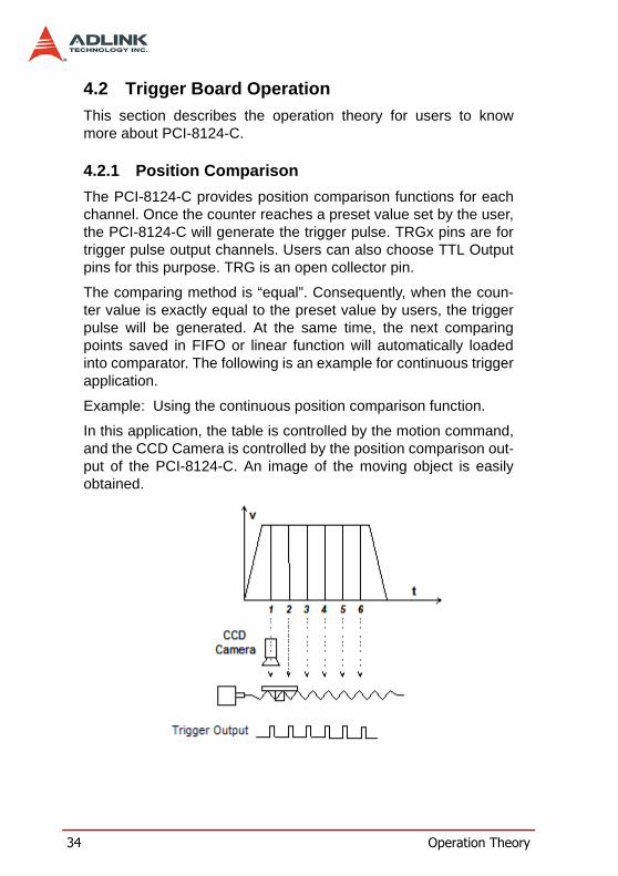
4.2.1 Position Comparison
The PCI-8124-C provides position comparison functions for eachchannel. Once the counter reaches a preset value set by the user,the PCI-8124-C will generate the trigger pulse. TRGx pins are fortrigger pulse output channels. Users can also choose TTL Outputpins for this purpose. TRG is an open collector pin.
The comparing method is “equal”. Consequently, when the coun-ter value is exactly equal to the preset value by users, the triggerpulse will be generated. At the same time, the next comparingpoints saved in FIFO or linear function will automatically loadedinto comparator. The following is an example for continuous triggerapplication.
Example: Using the continuous position comparison function.
In this application, the table is controlled by the motion command,and the CCD Camera is controlled by the position comparison out-put of the PCI-8124-C. An image of the moving object is easilyobtained.
Operation Theory 35
4.2.2 Position Latch
The position latch function is fulfilled by LTC signal. Once the LTCsignal is active, the counter value of its latch channel will be savedto latched register at the same time. User’s can read the latch reg-ister any time.
4.2.3 Linear Function
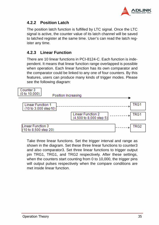
There are 10 linear functions in PCI-8124-C. Each function is inde-pendent. It means that linear function range overlapped is possiblewhen operation. Each linear function has its own comparator andthe comparator could be linked to any one of four counters. By thisfeatures, users can produce many kinds of trigger modes. Pleasesee the following diagram:
Take three linear functions. Set the trigger interval and range asshown in the diagram. Set these three linear functions to counter3and also comparator3. Set three linear functions to trigger outputpin TRG1, TRG1, and TRG2 respectively. After these settings,when the counters start counting from 0 to 10,000, the trigger pinswill output pulses respectively when the compare conditions aremet inside linear function.
36 Operation Theory
4.2.4 FIFO Mode
Continuous triggering is fulfilled by linear function and FIFO.These two modes have their own comparators and can be used atthe same time. The FIFO mode is usually used on random com-paring data condition. Users can preset these data into FIFO andperform continuous triggering. Each FIFO has 1023 random com-paring data space. If users have more random data than 1023, tryto polling FIFO empty status or wait interrupt event and refill resetrandom data.
4.2.5 Timer Function
There are 4 timers on PCI-8124-C. The timer is started by TTLinput and the timer can be set to counters to simulate encoderinputs. It can also output to trigger pins directly. The timer isdesigned by a down-counter. Users must set a counter value intotimer for down counting. Once the timer counter reaches zero, thetimer will output a pulse to trigger pin or increase encoder counterby 1. The down counting speed is 400ns and the maximum coun-ter value is 14-bit.
Operation Theory 37
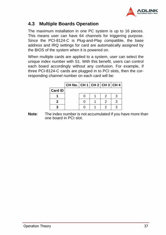
4.3 Multiple Boards Operation
The maximum installation in one PC system is up to 16 pieces.This means user can have 64 channels for triggering purpose.Since the PCI-8124-C is Plug-and-Play compatible, the baseaddress and IRQ settings for card are automatically assigned bythe BIOS of the system when it is powered on.
When multiple cards are applied to a system, user can select theunique index number with S1. With this benefit, users can controleach board accordingly without any confusion. For example, ifthree PCI-8124-C cards are plugged in to PCI slots, then the cor-responding channel number on each card will be:
Note: The index number is not accumulated if you have more than one board in PCI slot.
CH No. CH 1 CH 2 CH 3 CH 4
Card ID
1 0 1 2 3
2 0 1 2 3
3 0 1 2 3
38 Operation Theory
4.4 Interrupt Control
The PCI-8124-C can generate an INT signal to the host PC. Usershave to enable the interrupt service with this function call,_8124_set_int_factor. On the contrary, the parameter of intFactorof function is set to 0 to disable the interrupt service.
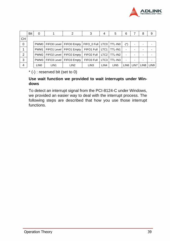
There are 7 kinds of factors could triggered the PCI-8124-C inter-rupt. The factors include:
1. PWM:
When PWM received a comparing trigger include manual trig-ger, it will make an interrupt to host PC.
2. FIFO level:
When the status of FIFO is becoming FIFO level the you set bythe function call “_8124_set_fifo_level”.
3. FIFO empty:
When the FIFO is becoming empty.
4. FIFO full:
When the FIFO is becoming full.
5. LTC:
When the latch counter event is occurred, an interrupt will betriggered.
6. TTL-IN
When timer is triggered by TTL-IN, an interrupt will be gener-ated.
7. Linear function
When linear comparing is finish, it will generate an interrupt.
The following table shows the architecture of interrupt factor ofeach channel. Notice that the INT factors of last channel (ch 4)is not the same with the others. It is used to configure the inter-rupt of linear function.
Operation Theory 39
* (-) : reserved bit (set to 0)
Use wait function we provided to wait interrupts under Win-dows
To detect an interrupt signal from the PCI-8124-C under Windows,we provided an easier way to deal with the interrupt process. Thefollowing steps are described that how you use those interruptfunctions.
Bit 0 1 2 3 4 5 6 7 8 9
CH
0 PWM0 FIFO0 Level FIFO0 Empty FIFO_0 Full LTC0 TTL-IN0 -(*) - - -
1 PWM1 FIFO1 Level FIFO1 Empty FIFO1 Full LTC1 TTL-IN1 - - - -
2 PWM2 FIFO2 Level FIFO2 Empty FIFO2 Full LTC2 TTL-IN2 - - - -
3 PWM3 FIFO3 Level FIFO3 Empty FIFO3 Full LTC3 TTL-IN3 - - - -
4 LIN0 LIN1 LIN2 LIN3 LIN4 LIN5 LIN6 LIN7 LIN8 LIN9
40 Operation Theory
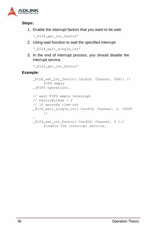
Steps:
1. Enable the interrupt factors that you want to be wait.
“_8124_get_int_factor”
2. Using wait function to wait the specified interrupt.
“_8124_wait_single_int”
3. In the end of interrupt process, you should disable theinterrupt service.
“_8124_get_int_factor”
Example:
_8124_set_int_factor( CardId, Channel, 0x4); // FIFO empty
…(FIFO operation)…
// wait FIFO empty interrupt// FactorBitNum = 2// 10 seconds time-out_8124_wait_single_int( CardId, Channel, 2, 10000
);…_8124_set_int_factor( CardId, Channel, 0 )//
Disable the interrupt service.
TriggerMaster Utility 41
5 TriggerMaster UtilityAfter installing the hardware (Chapters 2 and 3), it is necessary tocorrectly configure all cards and double check the system beforerunning. This chapter gives guidelines for establishing a con-trol system and manually testing the cards to verify correct opera-tion. The TriggerMaster software provides a simple yet powerfulmeans to setup, configure, test, and debug for trigger system, likea line scan system that uses 8124-C cards.
Note that TriggerMaster is only available for Windows 2000/XP/Vista with a screen resolution higher than 1024x768. It cannot beexecuted under a DOS environment.
5.1 Running TriggerMaster
After installing the software drivers for the card in Windows 2000/XP/Vista, the TriggerMaster program can be located at <chosen-path>\PCI-8124-C\TriggerMaster_PCI-8124.exe. To execute theprogram, double click on the executable file or use Start -> Pro-gram Files -> ADLINK -> PCI-8124-C -> TriggerMaster.
5.2 About TriggerMaster
Before running TriggerMaster please note that TriggerMasteris a program written in VB.Net 2003, and is available only forWindows 2000/XP/Vista with a screen resolution higher than1024x768. It cannot be run under DOS.
42 TriggerMaster Utility
5.3 TriggerMaster Form Introduction
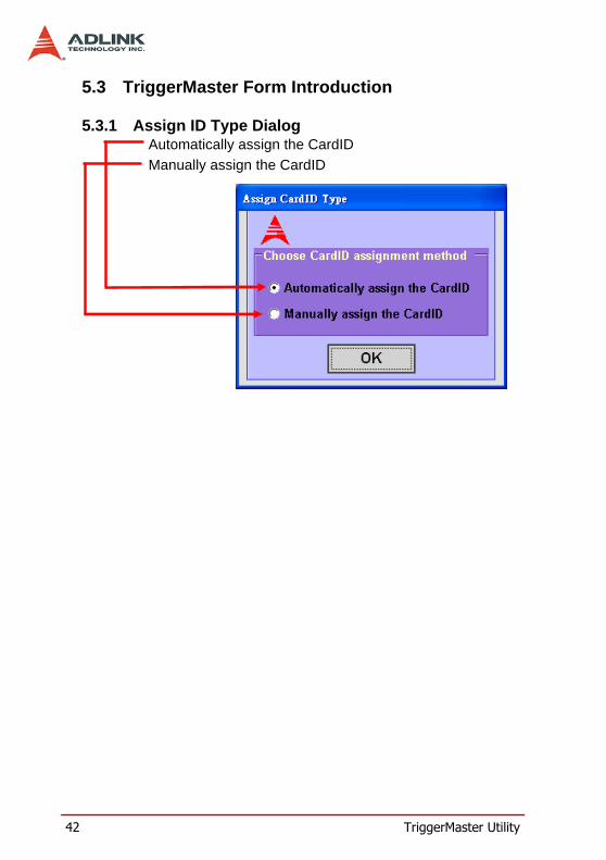
5.3.1 Assign ID Type Dialog
Automatically assign the CardID
Manually assign the CardID
TriggerMaster Utility 43
5.3.2 Main Form
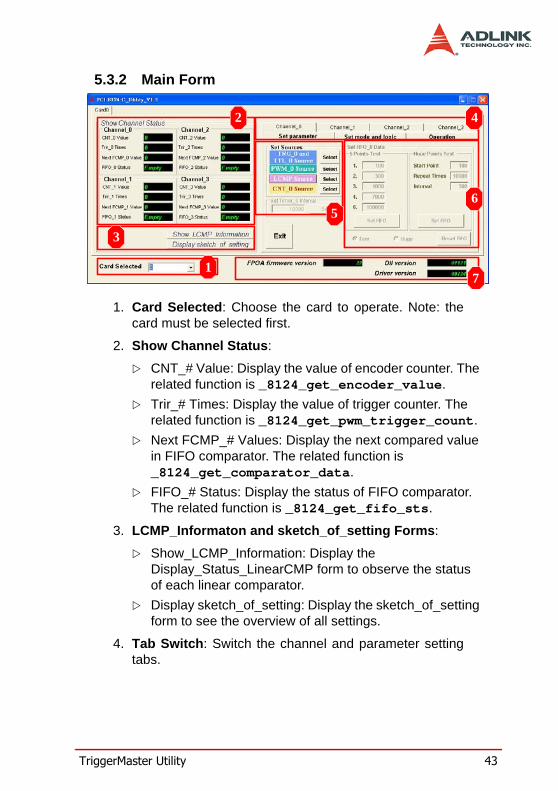
1. Card Selected: Choose the card to operate. Note: thecard must be selected first.
2. Show Channel Status:
CNT_# Value: Display the value of encoder counter. The related function is _8124_get_encoder_value.
Trir_# Times: Display the value of trigger counter. The related function is _8124_get_pwm_trigger_count.
Next FCMP_# Values: Display the next compared value in FIFO comparator. The related function is _8124_get_comparator_data.
FIFO_# Status: Display the status of FIFO comparator. The related function is _8124_get_fifo_sts.
3. LCMP_Informaton and sketch_of_setting Forms:
Show_LCMP_Information: Display the Display_Status_LinearCMP form to observe the status of each linear comparator.
Display sketch_of_setting: Display the sketch_of_setting form to see the overview of all settings.
4. Tab Switch: Switch the channel and parameter settingtabs.
1
3
2 4
56
7
44 TriggerMaster Utility
5. Set Sources:
TRG_# and TTL_# Source: Display the Set_TRG_&_TTL_Out form to set source, logic and mode for TRG output and TTL output for TRG_# and TTL_# output. The related functions are _8124_set_trigger_source, _8124_set_trgOut_logic, and _8124_set_ttlOut_source.
PWM_# Source: Display the Choose_PWM_Source form to set the source for PWM_#. The related function is _8124_set_pwm_source.
LCMP Source: Display the Set_Linear_Comparator form to set each linear comparator. The related functions are _8124_enable_linear_set, _8124_set_linear_compare, and _8124_set_linear_source. Note: the setting in this form is for all channels.
CNT_#: Display the Set_CNT_Source form to set the source for counter_#. The related function is _8124_set_counter_source.
Set_Timer_# Interval: Set the interval timer. The unit is millisecond. The related function is _8124_set_Timer.
6. Set FIFO_# data:
5 Points Test: In this area user can set five data into the FIFO comparator once to verify the functionality of FIFO compare. The related function is _8124_set_fifo_array.
Huge Points Test: In this area user can input a large number of data into the FIFO comparator. The related function is _8124_set_fifo_array ().
Note: if FIFO comparator is not selected the source for the PWM_#, this area is locked.
7. Displays version: Displays the libray, firmware and thedriver version. The related funcion is_8124_get_version.
TriggerMaster Utility 45
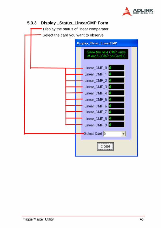
5.3.3 Display _Status_LinearCMP Form
Display the status of linear comparator
Select the card you want to observe
46 TriggerMaster Utility
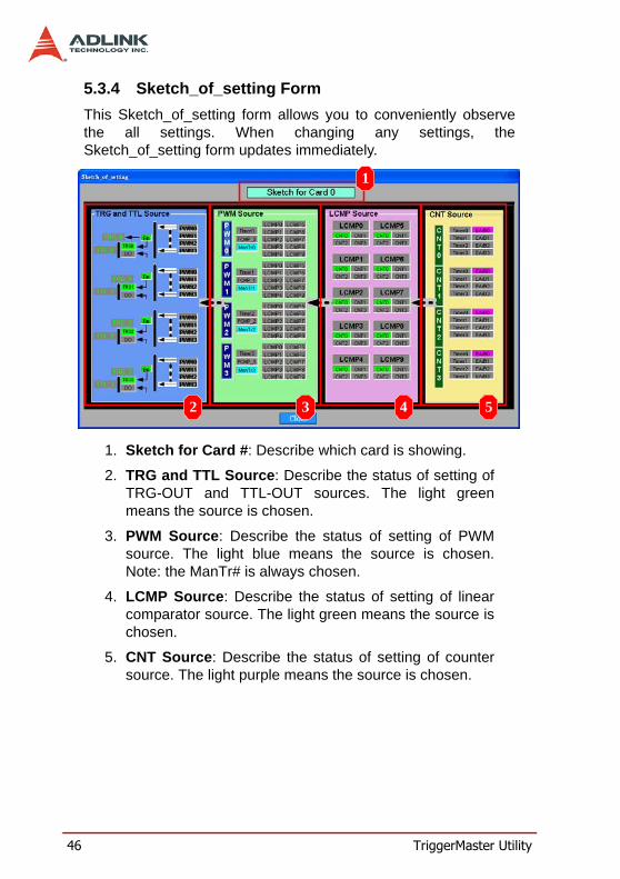
5.3.4 Sketch_of_setting Form
This Sketch_of_setting form allows you to conveniently observethe all settings. When changing any settings, theSketch_of_setting form updates immediately.
1. Sketch for Card #: Describe which card is showing.
2. TRG and TTL Source: Describe the status of setting ofTRG-OUT and TTL-OUT sources. The light greenmeans the source is chosen.
3. PWM Source: Describe the status of setting of PWMsource. The light blue means the source is chosen.Note: the ManTr# is always chosen.
4. LCMP Source: Describe the status of setting of linearcomparator source. The light green means the source ischosen.
5. CNT Source: Describe the status of setting of countersource. The light purple means the source is chosen.
2 3 4 5
1
TriggerMaster Utility 47
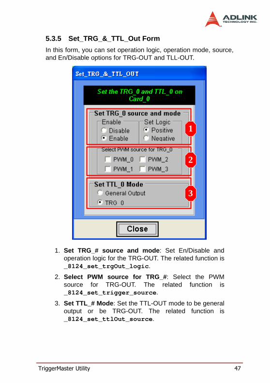
5.3.5 Set_TRG_&_TTL_Out Form
In this form, you can set operation logic, operation mode, source,and En/Disable options for TRG-OUT and TLL-OUT.
1. Set TRG_# source and mode: Set En/Disable andoperation logic for the TRG-OUT. The related function is_8124_set_trgOut_logic.
2. Select PWM source for TRG_#: Select the PWMsource for TRG-OUT. The related function is_8124_set_trigger_source.
3. Set TTL_# Mode: Set the TTL-OUT mode to be generaloutput or be TRG-OUT. The related function is_8124_set_ttlOut_source.
2
3
1
48 TriggerMaster Utility
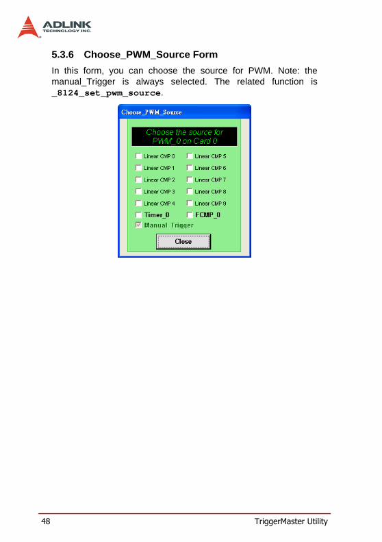
5.3.6 Choose_PWM_Source Form
In this form, you can choose the source for PWM. Note: themanual_Trigger is always selected. The related function is_8124_set_pwm_source.
TriggerMaster Utility 49
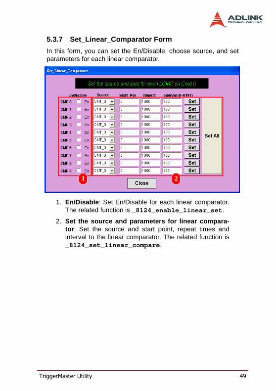
5.3.7 Set_Linear_Comparator Form
In this form, you can set the En/Disable, choose source, and setparameters for each linear comparator.
1. En/Disable: Set En/Disable for each linear comparator.The related function is _8124_enable_linear_set.
2. Set the source and parameters for linear compara-tor: Set the source and start point, repeat times andinterval to the linear comparator. The related function is_8124_set_linear_compare.
1 2
50 TriggerMaster Utility
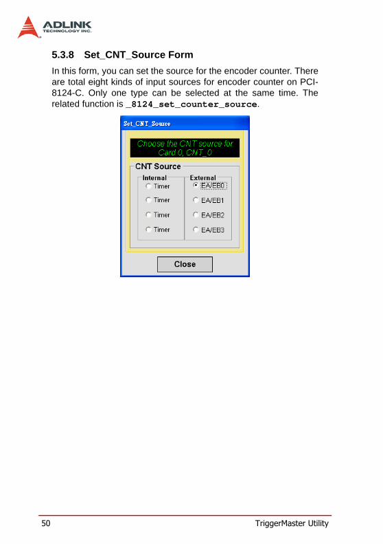
5.3.8 Set_CNT_Source Form
In this form, you can set the source for the encoder counter. Thereare total eight kinds of input sources for encoder counter on PCI-8124-C. Only one type can be selected at the same time. Therelated function is _8124_set_counter_source.
TriggerMaster Utility 51
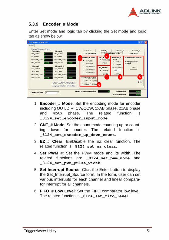
5.3.9 Encoder_# Mode
Enter Set mode and logic tab by clicking the Set mode and logictag as show below:
1. Encoder_# Mode: Set the encoding mode for encoderincluding OUT/DIR, CW/CCW, 1xAB phase, 2xAB phaseand 4xAb phase. The related function is_8124_set_encoder_input_mode.
2. CNT_# Mode: Set the count mode counting up or count-ing down for counter. The related function is_8124_set_encoder_up_down_count.
3. EZ_# Clear: En/Disable the EZ clear function. Therelated function is _8124_set_ez_clear.
4. Set PWM_#: Set the PWM mode and its width. Therelated functions are _8124_set_pwm_mode and_8124_set_pwm_pulse_width.
5. Set Interrupt Source: Click the Enter button to displaythe Set_Interrupt_Source form. In the form, user can setvarious interrupts for each channel and linear compara-tor interrupt for all channels.
6. FIFO_# Low Level: Set the FIFO comparator low level.The related function is _8124_set_fifo_level.
12
3 4 5
6
52 TriggerMaster Utility
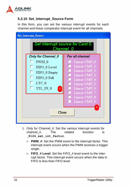
5.3.10 Set_Interrupt_Source Form
In this form, you can set the various interrupt events for eachchannel and linear comparator interrupt event for all channels.
1. Only for Channel_#: Set the various interrupt events forchannel_#. The related function is_8124_set_int_factor.
PWM_#: Set the PWM event to the interrupt factor. This interrupt event occurs when the PWM receives a trigger single.
FIFO_# Level: Set the FIFO_# level event to the inter-rupt factor. This interrupt event occurs when the data in FIFO is less than FIFO level.
1
2
TriggerMaster Utility 53
FIFO_# Empty: Set the FIFO_# empty event to the inter-rupt factor. This interrupt event occurs when the FIFO is empty.
FIFO_# Full: Set the FIFO_# full event to the interrupt factor. This interrupt event occurs when FIFO is full.
LTC_#: Set the LTC_# event to the interrupt factor. This interrupt event occurs when specified latch contition meet.
TTL_IN_#: Set the TTL_IN_# event to the interrupt fac-tor. This interrupt event occurs when TTL_IN_# receives a signal.
2. For all channel: Set the linear comparator event to theinterrupt factor. This interrupt event occurs when thecomparing in linear comparator is finished.
54 TriggerMaster Utility
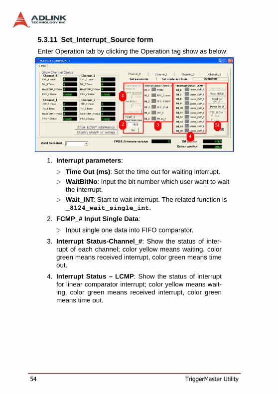
5.3.11 Set_Interrupt_Source form
Enter Operation tab by clicking the Operation tag show as below:
1. Interrupt parameters:
Time Out (ms): Set the time out for waiting interrupt.
WaitBitNo: Input the bit number which user want to wait the interrupt.
Wait_INT: Start to wait interrupt. The related function is _8124_wait_single_int.
2. FCMP_# Input Single Data:
Input single one data into FIFO comparator.
3. Interrupt Status-Channel_#: Show the status of inter-rupt of each channel; color yellow means waiting, colorgreen means received interrupt, color green means timeout.
4. Interrupt Status – LCMP: Show the status of interruptfor linear comparator interrupt; color yellow means wait-ing, color green means received interrupt, color greenmeans time out.
1
2 3
4
51
TriggerMaster Utility 55
5. Buttons:
Start Timer_#: Start the interval timer.
Reset CNT_#: Reset the counter value.
Reset Trir CNT_#: Reset the trigger counter value.
Manual Trir_#: Trigger pulse manually.
TTL_# Out: TTL_out output high or low. If TTL_Out mode is trg-out, it can’t be operated.

56 TriggerMaster Utility
Function Library 57
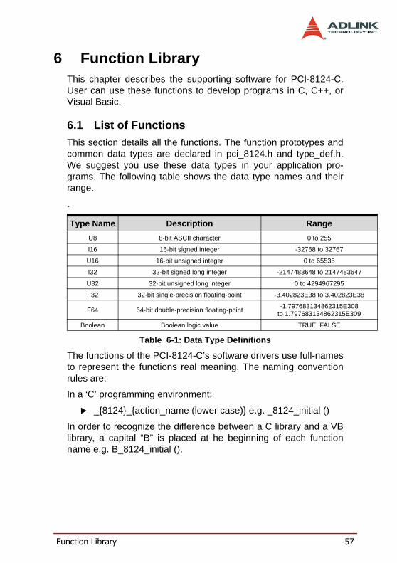
6 Function LibraryThis chapter describes the supporting software for PCI-8124-C.User can use these functions to develop programs in C, C++, orVisual Basic.
6.1 List of Functions
This section details all the functions. The function prototypes andcommon data types are declared in pci_8124.h and type_def.h.We suggest you use these data types in your application pro-grams. The following table shows the data type names and theirrange.
.
Table 6-1: Data Type Definitions
The functions of the PCI-8124-C’s software drivers use full-namesto represent the functions real meaning. The naming conventionrules are:
In a ‘C’ programming environment:
_8124_action_name (lower case) e.g. _8124_initial ()
In order to recognize the difference between a C library and a VBlibrary, a capital “B” is placed at he beginning of each functionname e.g. B_8124_initial ().
Type Name Description Range
U8 8-bit ASCII character 0 to 255
I16 16-bit signed integer -32768 to 32767
U16 16-bit unsigned integer 0 to 65535
I32 32-bit signed long integer -2147483648 to 2147483647
U32 32-bit unsigned long integer 0 to 4294967295
F32 32-bit single-precision floating-point -3.402823E38 to 3.402823E38
F64 64-bit double-precision floating-point-1.797683134862315E308
to 1.797683134862315E309
Boolean Boolean logic value TRUE, FALSE
58 Function Library
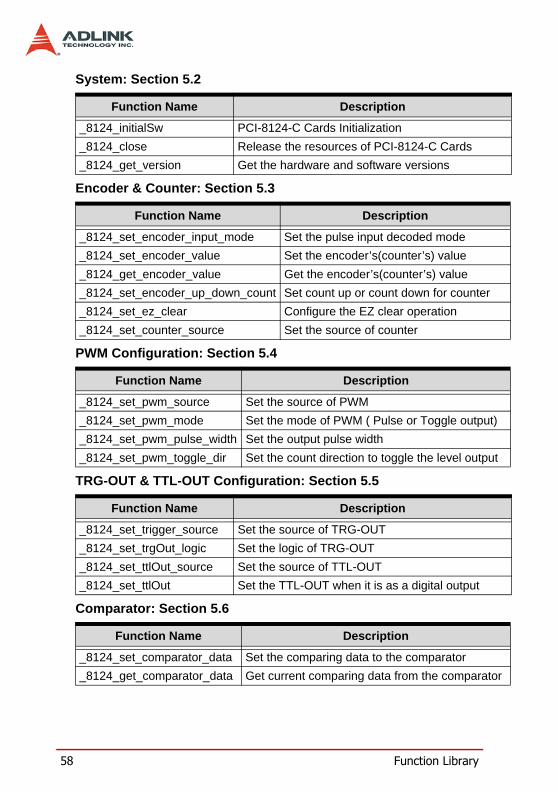
System: Section 5.2
Encoder & Counter: Section 5.3
PWM Configuration: Section 5.4
TRG-OUT & TTL-OUT Configuration: Section 5.5
Comparator: Section 5.6
Function Name Description
_8124_initialSw PCI-8124-C Cards Initialization
_8124_close Release the resources of PCI-8124-C Cards
_8124_get_version Get the hardware and software versions
Function Name Description
_8124_set_encoder_input_mode Set the pulse input decoded mode
_8124_set_encoder_value Set the encoder’s(counter’s) value
_8124_get_encoder_value Get the encoder’s(counter’s) value
_8124_set_encoder_up_down_count Set count up or count down for counter
_8124_set_ez_clear Configure the EZ clear operation
_8124_set_counter_source Set the source of counter
Function Name Description
_8124_set_pwm_source Set the source of PWM
_8124_set_pwm_mode Set the mode of PWM ( Pulse or Toggle output)
_8124_set_pwm_pulse_width Set the output pulse width
_8124_set_pwm_toggle_dir Set the count direction to toggle the level output
Function Name Description
_8124_set_trigger_source Set the source of TRG-OUT
_8124_set_trgOut_logic Set the logic of TRG-OUT
_8124_set_ttlOut_source Set the source of TTL-OUT
_8124_set_ttlOut Set the TTL-OUT when it is as a digital output
Function Name Description
_8124_set_comparator_data Set the comparing data to the comparator
_8124_get_comparator_data Get current comparing data from the comparator
Function Library 59
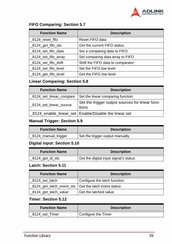
FIFO Comparing: Section 5.7
Linear Comparing: Section 5.8
Manual Trigger: Section 5.9
Digital input: Section 5.10
Latch: Section 5.11
Timer: Section 5.12
Function Name Description
_8124_reset_fifo Reset FIFO data
_8124_get_fifo_sts Get the current FIFO status
_8124_set_fifo_data Set a comparing data to FIFO
_8124_set_fifo_array Set comparing data array to FIFO
_8124_set_fifo_shift Shift the FIFO data to comparator
_8124_set_fifo_level Set the FIFO low level
_8124_get_fifo_level Get the FIFO low level
Function Name Description
_8124_set_linear_compare Set the linear comparing function
_8124_set_linear_sourceSet the trigger output sources for linear func-tions
_8124_enable_linear_set Enable/Disable the linear set
Function Name Description
_8124_manual_trigger Set the trigger output manually
Function Name Description
_8124_get_di_sts Get the digital input signal’s status
Function Name Description
_8124_set_latch Configure the latch function
_8124_get_latch_event_sts Get the latch event status
_8124_get_latch_value Get the latched value
Function Name Description
_8124_set_Timer Configure the Timer
60 Function Library
Interrupt Control: Section 5.13
Filtering & Monitoring: Section 5.14
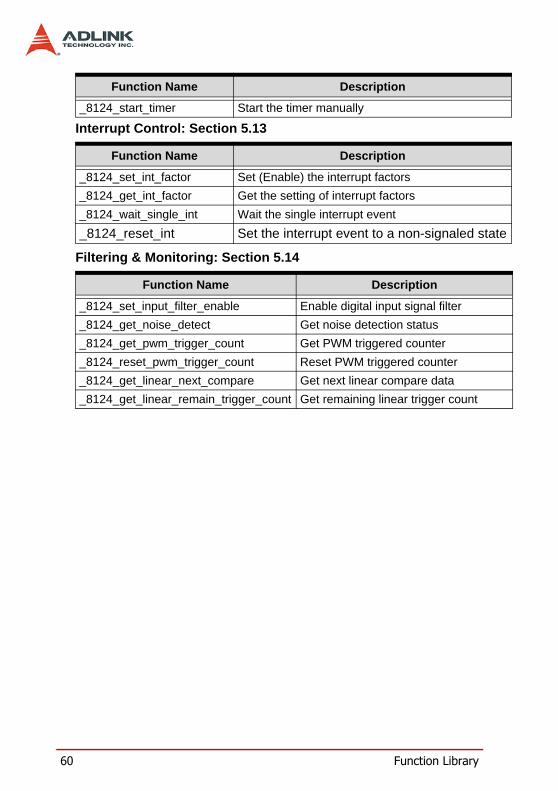
_8124_start_timer Start the timer manually
Function Name Description
_8124_set_int_factor Set (Enable) the interrupt factors
_8124_get_int_factor Get the setting of interrupt factors
_8124_wait_single_int Wait the single interrupt event
_8124_reset_int Set the interrupt event to a non-signaled state
Function Name Description
_8124_set_input_filter_enable Enable digital input signal filter
_8124_get_noise_detect Get noise detection status
_8124_get_pwm_trigger_count Get PWM triggered counter
_8124_reset_pwm_trigger_count Reset PWM triggered counter
_8124_get_linear_next_compare Get next linear compare data
_8124_get_linear_remain_trigger_count Get remaining linear trigger count
Function Name Description
Function Library 61
6.2 System & Initialization
@ Name
@ Description
_8124_initialSw:
This function is used to initialize the PCI-8124-C cards in yoursystem. All PCI-8124-C cards must be initialized by this func-tion before calling other functions. The ID of cards can beassigned by system automatically or dip switch (SW1) manu-ally.
The source of TRG-OUT and TTL-OUT output signals can bedecided by SW2 or PWM output. See also section 5.5“_8124_set_trigger_source”.
If DefaultSw = 1, the output signal of TRG-OUT and TTL-OUTwill output as SW2. On the contrary, if DefaultSw = 0, the TRG-OUT will output as PWM default setting and TTL-OUT will out-put D5V ( as a digital output).
_8124_close:
This function is to close the PCI-8124-C cards and release itsresources, which must be called at the end of your applica-tions.
_8124_get_version:
Users can get the hardware and software version number bythis function.
_8124_initialSw PCI-8124-C Cards Initialization
_8124_closeRelease the resources of PCI-8124-C Cards
_8124_get_version Get the hardware and software versions
62 Function Library
@ Syntax
C/C++ (Windows 2000/XP)I16 _8124_initialSw( I16 *CardIdInBit, I16
ManualId, I16 DefaultSw ); I16 _8124_close();I16 _8124_get_version(I16 CardId, I32
*Firmware_ver, I32 *Driver_ver, I32 *DLL_ver);
Visual Basic (Windows 2000/XP)B_8124_initialSw (CardIdInBit As Integer, ByVal
ManualId As Integer, ByVal DefaultSw As Integer) As Integer
B_8124_close () As IntegerB_8124_get_version (ByVal CardId As Integer,
Firmware_ver As Long, Driver_ver As Long, DLL_ver As Long) As Integer
@ Arguments
I16 *CardIdInBit: The information of PCI-8124-C cards’ cardID in bit format.
Ex. CardIdInBit = 0x0009; It means there are two PCI-8124-C cards in your system
Card_0’s ID = 0, Card_1’s ID = 3
I16 ManualId: Cards’ ID decided by SW1
0: Decided by system,
1:Decided by dip switch(SW1)
I16 DefaultSw: Default output setting.
0: Default output as PWM and Digital out
1: Default output as SW2
I16 CardId: The PCI-8124-C card’s ID number. (0 ~ 15)
I32 *Firmware_ver: The firmware version.
I32 *Driver_ver: The device driver version.
I32 *DLL_ver: The DLL’ version.
Function Library 63
6.3 Encoder & Counter
@ Name
@ Description
_8124_set_encoder_input_mode:
There are 5 types of pulse input mode(EA/EB) including OUT/DIR, CW/CCW, 1x , 2x, and 4x AB phase. Choose a correctencoder input mode before using counter.
_8124_set_encoder_value:
This function is used to set the encoder( counter ) valuedirectly.
_8124_get_encoder_value:
This function is used to read the current encoder value.
_8124_set_encoder_up_down_count:
This function is used to set the specified encoder to count up orcount down.
_8124_set_ez_clear:
This function is used to enable the function of counter clear bysensing EZ input signal. If enabled, you should choose fallingedge or rising edge to clear counter. On the contrary, if dis-abled, the setting of “ClrLogic” will be ignored.
_8124_set_encoder_input_mode Set the pulse input decoded mode
_8124_set_encoder_value Set the encoder’s(counter’s) value
_8124_get_encoder_value Get the encoder’s(counter’s) value
_8124_set_encoder_up_down_count Set count up or count down for counter
_8124_set_ez_clear Configure the EZ clear operation
_8124_set_counter_source Set the source of counter
64 Function Library
_8124_set_counter_source:
This function is used to set the counter source. The sourcecould be one of the EA/EB input channels or timers. Thedefault counter source is EA/EB. About timer, please refer thesection 5.12 Timer.
@ Syntax
C/C++ (Windows 2000/XP)I16 _8124_set_encoder_input_mode( I16 CardId, I16
Channel, I16 IptMode );I16 _8124_set_encoder_value( I16 CardId, I16
Channel, I32 EncValue );I16 _8124_get_encoder_value( I16 CardId, I16
Channel, I32 *EncValue );I16 _8124_set_encoder_up_down_count(I16 CardId,
I16 Channel, I16 Inverse );I16 _8124_set_ez_clear( I16 CardId, I16 Channel,
I16 Enable, I16 ClrLogic );I16 _8124_set_counter_source( I16 CardId, I16
Channel, I16 CtnSrc );
Visual Basic (Windows 2000/XP)B_8124_set_pls_iptmode (ByVal CardId As Integer,
ByVal Channel As Integer, ByVal IptMode As Integer) As Integer
B_8124_set_encoder_input_mode (ByVal CardId As Integer, ByVal Channel As Integer, ByVal IptMode As Integer) As Integer
B_8124_set_encoder_value (ByVal CardId As Integer, ByVal Channel As Integer, ByVal EncValue As Long) As Integer
B_8124_get_encoder_value (ByVal CardId As Integer, ByVal Channel As Integer, EncValue As Long) As Integer
B_8124_set_encoder_up_down_count (ByVal CardId As Integer, ByVal Channel As Integer, ByVal Inverse As Integer) As Integer
B_8124_set_ez_clear (ByVal CardId As Integer, ByVal Channel As Integer, ByVal Enable As Integer, ByVal ClrLogic As Integer) As Integer
Function Library 65
B_8124_set_counter_source (ByVal CardId As Integer, ByVal Channel As Integer, ByVal CtnSrc As Integer) As Integer
@ Argument
I16 CardId: The PCI-8124-C card’s ID number.
I16 Channel: The specified channel number. (0 – 3)
I16 IptMode: The pulse input mode.
0: OUT/DIR (default)
1: CW/CCW
2: 1x AB-Phase
3: 2x AB-Phase
4: 4x AB-Phase
I32 EncValue: The encoder (counter) value.
I16 Inverse: Encoder count direction inverse or not
0: Not inverse (default)
1: Inverse
I16 Enable: Enable EZ-clear function
0: Disable (default)
1: Enable
I16 ClrLogic: Clear logic setting
0: Photo couple: OFF ON (Falling edge) clear (default)
1: Photo couple: ON OFF (Rising edge) clear
I16 CtnSrc: The counter’s source (0 – 7)
0 – 3: EA/EB 0 – 3
4 – 7: Timer 0 – 3
66 Function Library
6.4 PWM Configuration
@ Name
@ Description
_8124_set_pwm_source:
This function is used to set the PWM source (trigger source). APWM has 3 kinds of source, LIN, CMP and timer respectively.Those three kind of sources are independently. Users canenable them at the same time. The default setting is CMP.
_8124_set_pwm_mode:
There are two types of TRG output. One is pulse type output,the other is level-switch output. Users can select output type bythis function.
_8124_set_pwm_pulse_width:
If you selected the pulse type output as the PWM output. Youcan adjust the pulse width by this function.
_8124_set_pwm_toggle_dir:
If you selected the level-switch output as the PWM output, youcan set the toggled condition by this function. There are 3 con-ditions (count directions) that the level output could be toggled.
@ Syntax
C/C++ (Windows 2000/XP)I16 _8124_set_pwm_source( I16 CardId, I16
Channel, I16 CmpEn, I16 LinearEn, I16 TimerEn );
_8124_set_pwm_source Set the source of PWM
_8124_set_pwm_mode Set the mode of PWM ( Pulse or Toggle output)
_8124_set_pwm_pulse_width Set the output pulse width
_8124_set_pwm_toggle_dir Set the count direction to toggle the level output
Function Library 67
I16 _8124_set_pwm_mode( I16 CardId, I16 Channel, I16 PulseOrToggle );
I16 _8124_set_pwm_pulse_width( I16 CardId, I16 Channel, I16 WidthPara );
I16 _8124_set_pwm_toggle_dir( I16 CardId, I16 Channel, I16 ToggleDir );
Visual Basic (Windows 2000/XP)B_8124_set_pwm_source (ByVal CardId As Integer,
ByVal Channel As Integer, ByVal CmpEn As Integer, ByVal LinearEn As Integer, ByVal TimerEn As Integer) As Integer
B_8124_set_pwm_mode (ByVal CardId As Integer, ByVal Channel As Integer, ByVal PulseOrToggle As Integer) As Integer
B_8124_set_pwm_pulse_width (ByVal CardId As Integer, ByVal Channel As Integer, ByVal WidthPara As Integer) As Integer
B_8124_set_pwm_toggle_dir (ByVal CardId As Integer, ByVal Channel As Integer, ByVal ToggleDir As Integer) As Integer
@ Argument
I16 CardId: The PCI-8124-C card’s ID number.
I16 Channel: The channel’s number of PWM
I16 CmpEn: Enable CMP(FIFO comparing) source (0: Disable, 1:Enable)
I16 LinearEn: Enable Linear comparing (0: Disable, 1: Enable)
I16 TimerEn: Enable timer source. (0: Disable, 1:Enable)
I16 PulseOrToggle: Select the pulse output or level switch out-put
0: Pulse output
1: Level switch output (toggle output)
I16 WidthPara: The parameter of pulse width. (0 – 8191)
Pulse width(ns) = ( WidthPara × 16 + 4 ) × 25
68 Function Library
I16 ToggleDir: Toggled condition select
0: Directionless
1: Count up
2: Count down
Function Library 69
6.5 TRG-OUT & TTL-OUT Configuration
@ Name
@ Description
_8124_set_trigger_source:
There are two kinds of TGR sources. One is from SW2 setting,the other is from PWM or DI signals. If you select SW2 setting,the function will ignore the setting of parameters “PwmInBit”,“TtlInInBit” and “EzInBit”. On the contrary, If you select PWM/TTL-IN/EZ as source, you should set the other parameters innext. They can be “OR” output.
_8124_set_trgOut_logic:
This function is used to set the logic of TRG –OUT output sig-nal.
_8124_set_ttlOut_source:
This function is used to set the source of TTL-OUT output.There are two sources of TTL-OUT output. One is DO output.The other is output as the relative channel of TRG-OUT output.
Caution: Because of the logic of TRG-OUT outputs can beinversed, the logic of TRG-OUT output and TTL-OUT out-put may opposite.
_8124_set_ttlOut:
When TTL-OUT is set as digital output (DO), you can control itby this function.
_8124_set_trigger_source Set the source of TRG-OUT
_8124_set_trgOut_logic Set the logic of TRG-OUT
_8124_set_ttlOut_source Set the source of TTL-OUT
_8124_set_ttlOut Set the TTL-OUT when it is as a digital output
70 Function Library
@ Syntax
C/C++ (Windows 2000/XP)I16 _8124_set_trigger_source( I16 CardId, I16
Channel, I16 GroupSel, I16 PwmInBit, I16 TtlInInBit, I16 EzInBit );
I16 _8124_set_ttlOut_source( I16 CardId, I16 Channel, I16 TtlOutSrc );
I16 _8124_set_ttlOut( I16 CardId, I16 Channel, I16 TtlOutValue );
Visual Basic (Windows 2000/XP)B_8124_set_trigger_source (ByVal CardId As
Integer, ByVal Channel As Integer, ByVal GroupSel As Integer, ByVal PwmInBit As Integer, ByVal TtlInInBit As Integer, ByVal EzInBit As Integer) As Integer
B_8124_set_trgOut_logic (ByVal CardId As Integer, ByVal Channel As Integer, ByVal Logic As Integer) As Integer
B_8124_set_ttlOut_source (ByVal CardId As Integer, ByVal Channel As Integer, ByVal TtlOutSrc As Integer) As Integer
B_8124_set_ttlOut (ByVal CardId As Integer, ByVal Channel As Integer, ByVal TtlOutValue As Integer) As Integer
@ Argument
I16 CardId: The PCI-8124-C card’s ID number.
I16 Channel: The channel’s number of TRG-OUT / TTL-OUT.
I16 GroupSel: The TRG-OUT source.
0: Output according to SW2 setting
1: PWM / TTL-IN / EZ signal
I16 PwmInBit: The source of PWM channel in bit format.
Ex: PwmInBit = 0x2, means PWM_1
I16 TtlInInBit: The source of TTL-IN channel in bit format.
Ex: TtlInInBit = 0x6, means TTL-IN1 and TTL-IN_2
Function Library 71
I16 EzInBit: The source of EZ channel in bit format.
Ex: EzInBit = 0x1, means EZ_0
I16 TtlOutSrc: The TTL-OUT output source
0: use as Digital output
1: Follow TRG-OUT
I16 TtlOutValue: TTL-OUT output control
0: DGND.
1: D5V.
72 Function Library
6.6 Comparator
@ Name
@ Description
_8124_set_comparator_data:
This function is used to override the current comparing data tothe comparator (CMP).
_8124_get_comparator_data:
This function is used to get the current comparing data fromcomparator (CMP).
@ Syntax
C/C++ (Windows 2000/XP)I16 _8124_set_comparator_data( I16 CardId, I16
Channel, I32 CmpData );I16 _8124_get_comparator_data( I16 CardId, I16
Channel, I32 *CmpData );Visual Basic (Windows 2000/XP)B_8124_set_comparator_data (ByVal CardId As
Integer, ByVal Channel As Integer, ByVal CmpData As Long) As Integer
B_8124_get_comparator_data (ByVal CardId As Integer, ByVal Channel As Integer, CmpData As Long) As Integer
@ Argument
I16 CardId: The PCI-8124-C card’s ID number.
I16 Channel: The channel’s number of comparator (CMP).
I32 CmpData: The current comparing data in comparator.
_8124_set_comparator_data Set the comparing data to the comparator
_8124_get_comparator_data Get current comparing data from the comparator
Function Library 73
6.7 FIFO Comparing
@ Name
@ Description
_8124_reset_fifo:
This function is used to reset (clear) the FIFO. The FIFO statusis return “Empty” status, when you issue this function.
_8124_get_fifo_sts:
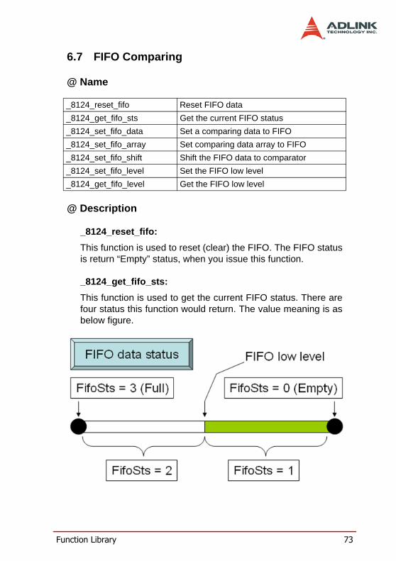
This function is used to get the current FIFO status. There arefour status this function would return. The value meaning is asbelow figure.
_8124_reset_fifo Reset FIFO data
_8124_get_fifo_sts Get the current FIFO status
_8124_set_fifo_data Set a comparing data to FIFO
_8124_set_fifo_array Set comparing data array to FIFO
_8124_set_fifo_shift Shift the FIFO data to comparator
_8124_set_fifo_level Set the FIFO low level
_8124_get_fifo_level Get the FIFO low level
74 Function Library
_8124_set_fifo_data:
This function is used to set the specified comparing data to theFIFO. The capacity of FIFO is 1023. When the status of FIFO isfull, the data cannot be set into FIFO. This function won’t checkthe FIFO status.
_8124_set_fifo_array:
This function is used to set comparing data array to the FIFO.
_8124_set_fifo_shift:
This function is used to shift the FIFO data to comparator(CMP) manually. Generally, when using the FIFO comparing,the first compared data must shift to the CMP manually via thisfunction.
_8124_set_fifo_level:
This function is used to set the FIFO low level. There are fourconditions in FIFO low level selection. The default setting is512 elements remaining in FIFO.
_8124_get_fifo_level:
This function is used to get the setting of FIFO low level.
@ Syntax
C/C++ (Windows 2000/XP)I16 _8124_reset_fifo( I16 CardId, I16 Channel );I16 _8124_get_fifo_sts( I16 CardId, I16 Channel,
I16 *FifoSts );I16 _8124_set_fifo_data( I16 CardId, I16 Channel,
I32 FifoData );I16 _8124_set_fifo_array( I16 CardId, I16
Channel, I32 *DataArr, I16 ArraySize );I16 _8124_set_fifo_shift( I16 CardId, I16 Channel
);I16 _8124_set_fifo_level( I16 CardId, I16
Channel, I16 Level ); I16 _8124_get_fifo_level( I16 CardId, I16
Channel, I16 *Level );
Function Library 75
Visual Basic (Windows 2000/XP)B_8124_reset_fifo (ByVal CardId As Integer, ByVal
Channel As Integer) As IntegerB_8124_get_fifo_sts (ByVal CardId As Integer,
ByVal Channel As Integer, FifoSts As Integer) As Integer
B_8124_set_fifo_data (ByVal CardId As Integer, ByVal Channel As Integer, ByVal FifoData As Long) As Integer
B_8124_set_fifo_array (ByVal CardId As Integer, ByVal Channel As Integer, DataArr As Long, ByVal ArraySize As Integer) As Integer
B_8124_set_fifo_shift (ByVal CardId As Integer, ByVal Channel As Integer) As Integer
B_8124_set_fifo_level (ByVal CardId As Integer, ByVal Channel As Integer, ByVal Level As Integer) As Integer
B_8124_get_fifo_level (ByVal CardId As Integer, ByVal Channel As Integer, Level As Integer) As Integer
@ Argument
I16 CardId: The PCI-8124-C card’s ID number.
I16 Channel: The channel’s number of FIFO ( 0 – 3 )
I16 *FifoSts: The FIFO status.
0: FIFO datas = Empty
1: Low level FIFO data > Empty
2: Full > FIFO data > Low level
3: FIFO = Full
I32 FifoData: The data to FIFO.
I32 *DataArr: The data array to FIFO
I16 ArraySize: The size of data array to FIFO. ( 1 – 1023 )
76 Function Library
I16 Level: The FIFO low level setting.(remaining data numbersin FIFO)
0: Low level = 0 (Empty)
1: Low level = 256 ( 1/4 FIFO size )
2: Low level = 512 ( 1/2 FIFO size ) (Default)
3: Low level = 768 ( 3/4 FIFO size )
Function Library 77
6.8 Linear Comparing
@ Name
@ Description
_8124_set_linear_compare:
This function is used to configure the linear comparing triggerfunction. Before using linear comparing function, you shouldenable the source of PWM from linear function by“_8124_set_pwm_source”. PCI-8124-C has 10 linear sets canbe used for linear and they can be compared with any counterarbitrarily. Every set has 3 parameters including starting point(StartPoint), repeat times (RepeatTimes) and trigger interval(Interval). The total trigger pulse would be (RepeatTimes + 1)times. For example, if you set the RepeatTimes as 10, the totaloutput pulse will be 11. The follow formula is show that how doyou calculate the next triggering position.
Next triggering position = StartPoint + Interval x N
N: triggered times, ( N RepeatTimes)
The Interval can be set as a negative value. The comparingdirection is depending on the signed of Interval. Moreover, ifRepeatTimes is set to 0, the linear comparing will not stop untilstopping counting or reset the linear function.
_8124_set_linear_source:
There are 10 linear sets in PCI-8124-C. Use this function toassign which sets will be used in the specified trigger channel.One trigger channel can have more then one linear set.
_8124_set_linear_compare Set the linear comparing function
_8124_set_linear_sourceSet the trigger output sources for linear functions
_8124_enable_linear_set Enable/Disable the linear set
78 Function Library
_8124_enable_linear_set:
The PCI-8124-C has 10 linear sets. Before using these linearsets, enable the linear set by this function. When linear sets areno longer needed, it is recommended that the the linear set bedisabled, or it could be unexpectedly triggered.
@ Syntax
C/C++ (Windows 2000/XP)I16 _8124_set_linear_compare( I16 CardId, I16
SetNum, I16 Channel, I32 StartPoint, F64 RepeatTimes, I16 Interval );
I16 _8124_set_linear_source( I16 CardId, I16 Channel, I16 SetNumInBit );
I16 _8124_enable_linear_set( I16 CardId, I16 SetNum, I16 Enable );
Visual Basic (Windows 2000/XP)B_8124_set_linear_compare (ByVal CardId As
Integer, ByVal SetNum As Integer, ByVal Channel As Integer, ByVal StartPoint As Long, ByVal RepeatTimes As Double, ByVal Interval As Integer) As Integer
B_8124_set_linear_source( ByVal CardId As Integer, ByVal Channel As Integer, ByVal SetNumInBit As Integer ) As Integer
B_8124_enable_linear_set( ByVal CardId As Integer, ByVal SetNum As Integer, ByVal Enable As Integer )As Integer
@ Argument
I16 CardId: The PCI-8124-C card’s ID number.
I16 SetNum: Linear Setting set’s number (0 - 9)
I16 Channel: The channel of linear output (0 - 3)
I16 SetNumInBit: Linear set number in bit format
I32 StartPoint: The first trigger point.
F64 RepeatTimes: The trigger repeat times. (32 bits integer)
I16 Interval: The linear interval (1 to 8191, -1 to -8191)

Function Library 79
I16 Enable: Enable/Disable linear set
0: disable, 1: enable
80 Function Library
6.9 Manual Trigger
@ Name
@ Description
_8124_manual_trigger:
This function is used to generate one pulse manually.
@ Syntax
C/C++ (Windows 2000/XP)I16 _8124_manual_trigger( I16 CardId, I16 Channel );
Visual Basic (Windows 2000/XP)B_8124_manual_trigger (ByVal CardId As Integer,
ByVal Channel As Integer) As Integer
@ Argument
I16 CardId: The PCI-8124-C card’s ID number.
I16 Channel: The channel’s number of PWM( 0 – 3 )
_8124_manual_trigger Set the trigger output manually
Function Library 81
6.10 Digital Input
@ Name
@ Description
_8124_get_di_sts:
This function is used to get the status of digital inputs. The digi-tal inputs include TTL-IN, LTC and EZ. The parameters areshowed as bit format. The former four bits of parameters repre-sent 4 channels of each digital input.
@ Syntax
C/C++ (Windows 2000/XP)I16 _8124_get_di_sts( I16 CardId, I16
*TtlStsInBit, I16 *LtcStsInBit, I16 *EzStsInBit );
Visual Basic (Windows 2000/XP)B_8124_get_di_sts (ByVal CardId As Integer,
TtlStsInBit As Integer, LtcStsInBit As Integer, EzStsInBit As Integer) As Integer
@ Argument
I16 CardId: The PCI-8124-C card’s ID number.
I16 *TtlStsInBit: The TTL-IN status in bit format.
I16 *LtcStsInBit: The LTC status in bit format.
I16 *EzStsInBit: The EZ status in bit format.
_8124_get_di_sts Get the digital input signal’s status
82 Function Library
6.11 Latch
@ Name
@ Description
_8124_set_latch:
This function is used to enable or disable the high-speed posi-tion capture (latch) function and set the latch condition. When-ever the users enable it and configure the latch condition(Rising or falling active) correctly, the current position will belatched when it receive the latch signal. Users can check thelatch events by polling “_8124_get_latch_event_sts” or byusing the interrupt function. See also section 5.13 Interruptfunction.
_8124_get_latch_event_sts:
This function is used to check the latch event status. If the latchfunction is enabled and the latch condition is met, the statuswill become 1 from 0. The event status is read-clear.
_8124_get_latch_value:
When the latch event occurred, you can use this function getthe latched counter value.
@ Syntax
C/C++ (Windows 2000/XP)I16 _8124_set_latch( I16 CardId, I16 Channel, I16
Enable, I16 EdgeSel );I16 _8124_get_latch_event_sts( I16 CardId, I16
*LatchEventInBit );I16 _8124_get_latch_value(I16 CardId, I16
Channel, I32 *LatchValue );
_8124_set_latch Configure the latch function
_8124_get_latch_event_sts Get the latch event status
_8124_get_latch_value Get the latched value
Function Library 83
Visual Basic (Windows 2000/XP)B_8124_set_latch (ByVal CardId As Integer, ByVal
Channel As Integer, ByVal Enable As Integer, ByVal EdgeSel As Integer) As Integer
B_8124_get_latch_event_sts (ByVal CardId As Integer, LatchEventInBit As Integer) As Integer
B_8124_get_latch_value (ByVal CardId As Integer, ByVal Channel As Integer, LatchValue As Long) As Integer
@ Argument
I16 CardId: The PCI-8124-C card’s ID number.
I16 Channel: The channel’s number of Latch ( 0 – 3 )
I16 Enable: Enable the Latch function (0: Disable, 1: Enable)
I16 EdgeSel: Latching condition
0: Photo couple: OFF ON (Falling edge) clear (default)
1: Photo couple: ON OFF (Rising edge) clear
I16 *LatchEventInBit: Latch event status in bit format (Readclear)
Bit0: Latch0 event status ( 1: Latched occurred , 0: No Latched )
Bit1: Latch1 event status ( 1: Latched occurred , 0: No Latched )
Bit2: Latch2 event status ( 1: Latched occurred , 0: No Latched )
Bit3: Latch3 event status ( 1: Latched occurred , 0: No Latched )
I32 *LatchValue: The Latched counter value.
84 Function Library
6.12 Timer
@ Name
@ Description
_8124_set_Timer:
This function is used to configure the timer. The timer can bestart by external signal (TTL-IN signal) or by software function.If the timer was triggered, users can stop the timer by issue thefunction ”_8124_start_timer”.
_8124_start_timer:
This function is used to start/stop timer manually.
@ Syntax
C/C++ (Windows 2000/XP)I16 _8124_set_Timer( I16 CardId, I16 Channel, I16
WaitTtlIn , I16 TtlTrigLogic, I16 Interval );I16 _8124_start_timer( I16 CardId, I16 Channel,
I16 Start );
Visual Basic (Windows 2000/XP)B_8124_set_Timer (ByVal CardId As Integer, ByVal
Channel As Integer, ByVal WaitTtlIn As Integer, ByVal TtlTrigLogic As Integer, ByVal Interval As Integer) As Integer
B_8124_start_timer (ByVal CardId As Integer, ByVal Channel As Integer, ByVal Start As Integer) As Integer
@ Argument
I16 CardId: The PCI-8124-C card’s ID number.
I16 Channel: The channel’s number of timer.
_8124_set_Timer Configure the Timer
_8124_start_timer Start the timer manually
Function Library 85
I16 WaitTtlIn: Enable TTL-IN start timer (0: Disable, 1:Enable)
I16 TtlTrigLogic: TTL-IN start timer condition
0: Falling edge of TTL-IN signal
1: Rising edge of TTL-IN signal
I16 Interval: Timer interval ( 0 – 16383)
Timer tick interval = (Interval x 16 + 4) x 25 (ns)
I16 Start: Start timer
0: Stop timer
1: Start timer
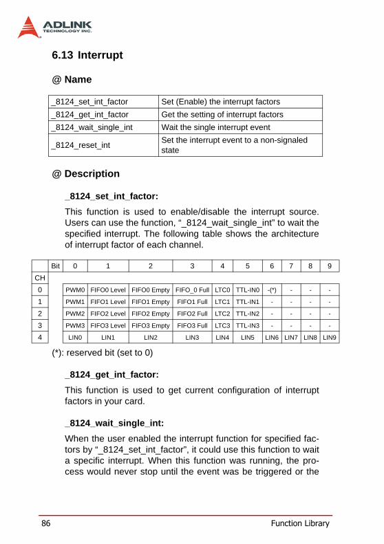
86 Function Library
6.13 Interrupt
@ Name
@ Description
_8124_set_int_factor:
This function is used to enable/disable the interrupt source.Users can use the function, “_8124_wait_single_int” to wait thespecified interrupt. The following table shows the architectureof interrupt factor of each channel.
(*): reserved bit (set to 0)
_8124_get_int_factor:
This function is used to get current configuration of interruptfactors in your card.
_8124_wait_single_int:
When the user enabled the interrupt function for specified fac-tors by “_8124_set_int_factor”, it could use this function to waita specific interrupt. When this function was running, the pro-cess would never stop until the event was be triggered or the
_8124_set_int_factor Set (Enable) the interrupt factors
_8124_get_int_factor Get the setting of interrupt factors
_8124_wait_single_int Wait the single interrupt event
_8124_reset_intSet the interrupt event to a non-signaled state
Bit 0 1 2 3 4 5 6 7 8 9
CH
0 PWM0 FIFO0 Level FIFO0 Empty FIFO_0 Full LTC0 TTL-IN0 -(*) - - -
1 PWM1 FIFO1 Level FIFO1 Empty FIFO1 Full LTC1 TTL-IN1 - - - -
2 PWM2 FIFO2 Level FIFO2 Empty FIFO2 Full LTC2 TTL-IN2 - - - -
3 PWM3 FIFO3 Level FIFO3 Empty FIFO3 Full LTC3 TTL-IN3 - - - -
4 LIN0 LIN1 LIN2 LIN3 LIN4 LIN5 LIN6 LIN7 LIN8 LIN9
Function Library 87
function was time out. This function returns when one of the fol-lowing occurs:
1. The specified interrupt factor is in the signaled state.
2. The time-out interval elapses.
This function checks the current state of the specified interruptfactor. If the state is non-signaled, the calling thread enters thewait state. It uses no processor time while waiting for the INTstate to become signaled or the time-out interval to elapse.
8124_reset_int:
This function sets the specified interrupt event to a non-sig-naled state. This function is usually put into program before the"_8124_wait_single_int" function.
@ Syntax
C/C++ (Windows 2000/XP)I16 _8124_set_int_factor( I16 CardId, I16
Channel, I16 IntFactorsInBit );I16 _8124_get_int_factor( I16 CardId, I16
Channel, I16 *IntFactorsInBit );I16 _8124_wait_single_int( I16 CardId, I16
Channel, I16 FactorBitNum, I32 TimeOutMs );I16 _8124_reset_int( I16 CardId, I16 Channel, I16
FactorBitNum );
Visual Basic (Windows 2000/XP)B_8124_set_int_factor (ByVal CardId As Integer,
ByVal Channel As Integer, ByVal IntFactorsInBit As Integer) As Integer
B_8124_get_int_factor (ByVal CardId As Integer, ByVal Channel As Integer, IntFactorsInBit As Integer) As Integer
B_8124_wait_single_int (ByVal CardId As Integer, ByVal Channel As Integer, ByVal FactorBitNum As Integer, ByVal TimeOutMs As Long) As Integer
B_8124_reset_int( ByVal CardId As Integer, ByVal Channel As Integer, ByVal FactorBitNum As Integer) As Integer
88 Function Library
@ Argument
I16 IntFactorsInBit: Interrupt event factor setting in bit for-mat.
I16 FactorBitNum: Specified the bit number of the IntFactors-InBit.
I32 TimeOutMs: Specify the time-out interval, in milliseconds.
If TimeOutMs is zero, the function tests the states of the specifiedevent and returns immediately. If TimeOutMs is -1, the function’stime-out interval never elapses (infinite)
Function Library 89
6.14 Filtering & Monitoring
@ Name
@ Description
_8124_set_input_filter_enable:
This function is used to enable the digital filter. If the filter isenabled, pulse width of input signals "EA, EB, EZ and LTC" mustlarger than 100 ns or the input signal will be ignore (treat as anoise).
This function is available after Firmware version: 0x13.
_8124_get_noise_detect:
This function is used to detected whether the signal is a noise ornot. If the width of input signal is less than 100 ns, the status willbe turned ON. The status will be cleared after read.
This function is available after Firmware version: 0x13.
_8124_get_pwm_trigger_count:
This function is used to get PWM trigged counter.
This function is only for debug used. Because It does not haveregister latch protection (high word (16-31 bits) latch) of counterwhen register read. Therefore, it could be a problem when counteris count up at mean time you read the counter.
This function is available after Firmware version: 0x13.
_8124_reset_pwm_trigger_count:
This function is used to reset PWM triggered counter.
This function is available after Firmware version: 0x13.
_8124_set_input_filter_enable Enable digital input signal filter
_8124_get_noise_detect Get noise detection status
_8124_get_pwm_trigger_count Get PWM triggered counter
_8124_reset_pwm_trigger_count Reset PWM triggered counter
_8124_get_linear_next_compare Get next linear compare data
_8124_get_linear_remain_trigger_count Get remaining linear trigger count
90 Function Library
_8124_get_linear_next_compare:
This function is used to get the next linear compare data.
This function is only for debug used. It does not have register latchprotection (high word (16-31 bits) latch) of counter when registerread. Therefore, it could be a problem when counter is count up atmean time you read the counter.
This function is available after Firmware version: 0x13.
_8124_get_linear_remain_trigger_count:
This function is used to get remaining triggered counter.
This counter is a count down counter. You can use this function tocheck how many remaining triggered will be output.
This function is available after Firmware version: 0x13.
@ Syntax
C/C++ (Windows 2000/XP)I16 _8124_set_input_filter_enable( I16 CardId,
I16 Channel, I16 Enable );I16 _8124_get_noise_detect( I16 CardId, I16
Channel, I16 *DetectStatus );I16 _8124_get_pwm_trigger_count( I16 CardId, I16
Channel, F64 *PwmCount );I16 _8124_reset_pwm_trigger_count( I16 CardId,
I16 Channel );I16 _8124_get_linear_next_compare( I16 CardId,
I16 SetNum, I32 *CmpData );I16 _8124_get_linear_remain_trigger_count( I16
CardId, I16 SetNum, F64 *Count );
Visual Basic (Windows 2000/XP)
@ Argument
I16 CardId:
I16 Channel: Channel number: 0 ~ 4
Function Library 91
I16 Enable:
0: Disable (Default)
1: Enable
I16 *DetectStatus: Status in bit format.
bit 0: Noise occurred form EA, the signal is less than 100ns, this bit will turn ON
bit 1: Noise occurred form EB, the signal is less than 100ns, this bit will turn ON
bit 2: Noise occurred form EZ, the signal is less than 100ns, this bit will turn ON
bit 3: Noise occurred form LTC, the signal is less than 100ns, this bit will turn ON
bit 4: Pulse lost occurred, If the the signal is fast than decode speed. this bit will turned on.
F64 *PwmCount: 32 bit counter.
I32 *CmpData: Next linear compare data.
F64 *Count: 32 bit count remaining trigger counter.
92 Function Library
6.15 Return Errors
The following table provides a list of possible return value in ourlibrary. If the return value is not zero, it means there are someerrors occurred. This could help you to check the program easierand make it correctly.
Error Codes:
Code Define Description
0 ERR_NoError No Error, function success
-1 ERR_OSVersion Operation System type mismatched
-2 ERR_OpenDriverFailed Open device driver failed - Create driver interface failed
-3 ERR_InsufficientMemory System memory insufficiently
-4 ERR_DeviceNotInitial Cards not be initialized
-5 ERR_NoDeviceFound Cards not found(No card in your system)
-6 ERR_CardIdDuplicate Cards' ID Number duplicate
-7 ERR_DeviceAlreadyInitialed Cards have been initialed
-8 ERR_InterruptNotEnable Cards' interrupt events not enable
-9 ERR_TimeOut Function time-out
-10 ERR_ParametersInvalid Function input parameters are invalid
-11 ERR_SetEEPROM Set data to EEPROM failed
-12 ERR_GetEEPROM Get data from EEPROM failed
-1000 ERR_Win32Error WIN32 API function error, please contact with ADLINK's FAE staff.