Embed Size (px)
Citation preview

Advance Data Sheet: Metamere iAC Series – Non-isolated SMT Power Module
©2009 TDK Innoveta Inc. iACFullDatasheet 072009 7/20/2009
(877) 498-0099 1/16
The iAC Series offers an 80W power module in the industry’s standard surface-mount footprint. The iAC 12Vin series offers an ultra wide input The iAC Series offers an 80W power module in the industry’s standard surface-mount footprint. The iAC 12Vin series offers an ultra wide input voltage range of 6.0-14.0V. It is highly suitable for use in conjunction with 4:1 and 5:1 unregulated bus converters as well as with fully regulated 12Vout bus converters. The open-frame, compact design provides flexibility by performing local voltage conversion of a 12V bus. The low weight, surface mount design is well suited for almost any manufacturing environment.
Metamere iAC Series DC/DC Power Modules 6.0-14V Input, 16A Output
Surface Mount Power Module
Features
• Size - 33mm x 13.5 mm x 8.0 mm (1.3 in. x 0.53 in. x 0.315 in.)
• Surface mountable
• Maximum weight 12g (0.42 oz)
• Up to 80W of output power in high ambient temperature, low airflow environments with minimal power derating
• Calculated MTBF > 13.7M Hours
• Positive logic on/off
• Flexible Output Voltage Sequencing
• Starts with pre-biased output
• Output voltage adjustment – industry standard
• Constant switching frequency
• Remote Sense
• Full, auto-recovery protection: o Input under voltage o Short circuit
• ISO Certified manufacturing facilities
Optional Features
• Negative logic on/off
• No output voltage sequencing
• Industry Standard Narrow 9.6V-14V input voltage range

This page intentionally left blank

Advance Data Sheet: Metamere iAC Series – Non-isolated SMT Power Module
©2009 TDK Innoveta Inc. iACFullDatasheet 072009 7/20/2009
(877) 498-0099 3/16
Mechanical Specification: Dimensions are in mm [in]. Unless otherwise specified tolerances are: x.x ± 0.5 [0.02], x.xx ± 0.25 [0.010]
PIN FUNCTION PIN FUNCTION
1 On/Off 5 Vout
2 Vin 6 Trim
3 Seq 7 Sense
4 Gnd
PIN FUNCTION PIN FUNCTION
1 On/Off 4 Vout
2 Vin 5 Trim
3 Gnd 6 Sense
-000, -001, -004, -005 –Top view Footprint
-002,-003, -006, -007 –Top view Footprint

Advance Data Sheet: Metamere iAC Series – Non-isolated SMT Power Module
©2009 TDK Innoveta Inc. iACFullDatasheet 072009 7/20/2009
(877) 498-0099 4/16
Absolute Maximum Ratings:
Stress in excess of Absolute Maximum Ratings may cause permanent damage to the device.
* Engineering estimate
Input Characteristics:
Unless otherwise specified, specifications apply over all rated Input Voltage, Resistive Load, and Temperature conditions.
Characteristic Min Typ Max Unit Notes & Conditions
Operating Input Voltage (3.63Vand lower outputs) 6.0 9.6
--- 14.0 14.0
Vdc Vdc
-000 through -003 -004 through -007
Operating Input Voltage (greater than 3.63V outputs) 8.3 9.6
--- 14.0 14.0
Vdc Vdc
-000 through -003 -004 through -007
Maximum Input Current --- --- 18* A Vin = 6.0 to Vin,max
Startup Delay Time from application of input voltage --- 4 --- mS Vo = 0 to 0.1*Vo,nom; on/off =on, Io=Io,max, Tc=25˚C
Startup Delay Time from on/off --- 3 --- mS Vo = 0 to 0.1*Vo,nom; Vin = Vi,nom, Io=Io,max,Tc=25˚C
Output Voltage Rise Time --- 5 --- mS Io=Io,max,Tc=25˚C, Vo=0.1 to 0.9*Vo,nom
Input Reflected Ripple --- 30 --- mApp See input/output ripple measurement figure; BW = 20 MHz
Input Ripple Rejection --- 60 --- dB @ 120 Hz
Turn on input voltage --- 4.9 7.3
--- V V
-000 to -003 -004 to -007
Turn off input voltage --- 4.3 5.5
--- V V
-000 to -003 -004 to -007
*Engineering Estimate Caution: The power modules are not internally fused. An external input line normal blow fuse with a maximum value of 30A is required, see the Safety Considerations section of the data sheet.
Characteristic Min Max Unit Notes & Conditions
Continuous Input Voltage -0.25 15 Vdc
Storage Temperature -55 125 ˚C
Operating Temperature Range (Tc) -40 125* ˚C Measured at the location specified in the thermal measurement figure; maximum temperature varies with output current – see curve in the thermal performance section of the data sheet.

Advance Data Sheet: Metamere iAC Series – Non-isolated SMT Power Module
©2009 TDK Innoveta Inc. iACFullDatasheet 072009 7/20/2009
(877) 498-0099 5/16
Electrical Data: Characteristic Min Typ Max Unit Notes & Conditions
Output Voltage Initial Setpoint
-2 - +2 %
Vin=Vin,nom; Io=Io,max; Tc = 25˚C
Output Voltage Tolerance
-2.5 - +3.5 %
Over all rated input voltage, load, and temperature conditions to end of life
Efficiency Vo = 1.2V Vo = 1.5V Vo = 1.8V Vo = 2.5V Vo = 3.3V Vo = 5.0V
--- --- --- --- --- ---
84 86 88 90 92 94
--- --- --- --- --- ---
% % % % % %
Vin= 12.0V; Io=Io,max; Tc = 25˚C
Line Regulation --- 3 10* mV Vin=Vin,min to Vin,max
Load Regulation --- 8 15* mV Io=Io,min to Io,max
Temperature Regulation --- 8 30* mV Tc=Tc,min to Tc,max
Output Current
0 --- 16 A
Output Current Limiting Threshold
--- 28 --- A Vo = 0.9*Vo,nom, Tc<Tc,max)
Short Circuit Current
--- 0.3 --- A Vo = 0.25V, Tc = 25˚C
--- 40
100* mVpp
Output Ripple and Noise Voltage
--- 6 --- mVrms
Measured across one 0.1 uF ceramic capacitor and one 47uF ceramic capacitor – see input/output ripple measurement figure; BW = 20MHz.
Output Voltage Adjustment Range 0.8 --- 5 V
Output Voltage Sense Range --- --- 10 %Vo,nom
Dynamic Response: Recovery Time Transient Voltage
---
---
30
200
---
---
uS mV
di/dt =2.5A/uS, Vin=Vin,nom; load step from 50% to 100% of Io,max
Switching Frequency --- 315 --- kHz Fixed
External Load Capacitance 0 --- 5000*& uF
Vref 0.7 V Required for trim calculation
F 15000 Ω Required for trim calculation
G 1000 Ω Required for trim calculation
*Engineering Estimate & Contact TDK Innoveta for applications that require additional capacitance or very low esr

Advance Data Sheet: Metamere iAC Series – Non-isolated SMT Power Module
©2009 TDK Innoveta Inc. iACFullDatasheet 072009 7/20/2009
(877) 498-0099 6/16
Electrical Characteristics: Typical Efficiency vs. Input Voltage
70
75
80
85
90
95
100
0 2 4 6 8 10 12 14 16
Output Current (A)
Effic
iency, h(%
)
Vin = 6V Vin = 9.6V Vin = 12V Vin = 14V
70
75
80
85
90
95
100
0 2 4 6 8 10 12 14 16
Output Current (A)
Effic
iency, h(%
)
Vin = 6V Vin = 9.6V Vin = 12V Vin = 14V
Vo=1.2V Vo=2.5V
70
75
80
85
90
95
100
0 2 4 6 8 10 12 14 16
Output Current (A)
Effic
iency, h(%
)
Vin = 6V Vin = 9.6V Vin = 12V Vin = 14V
70
75
80
85
90
95
100
0 2 4 6 8 10 12 14 16
Output Current (A)
Effic
iency, h(%
)
Vin = 6V Vin = 9.6V Vin = 12V Vin = 14V
Vo=1.5V Vo=3.3V
70
75
80
85
90
95
100
0 2 4 6 8 10 12 14 16
Output Current (A)
Effic
iency, h(%
)
Vin = 6V Vin = 9.6V Vin = 12V Vin = 14V
70
75
80
85
90
95
100
0 2 4 6 8 10 12 14 16
Output Current (A)
Effic
iency, h(%
)
Vin = 8.3V Vin = 9.6V Vin = 12V Vin = 14V
Vo=1.8V Vo=5V

Advance Data Sheet: Metamere iAC Series – Non-isolated SMT Power Module
©2009 TDK Innoveta Inc. iACFullDatasheet 072009 7/20/2009
(877) 498-0099 7/16
Electrical Characteristics (continued):
Vo=3.3V Typical Output Ripple at nominal Input voltage and full load at Ta=25 degrees
Typical Output Short Circuit Current
Vo=3.3V Typical startup characteristic from on/off at full load. Upper trace - on/off signal, lower trace – output voltage
Vo=3.3V Typical Input Ripple at nominal Input Voltage and full load at Ta=25 degrees. Input capacitors - 2x150uF aluminum and 2x47uF ceramic
Vo=3.3V Typical output voltage transient response to load step from 50% to 100% of full load with output current slew rate of 2.5A/uS
Vo=3.3V Typical output voltage transient response to load step from 50% to 100% of full load with output current slew rate of 2.5A/uS. (Cext = 2x150uF polymer Capacitors

Advance Data Sheet: Metamere iAC Series – Non-isolated SMT Power Module
©2009 TDK Innoveta Inc. iACFullDatasheet 072009 7/20/2009
(877) 498-0099 8/16
Electrical Characteristics (continued):
Typical Output Voltage vs. Input Voltage Characteristics Code: -000, -001, -002, -003 (Input voltage range : 6.0V to 14V)
0
1
2
3
4
3 4 5 6 7 8 9 10
Input Voltage (V)
Outp
ut V
olta
ge (V
)
Io_min = 0A Io_mid = 8A Io_max = 16A
0
2
4
6
8
10
12
14
16
3 4 5 6 7 8 9 10 11 12 13 14
Input Voltage (V)In
put C
urrent (A
)
Io_min = 0A Io_mid = 8A Io_max = 16A
Vo=3.3V Typical Output Voltage vs. Input Voltage Characteristics
Vo=3.3V Typical Input Current vs. Input Voltage Characteristics
0
1
2
3
4
5
6
3 4 5 6 7 8 9 10
Input Voltage (V)
Outp
ut V
olta
ge (V
)
Io_min = 0A Io_mid = 8A Io_max = 16A
0
2
4
6
8
10
12
14
16
3 4 5 6 7 8 9 10 11 12 13 14
Input Voltage (V)
Input C
urrent (A
)
Io_min = 0A Io_mid = 8A Io_max = 16A
Vo=5V Typical Output Voltage vs. Input Voltage Characteristics
Vo=5V Typical Input Current vs. Input Voltage Characteristic

Advance Data Sheet: Metamere iAC Series – Non-isolated SMT Power Module
©2009 TDK Innoveta Inc. iACFullDatasheet 072009 7/20/2009
(877) 498-0099 9/16
Code: -004, -005, -006, -007 (Input voltage range : 9.6V to 14V)
0
1
2
3
4
3 4 5 6 7 8 9 10
Input Voltage (V)
Outp
ut V
olta
ge (V)
Io_min = 0A Io_mid = 8A Io_max = 16A
0
2
4
6
8
10
12
3 4 5 6 7 8 9 10 11 12 13 14
Input Voltage (V)
Input C
urr
ent (A
)
Io_min = 0A Io_mid = 8A Io_max = 16A
Vo=3.3V Typical Output Voltage vs. Input Voltage Characteristics
Vo=3.3V Typical Input Current vs. Input Voltage Characteristics
0
1
2
3
4
5
6
3 4 5 6 7 8 9 10
Input Voltage (V)
Outp
ut V
olta
ge (V)
Io_min = 0A Io_mid = 8A Io_max = 16A
0
2
4
6
8
10
12
14
16
3 4 5 6 7 8 9 10 11 12 13 14
Input Voltage (V)
Input C
urrent (A
)
Io_min = 0A Io_mid = 8A Io_max = 16A
Vo=5V Typical Output Voltage vs. Input Voltage Characteristics
Vo=5V Typical Input Current vs. Input Voltage Characteristics

Advance Data Sheet: Metamere iAC Series – Non-isolated SMT Power Module
©2009 TDK Innoveta Inc. iACFullDatasheet 072009 7/20/2009
(877) 498-0099 10/16
Thermal Performance:
0
2
4
6
8
10
12
14
16
40 50 60 70 80 90 100 110 120
Temperature (oC)
Outp
ut C
urrent (A
)
NC
0.5 m/s (100 LFM)
1.0 m/s (200 LFM)
2.0 m/s (400 LFM)
Tc, Thermal Limit
0
2
4
6
8
10
12
14
16
40 50 60 70 80 90 100 110 120
Temperature (oC)
Outp
ut C
urr
ent (A
)
NC
0.5 m/s (100 LFM)
1.0 m/s (200 LFM)
2.0 m/s (400 LFM)
Tc, Thermal Limit
Vo=1.8V, Vin=12V maximum output current vs. ambient temperature at nominal input voltage for airflow rates natural convection to 400lfm with airflow from pin 2 to pin 3 (Best Direction).
Vo=3.3V, Vin=12V maximum output current vs. ambient temperature at nominal input voltage for airflow rates natural convection to 400lfm with airflow from pin 2 to pin 3 (Best Direction).
0
2
4
6
8
10
12
14
16
40 50 60 70 80 90 100 110 120
Temperature (oC)
Outp
ut C
urr
ent (A
)
NC
0.5 m/s (100 LFM)
1.0 m/s (200 LFM)
2.0 m/s (400 LFM)
Tc, Thermal Limit
Vo=1.8V, Vin=12V maximum output current vs. ambient temperature at nominal input voltage for airflow rates natural convection to 400lfm with airflow from pin 1 to pin 2 (Worst Direction).
iAC12016A008V thermal measurement location and airflow orientation – top view
The thermal curves provided are based upon measurements made in TDK Innoveta’s experimental test setup that is described in the Thermal Management section. Due to the large number of variables in system design, TDK Innoveta recommends that the user verify the module’s thermal performance in the end application. The critical component should be thermo coupled and monitored, and should not exceed the temperature limit specified in the derating curve above. It is critical that the thermocouple be mounted in a manner that gives direct thermal contact or significant measurement errors may result. TDK Innoveta can provide modules with a thermocouple pre-mounted to the critical component for system verification tests.

Advance Data Sheet: Metamere iAC Series – Non-isolated SMT Power Module
©2009 TDK Innoveta Inc. iACFullDatasheet 072009 7/20/2009
(877) 498-0099 11/16
Soldering Information: iAC surface mountable power modules are intended to be compatible with standard surface mount component soldering processes and either hand placed or automatically picked and placed. The figure below shows the position for vacuum pick up. The maximum weight of the power module is 12g (0.42 oz.). Improper handling or cleaning processes can adversely affect the appearance, testability, and reliability of the power modules. The iAC product is a moisture sensitivity level 2 device. Contact TDK Innoveta technical support for guidance regarding proper handling, cleaning, and soldering of TDK Innoveta’s power modules.
Reflow Soldering The iAC platform is an open frame power module manufactured with SMT (surface mount technology). Due to the high thermal mass of the power module and sensitivity to heat of some SMT components, extra caution should be taken when reflow soldering. Failure to follow the reflow soldering guidelines described below may result in permanent damage and/or affect performance of the power modules. The iAC power modules can be soldered using natural convection, forced convection, IR (radiant infrared), and convection/IR reflow technologies. The module should be thermally characterized in its application to develop a temperature profile. Thermal couples should be mounted to pin 2 and pin 6 and be monitored. The temperatures in the figure are maximum limits. Oven temperature and conveyer belt speeds should be controlled to ensure these limits are not exceeded. To ensure a reliable solder joint, a minimum solder paste volume of 1.25 mm3 (76,500 cubic mils) is required with a minimum solder paste thickness of at least 0.13 mm (0.0051 in.). In most manufacturing processes, the required solder paste can be applied with a standard 6 mil stencil. iAC power modules are tested for lead coplanarity as part of the manufacturing process.
Drawing to be provided in future revision
Drawing to be provided in future revision
iAC Power Module maximum pin temperature profile iAC Power Module suggested reflow-soldering profile

Advance Data Sheet: Metamere iAC Series – Non-isolated SMT Power Module
©2009 TDK Innoveta Inc. iACFullDatasheet 072009 7/20/2009
(877) 498-0099 12/16
Thermal Management: An important part of the overall system design process is thermal management; thermal design must be considered at all levels to ensure good reliability and lifetime of the final system. Superior thermal design and the ability to operate in severe application environments are key elements of a robust, reliable power module. A finite amount of heat must be dissipated from the power module to the surrounding environment. This heat is transferred by the three modes of heat transfer: convection, conduction and radiation. While all three modes of heat transfer are present in every application, convection is the dominant mode of heat transfer in most applications. However, to ensure adequate cooling and proper operation, all three modes should be considered in a final system configuration. The open frame design of the power module provides an air path to individual components. This air path improves convection cooling to the surrounding environment, which reduces areas of heat concentration and resulting hot spots.
Test Setup: The thermal performance data of the power module is based upon measurements obtained from a wind tunnel test with the setup shown in the wind tunnel figure. This thermal test setup replicates the typical thermal environments encountered in most modern electronic systems with distributed power architectures. The electronic equipment in networking, telecom, wireless, and advanced computer systems operates in similar environments and utilizes vertically mounted PCBs or circuit cards in cabinet racks. The power module, as shown in the figure, is mounted on a printed circuit board (PCB) and is vertically oriented within the wind tunnel. The cross section of the airflow passage is rectangular. The spacing between the top of the module and a parallel facing PCB is kept at a constant (0.5 in). The power module’s orientation with respect to the airflow direction can have a significant impact on the module’s thermal performance.
Thermal Derating: For proper application of the power module in a given thermal environment, output current derating curves are provided as a design guideline on the Thermal Performance section for the
power module of interest. The module temperature should be measured in the final system configuration to ensure proper thermal management of the power module. For thermal performance verification, the module temperature should be measured at the component indicated in the thermal measurement location figure on the thermal performance page for the power module of interest. In all conditions, the power module should be operated below the maximum operating temperature shown on the derating curve. For improved design margins and enhanced system reliability, the power module may be operated at temperatures below the maximum rated
operating temperature.
Heat transfer by convection can be enhanced by increasing the airflow rate that the power module experiences. The maximum output current of the power module is a function of ambient temperature (TAMB) and airflow rate as shown in the thermal performance figures on the thermal performance page for the power module of interest. The curves in the figures are shown for natural convection through 2 m/s (400 ft/min). The data for the natural convection condition has been collected at 0.3 m/s (60 ft/min) of airflow, which is the typical airflow generated by other heat dissipating components in many of the systems that these types of modules are used in. In the final system configurations, the airflow rate for the natural convection condition can vary due to temperature gradients from other heat dissipating components.
AIRFLOW
Air Velocity and Ambient Temperature Measurement Location
A I R F L OW
12.7 (0.50)
Module Centerline
Air Passage Centerline
Adjacent PCB
76 (3.0)
Wind Tunnel Test Setup Figure Dimensions are in millimeters and (inches).

Advance Data Sheet: Metamere iAC Series – Non-isolated SMT Power Module
©2009 TDK Innoveta Inc. iACFullDatasheet 072009 7/20/2009
(877) 498-0099 13/16
Operating Information:
Over-Current Protection: The power modules have short circuit protection to protect the module during severe overload conditions. During overload conditions, the power modules may protect themselves by entering a hiccup current limit mode. The modules will operate normally once the output current returns to the specified operating range. Remote On/Off: - The power modules have an internal remote on/off circuit. The user must supply an open-collector or compatible switch between the GND pin and the on/off pin. The maximum voltage generated by the power module at the on/off terminal is 15V. The maximum allowable leakage current of the switch is 10uA. The switch must be capable of maintaining a low signal Von/off < 0.3V while sinking 1mA. The standard on/off logic is positive logic. The power module will turn on if terminal 1 (on/off) is left open and will be off if terminal 1 is connected to terminal GND. If the positive logic circuit is not being used, terminal 1 should be left open.
GND
On/ Off
Vin (+)
On/Off Circuit for positive logic An optional negative logic is available. In the circuit configuration shown the power module will turn on if the external switch is on and it will be off if the on/off pin is pulled up to Vin by an external 40Kohm resistor. If the negative logic feature is not being used, terminal 1 should be left open.
GND
On/ Off
Vin (+)Rpullup
On/Off Circuit for negative logic Remote Sense: The power modules feature remote sense to compensate for the effect of output distribution drops. The output voltage sense range defines the maximum voltage allowed between the output power terminals and output sense terminals, and it is found on the electrical data page for the power module of interest. If the remote sense feature is not being used, the Sense terminal should be connected to the Vo terminal.
The output voltage at the Vo terminal can be increased by either the remote sense or the output voltage adjustment feature. The maximum voltage increase allowed is the larger of the remote sense range or the output voltage adjustment range; it is not the sum of both.
As the output voltage increases due to the use of the remote sense, the maximum output current may need to be decreased for the power module to remain below its maximum power rating.
Output Voltage Adjustment: The output voltage of the power module may be adjusted by using an external resistor connected between the Vout trim terminal and GND terminal. If the output voltage adjustment feature is not used, trim terminal should be left open. Care should be taken to avoid injecting noise into the power module’s trim pin. A small 0.01uF capacitor between the power module’s trim pin and GND pin may help avoid this.
Advance Data Sheet: Metamere iAC Series – Non-isolated SMT Power Module
©2009 TDK Innoveta Inc. iACFullDatasheet 072009 7/20/2009
(877) 498-0099 14/16
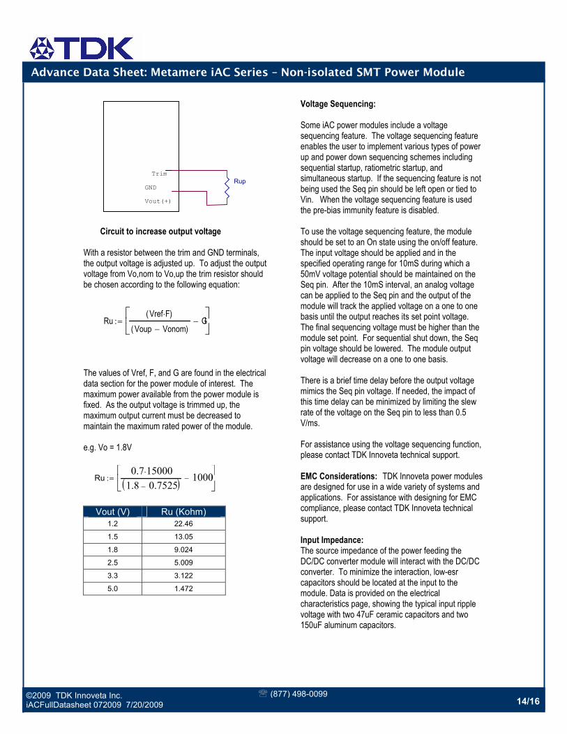
Trim
Vout(+)
Rup GND
Circuit to increase output voltage
With a resistor between the trim and GND terminals, the output voltage is adjusted up. To adjust the output voltage from Vo,nom to Vo,up the trim resistor should be chosen according to the following equation:
RuVref F⋅( )
Voup Vonom−( )G−
:=
The values of Vref, F, and G are found in the electrical data section for the power module of interest. The maximum power available from the power module is fixed. As the output voltage is trimmed up, the maximum output current must be decreased to maintain the maximum rated power of the module. e.g. Vo = 1.8V
Ru0.7 15000⋅
1.8 0.7525−( ) 1000−
:=
Vout (V) Ru (Kohm)
1.2 22.46
1.5 13.05
1.8 9.024
2.5 5.009
3.3 3.122
5.0 1.472
Voltage Sequencing: Some iAC power modules include a voltage sequencing feature. The voltage sequencing feature enables the user to implement various types of power up and power down sequencing schemes including sequential startup, ratiometric startup, and simultaneous startup. If the sequencing feature is not being used the Seq pin should be left open or tied to Vin. When the voltage sequencing feature is used the pre-bias immunity feature is disabled. To use the voltage sequencing feature, the module should be set to an On state using the on/off feature. The input voltage should be applied and in the specified operating range for 10mS during which a 50mV voltage potential should be maintained on the Seq pin. After the 10mS interval, an analog voltage can be applied to the Seq pin and the output of the module will track the applied voltage on a one to one basis until the output reaches its set point voltage. The final sequencing voltage must be higher than the module set point. For sequential shut down, the Seq pin voltage should be lowered. The module output voltage will decrease on a one to one basis. There is a brief time delay before the output voltage mimics the Seq pin voltage. If needed, the impact of this time delay can be minimized by limiting the slew rate of the voltage on the Seq pin to less than 0.5 V/ms. For assistance using the voltage sequencing function, please contact TDK Innoveta technical support. EMC Considerations: TDK Innoveta power modules are designed for use in a wide variety of systems and applications. For assistance with designing for EMC compliance, please contact TDK Innoveta technical support. Input Impedance: The source impedance of the power feeding the DC/DC converter module will interact with the DC/DC converter. To minimize the interaction, low-esr capacitors should be located at the input to the module. Data is provided on the electrical characteristics page, showing the typical input ripple voltage with two 47uF ceramic capacitors and two 150uF aluminum capacitors.

Advance Data Sheet: Metamere iAC Series – Non-isolated SMT Power Module
©2009 TDK Innoveta Inc. iACFullDatasheet 072009 7/20/2009
(877) 498-0099 15/16
Reliability:
The power modules are designed using TDK Innoveta’s stringent design guidelines for component derating, product qualification, and design reviews. The MTBF is calculated to be greater than 13.7M hours at full output power and Ta = 40˚C using the Telcordia SR-332 calculation method.
Quality:
TDK Innoveta’s product development process incorporates advanced quality planning tools such as FMEA and Cpk analysis to ensure designs are robust and reliable. All products are assembled at ISO certified assembly plants.
Input/Output Ripple and Noise Measurements:
100KHz
Voutput Cext
1
2
+
1uH 1 2
esr<0.1
Battery
100KHz
+ RLoad
1
2 esr<0.1 -
Vinput 200uF
1
2
Ground Plane
300uF 1
2 -
The input reflected ripple is measured with a current probe and oscilloscope. The ripple current is the current through the 1uH inductor.
The output ripple measurement is made approximately 9 cm (3.5 in.) from the power module using an oscilloscope and BNC socket. The capacitor Cext is located about 5 cm (2 in.) from the power module; its value varies from code to code and is found on the electrical data page for the power module of interest under the ripple & noise voltage specification in the Notes & Conditions column.
Safety Considerations: As of the publishing date, certain safety agency approvals may have been received on the iAC series and others may still be pending. Check with TDK Innoveta for the latest status of safety approvals on the iAC product line. For safety agency approval of the system in which the DC-DC power module is installed, the power module must be installed in compliance with the creepage and clearance requirements of the safety agency.
To preserve maximum flexibility, the power modules are not internally fused. An external input line normal blow fuse with a maximum value of 30A is required by safety agencies. A lower value fuse can be selected based upon the maximum dc input current and maximum inrush energy of the power module. Warranty: TDK Innoveta’s comprehensive line of power solutions includes efficient, high-density DC-DC converters. TDK Innoveta offers a three-year limited warranty. Complete warranty information is listed on our web site or is available upon request from TDK Innoveta.

Advance Data Sheet: Metamere iAC Series – Non-isolated SMT Power Module
©2009 TDK Innoveta Inc. iACFullDatasheet 072009 7/20/2009
(877) 498-0099 16/16
Information furnished by TDK Innoveta is believed to be accurate and reliable. However, TDK Innoveta assumes no responsibility
for its use, nor for any infringement of patents or other rights of third parties, which may result from its use. No license is granted
by implication or otherwise under any patent or patent rights of TDK Innoveta. TDK Innoveta components are not designed to be
used in applications, such as life support systems, wherein failure or malfunction could result in injury or death. All sales are
subject to TDK Innoveta’s Terms and Conditions of Sale, which are available upon request. Specifications are subject to change
without notice.
Specifications are subject to change without notice.
is a trademark or registered trademark of TDK Corporation.
3320 Matrix Drive, Suite 100 Richardson, TX 75802
Phone (877) 498-0099 Toll Free (469) 916-4747 Fax (877) 498-0143 Toll Free (214) 239-3101 [email protected] http://www.tdkinnoveta.com/