Embed Size (px)
Citation preview
ADSP-TS101S MP System Simulation and Analysis Rev. 1.2 March 12, 2002
Copyright © 2002, Plexus Corp. Signal Integrity Analysis Group
Plexus Corp – Signal Integrity Analysis Group 400 Amherst St., Suite 301, Nashua, New Hampshire, 03063
Phone: (603) 864-1300 Internet: www.plexus.com
Copyright © 2002 Plexus Corp 2 of 24
TABLE OF CONTENTS 1 OVERVIEW .....................................................................................................................................3 2 THEORETICAL FOUNDATION ......................................................................................................4
2.1 SIMULATION RESULTS.......................................................................................................5-8 3 TIMING ANALYSIS BACKGROUND ........................................................................................9-11
3.1 TIMING ANALYSIS DATA......................................................................................................12
4 TERMINATION STRATEGY .........................................................................................................17 5 PHYSICAL IMPLEMENTATION ...................................................................................................18
5.1 SYSTEM CLOCK DISTRIBUTION.........................................................................................19
6 PCB STACK-UP AND DESIGN REQUIREMENTS......................................................................20 6.1 PLACEMENT AND ROUTING ...............................................................................................22
7 CONCLUSION...............................................................................................................................24
Plexus Corp – Signal Integrity Analysis Group 400 Amherst St., Suite 301, Nashua, New Hampshire, 03063
Phone: (603) 864-1300 Internet: www.plexus.com
Copyright © 2002 Plexus Corp 3 of 24
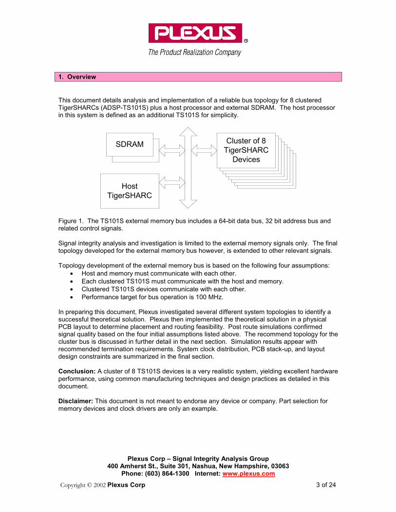
1. Overview This document details analysis and implementation of a reliable bus topology for 8 clustered TigerSHARCs (ADSP-TS101S) plus a host processor and external SDRAM. The host processor in this system is defined as an additional TS101S for simplicity.
SDRAM
HostTigerSHARC
Cluster of 8TigerSHARC
Devices
Figure 1. The TS101S external memory bus includes a 64-bit data bus, 32 bit address bus and related control signals. Signal integrity analysis and investigation is limited to the external memory signals only. The final topology developed for the external memory bus however, is extended to other relevant signals. Topology development of the external memory bus is based on the following four assumptions:
• Host and memory must communicate with each other. • Each clustered TS101S must communicate with the host and memory. • Clustered TS101S devices communicate with each other. • Performance target for bus operation is 100 MHz.
In preparing this document, Plexus investigated several different system topologies to identify a successful theoretical solution. Plexus then implemented the theoretical solution in a physical PCB layout to determine placement and routing feasibility. Post route simulations confirmed signal quality based on the four initial assumptions listed above. The recommend topology for the cluster bus is discussed in further detail in the next section. Simulation results appear with recommended termination requirements. System clock distribution, PCB stack-up, and layout design constraints are summarized in the final section. Conclusion: A cluster of 8 TS101S devices is a very realistic system, yielding excellent hardware performance, using common manufacturing techniques and design practices as detailed in this document. Disclaimer: This document is not meant to endorse any device or company. Part selection for memory devices and clock drivers are only an example.
Plexus Corp – Signal Integrity Analysis Group 400 Amherst St., Suite 301, Nashua, New Hampshire, 03063
Phone: (603) 864-1300 Internet: www.plexus.com
Copyright © 2002 Plexus Corp 4 of 24
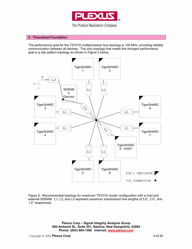
2. Theoretical Foundation The performance goal for the TS101S multiprocessor bus topology is 100 MHz, providing reliable communication between all devices. The only topology that meets this stringent performance goal is a star pattern topology as shown in Figure 2 below.
L1
L2
TigerSHARC1
TigerSHARC2
TigerSHARC3
TigerSHARC4
TigerSHARC5
TigerSHARC6
TigerSHARC7
TigerSHARC8
SDRAM2
Devices
TigerSHARC9 - HOST
L1
L1
L1
L1
L1
L1L1
L1
L3C
R
PIN 1 INDICATOR
VIA CONNECTION Figure 2. Recommended topology for maximum TS101S cluster configuration with a host and external SDRAM. L1, L2, and L3 represent maximum transmission line lengths of 3.0”, 2.0”, and 1.0” respectively.
Plexus Corp – Signal Integrity Analysis Group 400 Amherst St., Suite 301, Nashua, New Hampshire, 03063
Phone: (603) 864-1300 Internet: www.plexus.com
Copyright © 2002 Plexus Corp 5 of 24
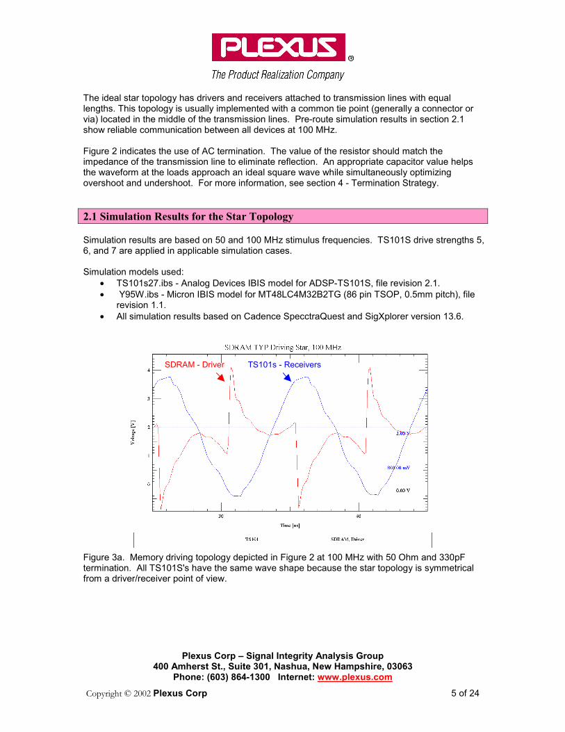
The ideal star topology has drivers and receivers attached to transmission lines with equal lengths. This topology is usually implemented with a common tie point (generally a connector or via) located in the middle of the transmission lines. Pre-route simulation results in section 2.1 show reliable communication between all devices at 100 MHz. Figure 2 indicates the use of AC termination. The value of the resistor should match the impedance of the transmission line to eliminate reflection. An appropriate capacitor value helps the waveform at the loads approach an ideal square wave while simultaneously optimizing overshoot and undershoot. For more information, see section 4 - Termination Strategy. 2.1 Simulation Results for the Star Topology Simulation results are based on 50 and 100 MHz stimulus frequencies. TS101S drive strengths 5, 6, and 7 are applied in applicable simulation cases. Simulation models used:
• TS101s27.ibs - Analog Devices IBIS model for ADSP-TS101S, file revision 2.1. • Y95W.ibs - Micron IBIS model for MT48LC4M32B2TG (86 pin TSOP, 0.5mm pitch), file
revision 1.1. • All simulation results based on Cadence SpecctraQuest and SigXplorer version 13.6.
Figure 3a. Memory driving topology depicted in Figure 2 at 100 MHz with 50 Ohm and 330pF termination. All TS101S's have the same wave shape because the star topology is symmetrical from a driver/receiver point of view.
SDRAM - Driver TS101s - Receivers
Plexus Corp – Signal Integrity Analysis Group 400 Amherst St., Suite 301, Nashua, New Hampshire, 03063
Phone: (603) 864-1300 Internet: www.plexus.com
Copyright © 2002 Plexus Corp 6 of 24
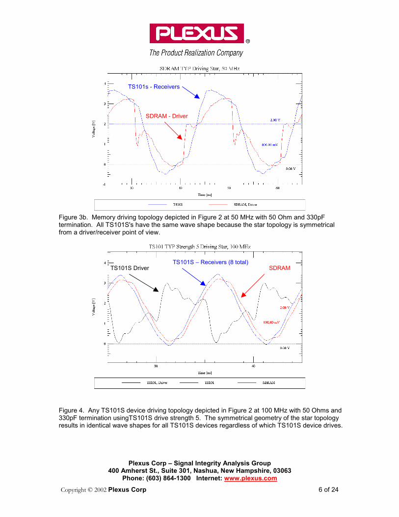
Figure 3b. Memory driving topology depicted in Figure 2 at 50 MHz with 50 Ohm and 330pF termination. All TS101S's have the same wave shape because the star topology is symmetrical from a driver/receiver point of view.
Figure 4. Any TS101S device driving topology depicted in Figure 2 at 100 MHz with 50 Ohms and 330pF termination usingTS101S drive strength 5. The symmetrical geometry of the star topology results in identical wave shapes for all TS101S devices regardless of which TS101S device drives.
TS101S Driver TS101S – Receivers (8 total)
SDRAM
SDRAM - Driver
TS101s - Receivers
Plexus Corp – Signal Integrity Analysis Group 400 Amherst St., Suite 301, Nashua, New Hampshire, 03063
Phone: (603) 864-1300 Internet: www.plexus.com
Copyright © 2002 Plexus Corp 7 of 24
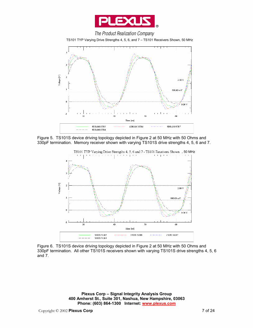
Figure 5. TS101S device driving topology depicted in Figure 2 at 50 MHz with 50 Ohms and 330pF termination. Memory receiver shown with varying TS101S drive strengths 4, 5, 6 and 7.
Figure 6. TS101S device driving topology depicted in Figure 2 at 50 MHz with 50 Ohms and 330pF termination. All other TS101S receivers shown with varying TS101S drive strengths 4, 5, 6 and 7.
TS101 TYP Varying Drive Strengths 4, 5, 6, and 7 – TS101 Receivers Shown, 50 MHz
, 50 MHz
Plexus Corp – Signal Integrity Analysis Group 400 Amherst St., Suite 301, Nashua, New Hampshire, 03063
Phone: (603) 864-1300 Internet: www.plexus.com
Copyright © 2002 Plexus Corp 8 of 24
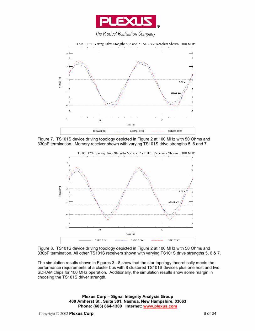
Figure 7. TS101S device driving topology depicted in Figure 2 at 100 MHz with 50 Ohms and 330pF termination. Memory receiver shown with varying TS101S drive strengths 5, 6 and 7.
Figure 8. TS101S device driving topology depicted in Figure 2 at 100 MHz with 50 Ohms and 330pF termination. All other TS101S receivers shown with varying TS101S drive strengths 5, 6 & 7. The simulation results shown in Figures 3 - 8 show that the star topology theoretically meets the performance requirements of a cluster bus with 8 clustered TS101S devices plus one host and two SDRAM chips for 100 MHz operation. Additionally, the simulation results show some margin in choosing the TS101S driver strength.
, 100 MHz
, 100 MHz
Plexus Corp – Signal Integrity Analysis Group 400 Amherst St., Suite 301, Nashua, New Hampshire, 03063
Phone: (603) 864-1300 Internet: www.plexus.com
Copyright © 2002 Plexus Corp 9 of 24
3. Timing Analysis - Background Overview: This section examines the timing of the Cluster of 8 TS101S Devices and TS101S to Memory timing. This document refers to timing in the classical terms. The base line calculations examine subsets of timing data. These subsets are plugged into the classical equations and determine the timing margin. Flight time and its relationship to AC timing specifications is examined prior to investigating the detailed timing calculations. This background information is present in order to clarify how the timing margins were defined. The measurements in this section are for a suggested layout and stack-up. Other systems may be different. Some of the numbers have been rounded up or down to allow easier understanding of their impact on the equations. Conservative estimates are used in places where timing impact is not significant. Flight time background: Plexus engineers have run I/O simulation using IBIS models in order to calculate the flight times of the signals. The IBIS models include data for min, typ, and max process corners. Devices that meet the timing specification don’t all run at exactly the same speed. The corner process information accounts for the slow and fast variations within the operational parameters of the specification. This is important when checking the worst case conditions. For example, consider the worst case setup calculation. It is important to examine the signal performance of the data path with the simulation parameters set for the slow process and with the clock paths set to the fast process. AC Specifications and Flight times: Devices are assembled on printed circuit boards with copper interconnects. The TS101S output rise times are very fast and hence the copper traces act as transmission lines. Therefore, it is important to consider these delays in calculating a system’s worst case timing performance. Plexus examined the output of the TS101S and its interaction with the copper trace when modeling the system in a signal integrity tool. It is important to establish the relationship of the timing specifications (AC specifications) and the actual PCB traces. If ‘rule of thumb’ approximations are applied the timing analysis will be flawed with either overly conservative or underestimated approximations. Measurement of simulated flight times and trace velocities are easy to make in an SI tool. Correlation of flight times to the AC specifications and worst case system timing however, is a bit more difficult.
Copy
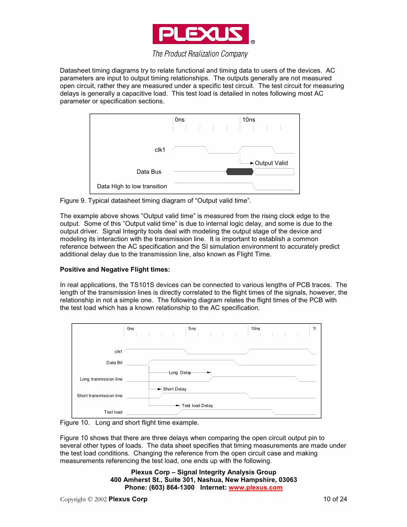
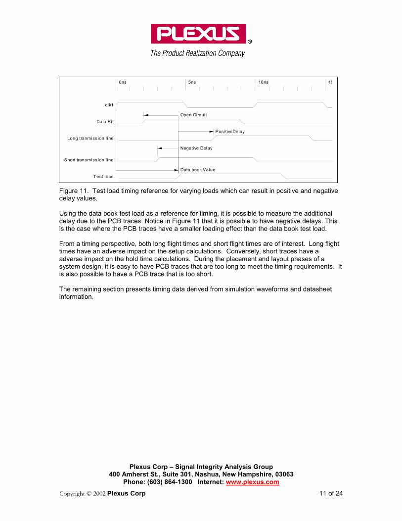
Datasheet timing diagrams try to relate functional and timing data to users of the devices. AC parameters are input to output timing relationships. The outputs generally are not measured open circuit, rather they are measured under a specific test circuit. The test circuit for measuring delays is generally a capacitive load. This test load is detailed in notes following most AC parameter or specification sections. Figure 9. Typical datasheet timing diagram of “Output valid time”. The example above shows ”Output valid time” is measured from the rising clock edge to the output. Some of this ”Output valid time” is due to internal logic delay, and some is due to the output driver. Signal Integrity tools deal with modeling the output stage of the device and modeling its interaction with the transmission line. It is important to establish a common reference between the AC specification and the SI simulation environment to accurately predict additional delay due to the transmission line, also known as Flight Time. Positive and Negative Flight times: In real applications, the TS101S devices can be connected to various lengths of PCB traces. The length of the transmission lines is directly correlated to the flight times of the signals, however, the relationship in not a simple one. The following diagram relates the flight times of the PCB with the test load which has a known relationship to the AC specification. Figu Figusevethe tmea
Output Valid
0ns 10ns
clk1
Data Bus
Data High to low transition
0ns 5ns 10ns 15
Plexus Corp – Signal Integrity Analysis Group 400 Amherst St., Suite 301, Nashua, New Hampshire, 03063
Phone: (603) 864-1300 Internet: www.plexus.com
right © 2002 Plexus Corp 10 of 24
re 10. Long and short flight time example.
re 10 shows that there are three delays when comparing the open circuit output pin to ral other types of loads. The data sheet specifies that timing measurements are made under est load conditions. Changing the reference from the open circuit case and making surements referencing the test load, one ends up with the following.
Test load Delay
Short Delay
Long Delay
clk1
Data Bit
Long tranmission line
Short transmission line
Test load
C
Fd Udi Ftasi Ti
0ns 5ns 10ns 15
Plexus Corp – Signal Integrity Analysis Group 400 Amherst St., Suite 301, Nashua, New Hampshire, 03063
Phone: (603) 864-1300 Internet: www.plexus.com
opyright © 2002 Plexus Corp 11 of 24
igure 11. Test load timing reference for varying loads which can result in positive and negative elay values.
sing the data book test load as a reference for timing, it is possible to measure the additional elay due to the PCB traces. Notice in Figure 11 that it is possible to have negative delays. This
s the case where the PCB traces have a smaller loading effect than the data book test load.
rom a timing perspective, both long flight times and short flight times are of interest. Long flight imes have an adverse impact on the setup calculations. Conversely, short traces have a dverse impact on the hold time calculations. During the placement and layout phases of a ystem design, it is easy to have PCB traces that are too long to meet the timing requirements. It
s also possible to have a PCB trace that is too short.
he remaining section presents timing data derived from simulation waveforms and datasheet nformation.
Data book Value
Negative Delay
PositiveDelay
Open Circuit
c lk1
Data Bit
Long tranmiss ion l ine
Short transmiss ion l ine
T es t load
Plexus Corp – Signal Integrity Analysis Group 400 Amherst St., Suite 301, Nashua, New Hampshire, 03063
Phone: (603) 864-1300 Internet: www.plexus.com
Copyright © 2002 Plexus Corp 12 of 24
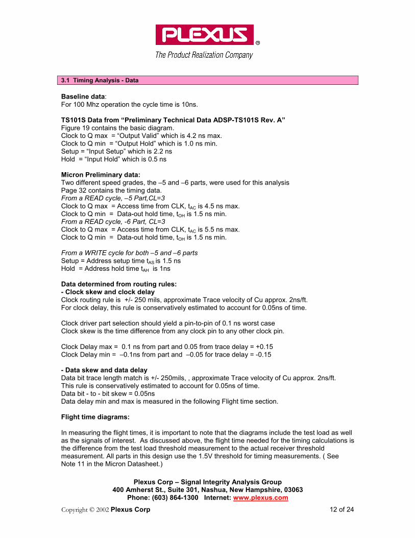
3.1 Timing Analysis - Data Baseline data: For 100 Mhz operation the cycle time is 10ns. TS101S Data from “Preliminary Technical Data ADSP-TS101S Rev. A” Figure 19 contains the basic diagram. Clock to Q max = “Output Valid” which is 4.2 ns max. Clock to Q min = “Output Hold” which is 1.0 ns min. Setup = “Input Setup” which is 2.2 ns Hold = “Input Hold” which is 0.5 ns Micron Preliminary data: Two different speed grades, the –5 and –6 parts, were used for this analysis Page 32 contains the timing data. From a READ cycle, –5 Part,CL=3 Clock to Q max = Access time from CLK, tAC is 4.5 ns max. Clock to Q min = Data-out hold time, tOH is 1.5 ns min. From a READ cycle, -6 Part, CL=3 Clock to Q max = Access time from CLK, tAC is 5.5 ns max. Clock to Q min = Data-out hold time, tOH is 1.5 ns min. From a WRITE cycle for both –5 and –6 parts Setup = Address setup time tAS is 1.5 ns Hold = Address hold time tAH is 1ns Data determined from routing rules: - Clock skew and clock delay Clock routing rule is +/- 250 mils, approximate Trace velocity of Cu approx. 2ns/ft. For clock delay, this rule is conservatively estimated to account for 0.05ns of time.
Clock driver part selection should yield a pin-to-pin of 0.1 ns worst case Clock skew is the time difference from any clock pin to any other clock pin. Clock Delay max = 0.1 ns from part and 0.05 from trace delay = +0.15 Clock Delay min = –0.1ns from part and –0.05 for trace delay = -0.15
- Data skew and data delay Data bit trace length match is +/- 250mils, , approximate Trace velocity of Cu approx. 2ns/ft. This rule is conservatively estimated to account for 0.05ns of time. Data bit - to - bit skew = 0.05ns Data delay min and max is measured in the following Flight time section. Flight time diagrams: In measuring the flight times, it is important to note that the diagrams include the test load as well as the signals of interest. As discussed above, the flight time needed for the timing calculations is the difference from the test load threshold measurement to the actual receiver threshold measurement. All parts in this design use the 1.5V threshold for timing measurements. ( See Note 11 in the Micron Datasheet.)
Plexus Corp – Signal Integrity Analysis400 Amherst St., Suite 301, Nashua, New Ham
Phone: (603) 864-1300 Internet: www.ple
Copyright © 2002 Plexus Corp
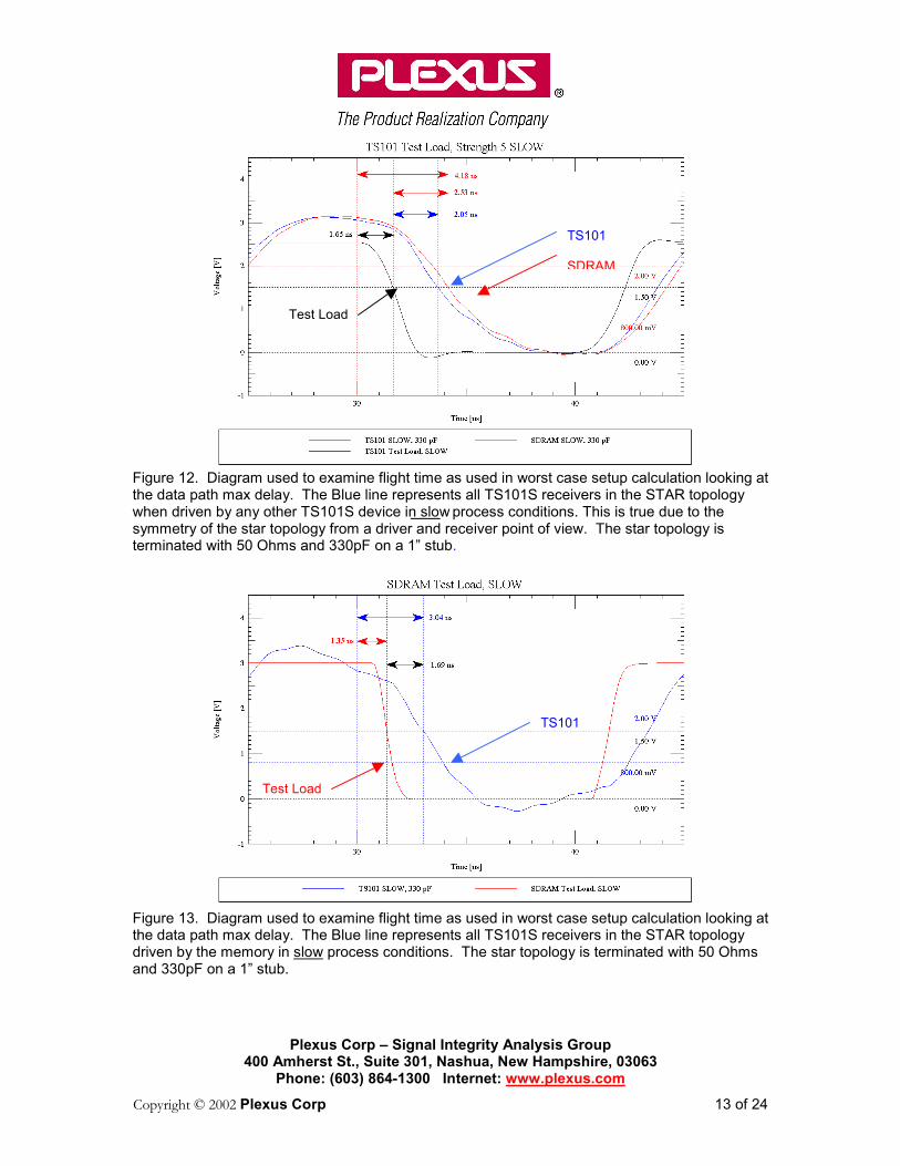
Figure 12. Diagram used to examine flight time as used in worst cthe data path max delay. The Blue line represents all TS101S recwhen driven by any other TS101S device in slow process conditiosymmetry of the star topology from a driver and receiver point of vterminated with 50 Ohms and 330pF on a 1” stub. Figure 13. Diagram used to examine flight time as used in worst cthe data path max delay. The Blue line represents all TS101S recdriven by the memory in slow process conditions. The star topoloand 330pF on a 1” stub.
Test Load
Test Load
TS1
TS101 SDRAM
Group pshire, 03063 xus.com
13 of 24
ase setup calculation looking at eivers in the STAR topology ns. This is true due to the iew. The star topology is
ase setup calculation looking at eivers in the STAR topology gy is terminated with 50 Ohms
01
Plexus Corp – Signal Integrity Analysis Group400 Amherst St., Suite 301, Nashua, New Hampshire,
Phone: (603) 864-1300 Internet: www.plexus.co
Copyright © 2002 Plexus Corp
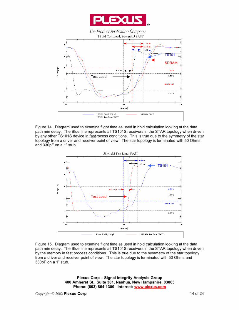
Figure 14. Diagram used to examine flight time as used in hold calculationpath min delay. The Blue line represents all TS101S receivers in the STAby any other TS101S device in fast process conditions. This is true due to ttopology from a driver and receiver point of view. The star topology is termand 330pF on a 1” stub. Figure 15. Diagram used to examine flight time as used in hold calculationpath min delay. The Blue line represents all TS101S receivers in the STAby the memory in fast process conditions. This is true due to the symmetrfrom a driver and receiver point of view. The star topology is terminated w330pF on a 1” stub.
Test Load
Test Load
TS101 SDRAM
looking at the data R topology when driven he symmetry of the star inated with 50 Ohms
TS101
03063 m 14 of 24
looking at the data R topology when driven y of the star topology ith 50 Ohms and
Plexus Corp – Signal Integrity Analysis Group 400 Amherst St., Suite 301, Nashua, New Hampshire, 03063
Phone: (603) 864-1300 Internet: www.plexus.com
Copyright © 2002 Plexus Corp 15 of 24
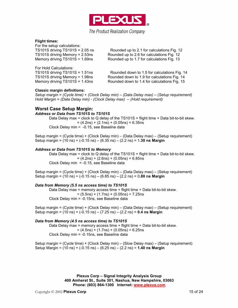
Flight times: For the setup calculations: TS101S driving TS101S = 2.05 ns Rounded up to 2.1 for calculations Fig. 12 TS101S driving Memory = 2.53ns Rounded up to 2.6 for calculations Fig. 12 Memory driving TS101S = 1.69ns Rounded up to 1.7 for calculations Fig. 13 For Hold Calculations: TS101S driving TS101S = 1.51ns Rounded down to 1.5 for calculations Fig. 14 TS101S driving Memory = 1.98ns Rounded down to 1.9 for calculations Fig. 14 Memory driving TS101S = 1.43ns Rounded down to 1.4 for calculations Fig. 15 Classic margin definitions: Setup margin = (Cycle time) + (Clock Delay min) – (Data Delay max) – (Setup requirement) Hold Margin = (Data Delay min) - (Clock Delay max) – (Hold requirement) Worst Case Setup Margin: Address or Data from TS101S to TS101S
Data Delay max = clock to Q delay of the TS101S + flight time + Data bit-to-bit skew. = (4.2ns) + (2.1ns) + (0.05ns) = 6.35ns
Clock Delay min = -0.15, see Baseline data Setup margin = (Cycle time) + (Clock Delay min) – (Data Delay max) – (Setup requirement) Setup margin = (10 ns) + (-0.15 ns) – (6.35 ns) – (2.2 ns) = 1.30 ns Margin Address or Data from TS101S to Memory
Data Delay max = clock to Q delay of the TS101S + flight time + Data bit-to-bit skew. = (4.2ns) + (2.6ns) + (0.05ns) = 6.85ns
Clock Delay min = -0.15, see Baseline data Setup margin = (Cycle time) + (Clock Delay min) – (Data Delay max) – (Setup requirement) Setup margin = (10 ns) + (-0.15 ns) – (6.85 ns) – (2.2 ns) = 0.80 ns Margin Data from Memory (5.5 ns access time) to TS101S
Data Delay max = memory access time + flight time + Data bit-to-bit skew. = (5.5ns) + (1.7ns) + (0.05ns) = 7.25ns
Clock Delay min = -0.15ns, see Baseline data Setup margin = (Cycle time) + (Clock Delay min) – (Data Delay max) – (Setup requirement) Setup margin = (10 ns) + (-0.15 ns) – (7.25 ns) – (2.2 ns) = 0.4 ns Margin Data from Memory (4.5 ns access time) to TS101S
Data Delay max = memory access time + flight time + Data bit-to-bit skew. = (4.5ns) + (1.7ns) + (0.05ns) = 6.25ns
Clock Delay min = -0.15ns, see Baseline data Setup margin = (Cycle time) + (Clock Delay min) – (Slow Delay max) – (Setup requirement) Setup Margin = (10 ns) + (-0.15 ns) – (6.25 ns) – (2.2 ns) = 1.40 ns Margin
Plexus Corp – Signal Integrity Analysis Group 400 Amherst St., Suite 301, Nashua, New Hampshire, 03063
Phone: (603) 864-1300 Internet: www.plexus.com
Copyright © 2002 Plexus Corp 16 of 24
Worst Case Hold Margin: Address or Data from TS101S to TS101S
Data Delay min = TS101S output hold min + min flight time – Data bit-to-bit skew = (1 ns) + (1.5 ns) – (0.05 ns) = 2.45 ns
Clock Delay max = +0.15 ns, see Baseline data Hold Margin = (Data Delay min) - (Clock Delay max) - (Hold requirement) Hold Margin = (2.45 ns) - (0.15 ns) - (0.5 ns) = 1.8 ns Margin Address or Data from TS101S to Memory
Data Delay min = TS101S output hold min+ min flight time – Data bit to bit skew = (1 ns) + (1.9 ns) - (0.05 ns) = 2.85 ns
Clock Delay max = +0.15 ns, see Baseline data Hold Margin = (Data Delay min) - (Clock Delay max) - (Hold requirement) Hold Margin = (2.85 ns) - (0.15 ns) - (1 ns) = 1.7 ns Margin Data from Memory to TS101S for –5 or –6 parts
Data Delay min = memory output hold min + min flight time – Data bit to bit skew = (1.5 ns) + (1.4 ns) – (0.05 ns) = 2.85 ns
Clock Delay max = +0.15 ns, see Baseline data Hold Margin = (Data Delay min) - (Clock Delay max) - (Hold requirement) Hold Margin = (2.85 ns) - (0.15 ns) - (0.5 ns) = 2.2 ns Margin Conclusion: The calculations above show the system meets timing requirements and has a margin of exactly 4% of the cycle time. It should be noted that the memory devices have a longer setup requirement than the TS101S devices. The user should be careful to examine the memory timing requirements if alternate memory solutions are chosen for implementation.
Plexus Corp – Signal Integrity Analysis Group 400 Amherst St., Suite 301, Nashua, New Hampshire, 03063
Phone: (603) 864-1300 Internet: www.plexus.com
Copyright © 2002 Plexus Corp 17 of 24
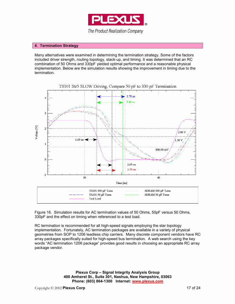
4. Termination Strategy Many alternatives were examined in determining the termination strategy. Some of the factors included driver strength, routing topology, stack-up, and timing. It was determined that an RC combination of 50 Ohms and 330pF yielded optimal performance and a reasonable physical implementation. Below are the simulation results showing the improvement in timing due to the termination.
Figure 16. Simulation results for AC termination values of 50 Ohms, 50pF versus 50 Ohms, 330pF and the effect on timing when referenced to a test load. RC termination is recommended for all high-speed signals employing the star topology implementation. Fortunately, AC termination packages are available in a variety of physical geometries from SOP to 1206 leadless chip carriers. Many discrete component vendors have RC array packages specifically suited for high-speed bus termination. A web search using the key words “AC termination 1206 package” provides good results in choosing an appropriate RC array package vendor.
Plexus Corp – Signal Integrity Analysis Group 400 Amherst St., Suite 301, Nashua, New Hampshire, 03063
Phone: (603) 864-1300 Internet: www.plexus.com
Copyright © 2002 Plexus Corp 18 of 24
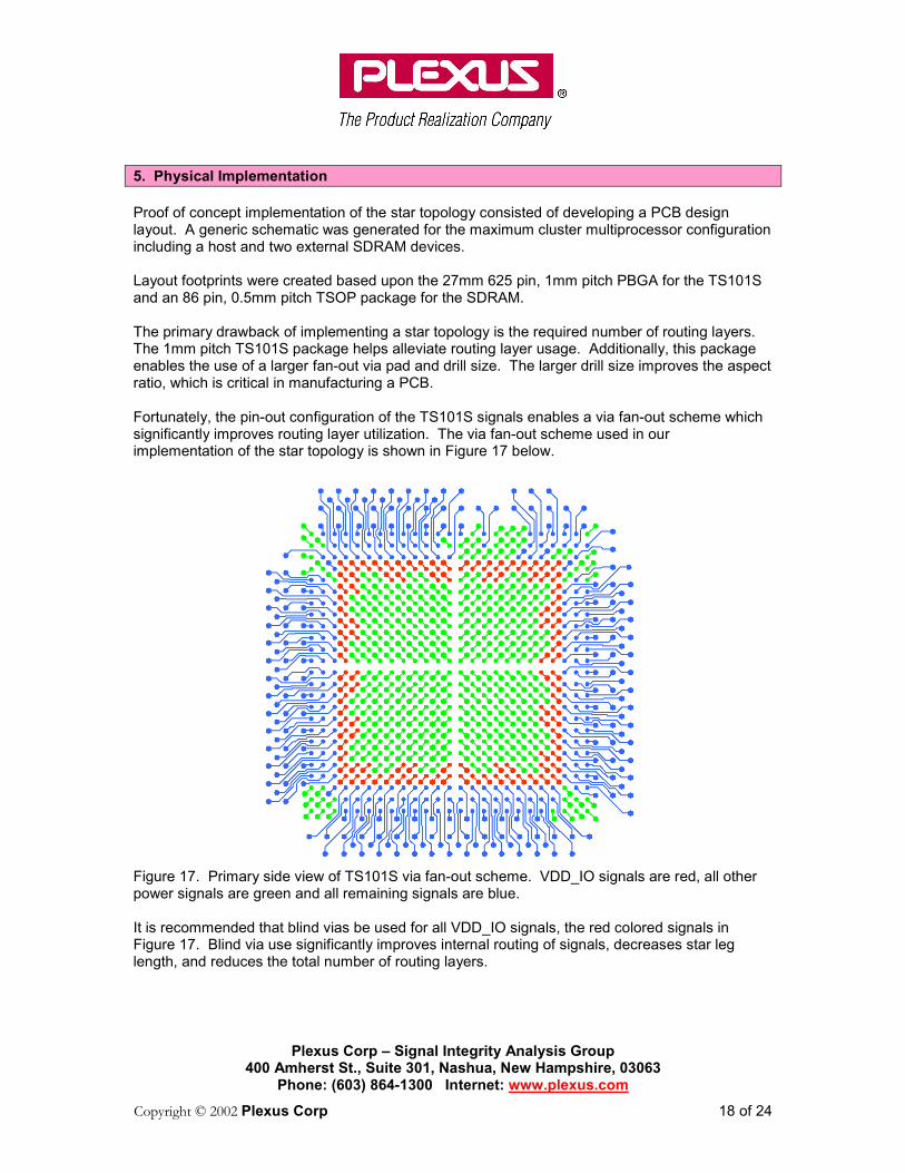
5. Physical Implementation Proof of concept implementation of the star topology consisted of developing a PCB design layout. A generic schematic was generated for the maximum cluster multiprocessor configuration including a host and two external SDRAM devices. Layout footprints were created based upon the 27mm 625 pin, 1mm pitch PBGA for the TS101S and an 86 pin, 0.5mm pitch TSOP package for the SDRAM. The primary drawback of implementing a star topology is the required number of routing layers. The 1mm pitch TS101S package helps alleviate routing layer usage. Additionally, this package enables the use of a larger fan-out via pad and drill size. The larger drill size improves the aspect ratio, which is critical in manufacturing a PCB. Fortunately, the pin-out configuration of the TS101S signals enables a via fan-out scheme which significantly improves routing layer utilization. The via fan-out scheme used in our implementation of the star topology is shown in Figure 17 below.
Figure 17. Primary side view of TS101S via fan-out scheme. VDD_IO signals are red, all other power signals are green and all remaining signals are blue. It is recommended that blind vias be used for all VDD_IO signals, the red colored signals in Figure 17. Blind via use significantly improves internal routing of signals, decreases star leg length, and reduces the total number of routing layers.
Plexus Corp – Signal Integrity Analysis Group 400 Amherst St., Suite 301, Nashua, New Hampshire, 03063
Phone: (603) 864-1300 Internet: www.plexus.com
Copyright © 2002 Plexus Corp 19 of 24
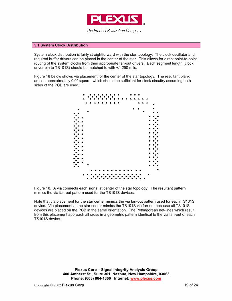
5.1 System Clock Distribution System clock distribution is fairly straightforward with the star topology. The clock oscillator and required buffer drivers can be placed in the center of the star. This allows for direct point-to-point routing of the system clocks from their appropriate fan-out drivers. Each segment length (clock driver pin to TS101S) should be matched to with +/- 250 mils. Figure 18 below shows via placement for the center of the star topology. The resultant blank area is approximately 0.9” square, which should be sufficient for clock circuitry assuming both sides of the PCB are used.
Figure 18. A via connects each signal at center of the star topology. The resultant pattern mimics the via fan-out pattern used for the TS101S devices. Note that via placement for the star center mimics the via fan-out pattern used for each TS101S device. Via placement at the star center mimics the TS101S via fan-out because all TS101S devices are placed on the PCB in the same orientation. The Pythagorean net-lines which result from this placement approach all cross in a geometric pattern identical to the via fan-out of each TS101S device.
Plexus Corp – Signal Integrity Analysis Group 400 Amherst St., Suite 301, Nashua, New Hampshire, 03063
Phone: (603) 864-1300 Internet: www.plexus.com
Copyright © 2002 Plexus Corp 20 of 24
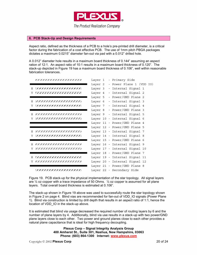
6. PCB Stack-Up and Design Requirements Aspect ratio, defined as the thickness of a PCB to a hole’s pre-printed drill diameter, is a critical factor during the fabrication of a cost effective PCB. The use of 1mm pitch PBGA packages dictates a maximum 0.0215” diameter fan-out via pad with a 0.012” drilled hole. A 0.012” diameter hole results in a maximum board thickness of 0.144” assuming an aspect ration of 12:1. An aspect ratio of 10:1 results in a maximum board thickness of 0.120”. The stack-up depicted in Figure 19 has a maximum board thickness of 0.106”, well within reasonable fabrication tolerances.
Layer 1 - Primary Side
Layer 3 - Internal Signal 1
Layer 4 - Internal Signal 2
Layer 2 - Power Plane 1 (VDD IO)
Layer 6 - Internal Signal 3
Layer 7 - Internal Signal 4
Layer 5 - Power/GND Plane 2
Layer 9 - Internal Signal 5
Layer 10 - Internal Signal 6
Layer 8 - Power/GND Plane 3
Layer 11 - Power/GND Plane 4
Layer 12 - Power/GND Plane 5
Layer 13 - Internal Signal 7
Layer 14 - Internal Signal 8
Layer 15 - Power/GND Plane 6
Layer 16 - Internal Signal 9
Layer 17 - Internal Signal 10
Layer 18 - Power/GND Plane 7
Layer 19 - Internal Signal 11
Layer 20 - Internal Signal 12
Layer 21 - Power/GND Plane 8
Layer 22 - Secondary Side
H
V
H
V
H
V
H
V
H
V
H
V
Figure 19. PCB stack-up for the physical implementation of the star topology. All signal layers are ½ oz copper with a trace impedance of 50 Ohms. ½ oz copper is assumed for all plane layers. Total overall board thickness is estimated at 0.106”. The stack-up shown in Figure 19 above was used to successfully route the star topology shown in Figure 2 on page 4. Blind vias are recommended for fan-out of VDD_IO signals (Power Plane 1). Blind via construction is limited by drill depth that results in an aspect ratio of 1:1, hence the location of VDD_IO in the stack-up above. It is estimated that blind via usage decreased the required number of routing layers by 6 and the number of plane layers by 4. Additionally, blind via use results in a stack-up with two power/GND plane layers close to each other. Two power and ground planes close to each other provides a natural plane capacitance that is ideal for high frequency decoupling.
Plexus Corp – Signal Integrity Analysis Group 400 Amherst St., Suite 301, Nashua, New Hampshire, 03063
Phone: (603) 864-1300 Internet: www.plexus.com
Copyright © 2002 Plexus Corp 21 of 24
The stack-up shown in Figure 19 can be modified for the addition of four more routing layers and 2 plane layers while maintaining the power/ground plane pairs. The addition of these layers will require an aspect ration of 12:1, however, there are several fabrication vendors that can successfully fabricate a PCB to this design requirement. Fabrication tolerances and capabilities vary significantly from any one vendor to another. Plexus’s design approach to this PCB was based on close collaboration with Marcel Electronics International of Orange, CA. Their input and capabilities help drive the PCB design requirements. It is highly recommended that PCB design engineer works closely with their fabrication vendor in order to determine feasibility of the design constraints outlined in this section.
Plexus Corp – Signal Integrity Analysis Group 400 Amherst St., Suite 301, Nashua, New Hampshire, 03063
Phone: (603) 864-1300 Internet: www.plexus.com
Copyright © 2002 Plexus Corp 22 of 24
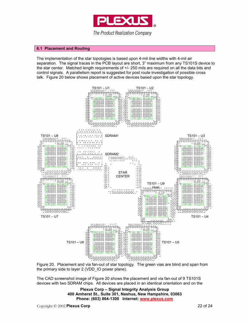
6.1 Placement and Routing The implementation of the star topologies is based upon 4-mil line widths with 4-mil air separation. The signal traces in the PCB layout are short, 3” maximum from any TS101S device to the star center. Matched length requirements of +/- 250 mils are required on all the data bits and control signals. A parallelism report is suggested for post route investigation of possible cross talk. Figure 20 below shows placement of active devices based upon the star topology.
Figure 20. Placement and via fan-out of star topology. The green vias are blind and span from the primary side to layer 2 (VDD_IO power plane). The CAD screenshot image of Figure 20 shows the placement and via fan-out of 9 TS101S devices with two SDRAM chips. All devices are placed in an identical orientation and on the
TS101 – U1 TS101 – U2
TS101 – U3
TS101 – U4
TS101 – U5 TS101 – U6
TS101 – U7
TS101 – U8
TS101 – U9Host
STAR CENTER
SDRAM1
SDRAM2
Plexus Corp – Signal Integrity Analysis Group 400 Amherst St., Suite 301, Nashua, New Hampshire, 03063
Phone: (603) 864-1300 Internet: www.plexus.com
Copyright © 2002 Plexus Corp 23 of 24
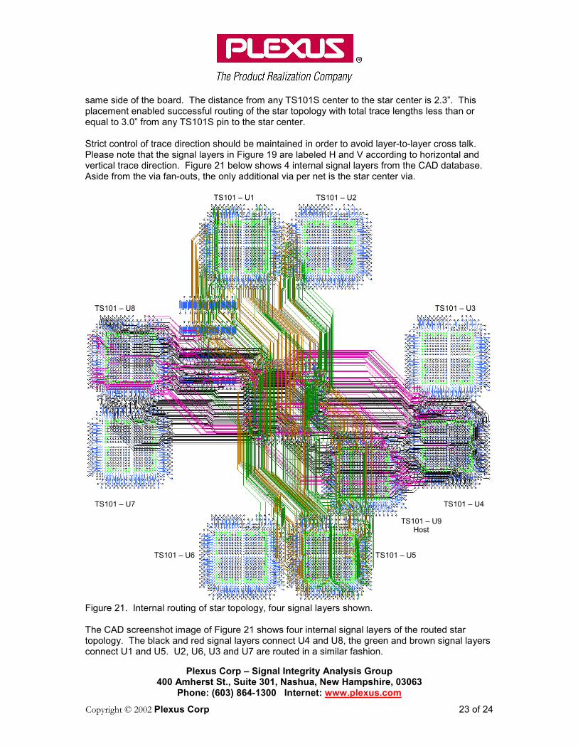
same side of the board. The distance from any TS101S center to the star center is 2.3”. This placement enabled successful routing of the star topology with total trace lengths less than or equal to 3.0” from any TS101S pin to the star center. Strict control of trace direction should be maintained in order to avoid layer-to-layer cross talk. Please note that the signal layers in Figure 19 are labeled H and V according to horizontal and vertical trace direction. Figure 21 below shows 4 internal signal layers from the CAD database. Aside from the via fan-outs, the only additional via per net is the star center via.
Figure 21. Internal routing of star topology, four signal layers shown. The CAD screenshot image of Figure 21 shows four internal signal layers of the routed star topology. The black and red signal layers connect U4 and U8, the green and brown signal layers connect U1 and U5. U2, U6, U3 and U7 are routed in a similar fashion.
TS101 – U1 TS101 – U2
TS101 – U3
TS101 – U4
TS101 – U5 TS101 – U6
TS101 – U7
TS101 – U8
TS101 – U9 Host
Plexus Corp – Signal Integrity Analysis Group 400 Amherst St., Suite 301, Nashua, New Hampshire, 03063
Phone: (603) 864-1300 Internet: www.plexus.com
Copyright © 2002 Plexus Corp 24 of 24
7. Conclusion The signal integrity analysis and design rules outlined in this document were developed to meet specific system requirements. The design goal was implementation of a reliable bus topology for 8 clustered TigerSHARCs (ADSP-TS101S) plus a host and external SDRAM with reliable operation at 100 MHz. Signal integrity and timing analysis showed that the recommended topology theoretically meets the design goal. Successful physical implementation of the recommended topology, based upon manufacturable design rules, provides a high degree of confidence that theoretical results can be achieved in the real world. About PLEXUSPlexus Corp. Headquartered in Neenah, Wisconsin, Plexus provides product realization services to original equipment manufacturers (OEMs) in the networking/datacommunications, medical, industrial and computer electronics industries. The Company offers engineering and product development including signal integrity analysis, new product introduction (NPI), prototyping, material procurement and management, assembly, testing, manufacturing, complex final system assembly, fulfillment and sustaining services. Further information about Plexus can be found on its website at www.plexus.com.