Embed Size (px)
Citation preview

ADSP-21262 EZ-KIT Lite®
Evaluation System Manual
Revision 1.2, March 2004
Part Number82-000800-01
Analog Devices, Inc.One Technology WayNorwood, Mass. 02062-9106 a

Copyright Information© 2004 Analog Devices, Inc., ALL RIGHTS RESERVED. This docu-ment may not be reproduced in any form without prior, express written consent from Analog Devices, Inc.
Printed in the USA.
Limited WarrantyThe EZ-KIT Lite evaluation system is warranted against defects in materi-als and workmanship for a period of one year from the date of purchase from Analog Devices or from an authorized dealer.
DisclaimerAnalog Devices, Inc. reserves the right to change this product without prior notice. Information furnished by Analog Devices is believed to be accurate and reliable. However, no responsibility is assumed by Analog Devices for its use; nor for any infringement of patents or other rights of third parties which may result from its use. No license is granted by impli-cation or otherwise under the patent rights of Analog Devices, Inc.
Trademark and Service Mark NoticeThe Analog Devices logo, VisualDSP++, the VisualDSP++ logo, SHARC, SHARC logo, CROSSCORE, the CROSSCORE logo, and EZ-KIT Lite are registered trademarks of Analog Devices, Inc.
All other brand and product names are trademarks or service marks of their respective owners.

Regulatory Compliance The ADSP-21262 EZ-KIT Lite evaluation system has been certified to comply with the essential requirements of the European EMC directive 89/336/EEC (inclusive 93/68/EEC) and, therefore, carries the “CE” mark.
The ADSP-21262 EZ-KIT Lite evaluation system had been appended to the Technical Construction File referenced “DSPTOOLS1” dated December 21, 1997 and was awarded CE Certification by an appointed European Competent Body as listed below.
Technical Certificate No: Z600ANA1.013
Issued by: Technology International (Europe) Limited
41 Shrivenham Hundred Business Park
Shrivenham, Swindon, SN6 8TZ, UK
The EZ-KIT Lite evaluation system contains ESD (electrostatic discharge) sensitive devices. Electro-static charges readily accumulate on the human body and equipment and can discharge without detection. Permanent damage may occur on devices subjected to high-energy discharges. Proper ESD precautions are recommended to avoid performance degradation or loss of functionality. Store unused EZ-KIT Lite boards in the protective shipping package.

CONTENTS
iv ADSP-21262 EZ-KIT Lite Evaluation System Manual
CONTENTS
PREFACE
Purpose of This Manual ................................................................. xiv
Intended Audience ......................................................................... xiv
Manual Contents ............................................................................ xv
What’s New in This Manual ............................................................ xv
Technical or Customer Support ...................................................... xvi
Supported Processors ...................................................................... xvi
Product Information ...................................................................... xvi
MyAnalog.com ........................................................................ xvii
DSP Product Information ........................................................ xvii
Related Documents ................................................................ xviii
Online Documentation ............................................................ xix
Printed Manuals ....................................................................... xix
VisualDSP++ Documentation Set ......................................... xix
Hardware Manuals ................................................................ xx
Data Sheets ........................................................................... xx
Contacting DSP Publications ..................................................... xx
Notation Conventions .................................................................... xxi
ADSP-21262 EZ-KIT Lite Evaluation System Manual v

CONTENTS
GETTING STARTED
Contents of EZ-KIT Lite Package ................................................. 1-1
PC Configuration ......................................................................... 1-3
Installation Tasks .......................................................................... 1-3
Installing VisualDSP++ and EZ-KIT Lite Software .................. 1-4
Installing and Registering VisualDSP++ License ....................... 1-4
Setting Up EZ-KIT Lite Hardware .......................................... 1-5
Installing EZ-KIT Lite USB Driver ......................................... 1-7
Windows 98 USB Driver .................................................... 1-8
Windows 2000 USB Driver .............................................. 1-12
Windows XP USB Driver ................................................. 1-13
Verifying Driver Installation .................................................. 1-15
Starting VisualDSP++ ........................................................... 1-16
USING EZ-KIT LITE
EZ-KIT Lite License Restrictions .................................................. 2-2
Using External Memory ................................................................ 2-2
Using Analog Audio ...................................................................... 2-3
Using Digital Audio ...................................................................... 2-5
Using LEDs and Push Buttons ...................................................... 2-6
Example Programs ........................................................................ 2-7
Background Telemetry Channel .................................................... 2-8
Using EZ-KIT Lite VisualDSP++ Interface .................................... 2-8
Boot Load ............................................................................... 2-8
vi ADSP-21262 EZ-KIT Lite Evaluation System Manual

CONTENTS
Target Options ........................................................................ 2-9
While Target is Halted and On Emulator Exit Options ........ 2-9
Other Options .................................................................. 2-10
Core Hang Conditions .......................................................... 2-11
Hardware Breakpoints ........................................................... 2-12
Common Hardware Breakpoint Attributes ......................... 2-13
Global Hardware Breakpoint Options ................................ 2-14
Data Hardware Breakpoints ............................................... 2-14
Instruction Hardware Breakpoints ..................................... 2-15
Other Breakpoints ............................................................. 2-17
Tips and Tricks Using Hardware Breakpoints ..................... 2-18
Latency ......................................................................... 2-18
Restrictions ................................................................... 2-18
Setting a Breakpoint on a Single Address ........................ 2-18
EZ-KIT LITE HARDWARE REFERENCE
System Architecture ...................................................................... 3-2
Parallel Port ............................................................................. 3-3
DAI Interface .......................................................................... 3-4
SPI Interface ........................................................................... 3-6
FLAG Pins .............................................................................. 3-6
Expansion Interface ................................................................. 3-7
JTAG Emulation Port .............................................................. 3-7
DIP Switch Settings ...................................................................... 3-8
Electret Microphone Select Switch (SW6) ................................ 3-9
ADSP-21262 EZ-KIT Lite Evaluation System Manual vii
CONTENTS
Codec Setup Switch (SW7) ..................................................... 3-9
SPDIF Signal Enable Switch (SW8) ....................................... 3-10
Push Button Enable Switch (SW9) ........................................ 3-10
Boot Mode and Clock Ratio Select Switch (SW10) ................ 3-11
Loop-Back Test Switch (SW11) ............................................. 3-12
LEDs and Push Buttons .............................................................. 3-12
General Purpose LEDs (LED8–1) .......................................... 3-13
Reset LEDs (LED9, LED12) ................................................. 3-14
Power LED (LED10) ............................................................ 3-14
SPDIF GPO1 LED (LED11) ................................................ 3-14
USB Monitor LED (LED13) ................................................. 3-14
Push Buttons (SW4–1) .......................................................... 3-14
Board Reset Push Button (SW5) ............................................ 3-15
Connectors ................................................................................. 3-15
Expansion Interface (J1, J2, J3) ............................................. 3-15
Audio In RCA Connector (J4) ............................................... 3-17
Audio Out RCA Connector (J5) ............................................ 3-17
Headphone Out Jack (J6) ...................................................... 3-17
Power Jack (J7) ..................................................................... 3-17
SPDIF In Coax Connector (P1) ............................................ 3-18
SPI Header (P2) .................................................................... 3-18
DAI Header (P3) .................................................................. 3-18
USB Connector (P4) ............................................................. 3-19
JTAG Header (P5) ................................................................ 3-19
viii ADSP-21262 EZ-KIT Lite Evaluation System Manual

CONTENTS
BILL OF MATERIALS
INDEX
ix ADSP-21262 EZ-KIT Lite Evaluation System Manual

CONTENTS
x ADSP-21262 EZ-KIT Lite Evaluation System Manual

PREFACE
Thank you for purchasing the ADSP-21262 EZ-KIT Lite®, Analog
Devices (ADI) evaluation system for SHARC® processors.The SHARC processors are based on a 32-bit super Harvard architecture that includes a unique memory architecture comprised of two large on-chip, dual-ported SRAM blocks coupled with a sophisticated IO pro-cessor, which gives SHARC the bandwidth for sustained high-speed computations. SHARC represents today’s de facto standard for float-ing-point DSP targeted for premium audio applications.
The evaluation system is designed to be used in conjunction with the VisualDSP++® development environment to test the capabilities of the ADSP-21262 SHARC processors. The VisualDSP++ development envi-ronment gives you the ability to perform advanced application code development and debug, such as:
• Create, compile, assemble, and link application programs written in C++, C, and ADSP-21262 assembly
• Load, run, step, halt, and set breakpoints in application program
• Read and write data and program memory
• Read and write core and peripheral registers
• Plot memory
Access to the ADSP-21262 processor from a personal computer (PC) is achieved through a USB port or an optional JTAG emulator. The USB interface gives unrestricted access to the ADSP-21262 processor and the
ADSP-21262 EZ-KIT Lite Evaluation System Manual xi

evaluation board peripherals. Analog Devices JTAG emulators offer faster communication between the host PC and target hardware. Analog Devices carries a wide range of in-circuit emulation products. To learn more about Analog Devices emulators and DSP development tools, go to http://www.analog.com/dsp/tools/.
ADSP-21262 EZ-KIT Lite provides example programs to demonstrate the capabilities of the evaluation board.
The VisualDSP++ license provided with this EZ-KIT Lite evalua-tion system limits the size of a user program’s code to 10922 words of program memory.
The board features:
• Analog Devices ADSP-21262 processor
136-pin BGA package300 MHz Core Clock Speed
• Synchronous Read Access Memory (SRAM)
512 Kbit x 8-bit
• Flash Memory
1M x 8-bit
• Serial Peripheral Interconnect (SPI) Flash Memory
512 Kbit
• Analog Audio Interface
AD1835A codec 4x2 RCA phono jack for 4 channels of stereo output2x1 RCA phono jack for 1 channel of stereo inputHeadphone jack for 1 channel stereo output
xii ADSP-21262 EZ-KIT Lite Evaluation System Manual

Preface
• Digital Audio Interface
CS8416 SPDIF receiver RCA phono jack input
• LEDs
12 LEDs: 1 power (green), 1 board reset (red), 1 USB reset (red), 1 USB monitor (amber), and 8 general purpose (amber)
• Push Buttons
5 push buttons: 1 reset, 2 connected to DAI, 2 connected to DSP FLAG pins
• Expansion Interface (Type A)
Parallel Port, FLAGs, DAI, SPI
• Other Features
JTAG ICE 14-pin header0-ohm resistors for DSP current measurementSPI headerDAI header
The EZ-KIT Lite board has a total of 1 MB of parallel Flash memory and 512 Kbit of SPI Flash memory. The Flash memories can store user-spe-cific boot code, allowing the board to run as a stand-alone unit. For more information, see “Using External Memory” on page 2-2 and “Boot Mode and Clock Ratio Select Switch (SW10)” on page 3-11. The board also has 512 KB of SRAM, which can be used at runtime.
The DAI of the DSP connects to the AD1835A audio codec and the CS8416 SPDIF receiver. These devices allow you to create digital and ana-log audio signal processing applications. See “Using Analog Audio” on page 2-3 and “Using Digital Audio” on page 2-5 for more information.
ADSP-21262 EZ-KIT Lite Evaluation System Manual xiii

Purpose of This Manual
Additionally, the EZ-KIT Lite board provides access to all of the proces-sor’s peripheral ports. Access is provided in the form of a three-connector expansion interface. See “Expansion Interface” on page 3-7 for details.
Purpose of This Manual The ADSP-21262 EZ-KIT Lite Evaluation System Manual provides instructions for using the hardware and installing the software on your PC. The text includes guidelines for running your own code on the ADSP-21262 EZ-KIT Lite. The manual also describes the board’s config-uration and components. Finally, a schematic and a bill of materials are provided as a reference for future ADSP-21262 board designs.
Intended AudienceThis manual is a user’s guide and reference to the ADSP-21262 EZ-KIT Lite evaluation system. Programmers who are familiar with the Analog Devices SHARC processor architecture, operation, and programming are the primary audience for this manual.
Programmers who are unfamiliar with Analog Devices SHARC processors can use this manual in conjunction with the ADSP-2126x SHARC Core Reference and ADSP-21262/21266 Peripherals Manual and the ADSP-21160 SHARC DSP Instruction Set Reference, which describe the DSP’a architecture and instruction set. Programmers who are unfamiliar with VisualDSP++ should refer to the VisualDSP++ online Help and the VisualDSP++ user’s or getting started guides. For the locations of these documents, see “Related Documents” on page -xviii.
xiv ADSP-21262 EZ-KIT Lite Evaluation System Manual

Preface
Manual ContentsThe manual consists of:
• Chapter 2, “Getting Started” on page 1-1Provides software and hardware installation procedures, PC system requirements, and basic board information.
• Chapter 2, “Using EZ-KIT Lite” on page 2-1Provides information on the EZ-KIT Lite from a programmer’s perspective and provides an easy-to-access memory map.
• Chapter 3, “EZ-KIT Lite Hardware Reference” on page 3-1Provides information on the hardware aspects of the evaluation system.
• Appendix A, “Bill Of Materials” on page A-1Provides a list of components used to manufacture the EZ-KIT Lite board.
• Appendix B, “Schematics” on page B-1Provides the resources to allow modifications to the EZ-KIT Lite or to use as a reference design.This appendix is not part of the online Help. The online Help viewers should go the PDF version of the ADSP-21262 EZ-KIT Lite Evaluation System Manual located in the Docs\EZ-KIT Lite Manuals folder on the installation CD to see the schematics.
What’s New in This Manual This edition of the ADSP-21262 EZ-KIT Lite Evaluation System Manual includes the updated installation and license registration procedures.
ADSP-21262 EZ-KIT Lite Evaluation System Manual xv

Technical or Customer Support
Technical or Customer SupportYou can reach DSP Tools Support in the following ways.
• Visit the DSP Development Tools website at
www.analog.com/technology/dsp/developmentTools/index.html
• Email questions to
• Phone questions to 1-800-ANALOGD
• Contact your ADI local sales office or authorized distributor
• Send questions by mail to
Analog Devices, Inc.
One Technology Way
P.O. Box 9106
Norwood, MA 02062-9106
USA
Supported ProcessorsThe ADSP-21262 EZ-KIT Lite evaluation system supports Analog Devices ADSP-21262 SHARC DSPs.
Product InformationYou can obtain product information from the Analog Devices website, from the product CD-ROM, or from the printed publications (manuals).
xvi ADSP-21262 EZ-KIT Lite Evaluation System Manual

Preface
Analog Devices is online at www.analog.com. Our website provides infor-mation about a broad range of products—analog integrated circuits, amplifiers, converters, and digital signal processors.
MyAnalog.comMyAnalog.com is a free feature of the Analog Devices website that allows customization of a webpage to display only the latest information on products you are interested in. You can also choose to receive weekly email notification containing updates to the webpages that meet your interests. MyAnalog.com provides access to books, application notes, data sheets, code examples, and more.
Registration:
Visit www.myanalog.com to sign up. Click Register to use MyAnalog.com. Registration takes about five minutes and serves as means for you to select the information you want to receive.
If you are already a registered user, just log on. Your user name is your email address.
DSP Product InformationFor information on digital signal processors, visit our website at www.analog.com/dsp, which provides access to technical publications, data sheets, application notes, product overviews, and product announcements.
You may also obtain additional information about Analog Devices and its products in any of the following ways.
• Email questions or requests for information to [email protected]
• Fax questions or requests for information to 1-781-461-3010 (North America) or +49 (0) 89 76903-157 (Europe)
ADSP-21262 EZ-KIT Lite Evaluation System Manual xvii

Product Information
Related DocumentsFor information on product related development software, see the follow-ing publications.
Table 1. Related DSP Publications
Title Description
ADSP-21262 SHARC Microprocessor Datasheet General functional description, pinout, and timing
ADSP-2126x SHARC DSP Core ManualADSP-2126x SHARC DSP Peripherals Manual
Description of internal processor architecture, registers, and all peripheral functions
ADSP-21160 SHARC DSP Instruction Set Ref-erence
Description of all allowed processor assembly instructions
Table 2. Related VisualDSP++ Publications
VisualDSP++ 3.5 User’s Guide for 32-Bit Processors
Detailed description of VisualDSP++ 3.5 features and usage
VisualDSP++ 3.5 Assembler and Preprocessor Manual for SHARC Processors
Description of the assembler function and commands for SHARC processors
VisualDSP++ 3.5 C/C++ Complier and Library Manual for SHARC Processors
Description of the complier function and com-mands for SHARC processors
VisualDSP++ 3.5 Linker and Utilities Manual for 32-Bit Processors
Description of the linker function and com-mands for the 32-bit processors
VisualDSP++ 3.5 Loader Manual for 32-Bit Processors
Description of the loader function and com-mands for the 32-bit processors
VisualDSP++ 3.5 User’s Guide for 32-Bit Proces-sors
Detailed description of VisualDSP++ 3.5 fea-tures and usage
xviii ADSP-21262 EZ-KIT Lite Evaluation System Manual
Preface
The listed documents can be found through online Help or in the Docs folder of your VisualDSP++ installation. Most documents are available in printed form.
If you plan to use the EZ-KIT Lite board in conjunction with a JTAG emulator, refer to the documentation that accompanies the emulator.
Online Documentation Your software installation kit includes online Help as part of the Win-dows® interface. These help files provide information about VisualDSP++ and the ADSP-21262 EZ-KIT Lite evaluation system.
To view VisualDSP++ Help, click on the Help menu item or go to the Windows task bar and select Start –>Programs –>Analog Devices–>Visu-alDSP++ for 32-bit Processors –>VisualDSP++ Documentation.
To view ADSP-21262 EZ-KIT Lite Help, which now is a part of the Visu-alDSP++ Help system, go the Contents tab of the Help window and select Manuals –>Hardware Tools –>EZ-KIT Lite Evaluation Systems.
For more documentation, please go to http://www.analog.com/technology/dsp/library.html.
Printed ManualsFor general questions regarding literature ordering, call the Literature Center at 1-800-ANALOGD (1-800-262-5643) and follow the prompts.
VisualDSP++ Documentation Set
Printed copies of VisualDSP++ manuals may be purchased through Ana-log Devices Customer Service at 1-781-329-4700; ask for a Customer Service representative. The manuals can be purchased only as a kit. For additional information, call 1-603-883-2430.
ADSP-21262 EZ-KIT Lite Evaluation System Manual xix

Product Information
If you do not have an account with Analog Devices, you will be referred to Analog Devices distributors. To get information on our distributors, log onto www.analog.com/salesdir/continent.asp.
Hardware Manuals
Printed copies of hardware reference and instruction set reference manuals can be ordered through the Literature Center or downloaded from the Analog Devices website. The phone number is 1-800-ANALOGD (1-800-262-5643). The manuals can be ordered by a title or by product number located on the back cover of each manual.
Data Sheets
All data sheets can be downloaded from the Analog Devices website. As a general rule, printed copies of data sheets with a letter suffix (L, M, N, S) can be obtained from the Literature Center at 1-800-ANALOGD (1-800-262-5643) or downloaded from the website. Data sheets without the suffix can be downloaded from the website only—no hard copies are available. You can ask for the data sheet by part name or by product number.
If you want to have a data sheet faxed to you, the phone number for that service is 1-800-446-6212. Follow the prompts and a list of data sheet code numbers will be faxed to you. Call the Literature Center first to find out if requested data sheets are available.
Contacting DSP PublicationsPlease send your comments and recommendations on how to improve our manuals and online Help. You can contact us at [email protected].
xx ADSP-21262 EZ-KIT Lite Evaluation System Manual

Preface
Notation ConventionsThe following table identifies and describes text conventions used in this manual.
Additional conventions, which apply only to specific chapters, may appear throughout this document.
Example Description
Close command (File menu) or OK
Text in bold style indicates the location of an item within the VisualDSP++ environment’s and boards’ menu system and user interface items.
{this | that} Alternative required items in syntax descriptions appear within curly brackets separated by vertical bars; read the example as this or that.
[this | that] Optional items in syntax descriptions appear within brackets and sepa-rated by vertical bars; read the example as an optional this or that.
[this,…] Optional item lists in syntax descriptions appear within brackets delim-ited by commas and terminated with an ellipsis; read the example as an optional comma-separated list of this.
PF9–0 Registers, connectors, pins, commands, directives, keywords, code exam-ples, and feature names are in text with letter gothic font.
filename Non-keyword placeholders appear in text with italic style format.
Note: A note providing information of special interest or identifying a related topic. In the online version of this book, the word Note appears instead of this symbol.
Caution: A caution providing information about critical design or programming issues that influence operation of a product. In the online version of this book, the word Caution appears instead of this symbol.
ADSP-21262 EZ-KIT Lite Evaluation System Manual xxi

Notation Conventions
xxii ADSP-21262 EZ-KIT Lite Evaluation System Manual

1 GETTING STARTED
This chapter provides the information you need to begin using
ADSP-21262 EZ-KIT Lite evaluation system. For correct operation, install the software and hardware in the order presented in “Installation Tasks” on page 1-3.The chapter includes the following sections.
• “Contents of EZ-KIT Lite Package” on page 1-1Provides a list of the components shipped with this EZ-KIT Lite evaluation system.
• “PC Configuration” on page 1-3Describes the minimum requirements for the PC to work with the EZ-KIT Lite evaluation system.
• “Installation Tasks” on page 1-3Describes the step-by-step procedures for setting up the hardware and software.
Contents of EZ-KIT Lite PackageYour ADSP-21262 EZ-KIT Lite evaluation system package contains the following items.
• ADSP-21262 EZ-KIT Lite board
• EZ-KIT Lite Installation Procedure
ADSP-21262 EZ-KIT Lite Evaluation System Manual 1-1

Contents of EZ-KIT Lite Package
• CD containing:
VisualDSP++ 3.5 for 32-bit processors with a limited license
ADSP-21262 EZ-KIT Lite debug software
USB driver files
Example programs
ADSP-21262 EZ-KIT Lite Evaluation System Manual (this document)
• VisualDSP++ 3.5 Installation Quick Reference Card
• Universal 7.5V DC power supply
• USB 2.0 type cable
• Registration card (please fill out and return)
If any item is missing, contact the vendor where you purchased your EZ-KIT Lite or contact Analog Devices, Inc.
The EZ-KIT Lite evaluation system contains ESD (electrostatic discharge) sensitive devices. Electro-static charges readily accumulate on the human body and equipment and can discharge without detection. Permanent damage may occur on devices subjected to high-energy discharges. Proper ESD precautions are recommended to avoid performance degradation or loss of functionality. Store unused EZ-KIT Lite boards in the protective shipping package.
1-2 ADSP-21262 EZ-KIT Lite Evaluation System Manual

Getting Started
PC ConfigurationFor correct operation of the VisualDSP++ software and the EZ-KIT Lite, your computer must have the minimum configuration:
EZ-KIT Lite does not run under Windows 95 or Windows NT.
Installation TasksThe following task list is provided for the safe and effective use of the ADSP-21262 EZ-KIT Lite. Follow the instructions in the presented order to ensure correct operation of your software and hardware.
1. VisualDSP++ and EZ-KIT Lite software installation
2. VisualDSP++ license installation and registration
3. EZ-KIT Lite hardware setup
4. EZ-KIT Lite USB driver installation
5. USB driver installation verification
6. VisualDSP++ startup
Windows 98, Windows 2000, Windows XP
Intel (or comparable) 166MHz processor
VGA Monitor and color video card
2-button mouse
50 MB free on hard drive
32 MB RAM
Full-speed USB port
CD-ROM Drive
ADSP-21262 EZ-KIT Lite Evaluation System Manual 1-3

Installation Tasks
Installing VisualDSP++ and EZ-KIT Lite SoftwareThis EZ-KIT Lite comes with the latest version of VisualDSP++ 3.5 for 32-bit processors. VisualDSP++ installation includes EZ-KIT Lite installations.
To install VisualDSP++ and EZ-KIT Lite software:
1. Insert the VisualDSP++ installation CD into the CD-ROM drive.
2. If Autoplay is enabled on your PC, you see the Install Shield Wiz-ard Welcome screen. Otherwise, choose Run from the Start menu, and enter D:\ADI_Setup.exe in the Open field, where D is the name of your local CD-ROM drive.
3. Follow the on-screen instructions to continue installing the software.
4. At the Custom Setup screen, select your EZ-KIT Lite from the list of available systems and choose the installation directory. Click an icon in the Feature Description field to see the selected system’s description. When you have finished, click Next.
5. At the Ready to Install screen, click Back to change your install options, click Install to install the software, or click Cancel to exit the install.
6. When the EZ-KIT Lite installs, the Wizard Completed screen appears. Click Finish.
Installing and Registering VisualDSP++ LicenseVisualDSP++ and EZ-KIT Lites are licensed products. You may run only one copy of the software for each license purchased. Once a new copy of the VisualDSP++ or EZ-KIT Lite software is installed on your PC, you must install, register, and validate your licence.
1-4 ADSP-21262 EZ-KIT Lite Evaluation System Manual

Getting Started
The VisualDSP++ 3.5 Installation Quick Reference Card included in your package will guide you through the licence installation and registration process (refer to Tasks 1, 2, and 3).
Setting Up EZ-KIT Lite Hardware
The ADSP-21262 EZ-KIT Lite board is designed to run outside your per-sonal computer as a stand-alone unit. You do not have to open your computer case.
To connect the EZ-KIT Lite board:
1. Remove the EZ-KIT Lite board from the package. Be careful when handling the board to avoid the discharge of static electricity, which may damage some components.
2. Figure 1-1 shows the default jumper settings, DIP switch, connec-tor locations, and LEDs used in installation. Confirm that your board is set up in the default configuration before continuing.
The EZ-KIT Lite evaluation system contains ESD (electrostatic discharge) sensitive devices. Electrostatic charges readily accumulate on the human body and equipment and can discharge without detection. Per-manent damage may occur on devices subjected to high-energy discharges. Proper ESD precautions are recommended to avoid performance degradation or loss of functionality. Store unused EZ-KIT Lite boards in the protective shipping package.
ADSP-21262 EZ-KIT Lite Evaluation System Manual 1-5

Installation Tasks
3. Plug the provided power supply into J7 on the EZ-KIT Lite board. Visually verify that the green power LED (LED10) is on. Also verify that the two red reset LEDs (LED9 and LED12) go on for a moment and then go off, and, finally, LED8–1 are continually blinking.
4. Connect one end of the USB cable to an available full speed USB port on your PC and the other end to P4 on the ADSP-21262 EZ-KIT Lite board.
Figure 1-1. EZ-KIT Lite Hardware Setup
1-6 ADSP-21262 EZ-KIT Lite Evaluation System Manual

Getting Started
Installing EZ-KIT Lite USB DriverThe EZ-KIT Lite evaluation system installed on the following platforms requires one full-speed USB port.
• “Windows 98 USB Driver” on page 1-8 describes the installation on Windows 98.
• “Windows 2000 USB Driver” on page 1-12 describes the installa-tion on Windows 2000.
• “Windows XP USB Driver” on page 1-13 describes the installation on Windows XP.
The USB driver used by the debug agent is not Microsoft certified because it is intended for a development or laboratory environment, not a com-mercial environment.
ADSP-21262 EZ-KIT Lite Evaluation System Manual 1-7

Installation Tasks
Windows 98 USB Driver
Before using the ADSP-21262 EZ-KIT Lite for the first time, the Win-dows 98 USB driver must first be installed.
To install the USB driver:
1. Insert the CD into the CD-ROM drive.The connection of the device to the USB port activates the Win-dows 98 Add New Hardware Wizard shown in Figure 1-2.
2. Click Next.
Figure 1-2. Windows 98 – Add New Hardware Wizard
1-8 ADSP-21262 EZ-KIT Lite Evaluation System Manual

Getting Started
3. Select Search for the best driver for your device, as shown in Figure 1-3.
4. Click Next.
5. Select CD-ROM drive, as shown in Figure 1-4.
Figure 1-3. Windows 98 – Searching for Driver
Figure 1-4. Windows 98 – Searching for CD-ROM
ADSP-21262 EZ-KIT Lite Evaluation System Manual 1-9

Installation Tasks
6. Click Next. Windows 98 locates the WmUSBEz.inf file on the installation CD, as shown in Figure 1-5.
7. Click Next.The Coping Files dialog box appears (Figure 1-6).
Figure 1-5. Windows 98 – Locating Driver
Figure 1-6. Windows 98 – Searching for .SYS File
1-10 ADSP-21262 EZ-KIT Lite Evaluation System Manual

Getting Started
8. Click Browse. The Open dialog box, shown in Figure 1-7, appears on the screen.
9. In Drives, select your CD-ROM drive.
10. Click OK. The Copying Files dialog box (Figure 1-8) appears.
Figure 1-7. Windows 98 – Opening .SYS File
Figure 1-8. Windows 98 – Copying .SYS File
ADSP-21262 EZ-KIT Lite Evaluation System Manual 1-11

Installation Tasks
11. Click OK.The driver installation is now complete, as shown in Figure 1-9.
12. Click Finish to exit the wizard.
Verify the installation by following the instructions in “Verifying Driver Installation” on page 1-15.
Windows 2000 USB Driver
VisualDSP++ 3.5 installation software pre-installs the necessary drivers for the selected EZ-KIT Lite. The install also upgrades an older driver if such is detected in the system.
Prior to running the VisualDSP++ 3.5 installer, ensure there are no other Hardware Wizard windows running in the background. If there are any wizard windows running, close them before starting the installer.
Figure 1-9. Windows 98 – Completing Software Installation
1-12 ADSP-21262 EZ-KIT Lite Evaluation System Manual

Getting Started
To install the USB driver:
1. If VisualDSP++ 3.5 is already installed on your system, go to step 2. Otherwise, run VisualDSP++ 3.5 installation. Refer to the VisualDSP++ 3.5 Installation Quick Reference Card for a detailed installation description. When installing VisualDSP++ 3.5 on Windows 2000, make sure the appropriate EZ-KIT Lite compo-nent is selected for the installation.
2. Connect the EZ-KIT Lite device to your PC’s USB port. Windows 2000 automatically detects an EZ-KIT device and auto-matically installs the appropriate driver for the selected device (see step 1).
3. Verify the installation by following the instructions in “Verifying Driver Installation” on page 1-15.
Windows XP USB Driver
VisualDSP++ 3.5 installation software pre-installs the necessary drivers for the selected EZ-KIT Lite. The install also upgrades an older driver if such is detected in the system.
Prior to running the VisualDSP++ 3.5 installer, ensure there are no other Hardware Wizard windows running in the background. If there are any wizard windows running, close them before starting the installer.
To install the USB driver:
1. If VisualDSP++ 3.5 is already installed on your system, go to step 2. Otherwise, run VisualDSP++ 3.5 installation. Refer to the VisualDSP++ 3.5 Installation Quick Reference Card for a detailed
ADSP-21262 EZ-KIT Lite Evaluation System Manual 1-13

Installation Tasks
installation description. When installing VisualDSP++ 3.5 on Windows XP, make sure the appropriate EZ-KIT Lite component is selected for the installation.
2. Connect the EZ-KIT Lite device to your PC’s USB port. By connecting the device to the USB port you activate the Win-dows XP Found New Hardware Wizard, shown in Figure 1-10.
3. Select Install the software automatically (Recommended) and click Next.
Figure 1-10. Windows XP – Found New Hardware Wizard
1-14 ADSP-21262 EZ-KIT Lite Evaluation System Manual

Getting Started
When Windows XP completes the driver installation for the selected device (see step 1), a window shown in Figure 1-11 appears on the screen.
4. Verify the installation by following the instructions in “Verifying Driver Installation”.
Verifying Driver InstallationBefore launching the EZ-KIT Lite evaluation system, verify that the USB driver software is installed properly:
1. Ensure that the USB cable connects to the evaluation board and the PC.
2. Verify that the yellow USB monitor LED (LED11) is lit. This signi-fies that the board is communicating properly with the host PC and is ready to run VisualDSP++.
Figure 1-11. Windows XP – Completing Driver Installation
ADSP-21262 EZ-KIT Lite Evaluation System Manual 1-15

Installation Tasks
3. Verify that the USB driver software is installed properly.
Open Windows Device Manager and verify that ADSP-21262 EZ-KIT Lite shows under DSP Emulators with no exclamation point, as in Figure 1-12.
If using an EZ-KIT Lite on Windows 98, disconnect the USB cable from the board before booting the PC. When Windows 98 is booted and you are logged on, re-connect the USB cable to the board. The operation should continue normally from this point.
Starting VisualDSP++To set up a session in VisualDSP++:
1. Verify that the yellow USB monitor LED (LED11, located near the USB connector) is lit. This signifies that the board is communicat-ing properly with the host PC and is ready to run VisualDSP++.
2. Press and hold down the keyboard Control (CTRL) key.
Figure 1-12. Device Manager Window
1-16 ADSP-21262 EZ-KIT Lite Evaluation System Manual
Getting Started
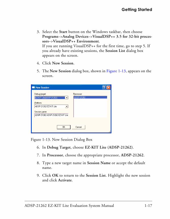
3. Select the Start button on the Windows taskbar, then choose Programs–>Analog Devices–>VisualDSP++ 3.5 for 32-bit proces-sors–>VisualDSP++ Environment.If you are running VisualDSP++ for the first time, go to step 5. If you already have existing sessions, the Session List dialog box appears on the screen.
4. Click New Session.
5. The New Session dialog box, shown in Figure 1-13, appears on the screen.
6. In Debug Target, choose EZ-KIT Lite (ADSP-21262).
7. In Processor, choose the appropriate processor, ADSP-21262.
8. Type a new target name in Session Name or accept the default name.
9. Click OK to return to the Session List. Highlight the new session and click Activate.
Figure 1-13. New Session Dialog Box
ADSP-21262 EZ-KIT Lite Evaluation System Manual 1-17

Installation Tasks
1-18 ADSP-21262 EZ-KIT Lite Evaluation System Manual

2 USING EZ-KIT LITE
This chapter provides specific information to assist you with developing
programs for the ADSP-21262 EZ-KIT Lite evaluation system. This information appears in the following sections.• “EZ-KIT Lite License Restrictions” on page 2-2Describes the restrictions of the VisualDSP++ license shipped with the EZ-KIT Lite.
• “Using External Memory” on page 2-2Describes how to access external memory and defines the memory map of the EZ-KIT Lite.
• “Using Analog Audio” on page 2-3·Describes how to set up and communicate with the on-board audio codec.
• “Using Digital Audio” on page 2-5Describes how to use the on-board SPDIF receiver.
• “Example Programs” on page 2-7Provides information about the example programs included in the ADSP-21262 EZ-KIT Lite evaluation system.
• “Background Telemetry Channel” on page 2-8Highlights the advantages of the Background Telemetry Channel feature of VisualDSP++.
ADSP-21262 EZ-KIT Lite Evaluation System Manual 2-1

EZ-KIT Lite License Restrictions
• “Using EZ-KIT Lite VisualDSP++ Interface” on page 2-8Describes the trace, performance monitoring, boot loading, context switching, and target options facilities of the EZ-KIT Lite system.
For detailed information on how to program the ADSP-21262 SHARC processor, refer to the documents referenced in “Related Documents”.
EZ-KIT Lite License RestrictionsThe license shipped with the EZ-KIT Lite imposes the following restrictions.
• The size of a user program’s code is limited to 10922 words of the ADSP-21262 processor’s program memory.
• No connections to Simulator or Emulator sessions are allowed.
• The EZ-KIT Lite hardware must be connected and powered up in order to use VisualDSP++ with a kit license.
Using External MemoryThe EZ-KIT Lite contains three types of memory: parallel Flash (1 MB), SPI Flash (512 Kbit) and SRAM (512 Kbit). The Flash memories can store user-specific boot code, letting the board to run as a stand-alone unit. For more information about setting the boot device for the DSP, see “Boot Mode and Clock Ratio Select Switch (SW10)” on page 3-11.
Table 2-1 provides a map of the board’s external memory.
The parallel Flash memory and the SRAM connect to the parallel port of the DSP. The parallel port is a multiplexed address and data port. The port can connect to 8-bit and 16-bit memory devices. When configuring the parallel port, keep in mind that the memory devices on the board are 8 bits wide.
2-2 ADSP-21262 EZ-KIT Lite Evaluation System Manual

Using EZ-KIT Lite
To access the SRAM and Flash memories, set up a Parallel Port DMA. For more information on how to connect the SRAM and Flash memories, see “Parallel Port” on page 3-3.
The SPI Flash memory connects to the DSP’s SPI port and uses Flag0 as a chip select. In order for FLAG0 to behave as a chip select, clear the PPFLG bit in the SYSCLT register.
An example program is included in the EZ-KIT installation directory to demonstrate how the parallel port and SPI port can be configured to access the memories.
Using Analog AudioThe AD1835A is a high-performance, single-chip codec featuring four ste-reo digital-to-analog converters (DAC) for audio output and one stereo analog-to-digital converters (ADC) for audio input. The codec can input and output data with a sample rate of up to 96 kHz on all channels. A 192 kHz sample rate can be used with the one of the DAC channels.
The DSP is interfaced with the AD1835A via the DAI port. The DAI interface pins can be configured to transfer serial data from the AD1835A codec in either time-division multiplexed (TDM) or I2S mode. For more information on how the AD1835A connects to the DAI, see “DAI Inter-face” on page 3-4.
Table 2-1. EZ-KIT Lite Evaluation Board External Memory
Start Address End Address Content
0x0100 0000 0x010F FFFF Flash memory
0x0120 0000 0x012F FFFF SRAM memory
0x0140 0000 0x0140 FFFF LEDs (see “LEDs and Push Buttons” on page 3-12).
0x0160 0000 0x017F FFFF Unused chip select 1
0x0180 0000 0x019F FFFF Unused chip select 2
ADSP-21262 EZ-KIT Lite Evaluation System Manual 2-3

Using Analog Audio
The master input clock (MCLK) for the AD1835A can be generated by the on-board 12.288 MHz oscillator or can be supplied by one of the DAI pins of the DSP. Using one if the pins to generate the MCLK, as opposed to the on-board oscillator, allows synchronization of multiple devices in the system. This is done on the EZ-KIT Lite when data is coming from the SPDIF receiver and being output through the audio codec. The SPDIF MCLK is routed to the AD1835A MCLK in the DSP’s SRU. It is also necessary to disable the on-board audio oscillator from driving the audio codec and the DSP’s input pin. For instructions on how to config-ure the clock, refer to “Codec Setup Switch (SW7)” on page 3-9.
The AD1835A codec can be configured as a master or as a slave, depend-ing on DIP switch settings. In master mode, the AD1835A drives the serial port clock and frame sync signals to the DSP. In slave mode, the DSP must generate and drive all of the serial port clock and frame sync signals. For information on how to set the mode, refer to “Codec Setup Switch (SW7)” on page 3-9.
The AD1835A audio codec’s internal configuration registers are config-ured using the DSP’s SPI port. The FLAG3 register is used as the select for the device. For information on how to configure the multichannel codec, refer to the codec datasheet, which can be found at www.analog.com.
The RCA connector (J4) is used to input analog audio. When using an electret microphone on this connector, configure the SW6 switch according the instructions in “Electret Microphone Select Switch (SW6)” on page 3-9. The four output channels connect to the RCA connector J5. Channel 4 of the codec connects to the headphone jack J6. For more information about the connectors see “Connectors” on page 3-15.
Example programs are included in the EZ-KIT installation directory to demonstrate how to configure and use the board’s analog audio interface.
2-4 ADSP-21262 EZ-KIT Lite Evaluation System Manual

Using EZ-KIT Lite
Using Digital AudioThe CS8416 is a monolithic CMOS device which receives and decodes one of eight channels of audio data according to the IEC60958, S/PDIF, EIAJ CP1201, or AES3 interface standards. The CS8416 receives data from a transmission line, recovers the clock and synchronization signals, and de-multiplexes the audio and digital data.
The CS8416 is attached to the DAI port of the processor. The configura-tion registers of the SPDIF receiver are programmed via an SPI, which is connected to the processor’s SPI. The SPDIF receiver is capable of trans-mitting a variety of data formats, which are set up via the SPI interface. For more information about the CS8416 and DAI connection, see “DAI Interface” on page 3-4.
The SPDIF input signal is input on P1 via a coax connector.
To output the audio received by the CS8416 via the AD1835A audio codec, the master clock of both chips must be synchronized to prevent the loss of samples. Put the AD1835A in slave mode and disconnect the 12.288 MHz oscillator from the master clock (MCLK) input (see “Codec Setup Switch (SW7)” on page 3-9 for how to).
The CS8416 general purpose output 1 (GPO1) is connected to LED11, and can be configured, via the SPI, to indicate a variety of conditions within the SPDIF receiver.
Shipped with the kit example programs demonstrate how to configure and use the board’s digital audio interface.
ADSP-21262 EZ-KIT Lite Evaluation System Manual 2-5

Using LEDs and Push Buttons
Using LEDs and Push ButtonsThe EZ-KIT Lite has eight general-purpose user LEDs and four gen-eral-purpose push buttons.
Two of the general-purpose push buttons are attached to the DSP’s FLAG pins, while the other two are attached to the DAI pins. All of the push buttons connect to the DSP through a DIP switch. The DIP switch allows DSP pins, which connect to the push buttons, to be disconnected. See “Push Button Enable Switch (SW9)” on page 3-10 for instructions on how to disable the push buttons from driving the corresponding DSP pin.
The value of the push buttons connected to the FLAG pins can be deter-mined by reading the FLAG register. The push buttons connected to the DAI pins must be configured as interrupts. It is necessary to set up an interrupt routine to determine each pin’s state. Table 2-2 shows how each push button connects to the DSP. Refer to the related example program shipped with the EZ-KIT Lite for more information.
The LEDs are connected to the parallel port pins, AD7–0, via a latch. The parallel port of the DSP can be set up as a memory bus or as general-pur-pose FLAG pins. The latch allows the LEDs to be written to in both cases. Information about setting up the latch can be found in “SPDIF Signal Enable Switch (SW8)” on page 3-10.
Table 2-2. Push Button Connections
Push Button Reference Designator DSP Pin
SW1 FLAG1
SW2 FLAG2
SW3 DAI19
SW4 DAI20
2-6 ADSP-21262 EZ-KIT Lite Evaluation System Manual

Using EZ-KIT Lite
When the LEDs are accessed as FLAG pins, the latch must be set up to pass through the data on the DSP’s pins AD7–0. In this mode, it is also neces-sary to set up the parallel port to be FLAG pins. To set up the parallel port as FLAG pins, set the PPFLGS bit in the SYSCTL register. Table 2-3 summa-rizes the LED and FLAG connections.
An example program is included in the EZ-KIT installation directory to demonstrate the functionality of the LEDs and push buttons.
Example ProgramsExample programs are provided with the ADSP-21262 EZ-KIT Lite to demonstrate various capabilities of the evaluation board. These programs are installed with the EZ-KIT Lite software and can be found in \…\VisualDSP 3.5 32-Bit\212xx\EZ-KITs\ADSP-21262\Examples. Please refer to the readme file provided with each example for more information.
Table 2-3. LED Connections
LED Reference Designator DSP Pin Mapped as FLAG
LED1 AD0 FLAG8
LED2 AD1 FLAG9
LED3 AD2 FLAG10
LED4 AD3 FLAG11
LED5 AD4 FLAG12
LED6 AD5 FLAG13
LED7 AD6 FLAG14
LED8 AD7 FLAG15
ADSP-21262 EZ-KIT Lite Evaluation System Manual 2-7

Background Telemetry Channel
Background Telemetry ChannelSome USB debug agents support the Background Telemetry Channel (BTC), which facilitates data exchange between VisualDSP++ and the processor without interrupting DSP execution.
This revision of the ADSP-21262 EZ-KIT Lite does not support the Background Telemetry.
Using EZ-KIT Lite VisualDSP++ InterfaceThis section provides information about the following parts of the Visu-alDSP++ graphical user interface:
• “Boot Load” on page 2-8
• “Target Options” on page 2-9
• “Core Hang Conditions” on page 2-11
• “Hardware Breakpoints” on page 2-12
Boot LoadChoosing Boot Load from the Settings menu runs the processor and per-forms a hard reset on the board. This command saves you from having to shut down VisualDSP++, reset the EZ-KIT Lite board, and bring up Visu-alDSP++ again when you want to perform a hard reset.
Use this feature when loading debug boot code from an external part or when you want to put the device into a known state.
2-8 ADSP-21262 EZ-KIT Lite Evaluation System Manual

Using EZ-KIT Lite
Target OptionsChoosing Target Options from the Settings menu opens the Target Options dialog box (Figure 2-1). Use target options to control certain aspects of the processor on the ADSP-21262 EZ-KIT Lite evaluation system.
While Target is Halted and On Emulator Exit Options
This target option controls the processor’s behavior when VisualDSP++ relinquishes DSP control (for example, when exiting VisualDSP++). The options are detailed in Table 2-4 and Table 2-5.
Figure 2-1. Target Options Dialog Box
Table 2-4. While Target is Halted Options
Option Description
Stop I/O DMA Stops IO DMAs in emulator space. This option disables DMA requests when the emulator has control of the DSP. Data in the EP, LINK, or SPORT DMA buffers are held there unless the internal DMA request was already granted. This option holds off incoming data and ceases outgoing data. Because SPORT-receive data cannot be held off, it is lost, and the overrun bit is set. The direct write buffer (internal memory write) and the EP pad buffer are allowed to flush any remaining data to internal memory.
ADSP-21262 EZ-KIT Lite Evaluation System Manual 2-9

Using EZ-KIT Lite VisualDSP++ Interface
Other Options
Table 2-6 describes other available target options.
Table 2-5. On Emulator Exit Options
Option Description
On Emulator Exit
Determines the state the DSP is left in when the emulator relinquishes control of the DSP: Reset DSP and Run causes the DSP to reset and begin execution from its reset vector location.Run from current PC causes the DSP to begin running from its current loca-tion.
Table 2-6. Other Target Options
Option Description
Reset before loading exe-cutable
Resets registers before loading a DSP executable. Clear this option when DSP registers must not change to their reset values when a file load occurs.
Verify all writes to target memory
Validates all memory writes to the DSP. After each write, a read is performed and the values are checked for a matching condition.Enable this option during initial program development to locate and fix initial build problems (such as attempting to load data into non-existent memory). Clear this option to increase performance while loading executable files since VisualDSP++ does not perform the extra reads that are required to verify each write.
Reset cycle counters on run
Resets the cycle count registers to zero before a Run command is issued. Select this option to count the number of cycles executed between breakpoints in a program.
2-10 ADSP-21262 EZ-KIT Lite Evaluation System Manual

Using EZ-KIT Lite
Core Hang ConditionsCertain peripheral devices, such as host ports, DMA, and link ports, can hold off the execution of processor instructions. This is known as a hung condition and commonly occurs when reading from an empty port or writing to a full port. If an attempt to halt the processor is made during one of these conditions, the EZ-KIT Lite may encounter a core hang.
Normally, a core hang can be cleared by the board using a special clear/abort bit. However, there are cases in which it is desirable or possible not to clear the core hang. Sometimes it is desirable to wait for the core hang to clear itself, such as when waiting for a host processor to read or write data. In other cases, it is not possible to clear the core hang, and a DSP reset must occur to continue the debugging session.
Table 2-7 describes the EZ-KIT Lite’s core hang operations.
Table 2-7. Core Hang Operations
Option Description
Abort Abort the hung operation. This causes the offending instruction to be aborted in the pipeline.
Retry Allows you to remedy the hung operation. For example, if a host proces-sor is holding off the DSP, you can cause the host to clear the hung condi-tion.
Ignore Performs a software reset on the target board.
Clear Aborts the hung operation. This causes the offending instruction to be aborted in the pipeline.
Acknowledge Allows you to remedy the hung operation. For example, if a host proces-sor is holding off the DSP, you can cause the host to clear the hung condi-tion.
Reset Performs a software reset on the target board.
ADSP-21262 EZ-KIT Lite Evaluation System Manual 2-11

Using EZ-KIT Lite VisualDSP++ Interface
Hardware BreakpointsHardware breakpoints work similarly to watchpoints. Set hardware break-points on:
• Data transfers within a user-defined memory range
• Instructions
• Register reads and writes
To enable hardware breakpoints for ADSP-21262 DSPs:
1. From the Settings menu, choose Hardware Breakpoints.
2. The Hardware Breakpoints dialog box appears. The dialog box has three tabbed pages: Data, Instruction, and Other (Figure 2-2).
Refer to the following sections for information about hardware breakpoints.
• “Common Hardware Breakpoint Attributes” on page 2-13
• “Global Hardware Breakpoint Options” on page 2-14
• “Data Hardware Breakpoints” on page 2-14
• “Instruction Hardware Breakpoints” on page 2-15
• “Other Breakpoints” on page 2-17
• “Tips and Tricks Using Hardware Breakpoints” on page 2-18
Figure 2-2. Hardware Breakpoints Dialog Box
2-12 ADSP-21262 EZ-KIT Lite Evaluation System Manual

Using EZ-KIT Lite
Common Hardware Breakpoint Attributes
Each of the three tabs in the Hardware Breakpoints dialog box has com-mon attributes. The common attributes are described in Table 2-8.
Table 2-8. Common Hardware Breakpoint Attributes
Attribute Description
Enable Enables each individual breakpoint.
Start Address End Address
Specify inclusive start and end addresses. Each pair of addresses sets up an address range for the particular breakpoint.
Exclusive Enables breaks outside of the specified (inclusive) address range.
Mode Data page and Other page only. This option specifies the modes that trig-ger hardware breakpoints. The available choices are:Disabled—disables the breakpointOn Write—triggers the breakpoint on any write operation to the specified address rangeOn Read—triggers the breakpoint on any read operation from the speci-fied address rangeAny Access—triggers the breakpoint on any read or write access to the specified address range.
ADSP-21262 EZ-KIT Lite Evaluation System Manual 2-13

Using EZ-KIT Lite VisualDSP++ Interface
Global Hardware Breakpoint Options
For ADSP-21262 DSPs, the options listed in Table 2-9 apply to all hard-ware breakpoints, regardless of their type.
Data Hardware Breakpoints
For ADSP-21262 DSPs, use data breakpoints to break on accesses to internal memory, IOP registers, the external port (EP), and multiproces-sor memory space (MMS).
The following actions trigger a data breakpoint:
• DAG1 access
• DM() modifier access
The two data breakpoints are ORed to generate a single data breakpoint condition.
The Data page of the Hardware Breakpoints dialog box, which permits the specification of two data breakpoints, is shown in Figure 2-3.
Table 2-9. Global Hardware Breakpoint Options
Option Description
Skip N Breakpoint Events
Specifies the number of breakpoint events to be ignored before stopping the processor. Each time a hardware breakpoint condition occurs, the count decrements. When the count reaches zero (0), the DSP processes the hardware break. Use this option to count the number of times a break operation occurs. Breakpoints within the group are ORed together to cre-ate this condition.
Restore Skip Count on Break
Enables skip-count decrement as specified in Skip N Breakpoint Events.
Restore Skip Count on Break
Causes the emulator to restore the Skip Count to the value at program RESTART. Otherwise, the Skip Count remains at its current value.
AND All Break-points
ANDs the interrupts to form the composite interrupt. Normally, the group interrupts are ORed to create a composite interrupt.
2-14 ADSP-21262 EZ-KIT Lite Evaluation System Manual

Using EZ-KIT Lite
Instruction Hardware Breakpoints
For ADSP-21262 DSPs, an instruction breakpoint occurs when an instruction is executed within one of the specified address ranges. The four individual instruction breakpoints are ORed to generate a single instruction breakpoint condition.
Shown below is the Instruction page of the Hardware Breakpoints dialog box, which permits the specification of four individual instruction breakpoints.
Figure 2-3. Data Page of Hardware Breakpoints Dialog Box
ADSP-21262 EZ-KIT Lite Evaluation System Manual 2-15

Using EZ-KIT Lite VisualDSP++ Interface
Figure 2-4. Instruction Page of Hardware Breakpoints Dialog Box
2-16 ADSP-21262 EZ-KIT Lite Evaluation System Manual
Using EZ-KIT Lite
Other Breakpoints
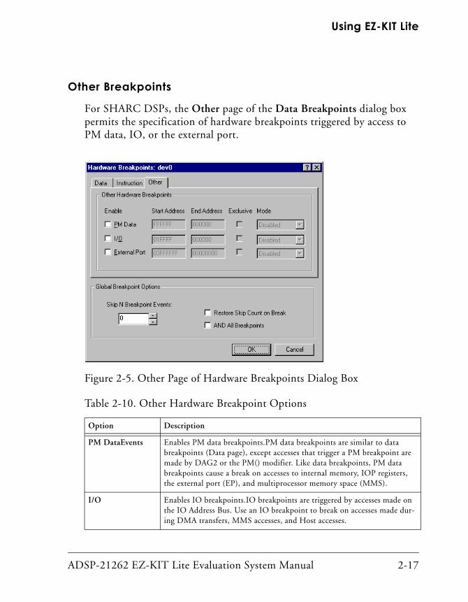
For SHARC DSPs, the Other page of the Data Breakpoints dialog box permits the specification of hardware breakpoints triggered by access to PM data, IO, or the external port.
Figure 2-5. Other Page of Hardware Breakpoints Dialog Box
Table 2-10. Other Hardware Breakpoint Options
Option Description
PM DataEvents Enables PM data breakpoints.PM data breakpoints are similar to data breakpoints (Data page), except accesses that trigger a PM breakpoint are made by DAG2 or the PM() modifier. Like data breakpoints, PM data breakpoints cause a break on accesses to internal memory, IOP registers, the external port (EP), and multiprocessor memory space (MMS).
I/O Enables IO breakpoints.IO breakpoints are triggered by accesses made on the IO Address Bus. Use an IO breakpoint to break on accesses made dur-ing DMA transfers, MMS accesses, and Host accesses.
ADSP-21262 EZ-KIT Lite Evaluation System Manual 2-17

Using EZ-KIT Lite VisualDSP++ Interface
Tips and Tricks Using Hardware Breakpoints
Be aware of the following tips and tricks when using hardware breakpoints on ADSP-21262 processors.
Latency
For SHARC processors, hardware breakpoints do not assert until two (2) instruction cycles after the actual break condition occurs
Restrictions
When using hardware breakpoints, do not place breaks at any address where a JUMP, CALL, or IDLE instruction would be illegal.
Do not place breaks in the last few instructions of a DO LOOP or in the delay slots of a delayed branch. For more information on these illegal loca-tions, refer to your DSP’s Hardware Reference.
Setting a Breakpoint on a Single Address
To set a breakpoint on a single address, set the Start Address equal to the End Address.
External Port Enables external port breakpoints.External port (EP) breakpoints are trig-gered by accesses made through the External Port. Use an EP breakpoint to break on accesses made to any external device that may be tied to the EP, such as external memory.
AND All Break-points
ANDs the interrupts to form the composite interrupt. Normally, the group interrupts are ORed to create a composite interrupt.
Table 2-10. Other Hardware Breakpoint Options (Cont’d)
Option Description
2-18 ADSP-21262 EZ-KIT Lite Evaluation System Manual
3 EZ-KIT LITE HARDWARE REFERENCE
This chapter describes the hardware design of the ADSP-21262 EZ-KIT
Lite board. The following topics are covered.• “System Architecture” on page 3-2Describes the configuration of the ADSP-21262 board and explains how the board components interface with the DSP.
• “DIP Switch Settings” on page 3-8Shows the location and describes the function of the DIP switches.
• “LEDs and Push Buttons” on page 3-12Shows the location and describes the function of the LEDs and push buttons.
• “Connectors” on page 3-15Shows the location and gives the part number for all of the connec-tors on the board. Also, the manufacturer and part number information is given for the mating parts.
ADSP-21262 EZ-KIT Lite Evaluation System Manual 3-1

System Architecture
System ArchitectureThis section describes the processor’s configuration on the EZ-KIT Lite board.
The EZ-KIT Lite has been designed to demonstrate the capabilities of the ADSP-21262 DSP. The DSP core is powered at 1.2V, and the IO is pow-ered at 3.3V. Two 0-ohm resistors give access to the DSP’s power planes and allow to measure the power consumption of the processor. The R79 resistor provides access to the IO voltage of the processor, and the R80 resistor provides access to the core voltage plane of the processor.
Figure 3-1. System Architecture Block Diagram
ADSP-21262DSP
SRAM
USB
Con
nect
or
EZ U
SB F
X
JTAGHeader
Power Regulation
PBs (4)
JTAG
Por
t
A5V
+7.5
VC
onne
ctor
ExpansionConnectors
Type A
1M x 8Flash
25 MHzOscillator
ParallelPort
3.3V
Stereo Out RCAJacks (4x2)
Stereo In RCAJacks (2x1)
DAI
1.2VAD1835CODEC
SPI
SPI FLASH
512k x 8SRAM
CS8416SPDIF RX Phono
FLAG0-3
GP LEDs(8)
2 2
HeadphoneJack
Reset PB
3-2 ADSP-21262 EZ-KIT Lite Evaluation System Manual

EZ-KIT Lite Hardware Reference
The CLKIN pin of the DSP connects to a 25 MHz oscillator. The core fre-quency of the DSP is derived by multiplying the frequency at the CLKIN pin by a value determined by the state of the DSP pins, CLKCFG1 and CLKCFG0. The value at these pins is determined by the state of the SW10 switch (see “Boot Mode and Clock Ratio Select Switch (SW10)” on page 3-11). By default, the EZ-KIT Lite gives a core frequency of 200 MHz.
The SW10 switch also configures the boot mode of the DSP. The EZ-KIT Lite is capable of Parallel Port boot and SPI Master Boot. By default, the EZ-KIT Lite boots from the parallel port. For information about config-uring the boot modes, see “Boot Mode and Clock Ratio Select Switch (SW10)” on page 3-11.
Parallel PortThe parallel port (PP) of the ADSP-21262 DSP consists of a 16-bit multi-plex address/data memory bus (AD15–0) and an address latch-enable pin (ALE). The interface does not have any memory select pins; these signals must be generated by decoding the address.
The PP connections to the EZ-KIT Lite are shown in Figure 3-2. The PP is connected to an 8-bit parallel Flash memory, an 8-bit SRAM memory, and eight general-purpose LEDs. The upper three address bits are con-nected to a 3-to-8 decoder, providing eight memory select pins. See “Using External Memory” on page 2-2 for more information about access-ing the Flash and SDRAM memories.
Because the PP is a multiplexed address/data memory bus, two 8-bit latches are used to latch the upper address bits. Additional latch is used to drive the LEDs. The latter allows the LED values to be written to as if they were at a memory location. For more information about using the LEDs, refer to the “Using LEDs and Push Buttons” on page 2-6.
All of the PP signals are available externally via the expansion interface connectors (J3–1). The pinout of the connectors can be found in “Sche-matics” on page B-1.
ADSP-21262 EZ-KIT Lite Evaluation System Manual 3-3

System Architecture
DAI InterfaceThe pins of the Digital Application Interface (DAI) connect to the signal routing unit (SRU). The SRU is a flexible routing system, providing a large system of signal flows within the DSP. In general, the SRU allows to route the DAI pins to different internal peripherals in various combinations.
Figure 3-2. Parallel Port Connections Block Diagram
DSP
AD15-0
ExpansionInterface
ALE
3738-bit
Latch
LE
D Q
3738-bit Latch
(2)
LE
D Q
512KBSRAM
D7-0
A8-18A0-7
CS
8 LEDs
Op ening the switchputs latch always inTranspa rent Mode
1MBFLASH
D7-0
A8-19A0-7
CSFLASH_C S
SRAM_CS
WR
SRAM_CS
FLASH_CSSRAM_CSLED_CS138
3->8DEC
0
21
34567
CBA
D0-7
A23A22A21
3-4 ADSP-21262 EZ-KIT Lite Evaluation System Manual

EZ-KIT Lite Hardware Reference
The DAI pins are connected to the AD1835A audio codec, the CS8414 SPDIF receiver, the audio oscillator output, and two push buttons. Figure 3-3 illustrates the EZ-KIT Lite’s connections to the DAI.
Refer to “Using Analog Audio” on page 2-3 and “Using Digital Audio” on page 2-5 for more information about setting up the DSP to communicate with these devices.
To use the DAI for a different purpose, disable any signal, which is driv-ing the DAI pins, with a switch. See “Codec Setup Switch (SW7)” on page 3-9 and “SPDIF Signal Enable Switch (SW8)” on page 3-10 for how to. In addition, the codec setup switch allows flexible routing of the 12.288 MHz audio oscillator’s output signal. By default, this signal is used as the master clock (MCLK) for the AD1835A codec.
Figure 3-3. DAI Connections Block Diagram
PB_3PB_4
4x2RCAPhonoJackOUT
Head-phoneJack
1X2RCAPhonoJack IN
PhonoJack
12.288MHz
SPDIF_IN
AD1835
DAC_LRCLKDAC_BCLKDAC_SDATA1DAC_SDATA2DAC_SDATA3DAC_SDATA4
ADC_LRCLKADC_BCLKADC_SDATA1
MCLK
ADC
DAC1DAC2DAC3DAC4
SPDIF RX
SPDIF_FSYNCSPDIF_SCLKSPDIF_SDATA
SPDIF_MCLK
IN
DSP
DAIP1DAIP2DAIP3DAIP4DAIP5DAIP6DAIP7DAIP8DAIP9
DAIP10DAIP11DAIP12
DAIP15DAIP16DAIP17DAIP18
DAIP20
DAIP14DAIP13
DAIP19
Audio_OSC
Audio_OSC
ADSP-21262 EZ-KIT Lite Evaluation System Manual 3-5
System Architecture
SPI InterfaceThe DSP’s serial peripheral interconnect (SPI) interface is connected to an SPI Flash memory, the CS8416 SPDIF receiver, and the AD1835A audio codec. The FLAG0 pin is used as a memory select for accessing the SPI Flash memory, and the FLAG3 pin is used for accessing the AD1835A’s configuration registers.
All of the SPI signals are available externally via the expansion interface connectors (J3–1), as well as the 0.1' spaced header P2. The pinout of these connectors can be found in “Schematics” on page B-1.
FLAG Pins
The DSP has four general-purpose IO FLAG pins. Table 3-1 describes the connection of each flag.
For information on how to disable the push buttons from driving the cor-responding DSP flag pin, see section “Push Button Enable Switch (SW9)” on page 3-10.
The FLAG signals are available externally via the expansion interface con-nectors (J3–1). The pinout of these connectors can be found in “Schematics” on page B-1.
Table 3-1. IO FLAG Pins
FLAG Pin EZ-KIT Lite Function
FLAG0 SPI Flash chip select
FLAG1 Push button (SW1) input
FLAG2 Push button (SW2) input
FLAG3 AD1835A SPI interface chip select
3-6 ADSP-21262 EZ-KIT Lite Evaluation System Manual

EZ-KIT Lite Hardware Reference
Expansion InterfaceThe expansion interface consists of the three 90-pin connectors. Table 3-2 shows the interfaces each connector provides. For the exact pinout of these connectors, refer to Appendix B, “Schematics” on page B-1. The mechan-ical dimensions of the connectors can be obtained from Technical or Customer Support.
Limits to the current and to the interface speed must be taken into consid-eration when using the expansion interface. The maximum current limit is dependent on the capabilities of the used regulator. Additional circuitry can also add extra loading to signals, decreasing their maximum effective speed.
Analog Devices does not support and is not responsible for the effects of additional circuitry.
JTAG Emulation PortThe JTAG emulation port allows an emulator to access the DSP’s internal and external memory through a 6-pin interface. The JTAG emulation port of the processor is also connected to the USB debugging interface. When an emulator connects to the board at P8, the USB debugging interface is disabled. This is not the standard connection of the JTAG interface.
Table 3-2. Expansion Interface Connectors
Connector Interfaces
J1 5V, AD15–0
J2 3.3V, FLAG3–0, DAI_P20–1, SPI
J3 5V, 3.3V, Reset, Parallel Port Control signals
ADSP-21262 EZ-KIT Lite Evaluation System Manual 3-7

DIP Switch Settings
For information about the standard connection of the interface, see EE-68 published on the Analog Devices website. For more information about the JTAG connector, see “JTAG Header (P5)” on page 3-19. To learn more about available emulators, contact Analog Devices (see “Product Information”).
DIP Switch SettingsFigure 3-4 shows the location and default settings of the EZ-KIT Lite DIP switches.
Figure 3-4. DIP Switch Locations and Default Settings
3-8 ADSP-21262 EZ-KIT Lite Evaluation System Manual

EZ-KIT Lite Hardware Reference
Electret Microphone Select Switch (SW6)To connect an electret microphone to the audio input, place all positions of the SW6 switch “ON”. The default position of this switch is all “OFF”. When all of the switches are in the “ON” position, a DC offset of 2.5V is added to the signal, and gain of the input amplifiers is changed from 1x to 10x.
Codec Setup Switch (SW7)The codec setup switch (SW7) can be used to change the routing of some of the signals going to the AD1835A codec and to setup the communication protocol of the codec.
Positions 1 and 2 determine the clock routing for the audio oscillator to the codec and to the DSP. Figure 3-5 illustrates how the switch positions 1 and 2 are connected on the board. In the default position, route the DAI_P17 pin to DAI_P6 (in software) to clock the AD1835A.
Position 3 of the SW7 switch determines if the AD1835A device is a master or is a slave. If the AD1835A is a master, the device’s serial interface gen-erates the frame sync and clock signals necessary to transfer data. When
Figure 3-5. Audio Clock Routing
AD1835 Codec
MCLK DAI_P6
ADSP-21262 DSP
DAI_P17
SW7.1
12.288MHzOSC
SW7.2
ADSP-21262 EZ-KIT Lite Evaluation System Manual 3-9

DIP Switch Settings
the device is a slave, the DSP must generate the frame sync and clock sig-nals. By default, position 3 is “ON”, and the AD1835A generates the control signals.
Position 4 of SW7 disconnects the AD1835A’s ADC_DATA pin from the DAI interface. This is useful when the DAI interface is to connect to another device.
SPDIF Signal Enable Switch (SW8)The SPDIF signal enable switch (SW8) disconnects always driving signal of the CS8416 SPDIF receiver serial interface.
Table 3-3 shows which DSP signal is no longer being driven when the corresponding switch position is placed in the “OFF” position.
Push Button Enable Switch (SW9)The push button enable switch (SW9) disconnects the push buttons from the corresponding DSP pins. This allows the signals to be used for another purpose. Table 3-4 shows the signal and SW9 connections. By default, all of the position of the SW9 switch are “ON”, allowing the push buttons to function as designed.
Table 3-3. SW8 Connections
Switch Position DSP Pin SPDIF RX Pin
1 DAI_P2 MCK
2 DAI_P1 SDATA
3 DAI_P4 FSYNC
4 DAI_P3 SCK
5 DAI_P15 SPI_CS
6 DAI_P16 GPO0
3-10 ADSP-21262 EZ-KIT Lite Evaluation System Manual

EZ-KIT Lite Hardware Reference
Position 6 of SW9 connects or disconnects the latch-enable pin of the LED to the logical “OR” of the ~WE and ~LED_CS signals. When position is “OFF”, the latch-enable pin of the LED latch ((U24) is always pulled “HIGH”, mak-ing the latch transparent. In this position, the value of the LEDs is directly connected to AD7–0. When position 6 is “ON”, the values of the LEDs are set by writing to a memory location. The lower 8 bits of the data written to the address 0x1400 0000 set the values of the LEDs. By default, position 6 is “ON”, allowing the LEDs to be written by writing to a memory address. For more information refer to “Using LEDs and Push Buttons” on page 2-6.
Boot Mode and Clock Ratio Select Switch (SW10)The SW10 switch sets the boot mode and clock multiplier ration. Table 3-5 shows how to set up the boot mode using positions 1 and 2. By default, the EZ-KIT Lite boots in SPI master mode and Parallel Port mode, and the DSP boots from Flash memory.
Table 3-4. Push Button Enable Switch (SW9) Connections
Switch Position Push Button Reference Designator DSP Pin
1 SW1 FLAG1
2 SW2 FLAG2
3 SW3 DAI19
4 SW4 DAI20
Table 3-5. Boot Mode Configuration
BOOTCFG1 Pin (Position 2) BOOTCFG0 Pin (Position 1) Boot Mode
OFF OFF SPI Slave Boot
OFF ON SPI Master Boot
ADSP-21262 EZ-KIT Lite Evaluation System Manual 3-11

LEDs and Push Buttons
Table 3-6 shows how to set up the clock multiply ratio using positions 3 and 4. By default, the DSP increases the clock multiply ratio by 8, setting the core clock to 300 MHz.
Loop-Back Test Switch (SW11)The loop-back test switch (SW11) is connected to GPO1 of the CS8416. The functionality of GPO1 is programmable via SPI.
LEDs and Push ButtonsThis section describes the functionality of the LEDs and push buttons. Figure 3-6 shows the locations of the LEDs and push buttons.
ON OFF Flash Boot1
ON ON Internal Boot Mode
1 Bold typeface denotes the default setting.
Table 3-6. Core Clock Rate Configuration
CLKCFG1 (Position 4) CLKCFG0 (Position 3) Core to CLKIN Ratio
OFF OFF 3:1
OFF ON 16:1
ON OFF 8:11
1 Bold typeface denotes the default ratio.
ON ON NA
Table 3-5. Boot Mode Configuration (Cont’d)
BOOTCFG1 Pin (Position 2) BOOTCFG0 Pin (Position 1) Boot Mode
3-12 ADSP-21262 EZ-KIT Lite Evaluation System Manual

EZ-KIT Lite Hardware Reference
General Purpose LEDs (LED8–1)Eight general-purpose LEDs are connected to the DSP through a latch on signals AD7–0. These LEDs can be accessed by writing to the FLAG registers or by writing to a memory address. Refer to “Using LEDs and Push But-tons” on page 2-6 for more information.
Figure 3-6. LED and Push Button Locations
ADSP-21262 EZ-KIT Lite Evaluation System Manual 3-13
LEDs and Push Buttons
Reset LEDs (LED9, LED12)When LED9 is lit (red), the master reset of all the major ICs is active. When LED12 is lit (red), the USB interface chip (U34) is being reset. The USB chip is reset only on power-up, or if USB communication has not been initialized.
Power LED (LED10)When LED10 is lit (green), it indicates that power is being properly sup-plied to the board.
SPDIF GPO1 LED (LED11)The SPDIF GPO1 LED (LED11) connects to GPO1 of the CS8416. The functionality of GPO1 is programmable via SPI.
USB Monitor LED (LED13)The USB monitor LED (LED13) indicates that USB communication has been initialized successfully and you may connect to the processor using a VisualDSP++ EZ-KIT Lite session. Once the USB cable is plugged into the board, it takes approximately 15 seconds for the USM monitor LED to light. If the LED does not light, try cycling power on the board and/or reinstalling the USB driver (see “Installing EZ-KIT Lite USB Driver” on page 1-7).
Push Buttons (SW4–1)Four push buttons (SW4–1) are provided for general-purpose user input. Two of the push buttons are connected to the DSP’s FLAG pins. The other two are connected to the DSP’s DAI. The push buttons are active “HIGH” and, when pressed, send a High (1) to the processor. Refer to “Using LEDs and Push Buttons” on page 2-6 for more information. The push
3-14 ADSP-21262 EZ-KIT Lite Evaluation System Manual

EZ-KIT Lite Hardware Reference
button enable switch (SW9) is capable of disconnecting the push buttons from the corresponding DSP pin (refer to “Push Button Enable Switch (SW9)” on page 3-10 on page 3-10 for more information). The DSP sig-nals and corresponding push buttons are summarized in Table 3-7.
Board Reset Push Button (SW5)The RESET push button (SW5) resets all of the ICs on the board. The only exception is the USB interface chip (U34). The chip is not being reset when the push button is pressed after the USB cable has been plugged in and communication correctly initialized with the PC. After USB commu-nication has been initialized, the only way to reset the USB is by powering down the board.
ConnectorsThis section describes the connector functionality and provides informa-tion about mating connectors. Figure 3-7 shows the connector locations.
Expansion Interface (J1, J2, J3)Three board-to-board connectors (J3–1) provide signals for most of the processor’s peripheral interfaces. The connectors are located at the bottom of the board. For more information about the expansion interface, see “Expansion Interface” on page 3-7. For the J3–1 connectors’ availability and pricing, contact Samtec.
Table 3-7. Push Button Connections
DSP Signal
Push Button Reference Designator
DSP Signal
Push Button Reference Designator
FLAG1 SW1 DAI_P19 SW3
FLAG2 SW2 DAI_P20 SW4
ADSP-21262 EZ-KIT Lite Evaluation System Manual 3-15

Connectors
Figure 3-7. Connector Locations
Part Description Manufacturer Part Number
90 Position 0.05" Spacing, SMT (J1, J2, J3)
Samtec SFC-145-T2-F-D-A
Mating Connector
90 Position 0.05” Spacing (Through Hole)
Samtec TFM-145-x1 Series
90 Position 0.05” Spacing (Surface Mount)
Samtec TFM-145-x2 Series
90 Position 0.05” Spacing (Low Cost)
Samtec TFC-145 Series
3-16 ADSP-21262 EZ-KIT Lite Evaluation System Manual

EZ-KIT Lite Hardware Reference
Audio In RCA Connector (J4)
Audio Out RCA Connector (J5)
Headphone Out Jack (J6)
Power Jack (J7)The power connector (J7) provides all of the power necessary to operate the EZ-KIT Lite board.
Part Description Manufacturer Part Number
Two channel right angle RCA jack SWITCHCRAFT PJRAS1X2S02
Mating Cable
Two channel RCA interconnect cable Monster Cable BI100-1M
Part Description Manufacturer Part Number
Six channel right angle RCA jack SWITCHCRAFT PJRAS2X2S01
Mating Cable
Two channel RCA interconnect cable Monster Cable BI100-1M
Part Description Manufacturer Part Number
3.5mm stereo jack (J6) Shogyo SJ-0359AM-5
Part Description Manufacturer Part Number
2.5 mm Power Jack (J7) SWITCHCRAFTDigi-Key
RAPC712SC1152-ND
Mating Power Supply (shipped with EZ-KIT Lite)
7.5V Power Supply GlobTek TR9CC2000LCP-Y
ADSP-21262 EZ-KIT Lite Evaluation System Manual 3-17

Connectors
The power connector supplies DC power to the EZ-KIT Lite board. Table 3-8 shows the power supply specifications.
SPDIF In Coax Connector (P1)
SPI Header (P2)The SPI connector (P2) provides access to all of the SPI signals in the from of a .1” spacing header. In addition, the FLAG1 signal can be used as a chip select. If you are using FLAG1 as a chip select, disable the push button asso-ciated with the flag. For more information, see “Push Button Enable Switch (SW9)” on page 3-10.
DAI Header (P3)The DAI connector (P3) provides access to all of the DAI signals in the from of a .1” spacing header. When using the header to access the DSP’s DAI pins, ensure that signals, which normally drive the DSP’s DAI pins,
Table 3-8. Power Supply Specifications
Terminal Connection
Center pin +7.5 VDC@2A
Outer Ring GND
Part Description Manufacturer Part Number
Coaxial (P1) SWITCHCRAFT PJRAN1X1U01
Part Description Manufacturer Part Number
6-pin IDC Header (P2) Sullins PTC04DAAN
3-18 ADSP-21262 EZ-KIT Lite Evaluation System Manual

EZ-KIT Lite Hardware Reference
are disabled. Refer to “Codec Setup Switch (SW7)” on page 3-9 for more information on how to disable signals already being driven from elsewhere on the EZ-KIT Lite.
USB Connector (P4)The USB connector (P4) allows to configure and program the DSP.
JTAG Header (P5)The JTAG header (P5) is the connecting point for a JTAG in-circuit emu-lator pod. When an emulator is connected to the JTAG header, the USB debug interface is disabled.
Pin 3 is missing to provide keying. Pin 3 in the mating connector should have a plug.
When using an emulator with the EZ-KIT Lite board, follow the connection instructions provided with the emulator.
Part Description Manufacturer Part Number
26-pin IDC Header (P3) Berg 54102-T08-13
Part Description Manufacturer Part Number
Type B USB receptacle (P4) Mill-MaxDigi-Key
897-30-004-90-000 ED90003-ND
Part Description Manufacturer Part Number
14-pin IDC Header (P5) Berg 54102-T08-07
ADSP-21262 EZ-KIT Lite Evaluation System Manual 3-19

Connectors
3-20 ADSP-21262 EZ-KIT Lite Evaluation System Manual

A BILL OF MATERIALS
r
Ref
eren
ce
Qua
ntit
y
Des
crip
tion
Ref
eren
ce D
esig
n
Man
ufac
ture
Par
t N
umbe
r
1 1 AM29LV08IB-120EC TSOP40 1M-X-8-FLASH-3V
U19 AMD AM29LV081-120E
2 2 74LVC14A SOIC14 HEX-INVER-SCHMITT-TRIGGER
U28,U33 TI 74LVC14AD
3 1 CS8416 SOIC28 96KHZ-DIGI-TAL-AUDIO-RECVR
U3 CIRRUS LOGIC
CS8416
4 1 CY7C64603-128 PQFP128 USB-TX/RX MICROCON-TROLLER
U34 CYPRESS CY7C64603-128N
5 1 MMBT4401 SOT-23 NPN TRANSISTOR 200MA
Q1 FAIRCHILD MMBT4401
6 1 74LVC00AD SOIC14 U13 PHILIPS 74LVC00AD
7 1 CY7C1019BV33-15VC SOJ32 128K X 8 SRAM
U29 CYPRESS CY7C1019BV33-1
8 1 AD8532AR SOIC8 DUAL AMP 250MA
U10 ANALOG DEVICES
AD8532AR
ADSP-21262 EZ-KIT Lite Evaluation System Manual A-1

9 2 SN74AHC1G02 SOT23-5 SINGLE-2 INPUT-NOR
U26,U36 TI SN74AHC1G02DB
10 1 SN74LV164A SOIC14 8-BIT-PARALLEL-SERIAL
U35 TI SN74LV164AD
11 1 CY7C4201V-15AC TQFP32 64-BYTE-FIFO
U32 CYPRESS CY7C4201V-15AC
12 1 25MHZ 1/2 OSC01 OSC
U16 DIGI-KEY SG-8002DC-PCC-
13 1 12.0MHZ THR OSC006 CRYSTAL
Y1 DIG01 300-6027-ND
14 2 SN74AHC1G00 SOT23-5 SINGLE-2-INPUT-NAND
U20,U27 TI SN74AHC1G00DB
15 1 12.288MHZ SMT OSC003 TS201/21262
U17 DIG01 SG-8002CA-PCC-
16 1 74LVC138AD SOIC16 3-TO-8-DEMUX
U25 PHILIPS 74LVC138AD
17 3 74LVC373APW TSSOP20 8-BIT-D-LATCH
U18,U21,U24
PHILIPS 74LVC373APW
18 1 21262 24LC00 “U23” SEE 1000127
U23 MICRO-CHIP
24LC00-SN
19 1 IS61LV5128AL TSOP44 512KX8-SRAM
U15 ISSI IS61LV5128AL-10
20 1 AT25F512N SOIC8 SPI-FLASH-512KB
U12 ATMEL AT25F512N-10SI-2
21 1 LTC1877 SOIC8 600MA ADJ SWITCHING REG
VR5 LINEAR TECH
LTC1877EMS8
Ref
eren
ce
Qua
ntit
y
Des
crip
tion
Ref
eren
ce D
esig
n
Man
ufac
ture
r
Par
t N
umbe
r
A-2 ADSP-21262 EZ-KIT Lite Evaluation System Manual
Bill Of Materials
22 2 1000pF 50V 5% 1206 CERM
C37–38 AVX 12065A102JAT2A
23 8 2200pF 50V 5% 1206 NPO
C67–74 AVX 12065A222JAT05
24 1 ADM708SAR SOIC8 VOLTAGE-SUPERVISOR
U22 ANALOG DEVICES
ADM708SAR
25 1 ADP3339AKC-33 SOT-223 3.3V 1.5A REGULATOR
VR2 ANALOG DEVICES
ADP3339AKC-3.3
26 2 ADP3336ARM MSOP8 ADJ 500MA REGULATOR
VR1,VR4 ANALOG DEVICES
ADP3336ARM-RE
27 8 AD8606AR SOIC8 OPAMP
U2,U4–9,U11
ANALOG DEVICES
AD8606AR
28 1 ADSP-21262SKBC-200 BGA136SHARC-EX-DSP
U1 ANALOG DEVICES
ADSP-21262SKBC
29 1 AD1835AAS MQFP52 2IN-8OUT-96KHZ-CODEC
U14 ANALOG DEVICES
AD1835AAS
30 5 RUBBER FEET BLACK MH1–5 MOUSER 517-SJ-5018BK
31 1 PWR 2.5MM_JACK CON005 RA
J7 SWITCH-CRAFT
SC1152-ND12
32 1 USB 4PIN CON009 USB
P4 MILL-MAX 897-30-004-90-00
33 1 RCA 4X2 CON011 RA
J5 SWITCH-CRAFT
PJRAS4X2U01
34 1 RCA 1X1 CON012 BLK
P1 SWITCH-CRAFT
PJRAN1X1U01
Ref
eren
ce
Qua
ntit
y
Des
crip
tion
Ref
eren
ce D
esig
n
Man
ufac
ture
r
Par
t N
umbe
r
ADSP-21262 EZ-KIT Lite Evaluation System Manual A-3
35 5 SPST-MOMENTARY SWT013 6MM
SW1–5 PANASONIC EVQ-PAD04M
36 3 0.05 45X2 CON019 SMT SOCKET
J1–3 SAMTEC SFC-145-T2-F-D-A
37 1 DIP8 SWT016 SW11 C&K CKN1365-ND
38 1 DIP6 SWT017 SW8 DIG01 CKN1364-ND
39 4 DIP4 SWT018 4PIN-SMT-SWT
SW6–7, SW9–10 DIG01 CKN1363-ND
40 1 RCA RCA_1X2 CON031 RA
J4 SWITCH-CRAFT
PJRAS1X2S02
41 2 0.00 1/8W 5% 1206 R82,R91 YAGEO 0.0ECT-ND
42 10 AMBER-SMT LED001 GULL-WING
LED1–8,LED11,LED13
PANASONIC LN1461C-TR
43 8 330pF 50V 5% 805 NPO
C104,C106,C108,C110,C11,C114,
AVX 08055A331JAT
44 18 0.01uF 100V 10% 805 CERM
C66, C75, C79, C85, C122, C127, C153, C155, C157–164, C166, C182
AVX 08051C103KAT2A
45 8 0.22uF 25V 10% 805 CERM
C77,C87,C99–102,C111,C131
AVX 08053C224FAT
46 27 0.1uF 50V 10% 805 CERM
C47,C57,C59,C120–121, C132–133
AVX 08055C104KAT
Ref
eren
ce
Qua
ntit
y
Des
crip
tion
Ref
eren
ce D
esig
n
Man
ufac
ture
r
Par
t N
umbe
r
A-4 ADSP-21262 EZ-KIT Lite Evaluation System Manual

Bill Of Materials
47 4 0.001uF 50V 5% 805 NPO
C82–83,C88,C98 AVX 08055A102JAT2A
48 44 10K 100MW 5% 805 R4, R17, R63–64, R66, R70–71, R74–78, R90, R92, R96–102, R107–108,
AVX CR21-103J-T
49 4 33 100MW 5% 805 R68,R81,R109,R135 AVX CR21-330JTR
50 3 4.7K 100MW 5% 805 R72,R95,R176 AVX CR21-4701F-T
51 1 680 100MW 5% 805 R137 AVX CR21-6800F-T
52 1 1M 100MW 5% 805 R168 AVX CR21-1004F-T
53 1 475 100MW 5% 805 R125 AVX CR21-471J-T
54 1 1.5K 100MW 5% 805 R105 AVX CR21-1501F-T
55 2 2.00K 1/8W 1% 1206 R3,R5 DALE CR32-2001F-T
56 10 49.9K 1/8W 1% 1206 R114–115,R117–124
AVX CR32-4992F-T
57 2 2.21K 1/8W 1% 1206 R93–94 AVX CR32-2211F-T
58 12 100pF 100V 5% 1206 NPO
C2–12,C64 AVX 12061A101JAT2A
59 2 10uF 16V 10% B TANT
CT13–14 AVX TAJB106K016R
60 4 100 100MW 5% 805 R185–188 AVX CR21-101J-T
61 2 301 1/4W 1% 1206 R1–2 BOURNS CR1206-FX-3010
Ref
eren
ce
Qua
ntit
y
Des
crip
tion
Ref
eren
ce D
esig
n
Man
ufac
ture
r
Par
t N
umbe
r
ADSP-21262 EZ-KIT Lite Evaluation System Manual A-5

62 9 220pf 50V 10% 1206 NPO
C183 AVX 12061A221JAT2A
63 2 2A S2A_RECT DO-214AA SILICON RECTIFIER
D1–2 GENER-ALSEMI
S2A
64 7 600 100MHZ 500MA 1206 0.70 BEAD
FER1–2,FER4–8 DIGI-KEY 240-1019-1-ND
65 4 237 1/8W 1% 1206 R13–14,R18,R20 AVX CR32-2370F-T
66 2 750K 1/8W 1% 1206 R11,R116 DALE/VISHAY
CRCW12067503F
67 4 5.76K 1/8W 1% 1206 R6,R10,R19,R22 PHYCOMP 9C12063A5761FK
68 10 11.0K 1/8W 1% 1206 R47,R49–50,R52–53,R55–56,R58, R113,R136
DALE CRCW12061102F
69 1 68NF 50V 10% 805 C65 MURRATA GRM40X7R683K0
70 7 1UF 16V 10% 805 X7R
C1,C39,C44,C48,C56,C58,C61
MURATA GRM40X7R105K0
71 1 75 1/8W 5% 1206 R112 PHILIPS 9C12063A75R0JL
72 3 30PF 100V 5% 1206 C55 AVX 12061A300JAT2A
73 1 10 100MW 5% 805 R150 DALE CRCW0805-10R0
74 1 249K 1/10W 1% 805 R86 DALE CRCW0805-2493
75 1 124K 1/10W 1% 805 R83 DALE CRCW0805-1243F
76 12 680PF 50V 1% 805 NPO
C76,C80–81,C89,C103,C105,C107
AVX 08055A681FAT2A
Ref
eren
ce
Qua
ntit
y
Des
crip
tion
Ref
eren
ce D
esig
n
Man
ufac
ture
r
Par
t N
umbe
r
A-6 ADSP-21262 EZ-KIT Lite Evaluation System Manual
Bill Of Materials
77 3 10UF 25V +80-20% 1210 Y5V
C46,C49,C60 MURATA GRM235Y.5V106Z
78 8 2.74K 1/8W 1% 1206 R140–147 DALE CRCW12062741F
79 20 5.49K 1/8W 1% 1206 R7,R15–16,R21,R25,R28,R31,R34,
PANASONIC ERJ-8ENF5491V
80 8 1.65K 1/8W 1% 1206 R23,R26,R29,R32,R35,R38,R41,
PANASONIC ERJ-8ENF1651V
81 10 10UF 16V 20% CAP002 ELEC
CT1–9,CT12 DIG01 PCE3062TR-ND
82 2 68UF 25V 20% CAP003 ELEC
CT10–11 PANASONIC EEV-FC1E680P
83 1 10UH 47 +/-20 IND001 L1 DIG01 445-1202-2-ND
84 7 0.00 100MW 5% 805 R192 VISHAY CRCW0805 0.0 R
85 1 190 100MHZ 5A FER002 FER3 MURATA DLW5BSN191SQ2
86 8 3.32K 100MW 1% 805 R24,R27,R30,R33,R36,R39,R42,
DIG01 P3.32KCCTR-ND
87 4 1.2K 1/10W 5% 805 R155–158 DALE CRCW08051201F
88 9 10UF 6.3V 10% 805 C184–185 AVX 080560106KAT2A
89 3 6.04K 100MW 1% 805 R65,R148–149 DIGI-KEY 311-6.04KCCT-ND
90 7 0.1UF 10V 10% 402 C41,C128–129, C136
AVX 0402ZD104KAT2A
91 5 0.01UF 16V 10% 402 C134,C138,C147,C149,C151
AVX 0402YC103KAT2A
Ref
eren
ce
Qua
ntit
y
Des
crip
tion
Ref
eren
ce D
esig
n
Man
ufac
ture
r
Par
t N
umbe
r
ADSP-21262 EZ-KIT Lite Evaluation System Manual A-7

92 8 1000PF 50V 5% 402 CERM
C130,C135,C137,C139,C143,C146,
AVX 04025C102JAT2A
93 2 64.9K 1/10W 1% 805 R67,R87 VISHAY INTERTEC
CRCW08056492F
94 2 210K 1/4W 1% 805 R69,R88 VISHAY INTERTEC
CRCW08052103F
95 1 1A SK12 DO-214AA SCHOTTKY
D3 MCC SK12
96 21 10PF 50V 5% 805 NPO
C21–25,C27–36,C42–43,C123–126
AVX 08055A100JAT2A
97 1 1K 1/8W 5% 1206 R106 AVX CR32-102J-T
98 1 100K 1/8W 5% 1206 R73 DALE CR1206-1003FRT
99 2 22 1/8W 5% 1206 R103–104 DALE CRCW1206220JR
100 12 270 1/8W 5% 1206 R138–139,R153–154, R177–184
AVX CR32-271J-T
101 2 RED-SMT LED001 GULL-WING
LED9,LED12 PANASONIC LN1261C
102 1 GREEN-SMT LED001 GULL-WING
LED10 PANASONIC LN1361C
103 8 604 1/8W 1% 1206 R127–134 DALE CRCW12066040F
104 4 1uF 25V 20% A TANT -55+125
CT15–18 PANASONIC ECS-T1EY105R
105 2 ADG774A QSOP16 QUICKSWITCH-257
U30–31 ANALOG DEV.
ADG774ABRQ
Ref
eren
ce
Qua
ntit
y
Des
crip
tion
Ref
eren
ce D
esig
n
Man
ufac
ture
r
Par
t N
umbe
r
A-8 ADSP-21262 EZ-KIT Lite Evaluation System Manual

Bill Of Materials
106 1 IDC 3X2 IDC3X2 P2 BERG 54102-T08-03
107 1 IDC 7X2 IDC7X2 HEADER
P5 BERG 54102-T08-07
108 1 IDC 13X2 IDC13X2 P3 BERG 54102-T08-13
109 1 2.5A RESETABLE FUS001 F1 RAYCHEM CORP.
SMD250-2
110 1 3.5MM STEREO_JACK CON001
J6 SHOGYO SJ-0359AM-5
Ref
eren
ce
Qua
ntit
y
Des
crip
tion
Ref
eren
ce D
esig
n
Man
ufac
ture
r
Par
t N
umbe
r
ADSP-21262 EZ-KIT Lite Evaluation System Manual A-9

A-10 ADSP-21262 EZ-KIT Lite Evaluation System Manual
A0174-2002 1.4
4
3
2
1
A B C D
20 Cotton Road
Nashua, NH 03063
A B C D
4
3
2
1
PH: 1-800-ANALOGD
C
Title
Size Board No.
Date Sheet of
Rev
DEVICESANALOG
DNP = Do Not Populate
ADSP-21262 EZ-KIT Lite Schematic
12111-7-2003_19:25
ADSP-21262 EZ-KIT LITE - TITLE

3.3V
3.3V
3.3V
A0174-2002 1.4
4
3
2
1
A B C D
20 Cotton Road
Nashua, NH 03063
A B C D
4
3
2
1
PH: 1-800-ANALOGD
C
Title
Size Board No.
Date Sheet of
Rev
DEVICESANALOG
DNP = Do Not Populate
3.3V
3.3V
3.3V
OE OUT
AD0
AD4
AD5
AD6
AD7
AD8
AD9
AD10
AD11
AD12
AD13
AD14
AD15
RD
WR
ALE
EMU
TMS
TCK
TRST
TDI
TDO
CLKOUT
CLKIN
XTAL
RESET
DAIP1/SD0A
DAIP2/SD0B
DAIP3/SCLK0
DAIP4/SFS0
DAIP5/SD1A
DAIP6/SD1B
DAIP7/SCLK1
DAIP8/SFS1
DAIP9/SD2A
DAIP10/SD2B
DAIP11/SD3A
DAIP12/SD3B
DAIP13/SCLK23
DAIP14/SFS23
DAIP15/SD4A
DAIP16/SD4B
DAIP17/SD5A
DAIP18/SD5B
DAIP19/SCLK45
DAIP20/SFS45
MISO
MOSI
SPICLK
SPIDS
FLAG0
FLAG1
FLAG2
FLAG3
BOOTCFG0
BOOTCFG1
CLKCFG0
CLKCFG1
AD3
AD2
AD1VDDEXT1
VDDEXT2
VDDEXT3
VDDEXT6
VDDINT1
VDDINT2
VDDINT3
VDDINT4
VDDINT5
VDDINT6
VDDINT7
VDDINT8
VDDINT9
VDDINT10
VDDINT11
VDDINT12
VDDINT13
AVDD
AVSS
GND1
GND2
GND3
GND4
GND5
GND6
GND7
GND11
GND12
GND13
GND14
GND15
GND16
GND17
GND18
GND19
GND20
GND21
GND22
GND23
GND24
GND25
GND26
GND27
GND28
GND29
GND30
GND31
GND32
GND33
GND34
GND35
GND36
GND37
GND38
GND39
GND40
GND41
GND42
GND43
GND44
GND45
GND46
GND47
GND48
GND49
GND50
GND51
GND52
GND53
GND54
VDDEXT4
VDDEXT5
GND8
GND9
GND10
ON1
23
4
OSC
ON
OFF
ON
OFF
OFFOFF
ON
SPI MASTER BOOTPARALLEL PORT BOOTRESERVED
BOOTMODE
CLOCK RATIOCORE:CLKIN
3:1
RESERVED
ADSP-21262ADSP-21262
1 2
3 4
SPI SLAVE BOOT
DSP OSC
DEFAULT
BOOTCFG1BOOTCFG0
CLKCFG0 CLKCFG1
OFFONOFF ON
ON OFF8:1
16:1DEFAULTONOFF
Place as close as possible to pin B07 and B06 of DSP
These capacitors were placed on the board due to a DSP anomaly. Please refer to the DSP anomaly sheet for more information.
SW10: BOOT/CLOCK RATIO SELECT(Default: 1=ON, 2=OFF, 3=ON, 4=OFF)
ON
DAIP15_SPDIF_SPI_CS
1-23-2004_12:23 2 12
2
3
1
4 5
6
7
8SW10
SWT018DIP4
B7
B6
A13
D2
D4
D5
D6
D9
D10
D11
D13
E2
E4
A14
E5
E6
E9
E10
E11
E13
F4
F5
F6
F9
B2
F10
F11
J4
J5
J6
J9
J10
J11
K4
K5
B12
K6
K9
K10
K11
K13
L4
L5
L6
L9
L10
B13
L11
L13
M3
M12
N13
B14
C3
C12
C13
B3
B8
G13
H2
N5
N9
A12
N4
N7
N11
N12
B11
C14
D1
D14
E1
G2
J13
K2
U1
BGA136ADSP-21262SKBC-200
M1
L2
P5
P4
P3
P2
P1
N1
L1
K1
J2
J1
H1
G1
N6
P6
N2
C2
C1
A1
B1
B4
A6
N14
P14
M13
M14
L14
K14
J14
H14
H13
G14
P7
N8
F14
P8
N10
P9
P10
P11
P12
P13
F2
F1
F13
E14
A10
A9
B9A4
A5
A7
A3
A2
A8
N3
B10
A11B5
M2
U1
BGA136ADSP-21262SKBC-200
DAIP14_DAC_LRCLKDAIP15_SPDIF_SPI_CS
DAIP16_SPDIF_GPO0DAIP17_AUDIO_OSC
TCK
TMS
1000PF402
C143 C154
4021000PF 10UF
805
C260.1UF402
C142C128
4020.1UF0.01UF
402
C134C151
4020.01UF1000PF
402
C130C135
4021000PF
C145
80510UF
C136
4020.1UF0.1UF
402
C129C149
4020.01UF0.01UF
402
C138C150
4021000PF1000PF
402
C137C139
4021000PF1000PF
402
C146
4020.1UFC140
EMU
DAIP6_AD1835_MCLK
10PF805
C42
1 5
U16
OSC00125MHZ25MHZ
DAIP6_AD1835_MCLK
DSP_CLKIN
DAIP1_SPDIF_DATADAIP2_SPDIF_MCLK
DAIP3_SPDIF_SCKDAIP4_SPDIF_FSYNC
DAIP5_ADC_DATA DAIP7_ADC_BCLKDAIP8_ADC_LRCLK
DAIP9_DAC_D4DAIP10_DAC_D3
DAIP11_DAC_D2DAIP12_DAC_D1
DAIP13_DAC_BCLKDAIP18_SPDIF_IN
DAIP19_SW3DAIP20_SW4
SPICLK
SPIDS
SPICLK
MOSI
R790.00805
TDO
TDI
TRST
AD[0:15]AD1
AD0
AD2
AD3
AD4
AD5
AD6
AD7
AD8
AD9
AD10
AD11
AD12
AD13
AD14
AD15
R7810K805
C144
4020.1UF
C1470.01UF402
D3
DO-214AA
SK121A
R16010K805805
10KR159
R6833805
C45
8050.1UF
DNP
4.7K805
R72
10K805
R7110K805
R75R77
80510K
R15210K805
3.3V_DSP
DSP_CLKIN
8051.2KR155
R16210K805
R1561.2K805
R1581.2K805
80510KR161
ADSP-21262 EZ-KIT LITE - DSP
R15010805
3.3V_DSP
1.2V_DSP
8051.2KR157
RESET
DSP_CLKOUT
ALE
WE
RD
DAIP1_SPDIF_DATA
DAIP2_SPDIF_MCLK
DAIP3_SPDIF_SCK
DAIP4_SPDIF_FSYNC
DAIP5_ADC_DATA
DAIP7_ADC_BCLK
DAIP8_ADC_LRCLK
DAIP9_DAC_D4
DAIP10_DAC_D3
DAIP11_DAC_D2
DAIP12_DAC_D1
DAIP13_DAC_BCLK
DAIP14_DAC_LRCLK
DAIP16_SPDIF_GPO0
DAIP17_AUDIO_OSC
DAIP18_SPDIF_IN
DAIP19_SW3
DAIP20_SW4
MISO
FLAG0_SPI_FLASH_CS
FLAG1_SW1
FLAG2_SW2
FLAG3_AD1835_SPI_CS
3.3V_DSP
1.2V_DSP
C34
80510PF 10PF
805
C36 C31
80510PF 10PF
805
C33 C30
80510PF10PF
805
C32C43
80510PF10PF
805
C35 C24
80510PF 10PF
805
C126 C124
80510PF 10PF
805
C2710PF805
C23 C125
80510PF 10PF
805
C28 C29
80510PF
C25
80510PF 10PF
805
C123 C22
80510PF 10PF
805
C21
1.2V1.2V_DSP
8050.00R80

3.3V
3.3V3.3V3.3V
A0174-2002 1.4
4
3
2
1
A B C D
20 Cotton Road
Nashua, NH 03063
A B C D
4
3
2
1
PH: 1-800-ANALOGD
C
Title
Size Board No.
Date Sheet of
Rev
DEVICESANALOG
DNP = Do Not Populate
3.3V
3.3V
3.3V
3.3V
3.3V3.3V
3.3V
2D
3D
4D
5D
6D
7D
8D
GND
LE VCC
OE
1D 1Q
2Q
3Q
4Q
5Q
6Q
7Q
8Q
A
B
C
G1
G2A
G2B
Y0
Y1
Y2
Y3
Y4
Y5
Y6
Y7
GND
VCC
2D
3D
4D
5D
6D
7D
8D
GND
LE VCC
OE
1D 1Q
2Q
3Q
4Q
5Q
6Q
7Q
8Q
SCK
SI
CS
VCC
SO
GND
HOLD
WP
A0
A1
A2
A3
A4
A5
A6
A7
A8
A9
A10
A11
A12
A13
A14
A15
A16
A17
A18
A19
NC/A20
CE
OE
WE
D0
D1
D2
D3
D4
D5
D6
D7
NC1
NC2
RY/BY
RESET
VCC1
VCC2
VSS1
VSS2
A0
A1
A2
A3
A4
A5
A6
A7
A8
A9
A10
A11
A12
A13
A14
A15
A16
A17
A18
NC/A19
D0
D1
D2
D3
D4
D5
D6
D7
NC1
NC2
NC3
NC4
NC5
NC6
NC7
NC8
NC9
VDD1
VDD2
GND1
GND2
CE
OE
WE
3.3V-
0110
0 0000
A22 A21
-
01
110 0
Y0Y1Y2Y3Y4
1
FLASHSRAMLEDsEXPANSION INTERFACE CS 1EXPANSION INTERFACE CS 2NONE
ENDSTARTVALID DSP ADDRESS
A23ADDRESSBANK END
BANK DEVICE
-XXX
74LVC138 AT25F512 74LVC373 IS61LV512874LVC373 AM29LV081
4Mb (512K x 8-bit) 8Mb (1M x 8-bit)SRAM Flash
512KbSPI Flash
1A0 0000180 0000160 0000140 0000120 0000100 0000 10F FFFF
127 FFFF140 0000
11F FFFF13F FFFF15F FFFF17F FFFF19F FFFF1FF FFFF
1231-23-2004_13:10
R6610K805 805
10KR64
C1560.1UF805
0.01UF805
C1530.1UF805
C141C158
8050.01UF0.01UF
805
C1600.01UF805
C1270.01UF805
C163
3
4
5
6
7
16
17
18
19
20
26
27
28
29
30
38
39
40
41
25
9
10
13
14
31
32
35
36
1
2
21
22
23
24
42
43
44
11
33
12
34
8
37
15
U15
TSOP44IS61LV5128AL
21
20
19
18
17
16
15
14
8
7
36
6
5
4
3
2
1
40
13
37
38
22
24
9
25
26
27
28
32
33
34
35
11
29
12
10
31
30
39
23
U19
TSOP40AM29LV081B-120EC
7
6
5
1
3
8
2
4
U12
SOIC8AT25F512N
3
4
7
8
13
14
17
18
11
1
2
5
6
9
12
15
16
19
20
10
U21
TSSOP2074LVC373APW
1
2
3
6
4
5
15
14
13
12
11
10
9
7
8
16
U25
SOIC1674LVC138AD
10
20
19
16
15
12
9
6
5
2
1
11
18
17
14
13
8
7
4
3
U18
TSSOP2074LVC373APW
RESET
EXP_CS1
EXP_CS2
MISO
MOSI
SPICLK
80510KR163
LED_CS
WE RD
FLASH_CS
SRAM_CS
FLASH_CS
ALE
ALE
A20
A19
A8
A9
A13
A16
A17
A18
A15
A14
A12
A11
A10
A[8:20]
AD0
AD1
AD2
AD3
AD4
AD5
AD6
AD7
AD[0:7]
A[8:19]
A18
A19
A17
A8
A9
A13
A16
A15
A14
A12
A11
A10
A[8:23]A9
A10
A11
A12
A13
A14
A15
A8
A23
A22
A21
A20
A19
A18
A17
A16
AD7
AD6
AD5
AD4
AD3
AD2
AD1
AD0AD[0:15]
AD8
AD9
AD10
AD11
AD12
AD13
AD14
AD15
ADSP-21262 EZ-KIT LITE - MEMORY
AD8
AD9
AD11
AD12
AD13
AD14
AD15
AD10
AD[8:15] AD[0:7]
AD7
AD6
AD5
AD4
AD3
AD2
AD1
AD0AD8
AD9
AD11
AD12
AD13
AD14
AD15
AD10
AD[8:15]
SRAM_CS
WE
RD
RESET
A[21:23]A21
A22
A23
0.01UF805
C157
FLAG0_SPI_FLASH_CS

A5V
AGND
A5V3.3V3.3V
A5V
AGND
A5V
AGND
3.3V
AGND
5V
3.3V
5V
AGND
A0174-2002 1.4
4
3
2
1
A B C D
20 Cotton Road
Nashua, NH 03063
A B C D
4
3
2
1
PH: 1-800-ANALOGD
C
Title
Size Board No.
Date Sheet of
Rev
DEVICESANALOG
DNP = Do Not Populate
ABCLK
ALRCLK
ASDATA
DBCLK
DLRCLK
DSDATA1
DSDATA2
DSDATA3
DSDATA4
MCLK
CIN
COUT
CCLK
CLATCH
~M/S
PD/RST
ODVDD
DVDD1
DVDD2
DGND1
DGND2
ADCLN
ADCLP
ADCRN
ADCRP
OUTRP1
OUTRN1
OUTLP1
OUTLN1
OUTRP2
OUTRN2
OUTLP2
OUTLN2
OUTRP3
OUTRN3
OUTLP3
OUTLN3
OUTRP4
OUTRN4
OUTLP4
OUTLN4
FILTD
FILTR
AVDD1
AVDD2
AVDD3
AGND1
AGND2
AGND3
AGND4
AGND5
AGND6
OE OUT
3.3V
3.3V
81
24
56
7
ON
3
ON1
23
4
OSC
DAC1
DAC4
DAC3
DAC2
ADCA
DC
AD8606
AD1835 AUDIOCODEC
DA
C4
RIGHT (RED)
LEFT (WHITE)
DA
C1
DA
C2
DA
C3
DA
C4
Loopback Test Switch
AD1835 AD1835AD1835
IN (J4) OUT (J5) OUT (J6)
(Default= All OFF)For Test Purposes Only
AUDIO OSC
1-2Connects or disconnects the audio oscillatordepending on how the system is setup.See users manual for more information.
OFF = AD1835 is SLAVEON = AD1835 is MASTER
Disconnects ADC_DATA signal fromdriving the corrisponding DAI signal.Useful if using this DAI pin for another purpose.
3
4
SW7: CODEC SETUP SWITCH(Default: 1=OFF, 2=ON, 3=ON, 4=ON)
2
3
1
4 5
6
7
8SW7
SWT018DIP4
8
1
2
7
3
6
5
4
16
15
14
13
12
11
10
9
SW11
SWT016DIP8
12411-7-2003_18:38
FLAG3_AD1835_SPI_CS
80510KR76
R7010K805
2
3
1
SOIC8AD8606AR
U11
DAIP17_AUDIO_OSC
RESET
1 3
OSC00312.288MHZ
U17
0.22UF805
C1310.1UF805
C133
8050.1UFC132
6
7
5
U11
AD8606ARSOIC8
R1510.00805
1206600FER8
8050.1UFC152
8050.1UFC148C155
8050.01UF0.1UF
402
C41
B10UFCT14
45
46
49
38
37
41
42
43
44
47
3
50
51
2
36
4
48
1
39
40
52
20
21
22
23
9
8
7
6
15
14
13
12
28
27
26
25
34
33
32
31
17
18
11
19
29
5
10
16
24
30
35
U14
MQFP52AD1835AAS
MASTER_SLAVE
ADSP-21262 EZ-KIT LITE - ANALOG AUDIO
5V_B
R149
8056.04K
6.04K805
R148
R65
8056.04K
AUDIO_VREF_ADC
0.1UF805
C12110UFB
CT13
8050.1UFC120
DAIP5_ADC_DATA
33805
R81
AUDIO_VREF_DAC
80510KR74
ADC_DATA
DAIP14_DAC_LRCLK
DAIP12_DAC_D1
DAIP7_ADC_BCLK
DAIP8_ADC_LRCLK
DAIP13_DAC_BCLK
DAIP11_DAC_D2
DAIP10_DAC_D3
DAIP9_DAC_D4
DAIP6_AD1835_MCLK
SPICLK
OUTLN1
OUTLP1
OUTRN1
OUTRP1
ADCRP
ADCRN
ADCLP
ADCLN
MISO
MOSI
OUTLN4
OUTLP4
OUTRN4
OUTRP4
OUTLN3
OUTLP3
OUTRN3
OUTRP3
OUTLN2
OUTLP2
OUTRN2
OUTRP2
AIN_RIGHT
AOUT4_RIGHT
AOUT2_RIGHT
AOUT2_LEFT
AOUT1_RIGHT
AOUT1_LEFT
AOUT3_LEFT
AOUT3_RIGHT
AOUT4_LEFT
AIN_LEFT
MASTER_SLAVE
DAIP6_AD1835_MCLK
ADC_DATA

A5V
AGND
A5V
AGND
AGND AGND
AGND
A0174-2002 1.4
4
3
2
1
A B C D
20 Cotton Road
Nashua, NH 03063
A B C D
4
3
2
1
PH: 1-800-ANALOGD
C
Title
Size Board No.
Date Sheet of
Rev
DEVICESANALOG
DNP = Do Not Populate
AGND
AD8606AD8606
DAC1 RIGHT DAC2 RIGHT
DAC2 LEFTDAC1 LEFT
120611.0KR55
R5311.0K12061206
11.0KR56
R5811.0K1206
1258-19-2003_22:57
C99
8050.22UF0.22UF
805
C100
R140
12062.74K
AUDIO_VREF_DAC
R54
12065.49K5.49K
1206
R57
5
6
J5
CON0114X2
3
2
4X2CON011
J5
1
3
2
AD8606ARSOIC8
U8
7
5
6
AD8606ARSOIC8
U8
2
3
1
U9
SOIC8AD8606AR
6
5
7
U9
SOIC8AD8606AR
C20DNP
805 805DNP
C18
805DNP
C19 C17DNP
805
8053.32KR36
R453.32K805
220PF1206
C90
CAP00210UFCT9
2200PF1206
C68
AOUT2_RIGHT
AOUT2_LEFT
AOUT1_RIGHT
AOUT1_LEFT
OUTRP2
OUTRN1
OUTRP1
OUTLP2
OUTLN2OUTLN1
OUTLP1
100PF1206
C115.49K1206
R46
330PF805
C112
680PF805
C103
ADSP-21262 EZ-KIT LITE - AUDIO OUT 1
49.9K1206
R118
1206604R127
1.65K1206
R44 R38
12061.65K
R1296041206 CT7
10UFCAP002
R120
120649.9K
C92
1206220PF
C70
12062200PF
C105
805680PF
C114
805330PF
R40
12065.49K C9
1206100PF
100PF1206
C85.49K1206
R37
330PF805
C106
680PF805
C115
2200PF1206
C69220PF1206
C93
49.9K1206
R119
CAP00210UFCT61206
604R130
1.65K1206
R355.49K1206
R61R62
12065.49K
R41
12061.65K
R1286041206 CT8
10UFCAP002
R117
120649.9K
C91
1206220PF
C67
12062200PF
C113
805680PF
C104
805330PF
R43
12065.49K C10
1206100PF
8053.32KR42
R393.32K805
1
3
J5
CON0114X2
4
6
J5
CON0114X2
AUDIO_VREF_DAC
AUDIO_VREF_DAC
AUDIO_VREF_DAC
2.74K1206
R141
R142
12062.74K
2.74K1206
R143
OUTRN2
A5V
AGND
A5V
AGND
AGND AGND
AGNDAGND
A0174-2002 1.4
4
3
2
1
A B C D
20 Cotton Road
Nashua, NH 03063
A B C D
4
3
2
1
PH: 1-800-ANALOGD
C
Title
Size Board No.
Date Sheet of
Rev
DEVICESANALOG
DNP = Do Not Populate
AD8606AD8606
DAC3 LEFT
DAC3 RIGHT DAC4 RIGHT
DAC4 LEFT
R4911.0K1206
120611.0KR47R50
11.0K1206
120611.0KR52
8-19-2003_22:57 6 12
C101
8050.22UF0.22UF
805
C102
2
3
1
U6
SOIC8AD8606AR
AOUT4_RIGHT_HP
AOUT4_LEFT_HPAOUT4_LEFT
CT310UFCAP002
12
11
4X2CON011
J5
9
8
4X2CON011
J5
7
5
6
AD8606ARSOIC8
U6
2
3
1
U7
SOIC8AD8606AR
7
5
6 U7
SOIC8AD8606AR
49.9K1206
R123
AOUT4_RIGHT
805DNP
C14C16DNP
805
805DNP
C15 C13DNP
805
OUTRN4
OUTRP4
OUTLN4
OUTLP4
OUTRN3
OUTRP3
OUTLN3
OUTLP3
ADSP-21262 EZ-KIT LITE - AUDIO OUT 2
100PF1206
C75.49K1206
R34
330PF805
C116
680PF805
C107
2200PF1206
C72220PF1206
C94
49.9K1206
R122
CAP00210UFCT51206
604R131
1.65K1206
R325.49K1206
R51 R48
12065.49K
R26
12061.65K
R1336041206
R124
120649.9K
C96
1206220PF
C74
12062200PF
C109
805680PF
C118
805330PF
R28
12065.49K C5
1206100PF
100PF1206
C45.49K1206
R25
330PF805
C110
680PF805
C119
2200PF1206
C73220PF1206
C97
CAP00210UFCT21206
604R134
1.65K1206
R235.49K1206
R59R60
12065.49K
R29
12061.65K
R1326041206 CT4
10UFCAP002
R121
120649.9K
C95
1206220PF
C71
12062200PF
C117
805680PF
C108
805330PF
R31
12065.49K C6
1206100PF
AOUT3_LEFT
AOUT3_RIGHT
R333.32K805
8053.32KR30
R273.32K805
8053.32KR24
9
7
4X2CON011
J5
10
12
J5
CON0114X2
AUDIO_VREF_DAC
AUDIO_VREF_DAC AUDIO_VREF_DAC
AUDIO_VREF_DAC
2.74K1206
R144 R146
12062.74K
2.74K1206
R147R145
12062.74K

AGND
A5V
AGND
A5V
A5V
AGND
AGND
AGND
AGND
AGND
AGND
AGND
A5V
AGND
AGND
A0174-2002 1.4
4
3
2
1
A B C D
20 Cotton Road
Nashua, NH 03063
A B C D
4
3
2
1
PH: 1-800-ANALOGD
C
Title
Size Board No.
Date Sheet of
Rev
DEVICESANALOG
DNP = Do Not Populate
AGND
AGND
ON1
23
4
AGND
AD8606
AD8606
AD8606AD8532
HEADPHONE OUT
DAC4
ELECTRET MICROPHONE ENABLE SWITCH(Default = All OFF)
WHEN USING AN ELECTRET MICROPHONEPLACE ALL SWITCHES IN ON POSITION
ADC RIGHT
ADC LEFT
3
1
2
SOIC8AD8606AR
U4
C84
80510UF
7
5
6 U10
AD8532ARSOIC8
1
3
2 U5
AD8606ARSOIC8
0.22UF805
C87 C77
8050.22UF 0.22UF
805
C111
6
5
7
SOIC8AD8606AR
U2
6
7
5
U4
AD8606ARSOIC8
1
3
2 U10
AD8532ARSOIC8
7-3-2003_17:09 7 12
C78120PF1206
DNP
12065.76KR6
DNP
1206120PFC86
3
1
J4
CON031RCA_1X2
3
2
J4
CON031RCA_1X2
1206301R2
R13011206
120611.0KR113
805680PFC76
12065.49KR7
237R14
1206
C81680PF805
R155.49K1206
12065.49KR21
805680PFC89
VREF_MIC_R
VREF_MIC_R
VREF_MIC_L
VREF_MIC_L
AIN_LEFT
C80680PF805
R165.49K1206
R13611.0K1206
AUDIO_VREF_ADC
AUDIO_VREF_ADC
AOUT4_LEFT_HP
AOUT4_RIGHT_HP
CT10
CAP00368UF
AIN_RIGHT2
3
1
4 5
6
7
8SW6
SWT018DIP4
2.00K1206
R3
R5
12062.00K
AUDIO_VREF_ADC
12065.76KR10
2
3
1
SOIC8AD8606AR
U2
1206
R13237
8050.001UFC82
CAP00210UFCT1
1206600FER6
1206100PFC64
AIN_RIGHT
7
5
6 U5
AD8606ARSOIC8
237R20
1206
1206
R18237
C12100PF1206
1206100PFC3
R126
8050.00
0.00805
R12ADCRP
CT11
CAP00368UFAUDIO_VREF_ADC
1
4
3
2
5
J6
CON001
ADSP-21262 EZ-KIT LITE - HEADPHONE OUT
R11449.9K1206
R11549.9K1206
CT1210UFCAP002
R195.76K1206
R225.76K1206
C2100PF1206
FER76001206
R11750K1206
C880.001UF805
C980.001UF805
8050.001UFC83
1206750KR116
ADCRN
ADCLN
AUDIO_VREF_ADC
ADCLP
AUDIO_VREF_ADC
AIN_LEFT

SHGND
3.3V
A0174-2002 1.4
4
3
2
1
A B C D
20 Cotton Road
Nashua, NH 03063
A B C D
4
3
2
1
PH: 1-800-ANALOGD
C
Title
Size Board No.
Date Sheet of
Rev
DEVICESANALOG
DNP = Do Not Populate
12
34
56
ON
3.3V
3.3V
3.3V
RCA
AGND
CCLK_SCL
CDIN_AD1
CDOUT_SDA
CS_ADO
DGND
FILT GPO0
GPO1
GPO2_AD0
OLRCK
OMCK
OSCLK
RMCK
RST
RXN
RXP0
RXP1
RXP2
RXP3
RXP4
RXP5
RXP6
RXP7
SDOUT
VA
VD
VL
SPDIF GPO1
SPDIFCOAXINPUT
CS8416
S/PDIF RX
(Default: ALL = ON)
1-6Used to disconnect signals of the SPDIF intefacefrom the corrisponding DAI signals.Useful if using DAI signals for another purpose.
SW8: SPDIF SIGNAL DISABLE
R137
805270
1281-28-2004_11:01
C650.022UF805
5
4
3
2
1
10
11
12
13
6
7
8
21
23
22
27
28
26
24
25
16
15
17
14
20
19
18
9
U3
SOIC28CS8416-CS
SPDIF_SCK
2
1
1X1CON012
P1
805
C122
DNP
0.1UF R4
8050.00
120675R112
C187
8050.1UF
C660.01UF805
R1253.01K1206
A3.3V
8050.00
DNPR8
8050.01UFC188
C850.001UF805
SPDIF_SPI_CS
SPDIF_FSYNC
SPDIF_SDATAR13533805
R9810K805
R1747K805
R6310K805
C1
8050.1UF
A3.3V
DAIP3_SPDIF_SCK
DAIP15_SPDIF_SPI_CS
SPDIF_GPO0
SPDIF_SCK
MISO
MOSI
TP8
RESET
1
10
11
12
2
3
4
5
6 7
8
9
SW8
SWT017DIP6
11 10
U33
74LVC14ASOIC14
0.001UF805
C79
SPDIF_FSYNCDAIP4_SPDIF_FSYNC
SPDIF_MCKDAIP2_SPDIF_MCLK
DAIP1_SPDIF_DATA SPDIF_SDATA
R90.00805
DAIP18_SPDIF_IN
ADSP-21262 EZ-KIT LITE - S/PDIF RX
C75
121010UF
1206600FER1
SPDIF_GPO0
SPICLK
SPDIF_SPI_CS
DAIP16_SPDIF_GPO0
0.1UF805
C186
SPDIF_MCK
LED11
LED001AMBER-SMT
3.3V
3.3V
3.3V
3.3V
3.3V
3.3V
3.3V
3.3V
A0174-2002 1.4
4
3
2
1
A B C D
20 Cotton Road
Nashua, NH 03063
A B C D
4
3
2
1
PH: 1-800-ANALOGD
C
Title
Size Board No.
Date Sheet of
Rev
DEVICESANALOG
DNP = Do Not Populate
3.3V
3.3V
3.3V
3.3V
2D
3D
4D
5D
6D
7D
8D
GND
LE VCC
OE
1D 1Q
2Q
3Q
4Q
5Q
6Q
7Q
8Q
PFI
RESETMR
PFO
RESET
12
34
56
ON
3.3V3.3V
SN74AHC1G02
6
5 Not Used
OFF = LEDs function as flagsON = LEDs are accessed at a memory address
AD0AD7 AD1AD6 AD2AD5 AD3AD4
74LVC373 ADM708
RESET
RESETPOWER
FLAG1
FLAG2
DAIP19
DAIP20
74LVC14A
LEDs can be accessed as a memeory address,or directly as flags depending on the DSP settings.
Lite User Manual for more information.
1-4 driving the corrisponding DSP signal.Used to stop the pushbuttons from
Useful if using these DSP signals for another purpose.
SW9: PUSH BUTTON ENABLE SWITCH
See SW9 Settings and the EZ-KIT
(Default = All ON, except position 5)
C162
8050.01UF
1
10
11
12
2
3
4
5
6 7
8
9
SW9
SWT017DIP6
1-23-2004_13:09 9 12
LED_CS_SW
C182
8050.01UF
80510KR172
0.01UF805
C161C164
8050.01UF
LED10GREEN-SMTLED001
RESET
LED001RED-SMTLED9
RESET_TO_USB4
81
5
7
SOIC8ADM708SAR
U22
LED1
LED001AMBER-SMTAMBER-SMT
LED001
LED2LED3
LED001AMBER-SMTAMBER-SMT
LED001
LED4LED5
LED001AMBER-SMTAMBER-SMT
LED001
LED6LED7
LED001AMBER-SMTAMBER-SMT
LED001
LED8
3
4
7
8
13
14
17
18
11
1
2
5
6
9
12
15
16
19
20
10
U24
TSSOP2074LVC373APW
SPST-MOMENTARYSWT013SW4
SWT013SPST-MOMENTARY
SW5
13 12
U33
74LVC14ASOIC14
SWT013SPST-MOMENTARY
SW1
SPST-MOMENTARYSWT013SW2
SWT013SPST-MOMENTARY
SW3
21
74LVC14ASOIC14
U33
A1UFCT18
80510KR174
805100R188
R16410K805
80510KR92
SOFT_RESET
80510KR96
1206270R138
R182
1206270
R184
1206270270
1206
R1832701206
R181R180
1206270270
1206
R179R178
1206270270
1206
R177
ADSP-21262 EZ-KIT LITE - USER IO/RESET
100805
R185
9 8
SOIC1474LVC14A
U33
805100R186
65
SOIC1474LVC14A
U33
10K805
R171
3 4
74LVC14ASOIC14
U33100805
R187
A1UFCT16
1UFA
CT15
10K805
R173
1UFA
CT17
AD[0:15]AD0
AD1
AD2
AD3
AD4
AD5
AD6
AD7
FLAG1_SW1
DAIP20_SW4
DAIP19_SW3
FLAG2_SW2
R1392701206
WE
LED_CS1
24
SOT23-5
U26
SN74AHC1G02

A0174-2002 1.4
4
3
2
1
A B C D
20 Cotton Road
Nashua, NH 03063
A B C D
4
3
2
1
PH: 1-800-ANALOGD
C
Title
Size Board No.
Date Sheet of
Rev
DEVICESANALOG
DNP = Do Not Populate
3.3V 5V3.3V5V
3.3V
All USB interface circuitry is considered proprietary and has
HEADER
EXPANSION INTERFACE (TYPE A)
HEADERSPI
DAIHEADER
JTAG
been omitted from this schematic.
When designing your JTAG interface please refer to theEngineer to Engineer Note EE-68 which can be found athttp://www.analog.com
See page 9NOTE: Must disable SW1 when using this pin as SPI select.
1-23-2004_12:23 10 12
FLAG2_SW2
FLAG2_SW2
FLAG0_SPI_FLASH_CS
FLAG1_SW1
FLAG3_AD1835_SPI_CS
FLAG1_SW1
87
85
83
81
77
75
73
69
67
65
63
61
59
57
1
10
1112
1314
1516
1718
19
2
20
2122
2324
2526
2728
29
3
30
3132
3334
3536
3738
39
4
40
4142
4344
4546
4748
5
50
6
78
9
49
55
51
53
52
54
56
58
60
62
66
70
68
72
74
76
78
80
82
84
86
88
90 89
64
71
79
45X2CON019
J1
87
85
83
81
77
75
73
69
67
65
63
61
59
57
1
10
1112
1314
1516
1718
19
2
20
2122
2324
2526
2728
29
3
30
3132
3334
3536
3738
39
4
40
4142
4344
4546
4748
5
50
6
78
9
49
55
51
53
52
54
56
58
60
62
66
70
68
72
74
76
78
80
82
84
86
88
90 89
64
71
79
45X2CON019
J3
87
85
83
81
77
75
73
69
67
65
63
61
59
57
1
10
1112
1314
1516
1718
19
2
20
2122
2324
2526
2728
29
3
30
3132
3334
3536
3738
39
4
40
4142
4344
4546
4748
5
50
6
78
9
49
55
51
53
52
54
56
58
60
62
66
70
68
72
74
76
78
80
82
84
86
88
90 89
64
71
79
45X2CON019
J2
EMULATOR_TDO
1
3
5
7
9
11
13
2
4
6
8
10
12
14
P5
IDC7X27X2
7
2
4
8
10
6
3
9
11
13
15
17
19
21
23
25
12
14
16
24
26
22
20
18
1
5
P3
IDC13X213X2
2
4
5 6
3
1P2
IDC3X23X2
8054.7KR176
1.2V_DSP
EMULATOR_SELECT
3.3V_DSP
1.2V
EXP_CS2
ALE
DAIP20_SW4
DAIP18_SPDIF_IN
DAIP16_SPDIF_GPO0
DAIP14_DAC_LRCLK
DAIP12_DAC_D1
DAIP10_DAC_D3
DAIP8_ADC_LRCLK
DAIP6_AD1835_MCLK
DAIP4_SPDIF_FSYNC
DAIP19_SW3
DAIP17_AUDIO_OSC
DAIP15_SPDIF_SPI_CS
DAIP13_DAC_BCLK
DAIP11_DAC_D2
DAIP9_DAC_D4
DAIP7_ADC_BCLK
DAIP5_ADC_DATA
DAIP3_SPDIF_SCK
DAIP1_SPDIF_DATA
DSP_CLKOUT
WE
RD
SPICLK
SPIDS
MOSI
MISO
ADSP-21262 EZ-KIT LITE - CONNECTORS
SPIDS
SPICLK
EMULATOR_TCK
EMULATOR_TMS
EMULATOR_TDI
EMULATOR_TRST
EMULATOR_EMU
MISO
MOSI
DAIP2_SPDIF_MCLK
RESET
RESET
DAIP2_SPDIF_MCLKDAIP1_SPDIF_DATA
DAIP3_SPDIF_SCK
DAIP5_ADC_DATA
DAIP7_ADC_BCLK
DAIP9_DAC_D4
DAIP4_SPDIF_FSYNC
DAIP6_AD1835_MCLK
DAIP8_ADC_LRCLK
DAIP10_DAC_D3
DAIP11_DAC_D2
DAIP15_SPDIF_SPI_CS
DAIP13_DAC_BCLK
DAIP17_AUDIO_OSC
DAIP19_SW3 DAIP20_SW4
DAIP18_SPDIF_IN
DAIP16_SPDIF_GPO0
DAIP14_DAC_LRCLK
DAIP12_DAC_D1
AD13
AD11
AD9
AD7
AD5
AD3
AD1
AD15
AD12
AD10
AD8
AD6
AD4
AD2
AD0
AD14
AD[0:15]
EXP_CS1

5V
SHGND
SHGND
3.3V
A0174-2002 1.4
4
3
2
1
A B C D
20 Cotton Road
Nashua, NH 03063
A B C D
4
3
2
1
PH: 1-800-ANALOGD
C
Title
Size Board No.
Date Sheet of
Rev
DEVICESANALOG
DNP = Do Not Populate
3.3V
SHGND
GND
INPUT OUTPUT1
OUTPUT2
CHOKE_COIL
OUT1
OUT2
OUT3
IN1
IN2
FBSD GND
OUT1
OUT2
OUT3
IN1
IN2
FBSD GND
COMP
DRV
FB
GND1 GND2
IN1
IN2
SW
ITH
VIN SYNC_MODE
VFB
SWRUN
GND PLL_LPF
POPULATIONOPTION
30pF
220pF
DNP
249K
124K
DNP
0
DNP
LTC1877
DNP
DNP
470pF
10pF
20K
470pF
221K
53.6K
POP
DNP
DNP
DNP
ADP3088
316K
C55
C183
R84
C53
R86
R83
D4
R192
R191
VR5
VR3
R89
POWER IN
DNP
OPTIONPOPULATIONADP3088
LTC1877
(DEFAULT)REFERENCEDESIGNATOR
TP5
C60
121010UF
5V_B
1-23-2004_11:59 11 12
2
6 7
3
51
4 8
VR5
MSOP8LTC1877
DNP805316KR89
C185
80510UF
249KR86
805
R83124K805
R8420.0K1206DNP
C53470PF1206DNP
30PFC55
1206
1206220PFC183
805
R191DNP
10UF805
C184C51
80510UF10UF
805
C50
C49
121010UF
8051UFC48
D41ADO-214AA
DNP
L1
IND00110UH
1
2
3
4
7
8
6
5
VR3
MSOP8ADP3088
DNP
0.00R192
805
DNPR85
805
C54
805DNP
1.2V
C590.1UF805
C57
8050.1UF
C44
8051UF
8051UFC61
4
6 5
8
7
3
2
1
ADP3336ARMMSOP8
VR11
2
3
7
8
56
4
VR4
MSOP8ADP3336ARM805
0.1UFC47
10UF1210
C46
C561UF805 805
10UFC52 C40
10UF805805
1UFC39
C581UF805
R910.001206
4
1
3
2
FER3
TP7TP4TP6TP2
1206600FER5
6001206
FER2
1
3
4
2
VR2
SOT-223ADP3339AKC-33
UNREG_IN
12061000PFC37
1206100KR73
DO-214AA2AD2
FUS0012.5AF1
1
3
2
CON0052.5MM_JACK
7.5V_POWER
J7
UNREG_IN
UNREG_IN
TP3
ADSP-21262 EZ-KIT LITE - POWER
12061000PFC38
DO-214AA2AD1
MH5 MH4 MH3MH2MH1
80564.9KR87
R88210K805
R820.001206
UNREG_IN
805210KR69
R6764.9K805
TP1
UNREG_IN
I INDEX
Symbols SPI port, 2-4
~LED_CS signal, 3-11~WE signal, 3-11Aabort, hang operations, 2-11acknowledge, hang operation, 2-11AD15-0 pins, 3-3AD1835A audio codec, xiii, 2-3, 2-5,
3-6, 3-9ADC_DATA pin, 3-10configuration registers, 2-4master mode, 2-4, 3-9slave mode, 2-4, 2-5, 3-10
AD7-0 pins, 2-6, 3-11, 3-13Add New Hardware Wizard, Windows
98, 1-8ADSP-21262 processors
boot mode, 3-11CLKCFG1, CLKCFG0 pins, 3-3core frequency, 3-3core voltage, 3-2external memory map, 2-2flash memory, 2-2internal memory restrictions, 2-2IO voltage, 3-2parallel port, 2-2, 2-7
SRAM memory, 2-2analog
audio interface, xii, 2-3to-digital converters (ADCs), 2-3
audioapplications, xiiiin RCA connector (J4), 3-17oscillator, 3-9out RCA connector (J5), 3-17
Bbackground telemetry channel (BTC),
2-8bill of materials, A-1boot
code, 2-2load, 2-8mode, 3-3, 3-11
BOOTCFG pins, 3-11breakpoints, 2-12
Cchip select, 2-3, 3-18clear, hang operations, 2-11CLKIN pin, 3-3clock
ADSP-21262 EZ-KIT Lite Evaluation System Manual I-1

INDEX
multiplier ratio, 3-11routing, 3-9signals, 3-9
codec setup switch (SW7), 3-9common attributes, hardware
breakpoints, 2-13connecting, EZ-KIT Lite board, 1-5connectors, 1-5, 3-15
J1 (expansion interface), 3-7J2 (expansion interface), 3-7J3 (expansion interface), 3-7J4 (audio in RCA), 2-4, 3-17J5 (audio out RCA), 2-4, 3-17J6 (headphone out), 2-4, 3-17J7 (power), 3-17P1 (SPDIF In Coax), 3-18P2 (SPI), 3-18P3 (DAI), 3-18P4 (USB), 1-6, 3-19P5 (JTAG header), 3-19P8 (JTAG), 3-7
contents, EZ-KIT Lite package, 1-1conventions, manual, xxicore hang conditions, 2-11CS8416, xiii, 2-5, 3-6, 3-10, 3-12,
3-14customer support, xvi
DDAI
header (P3), xiii, 3-18pins, 2-6, 3-11, 3-15port, 2-3, 2-5
data
hardware breakpoints, 2-14IO rate, 2-3transfer, 3-9
Device Manager window, 1-16digital
audio interface (DAI), xiii, 3-14to-analog converters (DACs), 2-3
DIP switches, 2-6, 3-8also see SW
DSP signalsDAI pins, 3-11, 3-15FLAG pins, 3-11, 3-15
Eelectret microphone, 2-4, 3-9electrostatic discharge, 1-2enable attribute, 2-13end address, attribute, 2-13example programs, 2-7exclusive, attribute, 2-13expansion interface, xiii, 3-15
see also connectorsexternal memory, 2-3, 3-7EZ-KIT Lite board
architecture, 3-2boot modes, 3-11features, xii
Ffeatures, EZ-KIT Lite board, xiiFLAG pins, 2-7, 3-6, 3-14
FLAG0, 2-3FLAG1, 3-18FLAG10, 2-7
I-2 ADSP-21262 EZ-KIT Lite Evaluation System Manual

INDEX
FLAG11, 2-7FLAG12, 2-7FLAG13, 2-7FLAG14, 2-7FLAG15, 2-7FLAG3, 2-4FLAG8, 2-7FLAG9, 2-7
FLAG registers, 2-6, 3-13flash memory, xiii, 2-3, 3-3, 3-6, 3-11
see also external memoryFound New Hardware Wizard
Windows 2000, 1-14frame sync signals, 2-4, 2-5, 3-9
Ggeneral-purpose IO
FLAG pins, 3-6LEDs, 2-6, 3-3, 3-13push buttons
see push buttonsglobal options, hardware breakpoints,
2-14graphical user interface (GUI), 2-8
Hhard reset, 2-8hardware breakpoint, 2-12, 2-17
dialog box, 2-12restrictions, 2-18
headphone out jack (J6), 3-17Help, online, xixhung conditions, 2-11
II2S mode, 2-3ignore, hang operations, 2-11installation, summary, 1-3installing
EZ-KIT Lite USB driver, 1-7VisualDSP++ and EZ-KIT Lite
license, 1-4VisualDSP++ and EZ-KIT Lite
software, 1-4instruction hardware breakpoints, 2-15interfaces
see graphical user interface (GUI)internal memory, 3-7interrupts, 2-6IO
FLAG pins, 3-6voltage, 3-2
JJ3-1 connectors, 3-15JTAG
connector (P5), 3-19emulation port, 3-7emulator, 3-19ICE, xiii
jumper settings, 1-5
Llatch-enable pin (ALE), 2-6, 3-3, 3-11latency, 2-18LEDs, xiii, 1-5, 2-6, 3-11, 3-12
LED10, 1-6, 3-14LED11, 1-15, 1-16, 2-5, 3-14
ADSP-21262 EZ-KIT Lite Evaluation System Manual I-3

INDEX
LED12, 1-6, 3-14LED13, 3-14LED8-1 (general purpose), 3-13LED9, 1-6, 3-14
license restrictions, 2-2loop-back test switch (SW11), 3-12
Mmaster input clock (MCLK), 2-4memory
bus (AD15-0), 3-3restrictions, 2-2
mode, attribute, 2-13
Ooscillator, 2-4, 3-3
Ppackage contents, 1-1parallel
flash memory, 2-2port, 2-2, 2-6, 3-3, 3-11port boot, 3-3
PCconfiguration, 1-3
peripheral ports, xivpins, 3-9power
connector (J7), 3-17LED (LED10), 3-14specifications, 3-18supply, 3-18
PPFLGS bit, 2-7
processor external memory, see ADSP-21262 processors
program memory, xii, 2-2push buttons, xiii, 2-6, 3-12
see also SWSW1 (general input), 3-14, 3-15SW2 (general input), 3-14, 3-15SW3 (general input), 3-14, 3-15SW4 (general input), 3-14, 3-15SW5 (reset), 3-15SW9 (enable), 3-10
RR79 resistor, 3-2R80 resistor, 3-2registering, this product, 1-2, 1-4reset
board, 2-8hang operation, 2-11processor, 3-14push button (SW5), 3-15
retry, hang operation, 2-11
SSerial Peripheral Interconnect (SPI),
xii, 3-6serial port clock, 2-4setting
breakpoints, 2-18EZ-KIT Lite hardware, 1-5target options, 2-9
spacing headers, 3-18SPDIF
GPO1 LED (LED11), 3-14
I-4 ADSP-21262 EZ-KIT Lite Evaluation System Manual

INDEX
receiver, 2-4, 3-10setup, 3-10
SPIflash memory, 2-2header (P2), xiii, 3-18master boot, 3-3master mode, 3-11
SRAM memory, xiii, 2-2, 3-3start address, attribute, 2-13starting VisualDSP++, 1-16SW10 switch, 3-3SW11 switch, 3-12SW6 switch, 3-9SW7 switch, 3-9SW8 switch, 3-10SW9 switch, 3-15system
architecture, EZ-KIT Lite board, 3-2requirements, PC, 1-3
Ttarget options
miscellaneous, 2-10on emulator exit, 2-9while target is halted, 2-9
target options dialog box, 2-9
time-division multiplexed mode (TDM), 2-3
UU24, LED latch, 3-11USB
cable, 1-2, 3-14, 3-15connector (P4), 3-19debug interface, 3-19driver installation, Windows 2000,
1-12driver installation, Windows 98, 1-8driver installation, Windows XP, 1-13interface, 3-7interface chip (U34), 3-14, 3-15monitor LED (LED13), 3-14
Vverifying USB driver installation, 1-15VisualDSP++
documentation, xixinstallation, 1-4license, 1-4online Help, xixrequirements, 1-3starting, 1-16
ADSP-21262 EZ-KIT Lite Evaluation System Manual I-5

INDEX
I-6 ADSP-21262 EZ-KIT Lite Evaluation System Manual