Embed Size (px)
Citation preview

Adsorbing H2S onto a single graphene sheet: A possible gas sensorA. H. Reshak and S. Auluck Citation: Journal of Applied Physics 116, 103702 (2014); doi: 10.1063/1.4894840 View online: http://dx.doi.org/10.1063/1.4894840 View Table of Contents: http://scitation.aip.org/content/aip/journal/jap/116/10?ver=pdfcov Published by the AIP Publishing Articles you may be interested in Graphene/mica based ammonia gas sensors Appl. Phys. Lett. 105, 254102 (2014); 10.1063/1.4905039 Edge and substrate-induced bandgap in zigzag graphene nanoribbons on the hexagonal nitride boron 8-ZGNR/h-BN(0001) AIP Advances 3, 092105 (2013); 10.1063/1.4821110 Trilayer graphene nanoribbon carrier statistics in degenerate and non degenerate limits AIP Conf. Proc. 1499, 272 (2012); 10.1063/1.4769000 Density functional theory study of BN-doped graphene superlattice: Role of geometrical shape and size J. Appl. Phys. 108, 073711 (2010); 10.1063/1.3487959 Electronic structure and optical properties of Sb-doped SnO 2 J. Appl. Phys. 106, 083701 (2009); 10.1063/1.3245333
[This article is copyrighted as indicated in the article. Reuse of AIP content is subject to the terms at: http://scitation.aip.org/termsconditions. Downloaded to ] IP:
14.139.60.97 On: Wed, 22 Apr 2015 10:57:03

Adsorbing H2S onto a single graphene sheet: A possible gas sensor
A. H. Reshak1,2,a) and S. Auluck3
1New Technologies-Research Centre, University of West Bohemia, Univerzitni 8, 306 14 Pilsen,Czech Republic2Center of Excellence Geopolymer and Green Technology, School of Material Engineering,University Malaysia Perlis, 01007 Kangar, Perlis, Malaysia3Council of Scientific and Industrial Research-National Physical Laboratory, Dr. K S Krishnan Marg,New Delhi 110012, India
(Received 15 July 2014; accepted 26 August 2014; published online 8 September 2014)
The electronic structure of pristine graphene sheet and the resulting structure of adsorbing a single
molecule of H2S on pristine graphene in three different sites (bridge, top, and hollow) are studied
using the full potential linearized augmented plane wave method. Our calculations show that the
adsorption of H2S molecule on the bridge site opens up a small direct energy gap of about 0.1 eV at
symmetry point M, while adsorption of H2S on top site opens a gap of 0.3 eV around the symmetry
point K. We find that adsorbed H2S onto the hollow site of pristine graphene sheet causes to push
the conduction band minimum and the valence band maximum towards Fermi level resulting in a
metallic behavior. Comparing the angular momentum decomposition of the atoms projected
electronic density of states of pristine graphene sheet with that of H2S–graphene for three different
cases, we find a significant influence of the location of the H2S molecule on the electronic
properties especially the strong hybridization between H2S molecule and graphene sheet. VC 2014AIP Publishing LLC. [http://dx.doi.org/10.1063/1.4894840]
I. INTRODUCTION
A honeycomb two dimensional lattice of monolayer car-
bon atoms, a new material called graphene, was discovered
recently.1,2 Graphene consists of a single atomic layer of sp2
hybridized carbon atoms that result in a hexagonal lattice.
Around each carbon atom, three strong r bonds are estab-
lished with the other three surrounding carbon atoms.3
Research on graphene has opened a new era in nanotechnol-
ogy. The outstanding mechanical,4 electrical,5 and physical
properties6 of graphene warrants its use in a variety of areas
such as hydrogen technology,7 electronics,5 sensing,8 and
drug delivery,9,10 among many others. The zero band gap of
the graphene at point K renders the construction of graphene
based field effect transistors very difficult. Therefore, several
groups have proposed different methods to open a band gap
in graphene.11–23 Denis et al.13 found that when graphene is
doped with sulfur a band gap is opened depending on the sul-
fur content. It is found that graphene, which is more accessi-
ble to doping and chemical modification at the same time, is
more susceptible to structural defects and impurities.
Graphene is considered the most promising adsorbent for the
adsorption of gases.24–26 Hegde et al.27 have used the first-
principles density functional theory (DFT) to determine the
chemical activity of carbon site of pristine graphene, Stone-
Wales defect site, and BN-sites of BN-doped graphene
towards adsorption of toxic gas H2S. Recently, DFT calcula-
tions were used to investigate the use of transition metal
doped carbon nanotubes for chemical gas sensing in pure
and modified carbon structures.28 Castellanos et al.29 and
Zhang et al.30 reported DFT studies of adsorption of H2S on
top, bridge, and center sites of graphene. They found that the
separation distance between H2S and graphene sheet is larger
than 3.5 A and H2S molecules are only physisorbed on gra-
phene. They concluded that H2S cannot chemically modify
the graphene structure and should therefore have little effects
on graphene’s density of states (DOS). This work motivated
us to do more advanced work by changing the separation dis-
tance between S atom and the graphene sheet to produce effi-
cient graphene based gas sensor.
In the recent years, research has demonstrated that using
carbon nanotubes and semiconductors nanowires results in a
novel generation of gas sensors.31–33 The high acclaim
received by the latter materials is due to their exceptional sen-
sitivity allowing the detection of toxic gases in concentrations
as small as one part per billion.34 Schedin et al.33 reported the
detection of individual gas molecules adsorbed on graphene.
It is based on changes in the electrical conductivity due to
gas molecules adsorbed on graphene that act as donors or
acceptors.31,32,34,35 Since graphene is a 2D sheet, it is exposed
to surface adsorbates. Also, because it is highly conductive it
possesses a low Johnson noise even in the limit of no charge
carriers.36–39 Since H2S is very malodorous and toxic, it is
very important for many chemical applications.40–42 It is
reported that it has damaging effects on many industrial cata-
lysts and is known to be the major source of acid rain when
oxidized in the atmosphere.43 Several industrial processes
generate a huge amount of H2S, including natural gas process-
ing, petroleum refining, coal gasification, biogas fermentation,
and the activity of petrochemical plants, Kraft mills, and coke
ovens.43 During the process of the biogas fermentation, a
huge amount of H2S is produced44–46 because the biogas must
be purified from H2S. Inhaled H2S is very harmful and can
cause death depending on the concentration and the exposure
duration.
a)Author to whom correspondence should be addressed. Electronic mail:
[email protected]. Tel.: þ420 777 729 583.
0021-8979/2014/116(10)/103702/9/$30.00 VC 2014 AIP Publishing LLC116, 103702-1
JOURNAL OF APPLIED PHYSICS 116, 103702 (2014)
[This article is copyrighted as indicated in the article. Reuse of AIP content is subject to the terms at: http://scitation.aip.org/termsconditions. Downloaded to ] IP:
14.139.60.97 On: Wed, 22 Apr 2015 10:57:03
From the above, it is clear that the adsorption of H2S on
graphene is a very important problem. In particular, it is
worth exploring which atomic sites favor a good adsorption
and the separation distance between H2S and graphene sheet.
Thus, in this work we are interested in investigating the
influence of adsorption of a single H2S molecule onto three
different adsorption sites (bridge site in the middle of C-C
bond, top site on the top of carbon atom, and hollow site at
the center of carbon hexagon), on the electronic structure of
pristine graphene sheet. Also, we investigate whether pristine
graphene is a good adsorbent material for H2S molecule or
not, in order to use it as a novel generation of small gas mol-
ecules sensors. The search for novel adsorbents of small gas
molecules is a consequence to the humanity needs for clean
environment. As the good sensor properties of graphene
nanosheets are unknown till now, it would be worthwhile as
a first step to investigate the adsorption of H2S on different
sites of graphene, and to see if graphene nanosheets can be
used as efficient sensing materials.
II. STRUCTURAL PROPERTIES AND COMPUTATIONALDETAILS
To study the electronic structure of pristine graphene and
the resulting structure of adsorbing a H2S molecule on pristine
graphene at different sites, the all-electron full potential linear-
ized augmented plane wave (FP-LAPW) method was used to
solve the Kohn Sham DFT equations within the framework of
the WIEN2k code,47 with the exchange and correlation energy
included through a general gradient approximation in Perdew-
Burke-Ernzerhof (GGA-PBE) format.48 The structure is fully
relaxed until the forces on the atoms reach values less than 1
mRy/a.u. Once the forces are minimized in this construction
one can then find the self-consistent density at these positions
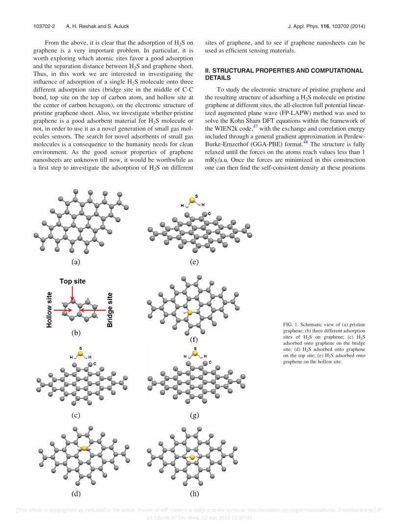
FIG. 1. Schematic view of (a) pristine
graphene; (b) three different adsorption
sites of H2S on graphene; (c) H2S
adsorbed onto graphene on the bridge
site; (d) H2S adsorbed onto graphene
on the top site; (e) H2S adsorbed onto
graphene on the hollow site.
103702-2 A. H. Reshak and S. Auluck J. Appl. Phys. 116, 103702 (2014)
[This article is copyrighted as indicated in the article. Reuse of AIP content is subject to the terms at: http://scitation.aip.org/termsconditions. Downloaded to ] IP:
14.139.60.97 On: Wed, 22 Apr 2015 10:57:03
by turning off the relaxations and driving the system to self-
consistency. From the obtained relaxed geometry, the elec-
tronic structure and the chemical bonding can be determined
and various spectroscopic features can be simulated and com-
pared with experimental data.
For the case of pristine graphene, we have studied three
possible adsorption sites namely; bridge site in which H2S
adsorbed in the middle of C-C bond with S-C separation dis-
tance 3.38 A (Fig. 1(c)), top site on the top of carbon atom
with S-C separation distance 3.36 A (Fig. 1(d)), and the hol-
low site at the center of the carbon hexagon with S-C separa-
tion distance 3.34 A (Fig. 1(e)).
In order to achieve the self-consistency, the values of
non-overlapping spheres of muffin-tin radius (RMT) as 1.33
a.u. for C at pristine graphene (4� 4) sheet, 1.27, 1.55, and
0.83 a.u. for C, S, and H atoms, respectively, at top-, bridge-,
and hollow-sites of adsorbed H2S onto graphene. These values
were chosen in such a way that the spheres did not overlap. In
order to achieve sufficient energy convergence, the wave-
functions in the interstitial regions were expanded in plane
waves with a cutoff Kmax¼ 7.0/RMT, where RMT denotes the
smallest atomic sphere radius and Kmax gives the magnitude
of the largest K vector in the plane wave basis expansion. The
maximum value of l was taken as lmax¼ 10, while the
charge density is Fourier expanded up to Gmax¼ 20 (a.u.)�1.
Self-consistency is obtained using 300 k-points in the irreduci-
ble Brillouin zone (IBZ). For calculating the total and the
angular momentum decomposition of the atoms projected
electronic density of states, a denser mesh of 800 k-points was
used. The self-consistent calculations are considered to be
converged when the total energy of the system is stable within
10�5 Ry.
FIG. 2. Calculated electronic band structure.
103702-3 A. H. Reshak and S. Auluck J. Appl. Phys. 116, 103702 (2014)
[This article is copyrighted as indicated in the article. Reuse of AIP content is subject to the terms at: http://scitation.aip.org/termsconditions. Downloaded to ] IP:
14.139.60.97 On: Wed, 22 Apr 2015 10:57:03
III. RESULTS AND DISCUSSION
A. Electronic band structure, density of states,and electronic charge density
The geometry of the atomic configurations of pristine gra-
phene (Fig. 1(a)) and three possible adsorption sites of H2S sin-
gle molecule onto pristine graphene: bridge site (Figs. 1(b) and
1(c)), top site (Figs. 1(b) and 1(d)), and the hollow site (Figs.
1(b) and 1(e)) were used in this study. We should emphasize
that the most stable adsorption configuration is the one with
the lowest total energy and the highest adsorption energy
among other adsorption sites.49 Thus, the top site (total energy
ETOT¼�3238.87878541 Ryd) is the most stable configuration
in comparison to hollow (ETOT¼�3238.1058284 Ryd) and
bridge (ETOT¼�3238.79501144 Ryd).
In Figs. 2(a)–2(d), we have plotted the electronic band
structure dispersion of the pristine graphene sheet and the
three structures (top, bridge, and hollow) in k-space along
the high symmetry directions in the irreducible Brillouin
zone. Following these figures, one can notice that adsorbed
H2S onto pristine graphene results in change of the electronic
band structure. For example, adsorption of H2S onto bridge
site causes a dramatic change of the band dispersions
(Fig. 2(b)) with respect to pristine graphene (Fig. 2(a)) and
opens a direct small energy gap of about 0.1 eV around
Fermi energy (EF) at M point of BZ. This is attributed to the
fact that adsorbed H2S on bridge site causes strong hybrid-
ization between C-p and H-s, S-s/p states at the valence band
maximum (VBM) and hence strong covalent bonds, while at
the conduction band minimum (CBM) the hybridization is
weaker and the bonds too. Also, the Coulomb interaction
between H2S and the two C atoms is weak; the states around
EF repel each others, causing to push the CBM towards
higher energy with respect to EF opening a direct gap. While
adsorbing H2S on the top site causes to push CBM further
towards higher energies resulting in a direct energy band gap
of about 0.3 eV around K point of BZ (Fig. 2(c)). Adsorbing
H2S on top site causes very strong hybridization between
C-p and H-s, S-s/p states at the VBM resulting in very strong
covalent bonds, while at the CBM the hybridization is much
weaker which leads to weak bonds and very weak Coulomb
interaction between H2S and the one C atom resulting in
strong repulsion between the states around EF, thus causing
to push the CBM further towards higher energy with respect
to EF opening a slightly bigger direct gap. The upper valence
band (Figs. 2(a)–2(d)) shows a very flat k-dispersion.
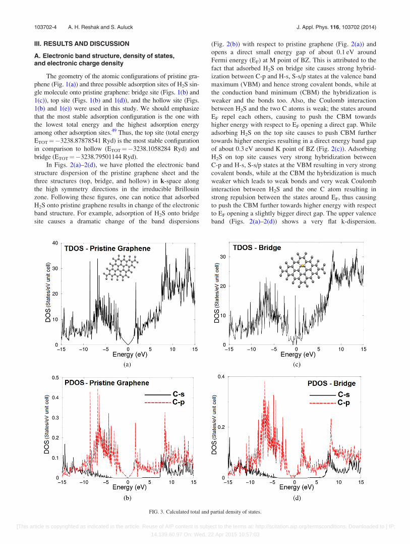
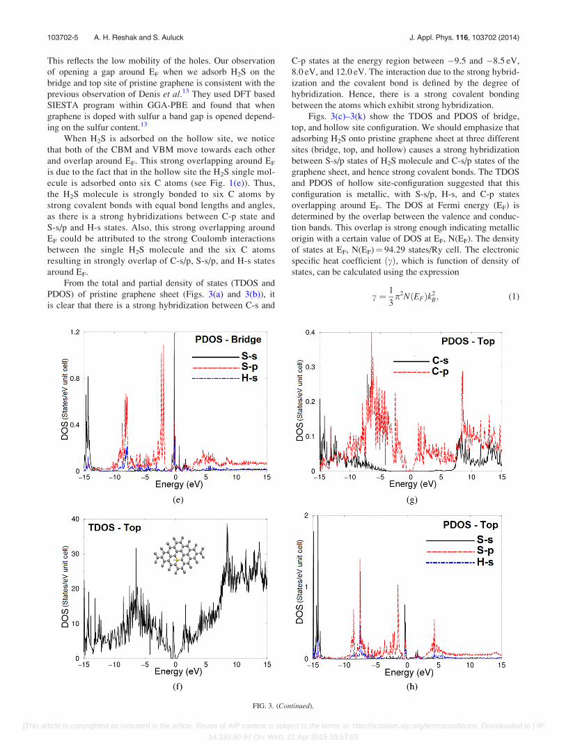
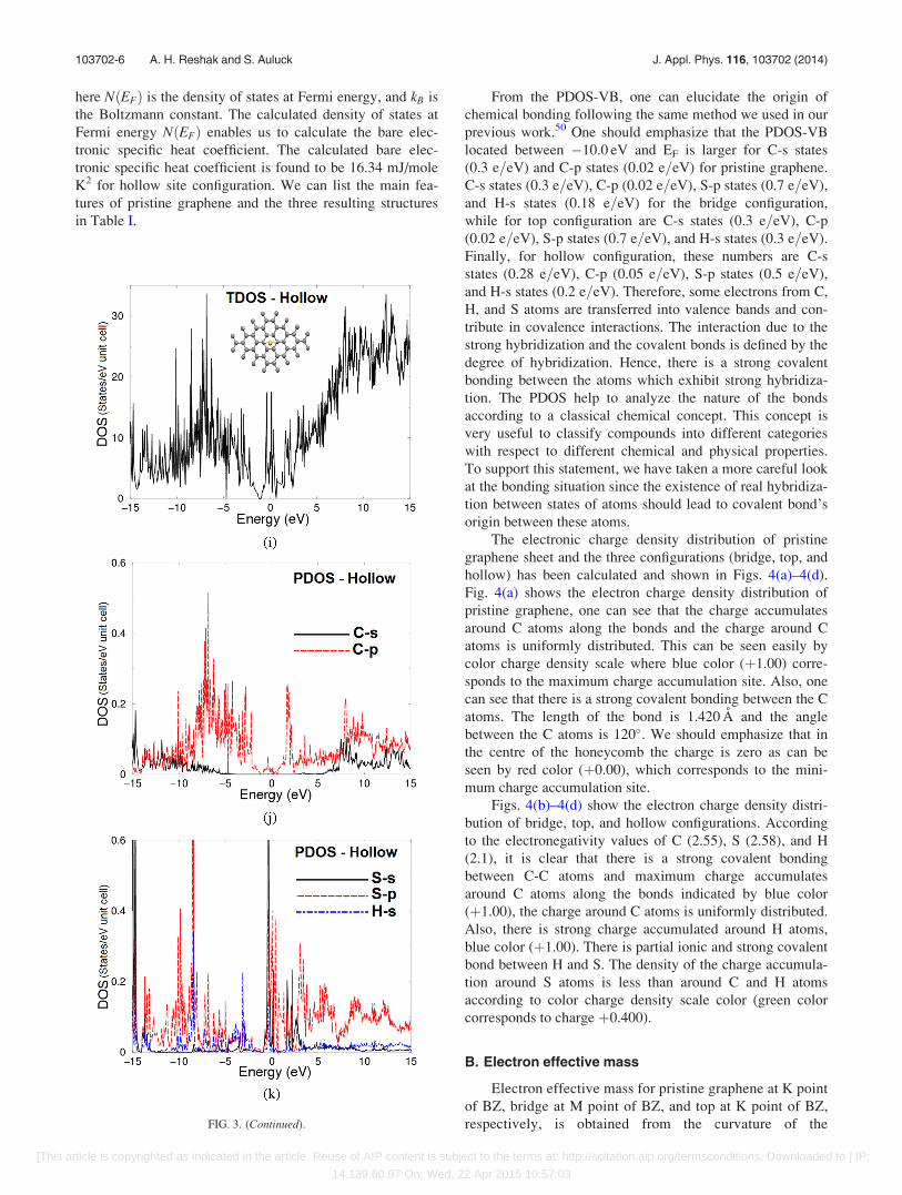
FIG. 3. Calculated total and partial density of states.
103702-4 A. H. Reshak and S. Auluck J. Appl. Phys. 116, 103702 (2014)
[This article is copyrighted as indicated in the article. Reuse of AIP content is subject to the terms at: http://scitation.aip.org/termsconditions. Downloaded to ] IP:
14.139.60.97 On: Wed, 22 Apr 2015 10:57:03
This reflects the low mobility of the holes. Our observation
of opening a gap around EF when we adsorb H2S on the
bridge and top site of pristine graphene is consistent with the
previous observation of Denis et al.13 They used DFT based
SIESTA program within GGA-PBE and found that when
graphene is doped with sulfur a band gap is opened depend-
ing on the sulfur content.13
When H2S is adsorbed on the hollow site, we notice
that both of the CBM and VBM move towards each other
and overlap around EF. This strong overlapping around EF
is due to the fact that in the hollow site the H2S single mol-
ecule is adsorbed onto six C atoms (see Fig. 1(e)). Thus,
the H2S molecule is strongly bonded to six C atoms by
strong covalent bonds with equal bond lengths and angles,
as there is a strong hybridizations between C-p state and
S-s/p and H-s states. Also, this strong overlapping around
EF could be attributed to the strong Coulomb interactions
between the single H2S molecule and the six C atoms
resulting in strongly overlap of C-s/p, S-s/p, and H-s states
around EF.
From the total and partial density of states (TDOS and
PDOS) of pristine graphene sheet (Figs. 3(a) and 3(b)), it
is clear that there is a strong hybridization between C-s and
C-p states at the energy region between �9.5 and �8.5 eV,
8.0 eV, and 12.0 eV. The interaction due to the strong hybrid-
ization and the covalent bond is defined by the degree of
hybridization. Hence, there is a strong covalent bonding
between the atoms which exhibit strong hybridization.
Figs. 3(c)–3(k) show the TDOS and PDOS of bridge,
top, and hollow site configuration. We should emphasize that
adsorbing H2S onto pristine graphene sheet at three different
sites (bridge, top, and hollow) causes a strong hybridization
between S-s/p states of H2S molecule and C-s/p states of the
graphene sheet, and hence strong covalent bonds. The TDOS
and PDOS of hollow site-configuration suggested that this
configuration is metallic, with S-s/p, H-s, and C-p states
overlapping around EF. The DOS at Fermi energy (EF) is
determined by the overlap between the valence and conduc-
tion bands. This overlap is strong enough indicating metallic
origin with a certain value of DOS at EF, N(EF). The density
of states at EF, N(EF)¼ 94.29 states/Ry cell. The electronic
specific heat coefficient ðcÞ, which is function of density of
states, can be calculated using the expression
c ¼ 1
3p2N EFð Þk2
B; (1)
FIG. 3. (Continued).
103702-5 A. H. Reshak and S. Auluck J. Appl. Phys. 116, 103702 (2014)
[This article is copyrighted as indicated in the article. Reuse of AIP content is subject to the terms at: http://scitation.aip.org/termsconditions. Downloaded to ] IP:
14.139.60.97 On: Wed, 22 Apr 2015 10:57:03
here NðEFÞ is the density of states at Fermi energy, and kB is
the Boltzmann constant. The calculated density of states at
Fermi energy NðEFÞ enables us to calculate the bare elec-
tronic specific heat coefficient. The calculated bare elec-
tronic specific heat coefficient is found to be 16.34 mJ/mole
K2 for hollow site configuration. We can list the main fea-
tures of pristine graphene and the three resulting structures
in Table I.
From the PDOS-VB, one can elucidate the origin of
chemical bonding following the same method we used in our
previous work.50 One should emphasize that the PDOS-VB
located between �10.0 eV and EF is larger for C-s states
(0.3 e=eV) and C-p states (0.02 e=eV) for pristine graphene.
C-s states (0.3 e=eV), C-p (0.02 e=eV), S-p states (0.7 e=eV),
and H-s states (0.18 e=eV) for the bridge configuration,
while for top configuration are C-s states (0.3 e=eV), C-p
(0.02 e=eV), S-p states (0.7 e=eV), and H-s states (0.3 e=eV).
Finally, for hollow configuration, these numbers are C-s
states (0.28 e=eV), C-p (0.05 e=eV), S-p states (0.5 e=eV),
and H-s states (0.2 e=eV). Therefore, some electrons from C,
H, and S atoms are transferred into valence bands and con-
tribute in covalence interactions. The interaction due to the
strong hybridization and the covalent bonds is defined by the
degree of hybridization. Hence, there is a strong covalent
bonding between the atoms which exhibit strong hybridiza-
tion. The PDOS help to analyze the nature of the bonds
according to a classical chemical concept. This concept is
very useful to classify compounds into different categories
with respect to different chemical and physical properties.
To support this statement, we have taken a more careful look
at the bonding situation since the existence of real hybridiza-
tion between states of atoms should lead to covalent bond’s
origin between these atoms.
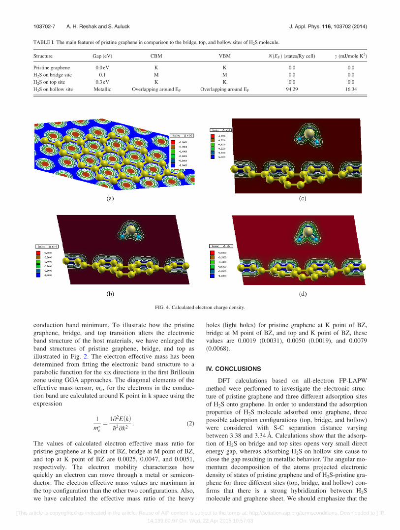
The electronic charge density distribution of pristine
graphene sheet and the three configurations (bridge, top, and
hollow) has been calculated and shown in Figs. 4(a)–4(d).
Fig. 4(a) shows the electron charge density distribution of
pristine graphene, one can see that the charge accumulates
around C atoms along the bonds and the charge around C
atoms is uniformly distributed. This can be seen easily by
color charge density scale where blue color (þ1.00) corre-
sponds to the maximum charge accumulation site. Also, one
can see that there is a strong covalent bonding between the C
atoms. The length of the bond is 1.420 A and the angle
between the C atoms is 120�. We should emphasize that in
the centre of the honeycomb the charge is zero as can be
seen by red color (þ0.00), which corresponds to the mini-
mum charge accumulation site.
Figs. 4(b)–4(d) show the electron charge density distri-
bution of bridge, top, and hollow configurations. According
to the electronegativity values of C (2.55), S (2.58), and H
(2.1), it is clear that there is a strong covalent bonding
between C-C atoms and maximum charge accumulates
around C atoms along the bonds indicated by blue color
(þ1.00), the charge around C atoms is uniformly distributed.
Also, there is strong charge accumulated around H atoms,
blue color (þ1.00). There is partial ionic and strong covalent
bond between H and S. The density of the charge accumula-
tion around S atoms is less than around C and H atoms
according to color charge density scale color (green color
corresponds to charge þ0.400).
B. Electron effective mass
Electron effective mass for pristine graphene at K point
of BZ, bridge at M point of BZ, and top at K point of BZ,
respectively, is obtained from the curvature of theFIG. 3. (Continued).
103702-6 A. H. Reshak and S. Auluck J. Appl. Phys. 116, 103702 (2014)
[This article is copyrighted as indicated in the article. Reuse of AIP content is subject to the terms at: http://scitation.aip.org/termsconditions. Downloaded to ] IP:
14.139.60.97 On: Wed, 22 Apr 2015 10:57:03
conduction band minimum. To illustrate how the pristine
graphene, bridge, and top transition alters the electronic
band structure of the host materials, we have enlarged the
band structures of pristine graphene, bridge, and top as
illustrated in Fig. 2. The electron effective mass has been
determined from fitting the electronic band structure to a
parabolic function for the six directions in the first Brillouin
zone using GGA approaches. The diagonal elements of the
effective mass tensor, me, for the electrons in the conduc-
tion band are calculated around K point in k space using the
expression
1
m�e¼ 1@2E kð Þ
�h2@k2: (2)
The values of calculated electron effective mass ratio for
pristine graphene at K point of BZ, bridge at M point of BZ,
and top at K point of BZ are 0.0025, 0.0047, and 0.0051,
respectively. The electron mobility characterizes how
quickly an electron can move through a metal or semicon-
ductor. The electron effective mass values are maximum in
the top configuration than the other two configurations. Also,
we have calculated the effective mass ratio of the heavy
holes (light holes) for pristine graphene at K point of BZ,
bridge at M point of BZ, and top and K point of BZ, these
values are 0.0019 (0.0031), 0.0050 (0.0019), and 0.0079
(0.0068).
IV. CONCLUSIONS
DFT calculations based on all-electron FP-LAPW
method were performed to investigate the electronic struc-
ture of pristine graphene and three different adsorption sites
of H2S onto graphene. In order to understand the adsorption
properties of H2S molecule adsorbed onto graphene, three
possible adsorption configurations (top, bridge, and hollow)
were considered with S-C separation distance varying
between 3.38 and 3.34 A. Calculations show that the adsorp-
tion of H2S on bridge and top sites opens very small direct
energy gap, whereas adsorbing H2S on hollow site cause to
close the gap resulting in metallic behavior. The angular mo-
mentum decomposition of the atoms projected electronic
density of states of pristine graphene and of H2S-pristine gra-
phene for three different sites (top, bridge, and hollow) con-
firms that there is a strong hybridization between H2S
molecule and graphene sheet. We should emphasize that the
TABLE I. The main features of pristine graphene in comparison to the bridge, top, and hollow sites of H2S molecule.
Structure Gap (eV) CBM VBM NðEFÞ (states/Ry cell) c (mJ/mole K2)
Pristine graphene 0.0 eV K K 0.0 0.0
H2S on bridge site 0.1 M M 0.0 0.0
H2S on top site 0.3 eV K K 0.0 0.0
H2S on hollow site Metallic Overlapping around EF Overlapping around EF 94.29 16.34
FIG. 4. Calculated electron charge density.
103702-7 A. H. Reshak and S. Auluck J. Appl. Phys. 116, 103702 (2014)
[This article is copyrighted as indicated in the article. Reuse of AIP content is subject to the terms at: http://scitation.aip.org/termsconditions. Downloaded to ] IP:
14.139.60.97 On: Wed, 22 Apr 2015 10:57:03
strong hybridization between H2S molecule and pristine gra-
phene sheet results in dramatic changes in the electronic
properties. Therefore, the interaction of H2S with graphene
shows very strong physical adsorption and hence different
physical properties. Thus, pristine graphene is very good ad-
sorbent materials for H2S molecule.
In summary, the pristine graphene sheet is a zero gap
semiconductor, while when a single H2S molecule adsorb
onto pristine graphene, we find that the bridge and top
become direct gap semiconductors (0.1 and 0.3 eV), whereas
the hollow case is metallic, where S-s/p, H-s, and C-p states
control the overlapping around EF. The DOS at EF is deter-
mined by the overlap between the valence and conduction
bands. This overlap is strong enough indicating metallic ori-
gin with certain value of DOS at EF, N(EF)¼ 94.29 states/Ry
cell, for hollow site configuration. The electronic specific
heat coefficient ðcÞ, which is function of DOS, can be
obtained from N(EF). Thus, the calculated bare electronic
specific heat coefficient is found to be 16.34 mJ/mole K2 for
hollow.
Adsorbing a single molecule of H2S onto pristine gra-
phene at the hollow sites causes change to pristine graphene
from zero-gap semiconductor to metallic with two bands
cuts Fermi level. Therefore, we have calculated the Fermi
surface of the new configuration. Fermi surface topology is
due to changes in inter-atomic distances, bonding angles as
well as to the degree of band filling.
ACKNOWLEDGMENTS
The result was developed within the CENTEM project,
Reg. No. CZ.1.05/2.1.00/03.0088, co-funded by the ERDF
as part of the Ministry of Education, Youth and Sports OP
RDI program. Computational resources were provided by
MetaCentrum (LM2010005) and CERIT-SC (CZ.1.05/
3.2.00/08.0144) infrastructures. S.A. thanks Council of
Scientific and Industrial Research (CSIR)-National Physical
Laboratory for financial support.
1K. Nakada, M. Fujita, G. Dresselhaus, and M. S. Dresselhaus, Phys. Rev.
B 54, 17954 (1996).2S. Okada, Phys. Rev. B 77, 041408 (2008).3R. Lv and M. Terrones, Mater. Lett. 78, 209–218 (2012).4C. Gomez-Navarro, M. Burghard, and K. Kern, Nano Lett. 8, 2045
(2008).5Y.-H. Lin, K. A. Jenkins, A. Valdes-Garcia, J. P. Small, D. B. Farmer, and
P. Avouris, Nano Lett. 9, 422 (2009).6C. L. Kane and E. J. Mele, Phys. Rev. Lett. 95, 226801 (2005).7A. Ferre-Vilaplana, J. Chem. Phys. 122, 104709 (2005).8I. Zanella, S. B. Fagan, R. Mota, and A. Fazzio, J. Phys. Chem. C 112,
9163 (2008).9Z. Liu, J. T. Robinson, X. Sun, and H. Dai, J. Am. Chem. Soc. 130, 10876
(2008).10A. de Leon and A. F. Jalbout, Chem. Phys. Lett. 457, 179 (2008).11R. M. Ribeiro, N. M. R. Peres, J. Coutinho, and P. R. Briddon, Phys. Rev.
B 78, 075442 (2008).12E. Bekyarova, M. E. Itkis, P. Ramesh, C. Berger, M. Sprinkle, W. A. De
Heer, and R. C. Haddon, J. Am. Chem. Soc. 131, 1336 (2009).13P. A. Denis, R. Faccio, and A. W. Mombru, ChemPhysChem 10, 715
(2009).14D. C. Elias, R. R. Nair, T. M. G. Mohiuddin, S. V. Morozov, P. Blake, M.
P. Halshall, A. C. Ferrari, D. W. Boukhvalov, M. I. Katsnelson, A. K.
Geim, and K. S. Novoselov, Science 323, 610 (2009).
15J. O. Sofo, A. S. Chaudhari, and G. D. Barber, Phys. Rev. B 75, 153401
(2007).16S. Casolo, O. L. Lovnik, R. Martinazzo, and G. F. Tantardini, J. Chem.
Phys. 130, 054704 (2009).17D. W. Boukhvalov, M. I. Katsnelson, and A. I. Lichtenstein, Phys. Rev. B
77, 035427 (2008).18X. Sha and B. Jackson, Surf. Sci. 496, 318 (2002).19L. Hornekaer, E. Rauls, W. Xu, Z. Sljivancanin, R. Otero, I. Steensgaard,
E. Laegsgaard, B. Hammer, and F. Besenbacher, Phys. Rev. Lett. 96,
156104 (2006).20Y. Ferro, F. Marinelli, and A. Allouche, Chem. Phys. Lett. 368, 609
(2003).21T. Roman, W. A. Dino, H. Nakanishi, H. Kasai, T. Sugimoto, and K.
Tange, Carbon 45, 218 (2007).22L. Chen, A. C. Copper, C. P. Pez, and H. Cheng, J. Phys. Chem. C 111,
18995 (2007).23P. O. Lehtinen, A. S. Foster, Y. Ma, A. V. Krasheninnikov, and R. M.
Nieminen, Phys. Rev. Lett. 93, 187202 (2004).24M. Suzuki, “Activated carbonfiber: Fundamentals and applications,”
Carbon 32, 577–586 (1994).25J. Zhao, A. Buldum, J. Han, and J. P. Lu, “Gas molecule adsorption in car-
bon nanotubes and nanotube bundles,” Nanotechnology 13, 195–200
(2002).26P. Bondavalli, P. Legagneux, and D. Pribat, “Carbon nanotubes based tran-
sistors as gas sensors: State of the art and critical review,” Sens. Actuators,
B 140, 304–318 (2009).27V. I. Hegde, S. N. Shirodkar, N. Tit, U. V. Waghmare, and Z. H. Yamani,
Surf. Sci. 621, 168–174 (2014).28J. M. Garcia-Lastra, D. J. Mowbray, K. S. Thygesen, A. Rubio, and K. W.
Jacobsen, “Computational design of chemical nanosensors: Metal doped
carbon nanotubes,” Phys. Rev. B 81, 245429 (2010).29J. E. Castellanos Aguila, H. Hernandez Cocoletzi, and G. Hernandez
Cocoletzi, AIP Adv. 3, 032118 (2013).30Y.-H. Zhang, L.-F. Han, Y.-H. Xiao, D.-Z. Ja, Z.-H. Guo, and F. Li,
Comput. Mater. Sci. 69, 222–228 (2013).31J. Kong et al., “Nanotube molecular wires as chemical sensors,” Science
287, 622–625 (2000).32P. G. Collins, K. Bradley, M. Ishigami, and A. Zettl, “Extreme oxygen
sensitivity of electronic properties of carbon nanotubes,” Science 287,
1801–1804 (2000).33F. Schedin, A. K. Geim, S. V. Morozov, E. W. Hill, P. Blake, M. I.
Katsnelson, and K. S. Novoselov, Nature Mater. 6, 652–655 (2007).34P. T. Moseley, “Solid state gas sensors,” Meas. Sci. Technol. 8, 223–237
(1997).35S. Capone, A. Forleo, L. Francioso, R. Rella, P. Siciliano, J.
Spadavecchia, D. S. Presicce, and A. M. Taurino, “Solid state gas sen-
sors: State of the art and future activities,” J. Optoelectron. Adv. Mater.
5, 1335–1348 (2003).36A. K. Geim and K. S. Novoselov, “The rise of grapheme,” Nature Mater.
6, 183–191 (2007).37K. S. Novoselov et al., “Two dimensional atomic crystals,” Proc. Natl.
Acad. Sci. U.S.A. 102, 10451–10453 (2005).38K. S. Novoselov et al., “Two dimensional gas of massless Dirac fermions
in graphene,” Nature 438, 197–200 (2005).39Y. Zhang, J. W. Tan, H. L. Stormer, and P. Kim, “Experimental observa-
tion of the quantum Hall effect and Berry’s phase in graphene,” Nature
438, 201–204 (2005).40P. Forzatti and L. Lietti, “Catalyst deactivation,” Catal. Today 52,
165–181 (1999).41Y. Xiao, Sh. Wang, D. Wu, and Q. Yuan, “Catalytic oxidation of hydrogen
sulfide over unmodified and impregnated activated carbon,” Sep. Purif.
Technol. 59, 326–332 (2008).42Y. Elsayed, M. Seredych, A. Dallas, and T. J. Bandosz, “Desulfurization
of air at high and low H2S concentrations,” Chem. Eng. J. 155, 594–602
(2009).43M. Darvish Ganji, N. Sharifi, M. Ardjmand, and M. Ghorbanzadeh
Ahangari, Appl. Surf. Sci. 261, 697–704 (2012).44P. Cosoli, M. Ferrone, S. Pricl, and M. Fermeglia, “Hydrogen sulphide re-
moval from biogas by zeolite adsorption. Part I. GCMC molecular simu-
lations,” Chem. Eng. J. 145, 86–92 (2008).45S. Mubeen, T. Zhang, N. Chartuprayoon, Y. Rheem, A. Mulchandani, N.
V. Myung, and M. A. Deshusses, “Sensitive detection of H2S using gold
nanoparticle decorated single-walled carbon nanotubes,” Anal. Chem. 82,
250–257 (2010).
103702-8 A. H. Reshak and S. Auluck J. Appl. Phys. 116, 103702 (2014)
[This article is copyrighted as indicated in the article. Reuse of AIP content is subject to the terms at: http://scitation.aip.org/termsconditions. Downloaded to ] IP:
14.139.60.97 On: Wed, 22 Apr 2015 10:57:03

46S. Nishimura and M. Yoda, “Removal of hydrogen sulfide from an anaer-
obic biogas using a bio-scrubber,” Water Sci. Technol. 36, 349–356
(1997).47P. Blaha, K. Schwarz, G. K. H. Madsen, D. Kvasnicka, and J. Luitz,
WIEN2K: An Augmented Plane Wave þ Local Orbitals Program forCalculating Crystal Properties (Techn. Universitat, Wien, Austria, 2001).
48J. P. Perdew, S. Burke, and M. Ernzerhof, Phys. Rev. Lett. 77, 3865–3868
(1996).49M. Zhou, Y.-H. Lu, Y.-Q. Cai, C. Zhang, and Y.-P. Feng, Nanotechnology
22, 385502 (2011).50A. H. Reshak, D. Stys, S. Auluck, and H. Kamarudin, Mater. Chem. Phys.
130, 458 (2011).
103702-9 A. H. Reshak and S. Auluck J. Appl. Phys. 116, 103702 (2014)
[This article is copyrighted as indicated in the article. Reuse of AIP content is subject to the terms at: http://scitation.aip.org/termsconditions. Downloaded to ] IP:
14.139.60.97 On: Wed, 22 Apr 2015 10:57:03