Embed Size (px)
Citation preview
1SLAU262D–January 2009–Revised February 2016Submit Documentation Feedback
Copyright © 2009–2016, Texas Instruments Incorporated
ADS79xxEVM and ADS79xxEVM-PDK
ADCPro is a trademark of Texas Instruments.Microsoft, Windows are registered trademarks of Microsoft Corporation.All other trademarks are the property of their respective owners.
User's GuideSLAU262D–January 2009–Revised February 2016
ADS79xxEVM and ADS79xxEVM-PDK
Figure 1. ADS7953EVM (Left) and ADS7953EVM-PDK (Right)
This users guide describes the characteristics, operation, and use of the ADS7953EVM, ADS7957EVMand ADS7961EVM, both by themselves and as part of the ADS7953EVM-PDK, ADS7957EVM-PDK orADS7961EVM-PDK. These evaluation modules (EVMs) are evaluation boards for the ADS7953, a 12-bit,16-channel, successive approximation register (SAR) analog-to-digital converter (ADC), and the ADS7957and ADS7961, which are 10-bit and 8-bit variations of the ADS7953. The EVM allows evaluation of allaspects of the ADS7953, ADS7957 or ADS7961 device. Complete circuit descriptions, schematicdiagrams, and bills of material are included in this document.
The following related documents are available through the Texas Instruments website at http://www.ti.com.
www.ti.com
2 SLAU262D–January 2009–Revised February 2016Submit Documentation Feedback
Copyright © 2009–2016, Texas Instruments Incorporated
ADS79xxEVM and ADS79xxEVM-PDK
Contents1 EVM Overview ............................................................................................................... 32 Analog Interface.............................................................................................................. 43 Digital Interface .............................................................................................................. 54 Power Supplies .............................................................................................................. 65 Voltage Reference ........................................................................................................... 66 EVM Operation............................................................................................................... 67 ADS7953EVM-PDK Kit Operation ......................................................................................... 88 Evaluating Performance with the ADCPro Software................................................................... 199 Schematic and Bill of Materials........................................................................................... 26
List of Figures
1 ADS7953EVM (Left) and ADS7953EVM-PDK (Right) .................................................................. 12 ADS7953EVM Default Jumper Locations ................................................................................ 73 MMB0 Initial Setup........................................................................................................... 94 Connecting an External Power Supply ................................................................................. 105 Laboratory Power-Supply Connection................................................................................... 116 NI-VISA Driver Installation ................................................................................................ 127 NI-VISA Driver Installation Question .................................................................................... 128 NI-VISA Driver Installing .................................................................................................. 139 NI-VISA Driver Complete Installation ................................................................................... 1310 NI-VISA Driver Verification Using Device Manager ................................................................... 1411 ADCPro Software Start-up Display Window ............................................................................ 1412 ADS7953EVM-PDK Plug-In Display Window........................................................................... 1513 Install New Driver Wizard Screen 1...................................................................................... 1614 Install New Driver Wizard Screen 2...................................................................................... 1615 Install New Driver Wizard Screen 3...................................................................................... 1716 Install New Driver Wizard Screen 4...................................................................................... 1717 Install New Driver Wizard Screen 5...................................................................................... 1818 USBSytx Driver Verification Using Device Manager .................................................................. 1819 Channel Enable............................................................................................................. 2020 Manual Channel Control................................................................................................... 2121 Serial Clock, Input Range and MS Nibble settings .................................................................... 2222 High and Low Alarm Limits by Channel ................................................................................. 2323 GPIO and System Monitor Control options ............................................................................. 2424 GPIO selection, controls and indicators ................................................................................. 2525 Progress Bar While Collecting Data ..................................................................................... 2626 ADS7953EVM Schematic ................................................................................................. 27
List of Tables
1 EVM-Compatible Device Data Sheets .................................................................................... 32 Primary Analog Interface Pinout ........................................................................................... 43 Secondary Analog Interface Pinout ....................................................................................... 44 Serial Interface Pins ......................................................................................................... 55 P3 Configuration: Power-Supply Input .................................................................................... 66 List of Jumpers ............................................................................................................... 77 ADS7953EVM Bill of Materials ........................................................................................... 28
www.ti.com EVM Overview
3SLAU262D–January 2009–Revised February 2016Submit Documentation Feedback
Copyright © 2009–2016, Texas Instruments Incorporated
ADS79xxEVM and ADS79xxEVM-PDK
1 EVM Overview
Table 1. EVM-Compatible Device Data Sheets
Device Literature NumberADS7953, ADS7952, ADS7951, ADS7950, ADS7957, ADS7956,ADS7955, ADS7954, ADS7961, ADS7960, ADS7959, ADS7958 SLAS605
OPA365 SBOS365REF5025 SBOS410
1.1 FeaturesADS7953EVM/ADS7957EVM/ADS7961 EVM Features:• Contains all support circuitry needed for the ADS7953/ADS7957/ADS7961• Voltage reference options: external or onboard• Buffer options: onboard analog input buffer can be bypassed• GPIO access with HI or LO alarm options to interrupt host processor• Compatible with the TI Modular EVM System
ADS7953EVM/ADS7957EVM/ADS7961EVM-PDK Features:• Easy-to-use evaluation software for Microsoft® Windows® XP• Data collection to text files• Built-in analysis tools including scope, FFT, and histogram displays• Complete control of board settings• Easily expandable with new analysis plug-in tools from Texas Instruments
For use with a computer, the ADS79xxEVM Performance Demonstration Kit (PDK) is available. This kitcombines the ADS7953EVM, ADS7957EVM or ADS7961EVM board with the TMS320VC5507 DSP-based MMB0 motherboard, and includes ADCPro™ software for evaluation.
The MMB0 motherboard allows the ADS79xxEVM to be connected to the computer via an available USBport. This manual shows how to use the MMB0 as part of the ADS79xxEVM-PDK, but does not providetechnical details about the MMB0 itself.
ADCPro is a program for collecting, recording, and analyzing data from ADC evaluation boards. It is basedon a number of plug-in programs, so it can be expanded easily with new test and data collection plug-ins.The ADS79xxEVM-PDK is controlled by a plugin running in ADCPro. For more information about ADCPro,see the ADCPro Analog-to-Digital Converter Evalutation Software Users Guide, available for downloadfrom the TI website.
This manual covers the operation of all three ADS7953, ADS7957 and ADS7961 devices refered to as theADS79xxEVM and the ADS79xxEVM-PDK. Throughout this document, the abbreviation EVM and the termevaluation module are synonymous with the ADS79xxEVM. For clarity of reading, the rest of this manualwill refer only to the ADS7953EVM or ADS7953EVM-PDK. The individual kit contains one ADS7953EVM,ADS7957EVM or ADS7961EVM, but operation of the EVM and kit for the ADS7957 or ADS7961 isidentical, unless otherwise noted.
1.2 IntroductionThe ADS7953EVM is an evaluation module built to the TI Modular EVM System specification. It can beconnected to any of the modular EVM system interface cards available from Texas Instruments.
The ADS7953EVM is available as a stand-alone printed circuit board (PCB) or as part of theADS7953EVM-PDK, which includes an MMB0 motherboard and software. As a stand-alone PCB, theADS7953EVM is useful for prototyping designs and firmware.
Note that the ADS7953EVM has no microprocessor and cannot run software. To connect it to a computer,some type of host processor interface capable of generating the necessary control signals is required.
Analog Interface www.ti.com
4 SLAU262D–January 2009–Revised February 2016Submit Documentation Feedback
Copyright © 2009–2016, Texas Instruments Incorporated
ADS79xxEVM and ADS79xxEVM-PDK
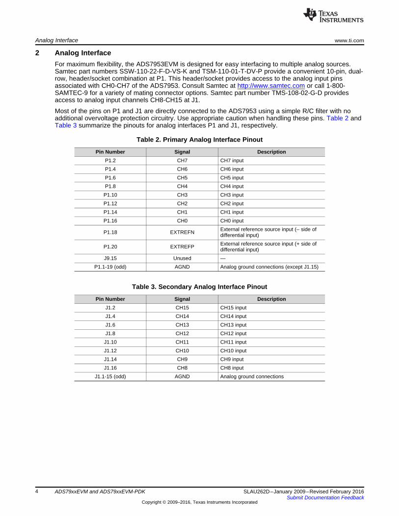
2 Analog InterfaceFor maximum flexibility, the ADS7953EVM is designed for easy interfacing to multiple analog sources.Samtec part numbers SSW-110-22-F-D-VS-K and TSM-110-01-T-DV-P provide a convenient 10-pin, dual-row, header/socket combination at P1. This header/socket provides access to the analog input pinsassociated with CH0-CH7 of the ADS7953. Consult Samtec at http://www.samtec.com or call 1-800-SAMTEC-9 for a variety of mating connector options. Samtec part number TMS-108-02-G-D providesaccess to analog input channels CH8-CH15 at J1.
Most of the pins on P1 and J1 are directly connected to the ADS7953 using a simple R/C filter with noadditional overvoltage protection circuitry. Use appropriate caution when handling these pins. Table 2 andTable 3 summarize the pinouts for analog interfaces P1 and J1, respectively.
Table 2. Primary Analog Interface Pinout
Pin Number Signal DescriptionP1.2 CH7 CH7 inputP1.4 CH6 CH6 inputP1.6 CH5 CH5 inputP1.8 CH4 CH4 input
P1.10 CH3 CH3 inputP1.12 CH2 CH2 inputP1.14 CH1 CH1 inputP1.16 CH0 CH0 input
P1.18 EXTREFN External reference source input (– side ofdifferential input)
P1.20 EXTREFP External reference source input (+ side ofdifferential input)
J9.15 Unused —P1.1-19 (odd) AGND Analog ground connections (except J1.15)
Table 3. Secondary Analog Interface Pinout
Pin Number Signal DescriptionJ1.2 CH15 CH15 inputJ1.4 CH14 CH14 inputJ1.6 CH13 CH13 inputJ1.8 CH12 CH12 inputJ1.10 CH11 CH11 inputJ1.12 CH10 CH10 inputJ1.14 CH9 CH9 inputJ1.16 CH8 CH8 input
J1.1-15 (odd) AGND Analog ground connections
www.ti.com Digital Interface
5SLAU262D–January 2009–Revised February 2016Submit Documentation Feedback
Copyright © 2009–2016, Texas Instruments Incorporated
ADS79xxEVM and ADS79xxEVM-PDK
3 Digital Interface
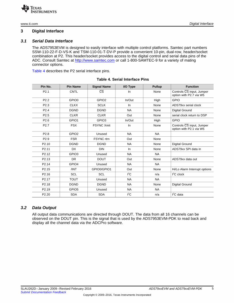
3.1 Serial Data InterfaceThe ADS7953EVM is designed to easily interface with multiple control platforms. Samtec part numbersSSW-110-22-F-D-VS-K and TSM-110-01-T-DV-P provide a convenient 10-pin, dual-row, header/socketcombination at P2. This header/socket provides access to the digital control and serial data pins of theADC. Consult Samtec at http://www.samtec.com or call 1-800-SAMTEC-9 for a variety of matingconnector options.
Table 4 describes the P2 serial interface pins.
Table 4. Serial Interface Pins
Pin No. Pin Name Signal Name I/O Type Pullup FunctionP2.1 CNTL CS In None Controls CS input, Jumper
option with P2.7 via W5P2.2 GPIO0 GPIO2 In/Out High GPIOP2.3 CLKX SCLK In None ADS79xx serial clockP2.4 DGND DGND NA None Digital GroundP2.5 CLKR CLKR Out None serial clock return to DSPP2.6 GPIO1 GPIO3 In/Out High GPIOP2.7 FSX FSYNC Xmit In None Controls CS input, Jumper
option with P2.1 via W5P2.8 GPIO2 Unused NA NAP2.9 FSR FSYNC rtrn Out NoneP2.10 DGND DGND NA None Digital GroundP2.11 DX DIN In None ADS79xx SPI data inP2.12 GPIO3 Unused NA NAP2.13 DR DOUT Out None ADS79xx data outP2.14 GPIO4 Unused NA NAP2.15 /INT GPIO0/GPIO1 Out None Hi/Lo Alarm Interrupt optionsP2.16 SCL SCL I2C n/a I2C clockP2.17 TOUT Unused NA NAP2.18 DGND DGND NA None Digital GroundP2.19 GPIO5 Unused NA NAP2.20 SDA SDA I2C n/a I2C data
3.2 Data OutputAll output data communications are directed through DOUT. The data from all 16 channels can beobserved on the DOUT pin. This is the signal that is used by the ADS7953EVM-PDK to read back anddisplay all the channel data via the ADCPro software.
Power Supplies www.ti.com
6 SLAU262D–January 2009–Revised February 2016Submit Documentation Feedback
Copyright © 2009–2016, Texas Instruments Incorporated
ADS79xxEVM and ADS79xxEVM-PDK
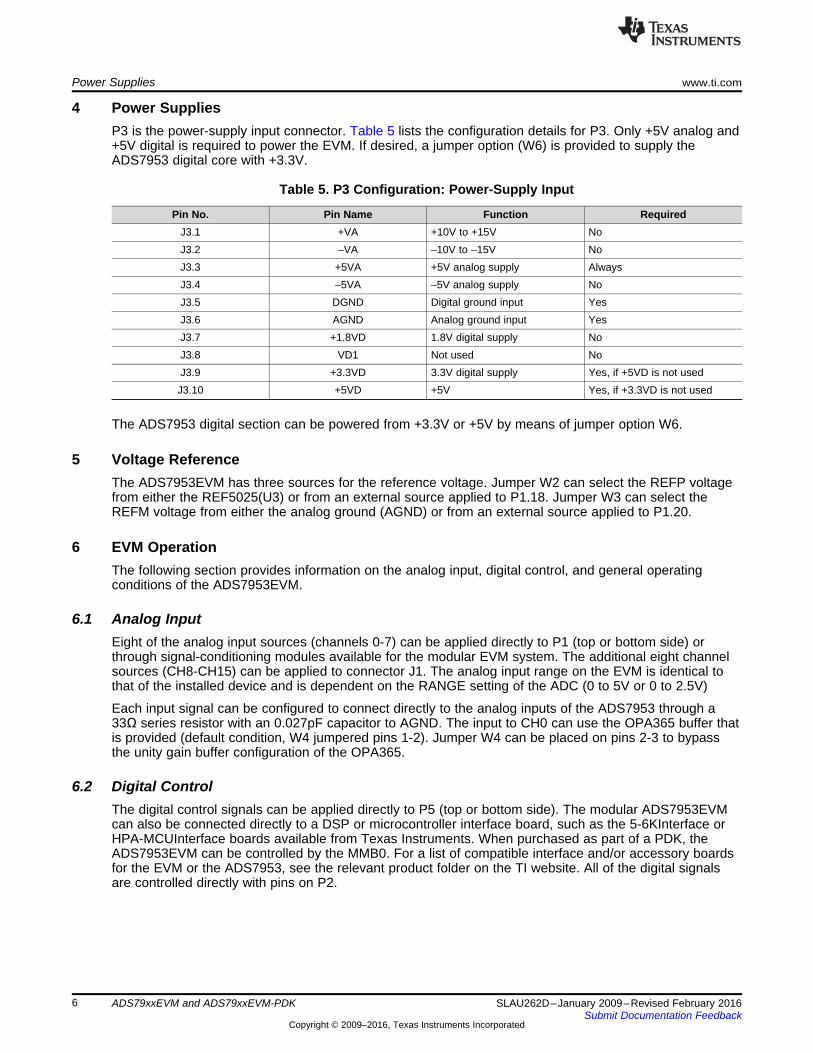
4 Power SuppliesP3 is the power-supply input connector. Table 5 lists the configuration details for P3. Only +5V analog and+5V digital is required to power the EVM. If desired, a jumper option (W6) is provided to supply theADS7953 digital core with +3.3V.
Table 5. P3 Configuration: Power-Supply Input
Pin No. Pin Name Function RequiredJ3.1 +VA +10V to +15V NoJ3.2 –VA –10V to –15V NoJ3.3 +5VA +5V analog supply AlwaysJ3.4 –5VA –5V analog supply NoJ3.5 DGND Digital ground input YesJ3.6 AGND Analog ground input YesJ3.7 +1.8VD 1.8V digital supply NoJ3.8 VD1 Not used NoJ3.9 +3.3VD 3.3V digital supply Yes, if +5VD is not usedJ3.10 +5VD +5V Yes, if +3.3VD is not used
The ADS7953 digital section can be powered from +3.3V or +5V by means of jumper option W6.
5 Voltage ReferenceThe ADS7953EVM has three sources for the reference voltage. Jumper W2 can select the REFP voltagefrom either the REF5025(U3) or from an external source applied to P1.18. Jumper W3 can select theREFM voltage from either the analog ground (AGND) or from an external source applied to P1.20.
6 EVM OperationThe following section provides information on the analog input, digital control, and general operatingconditions of the ADS7953EVM.
6.1 Analog InputEight of the analog input sources (channels 0-7) can be applied directly to P1 (top or bottom side) orthrough signal-conditioning modules available for the modular EVM system. The additional eight channelsources (CH8-CH15) can be applied to connector J1. The analog input range on the EVM is identical tothat of the installed device and is dependent on the RANGE setting of the ADC (0 to 5V or 0 to 2.5V)
Each input signal can be configured to connect directly to the analog inputs of the ADS7953 through a33Ω series resistor with an 0.027pF capacitor to AGND. The input to CH0 can use the OPA365 buffer thatis provided (default condition, W4 jumpered pins 1-2). Jumper W4 can be placed on pins 2-3 to bypassthe unity gain buffer configuration of the OPA365.
6.2 Digital ControlThe digital control signals can be applied directly to P5 (top or bottom side). The modular ADS7953EVMcan also be connected directly to a DSP or microcontroller interface board, such as the 5-6KInterface orHPA-MCUInterface boards available from Texas Instruments. When purchased as part of a PDK, theADS7953EVM can be controlled by the MMB0. For a list of compatible interface and/or accessory boardsfor the EVM or the ADS7953, see the relevant product folder on the TI website. All of the digital signalsare controlled directly with pins on P2.
www.ti.com EVM Operation
7SLAU262D–January 2009–Revised February 2016Submit Documentation Feedback
Copyright © 2009–2016, Texas Instruments Incorporated
ADS79xxEVM and ADS79xxEVM-PDK
6.3 ADS7953EVM-PDK Power SupplyThe analog portion of the ADS7953EVM can either be powered by a 5V source generated via an externalpower supply using the included CA-2186 cable or by applying the +5VA to the connector on the MMB0board. The MMB0 board will provide the digital 5V and 3.3V to the ADS7953EVM. To provide +5VA to theADS7953EVM from the MMB0 board, make sure the jumper at J13 (on the MMB0) is closed from +5V to+5VA.
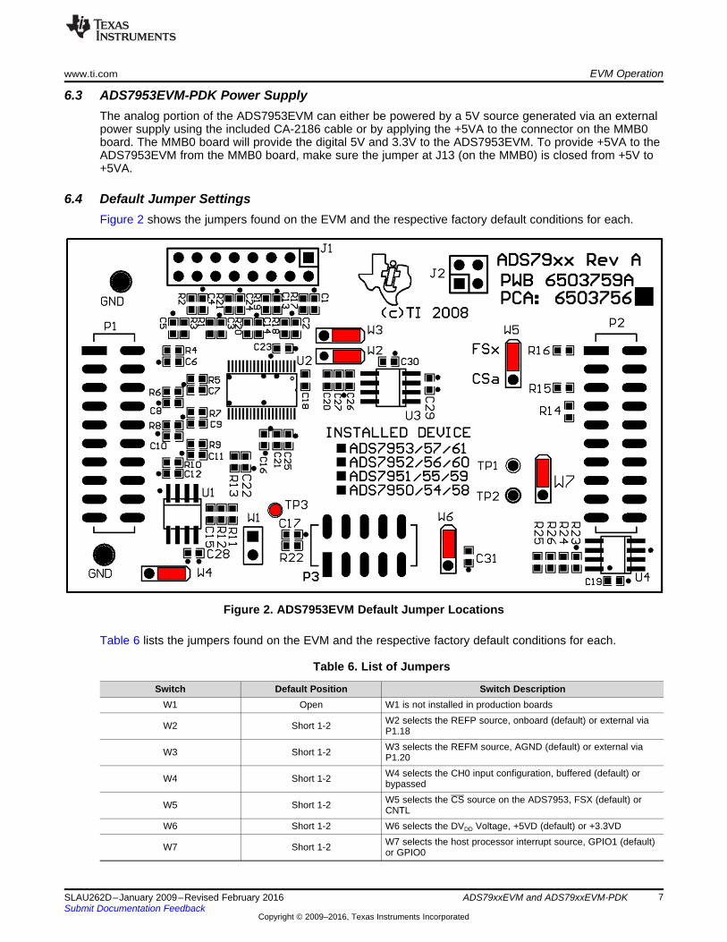
6.4 Default Jumper SettingsFigure 2 shows the jumpers found on the EVM and the respective factory default conditions for each.
Figure 2. ADS7953EVM Default Jumper Locations
Table 6 lists the jumpers found on the EVM and the respective factory default conditions for each.
Table 6. List of Jumpers
Switch Default Position Switch DescriptionW1 Open W1 is not installed in production boards
W2 Short 1-2 W2 selects the REFP source, onboard (default) or external viaP1.18
W3 Short 1-2 W3 selects the REFM source, AGND (default) or external viaP1.20
W4 Short 1-2 W4 selects the CH0 input configuration, buffered (default) orbypassed
W5 Short 1-2 W5 selects the CS source on the ADS7953, FSX (default) orCNTL
W6 Short 1-2 W6 selects the DVDD Voltage, +5VD (default) or +3.3VD
W7 Short 1-2 W7 selects the host processor interrupt source, GPIO1 (default)or GPIO0
ADS7953EVM-PDK Kit Operation www.ti.com
8 SLAU262D–January 2009–Revised February 2016Submit Documentation Feedback
Copyright © 2009–2016, Texas Instruments Incorporated
ADS79xxEVM and ADS79xxEVM-PDK
7 ADS7953EVM-PDK Kit OperationThis section provides information on using the ADS7953EVM-PDK, including setup, program installation,and program usage.
To prepare to evaluate the ADS7953 with the ADS7953EVM-PDK, complete the following steps:
Step 1. Install the ADCPro software (if not already installed) on a PC.
Step 2. Install the ADS7953EVM-PDK EVM plug-in software.
Step 3. Set up the ADS7953EVM-PDK.
Step 4. Connect a proper power supply.
Step 5. Complete the NI-VISA USB driver installation process.
Step 6. Run the ADCPro software.
Step 7. Complete the Microsoft Windows USB driver installation process.
Each task is described in the subsequent sections of this document.
7.1 Installing the ADCPro Software
CAUTIONDo not connect the ADS7953EVM-PDK before installing the software on asuitable PC. Failure to observe this caution may cause Microsoft Windows tonot recognize the ADS7953EVM-PDK.
The latest software is available from the TI website at http://www.ti.com/. The ADCPro installer will checkfor updates when executed (if connected to the Internet), and then gives the option of downloading andinstalling the latest version. See the ADCPro Analog-to-Digital Converter Evalutation Software UsersGuide for instructions on installing and using ADCPro.
To install the ADS7953EVM-PDK plug-in, run the file: ads7953evm-pdk-plugin-1.1.0.exe (1.1.0 is theversion number, and increments with software version releases). Double-click the file to run it; then followthe instructions shown. Also, use the ADCPro Update Check feature to check for newer versions of theADS7953EVM-PDK plug-in, once one version has been installed.
The software should now be installed, but the USB drivers may not have been loaded by the PC operatingsystem. This step will complete when the ADCPro software is executed.
7.2 Setting Up the ADS7953EVM-PDKThe ADS7953EVM-PDK contains both the ADS7953EVM and the MMB0 motherboard; however, thedevices are shipped unconnected. Follow these steps to set up the ADS7953EVM-PDK:
Step 1. Unpack the ADS7953EVM-PDK kit.
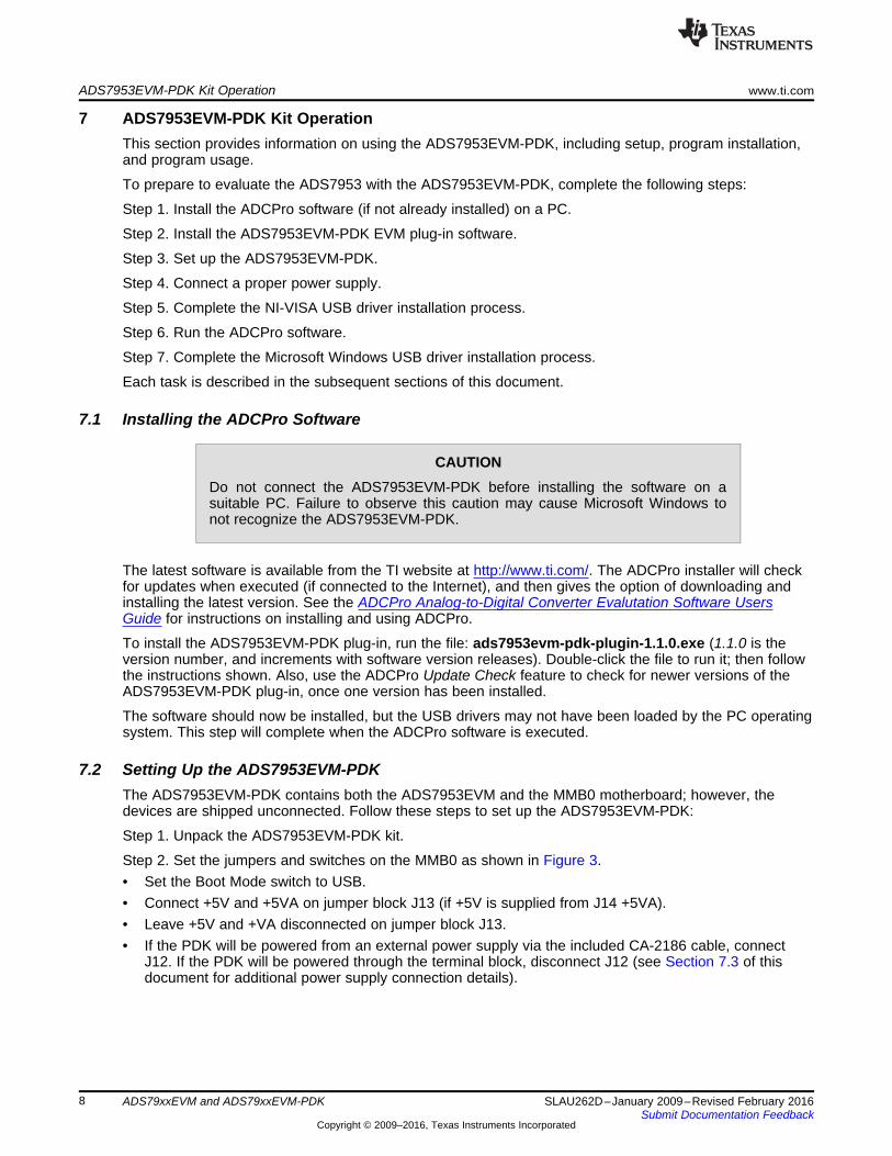
Step 2. Set the jumpers and switches on the MMB0 as shown in Figure 3.• Set the Boot Mode switch to USB.• Connect +5V and +5VA on jumper block J13 (if +5V is supplied from J14 +5VA).• Leave +5V and +VA disconnected on jumper block J13.• If the PDK will be powered from an external power supply via the included CA-2186 cable, connect
J12. If the PDK will be powered through the terminal block, disconnect J12 (see Section 7.3 of thisdocument for additional power supply connection details).
www.ti.com ADS7953EVM-PDK Kit Operation
9SLAU262D–January 2009–Revised February 2016Submit Documentation Feedback
Copyright © 2009–2016, Texas Instruments Incorporated
ADS79xxEVM and ADS79xxEVM-PDK
Figure 3. MMB0 Initial Setup
Step 3. Plug the ADS7953EVM into the MMB0. The female portion of P1, P2 and P3 on the EVM alignwith male connectors J7, J4 and J5 respective on the MMB0.
CAUTION Do not misalign the pins when plugging the ADS7953EVM into the MMB0. Check the pinalignment of P1, P2, and P3 carefully before applying power to the PDK.
Step 4. Verify the jumpers on the ADS7953EVM are as shown in Figure 2 (note that these settings are thefactory-configured settings for the EVM).
7.2.1 About the MMB0The MMB0 is a Modular EVM System motherboard. It is designed around the TMS320VC5507, a DSPwith an onboard USB interface from Texas Instruments. The MMB0 also has 16MB of SDRAM installed.
The MMB0 is not intended to be used as a DSP development board, and it is not available separately. TIcannot offer support for the MMB0 except as part of an EVM-PDK kit. For schematics or other informationabout the MMB0, contact Texas Instruments.
7.3 Connecting the Power SupplyThe ADS7953EVM-PDK can be operated with a unipolar +5V supply or a combination of +5V and +3.3Vsupplies.
When the MMB0 DSP is powered properly, LED D2 glows green. The green light indicates that the 3.3Vsupply for the MMB0 is operating properly. (It does not indicate that the EVM power supplies areoperating properly.)
ADS7953EVM-PDK Kit Operation www.ti.com
10 SLAU262D–January 2009–Revised February 2016Submit Documentation Feedback
Copyright © 2009–2016, Texas Instruments Incorporated
ADS79xxEVM and ADS79xxEVM-PDK
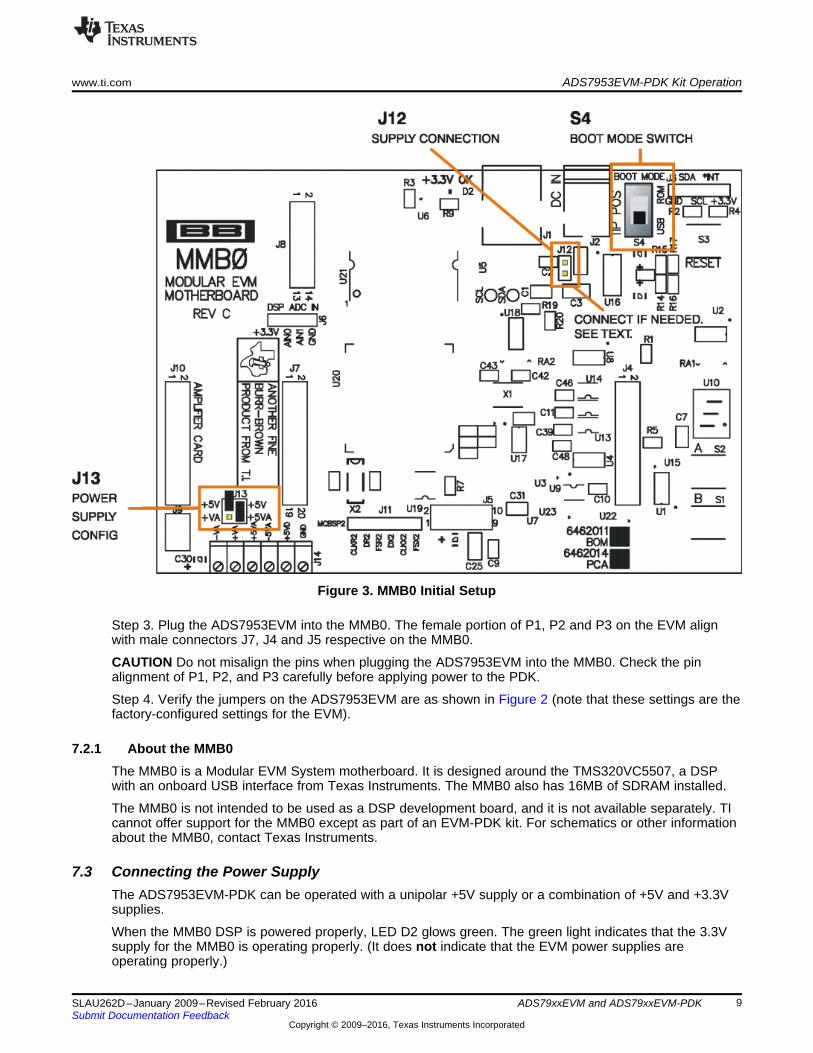
7.3.1 Connecting an External Power SupplyAn external power supply can be connected to barrel jack J2 on the MMB0. J2 is located next to the USBconnector. The external power supply must output 6V-7V dc. The connector must be sleeve-negative, tip-positive. It should have a current rating of at least 2A.
Jumper J12 on the MMB0 connects an external power supply to the board. To use the an external supply,J12 must be shorted. Figure 4 illustrates how to connect the included CA-2186 cable to the MMB0.
Figure 4. Connecting an External Power Supply
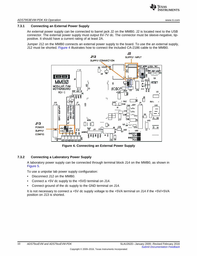
7.3.2 Connecting a Laboratory Power SupplyA laboratory power supply can be connected through terminal block J14 on the MMB0, as shown inFigure 5.
To use a unipolar lab power supply configuration:• Disconnect J12 on the MMB0.• Connect a +5V dc supply to the +5VD terminal on J14.• Connect ground of the dc supply to the GND terminal on J14.
It is not necessary to connect a +5V dc supply voltage to the +5VA terminal on J14 if the +5V/+5VAposition on J13 is shorted.
www.ti.com ADS7953EVM-PDK Kit Operation
11SLAU262D–January 2009–Revised February 2016Submit Documentation Feedback
Copyright © 2009–2016, Texas Instruments Incorporated
ADS79xxEVM and ADS79xxEVM-PDK
Figure 5. Laboratory Power-Supply Connection
7.4 Running the Software and Completing Driver InstallationNote: The software is continually under development. These instructions and screen images are current atthe time of this writing, but may not exactly match future releases.
The program for evaluating the ADS7953EVM-PDK is called ADCPro. This program uses plug-ins tocommunicate with the EVM. The ADS7953EVM-PDK plug-in is included in the ADS7953EVM-PDKpackage.
The program currently runs only on Microsoft Windows platforms of Windows XP; Windows Vista is NOTsupported at the time of this writing.
If this is the first time installing ADCPro and the EVM plug-ins, follow these procedures to run ADCPro andcomplete the necessary driver installation.
7.4.1 NI-VISA USB Device Driver Installation1. After the ADCPro software is installed, apply power to the PDK and connect the board to an available
PC USB port.2. The computer should recognize new hardware and begin installing the drivers for the hardware.
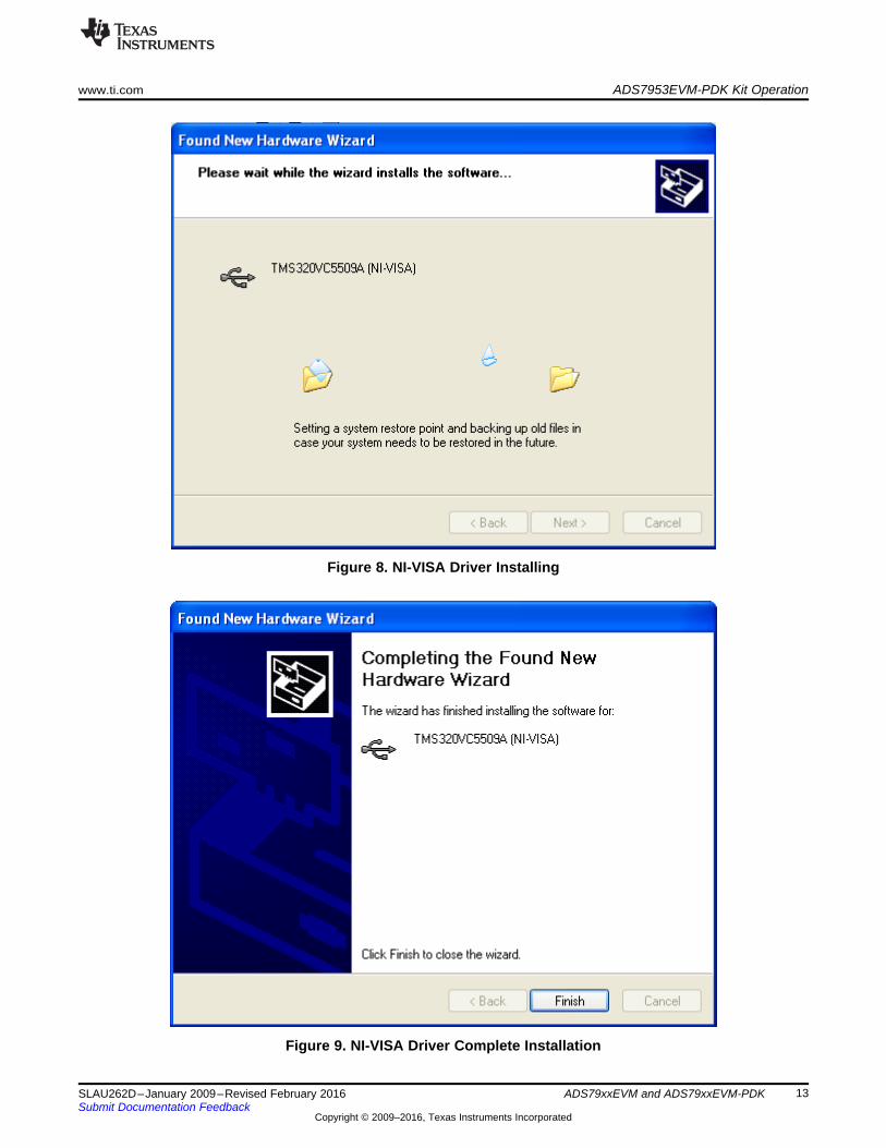
Figure 6 through Figure 10 are provided for reference to show the installation steps.• For the first screen, Figure 6, it is not necessary to search for the software; it has already been
installed to the PC.• For the remaining steps, accept the default settings.
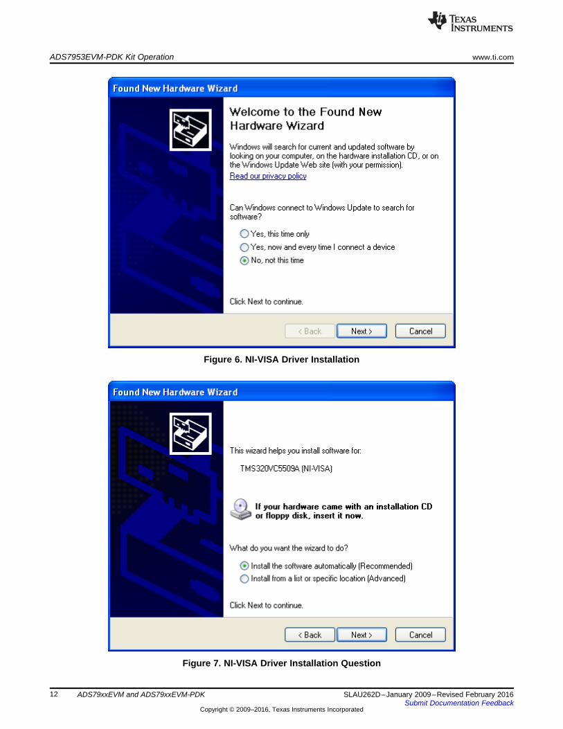
ADS7953EVM-PDK Kit Operation www.ti.com
12 SLAU262D–January 2009–Revised February 2016Submit Documentation Feedback
Copyright © 2009–2016, Texas Instruments Incorporated
ADS79xxEVM and ADS79xxEVM-PDK
Figure 6. NI-VISA Driver Installation
Figure 7. NI-VISA Driver Installation Question
www.ti.com ADS7953EVM-PDK Kit Operation
13SLAU262D–January 2009–Revised February 2016Submit Documentation Feedback
Copyright © 2009–2016, Texas Instruments Incorporated
ADS79xxEVM and ADS79xxEVM-PDK
Figure 8. NI-VISA Driver Installing
Figure 9. NI-VISA Driver Complete Installation
ADS7953EVM-PDK Kit Operation www.ti.com
14 SLAU262D–January 2009–Revised February 2016Submit Documentation Feedback
Copyright © 2009–2016, Texas Instruments Incorporated
ADS79xxEVM and ADS79xxEVM-PDK
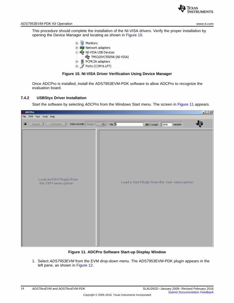
This procedure should complete the installation of the NI-VISA drivers. Verify the proper installation byopening the Device Manager and locating as shown in Figure 10.
Figure 10. NI-VISA Driver Verification Using Device Manager
Once ADCPro is installed, install the ADS7953EVM-PDK software to allow ADCPro to recognize theevaluation board.
7.4.2 USBStyx Driver InstallationStart the software by selecting ADCPro from the Windows Start menu. The screen in Figure 11 appears.
Figure 11. ADCPro Software Start-up Display Window
1. Select ADS7953EVM from the EVM drop-down menu. The ADS7953EVM-PDK plugin appears in theleft pane, as shown in Figure 12.
www.ti.com ADS7953EVM-PDK Kit Operation
15SLAU262D–January 2009–Revised February 2016Submit Documentation Feedback
Copyright © 2009–2016, Texas Instruments Incorporated
ADS79xxEVM and ADS79xxEVM-PDK
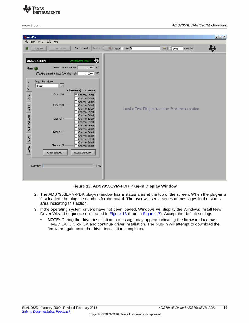
Figure 12. ADS7953EVM-PDK Plug-In Display Window
2. The ADS7953EVM-PDK plug-in window has a status area at the top of the screen. When the plug-in isfirst loaded, the plug-in searches for the board. The user will see a series of messages in the statusarea indicating this action.
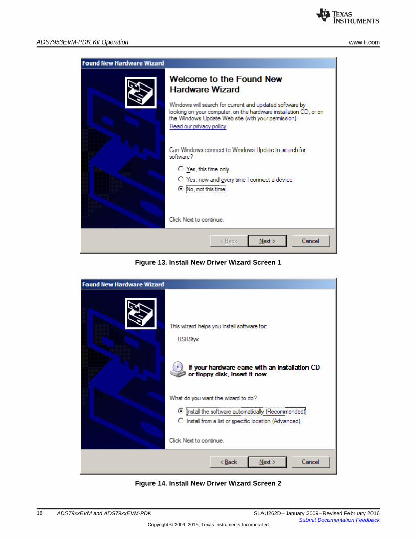
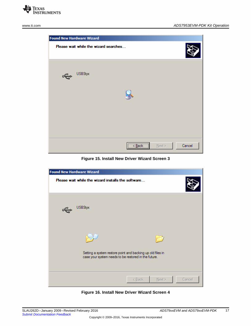
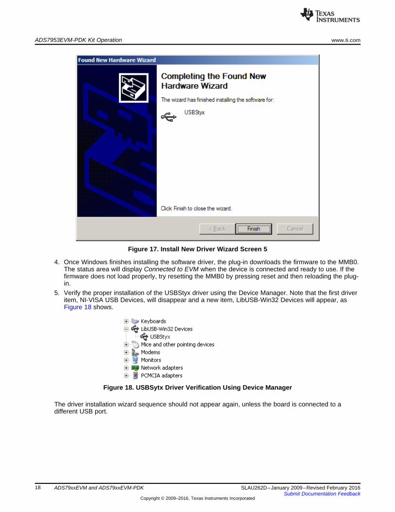
3. If the operating system drivers have not been loaded, Windows will display the Windows Install NewDriver Wizard sequence (illustrated in Figure 13 through Figure 17). Accept the default settings.• NOTE: During the driver installation, a message may appear indicating the firmware load has
TIMED OUT. Click OK and continue driver installation. The plug-in will attempt to download thefirmware again once the driver installation completes.
ADS7953EVM-PDK Kit Operation www.ti.com
16 SLAU262D–January 2009–Revised February 2016Submit Documentation Feedback
Copyright © 2009–2016, Texas Instruments Incorporated
ADS79xxEVM and ADS79xxEVM-PDK
Figure 13. Install New Driver Wizard Screen 1
Figure 14. Install New Driver Wizard Screen 2
www.ti.com ADS7953EVM-PDK Kit Operation
17SLAU262D–January 2009–Revised February 2016Submit Documentation Feedback
Copyright © 2009–2016, Texas Instruments Incorporated
ADS79xxEVM and ADS79xxEVM-PDK
Figure 15. Install New Driver Wizard Screen 3
Figure 16. Install New Driver Wizard Screen 4
ADS7953EVM-PDK Kit Operation www.ti.com
18 SLAU262D–January 2009–Revised February 2016Submit Documentation Feedback
Copyright © 2009–2016, Texas Instruments Incorporated
ADS79xxEVM and ADS79xxEVM-PDK
Figure 17. Install New Driver Wizard Screen 5
4. Once Windows finishes installing the software driver, the plug-in downloads the firmware to the MMB0.The status area will display Connected to EVM when the device is connected and ready to use. If thefirmware does not load properly, try resetting the MMB0 by pressing reset and then reloading the plug-in.
5. Verify the proper installation of the USBStyx driver using the Device Manager. Note that the first driveritem, NI-VISA USB Devices, will disappear and a new item, LibUSB-Win32 Devices will appear, asFigure 18 shows.
Figure 18. USBSytx Driver Verification Using Device Manager
The driver installation wizard sequence should not appear again, unless the board is connected to adifferent USB port.

www.ti.com Evaluating Performance with the ADCPro Software
19SLAU262D–January 2009–Revised February 2016Submit Documentation Feedback
Copyright © 2009–2016, Texas Instruments Incorporated
ADS79xxEVM and ADS79xxEVM-PDK
8 Evaluating Performance with the ADCPro SoftwareThe evaluation software is based on ADCPro, a program that operates using a variety of plug-ins. (TheADS7953EVM plug-in is installed as described in the previous section.)
To use ADCPro, load an EVM plug-in and a test plug-in. To load an EVM plug-in, select it from the EVMmenu. To load a test plug-in, select it from the Test menu. To unload a plug-in, select the Unload optionfrom the corresponding menu.
Only one of each kind of plug-in can be loaded at a time. If selecting a different plugin, the previous pluginis unloaded.
8.1 Using the ADS7953EVM-PDK Plug-inThe ADS7953EVM-PDK plug-in for ADCPro provides complete control over all settings of the ADS7953. Itconsists of a tabbed interface (see Figure 19), with different functions available on different tabs. Thesecontrols are described in this section.
The user can adjust the ADS7953EVM settings when not acquiring data. During acquisition, all controlsare disabled and settings may not be changed.
When a setting is changed on the ADS7953EVM plug-in, the setting immediately updates on the board.
Settings on the ADS7953EVM correspond to settings described in the ADS7953 product data sheet; seethe ADS7953 data sheet for details.
Because the effective sampling rate of the ADS7953 depends upon settings of the Clock Freq and thenumber of channels being sampled, the Sampling Rate indicator in the upper right corner of the plug-ininterface is always visible and updates whenever a setting changes that affects the effective 'per-channel'sampling rate.
Evaluating Performance with the ADCPro Software www.ti.com
20 SLAU262D–January 2009–Revised February 2016Submit Documentation Feedback
Copyright © 2009–2016, Texas Instruments Incorporated
ADS79xxEVM and ADS79xxEVM-PDK
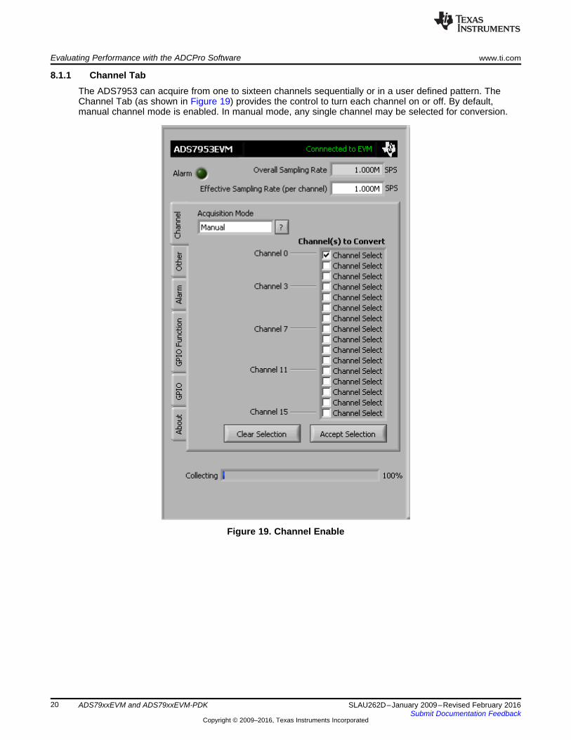
8.1.1 Channel TabThe ADS7953 can acquire from one to sixteen channels sequentially or in a user defined pattern. TheChannel Tab (as shown in Figure 19) provides the control to turn each channel on or off. By default,manual channel mode is enabled. In manual mode, any single channel may be selected for conversion.
Figure 19. Channel Enable
www.ti.com Evaluating Performance with the ADCPro Software
21SLAU262D–January 2009–Revised February 2016Submit Documentation Feedback
Copyright © 2009–2016, Texas Instruments Incorporated
ADS79xxEVM and ADS79xxEVM-PDK
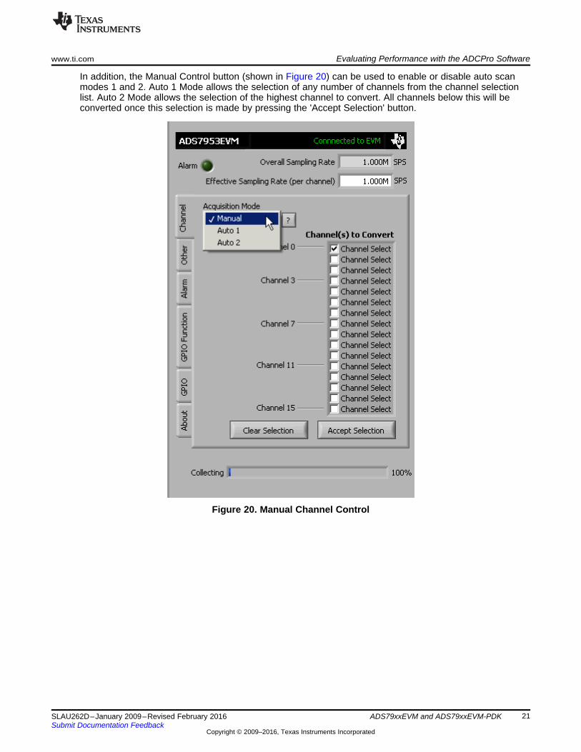
In addition, the Manual Control button (shown in Figure 20) can be used to enable or disable auto scanmodes 1 and 2. Auto 1 Mode allows the selection of any number of channels from the channel selectionlist. Auto 2 Mode allows the selection of the highest channel to convert. All channels below this will beconverted once this selection is made by pressing the 'Accept Selection' button.
Figure 20. Manual Channel Control
Evaluating Performance with the ADCPro Software www.ti.com
22 SLAU262D–January 2009–Revised February 2016Submit Documentation Feedback
Copyright © 2009–2016, Texas Instruments Incorporated
ADS79xxEVM and ADS79xxEVM-PDK
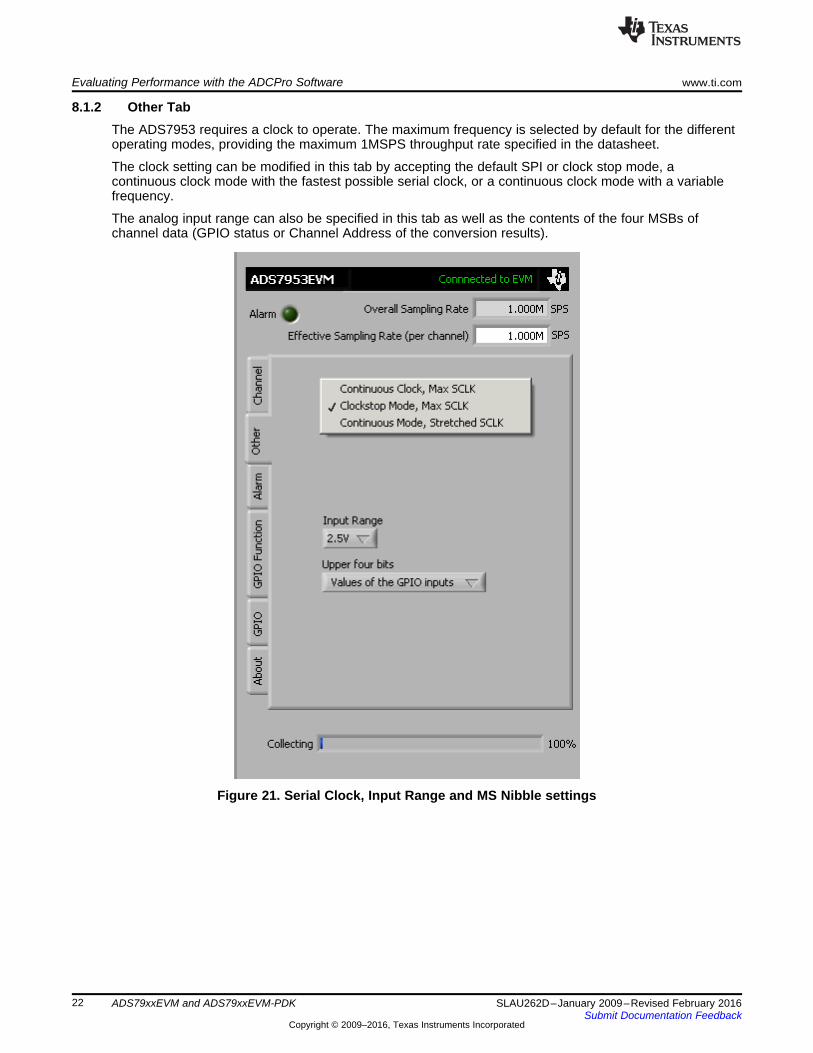
8.1.2 Other TabThe ADS7953 requires a clock to operate. The maximum frequency is selected by default for the differentoperating modes, providing the maximum 1MSPS throughput rate specified in the datasheet.
The clock setting can be modified in this tab by accepting the default SPI or clock stop mode, acontinuous clock mode with the fastest possible serial clock, or a continuous clock mode with a variablefrequency.
The analog input range can also be specified in this tab as well as the contents of the four MSBs ofchannel data (GPIO status or Channel Address of the conversion results).
Figure 21. Serial Clock, Input Range and MS Nibble settings
www.ti.com Evaluating Performance with the ADCPro Software
23SLAU262D–January 2009–Revised February 2016Submit Documentation Feedback
Copyright © 2009–2016, Texas Instruments Incorporated
ADS79xxEVM and ADS79xxEVM-PDK
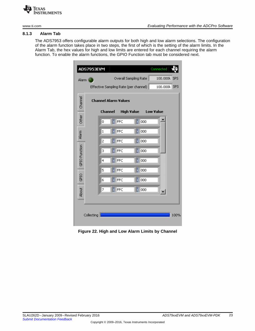
8.1.3 Alarm TabThe ADS7953 offers configurable alarm outputs for both high and low alarm selections. The configurationof the alarm function takes place in two steps, the first of which is the setting of the alarm limits. In theAlarm Tab, the hex values for high and low limits are entered for each channel requiring the alarmfunction. To enable the alarm functions, the GPIO Function tab must be considered next.
Figure 22. High and Low Alarm Limits by Channel
Evaluating Performance with the ADCPro Software www.ti.com
24 SLAU262D–January 2009–Revised February 2016Submit Documentation Feedback
Copyright © 2009–2016, Texas Instruments Incorporated
ADS79xxEVM and ADS79xxEVM-PDK
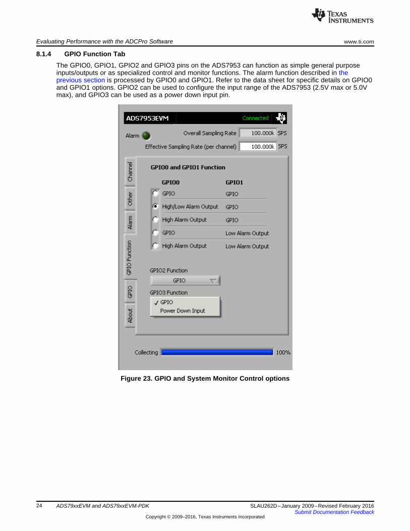
8.1.4 GPIO Function TabThe GPIO0, GPIO1, GPIO2 and GPIO3 pins on the ADS7953 can function as simple general purposeinputs/outputs or as specialized control and monitor functions. The alarm function described in theprevious section is processed by GPIO0 and GPIO1. Refer to the data sheet for specific details on GPIO0and GPIO1 options. GPIO2 can be used to configure the input range of the ADS7953 (2.5V max or 5.0Vmax), and GPIO3 can be used as a power down input pin.
Figure 23. GPIO and System Monitor Control options
www.ti.com Evaluating Performance with the ADCPro Software
25SLAU262D–January 2009–Revised February 2016Submit Documentation Feedback
Copyright © 2009–2016, Texas Instruments Incorporated
ADS79xxEVM and ADS79xxEVM-PDK
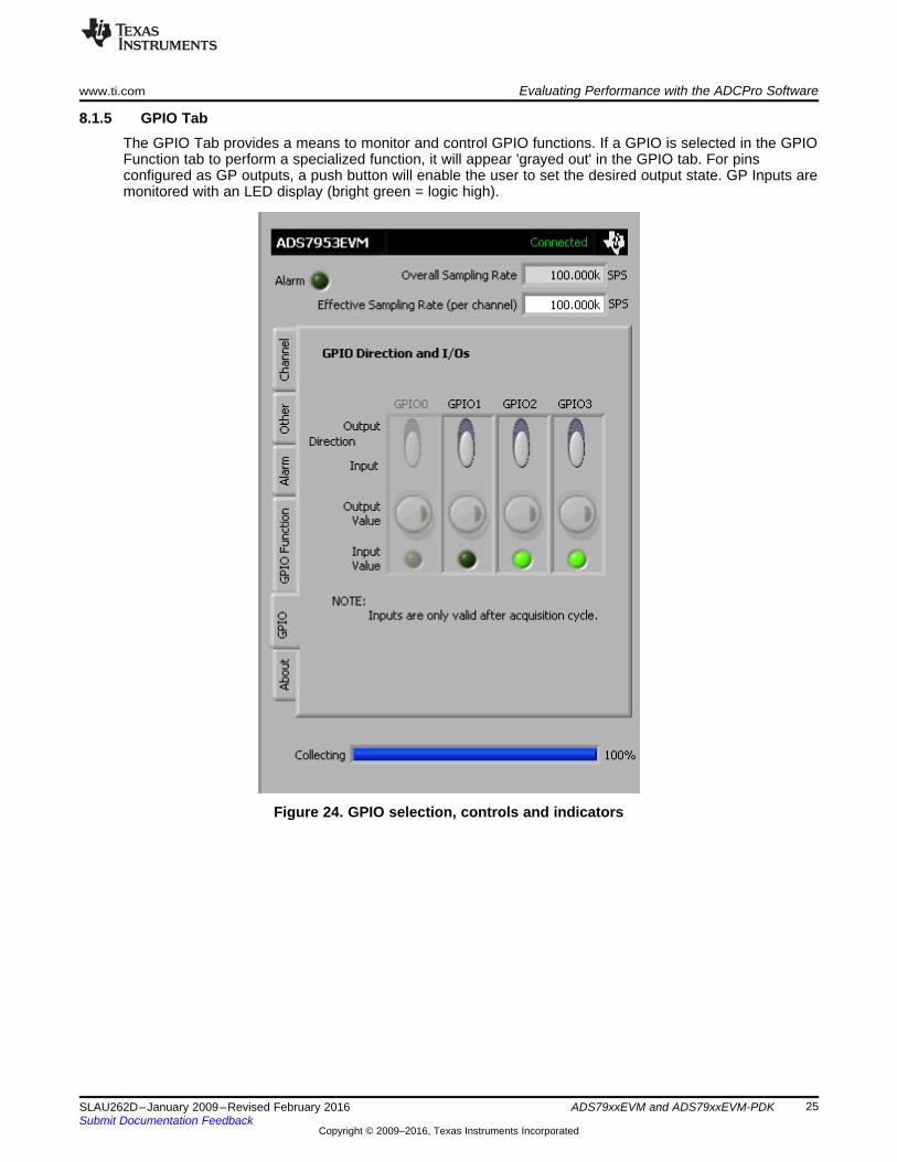
8.1.5 GPIO TabThe GPIO Tab provides a means to monitor and control GPIO functions. If a GPIO is selected in the GPIOFunction tab to perform a specialized function, it will appear 'grayed out' in the GPIO tab. For pinsconfigured as GP outputs, a push button will enable the user to set the desired output state. GP Inputs aremonitored with an LED display (bright green = logic high).
Figure 24. GPIO selection, controls and indicators
Evaluating Performance with the ADCPro Software www.ti.com
26 SLAU262D–January 2009–Revised February 2016Submit Documentation Feedback
Copyright © 2009–2016, Texas Instruments Incorporated
ADS79xxEVM and ADS79xxEVM-PDK
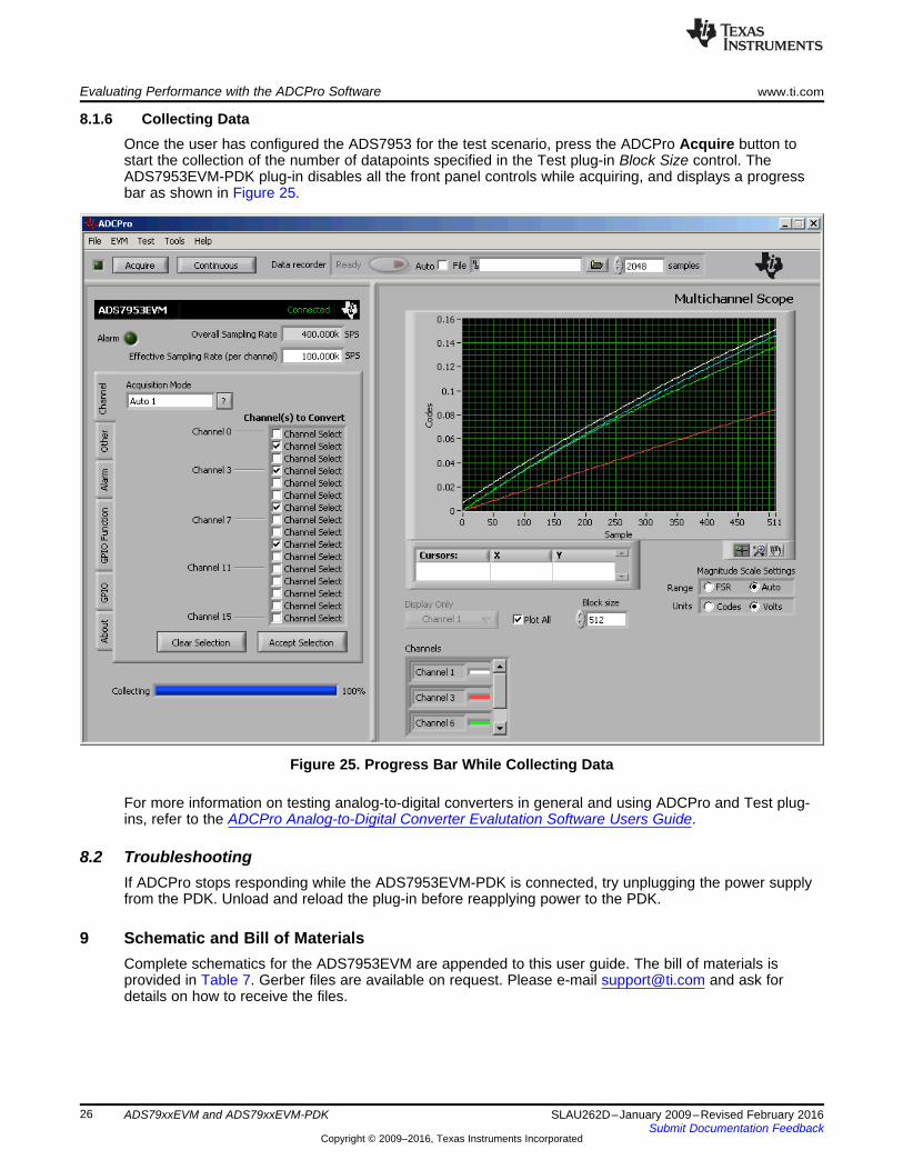
8.1.6 Collecting DataOnce the user has configured the ADS7953 for the test scenario, press the ADCPro Acquire button tostart the collection of the number of datapoints specified in the Test plug-in Block Size control. TheADS7953EVM-PDK plug-in disables all the front panel controls while acquiring, and displays a progressbar as shown in Figure 25.
Figure 25. Progress Bar While Collecting Data
For more information on testing analog-to-digital converters in general and using ADCPro and Test plug-ins, refer to the ADCPro Analog-to-Digital Converter Evalutation Software Users Guide.
8.2 TroubleshootingIf ADCPro stops responding while the ADS7953EVM-PDK is connected, try unplugging the power supplyfrom the PDK. Unload and reload the plug-in before reapplying power to the PDK.
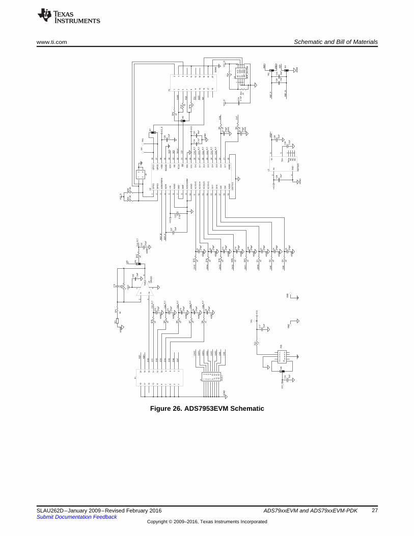
9 Schematic and Bill of MaterialsComplete schematics for the ADS7953EVM are appended to this user guide. The bill of materials isprovided in Table 7. Gerber files are available on request. Please e-mail [email protected] and ask fordetails on how to receive the files.
+V
CC
W2
R5
33
AG
ND
R13
33
AG
ND
R6
33
AG
ND
R4
33
AG
ND
R3
33
AG
ND
R2
33
AG
ND
R7
33
AG
ND
R8
33
AG
ND
R9
33
AG
ND
R10
33
AG
ND
R1
33
AG
ND
W4
CH
0
CH
1
CH
2
CH
3
CH
4
CH
5
CH
6
CH
7
CH
15
CH
14
CH
13
RE
F+
W3
RE
F-
AG
ND
-In
2
+In
3
Outp
ut
6
7 4
U1
OP
A365
R11
NI
R12
0
AG
ND
CH
0
C2
3
0.1
uF
C17
10uF
AG
ND
CH
10
CH
9
CH
8
CH
7
CH
6
AG
ND
VR
EF
+
INT
AG
ND
C12
270pF
C11
270pF
C10
270pF
C9
270pF
C8
270pF
C7
270pF
C6
270pF
C5
270pF
C4
270pF
C3
270pF
C15
NI
C2
2
270pF
C21
10uF
C25
0.1
uF
DG
ND
R15 33
SD
O
SD
I
W1
SC
LK
1357911
13
17
19
2468
10
12
14
16
18
20
15
P1
1 3 5 7 9 11
13
17
19
2 4 6 8
10
12
14
16
18
20
15
P2
C19
0.1
uF
C18
10uF
C20
1.0
uF
RE
F_M
TP
3
1 23 45 67 89 10
P3B
R16
33
R14 33
CS
*
CLK
X
FS
X
GP
IO2
1
GP
IO3
2
AG
ND
/RE
FM
3
RE
FP
4
+V
A5
AG
ND
6
MX
D7
AIN
P8
AG
ND
/AIN
M9
NC
/Ch15
11
NC
/Ch14
12
AG
ND
20
AG
ND
10
NC
/Ch13
13
NC
/Ch12
14
Ch
11
15
Ch
10
16
Ch9
17
Ch8
18
AG
ND
19
Ch7
21
Ch6
22
Ch5
23
Ch4
24
Ch3
25
Ch2
26
Ch1
27
Ch0
28
VC
C29
CS
31
SC
LK
32
VE
E30
SD
I33
SD
O34
BD
GN
D35
+V
BD
36
GP
IO0
37
GP
IO1
38
U2
AD
S79X
X
+V
CC
+V
CC
C26
10uF
Ch0_F
LT
W6
C16
0.1
uF
Ch0_F
LT
Ch1_F
LT
Ch2_F
LT
Ch3_F
LT
Ch4_F
LT
Ch5_F
LT
SD
O
SD
I
CH
12
CH
11
CH
10
CH
9
CH
8
Ch1_F
LT
Ch2_F
LT
Ch3_F
LT
Ch4_F
LT
Ch5_F
LT
R21
33
AG
ND
CH
11
C2
4
270pF
R17
33
AG
ND
CH
15
C1
270pF
R18
33
AG
ND
CH
14
C2
270pF
R19
33
AG
ND
CH
13
C1
3
270pF
R20
33
AG
ND
CH
12
C1
4
270pF
RE
F_M
TP
1
+V
CC
12
34
J2
RE
F_P
TP
2
VR
EF
+R
EF
_P
RE
F+
RE
F-
Vo
6
Trim
5
Tem
p3
GN
D4
Vin
2
NC
1
NC
7
NC
8
U3
RE
F5025
GN
DG
ND
12
34
56
78
910
11
12
13
14
15
16
J1
8X
2X
.1
R22
10
C27
10uF
+V
CC
VC
C_D
VC
C_
D
C29
1.0
uF
C28
1.0
uF
A0
1
A1
2
A2
3
GN
D4
SD
A5
SC
L6
WP
7
VC
C8
U4
MC
P_24LC
256
R24
NI
R2
333
VC
C_D
R25
47.5
KR
26
47.5
K
VC
C_D
W7
W5
C31
10uF
C30
1.0
uF
VC
C_D
www.ti.com Schematic and Bill of Materials
27SLAU262D–January 2009–Revised February 2016Submit Documentation Feedback
Copyright © 2009–2016, Texas Instruments Incorporated
ADS79xxEVM and ADS79xxEVM-PDK
Figure 26. ADS7953EVM Schematic
Schematic and Bill of Materials www.ti.com
28 SLAU262D–January 2009–Revised February 2016Submit Documentation Feedback
Copyright © 2009–2016, Texas Instruments Incorporated
Revision History
9.1 Bill of MaterialsNote: All components should be compliant with the European Union Restriction on Use of HazardousSubstances (RoHS) Directive. Some part numbers may be either leaded or RoHS. Verify that purchasedcomponents are RoHS-compliant. (For more information about TI's position on RoHS compliance, see theTI website.)
Table 7. ADS7953EVM Bill of MaterialsItem No. Qty Ref Des Description Vendor Part Number
1 1 N/A Printed Wiring Board TI
2 0 C15 Not Installed
3 0 R11 R14 R24 Not Installed
4 16 C1 - C14 C22 C24 CAP CER 270PF 50V C0G 5% 0603 TDK C1608C0G1H271J
5 4 C16 C19 C23 C25 CAP CER 0.10UF 25V X7R 10% 0603 TDK C1608X7R1E104K
6 6 C17 C18 C21 C26C27
CAP CERAMIC 10UF 6.3V X5R 0603 Panasonic ECJ-1VB0J106M
7 4 C20 C28 C29 C30 CAP CER 1.0UF 16V X7R 0603 Taiyo Yuden EMK107B7105KA-T
8 1 J1 8X2X.1 Header Samtec TMS-108-02-G-D
9 1 J2 2X2X.1 Header Samtec TMS-102-02-G-S
10 2 P1 P2 (top side) 10 Pin, Dual Row, SMT Header (20 P Samtec TSM-110-01-T-DV-P
11 2 P1B P2B (bottomside)
10 Pin, Dual Row, SMT Socket (20 P Samtec SSW-110-22-F-D-VS-K
12 1 P3 (top side) 5 Pin, Dual Row, SMT Header (10 Po Samtec TSM-105-01-T-DV-P
13 1 P3B (bottom side) 5 Pin, Dual Row, SMT Socket (10 Po Samtec SSW-105-22-F-D-VS-K
14 19 R1 - R10 R13 R15-
RES 33.0 OHM 1/10W 1% 0603 SMD Yageo RC0603FR-0733RL
15 1 R12 RES 0.0 OHM 1/10W 5% 0603 SMD Yageo RC0603JR-070RL
16 1 R22 RES 10.0 OHM 1/10W 1% 0603 SMD Yageo RC0603FR-0710RL
17 2 R25 R26 RES 47.5K OHM 1/10W 1% 0603 SMD Yageo RC0603FR-0747K5L
18 3 TP1 TP2 TP3 TEST POINT PC MINI .040D RED Keystone 5001
19 2 GND GND TEST POINT PC MULTI PURPOSE BLK Keystone 5011
20 1 U1 2.2V, 50MHz, Low-Noise, Single-Sup TI OPA365AID
21 1 U2 12/10/8-Bit, 1 MSPS, 16/12/8/4-Cha TI ADS7953/52/51/50
22 1 U3 Low-Noise, Very Low Drift, Precisi TI REF5025ID
23 1 U4 IC SERIAL EEPROM 256K 2.5V 8-SOIC Microchip 24LC256T-I/SN
24 0 W1 Not Installed Samtec TMS-102-02-G-S
25 6 W2 - W7 3 Pin , 2mm Header Samtec TMM-103-01-T-S
Revision History
Changes from C Revision (August 2011) to D Revision ................................................................................................ Page
• Replaced reference of adapter to external supply in the ADS7953EVM-PDK Power Supply section. ........................ 7• Removed reference of adapter in the ADS7953EVM-PDK Kit Operation section. .............................................. 8• Replaced reference of adapter in the Setting Up the ADS7953EVM-PDK section. ............................................. 8• Modified MMB0 Initial Setup image. ................................................................................................... 9• Replaced reference of adapter in the Connecting the Power Supply section. ................................................... 9• Replaced reference of adapter to external supply in the Connecting an External Power Supply section. .................. 10• Modified Connecting an External Power Supply image. ........................................................................... 10• Modified Laboratory Power-Supply Connection image. ............................................................................ 11
NOTE: Page numbers for previous revisions may differ from page numbers in the current version.
STANDARD TERMS AND CONDITIONS FOR EVALUATION MODULES1. Delivery: TI delivers TI evaluation boards, kits, or modules, including any accompanying demonstration software, components, or
documentation (collectively, an “EVM” or “EVMs”) to the User (“User”) in accordance with the terms and conditions set forth herein.Acceptance of the EVM is expressly subject to the following terms and conditions.1.1 EVMs are intended solely for product or software developers for use in a research and development setting to facilitate feasibility
evaluation, experimentation, or scientific analysis of TI semiconductors products. EVMs have no direct function and are notfinished products. EVMs shall not be directly or indirectly assembled as a part or subassembly in any finished product. Forclarification, any software or software tools provided with the EVM (“Software”) shall not be subject to the terms and conditionsset forth herein but rather shall be subject to the applicable terms and conditions that accompany such Software
1.2 EVMs are not intended for consumer or household use. EVMs may not be sold, sublicensed, leased, rented, loaned, assigned,or otherwise distributed for commercial purposes by Users, in whole or in part, or used in any finished product or productionsystem.
2 Limited Warranty and Related Remedies/Disclaimers:2.1 These terms and conditions do not apply to Software. The warranty, if any, for Software is covered in the applicable Software
License Agreement.2.2 TI warrants that the TI EVM will conform to TI's published specifications for ninety (90) days after the date TI delivers such EVM
to User. Notwithstanding the foregoing, TI shall not be liable for any defects that are caused by neglect, misuse or mistreatmentby an entity other than TI, including improper installation or testing, or for any EVMs that have been altered or modified in anyway by an entity other than TI. Moreover, TI shall not be liable for any defects that result from User's design, specifications orinstructions for such EVMs. Testing and other quality control techniques are used to the extent TI deems necessary or asmandated by government requirements. TI does not test all parameters of each EVM.
2.3 If any EVM fails to conform to the warranty set forth above, TI's sole liability shall be at its option to repair or replace such EVM,or credit User's account for such EVM. TI's liability under this warranty shall be limited to EVMs that are returned during thewarranty period to the address designated by TI and that are determined by TI not to conform to such warranty. If TI elects torepair or replace such EVM, TI shall have a reasonable time to repair such EVM or provide replacements. Repaired EVMs shallbe warranted for the remainder of the original warranty period. Replaced EVMs shall be warranted for a new full ninety (90) daywarranty period.
3 Regulatory Notices:3.1 United States
3.1.1 Notice applicable to EVMs not FCC-Approved:This kit is designed to allow product developers to evaluate electronic components, circuitry, or software associated with the kitto determine whether to incorporate such items in a finished product and software developers to write software applications foruse with the end product. This kit is not a finished product and when assembled may not be resold or otherwise marketed unlessall required FCC equipment authorizations are first obtained. Operation is subject to the condition that this product not causeharmful interference to licensed radio stations and that this product accept harmful interference. Unless the assembled kit isdesigned to operate under part 15, part 18 or part 95 of this chapter, the operator of the kit must operate under the authority ofan FCC license holder or must secure an experimental authorization under part 5 of this chapter.3.1.2 For EVMs annotated as FCC – FEDERAL COMMUNICATIONS COMMISSION Part 15 Compliant:
CAUTIONThis device complies with part 15 of the FCC Rules. Operation is subject to the following two conditions: (1) This device may notcause harmful interference, and (2) this device must accept any interference received, including interference that may causeundesired operation.Changes or modifications not expressly approved by the party responsible for compliance could void the user's authority tooperate the equipment.
FCC Interference Statement for Class A EVM devicesNOTE: This equipment has been tested and found to comply with the limits for a Class A digital device, pursuant to part 15 ofthe FCC Rules. These limits are designed to provide reasonable protection against harmful interference when the equipment isoperated in a commercial environment. This equipment generates, uses, and can radiate radio frequency energy and, if notinstalled and used in accordance with the instruction manual, may cause harmful interference to radio communications.Operation of this equipment in a residential area is likely to cause harmful interference in which case the user will be required tocorrect the interference at his own expense.
SPACER
SPACER
SPACER
SPACER
SPACER
SPACER
SPACER
SPACER
FCC Interference Statement for Class B EVM devicesNOTE: This equipment has been tested and found to comply with the limits for a Class B digital device, pursuant to part 15 ofthe FCC Rules. These limits are designed to provide reasonable protection against harmful interference in a residentialinstallation. This equipment generates, uses and can radiate radio frequency energy and, if not installed and used in accordancewith the instructions, may cause harmful interference to radio communications. However, there is no guarantee that interferencewill not occur in a particular installation. If this equipment does cause harmful interference to radio or television reception, whichcan be determined by turning the equipment off and on, the user is encouraged to try to correct the interference by one or moreof the following measures:
• Reorient or relocate the receiving antenna.• Increase the separation between the equipment and receiver.• Connect the equipment into an outlet on a circuit different from that to which the receiver is connected.• Consult the dealer or an experienced radio/TV technician for help.
3.2 Canada3.2.1 For EVMs issued with an Industry Canada Certificate of Conformance to RSS-210
Concerning EVMs Including Radio Transmitters:This device complies with Industry Canada license-exempt RSS standard(s). Operation is subject to the following two conditions:(1) this device may not cause interference, and (2) this device must accept any interference, including interference that maycause undesired operation of the device.
Concernant les EVMs avec appareils radio:Le présent appareil est conforme aux CNR d'Industrie Canada applicables aux appareils radio exempts de licence. L'exploitationest autorisée aux deux conditions suivantes: (1) l'appareil ne doit pas produire de brouillage, et (2) l'utilisateur de l'appareil doitaccepter tout brouillage radioélectrique subi, même si le brouillage est susceptible d'en compromettre le fonctionnement.
Concerning EVMs Including Detachable Antennas:Under Industry Canada regulations, this radio transmitter may only operate using an antenna of a type and maximum (or lesser)gain approved for the transmitter by Industry Canada. To reduce potential radio interference to other users, the antenna typeand its gain should be so chosen that the equivalent isotropically radiated power (e.i.r.p.) is not more than that necessary forsuccessful communication. This radio transmitter has been approved by Industry Canada to operate with the antenna typeslisted in the user guide with the maximum permissible gain and required antenna impedance for each antenna type indicated.Antenna types not included in this list, having a gain greater than the maximum gain indicated for that type, are strictly prohibitedfor use with this device.
Concernant les EVMs avec antennes détachablesConformément à la réglementation d'Industrie Canada, le présent émetteur radio peut fonctionner avec une antenne d'un type etd'un gain maximal (ou inférieur) approuvé pour l'émetteur par Industrie Canada. Dans le but de réduire les risques de brouillageradioélectrique à l'intention des autres utilisateurs, il faut choisir le type d'antenne et son gain de sorte que la puissance isotroperayonnée équivalente (p.i.r.e.) ne dépasse pas l'intensité nécessaire à l'établissement d'une communication satisfaisante. Leprésent émetteur radio a été approuvé par Industrie Canada pour fonctionner avec les types d'antenne énumérés dans lemanuel d’usage et ayant un gain admissible maximal et l'impédance requise pour chaque type d'antenne. Les types d'antennenon inclus dans cette liste, ou dont le gain est supérieur au gain maximal indiqué, sont strictement interdits pour l'exploitation del'émetteur
3.3 Japan3.3.1 Notice for EVMs delivered in Japan: Please see http://www.tij.co.jp/lsds/ti_ja/general/eStore/notice_01.page 日本国内に
輸入される評価用キット、ボードについては、次のところをご覧ください。http://www.tij.co.jp/lsds/ti_ja/general/eStore/notice_01.page
3.3.2 Notice for Users of EVMs Considered “Radio Frequency Products” in Japan: EVMs entering Japan may not be certifiedby TI as conforming to Technical Regulations of Radio Law of Japan.
If User uses EVMs in Japan, not certified to Technical Regulations of Radio Law of Japan, User is required by Radio Law ofJapan to follow the instructions below with respect to EVMs:1. Use EVMs in a shielded room or any other test facility as defined in the notification #173 issued by Ministry of Internal
Affairs and Communications on March 28, 2006, based on Sub-section 1.1 of Article 6 of the Ministry’s Rule forEnforcement of Radio Law of Japan,
2. Use EVMs only after User obtains the license of Test Radio Station as provided in Radio Law of Japan with respect toEVMs, or
3. Use of EVMs only after User obtains the Technical Regulations Conformity Certification as provided in Radio Law of Japanwith respect to EVMs. Also, do not transfer EVMs, unless User gives the same notice above to the transferee. Please notethat if User does not follow the instructions above, User will be subject to penalties of Radio Law of Japan.
SPACER
SPACER
SPACER
SPACER
SPACER
【無線電波を送信する製品の開発キットをお使いになる際の注意事項】 開発キットの中には技術基準適合証明を受けていないものがあります。 技術適合証明を受けていないもののご使用に際しては、電波法遵守のため、以下のいずれかの措置を取っていただく必要がありますのでご注意ください。1. 電波法施行規則第6条第1項第1号に基づく平成18年3月28日総務省告示第173号で定められた電波暗室等の試験設備でご使用
いただく。2. 実験局の免許を取得後ご使用いただく。3. 技術基準適合証明を取得後ご使用いただく。
なお、本製品は、上記の「ご使用にあたっての注意」を譲渡先、移転先に通知しない限り、譲渡、移転できないものとします。上記を遵守頂けない場合は、電波法の罰則が適用される可能性があることをご留意ください。 日本テキサス・イ
ンスツルメンツ株式会社東京都新宿区西新宿6丁目24番1号西新宿三井ビル
3.3.3 Notice for EVMs for Power Line Communication: Please see http://www.tij.co.jp/lsds/ti_ja/general/eStore/notice_02.page電力線搬送波通信についての開発キットをお使いになる際の注意事項については、次のところをご覧ください。http://www.tij.co.jp/lsds/ti_ja/general/eStore/notice_02.page
SPACER4 EVM Use Restrictions and Warnings:
4.1 EVMS ARE NOT FOR USE IN FUNCTIONAL SAFETY AND/OR SAFETY CRITICAL EVALUATIONS, INCLUDING BUT NOTLIMITED TO EVALUATIONS OF LIFE SUPPORT APPLICATIONS.
4.2 User must read and apply the user guide and other available documentation provided by TI regarding the EVM prior to handlingor using the EVM, including without limitation any warning or restriction notices. The notices contain important safety informationrelated to, for example, temperatures and voltages.
4.3 Safety-Related Warnings and Restrictions:4.3.1 User shall operate the EVM within TI’s recommended specifications and environmental considerations stated in the user
guide, other available documentation provided by TI, and any other applicable requirements and employ reasonable andcustomary safeguards. Exceeding the specified performance ratings and specifications (including but not limited to inputand output voltage, current, power, and environmental ranges) for the EVM may cause personal injury or death, orproperty damage. If there are questions concerning performance ratings and specifications, User should contact a TIfield representative prior to connecting interface electronics including input power and intended loads. Any loads appliedoutside of the specified output range may also result in unintended and/or inaccurate operation and/or possiblepermanent damage to the EVM and/or interface electronics. Please consult the EVM user guide prior to connecting anyload to the EVM output. If there is uncertainty as to the load specification, please contact a TI field representative.During normal operation, even with the inputs and outputs kept within the specified allowable ranges, some circuitcomponents may have elevated case temperatures. These components include but are not limited to linear regulators,switching transistors, pass transistors, current sense resistors, and heat sinks, which can be identified using theinformation in the associated documentation. When working with the EVM, please be aware that the EVM may becomevery warm.
4.3.2 EVMs are intended solely for use by technically qualified, professional electronics experts who are familiar with thedangers and application risks associated with handling electrical mechanical components, systems, and subsystems.User assumes all responsibility and liability for proper and safe handling and use of the EVM by User or its employees,affiliates, contractors or designees. User assumes all responsibility and liability to ensure that any interfaces (electronicand/or mechanical) between the EVM and any human body are designed with suitable isolation and means to safelylimit accessible leakage currents to minimize the risk of electrical shock hazard. User assumes all responsibility andliability for any improper or unsafe handling or use of the EVM by User or its employees, affiliates, contractors ordesignees.
4.4 User assumes all responsibility and liability to determine whether the EVM is subject to any applicable international, federal,state, or local laws and regulations related to User’s handling and use of the EVM and, if applicable, User assumes allresponsibility and liability for compliance in all respects with such laws and regulations. User assumes all responsibility andliability for proper disposal and recycling of the EVM consistent with all applicable international, federal, state, and localrequirements.
5. Accuracy of Information: To the extent TI provides information on the availability and function of EVMs, TI attempts to be as accurateas possible. However, TI does not warrant the accuracy of EVM descriptions, EVM availability or other information on its websites asaccurate, complete, reliable, current, or error-free.
SPACER
SPACER
SPACER
SPACER
SPACER
SPACER
SPACER6. Disclaimers:
6.1 EXCEPT AS SET FORTH ABOVE, EVMS AND ANY WRITTEN DESIGN MATERIALS PROVIDED WITH THE EVM (AND THEDESIGN OF THE EVM ITSELF) ARE PROVIDED "AS IS" AND "WITH ALL FAULTS." TI DISCLAIMS ALL OTHERWARRANTIES, EXPRESS OR IMPLIED, REGARDING SUCH ITEMS, INCLUDING BUT NOT LIMITED TO ANY IMPLIEDWARRANTIES OF MERCHANTABILITY OR FITNESS FOR A PARTICULAR PURPOSE OR NON-INFRINGEMENT OF ANYTHIRD PARTY PATENTS, COPYRIGHTS, TRADE SECRETS OR OTHER INTELLECTUAL PROPERTY RIGHTS.
6.2 EXCEPT FOR THE LIMITED RIGHT TO USE THE EVM SET FORTH HEREIN, NOTHING IN THESE TERMS ANDCONDITIONS SHALL BE CONSTRUED AS GRANTING OR CONFERRING ANY RIGHTS BY LICENSE, PATENT, OR ANYOTHER INDUSTRIAL OR INTELLECTUAL PROPERTY RIGHT OF TI, ITS SUPPLIERS/LICENSORS OR ANY OTHER THIRDPARTY, TO USE THE EVM IN ANY FINISHED END-USER OR READY-TO-USE FINAL PRODUCT, OR FOR ANYINVENTION, DISCOVERY OR IMPROVEMENT MADE, CONCEIVED OR ACQUIRED PRIOR TO OR AFTER DELIVERY OFTHE EVM.
7. USER'S INDEMNITY OBLIGATIONS AND REPRESENTATIONS. USER WILL DEFEND, INDEMNIFY AND HOLD TI, ITSLICENSORS AND THEIR REPRESENTATIVES HARMLESS FROM AND AGAINST ANY AND ALL CLAIMS, DAMAGES, LOSSES,EXPENSES, COSTS AND LIABILITIES (COLLECTIVELY, "CLAIMS") ARISING OUT OF OR IN CONNECTION WITH ANYHANDLING OR USE OF THE EVM THAT IS NOT IN ACCORDANCE WITH THESE TERMS AND CONDITIONS. THIS OBLIGATIONSHALL APPLY WHETHER CLAIMS ARISE UNDER STATUTE, REGULATION, OR THE LAW OF TORT, CONTRACT OR ANYOTHER LEGAL THEORY, AND EVEN IF THE EVM FAILS TO PERFORM AS DESCRIBED OR EXPECTED.
8. Limitations on Damages and Liability:8.1 General Limitations. IN NO EVENT SHALL TI BE LIABLE FOR ANY SPECIAL, COLLATERAL, INDIRECT, PUNITIVE,
INCIDENTAL, CONSEQUENTIAL, OR EXEMPLARY DAMAGES IN CONNECTION WITH OR ARISING OUT OF THESETERMS ANDCONDITIONS OR THE USE OF THE EVMS PROVIDED HEREUNDER, REGARDLESS OF WHETHER TI HASBEEN ADVISED OF THE POSSIBILITY OF SUCH DAMAGES. EXCLUDED DAMAGES INCLUDE, BUT ARE NOT LIMITEDTO, COST OF REMOVAL OR REINSTALLATION, ANCILLARY COSTS TO THE PROCUREMENT OF SUBSTITUTE GOODSOR SERVICES, RETESTING, OUTSIDE COMPUTER TIME, LABOR COSTS, LOSS OF GOODWILL, LOSS OF PROFITS,LOSS OF SAVINGS, LOSS OF USE, LOSS OF DATA, OR BUSINESS INTERRUPTION. NO CLAIM, SUIT OR ACTION SHALLBE BROUGHT AGAINST TI MORE THAN ONE YEAR AFTER THE RELATED CAUSE OF ACTION HAS OCCURRED.
8.2 Specific Limitations. IN NO EVENT SHALL TI'S AGGREGATE LIABILITY FROM ANY WARRANTY OR OTHER OBLIGATIONARISING OUT OF OR IN CONNECTION WITH THESE TERMS AND CONDITIONS, OR ANY USE OF ANY TI EVMPROVIDED HEREUNDER, EXCEED THE TOTAL AMOUNT PAID TO TI FOR THE PARTICULAR UNITS SOLD UNDERTHESE TERMS AND CONDITIONS WITH RESPECT TO WHICH LOSSES OR DAMAGES ARE CLAIMED. THE EXISTENCEOF MORE THAN ONE CLAIM AGAINST THE PARTICULAR UNITS SOLD TO USER UNDER THESE TERMS ANDCONDITIONS SHALL NOT ENLARGE OR EXTEND THIS LIMIT.
9. Return Policy. Except as otherwise provided, TI does not offer any refunds, returns, or exchanges. Furthermore, no return of EVM(s)will be accepted if the package has been opened and no return of the EVM(s) will be accepted if they are damaged or otherwise not ina resalable condition. If User feels it has been incorrectly charged for the EVM(s) it ordered or that delivery violates the applicableorder, User should contact TI. All refunds will be made in full within thirty (30) working days from the return of the components(s),excluding any postage or packaging costs.
10. Governing Law: These terms and conditions shall be governed by and interpreted in accordance with the laws of the State of Texas,without reference to conflict-of-laws principles. User agrees that non-exclusive jurisdiction for any dispute arising out of or relating tothese terms and conditions lies within courts located in the State of Texas and consents to venue in Dallas County, Texas.Notwithstanding the foregoing, any judgment may be enforced in any United States or foreign court, and TI may seek injunctive reliefin any United States or foreign court.
Mailing Address: Texas Instruments, Post Office Box 655303, Dallas, Texas 75265Copyright © 2015, Texas Instruments Incorporated
spacer

IMPORTANT NOTICE
Texas Instruments Incorporated and its subsidiaries (TI) reserve the right to make corrections, enhancements, improvements and otherchanges to its semiconductor products and services per JESD46, latest issue, and to discontinue any product or service per JESD48, latestissue. Buyers should obtain the latest relevant information before placing orders and should verify that such information is current andcomplete. All semiconductor products (also referred to herein as “components”) are sold subject to TI’s terms and conditions of salesupplied at the time of order acknowledgment.TI warrants performance of its components to the specifications applicable at the time of sale, in accordance with the warranty in TI’s termsand conditions of sale of semiconductor products. Testing and other quality control techniques are used to the extent TI deems necessaryto support this warranty. Except where mandated by applicable law, testing of all parameters of each component is not necessarilyperformed.TI assumes no liability for applications assistance or the design of Buyers’ products. Buyers are responsible for their products andapplications using TI components. To minimize the risks associated with Buyers’ products and applications, Buyers should provideadequate design and operating safeguards.TI does not warrant or represent that any license, either express or implied, is granted under any patent right, copyright, mask work right, orother intellectual property right relating to any combination, machine, or process in which TI components or services are used. Informationpublished by TI regarding third-party products or services does not constitute a license to use such products or services or a warranty orendorsement thereof. Use of such information may require a license from a third party under the patents or other intellectual property of thethird party, or a license from TI under the patents or other intellectual property of TI.Reproduction of significant portions of TI information in TI data books or data sheets is permissible only if reproduction is without alterationand is accompanied by all associated warranties, conditions, limitations, and notices. TI is not responsible or liable for such altereddocumentation. Information of third parties may be subject to additional restrictions.Resale of TI components or services with statements different from or beyond the parameters stated by TI for that component or servicevoids all express and any implied warranties for the associated TI component or service and is an unfair and deceptive business practice.TI is not responsible or liable for any such statements.Buyer acknowledges and agrees that it is solely responsible for compliance with all legal, regulatory and safety-related requirementsconcerning its products, and any use of TI components in its applications, notwithstanding any applications-related information or supportthat may be provided by TI. Buyer represents and agrees that it has all the necessary expertise to create and implement safeguards whichanticipate dangerous consequences of failures, monitor failures and their consequences, lessen the likelihood of failures that might causeharm and take appropriate remedial actions. Buyer will fully indemnify TI and its representatives against any damages arising out of the useof any TI components in safety-critical applications.In some cases, TI components may be promoted specifically to facilitate safety-related applications. With such components, TI’s goal is tohelp enable customers to design and create their own end-product solutions that meet applicable functional safety standards andrequirements. Nonetheless, such components are subject to these terms.No TI components are authorized for use in FDA Class III (or similar life-critical medical equipment) unless authorized officers of the partieshave executed a special agreement specifically governing such use.Only those TI components which TI has specifically designated as military grade or “enhanced plastic” are designed and intended for use inmilitary/aerospace applications or environments. Buyer acknowledges and agrees that any military or aerospace use of TI componentswhich have not been so designated is solely at the Buyer's risk, and that Buyer is solely responsible for compliance with all legal andregulatory requirements in connection with such use.TI has specifically designated certain components as meeting ISO/TS16949 requirements, mainly for automotive use. In any case of use ofnon-designated products, TI will not be responsible for any failure to meet ISO/TS16949.
Products ApplicationsAudio www.ti.com/audio Automotive and Transportation www.ti.com/automotiveAmplifiers amplifier.ti.com Communications and Telecom www.ti.com/communicationsData Converters dataconverter.ti.com Computers and Peripherals www.ti.com/computersDLP® Products www.dlp.com Consumer Electronics www.ti.com/consumer-appsDSP dsp.ti.com Energy and Lighting www.ti.com/energyClocks and Timers www.ti.com/clocks Industrial www.ti.com/industrialInterface interface.ti.com Medical www.ti.com/medicalLogic logic.ti.com Security www.ti.com/securityPower Mgmt power.ti.com Space, Avionics and Defense www.ti.com/space-avionics-defenseMicrocontrollers microcontroller.ti.com Video and Imaging www.ti.com/videoRFID www.ti-rfid.comOMAP Applications Processors www.ti.com/omap TI E2E Community e2e.ti.comWireless Connectivity www.ti.com/wirelessconnectivity
Mailing Address: Texas Instruments, Post Office Box 655303, Dallas, Texas 75265Copyright © 2016, Texas Instruments Incorporated


![Welcome [ Aswin Rao – aswins@ti.com aswins@umich.edu ]](https://img.pdfslide.us/doc/110x75/56649d6f5503460f94a51146/welcome-aswin-rao-aswinsticom-aswinsumichedu-.jpg)