Embed Size (px)
Citation preview
1 A, Low Dropout, CMOS Linear Regulator
Data Sheet ADP1706/ADP1707/ADP1708
Rev. A Document Feedback Information furnished by Analog Devices is believed to be accurate and reliable. However, no responsibility is assumed by Analog Devices for its use, nor for any infringements of patents or other rights of third parties that may result from its use. Specifications subject to change without notice. No license is granted by implication or otherwise under any patent or patent rights of Analog Devices. Trademarks and registered trademarks are the property of their respective owners.
One Technology Way, P.O. Box 9106, Norwood, MA 02062-9106, U.S.A. Tel: 781.329.4700 ©2007–2016 Analog Devices, Inc. All rights reserved. Technical Support www.analog.com
FEATURES Maximum output current: 1 A Input voltage range: 2.5 V to 5.5 V Low shutdown current: <1 µA Low dropout voltage: 345 mV at 1 A load Initial accuracy: ±1% Accuracy over line, load, and temperature: ±2.5% 16 fixed output voltage options with soft start
0.75 V to 3.3 V (ADP1706) 16 fixed output voltage options with tracking
0.75 V to 3.3 V (ADP1707) Adjustable output voltage option
0.8 V to 5.0 V (ADP1708) Stable with small 4.7 µF ceramic output capacitor Excellent load/line transient response Current limit and thermal overload protection Logic-controlled enable Available in an 8-lead, exposed paddle SOIC and
a 3 mm × 3 mm, 8-lead exposed paddle LFCSP
APPLICATIONS Notebook computers Memory components Telecommunications equipment Network equipment DSP/FPGA/microprocessor supplies Instrumentation equipment/data acquisition systems
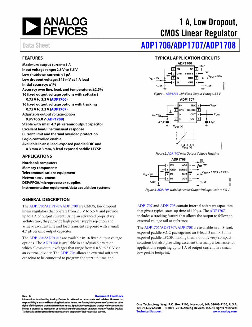
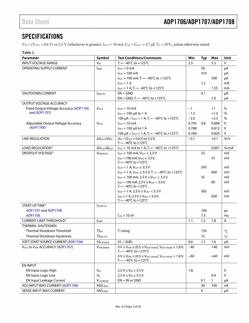
TYPICAL APPLICATION CIRCUITS
SS1
SENSE2
OUT3
OUT4
EN 8
GND 7
IN 6
IN 5
ADP170610nF
VOUT = 3.3VVIN = 5V
4.7µF4.7µF
0664
0-00
1
Figure 1. ADP1706 with Fixed Output Voltage, 3.3 V
ADP1707TRK1
SENSE2
OUT3
OUT4
EN 8
GND 7
IN 6
IN 5
VOUT
VTRK
VIN = 5V
4.7µF4.7µF
321
0 1 2 3 4 5
VOUT (V)
VTRK (V)
0664
0-00
3
Figure 2. ADP1707 with Output Voltage Tracking
ADP1708ADJ1
SENSE2
OUT3
OUT4
EN 8
GND 7
IN 6
IN 5
VOUT = 0.8V(1 + R1/R2)VIN = 5V
4.7µF4.7µF
R1
R2
0664
0-00
2
Figure 3. ADP1708 with Adjustable Output Voltage, 0.8 V to 5.0 V
GENERAL DESCRIPTION The ADP1706/ADP1707/ADP1708 are CMOS, low dropout linear regulators that operate from 2.5 V to 5.5 V and provide up to 1 A of output current. Using an advanced proprietary architecture, they provide high power supply rejection and achieve excellent line and load transient response with a small 4.7 µF ceramic output capacitor.
The ADP1706/ADP1707 are available in 16 fixed output voltage options. The ADP1708 is available in an adjustable version, which allows output voltages that range from 0.8 V to 5.0 V via an external divider. The ADP1706 allows an external soft start capacitor to be connected to program the start-up time; the
ADP1707 and ADP1708 contain internal soft start capacitors that give a typical start-up time of 100 µs. The ADP1707 includes a tracking feature that allows the output to follow an external voltage rail or reference.
The ADP1706/ADP1707/ADP1708 are available in an 8-lead, exposed paddle SOIC package and an 8-lead, 3 mm × 3 mm exposed paddle LFCSP, making them not only very compact solutions but also providing excellent thermal performance for applications requiring up to 1 A of output current in a small, low profile footprint.

ADP1706/ADP1707/ADP1708 Data Sheet
Rev. A | Page 2 of 20
TABLE OF CONTENTS Features .............................................................................................. 1 Applications ....................................................................................... 1 Typical Application Circuits ............................................................ 1 General Description ......................................................................... 1 Revision History ............................................................................... 2 Specifications ..................................................................................... 3 Absolute Maximum Ratings ............................................................ 5
Thermal Resistance ...................................................................... 5 ESD Caution .................................................................................. 5
Pin Configurations and Function Descriptions ........................... 6 Typical Performance Characteristics ............................................. 9 Theory of Operation ...................................................................... 12
Soft Start Function (ADP1706) ................................................ 12 Adjustable Output Voltage (ADP1708) ................................... 13 Track Mode (ADP1707) ............................................................ 13 Enable Feature ............................................................................ 13
Applications Information .............................................................. 14 Capacitor Selection .................................................................... 14 Voltage Tracking Applications .................................................. 14 Current Limit and Thermal Overload Protection ................. 15 Thermal Considerations ............................................................ 15 PCB Layout Considerations ...................................................... 17
Outline Dimensions ....................................................................... 18 Ordering Guide .......................................................................... 19
REVISION HISTORY 5/2016—Rev. 0 to Rev. A Changed CP-8-2 to CP-8-13 ........................................ Throughout Changes to Figure 4, Figure 5, and Table 4 ................................... 6 Moved Figure 6 and Figure 7 .......................................................... 7 Changes to Figure 6 and Figure 7 ................................................... 7 Added Table 5; Renumbered Sequentially .................................... 7 Moved Figure 8 and Figure 9 .......................................................... 8 Changes to Figure 8 and Figure 9 ................................................... 8 Added Table 6 .................................................................................... 8 Updated Outline Dimensions ....................................................... 18 Changes to Ordering Guide .......................................................... 19 6/2007—Revision 0: Initial Version
Data Sheet ADP1706/ADP1707/ADP1708
Rev. A | Page 3 of 20
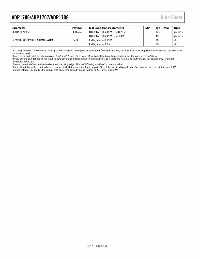
SPECIFICATIONS VIN = (VOUT + 0.6 V) or 2.5 V (whichever is greater), IOUT = 10 mA, CIN = COUT = 4.7 µF, TA = 25°C, unless otherwise noted.
Table 1. Parameter Symbol Test Conditions/Comments Min Typ Max Unit INPUT VOLTAGE RANGE VIN TJ = –40°C to +125°C 2.5 5.5 V OPERATING SUPPLY CURRENT IGND IOUT = 0 mA 50 µA IOUT = 100 mA 310 µA IOUT = 100 mA, TJ = −40°C to +125°C 390 µA IOUT = 1 A 1.2 mA IOUT = 1 A, TJ = −40°C to +125°C 1.55 mA SHUTDOWN CURRENT IGND-SD EN = GND 0.1 µA EN = GND, TJ = −40°C to +125°C 1.0 µA OUTPUT VOLTAGE ACCURACY
Fixed Output Voltage Accuracy (ADP1706 and ADP1707)
VOUT IOUT = 10 mA −1 +1 % IOUT = 100 µA to 1 A −1.5 +1.5 % 100 µA < IOUT < 1 A, TJ = −40°C to +125°C −2.5 +2.5 %
Adjustable Output Voltage Accuracy (ADP1708)1
VOUT IOUT = 10 mA 0.792 0.8 0.808 V IOUT = 100 µA to 1 A 0.788 0.812 V 100 µA < IOUT < 1 A, TJ = −40°C to +125°C 0.780 0.820 V
LINE REGULATION ∆VOUT/∆VIN VIN = (VOUT + 0.6 V) to 5.5 V, TJ = −40°C to +125°C
−0.1 +0.1 %/V
LOAD REGULATION2 ∆VOUT/∆IOUT IOUT = 10 mA to 1 A, TJ = −40°C to +125°C 0.001 %/mA DROPOUT VOLTAGE3 VDROPOUT IOUT = 100 mA, VOUT ≥ 3.3 V 33 mV IOUT = 100 mA, VOUT ≥ 3.3 V,
TJ = −40°C to +125°C 55 mV
IOUT = 1 A, VOUT ≥ 3.3 V 345 mV IOUT = 1 A, VOUT ≥ 3.3 V, TJ = −40°C to +125°C 600 mV IOUT = 100 mA, 2.5 V ≤ VOUT < 3.3 V 35 mV IOUT = 100 mA, 2.5 V ≤ VOUT < 3.3 V,
TJ = −40°C to +125°C 60 mV
IOUT = 1 A, 2.5 V ≤ VOUT < 3.3 V 365 mV IOUT = 1 A, 2.5 V ≤ VOUT < 3.3 V,
TJ = −40°C to +125°C 630 mV
START-UP TIME4 tSTART-UP ADP1707 and ADP1708 100 µs ADP1706 CSS = 10 nF 7.3 ms
CURRENT LIMIT THRESHOLD5 ILIMIT 1.1 1.5 1.8 A THERMAL SHUTDOWN
Thermal Shutdown Threshold TSSD TJ rising 150 °C Thermal Shutdown Hysteresis TSSD-HYS 15 °C
SOFT START SOURCE CURRENT (ADP1706) SSI-SOURCE SS = GND 0.6 1.1 1.6 µA VOUT to VTRK ACCURACY (ADP1707) VTRK-ERROR 0 V ≤ VTRK ≤ (0.5 × VOUT (NOM)), VOUT (NOM) ≤ 1.8 V,
TJ = −40°C to +125°C −40 +40 mV
0 V ≤ VTRK ≤ (0.5 × VOUT (NOM)), VOUT (NOM) > 1.8 V, TJ = −40°C to +125°C
−60 +60 mV
EN INPUT EN Input Logic High VIH 2.5 V ≤ VIN ≤ 5.5 V 1.8 V EN Input Logic Low VIL 2.5 V ≤ VIN ≤ 5.5 V 0.4 V EN Input Leakage Current VI-LEAKAGE EN = IN or GND 0.1 1 µA
ADJ INPUT BIAS CURRENT (ADP1708) ADJI-BIAS 30 100 nA SENSE INPUT BIAS CURRENT SNSI-BIAS 4 µA
ADP1706/ADP1707/ADP1708 Data Sheet
Rev. A | Page 4 of 20
Parameter Symbol Test Conditions/Comments Min Typ Max Unit OUTPUT NOISE OUTNOISE 10 Hz to 100 kHz, VOUT = 0.75 V 125 µV rms 10 Hz to 100 kHz, VOUT = 3.3 V 450 µV rms POWER SUPPLY REJECTION RATIO PSRR 1 kHz, VOUT = 0.75 V 70 dB 1 kHz, VOUT = 3.3 V 56 dB 1 Accuracy when OUT is connected directly to ADJ. When OUT voltage is set by external feedback resistors, absolute accuracy in adjust mode depends on the tolerances
of resistors used. 2 Based on an end-point calculation using 10 mA and 1 A loads. See Figure 11 for typical load regulation performance for loads less than 10 mA. 3 Dropout voltage is defined as the input-to-output voltage differential when the input voltage is set to the nominal output voltage. This applies only for output
voltages above 2.5 V. 4 Start-up time is defined as the time between the rising edge of EN to OUT being at 95% of its nominal value. 5 Current limit threshold is defined as the current at which the output voltage drops to 90% of the specified typical value. For example, the current limit for a 1.0 V
output voltage is defined as the current that causes the output voltage to drop to 90% of 1.0 V, or 0.9 V.

Data Sheet ADP1706/ADP1707/ADP1708
Rev. A | Page 5 of 20
ABSOLUTE MAXIMUM RATINGS Table 2. Parameter Rating IN to GND −0.3 V to +6 V OUT to GND –0.3 V to IN EN to GND –0.3 V to +6 V SS/ADJ/TRK to GND –0.3 V to +6 V SENSE to GND –0.3 V to +6 V Storage Temperature Range –65°C to +150°C Operating Junction Temperature Range –40°C to +125°C Soldering Conditions JEDEC J-STD-020
Stresses at or above those listed under Absolute Maximum Ratings may cause permanent damage to the product. This is a stress rating only; functional operation of the product at these or any other conditions above those indicated in the operational section of this specification is not implied. Operation beyond the maximum operating conditions for extended periods may affect product reliability.
THERMAL RESISTANCE θJA is specified for the worst-case conditions, that is, a device soldered in a circuit board for surface-mount packages.
Table 3. Thermal Resistance Package Type θJA Unit 8-Lead SOIC (Exposed Paddle) 58 °C/W 8-Lead 3 mm × 3 mm LFCSP (Exposed Paddle) 66 °C/W
ESD CAUTION
ADP1706/ADP1707/ADP1708 Data Sheet
Rev. A | Page 6 of 20
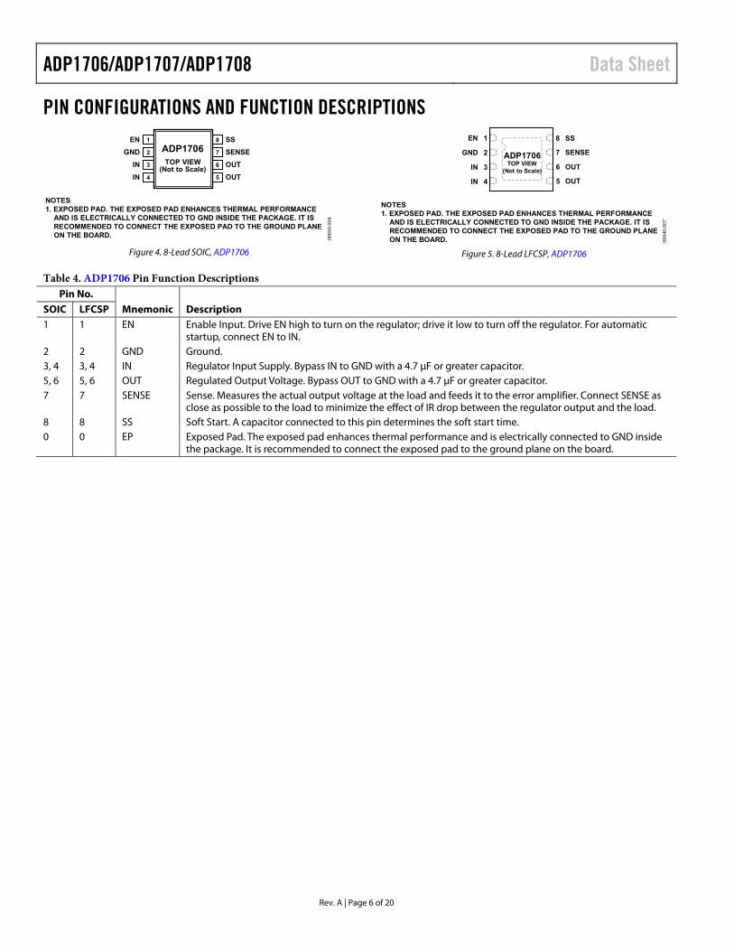
PIN CONFIGURATIONS AND FUNCTION DESCRIPTIONS EN 1
GND 2
IN 3
IN 4
SS8
SENSE7
OUT6
OUT5
ADP1706TOP VIEW
(Not to Scale)
06
640-
00
4
NOTES1. EXPOSED PAD. THE EXPOSED PAD ENHANCES THERMAL PERFORMANCE AND IS ELECTRICALLY CONNECTED TO GND INSIDE THE PACKAGE. IT IS RECOMMENDED TO CONNECT THE EXPOSED PAD TO THE GROUND PLANE ON THE BOARD.
Figure 4. 8-Lead SOIC, ADP1706
06
640
-00
7
NOTES1. EXPOSED PAD. THE EXPOSED PAD ENHANCES THERMAL PERFORMANCE AND IS ELECTRICALLY CONNECTED TO GND INSIDE THE PACKAGE. IT IS RECOMMENDED TO CONNECT THE EXPOSED PAD TO THE GROUND PLANE ON THE BOARD.
3IN
4IN
1EN
2GND
6 OUT
5 OUT
8 SS
7 SENSEADP1706TOP VIEW
(Not to Scale)
Figure 5. 8-Lead LFCSP, ADP1706
Table 4. ADP1706 Pin Function Descriptions Pin No.
Mnemonic Description SOIC LFCSP 1 1 EN Enable Input. Drive EN high to turn on the regulator; drive it low to turn off the regulator. For automatic
startup, connect EN to IN. 2 2 GND Ground. 3, 4 3, 4 IN Regulator Input Supply. Bypass IN to GND with a 4.7 μF or greater capacitor. 5, 6 5, 6 OUT Regulated Output Voltage. Bypass OUT to GND with a 4.7 μF or greater capacitor. 7 7 SENSE Sense. Measures the actual output voltage at the load and feeds it to the error amplifier. Connect SENSE as
close as possible to the load to minimize the effect of IR drop between the regulator output and the load. 8 8 SS Soft Start. A capacitor connected to this pin determines the soft start time. 0 0 EP Exposed Pad. The exposed pad enhances thermal performance and is electrically connected to GND inside
the package. It is recommended to connect the exposed pad to the ground plane on the board.
Data Sheet ADP1706/ADP1707/ADP1708
Rev. A | Page 7 of 20
EN 1
GND 2
IN 3
IN 4
TRK8
SENSE7
OUT6
OUT5
ADP1707TOP VIEW
(Not to Scale)
0664
0-0
06
NOTES1. EXPOSED PAD. THE EXPOSED PAD ENHANCES THERMAL PERFORMANCE AND IS ELECTRICALLY CONNECTED TO GND INSIDE THE PACKAGE. IT IS RECOMMENDED TO CONNECT THE EXPOSED PAD TO THE GROUND PLANE ON THE BOARD. 0
664
0-0
09
NOTES1. EXPOSED PAD. THE EXPOSED PAD ENHANCES THERMAL PERFORMANCE AND IS ELECTRICALLY CONNECTED TO GND INSIDE THE PACKAGE. IT IS RECOMMENDED TO CONNECT THE EXPOSED PAD TO THE GROUND PLANE ON THE BOARD.
3IN
4IN
1EN
2GND
6 OUT
5 OUT
8 TRK
7 SENSEADP1707TOP VIEW
(Not to Scale)
Figure 6. 8-Lead SOIC, ADP1707 Figure 7. 8-Lead LFCSP, ADP1707
Table 5. ADP1707 Pin Function Descriptions Pin No.
Mnemonic Description SOIC LFCSP 1 1 EN Enable Input. Drive EN high to turn on the regulator; drive it low to turn off the regulator. For automatic
startup, connect EN to IN. 2 2 GND Ground. 3, 4 3, 4 IN Regulator Input Supply. Bypass IN to GND with a 4.7 μF or greater capacitor. 5, 6 5, 6 OUT Regulated Output Voltage. Bypass OUT to GND with a 4.7 μF or greater capacitor. 7 7 SENSE Sense. Measures the actual output voltage at the load and feeds it to the error amplifier. Connect SENSE as
close as possible to the load to minimize the effect of IR drop between the regulator output and the load. 8 8 TRK Track. The output follows the voltage applied at the TRK pin. See the Theory of Operation section for a more
detailed description. 0 0 EP Exposed Pad. The exposed pad enhances thermal performance and is electrically connected to GND inside
the package. It is recommended to connect the exposed pad to the ground plane on the board.
ADP1706/ADP1707/ADP1708 Data Sheet
Rev. A | Page 8 of 20
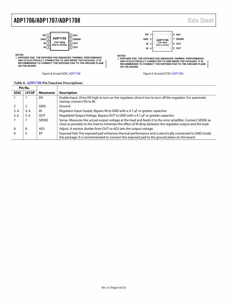
EN 1
GND 2
IN 3
IN 4
ADJ8
SENSE7
OUT6
OUT5
ADP1708TOP VIEW
(Not to Scale)
066
40-
005
NOTES1. EXPOSED PAD. THE EXPOSED PAD ENHANCES THERMAL PERFORMANCE AND IS ELECTRICALLY CONNECTED TO GND INSIDE THE PACKAGE. IT IS RECOMMENDED TO CONNECT THE EXPOSED PAD TO THE GROUND PLANE ON THE BOARD. 0
664
0-0
08
NOTES1. EXPOSED PAD. THE EXPOSED PAD ENHANCES THERMAL PERFORMANCE AND IS ELECTRICALLY CONNECTED TO GND INSIDE THE PACKAGE. IT IS RECOMMENDED TO CONNECT THE EXPOSED PAD TO THE GROUND PLANE ON THE BOARD.
3IN
4IN
1EN
2GND
6 OUT
5 OUT
8 ADJ
7 SENSEADP1708TOP VIEW
(Not to Scale)
Figure 8. 8-Lead SOIC, ADP1708 Figure 9. 8-Lead LFCSP, ADP1708
Table 6. ADP1708 Pin Function Descriptions Pin No.
Mnemonic Description SOIC LFCSP 1 1 EN Enable Input. Drive EN high to turn on the regulator; drive it low to turn off the regulator. For automatic
startup, connect EN to IN. 2 2 GND Ground. 3, 4 3, 4 IN Regulator Input Supply. Bypass IN to GND with a 4.7 μF or greater capacitor. 5, 6 5, 6 OUT Regulated Output Voltage. Bypass OUT to GND with a 4.7 μF or greater capacitor. 7 7 SENSE Sense. Measures the actual output voltage at the load and feeds it to the error amplifier. Connect SENSE as
close as possible to the load to minimize the effect of IR drop between the regulator output and the load. 8 8 ADJ Adjust. A resistor divider from OUT to ADJ sets the output voltage. 0 0 EP Exposed Pad. The exposed pad enhances thermal performance and is electrically connected to GND inside
the package. It is recommended to connect the exposed pad to the ground plane on the board.
Data Sheet ADP1706/ADP1707/ADP1708
Rev. A | Page 9 of 20
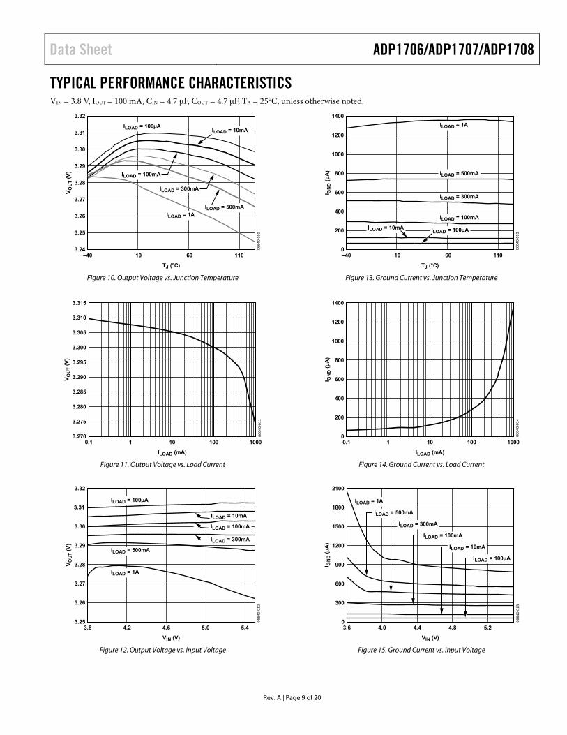
TYPICAL PERFORMANCE CHARACTERISTICS VIN = 3.8 V, IOUT = 100 mA, CIN = 4.7 μF, COUT = 4.7 μF, TA = 25°C, unless otherwise noted.
–40 10 60 110
TJ (°C)
VO
UT (
V)
3.24
3.25
3.26
3.27
3.28
3.29
3.30
3.31
3.32
ILOAD = 100µAILOAD = 10mA
ILOAD = 100mA
ILOAD = 500mAILOAD = 1A
0664
0-01
0
ILOAD = 300mA
Figure 10. Output Voltage vs. Junction Temperature
0.1 1000
ILOAD (mA)
VO
UT (
V)
1 10 1003.270
3.275
3.280
3.285
3.290
3.295
3.300
3.305
3.310
3.315
0664
0-01
1
Figure 11. Output Voltage vs. Load Current
3.8 4.2 4.6 5.0 5.4
VIN (V)
VO
UT (
V)
3.25
3.26
3.27
3.28
3.29
3.30
3.31
3.32
ILOAD = 300mA
ILOAD = 100mA
ILOAD = 10mA
ILOAD = 100µA
ILOAD = 1A
ILOAD = 500mA
0664
0-01
2
Figure 12. Output Voltage vs. Input Voltage
–40 10 60 110
TJ (°C)
I GN
D (
µA
)
0
1400
1200
1000
800
600
400
200 ILOAD = 10mA ILOAD = 100µA
ILOAD = 100mA
ILOAD = 300mA
ILOAD = 500mA
ILOAD = 1A
0664
0-01
3
Figure 13. Ground Current vs. Junction Temperature
0.1 1000
ILOAD (mA)
1 10 100
I GN
D (
µA
)
0
1400
1200
1000
800
600
400
200
0664
0-01
4
Figure 14. Ground Current vs. Load Current
2100
03.6 4.0 4.4 4.8 5.2
VIN (V)
I GN
D (
µA
)
1800
1500
1200
900
600
300
ILOAD = 100µA
ILOAD = 10mA
ILOAD = 100mA
ILOAD = 300mA
ILOAD = 500mA
ILOAD = 1A
0664
0-01
5
Figure 15. Ground Current vs. Input Voltage
ADP1706/ADP1707/ADP1708 Data Sheet
Rev. A | Page 10 of 20
400
010 1000
ILOAD (mA)
VD
RO
PO
UT (
mV
)
100
350
300
250
200
150
100
50
0664
0-01
7Figure 16. Dropout Voltage vs. Load Current
3.4
2.53.0 4.0
VIN (V)
VO
UT (
V)
3.3
3.2
3.1
3.0
2.9
2.8
2.7
2.6
3.2 3.4 3.6 3.8
ILOAD = 10mAILOAD = 100mAILOAD = 300mAILOAD = 500mAILOAD = 750mAILOAD = 1A
0664
0-01
8
Figure 17. Output Voltage vs. Input Voltage (in Dropout)
2500
03.0 4.0
VIN (V)
I GN
D (
µA
)
3.2 3.4 3.6 3.8
2000
1500
1000
500
ILOAD = 1AILOAD = 750mAILOAD = 500mAILOAD = 300mAILOAD = 100mAILOAD = 10mA
0664
0-01
9
Figure 18. Ground Current vs. Input Voltage (in Dropout)
VOUT
50m
V/D
IV
TIME (20µs/DIV)
VIN = 3.8VVOUT = 1.6VCIN = 4.7µFCOUT = 4.7µF
0664
0-02
0
LOAD SWITCHED FROM 50mA TO 950mAAND BACK TO 50mA
Figure 19. Load Transient Response, CIN = 4.7 μF, COUT = 4.7 μF
VOUT50
mV
/DIV
TIME (20μs/DIV)
VIN = 3.8VVOUT = 1.6VCIN = 22μFCOUT = 22μF
0664
0-02
1
LOAD SWITCHED FROM 50mA TO 950mAAND BACK TO 50mA
Figure 20. Load Transient Response, CIN = 22 μF, COUT = 22 μF
20m
V/D
IV2V
/DIV
TIME (100μs/DIV)
VOUT = 3.3VCIN = 4.7μFCOUT = 4.7μFILOAD = 1A
VIN STEP FROM 4V TO 5V
VOUT
0664
0-02
2
Figure 21. Line Transient Response
Data Sheet ADP1706/ADP1707/ADP1708
Rev. A | Page 11 of 20
18
00 25
CSS (nF)
RA
MP
-UP
TIM
E (
ms)
16
14
12
10
8
6
4
2
5 10 15 20
0664
0-02
3
Figure 22. Output Voltage Ramp-Up Time vs. Soft Start Capacitor Value
0
–9010 10M
FREQUENCY (Hz)
PS
RR
(d
B)
100 1k 10k 100k 1M
–10
–20
–30
–40
–50
–60
–70
–80
VRIPPLE = 50mVVIN = 5VVOUT = 3.3VCOUT = 4.7μF
ILOAD = 300mAILOAD = 200mAILOAD = 100mAILOAD = 10mAILOAD = 1mAILOAD = 100µA
0664
0-0
24
Figure 23. ADP1706 Power Supply Rejection Ratio vs. Frequency
0
–9010 10M
FREQUENCY (Hz)
PS
RR
(d
B)
100 1k 10k 100k 1M
–10
–20
–30
–40
–50
–60
–70
–80
VRIPPLE = 50mVVIN = 5VVOUT = 0.8VCOUT = 4.7μF
ILOAD = 300mAILOAD = 200mAILOAD = 100mAILOAD = 10mAILOAD = 1mAILOAD = 100µA
0664
0-0
25
Figure 24. ADP1708 Power Supply Rejection Ratio vs. Frequency
–40
–552.7 3.2 3.7 4.2 4.7
VIN (V)
PS
RR
(d
B)
–45
–50
VOUT = 2.4V
VOUT = 1.6V
VOUT = 0.8V
VRIPPLE = 50mVILOAD = 10mACOUT = 4.7μFFREQUENCY = 10kHz
0664
0-02
6
Figure 25. ADP1708 Power Supply Rejection Ratio vs. Input Voltage
–35
–550.8 4.3
VOUT (V)
PS
RR
(d
B)
–40
–45
–50
1.3 1.8 2.3 2.8 3.3 3.8
VRIPPLE = 50mVVIN = 5VILOAD = 10mACOUT = 4.7μFFREQUENCY = 10kHz
0664
0-02
7
Figure 26. ADP1708 Power Supply Rejection Ratio vs. Output Voltage
ADP1706/ADP1707/ADP1708 Data Sheet
Rev. A | Page 12 of 20
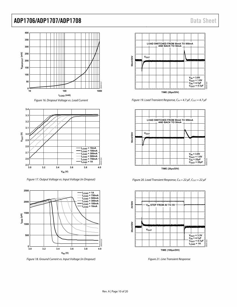
THEORY OF OPERATION The ADP1706/ADP1707/ADP1708 are low dropout linear regulators that use an advanced, proprietary architecture to provide high power supply rejection ratio (PSRR) and excellent line and load transient response with a small 4.7 μF ceramic output capacitor. All devices operate from a 2.5 V to 5.5 V input rail and provide up to 1 A of output current. Supply current in shutdown mode is typically 100 nA.
SOFTSTARTREFERENCE
CURRENT LIMITTHERMAL PROTECT
SHUTDOWN
GND
OUT
SENSE
ADJ/TRK/SS
IN
EN
066
40-0
16
Figure 27. Internal Block Diagram
Internally, the ADP1706/ADP1707/ADP1708 consist of a reference, an error amplifier, a feedback voltage divider, and a PMOS pass transistor. Output current is delivered via the PMOS pass device, which is controlled by the error amplifier. The error amplifier compares the reference voltage with the feedback voltage from the output and amplifies the difference. If the feedback voltage is lower than the reference voltage, the gate of the PMOS device is pulled lower, allowing more current to pass and increasing the output voltage. If the feedback voltage is higher than the reference voltage, the gate of the PMOS device is pulled higher, allowing less current to pass and decreasing the output voltage.
The ADP1706/ADP1707 are available in 16 fixed output voltage options between 0.75 V and 3.3 V. The ADP1706 allows for connection of an external soft start capacitor, which controls the output voltage ramp during startup. The ADP1707 features a TRK pin that allows the output voltage to follow the voltage at this pin. The ADP1708 is available in an adjustable version with an output voltage that can be set to between 0.8 V and 5.0 V by an external voltage divider. All devices are controlled by an enable pin (EN).
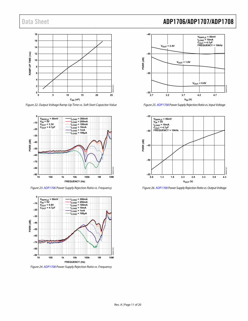
SOFT START FUNCTION (ADP1706) For applications that require a controlled startup, the ADP1706 provides a programmable soft start function. The programma-ble soft start is useful for reducing inrush current upon startup and for providing voltage sequencing. To implement a soft start, connect a small ceramic capacitor from SS to GND. Upon startup, a 1.2 μA current source charges this capacitor. The ADP1706 start-up output voltage is limited by the voltage at SS,
providing a smooth ramp-up to the nominal output voltage. The soft start time is calculated by
TSS = VREF × (CSS/ISS) (1)
where: TSS is the soft start period. VREF is the 0.8 V reference voltage. CSS is the soft start capacitance from SS to GND. ISS is the current sourced from SS (1.2 μA).
When the ADP1706 is disabled (using EN), the soft start capacitor is discharged to GND through an internal 100 Ω resistor.
TIME (2ms/DIV)
VIN = 5VVOUT = 3.3VCOUT = 4.7μFCSS = 10nFILOAD = 1A1V
/DIV
1
2V/D
IV
2
EN
OUT
0664
0-02
8
Figure 28. OUT Ramp-Up with External Soft Start Capacitor
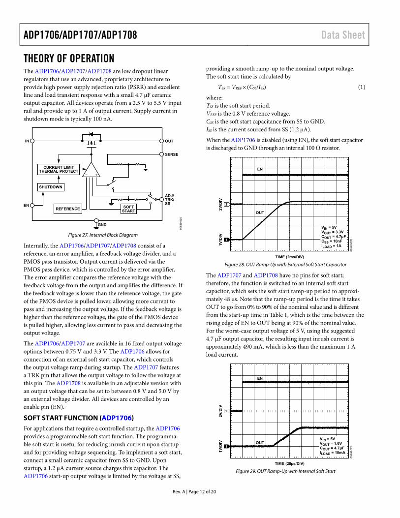
The ADP1707 and ADP1708 have no pins for soft start; therefore, the function is switched to an internal soft start capacitor, which sets the soft start ramp-up period to approxi-mately 48 μs. Note that the ramp-up period is the time it takes OUT to go from 0% to 90% of the nominal value and is different from the start-up time in Table 1, which is the time between the rising edge of EN to OUT being at 90% of the nominal value. For the worst-case output voltage of 5 V, using the suggested 4.7 μF output capacitor, the resulting input inrush current is approximately 490 mA, which is less than the maximum 1 A load current.
TIME (20µs/DIV)
VIN = 5VVOUT = 1.6VCOUT = 4.7μFILOAD = 10mA1V
/DIV
1
2V/D
IV
2
EN
OUT
0664
0-02
9
Figure 29. OUT Ramp-Up with Internal Soft Start
Data Sheet ADP1706/ADP1707/ADP1708
Rev. A | Page 13 of 20
ADJUSTABLE OUTPUT VOLTAGE (ADP1708) The ADP1708 can have its output voltage set over a 0.8 V to 5.0 V range. The output voltage is set by connecting a resistive voltage divider from OUT to ADJ. The output voltage is calculated by
VOUT = 0.8 V (1 + R1/R2) (2)
where: R1 is the resistor from OUT to ADJ. R2 is the resistor from ADJ to GND.
The maximum bias current into ADJ is 100 nA, so for less than 0.5% error due to the bias current, use values less than 60 kΩ for R2.
TRACK MODE (ADP1707) The ADP1707 includes a tracking mode feature. As shown in Figure 30, if the voltage applied at the TRK pin is less than the nominal output voltage, OUT is equal to the voltage at TRK. Otherwise, OUT regulates to its nominal output value.
4.0
00 5.0
VTRK (V)
VO
UT (
V)
3.5
3.0
2.5
2.0
1.5
1.0
0.5
0.5 1.0 1.5 2.0 2.5 3.0 3.5 4.0 4.5
0664
0-03
0
VIN = 3.8VVOUT = 3.3VILOAD = 10mA
Figure 30. ADP1707 Output Voltage vs. Tracking Voltage
For example, consider an ADP1707 with a nominal output voltage of 3.3 V. If the voltage applied to its TRK pin is greater than 3.3 V, OUT maintains a nominal output voltage of 3.3 V. If the voltage applied to TRK is reduced below 3.3 V, OUT tracks this voltage. OUT can track the TRK pin voltage from the nominal value all the way down to 0 V. A voltage divider is present from TRK to the error amplifier input with a divider ratio equal to the divider from OUT to the error amplifier, which sets the output voltage equal to the tracking voltage. Both divider ratios are set by postpackage trim, depending on the desired output voltage.
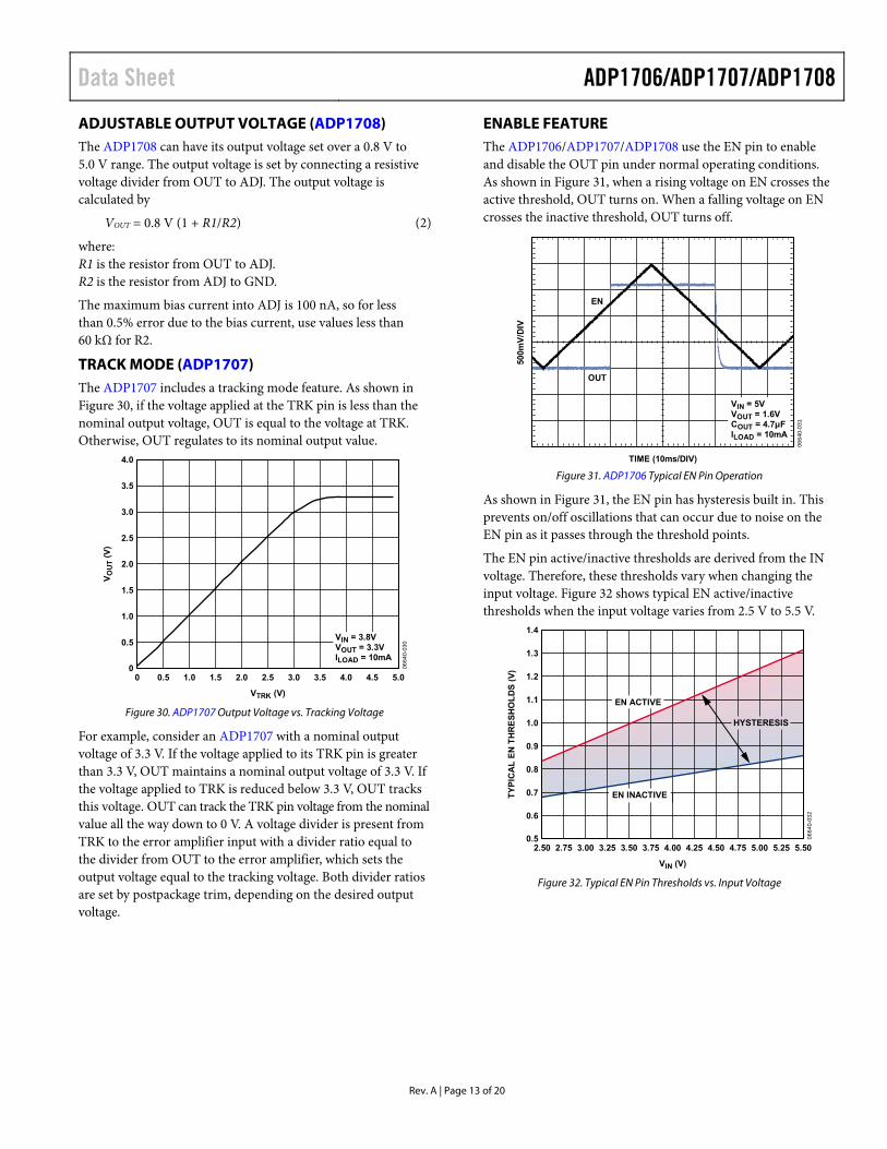
ENABLE FEATURE The ADP1706/ADP1707/ADP1708 use the EN pin to enable and disable the OUT pin under normal operating conditions. As shown in Figure 31, when a rising voltage on EN crosses the active threshold, OUT turns on. When a falling voltage on EN crosses the inactive threshold, OUT turns off.
TIME (10ms/DIV)
VIN = 5VVOUT = 1.6VCOUT = 4.7μFILOAD = 10mA
500m
V/D
IV
EN
OUT
0664
0-03
1
Figure 31. ADP1706 Typical EN Pin Operation
As shown in Figure 31, the EN pin has hysteresis built in. This prevents on/off oscillations that can occur due to noise on the EN pin as it passes through the threshold points.
The EN pin active/inactive thresholds are derived from the IN voltage. Therefore, these thresholds vary when changing the input voltage. Figure 32 shows typical EN active/inactive thresholds when the input voltage varies from 2.5 V to 5.5 V.
1.4
0.52.50 5.50
VIN (V)
TY
PIC
AL
EN
TH
RE
SH
OL
DS
(V
)
1.3
1.2
1.1
1.0
0.9
0.8
0.7
0.6
2.75 3.00 3.25 3.50 3.75 4.00 4.25 4.50 4.75 5.00 5.25
EN INACTIVE
EN ACTIVE
HYSTERESIS
0664
0-03
2
Figure 32. Typical EN Pin Thresholds vs. Input Voltage
ADP1706/ADP1707/ADP1708 Data Sheet
Rev. A | Page 14 of 20
APPLICATIONS INFORMATION CAPACITOR SELECTION Output Capacitor
The ADP1706/ADP1707/ADP1708 are designed for operation with small, space-saving ceramic capacitors, but they function with most commonly used capacitors as long as care is taken with the effective series resistance (ESR) value. The ESR of the output capacitor affects stability of the LDO control loop. A minimum of 4.7 μF capacitance with an ESR of 500 mΩ or less is recommended to ensure stability of the ADP1706/ADP1707/ADP1708. Transient response to changes in load current is also affected by output capacitance. Using a larger value of output capacitance improves the transient response of the ADP1706/ADP1707/ADP1708 to large changes in load current. Figure 33 and Figure 34 show the transient responses for output capacitance values of 4.7 μF and 22 μF, respectively.
TIME (2μs/DIV)
VIN = 3.8VVOUT = 1.6VCIN = 4.7μFCOUT = 4.7μF
50m
V/D
IV
VOUT RESPONSE TO LOAD STEPFROM 50mA TO 950mA
0664
0-03
3
Figure 33. Output Transient Response, COUT = 4.7 μF
TIME (2μs/DIV)
VIN = 3.8VVOUT = 1.6VCIN = 22μFCOUT = 22μF
50m
V/D
IV
VOUT RESPONSE TO LOAD STEPFROM 50mA TO 950mA
0664
0-03
4
Figure 34. Output Transient Response, COUT = 22 μF
Input Bypass Capacitor
Connecting a 4.7 μF capacitor from the IN pin to GND reduces the circuit sensitivity to the printed circuit board (PCB) layout, especially when long input traces, or high source impedance, is encountered. If greater than 4.7 μF of output capacitance is required, it is recommended that the input capacitor be increased to match it.
Input and Output Capacitor Properties
Any good quality ceramic capacitors can be used with the ADP1706/ADP1707/ADP1708, as long as they meet the minimum capacitance and maximum ESR requirements. Ceramic capacitors are manufactured with a variety of dielectrics, each with different behavior over temperature and applied voltage. Capacitors must have a dielectric adequate to ensure the minimum capacitance over the necessary temperature range and dc bias conditions. X5R or X7R dielectrics with a voltage rating of 6.3 V or 10 V are recommended. Y5V and Z5U dielectrics are not recommended, due to their poor temperature and dc bias characteristics.
VOLTAGE TRACKING APPLICATIONS
SS
TRK
IN
EN
IN
EN
OUT
OUT
RATIO VOLTAGE TRACKING
GND
GND
CORE RAIL
RATIOTRACKING
I/O POWER RAIL
TIME
VOUT
2.5V
1.2V
1.2V
2.5V
5V
R1
R2
ADP1706-2.5
ADP1707-1.2
0664
0-04
2
Figure 35. Voltage Tracking Feature Using the ADP1707
Figure 35 shows an application where the ADP1707 tracking feature is used. An ADP1706 powers the input/output of a microprocessor and an ADP1707 powers the core. At startup, the output of the ADP1706 ramps to 2.5 V, which is divided down via a voltage divider (R1 and R2) to a lower voltage at the TRK pin of the ADP1707. The output of the ADP1707 thus follows the TRK pin and ramps up steadily to 1.2 V. This implementation ensures that the core of the processor powers up after the input/ output.
Data Sheet ADP1706/ADP1707/ADP1708
Rev. A | Page 15 of 20
CURRENT LIMIT AND THERMAL OVERLOAD PROTECTION The ADP1706/ADP1707/ADP1708 are protected against damage due to excessive power dissipation by current and thermal overload protection circuits. The ADP1706/ ADP1707/ADP1708 are designed to reach current limit when the output load reaches 1.5 A (typical). When the output load exceeds 1.5 A, the output voltage is reduced to maintain a constant current limit.
Thermal overload protection is included, which limits the junction temperature to a maximum of 150°C (typical). Under extreme conditions (that is, high ambient temperature and power dissipation) when the junction temperature starts to rise above 150°C, the output is turned off, reducing the output current to zero. When the junction temperature drops below 135°C (typical), the output is turned on again and output current is restored to its nominal value.
Consider the case where a hard short from OUT to ground occurs. At first, the ADP1706/ADP1707/ADP1708 reach current limit so that only 1.5 A is conducted into the short. If self-heating of the junction becomes great enough to cause its temperature to rise above 150°C, thermal shutdown activates, turning off the output and reducing the output current to zero. As the junction temperature cools and drops below 135°C, the output turns on and conducts 1.5 A into the short, again causing the junction temperature to rise above 150°C. This thermal oscillation between 135°C and 150°C causes a current oscillation between 1.5 A and 0 A that continues as long as the short remains at the output.
Current and thermal limit protections are intended to protect the device against accidental overload conditions. For reliable operation, device power dissipation should be externally limited so junction temperatures do not exceed 125°C.
THERMAL CONSIDERATIONS To guarantee reliable operation, the junction temperature of the ADP1706/ADP1707/ADP1708 must not exceed 125°C. To ensure that the junction temperature stays below this maximum value, the user needs to be aware of the parameters that contrib-ute to junction temperature changes. These parameters include ambient temperature, power dissipation in the power device, and thermal resistance between the junction and ambient air (θJA). The θJA value is dependent on the package assembly compounds used and the amount of copper to which the GND pins of the package are soldered on the PCB. Table 7 shows typical θJA values of the 8-lead SOIC and 8-lead LFCSP for various PCB copper sizes.
Table 7. Typical θJA Values Copper Size (mm2) θJA (°C/W), SOIC θJA (°C/W), LFCSP 01 57.6 65.9 50 53.1 62.3 100 52.3 61.2 300 51.3 59.7 500 51.3 59.4 1 Device soldered to minimum size pin traces.
The junction temperature of the ADP1706/ADP1707/ADP1708 can be calculated by
TJ = TA + (PD × θJA) (3)
where: TA is the ambient temperature. PD is the power dissipation in the die, given by
PD = ((VIN – VOUT) × ILOAD) + (VIN × IGND) (4)
where: ILOAD is the load current. IGND is the ground current. VIN and VOUT are the input and output voltages, respectively.
Power dissipation due to ground current is quite small and can be ignored. Therefore, the junction temperature equation simplifies to the following:
TJ = TA + (((VIN – VOUT) × ILOAD) × θJA) (5)
As shown in Equation 5, for a given ambient temperature, input-to-output voltage differential, and continuous load current, a minimum copper size requirement exists for the PCB to ensure the junction temperature does not rise above 125°C. Figure 36 to Figure 41 show junction temperature calculations for different ambient temperatures, load currents, VIN to VOUT differentials, and areas of PCB copper.
ADP1706/ADP1707/ADP1708 Data Sheet
Rev. A | Page 16 of 20
140
00.5 5.0
VIN – VOUT (V)
TJ (
°C)
120
100
80
60
40
20
1.0 1.5 2.0 2.5 3.0 3.5 4.0 4.5
1mA10mA
100mA300mA
500mA750mA
1A(LOAD CURRENT)
MAX TJ (DO NOT OPERATE ABOVE THIS POINT)
0664
0-03
5
Figure 36. 500 mm2 of PCB Copper, TA = 25°C, SOIC
140
00.5 5.0
VIN – VOUT (V)
TJ (
°C)
120
100
80
60
40
20
1.0 1.5 2.0 2.5 3.0 3.5 4.0 4.5
1mA10mA
100mA300mA
500mA750mA
1A(LOAD CURRENT)
MAX TJ (DO NOT OPERATE ABOVE THIS POINT)
0664
0-03
6
Figure 37. 100 mm2 of PCB Copper, TA = 25°C, SOIC
140
00.5 5.0
VIN – VOUT (V)
TJ (
°C)
120
100
80
60
40
20
1.0 1.5 2.0 2.5 3.0 3.5 4.0 4.5
1mA10mA
100mA300mA
500mA750mA
1A(LOAD CURRENT)
MAX TJ (DO NOT OPERATE ABOVE THIS POINT)
0664
0-03
7
Figure 38. 0 mm2 of PCB Copper, TA = 25°C, SOIC
140
00.5 5.0
VIN – VOUT (V)
TJ (
°C)
120
100
80
60
40
20
1.0 1.5 2.0 2.5 3.0 3.5 4.0 4.5
1mA10mA
100mA300mA
500mA750mA
1A(LOAD CURRENT)
MAX TJ (DO NOT OPERATE ABOVE THIS POINT)
0664
0-03
8
Figure 39. 500 mm2 of PCB Copper, TA = 25°C, LFCSP
140
00.5 5.0
VIN – VOUT (V)
TJ (
°C)
120
100
80
60
40
20
1.0 1.5 2.0 2.5 3.0 3.5 4.0 4.5
1mA10mA
100mA300mA
500mA750mA
1A(LOAD CURRENT)
MAX TJ (DO NOT OPERATE ABOVE THIS POINT)
0664
0-03
9
Figure 40. 100 mm2 of PCB Copper, TA = 25°C, LFCSP
140
00.5 5.0
VIN – VOUT (V)
TJ (
°C)
120
100
80
60
40
20
1.0 1.5 2.0 2.5 3.0 3.5 4.0 4.5
1mA10mA
100mA300mA
500mA750mA
1A(LOAD CURRENT)
MAX TJ (DO NOT OPERATE ABOVE THIS POINT)
0664
0-04
0
Figure 41. 0 mm2 of PCB Copper, TA = 25°C, LFCSP
Data Sheet ADP1706/ADP1707/ADP1708
Rev. A | Page 17 of 20
PCB LAYOUT CONSIDERATIONS Heat dissipation from the package can be improved by increasing the amount of copper attached to the pins of the ADP1706/ADP1707/ADP1708. However, as can be seen from Table 7, a point of diminishing returns is eventually reached, beyond which an increase in the copper size does not yield significant heat dissipation benefits.
The ADP1706/ADP1707/ADP1708 feature an exposed pad on the bottom of both the SOIC and LFCSP packages to improve thermal performance. Because the exposed pad is electrically connected to GND inside the package, it is recommended that it also be connected to the ground plane on the PCB with a sufficient amount of copper.
Here are a few general tips when designing PCBs:
• Place the input capacitor as close as possible to the IN and GND pins.
• Place the output capacitor as close as possible to the OUT and GND pins.
• For the ADP1706, place the soft start capacitor as close as possible to the SS pin.
• Connect the load as close as possible to the OUT and SENSE pins.
Use of 0402 or 0603 size capacitors and resistors achieves the smallest possible footprint solution on boards where area is limited.
GND GND
GNDGND EN ADJ/TRK/SS
VIN VOUT
J1
R2
R1U1
C1 C2C3
ADP1706/ADP1707/ADP1708SOIC8
ANALOGDEVICES
0664
0-04
1
Figure 42. Example PCB Layout
ADP1706/ADP1707/ADP1708 Data Sheet
Rev. A | Page 18 of 20
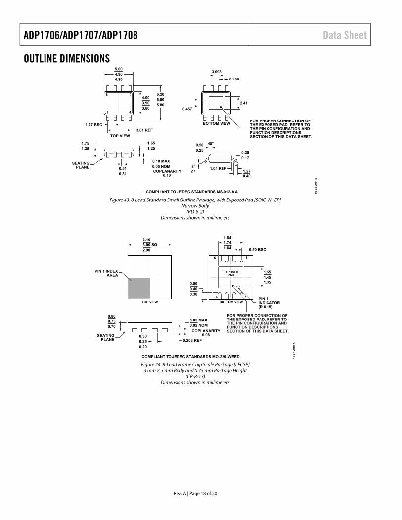
OUTLINE DIMENSIONS
COMPLIANT TO JEDEC STANDARDS MS-012-AA 06-0
3-20
11-B
1.270.40
1.751.35
2.41
0.356
0.457
4.003.903.80
6.206.005.80
5.004.904.80
0.10 MAX0.05 NOM
3.81 REF
0.250.17
8°0°
0.500.25
45°
COPLANARITY0.10
1.04 REF
8
1 4
5
1.27 BSC
SEATINGPLANE
FOR PROPER CONNECTION OFTHE EXPOSED PAD, REFER TOTHE PIN CONFIGURATION ANDFUNCTION DESCRIPTIONSSECTION OF THIS DATA SHEET.
BOTTOM VIEW
TOP VIEW
0.510.31
1.651.25
3.098
Figure 43. 8-Lead Standard Small Outline Package, with Exposed Pad [SOIC_N_EP]
Narrow Body (RD-8-2)
Dimensions shown in millimeters
TOP VIEW
8
1
5
4
0.300.250.20
BOTTOM VIEW
PIN 1 INDEXAREA
SEATINGPLANE
0.800.750.70
1.551.451.35
1.841.741.64
0.203 REF
0.05 MAX0.02 NOM
0.50 BSC
EXPOSEDPAD
3.103.00 SQ2.90
FOR PROPER CONNECTION OFTHE EXPOSED PAD, REFER TOTHE PIN CONFIGURATION ANDFUNCTION DESCRIPTIONSSECTION OF THIS DATA SHEET.COPLANARITY
0.08
0.500.400.30
COMPLIANT TOJEDEC STANDARDS MO-229-WEED 12-0
7-20
10-A
PIN 1INDICATOR(R 0.15)
Figure 44. 8-Lead Frame Chip Scale Package [LFCSP]
3 mm × 3 mm Body and 0.75 mm Package Height (CP-8-13)
Dimensions shown in millimeters

Data Sheet ADP1706/ADP1707/ADP1708
Rev. A | Page 19 of 20
ORDERING GUIDE Model1 Temperature Range Output Voltage (V) Package Description Package Option Branding ADP1706ARDZ-0.75R7 –40°C to +125°C 0.75 8-Lead SOIC_N_EP RD-8-2 ADP1706ARDZ-0.8-R7 –40°C to +125°C 0.8 8-Lead SOIC_N_EP RD-8-2 ADP1706ARDZ-0.9-R7 –40°C to +125°C 0.9 8-Lead SOIC_N_EP RD-8-2 ADP1706ARDZ-1.0-R7 –40°C to +125°C 1.0 8-Lead SOIC_N_EP RD-8-2 ADP1706ARDZ-1.1-R7 –40°C to +125°C 1.1 8-Lead SOIC_N_EP RD-8-2 ADP1706ARDZ-1.15R7 –40°C to +125°C 1.15 8-Lead SOIC_N_EP RD-8-2 ADP1706ARDZ-1.2-R7 –40°C to +125°C 1.2 8-Lead SOIC_N_EP RD-8-2 ADP1706ARDZ-1.3-R7 –40°C to +125°C 1.3 8-Lead SOIC_N_EP RD-8-2 ADP1706ARDZ-1.5-R7 –40°C to +125°C 1.5 8-Lead SOIC_N_EP RD-8-2 ADP1706ARDZ-1.8-R7 –40°C to +125°C 1.8 8-Lead SOIC_N_EP RD-8-2 ADP1706ARDZ-2.5-R7 –40°C to +125°C 2.5 8-Lead SOIC_N_EP RD-8-2 ADP1706ARDZ-3.0-R7 –40°C to +125°C 3.0 8-Lead SOIC_N_EP RD-8-2 ADP1706ARDZ-3.3-R7 –40°C to +125°C 3.3 8-Lead SOIC_N_EP RD-8-2 ADP1706ACPZ-1.0-R7 –40°C to +125°C 1.0 8-Lead LFCSP CP-8-13 L65 ADP1706ACPZ-1.05R7 –40°C to +125°C 1.05 8-Lead LFCSP CP-8-13 L67 ADP1706ACPZ-1.1-R7 –40°C to +125°C 1.1 8-Lead LFCSP CP-8-13 L66 ADP1706ACPZ-1.2-R7 –40°C to +125°C 1.2 8-Lead LFCSP CP-8-13 L6A ADP1706ACPZ-1.3-R7 –40°C to +125°C 1.3 8-Lead LFCSP CP-8-13 L6C ADP1706ACPZ-1.5-R7 –40°C to +125°C 1.5 8-Lead LFCSP CP-8-13 L6D ADP1706ACPZ-1.8-R7 –40°C to +125°C 1.8 8-Lead LFCSP CP-8-13 L6H ADP1706ACPZ-2.5-R7 –40°C to +125°C 2.5 8-Lead LFCSP CP-8-13 L6E ADP1706ACPZ-3.3-R7 –40°C to +125°C 3.3 8-Lead LFCSP CP-8-13 L6G ADP1707ARDZ-1.0-R7 –40°C to +125°C 1.0 8-Lead SOIC_N_EP RD-8-2 ADP1707ARDZ-1.1-R7 –40°C to +125°C 1.1 8-Lead SOIC_N_EP RD-8-2 ADP1707ARDZ-1.2-R7 –40°C to +125°C 1.2 8-Lead SOIC_N_EP RD-8-2 ADP1707ARDZ-1.3-R7 –40°C to +125°C 1.3 8-Lead SOIC_N_EP RD-8-2 ADP1707ARDZ-1.5-R7 –40°C to +125°C 1.5 8-Lead SOIC_N_EP RD-8-2 ADP1707ARDZ-1.8-R7 –40°C to +125°C 1.8 8-Lead SOIC_N_EP RD-8-2 ADP1707ARDZ-2.5-R7 –40°C to +125°C 2.5 8-Lead SOIC_N_EP RD-8-2 ADP1707ARDZ-3.0-R7 –40°C to +125°C 3.0 8-Lead SOIC_N_EP RD-8-2 ADP1707ARDZ-3.3-R7 –40°C to +125°C 3.3 8-Lead SOIC_N_EP RD-8-2 ADP1707ACPZ-1.3-R7 –40°C to +125°C 1.3 8-Lead LFCSP CP-8-13 L6Z ADP1707ACPZ-1.8-R7 –40°C to +125°C 1.8 8-Lead LFCSP CP-8-13 L71 ADP1707ACPZ-2.5-R7 –40°C to +125°C 2.5 8-Lead LFCSP CP-8-13 L72 ADP1707ACPZ-3.0-R7 –40°C to +125°C 3.0 8-Lead LFCSP CP-8-13 L73 ADP1707ACPZ-3.3-R7 –40°C to +125°C 3.3 8-Lead LFCSP CP-8-13 L74 ADP1708ARDZ-R7 –40°C to +125°C 0.8 to 5.0 8-Lead SOIC_N_EP RD-8-2 ADP1708ACPZ-R7 –40°C to +125°C 0.8 to 5.0 8-Lead LFCSP CP-8-13 L7P ADP1706-3.3-EVALZ 3.3 Evaluation Board ADP1707-3.3-EVALZ 3.3 Evaluation Board ADP1708-EVALZ Adjustable, but set to 1.6 V Evaluation Board 1 Z = RoHS Compliant Part.
ADP1706/ADP1707/ADP1708 Data Sheet
Rev. A | Page 20 of 20
NOTES
©2007–2016 Analog Devices, Inc. All rights reserved. Trademarks and registered trademarks are the property of their respective owners. D06640-0-5/16(A)