Embed Size (px)
Citation preview
REV. B
a
Information furnished by Analog Devices is believed to be accurate andreliable. However, no responsibility is assumed by Analog Devices for itsuse, nor for any infringements of patents or other rights of third parties thatmay result from its use. No license is granted by implication or otherwiseunder any patent or patent rights of Analog Devices.
One Technology Way, P.O. Box 9106, Norwood, MA 02062-9106, U.S.A.
Tel: 781/329-4700 www.analog.com
Fax: 781/326-8703 © Analog Devices, Inc., 2002
ADN2850*
Nonvolatile Memory, Dual 1024-Position Programmable Resistors
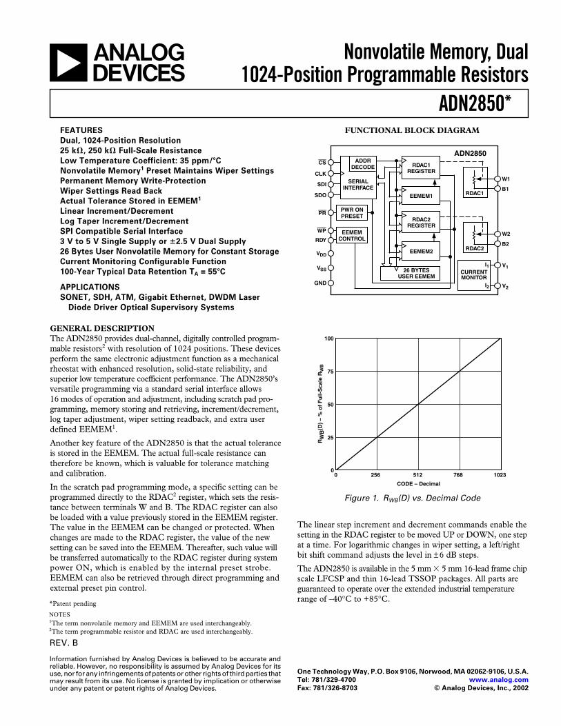
FUNCTIONAL BLOCK DIAGRAM
ADDRDECODE
ADN2850
RDAC1
SERIALINTERFACE
CS
CLK
SDI
SDO
PR
WP
RDY
VDD
VSS
GND
RDAC1REGISTER
EEMEM1
RDAC2REGISTER
EEMEM2
26 BYTESUSER EEMEM
PWR ONPRESET
EEMEMCONTROL
W1
B1
RDAC2
W2
B2
CURRENTMONITOR
I1
I2
V1
V2
CODE – Decimal
100
75
00 1023256
RW
B(D
) –
% o
f F
ull-
Sca
le R
WB
512 768
50
25
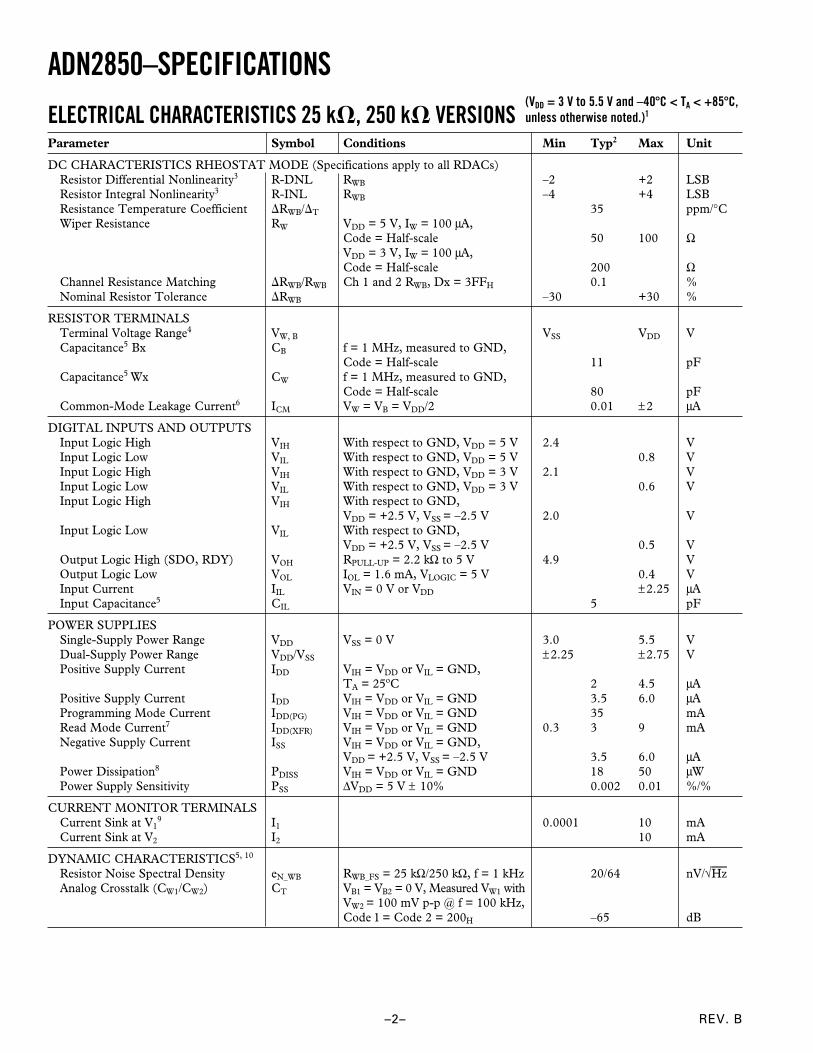
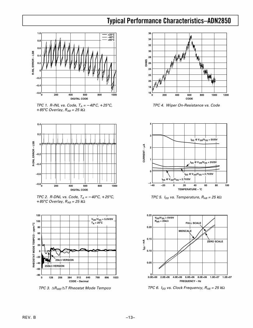
Figure 1. RWB(D) vs. Decimal Code
FEATURES
Dual, 1024-Position Resolution
25 k, 250 k Full-Scale Resistance
Low Temperature Coefficient: 35 ppm/CNonvolatile Memory1 Preset Maintains Wiper Settings
Permanent Memory Write-Protection
Wiper Settings Read Back
Actual Tolerance Stored in EEMEM1
Linear Increment/Decrement
Log Taper Increment/Decrement
SPI Compatible Serial Interface
3 V to 5 V Single Supply or 2.5 V Dual Supply
26 Bytes User Nonvolatile Memory for Constant Storage
Current Monitoring Configurable Function
100-Year Typical Data Retention TA = 55C
APPLICATIONS
SONET, SDH, ATM, Gigabit Ethernet, DWDM Laser
Diode Driver Optical Supervisory Systems
GENERAL DESCRIPTIONThe ADN2850 provides dual-channel, digitally controlled program-mable resistors2 with resolution of 1024 positions. These devicesperform the same electronic adjustment function as a mechanicalrheostat with enhanced resolution, solid-state reliability, andsuperior low temperature coefficient performance. The ADN2850’sversatile programming via a standard serial interface allows16 modes of operation and adjustment, including scratch pad pro-gramming, memory storing and retrieving, increment/decrement,log taper adjustment, wiper setting readback, and extra userdefined EEMEM1.
Another key feature of the ADN2850 is that the actual toleranceis stored in the EEMEM. The actual full-scale resistance cantherefore be known, which is valuable for tolerance matchingand calibration.
In the scratch pad programming mode, a specific setting can beprogrammed directly to the RDAC2 register, which sets the resis-tance between terminals W and B. The RDAC register can alsobe loaded with a value previously stored in the EEMEM register.The value in the EEMEM can be changed or protected. Whenchanges are made to the RDAC register, the value of the newsetting can be saved into the EEMEM. Thereafter, such value willbe transferred automatically to the RDAC register during systempower ON, which is enabled by the internal preset strobe.EEMEM can also be retrieved through direct programming andexternal preset pin control.
The linear step increment and decrement commands enable thesetting in the RDAC register to be moved UP or DOWN, one stepat a time. For logarithmic changes in wiper setting, a left/rightbit shift command adjusts the level in ±6 dB steps.
The ADN2850 is available in the 5 mm 5 mm 16-lead frame chipscale LFCSP and thin 16-lead TSSOP packages. All parts areguaranteed to operate over the extended industrial temperaturerange of –40°C to +85°C.
*Patent pending
NOTES
1The term nonvolatile memory and EEMEM are used interchangeably.2The term programmable resistor and RDAC are used interchangeably.
REV. B–2–
ADN2850–SPECIFICATIONS
ELECTRICAL CHARACTERISTICS 25 k, 250 k VERSIONSParameter Symbol Conditions Min Typ2 Max Unit
DC CHARACTERISTICS RHEOSTAT MODE (Specifications apply to all RDACs)Resistor Differential Nonlinearity3 R-DNL RWB –2 +2 LSBResistor Integral Nonlinearity3 R-INL RWB –4 +4 LSBResistance Temperature Coefficient RWB/T 35 ppm/°CWiper Resistance RW VDD = 5 V, IW = 100 µA,
Code = Half-scale 50 100 ΩVDD = 3 V, IW = 100 µA,Code = Half-scale 200 Ω
Channel Resistance Matching RWB/RWB Ch 1 and 2 RWB, Dx = 3FFH 0.1 %Nominal Resistor Tolerance RWB –30 +30 %
RESISTOR TERMINALSTerminal Voltage Range4 VW, B VSS VDD VCapacitance5 Bx CB f = 1 MHz, measured to GND,
Code = Half-scale 11 pFCapacitance5 Wx CW f = 1 MHz, measured to GND,
Code = Half-scale 80 pFCommon-Mode Leakage Current6 ICM VW = VB = VDD/2 0.01 ±2 µA
DIGITAL INPUTS AND OUTPUTSInput Logic High VIH With respect to GND, VDD = 5 V 2.4 VInput Logic Low VIL With respect to GND, VDD = 5 V 0.8 VInput Logic High VIH With respect to GND, VDD = 3 V 2.1 VInput Logic Low VIL With respect to GND, VDD = 3 V 0.6 VInput Logic High VIH With respect to GND,
VDD = +2.5 V, VSS = –2.5 V 2.0 VInput Logic Low VIL With respect to GND,
VDD = +2.5 V, VSS = –2.5 V 0.5 VOutput Logic High (SDO, RDY) VOH RPULL-UP = 2.2 kΩ to 5 V 4.9 VOutput Logic Low VOL IOL = 1.6 mA, VLOGIC = 5 V 0.4 VInput Current IIL VIN = 0 V or VDD ±2.25 µAInput Capacitance5 CIL 5 pF
POWER SUPPLIESSingle-Supply Power Range VDD VSS = 0 V 3.0 5.5 VDual-Supply Power Range VDD/VSS ±2.25 ±2.75 VPositive Supply Current IDD VIH = VDD or VIL = GND,
TA = 25oC 2 4.5 µAPositive Supply Current IDD VIH = VDD or VIL = GND 3.5 6.0 µAProgramming Mode Current IDD(PG) VIH = VDD or VIL = GND 35 mARead Mode Current7 IDD(XFR) VIH = VDD or VIL = GND 0.3 3 9 mANegative Supply Current ISS VIH = VDD or VIL = GND,
VDD = +2.5 V, VSS = –2.5 V 3.5 6.0 µAPower Dissipation8 PDISS VIH = VDD or VIL = GND 18 50 µWPower Supply Sensitivity PSS ∆VDD = 5 V ± 10% 0.002 0.01 %/%
CURRENT MONITOR TERMINALSCurrent Sink at V1
9 I1 0.0001 10 mACurrent Sink at V2 I2 10 mA
DYNAMIC CHARACTERISTICS5, 10
Resistor Noise Spectral Density eN_WB RWB_FS = 25 kΩ/250 kΩ, f = 1 kHz 20/64 nV/√HzAnalog Crosstalk (CW1/CW2) CT VB1 = VB2 = 0 V, Measured VW1 with
VW2 = 100 mV p-p @ f = 100 kHz,Code 1 = Code 2 = 200H –65 dB
(VDD = 3 V to 5.5 V and –40C < TA < +85C,unless otherwise noted.)1
REV. B
ADN2850
–3–
Parameter Symbol Conditions Min Typ2 Max Unit
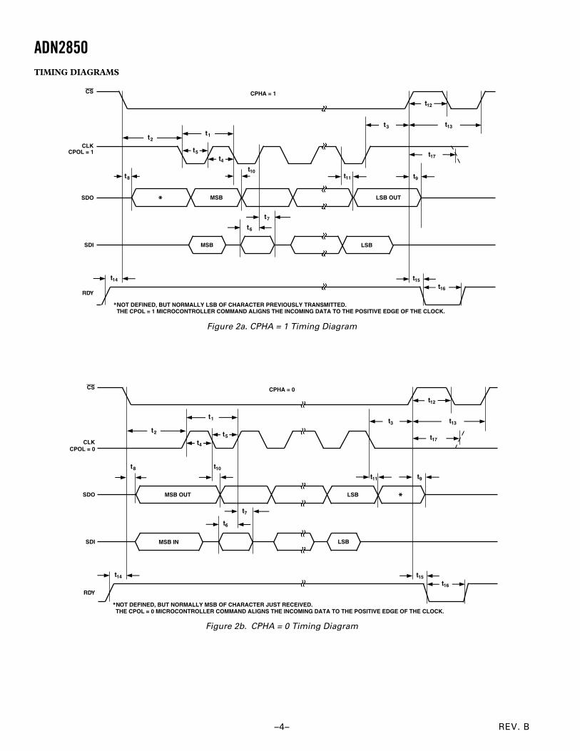
INTERFACE TIMING CHARACTERISTICS (apply to all parts)5, 11
Clock Cycle Time (tCYC) t1 20 nsCS Setup Time t2 10 nsCLK Shutdown Time to CS Rise t3 1 tCYC
Input Clock Pulsewidth t4 , t5 Clock Level High or Low 10 nsData Setup Time t6 From Positive CLK Transition 5 nsData Hold Time t7 From Positive CLK Transition 5 nsCS to SDO – SPI Line Acquire t8 40 nsCS to SDO – SPI Line Release t9 50 nsCLK to SDO Propagation Delay12 t10 RP = 2.2 kΩ, CL < 20 pF 50 nsCS High Pulsewidth13 t12 10 nsCS High to CS High13 t13 4 tCYC
RDY Rise to CS Fall t14 0 nsCS Rise to RDY Fall Time t15 0.15 0.3 msRead/Store to Nonvolatile EEMEM14 t16 Applies to Command 2H, 3H, 9H 35 msCS Rise to Clock Edge Setup t17 10 nsPreset Pulsewidth (Asynchronous) tPRW Not Shown in Timing Diagram 50 nsPreset Response Time to Wiper Setting tPRESP PR Pulsed Low to Refresh 140 µs
Wiper Positions
FLASH/EE MEMORY RELIABILITYEndurance15 100 K CyclesData Retention16 100 Years
NOTES 1 Parts can be operated at 2.7 V single supply, except from 08C to –408C, where minimum 3 V is needed. 2 Typicals represent average readings at 258C and VDD = 5 V. 3 Resistor position nonlinearity error R-INL is the deviation from an ideal value measured between the maximum resistance and the minimum resistance wiper positions.
R-DNL measures the relative step change from ideal between successive tap positions. I W ~ 50 µA for VDD = 2.7 V and IW ~ 400 µA for VDD = 5 V. 4 Resistor terminals W and B have no limitations on polarity with respect to each other. 5 Guaranteed by design and not subject to production test. 6 Common-mode leakage current is a measure of the dc leakage from any terminal B and W to a common-mode bias level of V DD/2. 7 Transfer (XFR) mode current is not continuous. Current consumed while EEMEM locations are read and transferred to the RDAC register. See TPC 9. 8 PDISS is calculated from (IDD VDD) + (ISS VSS). 9 Applies to photodiode of optical receiver.10All dynamic characteristics use VDD = +2.5 V and VSS = –2.5 V.11See timing diagram for location of measured values. All input control voltages are specified with t R = tF = 2.5 ns (10% to 90% of 3 V) and timed from a voltage level of 1.5 V.
Switching characteristics are measured using both VDD = 3 V and 5 V.12Propagation delay depends on value of VDD, RPULL_UP, and CL. See Applications section.13Valid for commands that do not activate the RDY pin.14RDY pin low only for commands 2, 3, 8, 9, 10, and PR hardware pulse: CMD_8 ~ 1 ms; CMD_9, 10 ~ 0.1 ms; CMD_2, 3 ~ 20 ms. Device operation at TA = –40°C
and VDD < 3 V extends the save time to 35 ms.15Endurance is qualified to 100,000 cycles as per JEDEC Std. 22 method A117 and measured at –40 °C, +25°C, and +85°C; typical endurance at +25°C is 700,000 cycles.16Retention lifetime equivalent at junction temperature (TJ ) = 55°C as per JEDEC Std. 22, Method A117. Retention lifetime based on an activation energy of 0.6 V will
derate with junction temperature.
Specifications subject to change without notice.The ADN2850 contains 16,000 transistors. Die size: 93 mil 103 mil, 10,197 sq mil.
REV. B–4–
ADN2850TIMING DIAGRAMS
CPOL = 1
t12
t13t3
t17
t9t11
t5
t4
t2t1
CLK
t8
* MSB LSB OUT
MSB LSB
RDY
CPHA = 1
t10
t7
t6
t14 t15t16
*NOT DEFINED, BUT NORMALLY LSB OF CHARACTER PREVIOUSLY TRANSMITTED.THE CPOL = 1 MICROCONTROLLER COMMAND ALIGNS THE INCOMING DATA TO THE POSITIVE EDGE OF THE CLOCK.
CS
SDO
SDI
Figure 2a. CPHA = 1 Timing Diagram
t12
t13t3
t17
t9
t5
t4
t2
t1
CLKCPOL = 0
t8
MSB OUT LSBSDO
MSB IN LSBSDI
RDY
CPHA = 0
t10
t7
t6
t14 t15t16
*NOT DEFINED, BUT NORMALLY MSB OF CHARACTER JUST RECEIVED. THE CPOL = 0 MICROCONTROLLER COMMAND ALIGNS THE INCOMING DATA TO THE POSITIVE EDGE OF THE CLOCK.
*
CS
t11
Figure 2b. CPHA = 0 Timing Diagram
REV. B
ADN2850
–5–
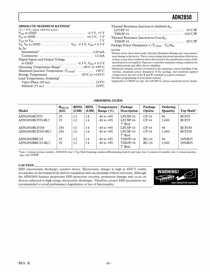
ABSOLUTE MAXIMUM RATINGS1
(TA = 25°C, unless otherwise noted.)VDD to GND . . . . . . . . . . . . . . . . . . . . . . . . . . . –0.3 V, +7 VVSS to GND . . . . . . . . . . . . . . . . . . . . . . . . . . . . +0.3 V, –7 VVDD to VSS . . . . . . . . . . . . . . . . . . . . . . . . . . . . . . . . . . . . . 7 VVB, VW to GND . . . . . . . . . . . . . . . . VSS – 0.3 V, VDD + 0.3 VIB, IW
Intermittent2 . . . . . . . . . . . . . . . . . . . . . . . . . . . . . .±20 mAContinuous . . . . . . . . . . . . . . . . . . . . . . . . . . . . . . . ±2 mA
Digital Inputs and Output Voltageto GND . . . . . . . . . . . . . . . . . . . . . . . . –0.3 V, VDD + 0.3 V
Operating Temperature Range3 . . . . . . . . . . . –40°C to +85°CMaximum Junction Temperature (TJ MAX) . . . . . . . . . 150°CStorage Temperature . . . . . . . . . . . . . . . . . . –65°C to +150°CLead Temperature, Soldering4
Vapor Phase (60 sec) . . . . . . . . . . . . . . . . . . . . . . . . . 215CInfrared (15 sec) . . . . . . . . . . . . . . . . . . . . . . . . . . . . 220C
Thermal Resistance Junction-to-Ambient θJA,
LFCSP-16 . . . . . . . . . . . . . . . . . . . . . . . . . . . . . . . 35°C/WTSSOP-16 . . . . . . . . . . . . . . . . . . . . . . . . . . . . . . 150°C/W
Thermal Resistance Junction-to-Case θJC,
TSSOP-16 . . . . . . . . . . . . . . . . . . . . . . . . . . . . . . . 28°C/WPackage Power Dissipation = (TJ MAX – TA)/θJA
NOTES1Stresses above those listed under Absolute Maximum Ratings may cause perma-nent damage to the device. This is a stress rating; functional operation of the deviceat these or any other conditions above those listed in the operational sections of thisspecification is not implied. Exposure to absolute maximum rating conditions forextended periods may affect device reliability.
2Maximum terminal current is bounded by the maximum current handling of theswitches, maximum power dissipation of the package, and maximum appliedvoltage across any two of the B and W terminals at a given resistance.
3Includes programming of nonvolatile memory.4Applicable to TSSOP-16 only. For LFCSP-16, please consult factory for details.
CAUTIONESD (electrostatic discharge) sensitive device. Electrostatic charges as high as 4000 V readilyaccumulate on the human body and test equipment and can discharge without detection. Althoughthe ADN2850 features proprietary ESD protection circuitry, permanent damage may occur ondevices subjected to high energy electrostatic discharges. Therefore, proper ESD precautions arerecommended to avoid performance degradation or loss of functionality.
WARNING!
ESD SENSITIVE DEVICE
ORDERING GUIDE
RWB_FS RDNL RINL Temperature Package Package OrderingModel (k) (LSB) (LSB) Range (°C) Description Option Quantity Top Mark*
ADN2850BCP25 25 ±2 ±4 –40 to +85 LFCSP-16 CP-16 96 BCP25ADN2850BCP25-RL7 25 ±2 ±4 –40 to +85 LFCSP-16 CP-16 1,000 BCP25
7" ReelADN2850BCP250 250 ±2 ±4 –40 to +85 LFCSP-16 CP-16 96 BCP250ADN2850BCP250-RL7 250 ±2 ±4 –40 to +85 LFCSP-16 CP-16 1,000 BCP250
7" ReelADN2850BRU25 25 ±2 ±4 –40 to +85 TSSOP-16 RU-16 96 2850B25ADN2850BRU25-RL7 25 ±2 ±4 –40 to +85 TSSOP-16 RU-16 1,000 2850B25
7" Reel
*Line 1 contains product number, ADN2850, line 2 Top Mark branding contains differentiating detail by part type, line 3 contains lot number, line 4 contains productdate code YYWW.
REV. B–6–
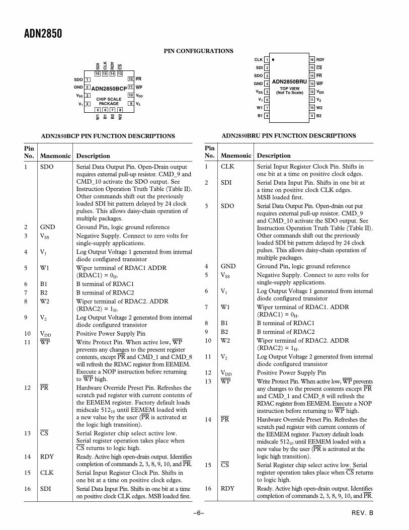
ADN2850
VSS
GND
V1 V2
PR
WP
VDD
16
CS
RD
Y
CL
K
SD
I
W2
B2
B1
W1
ADN2850BCP
CHIP SCALEPACKAGE
15 14 1312
11
10
9
8765
SDO
4
3
2
1
ADN2850BCP PIN FUNCTION DESCRIPTIONS
PinNo. Mnemonic Description
1 SDO Serial Data Output Pin. Open-Drain outputrequires external pull-up resistor. CMD_9 andCMD_10 activate the SDO output. SeeInstruction Operation Truth Table (Table II).Other commands shift out the previouslyloaded SDI bit pattern delayed by 24 clockpulses. This allows daisy-chain operation ofmultiple packages.
2 GND Ground Pin, logic ground reference3 VSS Negative Supply. Connect to zero volts for
single-supply applications.4 V1 Log Output Voltage 1 generated from internal
diode configured transistor5 W1 Wiper terminal of RDAC1 ADDR
(RDAC1) = 0H.6 B1 B terminal of RDAC17 B2 B terminal of RDAC28 W2 Wiper terminal of RDAC2. ADDR
(RDAC2) = 1H.9 V2 Log Output Voltage 2 generated from internal
diode configured transistor10 VDD Positive Power Supply Pin11 WP Write Protect Pin. When active low, WP
prevents any changes to the present registercontents, except PR and CMD_1 and CMD_8will refresh the RDAC register from EEMEM.Execute a NOP instruction before returningto WP high.
12 PR Hardware Override Preset Pin. Refreshes thescratch pad register with current contents ofthe EEMEM register. Factory default loadsmidscale 51210 until EEMEM loaded witha new value by the user (PR is activated atthe logic high transition).
13 CS Serial Register chip select active low.Serial register operation takes place whenCS returns to logic high.
14 RDY Ready. Active high open-drain output. Identifiescompletion of commands 2, 3, 8, 9, 10, and PR.
15 CLK Serial Input Register Clock Pin. Shifts inone bit at a time on positive clock edges.
16 SDI Serial Data Input Pin. Shifts in one bit at a timeon positive clock CLK edges. MSB loaded first.
TOP VIEW(Not To Scale)
1
2
3
4
5
6
7
8
SDI
SDO
GND
V1
VSS
W1
ADN2850BRU
CLK
B1
16
15
14
13
12
11
10
9
CS
PR
WP
VDD
V2
W2
B2
RDY
ADN2850BRU PIN FUNCTION DESCRIPTIONS
PinNo. Mnemonic Description
1 CLK Serial Input Register Clock Pin. Shifts inone bit at a time on positive clock edges.
2 SDI Serial Data Input Pin. Shifts in one bit ata time on positive clock CLK edges.MSB loaded first.
3 SDO Serial Data Output Pin. Open-drain out putrequires external pull-up resistor. CMD_9and CMD_10 activate the SDO output. SeeInstruction Operation Truth Table (Table II).Other commands shift out the previouslyloaded SDI bit pattern delayed by 24 clockpulses. This allows daisy-chain operation ofmultiple packages.
4 GND Ground Pin, logic ground reference5 VSS Negative Supply. Connect to zero volts for
single-supply applications.6 V1 Log Output Voltage 1 generated from internal
diode configured transistor7 W1 Wiper terminal of RDAC1. ADDR
(RDAC1) = 0H.8 B1 B terminal of RDAC19 B2 B terminal of RDAC210 W2 Wiper terminal of RDAC2. ADDR
(RDAC2) = 1H.11 V2 Log Output Voltage 2 generated from internal
diode configured transistor12 VDD Positive Power Supply Pin13 WP Write Protect Pin. When active low, WP prevents
any changes to the present contents except PRand CMD_1 and CMD_8 will refresh theRDAC register from EEMEM. Execute a NOPinstruction before returning to WP high.
14 PR Hardware Override Preset Pin. Refreshes thescratch pad register with current contents ofthe EEMEM register. Factory default loadsmidscale 51210 until EEMEM loaded with anew value by the user (PR is activated at thelogic high transition).
15 CS Serial Register chip select active low. Serialregister operation takes place when CS returnsto logic high.
16 RDY Ready. Active high open-drain output. Identifiescompletion of commands 2, 3, 8, 9, 10, and PR.
PIN CONFIGURATIONS
REV. B
ADN2850
–7–
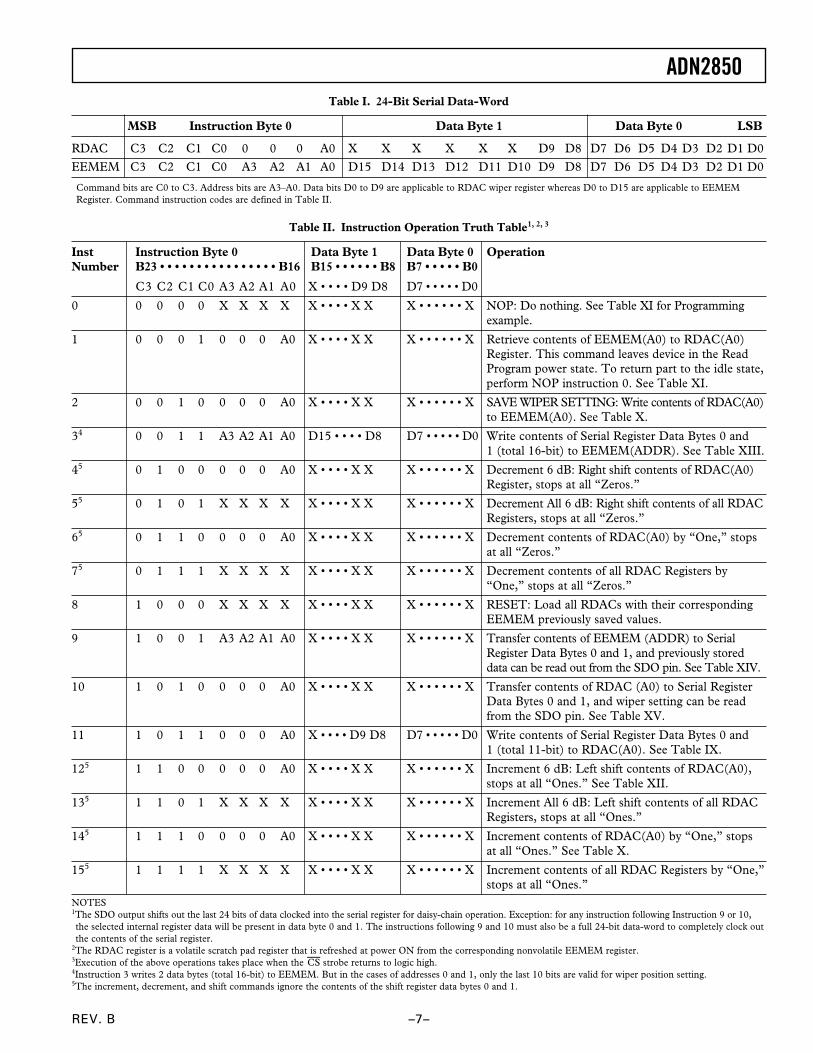
Table I. 24-Bit Serial Data-Word
MSB Instruction Byte 0 Data Byte 1 Data Byte 0 LSB
RDAC C3 C2 C1 C0 0 0 0 A0 X X X X X X D9 D8 D7 D6 D5 D4 D3 D2 D1 D0
EEMEM C3 C2 C1 C0 A3 A2 A1 A0 D15 D14 D13 D12 D11 D10 D9 D8 D7 D6 D5 D4 D3 D2 D1 D0
Command bits are C0 to C3. Address bits are A3–A0. Data bits D0 to D9 are applicable to RDAC wiper register whereas D0 to D15 are applicable to EEMEMRegister. Command instruction codes are defined in Table II.
Table II. Instruction Operation Truth Table1, 2, 3
Inst Instruction Byte 0 Data Byte 1 Data Byte 0 OperationNumber B23 • • • • • • • • • • • • • • • • B16 B15 • • • • • • B8 B7 • • • • • B0
C3 C2 C1 C0 A3 A2 A1 A0 X • • • • D9 D8 D7 • • • • • D0
0 0 0 0 0 X X X X X • • • • X X X • • • • • • X NOP: Do nothing. See Table XI for Programmingexample.
1 0 0 0 1 0 0 0 A0 X • • • • X X X • • • • • • X Retrieve contents of EEMEM(A0) to RDAC(A0)Register. This command leaves device in the ReadProgram power state. To return part to the idle state,perform NOP instruction 0. See Table XI.
2 0 0 1 0 0 0 0 A0 X • • • • X X X • • • • • • X SAVE WIPER SETTING: Write contents of RDAC(A0)to EEMEM(A0). See Table X.
34 0 0 1 1 A3 A2 A1 A0 D15 • • • • D8 D7 • • • • • D0 Write contents of Serial Register Data Bytes 0 and1 (total 16-bit) to EEMEM(ADDR). See Table XIII.
45 0 1 0 0 0 0 0 A0 X • • • • X X X • • • • • • X Decrement 6 dB: Right shift contents of RDAC(A0)Register, stops at all “Zeros.”
55 0 1 0 1 X X X X X • • • • X X X • • • • • • X Decrement All 6 dB: Right shift contents of all RDACRegisters, stops at all “Zeros.”
65 0 1 1 0 0 0 0 A0 X • • • • X X X • • • • • • X Decrement contents of RDAC(A0) by “One,” stopsat all “Zeros.”
75 0 1 1 1 X X X X X • • • • X X X • • • • • • X Decrement contents of all RDAC Registers by“One,” stops at all “Zeros.”
8 1 0 0 0 X X X X X • • • • X X X • • • • • • X RESET: Load all RDACs with their correspondingEEMEM previously saved values.
9 1 0 0 1 A3 A2 A1 A0 X • • • • X X X • • • • • • X Transfer contents of EEMEM (ADDR) to SerialRegister Data Bytes 0 and 1, and previously storeddata can be read out from the SDO pin. See Table XIV.
10 1 0 1 0 0 0 0 A0 X • • • • X X X • • • • • • X Transfer contents of RDAC (A0) to Serial RegisterData Bytes 0 and 1, and wiper setting can be readfrom the SDO pin. See Table XV.
11 1 0 1 1 0 0 0 A0 X • • • • D9 D8 D7 • • • • • D0 Write contents of Serial Register Data Bytes 0 and1 (total 11-bit) to RDAC(A0). See Table IX.
125 1 1 0 0 0 0 0 A0 X • • • • X X X • • • • • • X Increment 6 dB: Left shift contents of RDAC(A0),stops at all “Ones.” See Table XII.
135 1 1 0 1 X X X X X • • • • X X X • • • • • • X Increment All 6 dB: Left shift contents of all RDACRegisters, stops at all “Ones.”
145 1 1 1 0 0 0 0 A0 X • • • • X X X • • • • • • X Increment contents of RDAC(A0) by “One,” stopsat all “Ones.” See Table X.
155 1 1 1 1 X X X X X • • • • X X X • • • • • • X Increment contents of all RDAC Registers by “One,”stops at all “Ones.”
NOTES1The SDO output shifts out the last 24 bits of data clocked into the serial register for daisy-chain operation. Exception: for any instruction following Instruction 9 or 10,the selected internal register data will be present in data byte 0 and 1. The instructions following 9 and 10 must also be a full 24-bit data-word to completely clock outthe contents of the serial register.
2The RDAC register is a volatile scratch pad register that is refreshed at power ON from the corresponding nonvolatile EEMEM register.3Execution of the above operations takes place when the CS strobe returns to logic high.4Instruction 3 writes 2 data bytes (total 16-bit) to EEMEM. But in the cases of addresses 0 and 1, only the last 10 bits are valid for wiper position setting.5The increment, decrement, and shift commands ignore the contents of the shift register data bytes 0 and 1.
REV. B–8–
ADN2850OPERATIONAL OVERVIEWThe ADN2850 programmable resistor is designed to operate asa true variable resistor. The resistor wiper position is determinedby the RDAC register contents. The RDAC register acts as ascratch pad register which allows unlimited changes of resistancesettings. The scratch pad register can be programmed with anyposition setting using the standard SPI serial interface by loadingthe 24-bit data-word. The format of the data-word is that the first4 bits are instructions, the following 4 bits are addresses, and thelast 16 bits are data. Once a specific value is set, this value can besaved into a corresponding EEMEM register. During subsequentpower-ups, the wiper setting will automatically be loaded at thatvalue. Saving data to the EEMEM takes about 25 ms and con-sumes approximately 20 mA. During this time the shift registeris locked, preventing any changes from taking place. The RDY pinindicates the completion of this EEMEM saving process. Thereare also 13 two-bytes addresses, of user defined data that can bestored in EEMEM.
OPERATION DETAILThere are 16 instructions that facilitate users’ programmingneeds. Referring to Table II, the instructions are:
0. Do Nothing1. Restore EEMEM setting to RDAC2. Save RDAC setting to EEMEM3. Save user data or RDAC setting to EEMEM4. Decrement 6 dB5. Decrement all 6 dB6. Decrement one step7. Decrement all one step8. Reset all EEMEM settings to RDAC9. Read EEMEM to SDO
10. Read Wiper Setting to SDO11. Write data to RDAC12. Increment 6 dB13. Increment all 6 dB14. Increment one step15. Increment all one step
Tables VIII to XIV provide a few programming examples by usingsome of these instructions.
Scratch Pad and EEMEM ProgrammingThe basic mode of setting the programmable resistor wiper position(programming the scratch pad register) is done by loading theserial data input register with the instruction 11, the correspondingaddress, and the data. Since the scratch pad register is a standardlogic register, there is no restriction on the number of changesallowed. When the desired wiper position is determined, the user canload the serial data input register with the instruction 2, which storesthe setting into the corresponding EEMEM register. The EEMEMvalue can be changed at any time or permanently protected byactivating the WP command. Table III provides a programmingexample listing the sequence of serial data input (SDI) words andthe corresponding serial data output (SDO) in hexadecimal format.
Table III. Set and Save RDAC with Independent Datato EEMEM Registers
SDI SDO Action
B00100H XXXXXXH Loads data 100H into RDAC1 register,Wiper W1 moves to 1/4 full-scaleposition.
20xxxxH B00100H Saves copy of RDAC1 register contentinto corresponding EEMEM1 register.
B10200H 20xxxxH Loads 200H data into RDAC2 register,Wiper W2 moves to 1/2 full-scaleposition.
21xxxxH B10200H Saves copy of RDAC2 register contentsinto corresponding EEMEM2 register.
At system power ON, the scratch pad register is automaticallyrefreshed with the value previously saved in the correspondingEEMEM register. The factory preset EEMEM value is midscale.During operations, the scratch pad register can also be refreshedwith the current contents of the EEMEM registers in three differentways. First, executing instruction 1 retrieves the correspondingEEMEM value. Second, executing instruction 8 resets the EEMEMvalues of both channels. Finally, pulsing the PR pin also refreshesboth EEMEM settings. Operating the hardware control PRfunction, however, requires a complete pulse signal. When PRgoes low, the internal logic sets the wiper at midscale. TheEEMEM value will not be loaded until PR returns to high.
EEMEM ProtectionThe write-protect (WP) disables any changes of the scratch padregister contents regardless of the software commands, exceptthat the EEMEM setting can be refreshed and can overwrite theWP by using commands 1, 8, and PR pulse. To disable WP, it isrecommended to execute a NOP command before returningWP to logic high.
Linear Increment and Decrement CommandsThe increment and decrement commands (14, 15, 6, 7) are usefulfor linear step adjustment applications. These commands simplifymicrocontroller software coding by allowing the controller tojust send an increment or decrement command to the device. Theadjustment can be individually or gang controlled. For incre-ment command, executing instruction 14 will automatically move thewiper to the next resistance segment position. The master incrementinstruction 15 will move all resistor wipers up by one position.
Logarithmic Taper Mode Adjustment (6 dB/step)There are four programming instructions which provide thelogarithmic taper increment and decrement wiper position con-trol by either individual or gang control. 6 dB increment isactivated by instructions 12 and 13 and 6 dB decrement is acti-vated by instructions 4 and 5. For example, starting at zeroscale, executing 11 times the increment instruction 12 will movethe wiper in 6 dB per step from the 0% of the full-scale RWB tothe full-scale RWB. The 6 dB increment instruction doubles thevalue of the RDAC register contents each time the command isexecuted. When the wiper position is near the maximum setting,the last 6 dB increment instruction will cause the wiper to go tothe full-scale 1023-code position. Further 6 dB per incrementinstruction will no longer change the wiper position beyond itsfull-scale, Table IV.
6 dB step increment and decrement are achieved by shifting the bitinternally to the left and right, respectively. The following infor-mation explains the nonideal ±6 dB step adjustment at certain
REV. B
ADN2850
–9–
Using Additional Internal Nonvolatile EEMEMThe ADN2850 contains additional internal user storage registers(EEMEM) for saving constants and other 16-bit data. Table Vprovides an address map of the internal storage registers shownin the functional block diagram as EEMEM1, EEMEM2, andand 26 bytes (13 addresses 2 bytes each) of USER EEMEM.
Table V. EEMEM Address Map
EEMEMNumber Address EEMEM Content For
1 0000 RDAC11, 2
2 0001 RDAC23 0010 USER13
4 0011 USER2: : :15 1110 USER1316 1111 % Tolerance4
NOTES1RDAC data stored in EEMEM locations are transferred to their correspondingRDAC REGISTER at power-on, or when instructions 1, 8, and PR are executed.
2Execution of instruction 1 leaves the device in the read mode power consumptionstate. After the last instruction 1 is executed, the user should perform a NOP,instruction 0 to return the device to the low power idling state.
3USER <data> are internal nonvolatile EEMEM registers available to store andretrieve constants and other 16-bit information using instructions 3 and 9 respectively.
4Read only.
Calculating Actual Full-Scale ResistanceThe actual tolerance of the rated full-scale resistance RWB1 isstored in EEMEM register 15 during factory testing. The actualfull-scale resistance can therefore be calculated, which will bevaluable for tolerance matching or calibration. Notice this valueis read only, and the full-scale resistance of RWB2_FS matchesRWB1_FS, of typically 0.1%.
The tolerance in % is stored in the last 16 bits of data in EEMEMregister 15. The format is sign magnitude binary format with theMSB designates for sign (0 = positive and 1 = negative), the next7 MSB designate for the integer number, and the 8 LSB designatefor the decimal number. See Table VI.
Table VI. Tolerance in % from Rated Full-Scale Resistance
For example, if RWB_FS_RATED = 250 kΩ and the data is 00011100 0000 1111, RWB_FS_ACTUAL can be calculated as follows:
MSB: 0 = PositiveNext 7 MSB: 001 1100 = 288 LSB: 0000 1111 = 15 2–8 = 0.06% Tolerance = +28.06%
Thus, RWB_FS_ACTUAL = 320.15 kΩ
Bitsignmag
D15
sign
D14
26
D13
25
D12
24
D11
23
D10
22
D9
21
D8
20
D7
2-1
D6
2-2
D5
2-3
D4
2-4
D3
2-5
D2
2-6
D1
2-7
D0
2-8•
Sign 7 Bits for Integer Number Decimal
Point8 Bits for Decimal Number
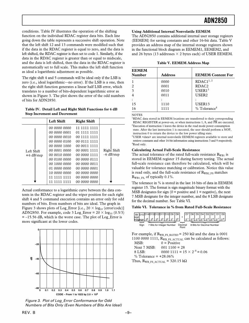
conditions. Table IV illustrates the operation of the shiftingfunction on the individual RDAC register data bits. Each linegoing down the table represents a successive shift operation. Notethat the left shift 12 and 13 commands were modified such thatif the data in the RDAC register is equal to zero, and the data isleft shifted, the RDAC register is then set to code 1. Similarly, if thedata in the RDAC register is greater than or equal to midscale,and the data is left shifted, then the data in the RDAC register isautomatically set to full scale. This makes the left shift functionas ideal a logarithmic adjustment as possible.
The right shift 4 and 5 commands will be ideal only if the LSB iszero (i.e., ideal logarithmic—no error). If the LSB is a one, thenthe right shift function generates a linear half LSB error, whichtranslates to a number of bits-dependent logarithmic error asshown in Figure 3. The plot shows the error of the odd numbersof bits for ADN2850.
Table IV. Detail Left and Right Shift Functions for 6 dBStep Increment and Decrement
Left Shift Right Shift
00 0000 0000 11 1111 111100 0000 0001 01 1111 111100 0000 0010 00 1111 111100 0000 0100 00 0111 111100 0000 1000 00 0011 111100 0001 0000 00 0001 111100 0010 0000 00 0000 111100 0100 0000 00 0000 011100 1000 0000 00 0000 001101 0000 0000 00 0000 000110 0000 0000 00 0000 000011 1111 1111 00 0000 000011 1111 1111 00 0000 0000
Actual conformance to a logarithmic curve between the data con-tents in the RDAC register and the wiper position for each rightshift 4 and 5 command execution contains an error only for oddnumbers of bits. Even numbers of bits are ideal. The graph inFigure 3 shows plots of Log_Error [i.e., 20 log10 (error/code)]ADN2850. For example, code 3 Log_Error = 20 log10 (0.5/3)= –15.56 dB, which is the worst case. The plot of Log_Error ismore significant at the lower codes.
CODE – From 1 to 1023 by 2.0 103
0
0
dB
–20
–40
–60
–800.1 0.2 0.3 0.4 0.5 0.6 0.7 0.8 0.9 1.0 1.1
Figure 3. Plot of Log_Error Conformance for OddNumbers of Bits Only (Even Numbers of Bits Are Ideal)
Right Shift–6 dB/step
Left Shift6 dB/step
REV. B–10–
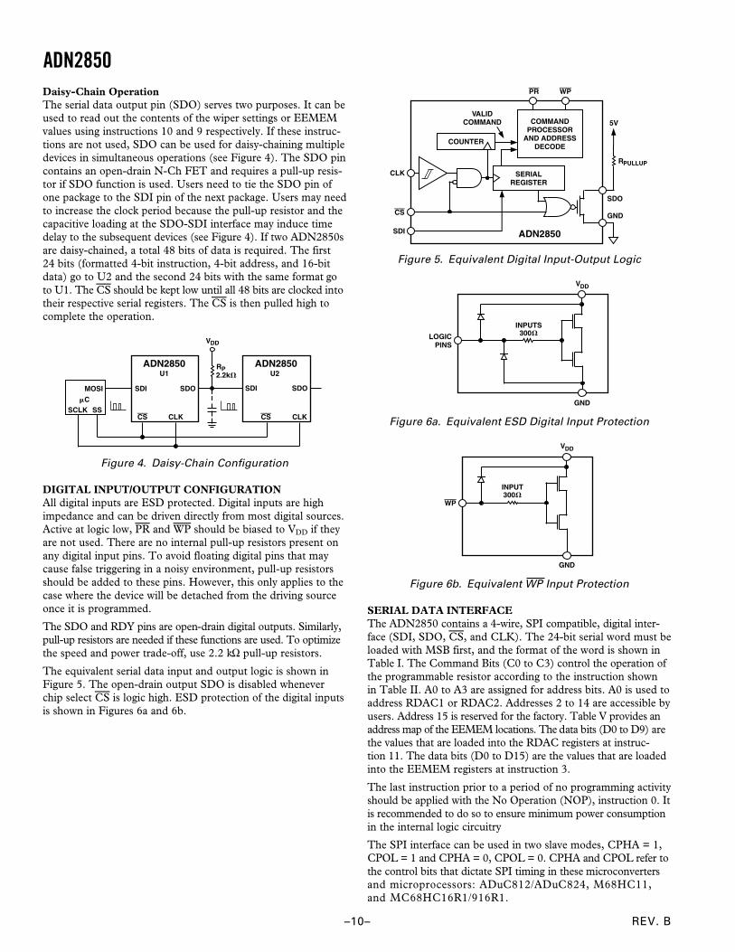
ADN2850Daisy-Chain OperationThe serial data output pin (SDO) serves two purposes. It can beused to read out the contents of the wiper settings or EEMEMvalues using instructions 10 and 9 respectively. If these instruc-tions are not used, SDO can be used for daisy-chaining multipledevices in simultaneous operations (see Figure 4). The SDO pincontains an open-drain N-Ch FET and requires a pull-up resis-tor if SDO function is used. Users need to tie the SDO pin ofone package to the SDI pin of the next package. Users may needto increase the clock period because the pull-up resistor and thecapacitive loading at the SDO-SDI interface may induce timedelay to the subsequent devices (see Figure 4). If two ADN2850sare daisy-chained, a total 48 bits of data is required. The first24 bits (formatted 4-bit instruction, 4-bit address, and 16-bitdata) go to U2 and the second 24 bits with the same format goto U1. The CS should be kept low until all 48 bits are clocked intotheir respective serial registers. The CS is then pulled high tocomplete the operation.
SDI SDO
CLK
VDD
RP2.2k
SDI SDO
CLKCS CS
U1ADN2850
CSS
MOSI
SCLK
U2ADN2850
Figure 4. Daisy-Chain Configuration
DIGITAL INPUT/OUTPUT CONFIGURATIONAll digital inputs are ESD protected. Digital inputs are highimpedance and can be driven directly from most digital sources.Active at logic low, PR and WP should be biased to VDD if theyare not used. There are no internal pull-up resistors present onany digital input pins. To avoid floating digital pins that maycause false triggering in a noisy environment, pull-up resistorsshould be added to these pins. However, this only applies to thecase where the device will be detached from the driving sourceonce it is programmed.
The SDO and RDY pins are open-drain digital outputs. Similarly,pull-up resistors are needed if these functions are used. To optimizethe speed and power trade-off, use 2.2 kΩ pull-up resistors.
The equivalent serial data input and output logic is shown inFigure 5. The open-drain output SDO is disabled wheneverchip select CS is logic high. ESD protection of the digital inputsis shown in Figures 6a and 6b.
VALIDCOMMAND
COUNTER
COMMANDPROCESSOR
AND ADDRESSDECODE
SERIALREGISTER
CLK
SDI
5V
RPULLUP
SDO
GND
PR WP
CS
ADN2850
Figure 5. Equivalent Digital Input-Output Logic
LOGICPINS
VDD
GND
INPUTS300
Figure 6a. Equivalent ESD Digital Input Protection
VDD
GND
INPUT300
WP
Figure 6b. Equivalent WP Input Protection
SERIAL DATA INTERFACEThe ADN2850 contains a 4-wire, SPI compatible, digital inter-face (SDI, SDO, CS, and CLK). The 24-bit serial word must beloaded with MSB first, and the format of the word is shown inTable I. The Command Bits (C0 to C3) control the operation ofthe programmable resistor according to the instruction shownin Table II. A0 to A3 are assigned for address bits. A0 is used toaddress RDAC1 or RDAC2. Addresses 2 to 14 are accessible byusers. Address 15 is reserved for the factory. Table V provides anaddress map of the EEMEM locations. The data bits (D0 to D9) arethe values that are loaded into the RDAC registers at instruc-tion 11. The data bits (D0 to D15) are the values that are loadedinto the EEMEM registers at instruction 3.
The last instruction prior to a period of no programming activityshould be applied with the No Operation (NOP), instruction 0. Itis recommended to do so to ensure minimum power consumptionin the internal logic circuitry
The SPI interface can be used in two slave modes, CPHA = 1,CPOL = 1 and CPHA = 0, CPOL = 0. CPHA and CPOL refer tothe control bits that dictate SPI timing in these microconvertersand microprocessors: ADuC812/ADuC824, M68HC11,and MC68HC16R1/916R1.
REV. B
ADN2850
–11–
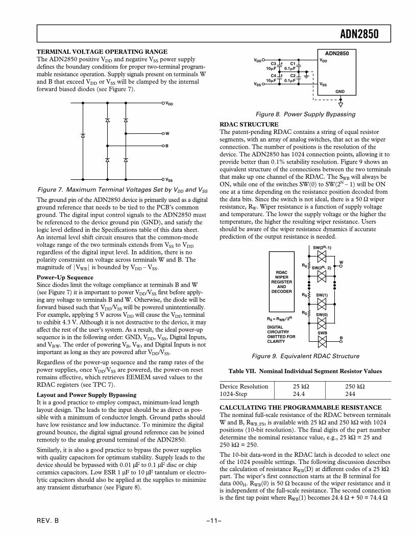
TERMINAL VOLTAGE OPERATING RANGEThe ADN2850 positive VDD and negative VSS power supplydefines the boundary conditions for proper two-terminal program-mable resistance operation. Supply signals present on terminals Wand B that exceed VDD or VSS will be clamped by the internalforward biased diodes (see Figure 7).
VSS
VDD
W
B
Figure 7. Maximum Terminal Voltages Set by VDD and VSS
The ground pin of the ADN2850 device is primarily used as a digitalground reference that needs to be tied to the PCB’s commonground. The digital input control signals to the ADN2850 mustbe referenced to the device ground pin (GND), and satisfy thelogic level defined in the Specifications table of this data sheet.An internal level shift circuit ensures that the common-modevoltage range of the two terminals extends from VSS to VDD
regardless of the digital input level. In addition, there is nopolarity constraint on voltage across terminals W and B. Themagnitude of |VWB| is bounded by VDD – VSS.
Power-Up SequenceSince diodes limit the voltage compliance at terminals B and W(see Figure 7) it is important to power VDD/VSS first before apply-ing any voltage to terminals B and W. Otherwise, the diode will beforward biased such that VDD/VSS will be powered unintentionally.For example, applying 5 V across VDD will cause the VDD terminalto exhibit 4.3 V. Although it is not destructive to the device, it mayaffect the rest of the user’s system. As a result, the ideal power-upsequence is in the following order: GND, VDD, VSS, Digital Inputs,and VB/W. The order of powering VB, VW, and Digital Inputs is notimportant as long as they are powered after VDD/VSS.
Regardless of the power-up sequence and the ramp rates of thepower supplies, once VDD/VSS are powered, the power-on resetremains effective, which retrieves EEMEM saved values to theRDAC registers (see TPC 7).
Layout and Power Supply BypassingIt is a good practice to employ compact, minimum-lead lengthlayout design. The leads to the input should be as direct as pos-sible with a minimum of conductor length. Ground paths shouldhave low resistance and low inductance. To minimize the digitalground bounce, the digital signal ground reference can be joinedremotely to the analog ground terminal of the ADN2850.
Similarly, it is also a good practice to bypass the power supplieswith quality capacitors for optimum stability. Supply leads to thedevice should be bypassed with 0.01 µF to 0.1 µF disc or chipceramics capacitors. Low ESR 1 µF to 10 µF tantalum or electro-lytic capacitors should also be applied at the supplies to minimizeany transient disturbance (see Figure 8).
ADN2850
C310F
C410F
+
+
C10.1F
C20.1F
VDD
VSS
GND
VDD
VSS
Figure 8. Power Supply Bypassing
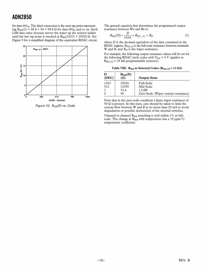
RDAC STRUCTUREThe patent-pending RDAC contains a string of equal resistorsegments, with an array of analog switches, that act as the wiperconnection. The number of positions is the resolution of thedevice. The ADN2850 has 1024 connection points, allowing it toprovide better than 0.1% setability resolution. Figure 9 shows anequivalent structure of the connections between the two terminalsthat make up one channel of the RDAC. The SWB will always beON, while one of the switches SW(0) to SW(2N – 1) will be ONone at a time depending on the resistance position decoded fromthe data bits. Since the switch is not ideal, there is a 50 Ω wiperresistance, RW. Wiper resistance is a function of supply voltageand temperature. The lower the supply voltage or the higher thetemperature, the higher the resulting wiper resistance. Usersshould be aware of the wiper resistance dynamics if accurateprediction of the output resistance is needed.
SW(1)
SW(0)
SWBB
RS
RS
SW(2N–1)
WSW(2N– 2)
RDACWIPER
REGISTERAND
DECODER
RS = RWB / 2N
RS
DIGITALCIRCUITRYOMITTED FORCLARITY
Figure 9. Equivalent RDAC Structure
Table VII. Nominal Individual Segment Resistor Values
Device Resolution 25 kΩ 250 kΩ1024-Step 24.4 244
CALCULATING THE PROGRAMMABLE RESISTANCEThe nominal full-scale resistance of the RDAC between terminalsW and B, RWB_FS, is available with 25 kΩ and 250 kΩ with 1024positions (10-bit resolution). The final digits of the part numberdetermine the nominal resistance value, e.g., 25 kΩ = 25 and250 kΩ = 250.
The 10-bit data-word in the RDAC latch is decoded to select oneof the 1024 possible settings. The following discussion describesthe calculation of resistance RWB(D) at different codes of a 25 kΩpart. The wiper’s first connection starts at the B terminal fordata 000H. RWB(0) is 50 Ω because of the wiper resistance and itis independent of the full-scale resistance. The second connectionis the first tap point where RWB(1) becomes 24.4 Ω + 50 = 74.4 Ω
REV. B–12–
ADN2850for data 001H. The third connection is the next tap point represent-ing RWB(2) = 48.8 + 50 = 98.8 Ω for data 002H and so on. EachLSB data value increase moves the wiper up the resistor ladderuntil the last tap point is reached at RWB(1023) = 25026 Ω. SeeFigure 9 for a simplified diagram of the equivalent RDAC circuit.
CODE – Decimal
25
15
00 1023256
RW
B (
D)
– k
512 768
10
5
20
RWB_FS = 25k
Figure 10. RWB(D) vs. Code
The general equation that determines the programmed outputresistance between Wx and Bx is:
R D
DR RWB WB FS W( ) = × +
1024 _ (1)
where D is the decimal equivalent of the data contained in theRDAC register, RWB_FS is the full-scale resistance between terminalsW and B, and RW is the wiper resistance.
For example, the following output resistance values will be set forthe following RDAC latch codes with VDD = 5 V (applies toRWB_FS = 25 kΩ programmable resistors):
Table VIII. RWB at Selected Codes (RWB_FS = 25 k)
D RWB(D)(DEC) () Output State
1023 25026 Full-Scale512 12550 Mid Scale1 74.4 1 LSB0 50 Zero-Scale (Wiper contact resistance)
Note that in the zero-scale condition a finite wiper resistance of50 Ω is present. In this state, care should be taken to limit thecurrent flow between W and B to no more than 20 mA to avoiddegradation or possible destruction of the internal switches.
Channel-to-channel RWB matching is well within 1% at full-scale. The change in RWB with temperature has a 35 ppm/°Ctemperature coefficient.
REV. B
Typical Performance Characteristics–ADN2850
–13–
CODE
36
160 1200200 400 600 800 1000
34
28
22
20
18
32
30
26
24
OH
MS
TPC 4. Wiper On-Resistance vs. Code
TEMPERATURE – C
4
–40 –20 0 20 100
CU
RR
EN
T –
A
40
3
2
1
0
–160 80
ISS @ VDD/VSS = 2.7V/0V
IDD @ VDD/VSS = 2.7V/0V
ISS @ VDD/VSS = 5V/0V
IDD @ VDD/VSS = 5V/0V
TPC 5. IDD vs. Temperature, RAB = 25 kΩ
0.25
FREQUENCY – Hz
0.0E+00
I DD
– m
A
0
0.20
0.15
0.10
0.05
2.0E+06 4.0E+06 6.0E+06 8.0E+06 1.0E+07 1.2E+07
MIDSCALE
FULL SCALE
ZERO SCALE
VDD/VSS = 5V/0VRAR = 25k
TPC 6. IDD vs. Clock Frequency, RAB = 25 kΩ
DIGITAL CODE
1.0
0 200 400 600 800
R-I
NL
ER
RO
R –
LS
B
0.8
0.6
0.2
–0.2
–0.6
0.4
0
–0.4
+25C–40C+85C
1000
TPC 1. R-INL vs. Code, TA = 40C, 25 C,85 C Overlay, RAB = 25 kΩ
DIGITAL CODE
0.4
0 200 400 600 1000–0.8
800
0.2
0
–0.2
–0.4
–0.6
R-D
NL
ER
RO
R –
LS
B
TPC 2. R-DNL vs. Code, TA = 40 C, 25 C,85 C Overlay, RAB = 25 kΩ
CODE – Decimal
120
100
20
–20
–80
RH
EO
ST
AT
MO
DE
TE
MP
CO
– p
pm
/C
10238967686405123842561280
80
60
40
0
–40
–60
VDD/VSS = 5.0V/0VTA = 25C
25k VERSION
250k VERSION
TPC 3. ∆RWB /∆T Rheostat Mode Tempco
REV. B–14–
ADN2850IW = IATA = 25C0.5V/DIV
RWB(D)
MIDSCALEEXPECTED
VALUE
50S/DIV
NO
RM
AL
IZE
D R
ES
ISTA
NC
E
TPC 7. Memory Restore During Power-On Reset
CS
CLK
VSDI
IDD20mA/DIV
4ms/DIV
5V/DIV
5V/DIV
5V/DIV
TPC 8. IDD vs. Time (Save) Program Mode
5V/DIV CS
CLK
SDI
IDD2mA/DIV
SUPPLY CURRENT RETURNS TO MINIMUM POWERCONSUMPTION IF INSTRUCTION 0 (NOP) ISEXECUTED IMMEDIATELY AFTER INSTRUCTION 1(READ EEMEM)
5V/DIV
5V/DIV
4ms/DIV
TPC 9. IDD vs. Time (Read) Program Mode
CODE – Decimal
100
1
0.011024
TH
EO
RE
TIC
AL
– I W
B_M
AX
– m
A
0.1
10
RWB_FS = 25k
RWB_FS = 250k
896768640512384128 2560
TA = 25C
TPC 10. IWB_MAX vs. Code
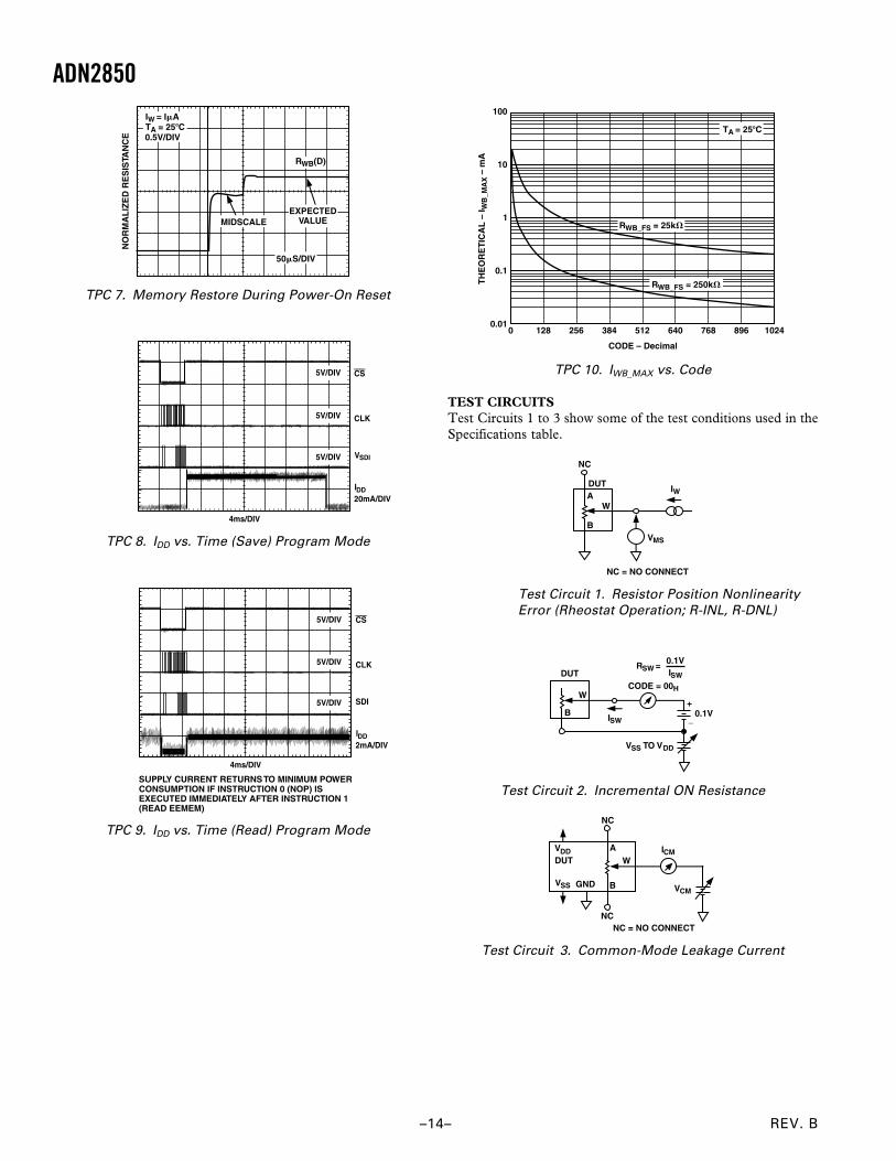
TEST CIRCUITSTest Circuits 1 to 3 show some of the test conditions used in theSpecifications table.
W
B
NC
IWDUT
VMS
NC = NO CONNECT
A
Test Circuit 1. Resistor Position NonlinearityError (Rheostat Operation; R-INL, R-DNL)
+
_
DUTCODE = 00H
0.1V
VSS TO VDD
RSW = 0.1VISW
ISW
W
B
Test Circuit 2. Incremental ON Resistance
DUT
VSS
ICM W
B
VDD
NC
NC
VCM GND
A
NC = NO CONNECT
Test Circuit 3. Common-Mode Leakage Current
REV. B
ADN2850
–15–
Table XII. Using Left Shift by One to Increment 6 dB Steps
SDI SDO Action
C0XXXXH XXXXXXH Moves wiper 1 to double the presentdata contained in RDAC1 register.
C1XXXXH C0XXXXH Moves wiper 2 to double the presentdata contained in RDAC2 register.
Table XIII. Storing Additional User Data in EEMEM
SDI SDO Action
32AAAAH XXXXXXH Stores data AAAAH into spare EEMEMlocation USER1. (Allowable to addressin 13 locations with maximum 16 bitsof data).
335555H 32AAAAH Stores data 5555H into spare EEMEMlocation USER2. (Allowable to addressin 13 locations with maximum 16 bitsof data).
Table XIV. Reading Back Data From Various Memory Locations
SDI SDO Action
92XXXXH XXXXXXH Prepares data read from USER1location.
00XXXXH 92AAAAH NOP instruction 0 sends 24-bit wordout of SDO where the last 16 bitscontain the contents of USER1 location.NOP command ensures device returnsto idle power dissipation state.
Table XV. Reading Back Wiper Setting
SDI SDO Action
B00200H XXXXXXH Sets RDAC1 to midscale.C0XXXXH B00200H Doubles RDAC1 from midscale to
full-scale.A0XXXXH C0XXXXH Prepares reading wiper setting from
RDAC1 register.XXXXXXH A003FFH Readback full-scale value from RDAC1
register.
Analog Devices offers a user-friendly ADN2850EVAL evaluationkit that can be controlled by a personal computer through the printerport. The driving program is self-contained, so no programminglanguages or skills are needed.
PROGRAMMING EXAMPLESThe following programming examples illustrate the typical sequenceof events for various features of the ADN2850. Users should referto Table II for the instructions and data-word format. The instruc-tion numbers, addresses, and data appearing at SDI and SDO pinsare displayed in hexadecimal format in the following examples.
Table IX. Scratch Pad Programming
SDI SDO Action
B00100H XXXXXXH Loads data 100H into RDAC1 register,Wiper W1 moves to 1/4 full-scaleposition.
B10200H B00100H Loads data 200H into RDAC2 register,Wiper 2 moves to 1/2 full-scale position.
Table X. Incrementing RDAC Followed by Storingthe Wiper Setting to EEMEM
SDI SDO Action
B00100H XXXXXXH Loads data 100H into RDAC1 register,Wiper W1 moves to 1/4 full-scale position.
E0XXXXH B00100H Increments RDAC1 register by one to 101H.E0XXXXH E0XXXXH Increments RDAC1 register by one to 102H.
Repeat the increment command –(E0XXXXH) until desired wiperposition is reached
20XXXXH XXXXXXH Saves RDAC1 data into EEMEM1Optionally tie WP to GND to protectEEMEM values
Table XI. Restoring EEMEM Values to RDAC Registers
EEMEM values for RDACs can be restored by: Power-On,Strobing PR pin or Programming shown below.
SDI SDO Action
10XXXXH XXXXXXH Restores EEMEM1 value to RDAC1register.
00XXXXH 100100H NOP. Recommended step to minimizepower consumption.
8XXXXXH 00XXXXH Reset EEMEM1 and EEMEM2values to RDAC1 and RDAC2 registersrespectively.
REV. B–16–
ADN2850
Q1
–5V
Q2
V1 V2 CPRCTHERMISTOR
LOGAVERAGEPOWER
VT COMPENSATION
AD623IN AMP
RG
IREFIPD
10nF
TIA LPF0.75 BIT RATE
POSTAMP
CDRDATA
CLOCK
LOG AMP
W1 W2VDD
GNDB1 B2VSS
(1 + 100k/RG) (V2 – V1)
ADN2850
Figure 12. Conceptual Incoming Optical Power Monitoring Circuit
APPLICATIONSOptical Transmitter Calibration with ADN2841Together with the multirate 2.7 Gbps Laser Diode Driver ADN2841,the ADN2850 forms an optical supervisory system where the dualprogrammable resistors are used to set the laser average opticalpower and extinction ratio (see Figure 11). The ADN2850 isparticularly ideal for the optical parameter settings because of itshigh resolution, compact footprint, and superior temperaturecoefficient characteristics.
The ADN2841 is a 2.7 Gbps laser diode driver that uses a uniquecontrol algorithm to manage both the laser average power andextinction ratio after the laser initial factory calibration. It stabilizesthe laser data transmission by continuously monitoring its opticalpower, and correcting the variations caused by temperature andthe laser degradation over time. In the ADN2841, the IMPD monitorsthe laser diode current. Through its dual-loop power and extinctionratio control, calibrated by the ADN2850, the internal drivercontrols the bias current IBIAS and consequently the average power.It also regulates the modulation current IMODP by changing themodulation current linearly with slope efficiency. Any changes inthe laser threshold current or slope efficiency are therefore com-pensated. As a result, this optical supervisory system minimizes thelaser characterization efforts and enables designers to apply com-parable lasers from multiple sources.
Incoming Optical Power MonitoringThe ADN2850 comes with a pair of matched diode connectedPNPs, Q1 and Q2, that can be used to configure an incoming opticalpower monitoring function. With a reference current source, aninstrumentation amplifier, and a logarithmic amplifier, this featurecan be used to monitor the optical power by knowing the dcaverage photodiode current from the following relationships:
V =V =V1 BE1 T In
II
C
S
1
1(2)
V =V =V I2 BE2 T n
II
C
S
2
2(3)
CS
CLK
SDI
RDAC1 W1
B1EEMEM
ADN2841
PSET
ERSET
IMODP
IBIAS
IMPD
DIN
DIN
Q
IDTO
NE
DINDINQ
IDTONE
RDAC2 W2
B2EEMEM
CONTROL
ADN2850
VCC VCC
Figure 11. Optical Supervisory System
Knowing IC1 = a1 IPD, IC2 = a2 IREF, and Q1– Q2 are matched,therefore a and IS are matched. Combining Equations 2 and 3theoretically yields:
V –V =V In T2 1
IIREF
PD
(4)
Where IS1 and IS2 are saturation currentV1, V2 are VBE, base-emitted voltages of the diode connectortransistorsVT is the thermal voltage, which is equal to k × T/q. VT = 26 mV at 25°Ck = Boltzmann’s constant = 1.38E–23 Joules/Kelvinq = electron charge = 1.6E–19 coulombT = temperature in KelvinIPD = photodiode currentIREF = reference current
Figure 12 shows such a conceptual circuit.
REV. B
ADN2850
–17–
The output voltage represents the average incoming optical power.The output voltage of the log stage does not have to be accuratefrom device to device, as the responsivity of the photodiode willchange between devices. An op amp stage is shown after the logamp stage, which compensates for VT variation over temperature.
Equation 4 is ideal. If the reference current is 1 mA at roomtemperature, characterization shows that there is an additional30 mV offset between V2 and V1. A curve fit approximation yields
V V = 0.026 In
0.0012 — 1 ×
+IPD
0 03. (5)
Such offset is believed to be caused by the transistors self-heatingand the thermal gradient effect. As seen in Figure 13, the errorbetween an approximation and the actual performance ranges isless than 0% to –4% from 0.1 mA to 0.1 A.
0.30
0.25
0.20
0.15
0.10
0.05
0
12
9
6
3
0
–3
–61.E-07 1.E-06 1.E-05 1.E-04 1.E-03
V2
– V
1 –
V
AP
PR
OX
IMAT
ING
ER
RO
R –
%
IPD – A
IREF = 1mATA = 25C
DEVICE 1DEVICE 2DEVICE 3CURVE FIT
ERROR
Figure 13. Typical V2 – V1 vs. IPD at IREF = 1 mAand TA = 25°C
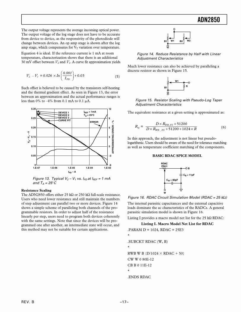
Resistance ScalingThe ADN2850 offers either 25 kΩ or 250 kΩ full-scale resistance.Users who need lower resistance and still maintain the numbersof step adjustment can parallel two or more devices. Figure 14shows a simple scheme of paralleling both channels of the pro-grammable resistors. In order to adjust half of the resistancelinearly per step, users need to program both devices coherentlywith the same settings. Note that since the devices will be pro-grammed one after another, an intermediate state will occur, andthis method may not be suitable for certain applications.
B1 W1 W2B2
Figure 14. Reduce Resistance by Half with LinearAdjustment Characteristics
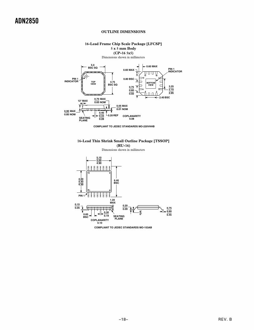
Much lower resistance can also be achieved by paralleling adiscrete resistor as shown in Figure 15.
B1
W1
R
Figure 15. Resistor Scaling with Pseudo-Log TaperAdjustment Characteristics
The equivalent resistance at a given setting is approximated as:
R =
D Req
WB_FS× +× + + ×
5120051200 1024D R RWB FS_
(6)
In this approach, the adjustment is not linear but pseudo-logarithmic. Users should be aware of the need for tolerance matchingas well as temperature coefficient matching of the components.
BASIC RDAC SPICE MODEL
RDAC25k
W
CW = 80pF
CB = 11pF
B
Figure 16. RDAC Circuit Simulation Model (RDAC = 25 kΩ)
The internal parasitic capacitances and the external capacitiveloads dominate the ac characteristics of the RADCs. A generalparasitic simulation model is shown in Figure 16.
Listing I provides a macro model net list for the 25 kΩ RDAC:
Listing I. Macro Model Net List for RDAC
.PARAM D = 1024, RDAC = 25E3
*
.SUBCKT RDAC (W, B)
*
RWB W B D/1024 RDAC 50
CW W 0 80E-12
CB B 0 11E-12
*
.ENDS RDAC
REV. B–18–
ADN2850OUTLINE DIMENSIONS
16-Lead Frame Chip Scale Package [LFCSP]5 x 5 mm Body
(CP-16 5x5)Dimensions shown in millimeters
16
5
13
89
12 1
4
BOTTOMVIEW
3.253.102.95
0.750.600.50
0.80 BSC
2.40 BSC
0.400.330.28
12 MAX
0.20 REFSEATINGPLANE
PIN 1INDICATOR TOP
VIEW
5.0BSC SQ
4.75BSC SQ
0.60 MAX0.60 MAX
0.05 MAX0.01 NOM
0.70 MAX0.65 NOM
PIN 1INDICATOR
COPLANARITY0.08
0.90 MAX0.85 NOM
COMPLIANT TO JEDEC STANDARDS MO-220VHHB
16-Lead Thin Shrink Small Outline Package [TSSOP](RU-16)
Dimensions shown in millimeters
16 9
81
PIN 1
SEATINGPLANE
80
4.504.404.30
6.40BSC
5.105.004.90
0.65BSC
0.150.05
1.20MAX
0.200.09 0.75
0.600.45
0.300.19
COPLANARITY0.10
COMPLIANT TO JEDEC STANDARDS MO-153AB
REV. B
ADN2850
–19–
Revision HistoryLocation Page
9/02—Data sheet changed from REV. A to REV. B.
Changes to GENERAL DESCRIPTION . . . . . . . . . . . . . . . . . . . . . . . . . . . . . . . . . . . . . . . . . . . . . . . . . . . . . . . . . . . . . . . . . . . . .1
Changes to ELECTRICAL CHARACTERISTICS . . . . . . . . . . . . . . . . . . . . . . . . . . . . . . . . . . . . . . . . . . . . . . . . . . . . . . . . . . . . .2
Changes to Calculating Actual Full-Scale Resistance section . . . . . . . . . . . . . . . . . . . . . . . . . . . . . . . . . . . . . . . . . . . . . . . . . . . . . . 9
Changes to Table VI . . . . . . . . . . . . . . . . . . . . . . . . . . . . . . . . . . . . . . . . . . . . . . . . . . . . . . . . . . . . . . . . . . . . . . . . . . . . . . . . . . . . .9
Updated OUTLINE DIMENSIONS . . . . . . . . . . . . . . . . . . . . . . . . . . . . . . . . . . . . . . . . . . . . . . . . . . . . . . . . . . . . . . . . . . . . . . .18

C02
660–
0–9/
02(B
)P
RIN
TE
D IN
U.S
.A.
–20–