Embed Size (px)
Citation preview
[email protected] Paper No. 26 571-272-7822 Entered: January 17, 2017
UNITED STATES PATENT AND TRADEMARK OFFICE ____________
BEFORE THE PATENT TRIAL AND APPEAL BOARD
____________
SAMSUNG ELECTRONICS CO., LTD, Petitioner,
v.
ELBRUS INTERNATIONAL LIMITED, Patent Owner. ____________
Case IPR2015-01524
Patent 6,366,130 ____________
Before JUSTIN T. ARBES, JEFFREY W. ABRAHAM, and DANIEL J. GALLIGAN, Administrative Patent Judges.
ABRAHAM, Administrative Patent Judge.
FINAL WRITTEN DECISION 35 U.S.C. § 318(a)
Case IPR2015-01524 Patent 6,366,130
2
I. INTRODUCTION
Samsung Electronics Co., Ltd. (“Petitioner”) filed a Petition seeking
inter partes review of claims 1–3, 5–7, and 9 of U.S. Patent No. 6,366,130
B1 (Ex. 1001, “the ’130 patent”), as amended by Inter Partes
Reexamination Certificate No. US 6,366,130 C1 (“Reexam. Cert.”). Paper 1
(“Pet.”). Elbrus International Limited (“Patent Owner”) filed a Preliminary
Response to the Petition. Paper 8. On January 19, 2016, we instituted an
inter partes review of claims 1–3, 5–7, and 9. Paper 9 (“Dec. on Inst.”).
After institution, Patent Owner filed a Patent Owner Response (Paper
12, “PO Resp.”), and Petitioner filed a Reply (Paper 16, “Reply”). An oral
hearing was held on October 18, 2016, and a transcript of the hearing has
been entered into the record of the proceeding as Paper 25 (“Tr.”).
We have jurisdiction under 35 U.S.C. § 6. This Final Written
Decision is issued pursuant to 35 U.S.C. § 318(a). For the reasons that
follow, we determine that Petitioner has shown by a preponderance of the
evidence that claims 1, 2, 5–7, and 9 are unpatentable.
II. BACKGROUND
A. Related Proceedings
The parties identify Cascades Computer Innovation, LLC. v. Samsung
Electronics Co., Ltd., Case No. 1-14-cv-05691 (N.D. Ill). Pet. 1–2; Paper 4,
3.
B. The ’130 Patent
The ’130 patent, titled “High Speed Low Power Data Transfer
Scheme,” issued on April 2, 2002, with a reexamination certificate issuing
on August 4, 2014. The ’130 patent is directed to a “high speed and low
power [complementary metal-oxide semiconductor (CMOS)] data transfer
Case IPR2015-01524 Patent 6,366,130
3
arrangement that includes two active pull up/pull down bus drivers, a
differential bus that precharges to a specific voltage level and a latched
differential sense amplifier that serves as a bus receiver.” Ex. 1001, 1:24–
28, Fig. 1. In one embodiment, the latching sense amplifier is arranged as a
“cross coupled latched amplifier.” Id. at 1:36–38, Fig. 2. The ’130 patent
explains that its data transfer scheme can operate at increased speeds due to,
inter alia, precharging the buses to a specific level (Vpr) between ground
and Vdd. Id. at 2:23–38, 3:17–55.
C. Illustrative Claim
Petitioner challenges claims 1–3, 5–7, and 9. Claim 1 is the only
independent claim challenged and is reproduced below.
1. A data transfer arrangement comprising:
two bus drivers;
a voltage precharge source;
a differential bus coupled to the bus drivers and to the voltage precharge source; aid
a latching sense amplifier coupled to the differential bus;
wherein the latching sense amplifier comprises:
a first stage including a cross-coupled latch coupled to a differential data bus; and
an output stage coupled to an output of said first stage;
wherein the output of the first stage is coupled to an input of the output stage;
wherein the differential bus and the differential data bus are precharge to a voltage Vpr between Vdd and ground, where Vpr=K*Vdd, and K is a precharging voltage factor.
Id. at 4:2–17.
Case IPR2015-01524 Patent 6,366,130
4
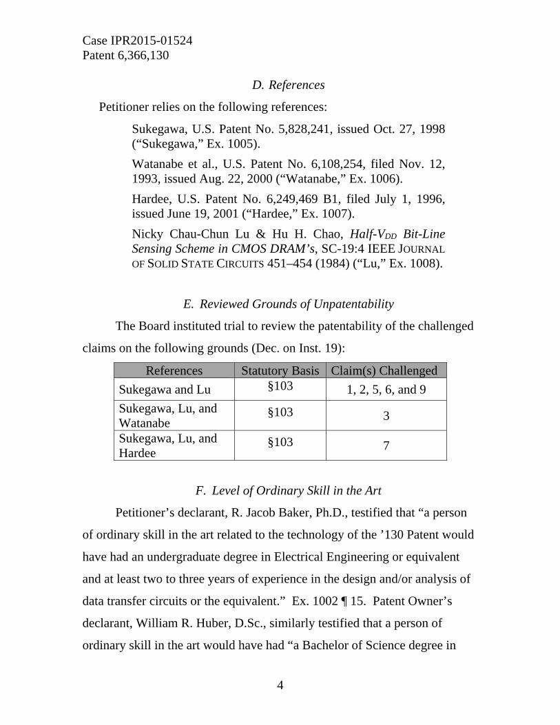
D. References
Petitioner relies on the following references:
Sukegawa, U.S. Patent No. 5,828,241, issued Oct. 27, 1998 (“Sukegawa,” Ex. 1005).
Watanabe et al., U.S. Patent No. 6,108,254, filed Nov. 12, 1993, issued Aug. 22, 2000 (“Watanabe,” Ex. 1006).
Hardee, U.S. Patent No. 6,249,469 B1, filed July 1, 1996, issued June 19, 2001 (“Hardee,” Ex. 1007).
Nicky Chau-Chun Lu & Hu H. Chao, Half-VDD Bit-Line Sensing Scheme in CMOS DRAM’s, SC-19:4 IEEE JOURNAL
OF SOLID STATE CIRCUITS 451–454 (1984) (“Lu,” Ex. 1008).
E. Reviewed Grounds of Unpatentability
The Board instituted trial to review the patentability of the challenged
claims on the following grounds (Dec. on Inst. 19):
References Statutory Basis Claim(s) Challenged
Sukegawa and Lu §103 1, 2, 5, 6, and 9
Sukegawa, Lu, and Watanabe
§103 3
Sukegawa, Lu, and Hardee
§103 7
F. Level of Ordinary Skill in the Art
Petitioner’s declarant, R. Jacob Baker, Ph.D., testified that “a person
of ordinary skill in the art related to the technology of the ’130 Patent would
have had an undergraduate degree in Electrical Engineering or equivalent
and at least two to three years of experience in the design and/or analysis of
data transfer circuits or the equivalent.” Ex. 1002 ¶ 15. Patent Owner’s
declarant, William R. Huber, D.Sc., similarly testified that a person of
ordinary skill in the art would have had “a Bachelor of Science degree in
Case IPR2015-01524 Patent 6,366,130
5
Electrical Engineering or an equivalent field, as well as at least 2 years of
experience designing and analyzing data transfer or equivalent circuits.” Ex.
2004 ¶ 27.
We credit the testimony provided by the declarants for both parties
and hold that one of ordinary skill in the art would have possessed an
undergraduate degree in electrical engineering or equivalent field and at
least two years of experience in the design and/or analysis of data transfer or
equivalent circuits. This level of ordinary skill is reflected not only by the
information presented by the parties, but also by the prior art of record.
Okajima v. Bourdeau, 261 F.3d 1350, 1355 (Fed. Cir. 2001) (the prior art
itself can reflect the appropriate level of ordinary skill in the art).
III. ANALYSIS
A. Claim Construction
In an inter partes review, claim terms in an unexpired patent are
interpreted according to their broadest reasonable construction in light of the
specification of the patent in which they appear. 37 C.F.R. § 42.100(b); see
Cuozzo Speed Techs., LLC v. Lee, 136 S. Ct. 2131, 2144–46 (2016)
(upholding the use of the broadest reasonable interpretation standard). In
applying a broadest reasonable construction, claim terms generally are given
their ordinary and customary meaning, as would be understood by one of
ordinary skill in the art in the context of the entire disclosure. See In re
Translogic Tech., Inc., 504 F.3d 1249, 1257 (Fed. Cir. 2007).
Based on the parties’ post-issuance arguments (Reply 2–6; PO Resp.
20–24; Tr. 33:25–34:6), we address the proper interpretation of the claim
term “bus,” which we discuss below. No other express claim construction is
Case IPR2015-01524 Patent 6,366,130
6
necessary. See Vivid Techs., Inc. v. Am. Sci. & Eng’g, Inc., 200 F.3d 795,
803 (Fed. Cir. 1999) (“[O]nly those terms need be construed that are in
controversy, and only to the extent necessary to resolve the controversy.”).
“bus”
Claim 1 requires a “differential bus” and a “differential data bus.”
The ’130 patent does not expressly define “bus.” Petitioner contends that
“bus” is a term of art and should be given its plain and ordinary meaning.
Reply 2. Relying on the 1994 IEEE Standard Glossary of Computer
Hardware Terminology, Petitioner contends that a “bus” is understood to be
“one or more conductors that are used for the transmission of signals, data,
or power.” Ex. 1010, 13; Reply 2. Petitioner contends that this definition is
consistent with the use of the term in the ’130 patent and supported by Dr.
Baker’s testimony. Reply 2–3 (citing Ex. 1001, Fig. 1, 2:1–22, 4:2–18; Ex.
2003, 49:4–9, 49:15–17). Patent Owner, relying on the June 2013 JEDEC
Dictionary of Terms for Solid-State Technology, argues that a “bus” is
defined as “[a] common path along which power or signals travel from one
or several sources to one or several destinations.” Ex. 2005, 27;1 see PO
Resp. 21–22 & n.2.
We agree with, and adopt, Petitioner’s interpretation of the plain and
ordinary meaning of bus, as informed by the 1994 IEEE Standard Glossary
of Computer Hardware Terminology. It is well settled that judges may
consult dictionary definitions when construing claim terms so long as the
dictionary definition does not contradict any definition found in or
ascertained by a reading of the patent documents. Vitronics Corp. v.
1 Page numbers for this exhibit refer to the page numbers in the top right or left corner of each page of the exhibit.
Case IPR2015-01524 Patent 6,366,130
7
Conceptronic, Inc., 90 F.3d 1576, 1585 n.6 (Fed. Cir. 1996). Petitioner’s
proposed construction satisfies this criteria, because, as noted above, the
’130 patent does not include a definition of “bus,” and the ’130 patent uses
the claimed buses as part of its data transfer arrangement, wherein the bus
lines are charged to a particular voltage and used to transfer data. Ex. 1001,
2:12–38.
We do not adopt Patent Owner’s proposed interpretation because, as
Petitioner argues and Patent Owner acknowledges, the reference upon which
Patent Owner relies was published several years after the filing date of the
application leading to the ’130 patent. Tr. 35:7–13; see also Reply 3
(Petitioner arguing that Patent Owner’s interpretation of “bus” is flawed
because it is from a document dated over 13 years after the alleged invention
date of the ’130 patent). Additionally, Dr. Huber elaborates on Patent
Owner’s understanding of the term “bus,” stating that a bus, unlike a node,
has a span, and acts like a bridge between two points. Ex. 2004 ¶ 59, 62.
Dr. Huber, however, offers no underlying facts or data to support this
interpretation. Pursuant to 37 C.F.R. § 42.65(a), such testimony is entitled
to little or no weight. Also, neither definition from the parties’ technical
dictionaries includes a “span” requirement for the term. See Exs. 1010,
2005; Tr. 35:14–17.
We thus find the broadest reasonable interpretation of “bus” in light of
the ’130 patent Specification is “one or more conductors that are used for the
transmission of signals, data, or power.” Ex. 1010, 13; Reply 2.
Case IPR2015-01524 Patent 6,366,130
8
B. Principles of Law
To prevail in this inter partes review of the challenged claims,
Petitioner must prove unpatentability by a preponderance of the evidence.
35 U.S.C. § 316(e); 37 C.F.R. § 42.1(d).
A patent claim is unpatentable under 35 U.S.C. § 103(a) if the
differences between the claimed subject matter and the prior art are such that
the subject matter, as a whole, would have been obvious at the time the
invention was made to a person having ordinary skill in the art to which said
subject matter pertains. KSR Int’l Co. v. Teleflex Inc., 550 U.S. 398, 406
(2007). The question of obviousness is resolved on the basis of underlying
factual determinations, including: (1) the scope and content of the prior art;
(2) any differences between the claimed subject matter and the prior art;
(3) the level of skill in the art; and (4) objective evidence of nonobviousness.
Graham v. John Deere Co., 383 U.S. 1, 17–18 (1966).
A party that petitions the Board for a determination of obviousness
must show that “a skilled artisan would have been motivated to combine the
teachings of the prior art references to achieve the claimed invention, and
that the skilled artisan would have had a reasonable expectation of success in
doing so.” Procter & Gamble Co. v. Teva Pharms. USA, Inc., 566 F.3d 989,
994 (Fed. Cir. 2009) (quoting Pfizer, Inc. v. Apotex, Inc., 480 F.3d 1348,
1361 (Fed. Cir. 2007)).
C. References
1. Sukegawa
Sukegawa discloses a “signal transmission circuit which enables the
distance of signal transmission . . . to be increased, while the signal delay
and power consumption are reduced.” Ex. 1005, Abstract. Sukegawa
Case IPR2015-01524 Patent 6,366,130
9
teaches that “the signal is amplified and transmitted by means of the positive
feedback of an intermediate amplifier circuit having input/output shared
terminals.” Id. at 1:12–15. Sukegawa provides circuit diagrams illustrating,
and corresponding descriptions in the specification describing, the specific
configuration of the various components of its transmission circuit. See id.
at 6:35–9:50, Figs. 1–7.
2. Watanabe
Watanabe discloses a “[dynamic random access memory (DRAM)]
having means which can transfer data at a sufficiently high speed.” Ex.
1006, 1:64–65. Watanabe’s data transfer circuit contains differential
amplifier circuit 10, equalizing circuit 11, data latch circuit 12, pairs of first
data lines 13 and second data lines 14, and pair of data output lines 15. Id. at
3:41–44, Fig. 1. In one embodiment, data latch circuit 12 comprises three n-
channel MOS transistors and five p-channel MOS transistors, arranged as
shown in Figure 7 of Watanabe. Id. at 4:13–19, Fig. 7. Watanabe explains
that its transfer circuit is an improvement over conventional data transfer
control systems because data transfer can occur without having to take the
time to equalize its data lines. Id. at 2:52–56.
3. Hardee
Hardee discloses a “sense amplifier for a very high density integrated
circuit memory using CMOS technology.” Ex. 1007, Abstract. Hardee
further discloses a preferred sense amplifier containing, inter alia, “N
channel devices having their source-drain paths coupled in series.” Id. at
6:28–46 (referring to transistors 128, 130, 132, 134), Fig. 5. Hardee states
that these transistors “provide isolation and thereby lower the stand-by
Case IPR2015-01524 Patent 6,366,130
10
current or normal current drain of a sense amplifier where no writing
operation is to occur.” Id. at 12:2–4.
4. Lu
Lu discloses “a sensing scheme for CMOS DRAM’s in which the bit
line is precharged to half VDD” and states that “half-VDD bit-line sensing has
several unique advantages . . . when compared to the full-VDD bit-line
sensing scheme used for NMOS memory arrays or the grounded bit-line
sensing scheme for PMOS arrays in CMOS DRAM’s.” Ex. 1008, 451.
According to Lu, these advantages include increased speed and reduced
power consumption. Id. at 453.
D. Analysis of Grounds of Unpatentability
1. Claims 1, 2, 5, 6, and 9
Petitioner asserts that the subject matter of claims 1, 2, 5, 6, and 9
would have been obvious over Sukegawa in view of Lu. Pet. 14–33.
Petitioner provides detailed explanations, including claim charts and the
declaration of Dr. Baker, to show how Sukegawa and Lu disclose or suggest
each limitation of claims 1, 2, 5, 6, and 9. In our Decision on Institution, we
determined that Petitioner had made a threshold showing that the prior art
discloses or suggests all limitations of these claims sufficient for us to
conclude that there was a reasonable likelihood that Petitioner would prevail
in showing that the subject matter of the challenged claims would have been
obvious in view of Sukegawa and Lu. Dec. on Inst. 7–14.
In its Response, Patent Owner disputes that Sukegawa and Lu disclose
two limitations of claim 1, and argues that “Sukegawa teaches away from
the ’130 invention” and that “Petitioner’s solution is unworkable in
practice.” PO Resp. 17–18. Patent Owner also argues that Petitioner fails to
Case IPR2015-01524 Patent 6,366,130
11
show that Sukegawa and Lu disclose or suggest precharging the differential
bus to a voltage that “is less than a logic high voltage and greater than a
logic low voltage,” as required by dependent claim 5. Id. at 37–42. For the
remaining dependent claims, Patent Owner argues that because the subject
matter of claim 1 would not have been obvious, the subject matter of the
dependent claims also would not have been obvious. Id. at 45. Finally,
Patent Owner argues that Petitioner improperly relies on hindsight to
establish obviousness. Id. at 43–45.
a. The Disputed Limitations of Claim 1
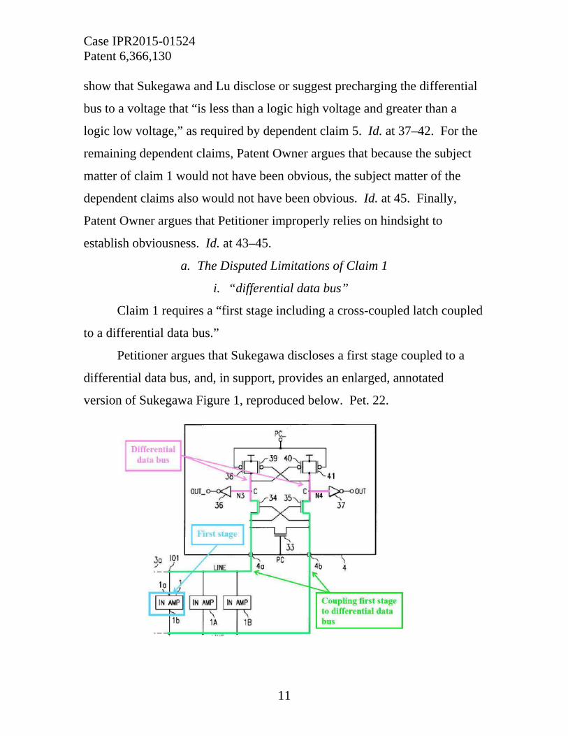
i. “differential data bus”
Claim 1 requires a “first stage including a cross-coupled latch coupled
to a differential data bus.”
Petitioner argues that Sukegawa discloses a first stage coupled to a
differential data bus, and, in support, provides an enlarged, annotated
version of Sukegawa Figure 1, reproduced below. Pet. 22.
Case IPR2015-01524 Patent 6,366,130
12
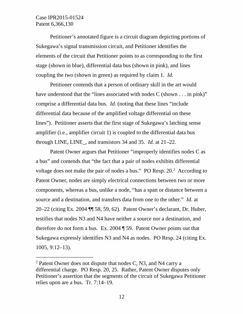
Petitioner’s annotated figure is a circuit diagram depicting portions of
Sukegawa’s signal transmission circuit, and Petitioner identifies the
elements of the circuit that Petitioner points to as corresponding to the first
stage (shown in blue), differential data bus (shown in pink), and lines
coupling the two (shown in green) as required by claim 1. Id.
Petitioner contends that a person of ordinary skill in the art would
have understood that the “lines associated with nodes C (shown . . . in pink)”
comprise a differential data bus. Id. (noting that these lines “include
differential data because of the amplified voltage differential on these
lines”). Petitioner asserts that the first stage of Sukegawa’s latching sense
amplifier (i.e., amplifier circuit 1) is coupled to the differential data bus
through LINE, LINE_, and transistors 34 and 35. Id. at 21–22.
Patent Owner argues that Petitioner “improperly identifies nodes C as
a bus” and contends that “the fact that a pair of nodes exhibits differential
voltage does not make the pair of nodes a bus.” PO Resp. 20.2 According to
Patent Owner, nodes are simply electrical connections between two or more
components, whereas a bus, unlike a node, “has a span or distance between a
source and a destination, and transfers data from one to the other.” Id. at
20–22 (citing Ex. 2004 ¶¶ 58, 59, 62). Patent Owner’s declarant, Dr. Huber,
testifies that nodes N3 and N4 have neither a source nor a destination, and
therefore do not form a bus. Ex. 2004 ¶ 59. Patent Owner points out that
Sukegawa expressly identifies N3 and N4 as nodes. PO Resp. 24 (citing Ex.
1005, 9:12–13).
2 Patent Owner does not dispute that nodes C, N3, and N4 carry a differential charge. PO Resp. 20, 25. Rather, Patent Owner disputes only Petitioner’s assertion that the segments of the circuit of Sukegawa Petitioner relies upon are a bus. Tr. 7:14–19.
Case IPR2015-01524 Patent 6,366,130
13
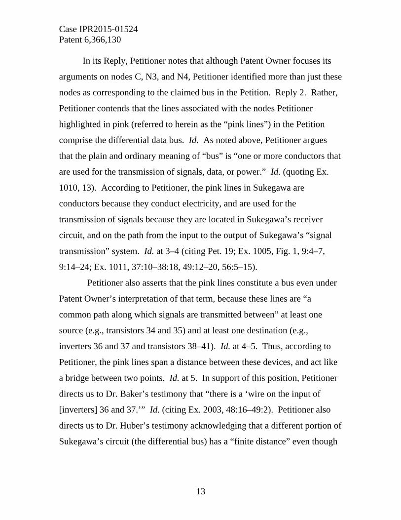
In its Reply, Petitioner notes that although Patent Owner focuses its
arguments on nodes C, N3, and N4, Petitioner identified more than just these
nodes as corresponding to the claimed bus in the Petition. Reply 2. Rather,
Petitioner contends that the lines associated with the nodes Petitioner
highlighted in pink (referred to herein as the “pink lines”) in the Petition
comprise the differential data bus. Id. As noted above, Petitioner argues
that the plain and ordinary meaning of “bus” is “one or more conductors that
are used for the transmission of signals, data, or power.” Id. (quoting Ex.
1010, 13). According to Petitioner, the pink lines in Sukegawa are
conductors because they conduct electricity, and are used for the
transmission of signals because they are located in Sukegawa’s receiver
circuit, and on the path from the input to the output of Sukegawa’s “signal
transmission” system. Id. at 3–4 (citing Pet. 19; Ex. 1005, Fig. 1, 9:4–7,
9:14–24; Ex. 1011, 37:10–38:18, 49:12–20, 56:5–15).
Petitioner also asserts that the pink lines constitute a bus even under
Patent Owner’s interpretation of that term, because these lines are “a
common path along which signals are transmitted between” at least one
source (e.g., transistors 34 and 35) and at least one destination (e.g.,
inverters 36 and 37 and transistors 38–41). Id. at 4–5. Thus, according to
Petitioner, the pink lines span a distance between these devices, and act like
a bridge between two points. Id. at 5. In support of this position, Petitioner
directs us to Dr. Baker’s testimony that “there is a ‘wire on the input of
[inverters] 36 and 37.’” Id. (citing Ex. 2003, 48:16–49:2). Petitioner also
directs us to Dr. Huber’s testimony acknowledging that a different portion of
Sukegawa’s circuit (the differential bus) has a “finite distance” even though
Case IPR2015-01524 Patent 6,366,130
14
Sukegawa does not expressly disclose any physical dimensions. Id. (citing
Ex. 1011, 39:9–23).
Finally, Petitioner argues that the fact that the pink lines in Sukegawa
include nodes does not preclude them from being a bus or detract from other
evidence showing that Sukegawa discloses a differential data bus. Id. at 6.
ii. Analysis
For the reasons discussed below, based on the evidence developed
during trial, we find that Sukegawa discloses a differential data bus.
As discussed above, we determine that the broadest reasonable
interpretation of “bus” in light of the ’130 patent Specification is “one or
more conductors that are used for the transmission of signals, data, or
power.” Ex. 1010, 13; Reply 2. Sukegawa discloses a “signal transmission
circuit,” wherein a signal is transmitted to receiver circuit 4 containing
output terminals OUT and OUT_. Ex. 1005, Fig. 1, 9:4–24. We agree with
Petitioner that the lines between transistor 34 and inverter 36 are used to
transmit signals from input 4a to the output labeled OUT_, and that the lines
between transistor 35 and inverter 37 are used to transmit signals from input
4b to the output labeled OUT. Pet. 23–25; Reply 3–5; Ex. 1005, Fig. 1, 9:4–
7, 9:14–24; Ex. 1011, 37:10–38:18. Sukegawa explains that these lines
carry a voltage (i.e., an electrical signal). Ex. 1005, 8:59–64, 9:4–7; Pet. 26;
Ex. 1002 ¶ 31. Dr. Huber, Patent Owner’s declarant, agreed that “the
connections of the various transistors” in Sukegawa Figure 1, including
transistors 34 and 35, are conductors. Ex. 1011, 48:25–49:20. We agree
with Petitioner that a person of ordinary skill in the art would consider these
lines to be conductors. Reply 3. Thus, under our (and Petitioner’s)
Case IPR2015-01524 Patent 6,366,130
15
construction of the term “bus,” the pink lines Petitioner identified in
Sukegawa comprise a “bus.”
Patent Owner does not dispute expressly that Sukegawa discloses a
differential data bus according to Petitioner’s understanding of the plain and
ordinary meaning of “bus,” which we adopt. Instead, Patent Owner
proposes that Petitioner’s proposed meaning is incorrect. Tr. 34:14–17. For
the reasons discussed above, we disagree.
Nevertheless, we agree with Petitioner that Sukegawa discloses a bus
even under Patent Owner’s understanding of the term. Reply 4–5. For
example, the pink lines in Sukegawa comprise a path along which
transmission signals travel from transistors 34 and 35 (i.e., sources) to
inverters 36 and 37, on their way to outputs OUT_ and OUT, respectively
(i.e., destinations). Ex. 1005, Fig. 1; 8:59–64, 9:4–7.
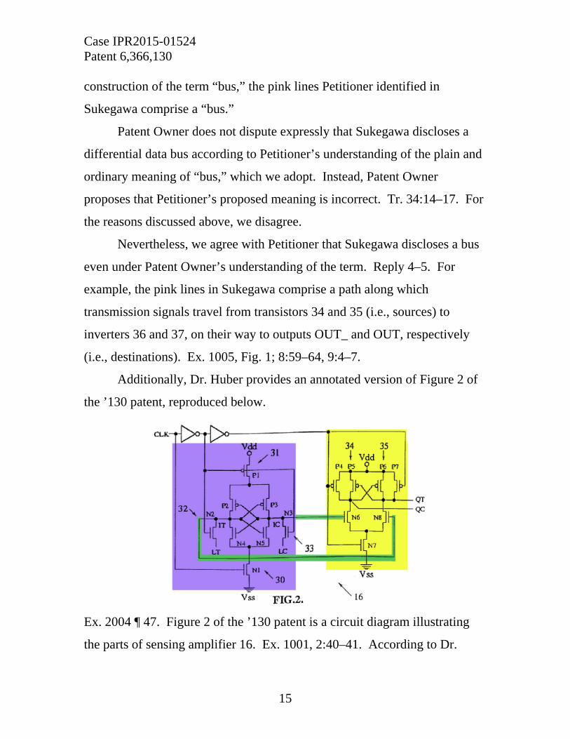
Additionally, Dr. Huber provides an annotated version of Figure 2 of
the ’130 patent, reproduced below.
Ex. 2004 ¶ 47. Figure 2 of the ’130 patent is a circuit diagram illustrating
the parts of sensing amplifier 16. Ex. 1001, 2:40–41. According to Dr.
Case IPR2015-01524 Patent 6,366,130
16
Huber, the portions highlighted in green comprise a “differential data bus.”
Ex. 2004 ¶ 47.
The only apparent difference between the green lines in Figure 2 of
the ’130 patent and the pink lines in Sukegawa is the length of the lines. Tr.
35:21–36:2. Although Patent Owner contends a bus needs to span some
distance, neither Patent Owner nor Dr. Huber set forth a specific distance
requirement for something to be a bus. Instead, when referring to LINE and
LINE_ in Figure 1 of Sukegawa, which Dr. Huber admitted comprise a bus,
Dr. Huber testified that “I think it’s clear from the drawing that it is a -- a
finite distance. It’s not a zero distance or it’s not a distance that you can
minimize. It looks to be transmitting from one portion of the circuit to
another portion, which are physically separate.” Ex. 1011, 39:13–23.
Figure 1 of Sukegawa likewise shows a finite, non-zero distance
between transistors 34 and 35 and inverters 36 and 37, respectively, and
discloses transmitting from one portion of the circuit to another portion.
Although Dr. Baker testified that a person of ordinary skill in the art would
seek to minimize the distance between node and inverter, he maintained that
there would be a wire there. Ex. 2003, 47:19–49:2. We agree.
In contesting that Sukegawa discloses a differential data bus under its
interpretation, Patent Owner focuses on nodes C, N3, and N4, arguing that
these components do not constitute a bus. Petitioner, however, relies on
more than just nodes C, N3, and N4 as corresponding to the bus.
Additionally, Dr. Baker testified that “a bus may have multiple wires with
multiple nodes.” Ex. 2003, 57:5–6. This appears to be consistent not only
with what the green lines of the ’130 patent depict, which Dr. Huber testified
comprise a bus, but also with what the pink lines in Sukegawa depict. Patent
Case IPR2015-01524 Patent 6,366,130
17
Owner’s argument, therefore, is unavailing, as it fails to address directly and
adequately Petitioner’s assertion that the pink lines associated with nodes C,
N3, and N4, and not just the nodes themselves, comprise the differential data
bus.
Based on the foregoing, we find that Petitioner has established by a
preponderance of the evidence that the pink lines in Sukegawa constitute a
differential data bus under either party’s meaning of the term.
iii. “precharge to a voltage Vpr between Vdd and ground”
Claim 1 additionally requires that the differential bus and differential
data bus are precharged “to a voltage Vpr between Vdd and ground.”
Petitioner contends that the differential bus in Sukegawa is precharged to an
intermediate voltage Vdd/2 (i.e., a voltage between Vdd and ground). Pet.
25. Petitioner acknowledges Sukegawa discloses that the differential data
bus is precharged to Vdd, but notes that Sukegawa “provides no criticism of
precharging the ‘differential data bus’ to a value under Vdd, such as Vdd/2.”
Reply 8. Petitioner contends that given the advantages of precharging to an
intermediate voltage, for example, as taught by Lu, a person of ordinary skill
in the art would have had reason to modify Sukegawa in view of Lu, and
precharge the differential data bus to Vdd/2 instead of Vdd. Pet. 26–27;
Reply 7–8. Specifically, Petitioner argues that
[o]ne of ordinary skill in the art . . . would have understood that precharging to an intermediate voltage would have been desirable to speed up operation of the circuit because pulling up or pulling down a node precharged to an intermediate voltage to full logic levels would require a smaller voltage swing (and thus be faster) versus a full Vdd voltage swing to pull down a node precharged to Vdd (as disclosed in Sukegawa with respect to the differential data bus).
Case IPR2015-01524 Patent 6,366,130
18
Pet. 26–27 (citing Lu’s teaching that “[a]t sensing and bit-line precharge in
half-VDD sensing, the pullup and pulldown of bitlines are balanced and have
only half-VDD swing”); Reply 7; Ex. 1002 ¶ 31. Petitioner contends that the
advantages of intermediate voltage precharging were well-known in the art,
as acknowledged by Dr. Huber and as set forth explicitly in Lu. Pet. 26–27;
Reply 7, 11; Ex. 1008, Abstract, 453 (listing advantages (1)–(4) of
intermediate voltage precharging); Ex. 1011, 58:15–59:18; Ex. 1002 ¶ 31.
Petitioner also contends that applying the teachings of Lu to
Sukegawa “would have amounted to nothing more than the use of a known
technique to improve similar devices in the same way and would have
yielded nothing more than predictable results.” Pet. 27 (citing KSR, 550
U.S. at 417); Reply 11–12. In support of its position, Petitioner directs us to
Dr. Baker’s testimony explaining that a person of ordinary skill in the art
would have been able to make the necessary adjustments to Sukegawa so
that it would work. Reply 12–14 (citing Ex. 1002 ¶ 31; Ex. 2003, 63:20–
64:1, 64:7–12, 75:9–16, 79:15–81:23, 109:23–110:8).
Patent Owner argues that Sukegawa teaches away from precharging
the differential data bus to Vdd/2 because it explicitly teaches precharging
that bus to Vdd. PO Resp. 28–30. According to Patent Owner,
[s]ince Sukegawa knew and practiced Vdd/2 in the same invention and specifically chose not to bring nodes N3 and N4 to Vdd/2, but rather to Vdd, this leads the person of ordinary skill in the art in a divergent direction by teaching that it would be undesirable to bring nodes N3 and N4 to some intermediate value, but rather that they should be brought completely to Vdd.
Id. at 29–30; Ex. 2004 ¶¶ 65–66.
Patent Owner also argues that Petitioner’s proposed modification to
precharge nodes N3 and N4 to Vdd/2 would result in “an unacceptable and
Case IPR2015-01524 Patent 6,366,130
19
practically unworkable circuit with undesirable leakage currents.” PO Resp.
33–34. In support of its position, Patent Owner directs us to testimony from
Dr. Huber who concludes that modifying Sukegawa in view of Lu, as
suggested by Dr. Baker, would result in unacceptable “power-wasting
current paths.” Ex. 2004 ¶¶ 67–71; PO Resp. 30–34.
Patent Owner additionally argues that Lu fails to disclose or suggest
precharging to Vdd/2. PO Resp. 34. Patent Owner asserts that Lu does not
define any definite precharging value, but instead teaches precharging two
bit-line halves at “nearly half VDD,” which means that the bit-line halves are
floating, and their voltages can change over time. Id. at 35–36 (citing Ex.
1008, 452; Ex. 2004 ¶ 74; Ex. 2003, 26:18–27:4, 28:10–17). According to
Patent Owner, claim 1 requires a precharge voltage that does not float. Id. at
37.
iv. Analysis
For the reasons discussed below, based on the evidence developed
during trial, we find that the combined teachings of Sukegawa and Lu
disclose precharging the differential data bus to a voltage between Vdd and
ground, and that a person of ordinary skill in the art would have been
motivated to combine the references’ teachings.
Sukegawa and Lu each disclose precharging certain portions of a
circuit to Vdd/2. Ex. 1005, 7:29–31 (“In this case, the voltage at nodes 101
and 102 becomes the intermediate voltage VDD/2 . . . .”); Ex. 1008, Abstract
(“A sensing scheme in which the bit line is precharged to half VDD is
introduced from CMOS DRAM’s.”). Contrary to Patent Owner’s argument
that Lu fails to disclose a precharging source, Lu expressly states that “[t]he
bit lines are precharged to a reference voltage approximately equal to VDD/2,
Case IPR2015-01524 Patent 6,366,130
20
which can be obtained from a voltage regulator.” Ex. 1008, 451. Lu
describes this as one of two possible mechanisms for precharging to Vdd/2,
the other mechanism involving shorting two bit-line halves. Id. In arguing
that Lu fails to disclose any definite precharging value, Patent Owner
focuses on Lu’s disclosure of the operation involving shorting two bit-line
halves, and does not address the alternative mechanism. PO Resp. 34–35.
Thus, even if we were to agree with Patent Owner’s argument with regard to
the shorting mechanism, this would not detract from Lu’s disclosure of the
alternative mechanism for precharging to Vdd/2 using a voltage regulator.
See In re Fritch, 972 F.2d 1260, 1264 (Fed. Cir. 1992) (“It is well settled
that a prior art reference is relevant for all that it teaches to those of ordinary
skill in the art.”).
We recognize that Sukegawa teaches pre-charging the differential data
bus to Vdd, not Vdd/2. Lu, however, expressly discloses several advantages
of pre-charging to Vdd/2, including increasing chip reliability, providing
better speed, and reducing power for charging and discharging the bit lines.
Ex. 1008, 453. Dr. Huber likewise testified that there are “many
advantages” to intermediate voltage precharging. Ex. 1011, 58:15–59:15.
Petitioner has thus provided evidence demonstrating a reason, based on a
rational underpinning, that a person of ordinary skill in the art would apply
the teachings of Lu to Sukegawa, and precharge the differential data bus of
Sukegawa to Vdd/2. In re Kahn, 441 F.3d 977, 988 (Fed. Cir. 2006).
As to Patent Owner’s contention that Sukegawa teaches away from
precharging the differential data bus to Vdd/2, the Federal Circuit has stated
that
Case IPR2015-01524 Patent 6,366,130
21
[a] reference may be said to teach away when a person of ordinary skill, upon reading the reference, would be discouraged from following the path set out in the reference, or would be led in a direction divergent from the path that was taken by the applicant. The degree of teaching away will of course depend on the particular facts; in general, a reference will teach away if it suggests that the line of development flowing from the reference’s disclosure is unlikely to be productive of the result sought by the applicant.
In re Gurley, 27 F.3d 551, 553 (Fed. Cir. 1994).
Patent Owner’s teaching away argument is primarily based on the fact
that Sukegawa “specifically chose not to bring nodes N3 and N4 to Vdd/2,
but rather to Vdd.” PO Resp. 29. We disagree that Sukegawa’s disclosure
of charging the differential data bus to Vdd, on its own, would lead one of
ordinary skill in the art “in a direction divergent from” implementing a
precharge voltage of Vdd/2, i.e., the path that was taken by the inventor of
the ’130 patent (and Lu). Moreover, Patent Owner does not direct us to
anything in Sukegawa that can be said to discourage a person of ordinary
skill in the art from pre-charging to Vdd/2. To the contrary, the record is
replete with evidence demonstrating the advantages of precharging to a
value below Vdd, as set forth in Lu, and those advantages would apply
equally in the context of precharging the differential data bus. E.g., Ex.
1008, 451, 453. In view of the aforementioned advantages, and the lack of
any evidence of criticism of precharging to Vdd, we find Patent Owner’s
teaching away argument to be unpersuasive. In re Kahn, 441 F.3d at 990;
see also In re Urbanski, 809 F.3d 1237, 1244 (Fed. Cir. 2016) (“Although
Gross generally discloses a relatively longer reaction time that results in
fiber capable of forming stable dispersions, Gross does not criticize or
discredit the use of a shorter reaction time.”)
Case IPR2015-01524 Patent 6,366,130
22
We also disagree with Patent Owner’s contention that modifying
Sukegawa’s circuit in view of Lu’s teachings would result in an
“unacceptable and practically unworkable circuit with undesirable leakage
currents.” PO Resp. 30–34. We have considered Dr. Huber’s testimony that
modifying Sukegawa in view of Lu may lead to “power-wasting current
paths.” Ex. 2004 ¶ 70. We, however, agree with Petitioner’s argument that
this would happen only if the modified Sukegawa system was designed
poorly. Reply 12. We credit Dr. Baker’s testimony that a person of ordinary
skill in the art would have been able to make “simple adjustments to
precharge the bus to Vdd over two” so that “the circuit worked and didn’t
fail.” Ex. 2003, 79:15–81:23; Reply 12–14; see also KSR, 550 U.S. at 418
(“[A] court can take account of the inferences and creative steps that a
person of ordinary skill in the art would employ.”).
For all of the foregoing reasons, we find that Petitioner has
established, by a preponderance of evidence, that the combined teachings of
Sukegawa and Lu disclose precharging the differential data bus to a voltage
between Vdd and ground, as required in claim 1, and that a person of
ordinary skill in the art would have been motivated to combine their
teachings in the manner proposed by Petitioner.
b. The Undisputed Limitations of Claim 1, 2, 6, and 9
Based on the complete record developed during trial, we find that
Petitioner has presented sufficient evidence showing that Sukegawa and Lu
disclose each of the remaining, undisputed limitations of claim 1. For
example, independent claim 1 requires a data transfer arrangement
comprising two bus drivers, a voltage precharge source, and a differential
bus coupled to the bus drivers and to the voltage precharge source.
Case IPR2015-01524 Patent 6,366,130
23
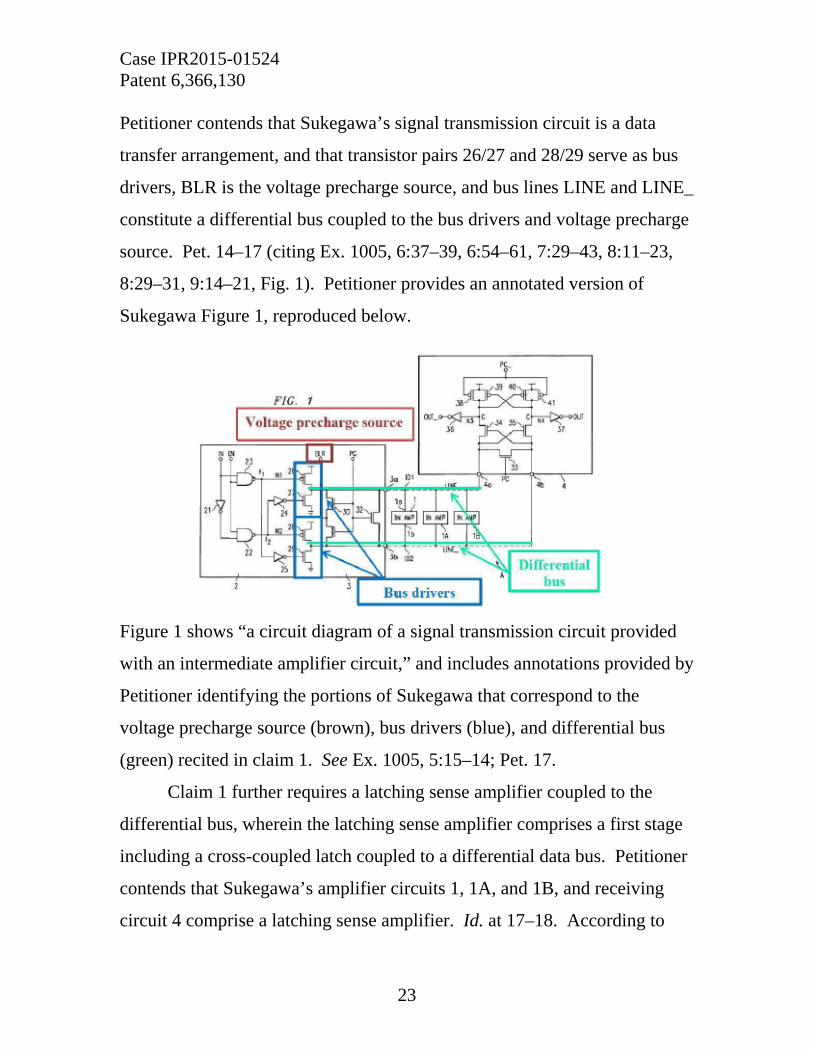
Petitioner contends that Sukegawa’s signal transmission circuit is a data
transfer arrangement, and that transistor pairs 26/27 and 28/29 serve as bus
drivers, BLR is the voltage precharge source, and bus lines LINE and LINE_
constitute a differential bus coupled to the bus drivers and voltage precharge
source. Pet. 14–17 (citing Ex. 1005, 6:37–39, 6:54–61, 7:29–43, 8:11–23,
8:29–31, 9:14–21, Fig. 1). Petitioner provides an annotated version of
Sukegawa Figure 1, reproduced below.
Figure 1 shows “a circuit diagram of a signal transmission circuit provided
with an intermediate amplifier circuit,” and includes annotations provided by
Petitioner identifying the portions of Sukegawa that correspond to the
voltage precharge source (brown), bus drivers (blue), and differential bus
(green) recited in claim 1. See Ex. 1005, 5:15–14; Pet. 17.
Claim 1 further requires a latching sense amplifier coupled to the
differential bus, wherein the latching sense amplifier comprises a first stage
including a cross-coupled latch coupled to a differential data bus. Petitioner
contends that Sukegawa’s amplifier circuits 1, 1A, and 1B, and receiving
circuit 4 comprise a latching sense amplifier. Id. at 17–18. According to
Case IPR2015-01524 Patent 6,366,130
24
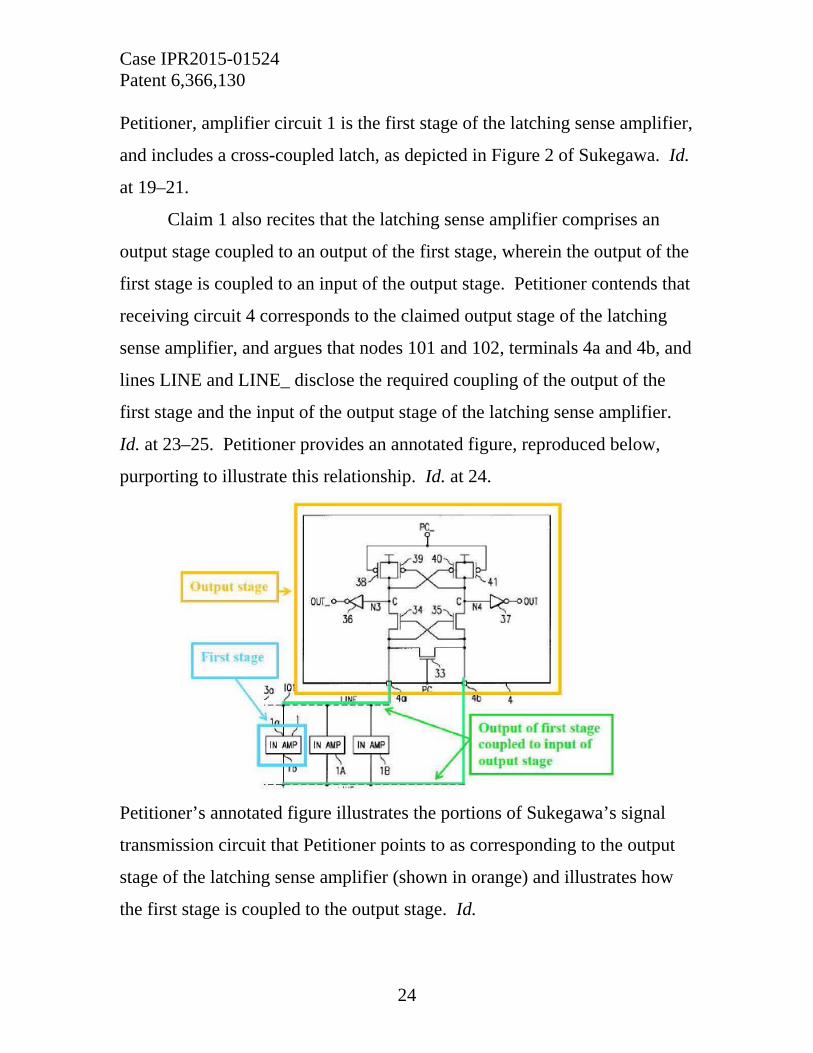
Petitioner, amplifier circuit 1 is the first stage of the latching sense amplifier,
and includes a cross-coupled latch, as depicted in Figure 2 of Sukegawa. Id.
at 19–21.
Claim 1 also recites that the latching sense amplifier comprises an
output stage coupled to an output of the first stage, wherein the output of the
first stage is coupled to an input of the output stage. Petitioner contends that
receiving circuit 4 corresponds to the claimed output stage of the latching
sense amplifier, and argues that nodes 101 and 102, terminals 4a and 4b, and
lines LINE and LINE_ disclose the required coupling of the output of the
first stage and the input of the output stage of the latching sense amplifier.
Id. at 23–25. Petitioner provides an annotated figure, reproduced below,
purporting to illustrate this relationship. Id. at 24.
Petitioner’s annotated figure illustrates the portions of Sukegawa’s signal
transmission circuit that Petitioner points to as corresponding to the output
stage of the latching sense amplifier (shown in orange) and illustrates how
the first stage is coupled to the output stage. Id.
Case IPR2015-01524 Patent 6,366,130
25
We have also reviewed Petitioner’s arguments and evidence for
claims 2, 6, and 9 (id. at 27–33) and find that Petitioner has met its burden of
establishing that Sukegawa and Lu disclose or suggest all of the limitations
of those claims as well.
c. The Disputed Limitation of Claim 5
Claim 5 depends from claim 1, and further requires that “the voltage
precharge source is configured to precharge the differential bus to a
predetermined voltage that is less than a logic high voltage and greater than
a logic low voltage.”
Petitioner contends that Sukegawa discloses precharging the
differential bus LINE and LINE_ to Vdd/2, which is a voltage less than a
logic high and greater than a logic low. Pet. 29 (citing Ex. 1005 7:26–37,
8:28–31, 9:14–21; Ex. 1002 ¶ 33).
Patent Owner contends that Dr. Baker does not mention the terms
“logic high voltage” or “logic low voltage” in his declaration, and explains
that the logic high voltage must be less than Vdd, and the logic low voltage
must be greater than ground. PO Resp. 38–41. Dr. Huber provides a figure,
reproduced below, to aid in understanding this relationship.
Case IPR2015-01524 Patent 6,366,130
26
Ex. 2004 ¶ 92. This figure from Dr. Huber’s declaration shows an alleged
relationship between Vdd, Vdd/2, ground, logic high voltage, and logic low
voltage. PO Resp. 41. Patent Owner contends that Petitioner fails to show
that Sukegawa and Lu disclose or suggest a precharge voltage less than a
logic high voltage and greater than a logic low voltage. Id. at 42.
We disagree. It is undisputed that Sukegawa discloses precharging
the differential bus to a value of Vdd/2. Ex. 1005, 7:26–37; Pet. 25–26; PO
Resp. 28–29. According to Patent Owner’s own information and arguments,
including Dr. Huber’s figure reproduced above, a precharge value of Vdd/2
is lower than a logic high voltage and greater than a logic low voltage. PO
Resp. 41–42; Ex. 2004 ¶ 92. We, therefore, agree with Petitioner that
Sukegawa discloses precharging a differential bus to a value less than a logic
high voltage and greater than a logic low value. See Reply 16–17.
d. Hindsight
Patent Owner argues that Petitioner “uses impermissible hindsight
reasoning in building its case of obviousness using Sukegawa and Lu.” PO
Case IPR2015-01524 Patent 6,366,130
27
Resp. 43–45. Specifically, Patent Owner contends that Dr. Baker used claim
1 to “cherry pick” each limitation of claim 1 from the prior art references.
Id. at 43–44 (citing Ex. 2003, 24:18–26:5). We disagree. As discussed
above, Petitioner has demonstrated where each reference of the prior art
discloses or suggests each limitation of claim 1, and has directed us to
evidence from within those references establishing that a person of ordinary
skill in the art would have had reason to combine the teachings of the prior
art references to arrive at the claimed invention. Thus, contrary to Patent
Owner’s contention, the preponderance of the evidence suggests that
Petitioner’s combination of prior art references is based on the references
themselves, and not based on using the ’130 patent disclosure as a guide.
e. Conclusion
For all of the foregoing reasons, having considered the parties’
contentions and supporting evidence developed during the trial, we
determine that Petitioner has demonstrated by a preponderance of the
evidence that claims 1, 2, 5, 6, and 9 are unpatentable under 35 U.S.C. § 103
over the combined teachings of Sukegawa and Lu.
2. Claim 3
Petitioner contends that the subject matter of claim 3 would have been
obvious over Sukegawa, Lu, and Watanabe. Pet. 33–45.
Claim 3 depends from claim 1, and further requires that the first stage
of the latching sense amplifier comprises a plurality of input pass transistors
and a plurality of NMOS and PMOS transistors, with each having a gate, a
source, and a drain. Claim 3 additionally specifies how the drains, gates,
and sources of the transistors are coupled to one another and/or to a clock
signal:
Case IPR2015-01524 Patent 6,366,130
28
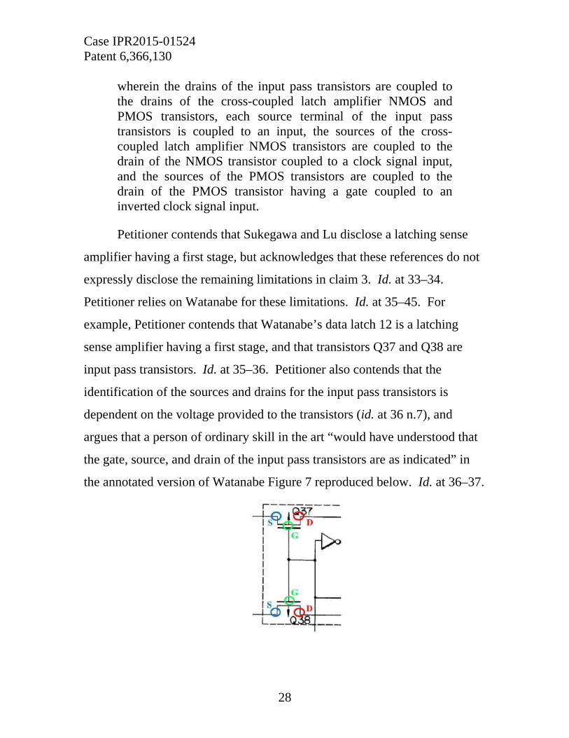
wherein the drains of the input pass transistors are coupled to the drains of the cross-coupled latch amplifier NMOS and PMOS transistors, each source terminal of the input pass transistors is coupled to an input, the sources of the cross-coupled latch amplifier NMOS transistors are coupled to the drain of the NMOS transistor coupled to a clock signal input, and the sources of the PMOS transistors are coupled to the drain of the PMOS transistor having a gate coupled to an inverted clock signal input.
Petitioner contends that Sukegawa and Lu disclose a latching sense
amplifier having a first stage, but acknowledges that these references do not
expressly disclose the remaining limitations in claim 3. Id. at 33–34.
Petitioner relies on Watanabe for these limitations. Id. at 35–45. For
example, Petitioner contends that Watanabe’s data latch 12 is a latching
sense amplifier having a first stage, and that transistors Q37 and Q38 are
input pass transistors. Id. at 35–36. Petitioner also contends that the
identification of the sources and drains for the input pass transistors is
dependent on the voltage provided to the transistors (id. at 36 n.7), and
argues that a person of ordinary skill in the art “would have understood that
the gate, source, and drain of the input pass transistors are as indicated” in
the annotated version of Watanabe Figure 7 reproduced below. Id. at 36–37.
Case IPR2015-01524 Patent 6,366,130
29
Petitioner’s annotated figure illustrates the portions of Watanabe Figure 7
that Petitioner points to as corresponding to the gate, source, and drain of the
input pass transistors Q37 and Q38.
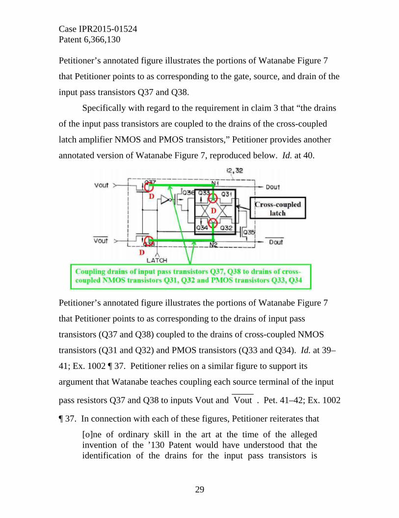
Specifically with regard to the requirement in claim 3 that “the drains
of the input pass transistors are coupled to the drains of the cross-coupled
latch amplifier NMOS and PMOS transistors,” Petitioner provides another
annotated version of Watanabe Figure 7, reproduced below. Id. at 40.
Petitioner’s annotated figure illustrates the portions of Watanabe Figure 7
that Petitioner points to as corresponding to the drains of input pass
transistors (Q37 and Q38) coupled to the drains of cross-coupled NMOS
transistors (Q31 and Q32) and PMOS transistors (Q33 and Q34). Id. at 39–
41; Ex. 1002 ¶ 37. Petitioner relies on a similar figure to support its
argument that Watanabe teaches coupling each source terminal of the input
pass resistors Q37 and Q38 to inputs Vout and Vout . Pet. 41–42; Ex. 1002
¶ 37. In connection with each of these figures, Petitioner reiterates that
[o]ne of ordinary skill in the art at the time of the alleged invention of the ’130 Patent would have understood that the identification of the drains for the input pass transistors is
Case IPR2015-01524 Patent 6,366,130
30
dependent on the voltage provided to the transistors from vout
and vout . Nonetheless, the identification of the drains in
annotated Fig. 7 of Watanabe is consistent with the ’130 Patent’s specification and identification of drains for the claimed input pass transistors. See, e.g., Ex. 1002, ¶ 37, n.2.
Pet. 40 n.8; see also id. at 41 n.9 (with respect to the identification of
sources).
Petitioner asserts that it would have been obvious to a person of
ordinary skill in the art to modify Sukegawa and Lu in view of Watanabe
because the first stage of Watanabe’s latching sense amplifier provides
certain advantages, such as increased speed and a smaller circuit layout. Id.
at 34. Petitioner also contends that modifying Sukegawa’s first stage with
Watanabe’s first stage would have amounted to using a known technique to
improve similar devices in the same way, yielding predictable results. Id.
(citing KSR, 550 U.S. at 417).
Patent Owner argues that the combination of Sukegawa, Lu, and
Watanabe fails to disclose all of the elements of claim 3, specifically
“wherein the drains of the input pass transistors are coupled to the drains of
the cross-coupled latch amplifier NMOS and PMOS transistors [and] each
source terminal of the input pass transistors is coupled to an input.” PO
Resp. 47–48. Patent Owner agrees that “the identification of the sources and
drains for the input pass transistors is dependent on the voltage provided to
the transistors.” Id. at 48 (quoting Pet. 36–37 n.7). Patent Owner, however,
contends that the input pass transistors in Watanabe are PMOS transistors,
whereas the input pass transistors in the ’130 patent Specification are NMOS
transistors, and asserts that the designations of source and drain are opposite
for NMOS and PMOS transistors. Id. at 48–49; Ex. 2004 ¶ 82, 84 (stating
Case IPR2015-01524 Patent 6,366,130
31
that “for any given set of voltages in a circuit, the drain of an NMOS
transistor corresponds to the source of a PMOS transistor”). According to
Dr. Huber, substituting the PMOS input pass transistors of Watanabe for the
NMOS input pass transistors of the ’130 patent would lead to the sources of
the input pass transistor being coupled with the drains of the cross-coupled
latch amplifier, which is the opposite of what is required in claim 3. Ex.
2004 ¶ 85.
a. Analysis
The parties agree that the identification of sources and drains for the
input pass transistors of Watanabe depends upon the voltage applied to the
circuit from Vout and Vout . Pet. 36–37 n.7; PO Resp. 48. Based on this,
Petitioner argues that the transistors of Watanabe’s circuit would be
configured with sources and drains as shown in Petitioner’s annotated
figures (reproduced above) in at least one instance during the operation of
the circuit as certain voltages are applied across the transistors. Tr. 18:5–10,
42:11–18; Ex. 1002 ¶ 37. We, however, are not persuaded that simply
understanding the relationship between the applied voltage and the
identification of sources and drains of a transistor, on its own, is sufficient to
establish that the prior art discloses or suggests the specific limitations
directed to the configuration and coupling of sources and drains of the
various transistors recited in claim 3. See Lindemann Maschinenfabrik
GMBH v. American Hoist & Derrick Co., 730 F.2d 1452, 1462 (Fed. Cir.
1984) (“That the claimed invention may employ known principles does not
in itself establish that the invention would have been obvious.”).
For example, Petitioner does not dispute that Watanabe’s input pass
transistors are PMOS transistors. Tr. 19:23–25. Additionally, neither
Case IPR2015-01524 Patent 6,366,130
32
Petitioner nor Dr. Baker contests Dr. Huber’s testimony that “[f]or a PMOS
transistor, the drain is identified as the terminal (considering the source and
drain) with the more negative (or less positive) voltage.” Ex. 2004 ¶ 82.
Petitioner, however, fails to direct us to evidence in Watanabe or elsewhere
indicating the value of the voltages at the various terminals of Watanabe’s
input pass transistors. Although Dr. Baker cites to various portions of
Watanabe throughout his declaration to support his testimony that Q37 and
Q38 are input pass transistors, Dr. Baker does not explain how those
portions of Watanabe would allow a person of ordinary skill in the art to
identify the sources and drains of the input pass transistors, or their
relationship to the terminals of the other transistors in the circuit, as required
by claim 3. Ex. 1002 ¶ 37; Pet. 36–42.
Moreover, we are not persuaded by Petitioner’s contention that its
identification of the sources and drains in annotated Figure 7 of Watanabe is
consistent with the identification of sources and drains in the ’130 patent
Specification. Pet. 36–37 n. 7. Not only does Petitioner fail to provide any
information supporting that assertion, but, as Patent Owner points out, the
input pass transistors in the ’130 patent (N2 and N3) are NMOS devices,
whereas the input pass transistors in Watanabe (Q37 and Q38) are PMOS
devices. It is undisputed that the designations of source and drain are
opposite for NMOS and PMOS transistors. PO Resp. 48; Ex. 2004 ¶ 82.
This evidence suggests that upon being exposed to the same voltage, the
designation of sources and drains for the input pass transistors in Watanabe
would be opposite of the designations of sources and drains for the input
pass transistors of the ’130 patent.
Case IPR2015-01524 Patent 6,366,130
33
Nor are we persuaded by Petitioner’s assertion that Patent Owner’s
arguments are based on “an unreasonable narrow interpretation of ‘coupled’
to mean ‘directly connected.’” Reply 19. In arguing that Patent Owner’s
narrow interpretation is flawed, Petitioner states that “[b]ecause the voltages
appearing on the pass transistor terminals change during the ’130 preferred
embodiment operation, a pass transistor terminal is considered to be a
‘source’ at certain times, and a ‘drain’ at other times,” and provides an
analysis of voltages flowing throughout a circuit of the ’130 patent during a
preferred embodiment operation. Id. at 20–21. As noted above, however,
Petitioner fails to provide a similar analysis of the voltages flowing through
the terminals of Watanabe’s input pass transistors or any other transistors
during operation. Accordingly, we find that Petitioner has failed to provide
evidence sufficient to prove, by a preponderance of evidence, that the
terminals of the various transistors and inputs in Watanabe are coupled as
required in claim 3. See 37 C.F.R. § 42.104(b)(4) (stating that “[t]he petition
must specify where each element of the claim is found in the prior art
patents or printed publications relied upon”).
As a result, we find that Petitioner has failed to demonstrate by a
preponderance of evidence that the combined teachings of Sukegawa, Lu,
and Watanabe disclose or suggest all of the limitations of claim 3.
3. Claim 7
Petitioner contends that the subject matter of claim 7 would have been
obvious over Sukegawa, Lu, and Hardee. Pet. 45–47.
Claim 7 ultimately depends from claim 1, and requires active pull up
and active pull down bus drivers that are NMOS transistors. Petitioner
contends that Sukegawa discloses active pull down drivers that are NMOS
Case IPR2015-01524 Patent 6,366,130
34
transistors, but does not expressly disclose active pull up drivers that are
NMOS transistors. Pet. 45. Petitioner thus relies on Hardee for its
disclosure of using NMOS transistors as pull up and pull down drivers. Id.
at 45–46. Petitioner argues that a person of ordinary skill in the art would
have been motivated to modify Sukegawa and Lu to include NMOS pull up
and pull down drivers in view of Hardee “to reduce the layout area and
avoid latch-up.” Id. at 46–47; Ex. 1002 ¶ 41. Specifically, Petitioner
contends that modifying Sukegawa in view of Hardee would result in an
area savings of over 9% in the bus drivers. Reply 22. Petitioner further
contends that “[w]hile ‘[a]voiding latch-up is especially important when
driving signal off-chip,’ . . . latch-up is a concern in CMOS processes aside
from the use of off-chip signals.” Id. at 23 (citing Pet. 47; Ex. 1012, 1).
Additionally, Petitioner argues that using solely NMOS transistors as
bus drivers in Sukegawa and Lu would have been merely a design choice,
and amounted to using a known technique to improve similar devices to
yield predictable results. Pet. 47; Reply 24.
Patent Owner argues that a person of ordinary skill in the art would
not have been motivated to combine the teachings of Hardee with those of
Sukegawa. PO Resp. 53. According to Patent Owner, the alleged
advantages identified by Petitioner are “non-existent.” Id. at 53–55. With
regard to reducing the layout area, Dr. Huber testifies that Sukegawa’s
PMOS transistors constitute a very small portion of Sukegawa’s total
circuitry, and therefore “any area savings from converting [Sukegawa’s]
PMOS transistors 26 and 28 to NMOS would be insignificant.” Ex. 2004
¶ 98; PO Resp. 53. Specifically, Patent Owner calculates the area savings to
be less than 0.8% of the total circuit area. PO Resp. 53–54; Ex. 2004 ¶ 99.
Case IPR2015-01524 Patent 6,366,130
35
Patent Owner also argues that latch-up is not a problem because latch-
up is a “failure mode in transistor circuits that drive external circuits,”
whereas transistors 26 and 28 of Sukegawa “receive their inputs and drive
their outputs to other on-chip components.” PO Resp. 53–54; Ex. 2004 ¶
100. Patent Owner further contends that substituting Hardee’s NMOS pull-
up transistors for Sukegawa’s PMOS pull-down transistors could require
signal boosting, which would add “circuit complexity and consume[]
additional power.” PO Resp. 54–55; Ex. 2004 ¶¶ 101–102.
Upon review of the parties’ contentions and supporting evidence
during trial, we determine that Petitioner has established, by a
preponderance of evidence, that the subject matter of claim 7 would have
been obvious in view of Sukegawa, Lu, and Hardee. We have reviewed
Petitioner’s undisputed explanation of how each claim limitation is taught or
suggested by the combination of prior art references, and find that Petitioner
has met its burden of establishing that Sukegawa, Lu, and Hardee disclose or
suggest all of the limitations of claim 7. Pet. 45–47; Reply 21–24; Ex. 1002
¶¶ 38–42.
We also find Petitioner’s assertion that a person of ordinary skill in
the art would have had reason to combine the teachings of the prior art to
arrive at the claimed subject matter, to be reasonable and supported
adequately by evidence developed during trial. Pet. 45–47; Reply 21–24;
Ex. 1002 ¶¶ 38–42. With regard to reducing the layout area, we agree with
Petitioner that Patent Owner does not dispute that substituting Hardee’s
NMOS pull up transistors for Sukegawa’s PMOS pull up transistors would
result in some area savings. Reply 22. Nor does Patent Owner dispute that
reduction in size, in general, is beneficial. Rather, Patent Owner contends
Case IPR2015-01524 Patent 6,366,130
36
that the substitution would only result in “insignificant” area savings,
namely 0.8% of the total circuit area. PO Resp. 53–54. Thus, whether the
area savings are viewed as being 0.8% of the total circuit area (as Patent
Owner argues) or 9% of the area of the bus drivers (as Petitioner argues), it
is undisputed that modifying Sukegawa in view of Hardee would result in
some reduction in layout size, which, according to Dr. Baker, “can be
important when connecting the drivers up to an array of transistors, as used
in a memory, or driving a parallel data bus where the data signals are laid
out directly adjacent to each other.” Ex. 1002 ¶ 41. Petitioner’s analysis,
supported by the testimony of Dr. Baker, is persuasive.
Furthermore, we are persuaded by Petitioner’s argument regarding
avoiding latch-up. Contrary to Patent Owner’s contention that latch-up
would not be a problem in Sukegawa’s circuits because transistors 26 and 28
do not receive or drive off-chip signals (PO Resp. 54), Petitioner has
provided evidence demonstrating that the problem of latch-up is not limited
to transistor circuits that drive external circuits (Reply 23; Ex. 1012, 1).
We have considered Patent Owner’s argument that replacing
Sukegawa’s PMOS pull up drivers with Hardee’s NMOS “could require
boosting voltages above Vdd.” PO Resp. 55. We, however, agree with
Petitioner that the mere possibility of having to boost voltages above Vdd
does not detract from the aforementioned advantages associated with
modifying Sukegawa in view of Hardee’s teachings. Reply 23–24.
For all of the foregoing reasons, we determine that Petitioner has
demonstrated, by a preponderance of the evidence, that claim 7 is
unpatentable under 35 U.S.C. § 103 over the combined teachings of
Sukegawa, Lu, and Hardee.
Case IPR2015-01524 Patent 6,366,130
37
IV. CONCLUSION
Based on the information presented, we conclude that Petitioner has
shown by a preponderance of evidence that:
(1) Sukegawa and Lu render claims 1, 2, 5, 6, and 9 unpatentable as
obvious; and
(2) Sukegawa, Lu, and Hardee render claim 7 unpatentable as
obvious.
Petitioner, however, has not shown by a preponderance of evidence
that Sukegawa, Lu, and Watanabe render claim 3 unpatentable as obvious.
V. ORDER
For the reasons given, it is hereby
ORDERED that claims 1, 2, 5–7, and 9 have been shown to be
unpatentable;
FURTHER ORDERED that claim 3 has not been shown to be
unpatentable; and
FURTHER ORDERED that, because this is a final decision, parties to
the proceeding seeking judicial review of the decision must comply with the
notice and service requirements of 37 C.F.R. § 90.2.
Case IPR2015-01524 Patent 6,366,130
38
PETITIONER:
Naveen Modi Joseph Palys Joseph Rumpler PAUL HASTINGS LLP [email protected] [email protected] [email protected]
PATENT OWNER:
Clifford H. Kraft [email protected] Joseph N. Hosteny NIRO, HALLER & NIRO [email protected]