Embed Size (px)
Citation preview
Low Power, Programmable Impact Sensor and Recorder
Data Sheet ADIS16240
Rev. C Document Feedback Information furnished by Analog Devices is believed to be accurate and reliable. However, no responsibility is assumed by Analog Devices for its use, nor for any infringements of patents or other rights of third parties that may result from its use. Specifications subject to change without notice. No license is granted by implication or otherwise under any patent or patent rights of Analog Devices. Trademarks and registered trademarks are the property of their respective owners.
One Technology Way, P.O. Box 9106, Norwood, MA 02062-9106, U.S.A. Tel: 781.329.4700 ©2009–2012 Analog Devices, Inc. All rights reserved. Technical Support www.analog.com
FEATURES Digital triple-axis accelerometer, ±19 g Programmable event recorder
Internal and external trigger inputs Automatic event data storage in nonvolatile flash
Low power operation Sleep mode current: 100 µA Continuous sampling current: 1 mA, 1 kSPS
Wake-up and record function External trigger input and SPI trigger command
Peak acceleration sample-and-hold Peak XYZ sum-of-squares output 1600 Hz (X, Y) and 550 Hz (Z) sensor bandwidth Digitally controlled sample rate, up to 4096 SPS Programmable alarms for condition monitoring Programmable digital input/output lines
Data-ready output and alarm indicator output Real-time clock Digitally activated self-test Embedded temperature sensor Programmable power management SPI-compatible serial interface Auxiliary 10-bit ADC input Two analog trigger inputs with programmable threshold Single-supply operation: 2.4 V to 3.6 V >4000 g powered shock survivability
APPLICATIONS Crash or impact detection Condition monitoring of valuable goods Safety, shut-off sensing Impact event recording Security sensing and tamper detection
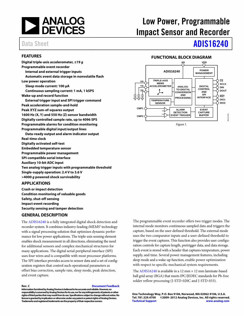
FUNCTIONAL BLOCK DIAGRAM
TRIPLE-AXISMEMS
ACCELEROMETER
TEMPERATURESENSOR
ANALOG-TO-DIGITAL
CONVERSIONAND
PROCESSING
DIGITALCONTROL
ANDSPI
INTERFACE
POWERMANAGEMENT
EVENTCAPTUREBUFFER
ALARMDETECTION
EVENT TRIGGER
CSSCLKDINDOUT
DIO2DIO1RST
VDDAN
XA
YA
ZA
CMP1
ADIS16240
CMP2
0813
3-00
1
Figure 1.
GENERAL DESCRIPTION
The ADIS16240 is a fully integrated digital shock detection and recorder system. It combines industry-leading iMEMS® technology with a signal processing solution that optimizes dynamic perfor-mance for low power applications. The triple-axis sensing element enables shock measurement in all directions, eliminating the need for additional sensors and complex mechanical structures for many applications. The digital serial peripheral interface (SPI) uses four wires and is compatible with most processor platforms. The SPI interface provides access to sensor data and a set of config-uration registers that control such operational parameters as offset bias correction, sample rate, sleep mode, peak detection, and event capture.
The programmable event recorder offers two trigger modes. The internal mode monitors continuous sampled data and triggers the capture, based on the user-defined threshold. The external mode uses the two comparator inputs and a user-defined threshold to trigger the event captures. This function also provides user configu-ration controls for capture length, pretrigger data, and data storage. Each event is stored with a header that captures temperature, power supply, and time. Several power management features, including sleep mode and a wake-up function, enable power optimization with respect to specific mechanical system requirements.
The ADIS16240 is available in a 12 mm × 12 mm laminate-based ball grid array (BGA) that meets IPC/JEDEC standards for Pb-free solder reflow processing (J-STD-020C and J-STD-033).
ADIS16240* PRODUCT PAGE QUICK LINKSLast Content Update: 02/23/2017
COMPARABLE PARTSView a parametric search of comparable parts.
EVALUATION KITS• ADIS16240 Daughter Board
• ADISUSB Evaluation System
DOCUMENTATIONData Sheet
• ADIS16240: Low Power, Programmable Impact Sensor and Recorder Data Sheet
User Guides
• UG-363: ADISUSB User Guide
SOFTWARE AND SYSTEMS REQUIREMENTS• ADIS16240 IIO Programmable Impact Sensor and
Recorder Linux Driver
• ADIS16240 Evaluation Software for the ADISUSB
DESIGN RESOURCES• ADIS16240 Material Declaration
• PCN-PDN Information
• Quality And Reliability
• Symbols and Footprints
DISCUSSIONSView all ADIS16240 EngineerZone Discussions.
SAMPLE AND BUYVisit the product page to see pricing options.
TECHNICAL SUPPORTSubmit a technical question or find your regional support number.
DOCUMENT FEEDBACKSubmit feedback for this data sheet.
This page is dynamically generated by Analog Devices, Inc., and inserted into this data sheet. A dynamic change to the content on this page will not trigger a change to either the revision number or the content of the product data sheet. This dynamic page may be frequently modified.
ADIS16240 Data Sheet
Rev. C | Page 2 of 20
TABLE OF CONTENTS Features .............................................................................................. 1 Applications ....................................................................................... 1 Functional Block Diagram .............................................................. 1 General Description ......................................................................... 1 Revision History ............................................................................... 2 Specifications ..................................................................................... 3
Timing Specifications .................................................................. 4 Absolute Maximum Ratings ............................................................ 5
ESD Caution .................................................................................. 5 Pin Configuration and Function Descriptions ............................. 6 Typical Performance Characteristics ............................................. 7 Theory of Operation ........................................................................ 8
Sensing Element ........................................................................... 8 Data Sampling and Processing ................................................... 8
User Interface .................................................................................8 Capture ...........................................................................................8
Basic Operation .................................................................................9 Memory Map .............................................................................. 10 Output Data Registers................................................................ 11 Event Recorder............................................................................ 12 Operational Control ................................................................... 14
Applications Information .............................................................. 17 Assembly ...................................................................................... 17 Interface Printed Circuit Board (PCB) .................................... 17
Outline Dimensions ....................................................................... 18 Ordering Guide .......................................................................... 18
REVISION HISTORY 12/12—Rev. B to Rev. C
Changes to Features Section............................................................ 1 Removed Bias Voltage Sensitivity from Table 1............................ 3 Changes to Table 7 .......................................................................... 10 Changes to Event Recorder Section ............................................. 12 Added Flash Memory Endurance Management Section .......... 16 Updated Outline Dimensions ....................................................... 18 Changes to Ordering Guide .......................................................... 18
8/12—Rev. A to Rev. B
Updated Outline Dimensions ........................................................ 17
10/11—Rev. 0 to Rev. A
Added Applications Information Section, Figure 23, Figure 24, Figure 25, Renumbered Sequentially ........................................... 16 Updated Outline Dimensions ....................................................... 18 Changes to Ordering Guide .......................................................... 18
4/09—Revision 0: Initial Version
Data Sheet ADIS16240
Rev. C | Page 3 of 20
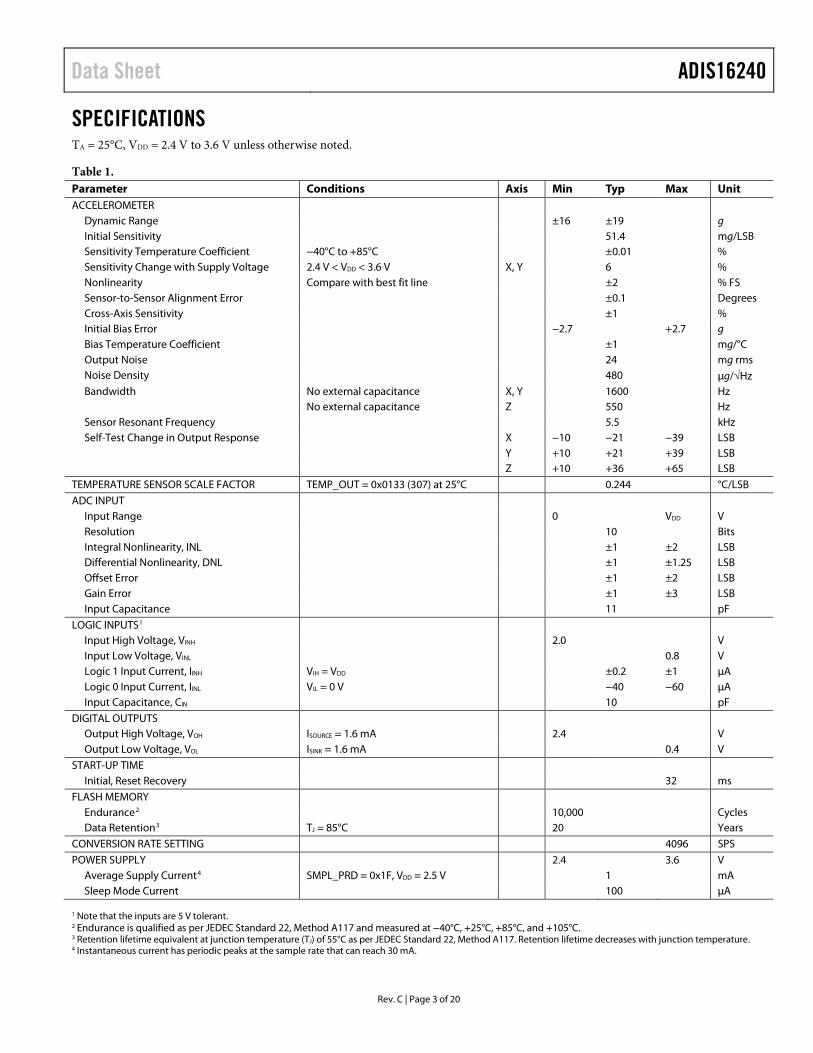
SPECIFICATIONS TA = 25°C, VDD = 2.4 V to 3.6 V unless otherwise noted.
Table 1. Parameter Conditions Axis Min Typ Max Unit ACCELEROMETER
Dynamic Range ±16 ±19 g Initial Sensitivity 51.4 mg/LSB Sensitivity Temperature Coefficient −40°C to +85°C ±0.01 % Sensitivity Change with Supply Voltage 2.4 V < VDD < 3.6 V X, Y 6 % Nonlinearity Compare with best fit line ±2 % FS Sensor-to-Sensor Alignment Error ±0.1 Degrees Cross-Axis Sensitivity ±1 % Initial Bias Error −2.7 +2.7 g Bias Temperature Coefficient ±1 mg/°C Output Noise 24 mg rms Noise Density 480 µg/√Hz Bandwidth No external capacitance X, Y 1600 Hz No external capacitance Z 550 Hz Sensor Resonant Frequency 5.5 kHz Self-Test Change in Output Response X −10 −21 −39 LSB Y +10 +21 +39 LSB Z +10 +36 +65 LSB
TEMPERATURE SENSOR SCALE FACTOR TEMP_OUT = 0x0133 (307) at 25°C 0.244 °C/LSB
ADC INPUT Input Range 0 VDD V Resolution 10 Bits Integral Nonlinearity, INL ±1 ±2 LSB Differential Nonlinearity, DNL ±1 ±1.25 LSB Offset Error ±1 ±2 LSB Gain Error ±1 ±3 LSB Input Capacitance 11 pF
LOGIC INPUTS1 Input High Voltage, VINH 2.0 V Input Low Voltage, VINL 0.8 V Logic 1 Input Current, IINH VIH = VDD ±0.2 ±1 µA Logic 0 Input Current, IINL VIL = 0 V −40 −60 μA Input Capacitance, CIN 10 pF
DIGITAL OUTPUTS Output High Voltage, VOH ISOURCE = 1.6 mA 2.4 V Output Low Voltage, VOL ISINK = 1.6 mA 0.4 V
START-UP TIME Initial, Reset Recovery 32 ms
FLASH MEMORY Endurance2 10,000 Cycles Data Retention3 TJ = 85°C 20 Years
CONVERSION RATE SETTING 4096 SPS
POWER SUPPLY 2.4 3.6 V Average Supply Current4 SMPL_PRD = 0x1F, VDD = 2.5 V 1 mA Sleep Mode Current 100 µA
1 Note that the inputs are 5 V tolerant. 2 Endurance is qualified as per JEDEC Standard 22, Method A117 and measured at −40°C, +25°C, +85°C, and +105°C. 3 Retention lifetime equivalent at junction temperature (TJ) of 55°C as per JEDEC Standard 22, Method A117. Retention lifetime decreases with junction temperature. 4 Instantaneous current has periodic peaks at the sample rate that can reach 30 mA.
ADIS16240 Data Sheet
Rev. C | Page 4 of 20
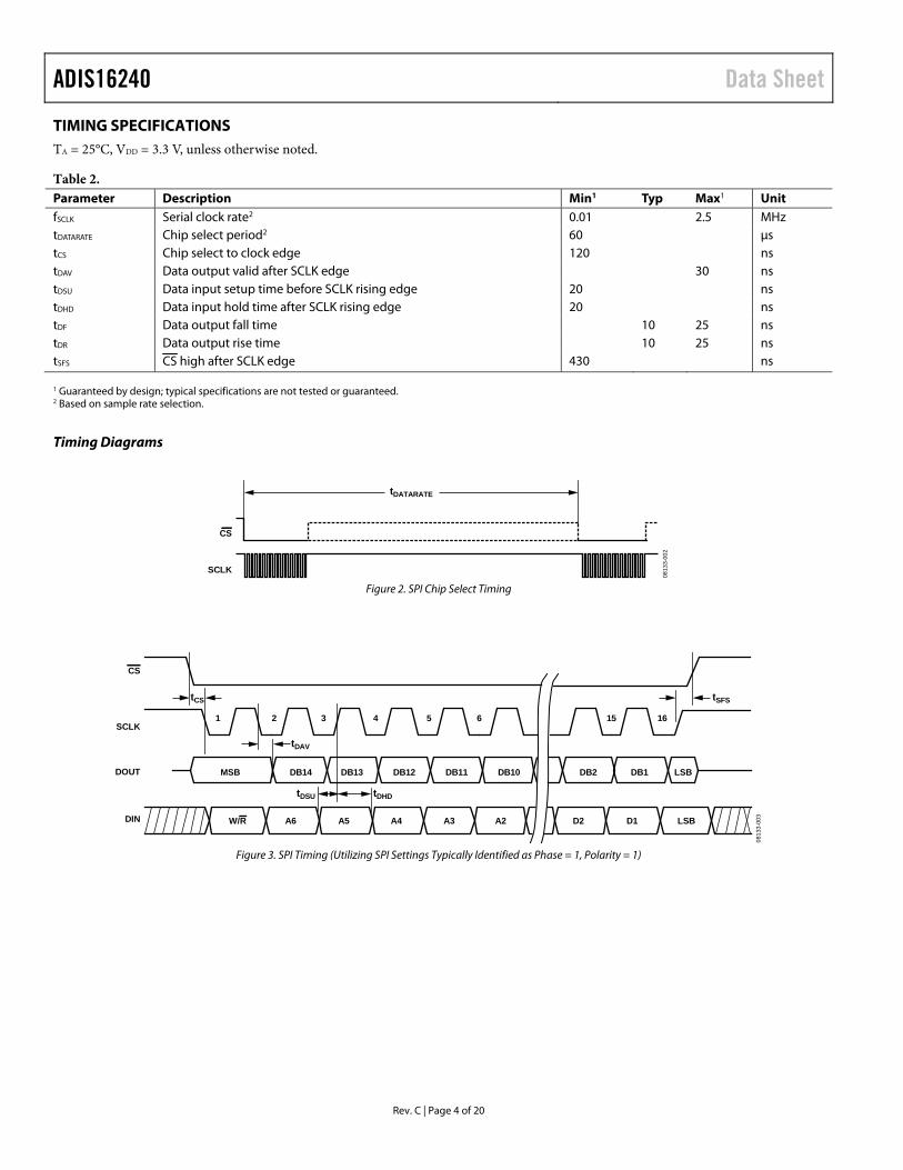
TIMING SPECIFICATIONS TA = 25°C, VDD = 3.3 V, unless otherwise noted.
Table 2. Parameter Description Min1 Typ Max1 Unit fSCLK Serial clock rate2 0.01 2.5 MHz tDATARATE Chip select period2 60 μs tCS Chip select to clock edge 120 ns tDAV Data output valid after SCLK edge 30 ns tDSU Data input setup time before SCLK rising edge 20 ns tDHD Data input hold time after SCLK rising edge 20 ns tDF Data output fall time 10 25 ns tDR Data output rise time 10 25 ns tSFS CS high after SCLK edge 430 ns 1 Guaranteed by design; typical specifications are not tested or guaranteed. 2 Based on sample rate selection.
Timing Diagrams
CS
SCLK
tDATARATE
0813
3-00
2
Figure 2. SPI Chip Select Timing
CS
SCLK
DOUT
DIN
1 2 3 4 5 6 15 16
W/R A5A6 A4 A3 A2 D2
MSB DB14
D1 LSB
DB13 DB12 DB10DB11 DB2 LSBDB1
tCS tSFS
tDAV
tDHDtDSU
0813
3-00
3
Figure 3. SPI Timing (Utilizing SPI Settings Typically Identified as Phase = 1, Polarity = 1)
Data Sheet ADIS16240
Rev. C | Page 5 of 20
ABSOLUTE MAXIMUM RATINGS Table 3. Parameter Rating Acceleration
Any Axis, Unpowered 2000 g Any Axis, Powered 2000 g
VDD to GND −0.3 V to +3.6 V Digital Input Voltage to GND −0.3 V to VDD + 0.3 V Analog Inputs to GND −0.3 V to VDD + 0.3 V Operating Temperature Range −40°C to +85°C Storage Temperature Range −65°C to +150°C
Stresses above those listed under Absolute Maximum Ratings may cause permanent damage to the device. This is a stress rating only; functional operation of the device at these or any other conditions above those indicated in the operational section of this specification is not implied. Exposure to absolute maximum rating conditions for extended periods may affect device reliability.
ESD CAUTION
ADIS16240 Data Sheet
Rev. C | Page 6 of 20
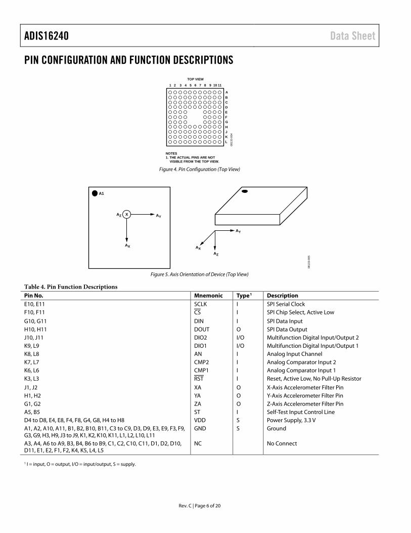
PIN CONFIGURATION AND FUNCTION DESCRIPTIONS
0813
3-00
4
21 4 5 6 9 10 113 7 8
AB
TOP VIEW
NOTES1. THE ACTUAL PINS ARE NOT VISIBLE FROM THE TOP VIEW.
CDEFG
JH
KL
Figure 4. Pin Configuration (Top View)
AZ
A1
AY
AX
AZ
AY
AX
0813
3-00
5
X
Figure 5. Axis Orientation of Device (Top View)
Table 4. Pin Function Descriptions Pin No. Mnemonic Type1 Description E10, E11 SCLK I SPI Serial Clock F10, F11 CS I SPI Chip Select, Active Low
G10, G11 DIN I SPI Data Input H10, H11 DOUT O SPI Data Output J10, J11 DIO2 I/O Multifunction Digital Input/Output 2 K9, L9 DIO1 I/O Multifunction Digital Input/Output 1 K8, L8 AN I Analog Input Channel K7, L7 CMP2 I Analog Comparator Input 2 K6, L6 CMP1 I Analog Comparator Input 1 K3, L3 RST I Reset, Active Low, No Pull-Up Resistor
J1, J2 XA O X-Axis Accelerometer Filter Pin H1, H2 YA O Y-Axis Accelerometer Filter Pin G1, G2 ZA O Z-Axis Accelerometer Filter Pin A5, B5 ST I Self-Test Input Control Line D4 to D8, E4, E8, F4, F8, G4, G8, H4 to H8 VDD S Power Supply, 3.3 V A1, A2, A10, A11, B1, B2, B10, B11, C3 to C9, D3, D9, E3, E9, F3, F9, G3, G9, H3, H9, J3 to J9, K1, K2, K10, K11, L1, L2, L10, L11
GND S Ground
A3, A4, A6 to A9, B3, B4, B6 to B9, C1, C2, C10, C11, D1, D2, D10, D11, E1, E2, F1, F2, K4, K5, L4, L5
NC No Connect
1 I = input, O = output, I/O = input/output, S = supply.
Data Sheet ADIS16240
Rev. C | Page 7 of 20
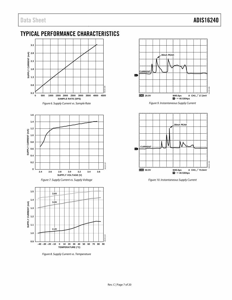
TYPICAL PERFORMANCE CHARACTERISTICS
0.3
0.8
1.3
1.8
2.3
2.8
3.3
0 500 1000 1500 2000 2500 3000 3500 4000 4500
SUPP
LY C
UR
REN
T (m
A)
SAMPLE RATE (SPS)
0813
3-10
6
Figure 6. Supply Current vs. Sample Rate
0.2
0
0.4
0.6
0.8
1.0
1.2
SUPP
LY C
UR
REN
T (m
A)
1.4
1.6
2.4 2.6 2.8 3.0SUPPLY VOLTAGE (V)
3.2 3.4 3.6
0813
3-10
7
Figure 7. Supply Current vs. Supply Voltage
0.9
1.0
1.1
1.2
1.3
1.4
1.5
–40 –30 –20 –10 0 10 20 30 40 50 60 70 80 90
SUPP
LY C
UR
REN
T (m
A)
TEMPERATURE (°C)
3.0V
3.6V
0813
3-11
0
2.4V
Figure 8. Supply Current vs. Temperature
0813
3-10
8
CH1 20.0V M40.0µs A CH1 17.2mV
1
T 40.5304µs
CURRENT
30mA PEAK
Figure 9. Instantaneous Supply Current
0813
3-10
9
CH1 50.0V M40.0µs A CH1 73.0mV
1
T 40.5304µs
CURRENT
30mA PEAK
Figure 10. Instantaneous Supply Current
ADIS16240 Data Sheet
Rev. C | Page 8 of 20
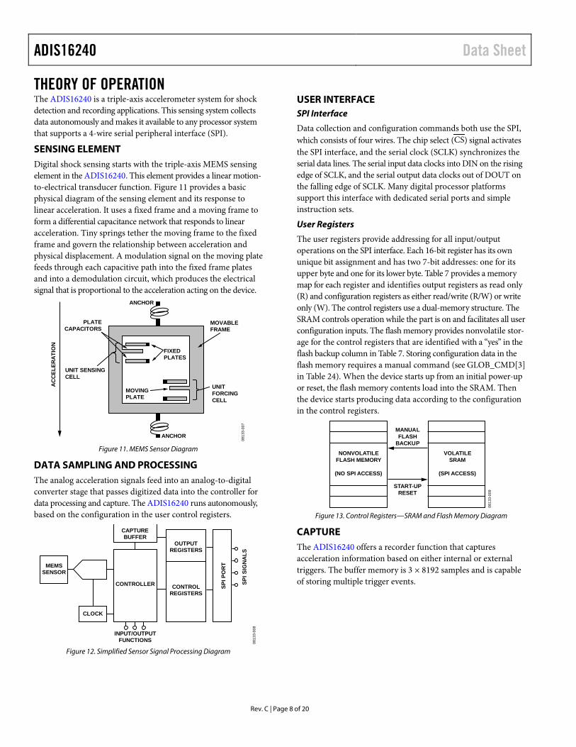
THEORY OF OPERATION The ADIS16240 is a triple-axis accelerometer system for shock detection and recording applications. This sensing system collects data autonomously and makes it available to any processor system that supports a 4-wire serial peripheral interface (SPI).
SENSING ELEMENT Digital shock sensing starts with the triple-axis MEMS sensing element in the ADIS16240. This element provides a linear motion-to-electrical transducer function. Figure 11 provides a basic physical diagram of the sensing element and its response to linear acceleration. It uses a fixed frame and a moving frame to form a differential capacitance network that responds to linear acceleration. Tiny springs tether the moving frame to the fixed frame and govern the relationship between acceleration and physical displacement. A modulation signal on the moving plate feeds through each capacitive path into the fixed frame plates and into a demodulation circuit, which produces the electrical signal that is proportional to the acceleration acting on the device.
MOVABLEFRAME
A
CC
ELER
ATI
ON
UNITFORCINGCELL
UNIT SENSINGCELL
MOVINGPLATE
FIXEDPLATES
PLATECAPACITORS
ANCHOR
ANCHOR
0813
3-00
7
Figure 11. MEMS Sensor Diagram
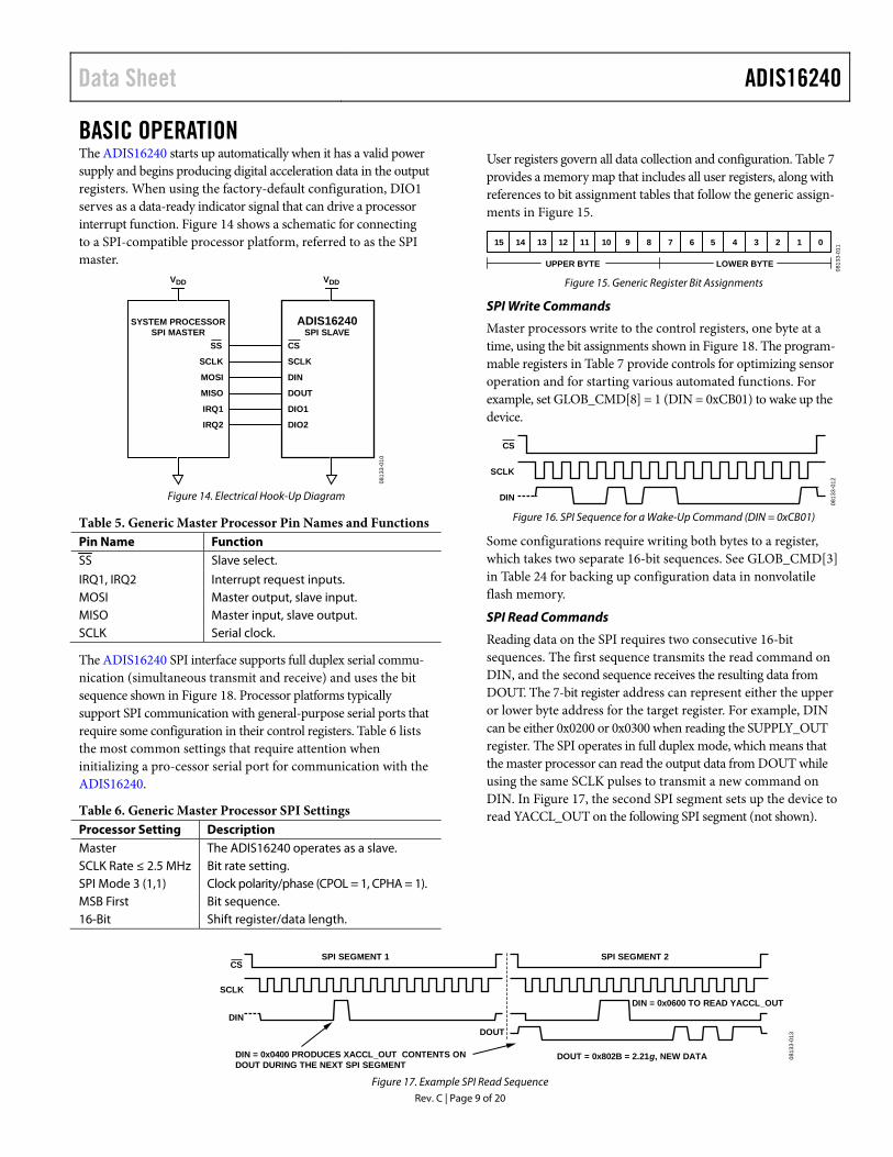
DATA SAMPLING AND PROCESSING The analog acceleration signals feed into an analog-to-digital converter stage that passes digitized data into the controller for data processing and capture. The ADIS16240 runs autonomously, based on the configuration in the user control registers.
MEMSSENSOR
CLOCK
CONTROLLER
INPUT/OUTPUTFUNCTIONS
CAPTUREBUFFER
CONTROLREGISTERS
SPI S
IGN
ALS
SPI P
OR
T
OUTPUTREGISTERS
0813
3-00
8
Figure 12. Simplified Sensor Signal Processing Diagram
USER INTERFACE SPI Interface
Data collection and configuration commands both use the SPI, which consists of four wires. The chip select (CS) signal activates the SPI interface, and the serial clock (SCLK) synchronizes the serial data lines. The serial input data clocks into DIN on the rising edge of SCLK, and the serial output data clocks out of DOUT on the falling edge of SCLK. Many digital processor platforms support this interface with dedicated serial ports and simple instruction sets.
User Registers
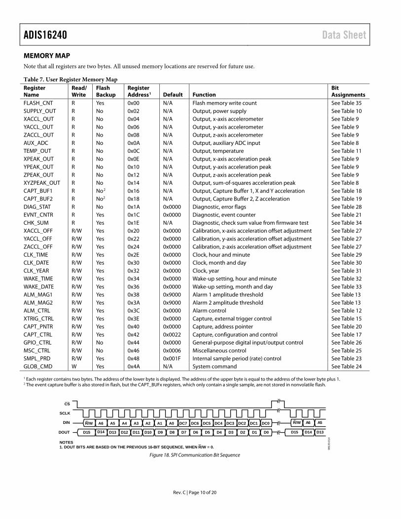
The user registers provide addressing for all input/output operations on the SPI interface. Each 16-bit register has its own unique bit assignment and has two 7-bit addresses: one for its upper byte and one for its lower byte. Table 7 provides a memory map for each register and identifies output registers as read only (R) and configuration registers as either read/write (R/W) or write only (W). The control registers use a dual-memory structure. The SRAM controls operation while the part is on and facilitates all user configuration inputs. The flash memory provides nonvolatile stor-age for the control registers that are identified with a “yes” in the flash backup column in Table 7. Storing configuration data in the flash memory requires a manual command (see GLOB_CMD[3] in Table 24). When the device starts up from an initial power-up or reset, the flash memory contents load into the SRAM. Then the device starts producing data according to the configuration in the control registers.
NONVOLATILEFLASH MEMORY
(NO SPI ACCESS)
MANUALFLASH
BACKUP
START-UPRESET
VOLATILESRAM
(SPI ACCESS)
0813
3-00
9
Figure 13. Control Registers—SRAM and Flash Memory Diagram
CAPTURE The ADIS16240 offers a recorder function that captures acceleration information based on either internal or external triggers. The buffer memory is 3 × 8192 samples and is capable of storing multiple trigger events.
Data Sheet ADIS16240
Rev. C | Page 9 of 20
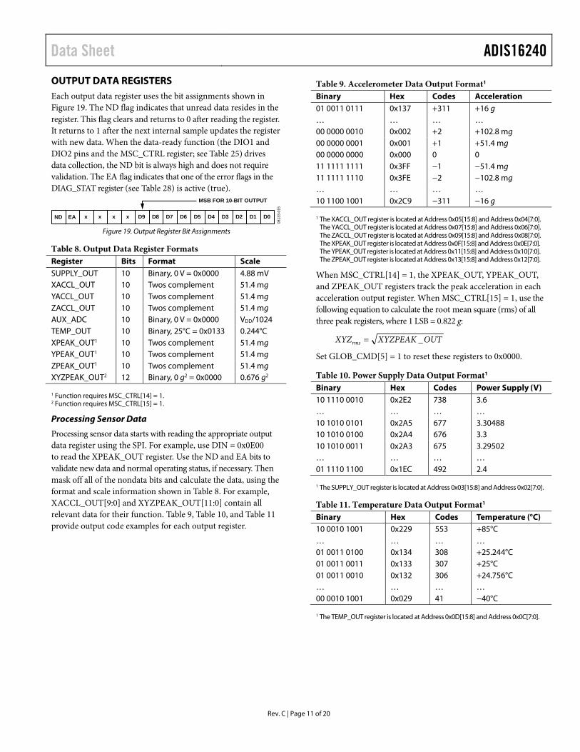
BASIC OPERATION The ADIS16240 starts up automatically when it has a valid power supply and begins producing digital acceleration data in the output registers. When using the factory-default configuration, DIO1 serves as a data-ready indicator signal that can drive a processor interrupt function. Figure 14 shows a schematic for connecting to a SPI-compatible processor platform, referred to as the SPI master.
CS
ADIS16240SPI SLAVE
SCLK
DIN
DOUT
DIO1
DIO2
SS
VDD VDD
SYSTEM PROCESSORSPI MASTER
SCLK
MOSI
MISO
IRQ1
IRQ2
0813
3-01
0
Figure 14. Electrical Hook-Up Diagram
Table 5. Generic Master Processor Pin Names and Functions Pin Name Function SS Slave select.
IRQ1, IRQ2 Interrupt request inputs. MOSI Master output, slave input. MISO Master input, slave output. SCLK Serial clock.
The ADIS16240 SPI interface supports full duplex serial commu-nication (simultaneous transmit and receive) and uses the bit sequence shown in Figure 18. Processor platforms typically support SPI communication with general-purpose serial ports that require some configuration in their control registers. Table 6 lists the most common settings that require attention when initializing a pro-cessor serial port for communication with the ADIS16240.
Table 6. Generic Master Processor SPI Settings Processor Setting Description Master The ADIS16240 operates as a slave. SCLK Rate ≤ 2.5 MHz Bit rate setting. SPI Mode 3 (1,1) Clock polarity/phase (CPOL = 1, CPHA = 1). MSB First Bit sequence. 16-Bit Shift register/data length.
User registers govern all data collection and configuration. Table 7 provides a memory map that includes all user registers, along with references to bit assignment tables that follow the generic assign-ments in Figure 15.
UPPER BYTE
15 14 13 12 11 10 9 8 7 6 5 4 3 2 1 0
LOWER BYTE
0813
3-01
1
Figure 15. Generic Register Bit Assignments
SPI Write Commands
Master processors write to the control registers, one byte at a time, using the bit assignments shown in Figure 18. The program-mable registers in Table 7 provide controls for optimizing sensor operation and for starting various automated functions. For example, set GLOB_CMD[8] = 1 (DIN = 0xCB01) to wake up the device.
CS
DIN
SCLK
0813
3-01
2
Figure 16. SPI Sequence for a Wake-Up Command (DIN = 0xCB01)
Some configurations require writing both bytes to a register, which takes two separate 16-bit sequences. See GLOB_CMD[3] in Table 24 for backing up configuration data in nonvolatile flash memory.
SPI Read Commands
Reading data on the SPI requires two consecutive 16-bit sequences. The first sequence transmits the read command on DIN, and the second sequence receives the resulting data from DOUT. The 7-bit register address can represent either the upper or lower byte address for the target register. For example, DIN can be either 0x0200 or 0x0300 when reading the SUPPLY_OUT register. The SPI operates in full duplex mode, which means that the master processor can read the output data from DOUT while using the same SCLK pulses to transmit a new command on DIN. In Figure 17, the second SPI segment sets up the device to read YACCL_OUT on the following SPI segment (not shown).
CS
DIN
SCLK
DIN = 0x0400 PRODUCES XACCL_OUT CONTENTS ONDOUT DURING THE NEXT SPI SEGMENT
DOUT
SPI SEGMENT 1 SPI SEGMENT 2
DOUT = 0x802B = 2.21g, NEW DATA
DIN = 0x0600 TO READ YACCL_OUT
0813
3-01
3
Figure 17. Example SPI Read Sequence
ADIS16240 Data Sheet
Rev. C | Page 10 of 20
MEMORY MAP Note that all registers are two bytes. All unused memory locations are reserved for future use.
Table 7. User Register Memory Map Register Name
Read/ Write
Flash Backup
Register Address1 Default Function
Bit Assignments
FLASH_CNT R Yes 0x00 N/A Flash memory write count See Table 35 SUPPLY_OUT R No 0x02 N/A Output, power supply See Table 10 XACCL_OUT R No 0x04 N/A Output, x-axis accelerometer See Table 9 YACCL_OUT R No 0x06 N/A Output, y-axis accelerometer See Table 9 ZACCL_OUT R No 0x08 N/A Output, z-axis accelerometer See Table 9 AUX_ADC R No 0x0A N/A Output, auxiliary ADC input See Table 8 TEMP_OUT R No 0x0C N/A Output, temperature See Table 11 XPEAK_OUT R No 0x0E N/A Output, x-axis acceleration peak See Table 9 YPEAK_OUT R No 0x10 N/A Output, y-axis acceleration peak See Table 9 ZPEAK_OUT R No 0x12 N/A Output, z-axis acceleration peak See Table 9 XYZPEAK_OUT R No 0x14 N/A Output, sum-of-squares acceleration peak See Table 8 CAPT_BUF1 R No2 0x16 N/A Output, Capture Buffer 1, X and Y acceleration See Table 18 CAPT_BUF2 R No2 0x18 N/A Output, Capture Buffer 2, Z acceleration See Table 19 DIAG_STAT R No 0x1A 0x0000 Diagnostic, error flags See Table 28 EVNT_CNTR R Yes 0x1C 0x0000 Diagnostic, event counter See Table 21 CHK_SUM R Yes 0x1E N/A Diagnostic, check sum value from firmware test See Table 34 XACCL_OFF R/W Yes 0x20 0x0000 Calibration, x-axis acceleration offset adjustment See Table 27 YACCL_OFF R/W Yes 0x22 0x0000 Calibration, y-axis acceleration offset adjustment See Table 27 ZACCL_OFF R/W Yes 0x24 0x0000 Calibration, z-axis acceleration offset adjustment See Table 27 CLK_TIME R/W Yes 0x2E 0x0000 Clock, hour and minute See Table 29 CLK_DATE R/W Yes 0x30 0x0000 Clock, month and day See Table 30 CLK_YEAR R/W Yes 0x32 0x0000 Clock, year See Table 31 WAKE_TIME R/W Yes 0x34 0x0000 Wake-up setting, hour and minute See Table 32 WAKE_DATE R/W Yes 0x36 0x0000 Wake-up setting, month and day See Table 33 ALM_MAG1 R/W Yes 0x38 0x9000 Alarm 1 amplitude threshold See Table 13 ALM_MAG2 R/W Yes 0x3A 0x9000 Alarm 2 amplitude threshold See Table 13 ALM_CTRL R/W Yes 0x3C 0x0000 Alarm control See Table 12 XTRIG_CTRL R/W Yes 0x3E 0x0000 Capture, external trigger control See Table 15 CAPT_PNTR R/W Yes 0x40 0x0000 Capture, address pointer See Table 20 CAPT_CTRL R/W Yes 0x42 0x0022 Capture, configuration and control See Table 17 GPIO_CTRL R/W No 0x44 0x0000 General-purpose digital input/output control See Table 26 MSC_CTRL R/W No 0x46 0x0006 Miscellaneous control See Table 25 SMPL_PRD R/W Yes 0x48 0x001F Internal sample period (rate) control See Table 23 GLOB_CMD W Yes 0x4A N/A System command See Table 24 1 Each register contains two bytes. The address of the lower byte is displayed. The address of the upper byte is equal to the address of the lower byte plus 1. 2 The event capture buffer is also stored in flash, but the CAPT_BUFx registers, which only contain a single sample, are not stored in nonvolatile flash.
R/W R/WA6 A5 A4 A3 A2 A1 A0 DC7 DC6 DC5 DC4 DC3 DC2 DC1 DC0
D0D1D2D3D4D5D6D7D8D9D10D11D12D13D14D15
NOTES1. DOUT BITS ARE BASED ON THE PREVIOUS 16-BIT SEQUENCE, WHEN R/W = 0.
CS
SCLK
DIN
DOUT
A6 A5
D13D14D15
0813
3-01
4
Figure 18. SPI Communication Bit Sequence
Data Sheet ADIS16240
Rev. C | Page 11 of 20
OUTPUT DATA REGISTERS Each output data register uses the bit assignments shown in Figure 19. The ND flag indicates that unread data resides in the register. This flag clears and returns to 0 after reading the register. It returns to 1 after the next internal sample updates the register with new data. When the data-ready function (the DIO1 and DIO2 pins and the MSC_CTRL register; see Table 25) drives data collection, the ND bit is always high and does not require validation. The EA flag indicates that one of the error flags in the DIAG_STAT register (see Table 28) is active (true).
MSB FOR 10-BIT OUTPUT
ND EA x x x x D9 D8 D7 D6 D5 D4 D3 D2 D1 D0
0813
3-01
5
Figure 19. Output Register Bit Assignments
Table 8. Output Data Register Formats Register Bits Format Scale SUPPLY_OUT 10 Binary, 0 V = 0x0000 4.88 mV XACCL_OUT 10 Twos complement 51.4 mg YACCL_OUT 10 Twos complement 51.4 mg ZACCL_OUT 10 Twos complement 51.4 mg AUX_ADC 10 Binary, 0 V = 0x0000 VDD/1024 TEMP_OUT 10 Binary, 25°C = 0x0133 0.244°C XPEAK_OUT1 10 Twos complement 51.4 mg YPEAK_OUT1 10 Twos complement 51.4 mg ZPEAK_OUT1 10 Twos complement 51.4 mg XYZPEAK_OUT2 12 Binary, 0 g2 = 0x0000 0.676 g2
1 Function requires MSC_CTRL[14] = 1. 2 Function requires MSC_CTRL[15] = 1.
Processing Sensor Data
Processing sensor data starts with reading the appropriate output data register using the SPI. For example, use DIN = 0x0E00 to read the XPEAK_OUT register. Use the ND and EA bits to validate new data and normal operating status, if necessary. Then mask off all of the nondata bits and calculate the data, using the format and scale information shown in Table 8. For example, XACCL_OUT[9:0] and XYZPEAK_OUT[11:0] contain all relevant data for their function. Table 9, Table 10, and Table 11 provide output code examples for each output register.
Table 9. Accelerometer Data Output Format1 Binary Hex Codes Acceleration 01 0011 0111 0x137 +311 +16 g … … … … 00 0000 0010 0x002 +2 +102.8 mg 00 0000 0001 0x001 +1 +51.4 mg 00 0000 0000 0x000 0 0 11 1111 1111 0x3FF −1 −51.4 mg 11 1111 1110 0x3FE −2 −102.8 mg … … … … 10 1100 1001 0x2C9 −311 −16 g 1 The XACCL_OUT register is located at Address 0x05[15:8] and Address 0x04[7:0].
The YACCL_OUT register is located at Address 0x07[15:8] and Address 0x06[7:0]. The ZACCL_OUT register is located at Address 0x09[15:8] and Address 0x08[7:0]. The XPEAK_OUT register is located at Address 0x0F[15:8] and Address 0x0E[7:0]. The YPEAK_OUT register is located at Address 0x11[15:8] and Address 0x10[7:0]. The ZPEAK_OUT register is located at Address 0x13[15:8] and Address 0x12[7:0].
When MSC_CTRL[14] = 1, the XPEAK_OUT, YPEAK_OUT, and ZPEAK_OUT registers track the peak acceleration in each acceleration output register. When MSC_CTRL[15] = 1, use the following equation to calculate the root mean square (rms) of all three peak registers, where 1 LSB = 0.822 g:
OUTXYZPEAKXYZrms _=
Set GLOB_CMD[5] = 1 to reset these registers to 0x0000.
Table 10. Power Supply Data Output Format1 Binary Hex Codes Power Supply (V) 10 1110 0010 0x2E2 738 3.6 … … … … 10 1010 0101 0x2A5 677 3.30488 10 1010 0100 0x2A4 676 3.3 10 1010 0011 0x2A3 675 3.29502 … … … … 01 1110 1100 0x1EC 492 2.4 1 The SUPPLY_OUT register is located at Address 0x03[15:8] and Address 0x02[7:0].
Table 11. Temperature Data Output Format1 Binary Hex Codes Temperature (°C) 10 0010 1001 0x229 553 +85°C … … … … 01 0011 0100 0x134 308 +25.244°C 01 0011 0011 0x133 307 +25°C 01 0011 0010 0x132 306 +24.756°C … … … … 00 0010 1001 0x029 41 −40°C 1 The TEMP_OUT register is located at Address 0x0D[15:8] and Address 0x0C[7:0].
ADIS16240 Data Sheet
Rev. C | Page 12 of 20
EVENT RECORDER The ADIS16240 provides a 3 × 8192 (8-bit) buffer memory for capturing and storing (in flash) transient acceleration data on all three axes (x, y, and z). There are a number of user controls for tailoring the event recorder for optimal system-level operation. Alarm 1 and Alarm 2 provide internal and external trigger options for starting a data capture sequence.
Internal Trigger Setup
Select the trigger data source for Alarm 1 and Alarm 2 using ALM_CTRL[15:8] (see Table 12). The ALM_MAG1 and ALM_ MAG2 registers contain threshold magnitude and direction settings for Alarm 1 and Alarm 2, respectively. The format for the data bits in these registers matches the trigger data source, which is set using ALM_CTRL[15:8]. For example, if ALM_ CTRL[15:12] equals 0010, then the format matches that of XACCL_OUT: 10-bit, twos complement, with 1 LSB = 51.4 mg of acceleration.
Table 12. ALM_CTRL Register Bit Descriptions1
Bit Description (Default = 0x0000) [15:12] Alarm 2 source selection 0000 = disabled 0001 = power supply voltage (SUPPLY_OUT) 0010 = x acceleration (XACCL_OUT) 0011 = y acceleration (YACCL_OUT) 0100 = z acceleration (ZACCL_OUT) 0101 = auxiliary ADC voltage (AUX_ADC) 0110 = temperature (TEMP_OUT) 0111 = XYZ peak acceleration (XYZPEAK_OUT) 1000 = external trigger [11:8] Alarm 1 source selection (same as Alarm 2) [7:6] Unused 5 Alarm 2 capture trigger: 1 = enabled, 0 = disabled 4 Alarm 1 capture trigger: 1 = enabled, 0 = disabled 3 Unused 2 Alarm indicator enable: 1 = enabled, 0 = disabled 1 Alarm indicator polarity: 1 = positive, 0 = negative 0 Alarm indicator pin: 1 = DIO2, 0 = DIO1 1 The ALM_CTRL register is located at Address 0x3D[15:8] and Address 0x3C[7:0].
Table 13. ALM_MAG1, ALM_MAG2 Register Bit Descriptions1 Bit Description (Default = 0x9000) 15 Threshold direction
1 = active for output greater than alarm magnitude 0 = inactive for output less than alarm magnitude
14 Unused [13:0] Trigger threshold; bit format matches that of the register
selected by ALM_CTRL[15:8] but is unsigned. 1 The ALM_MAG1 register is located at Address 0x39[15:8] and Address 0x38[7:0].
The ALM_MAG2 register is located at Address 0x3B[15:8] and Address 0x3A[7:0].
Table 14. Internal Trigger Setup Example DIN Description 0xBD44 Set Alarm 1 and Alarm 2 to ZACCL_OUT 0xB980, 0xB832
Set Alarm 1 to trigger on a measured acceleration that has a magnitude of >2.57 g
0xBB00, 0xBA0A
Set Alarm 2 to trigger on a measured acceleration that has a magnitude of <0.5 g
0xBC37 Activate Alarm 1 and Alarm 2 to trigger capture events, and configure DIO2 as a positive alarm indicator output.
External Trigger Setup
ALM_CTRL[15:8] and XTRIG_CTRL (see Table 15) provide all of the settings needed to govern the use of the comparator pins (CMP1, CMP2) as external trigger inputs.
Table 15. XTRIG_CTRL Register Bit Descriptions1 Bit Description (Default = 0x0000) [15:8] Unused 7 External Trigger 1 direction: 0 = <, 1 = > 6 External Trigger 2 direction: 0 = <, 1 = > 5 External Trigger 1 enable: 1 = enabled, 0 = disabled 4 External Trigger 2 enable: 1 = enabled, 0 = disabled [3:0] External trigger-level setting (TL), binary format Note that trigger threshold = TL × supply/24 1 The XTRIG_CTRL register is located at Address 0x3F[15:8] and Address 0x3E[7:0].
Table 16. External Trigger Setup Example DIN Description 0xBD80 Set Alarm 2 to an external trigger (ALM_CTRL) 0xBE1C Activate and set CMP2 to trigger on signals that are
greater than one-half of the supply voltage (XTRIG_CTRL) 0xBC20 Activate Alarm 2 to trigger data capture (ALM_CTRL)
If the device is in standby mode, an external trigger on CMD1 or CMD2 awakens the device and initiates an event capture. The first sample is taken 0.2 ms + sample period (SMPL_PRD[7:0]) after the trigger edge.
Buffer Memory Configuration
CAPT_CTRL (see Table 17) manages the buffer memory for the event recorder using two programmable controls: event length and pretrigger length.
Table 17. CAPT_CTRL Register Bit Descriptions1 Bit Description (Default = 0x0022) [15:8] Unused [7:4] Pretrigger length control factor (P), binary format 3 Unused [2:0] Event length control factor (T), binary format 1 The CAPT_CTRL register is located at Address 0x43[15:8] and Address 0x42[7:0].
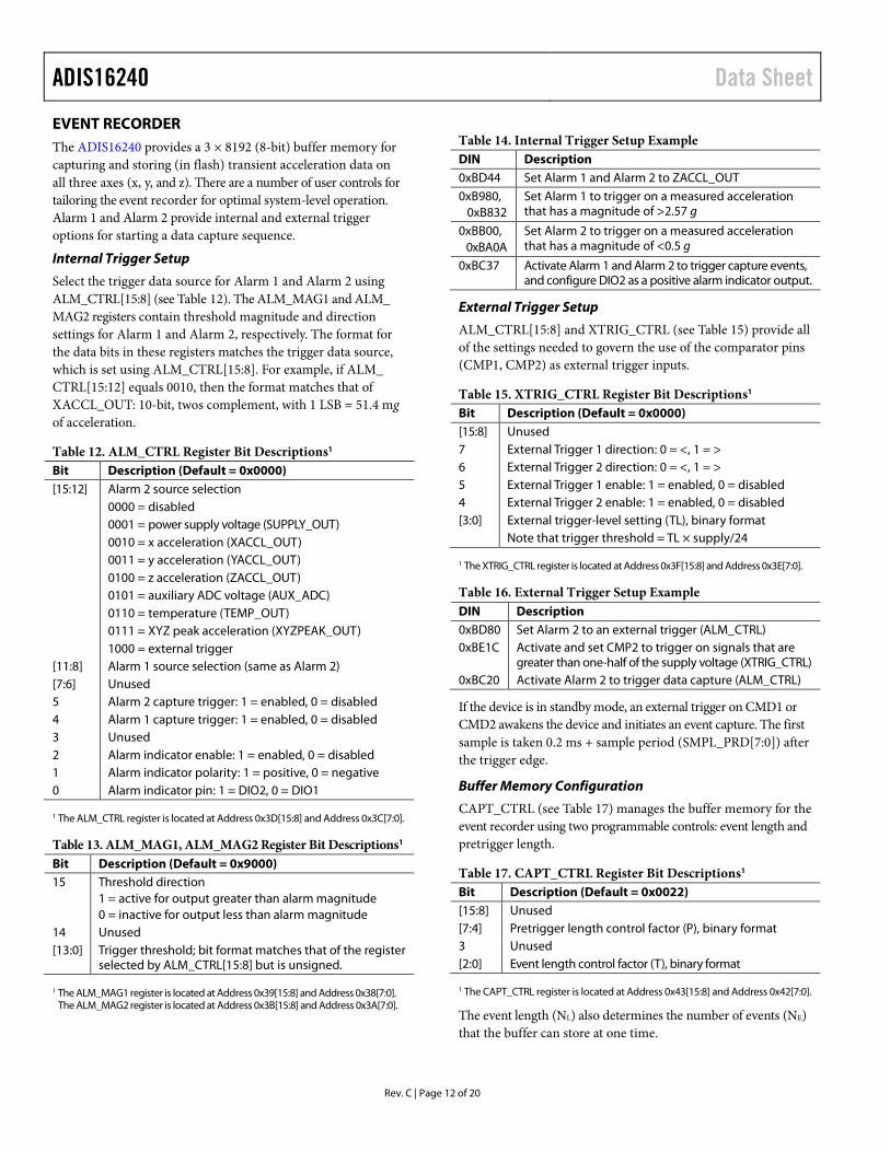
The event length (NL) also determines the number of events (NE) that the buffer can store at one time.
Data Sheet ADIS16240
Rev. C | Page 13 of 20
8192SAMPLES
EVENT 1
EVENT NE
NL
NL =2T
1024
NE = 8 × 2T
EVENT 2
0813
3-01
6
Figure 20. Event Storage in Buffer Memory
For example, if CAPT_CTRL[2:0] = 100, then T = 4, which organizes the buffer memory into 128 events of 64 samples each.
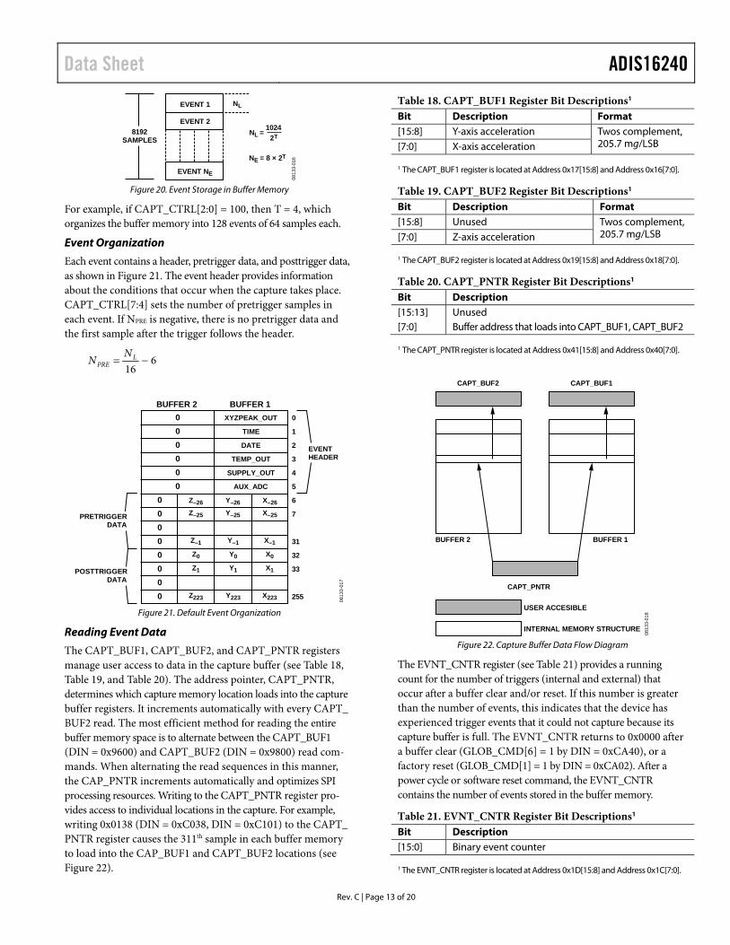
Event Organization
Each event contains a header, pretrigger data, and posttrigger data, as shown in Figure 21. The event header provides information about the conditions that occur when the capture takes place. CAPT_CTRL[7:4] sets the number of pretrigger samples in each event. If NPRE is negative, there is no pretrigger data and the first sample after the trigger follows the header.
616
LPRE
NN
XYZPEAK_OUT
TIME
DATE
TEMP_OUT
SUPPLY_OUT
AUX_ADC
000000
Z–26
Z–25
Z–1
Z0
Z1
Y–1
Y0
Y1
X–1
X0
X1
Z223 Y223 X223
Y–26
Y–25
X–26
X–25
00
000
0
0
0255
0
1
2
3
4
5
6
7
31
32
33POSTTRIGGERDATA
PRETRIGGERDATA
EVENTHEADER
BUFFER 2 BUFFER 1
0813
3-01
7
Figure 21. Default Event Organization
Reading Event Data
The CAPT_BUF1, CAPT_BUF2, and CAPT_PNTR registers manage user access to data in the capture buffer (see Table 18, Table 19, and Table 20). The address pointer, CAPT_PNTR, determines which capture memory location loads into the capture buffer registers. It increments automatically with every CAPT_ BUF2 read. The most efficient method for reading the entire buffer memory space is to alternate between the CAPT_BUF1 (DIN = 0x9600) and CAPT_BUF2 (DIN = 0x9800) read com-mands. When alternating the read sequences in this manner, the CAP_PNTR increments automatically and optimizes SPI processing resources. Writing to the CAPT_PNTR register pro-vides access to individual locations in the capture. For example, writing 0x0138 (DIN = 0xC038, DIN = 0xC101) to the CAPT_ PNTR register causes the 311th sample in each buffer memory to load into the CAP_BUF1 and CAPT_BUF2 locations (see Figure 22).
Table 18. CAPT_BUF1 Register Bit Descriptions1
Bit Description Format [15:8] Y-axis acceleration Twos complement,
205.7 mg/LSB [7:0] X-axis acceleration 1 The CAPT_BUF1 register is located at Address 0x17[15:8] and Address 0x16[7:0].
Table 19. CAPT_BUF2 Register Bit Descriptions1 Bit Description Format [15:8] Unused Twos complement,
205.7 mg/LSB [7:0] Z-axis acceleration 1 The CAPT_BUF2 register is located at Address 0x19[15:8] and Address 0x18[7:0].
Table 20. CAPT_PNTR Register Bit Descriptions1 Bit Description [15:13] Unused [7:0] Buffer address that loads into CAPT_BUF1, CAPT_BUF2 1 The CAPT_PNTR register is located at Address 0x41[15:8] and Address 0x40[7:0].
CAPT_PNTR
CAPT_BUF2
USER ACCESIBLE
INTERNAL MEMORY STRUCTURE
CAPT_BUF1
BUFFER 2 BUFFER 1
0813
3-01
8
Figure 22. Capture Buffer Data Flow Diagram
The EVNT_CNTR register (see Table 21) provides a running count for the number of triggers (internal and external) that occur after a buffer clear and/or reset. If this number is greater than the number of events, this indicates that the device has experienced trigger events that it could not capture because its capture buffer is full. The EVNT_CNTR returns to 0x0000 after a buffer clear (GLOB_CMD[6] = 1 by DIN = 0xCA40), or a factory reset (GLOB_CMD[1] = 1 by DIN = 0xCA02). After a power cycle or software reset command, the EVNT_CNTR contains the number of events stored in the buffer memory.
Table 21. EVNT_CNTR Register Bit Descriptions1 Bit Description [15:0] Binary event counter 1 The EVNT_CNTR register is located at Address 0x1D[15:8] and Address 0x1C[7:0].
ADIS16240 Data Sheet
Rev. C | Page 14 of 20
Transient Behavior During Capture
During capture events, the device consumes an increased amount of current for a short period. Following a capture event, sampling suspends and the SPI commands are ignored by the sensor for the pause times that are listed in Table 22.
Table 22. Postcapture Operation Pause Times Event Length (Samples) Pause Time (ms) <64 2 128 4 256 8 512 16 1024 33
OPERATIONAL CONTROL Internal Sample Rate
The SMPL_PRD register (see Table 23) provides a user control for sample rate adjustment, using the following equation:
fS = )1(
32768+SRN
For example, set SMPL_PRD[7:0] = 0x07 (DIN = 0xC807) to configure the ADIS16240 to operate at its maximum sample rate of 4096 SPS. Note that the sample rate affects power dis-sipation and peak resolution during event capture.
Table 23. SMPL_PRD Register Bit Descriptions1 Bit Description (Default = 0x001F) [15:0] Sample rate scale factor, binary format (NSR) 1 The SMPL_PRD register is located at Address 0x49[15:8] and Address 0x48[7:0].
Global Commands
For convenience, the GLOB_CMD register (see Table 24) provides an array of single-write commands. Setting the assigned bit to 1 activates each function, right after the 16th SCLK in the SPI com-munication sequence. When the function completes, the bit restores itself to 0. All commands in the GLOB_CMD register require the power supply to be within normal limits for the execution times listed in Table 24. The execution times reflect the factory default configuration, where applicable, and describe the time required to return to normal operation. For example, set GLOB_CMD[2] = 1 (DIN = 0xCA04) to place the part in standby mode. Set GLOB_CMD[8] = 1 (DIN = 0xCB01) to wake up the device and return to normal operation.
Input/Output Lines
The ADIS16240 provides two general-purpose digital input/ output lines that offer several functions. When using the factory-default configuration, MSC_CTRL[2:0] establishes DIO1 as a positive data-ready output. Change MSC_CTRL[2:0] to 100 (DIN = 0xC604) to make DIO1 a negative data-ready output signal. ALM_CTRL[2:0] offers a control for setting one of the digital signals as an alarm indicator. For example, set ALM_ CTRL[2:0] = 110 (DIN = 0xBC06) to set DIO1 as a positive alarm indicator output signal. When configured as general-
purpose lines, the GPIO_CTRL register configures DIO1 and DIO2. For example, set GPIO_CTRL = 0x0103 (DIN = 0xC403, then 0xC501) to set DIO1 and DIO2 as outputs, with DIO1 in a 1 state and DIO2 in a 0 state. In the event of competing assign-ments, the order of precedence is MSC_CTRL, ALM_CTRL, and GPIO_CTRL.
Table 24. GLOB_CMD Register Bit Descriptions1 Bit Description Execution Time2 [15:9] Unused N/A 8 Wake up from standby mode 0.2 ms 7 Software reset 32 ms 6 Clear capture buffer flash memory 350 ms 5 Clear peak registers N/A 4 Clear DIAG_STAT register N/A 3 Save configuration to flash 24 ms 2 Start standby mode for low power N/A 1 Restore factory-default settings 350 ms 0 Auto-null N/A 1 The GLOB_CMD register is located at Address 0x4B[15:8] and Address 0x4A[7:0]. 2 SPI processing and data sampling suspend for the indicated times.
Table 25. MSC_CTRL Register Bit Descriptions1 Bit Description (Default = 0x0006) 15 Enables sum-of-squares output (XYZPEAK_OUT) 14 Enables peak tracking output (XPEAK_OUT,
YPEAK_OUT, and ZPEAK_OUT) [13:10] Unused 9 No self-test on startup when set to 1 8 Self-test enable: 1 = apply electrostatic force, 0 = disabled [7:3] Unused 2 Data-ready enable: 1 = enabled, 0 = disabled 1 Data-ready polarity: 1 = active high, 0 = active low 0 Data-ready line selection: 1 = DIO2, 0 = DIO1 1 The MSC_CTRL register is located at Address 0x47[15:8] and Address 0x46[7:0].
Table 26. GPIO_CTRL Register Bit Descriptions1 Bit Description (Default = 0x0000) [15:10] Unused 9 General-Purpose I/O Line 2 data level 8 General-Purpose I/O Line 1 data level [7:2] Unused 1 General-Purpose I/O Line 2, data direction control:
1 = output, 0 = input 0 General-Purpose I/O Line 1, data direction control:
1 = output, 0 = input 1 The GPIO_CTRL register is located at Address 0x45[15:8] and Address 0x44[7:0].
Offset Adjustment
The XACCL_OUT, YACCL_OFF, and ZACCL_OFF registers add to the sensor outputs and provide a convenient offset adjust-ment function for each accelerometer output. For example, writing 0x0A to YACCL_OUT[7:0] (DIN = 0xA20A) results in a 514 mg offset adjustment for the YACCL_OUT output data.
Data Sheet ADIS16240
Rev. C | Page 15 of 20
Table 27. XACCL_OFF, YACCL_OFF, ZACCL_OFF1 Bit Description (Default = 0x0000) [15:10] Unused [9:0] Offset, twos complement, 51.4 mg/LSB 1 The XACCL_OFF register is located at Address 0x21[15:8] and Address 0x20[7:0].
The YACCL_OFF register is located at Address 0x23[15:8] and Address 0x22[7:0]. The ZACCL_OFF register is located at Address 0x25[15:8] and Address 0x24[7:0].
Diagnostics
For all of the error flags in the DIAG_STAT register (see Table 28), a 1 identifies an error condition, and a 0 signals normal operation. All of the flags return to 0 after reading DIAG_STAT. If the power supply is still out of range during the next sample cycle, DIAG_ STAT[0] and DIAG_STAT[1] return to 1. DIAG_STAT[9:8] pro-vide flags to check for the alarms with respect to the conditions in the ALM_CTRL and ALM_MAGx registers. DIAG_STAT[6] contains the internal memory checksum result. If the sum of the firmware program memory does not does not match the expected value, this flag reports a 1. The SPI communication flag (DIAG_ STAT[3]) changes to 1 when the number of SCLK pulses during a SPI transfer is not a multiple of 16 when CS goes high.
Table 28. DIAG_STAT Register Bit Descriptions1 Bit Description (Default = 0x0000) [15:10] Unused 9 Alarm 2 status: 1 = alarm active, 0 = alarm inactive 8 Alarm 1 status: 1 = alarm active, 0 = alarm inactive 7 Capture buffer full: 1 = capture buffer is full 6 Flash test, checksum flag: 1 = mismatch, 0 = match 5 Power-on, self-test flag: 1 = failure, 0 = pass 4 Power-on self-test: 1 = in-progress, 0 = complete 3 SPI communications failure: 1 = error, 0 = normal 2 Flash update failure: 1 = failure, 0 = pass 1 Power supply above 3.625 V: 1 = above, 0 = below 0 Power supply below 2.225 V: 1 = below, 0 = above 1 The DIAG_STAT register is located at Address 0x1B[15:8] and Address 0x1A[7:0].
Clock
The CLK_TIME, CLK_DATE, and CLK_YEAR registers provide an internal clock that enables a time entry into the event header and for user access. If CLK_TIME = 0x2231, the time is 22:31, or 10:31 p.m. The CLK_DATE and CLK_YEAR registers follow a similar binary-coded, decimal format.
Table 29. CLK_TIME Register Bit Descriptions1 Bit Description [15:14] Unused [13:12] Hours, 10s digit [11:8] Hours, 1s digit 7 Unused [6:4] Minutes, 10s digit [3:0] Minutes, 1s digit 1 The CLK_TIME register is located at Address 0x2F[15:8] and Address 0x2E[7:0].
Table 30. CLK_DATE Register Bit Descriptions1 Bit Description (Default = 0x0000) [15:13] Unused 12 Month, 10s digit [11:8] Month, 1s digit [7:6] Unused [5:4] Day, 10s digit [3:0] Day, 1s digit 1 The CLK_DATE register is located at Address 0x31[15:8] and Address 0x30[7:0].
Table 31. CLK_YEAR Register Bit Descriptions1 Bit Description (Default = 0x0000) [15:8] Unused [7:4] Year, 10s digit [3:0] Year, 1s digit 1 The CLK_YEAR register is located at Address 0x33[15:8] and Address 0x32[7:0].
The WAKE_TIME and WAKE_DATE registers enable users to program a specific time for the ADIS16240 to exit standby mode. Enable this function by writing the wake-up time and date to these registers.
Table 32. WAKE_TIME Register Bit Descriptions1 Bit Description (Default = 0x0000) 15 Wake time enable (1 = enabled, 0 = disabled) 14 Unused [13:12] Hours, 10s digit [11:8] Hours, 1s digit 7 Unused [6:4] Minutes, 10s digit [3:0] Minutes, 1s digit 1 The WAKE_TIME register is located at Address 0x35[15:8] and Address 0x34[7:0].
Table 33. WAKE_DATE Register Bit Descriptions1 Bit Description (Default = 0x0000) [15:14] Unused [13:12] Month, 10s digit [11:8] Month, 1s digit [7:6] Unused [5:4] Day, 10s digit [3:0] Day, 1s digit 1 The WAKE_DATE register is located at Address 0x37[15:8] and Address 0x36[7:0].
Checksum
Table 34. CHK_SUM Register Bit Descriptions1 Bit Description [15:0] Sum of memory locations used to verify code integrity 1 The CHK_SUM register is located at Address 0x1F[15:8] and Address 0x1E[7:0].
ADIS16240 Data Sheet
Rev. C | Page 16 of 20
Flash Memory Endurance Management
The FLASH_CNT register (see Table 35) tracks the number of flash memory write cycles, to help manage the flash endurance of the ADIS16240 (see Table 1). This register contains a binary counter that increments after every flash memory write cycle, with one exception: event storage. Each event capture will automatically update in its particular flash memory location, but only the first event capture will trigger a complete flash update (all user control registers) and result in the FLASH_CNT incrementing the counter. In addition to the first event capture/storage, activating the auto-null (GLOB_CMD[0]),
factory reset (GLOB_CMD[1]), and manual flash update GLOB_CMD[3] will also result in a manual flash write cycle that causes FLASH_CNT to increment.
Table 35. FLASH_CNT Register Bit Descriptions1 Bit Description [15:0] Binary code, increments with every flash memory write
cycle. 1 The FLASH_CNT register is located at Address 0x01[15:8] and Address
0x00[7:0].
Data Sheet ADIS16240
Rev. C | Page 17 of 20
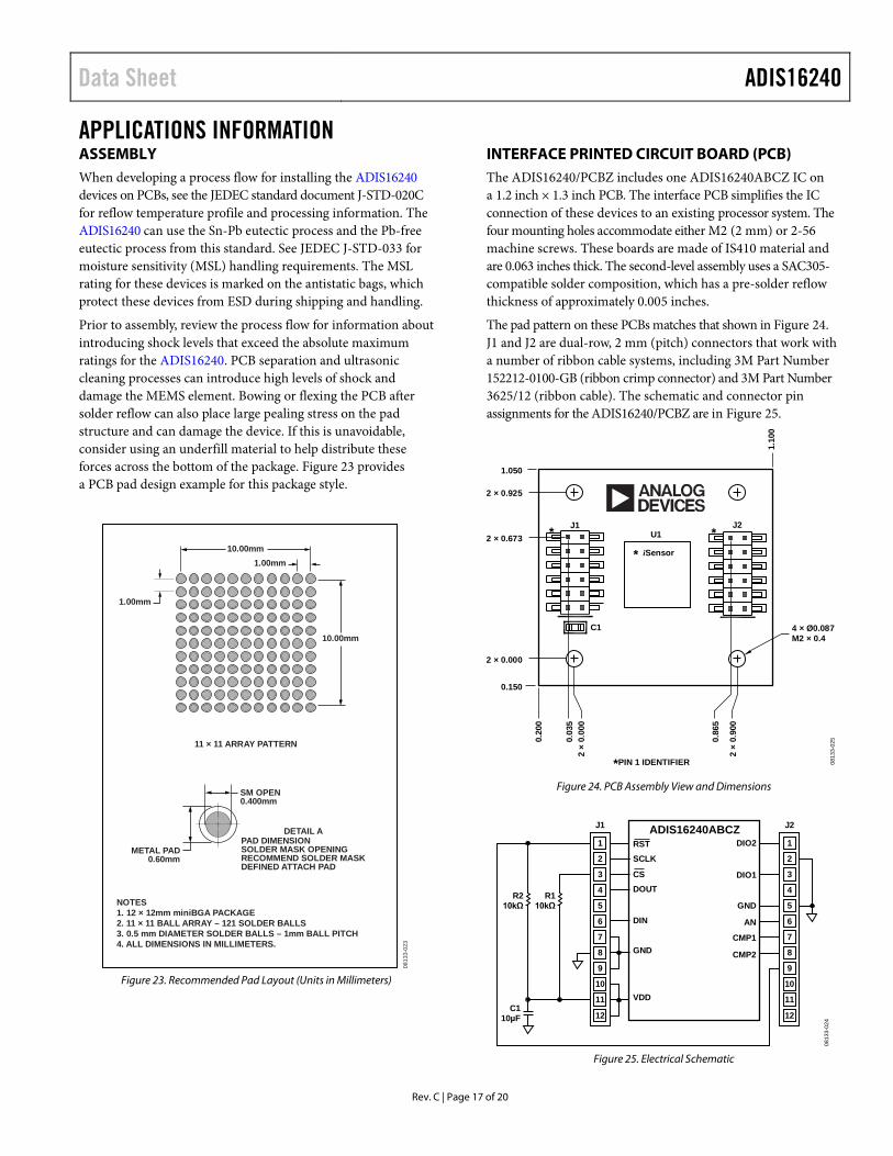
APPLICATIONS INFORMATION ASSEMBLY When developing a process flow for installing the ADIS16240 devices on PCBs, see the JEDEC standard document J-STD-020C for reflow temperature profile and processing information. The ADIS16240 can use the Sn-Pb eutectic process and the Pb-free eutectic process from this standard. See JEDEC J-STD-033 for moisture sensitivity (MSL) handling requirements. The MSL rating for these devices is marked on the antistatic bags, which protect these devices from ESD during shipping and handling.
Prior to assembly, review the process flow for information about introducing shock levels that exceed the absolute maximum ratings for the ADIS16240. PCB separation and ultrasonic cleaning processes can introduce high levels of shock and damage the MEMS element. Bowing or flexing the PCB after solder reflow can also place large pealing stress on the pad structure and can damage the device. If this is unavoidable, consider using an underfill material to help distribute these forces across the bottom of the package. Figure 23 provides a PCB pad design example for this package style.
0813
3-02
3
NOTES1. 12 × 12mm miniBGA PACKAGE2. 11 × 11 BALL ARRAY – 121 SOLDER BALLS3. 0.5 mm DIAMETER SOLDER BALLS – 1mm BALL PITCH4. ALL DIMENSIONS IN MILLIMETERS.
1.00mm
1.00mm
10.00mm
10.00mm
11 × 11 ARRAY PATTERN
METAL PAD0.60mm
SM OPEN0.400mm
DETAIL APAD DIMENSIONSOLDER MASK OPENINGRECOMMEND SOLDER MASKDEFINED ATTACH PAD
Figure 23. Recommended Pad Layout (Units in Millimeters)
INTERFACE PRINTED CIRCUIT BOARD (PCB) The ADIS16240/PCBZ includes one ADIS16240ABCZ IC on a 1.2 inch × 1.3 inch PCB. The interface PCB simplifies the IC connection of these devices to an existing processor system. The four mounting holes accommodate either M2 (2 mm) or 2-56 machine screws. These boards are made of IS410 material and are 0.063 inches thick. The second-level assembly uses a SAC305- compatible solder composition, which has a pre-solder reflow thickness of approximately 0.005 inches.
The pad pattern on these PCBs matches that shown in Figure 24. J1 and J2 are dual-row, 2 mm (pitch) connectors that work with a number of ribbon cable systems, including 3M Part Number 152212-0100-GB (ribbon crimp connector) and 3M Part Number 3625/12 (ribbon cable). The schematic and connector pin assignments for the ADIS16240/PCBZ are in Figure 25.
iSensor
U1J1
C1
J2
1.050
2 × 0.925
2 × 0.673
2 × 0.000
0.150
0.20
0
0.03
52
× 0.
000
0.86
5
2 ×
0.90
0
1.10
0
4 × Ø0.087M2 × 0.4
0813
3-02
5
*PIN 1 IDENTIFIER
**
*
Figure 24. PCB Assembly View and Dimensions
0813
3-02
4ADIS16240ABCZ
RST DIO2
DIO1
R210kΩ
C110µF
R110kΩ
AN
GND
CMP1
CMP2
SCLK
CSDOUT
DIN
GND
VDD
1
J2
2
3
4
5
6
7
8
9
10
11
12
1
J1
2
3
4
5
6
7
8
9
10
11
12
Figure 25. Electrical Schematic
ADIS16240 Data Sheet
Rev. C | Page 18 of 20
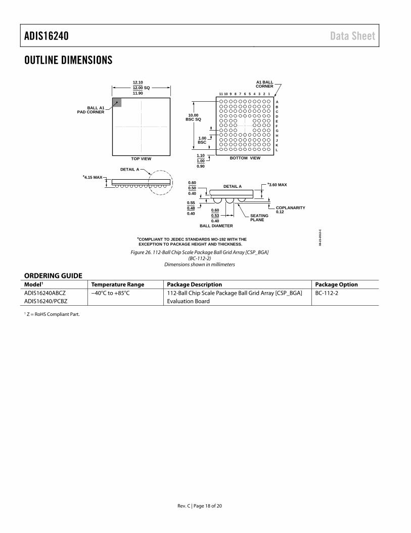
OUTLINE DIMENSIONS
08-2
3-20
12-C
A1 BALLCORNER
TOP VIEW
BALL A1PAD CORNER
DETAIL A
BOTTOM VIEW
SEATINGPLANE
BALL DIAMETER
0.600.530.40
COPLANARITY0.12
*4.15 MAX*3.60 MAX
0.550.480.40
0.600.500.40
1.101.000.90
1.00BSC
10.00BSC SQ
DETAIL A
1011 8 7 6 3 2 19 5 4
ABCDEFG
JH
KL
12.1012.00 SQ11.90
*COMPLIANT TO JEDEC STANDARDS MO-192 WITH THEEXCEPTION TO PACKAGE HEIGHT AND THICKNESS.
Figure 26. 112-Ball Chip Scale Package Ball Grid Array [CSP_BGA] (BC-112-2)
Dimensions shown in millimeters
ORDERING GUIDE Model1 Temperature Range Package Description Package Option ADIS16240ABCZ −40°C to +85°C 112-Ball Chip Scale Package Ball Grid Array [CSP_BGA] BC-112-2 ADIS16240/PCBZ Evaluation Board 1 Z = RoHS Compliant Part.

Data Sheet ADIS16240
Rev. C | Page 19 of 20
NOTES

ADIS16240 Data Sheet
Rev. C | Page 20 of 20
NOTES
©2009–2012 Analog Devices, Inc. All rights reserved. Trademarks and registered trademarks are the property of their respective owners. D08133-0-12/12(C)


![Final MSR Rev[1]. C](https://img.pdfslide.us/doc/110x75/55cf9a82550346d033a2162f/final-msr-rev1-c.jpg)