Embed Size (px)
Citation preview
2.5 Ω CMOS Low Power Dual 2:1 Mux/Demux USB 1.1 Switch
ADG787
Rev. 0 Information furnished by Analog Devices is believed to be accurate and reliable. However, no responsibility is assumed by Analog Devices for its use, nor for any infringements of patents or other rights of third parties that may result from its use. Specifications subject to change without notice. No license is granted by implication or otherwise under any patent or patent rights of Analog Devices. Trademarks and registered trademarks are the property of their respective owners.
One Technology Way, P.O. Box 9106, Norwood, MA 02062-9106, U.S.A. Tel: 781.329.4700 www.analog.com Fax: 781.326.8703 © 2005 Analog Devices, Inc. All rights reserved.
FEATURES
USB 1.1 signal switching compliant −3 dB bandwidth 150 MHz Tiny 10-lead LFCSP, WLCSP, MSOP packages Single-supply 1.8 V to 5.5 V operation Low on resistance
2.5 Ω typ 3.35 max at 85°C
Typical power consumption: <0.1 µW
APPLICATIONS
USB 1.1 signal switching circuits Cellular phones PDAs MP3 players Battery-powered systems Headphone switching Audio and video signal routing Communications systems
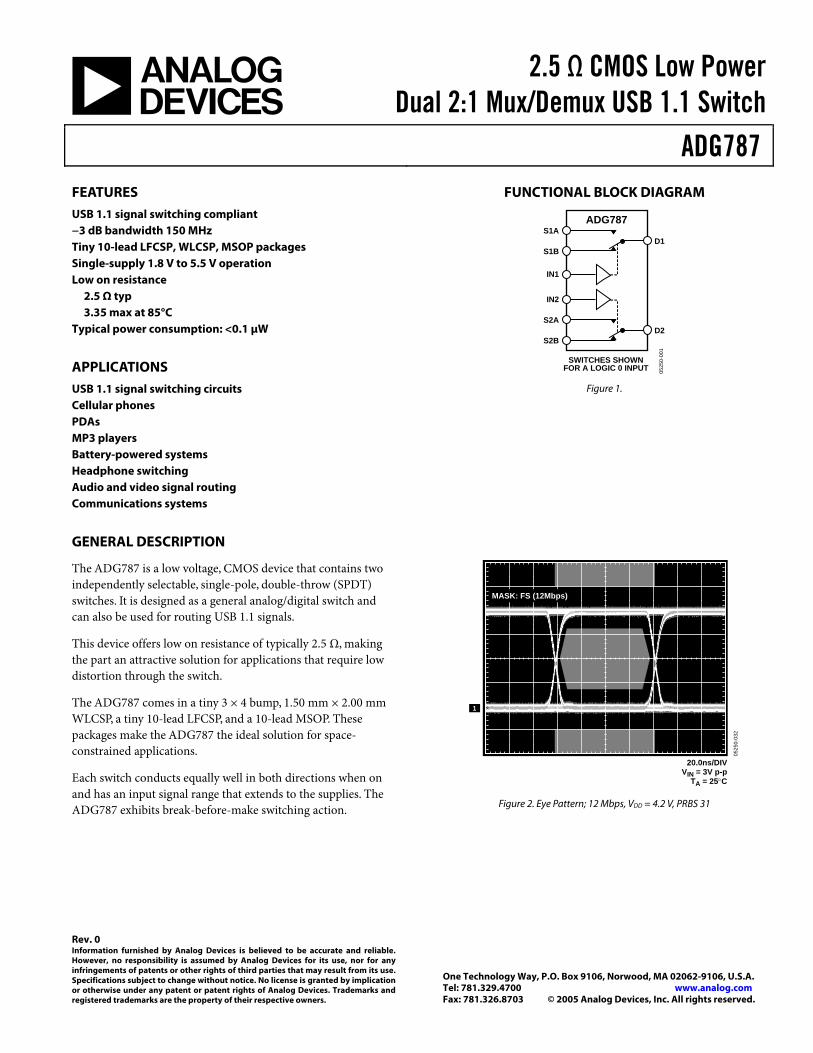
FUNCTIONAL BLOCK DIAGRAM
0525
0-00
1
SWITCHES SHOWNFOR A LOGIC 0 INPUT
ADG787S1A
S1BD1
IN1
S2A
S2BD2
IN2
Figure 1.
GENERAL DESCRIPTION
The ADG787 is a low voltage, CMOS device that contains two independently selectable, single-pole, double-throw (SPDT) switches. It is designed as a general analog/digital switch and can also be used for routing USB 1.1 signals.
This device offers low on resistance of typically 2.5 Ω, making the part an attractive solution for applications that require low distortion through the switch.
The ADG787 comes in a tiny 3 × 4 bump, 1.50 mm × 2.00 mm WLCSP, a tiny 10-lead LFCSP, and a 10-lead MSOP. These packages make the ADG787 the ideal solution for space-constrained applications.
Each switch conducts equally well in both directions when on and has an input signal range that extends to the supplies. The ADG787 exhibits break-before-make switching action.
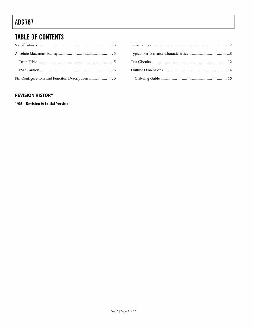
0525
0-03
2
1
20.0ns/DIVVIN = 3V p-p
TA = 25°C
MASK: FS (12Mbps)
Figure 2. Eye Pattern; 12 Mbps, VDD = 4.2 V, PRBS 31
ADG787
Rev. 0 | Page 2 of 16
TABLE OF CONTENTS Specifications..................................................................................... 3
Absolute Maximum Ratings............................................................ 5
Truth Table .................................................................................... 5
ESD Caution.................................................................................. 5
Pin Configurations and Function Descriptions ........................... 6
Terminology .......................................................................................7
Typical Performance Characteristics ..............................................8
Test Circuits..................................................................................... 12
Outline Dimensions ....................................................................... 14
Ordering Guide .......................................................................... 15
REVISION HISTORY
1/05—Revision 0: Initial Version
ADG787
Rev. 0 | Page 3 of 16
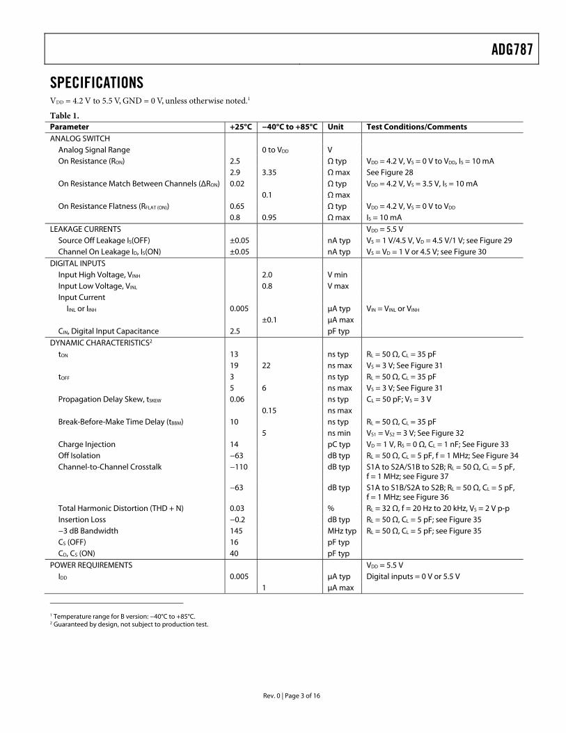
SPECIFICATIONS VDD = 4.2 V to 5.5 V, GND = 0 V, unless otherwise noted.1
Table 1. Parameter +25°C −40°C to +85°C Unit Test Conditions/Comments ANALOG SWITCH
Analog Signal Range 0 to VDD V On Resistance (RON) 2.5 Ω typ VDD = 4.2 V, VS = 0 V to VDD, IS = 10 mA 2.9 3.35 Ω max See Figure 28 On Resistance Match Between Channels (∆RON) 0.02 Ω typ VDD = 4.2 V, VS = 3.5 V, IS = 10 mA
0.1 Ω max On Resistance Flatness (RFLAT (ON)) 0.65 Ω typ VDD = 4.2 V, VS = 0 V to VDD
0.8 0.95 Ω max IS = 10 mA LEAKAGE CURRENTS VDD = 5.5 V
Source Off Leakage IS(OFF) ±0.05 nA typ VS = 1 V/4.5 V, VD = 4.5 V/1 V; see Figure 29 Channel On Leakage ID, IS(ON) ±0.05 nA typ VS = VD = 1 V or 4.5 V; see Figure 30
DIGITAL INPUTS Input High Voltage, VINH 2.0 V min Input Low Voltage, VINL 0.8 V max Input Current
IINL or IINH 0.005 µA typ VIN = VINL or VINH
±0.1 µA max CIN, Digital Input Capacitance 2.5 pF typ
DYNAMIC CHARACTERISTICS2 tON 13 ns typ RL = 50 Ω, CL = 35 pF 19 22 ns max VS = 3 V; See Figure 31 tOFF 3 ns typ RL = 50 Ω, CL = 35 pF 5 6 ns max VS = 3 V; See Figure 31 Propagation Delay Skew, tSKEW 0.06 ns typ CL = 50 pF; VS = 3 V 0.15 ns max Break-Before-Make Time Delay (tBBM) 10 ns typ RL = 50 Ω, CL = 35 pF 5 ns min VS1 = VS2 = 3 V; See Figure 32 Charge Injection 14 pC typ VD = 1 V, RS = 0 Ω, CL = 1 nF; See Figure 33 Off Isolation −63 dB typ RL = 50 Ω, CL = 5 pF, f = 1 MHz; See Figure 34 Channel-to-Channel Crosstalk −110 dB typ S1A to S2A/S1B to S2B; RL = 50 Ω, CL = 5 pF,
f = 1 MHz; see Figure 37 −63 dB typ S1A to S1B/S2A to S2B; RL = 50 Ω, CL = 5 pF,
f = 1 MHz; see Figure 36 Total Harmonic Distortion (THD + N) 0.03 % RL = 32 Ω, f = 20 Hz to 20 kHz, VS = 2 V p-p Insertion Loss −0.2 dB typ RL = 50 Ω, CL = 5 pF; see Figure 35 −3 dB Bandwidth 145 MHz typ RL = 50 Ω, CL = 5 pF; see Figure 35 CS (OFF) 16 pF typ CD, CS (ON) 40 pF typ
POWER REQUIREMENTS VDD = 5.5 V IDD 0.005 µA typ Digital inputs = 0 V or 5.5 V 1 µA max
1 Temperature range for B version: −40°C to +85°C. 2 Guaranteed by design, not subject to production test.
ADG787
Rev. 0 | Page 4 of 16
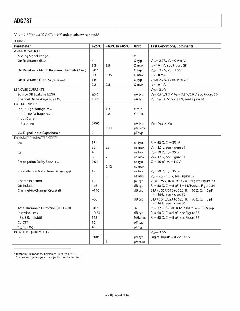
VDD = 2.7 V to 3.6 V, GND = 0 V, unless otherwise noted.1
Table 2. Parameter +25°C −40°C to +85°C Unit Test Conditions/Comments ANALOG SWITCH
Analog Signal Range V On Resistance (RON) 4 Ω typ VDD = 2.7 V, VS = 0 V to VDD 5.2 5.5 Ω max IS = 10 mA; see Figure 28 On Resistance Match Between Channels (∆RON) 0.07 Ω typ VDD = 2.7 V, VS = 1.5 V 0.3 0.35 Ω max IS = 10 mA On Resistance Flatness (RFLAT (ON)) 1.6 Ω typ VDD = 2.7 V, VS = 0 V to VDD
2.2 2.5 Ω max IS = 10 mA LEAKAGE CURRENTS VDD = 3.6 V
Source Off Leakage IS(OFF) ±0.01 nA typ VS = 0.6 V/3.3 V, VD = 3.3 V/0.6 V; see Figure 29 Channel On Leakage ID, IS(ON) ±0.01 nA typ VS = VD = 0.6 V or 3.3 V; see Figure 30
DIGITAL INPUTS Input High Voltage, VINH 1.3 V min Input Low Voltage, VINL 0.8 V max Input Current
IINL or IINH 0.005 µA typ VIN = VINL or VINH
±0.1 µA max CIN, Digital Input Capacitance 2 pF typ
DYNAMIC CHARACTERISTICS2 tON 18 ns typ RL = 50 Ω, CL = 35 pF 30 35 ns max VS = 1.5 V; see Figure 31 tOFF 4 ns typ RL = 50 Ω, CL = 35 pF 6 7 ns max VS = 1.5 V; see Figure 31 Propagation Delay Skew, tSKEW 0.04 ns typ CL = 50 pF; VS = 1.5 V 0.12 ns max Break-Before-Make Time Delay (tBBM) 15 ns typ RL = 50 Ω, CL = 35 pF 5 ns min VS1 = VS2 = 1.5 V; see Figure 32 Charge Injection 10 pC typ VD = 1.25 V, RS = 0 Ω, CL = 1 nF; see Figure 33 Off Isolation −63 dB typ RL = 50 Ω, CL = 5 pF, f = 1 MHz; see Figure 34 Channel-to-Channel Crosstalk −110 dB typ S1A to S2A/S1B to S2B; RL = 50 Ω, CL = 5 pF,
f = 1 MHz; see Figure 37 −63 dB typ S1A to S1B/S2A to S2B; RL = 50 Ω, CL = 5 pF,
f = 1 MHz; see Figure 35 Total Harmonic Distortion (THD + N) 0.07 % RL = 32 Ω, f = 20 Hz to 20 kHz, VS = 1.5 V p-p Insertion Loss −0.24 dB typ RL = 50 Ω, CL = 5 pF; see Figure 35 −3 dB Bandwidth 145 MHz typ RL = 50 Ω, CL = 5 pF; see Figure 35 CS (OFF) 16 pF typ CD, CS (ON) 40 pF typ
POWER REQUIREMENTS VDD = 3.6 V IDD 0.005 µA typ Digital Inputs = 0 V or 3.6 V
1 µA max
1 Temperature range for B version: −40°C to +85°C. 2 Guaranteed by design, not subject to production test.
ADG787
Rev. 0 | Page 5 of 16
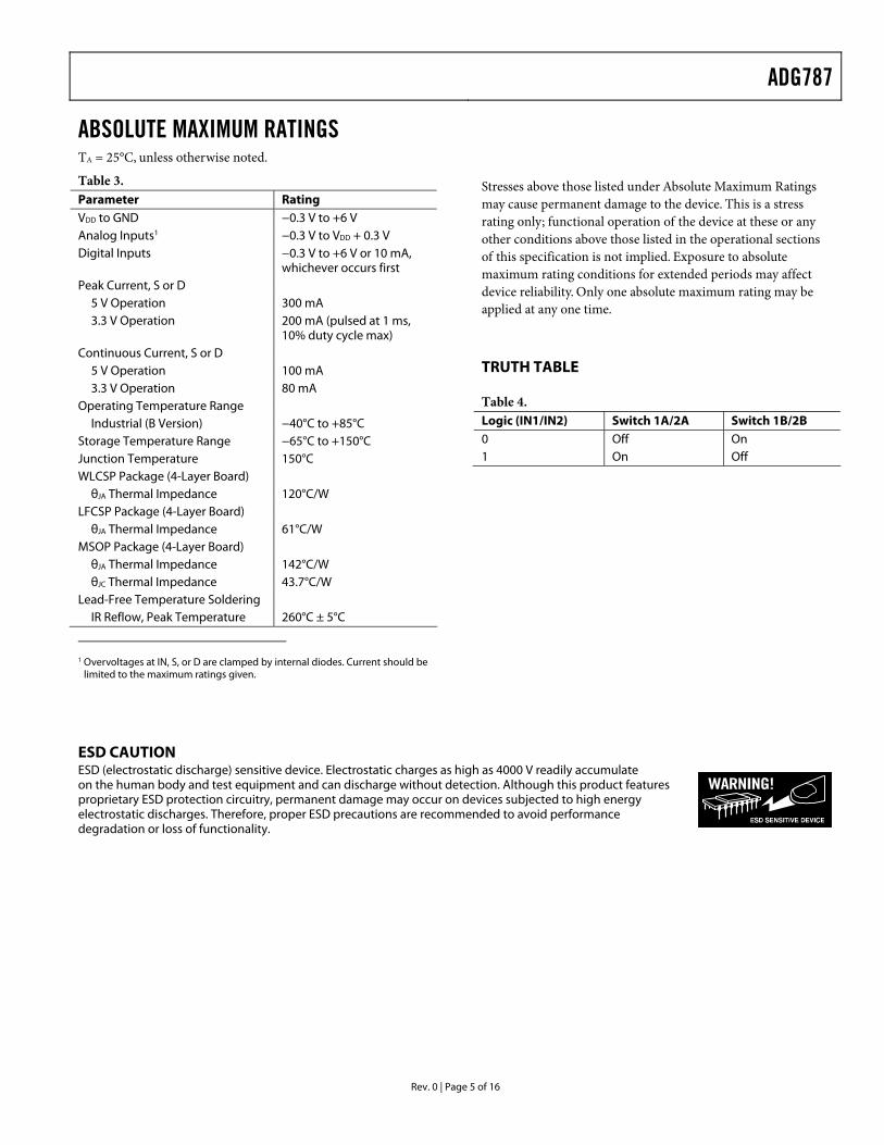
ABSOLUTE MAXIMUM RATINGSTA = 25°C, unless otherwise noted.
Table 3. Parameter Rating VDD to GND −0.3 V to +6 V Analog Inputs1 −0.3 V to VDD + 0.3 V Digital Inputs1 −0.3 V to +6 V or 10 mA,
whichever occurs first Peak Current, S or D
5 V Operation 300 mA 3.3 V Operation 200 mA (pulsed at 1 ms,
10% duty cycle max) Continuous Current, S or D
5 V Operation 100 mA 3.3 V Operation 80 mA
Operating Temperature Range Industrial (B Version) −40°C to +85°C
Storage Temperature Range −65°C to +150°C Junction Temperature 150°C WLCSP Package (4-Layer Board)
θJA Thermal Impedance 120°C/W LFCSP Package (4-Layer Board)
θJA Thermal Impedance 61°C/W MSOP Package (4-Layer Board)
θJA Thermal Impedance 142°C/W θJC Thermal Impedance 43.7°C/W
Lead-Free Temperature Soldering IR Reflow, Peak Temperature 260°C ± 5°C
1 Overvoltages at IN, S, or D are clamped by internal diodes. Current should be
limited to the maximum ratings given.
Stresses above those listed under Absolute Maximum Ratings may cause permanent damage to the device. This is a stress rating only; functional operation of the device at these or any other conditions above those listed in the operational sections of this specification is not implied. Exposure to absolute maximum rating conditions for extended periods may affect device reliability. Only one absolute maximum rating may be applied at any one time.
TRUTH TABLE Table 4. Logic (IN1/IN2) Switch 1A/2A Switch 1B/2B 0 Off On 1 On Off
ESD CAUTION ESD (electrostatic discharge) sensitive device. Electrostatic charges as high as 4000 V readily accumulate on the human body and test equipment and can discharge without detection. Although this product features proprietary ESD protection circuitry, permanent damage may occur on devices subjected to high energy electrostatic discharges. Therefore, proper ESD precautions are recommended to avoid performance degradation or loss of functionality.
ADG787
Rev. 0 | Page 6 of 16
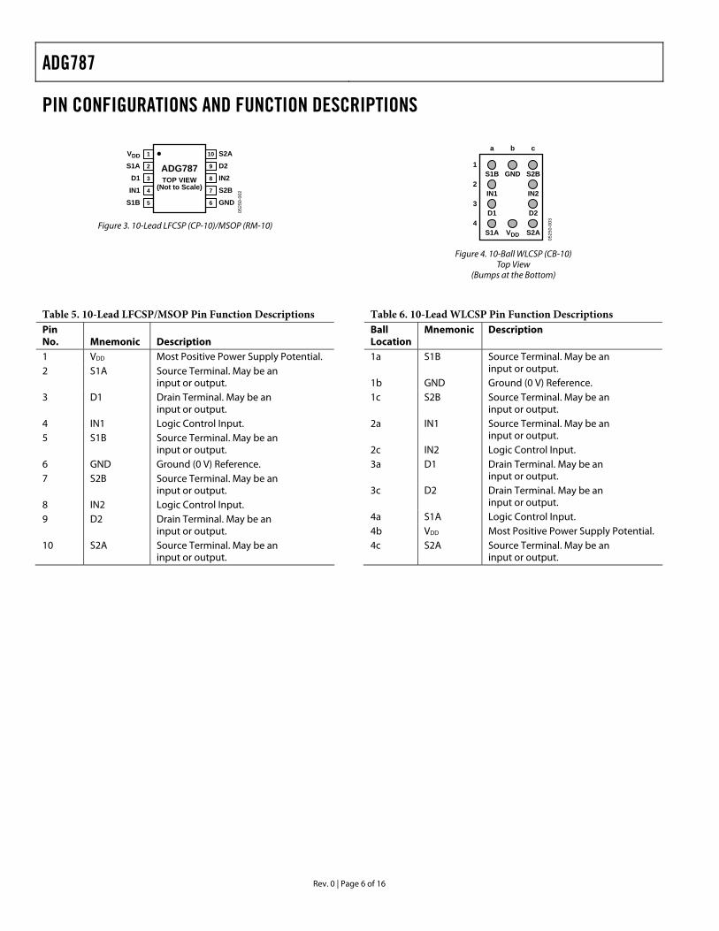
PIN CONFIGURATIONS AND FUNCTION DESCRIPTIONS
0525
0-00
2
ADG787TOP VIEW
(Not to Scale)
VDD 1
S1A 2
D1 3
IN1 4
S1B 5
S2AD2IN2S2BGND
10
9
8
7
6
Figure 3. 10-Lead LFCSP (CP-10)/MSOP (RM-10)
0525
0-00
3
S2BGNDS1B
a b c
IN2IN1
D2D1
S2A
1
2
3
4VDDS1A
Figure 4. 10-Ball WLCSP (CB-10) Top View
(Bumps at the Bottom)
Table 5. 10-Lead LFCSP/MSOP Pin Function Descriptions Pin No. Mnemonic Description 1 VDD Most Positive Power Supply Potential. 2 S1A Source Terminal. May be an
input or output. 3 D1 Drain Terminal. May be an
input or output. 4 IN1 Logic Control Input. 5 S1B Source Terminal. May be an
input or output. 6 GND Ground (0 V) Reference. 7 S2B Source Terminal. May be an
input or output. 8 IN2 Logic Control Input. 9 D2 Drain Terminal. May be an
input or output. 10 S2A Source Terminal. May be an
input or output.
Table 6. 10-Lead WLCSP Pin Function Descriptions Ball Location
Mnemonic Description
1a S1B Source Terminal. May be an input or output.
1b GND Ground (0 V) Reference. 1c S2B Source Terminal. May be an
input or output. 2a IN1 Source Terminal. May be an
input or output. 2c IN2 Logic Control Input. 3a D1 Drain Terminal. May be an
input or output. 3c D2 Drain Terminal. May be an
input or output. 4a S1A Logic Control Input. 4b VDD Most Positive Power Supply Potential. 4c S2A Source Terminal. May be an
input or output.
ADG787
Rev. 0 | Page 7 of 16
TERMINOLOGY
IDD
Positive supply current.
VD (VS) Analog voltage on terminals D and S.
RON
Ohmic resistance between D and S.
RFLAT (ON) Flatness is defined as the difference between the maximum and minimum value of on resistance as measured
ΔRON
On resistance match between any two channels.
IS (OFF) Source leakage current with the switch off.
ID (OFF) Drain leakage current with the switch off.
ID, IS (ON) Channel leakage current with the switch on.
VINL
Maximum input voltage for Logic 0.
VINH
Minimum input voltage for Logic 1.
IINL (IINH) Input current of the digital input.
CS (OFF) Off switch source capacitance. Measured with reference to ground.
CD (OFF) Off switch drain capacitance. Measured with reference to ground.
CD, CS (ON) On switch capacitance. Measured with reference to ground.
CIN
Digital input capacitance.
tON
Delay time between the 50% and the 90% points of the digital input and switch on condition.
tOFF
Delay time between the 50% and the 90% points of the digital input and switch off condition.
tBBM
On or off time measured between the 80% points of both switches when switching from one to another.
Charge Injection A measure of the glitch impulse transferred from the digital input to the analog output during on-off switching.
Off Isolation A measure of unwanted signal coupling through an off switch.
Crosstalk A measure of unwanted signal that is coupled from one channel to another as a result of parasitic capacitance.
−3 dB Bandwidth The frequency at which the output is attenuated by 3 dB.
On Response The frequency response of the on switch.
Insertion Loss The loss due to the on resistance of the switch.
THD + N The ratio of the harmonic amplitudes plus noise of a signal, to the fundamental.
TSKEW The measure of the variation in propagation delay between each channel.
Rise Time Delay The rise time of a signal is a measure of the time for the signal to rise from 10% of the ON level to 90% of the ON level. Rise time delay is the difference between the rise time, measured at the input, and the rise time, measured at the output.
Fall Time Delay The fall time of a signal is a measure of the time for the signal to fall from 90% of the ON level to 10% of the ON level. Fall time delay is the difference between the fall time, measured at the input, and the fall time, measured at the output.
Rise-Time-to-Fall-Time Mismatch This is the absolute value between the variation in the fall time and the rise time, measured at the output.
ADG787
Rev. 0 | Page 8 of 16
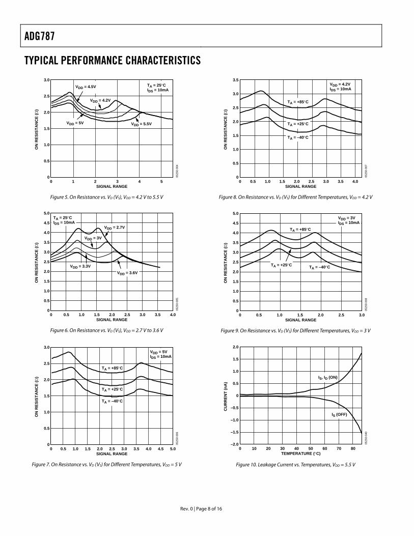
TYPICAL PERFORMANCE CHARACTERISTICS
3.0
2.5
2.0
1.5
1.0
0.5
00 1 3 52 4
0525
0-00
4
SIGNAL RANGE
ON
RES
ISTA
NC
E (Ω
)
TA = 25°CIDS = 10mA
VDD = 4.5V
VDD = 4.2V
VDD = 5V VDD = 5.5V
Figure 5. On Resistance vs. VD (VS), VDD = 4.2 V to 5.5 V
5.0
4.5
4.0
3.5
3.0
2.5
2.0
1.5
1.0
0.5
00 4.03.53.02.52.01.51.00.5
0525
0-00
5
SIGNAL RANGE
ON
RES
ISTA
NC
E (Ω
)
TA = 25°CIDS = 10mA
VDD = 3.6V
VDD = 2.7V
VDD = 3V
VDD = 3.3V
Figure 6. On Resistance vs. VD (VS), VDD = 2.7 V to 3.6 V
3.0
2.5
2.0
1.5
1.0
0.5
00 5.04.0 4.53.53.02.52.01.51.00.5
0525
0-00
6
SIGNAL RANGE
ON
RES
ISTA
NC
E (Ω
)
VDD = 5VIDS = 10mA
TA = +85°C
TA = +25°C
TA = –40°C
Figure 7. On Resistance vs. VD (VS) for Different Temperatures, VDD = 5 V
3.5
3.0
2.5
2.0
1.5
1.0
0.5
00 4.03.53.02.52.01.51.00.5
0525
0-00
7
SIGNAL RANGE
ON
RES
ISTA
NC
E (Ω
)
VDD = 4.2VIDS = 10mA
TA = +85°C
TA = +25°C
TA = –40°C
Figure 8. On Resistance vs. VD (VS) for Different Temperatures, VDD = 4.2 V
5.0
4.5
4.0
3.5
3.0
2.5
2.0
1.5
1.0
0.5
00 3.02.52.01.51.00.5
0525
0-00
8
SIGNAL RANGE
ON
RES
ISTA
NC
E (Ω
)
VDD = 3VIDS = 10mA
TA = +85°C
TA = +25°C TA = –40°C
Figure 9. On Resistance vs. VD (VS) for Different Temperatures, VDD = 3 V
2.0
1.5
1.0
0.5
0
–0.5
–1.0
–1.5
–2.00 870605040302010
0525
0-04
0
TEMPERATURE (°C)
CU
RR
ENT
(nA
)
0
IS, ID (ON)
IS (OFF)
Figure 10. Leakage Current vs. Temperatures, VDD = 5.5 V
ADG787
Rev. 0 | Page 9 of 16
0
2.0
1.5
1.0
0.5
0
–0.5
–1.0
–1.5
–2.00 870605040302010
0525
0-04
1
TEMPERATURE (°C)
CU
RR
ENT
(nA
)
IS (OFF)
IS, ID (ON)
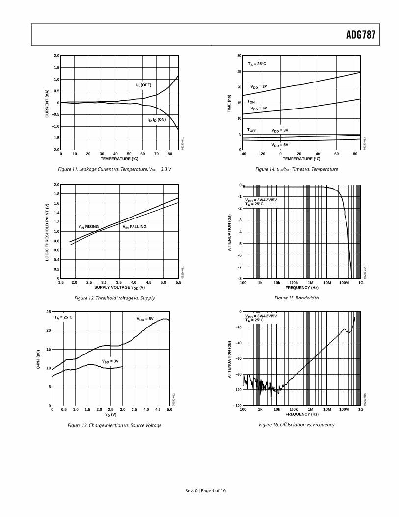
Figure 11. Leakage Current vs. Temperature, VDD = 3.3 V
2.0
1.8
1.6
1.4
1.2
1.0
0.8
0.6
0.4
0.2
01.5 5.55.04.54.03.53.02.52.0
0525
0-01
1
SUPPLY VOLTAGE VDD (V)
LOG
IC T
HR
ESH
OLD
PO
INT
(V)
VIN RISING VIN FALLING
Figure 12. Threshold Voltage vs. Supply
25
20
15
10
5
00 5.03.0 3.5 4.0 4.52.52.01.51.00.5
0525
0-01
2
VD (V)
Q-IN
J (p
C)
TA = 25°C VDD = 5V
VDD = 3V
Figure 13. Charge Injection vs. Source Voltage
30
25
20
15
10
5
0–40 806040200–20
0525
0-01
3
TEMPERATURE (°C)
TIM
E (n
s)
TOFF
TA = 25°C
VDD = 3V
VDD = 5V
VDD = 5V
VDD = 3V
TON
Figure 14. tON/tOFF Times vs. Temperature
0
–1
–2
–3
–4
–5
–6
–7
–8100 1k 10k 100k 1M 10M 100M 1G
0525
0-01
4
FREQUENCY (Hz)
ATT
ENU
ATI
ON
(dB
)
VDD = 3V/4.2V/5VTA = 25°C
Figure 15. Bandwidth
0
–120
–100
–80
–60
–40
–20
100 1k 10k 100k 1M 10M 100M 1G
0525
0-01
5
FREQUENCY (Hz)
ATT
ENU
ATI
ON
(dB
)
VDD = 3V/4.2V/5VTA = 25°C
Figure 16. Off Isolation vs. Frequency
ADG787
Rev. 0 | Page 10 of 16
0
–120
–100
–80
–60
–40
–20
100 1k 10k 100k 1M 10M 100M 1G
0525
0-03
0
FREQUENCY (Hz)
ATT
ENU
ATI
ON
(dB
)
VDD = 3V/4.2V/5VTA = 25°C
S1A–S1B
S1A–S2A
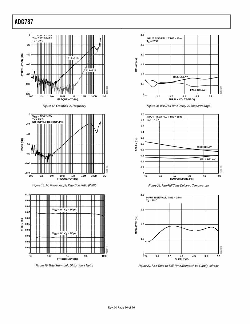
Figure 17. Crosstalk vs. Frequency
0
–120
–100
–80
–60
–40
–20
100 1k 10k 100k 1M 10M 100M 1G
0525
0-03
1
FREQUENCY (Hz)
PSR
R (d
B)
VDD = 3V/4.2V/5VTA = 25°CNO SUPPLY DECOUPLING
Figure 18. AC Power Supply Rejection Ratio (PSRR)
0.10
0.09
0.08
0.07
0.06
0.05
0.04
0.03
0.02
0.01
010 100k10k100 1k
0525
0-04
3
FREQUENCY (Hz)
THD
+N (%
)
VDD = 3V, VS = 2V p-p
VDD = 5V, VS = 2V p-p
Figure 19. Total Harmonic Distortion + Noise
3.0
2.5
2.0
1.5
1.0
0.5
02.7 5.24.74.23.2 3.7
0525
0-04
4
SUPPLY VOLTAGE (V)
DEL
AY
(ns)
INPUT RISE/FALL TIME = 15nsTA = 25°C
FALL DELAY
RISE DELAY
Figure 20. Rise/Fall Time Delay vs. Supply Voltage
2.0
1.8
1.6
1.4
1.2
1.0
0.8
0.6
0.4
0.2
0–40 856035–15 10
0525
0-04
5
TEMPERATURE (°C)
DEL
AY
(ns)
INPUT RISE/FALL TIME = 15nsVDD = 4.2V
RISE DELAY
FALL DELAY
Figure 21. Rise/Fall Time Delay vs. Temperature
2.0
1.5
1.0
0.5
02.5 3.0 5.55.04.53.5 4.0
0525
0-04
6
SUPPLY (V)
MIS
MA
TCH
(ns)
INPUT RISE/FALL TIME = 15nsTA = 25°C
Figure 22. Rise-Time-to-Fall-Time Mismatch vs. Supply Voltage
ADG787
Rev. 0 | Page 11 of 16
1.2
1.0
0.8
0.6
0.4
0.2
0–40 –15 10 35 60 85
0525
0-04
7
TEMPERATURE (°C)
MIS
MA
TCH
(ns)
INPUT RISE/FALL TIME = 15nsVDD = 4.2V
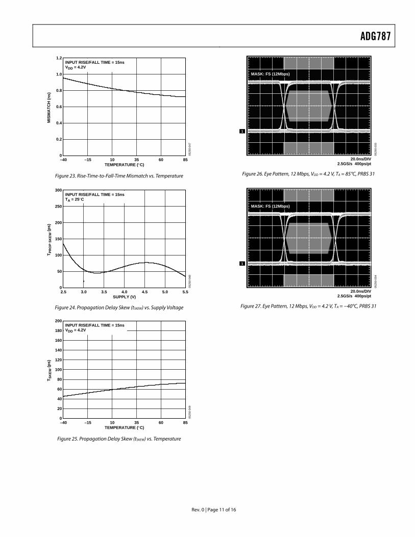
Figure 23. Rise-Time-to-Fall-Time Mismatch vs. Temperature
300
250
200
150
100
50
02.5 3.0 3.5 4.0 4.5 5.0 5.5
0525
0-04
8
SUPPLY (V)
T PR
OP
SKEW
(ps)
INPUT RISE/FALL TIME = 15nsTA = 25°C
Figure 24. Propagation Delay Skew (tSKEW) vs. Supply Voltage
200
180
160
140
120
100
80
60
40
20
0–40 –15 10 35 60 85
0525
0-04
9
TEMPERATURE (°C)
T SK
EW (p
s)
INPUT RISE/FALL TIME = 15nsVDD = 4.2V
Figure 25. Propagation Delay Skew (tSKEW) vs. Temperature
0525
0-03
3
1
20.0ns/DIV2.5GS/s 400ps/pt
MASK: FS (12Mbps)
Figure 26. Eye Pattern, 12 Mbps, VDD = 4.2 V, TA = 85°C, PRBS 31
0525
0-03
4
1
20.0ns/DIV2.5GS/s 400ps/pt
MASK: FS (12Mbps)
Figure 27. Eye Pattern, 12 Mbps, VDD = 4.2 V, TA = −40°C, PRBS 31
ADG787
Rev. 0 | Page 12 of 16
TEST CIRCUITS
S D
VS RON = V1/IDS
IDS
V1
0525
0-01
6
Figure 28. On Resistance
S D
VS VD
IS (OFF) ID (OFF)
A A
0525
0-01
7
Figure 29. Off Leakage
S D
VD
ID (ON)
NC A
0525
0-01
8
Figure 30. On Leakage
0525
0-01
9
D
IN
GND
RL50Ω
CL35pF
VDD
VINVOUTVS
VDD
VOUT
tON tOFF
50% 50%
90% 90%
0.1µF
S1BS1A
Figure 31. Switching Times, tON, tOFF
VOUT
VIN
tBBM tBBM
50% 50%
80%
0V
D
IN
GND
RL50Ω
CL35pF
VDD
VOUTVS
VDD
0.1µF
S1BS1A 80%
0525
0-02
0
Figure 32. Break-Before-Make Time Delay, tBBM
0525
0-02
1
IN
GND
VDD
VS
VIN
VOUT
1nF
VOUT
NC
SW ON
QINJ = CL × ∆VOUT
SW OFF
∆VOUT
S1B
S1AD
Figure 33. Charge Injection
ADG787
Rev. 0 | Page 13 of 16
0525
0-02
2
VDD
VS
VDD
NC
NETWORKANALYZER
S1B S1A
GND
OFF ISOLATION = 20 LOG
D
50Ω50Ω
VOUTRL50Ω
0.1µF
VOUTVS
Figure 34. Off Isolation
0525
0-02
3
VOUT
VDD
VDD
GNDVS
RL50Ω
RL50Ω
0.1µF
50Ω
S1A
DS1B
CHANNEL-TO-CHANNEL CROSSTALK = 20 LOGVOUTVS
Figure 35. Channel-to-Channel Crosstalk (S1A to S1B)
NETWORKANALYZER
RL
GND
VDD
VDD
VOUT
VSS1AS1B
0.1µF
D
50Ω
50Ω
INSERTION LOSS = 20 LOGVOUT WITH SWITCH
VOUT WITHOUT SWITCH
0525
0-02
4
Figure 36. Bandwidth
0525
0-02
5
VOUT50Ω
50Ω50ΩVS
NETWORKANALYZER
S2A
S2B
D1
D2NC
NC
S1A
S1B
CHANNEL-TO-CHANNEL CROSSTALK = 20 LOGVOUTVS
Figure 37. Channel-to-Channel Crosstalk (S1A to S2A)
ADG787
Rev. 0 | Page 14 of 16
OUTLINE DIMENSIONS
3.00BSC SQ
INDEXAREA
TOP VIEW
1.50BCS SQ
EXPOSEDPAD
(BOTTOM VIEW)
1.741.641.49
2.482.382.23
1
6
10
0.50BSC
0.500.400.30
5
PIN 1INDICATOR
0.800.750.70 0.05 MAX
0.02 NOM
SEATINGPLANE 0.30
0.230.18
0.20 REF
0.80 MAX0.55 TYP
SIDE VIEW
Figure 38. 10-Lead Lead Frame Chip Scale Package [WD_LFCSP] 3 mm × 3 mm Body, Very, Very Thin, Dual Lead (CP-10-9)
Dimensions shown in millimeters
0.230.08
0.800.600.40
8°0°
0.150.00
0.270.17
0.950.850.75
SEATINGPLANE
1.10 MAX
10 6
51
0.50 BSC
3.00 BSC
3.00 BSC
4.90 BSC
PIN 1
COPLANARITY0.10
COMPLIANT TO JEDEC STANDARDS MO-187BA
Figure 39. 10-Lead Mini Small Outline Package [MSOP] (RM-10)
Dimensions shown in millimeters
SEATINGPLANE
0.50 BSCBALL PITCH
1.561.501.44
0.260.220.18
0.110.090.07
0.360.320.28
0.630.570.51
BOTTOMVIEW
2.062.001.94
TOP VIEW(BALL SIDE DOWN)
1
ABC
2
3
4
BUMP 1IDENTIFIER
Figure 40. 10-Ball Wafer Level Chip Scale Package [WLCSP] (CB-10)
Dimensions shown in millimeters
ADG787
Rev. 0 | Page 15 of 16
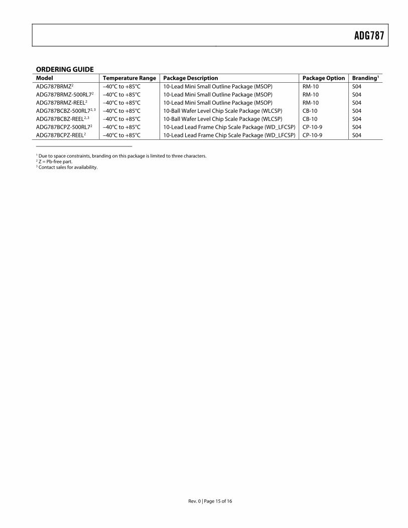
ORDERING GUIDE Model Temperature Range Package Description Package Option Branding1
ADG787BRMZ2 –40°C to +85°C 10-Lead Mini Small Outline Package (MSOP) RM-10 S04 ADG787BRMZ-500RL72 –40°C to +85°C 10-Lead Mini Small Outline Package (MSOP) RM-10 S04 ADG787BRMZ-REEL2 –40°C to +85°C 10-Lead Mini Small Outline Package (MSOP) RM-10 S04 ADG787BCBZ-500RL72, 3 –40°C to +85°C 10-Ball Wafer Level Chip Scale Package (WLCSP) CB-10 S04 ADG787BCBZ-REEL2,.3 –40°C to +85°C 10-Ball Wafer Level Chip Scale Package (WLCSP) CB-10 S04 ADG787BCPZ-500RL72 –40°C to +85°C 10-Lead Lead Frame Chip Scale Package (WD_LFCSP) CP-10-9 S04 ADG787BCPZ-REEL2 –40°C to +85°C 10-Lead Lead Frame Chip Scale Package (WD_LFCSP) CP-10-9 S04
1 Due to space constraints, branding on this package is limited to three characters.2 Z = Pb-free part. 3 Contact sales for availability.
ADG787
Rev. 0 | Page 16 of 16
NOTES
© 2005 Analog Devices, Inc. All rights reserved. Trademarks and registered trademarks are the property of their respective owners. D05250–0–1/05(0)