Embed Size (px)
Citation preview
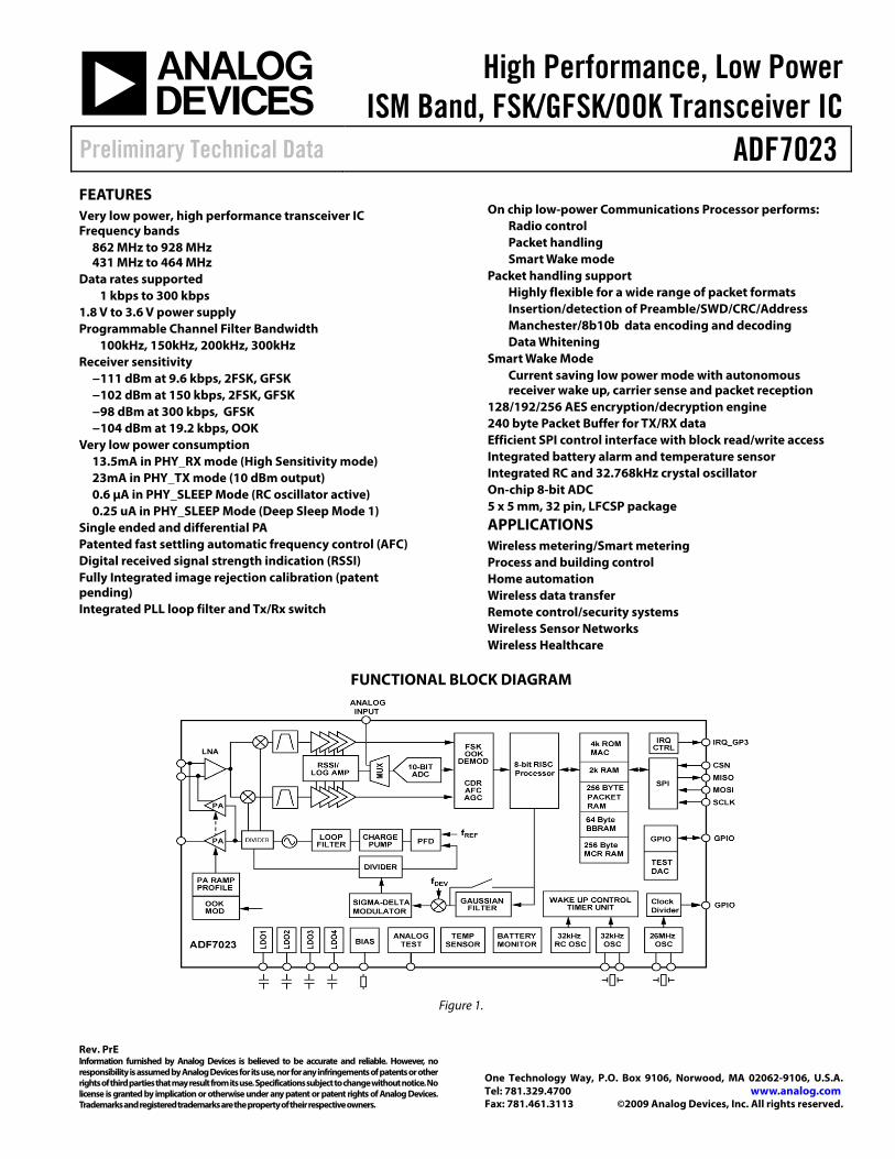
High Performance, Low PowerISM Band, FSK/GFSK/OOK Transceiver IC
Preliminary Technical Data ADF7023
Rev. PrE Information furnished by Analog Devices is believed to be accurate and reliable. However, no responsibility is assumed by Analog Devices for its use, nor for any infringements of patents or other rights of third parties that may result from its use. Specifications subject to change without notice. No license is granted by implication or otherwise under any patent or patent rights of Analog Devices. Trademarks and registered trademarks are the property of their respective owners.
One Technology Way, P.O. Box 9106, Norwood, MA 02062-9106, U.S.A.Tel: 781.329.4700 www.analog.com Fax: 781.461.3113 ©2009 Analog Devices, Inc. All rights reserved.
FEATURES Very low power, high performance transceiver IC Frequency bands
862 MHz to 928 MHz 431 MHz to 464 MHz
Data rates supported 1 kbps to 300 kbps
1.8 V to 3.6 V power supply Programmable Channel Filter Bandwidth
100kHz, 150kHz, 200kHz, 300kHz Receiver sensitivity
−111 dBm at 9.6 kbps, 2FSK, GFSK −102 dBm at 150 kbps, 2FSK, GFSK −98 dBm at 300 kbps, GFSK −104 dBm at 19.2 kbps, OOK
Very low power consumption 13.5mA in PHY_RX mode (High Sensitivity mode) 23mA in PHY_TX mode (10 dBm output) 0.6 μA in PHY_SLEEP Mode (RC oscillator active) 0.25 uA in PHY_SLEEP Mode (Deep Sleep Mode 1)
Single ended and differential PA Patented fast settling automatic frequency control (AFC) Digital received signal strength indication (RSSI) Fully Integrated image rejection calibration (patent pending) Integrated PLL loop filter and Tx/Rx switch
On chip low-power Communications Processor performs:
Radio control Packet handling Smart Wake mode
Packet handling support Highly flexible for a wide range of packet formats Insertion/detection of Preamble/SWD/CRC/Address Manchester/8b10b data encoding and decoding Data Whitening
Smart Wake Mode Current saving low power mode with autonomous
receiver wake up, carrier sense and packet reception 128/192/256 AES encryption/decryption engine 240 byte Packet Buffer for TX/RX data Efficient SPI control interface with block read/write access Integrated battery alarm and temperature sensor Integrated RC and 32.768kHz crystal oscillator On-chip 8-bit ADC 5 x 5 mm, 32 pin, LFCSP package
APPLICATIONS Wireless metering/Smart metering Process and building control Home automation Wireless data transfer Remote control/security systems Wireless Sensor Networks Wireless Healthcare
FUNCTIONAL BLOCK DIAGRAM
Figure 1.
ADF7023 Preliminary Technical Data
Rev. PrE | Page 2 of 65
TERMINOLOGY ADC Analog to digital converter
AGC Automatic gain control
AFC Automatic frequency control
Battmon Battery Monitor
BBRAM Back up battery random access memory
CRC Cyclic redundancy check
DR Data rate
FSK Two level Frequency shift keying
GFSK Two level Gaussian frequency shift keying
SWM Smart Wake Mode
MCR Modem Configuration RAM
NOP No operation
OOK On-Off Keying
PA Power amplifier
PFD Phase frequency detector
PHY Physical Layer
RCO RC Oscillator
RISC Reduced instruction set computer
RSSI Receive signal strength indicator
Rx Receive
SWD Sync word detect
Tx Transmit
VCO Voltage controlled oscillator
WUC Wake up controller
XOSC Crystal oscillator
Preliminary Technical Data ADF7023
Rev. PrE | Page 3 of 65
TABLE OF CONTENTS Features ............................................................................................... 1
Applications ....................................................................................... 1
Functional Block Diagram ............................................................... 1
Terminology ....................................................................................... 2
General Description .......................................................................... 4
RF Overview .................................................................................. 4
Low Power Features ...................................................................... 4
Communications processor ......................................................... 4
Packet Handling ............................................................................ 4
AES .................................................................................................. 4
Auxilary Features .......................................................................... 4
Specifications ..................................................................................... 5
RF and Synthesizer Specifications .............................................. 5
Transmitter Specifications ........................................................... 5
Receiver Specifications ................................................................. 6
Timing and Digital Specifications .............................................. 7
Auxilary Block Specifications ...................................................... 8
General Specifications .................................................................. 8
Timing Characteristics ................................................................... 10
Timing Diagrams ........................................................................ 10
Absolute Maximum Ratings .......................................................... 11
ESD Caution ................................................................................ 11
Pin Configuration and Function Descriptions ........................... 12
Typical Performance Characteristics ............................................ 14
SPI Interface ..................................................................................... 16
General Characteristics .............................................................. 16
Command AcCess ....................................................................... 16
Status word ................................................................................... 16
Memory Write/Read ................................................................... 17
Wake-up from PHY_SLEEP state ............................................. 19
Programming Sequence on Wake Up or After Reset ............. 19
COmms Processor Reset ............................................................ 19
Memory Map ............................................................................... 19
Radio Control .................................................................................. 21
Operational States ....................................................................... 21
Commands ................................................................................... 22
Interrupt Generation ...................................................................... 24
Interrupt Setup ............................................................................ 24
Determining the Interrupt Source ............................................ 25
Packet Handling .............................................................................. 26
Packet Format .............................................................................. 26
Receive packet Qualification ..................................................... 27
Packet RAM Structure ................................................................ 28
Data Whitening ........................................................................... 28
Manchester & 8B/10B Encoding ............................................... 29
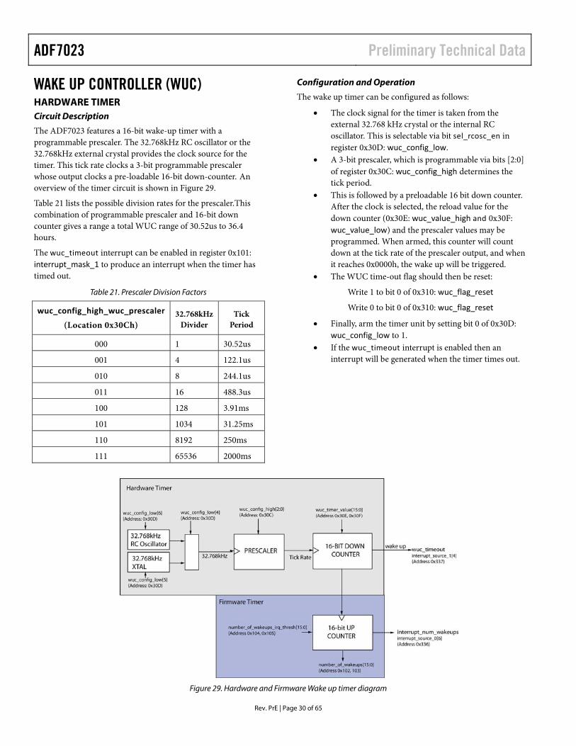
Wake Up Controller (WUC) ......................................................... 30
Hardware Timer .......................................................................... 30
Firmware timer ............................................................................ 31
Smart Wake Mode ........................................................................... 32
AES ENCRYPTION and Decryption Engine ............................. 34
Functionality ................................................................................ 34
Example Operation ..................................................................... 36
Execution times ........................................................................... 37
SPORT MODE ................................................................................ 38
Radio Blocks .................................................................................... 40
RF Frequency Generation .......................................................... 40
Modulation .................................................................................. 40
Data Rate Programming ............................................................ 40
Crystal Oscillator ........................................................................ 40
RF Output Stage .......................................................................... 40
PA/LNA Interface ........................................................................ 41
Receive Channel Filter ............................................................... 41
AutomAtIc Gain Control (AGC) .............................................. 41
Automatic Frequency Control (AFC) ...................................... 41
RSSI ............................................................................................... 42
Image RejEction calibration ...................................................... 42
Peripheral Features.......................................................................... 43
Analog To Digital Converter ..................................................... 43
Battery monitor ........................................................................... 43
Application Circuit ......................................................................... 44
Command Reference ...................................................................... 45
Register Maps .................................................................................. 46
Battery Back Up Memory (BBRAM) ....................................... 46
Modem Configuration Memory ............................................... 47
BBRAM Register Description ................................................... 48
MCR Register Description ......................................................... 58
Outline Dimensions ........................................................................ 65
Ordering Guide ........................................................................... 65
ADF7023 Preliminary Technical Data
Rev. PrE | Page 4 of 65
GENERAL DESCRIPTION The ADF7023 is a very low power, highly integrated 2FSK/GFSK/OOK transceiver designed for operation in the frequency bands, 860MHz to 928MHz and 430MHz to 464MHz, which cover the worldwide license-free ISM bands at 433 MHz, 868 MHz and 915 MHz. It is suitable for circuit applications that operate under the European ETSI EN300-220, the North American FCC (Part 15), the Chinese short range wireless regulatory standards or other similar regional standards. Datarates from 1kbps to 300kbps are supported.
RF OVERVIEW The transmit section contains an auto-calibrated VCO and low noise fractional-N PLL with an output resolution of <400Hz ensuring excellent receiver selectivity and blocking performance.. The VCO operates at 2x or 4x the fundamental frequency to reduce spurious emissions and frequency pulling problems.
The ADF7023 optimizes the RX and TX bandwidth independently for best phase noise, modulation quality and settling time by automatically choosing the correct bandwidth in RX and in TX.
Both a single–ended and differential PA are provided .The transmitter output power is programmable in 0.5 dB steps from −20 dBm up to +13 dBm, with the option of automatic PA ramping to meet transient spurious specifications.
The receiver features a high speed automatic frequency control (AFC) loop, allowing the PLL to track out RF frequency errors in the recovered packet in less than 4 bytes of preamble.
A patent pending, image rejection calibration scheme is implemented on-chip. The algorithm does not require the use of an external RF source, nor does it require any user intervention once initiated. The results of the calibration can be stored in non-volatile memory for use on subsequent power ups of the transceiver.
LOW POWER FEATURES
The ADF7023 operates with a power supply range of 1.8 V to 3.6 V and has very low power consumption in both Tx and Rx modes enabling long lifetimes in battery operated systems while maintaining excellent RF performance. The device can enter one of several low power sleep modes, when not actively transmitting or receiving. On transitioning into sleep mode, the ADF7023 will save its configuration settings to an internal non-volatile memory (BBRAM), from which, on wake up, it will be automatically reconfigured.
The smart-wake mode allows the receiver to wake up autonomously from sleep using the internal wake-up timer without intervention from the host MCU. These timers allow the wake up interval to be set to intervals from microseconds to weeks.
COMMUNICATIONS PROCESSOR The ADF7023 features an extreme low power, on-chip, 8-bit communications processor. The fixed function firmware performs the transmit and receive packet handling, radio control, smart-wake functionality and time critical radio functions. These features combine to ease the processing burden of the companion microcontoller by effectively integrating the lower layers of a typical communication protocol stack.
PACKET HANDLING The communications processor provides support for a generic payload format. The packet format is highly flexible and fully programmable, thereby ensuring it is compatible with non-standard packet profiles. In transmit mode the communications processor can be configured to add the following to the payload data stored in Packet RAM.
• Programmable number of preamble bytes
• Programmable length sync word
• Optional CRC Checksum
In receive mode the communications processor can detect and interrupt the MCU on reception of the following:
• Preamble Detect
• Synchronization Word Detect
• Address Validation
• CRC Validation
The ADF7023 utilises an efficient interrupt system comprising of MAC level Interrupts and PHY level interrupts that can be individually set.
The payload data plus the 16-bit CRC can be encoded/decoded using Manchester or 8b/10b encoding. Alternatively, data whitening and de-whitening can be applied.
AES The ADF7023 features an Advanced Encryption Standard (AES) engine that provides 128-bit block encryption and decryption with key sizes of 128, 192 and 256 bits. Both Electronic Code Book (ECB) and Cipher Block Chaining Mode 1 (CBC Mode 1) are supported. The AES engine can be used to encrypt/decrypt packet data but can also be used as a stand-alone engine for encryption/decryption of data at higher levels of the user protocol.
AUXILARY FEATURES An on-chip 8-bit ADC provides readback of an external analog input, the RSSI signal, or an integrated temperature sensor. An integrated battery voltage monitor raises an interrupt flag to the host microprocessor whenever the battery voltage drops below a user defined threshold
Preliminary Technical Data ADF7023
Rev. PrE | Page 5 of 65
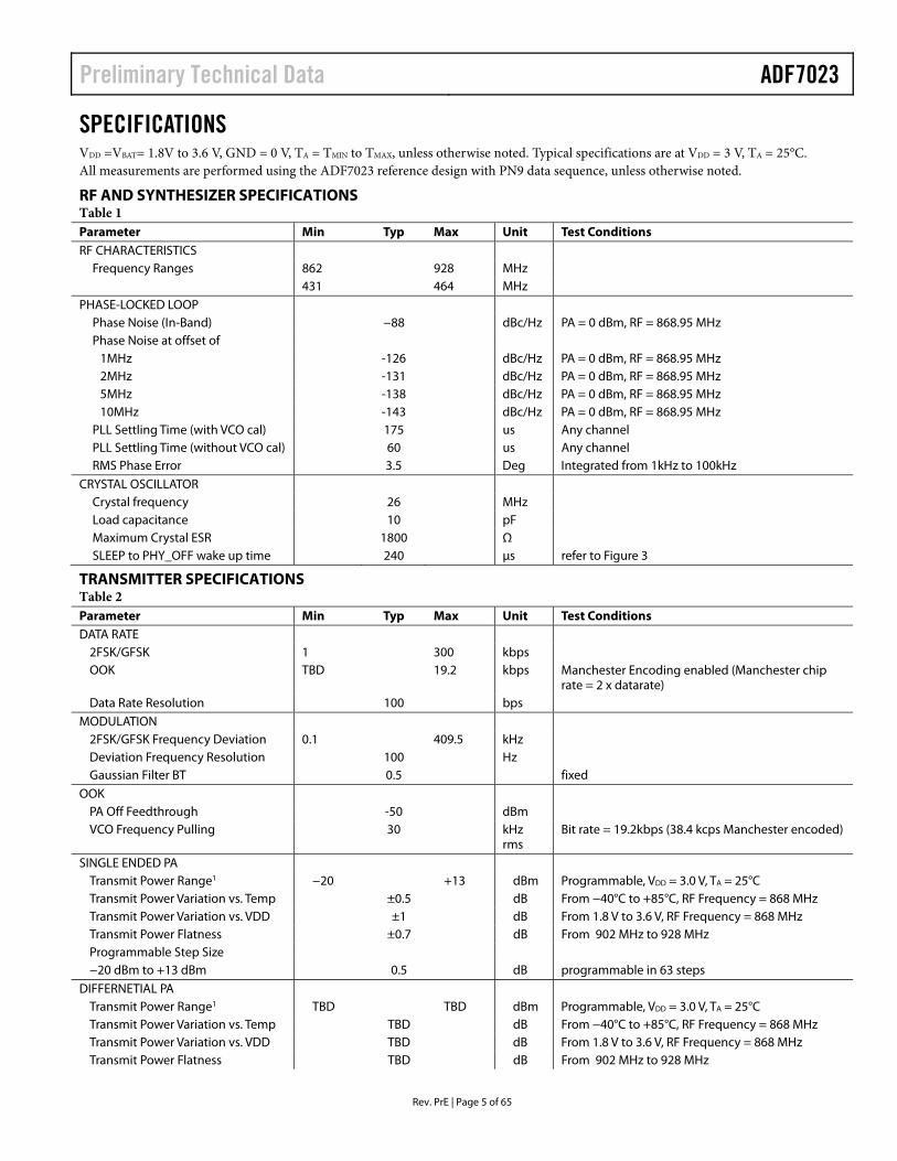
SPECIFICATIONS VDD =VBAT= 1.8V to 3.6 V, GND = 0 V, TA = TMIN to TMAX, unless otherwise noted. Typical specifications are at VDD = 3 V, TA = 25°C. All measurements are performed using the ADF7023 reference design with PN9 data sequence, unless otherwise noted.
RF AND SYNTHESIZER SPECIFICATIONS Table 1 Parameter Min Typ Max Unit Test Conditions RF CHARACTERISTICS
Frequency Ranges 862 928 MHz 431 464 MHz
PHASE-LOCKED LOOP Phase Noise (In-Band) −88 dBc/Hz PA = 0 dBm, RF = 868.95 MHz Phase Noise at offset of
1MHz -126 dBc/Hz PA = 0 dBm, RF = 868.95 MHz 2MHz -131 dBc/Hz PA = 0 dBm, RF = 868.95 MHz 5MHz -138 dBc/Hz PA = 0 dBm, RF = 868.95 MHz 10MHz -143 dBc/Hz PA = 0 dBm, RF = 868.95 MHz
PLL Settling Time (with VCO cal) 175 us Any channel PLL Settling Time (without VCO cal) 60 us Any channel RMS Phase Error 3.5 Deg Integrated from 1kHz to 100kHz
CRYSTAL OSCILLATOR Crystal frequency 26 MHz Load capacitance 10 pF Maximum Crystal ESR 1800 Ω SLEEP to PHY_OFF wake up time 240 μs refer to Figure 3
TRANSMITTER SPECIFICATIONS Table 2 Parameter Min Typ Max Unit Test Conditions DATA RATE
2FSK/GFSK 1 300 kbps OOK TBD 19.2 kbps Manchester Encoding enabled (Manchester chip
rate = 2 x datarate) Data Rate Resolution 100 bps
MODULATION 2FSK/GFSK Frequency Deviation 0.1 409.5 kHz Deviation Frequency Resolution 100 Hz Gaussian Filter BT 0.5 fixed
OOK PA Off Feedthrough -50 dBm VCO Frequency Pulling 30 kHz
rms Bit rate = 19.2kbps (38.4 kcps Manchester encoded)
SINGLE ENDED PA Transmit Power Range1 −20 +13 dBm Programmable, VDD = 3.0 V, TA = 25°C Transmit Power Variation vs. Temp ±0.5 dB From −40°C to +85°C, RF Frequency = 868 MHz Transmit Power Variation vs. VDD ±1 dB From 1.8 V to 3.6 V, RF Frequency = 868 MHz Transmit Power Flatness ±0.7 dB From 902 MHz to 928 MHz Programmable Step Size −20 dBm to +13 dBm 0.5 dB programmable in 63 steps
DIFFERNETIAL PA Transmit Power Range1 TBD TBD dBm Programmable, VDD = 3.0 V, TA = 25°C Transmit Power Variation vs. Temp TBD dB From −40°C to +85°C, RF Frequency = 868 MHz Transmit Power Variation vs. VDD TBD dB From 1.8 V to 3.6 V, RF Frequency = 868 MHz Transmit Power Flatness TBD dB From 902 MHz to 928 MHz
ADF7023 Preliminary Technical Data
Rev. PrE | Page 6 of 65
Programmable Step Size −20 dBm to +13 dBm TBD dB programmable in 63 steps
SPURIOUS EMISSIONS Integer Boundary Spurious TBD dBc receiver PLL closed loop bandwidth (92kHz) Reference Spurious TBD dBc
HARMONICS Single Ended PA
Second Harmonic TBD dBc Unfiltered conductive Third Harmonic TBD dBc Unfiltered conductive All Other Harmonics TBD dBc Unfiltered conductive
Differential PA Second Harmonic TBD dBc Unfiltered conductive Third Harmonic TBD dBc Unfiltered conductive All Other Harmonics TBD dBc Unfiltered conductive
OPTIMUM PA LOAD IMPEDANCE Single Ended PA
fRF = 915 MHz TBD Ω fRF = 868 MHz TBD Ω fRF = 433 MHz TBD Ω
Differential PA fRF = 915 MHz TBD Ω fRF = 868 MHz TBD Ω fRF = 433 MHz TBD Ω
1 Measured as maximum unmodulated power. Output power varies with both supply and temperature.
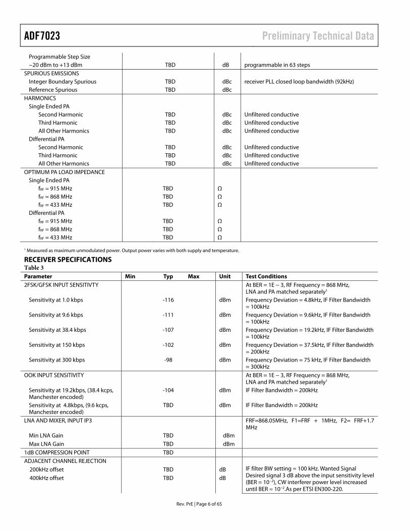
RECEIVER SPECIFICATIONS Table 3 Parameter Min Typ Max Unit Test Conditions 2FSK/GFSK INPUT SENSITIVTY At BER = 1E − 3, RF Frequency = 868 MHz,
LNA and PA matched separately1 Sensitivity at 1.0 kbps -116 dBm Frequency Deviation = 4.8kHz, IF Filter Bandwidth
= 100kHz Sensitivity at 9.6 kbps -111 dBm Frequency Deviation = 9.6kHz, IF Filter Bandwidth
= 100kHz Sensitivity at 38.4 kbps -107 dBm Frequency Deviation = 19.2kHz, IF Filter Bandwidth
= 100kHz Sensitivity at 150 kbps -102 dBm Frequency Deviation = 37.5kHz, IF Filter Bandwidth
= 200kHz Sensitivity at 300 kbps -98 dBm Frequency Deviation = 75 kHz, IF Filter Bandwidth
= 300kHz OOK INPUT SENSITIVITY At BER = 1E − 3, RF Frequency = 868 MHz,
LNA and PA matched separately1
Sensitivity at 19.2kbps, (38.4 kcps, Manchester encoded)
-104 dBm IF Filter Bandwidth = 200kHz
Sensitivity at 4.8kbps, (9.6 kcps, Manchester encoded)
TBD dBm IF Filter Bandwidth = 200kHz
LNA AND MIXER, INPUT IP3 FRF=868.05MHz, F1=FRF + 1MHz, F2= FRF+1.7 MHz
Min LNA Gain TBD dBm Max LNA Gain TBD dBm
1dB COMPRESSION POINT TBD ADJACENT CHANNEL REJECTION
IF filter BW setting = 100 kHz. Wanted Signal Desired signal 3 dB above the input sensitivity level (BER = 10−2), CW interferer power level increased until BER = 10−2.As per ETSI EN300-220.
200kHz offset TBD dB 400kHz offset TBD dB
Preliminary Technical Data ADF7023
Rev. PrE | Page 7 of 65
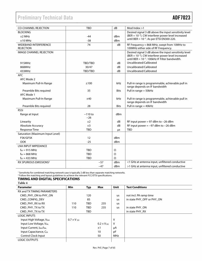
CO-CHANNEL REJECTION TBD dB Mod Index >1 BLOCKING Desired signal 3 dB above the input sensitivity level
(BER = 10−2). CW interferer power level increased until BER = 10−2. As per ETSI EN300-220.
±2 MHz -44 dBm ±10 MHz -38 dBm
WIDEBAND INTERFERENCE REJECTION
74 dB RF Frequency = 868 MHz, swept from 10MHz to 100MHz either side of RF Frequency.
IMAGE CHANNEL REJECTION Desired signal 3 dB above the input sensitivity level (BER = 10−2). CW interferer power level increased until BER = 10−2. 100kHz IF Filter bandwidth.
915MHz TBD/TBD dB Uncalibrated/Calibrated
868MHz 30/47 dB Uncalibrated/Calibrated 433MHz TBD/TBD dB Uncalibrated/Calibrated
AFC AFC Mode 2
Maximum Pull-In Range ±100 kHz Pull-in range is programmable, achievable pull in range depends on IF bandwidth
Preamble Bits required 35 Bits Pull in range = 50kHz AFC Mode 1
Maximum Pull-In Range ±40 kHz Pull-in range is programmable, achievable pull in range depends on IF bandwidth
Preamble Bits required 28 Bits Pull in range = 40kHz RSSI
Range at Input −110 to −26
dBm
Linearity ±2 dB RF input power = 97 dBm to −26 dBm Absolute Accuracy ±3 dB RF input power = −97 dBm to −26 dBm Response Time TBD μs TBD
Saturation (Maximum Input Level) FSK/GFSK 12 dBm OOK -25 dBm
LNA INPUT IMPEDANCE fRF = 915 MHz TBD Ω fRF = 868 MHz TBD Ω fRF = 433 MHz TBD Ω
RX SPURIOUS EMISSIONS2 −57 dBm <1 GHz at antenna input, unfiltered conductive
−47 dBm >1 GHz at antenna input, unfiltered conductive 1 Sensitivity for combined matching network case is typically 2 dB less than separate matching networks. 2 Follow the matching and layout guidelines to achieve the relevant FCC/ETSI specifications.
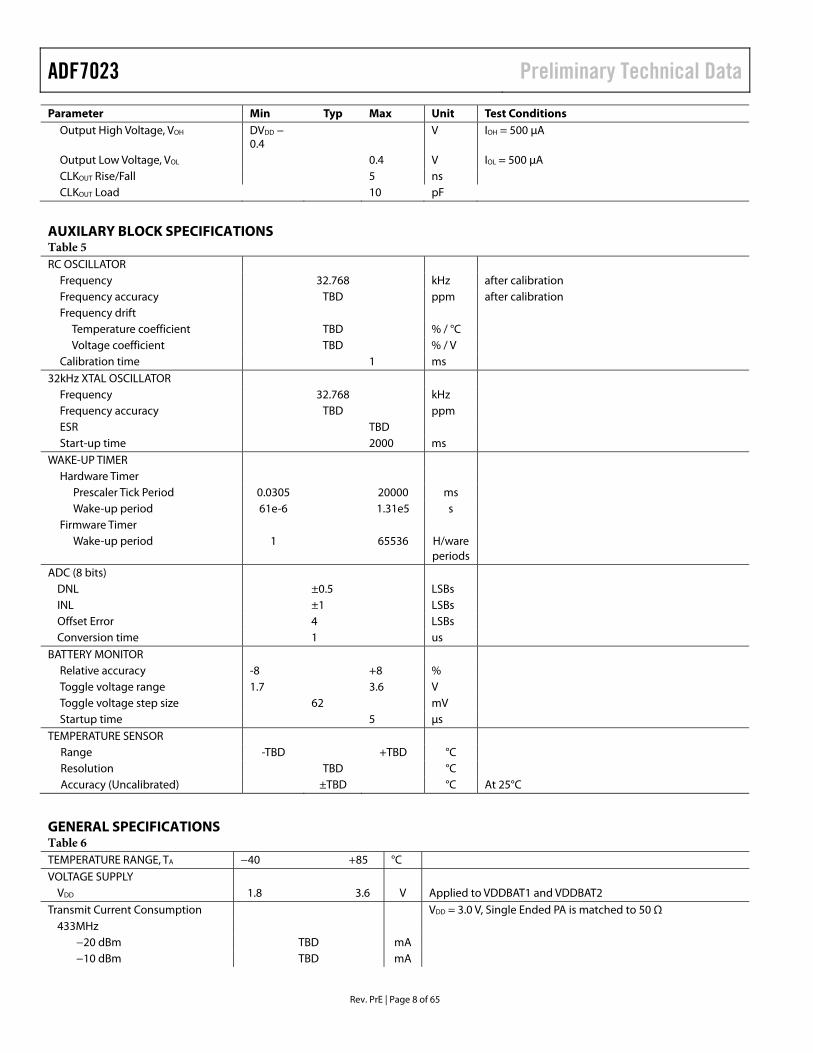
TIMING AND DIGITAL SPECIFICATIONS Table 4 Parameter Min Typ Max Unit Test Conditions RX and TX TIMING PARAMETERS
CMD_PHY_ON to PHY_ON 120 us not incl. PA ramp time CMD_CONFIG_DEV 85 us in state PHY_OFF or PHY_ON CMD_PHY_RX to RX 110 TBD 235 us CMD_PHY_TX to TX 110 TBD 235 us in state PHY_ON CMD_PHY_TX to TX TBD in state PHY_RX
LOGIC INPUTS Input High Voltage, VINH 0.7 × V DD V Input Low Voltage, VINL 0.2 × V DD V Input Current, IINH/IINL ±1 μA Input Capacitance, CIN 10 pF Control Clock Input 50 MHz
LOGIC OUTPUTS
ADF7023 Preliminary Technical Data
Rev. PrE | Page 8 of 65
Parameter Min Typ Max Unit Test Conditions Output High Voltage, VOH DVDD −
0.4 V IOH = 500 μA
Output Low Voltage, VOL 0.4 V IOL = 500 μA CLKOUT Rise/Fall 5 ns CLKOUT Load 10 pF
AUXILARY BLOCK SPECIFICATIONS Table 5 RC OSCILLATOR
Frequency 32.768 kHz after calibration Frequency accuracy TBD ppm after calibration Frequency drift
Temperature coefficient TBD % / °C Voltage coefficient TBD % / V
Calibration time 1 ms 32kHz XTAL OSCILLATOR
Frequency 32.768 kHz Frequency accuracy TBD ppm ESR TBD Start-up time 2000 ms
WAKE-UP TIMER Hardware Timer
Prescaler Tick Period 0.0305 20000 ms Wake-up period 61e-6 1.31e5 s
Firmware Timer Wake-up period 1 65536 H/ware
periods
ADC (8 bits) DNL ±0.5 LSBs INL ±1 LSBs Offset Error 4 LSBs Conversion time 1 us
BATTERY MONITOR Relative accuracy -8 +8 %
Toggle voltage range 1.7 3.6 V Toggle voltage step size 62 mV Startup time 5 μs
TEMPERATURE SENSOR Range -TBD +TBD °C Resolution TBD °C Accuracy (Uncalibrated) ±TBD °C At 25°C
GENERAL SPECIFICATIONS Table 6 TEMPERATURE RANGE, TA −40 +85 °C VOLTAGE SUPPLY
VDD 1.8 3.6 V Applied to VDDBAT1 and VDDBAT2 Transmit Current Consumption VDD = 3.0 V, Single Ended PA is matched to 50 Ω
433MHz −20 dBm TBD mA −10 dBm TBD mA
Preliminary Technical Data ADF7023
Rev. PrE | Page 9 of 65
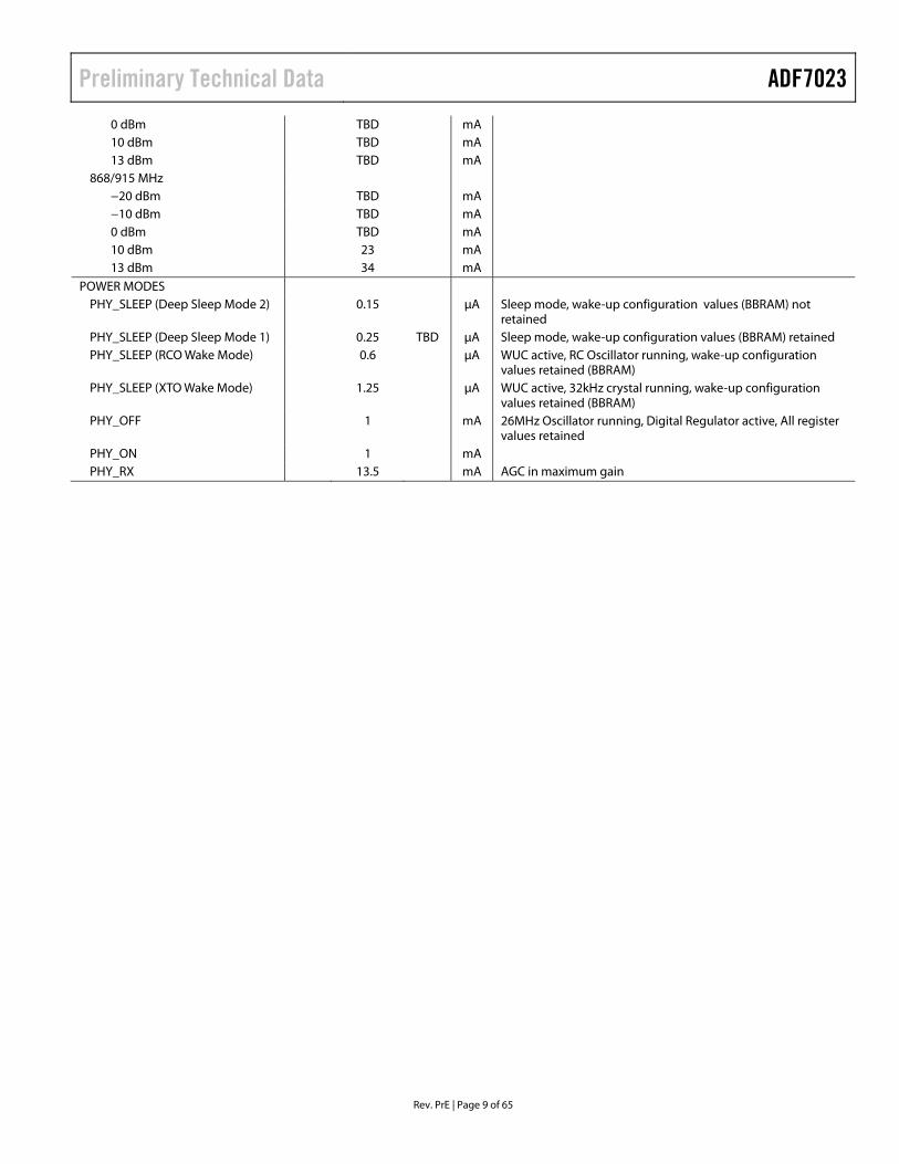
0 dBm TBD mA 10 dBm TBD mA 13 dBm TBD mA
868/915 MHz −20 dBm TBD mA −10 dBm TBD mA 0 dBm TBD mA 10 dBm 23 mA 13 dBm 34 mA
POWER MODES PHY_SLEEP (Deep Sleep Mode 2) 0.15 μA Sleep mode, wake-up configuration values (BBRAM) not
retained PHY_SLEEP (Deep Sleep Mode 1) 0.25 TBD μA Sleep mode, wake-up configuration values (BBRAM) retained PHY_SLEEP (RCO Wake Mode) 0.6 μA WUC active, RC Oscillator running, wake-up configuration
values retained (BBRAM) PHY_SLEEP (XTO Wake Mode) 1.25 μA WUC active, 32kHz crystal running, wake-up configuration
values retained (BBRAM) PHY_OFF 1 mA 26MHz Oscillator running, Digital Regulator active, All register
values retained PHY_ON 1 mA PHY_RX 13.5 mA AGC in maximum gain
ADF7023 Preliminary Technical Data
Rev. PrE | Page 10 of 65
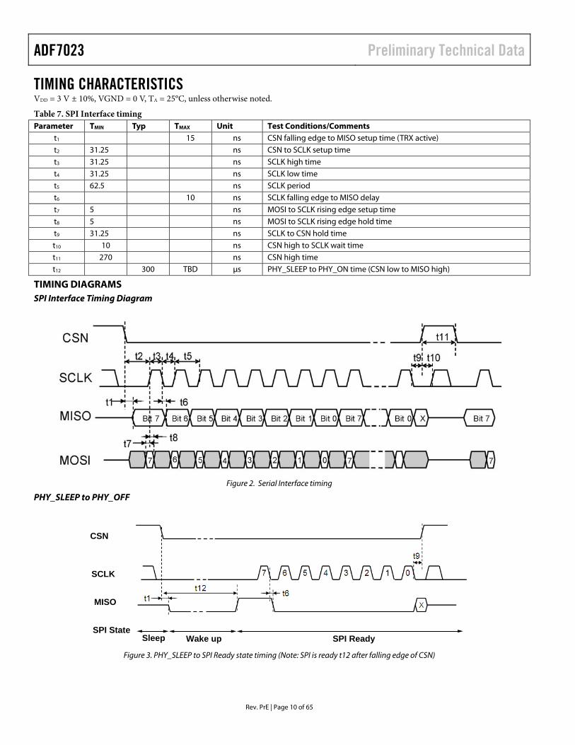
TIMING CHARACTERISTICS VDD = 3 V ± 10%, VGND = 0 V, TA = 25°C, unless otherwise noted.
Table 7. SPI Interface timing Parameter TMIN Typ TMAX Unit Test Conditions/Comments
t1 15 ns CSN falling edge to MISO setup time (TRX active) t2 31.25 ns CSN to SCLK setup time t3 31.25 ns SCLK high time t4 31.25 ns SCLK low time t5 62.5 ns SCLK period t6 10 ns SCLK falling edge to MISO delay t7 5 ns MOSI to SCLK rising edge setup time t8 5 ns MOSI to SCLK rising edge hold time t9 31.25 ns SCLK to CSN hold time t10 10 ns CSN high to SCLK wait time t11 270 ns CSN high time t12 300 TBD μs PHY_SLEEP to PHY_ON time (CSN low to MISO high)
TIMING DIAGRAMS SPI Interface Timing Diagram
Figure 2. Serial Interface timing
PHY_SLEEP to PHY_OFF
Figure 3. PHY_SLEEP to SPI Ready state timing (Note: SPI is ready t12 after falling edge of CSN)
SPI State
CSN
SCLK
MISO
Sleep Wake up SPI Ready
Preliminary Technical Data ADF7023
Rev. PrE | Page 11 of 65
ABSOLUTE MAXIMUM RATINGS TA = 25°C, unless otherwise noted.
Table 8 Parameter Rating VDD to GND1 −0.3 V to +3.6 V Operating Temperature Range
Industrial −40°C to +85°C Storage Temperature Range −65°C to +125°C Maximum Junction Temperature 150°C MLF θJA Thermal Impedance 26°C/W Reflow Soldering
Peak Temperature 260°C Time at Peak Temperature 40 sec
1 GND = RFGND = VCO GND = 0 V.
The exposed paddle of the LFCSP package should be connected to ground.
Stresses above those listed under Absolute Maximum Ratings may cause permanent damage to the device. This is a stress rating only and functional operation of the device at these or any other conditions above those indicated in the operational section of this specification is not implied. Exposure to absolute maximum rating conditions for extended periods may affect device reliability.
This device is a high performance RF integrated circuit with an ESD rating of <2 kV, and it is ESD sensitive. Proper precautions should be taken for handling and assembly.
ESD CAUTION ESD (electrostatic discharge) sensitive device. Electrostatic charges as high as 4000 V readily accumulate on the human body and test equipment and can discharge without detection. Although this product features proprietary ESD protection circuitry, permanent damage may occur on devices subjected to high energy electrostatic discharges. Therefore, proper ESD precautions are recommended to avoid performance degradation or loss of functionality.
ADF7023 Preliminary Technical Data
Rev. PrE | Page 12 of 65
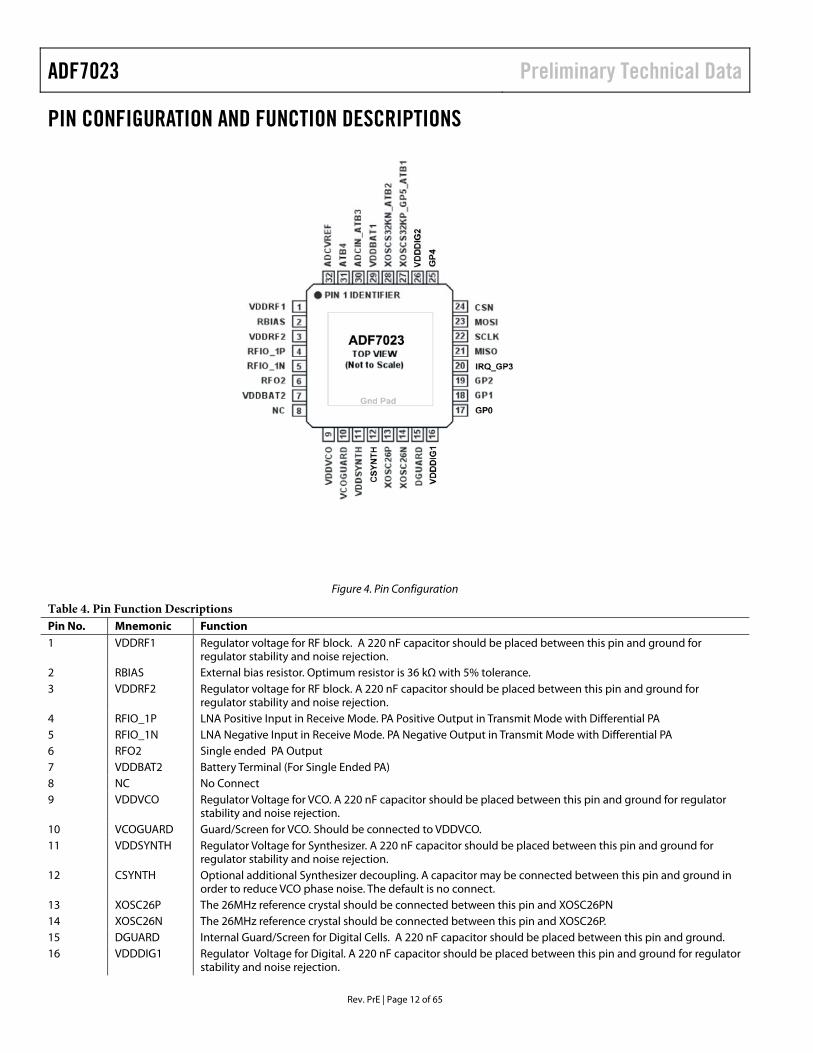
PIN CONFIGURATION AND FUNCTION DESCRIPTIONS
Figure 4. Pin Configuration
Table 4. Pin Function Descriptions Pin No. Mnemonic Function 1 VDDRF1 Regulator voltage for RF block. A 220 nF capacitor should be placed between this pin and ground for
regulator stability and noise rejection. 2 RBIAS External bias resistor. Optimum resistor is 36 kΩ with 5% tolerance. 3 VDDRF2 Regulator voltage for RF block. A 220 nF capacitor should be placed between this pin and ground for
regulator stability and noise rejection. 4 RFIO_1P LNA Positive Input in Receive Mode. PA Positive Output in Transmit Mode with Differential PA 5 RFIO_1N LNA Negative Input in Receive Mode. PA Negative Output in Transmit Mode with Differential PA 6 RFO2 Single ended PA Output 7 VDDBAT2 Battery Terminal (For Single Ended PA) 8 NC No Connect 9 VDDVCO Regulator Voltage for VCO. A 220 nF capacitor should be placed between this pin and ground for regulator
stability and noise rejection. 10 VCOGUARD Guard/Screen for VCO. Should be connected to VDDVCO. 11 VDDSYNTH Regulator Voltage for Synthesizer. A 220 nF capacitor should be placed between this pin and ground for
regulator stability and noise rejection. 12 CSYNTH Optional additional Synthesizer decoupling. A capacitor may be connected between this pin and ground in
order to reduce VCO phase noise. The default is no connect. 13 XOSC26P The 26MHz reference crystal should be connected between this pin and XOSC26PN 14 XOSC26N The 26MHz reference crystal should be connected between this pin and XOSC26P. 15 DGUARD Internal Guard/Screen for Digital Cells. A 220 nF capacitor should be placed between this pin and ground. 16 VDDDIG1 Regulator Voltage for Digital. A 220 nF capacitor should be placed between this pin and ground for regulator
stability and noise rejection.
Preliminary Technical Data ADF7023
Rev. PrE | Page 13 of 65
Pin No. Mnemonic Function 17 GP0 Digital GPIO Test Pin 0 18 GP1 Digital GPIO Test Pin 1 19 GP2 Digital GPIO Test Pin 2 20 IRQ_GP3 Interrupt Request, Digital GPIO Test Pin 3 21 MISO Serial Port Master In Slave Out 22 SCLK Serial Port Clock 23 MOSI Serial Port Master Out Slave In 24 CSN Chip Enable (Active Low) 25 GP4 Digital GPIO Test Pin 4 26 VDDDIG2 Regulator Voltage for Digital. A 220 nF capacitor should be placed between this pin and ground for regulator
stability and noise rejection. 27 XOSC32KP_
GP5_ATB1 The 32kHz watch xtal should be connected between this pin and XOSC32KN Analog Test Bus 1
28 XOSC32KN_ ATB2
The 32kHz watch xtal should be connected between this pin and XOSC32KP. Analog test bus 2
29 VDDBAT1 Battery Terminal 30 ADCIN_ATB3 Analog-to-Digital Converter Input.
Analog test bus 3
ADF7023 Preliminary Technical Data
Rev. PrE | Page 14 of 65
TYPICAL PERFORMANCE CHARACTERISTICS
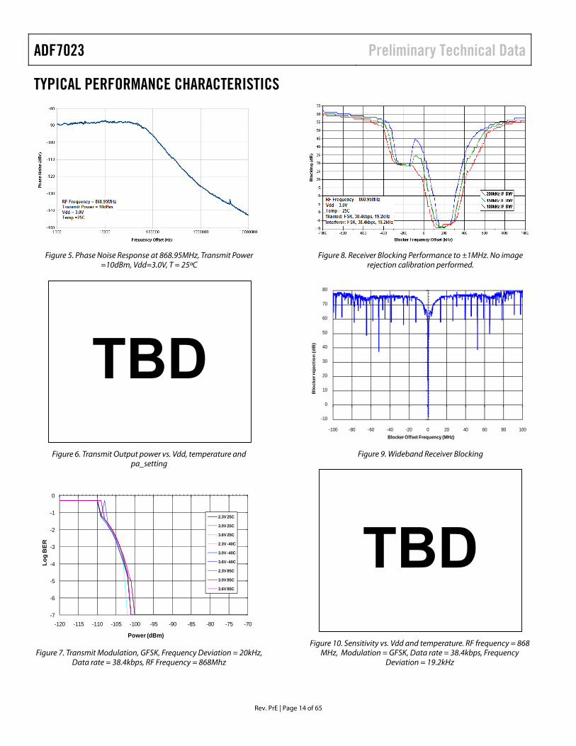
Figure 5. Phase Noise Response at 868.95MHz, Transmit Power =10dBm, Vdd=3.0V, T = 25ºC
Figure 6. Transmit Output power vs. Vdd, temperature and pa_setting
Figure 7. Transmit Modulation, GFSK, Frequency Deviation = 20kHz, Data rate = 38.4kbps, RF Frequency = 868Mhz
Figure 8. Receiver Blocking Performance to ±1MHz. No image rejection calibration performed.
Figure 9. Wideband Receiver Blocking
Figure 10. Sensitivity vs. Vdd and temperature. RF frequency = 868 MHz, Modulation = GFSK, Data rate = 38.4kbps, Frequency
Deviation = 19.2kHz
-7
-6
-5
-4
-3
-2
-1
0
-120 -115 -110 -105 -100 -95 -90 -85 -80 -75 -70
Log
BE
R
Power (dBm)
2.3V 25C
3.0V 25C
3.6V 25C
2.3V -40C
3.0V -40C
3.6V -40C
2.3V 85C
3.0V 85C
3.6V 85C
-10
0
10
20
30
40
50
60
70
80
-100 -80 -60 -40 -20 0 20 40 60 80 100
Blo
cker
reje
ctio
n (d
B)
Blocker Offset Frequency (MHz)
Preliminary Technical Data ADF7023
Rev. PrE | Page 15 of 65
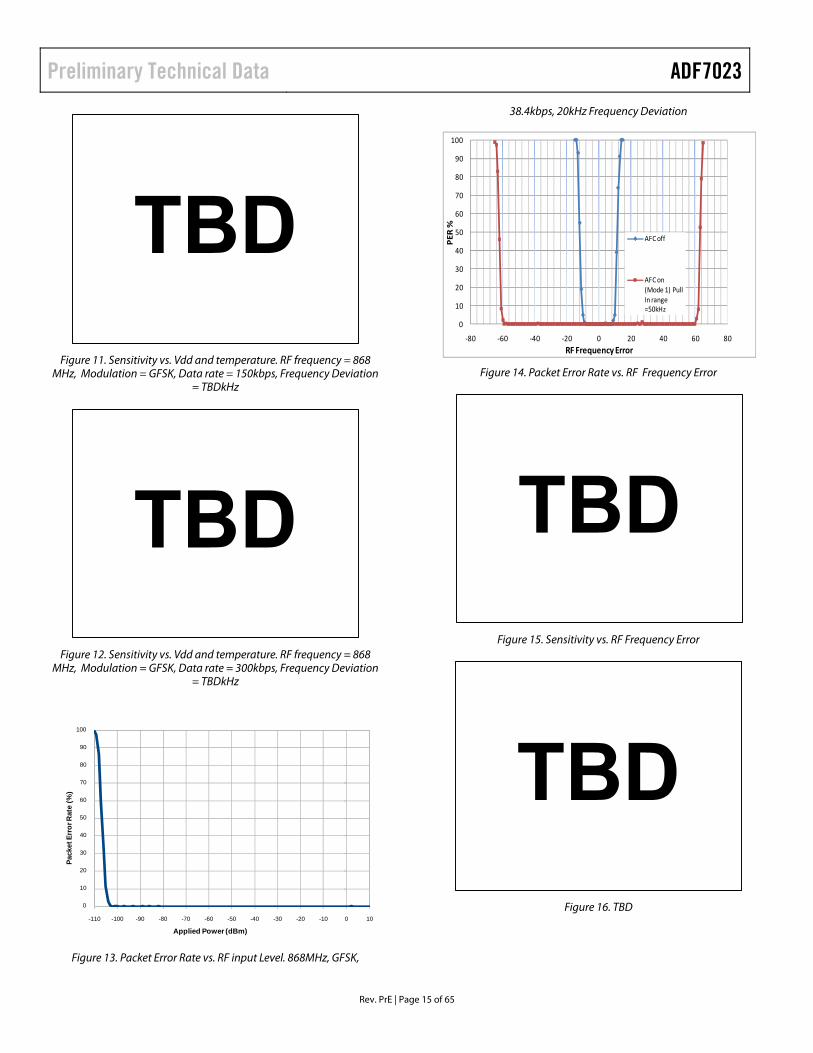
Figure 11. Sensitivity vs. Vdd and temperature. RF frequency = 868 MHz, Modulation = GFSK, Data rate = 150kbps, Frequency Deviation
= TBDkHz
Figure 12. Sensitivity vs. Vdd and temperature. RF frequency = 868 MHz, Modulation = GFSK, Data rate = 300kbps, Frequency Deviation
= TBDkHz
Figure 13. Packet Error Rate vs. RF input Level. 868MHz, GFSK,
38.4kbps, 20kHz Frequency Deviation
Figure 14. Packet Error Rate vs. RF Frequency Error
Figure 15. Sensitivity vs. RF Frequency Error
Figure 16. TBD
0
10
20
30
40
50
60
70
80
90
100
-110 -100 -90 -80 -70 -60 -50 -40 -30 -20 -10 0 10
Pack
et E
rror
Rat
e (%
)
Applied Power (dBm)
0
10
20
30
40
50
60
70
80
90
100
‐80 ‐60 ‐40 ‐20 0 20 40 60 80
PER
%
RF Frequency Error
AFC off
AFC on (Mode 1) Pull In range =50kHz
ADF7023 Preliminary Technical Data
Rev. PrE | Page 16 of 65
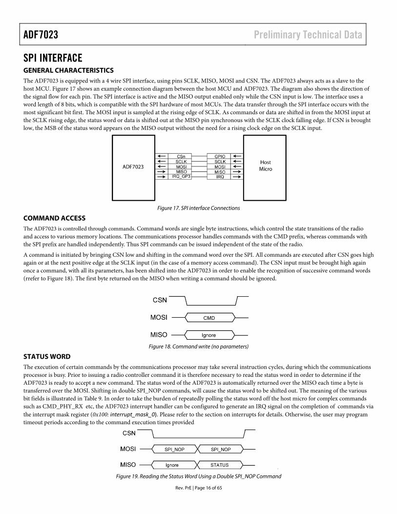
SPI INTERFACE GENERAL CHARACTERISTICS The ADF7023 is equipped with a 4 wire SPI interface, using pins SCLK, MISO, MOSI and CSN. The ADF7023 always acts as a slave to the host MCU. Figure 17 shows an example connection diagram between the host MCU and ADF7023. The diagram also shows the direction of the signal flow for each pin. The SPI interface is active and the MISO output enabled only while the CSN input is low. The interface uses a word length of 8 bits, which is compatible with the SPI hardware of most MCUs. The data transfer through the SPI interface occurs with the most significant bit first. The MOSI input is sampled at the rising edge of SCLK. As commands or data are shifted in from the MOSI input at the SCLK rising edge, the status word or data is shifted out at the MISO pin synchronous with the SCLK clock falling edge. If CSN is brought low, the MSB of the status word appears on the MISO output without the need for a rising clock edge on the SCLK input.
Figure 17. SPI interface Connections
COMMAND ACCESS The ADF7023 is controlled through commands. Command words are single byte instructions, which control the state transitions of the radio and access to various memory locations. The communications processor handles commands with the CMD prefix, whereas commands with the SPI prefix are handled independently. Thus SPI commands can be issued independent of the state of the radio.
A command is initiated by bringing CSN low and shifting in the command word over the SPI. All commands are executed after CSN goes high again or at the next positive edge at the SCLK input (in the case of a memory access command). The CSN input must be brought high again once a command, with all its parameters, has been shifted into the ADF7023 in order to enable the recognition of successive command words (rrefer to Figure 18). The first byte returned on the MISO when writing a command should be ignored.
Figure 18. Command write (no parameters)
STATUS WORD The execution of certain commands by the communications processor may take several instruction cycles, during which the communications processor is busy. Prior to issuing a radio controller command it is therefore necessary to read the status word in order to determine if the ADF7023 is ready to accept a new command. The status word of the ADF7023 is automatically returned over the MISO each time a byte is transferred over the MOSI. Shifting in double SPI_NOP commands, will cause the status word to be shifted out. The meaning of the various bit fields is illustrated in Table 9. In order to take the burden of repeatedly polling the status word off the host micro for complex commands such as CMD_PHY_RX etc, the ADF7023 interrupt handler can be configured to generate an IRQ signal on the completion of commands via the interrupt mask register (0x100: interrupt_mask_0). Please refer to the section on interrupts for details. Otherwise, the user may program timeout periods according to the command execution times provided
Figure 19. Reading the Status Word Using a Double SPI_NOP Command
Preliminary Technical Data ADF7023
Rev. PrE | Page 17 of 65
Table 9. Status Word
Bit Name Description
7 spi_ready 0: SPI is not ready for access, 1: SPI is ready for access
6 irq_status 0: No pending interrupt condition, 1: Pending interrupt condition (mirrors IRQ pin)
5 rc_ready 0: Radio Controller is not ready to receive a command, 1: Radio Controller is ready to receive a command
[4:0] reserved Reads 0
MEMORY WRITE/READ Memory locations are accessed by invoking the relevant SPI command. An 11 bit address is used to identify registers or locations in the memory space. The most significant 3 bits of the address are incorporated into the command by appending them as the lsbs of the command word. Figure 20 illustrates the command, address and data partitioning.
Figure 20.SPI Memory Access Command/Address Format
Block Write
MCR, BBRAM and Packet RAM memory locations can be written to in block format using the SPI_MEM_WR command. The SPI_MEM_WR command code is 00011xxxb, where xxxb represent Bits[10:8] of the first 11-bit address. If more than one data byte is written, the write address is automatically incremented for every byte sent until CSN =1 terminates the command. The maximum block write is 256 bytes. Refer to Figure 21 for more details.
Figure 21. Memory(MCR, BBRAM or Packet RAM) Block Write
Example
In this example it is desired to write to the adc_config_high register (0x35A: adc_config_high). Firstly, the CSN line should be set low to initiate SPI access.The 11-bit address of this register is 01101011010b (0x35Ah). Using the SPI_MEM_WR command and using the first most significant bits of the address the command word becomes 00011011b. The following byte consists of the remaining 8-bits of the register address, in this case 01011010b. So the command byte is 0x1Bh and the address byte is 0x5Ah. The data byte follows the address byte after which CSN=1 terminates the command.
Random Address Write
MCR, BBRAM and Packet RAM memory locations can be written to in random address format using the SPI_MEMR_WR command. The SPI_MEMR_WR command code is 00001xxxb, where xxxb represent bits[10:8] of the 11-bit address. The lower 8 bits of the address should
ADF7023 Preliminary Technical Data
Rev. PrE | Page 18 of 65
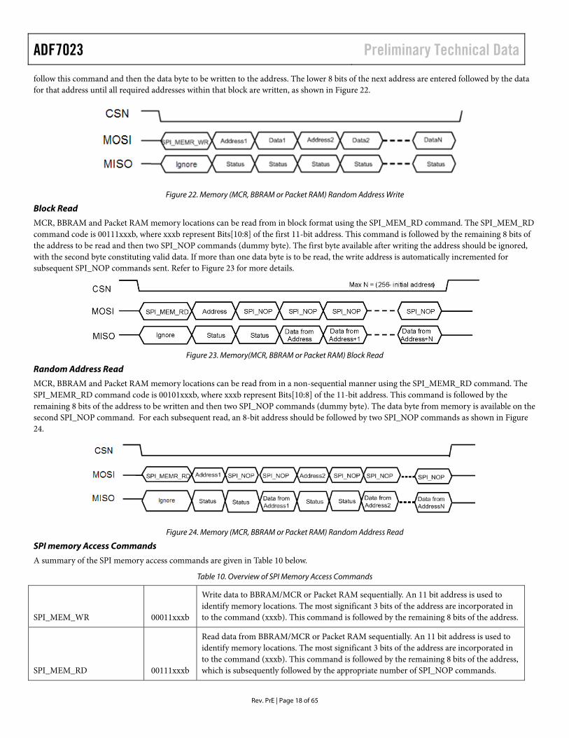
follow this command and then the data byte to be written to the address. The lower 8 bits of the next address are entered followed by the data for that address until all required addresses within that block are written, as shown in Figure 22.
Figure 22. Memory (MCR, BBRAM or Packet RAM) Random Address Write
Block Read
MCR, BBRAM and Packet RAM memory locations can be read from in block format using the SPI_MEM_RD command. The SPI_MEM_RD command code is 00111xxxb, where xxxb represent Bits[10:8] of the first 11-bit address. This command is followed by the remaining 8 bits of the address to be read and then two SPI_NOP commands (dummy byte). The first byte available after writing the address should be ignored, with the second byte constituting valid data. If more than one data byte is to be read, the write address is automatically incremented for subsequent SPI_NOP commands sent. Refer to Figure 23 for more details.
Figure 23. Memory(MCR, BBRAM or Packet RAM) Block Read
Random Address Read
MCR, BBRAM and Packet RAM memory locations can be read from in a non-sequential manner using the SPI_MEMR_RD command. The SPI_MEMR_RD command code is 00101xxxb, where xxxb represent Bits[10:8] of the 11-bit address. This command is followed by the remaining 8 bits of the address to be written and then two SPI_NOP commands (dummy byte). The data byte from memory is available on the second SPI_NOP command. For each subsequent read, an 8-bit address should be followed by two SPI_NOP commands as shown in Figure 24.
Figure 24. Memory (MCR, BBRAM or Packet RAM) Random Address Read
SPI memory Access Commands
A summary of the SPI memory access commands are given in Table 10 below.
Table 10. Overview of SPI Memory Access Commands
SPI_MEM_WR 00011xxxb
Write data to BBRAM/MCR or Packet RAM sequentially. An 11 bit address is used to identify memory locations. The most significant 3 bits of the address are incorporated in to the command (xxxb). This command is followed by the remaining 8 bits of the address.
SPI_MEM_RD 00111xxxb
Read data from BBRAM/MCR or Packet RAM sequentially. An 11 bit address is used to identify memory locations. The most significant 3 bits of the address are incorporated in to the command (xxxb). This command is followed by the remaining 8 bits of the address, which is subsequently followed by the appropriate number of SPI_NOP commands.
Preliminary Technical Data ADF7023
Rev. PrE | Page 19 of 65
SPI_MEMR_WR 00001xxxb Write data to BBRAM/MCR or Packet RAM at random.
SPI_MEMR_RD 00101xxxb Read data from BBRAM/MCR or Packet RAM at random.
SPI_NOP 0xFFFFh No operation. Use for dummy writes when polling the status_word. Used also as dummy data on the MOSI line when performing a memory read.
WAKE-UP FROM PHY_SLEEP STATE The host MCU can bring CSN low at any time in order to wake the ADF7023 from PHY_SLEEP state. After bringing CSN low, it must wait until the MISO output (spi_ready flag) goes high prior to accessing the SPI port. This delay reflects the start-up time of the ADF7023 (refer to Figure 3). Once the MISO output has gone high, the voltage regulator of the digital section and the 26MHz crystal oscillator have stabilized. Unless the chip was in PHY_SLEEP, the MISO pin will always go high immediately after taking CSN low, and further checking is no longer necessary.
PROGRAMMING SEQUENCE ON WAKE UP OR AFTER RESET On initial power of the communications processor or on wake up from PHY_SLEEP or after a communications processor reset it is necessary for the communications processor and host microcontroller to establish communication. This is accomplished by ensuring the host writes CMD_SYNC to the var_command location (memory location 0x000) and waits until the comms processor writes CMD_READY back to var_command.
If this procedure is not followed then it is possible that the first command written to the ADF7023 by the host may be over-written by the comms processor and not executed.
COMMS PROCESSOR RESET The CMD_RESET command can be issued at when the radio is any state. It re-initializes the comms processor and returns the radio to state PHY_OFF.
The BBRAM and MCR register settings are retained after reset while the packet RAM memory is re-initialized.
After a CMD_RESET the host should perform a re-synchronization with the comms processor using the CMD_SYNC procedure detailed in the Programming Sequence on Wake Up or After Reset section.
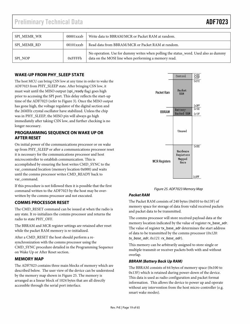
MEMORY MAP The ADF7023 contains three main blocks of memory which are described below. The user view of the device can be understood by the memory map shown in Figure 25. The memory is arranged as a linear block of 1024 bytes that are all directly accessible through the serial port interface.
Figure 25. ADF7023 Memory Map
Packet RAM
The Packet RAM consists of 240 bytes (0x010 to 0x13F) of memory space for storage of data from valid received packets and packet data to be transmitted.
The comms processor will store received payload data at the memory location indicated by the value of register rx_base_adr. The value of register tx_base_adr determines the start address of data to be transmitted by the comms processor (0x120: tx_base_adr, 0x121: rx_base_adr).
This memory can be arbitrarily assigned to store single or multiple transmit or receiver packets both with and without overlap.
BBRAM (Battery Back Up RAM)
The BBRAM consists of 64 bytes of memory space (0x100 to 0x13F) which is retained during power-down of the device. This data is used as radio configuration and packet format information. This allows the device to power up and operate without any intervention from the host micro-controller (e.g. smart wake modes).
ADF7023 Preliminary Technical Data
Rev. PrE | Page 20 of 65
If the BBRAM settings are changed then a CMD_CONIFG_DEV needs to be issued for the radio settings to be copied to the MCR.
MCR
The last 256 bytes of memory space (0x300 to 0x3FF) are mapped to the actual radio setup registers and can be used to directly set or observe the internal radio operation. When the packet handing capabilities of the communicatiosn preocessor are being used then only minimal interaction with this memory space is required (e.g. interrupt source, frequency error readback etc). Contents of MCR are lost during PHY_SLEEP state.
Reserved Packet RAM Locations
The first 16 bytes of packet RAM (0x000 to 0x00F) are reserved for use by the communications processor. However, some of these locations can be accessed by the user and are detailed in
Table 11.
Table 11. Useful memory locations in reserved packet RAM
Memory Location Name Function
0x00
Packet RAM
var_command Comms processor writes CMD_READY to this location when it’s ready to
accept commands. User writes CMD_SYNC to this location after power up, WUC wakeup or host microcontroller reset.
0x12
Packet RAM
var_state Current radio state. Can be read by the host at any time. No write access.
The state to readback value mapping is as follows:
0x0A: PHY_OFF
0x0B: PHY_ON
0x0C: PHY_RX
0x0D: PHY_TX
0x13
Packet RAM
var_tx_mode Transmit Test Modes. Used to set continuous carrier or modulation test modes. Read/write access by host.
Preliminary Technical Data ADF7023
Rev. PrE | Page 21 of 65
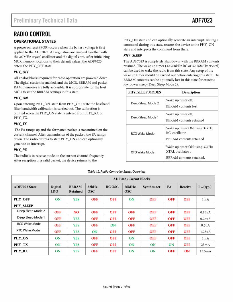
RADIO CONTROL OPERATIONAL STATES A power on reset (POR) occurs when the battery voltage is first applied to the ADF7023. All regulators are enabled together with the 26 MHz crystal oscillator and the digital core. After initializing MCR memory locations to their default values, the ADF7023 enters the PHY_OFF state.
PHY_OFF
All analog blocks required for radio operation are powered down. The digital section is enabled, and the MCR, BBRAM and packet RAM memories are fully accessible. It is appropriate for the host MCU to set the BBRAM settings in this state.
PHY_ON
Upon entering PHY_ON state from PHY_OFF state the baseband filter bandwidth calibration is carried out. The calibration is omitted when the PHY_ON state is entered from PHY_RX or PHY_TX.
PHY_TX
The PA ramps up and the formatted packet is transmitted on the current channel. After transmission of the packet, the PA ramps down. The radio returns to state PHY_ON and can optionally generate an interrupt.
PHY_RX
The radio is in receive mode on the current channel frequency. After reception of a valid packet, the device returns to the
PHY_ON state and can optionally generate an interrupt. Issuing a command during this state, returns the device to the PHY_ON state and interprets the command from there.
PHY_SLEEP
The ADF7023 is completely shut down with the BBRAM contents retained. The wake up timer (32.768kHz RC or 32.768kHz crystal) can be used to wake the radio from this state. Any setup of the wake up timer should be carried out before entering this state. The BBRAM contents can be optionally lost in this state for extreme low power sleep (Deep Sleep Mode 2).
PHY_SLEEP MODES Description
Deep Sleep Mode 2 Wake up timer off,
BBRAM contents lost
Deep Sleep Mode 1 Wake up timer off,
BBRAM contents retained
RCO Wake Mode
Wake up timer ON using 32kHz RC oscillator.
BBRAM contents retained
XTO Wake Mode
Wake up timer ON using 32kHz XTAL oscillator .
BBRAM contents retained.
Table 12. Radio Controller States Overview
ADF7023 Circuit Blocks
ADF7023 State Digital LDO
BBRAM Retained
32kHz OSC
RC OSC 26MHz OSC
Synthesizer PA Receive IDD (typ.)
PHY_OFF ON YES OFF OFF ON OFF OFF OFF 1mA
PHY_SLEEP Deep Sleep Mode 2 OFF NO OFF OFF OFF OFF OFF OFF 0.15uA Deep Sleep Mode 1 OFF YES OFF OFF OFF OFF OFF OFF 0.25uA RCO Wake Mode OFF YES OFF ON OFF OFF OFF OFF 0.6uA XTO Wake Mode OFF YES ON OFF OFF OFF OFF OFF 1.25uA
PHY_ON ON YES OFF OFF ON OFF OFF OFF 1mA
PHY_TX ON YES OFF OFF ON ON ON OFF 23mA
PHY_RX ON YES OFF OFF ON ON OFF ON 13.5mA
ADF7023 Preliminary Technical Data
Rev. PrE | Page 22 of 65
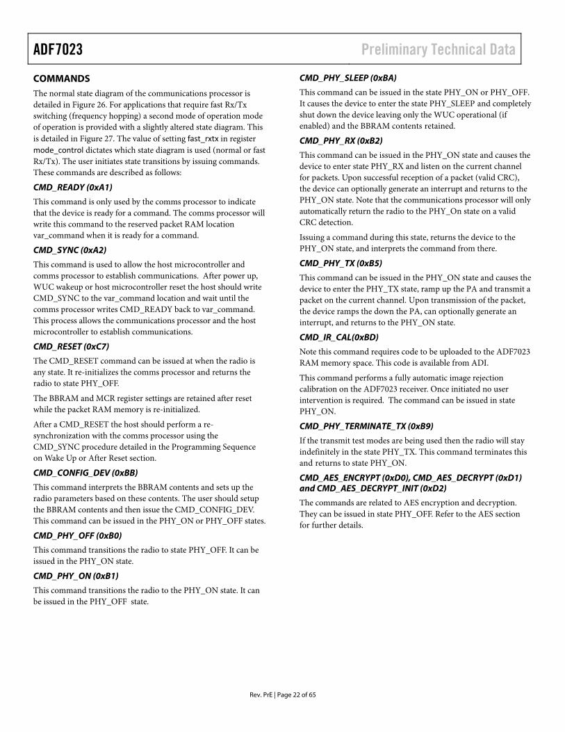
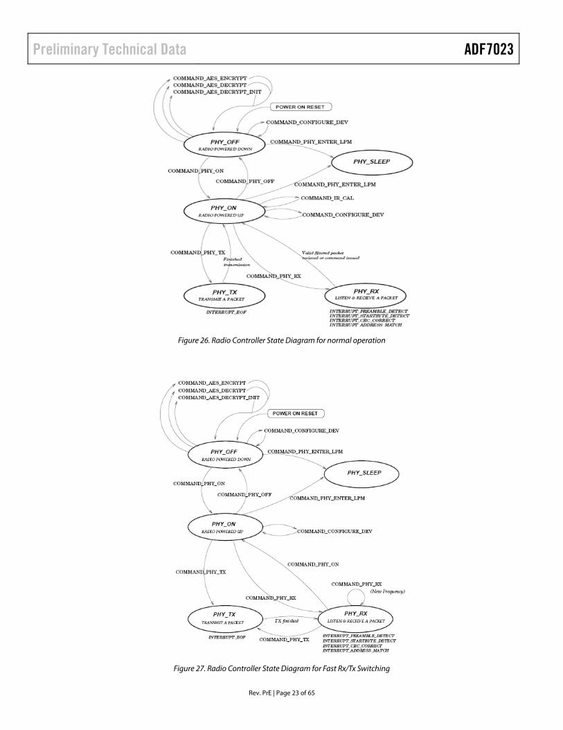
COMMANDS The normal state diagram of the communications processor is detailed in Figure 26. For applications that require fast Rx/Tx switching (frequency hopping) a second mode of operation mode of operation is provided with a slightly altered state diagram. This is detailed in Figure 27. The value of setting fast_rxtx in register mode_control dictates which state diagram is used (normal or fast Rx/Tx). The user initiates state transitions by issuing commands. These commands are described as follows:
CMD_READY (0xA1)
This command is only used by the comms processor to indicate that the device is ready for a command. The comms processor will write this command to the reserved packet RAM location var_command when it is ready for a command.
CMD_SYNC (0xA2)
This command is used to allow the host microcontroller and comms processor to establish communications. After power up, WUC wakeup or host microcontroller reset the host should write CMD_SYNC to the var_command location and wait until the comms processor writes CMD_READY back to var_command. This process allows the communications processor and the host microcontroller to establish communications.
CMD_RESET (0xC7)
The CMD_RESET command can be issued at when the radio is any state. It re-initializes the comms processor and returns the radio to state PHY_OFF.
The BBRAM and MCR register settings are retained after reset while the packet RAM memory is re-initialized.
After a CMD_RESET the host should perform a re-synchronization with the comms processor using the CMD_SYNC procedure detailed in the Programming Sequence on Wake Up or After Reset section.
CMD_CONFIG_DEV (0xBB)
This command interprets the BBRAM contents and sets up the radio parameters based on these contents. The user should setup the BBRAM contents and then issue the CMD_CONFIG_DEV. This command can be issued in the PHY_ON or PHY_OFF states.
CMD_PHY_OFF (0xB0)
This command transitions the radio to state PHY_OFF. It can be issued in the PHY_ON state.
CMD_PHY_ON (0xB1)
This command transitions the radio to the PHY_ON state. It can be issued in the PHY_OFF state.
CMD_PHY_SLEEP (0xBA)
This command can be issued in the state PHY_ON or PHY_OFF. It causes the device to enter the state PHY_SLEEP and completely shut down the device leaving only the WUC operational (if enabled) and the BBRAM contents retained.
CMD_PHY_RX (0xB2)
This command can be issued in the PHY_ON state and causes the device to enter state PHY_RX and listen on the current channel for packets. Upon successful reception of a packet (valid CRC), the device can optionally generate an interrupt and returns to the PHY_ON state. Note that the communications processor will only automatically return the radio to the PHY_On state on a valid CRC detection.
Issuing a command during this state, returns the device to the PHY_ON state, and interprets the command from there.
CMD_PHY_TX (0xB5)
This command can be issued in the PHY_ON state and causes the device to enter the PHY_TX state, ramp up the PA and transmit a packet on the current channel. Upon transmission of the packet, the device ramps the down the PA, can optionally generate an interrupt, and returns to the PHY_ON state.
CMD_IR_CAL(0xBD)
Note this command requires code to be uploaded to the ADF7023 RAM memory space. This code is available from ADI.
This command performs a fully automatic image rejection calibration on the ADF7023 receiver. Once initiated no user intervention is required. The command can be issued in state PHY_ON.
CMD_PHY_TERMINATE_TX (0xB9)
If the transmit test modes are being used then the radio will stay indefinitely in the state PHY_TX. This command terminates this and returns to state PHY_ON. CMD_AES_ENCRYPT (0xD0), CMD_AES_DECRYPT (0xD1) and CMD_AES_DECRYPT_INIT (0xD2)
The commands are related to AES encryption and decryption. They can be issued in state PHY_OFF. Refer to the AES section for further details.
Preliminary Technical Data ADF7023
Rev. PrE | Page 23 of 65
Figure 26. Radio Controller State Diagram for normal operation
Figure 27. Radio Controller State Diagram for Fast Rx/Tx Switching
ADF7023 Preliminary Technical Data
Rev. PrE | Page 24 of 65
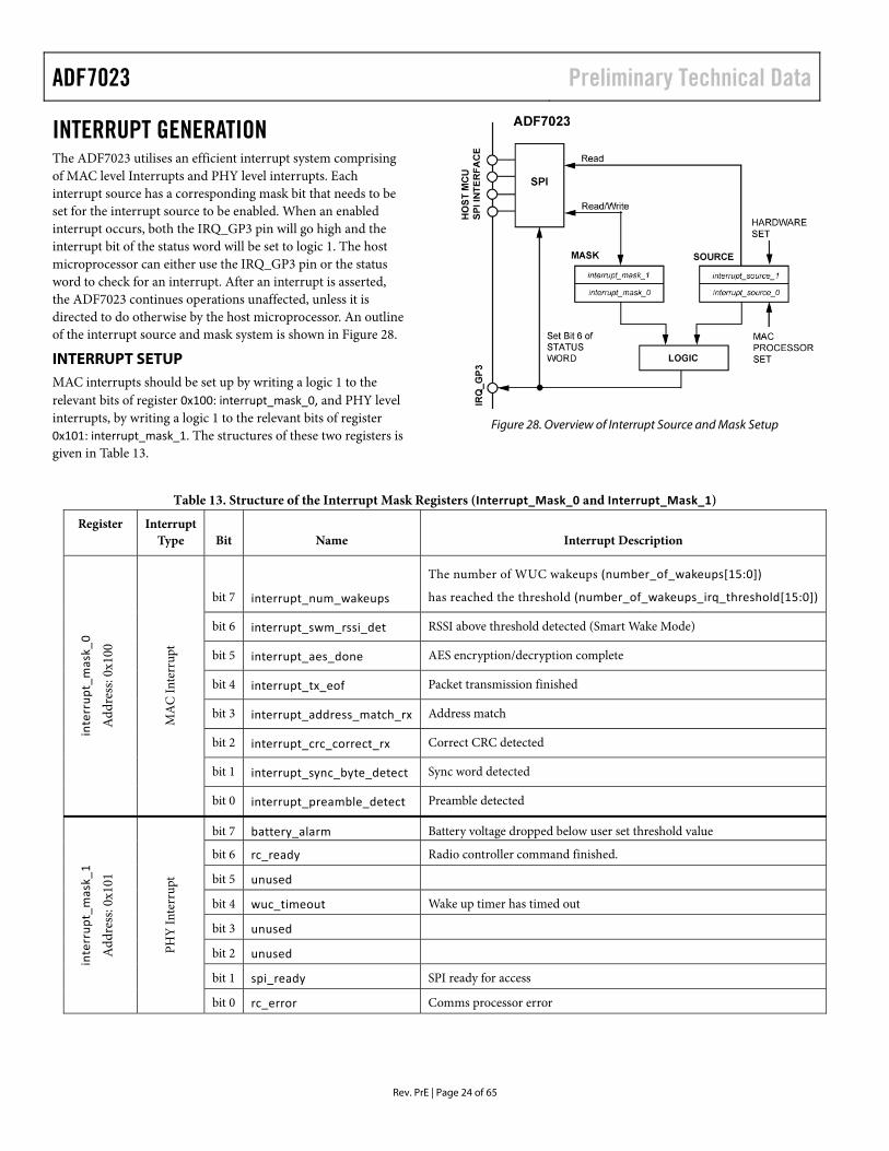
INTERRUPT GENERATION The ADF7023 utilises an efficient interrupt system comprising of MAC level Interrupts and PHY level interrupts. Each interrupt source has a corresponding mask bit that needs to be set for the interrupt source to be enabled. When an enabled interrupt occurs, both the IRQ_GP3 pin will go high and the interrupt bit of the status word will be set to logic 1. The host microprocessor can either use the IRQ_GP3 pin or the status word to check for an interrupt. After an interrupt is asserted, the ADF7023 continues operations unaffected, unless it is directed to do otherwise by the host microprocessor. An outline of the interrupt source and mask system is shown in Figure 28.
INTERRUPT SETUP MAC interrupts should be set up by writing a logic 1 to the relevant bits of register 0x100: interrupt_mask_0, and PHY level interrupts, by writing a logic 1 to the relevant bits of register 0x101: interrupt_mask_1. The structures of these two registers is given in Table 13.
Figure 28. Overview of Interrupt Source and Mask Setup
Table 13. Structure of the Interrupt Mask Registers (Interrupt_Mask_0 and Interrupt_Mask_1)
Register Interrupt Type Bit Name Interrupt Description
interrup
t_mask_0
Add
ress
: 0x1
00
MA
C In
terr
upt
bit 7 interrupt_num_wakeups
The number of WUC wakeups (number_of_wakeups[15:0])
has reached the threshold (number_of_wakeups_irq_threshold[15:0])
bit 6 interrupt_swm_rssi_det RSSI above threshold detected (Smart Wake Mode)
bit 5 interrupt_aes_done AES encryption/decryption complete
bit 4 interrupt_tx_eof Packet transmission finished
bit 3 interrupt_address_match_rx Address match
bit 2 interrupt_crc_correct_rx Correct CRC detected
bit 1 interrupt_sync_byte_detect Sync word detected
bit 0 interrupt_preamble_detect Preamble detected
interrup
t_mask_1
Add
ress
: 0x1
01
PHY
Inte
rrup
t
bit 7 battery_alarm Battery voltage dropped below user set threshold value
bit 6 rc_ready Radio controller command finished.
bit 5 unused
bit 4 wuc_timeout Wake up timer has timed out
bit 3 unused
bit 2 unused
bit 1 spi_ready SPI ready for access
bit 0 rc_error Comms processor error
Preliminary Technical Data ADF7023
Rev. PrE | Page 25 of 65
DETERMINING THE INTERRUPT SOURCE In the case of an interrupt condition, the interrupt source can be determined by reading the interrupt source registers (0x336: interrupt_source_0 and 0x337: interrupt_source_1). The bit that corresponds to the relevant interrupt condition will be high. The structure of these two registers is shown in Table 14.
Following an interrupt condition, the host microprocessor should clear the relevant interrupt flag, so that further interrupts will assert the IRQ_GP3 pin. This is performed by writing a logic 1 to the bit that is high in either the interrupt_source_0 or interrupt_source_1 registers. If multiple bits in the interrupt source registers are high, they can be cleared singly or altogether by writing logic 1s to them. The
IRQ_GP3 pin will go low when all the interrupt source bits are cleared.
As an example, take the case where a battery_alarm interrupt has occurred. The host microprocessor should:
1. Read the interrupt source registers. In this example if none of the interrupt flags in interrupt_source_0 were enabled, only interrupt_source_1 needs to be read.
2. Clear the interrupt by writing 0x80h (or 0xFFh) to the interrupt_source_1, 0x337 register.
3. Respond to the interrupt condition
Table 14. Structure of Interrupt Source Registers
Register Bit Name Interrupt Description
inte
rrup
t_so
urce
_0
Add
ress
: 0x3
36
bit 7 interrupt_num_wakeups Number of wakeups has reached threshold.
bit 6 interrupt_swm_rssi_det RSSI above threshold detected (Smart Wake Mode) interrupt
bit 5 interrupt_aes_done AES encryption/decryption complete
bit 4 interrupt_tx_eof Packet transmission finished interrupt
bit 3 interrupt_address_match_rx Address match interrupt
bit 2 interrupt_crc_correct_rx Correct CRC detect interrupt
bit 1 interrupt_sync_byte_detect Sync word detect interrupt
bit 0 interrupt_preamble_detect Preamble detect interrupt
inte
rrup
t_so
urce
_1
Add
ress
: 0x3
37
bit 7 battery_alarm Battery Voltage dropped below user set threshold value
bit 6 rc_ready Radio controller command finished interrupt. Ready to accept a new MAC command
bit 5 unused
bit 4 wuc_timeout Wake Up Counter has timed out interrupt
bit 3 unused
bit 2 unused
bit 1 spi_ready SPI ready for access
bit 0 rc_error Radio Controller error interrupt
ADF7023 Preliminary Technical Data
Rev. PrE | Page 26 of 65
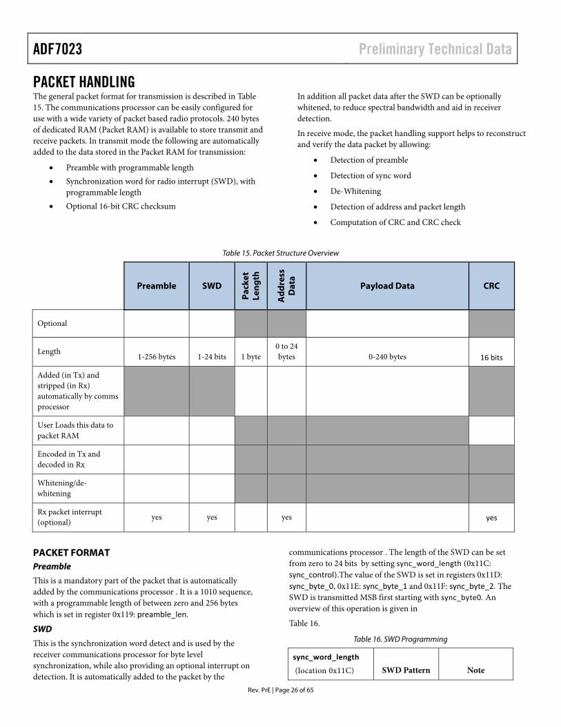
PACKET HANDLING The general packet format for transmission is described in Table 15. The communications processor can be easily configured for use with a wide variety of packet based radio protocols. 240 bytes of dedicated RAM (Packet RAM) is available to store transmit and receive packets. In transmit mode the following are automatically added to the data stored in the Packet RAM for transmission:
• Preamble with programmable length • Synchronization word for radio interrupt (SWD), with
programmable length • Optional 16-bit CRC checksum
In addition all packet data after the SWD can be optionally whitened, to reduce spectral bandwidth and aid in receiver detection.
In receive mode, the packet handling support helps to reconstruct and verify the data packet by allowing:
• Detection of preamble
• Detection of sync word
• De-Whitening
• Detection of address and packet length
• Computation of CRC and CRC check
Table 15. Packet Structure Overview
Preamble SWD
Pac
ket
Len
gth
Ad
dre
ss
Dat
a Payload Data CRC
Optional
Length 1-256 bytes 1-24 bits 1 byte 0 to 24 bytes 0-240 bytes 16 bits
Added (in Tx) and stripped (in Rx) automatically by comms processor
User Loads this data to packet RAM
Encoded in Tx and decoded in Rx
Whitening/de-whitening
Rx packet interrupt (optional)
yes yes
yes
yes
PACKET FORMAT Preamble
This is a mandatory part of the packet that is automatically added by the communications processor . It is a 1010 sequence, with a programmable length of between zero and 256 bytes which is set in register 0x119: preamble_len.
SWD
This is the synchronization word detect and is used by the receiver communications processor for byte level synchronization, while also providing an optional interrupt on detection. It is automatically added to the packet by the
communications processor . The length of the SWD can be set from zero to 24 bits by setting sync_word_length (0x11C: sync_control).The value of the SWD is set in registers 0x11D: sync_byte_0, 0x11E: sync_byte_1 and 0x11F: sync_byte_2. The SWD is transmitted MSB first starting with sync_byte0. An overview of this operation is given in
Table 16.
Table 16. SWD Programming
sync_word_length
(location 0x11C) SWD Pattern Note
Preliminary Technical Data ADF7023
Rev. PrE | Page 27 of 65
0 None SWD not used
1-7 sync_byte2 Fill unused bits with preamble
8-15 sync_byte2 + sync_byte1
Fill unused bits of sync_byte1 with preamble
16-23 sync_byte2 + sync_byte1 + sync_byte0
Fill unused bits of sync_byte2 with preamble
An error tolerance parameter can also be programmed that accepts a valid match when up to three bits of the SWD are incorrect. The error tolerance value is assigned by setting sync_error_tol (0x11C: sync_control).
Packet RAM Data
This is the data payload that the host microprocessor writes to the Packet RAM. The payload can optionally include a 1 byte packet length indicator and single or multiple address information of variable byte length. If variable length packet mode is being used then the packet length indicator must be the first byte in the packet RAM payload data. The comms processor automatically checks this byte in variable packet length mode to indicate the length of the received packet.The packet length is defined as the number of bytes in the packet not including preamble, SWD or CRC.
The address information can be included at any section of the payload as the receiver can be configured to extract the address data from any byte offset in the payload for address checking.
CRC
An optional CRC-16 can be appended to the packet by setting crc_en =1 (0x122: packet_length_control). The default CRC polynomial is:
1)( 51216 +++= xxxxg
The default polynomial is used if the registers crc_poly_0 and crc_poly_1 (location 0x11A and 0x11B) are both set to 0x00h. A different CRC polynomial can be specified by setting these registers to a non-zero value. To convert a polynomial to a two byte value it should be first written in binary format, with the
16x bit discarded. The remaining 16 bits then make up the crc_poly_0 (MSB) and crc_poly_1 (LSB) values (registers 0x11A: crc_poly_0 and 0x11B: crc_poly_1). An example of setting the CRC polynomial is shown in Table 17.
Table 17. Example: Programming of crc_poly_0 and crc_poly_1
Polynomial Binary Format
crc_poly_0 crc_poly_1
121516 +++ xxx 1_1000_0000_ 0000_0101
0x80 0x05
RECEIVE PACKET QUALIFICATION In receive mode the communications processor can be used to qualify received packets based on the preamble quality, SWD detection, CRC detection, address match or packet length.
For the IRQ_GP3 pin to signal the host micro based on reception of a filtered packet, it should set the appropriate interrupts in register 0x100: interrupt_mask_0. On reception of an interrupt, the host micro should interrogate the register 0x336: interrupt_source_0 to determine the source of the interrupt. Further information on interrupts is contained in the ‘Interrupt Generation’ section of the datasheet.
Preamble Detection & Quality The preamble detection circuit tracks the received frame as a sliding window. The window is 3 bytes in length, and the preamble pattern is fixed at 0x55h for each byte. The number of bit errors tolerated in the preamble can be set to between zero and 12 by writing to the register 0x117: preamble_match as described in Table 18.
Table 18. Preamble Detection Functionality
0x117: preamble_match Preamble Qualification
0x0h preamble qualification disabled
0x1h Enabled. 12 bit errors allowed in 24-bit window
0x2h Enabled. 11 bit errors allowed in 24-bit window
0x3h Enabled. 10 bit errors allowed in 24-bit window
: : 0xCh Enabled. 0 bit errors allowed in 24-bit window 0xDh reserved 0xEh reserved 0xFh reserved
Sync Word Detection (SWD)
The SWD provides an interrupt on reception of the data sequence programmed in the sync_byte_0, sync_byte_1 and sync_byte_2 registers. This feature can be used to alert the microprocessor that a valid channel has been detected. An error tolerance parameter can also be programmed that accepts a valid match when up to three bits of the SWD sequence are incorrect. The error tolerance value and the length in bits of the SWD sequence are set in the sync_control register (0x11C: sync_control).
Address Checking
The ADF7023 provides a very flexible address checking scheme. The location of the starting byte of the address in the received payload and the number of bytes in the address are set in registers 0x125: address_match_offset and 0x126: address_length. This allows the communications processor to extract the address information from the received packet. The address data is then compared against a list of known addresses
ADF7023 Preliminary Technical Data
Rev. PrE | Page 28 of 65
which are stored in BBRAM (locations 0x127 to 0x13F). Each stored address byte has an associated mask byte thereby allowing matching of partial sections of the address bytes, which is useful for checking broadcast addresses or a family of addresses that have a unique identifier in the address sequence. The format and placement of the address information in the payload data should match the address check settings at the receiver to ensure exact address detection and qualification.
Table 19 shows the register locations in the BBRAM that can be used for setting up the address checking. If the address_length register is set to 0x00 then address checking is disabled.
Table 19. Address Check Register Setup
Address (BBRAM) Description
0x125, Address_Match_Offset
Position of first address byte in Packet RAM
0x126, Address_length Number of Bytes in Address field (NADR)
0x127 Address Match Byte 0
0x128 Address Mask Byte 0
0x129 Address Match Byte 1
0x130 Address Mask Byte 1
: :
Address Match Byte NADR-1
Address Mask Byte NADR-1
0x00 to end or NADR for another address check sequence
For the IRQ_GP3 pin to signal the host micro that the frame contained one of the addresses, the host micro should set the interrupt_address_match interrupt (0x100: interrupt_mask_0).
Further information on interrupts is contained in the ‘Interrupt Generation’ section of the datasheet.
Example Address Check
Consider a system with 4 byte addresses, in which the first byte is located at position 5 of the received payload data. The system also uses broadcast addresses in which the first byte is always 0xAA. To match the exact address, 0xABCDEF01 OR any broadcast address of the form 0xAAXXXXXX the ADF7023 must be configured as shown in Table 20.
Table 20. Example Address Check Configuration
Address (Hex)
Value (Hex)
Description
0x125 05 Location in packet RAM of 1st address byte
0x126 04 NADR
0x127 AB Address Match Byte 0
0x128 FF Address Mask Byte 0
0x129 CD Address Match Byte 1
0x12A FF Address Mask Byte 1
0x12B EF Address Match Byte 2
0x12C FF Address Mask Byte 2
0x12D 01 Address Match Byte 3
0x12E FF Address Mask Byte 4
0x12F 04 NADR
0x130 AA Address Match Byte 0
0x131 FF Address Mask Byte 0
0x132 00 Address Match Byte 1
0x133 00 Address Mask Byte 1
0x13h 00 Address Match Byte 2
0x135 00 Address Mask Byte 2
0x136 00 Address Match Byte 3
0x137 00 Address Mask Byte 4
CRC Detection
To enable CRC validation the crc_en setting (0x122: packet_length_control) should be set to 1. An interrupt on reception of a valid packet containing correct CRC can be utilized by enabling the interrupt_crc_correct interrupt (0x100: interrupt_mask_0).
PACKET RAM STRUCTURE The Packet RAM consists of 240 bytes of buffer space for transmit and receive user payload data. The amount of memory space dedicated to transmit and receive data is set by the registers 0x120: tx_base_adr and 0x121: rx_base_adr, which act as address pointers. The packer handler uses these address pointers to set the base Packet RAM address (0x00 to 0xEF) for the receive and transmit packet data. The receive and transmit packet data is loaded sequentially starting at the respective base address.
For example if tx_base_adr = 0x00 and rx_base_adr = 0x64, address 0x00 to 0x63 (first 100 bytes), is dedicated to transmit data and address 0x64 to 0xF0 (140 bytes) is dedicated to receive data.
DATA WHITENING Data whitening can be employed to avoid long runs of ones or zeros in the transmitted data stream. This ensures the RF signal is more spectrally efficient, while also ensuring sufficient bit transitions in the packet, which aids in receiver clock and data recovery. The data, excluding preamble and sync word, is automatically whitened before transmission by XOR-ing the
Preliminary Technical Data ADF7023
Rev. PrE | Page 29 of 65
data with an 8- bit pseudo-random sequence. At the receiver, the data is XOR-ed with the same pseudo-random sequence, thereby reversing the whitening. The linear feedback shift register polynomial used is X7+X1+1. Data whitening is enabled with setting data_whitening (0x118: symbol_mode).
MANCHESTER & 8B/10B ENCODING Manchester encoding can be utilized to ensure a DC-free transmission. The encoding will double the actual datarate set by the user. Manchester Encoding must be employed for OOK modulation.
8b/10b encoding is a byte orientated encoding scheme that maps an 8-bit byte to a 10-bit data block. It ensures the maximum number of consecutive ones or zeros (i.e. run length) in any 10 bit transmitted symbol is 5. The advantage of this encoding scheme is that DC balancing is employed without the efficiency loss of Manchester Encoding.
These encoding schemes are configured in register 0x118: symbol_mode.
ADF7023 Preliminary Technical Data
Rev. PrE | Page 30 of 65
WAKE UP CONTROLLER (WUC) HARDWARE TIMER Circuit Description
The ADF7023 features a 16-bit wake-up timer with a programmable prescaler. The 32.768kHz RC oscillator or the 32.768kHz external crystal provides the clock source for the timer. This tick rate clocks a 3-bit programmable prescaler whose output clocks a pre-loadable 16-bit down-counter. An overview of the timer circuit is shown in Figure 29.
Table 21 lists the possible division rates for the prescaler.This combination of programmable prescaler and 16-bit down counter gives a range a total WUC range of 30.52us to 36.4 hours.
The wuc_timeout interrupt can be enabled in register 0x101: interrupt_mask_1 to produce an interrupt when the timer has timed out.
Table 21. Prescaler Division Factors
wuc_config_high_wuc_prescaler
(Location 0x30Ch) 32.768kHz
Divider Tick
Period
000 1 30.52us
001 4 122.1us
010 8 244.1us
011 16 488.3us
100 128 3.91ms
101 1034 31.25ms
110 8192 250ms
111 65536 2000ms
Configuration and Operation
The wake up timer can be configured as follows:
• The clock signal for the timer is taken from the external 32.768 kHz crystal or the internal RC oscillator. This is selectable via bit sel_rcosc_en in register 0x30D: wuc_config_low.
• A 3-bit prescaler, which is programmable via bits [2:0] of register 0x30C: wuc_config_high determines the tick period.
• This is followed by a preloadable 16 bit down counter. After the clock is selected, the reload value for the down counter (0x30E: wuc_value_high and 0x30F: wuc_value_low) and the prescaler values may be programmed. When armed, this counter will count down at the tick rate of the prescaler output, and when it reaches 0x0000h, the wake up will be triggered.
• The WUC time-out flag should then be reset:
Write 1 to bit 0 of 0x310: wuc_flag_reset
Write 0 to bit 0 of 0x310: wuc_flag_reset
• Finally, arm the timer unit by setting bit 0 of 0x30D: wuc_config_low to 1.
• If the wuc_timeout interrupt is enabled then an interrupt will be generated when the timer times out.
Figure 29. Hardware and Firmware Wake up timer diagram
Preliminary Technical Data ADF7023
Rev. PrE | Page 31 of 65
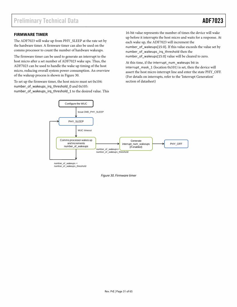
FIRMWARE TIMER The ADF7023 will wake up from PHY_SLEEP at the rate set by the hardware timer. A firmware timer can also be used on the comms processor to count the number of hardware wakeups.
The firmware timer can be used to generate an interrupt to the host micro after a set number of ADF7023 wake ups. Thus, the ADF7023 can be used to handle the wake up timing of the host micro, reducing overall system power consumption. An overview of the wakeup process is shown in Figure 30.
To set up the firmware timer, the host micro must set 0x104: number_of_wakeups_irq_threshold_0 and 0x105: number_of_wakeups_irq_threshold_1 to the desired value. This
16-bit value represents the number of times the device will wake up before it interrupts the host micro and waits for a response. At each wake up, the ADF7023 will increment the number_of_wakeups[15:0]. If this value exceeds the value set by number_of_wakeups_irq_threshold then the number_of_wakeups[15:0] value will be cleared to zero.
At this time, if the interrupt_num_wakeups bit in interrupt_mask_1 (location 0x101) is set, then the device will assert the host micro interrupt line and enter the state PHY_OFF. (For details on interrupts, refer to the ‘Interrupt Generation’ section of datasheet)
Figure 30. Firmware timer
Configure the WUC
PHY_SLEEP
Issue CMD_PHY_SLEEP
WUC timeout
Comms processor wakes upand increments
number_of_wakeupsnumber_of_wakeups>number_of_wakeups_threshold
number_of_wakeups <number_of_wakeups_threshold
PHY_OFFGenerate
interrupt_num_wakeups(if enabled)
Preliminary Technical Data ADF7023
Rev. PrE | Page 32 of 65
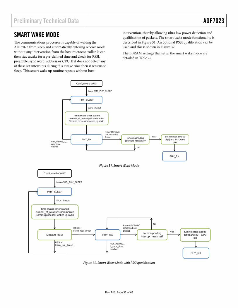
SMART WAKE MODE The communications processor is capable of waking the ADF7023 from sleep and automatically entering receive mode without any intervention from the host microcontroller. It can then stay awake for a pre-defined time and check for RSSI, preamble, sync word, address or CRC. If it does not detect any of these set interrupts during this awake time then it returns to sleep. This smart wake up routine repeats without host
intervention, thereby allowing ultra low power detection and qualification of packets. The smart wake mode functionality is described in Figure 31. An optional RSSI qualification can be used and this is shown in Figure 32.
The BBRAM settings that setup the smart wake mode are detailed in Table 22.
Figure 31. Smart Wake Mode
Figure 32. Smart Wake Mode with RSSI qualification
Configure the WUC
PHY_SLEEP
Issue CMD_PHY_SLEEP
WUC timeout
PHY_RX Is corresponding interrupt mask set?
Preamble/SWD/CRC/Address Detect Yes
No
Set interrupt source bit(s) and INT_GP3
pin
PHY_RX
max_wakeup_2_sync_time reached
Time awake timer startednumber_of_wakeups incrementedComms processor wakes up radio
Configure the WUC
PHY_SLEEP
Issue CMD_PHY_SLEEP
WUC timeout
Time awake timer startednumber_of_wakeups incrementedComms processor wakes up radio
Measure RSSI Is corresponding interrupt mask set?
Preamble/SWD/CRC/Address Detect Yes
No
Set interrupt source bit(s) and INT_GP3
pin
PHY_RX
max_wakeup_2_sync_time reached
RSSI < listen_rssi_thresh
RSSI > listen_rssi_thresh
PHY_RX
Preliminary Technical Data ADF7023
Rev. PrE | Page 33 of 65
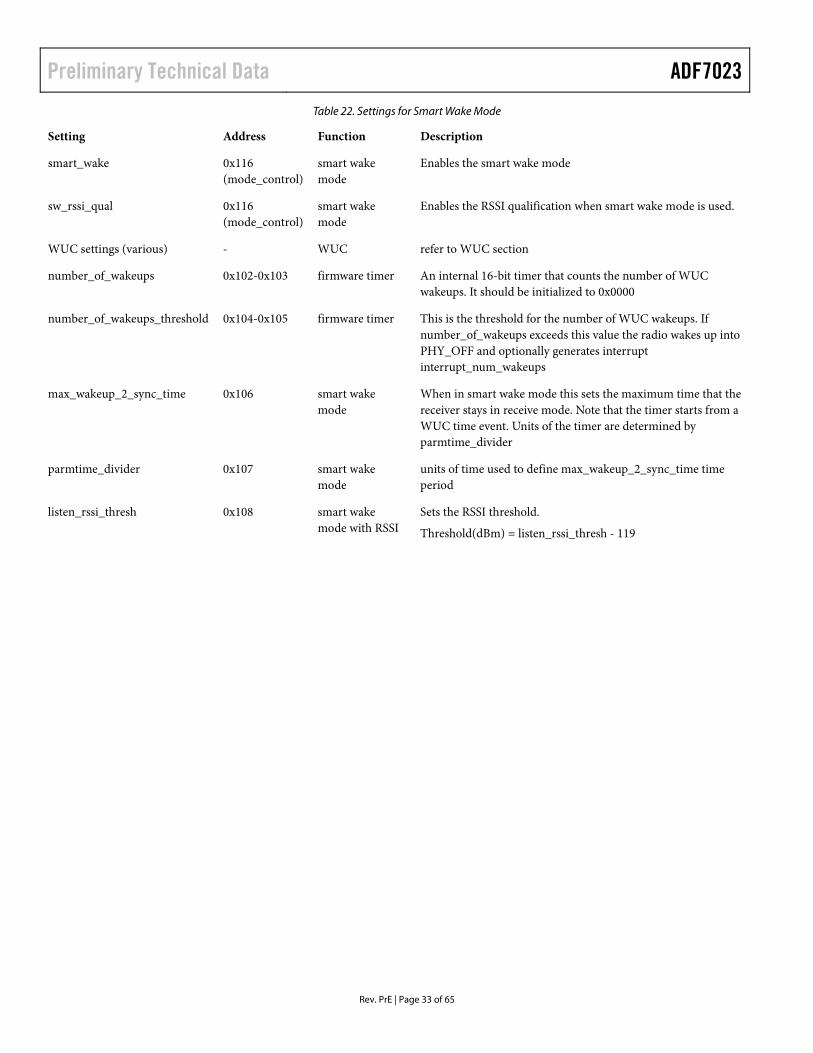
Table 22. Settings for Smart Wake Mode
Setting Address Function Description
smart_wake 0x116 (mode_control)
smart wake mode
Enables the smart wake mode
sw_rssi_qual 0x116 (mode_control)
smart wake mode
Enables the RSSI qualification when smart wake mode is used.
WUC settings (various) - WUC refer to WUC section
number_of_wakeups 0x102-0x103 firmware timer An internal 16-bit timer that counts the number of WUC wakeups. It should be initialized to 0x0000
number_of_wakeups_threshold 0x104-0x105 firmware timer This is the threshold for the number of WUC wakeups. If number_of_wakeups exceeds this value the radio wakes up into PHY_OFF and optionally generates interrupt interrupt_num_wakeups
max_wakeup_2_sync_time 0x106 smart wake mode
When in smart wake mode this sets the maximum time that the receiver stays in receive mode. Note that the timer starts from a WUC time event. Units of the timer are determined by parmtime_divider
parmtime_divider 0x107 smart wake mode
units of time used to define max_wakeup_2_sync_time time period
listen_rssi_thresh 0x108 smart wake mode with RSSI
Sets the RSSI threshold.
Threshold(dBm) = listen_rssi_thresh - 119
ADF7023 Preliminary Technical Data
Rev. PrE | Page 34 of 65
AES ENCRYPTION AND DECRYPTION ENGINE FUNCTIONALITY The basic functionality of 128 bit block encryption and decryption is supported with key sizes of 128, 192 and 256 bits.
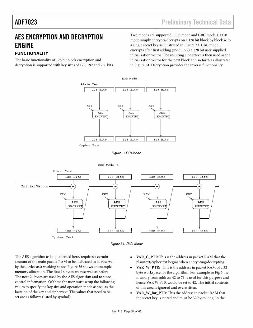
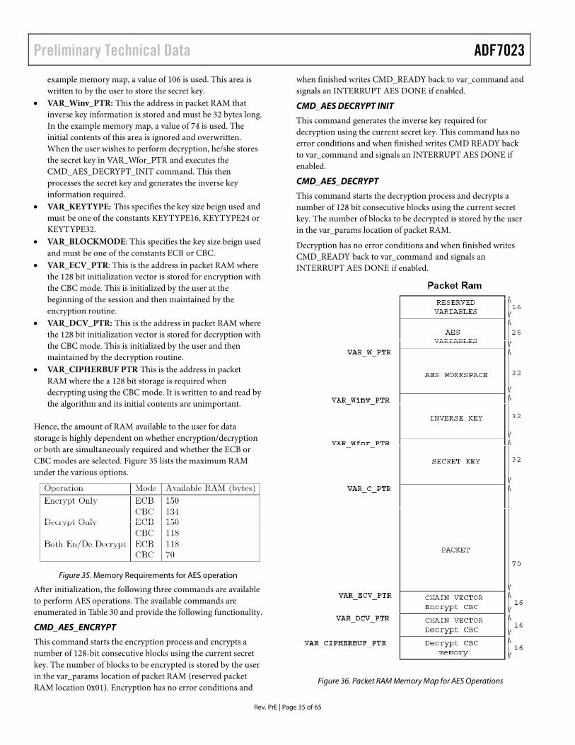
Two modes are supported, ECB mode and CBC mode 1. ECB mode simply encrypts/decrypts on a 128 bit block by block with a single secret key as illustrated in Figure 33. CBC mode 1 encrypts after first adding (modulo 2) a 128 bit user supplied initialization vector. The resulting ciphertext is then used as the initialization vector for the next block and so forth as illustrated in Figure 34. Decryption provides the inverse functionality.
Figure 33 ECB Mode.
Figure 34. CBC1 Mode
The AES algorithm as implemented here, requires a certain amount of the main packet RAM to be dedicated to be reserved by the device as a working space. Figure 36 shows an example memory allocation. The first 16 bytes are reserved as before. The next 24 bytes are used by the AES algorithm and to store control information. Of these the user must setup the following values to specify the key size and operation mode as well as the location of the key and ciphertext. The values that need to be set are as follows (listed by symbol):
• VAR_C_PTR:This is the address in packet RAM that the plaintext/ciphertext begins when encrypting/decrypting.
• VAR_W_PTR: This is the address in packet RAM of a 32 byte workspace for the algorithm. For example in Fig 6 the memory from address 42 to 73 is used for this purpose and hence VAR W PTR would be set to 42. The initial contents of this area is ignored and overwritten.
• VAR_W_for_PTR: This the address in packet RAM that the secret key is stored and must be 32 bytes long. In the
Preliminary Technical Data ADF7023
Rev. PrE | Page 35 of 65
example memory map, a value of 106 is used. This area is written to by the user to store the secret key.
• VAR_Winv_PTR: This the address in packet RAM that inverse key information is stored and must be 32 bytes long. In the example memory map, a value of 74 is used. The initial contents of this area is ignored and overwritten. When the user wishes to perform decryption, he/she stores the secret key in VAR_Wfor_PTR and executes the CMD_AES_DECRYPT_INIT command. This then processes the secret key and generates the inverse key information required.
• VAR_KEYTYPE: This specifies the key size beign used and must be one of the constants KEYTYPE16, KEYTYPE24 or KEYTYPE32.
• VAR_BLOCKMODE: This specifies the key size beign used and must be one of the constants ECB or CBC.
• VAR_ECV_PTR: This is the address in packet RAM where the 128 bit initialization vector is stored for encryption with the CBC mode. This is initialized by the user at the beginning of the session and then maintained by the encryption routine.
• VAR_DCV_PTR: This is the address in packet RAM where the 128 bit initialization vector is stored for decryption with the CBC mode. This is initialized by the user and then maintained by the decryption routine.
• VAR_CIPHERBUF PTR This is the address in packet RAM where the a 128 bit storage is required when decrypting using the CBC mode. It is written to and read by the algorithm and its initial contents are unimportant.
Hence, the amount of RAM available to the user for data storage is highly dependent on whether encryption/decryption or both are simultaneously required and whether the ECB or CBC modes are selected. Figure 35 lists the maximum RAM under the various options.
Figure 35. Memory Requirements for AES operation
After initialization, the following three commands are available to perform AES operations. The available commands are enumerated in Table 30 and provide the following functionality.
CMD_AES_ENCRYPT
This command starts the encryption process and encrypts a number of 128-bit consecutive blocks using the current secret key. The number of blocks to be encrypted is stored by the user in the var_params location of packet RAM (reserved packet RAM location 0x01). Encryption has no error conditions and
when finished writes CMD_READY back to var_command and signals an INTERRUPT AES DONE if enabled.
CMD_AES DECRYPT INIT
This command generates the inverse key required for decryption using the current secret key. This command has no error conditions and when finished writes CMD READY back to var_command and signals an INTERRUPT AES DONE if enabled.
CMD_AES_DECRYPT
This command starts the decryption process and decrypts a number of 128 bit consecutive blocks using the current secret key. The number of blocks to be decrypted is stored by the user in the var_params location of packet RAM.
Decryption has no error conditions and when finished writes CMD_READY back to var_command and signals an INTERRUPT AES DONE if enabled.
Figure 36. Packet RAM Memory Map for AES Operations
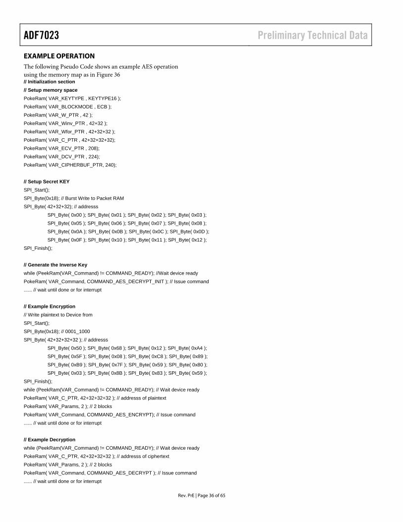
ADF7023 Preliminary Technical Data
Rev. PrE | Page 36 of 65
EXAMPLE OPERATION The following Pseudo Code shows an example AES operation using the memory map as in Figure 36// Initialization section // Setup memory space PokeRam( VAR_KEYTYPE , KEYTYPE16 );
PokeRam( VAR_BLOCKMODE , ECB );
PokeRam( VAR_W_PTR , 42 );
PokeRam( VAR_Winv_PTR , 42+32 );
PokeRam( VAR_Wfor_PTR , 42+32+32 );
PokeRam( VAR_C_PTR , 42+32+32+32);
PokeRam( VAR_ECV_PTR , 208);
PokeRam( VAR_DCV_PTR , 224);
PokeRam( VAR_CIPHERBUF_PTR, 240);
// Setup Secret KEY SPI_Start();
SPI_Byte(0x18); // Burst Write to Packet RAM
SPI_Byte( 42+32+32); // addresss
SPI_Byte( 0x00 ); SPI_Byte( 0x01 ); SPI_Byte( 0x02 ); SPI_Byte( 0x03 );
SPI_Byte( 0x05 ); SPI_Byte( 0x06 ); SPI_Byte( 0x07 ); SPI_Byte( 0x08 );
SPI_Byte( 0x0A ); SPI_Byte( 0x0B ); SPI_Byte( 0x0C ); SPI_Byte( 0x0D );
SPI_Byte( 0x0F ); SPI_Byte( 0x10 ); SPI_Byte( 0x11 ); SPI_Byte( 0x12 );
SPI_Finish();
// Generate the Inverse Key while (PeekRam(VAR_Command) != COMMAND_READY); //Wait device ready
PokeRam( VAR_Command, COMMAND_AES_DECRYPT_INIT ); // Issue command
...... // wait until done or for interrupt
// Example Encryption // Write plaintext to Device from
SPI_Start();
SPI_Byte(0x18); // 0001_1000
SPI_Byte( 42+32+32+32 ); // addresss
SPI_Byte( 0x50 ); SPI_Byte( 0x68 ); SPI_Byte( 0x12 ); SPI_Byte( 0xA4 );
SPI_Byte( 0x5F ); SPI_Byte( 0x08 ); SPI_Byte( 0xC8 ); SPI_Byte( 0x89 );
SPI_Byte( 0xB9 ); SPI_Byte( 0x7F ); SPI_Byte( 0x59 ); SPI_Byte( 0x80 );
SPI_Byte( 0x03 ); SPI_Byte( 0x8B ); SPI_Byte( 0x83 ); SPI_Byte( 0x59 );
SPI_Finish();
while (PeekRam(VAR_Command) != COMMAND_READY); // Wait device ready
PokeRam( VAR_C_PTR, 42+32+32+32 ); // addresss of plaintext
PokeRam( VAR_Params, 2 ); // 2 blocks
PokeRam( VAR_Command, COMMAND_AES_ENCRYPT); // Issue command
...... // wait until done or for interrupt
// Example Decryption while (PeekRam(VAR_Command) != COMMAND_READY); // Wait device ready
PokeRam( VAR_C_PTR, 42+32+32+32 ); // addresss of ciphertext
PokeRam( VAR_Params, 2 ); // 2 blocks
PokeRam( VAR_Command, COMMAND_AES_DECRYPT ); // Issue command
...... // wait until done or for interrupt
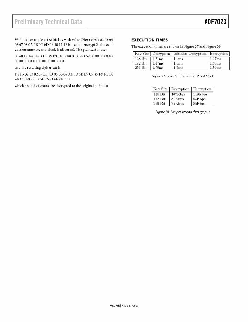
Preliminary Technical Data ADF7023
Rev. PrE | Page 37 of 65
With this example a 128 bit key with value (Hex) 00 01 02 03 05 06 07 08 0A 0B 0C 0D 0F 10 11 12 is used to encrypt 2 blocks of data (assume second block is all zeros). The plaintext is then:
50 68 12 A4 5F 08 C8 89 B9 7F 59 80 03 8B 83 59 00 00 00 00 00 00 00 00 00 00 00 00 00 00 00 00
and the resulting ciphertext is
D8 F5 32 53 82 89 EF 7D 06 B5 06 A4 FD 5B E9 C9 85 F9 FC E0 A8 CC F9 72 F9 5F 76 83 6F 9F FF F5
which should of course be decrypted to the original plaintext.
EXECUTION TIMES The execution times are shown in Figure 37 and Figure 38.
Figure 37. Execution Times for 128 bit block
Figure 38. Bits per second throughput
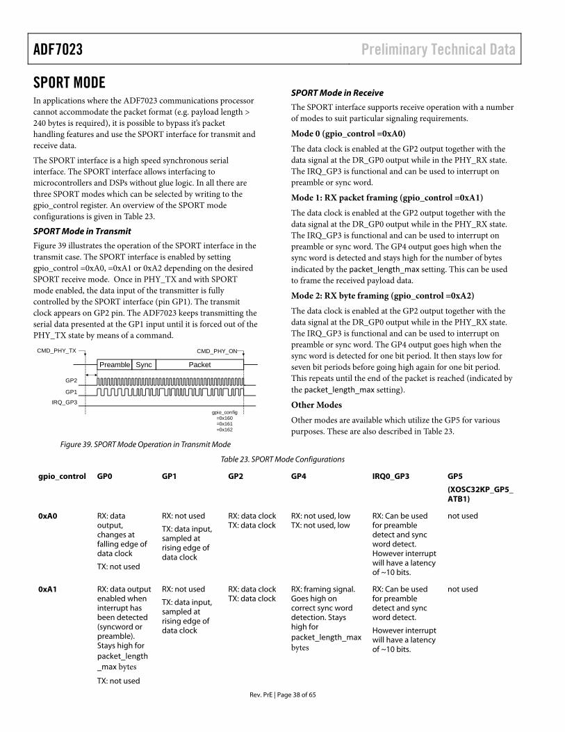
ADF7023 Preliminary Technical Data
Rev. PrE | Page 38 of 65
SPORT MODE In applications where the ADF7023 communications processor cannot accommodate the packet format (e.g. payload length > 240 bytes is required), it is possible to bypass it’s packet handling features and use the SPORT interface for transmit and receive data.
The SPORT interface is a high speed synchronous serial interface. The SPORT interface allows interfacing to microcontrollers and DSPs without glue logic. In all there are three SPORT modes which can be selected by writing to the gpio_control register. An overview of the SPORT mode configurations is given in Table 23.
SPORT Mode in Transmit
Figure 39 illustrates the operation of the SPORT interface in the transmit case. The SPORT interface is enabled by setting gpio_control =0xA0, =0xA1 or 0xA2 depending on the desired SPORT receive mode. Once in PHY_TX and with SPORT mode enabled, the data input of the transmitter is fully controlled by the SPORT interface (pin GP1). The transmit clock appears on GP2 pin. The ADF7023 keeps transmitting the serial data presented at the GP1 input until it is forced out of the PHY_TX state by means of a command.
Figure 39. SPORT Mode Operation in Transmit Mode
SPORT Mode in Receive
The SPORT interface supports receive operation with a number of modes to suit particular signaling requirements.
Mode 0 (gpio_control =0xA0)
The data clock is enabled at the GP2 output together with the data signal at the DR_GP0 output while in the PHY_RX state. The IRQ_GP3 is functional and can be used to interrupt on preamble or sync word.
Mode 1: RX packet framing (gpio_control =0xA1)
The data clock is enabled at the GP2 output together with the data signal at the DR_GP0 output while in the PHY_RX state. The IRQ_GP3 is functional and can be used to interrupt on preamble or sync word. The GP4 output goes high when the sync word is detected and stays high for the number of bytes indicated by the packet_length_max setting. This can be used to frame the received payload data.
Mode 2: RX byte framing (gpio_control =0xA2)
The data clock is enabled at the GP2 output together with the data signal at the DR_GP0 output while in the PHY_RX state. The IRQ_GP3 is functional and can be used to interrupt on preamble or sync word. The GP4 output goes high when the sync word is detected for one bit period. It then stays low for seven bit periods before going high again for one bit period. This repeats until the end of the packet is reached (indicated by the packet_length_max setting).
Other Modes
Other modes are available which utilize the GP5 for various purposes. These are also described in Table 23.
Table 23. SPORT Mode Configurations
gpio_control GP0 GP1 GP2 GP4 IRQ0_GP3 GP5
(XOSC32KP_GP5_ATB1)
0xA0 RX: data output, changes at falling edge of data clock
TX: not used
RX: not used
TX: data input, sampled at rising edge of data clock
RX: data clock TX: data clock
RX: not used, low TX: not used, low
RX: Can be used for preamble detect and sync word detect. However interrupt will have a latency of ~10 bits.
not used
0xA1 RX: data output enabled when interrupt has been detected (syncword or preamble). Stays high for packet_length_max bytes
TX: not used
RX: not used
TX: data input, sampled at rising edge of data clock
RX: data clock TX: data clock
RX: framing signal. Goes high on correct sync word detection. Stays high for packet_length_max bytes
RX: Can be used for preamble detect and sync word detect.
However interrupt will have a latency of ~10 bits.
not used
Preamble Sync Packet
GP2
GP1
IRQ_GP3
CMD_PHY_TX CMD_PHY_ON
gpio_config=0x160=0x161=0x162
Preliminary Technical Data ADF7023
Rev. PrE | Page 39 of 65
0xA2 RX: data output enabled when interrupt has been detected (syncword or preamble). Stays high for packet_length_max bytes
TX: not used
RX: not used
TX: data input, sampled at rising edge of data clock
RX: data clock TX: data clock
RX: strobe signal. Goes high for one bit period on the first bit of each byte after the sync word has been detected. Continues for packet_length_max bytes
RX: Can be used for preamble detect and sync word detect.
However interrupt will have a latency of ~10 bits.
not used
0xA3 same as 0xA0 32.768kHz crystal input on GP5
0xA4 same as 0xA1 32.768kHz crystal input on GP5
0xA5 same as 0xA2 32.768kHz crystal input on GP5
0xA6 same as 0xA0 ext_uc_clk signal output
0xA7 same as 0xA1 ext_uc_clk signal
output
0xA8 same as 0xA2 ext_uc_clk signal
output
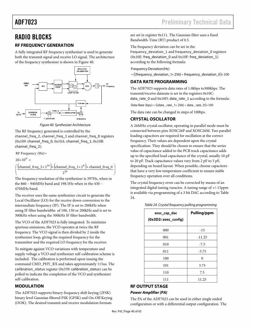
ADF7023 Preliminary Technical Data
Rev. PrE | Page 40 of 65
RADIO BLOCKS
RF FREQUENCY GENERATION A fully integrated RF frequency synthesizer is used to generate both the transmit signal and receive LO signal. The architecture of the frequency synthesizer is shown in Figure 40.
Figure 40. Synthesizer Architecture
The RF frequency generated is controlled by the channel_freq_2, channel_freq_1 and channel_freq_0 registers (0x109: channel_freq_0, 0x10A: channel_freq_1, 0x10B: channel_freq_2).
( ) ( )⎟⎟⎠
⎞⎜⎜⎝
⎛ +×+×
××
=
16
816
2eq_0channel_fr 2eq_1channel_fr2eq_2channel_fr
2
(Hz) FrequencyRF6106
The frequency resolution of the synthesizer is 397Hz, when in the 860 – 940MHz band and 198.5Hz when in the 430 – 470MHz band.
The receiver uses the same synthesizer circuit to generate the Local Oscillator (LO) for the receive down-conversion to the intermediate frequency (IF). The IF is set to 200kHz when using IF filter bandwidths of 100, 150 or 200kHz and is set to 300kHz when using the 300kHz IF filter bandwidth.
The VCO of the ADF7023 is fully integrated. To minimize spurious emissions, the VCO operates at twice the RF frequency. The VCO signal is then divided by 2 inside the synthesizer loop, giving the required frequency for the transmitter and the required LO frequency for the receiver.
To mitigate against VCO variations with temperature and supply voltage a VCO and synthesizer self-calibration scheme is included. The calibration is performed upon issuing the command CMD_PHY_RX and takes approximately 115us. The calibration_status register (0x339: calibration_status) can be polled to indicate the completion of the VCO and synthesizer self-calibration.
MODULATION The ADF7023 supports binary frequency shift keying (2FSK) binary level Gaussian filtered FSK (GFSK) and On-Off Keying (OOK). The desired transmit and receive modulation formats
are set in register 0x111. The Gaussian filter uses a fixed Bandwidth-Time (BT) product of 0.5.
The frequency deviation can be set in the frequency_deviation_1 and frequency_deviation_0 registers (0x10E: freq_deviation_0 and 0x10F: freq_deviation_1) according to the following formula:
( ) 100×+×= 0deviation_frequency_256)1deviation_frequency_(
)Hz(DeviationFrequency
DATA RATE PROGRAMMING The ADF7023 supports data rates of 1.0kbps to300kbps. The transmit/receive datarate is set in the registers 0x10C: data_rate_0 and 0x10D: data_rate_1 according to the formula:
( ) 100×+×= _0rate_atad256)_1rate_atad()bps(RateData
The data rate can be changed in steps of 100bps.
CRYSTAL OSCILLATOR A 26MHz crystal oscillator, operating in parallel mode must be connected between pins XOSC26P and XOSC26M. Two parallel loading capacitors are required for oscillation at the correct frequency. Their values are dependent upon the crystal specification. They should be chosen to ensure that the series value of capacitance added to the PCB track capacitance adds up to the specified load capacitance of the crystal, usually 10 pF to 20 pF. Track capacitance values vary from 2 pF to 5 pF, depending on board layout. When possible, choose capacitors that have a very low temperature coefficient to ensure stable frequency operation over all conditions.
The crystal frequency error can be corrected by means of an integrated digital tuning varactor. A tuning range of +/-15ppm is available via programming of a 3 bit DAC according to Table 24.
Table 24. Crystal frequency pulling programming
xosc_cap_dac
(0x3D2: xosc_config)
Pulling/ppm
000 -15
001 -11.25
010 -7.5
011 -3.75
100 0
101 3.75
110 7.5
111 11.25
RF OUTPUT STAGE Power Amplifier (PA)
The PA of the ADF7023 can be used in either single ended configuration or with a differential output configuration. The
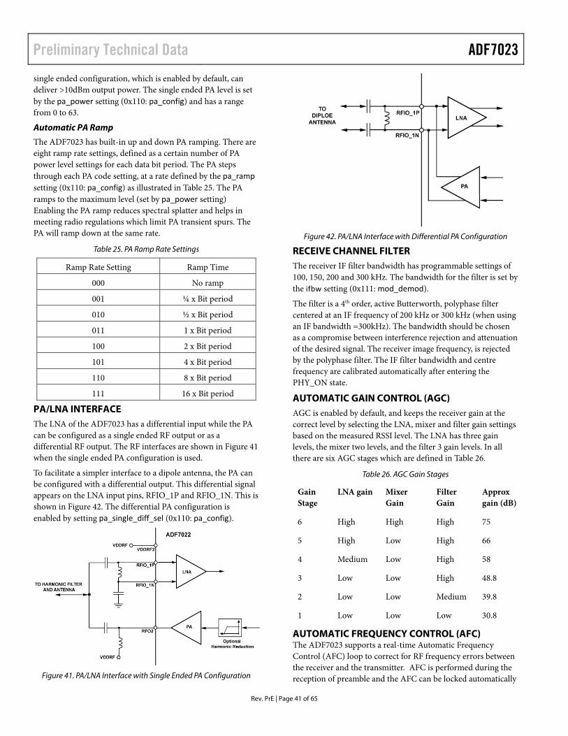
Preliminary Technical Data ADF7023
Rev. PrE | Page 41 of 65
single ended configuration, which is enabled by default, can deliver >10dBm output power. The single ended PA level is set by the pa_power setting (0x110: pa_config) and has a range from 0 to 63.
Automatic PA Ramp
The ADF7023 has built-in up and down PA ramping. There are eight ramp rate settings, defined as a certain number of PA power level settings for each data bit period. The PA steps through each PA code setting, at a rate defined by the pa_ramp setting (0x110: pa_config) as illustrated in Table 25. The PA ramps to the maximum level (set by pa_power setting) Enabling the PA ramp reduces spectral splatter and helps in meeting radio regulations which limit PA transient spurs. The PA will ramp down at the same rate.
Table 25. PA Ramp Rate Settings
Ramp Rate Setting Ramp Time
000 No ramp
001 ¼ x Bit period
010 ½ x Bit period
011 1 x Bit period
100 2 x Bit period
101 4 x Bit period
110 8 x Bit period
111 16 x Bit period
PA/LNA INTERFACE The LNA of the ADF7023 has a differential input while the PA can be configured as a single ended RF output or as a differential RF output. The RF interfaces are shown in Figure 41 when the single ended PA configuration is used.
To facilitate a simpler interface to a dipole antenna, the PA can be configured with a differential output. This differential signal appears on the LNA input pins, RFIO_1P and RFIO_1N. This is shown in Figure 42. The differential PA configuration is enabled by setting pa_single_diff_sel (0x110: pa_config).
Figure 41. PA/LNA Interface with Single Ended PA Configuration
Figure 42. PA/LNA Interface with Differential PA Configuration
RECEIVE CHANNEL FILTER The receiver IF filter bandwidth has programmable settings of 100, 150, 200 and 300 kHz. The bandwidth for the filter is set by the ifbw setting (0x111: mod_demod).
The filter is a 4th order, active Butterworth, polyphase filter centered at an IF frequency of 200 kHz or 300 kHz (when using an IF bandwidth =300kHz). The bandwidth should be chosen as a compromise between interference rejection and attenuation of the desired signal. The receiver image frequency, is rejected by the polyphase filter. The IF filter bandwidth and centre frequency are calibrated automatically after entering the PHY_ON state.
AUTOMATIC GAIN CONTROL (AGC) AGC is enabled by default, and keeps the receiver gain at the correct level by selecting the LNA, mixer and filter gain settings based on the measured RSSI level. The LNA has three gain levels, the mixer two levels, and the filter 3 gain levels. In all there are six AGC stages which are defined in Table 26.
Table 26. AGC Gain Stages
Gain Stage
LNA gain Mixer Gain
Filter Gain
Approx gain (dB)
6 High High High 75
5 High Low High 66
4 Medium Low High 58
3 Low Low High 48.8
2 Low Low Medium 39.8
1 Low Low Low 30.8
AUTOMATIC FREQUENCY CONTROL (AFC) The ADF7023 supports a real-time Automatic Frequency Control (AFC) loop to correct for RF frequency errors between the receiver and the transmitter. AFC is performed during the reception of preamble and the AFC can be locked automatically
ADF7023 Preliminary Technical Data
Rev. PrE | Page 42 of 65
on reception of SWD. The AFC pull-in-range is the maximum frequency ±range programmable. The ADF7023 can be configured in one of two modes to support AFC. These are detailed in Table 27. The AFC can be locked on a valid SWD reception or else left free running in which case the AFC will be enabled for the entire packet. These settings are described in Table 28.
Table 27. AFC Modes
Mode afc_scheme (0x112, afc_mode)
Mode1 10b Mode 2 01b
Table 28. Description of afc_lock_mode register settings
afc_lock_mode (0x112, afc_mode)
AFC Lock Mode
00 Free Running: AFC is free running 01 Disabled: AFC is disabled 10 Hold AFC: AFC is paused 11 Lock: AFC locks on valid SWD
Mode 1 AFC
In the Mode 1 method a control loop adjusts the receiver’s LO frequency to remove the frequency error between the incoming packet and the receivers LO frequency. This frequency correction method also centers the received spectrum in middle of the baseband IF filter. The ADF7023 is capable of measuring measure frequency errors, performing AGC and obtaining bit synchronization within 4 bytes of preamble. However, depending on the mode of AFC selected, there will be some differences in both the AFC pull-in range and the number of preamble bits required in both correction schemes. This is summarized in Table 29.
Mode 2 AFC
In the Mode 2 AFC scheme a control loop adjusts the FSK demodulator’s response such that it can optimally demodulate the incoming packet while accommodating the frequency error. The local oscillator frequency is not changed in this mode, so it is possible, with large frequency errors, that the received signal will be close to, or outside the IF filter bandwidth, which would degrade receiver sensitivity.
Table 29. Comparison of the two AFC Methods
Mode 1 Mode 2 Minimum Preamble Length
35 bits 28 bits
AFC Pull-in Range (0x315: max_afc_range)
(programmable) up to 100kHz
(programmable) up to 40kHz
Adjustment Local oscillator (IF frequency centred)
Demod (IF frequency not centred)
RSSI The RSSI is implemented as a successive compression log amp following the baseband channel filtering.
The RSSI level is converted for user readback and digitally controlled AGC by an (8-bit) SAR ADC. Ths value can be read from rssi_readback (0x312) The rssi_usr_out is a 2s complement binary value and can be converted to input power in dBm using the formula:
Input Power (dBm) = rssi_usr_out - 119
The RSSI is also used for on-off keying (OOK) demodulation.
IMAGE REJECTION CALIBRATION The image channel in the ADF7023 is 2x the IF frequency below the desired signal. When using an IF filter bandwidth of 100, 150 or 200kHz the image frequency is 400kHz below the desired signal and when using the 300kHz IF filter bandwidth the image channel is 600kHz below the desired signal (as an IF frequency of 300kHz is used with that IF filter bandwidth). The polyphase filter rejects this image with an asymmetric frequency response. The image rejection performance of the receiver is dependent on how well matched the I and Q signals are in amplitude, and how well matched the quadrature is between them (that is, how close to 90° apart they are). The uncalibrated image rejection performance is approximately 30 dB (at 868 MHz). However, it is possible to improve on this performance by as much as 20 dB by finding the optimum I/Q gain and phase adjust settings.
RF Source
To perform a calibration of the I/Q gain and phase, an RF source centered at the image frequency is required. This can either be an external RF source an internally generated RF source of the ADF7023.
Calibration Routine
With an RF signal centered at the image frequency, an RSSI readback is performed for each gain and phase adjust setting. The optimum point is the gain and phase adjust setting that corresponds to the lowest RSSI readback (i.e. providing the greatest rejection of the image signal).
The simplest (but obviously longest) calibration involves searching every possible combination of gain and phase adjust to find the optimum. The alternative is to use an intelligent search algorithm which will find the optimum point in a more efficient manner. Analog Devices provide such a calibration routine in software code that can be downloaded to the ADF7023. Please contact Analog Devices for further information.
Preliminary Technical Data ADF7023
Rev. PrE | Page 43 of 65
PERIPHERAL FEATURES ANALOG TO DIGITAL CONVERTER The ADF7023 supports an integrated SAR ADC for digitization of analog signals that include the analog temperature sensor, the analog RSSI level and an external analog input signal (Pin 30).
The result of the conversion can be read from registers 0x327: adc_readback_high and 0x328: adc_readback_low.
The integrated temperature sensor has an operating range between -40°C and 70°C. With the ADC operating at 10 bits of resolution, the resolution of the temperature sensor is 0.2°C. When uncalibrated the temperature sensor is accurate to ±11°C at 25°C.
BATTERY MONITOR TBD
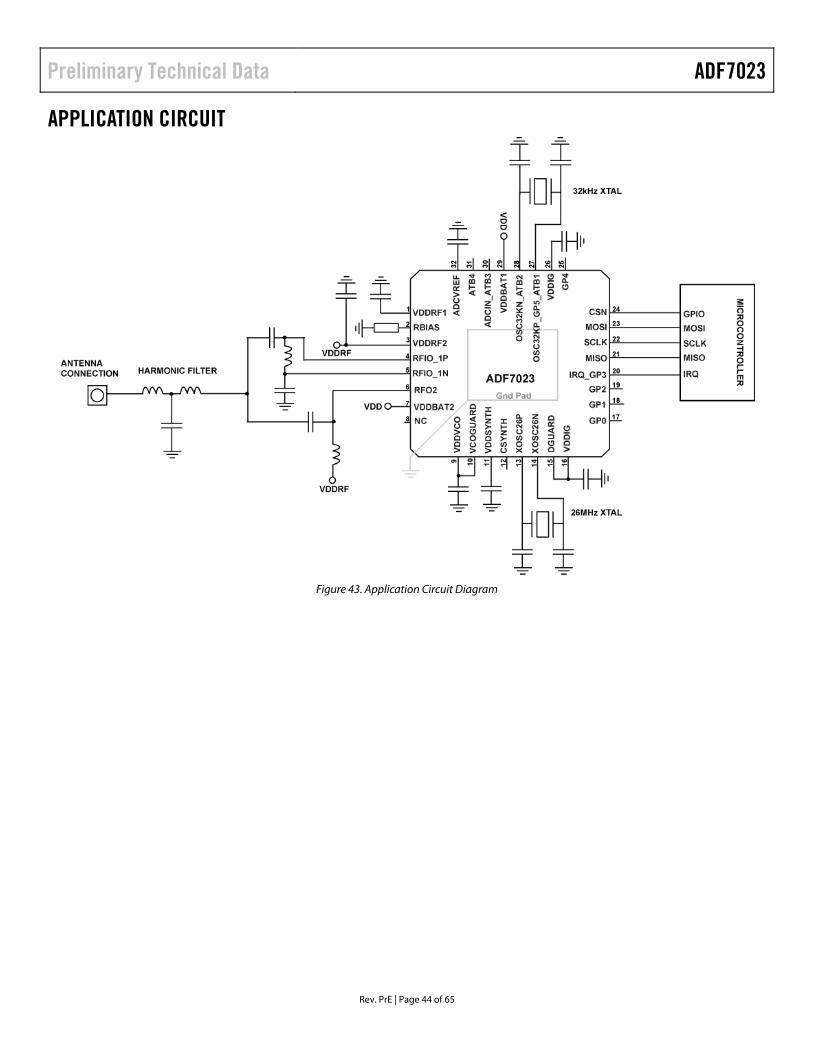
Preliminary Technical Data ADF7023
Rev. PrE | Page 44 of 65
APPLICATION CIRCUIT
Figure 43. Application Circuit Diagram
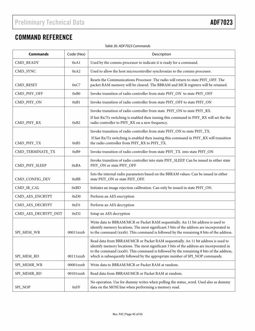
Preliminary Technical Data ADF7023
Rev. PrE | Page 45 of 65
COMMAND REFERENCE Table 30. ADF7023 Commands
Commands Code (Hex) Description
CMD_READY 0xA1 Used by the comms processor to indicate it is ready for a command.
CMD_SYNC 0xA2 Used to allow the host microcontroller synchronize to the comms processor.
CMD_RESET 0xC7 Resets the Communications Processor. The radio will return to state PHY_OFF. The packet RAM memory will be cleared. The BBRAM and MCR registers will be retained.
CMD_PHY_OFF 0xB0 Invoke transition of radio controller from state PHY_ON to state PHY_OFF
CMD_PHY_ON 0xB1 Invoke transition of radio controller from state PHY_OFF to state PHY_ON
CMD_PHY_RX 0xB2
Invoke transition of radio controller from state PHY_ON to state PHY_RX.
If fast Rx/Tx switching is enabled then issuing this command in PHY_RX will set the the radio controller to PHY_RX on a new frequency.
CMD_PHY_TX 0xB5
Invoke transition of radio controller from state PHY_ON to state PHY_TX.
If fast Rx/Tx switching is enabled then issuing this command in PHY_RX will transition the radio controller from PHY_RX to PHY_TX.
CMD_TERMINATE_TX 0xB9 Invoke transition of radio controller from state PHY_TX into state PHY_ON
CMD_PHY_SLEEP 0xBA Invoke transition of radio controller into state PHY_SLEEP. Can be issued in either state PHY_ON or state PHY_OFF
CMD_CONFIG_DEV 0xBB Sets the internal radio parameters based on the BBRAM values. Can be issued in either state PHY_ON or state PHY_OFF.
CMD_IR_CAL 0xBD Initiates an image rejection calibration. Can only be issued in state PHY_ON.
CMD_AES_ENCRYPT 0xD0 Perform an AES encryption
CMD_AES_DECRYPT 0xD1 Perform an AES decryption
CMD_AES_DECRYPT_INIT 0xD2 Setup an AES decryption
SPI_MEM_WR 00011xxxb
Write data to BBRAM/MCR or Packet RAM sequentially. An 11 bit address is used to identify memory locations. The most significant 3 bits of the address are incorporated in to the command (xxxb). This command is followed by the remaining 8 bits of the address.
SPI_MEM_RD 00111xxxb
Read data from BBRAM/MCR or Packet RAM sequentially. An 11 bit address is used to identify memory locations. The most significant 3 bits of the address are incorporated in to the command (xxxb). This command is followed by the remaining 8 bits of the address, which is subsequently followed by the appropriate number of SPI_NOP commands.
SPI_MEMR_WR 00001xxxb Write data to BBRAM/MCR or Packet RAM at random.
SPI_MEMR_RD 00101xxxb Read data from BBRAM/MCR or Packet RAM at random.
SPI_NOP 0xFF No operation. Use for dummy writes when polling the status_word. Used also as dummy data on the MOSI line when performing a memory read.
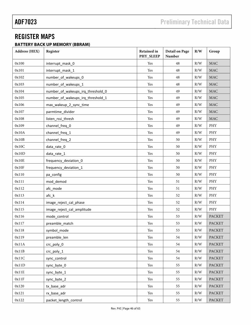
ADF7023 Preliminary Technical Data
Rev. PrE | Page 46 of 65
REGISTER MAPS BATTERY BACK UP MEMORY (BBRAM)
Address (HEX) Register Retained in PHY_SLEEP
Detail on Page Number
R/W Group
0x100 interrupt_mask_0 Yes 48 R/W MAC
0x101 interrupt_mask_1 Yes 48 R/W MAC
0x102 number_of_wakeups_0 Yes 48 R/W MAC
0x103 number_of_wakeups_1 Yes 48 R/W MAC
0x104 number_of_wakeups_irq_threshold_0 Yes 49 R/W MAC
0x105 number_of_wakeups_irq_threshold_1 Yes 49 R/W MAC
0x106 max_wakeup_2_sync_time Yes 49 R/W MAC
0x107 parmtime_divider Yes 49 R/W MAC
0x108 listen_rssi_thresh Yes 49 R/W MAC
0x109 channel_freq_0 Yes 49 R/W PHY
0x10A channel_freq_1 Yes 49 R/W PHY
0x10B channel_freq_2 Yes 50 R/W PHY
0x10C data_rate_0 Yes 50 R/W PHY
0x10D data_rate_1 Yes 50 R/W PHY
0x10E frequency_deviation_0 Yes 50 R/W PHY
0x10F frequency_deviation_1 Yes 50 R/W PHY
0x110 pa_config Yes 50 R/W PHY
0x111 mod_demod Yes 51 R/W PHY
0x112 afc_mode Yes 51 R/W PHY
0x113 afc_k Yes 52 R/W PHY
0x114 image_reject_cal_phase Yes 52 R/W PHY
0x115 image_reject_cal_amplitude Yes 52 R/W PHY
0x116 mode_control Yes 53 R/W PACKET
0x117 preamble_match Yes 53 R/W PACKET
0x118 symbol_mode Yes 53 R/W PACKET
0x119 preamble_len Yes 54 R/W PACKET
0x11A crc_poly_0 Yes 54 R/W PACKET
0x11B crc_poly_1 Yes 54 R/W PACKET
0x11C sync_control Yes 54 R/W PACKET
0x11D sync_byte_0 Yes 55 R/W PACKET
0x11E sync_byte_1 Yes 55 R/W PACKET
0x11F sync_byte_2 Yes 55 R/W PACKET
0x120 tx_base_adr Yes 55 R/W PACKET
0x121 rx_base_adr Yes 55 R/W PACKET
0x122 packet_length_control Yes 55 R/W PACKET
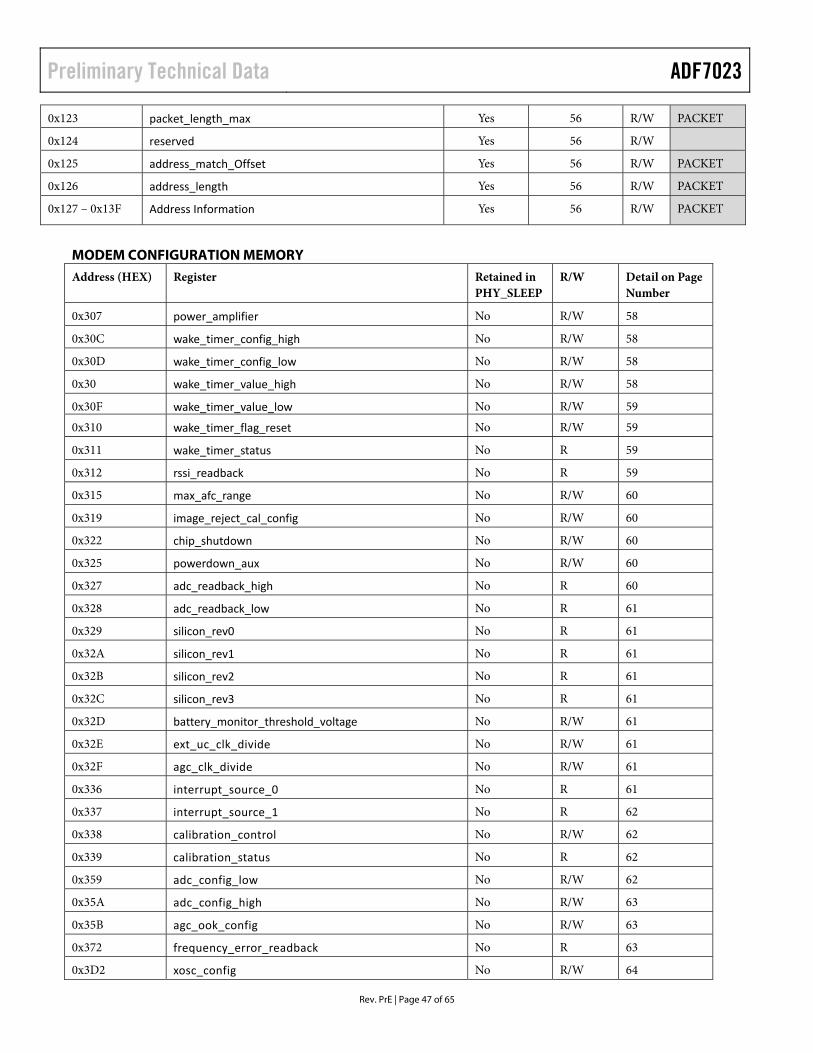
Preliminary Technical Data ADF7023
Rev. PrE | Page 47 of 65
0x123 packet_length_max Yes 56 R/W PACKET
0x124 reserved Yes 56 R/W
0x125 address_match_Offset Yes 56 R/W PACKET
0x126 address_length Yes 56 R/W PACKET
0x127 – 0x13F Address Information Yes 56 R/W PACKET
MODEM CONFIGURATION MEMORY
Address (HEX) Register Retained in PHY_SLEEP
R/W Detail on Page Number
0x307 power_amplifier No R/W 58
0x30C wake_timer_config_high No R/W 58
0x30D wake_timer_config_low No R/W 58
0x30 wake_timer_value_high No R/W 58
0x30F wake_timer_value_low No R/W 59
0x310 wake_timer_flag_reset No R/W 59
0x311 wake_timer_status No R 59
0x312 rssi_readback No R 59
0x315 max_afc_range No R/W 60
0x319 image_reject_cal_config No R/W 60
0x322 chip_shutdown No R/W 60
0x325 powerdown_aux No R/W 60
0x327 adc_readback_high No R 60
0x328 adc_readback_low No R 61
0x329 silicon_rev0 No R 61
0x32A silicon_rev1 No R 61
0x32B silicon_rev2 No R 61
0x32C silicon_rev3 No R 61
0x32D battery_monitor_threshold_voltage No R/W 61
0x32E ext_uc_clk_divide No R/W 61
0x32F agc_clk_divide No R/W 61
0x336 interrupt_source_0 No R 61
0x337 interrupt_source_1 No R 62
0x338 calibration_control No R/W 62
0x339 calibration_status No R 62
0x359 adc_config_low No R/W 62
0x35A adc_config_high No R/W 63
0x35B agc_ook_config No R/W 63
0x372 frequency_error_readback No R 63
0x3D2 xosc_config No R/W 64
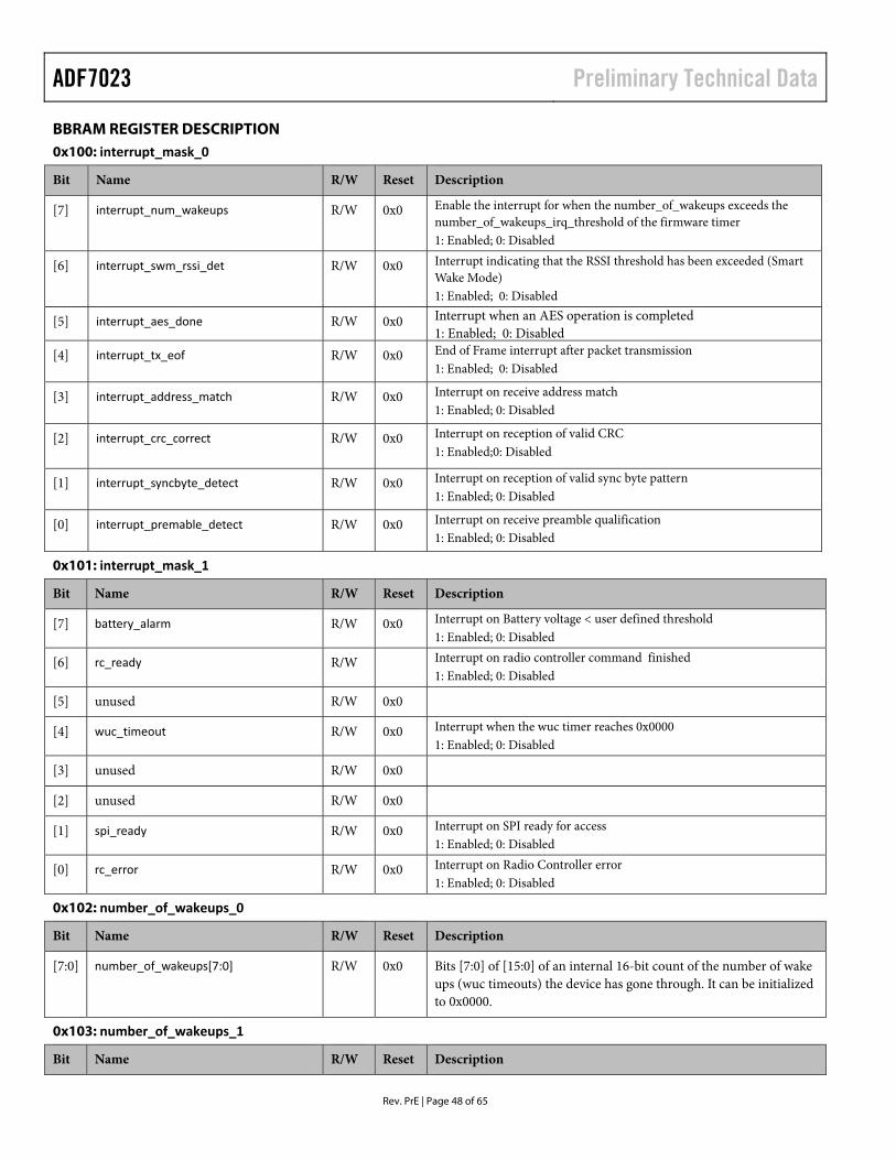
ADF7023 Preliminary Technical Data
Rev. PrE | Page 48 of 65
BBRAM REGISTER DESCRIPTION 0x100: interrupt_mask_0
Bit Name R/W Reset Description
[7] interrupt_num_wakeups R/W 0x0 Enable the interrupt for when the number_of_wakeups exceeds the number_of_wakeups_irq_threshold of the firmware timer 1: Enabled; 0: Disabled
[6] interrupt_swm_rssi_det R/W 0x0 Interrupt indicating that the RSSI threshold has been exceeded (Smart Wake Mode) 1: Enabled; 0: Disabled
[5] interrupt_aes_done R/W 0x0 Interrupt when an AES operation is completed 1: Enabled; 0: Disabled
[4] interrupt_tx_eof R/W 0x0 End of Frame interrupt after packet transmission 1: Enabled; 0: Disabled
[3] interrupt_address_match R/W 0x0 Interrupt on receive address match 1: Enabled; 0: Disabled
[2] interrupt_crc_correct R/W 0x0 Interrupt on reception of valid CRC 1: Enabled;0: Disabled
[1] interrupt_syncbyte_detect R/W 0x0 Interrupt on reception of valid sync byte pattern 1: Enabled; 0: Disabled
[0] interrupt_premable_detect R/W 0x0 Interrupt on receive preamble qualification 1: Enabled; 0: Disabled
0x101: interrupt_mask_1
Bit Name R/W Reset Description
[7] battery_alarm R/W 0x0 Interrupt on Battery voltage < user defined threshold 1: Enabled; 0: Disabled
[6] rc_ready R/W Interrupt on radio controller command finished 1: Enabled; 0: Disabled
[5] unused R/W 0x0
[4] wuc_timeout R/W 0x0 Interrupt when the wuc timer reaches 0x0000 1: Enabled; 0: Disabled
[3] unused R/W 0x0
[2] unused R/W 0x0
[1] spi_ready R/W 0x0 Interrupt on SPI ready for access 1: Enabled; 0: Disabled
[0] rc_error R/W 0x0 Interrupt on Radio Controller error 1: Enabled; 0: Disabled
0x102: number_of_wakeups_0
Bit Name R/W Reset Description
[7:0] number_of_wakeups[7:0] R/W 0x0 Bits [7:0] of [15:0] of an internal 16-bit count of the number of wake ups (wuc timeouts) the device has gone through. It can be initialized to 0x0000.
0x103: number_of_wakeups_1
Bit Name R/W Reset Description
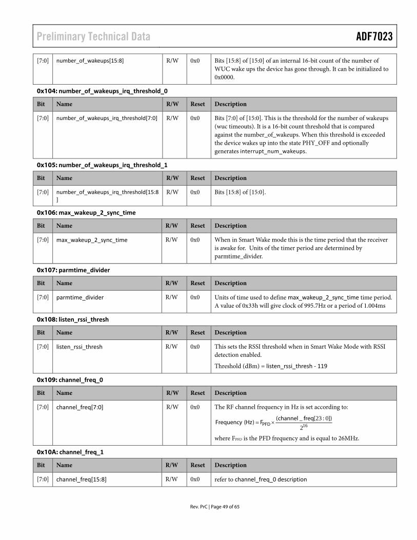
Preliminary Technical Data ADF7023
Rev. PrC | Page 49 of 65
[7:0] number_of_wakeups[15:8] R/W 0x0 Bits [15:8] of [15:0] of an internal 16-bit count of the number of WUC wake ups the device has gone through. It can be initialized to 0x0000.
0x104: number_of_wakeups_irq_threshold_0
Bit Name R/W Reset Description
[7:0] number_of_wakeups_irq_threshold[7:0] R/W 0x0 Bits [7:0] of [15:0]. This is the threshold for the number of wakeups (wuc timeouts). It is a 16-bit count threshold that is compared against the number_of_wakeups. When this threshold is exceeded the device wakes up into the state PHY_OFF and optionally generates interrupt_num_wakeups.
0x105: number_of_wakeups_irq_threshold_1
Bit Name R/W Reset Description
[7:0] number_of_wakeups_irq_threshold[15:8]
R/W 0x0 Bits [15:8] of [15:0].
0x106: max_wakeup_2_sync_time
Bit Name R/W Reset Description
[7:0] max_wakeup_2_sync_time R/W 0x0 When in Smart Wake mode this is the time period that the receiver is awake for. Units of the timer period are determined by parmtime_divider.
0x107: parmtime_divider
Bit Name R/W Reset Description
[7:0] parmtime_divider R/W 0x0 Units of time used to define max_wakeup_2_sync_time time period. A value of 0x33h will give clock of 995.7Hz or a period of 1.004ms
0x108: listen_rssi_thresh
Bit Name R/W Reset Description
[7:0] listen_rssi_thresh R/W 0x0 This sets the RSSI threshold when in Smart Wake Mode with RSSI detection enabled.
Threshold (dBm) = listen_rssi_thresh ‐ 119
0x109: channel_freq_0
Bit Name R/W Reset Description
[7:0] channel_freq[7:0] R/W 0x0 The RF channel frequency in Hz is set according to:
162023 ]):[freq_channel(
F)Hz(Frequency PFD ×=
where FPFD is the PFD frequency and is equal to 26MHz.
0x10A: channel_freq_1
Bit Name R/W Reset Description
[7:0] channel_freq[15:8] R/W 0x0 refer to channel_freq_0 description
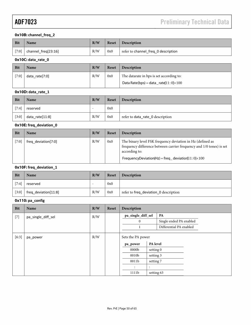
ADF7023 Preliminary Technical Data
Rev. PrE | Page 50 of 65
0x10B: channel_freq_2
Bit Name R/W Reset Description
[7:0] channel_freq[23:16] R/W 0x0 refer to channel_freq_0 description
0x10C: data_rate_0
Bit Name R/W Reset Description
[7:0] data_rate[7:0] R/W 0x0 The datarate in bps is set according to:
100011 ×= ]:[rate_data)bps(RateData
0x10D: data_rate_1
Bit Name R/W Reset Description
[7:4] reserved - 0x0
[3:0] data_rate[11:8] R/W 0x0 refer to data_rate_0 description
0x10E: freq_deviation_0
Bit Name R/W Reset Description
[7:0] freq_deviation[7:0] R/W 0x0 The binary level FSK frequency deviation in Hz (defined as frequency difference between carrier frequency and 1/0 tones) is set according to:
100011 ×= ]:[deviation_freq)Hz(DeviationFrequency
0x10F: freq_deviation_1
Bit Name R/W Reset Description
[7:4] reserved - 0x0
[3:0] freq_deviation[11:8] R/W 0x0 refer to freq_deviation_0 description
0x110: pa_config
Bit Name R/W Reset Description
[7] pa_single_diff_sel R/W pa_single_diff_sel PA 0 Single ended PA enabled 1 Differential PA enabled
[6:3] pa_power R/W Sets the PA power
pa_power PA level 0000b setting 0 0010b setting 3 0011b setting 7
: : 1111b setting 63
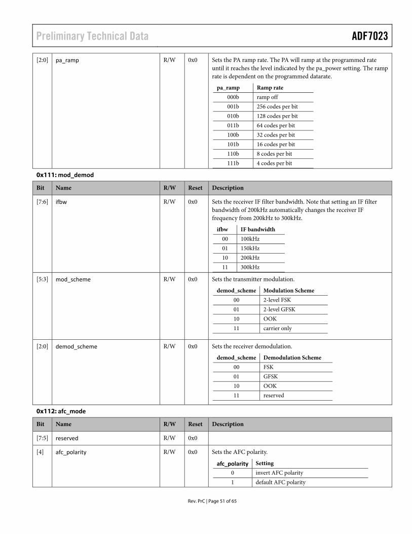
Preliminary Technical Data ADF7023
Rev. PrC | Page 51 of 65
[2:0] pa_ramp R/W 0x0 Sets the PA ramp rate. The PA will ramp at the programmed rate until it reaches the level indicated by the pa_power setting. The ramp rate is dependent on the programmed datarate.
pa_ramp Ramp rate 000b ramp off 001b 256 codes per bit 010b 128 codes per bit 011b 64 codes per bit 100b 32 codes per bit 101b 16 codes per bit 110b 8 codes per bit 111b 4 codes per bit
0x111: mod_demod
Bit Name R/W Reset Description
[7:6] ifbw R/W 0x0 Sets the receiver IF filter bandwidth. Note that setting an IF filter bandwidth of 200kHz automatically changes the receiver IF frequency from 200kHz to 300kHz.
ifbw IF bandwidth 00 100kHz 01 150kHz 10 200kHz 11 300kHz
[5:3] mod_scheme R/W 0x0 Sets the transmitter modulation.
demod_scheme Modulation Scheme 00 2-level FSK 01 2-level GFSK 10 OOK 11 carrier only
[2:0] demod_scheme R/W 0x0 Sets the receiver demodulation.
demod_scheme Demodulation Scheme 00 FSK 01 GFSK 10 OOK 11 reserved
0x112: afc_mode
Bit Name R/W Reset Description
[7:5] reserved R/W 0x0
[4] afc_polarity R/W 0x0 Sets the AFC polarity.
afc_polarity Setting 0 invert AFC polarity 1 default AFC polarity
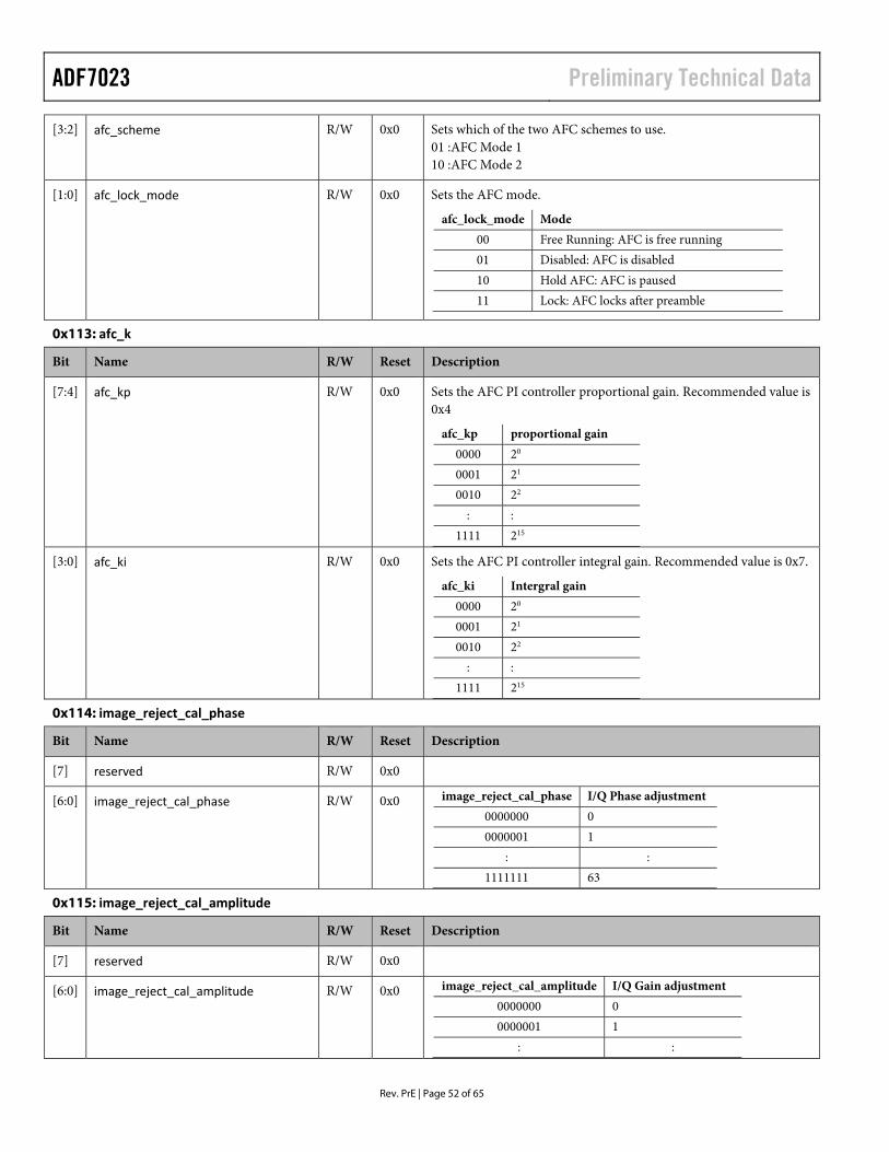
ADF7023 Preliminary Technical Data
Rev. PrE | Page 52 of 65
[3:2] afc_scheme R/W 0x0 Sets which of the two AFC schemes to use. 01 :AFC Mode 1 10 :AFC Mode 2
[1:0] afc_lock_mode R/W 0x0 Sets the AFC mode.
afc_lock_mode Mode 00 Free Running: AFC is free running 01 Disabled: AFC is disabled 10 Hold AFC: AFC is paused 11 Lock: AFC locks after preamble
0x113: afc_k
Bit Name R/W Reset Description
[7:4] afc_kp R/W 0x0 Sets the AFC PI controller proportional gain. Recommended value is 0x4
afc_kp proportional gain 0000 20
0001 21
0010 22
: : 1111 215
[3:0] afc_ki R/W 0x0 Sets the AFC PI controller integral gain. Recommended value is 0x7.
afc_ki Intergral gain 0000 20
0001 21
0010 22
: : 1111 215
0x114: image_reject_cal_phase
Bit Name R/W Reset Description
[7] reserved R/W 0x0
[6:0] image_reject_cal_phase R/W 0x0 image_reject_cal_phase I/Q Phase adjustment 0000000 0
0000001 1
: : 1111111 63
0x115: image_reject_cal_amplitude
Bit Name R/W Reset Description
[7] reserved R/W 0x0
[6:0] image_reject_cal_amplitude R/W 0x0 image_reject_cal_amplitude I/Q Gain adjustment 0000000 0
0000001 1
: :
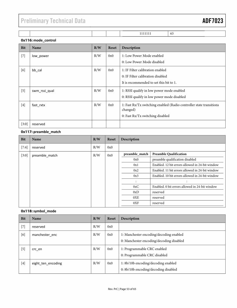
Preliminary Technical Data ADF7023
Rev. PrC | Page 53 of 65
1111111 63
0x116: mode_control
Bit Name R/W Reset Description
[7] low_power R/W 0x0 1: Low Power Mode enabled
0: Low Power Mode disabled
[6] bb_cal R/W 0x0 1: IF Filter calibration enabled
0: IF Filter calibration disabled
It is recommended to set this bit to 1.
[5] swm_rssi_qual R/W 0x0 1: RSSI qualify in low power mode enabled
0: RSSI qualify in low power mode disabled
[4] fast_rxtx R/W 0x0 1: Fast Rx/Tx switching enabled (Radio controller state transitions changed)
0: Fast Rx/Tx switching disabled
[3:0] reserved
0x117: preamble_match
Bit Name R/W Reset Description
[7:4] reserved R/W 0x0
[3:0] preamble_match R/W 0x0 preamble_match Preamble Qualification 0x0 preamble qualification disabled
0x1 Enabled. 12 bit errors allowed in 24-bit window
0x2 Enabled. 11 bit errors allowed in 24-bit window
0x3 Enabled. 10 bit errors allowed in 24-bit window
: : 0xC Enabled. 0 bit errors allowed in 24-bit window 0xD reserved 0XE reserved 0XF reserved
0x118: symbol_mode
Bit Name R/W Reset Description
[7] reserved R/W 0x0
[6] manchester_enc R/W 0x0 1: Manchester encoding/decoding enabled
0: Manchester encoding/decoding disabled
[5] crc_en R/W 0x0 1: Programmable CRC enabled
0: Programmable CRC disabled
[4] eight_ten_encoding R/W 0x0 1: 8b/10b encoding/decoding enabled
0: 8b/10b encoding/decoding disabled
ADF7023 Preliminary Technical Data
Rev. PrE | Page 54 of 65
[3] data_whitening R/W 0x0 1: Data whitening/de-whitening enabled
0: Data whitening/de-whitening disabled
[2:0] symbol_length R/W 0x0 symbol_length 000 8 bit (recommended except when 8b/10b is being
used)
001 10 bit (for 8b/10b encoding) 010 reserved
: : 111 reserved
0x119: preamble_len
Bit Name R/W Reset Description
[7:0] preamble_len R/W 0x0 Length of preamble in bytes. Example a value of decimal 3 results in a preamble of 24 bits.
0x11A: crc_poly_0
Bit Name R/W Reset Description
[7:0] crc_poly[7:0] R/W 0x0 Lower byte of crc_poly[15:0], which sets the CRC polynomial.
Refer to the Packet Format section on page 26.
0x11B: crc_poly_1
Bit Name R/W Reset Description
[7:0] crc_poly[15:8] R/W 0x0 Upper byte of crc_poly[15:0] which sets the CRC polynomial.
Refer to the Packet Format section on page 26.
0x11C: sync_control
Bit Name R/W Reset Description
[7:6] sync_error_tol R/W 0x0 Sets the sync word error tolerance in bits.
sync_error_tol Bit error tolerance 00 0 bit errors allowed
01 1 bit error allowed 10 2 bit error allowed 11 3 bit error allowed
[5] reserved R/W 0x0
[4:0] sync_word_length R/W 0x0 Sets the sync word length in bits. 24 bits is the maximum. Note that the sync word matching length can be any value up to 24 bits, but the transmitted sync word pattern is a multiple of 8 bits. Hence, for non-byte-length sync words, the transmitted sync pattern should be filled out with the preamble pattern.
sync_word_length Length in bits 00000 0
00001 1 : :
11000 24
Preliminary Technical Data ADF7023
Rev. PrC | Page 55 of 65
0x11D: sync_byte_0
Bit Name R/W Reset Description
[7:0] sync_byte[7:0] R/W 0x0 Lower byte of sync word pattern. The sync word pattern is transmitted most significant bit first starting with sync_byte[7:0].
If the sync word matching length is >16 bits then sync_byte_0, sync_byte_1 and sync_byte_2 are all transmitted for a total of 24 bits.
If the sync word length is between 8 and 15 then sync_byte_1 and sync_byte_2 are transmitted.
If the sync word length is between 1 and 7 then sync_byte_2 is transmitted for a total of 8 bits.
If the sync word length is 0 then no sync bytes are transmitted.
0x11E: sync_byte_1
Bit Name R/W Reset Description
[7:0] sync_byte[15:8] R/W 0x0 Mid byte of sync word pattern.
0x11F: sync_byte_2
Bit Name R/W Reset Description
[7:0] sync_byte[23:16] R/W 0x0 Upper byte of sync word pattern.
0x120: tx_base_adr
Bit Name R/W Reset Description
[7:0] tx_base_adr R/W 0x0 Address in Packet RAM of transmit packet. This address indicates to the comms processor the location of the first byte of the transmit packet
0x121: rx_base_adr
Bit Name R/W Reset Description
[7:0] rx_base_adr R/W 0x0 Address in Packet RAM of receive packet. The comms processor will write any qualified received packet to Packet RAM, starting at this memory location.
0x122: packet_length_control
Bit Name R/W Reset Description
[7] data_byte R/W 0x0 Over the air arrangement of each transmitted Packet RAM byte. Byte transmitted either MSB or LSB first. The same setting should be used on the Tx and Rx side of the link.
1: Data byte MSB first
0: Data byte LSB first
[6] packet_len R/W 0x0 1: Fixed packet length mode. Fixed packet length in tx and rx, given by packet_lenght_max.
0: Variable packet length mode. In rx mode packet length is given by first byte in Packet RAM. In tx mode the packet length is given by packet_lenght_max.
ADF7023 Preliminary Technical Data
Rev. PrE | Page 56 of 65
[5] crc_en R/W 0x0 1: Append CRC in transmit mode. Check CRC in receive mode.
0: No CRC addition in transmit mode. No CRC check in receive mode.
[4:3] reserved R/W 0x0
[2:0] length_offset R/W 0x0 Offset value in bytes that is added to the packet_length value so the communications processor knows the correct number of bytes to read. (does not include CRC). Useful in legacy systems where the definition of the packet length may or may not include CRC.
length_offset bytes 000 -4
001 -3 010 -2 011 -1 100 0 101 1 110 2 111 3
0x123: packet_length_max
Bit Name R/W Reset Description
[7:0] packet_length_max R/W 0x0 If variable packet length mode is used (packet_len_control = 0), then packet_length_max sets the maximum packet length in bytes.
If fixed packet length mode is used (packet_len_control = 1), then packet_length_max sets the length of the fixed packet in bytes.
Note that the packet length is defined as the number of bytes from the end of the sync word to the start of the CRC. It also does not include the length_offset value
0x124: reserved
Bit Name R/W Reset Description
[7:0] reserved R/W 0x0 Set to 0x0
0x125: address_match_offset
Bit Name R/W Reset Description
[7:0] address_match_offset R/W 0x0 Location of first byte of address information in Packet RAM
0x126: address_length
Bit Name R/W Reset Description
[7:0] address_length R/W 0x0 Number of bytes in each address field (NADR)
0x127 – 0x13F
Address Bit R/W Reset Description
0x127 [7:0] R/W 0x0 Address match byte 0
0x128 [7:0] R/W 0x0 Address mask byte 0
Preliminary Technical Data ADF7023
Rev. PrC | Page 57 of 65
0x129 [7:0] R/W 0x0 Address match byte 1
0x12A [7:0] R/W 0x0 Address mask byte 1
: :
[7:0] R/W 0x0 Address Match byte NADR-1
[7:0] R/W 0x0 Address Mask byte NADR-1
[7:0] R/W 0x0 0x00 to end or NADR for another address check sequence.
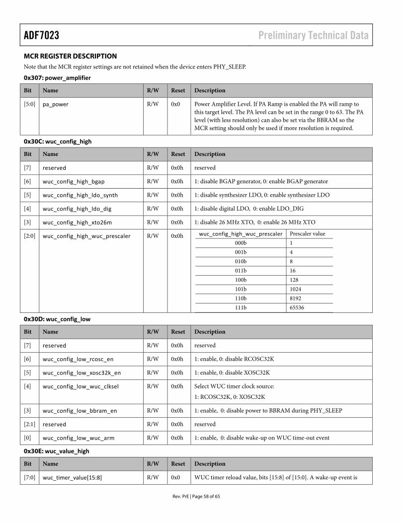
ADF7023 Preliminary Technical Data
Rev. PrE | Page 58 of 65
MCR REGISTER DESCRIPTION Note that the MCR register settings are not retained when the device enters PHY_SLEEP.
0x307: power_amplifier
Bit Name R/W Reset Description
[5:0] pa_power R/W 0x0 Power Amplifier Level. If PA Ramp is enabled the PA will ramp to this target level. The PA level can be set in the range 0 to 63. The PA level (with less resolution) can also be set via the BBRAM so the MCR setting should only be used if more resolution is required.
0x30C: wuc_config_high
Bit Name R/W Reset Description
[7] reserved R/W 0x0h reserved
[6] wuc_config_high_bgap R/W 0x0h 1: disable BGAP generator, 0: enable BGAP generator
[5] wuc_config_high_ldo_synth R/W 0x0h 1: disable synthesizer LDO, 0: enable synthesizer LDO
[4] wuc_config_high_ldo_dig R/W 0x0h 1: disable digital LDO, 0: enable LDO_DIG
[3] wuc_config_high_xto26m R/W 0x0h 1: disable 26 MHz XTO, 0: enable 26 MHz XTO
[2:0] wuc_config_high_wuc_prescaler R/W 0x0h wuc_config_high_wuc_prescaler Prescaler value 000b 1
001b 4 010b 8 011b 16 100b 128 101b 1024 110b 8192 111b 65536
0x30D: wuc_config_low
Bit Name R/W Reset Description
[7] reserved R/W 0x0h reserved
[6] wuc_config_low_rcosc_en R/W 0x0h 1: enable, 0: disable RCOSC32K
[5] wuc_config_low_xosc32k_en R/W 0x0h 1: enable, 0: disable XOSC32K
[4] wuc_config_low_wuc_clksel R/W 0x0h Select WUC timer clock source:
1: RCOSC32K, 0: XOSC32K
[3] wuc_config_low_bbram_en R/W 0x0h 1: enable, 0: disable power to BBRAM during PHY_SLEEP
[2:1] reserved R/W 0x0h reserved
[0] wuc_config_low_wuc_arm R/W 0x0h 1: enable, 0: disable wake-up on WUC time-out event
0x30E: wuc_value_high
Bit Name R/W Reset Description
[7:0] wuc_timer_value[15:8] R/W 0x0 WUC timer reload value, bits [15:8] of [15:0]. A wake-up event is
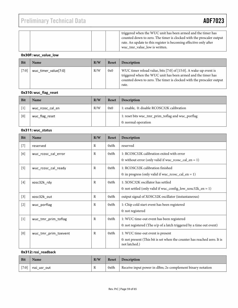
Preliminary Technical Data ADF7023
Rev. PrC | Page 59 of 65
triggered when the WUC unit has been armed and the timer has counted down to zero. The timer is clocked with the prescaler output rate. An update to this register is becoming effective only after wuc_tmr_value_low is written.
0x30F: wuc_value_low
Bit Name R/W Reset Description
[7:0] wuc_timer_value[7:0] R/W 0x0 WUC timer reload value, bits [7:0] of [15:0]. A wake-up event is triggered when the WUC unit has been armed and the timer has counted down to zero. The timer is clocked with the prescaler output rate.
0x310: wuc_flag_reset
Bit Name R/W Reset Description
[1] wuc_rcosc_cal_en R/W 0x0 1: enable, 0: disable RCOSC32K calibration
[0] wuc_flag_reset 1: reset bits wuc_tmr_prim_toflag and wuc_porflag
0: normal operation
0x311: wuc_status
Bit Name R/W Reset Description
[7] reserved R 0x0h reserved
[6] wuc_rcosc_cal_error R 0x0h 1: RCOSC32K calibration exited with error
0: without error (only valid if wuc_rcosc_cal_en = 1)
[5] wuc_rcosc_cal_ready R 0x0h 1: RCOSC32K calibration finished
0: in progress (only valid if wuc_rcosc_cal_en = 1)
[4] xosc32k_rdy R 0x0h 1: XOSC32K oscillator has settled
0: not settled (only valid if wuc_config_low_xosc32k_en = 1)
[3] xosc32k_out R 0x0h output signal of XOSC32K oscillator (instantaneous)
[2] wuc_porflag R 0x0h 1: Chip cold start event has been registered
0: not registered
[1] wuc_tmr_prim_toflag R 0x0h 1: WUC time-out event has been registered
0: not registered (The o/p of a latch triggered by a time out event)
[0] wuc_tmr_prim_toevent R 0x0h 1: WUC time-out event is present
0: not present (This bit is set when the counter has reached zero. It is not latched.)
0x312: rssi_readback
Bit Name R/W Reset Description
[7:0] rssi_usr_out R 0x0h Receive input power in dBm; 2s-complement binary notation
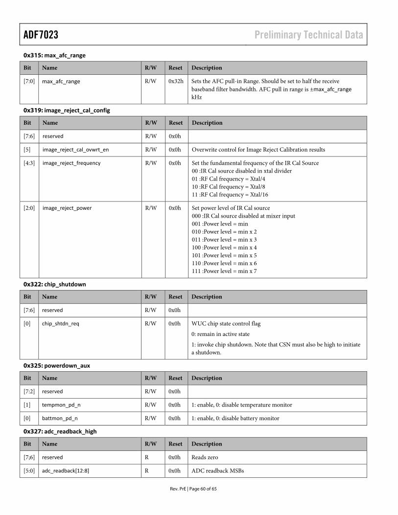
ADF7023 Preliminary Technical Data
Rev. PrE | Page 60 of 65
0x315: max_afc_range
Bit Name R/W Reset Description
[7:0] max_afc_range R/W 0x32h Sets the AFC pull-in Range. Should be set to half the receive baseband filter bandwidth. AFC pull in range is ±max_afc_range kHz
0x319: image_reject_cal_config
Bit Name R/W Reset Description
[7:6] reserved R/W 0x0h
[5] image_reject_cal_ovwrt_en R/W 0x0h Overwrite control for Image Reject Calibration results
[4:3] image_reject_frequency R/W 0x0h Set the fundamental frequency of the IR Cal Source 00 :IR Cal source disabled in xtal divider 01 :RF Cal frequency = Xtal/4 10 :RF Cal frequency = Xtal/8 11 :RF Cal frequency = Xtal/16
[2:0] image_reject_power R/W 0x0h Set power level of IR Cal source 000 :IR Cal source disabled at mixer input 001 :Power level = min 010 :Power level = min x 2 011 :Power level = min x 3 100 :Power level = min x 4 101 :Power level = min x 5 110 :Power level = min x 6 111 :Power level = min x 7
0x322: chip_shutdown
Bit Name R/W Reset Description
[7:6] reserved R/W 0x0h
[0] chip_shtdn_req R/W 0x0h WUC chip state control flag
0: remain in active state
1: invoke chip shutdown. Note that CSN must also be high to initiate a shutdown.
0x325: powerdown_aux
Bit Name R/W Reset Description
[7:2] reserved R/W 0x0h
[1] tempmon_pd_n R/W 0x0h 1: enable, 0: disable temperature monitor
[0] battmon_pd_n R/W 0x0h 1: enable, 0: disable battery monitor
0x327: adc_readback_high
Bit Name R/W Reset Description
[7;6] reserved R 0x0h Reads zero
[5:0] adc_readback[12:8] R 0x0h ADC readback MSBs
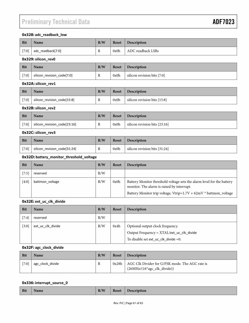
Preliminary Technical Data ADF7023
Rev. PrC | Page 61 of 65
0x328: adc_readback_low
Bit Name R/W Reset Description
[7:0] adc_readback[7:0] R 0x0h ADC readback LSBs
0x329: silicon_rev0
Bit Name R/W Reset Description
[7:0] silicon_revision_code[7:0] R 0x0h silicon revision bits [7:0]
0x32A: silicon_rev1
Bit Name R/W Reset Description
[7:0] silicon_revision_code[15:8] R 0x0h silicon revision bits [15:8]
0x32B: silicon_rev2
Bit Name R/W Reset Description
[7:0] silicon_revision_code[23:16] R 0x0h silicon revision bits [23:16]
0x32C: silicon_rev3
Bit Name R/W Reset Description
[7:0] silicon_revision_code[31:24] R 0x0h silicon revision bits [31:24]
0x32D: battery_monitor_threshold_voltage
Bit Name R/W Reset Description
[7:5] reserved R/W
[4:0] battmon_voltage R/W 0x0h Battery Monitor threshold voltage sets the alarm level for the battery monitor. The alarm is raised by interrupt.
Battery Monitor trip voltage, Vtrip=1.7V + 62mV * battmon_voltage
0x32E: ext_uc_clk_divide
Bit Name R/W Reset Description
[7:4] reserved R/W
[3:0] ext_uc_clk_divide R/W 0x4h Optional output clock frequency.
Output Frequency = XTAL/ext_uc_clk_divide
To disable set ext_uc_clk_divide =0.
0x32F: agc_clock_divide
Bit Name R/W Reset Description
[7:0] agc_clock_divide R 0x28h AGC Clk Divider for G/FSK mode. The AGC rate is (26MHz/(16*agc_clk_divide))
0x336: interrupt_source_0
Bit Name R/W Reset Description
ADF7023 Preliminary Technical Data
Rev. PrE | Page 62 of 65
[7] interrupt_num_wakeups R 0x0h Number of wakeups has reached threshold.
[6] interrupt_aes_done R 0x0h AES operation has completed
[5] interrupt_rssi_det R 0x0h RSSI above threshold detected (Low Power Rx Mode) interrupt
[4] interrupt_tx_eof R 0x0h Packet transmission finished interrupt
[3] interrupt_address_match_rx R 0x0h Address match interrupt
[2] interrupt_crc_correct_rx R 0x0h Correct CRC detect interrupt
[1] interrupt_sync_byte_detect R 0x0h Sync word detect interrupt
[0] interrupt_premable_detect R 0x0h Preamble detect interrupt
0x337: interrupt_source_1
Bit Name R/W Reset Description
[7] battery_alarm R 0x0h Battery voltage has dropped below user set threshold
[6] rc_ready R 0x0h Radio controller command finished. Ready to accept a new command.
[5] unused R 0x0h
[4] wuc_timeout R 0x0h Wake up Timer has timed out
[3] unused R 0x0h
[2] unused R 0x0h
[1] spi_ready R 0x0h SPI ready for access
[0] rc_error R 0x0h Radio Controller error
0x338: calibration_control
Bit Name R/W Reset Description
[7:2] reserved R/W 0x0h
[1] synth_cal_en R/W 0x0h 1: Enables 0: Disables the synthesizer calibration state machine.
[0] rxbb_cal_en R/W 0x0h 1: Enable, 0: disable RXBB calibration
0x339: calibration_status
Bit Name R/W Reset Description
[7:3] reserved R/W 0x0h
[2] pa_ramp_finished R/W 0x0h
[1] synth_cal_ready R/W 0x0h 1: Synthesizer calibration finished successfully. 0: Synthesizer calibration in progress
[0] rxbb_cal_ready R/W 0x0h Receive IF Filter calibration, 1: complete; 0: in progress (valid while rxbb_cal_en = 1)
0x359: adc_config_low
Bit Name R/W Reset Description
Preliminary Technical Data ADF7023
Rev. PrC | Page 63 of 65
[7:6] adc_acquisition R/W 0x0h 00=4; 01=6; 10=10; 11=18 clock cycles for acquisition
[5:4] adc_resol R/W 0x0h 00=12bit; 01=10bit; 10=13bit; 11=13bit
[3:2] adc_ref_chsel R/W 0x1h 00=RSSI; 01=External AIN; 10=Temp Sensor; 11 Unused
[1:0] adc_reference_control R/W 0x1h 00=1.85V; 01=1.95V; 10=1.75V; 11=1.65V Reference
0x35A: adc_config_high
Bit Name R/W Reset Description
[7] reserved R/W 0x0h
[6:5] filtered_adc_mode R/W 0x0h Filtering Mode 00: normal operation (no filter) 01: unfiltered AGC loop, filtered readback (update on MCR read - either by SPI or packet_handler). 10: unfiltered AGC loop, filtered readback (update at AGC clock rate)11: filtered AGC loop, filtered readback (update at the OOK rate ~1M/s)
[4] adc_ext_ref_enb R/W 0x1h Bring low to power down ADC Reference. Put into ADC_CLOCK_FREQ_DIVIDE register
[3:0] adc_analog_clk_divide R/W 0x1h ADC clock frequency divider)
0x35B: agc_ook_config
Bit Name R/W Reset Description
[7:6] reserved R/W 0x0h
[5:3] ook_agc_clk_ww R/W 0x2h AGC update rate during tracking phase:
AGC update = Fman / [2^(ook_agc_iad_ww+1)]
Where:
Fman = The Manchester symbol Rate.
Manchester encoding is recommended for OOK Note: ook_agc_iad_ww must be > = ook_agc_clk_ww
[2:0] ook_agc_iad_ww R/W 0x2h AGC update rate during acquisition phase:
AGC update = Fman / [(2^(ook_agc_clk_ww+1)]
Where:
Fman = The Manchester symbol Rate.
Manchester encoding is recommended for OOK. Note: ook_agc_iad_ww must be > = ook_agc_clk_ww
0x372: frequency_error_readback
Bit Name R/W Reset Description
[7:0] frequency_error_readback R 0x0h Frequency Error between received signal frequency and receive channel frequency = frequency_error_readback ×100Hz

ADF7023 Preliminary Technical Data
Rev. PrE | Page 64 of 65
0x3D2: xosc_config
Bit Name R/W Reset Description
[7:6] reserved R/W 0x0h write 0
[5:3] xosc_cap_dac R/W 0x0h 26MHz crystal oscillator (XOSC26M ) tuning capacitor control word
[2:0] reserved R/W 0x0h write 0
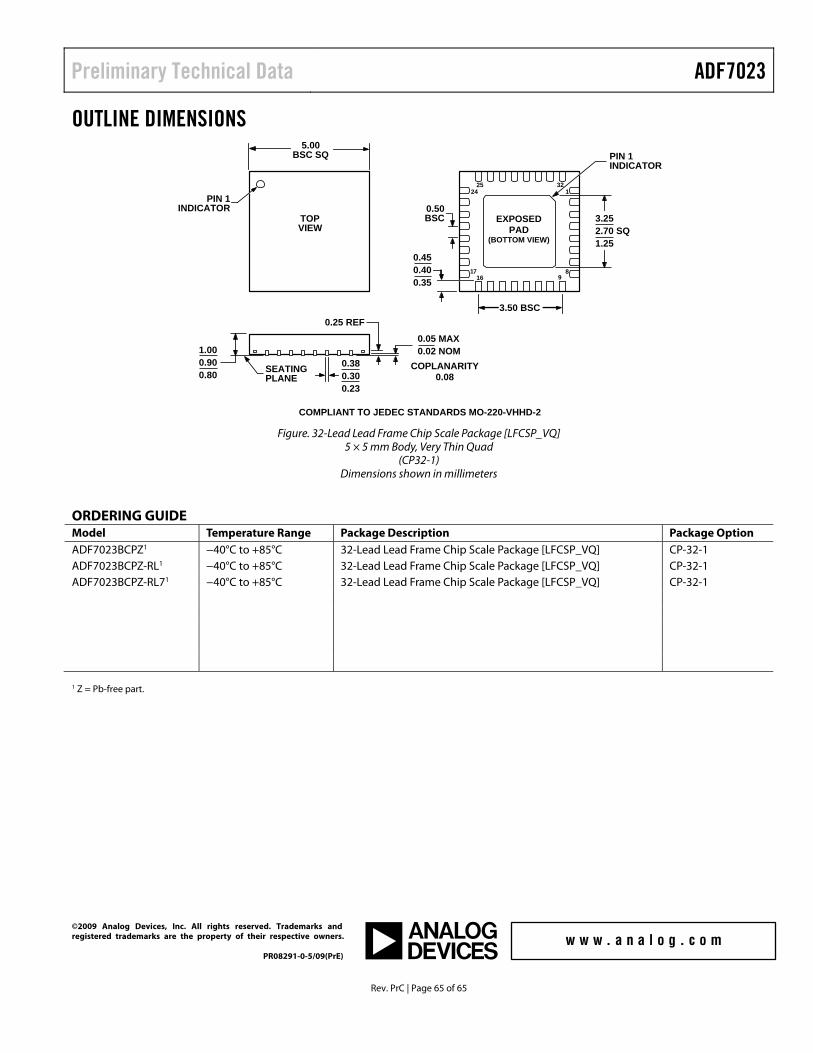
Preliminary Technical Data ADF7023
Rev. PrC | Page 65 of 65
OUTLINE DIMENSIONS
Figure. 32-Lead Lead Frame Chip Scale Package [LFCSP_VQ] 5 × 5 mm Body, Very Thin Quad
(CP32-1) Dimensions shown in millimeters
ORDERING GUIDE Model Temperature Range Package Description Package Option ADF7023BCPZ1 −40°C to +85°C 32-Lead Lead Frame Chip Scale Package [LFCSP_VQ] CP-32-1 ADF7023BCPZ-RL1 −40°C to +85°C 32-Lead Lead Frame Chip Scale Package [LFCSP_VQ] CP-32-1 ADF7023BCPZ-RL71 −40°C to +85°C 32-Lead Lead Frame Chip Scale Package [LFCSP_VQ] CP-32-1 1 Z = Pb-free part.
COMPLIANT TO JEDEC STANDARDS MO-220-VHHD-2
0.380.300.23
0.05 MAX0.02 NOM1.00
0.900.80 SEATING
PLANECOPLANARITY
0.08
132
89
2524
1617
0.450.400.35
3.50 BSC
0.50BSC
PIN 1INDICATOR
TOPVIEW
5.00BSC SQ
3.252.70 SQ1.25
PIN 1INDICATOR
EXPOSEDPAD
(BOTTOM VIEW)
0.25 REF
©2009 Analog Devices, Inc. All rights reserved. Trademarks and registered trademarks are the property of their respective owners. PR08291-0-5/09(PrE)