Embed Size (px)
Citation preview
1
Addressing Link-Level Design Tradeoffs for Integrated Photonic Interconnects
Michael Georgas, Jonathan Leu, Benjamin Moss, Chen Sun and Vladimir Stojanović
Massachusetts Institute of Technology
CICC 2011
2
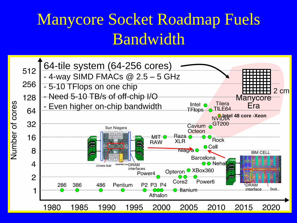
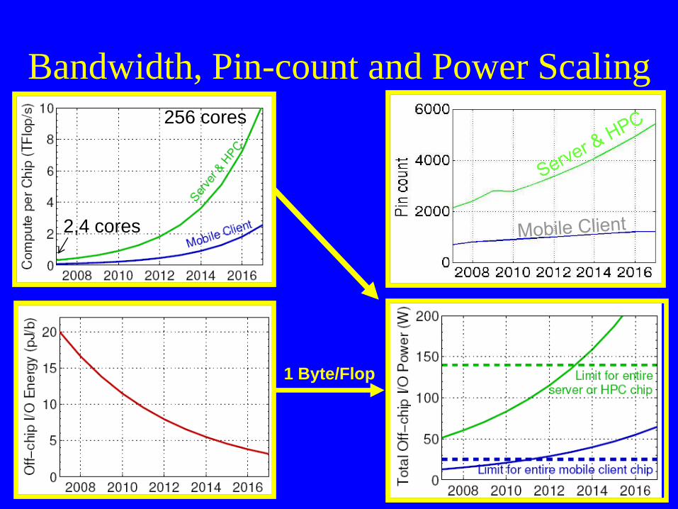
Manycore Socket Roadmap Fuels
Bandwidth
64-tile system (64-256 cores) - 4-way SIMD FMACs @ 2.5 – 5 GHz
- 5-10 TFlops on one chip
- Need 5-10 TB/s of off-chip I/O
- Even higher on-chip bandwidth
2 cm
Intel 48 core -Xeon
3
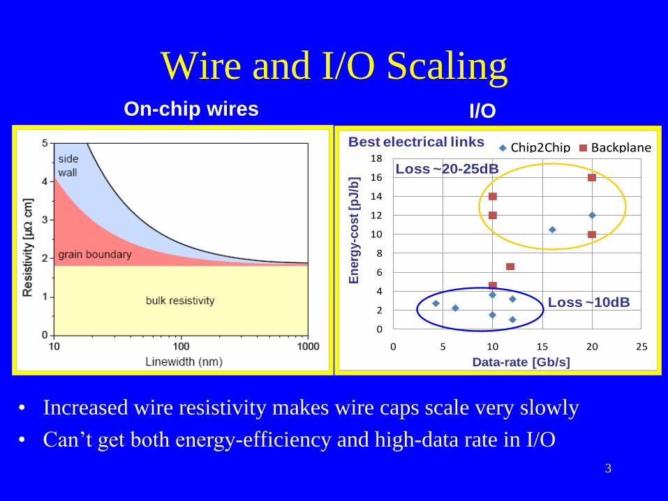
Wire and I/O Scaling On-chip wires
0
2
4
6
8
10
12
14
16
18
0 5 10 15 20 25
Chip2Chip Backplane
En
erg
y-c
ost
[pJ/b
]Data-rate [Gb/s]
Best electrical links
Loss ~10dB
Loss ~20-25dB
I/O
• Increased wire resistivity makes wire caps scale very slowly
• Can’t get both energy-efficiency and high-data rate in I/O
4
Bandwidth, Pin-count and Power Scaling
1 Byte/Flop
256 cores
2,4 cores
5
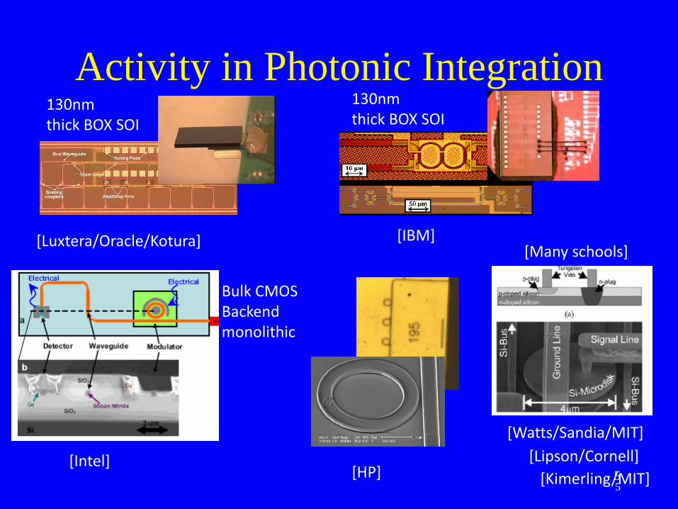
Activity in Photonic Integration
[Luxtera/Oracle/Kotura]
130nm thick BOX SOI
[IBM]
[HP]
[Watts/Sandia/MIT]
130nm thick BOX SOI
[Lipson/Cornell]
[Kimerling/MIT]
[Many schools]
5
[Intel]
Bulk CMOS Backend monolithic
6
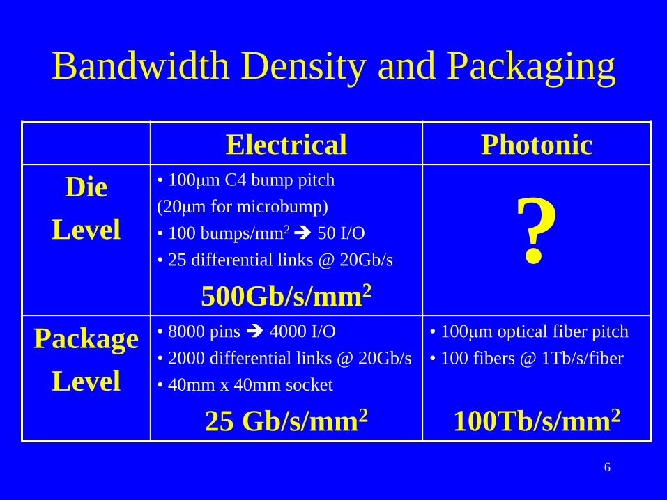
Bandwidth Density and Packaging
Electrical Photonic
Die
Level
• 100μm C4 bump pitch
(20μm for microbump)
• 100 bumps/mm2 50 I/O
• 25 differential links @ 20Gb/s
500Gb/s/mm2
? Package
Level
• 8000 pins 4000 I/O
• 2000 differential links @ 20Gb/s
• 40mm x 40mm socket
25 Gb/s/mm2
• 100μm optical fiber pitch
• 100 fibers @ 1Tb/s/fiber
100Tb/s/mm2
7
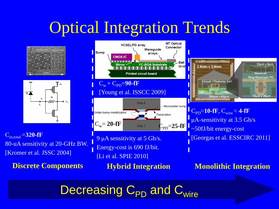
Optical Integration Trends
Discrete Components Hybrid Integration Monolithic Integration
Decreasing CPD and Cwire
CPD=25-fF
9 μA sensitivity at 5 Gb/s.
Energy-cost is 690 fJ/bit.
[Li et al. SPIE 2010]
Cw + CPD=90-fF
[Young et al. ISSCC 2009]
Cin,total =320-fF
80-uA sensitivity at 20-GHz BW.
[Kromer et al. JSSC 2004]
CPD≈10-fF, Cwire ≈ 4-fF
μA-sensitivity at 3.5 Gb/s
~50fJ/bit energy-cost
[Georgas et al. ESSCIRC 2011]
Cw= 20-fF
8
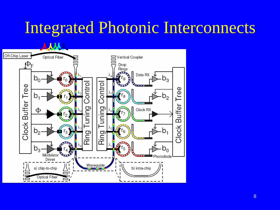
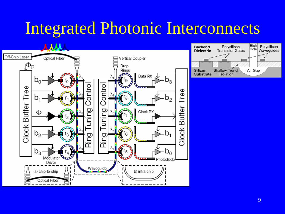
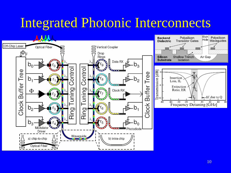
Integrated Photonic Interconnects
9
Integrated Photonic Interconnects
10
Integrated Photonic Interconnects
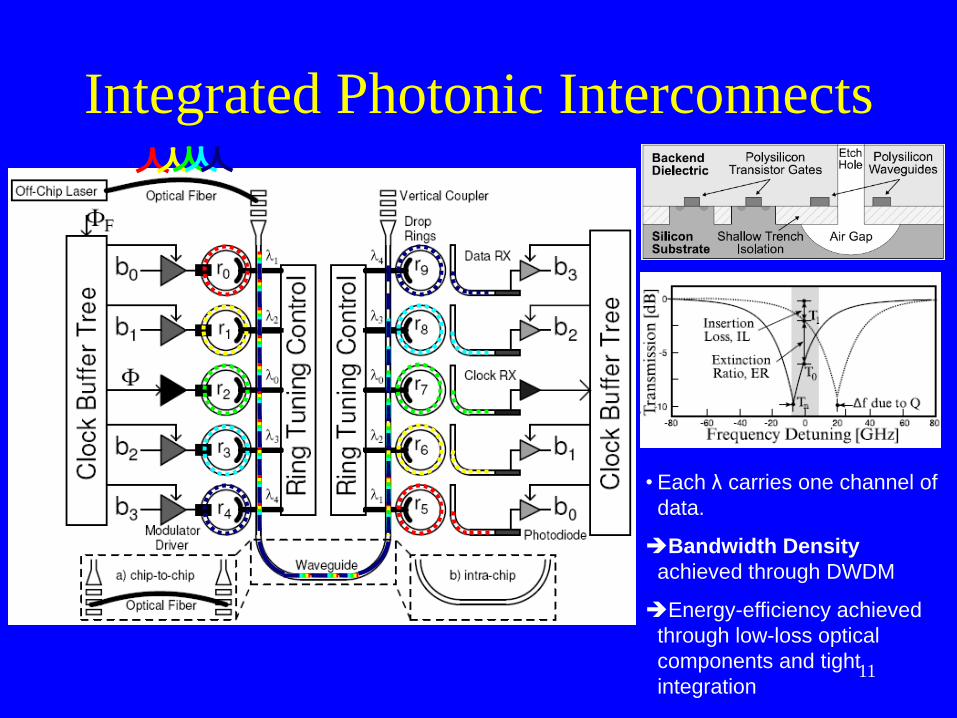
11
Integrated Photonic Interconnects
• Each λ carries one channel of
data.
Bandwidth Density
achieved through DWDM
Energy-efficiency achieved
through low-loss optical
components and tight
integration
12
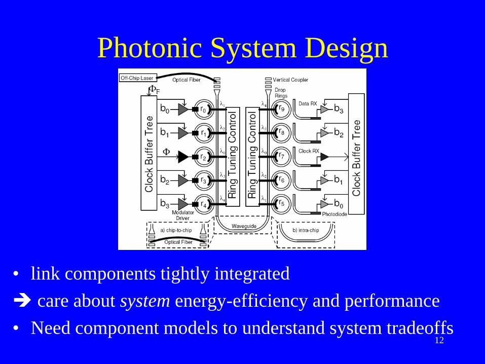
Photonic System Design
• link components tightly integrated
care about system energy-efficiency and performance
• Need component models to understand system tradeoffs
13
Outline
• Motivation
• Photonic Link Components
– Modulator and driver
– Receiver
– Single Link Analysis
• Towards a WDM Photonic Link
– Clock distribution
– Ring Tuning
– WDM Link Analysis
• Conclusion
14
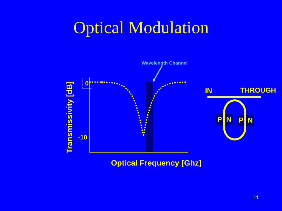
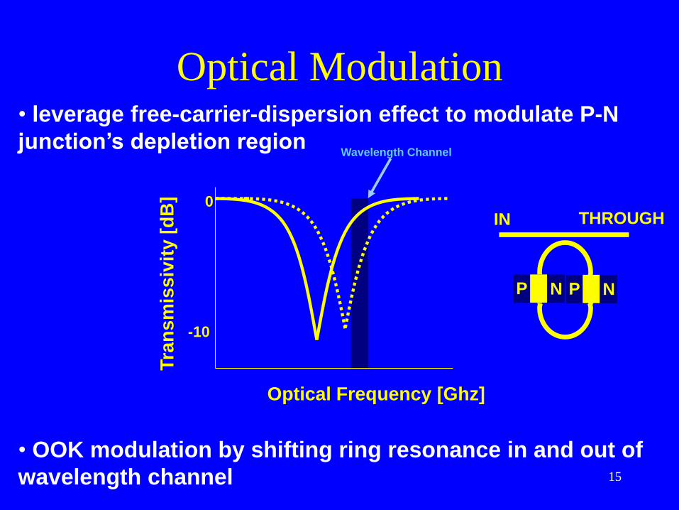
Optical Modulation
Optical Frequency [Ghz]
Tra
nsm
issiv
ity [
dB
] 0
-10
Wavelength Channel
IN THROUGH
P N P N
15
Optical Modulation
• OOK modulation by shifting ring resonance in and out of
wavelength channel
Optical Frequency [Ghz]
Tra
nsm
issiv
ity [
dB
] 0
-10
Wavelength Channel
• leverage free-carrier-dispersion effect to modulate P-N
junction’s depletion region
IN THROUGH
P N P N
16
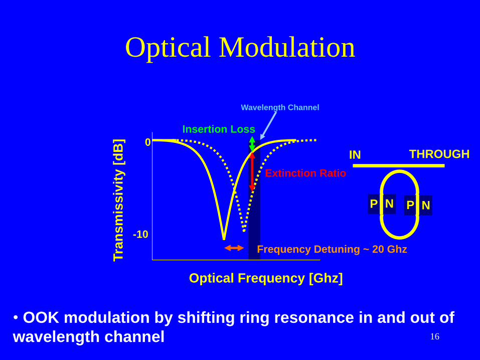
Optical Modulation
Optical Frequency [Ghz]
Tra
nsm
issiv
ity [
dB
] 0
-10
Wavelength Channel
Extinction Ratio
Insertion Loss
Frequency Detuning ~ 20 Ghz
IN THROUGH
P N P N
• OOK modulation by shifting ring resonance in and out of
wavelength channel
17
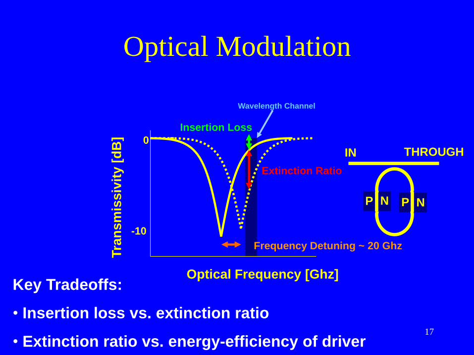
Optical Modulation
Key Tradeoffs:
• Insertion loss vs. extinction ratio
• Extinction ratio vs. energy-efficiency of driver
Optical Frequency [Ghz]
Tra
nsm
issiv
ity [
dB
] 0
-10
Wavelength Channel
Extinction Ratio
Insertion Loss
Frequency Detuning ~ 20 Ghz
IN THROUGH
P N P N
18
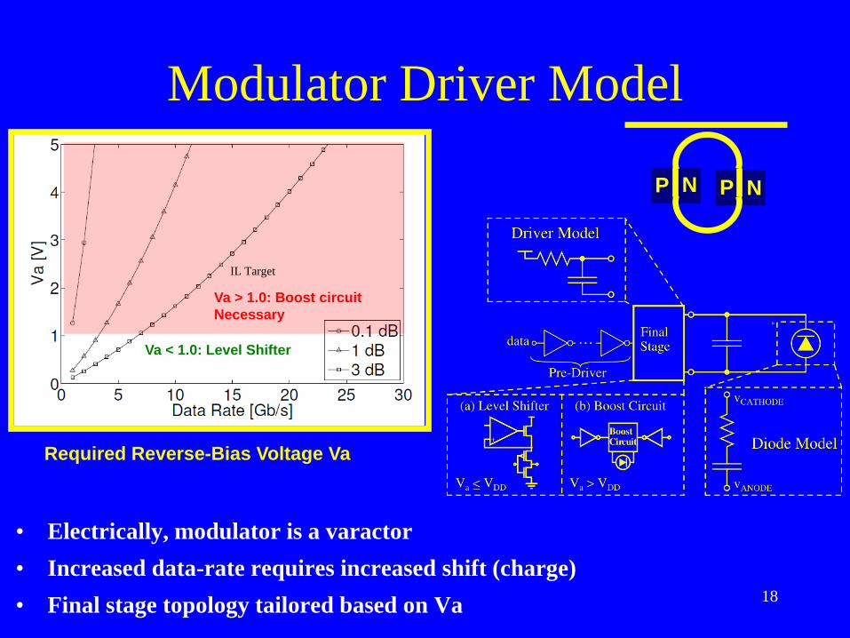
Modulator Driver Model
• Electrically, modulator is a varactor
• Increased data-rate requires increased shift (charge)
• Final stage topology tailored based on Va
Required Reverse-Bias Voltage Va
Va > 1.0: Boost circuit
Necessary
Va < 1.0: Level Shifter
IL Target
P N P N
19
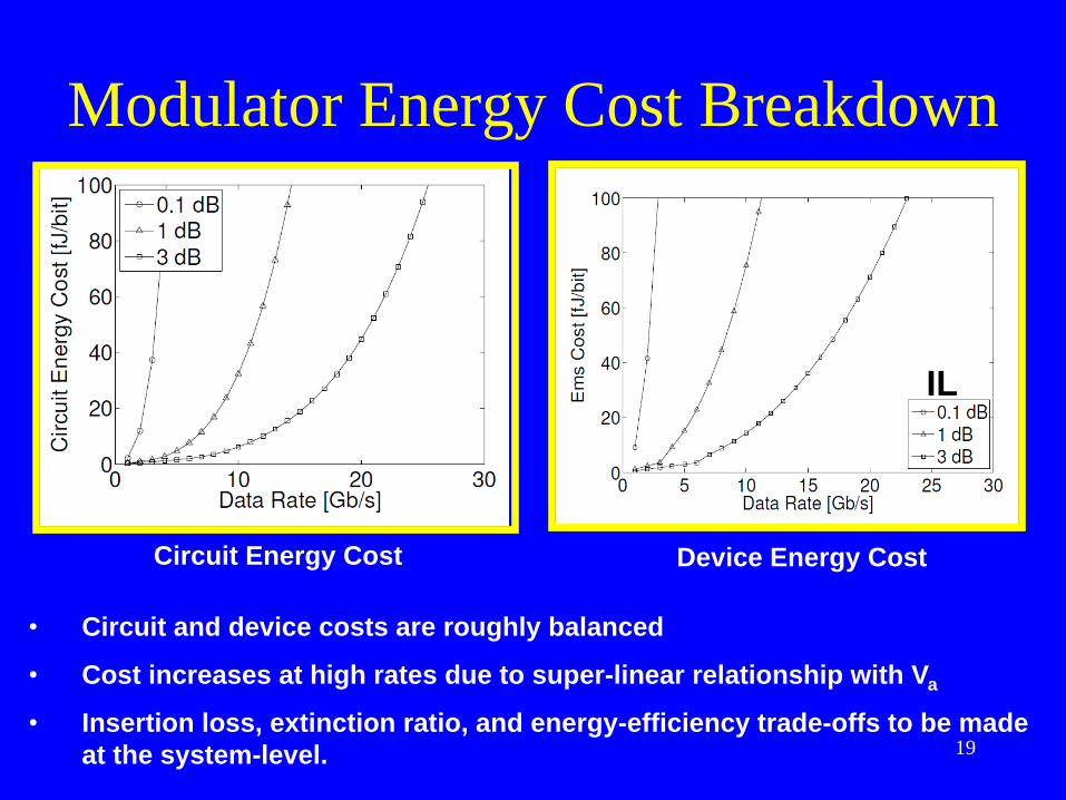
Modulator Energy Cost Breakdown
Circuit Energy Cost Device Energy Cost
• Circuit and device costs are roughly balanced
• Cost increases at high rates due to super-linear relationship with Va
• Insertion loss, extinction ratio, and energy-efficiency trade-offs to be made
at the system-level.
IL
20
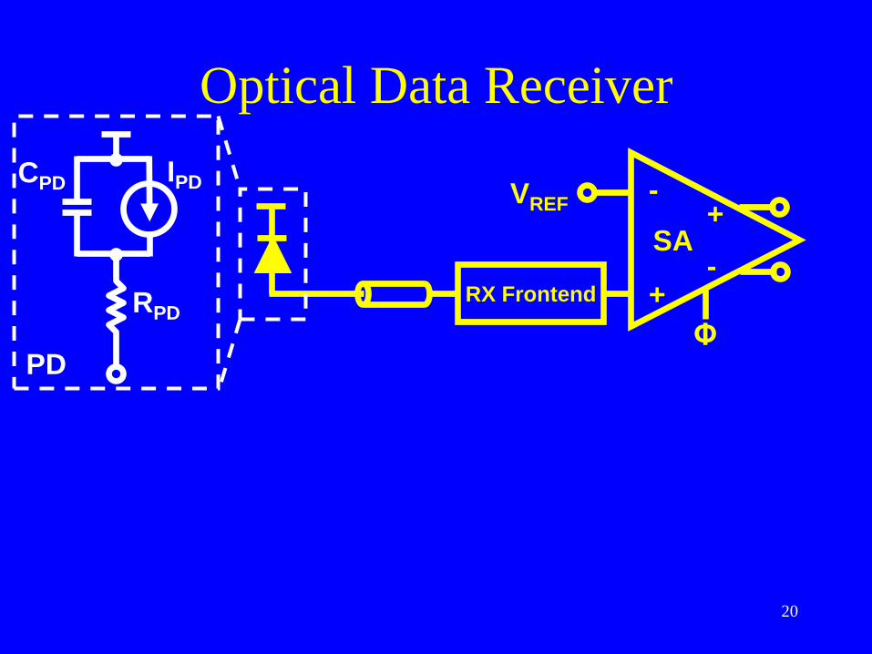
Optical Data Receiver
SA
-
+
+
-
VREF IPD CPD
RPD
PD
RX Frontend
Φ
21
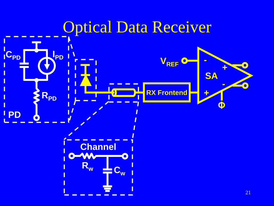
Optical Data Receiver
SA
-
+
+
-
VREF IPD CPD
RPD
PD
RX Frontend
Cw Rw
Channel
Φ
22
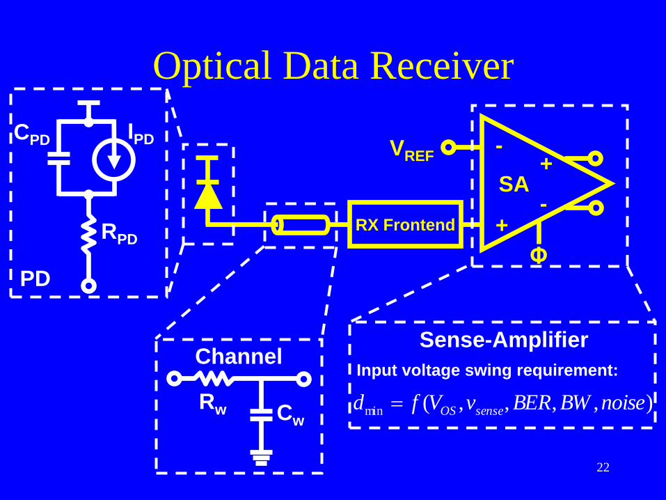
Optical Data Receiver
SA
-
+
+
-
VREF IPD CPD
RPD
PD
Cw Rw
Channel
RX Frontend
Sense-Amplifier
Input voltage swing requirement:
),,,,(min noiseBWBERvVfd senseOS
Φ
23
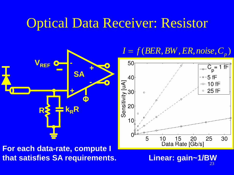
Optical Data Receiver: Resistor
R
For each data-rate, compute I
that satisfies SA requirements.
kRR
),,,,( pCnoiseERBWBERfI
SA
-
+
+
-
VREF
Linear: gain~1/BW
Φ
24
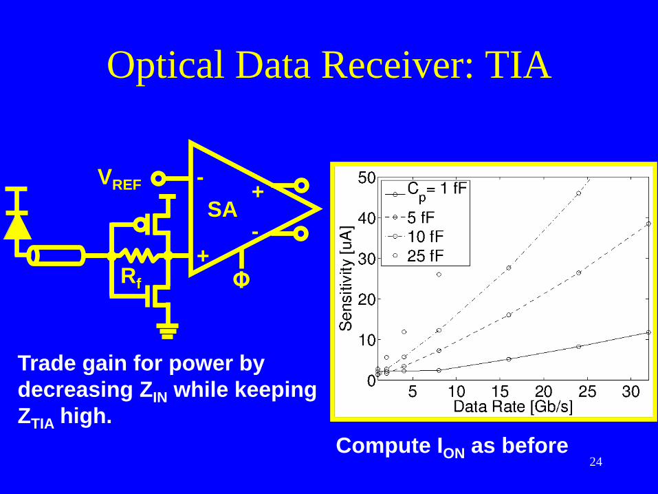
Optical Data Receiver: TIA
Compute ION as before
Rf
SA
-
+
+
-
VREF
Trade gain for power by
decreasing ZIN while keeping
ZTIA high.
Φ
25
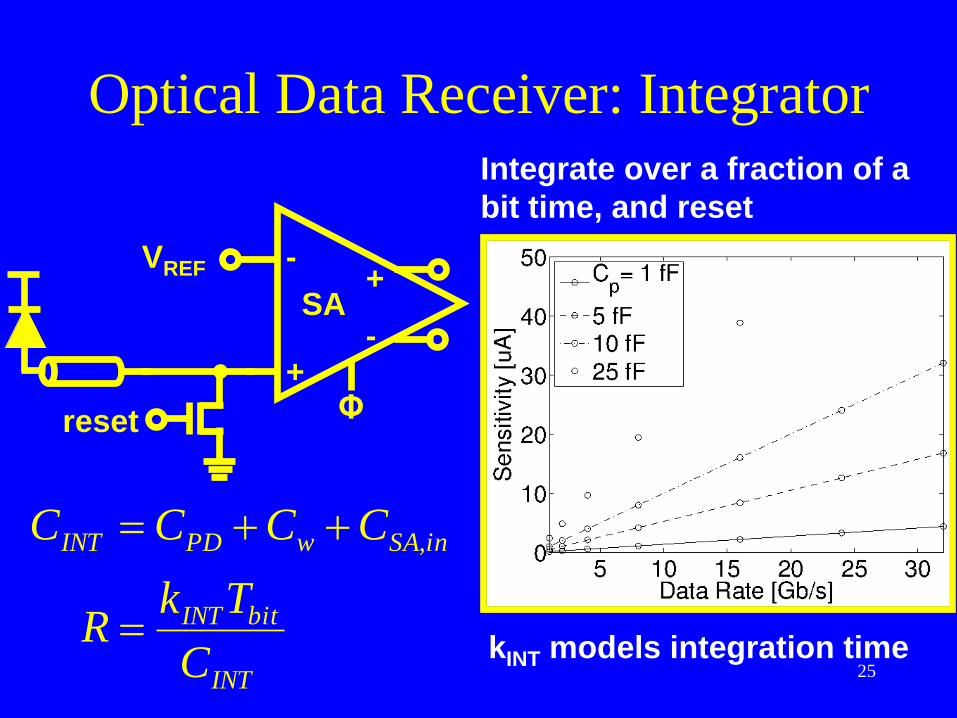
Optical Data Receiver: Integrator
reset
INT
bitINT
inSAwPDINT
C
TkR
CCCC
,
Integrate over a fraction of a
bit time, and reset
SA
-
+
+
-
VREF
kINT models integration time
Φ
26
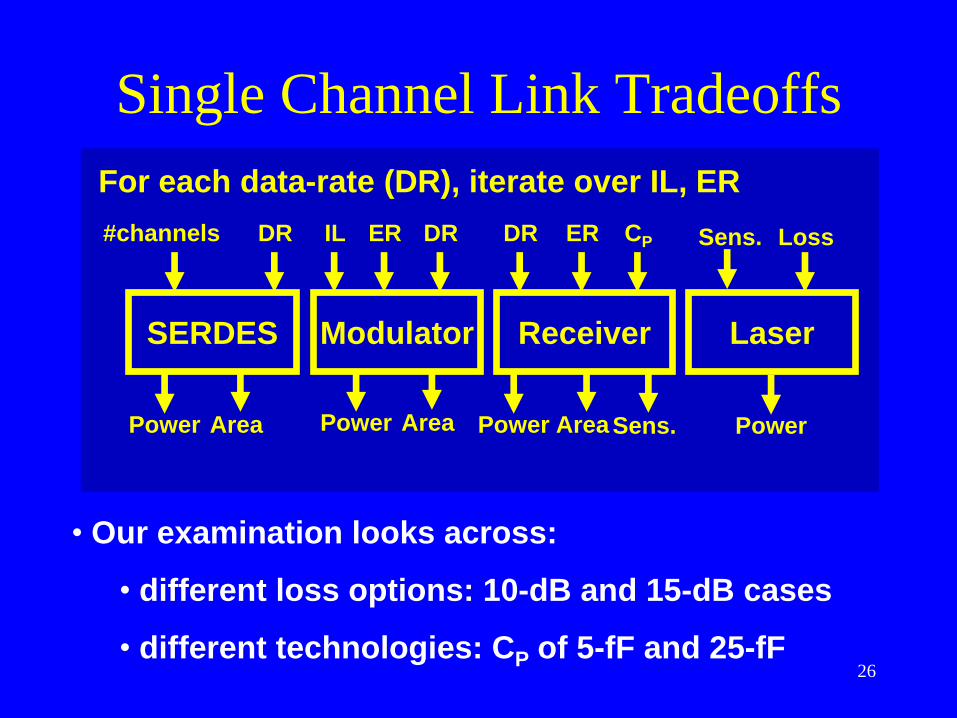
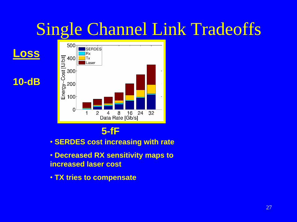
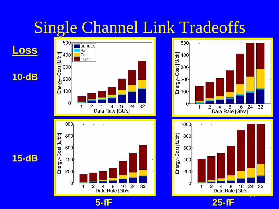
Single Channel Link Tradeoffs
• Our examination looks across:
• different loss options: 10-dB and 15-dB cases
• different technologies: CP of 5-fF and 25-fF
Modulator Receiver SERDES Laser
Power Area
DR #channels IL ER
Power Area Power Area Sens.
Sens.
Power
DR ER DR Loss
For each data-rate (DR), iterate over IL, ER
CP
27
Single Channel Link Tradeoffs
10-dB
Loss
5-fF • SERDES cost increasing with rate
• Decreased RX sensitivity maps to
increased laser cost
• TX tries to compensate
28
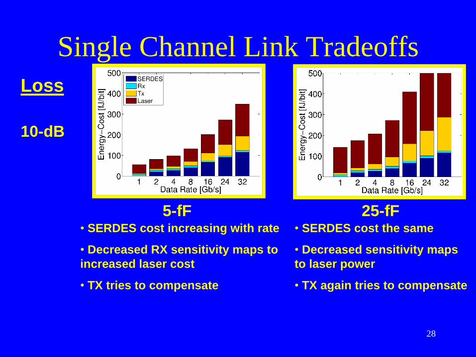
Single Channel Link Tradeoffs
10-dB
Loss
5-fF • SERDES cost increasing with rate
• Decreased RX sensitivity maps to
increased laser cost
• TX tries to compensate
25-fF • SERDES cost the same
• Decreased sensitivity maps
to laser power
• TX again tries to compensate
29
Single Channel Link Tradeoffs
10-dB
15-dB
Loss
5-fF 25-fF
30
Outline
• Motivation
• Photonic Link Components
– Modulator and driver
– Receiver
– Single Link Analysis
• Towards a WDM Photonic Link
– Clock distribution
– Ring Tuning
– WDM Link Analysis
• Conclusion
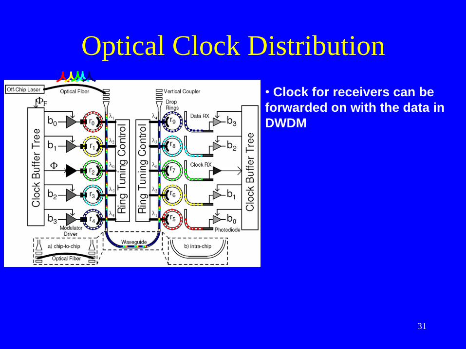
31
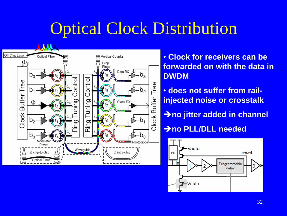
Optical Clock Distribution
• Clock for receivers can be
forwarded on with the data in
DWDM
32
Optical Clock Distribution
• Clock for receivers can be
forwarded on with the data in
DWDM
• does not suffer from rail-
injected noise or crosstalk
no jitter added in channel
no PLL/DLL needed
33
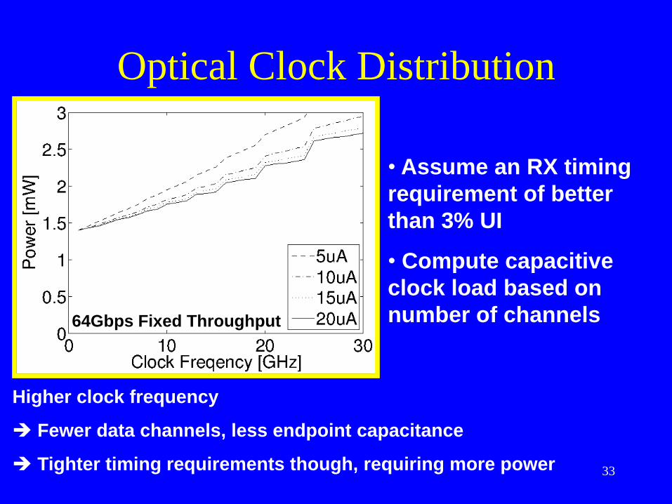
Optical Clock Distribution
• Assume an RX timing
requirement of better
than 3% UI
• Compute capacitive
clock load based on
number of channels
Higher clock frequency
Fewer data channels, less endpoint capacitance
Tighter timing requirements though, requiring more power
64Gbps Fixed Throughput
34 228 230 232 234 236
0.5
1
Frequency [THz]
Resp
onse
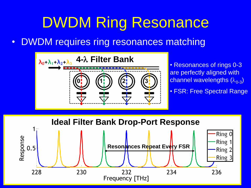
DWDM Ring Resonance
Resonances Repeat Every FSR
• Resonances of rings 0-3
are perfectly aligned with
channel wavelengths (0-3)
• FSR: Free Spectral Range
4- Filter Bank
Ideal Filter Bank Drop-Port Response
• DWDM requires ring resonances matching
35
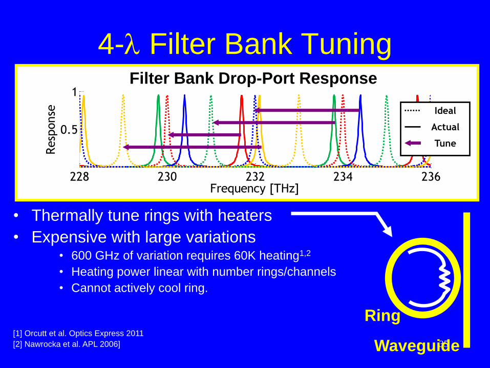
4- Filter Bank Tuning
228 230 232 234 236
0.5
1
Frequency [THz]
Resp
onse
Filter Bank Drop-Port Response
• Thermally tune rings with heaters
• Expensive with large variations • 600 GHz of variation requires 60K heating1,2
• Heating power linear with number rings/channels
• Cannot actively cool ring.
[1] Orcutt et al. Optics Express 2011
[2] Nawrocka et al. APL 2006]
Ideal
Actual
Tune
Ring
Waveguide
36
Nearest-Channel Tuning
228 230 232 234 236
0.5
1
Frequency [THz]
Resp
onse
Filter Bank Drop-Port Response
• Allow rings to just tune to the nearest channel – Reduces tuning range, saves heating power
– Electrically reshuffle bit positions as opposed to assigning a permanent fixed wavelength per ring
• Build an n-to-n electrical crossbar (grows with n2) – can we do better?
Ideal
Actual
Tune
37
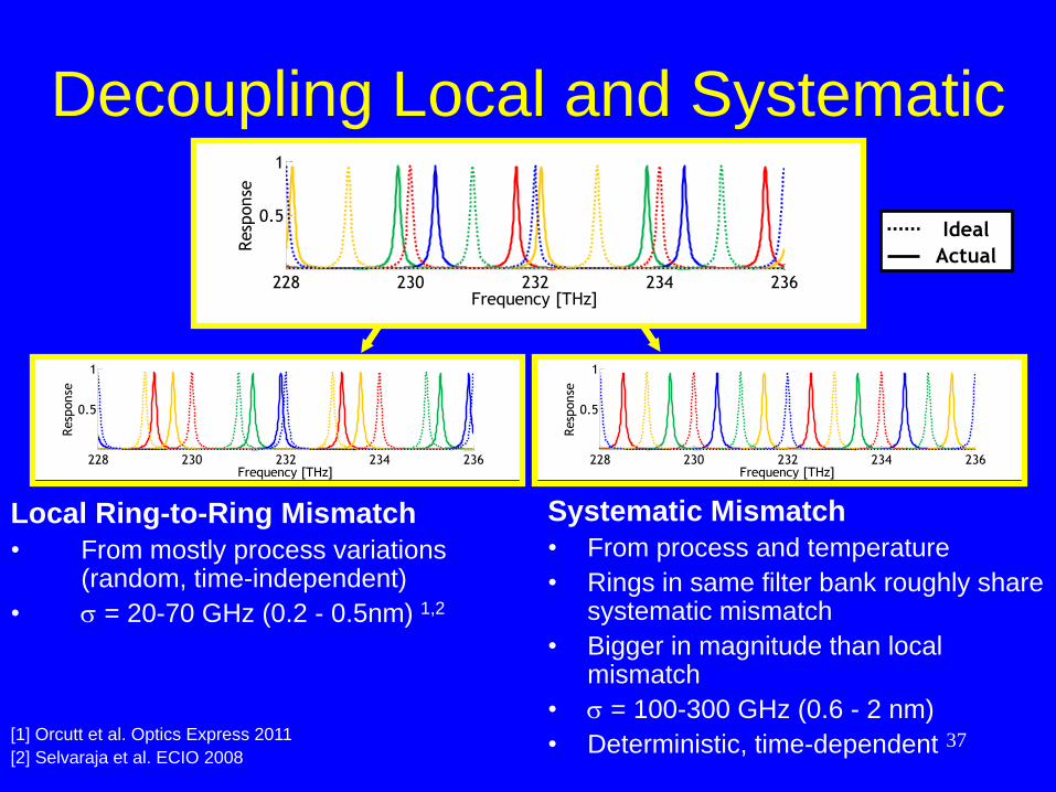
Decoupling Local and Systematic
228 230 232 234 236
0.5
1
Frequency [THz]
Resp
onse
Ideal
Actual
228 230 232 234 236
0.5
1
Frequency [THz]
Resp
onse
228 230 232 234 236
0.5
1
Frequency [THz]
Resp
onse
Local Ring-to-Ring Mismatch
• From mostly process variations (random, time-independent)
• = 20-70 GHz (0.2 - 0.5nm) 1,2
[1] Orcutt et al. Optics Express 2011
[2] Selvaraja et al. ECIO 2008
Systematic Mismatch
• From process and temperature
• Rings in same filter bank roughly share systematic mismatch
• Bigger in magnitude than local mismatch
• = 100-300 GHz (0.6 - 2 nm)
• Deterministic, time-dependent
38
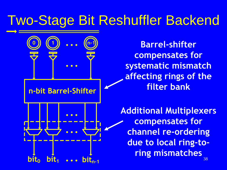
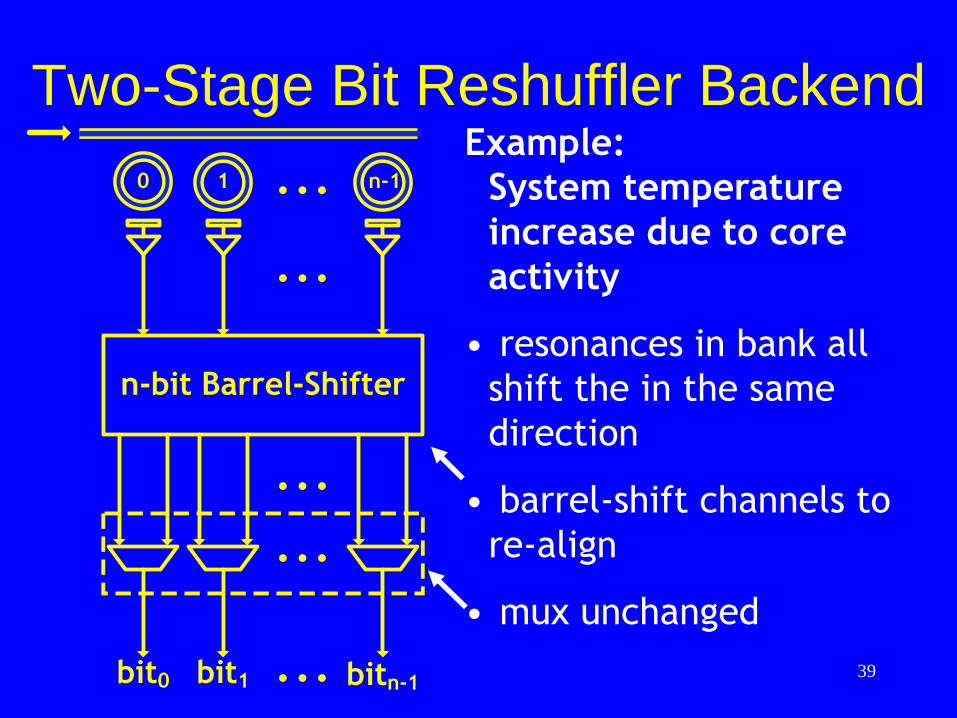
Two-Stage Bit Reshuffler Backend
Barrel-shifter
compensates for
systematic mismatch
affecting rings of the
filter bank
Additional Multiplexers
compensates for
channel re-ordering
due to local ring-to-
ring mismatches
n-bit Barrel-Shifter
0 1 n-1...
bit0
...
...
...
...
bit1 bitn-1
39
Two-Stage Bit Reshuffler Backend Example:
System temperature
increase due to core
activity
• resonances in bank all
shift the in the same
direction
• barrel-shift channels to
re-align
• mux unchanged
n-bit Barrel-Shifter
0 1 n-1...
bit0
...
...
...
...
bit1 bitn-1
40
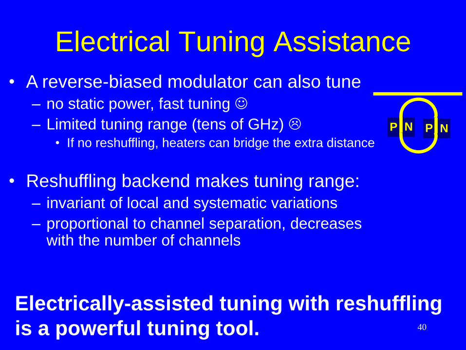
Electrical Tuning Assistance
• A reverse-biased modulator can also tune – no static power, fast tuning
– Limited tuning range (tens of GHz) • If no reshuffling, heaters can bridge the extra distance
• Reshuffling backend makes tuning range: – invariant of local and systematic variations
– proportional to channel separation, decreases with the number of channels
Electrically-assisted tuning with reshuffling
is a powerful tuning tool.
P N P N
41
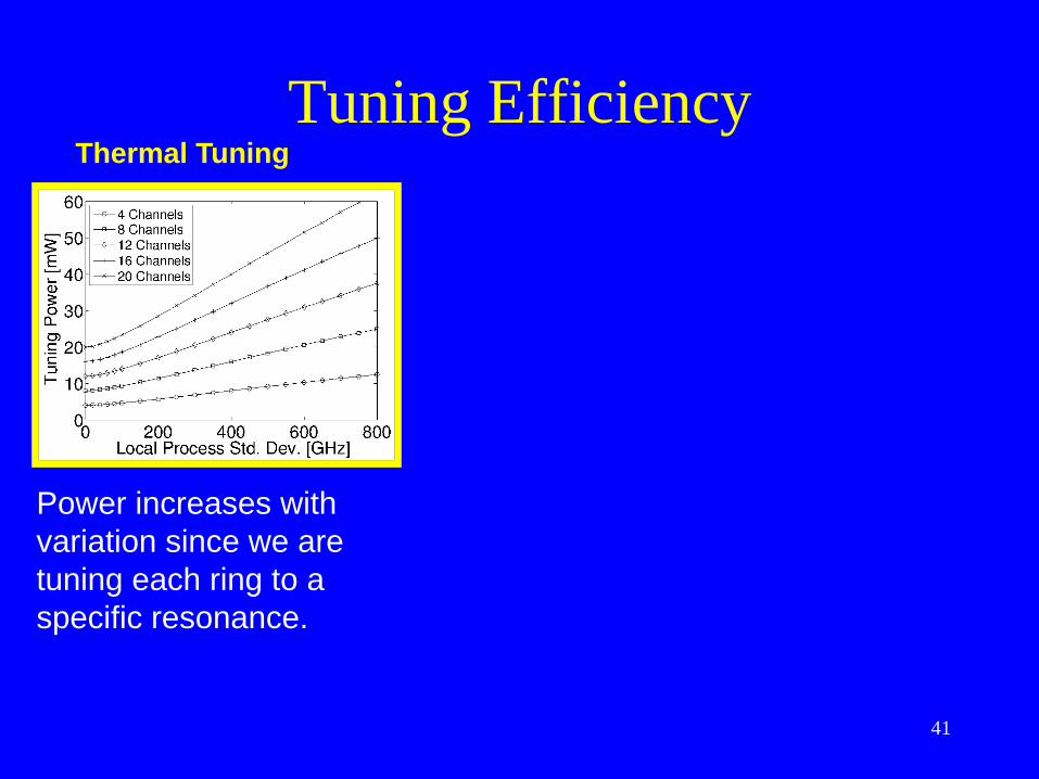
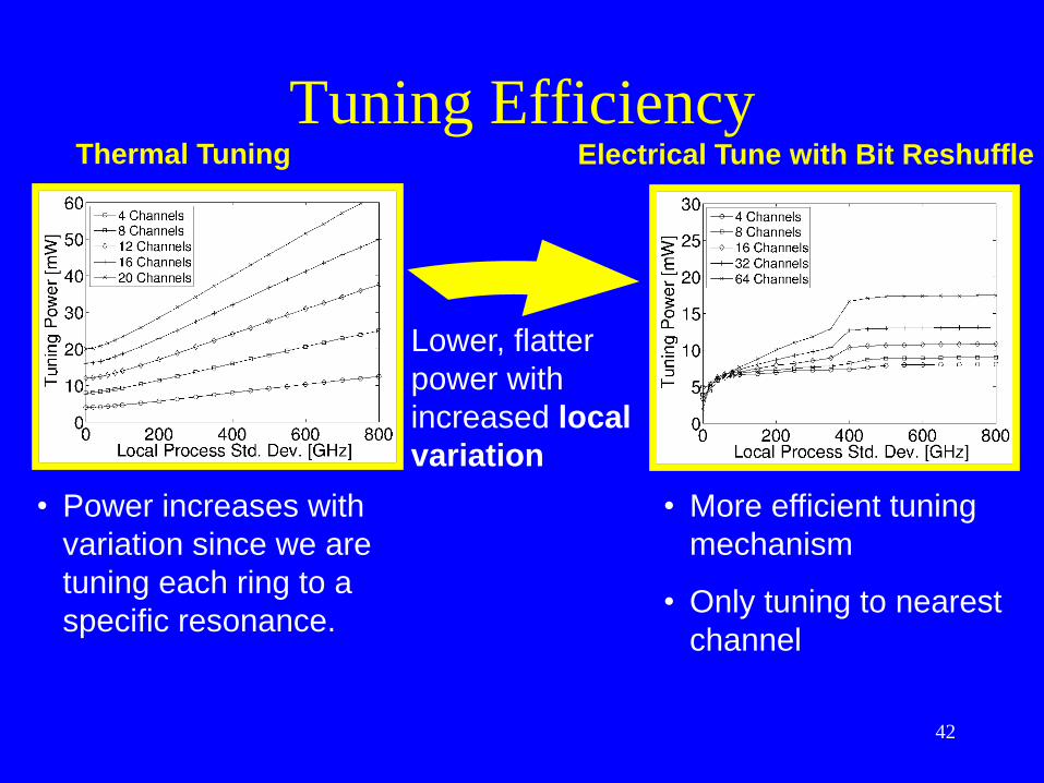
Tuning Efficiency Thermal Tuning
Power increases with
variation since we are
tuning each ring to a
specific resonance.
42
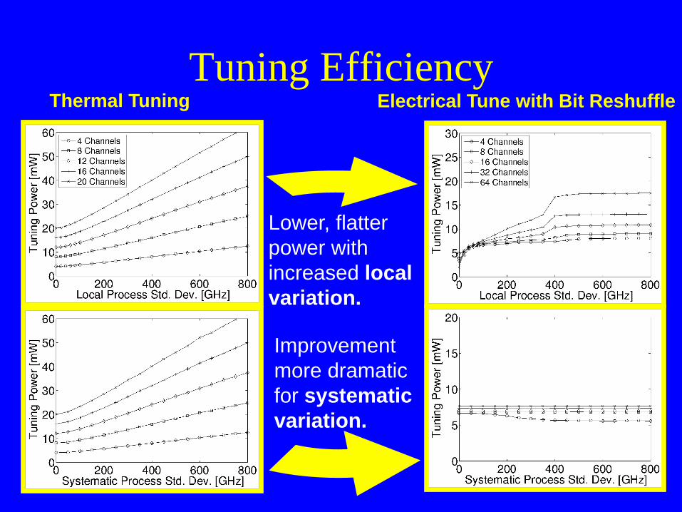
Tuning Efficiency
Lower, flatter
power with
increased local
variation
Thermal Tuning Electrical Tune with Bit Reshuffle
• Power increases with
variation since we are
tuning each ring to a
specific resonance.
• More efficient tuning
mechanism
• Only tuning to nearest
channel
43
Tuning Efficiency Thermal Tuning Electrical Tune with Bit Reshuffle
Improvement
more dramatic
for systematic
variation.
Lower, flatter
power with
increased local
variation.
44
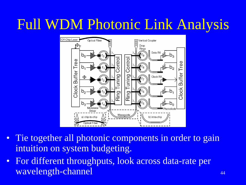
Full WDM Photonic Link Analysis
• Tie together all photonic components in order to gain intuition on system budgeting.
• For different throughputs, look across data-rate per wavelength-channel
45
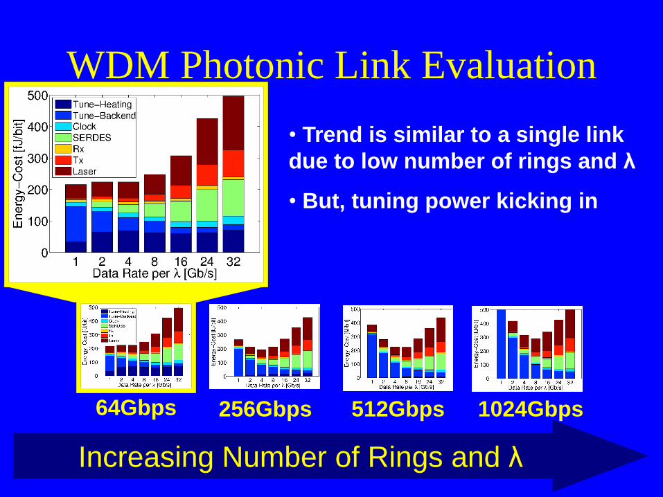
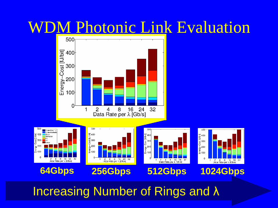
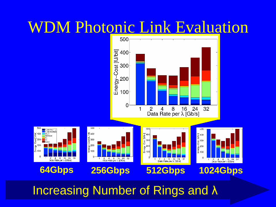
WDM Photonic Link Evaluation
256Gbps 512Gbps 64Gbps
Increasing Number of Rings and λ
1024Gbps
• Trend is similar to a single link
due to low number of rings and λ
• But, tuning power kicking in
46
WDM Photonic Link Evaluation
256Gbps 512Gbps 64Gbps
Increasing Number of Rings and λ
1024Gbps
47
WDM Photonic Link Evaluation
256Gbps 512Gbps 64Gbps
Increasing Number of Rings and λ
1024Gbps
48
WDM Photonic Link Evaluation
256Gbps 512Gbps 64Gbps
Increasing Number of Rings and λ
1024Gbps
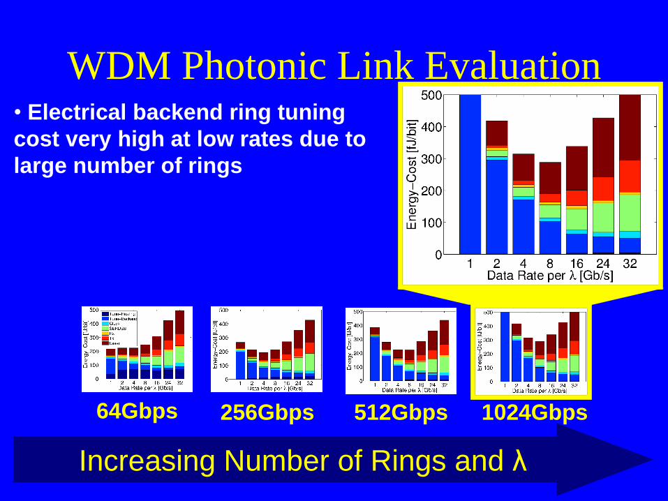
• Electrical backend ring tuning
cost very high at low rates due to
large number of rings
49
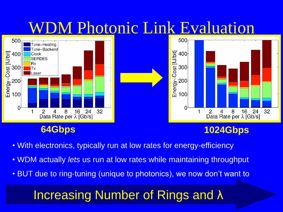
WDM Photonic Link Evaluation
64Gbps
Increasing Number of Rings and λ
1024Gbps
• With electronics, typically run at low rates for energy-efficiency
• WDM actually lets us run at low rates while maintaining throughput
• BUT due to ring-tuning (unique to photonics), we now don’t want to
50
WDM Photonic Link Evaluation
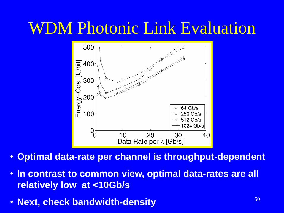
• Optimal data-rate per channel is throughput-dependent
• In contrast to common view, optimal data-rates are all
relatively low at <10Gb/s
• Next, check bandwidth-density
51
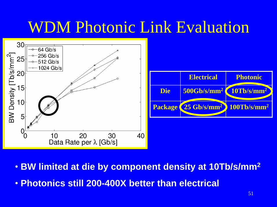
WDM Photonic Link Evaluation
Electrical Photonic
Die 500Gb/s/mm2 10Tb/s/mm2
Package 25 Gb/s/mm2 100Tb/s/mm2
• BW limited at die by component density at 10Tb/s/mm2
• Photonics still 200-400X better than electrical
52
Conclusion
• Photonic interconnects hold promise to meet future compute system communication needs
• To understand photonic system design, we need cross-layer system optimization: – Balance component specifications at the system-level for
best bandwidth-density and energy-efficiency
– Use insight to set the technology trends and device specifications
• Monolithic integration and moderate-data-rate DWDM is most energy-efficient while maintaining significant bandwidth-density advantages.
53
Acknowledgements
• This project is a highly collaborative effort with
teams at MIT, UC Boulder, and UC Berkeley:
– Hanqing Li, Karan Mehta, Jason Orcutt, Jeff Shainline, Jie
Sun, Erman Timurdogan, Stevan Urosevic, Matthew
Weaver, Prof. Milos Popovic, Prof. Rajeev Ram, Prof.
Michael Watts, Prof. Krste Asanovic
• The work was supported in part by MIT CICS,
DARPA, NSF, FCRP IFC, Trusted Foundry, APIC,
Intel, and NSERC.
54
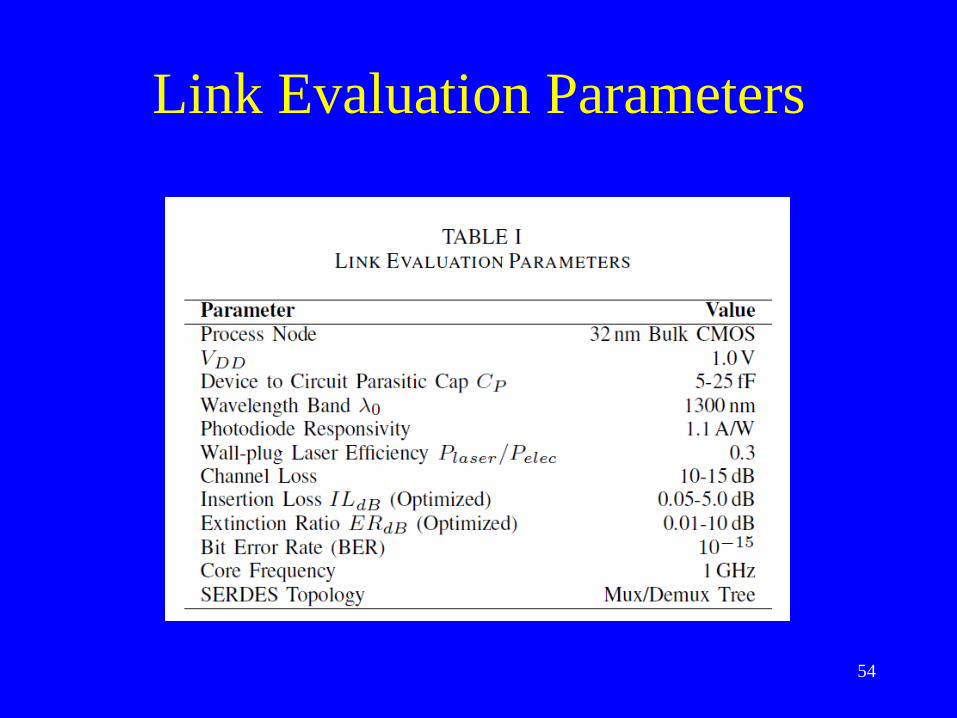
Link Evaluation Parameters