Embed Size (px)
Citation preview

1
SU3B1333C2G9 DDR3-1333(CL9) 204-Pin ECC SO-DIMM
2GB(256M x 72-bit)
ADATA Technology Corp.
Memory Module Data Sheet
DDR3-1333(CL9) 204-Pin ECC SO-DIMM
2GB
(256M x 72-bit)
Version 0.0
Document Number : R11-0853

2
SU3B1333C2G9 DDR3-1333(CL9) 204-Pin ECC SO-DIMM
2GB(256M x 72-bit)
Revision History
Version Changes Page Date
0.0 - Initial release - 2012/3/14

3
SU3B1333C2G9 DDR3-1333(CL9) 204-Pin ECC SO-DIMM
2GB(256M x 72-bit)
Table of Contents
1. General Description .................................................................................... 4
2. Features ..................................................................................................... 4
3. Pin Assignment ................................................................................... ….5~6
4. Pin Description ....................................................................................... 7~8
5. Block Diagram ....................................................................................... 9~10
6. Absolute Maximum Ratings ...................................................................... 11
7. DC Operating Condition .......................................................... ……………11
8. Input DC & AC Logic Level for single-ended signals…………………..…11
9. Input AC Logic Level for single-ended signals…………………………….12
10. IDD Specification……………………………………………………………….13
11.Speed Bins and CL,tRCD,tRP,tRC and tRAS for
Corresponding Bin …………………………………………………………….13
12. Timing Parameters …………..……………………………………………14~15
13. Package Dimensions……………………..……………………………………16
14. Ordering Information…………..……………...…….…………………………17

4
SU3B1333C2G9 DDR3-1333(CL9) 204-Pin ECC SO-DIMM
2GB(256M x 72-bit)
General Description:
The ADATA’s module is a 256Mx72 bit 2GB(2048MB) DDR3-1333(CL9)-9-9-24 SDRAM memory module. The SPD is programmed to JEDEC standard latency 1333Mbps timing of 9-9-9-24 at 1.5V. The module is composed of eight-teen 128Mx8 bit CMOS DDR3 SDRAMs in FBGA package and one 2Kbit EEPROM in 8pin TDFN package on a 204pin glass–epoxy printed circuit board.
The module is a Dual In-line Memory Module and intended for mounting onto 204 pins edge connector sockets. Synchronous design allows precise cycle control with the use of system clock. Data I/O transactions are possible on both edges of DQS. Range of operating frequencies, programmable latencies and burst lengths allow the same device to be useful for a variety of high bandwidth, high performance memory system applications.
Features:
• Power supply (Normal): VDD & VDDQ = 1.5V ± 0.075V • 1.5V (SSTL_15 compatible) I/O • MRS Cycle with address key programs - CAS Latency (5, 6, 7, 8, 9) - Burst Length (BL):8 and 4 with Burst Chop(BC) • Bi-directional, differential data strobe (DQS and /DQS) • Differential clock input (CK, /CK) operation • DLL aligns DQ and DQS transition with CK transition • Double-data-rate architecture; two data transfers per clock cycle • 8 independent internal bank • Internal (self) calibration: Internal self calibration through ZQ pin (RZQ:240 ohm±1%) • Auto refresh and self refresh • Average Refresh Period 7.8us at lower then TCASE 85°C, 3.9us at 85°C < TCASE ≤ 95°C • 8-bit pre-fetch. • On Die Termination using ODT pin. • EEPROM software write protect. • Lead-free and Halogen free products are RoHS Compliant

5
SU3B1333C2G9 DDR3-1333(CL9) 204-Pin ECC SO-DIMM
2GB(256M x 72-bit)
Pin Assignment: 204-PIN SODIMM Front 204-PIN SODIMM Back
PIN Name PIN Name PIN Name PIN Name PIN Name PIN Name PIN Name PIN Name
1 VREFDQ 53 VSS 105 A1 157 DM5 2 VSS 54 DQ28 106 A2 158 VSS
3 VSS 55 DQ24 107 A0 159 DQ42 4 DQ4 56 DQ29 108 BA1 160 DQ46
5 DQ0 57 DQ25 109 VDD 161 DQ43 6 DQ5 58 VSS 110 VDD 162 DQ47
7 DQ1 59 DM3 111 CLK0 163 VSS 8 VSS 60 DQS#3 112 CLK1 164 VSS
9 VSS 61 VSS 113 /CLK0 165 DQ48 10 /DQS0 62 DQ3 114 /CLK1 166 DQ52
11 DM0 63 DQ26 115 VDD 167 DQ49 12 DQS0 64 VSS 116 VDD 168 DQ53
13 DQ2 65 DQ27 117 A10/AP 169 VSS 14 VSS 66 DQ30 118 NC/CS3# 170 VSS
15 DQ3 67 VSS 119 BA0 171 /DQS6 16 DQ6 68 DQ31 120 NC/CS2# 172 DM6
17 VSS 69 CB0 121 WE# 173 DQS6 18 DQ7 70 VSS 122 RAS# 174 DQ54
19 DQ8 71 CB1 123 VDD 175 VSS 20 VSS 72 CB4 124 VDD 176 DQ55
21 DQ9 73 VSS 125 CAS# 177 DQ50 22 DQ12 74 CB5 126 ODT0 178 VSS
23 VSS 75 /DQS8 127 CS0# 179 DQ51 24 DQ13 76 DM8 128 NC/ODT1 180 DQ60
25 /DQS1 77 DQS8 129 NC/CS1# 181 VSS 26 VSS 78 VSS 130 A13 182 DQ61
27 DQS1 79 VSS 131 VDD 183 DQ56 28 DM1 80 CB6 132 VDD 184 VSS
29 VSS 81 CB2 133 DQ32 185 DQ57 30 /RESET 82 CB7 134 DQ36 186 /DQS7
31 DQ10 83 CB3 135 DQ33 187 VSS 32 VSS 84 VREFCA 136 DQ37 188 DQS7
33 DQ11 85 VDD 137 VSS 189 DM7 34 DQ14 86 VDD 138 VSS 190 VSS
35 VSS 87 CKE0 139 DQS4# 191 DQ58 36 DQ15 88 A15 140 DM4 192 DQ62
37 DQ16 89 CKE1 141 DQS4 193 DQ59 38 VSS 90 A14 142 DQ38 194 DQ63
39 DQ17 91 BA2 143 VSS 195 VSS 40 DQ20 92 A9 144 DQ39 196 VSS
41 VSS 93 VDD 145 DQ34 197 SA0 42 DQ21 94 VDD 146 VSS 198 EVENT#
43 /DQS2 95 A12/BC# 147 DQ35 199 VDDSPD 44 DM2 96 A11 148 DQ44 200 SDA
45 DQS2 97 A8 149 VSS 201 SA1 46 VSS 98 A7 150 DQ45 202 SCL

6
SU3B1333C2G9 DDR3-1333(CL9) 204-Pin ECC SO-DIMM
2GB(256M x 72-bit)
47 VSS 99 A5 151 DQ40 203 VTT 48 DQ22 100 A6 152 VSS 204 VTT
49 DQ18 101 VDD 153 DQ41
50 DQ23 102 VDD 154 DQS5#
51 DQ19 103 A3 155 VSS 52 VSS 104 A4 156 DQS5

7
SU3B1333C2G9 DDR3-1333(CL9) 204-Pin ECC SO-DIMM
2GB(256M x 72-bit)
Pin Description:
PIN NAME FUNCTION
CK0~CK1
/CK0~/CK1 System Clock Active on the positive and negative edge to sample all inputs.
CKE0 Clock Enable Masks system clock to freeze operation from the next clock cycle. CKE should be enabled at
least on cycle prior new command. Disable input buffers for power down in standby
/S0~/S1 Chip Select Disables or Enables device operation by masking or enabling all input except CK, CKE and
L(U)DQM
A0~A13 Address Row / Column address are multiplexed on the same pins.
(Row Address: A0~A13 , Column Address: A0~A9 , Auto precharge: A10/AP)
BA0~BA2 Banks Select Selects bank to be activated during row address latch time.
Selects bank for read / write during column address latch time.
DQ0~DQ63
CB0~CB7 Data Data and check bit inputs / outputs are multiplexed on the same pins.
DQS0~DQS8,
/DQS0~/DQS8 Data Strobe Bi-directional Data Strobe
DM0~DM8 Data Mask Mask input data when DM is high.
/RAS Row Address Strobe Latches row addresses on the positive edge of the CK with /RAS low
/CAS Column Address Strobe Latches Column addresses on the positive edge of the CK with /CAS low
/WE Write Enable Enables write operation and row recharge.
VDD / VSS Power Supply/Ground Power and Ground for the input buffers and the core logic.
VREFDQ Power Supply reference Power Supply for reference.DQ,DM.VDD/2
VREFCA Power Supply reference Power Supply for reference. Command , address, & control.VDD/2
VTT Power Supply Termination voltage. Used for address, command & control.VDD/2
VDDSPD SPD Power Supply Serial EEPROM power Supply
SDA Serial data I/O EEPROM serial data I/O

8
SU3B1333C2G9 DDR3-1333(CL9) 204-Pin ECC SO-DIMM
2GB(256M x 72-bit)
SCL Serial clock EEPROM clock input
SA0~SA1 Address in EEPROM EEPROM address input
ODT0,ODT1 On Die Termination When high, termination resistance is enabled for all DQ, /DQ and DM pins, assuming the
function is enabled in the Extended Mode Register Set.
TEST The TEST pin is reserved for bus analysis tools .
/RESET /RESET In Active Low. This signal resets the DDR3 SDRAM
9
SU3B1333C2G9 DDR3-1333(CL9) 204-Pin ECC SO-DIMM
2GB(256M x 72-bit)
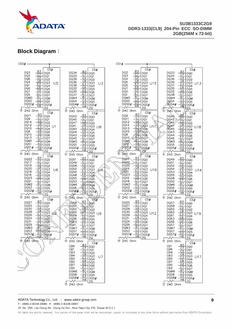
Block Diagram:

10
SU3B1333C2G9 DDR3-1333(CL9) 204-Pin ECC SO-DIMM
2GB(256M x 72-bit)

11
SU3B1333C2G9 DDR3-1333(CL9) 204-Pin ECC SO-DIMM
2GB(256M x 72-bit)
Absolute Maximum Ratings:
Parameter Symbol Value Unit
Voltage on VDD supply relative to Vss VDD -0.4 ~ 1.975 V
Voltage on VDDQ pin relative to Vss VDDQ -0.4 ~1.975 V
Voltage on any pin relative to Vss VIN, Vout -0.4 ~ 1.975 V
Storage temperature TStg -55 ~ +100 ℃
Note: DDR3 SDRAM component specification.
Operation Temperature Condition
Parameter Symbol Value Unit Note
Normal Operating Temperature Range TC 0~+85 ℃ 1
Extended Temperature Range (Optional) TC +85~+95 ℃ 1
Note: (1) If the DRAM case temperature is above 85 ℃, the Auto-Refresh command interval has to be reduced to tREFI=3.9us.
DC Operating Condition:
Voltage referenced to Vss = 0V, VDD&VDDQ=1.5V±0.075V, Tc = 0 to 85 ℃
Parameter Symbol Min Max Unit Note
Supply Voltage VDD 1.425 1.575 V 1,2
VDDSPD 3 3.6 V
Supply Voltage for Output VDDQ 1.425 1.575 V 1,2
I/O Reference Voltage(CMD/ADD) VREFCA, (DC) 0.49 x VDDQ 0.51 x VDDQ V 3,4
I/O Reference Voltage(DQ) VREFDQ, (DC) 0.49 x VDDQ 0.51 x VDDQ V 3,4
Termination Voltage VTT VDDQ/2 VDDQ/2 V
Note: (1) Under all conditions VDDQ must be less than or equal to VDD.
(2) VDDQ tracks with VDD. AC parameters are measured with VDD and VDDQ tied together.
(3) The AC peak noise on VREF may not allow VREF to deviate from VREF(DC) by more than ±1% VDD
(for reference: approx. ±15mV)
(4) For reference: approx. VDD/2 ±15mV

12
SU3B1333C2G9 DDR3-1333(CL9) 204-Pin ECC SO-DIMM
2GB(256M x 72-bit)
Input DC & AC Logic Level for single-ended signals:
Parameter Symbol Min Max Unit Note
DC Input logic high voltage VIH (DC) VREF+100 VDD mV 1
DC Input logic low voltage VIL (DC) VSS VREF-100 mV 1
AC input logic high VIH(AC) VREF + 175 - mV 1,2
AC input logic low VIL(AC) - VREF – 175 mV 1,2
Note: 1. For DQ and DM, VREF = VREFDQ . For input only pins except RESET, or VREF = VREFCA.
2. See "Overshoot and Undershoot specifications" on component datasheet
Input AC Logic Level for single-ended signals:
Parameter Symbol Min Max Unit Note
Differential input high VIHdiff +0.2 Note 3 V 1
Differential input low VILdiff Note 3 -0.2 V 1
Differential input high AC VIHdiff(AC) 2 (VIH(ac)-Vref) Note 3 V 2
Differential input low AC VILdiff (AC) Note 3 2 x (Vref - VIL(ac)) V 2
Notes: 1. Used to define a differential signal slew-rate.
2. For CK - CK use VIH/VIL(ac) of ADD/CMD and VREFCA; for DQS - DQS, DQSL - DQSL, DQSU - DQSU use VIH/VIL(ac) of DQs
and VREFDQ; if a reduced ac-high or ac-low level is used for a signal group, then the reduced level applies also here.
3. These values are not defined, however they single-ended signals CK, /CK, DQS, /DQS, DQSL, /DQSL, DQSU, /DQSU need to be
within the respective limits (VIH(dc) max, VIL(dc)min) for single-ended signals as well as the limitations for overshoot and undershoot
on Component Datasheet.

13
SU3B1333C2G9 DDR3-1333(CL9) 204-Pin ECC SO-DIMM
2GB(256M x 72-bit)
IDD Specification:
Symbol Condition Typical Unit
IDD0 Operating One Bank Active-Precharge Current 603 mA
IDD1 Operating One Bank Active-Read-Precharge Current 738 mA
IDD2P0 Precharge Power-Down Current Slow Exit 216 mA
IDD2P1 Precharge Power-Down Current Fast Exit 504 mA
IDD2Q Precharge Quiet Standby Current 504 mA
IDD2N Precharge Standby Current 540 mA
IDD3P Active Power-Down Current 756 mA
IDD3N Active Standby Current 846 mA
IDD4W Operating Burst Write Current 1098 mA
IDD4R Operating Burst Read Current 1233 mA
IDD5B Burst Refresh Current 1773 mA
IDD6 Self Refresh Current: Normal Temperature Range 126 mA
IDD7 Operating Bank Interleave Read Current 1953 mA
Note: IDD current measure method and detail patterns are described on DDR3 component datasheet. Only for reference.
Speed Bins and CL,tRCD,tRP,tRC and tRAS for Corresponding Bin:
Speed DDR3-1333
Units Bin(CL-tRCD-tRP) 9-9-9
Parameter Min
CL 9 tCK
tRCD 13.125 ns
tRC 49.125 ns
tRRD 6 ns
tCK 1.5 ns
tRAS 36 ns
tRP 13.125 ns
tRFC 160 Ns
14
SU3B1333C2G9 DDR3-1333(CL9) 204-Pin ECC SO-DIMM
2GB(256M x 72-bit)
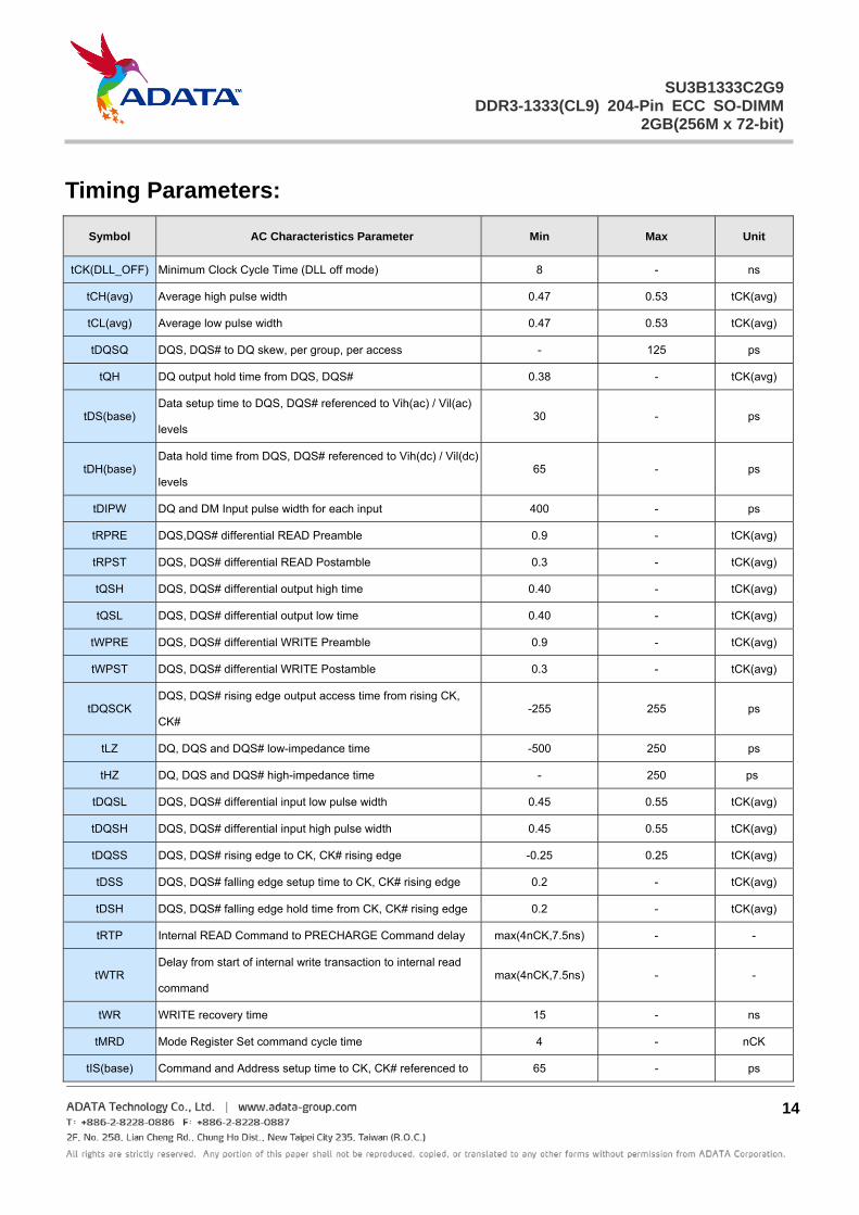
Timing Parameters:
Symbol AC Characteristics Parameter Min Max Unit
tCK(DLL_OFF) Minimum Clock Cycle Time (DLL off mode) 8 - ns
tCH(avg) Average high pulse width 0.47 0.53 tCK(avg)
tCL(avg) Average low pulse width 0.47 0.53 tCK(avg)
tDQSQ DQS, DQS# to DQ skew, per group, per access - 125 ps
tQH DQ output hold time from DQS, DQS# 0.38 - tCK(avg)
tDS(base) Data setup time to DQS, DQS# referenced to Vih(ac) / Vil(ac)
levels 30 - ps
tDH(base) Data hold time from DQS, DQS# referenced to Vih(dc) / Vil(dc)
levels 65 - ps
tDIPW DQ and DM Input pulse width for each input 400 - ps
tRPRE DQS,DQS# differential READ Preamble 0.9 - tCK(avg)
tRPST DQS, DQS# differential READ Postamble 0.3 - tCK(avg)
tQSH DQS, DQS# differential output high time 0.40 - tCK(avg)
tQSL DQS, DQS# differential output low time 0.40 - tCK(avg)
tWPRE DQS, DQS# differential WRITE Preamble 0.9 - tCK(avg)
tWPST DQS, DQS# differential WRITE Postamble 0.3 - tCK(avg)
tDQSCK DQS, DQS# rising edge output access time from rising CK,
CK# -255 255 ps
tLZ DQ, DQS and DQS# low-impedance time -500 250 ps
tHZ DQ, DQS and DQS# high-impedance time - 250 ps
tDQSL DQS, DQS# differential input low pulse width 0.45 0.55 tCK(avg)
tDQSH DQS, DQS# differential input high pulse width 0.45 0.55 tCK(avg)
tDQSS DQS, DQS# rising edge to CK, CK# rising edge -0.25 0.25 tCK(avg)
tDSS DQS, DQS# falling edge setup time to CK, CK# rising edge 0.2 - tCK(avg)
tDSH DQS, DQS# falling edge hold time from CK, CK# rising edge 0.2 - tCK(avg)
tRTP Internal READ Command to PRECHARGE Command delay max(4nCK,7.5ns) - -
tWTR Delay from start of internal write transaction to internal read
command max(4nCK,7.5ns) - -
tWR WRITE recovery time 15 - ns
tMRD Mode Register Set command cycle time 4 - nCK
tIS(base) Command and Address setup time to CK, CK# referenced to 65 - ps
15
SU3B1333C2G9 DDR3-1333(CL9) 204-Pin ECC SO-DIMM
2GB(256M x 72-bit)
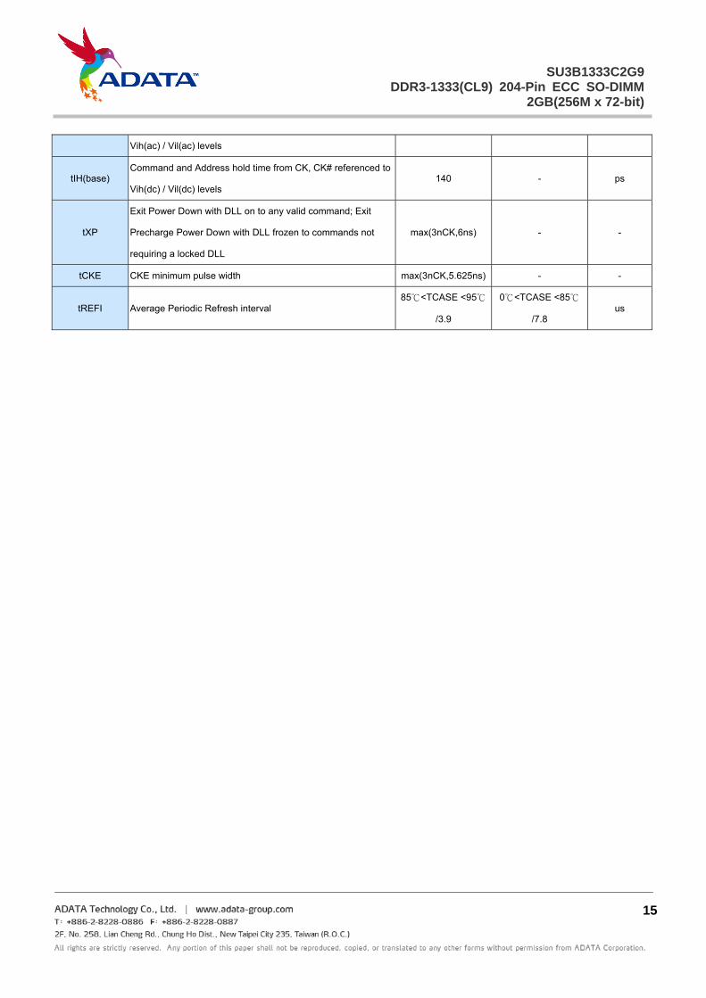
Vih(ac) / Vil(ac) levels
tIH(base) Command and Address hold time from CK, CK# referenced to
Vih(dc) / Vil(dc) levels 140 - ps
tXP
Exit Power Down with DLL on to any valid command; Exit
Precharge Power Down with DLL frozen to commands not
requiring a locked DLL
max(3nCK,6ns) - -
tCKE CKE minimum pulse width max(3nCK,5.625ns) - -
tREFI Average Periodic Refresh interval 85℃<TCASE <95℃
/3.9
0℃<TCASE <85℃
/7.8 us

16
SU3B1333C2G9 DDR3-1333(CL9) 204-Pin ECC SO-DIMM
2GB(256M x 72-bit)
Package Dimensions:

17
SU3B1333C2G9 DDR3-1333(CL9) 204-Pin ECC SO-DIMM
2GB(256M x 72-bit)
Ordering Information:
SU 3 B 1 3 3 3 C 2G 9 X X X 1-2 3 4 5-8 9 1011 12 13-15
1-2. Brand+Family Code 9. Component Config Code
SU: ADATA C:256MX8
3. Generation 10-11. Capacity
3: DDR3 2G: 2GB
D: DDR3L 4G: 4GB
4. DRAM Type 12. CAS Latency
B: ECC SO-DIMM 9: CL9
11: CL11
5-8. Clock Speed
1333: 1333MHz 13-15. Package Code