Embed Size (px)
Citation preview

UCLAUCLA Electronic Theses and Dissertations
TitleAdaptive Techniques for Mitigating Circuit Imperfections in High Performance A/D Converters
Permalinkhttps://escholarship.org/uc/item/30h4w602
AuthorTing, Shang Kee
Publication Date2014-01-01 Peer reviewed|Thesis/dissertation
eScholarship.org Powered by the California Digital LibraryUniversity of California

University of California
Los Angeles
Adaptive Techniques for Mitigating Circuit
Imperfections in High Performance A/D
Converters
A dissertation submitted in partial satisfaction of the
requirements for the degree Doctor of Philosophy
in Electrical Engineering
by
Shang Kee Ting
2014

c© Copyright by
Shang Kee Ting
2014
Abstract of the Dissertation
Adaptive Techniques for Mitigating Circuit
Imperfections in High Performance A/D
Converters
by
Shang Kee Ting
Doctor of Philosophy in Electrical Engineering
University of California, Los Angeles, 2014
Professor Ali H. Sayed, Chair
In this dissertation, we examine the effect of four sources of circuit imperfec-
tions on the performance of analog-to-digital converters (ADCs), including sam-
pling clock jitters, spurious sidebands, timing mismatches, and gain mismatches.
These imperfections distort the sampled data and degrade the signal-to-noise ra-
tio (SNR) of the ADCs. We develop signal models for the distortions and propose
effective adaptive signal processing techniques to filter the sampled data and mit-
igate the spurious effects. Rather than remove the distortions by perfecting the
circuitry, the proposed techniques focus on processing the sampled data by using
adaptive DSP algorithms.
Analog circuit impairments create many distortions including I/Q imbalances,
phase noise, frequency offsets, and sampling clock jitter. Timing jitters generally
arise from noise in the clock generating crystal and phase-locked-loop (PLL). The
jitters cause the ADCs to sample the input signals at non-uniform sampling times
and introduce distortion that limits the signal fidelity and degrades the SNR.
While the effects of jitter noise can be neglected at low frequencies, applications
ii
requiring enhanced performance at higher frequencies demand higher SNR from
the sampling circuit. We first examine the effect of the clock jitter on the SNR
of the sampled signal and subsequently propose compensation methods based on
a signal injection structure for direct down-conversion architectures.
We also address the effect of non-ideal PLL circuitry on the quality of the
sampled data. In a non-ideal PLL circuit, leakage of the reference signal into
the control line produces spurious tones. When the distorted PLL signal is used
to generate the sampling clock, it injects the spurious tones into the sampled
data. These distortions are harmful for wideband applications, such as spectrum
sensing, since they affect the detection of vacant frequency bands. We again
examine the distortion effect in some detail and propose techniques in the digital
domain to clean the data and remove the PLL leakage effects. We study the
performance of the proposed algorithms and compare it against the corresponding
Cramer-Rao bound (CRB).
We further propose an adaptive frequency-domain structure to compensate
the effect of timing and gain mismatches in time-interleaved ADCs. An M-
channel time-interleaved ADC uses M ADCs to sample an input signal to obtain a
larger effective sampling rate. However, in practice, combining ADCs introduces
mismatches among the various ADC channels. In the proposed solution, the
signal is split into multiple frequency bins and adaptation across the frequency
channels is combined by means of an adaptive strategy. The construction is able
to assign more or less weight to the various frequency channels depending on
whether their estimates are more or less reliable in comparison to other channels.
iii

The dissertation of Shang Kee Ting is approved.
Robert M’Closkey
Danijela Cabric
Dejan Markovic
Ali H. Sayed, Committee Chair
University of California, Los Angeles
2014
iv

Table of Contents
1 Introduction . . . . . . . . . . . . . . . . . . . . . . . . . . . . . . . . 1
1.1 Imperfections in analog-to-digital conversion . . . . . . . . . . . . 1
1.2 Contributions . . . . . . . . . . . . . . . . . . . . . . . . . . . . . 3
1.3 Organization . . . . . . . . . . . . . . . . . . . . . . . . . . . . . 4
2 Digital Suppression of Spurious PLL Tones in ADCs . . . . . . 6
2.1 Effect of leakage on the clock signal . . . . . . . . . . . . . . . . . 9
2.1.1 Source of leakage . . . . . . . . . . . . . . . . . . . . . . . 9
2.1.2 Effect of leakage . . . . . . . . . . . . . . . . . . . . . . . . 11
2.2 Non-ideal sampling and distortion model . . . . . . . . . . . . . . 12
2.2.1 Sampling instants . . . . . . . . . . . . . . . . . . . . . . . 12
2.2.2 Accuracy of model . . . . . . . . . . . . . . . . . . . . . . 13
2.3 Effect of sampling distortions on ADC performance . . . . . . . . 14
2.4 Sideband suppression . . . . . . . . . . . . . . . . . . . . . . . . . 16
2.4.1 Training signal injection . . . . . . . . . . . . . . . . . . . 18
2.4.2 Training signal extraction . . . . . . . . . . . . . . . . . . 19
2.4.3 Signal recovery . . . . . . . . . . . . . . . . . . . . . . . . 21
2.5 Parameter and offset estimation . . . . . . . . . . . . . . . . . . . 23
2.5.1 Estimation algorithm . . . . . . . . . . . . . . . . . . . . . 23
2.5.2 Cramer-Rao bound . . . . . . . . . . . . . . . . . . . . . . 27
2.5.3 Performance analysis . . . . . . . . . . . . . . . . . . . . . 32
v

2.6 Simulations . . . . . . . . . . . . . . . . . . . . . . . . . . . . . . 34
2.6.1 Effect of bit resolution . . . . . . . . . . . . . . . . . . . . 34
2.6.2 Effect of increasing the amplitude of the training signal . . 38
2.6.3 Effect of additional random jitter in ADC . . . . . . . . . 39
2.6.4 Effect of noise in training signal . . . . . . . . . . . . . . . 41
2.7 Conclusion . . . . . . . . . . . . . . . . . . . . . . . . . . . . . . . 41
2.A Derivation of relative error bounds . . . . . . . . . . . . . . . . . 42
2.B Modeling of phase noise in second-order PLL . . . . . . . . . . . . 45
2.C Effect of jitter in y(n) on training signal extraction . . . . . . . . 46
2.D Phase estimation . . . . . . . . . . . . . . . . . . . . . . . . . . . 47
3 Compensating Spurious PLL Tones in Spectrum Sensing Archi-
tectures . . . . . . . . . . . . . . . . . . . . . . . . . . . . . . . . . . . . 49
3.1 Effects of leakage from reference signal . . . . . . . . . . . . . . . 51
3.1.1 Reference leakage in PLL . . . . . . . . . . . . . . . . . . . 51
3.1.2 Effect of leakage on the sampling clock of the ADC . . . . 53
3.1.3 Effect of distorted sampling offsets on training signal . . . 55
3.1.4 Effects of the spurious sidebands on spectrum sensing . . . 57
3.2 Proposed solution . . . . . . . . . . . . . . . . . . . . . . . . . . . 58
3.2.1 TFT algorithm . . . . . . . . . . . . . . . . . . . . . . . . 58
3.2.2 Block diagram of TFT . . . . . . . . . . . . . . . . . . . . 61
3.2.3 FOT algorithm . . . . . . . . . . . . . . . . . . . . . . . . 64
3.3 Detection of signals using an energy detector . . . . . . . . . . . . 66
vi

3.3.1 No signal of interest - H0 . . . . . . . . . . . . . . . . . . . 68
3.3.2 Sinusoidal tone- H1 . . . . . . . . . . . . . . . . . . . . . . 68
3.3.3 Sinusoidal tone in the presence of strong interfering tone
from a neighboring band - H′1 . . . . . . . . . . . . . . . . 70
3.3.4 Unknown white signals - H2 and H′2 . . . . . . . . . . . . 72
3.4 Simulations . . . . . . . . . . . . . . . . . . . . . . . . . . . . . . 73
3.4.1 Sideband suppression . . . . . . . . . . . . . . . . . . . . . 74
3.4.2 Detection performance - H1 and H′1 . . . . . . . . . . . . . 75
3.4.3 Detection performance - H2 and H′2 . . . . . . . . . . . . . 77
3.4.4 Impact of threshold during sensing . . . . . . . . . . . . . 79
3.5 Conclusion . . . . . . . . . . . . . . . . . . . . . . . . . . . . . . . 81
3.A Energy detector for signals with fixed power . . . . . . . . . . . . 82
3.A.1 Noncentral chi-square for circular complex variables . . . . 82
3.A.2 Energy detector for signals with a fixed power . . . . . . . 83
3.B Comparison of various compensation schemes . . . . . . . . . . . 84
3.C Increasing sensing time . . . . . . . . . . . . . . . . . . . . . . . . 89
4 Clock Jitter Compensation in High-Rate ADC Circuits . . . . 90
4.1 Problem formulation . . . . . . . . . . . . . . . . . . . . . . . . . 92
4.1.1 Stochastic properties of the clock jitter . . . . . . . . . . . 94
4.1.2 Effects of the clock jitter . . . . . . . . . . . . . . . . . . . 98
4.2 Estimation of clock jitter . . . . . . . . . . . . . . . . . . . . . . . 103
4.2.1 Direct downconversion receiver . . . . . . . . . . . . . . . 105
vii

4.2.2 Direct jitter estimation . . . . . . . . . . . . . . . . . . . . 107
4.2.3 Adaptive jitter estimation . . . . . . . . . . . . . . . . . . 109
4.3 Compensation of clock jitter . . . . . . . . . . . . . . . . . . . . . 112
4.4 Mean-square-error analysis . . . . . . . . . . . . . . . . . . . . . . 114
4.4.1 Direct estimation method . . . . . . . . . . . . . . . . . . 114
4.4.2 Adaptive estimation methods . . . . . . . . . . . . . . . . 116
4.5 SNR analysis . . . . . . . . . . . . . . . . . . . . . . . . . . . . . 118
4.6 Simulation results . . . . . . . . . . . . . . . . . . . . . . . . . . . 120
4.7 Concluding remarks . . . . . . . . . . . . . . . . . . . . . . . . . . 123
4.A Stochastic properties of jitter . . . . . . . . . . . . . . . . . . . . 123
4.B Derivation of phase-noise PSD . . . . . . . . . . . . . . . . . . . . 126
4.C Effective signal-to-noise ratio (ESNR) . . . . . . . . . . . . . . . . 128
4.D Clock recovery . . . . . . . . . . . . . . . . . . . . . . . . . . . . . 129
4.E Power of N -th derivative of box-car random signal . . . . . . . . . 130
4.F Bounding the power of the derivative of a random signal . . . . . 131
5 Compensating Mismatches in Time-Interleaved A/D Converters133
5.1 Problem formulation . . . . . . . . . . . . . . . . . . . . . . . . . 136
5.2 Existing techniques and limitations . . . . . . . . . . . . . . . . . 138
5.2.1 Linear approximation . . . . . . . . . . . . . . . . . . . . . 138
5.2.2 Compensation . . . . . . . . . . . . . . . . . . . . . . . . . 141
5.2.3 Limitations . . . . . . . . . . . . . . . . . . . . . . . . . . 143
5.3 Proposed solutions . . . . . . . . . . . . . . . . . . . . . . . . . . 144
viii

5.3.1 Time-domain solution . . . . . . . . . . . . . . . . . . . . 144
5.3.2 Frequency-domain solution . . . . . . . . . . . . . . . . . . 147
5.3.3 Enhanced frequency-domain solution . . . . . . . . . . . . 158
5.4 Comparison with prior work . . . . . . . . . . . . . . . . . . . . . 165
5.5 Performance analysis . . . . . . . . . . . . . . . . . . . . . . . . . 169
5.5.1 Assumptions on the signal and its distortions . . . . . . . 169
5.5.2 Statistical properties of data model . . . . . . . . . . . . . 170
5.5.3 MSD and SNR measures . . . . . . . . . . . . . . . . . . . 172
5.5.4 Error recursions . . . . . . . . . . . . . . . . . . . . . . . . 173
5.5.5 Combination weights and stepsizes . . . . . . . . . . . . . 177
5.5.6 Convergence in mean . . . . . . . . . . . . . . . . . . . . . 178
5.5.7 Mean square stability . . . . . . . . . . . . . . . . . . . . . 179
5.5.8 MSD and EMSE . . . . . . . . . . . . . . . . . . . . . . . 180
5.6 Simulations results . . . . . . . . . . . . . . . . . . . . . . . . . . 181
5.6.1 MSD and SNR measures . . . . . . . . . . . . . . . . . . . 182
5.6.2 Comparing with prior works . . . . . . . . . . . . . . . . . 183
5.6.3 Performance measures using MSD and SNR . . . . . . . . 191
5.7 Discussion and conclusion . . . . . . . . . . . . . . . . . . . . . . 194
5.A Proof for mean convergence . . . . . . . . . . . . . . . . . . . . . 195
5.B Proof for (5.1) . . . . . . . . . . . . . . . . . . . . . . . . . . . . . 199
6 Conclusion and Future Research . . . . . . . . . . . . . . . . . . . 205
References . . . . . . . . . . . . . . . . . . . . . . . . . . . . . . . . . . . 207
ix

List of Figures
2.1 Block diagram of a PLL. . . . . . . . . . . . . . . . . . . . . . . . 10
2.2 PSD of distorted PLL clock and sampled sinusoid. . . . . . . . . . 16
2.3 Proposed architecture for reducing the effect of PLL sidebands on
A/D converters. . . . . . . . . . . . . . . . . . . . . . . . . . . . . 17
2.4 PSD of wm[n] cos(2πfynTs + θy). . . . . . . . . . . . . . . . . . . . 20
2.5 Diagram of signal extraction block. . . . . . . . . . . . . . . . . . 21
2.6 Block diagram of the signal recovery. . . . . . . . . . . . . . . . . 22
2.7 Normalized MSE and CRB bound of the sampling offset estimates. 33
2.8 RPSI of spurious sidebands in a 10 bit sampled signal. . . . . . . 35
2.9 RPSI of spurious sidebands in a 16 bit sampled signal. . . . . . . 35
2.10 RPSI of spurious sidebands vs bit resolutions. . . . . . . . . . . . 36
2.11 MSE of sampling offset estimates vs bit resolutions. . . . . . . . . 37
2.12 Effect of increasing the amplitude of the training signal. . . . . . . 38
2.13 RPSI of spurious sidebands vs amplitude of training signal. . . . . 39
2.14 PSD of a tone when σADC in the ADC is 0.5%. . . . . . . . . . . 40
2.15 PSD of a tone when σADC in the ADC is 1%. . . . . . . . . . . . 41
2.16 RPSI of spurious sideband vs input training frequency with σADC =
1%. . . . . . . . . . . . . . . . . . . . . . . . . . . . . . . . . . . . 42
2.17 RPSI of spurious sideband as σADC is varied. . . . . . . . . . . . . 43
2.18 RPSI of spurious sideband as σLF is varied. . . . . . . . . . . . . . 43
3.1 Block diagram of a PLL. . . . . . . . . . . . . . . . . . . . . . . . 52
x

3.2 PSD of distorting training signal. . . . . . . . . . . . . . . . . . . 56
3.3 Proposed architecture for reducing the effects of PLL sidebands in
spectrum sensing applications. . . . . . . . . . . . . . . . . . . . . 58
3.4 PSD of frequency channel when windowing is used. . . . . . . . . 61
3.5 Block diagram of the TFT algorithm. . . . . . . . . . . . . . . . . 63
3.6 Block diagram of STFT. . . . . . . . . . . . . . . . . . . . . . . . 63
3.7 Block diagram of Apk block. . . . . . . . . . . . . . . . . . . . . . 64
3.8 Block diagram of Bfk block. . . . . . . . . . . . . . . . . . . . . . 64
3.9 Block diagram of the FOT algorithm. . . . . . . . . . . . . . . . . 66
3.10 Frequency response of the derivative filter. . . . . . . . . . . . . . 67
3.11 PSD of signal before and after compensation. . . . . . . . . . . . 75
3.12 Sideband suppression performance as length of data is increased. . 76
3.13 PD vs PFA of the weak sinusoidal signal in presence of a strong
sinusoidal signal. . . . . . . . . . . . . . . . . . . . . . . . . . . . 78
3.14 PD vs PFA of the weak QPSK signal in presence of a strong QPSK
signal. . . . . . . . . . . . . . . . . . . . . . . . . . . . . . . . . . 79
3.15 The plots show the normalized threshold used to obtain the various
pairs of PD amd PFA for sinusoidal signals H1. . . . . . . . . . . 80
3.16 Impact of thresholding on PD amd PFA. . . . . . . . . . . . . . . 81
3.17 PSD of distorted and compensated signal using various algorithms
with small sampling offsets. . . . . . . . . . . . . . . . . . . . . . 87
3.18 PSD of distorted and compensated signal using various algorithms
with larger sampling offsets. . . . . . . . . . . . . . . . . . . . . . 88
xi

3.19 PD vs PFA of the weak sinusoidal signal in presence of a strong
sinusoidal signal. . . . . . . . . . . . . . . . . . . . . . . . . . . . 89
4.1 In-phase and quadrature phase components of a complex-valued
signal r(t) sampled by a pair of ADCs. . . . . . . . . . . . . . . . 93
4.2 The PSD of the jitter using fe = 5MHz, fs = 1GHz as well as the
expected amount of jitter reduction as a function of ωcut. . . . . . 96
4.3 Relationship between SNR and σe for complex-sinusoidal signals
and bandlimited signals. . . . . . . . . . . . . . . . . . . . . . . . 100
4.4 Proposed signal injection architecture used for jitter estimation. . 105
4.5 High-frequency injection model. . . . . . . . . . . . . . . . . . . . 108
4.6 Jitter recovery structure based on (4.35). . . . . . . . . . . . . . . 109
4.7 Adaptive jitter recovery structure based on (4.40)–(4.43) . . . . . 112
4.8 Proposed compensation algorithm (4.49). . . . . . . . . . . . . . . 114
4.9 MSE model for e[n] . . . . . . . . . . . . . . . . . . . . . . . . . . 116
4.10 Phase domain model of adaptive jitter recovery algorithm . . . . . 117
4.11 Linear system model for adaptive jitter recovery during jitter-
tracking operation. . . . . . . . . . . . . . . . . . . . . . . . . . . 118
4.12 Normalized PSD of input signal r[n] used in the simulation. . . . 121
4.13 In (a), we illustrate the simulated and theoretical MSE in the
estimation of the jitter using the direct and adaptive techniques. In
(b), we illustrate the expected SNR as a result of jitter compensation.122
4.14 PLL phase model used to derive PSD of PLL output phase-noise . 126
4.15 Block diagram of the phase-locked-loop . . . . . . . . . . . . . . . 130
xii
5.1 M-Channel TI-ADC with gain and timing mismatches. . . . . . . 137
5.2 Sample spectra of a 2-channel and 4-channel TI-ADC. . . . . . . . 138
5.3 Structure used in reference [1]. . . . . . . . . . . . . . . . . . . . . 141
5.4 Spectra of a oversampled signal showing the assumptions used in
reference [1]. . . . . . . . . . . . . . . . . . . . . . . . . . . . . . . 142
5.5 Spectra of input signals that breaks the assumptions in reference [1].143
5.6 An adaptive structure for interference cancelation. . . . . . . . . . 145
5.7 Block diagram representation of the proposed time-domain solution.146
5.8 Block diagram representation of the frequency-domain solution. . 146
5.9 Mesh network representing the interactions among all N frequency
bins for k = 0, 1, . . . , N − 1. . . . . . . . . . . . . . . . . . . . . . 151
5.10 Example of PZ [k] and PZ [k] + PZ [k] for a low-pass signal in noise. 155
5.11 Illustration for the motivation behind the the proposed combina-
tion weights. . . . . . . . . . . . . . . . . . . . . . . . . . . . . . . 156
5.12 Block diagram representation of the frequency-domain solution
based on a second-order compensation stage. . . . . . . . . . . . . 161
5.13 Block diagram representation of algorithm in reference [2]. . . . . 167
5.14 Comparing the various algorithms on a low-pass signal. . . . . . . 186
5.15 Spectra of distorted and recovered signals. . . . . . . . . . . . . . 187
5.16 Comparing the various algorithms on a band-pass signal. . . . . . 189
5.17 Comparing the various algorithms on a band-pass signal by ad-
justing the stepsizes. . . . . . . . . . . . . . . . . . . . . . . . . . 191
5.18 MSD and SNR performance (when first-order distortion is removed)
as the bandwidth of a low-pass signal is varied. . . . . . . . . . . 192
xiii

5.19 MSD and SNR performance (when both first-order and second-
order distortion are removed) as the bandwidth of a low-pass signal
is varied. . . . . . . . . . . . . . . . . . . . . . . . . . . . . . . . . 194
5.20 MSD and SNR performance (when first-order distortion is removed)
as the bandwidth of a band-pass signal is varied. . . . . . . . . . . 195
5.21 MSD and SNR performance (when both first-order and second-
order distortion are removed) as the bandwidth of a band-pass
signal is varied. . . . . . . . . . . . . . . . . . . . . . . . . . . . . 196
xiv

List of Tables
2.1 Filter coefficients of a FIR differentiator filter. . . . . . . . . . . . 22
4.1 Table listing the default values for parameters in the simulation . 120
5.1 SNR of the distorted and recovered low-pass signal. . . . . . . . . 185
5.2 SNR of the distorted and recovered band-pass signal. . . . . . . . 188
5.3 SNR of the distorted and recovered band-pass signal after reducing
the stepsizes for the time-domain solution and Matsuno’s solution. 190
xv
List of Algorithms
2.1 Summary of sideband suppression algorithm . . . . . . . . . . . . 23
2.2 Parameter estimation algorithm . . . . . . . . . . . . . . . . . . . 28
2.3 Simplified parameter estimation algorithm . . . . . . . . . . . . . 29
3.1 Summary of TFT algorithm . . . . . . . . . . . . . . . . . . . . . 62
5.1 Summary of frequency-domain solution . . . . . . . . . . . . . . . . 159
5.1A Stage A1: first-order compensation algorithm . . . . . . . . . . . . . 159
5.1B Stage B: interference cancelation algorithm . . . . . . . . . . . . . . 160
5.2 Summary of enhanced frequency-domain solution . . . . . . . . . . . 165
5.2A Stage A2: second-order compensation algorithm . . . . . . . . . . . . 166
xvi

Acknowledgments
I would like to thank my advisor, Professor Ali H. Sayed, for his guidance during
my Ph.D. program. His careful reading and critique of my work helped me dig
deeper and improve the results on a continual basis.
Next, I would like to acknowledge the members and visitors of the Adaptive
Systems Laboratory. I learned a lot from them, and they have provided lots of
good advice and inspiration. I will remember the times when we – Zaid Towfic,
Sheng-yuan Tu, Jianshu Chen, Xiaochuan Zhao, and Chung-Kai Yu – went for
group outings, house-warming, and Turkey dinners. I would also like to thank
some past members from the lab – Federico Cattivelli, Qiyue Zou and Zhi Quan,
who helped me during my first year. It was also great to meet the visiting
scholars who passed by our lab - Jesus F. Bes, Mohammad Reza Gholami, Sergio
Valcarcel-Macua, Milad A. Toutounchian, Reza Abdolee, Jae-Woo Lee, Victor
Lora, Paolo Di Lorenzo, Alexander Bertrand, Oyvind L. Rortveit, Hongyang
Chen, Jingon Joung, Eva Hamou, Henri Pesonen, and Noriyuki Takahashi.
I would also like to thank my family for everything they have done over the
years. Firstly, my parents who brought me up and supported me. My Dad who
gave me a head-start in Mathematics, and my Mom who gave me lots of love
and encouragement. I am sad that Mom departed during my studies, but I will
always remember her. Also, my brothers who took care of my parents while I
was not around. Finally, I am very grateful to have a loving and supportive wife,
Lee Ngee. Although the journey towards our PhDs has been challenging, I am
lucky that we are accompanying each other through it. Moreover, it is really
amazing that our daughter, Clare, was born during this journey. Let us continue
our journey together hand-in-hand.
xvii
Vita
1976 Born, Singapore.
2001 B.S. (Electrical Engineering), National University of Singapore
(NUS), Singapore.
2002 M.S. (High Performance Computation for Engineered Systems),
NUS.
2002–2008 Senior Member of Technical Staff, DSO, Singapore.
2008–present PhD Candidate, Department of Electrical Engineering, Univer-
sity of California, Los Angeles, USA.
xviii

CHAPTER 1
Introduction
1.1 Imperfections in analog-to-digital conversion
One of the key components in radio and communication devices is the analog-
to-digital converter (ADC). In modern communication systems, there is a trend
to miniaturize radio devices and, yet, increase their flexibility to handle higher
carrier frequencies and larger bandwidths. For example, certain applications of
modern radios, such as cognitive radios and UWB radios [3], may require ADCs
operating at high sampling rates due to the use of wide frequency bands. However,
these circuit requirements are generally hard to meet in current practice and
have cost implications on hardware design [4,5], especially since variations in the
fabrication processes make it difficult to control RF/analog circuit impairments.
Furthermore, the desire to reduce costs by simplifying circuit design can only
accentuate the problem. Circuit impairments create many distortions, some of
which manifest themselves in the form of I/Q imbalances, phase noise, frequency
offsets, and sampling jitter. Advances in digital processing and VLSI techniques
enable designers to use elaborate digital signal processing (DSP) methods to
reduce the effects of these impairments in the digital domain at more affordable
costs than trying to perfect the circuits and the fabrication processes [6–13]. In
this dissertation, we will be applying DSP techniques to mitigate several sources
of circuit imperfections in ADC design.
1

In the ideal case, an ADC should sample the input signal at uniform intervals.
However, due to circuit imperfections, this is not the case. For example, the
ADC requires a sampling clock that triggers it at the correct instants. One way
to generate the sampling clock is to use a phase-locked loop (PLL) frequency
synthesizer. The PLL uses a reference signal to control the voltage-controlled
ocillator (VCO) that produces the clock signal. However, the reference signal
can leak into the control line of the VCO, and this leakage signal creates spurious
tones in the clock signal. As a result, spurious sidebands are introduced into
the sampled data. In applications such as spectrum sensing in cognitive radios,
spurious tones from primary signals might give a false positive detection on actual
free channels. Another source of imperfections in ADCs is due to the phase noise
of the sampling clock. The phase noise creates random perturbations in the
sampling instants of the ADC. This random jitter reduces the signal-to-noise
ratio (SNR) of the sampled data.
An alternative way to sample the input signal without requiring faster ADCs
is to interleave multiple ADCs in order to produce an effective higher sampling
rate [14–16]. This ADC architecture is called time-interleaved ADC (TI-ADC).
Since each ADC operates at a slower rate, the clock will have less distortions
thereby reducing the distortion effects due to the sampling clock. This technique,
however, introduces other problems such as mismatch in the delay of the clock
fed into each ADC, the gain of each ADC, and DC offset between ADCs.
This dissertation focuses on problems related to spurious sidebands and ran-
dom jitter in single-channel ADCs, and timing and gain mismatches in TI-ADCs.
We will examine how these imperfections affect the sampled data, and propose
adaptive signal processing solutions to mitigate their effects. In Chapter 2, we
study the effect of spurious sidebands in the sampling clock of the ADC, and
2

propose a solution to estimate and remove the sideband distortions. In Chapter
3, we extend the results to spectrum sensing applications where we propose a
low-complexity solution that reuses the existing spectrum sensing modules, and
analyze the impact of spurious sidebands on spectrum sensing. In Chapter 4, we
modify the proposed structure of Chapter 2 to mitigate sampling errors caused
by random jitter in the clock signal. Next, in Chapter 5, we study and propose
solutions for the timing and gain mismatches in TI-ADC. More details are pro-
vided in the next two sections where we discuss some of our contributions and
summarize the work in each chapter.
1.2 Contributions
In this dissertation, we study the effect of circuit imperfections on both ADCs
and TI-ADCs, and propose DSP techniques to mitigate the problems due to the
imperfections. Specifically, we examine the distortions that arise due to the im-
perfect sampling clock, which generates spurious sidebands and random jitter in
the sampled data of ADCs. We also examine the distortions that are due to the
gain and timing mismatches in the TI-ADCs. For each type of distortion, we
approach the problem in the following way. First, we examine the effect of the
imperfection on the sampled data, and provide system models that describe the
distortions. Next, using the system models, we propose algorithms that estimate
and remove the distortions from the sampled data using DSP techniques. We also
carry out performance analysis to predict the theoretical limits of performance
and compare against simulated results. The results show that the proposed so-
lutions are effective in reducing the distortions.
3

1.3 Organization
The organization of the dissertation is as follows.
• Chapter 2: This chapter first examines the PLL and how the leakage
of the reference signal into the control line of the VCO creates spurious
tones in the sampling clock and the sampled data [17]. We show that the
sideband distortions in the sampled data can be expressed as a function of
some parameters. Using a training signal, we propose an estimation scheme
that estimates the distortion parameters online, and a compensation scheme
that corrects the distorted signal. The Cramer-Rao bound for estimating
the distortion parameters is derived and compared against the simulation
results. The simulations also examine the effect of bit resolution, amplitude
of the training signal, additional noise in the system, e.g., random jitter in
the sampling clock or in the training signal, on the performance of the
proposed solution.
• Chapter 3: In this chapter, we extend our Chapter 2 and examine the
impact of spurious tones in spectrum sensing applications [18]. In these
applications, the presence of spurious sidebands can lead to false detection
of signals in otherwise empty channels. Here, we assume that the PLL is
in tracking mode (when the loop is in lock) and the distortion parameters
are estimated using a training signal before spectral sensing. In spectrum
sensing applications, a commonly used module is one that performs the
discrete Fourier transform (DFT) or the fast Fourier transform (FFT). To
reduce hardware complexity and computation cost, we propose an algo-
rithm that uses the FFT block to estimate the sampling errors from the
spurious sidebands. We also analyze the effects of the spurious sidebands
4

on spectrum sensing. Theoretical analysis of the detection performance in
the presence of the distortions is derived and it shows that the detection
performance is degraded. Computer simulations are included to show that
the proposed solution can remove the spurious sidebands and improve the
detection performance.
• Chapter 4: In this chapter, we extend the work from Chapter 2 to handle
distortions due to random jitter in the sampling clock. We further extend
the work to the case where the signal is down-converted into in-phase and
quadrature-phase components before they are sampled [19]. We analyze
the performance of the proposed techniques in some detail and provide
supporting simulations.
• Chapter 5: In this chapter, we develop and analyze an adaptive frequency-
domain structure to compensate the effects of timing and gain mismatches
in TI-ADCs [20, 21]. The solution eliminates some of the conditions and
limitations of prior approaches and is able to deliver enhanced performance.
The signal is split into multiple frequency bins and adaptation across the
frequency channels is combined by means of an adaptive strategy. The
construction is able to assign more or less weight to the various frequency
channels depending on whether their estimates are more or less reliable
in comparison to other channels. Analysis and simulations are used to
illustrate the superior performance of the proposed technique.
• Chapter 6: The last chapter conclude the dissertation and discuss future
research directions.
5
CHAPTER 2
Digital Suppression of Spurious PLL Tones in
ADCs
This chapter focuses on the distortions caused by the spurious sidebands that are
induced by the imperfections in the sampling clock of an ADC [17]. The sampling
clock is usually generated by a phase-locked loop (PLL) frequency synthesizer.
Spurious tones in the ADC clock result from leakage of the reference signal in the
PLL into the control line of the voltage-controlled oscillator (VCO). As a result,
spurious sidebands are introduced into the sampled data. In applications such as
spectrum sensing in cognitive radios, spurious tones from primary signals might
give a false positive detection on actual free channels [18]. Conventional ways to
mitigate the problem include reducing mismatch in the charge pump (CP) and
using large capacitors in the loop filter of the PLL [22, 23].
Other approaches [24, 25] include increasing the complexity of the circuit de-
sign. For example, [24] proposed using multiple phase-frequency detectors (PFD)
and CPs that operate in delay with respect to one another. This approach reduces
the magnitude of the spurs, and shifts the frequency of the sidebands away from
the frequency of the PLL clock. Reference [25] proposed adding another PFD,
integrators and voltage-controlled current sources. The additional components
are used to reduce the distortions after the PLL is locked.
Other ways to mitigate the problem is to change the architecture of the ADC.
6

Some approaches [14–16] interleave several ADCs in order to produce an effec-
tive higher sampling rate. Since each ADC operates at a slower rate, the clock
will have lower distortions thereby reducing the distortion effects. This tech-
nique, however, introduces other problems such as mismatch in the delay of the
clock fed into each ADC, the gain of each ADC, and DC offset between ADCs.
In [1, 14, 15], methods to estimate and remove these mismatches are proposed.
Later in Chapter 5, we will present a new compensation technique, which gives
better performance than existing solutions. Another form of ADC that differs
from conventional impulse sampling is the weighted integration sampler. Ref-
erences [26–29] describe and analyze integration sampling circuits with internal
antialiasing filtering. The integration sampler creates an internal filter, which can
be used to reduce distortions. However, the integration sampler is more complex
than a conventional impulse sampler. The basic component in the integration
sampler is a charge sampling circuit. The circuit contains a capacitor that is first
charged, then sampled and finally discharged. This process is repeated continu-
ously. The integration sampler is designed either using multiple charge sampling
circuits that are time-interleaved, or using a charge sampling circuit that has a
larger sampling frequency in comparison to the desired channel bandwidth.
These compesation techniques are largely in the analog domain. We pursue
a different approach to the problem by using digital signal processing (DSP)
techniques. DSP techniques rely on processing the data algorithmically in the
digital domain, which is a more affordable approach than trying to perfect the
circuitry. There already exist works that handle various types of distortions in
the ADC via digital signal processing methods. For example, in [30], a technique
was proposed to remove jitter in narrowband signals with the help of a reference
signal. This method was improved in [31] and used to handle jitter errors in
OFDM signals. References [32,33] extended the method to bandpass signals with
7
an input reference signal. Reference [34] analyzed the effects of finite aperture
time and sampling jitter in wideband data acquisition systems. Reference [35]
addressed a problem in front-end ADC circuitry involving nonlinear frequency-
dependent errors using calibration signals. These works were proposed to solve
the distortions caused by the random jitter in the ADC. In this chapter, we
consider the distortions due to the spurious tones in the sampling clock of the
ADC. We will show that the spurious tones in the sampling clock give rise to
a deterministic (as opposed to random) distortion. We further show that the
effect of these distortions can be modeled by a few parameters. Moreover, the
estimation of these parameters can be improved by using a longer integration
time. Consequently, the distortions in the sampled data can be removed more
effectively.
Rather than reduce the PLL sidebands, we propose a method to estimate the
sidebands imparted on a sinusoid training signal and then use this information
to compensate for the distortions caused by spurious sidebands on the actual
sampled data. This is done by estimating the distortion errors caused by the
sidebands and using an interpolation scheme to remove their effect in the digital
domain. The work here is based on [17], which expands on the earlier and shorter
work [36] and provides detailed derivations, derives the Cramer-Rao bound for
the estimation error, compares the estimation performance against the CRB, and
simulates the proposed algorithm under various types of noise and parameters.
The chapter is organized as follows. Section 2.1 discusses a mathematical
model for the VCO clock and what happens when the reference signal is leaked
into the control line of the VCO. Section 2.2 derives a model for the non-ideal
sampling instants of the ADC. Section 2.3 shows the effect of the non-ideal sam-
pling model on a sinusoidal tone. Section 2.4 proposes an architecture to remove
8

the distortion effect caused by the PLL sidebands. Section 2.5 develops a method
to estimate the distortion errors from the sampled data; the errors are used in
the proposed architecture in section 2.4. We also derive a Cramer-Rao bound for
the estimates to illustrate the performance of the estimation algorithm. Section
2.6 provides computer simulations and section 2.7 summarizes the paper.
2.1 Effect of leakage on the clock signal
In this section and the next one, we develop an analytical model that captures
the effect of spurious PLL sidebands on the sampling time instants. Our aim is to
arrive at an expression that describes the resulting fluctuations in the sampling
times of the ADC.
2.1.1 Source of leakage
To begin with, in [22] and [37], a VCO is defined as a circuit that generates a
periodic clock signal, s(t), whose frequency is a linear function of a control voltage,
Vcont. Let the gain of the VCO and its “free running” frequency be denoted by
Kvco and fs, respectively. The generated clock signal is described by
s(t) = As sin
(
2πfst +Kvco
∫ t
−∞Vcontdt
)
(2.1)
To attain some desired oscillation frequency, the quantity Vcont is set to an appro-
priate constant value. However, the generated signal, s(t), may not be an accurate
tone due to imperfections. To attain good frequency synthesis, the clock signal is
divided and fed back into a control block that consists of a phase-detector (PD)
and a low-pass filter (LPF) as shown in Figure 2.1 [22, 37]. The PD/LPF block
compares the divided frequency clock signal with a low-frequency reference signal
at fref and makes adjustments to Vcont.
9

Referencesinewave
Vr cos(2πfreft+ θr)
PD and LPF
V0 cos(2πfreft+ θ0)
VcontVCO
÷N
s(t)
Figure 2.1: Block diagram of a PLL.
The reference leakage into the control line of the VCO is typically due to the
imperfections in the PD and LPF before the VCO. A non-ideal PD leaks the
reference signal and a non-ideal LPF fails to remove the leakage fully. Interested
users can refer to [22,38–40] for detailed explanations. This leakage feed-through
causes the PLLs to have spurious tones. The periodic leakage signal has a funda-
mental frequency at fref and may have higher harmonic components. However,
the most dominant component in the leakage signal is the one at fref. This most
dominant component also relates directly to the most dominant spurious tones
in the distorted clock signal. Here, we assume that the leakage signal is a sinu-
soidal signal at fref. We will show that the sinusoidal leakage creates sampling
offsets that are defined by a sinusoidal expression at the same frequency. Fur-
thermore, once the parameters in the sinusoidal expression are estimated, we can
compensate for the distorted sampling offsets. Similarly, any periodic signal can
be represented by a summation of sinusoidal signals at multiples of fref. The
sampling offsets that are created by the summation of sinusoidal signals will also
result at some summation of sinusoidal expression. More interestingly, there is a
unique relationship between each sinusoidal signal in the leakage signal and a pair
of sinusoidal expression in the sampling offsets. Thus, the work in this chapter
(which examines sinusoidal leakage) can be be extended for periodic signals as
well.
10

2.1.2 Effect of leakage
Due to imperfections in the circuitry, the reference signal leaks into the control
line of the VCO. We assume that the presence of the LPF before the control line
of the VCO attenuates the leakage to some extent (but is not able to remove it
completely) so that it is reasonable to assume the variable C0 further ahead in
(2.4) satisfies C0 ≪ 1. For simplicity, we assume that the desired clock signal at
fs is obtained when Vcont is 0. Now, suppose there is leakage from the reference
signal so that Vcont becomes
Vcont = V0 cos(2πfreft+ θ0) (2.2)
for some V0, θ0. Then, the output of the VCO becomes
s(t) = As sin(2πfst + C0 sin(2πfreft+ θ0) + φs) (2.3)
where φs is some unknown phase offset and
C0 =Kvco
2πfrefV0 (2.4)
We will be analyzing the signal model with respect to an arbitrary reference of
time. Using a change of variables, let t = t′ − φs
2πfsand substitute t into (2.3).
The new equation is similar to (2.3) except that φs is 0. Therefore, we can set
φs = 0 without loss of generality. Using a trigonometric identity, (2.3) can be
expressed as
s(t) = As sin(2πfst) cos(C0 sin(2πfreft + θ0))
+ As cos(2πfst) sin(C0 sin(2πfreft+ θ0))(2.5)
11

Using sin(x) ≈ x and cos(x) ≈ 1 when x is small, and the assumption C0 ≪ 1,
then (2.5) can be approximated as:
s(t) ≈ As sin(2πfst) + AsC0 cos(2πfst) sin(2πfref t+ θ0)
= As sin(2πfst) +AsC0
2sin(2π(fs + fref)t+ θ0)
− AsC0
2sin(2π(fs − fref)t− θ0)
(2.6)
The value of C0 determines the relative power. For example, if the ratio of the
sideband power (AsC0)2/8 to the desired clock power (A2
s/2) is -50 dBc to -70
dBc, then C0 would be in the range 6.32× 10⁻³ to 6.32× 10⁻⁴.
2.2 Non-ideal sampling and distortion model
The distorted signal, s(t), in (2.3) is often used as the sampling clock for an ADC.
The leakage in s(t) results in some deterministic distortions on the sampling
instants. To analyze the effect of these distortions, we derive an approximate
model for the sampling offsets first, and then examine the accuracy of the model.
2.2.1 Sampling instants
We start by determining the sampling instants of the ADC that would result
from using (2.3) as a clock signal. For ease of notation, define ǫs(t) and ǫs[n] as
ǫs(t) =C0
2πfssin(2πfreft + θ0) (2.7a)
ǫs[n] , ǫs(t)|t=nTs(2.7b)
The sampling instants of the ADC are the zero-crossings of (2.3). Using (2.3)
and (2.7) and defining Ts = 1/fs, the sampling instants, tn, of the ADC must
12

satisfy the condition:
2πfs (tn + ǫs(tn)) = 2πn (2.8)
or, equivalently,
tn + ǫs(tn) = nTs (2.9a)
tn = nTs − ǫs(tn) (2.9b)
This is a nonlinear equation in tn. We solve it as follows. Let
tn , nTs + e[n] (2.10)
for some perturbation terms e[n] that we wish to determine. From (2.9) we have
that
e[n] = −ǫs(tn)
= −ǫs(nTs − ǫs(tn)) (2.11)
Since C0 ≪ 1, we know that ǫs(tn) is bounded by
|ǫs(tn)| ≤C0
2πfs≪ Ts (2.12)
Therefore, the discrete sequence of offsets e[n] is approximated as
e[n] ≈ −ǫs[n] (2.13)
The next section provides a bound for the approximation.
2.2.2 Accuracy of model
Let xn refer to the approximate value (i.e.,−ǫs[n] for the true value xn (i.e., e[n] =
−ǫs(tn)). For brevity’s sake, the relative error bound is stated here and the
derivations are shown in Appendix 2.A. The relative error bound is found to be:∣∣∣∣
xn − xnxn
∣∣∣∣≤ γ(1 + γ)
1− γ(2.14)
13

where
γ , C0freffs, 0 < γ < 1 (2.15)
For example, if the ratio of the sideband power (A2sC
20/8) to the desired signal
power (A2s/2) in (2.6) is -50 dBc, then C0 = 6.32× 10⁻³. Suppose the frequency
of the clock signal, fs, and the frequency of the reference signal, fref, are 1 GHz
and 20 MHz, respectively. Then γ = 1.26× 10⁻⁴. In this case, we conclude from
(2.14) that the relative error is upper bounded by 1.26× 10⁻⁴. The error bound
shows that the model (2.13) approximates well the perturbations.
2.3 Effect of sampling distortions on ADC performance
Using the sampling model (2.10) and (2.13) derived in the previous section, we
can examine the effect of the spurious PLL tones on the performance of the ADC.
Let the input signal to the ADC be
w(t) = Aw cos(2πfwt + φw) (2.16)
Using (2.10), the distorted sampled signal, w[n], is given by
w[n] , w(t)|t=tn
= w(nTs + e(n)) (distorted sample)(2.17)
Let
w[n] , w(t)|t=nTs(desired sample) (2.18a)
w[n] , w(t)|t=nTs(2.18b)
From Taylor series approximations, we know that when |y − a| is small, a differ-
entiable function f(y) can be approximated to first-order by
f(y) ≈ f(a) + (y − a)f(a) (2.19)
14

in terms of the derivative of f at a. If we set a = nTs and y = nTs + e[n], and
apply (2.19) to w(t) we find that w[n] and w[n] are related via
w[n] ≈ w[n] + e[n]w[n] (2.20)
Let
wc[n] = cos(2πfwnTs + φw) (2.21a)
ws[n] = sin(2πfwnTs + φw) (2.21b)
w[n] = −2πfwAwws[n] (2.21c)
The term e[n]w[n] in (2.20) can be expressed using (2.13) as
e[n]w[n] = 2πfwAwws[n]ǫs[n] (2.22)
Using (2.7) and (2.21b), the above equation can be expressed as
fwAwC0
2fs[cos(2π(fw − fref)nTs + φw − θ0) − cos(2π(fw + fref)nTs + φw + θ0)]
(2.23)
This represents two sideband frequencies at fw ± fref. These results show that
when the input w(t) is a tone at frequency fw, then the sampled data, w[n], will
consist of three sinusoids at fw and fw ± fref.
An interesting observation in the sampled data is that the ratio of the power
of the sidebands (2.23) to the carrier signal (2.16) is smaller compared to the
case in the spurious clock signal in (2.6). To observe this, recall from the last
paragraph of Section 2.1 that if the sideband of the clock, s(t), is at -50 dBc,
then C0 = 6.32× 10⁻³. Suppose fw and fs are chosen to be 40 MHz and 1 GHz,
respectively. From w[n] and (2.23), the ratio of the power of the sideband to the
power of the carrier signal is approximately:
20 log10
(fwfs
C0
2
)
= −78 dBc (2.24)
15

Figure 2.2 shows a realization of the distorted PLL clock at 1GHz and the sampled
sinusoidal tone at 40 MHz. The distorted PLL clock and sampled signal are
simulated using the expressions in (2.3) and (2.17), respectively. The power ratio
of the sideband to carrier signal in the PLL and sampled signal are -50.8 dBc and
-78.2 dBc, respectively.
Freq [MHz]
dB
Freq [MHz]
Sidebands
Sidebands
20 40 60980 1000 1020-120
-100
-80
-60
-40
-20
0
-120
-100
-80
-60
-40
-20
0
Figure 2.2: The left figure shows the power spectral density (PSD) of the distorted
PLL clock at 1 GHz and the right figure shows the PSD of the sampled sinusoidal tone
at 40 MHz.
2.4 Sideband suppression
The previous section showed how the input tone is distorted by the offsets e[n]
(see (2.20)). If e[n] were known, then we could remove its effects. From (2.7) and
(2.13), e[n] is dependent on the value of the parameters C0 and θ0. Therefore,
our first step towards compensating for the effect of e[n] is to estimate C0, θ0.
One initial approach is to inject a training sinusoidal signal into the ADC and
sample it before acquiring any signal of interest. Then, the parameters C0, θ0and the offsets can be estimated from the training signal. Subsequently, it be-
16

comes possible to compensate signals of interest to obtain the desired signals.
This approach assumes that the parameters C0, θ0 of the PLL sideband distor-
tions do not change over the duration of signal acquisition.
However, if the parameters C0, θ0 change during signal acquisition, then
it is desirable to have a mechanism to measure C0, θ0 either continuously or
intermittently during the acquisition. This is the approach we shall adopt and it
will be based on extending the technique proposed in [41]. Figure 2.3 shows the
proposed design and is motivated as follows.
r(t)r(t)q(t)q(t) ·q[n]·q[n]
e[n]e[n]Signal ExtractionSignal Extraction
Parameter ando®set estimation
fC0; µ0g
Parameter ando®set estimation
fC0; µ0g
ADCADC-
+
Signal RecoverySignal Recovery
Derivative¯lter
Derivative¯lter
High frequency(jittered) oscillator (fy)
High frequency(jittered) oscillator (fy)
Low frequency(clean) oscillator (fw)
Low frequency(clean) oscillator (fw)
w(t)w(t) y(t)y(t)
Recoveredsamples r[n]Recoveredsamples r[n]
·r[n]·r[n]
DistortedSampling ClockDistorted
Sampling Clock
wm(t)wm(t)
·p[n]·p[n]
HPFHPF·wm[n]·wm[n]
LPF1LPF1
Figure 2.3: Proposed architecture for reducing the effect of PLL sidebands on A/D
converters.
Two tone signals are used; one at low frequency and another at high frequency.
A low-frequency tone, w(t), is multiplied by a high-frequency tone, y(t), to obtain
a modulated signal, wm(t). It is possible that the signal y(t) has some jitter. The
signal wm(t) is then injected into the ADC along with the desired input signal,
r(t). We assume that r(t) is in a lower frequency band and does not overlap with
wm(t) in the frequency domain; the purpose of the high-frequency tone y(t) is
to modulate w(t) to higher bands where this overlap is minimal. The jittered
sampled signal q[n] contain contributions from the desired signal r(t) and the
control signal s(t). By examining the effect of the ADC conversion on wm(t),
we can infer the distortion caused on r(t) and use this information to recover
the samples r[n]. We now explain the operation of the proposed structure in
17
greater detail. We will split the structure into four main components. They are
called training signal injection, training signal extraction, parameter and offset
estimation, and signal recovery. We will discuss the training signal injection,
training signal extraction and signal recovery in this section. The parameter and
offset estimation is covered in the next section.
2.4.1 Training signal injection
Let us write
y(t) = cos(2πfy(t+ τ(t)) + θy) (2.25)
where τ(t) models the jitter in y(t) and is assumed to be small. We assume
that the jitter arises from a second-order PLL phase noise model as described in
Appendix 2.B. Multiplying w(t) by y(t) yields a modulated signal wm(t). The
signal wm(t) is non-uniformly sampled by the ADC using the sampling instants
nTs + e[n], i.e,
wm[n] , w[n]y[n] (2.26)
where w[n] is defined in (2.17) and y[n] is
y[n] , cos(2πfy(nTs + e[n] + τ(nTs + e[n]) + θy) (2.27a)
≈ cos(2πfy(nTs + e[n] + τ [n]) + θy)
≈ cos(2πfynTs + θy)− 2πfy(e[n] + τ [n]) sin(2πfynTs + θy) (2.27b)
τ [n] , τ(t)|t=nTs(2.27c)
The spectrum of the jitter (see Appendix 2.B) is a skirt where the spectrum decays
with frequency. Thus, we assume that the jitter is relatively slowly-varying.
Therefore, when the slow-varying jitter is sampled with offset e[n], the term
18

τ(nTs + e[n]) in (2.27a) is approximated by τ [n]. (2.27b) is derived using a first-
order Taylor series approximation. Observe that wm[n] contains the distortion
from both the deterministic offset e[n] and the jitter from y(t).
2.4.2 Training signal extraction
We are interested in estimating the offset e[n] that is in w[n]. Thus, we would like
to remove y[n], which contains both e[n] and τ [n]. This can be done by creating
an in-phase cosine sequence digitally, and multiplying the sequence with wm[n]
to yield
wm[n] cos(2πfynTs + θy) = w[n]y[n] cos(2πfynTs + θy)
≈ 1
2(w[n] + w[n] cos (4πfynTs + 2θy)−
2πfy(τ [n] + e[n])w[n] sin(4πfynTs + 2θy))
(2.28)
The above equation shows w[n] multiplied by a DC term, a noiseless cosine se-
quence and a noisy sine sequence. The noisy sine sequence contains τ [n] and
e[n]. In the frequency domain, the spectrum of the noisy sine sequence is the
spectrum of τ [n] and e[n] centered around ±(2fy + fw) and ±(2fy − fw), and
repeated at multiples of fs. The dominant frequency content is concentrated
around ±(2fy+fw) and ±(2fy −fw) and its replica are spaced at multiples of fs.
However, there is some noisy frequency content from τ [n] in the low frequency
region where w[n] occurs. An illustration of the spectrum in (2.28) is shown in
Fig. 2.4. The parameters used are fw = 40 MHz, fy = 420 MHz.
If the dominant noisy frequency content is far from w[n], then its effect on
w[n] is reduced. Therefore, a low-pass filter is used to retain the sequence w[n],
and remove the effects of the sine and cosine sequences in (2.28). Under the
simulation parameters used in the paper, we assume that the noise from τ [n] is
not significant and the output after the low-pass filter contains only w[n]. This
19

w[n]
Freq [MHz]
dB
0 50 100 150 200 250-140
-120
-100
-80
-60
-40
-20
Figure 2.4: PSD of wm[n] cos(2πfynTs + θy) in (2.28). Note that w[n] is in the lower
frequency range.
is verified in the next two sections. First, in section 2.5, we analyze the mean-
square error in estimating e[n] from w[n]. Next, in section 2.6, we simulate the
estimation and compensation process and verify that the noise from τ [n] does
not affect performance. If it is required, we can use the phase-noise model of
Appendix 2.B to characterize the effect of τ [n] on w[n]. For completeness, we
examine the effect of τ [n] in Appendix 2.C. Thus, we assume in the paper that
the output after the low-pass filter is p[n]:
p[n] =Aw
2cos(2πfw(nTs + e[n]) + φw) (2.29)
The training signal extraction block diagram is shown in Figure 2.5. This stage
is represented by the “Parameter and offset estimation” block in Figure 2.3.
The signal p[n] will be used in the next section to estimate C0, θ0 and the
sampling offset e[n]. The phase recovery in Figure 2.5 estimates θy from wm[n]
and generates cos(2πfynTs+θy). The phase θy can be estimated by approximating
20

·wm[n]·wm[n]
LPF2LPF2 ·p[n]·p[n]
cos(2¼fynTs + µy)cos(2¼fynTs + µy)
Phase recoveryPhase recovery
Figure 2.5: Diagram of signal extraction block.
wm[n] as the summation of two tones:
wm[n] = w[n]y[n]
= Aw cos(2πfw(nTs + e[n]) + φw) cos(2πfy(nTs + e[n] + τ [n]) + θy)
≈ Aw cos(2πfwnTs + φw) cos(2πfynTs + θy)
=Aw
2[cos(2π(fw − fy)nTs + φw − θy)
+ cos(2π(fw + fy)nTs + φw + θy)]
(2.30)
Thus, θy can be found after estimating the phases in the two tones at (fw − fy)
and (fw+fy). One way to estimate the phases of the tones is shown in Appendix
2.D.
2.4.3 Signal recovery
Let us assume for now that e[n] has been estimated. We can then recover the
desired signal, r[n], from r[n] as follows:
r[n] , r(nTs)
= r (nTs + e[n]− e[n])
≈ r(nTs + e[n])− e[n]r(nTs + e[n])
= r[n]− e[n]r(nTs + e[n]) (2.31)
21
where r[n] are the distorted samples, e[n] are the sampling offsets (2.13) and
r(nTs + e[n]) are the derivatives of r(t) at t = nTs + e[n]. These derivatives can
be approximated using a discrete filter applied to r[n]. Equation (2.31) shows that
r(n) can be recovered by subtracting from r[n] the product of the offsets, e[n],
and the output of the differentiator filter. A block diagram showing the signal
recovery process using the estimated offsets, e[n], is illustrated in Figure 2.6. An
-
+
r[n]
e[n]
derivativefilter
recoveredsamples r[n]
Figure 2.6: Block diagram of the signal recovery.
example of a differentiator filter is a finite impulse response (FIR) filter with
the weights shown in Table 2.1 below. In summary, the steps for the proposed
algorithm are summarized in Algorithm 2.1.
Table 2.1: Filter coefficients of a FIR differentiator filter.
Tap 1 2 3 4 5 6
Weights 0.004 -0.028 0.106 -0.307 0.888 0.000
Tap 7 8 9 10 11 -
Weights -0.888 0.307 -0.106 0.028 -0.004 -
22
Algorithm 2.1 Summary of sideband suppression algorithm
Require: The sampled data is filtered by the LPF1 and HPF in Fig. 2.3 to obtain
r[n] and wm[n], respectively.
% Training signal extraction (See Fig. 2.5)
p[n] = LPF2
wm[n] cos(2πfynTs + θy)
% C0 and θ0 are estimated using Algorithm 2.2 or 2.3 in Section 2.5.
[C0, θ0] = ParameterEstimate(p[0, · · · , L− 1])
repeat
% Offeset estimation (2.13)
e[n] = − C0
2πfssin(2πnfrefTs + θ0)
% Signal recovery (see Fig. 2.6)
r[n] = r[n]− e[n]r(nTs + e[n])
until end of data
2.5 Parameter and offset estimation
2.5.1 Estimation algorithm
We estimate C0, θ0 from the sidebands appearing in p[n] given by (2.29). We
formulate a least-squares estimation problem. We first express p[n] using (2.10)
and (2.13) as
p[n] =Aw
2cos(2πfw(nTs + e[n]) + φw)
≈ Aw
2[cos(2πfwnTs + φw)− 2πfwe[n] sin(2πfwnTs + φw)]
=Aw
2cos(2πfwnTs + φw)+
fpAwC0
4fs[cos(2π(fw − fref)nTs + φw − θ0)
− cos(2π(fw + fref)nTs + φw + θ0)]
(2.32)
23

The signal p[n] depends on the parameters in the following vector (see (2.36)
further ahead):
λ ,
λ1
λ2
λ3
λ4
=
Aw
2cos(φw)
Aw
2sin(φw)
fwC0
2fscos(θ0)
fwC0
2fssin(θ0)
(2.33)
Here, we assume that Aw and φw are unknown parameters to be estimated along
with C0, θ0. However, their values may be known or controlled. Later, we will
show how to simplify the proposed algorithm if their values are known. For now,
let’s assume that we need to estimate all the parameters in λ. Observe that if λ
is estimated, then the parameters C0 and θ0 can be recovered as:
C0 =2fsfw
√
λ23 + λ24
θ0 = tan−1
(λ4λ3
) (2.34)
For ease of notation, the following sequences are defined:
c1[n] = cos (2πfwnTs) , s1[n] = sin (2πfwnTs)
c2[n] = cos (2π (fw − fref)nTs) , s2[n] = sin (2π (fw − fref)nTs)
c3[n] = cos (2π (fw + fref)nTs) , s3[n] = sin (2π (fw + fref)nTs)
(2.35)
Using trigonometric identities and some algebra, we can write (2.32) as
p(n,λ) = g1[n]λ1 + g2[n]λ2 + g3[n]λ1λ3
+ g4[n]λ2λ3 + g5[n]λ2λ4 + g6[n]λ1λ4
(2.36)
where
g1[n] = c1[n], g2[n] = −s1[n]g3[n] = c2[n]− c3[n], g4[n] = −s2[n] + s3[n]
g5[n] = c2[n] + c3[n], g6[n] = s2[n] + s3[n]
(2.37)
24
Suppose we collect a segment of data of length L perturbed by noise v[n], say,
yp[n] = p[n] + v[n]. Then we can pose the problem:
minλ
L−1∑
k=0
[yp[k]− p(k,λ)]2 (2.38)
It is noted that p(n,λ) is not a linear function over λ; it is linear if either λ1, λ2or λ3, λ4 are fixed. Therefore, a sub-optimal approach is used by iteratively
fixing a pair of variables while solving for the other pair. When λ3, λ4 are fixed,
we solve for λ1, λ2 using
minpα
‖yα −Gαpα‖2 (2.39)
where
Gα =[
g1 + λ3g3 + λ4g6 g2 + λ3g4 + λ4g5
]
(2.40a)
gi =
gi[0]...
gi[L− 1]
(2.40b)
yα =
yp[0]...
yp[L− 1]
(2.40c)
pα =
λ1
λ2
(2.40d)
From [42], the closed-form solution is
pα = (GTαGα)
−1GTαyα (2.41)
Similarly, when λ1, λ2 is fixed, we could solve for λ3, λ4 using
minpβ
‖yβ −Gβpβ‖2 (2.42)
25
where
Gβ =[
λ1g3 + λ2g4 λ2g5 + λ1g6
]
(2.43a)
pβ =
λ3
λ4
(2.43b)
yβ = yα − λ1g1 − λ2g2 (2.43c)
The closed-form solution is
pβ = (GTβGβ)
−1GTβyβ (2.44)
The closed-form solutions in (2.41) and (2.44) involve a matrix-matrix multipli-
cation and an inverse matrix operation. The matrices GTαGα and GT
βGβ are 2 ×2 matrices. Thus, their inverses can be computed easily. The computation of the
matrix-matrix multiplication can be reduced by exploiting the structure in the
matrices. For example, for the matrix GTαGα, its elements are linear combina-
tions of gTk gl, k, l ∈ 1, 2, ..., 6 and gTk gl can be pre-computed and reused in
the iterative algorithm. Alternatively, if we assume that the length of the data
(L) is large, gTk gk can be approximated as:
gT1 g1 ≈ L2, gT3 g3 ≈ L, gT5 g5 ≈ L
gT2 g2 ≈ L2, gT4 g4 ≈ L, gT6 g6 ≈ L
(2.45)
and gTk gl ≈ 0, k 6= l. Thus, GTαGα and GT
βGβ can be approximated as
GTαGα ≈ L
2(1 + 2λ23 + 2λ24)I (2.46a)
GTβGβ ≈ L(λ21 + λ22)I (2.46b)
From simulations, it was observed that the mean-square error (MSE) for Aw and
θ0 deviates from the Cramer Rao Bound (CRB) for small sample length when
(2.46) is used. It was found that the estimated values are biased and it is caused
26
by a poor approximation of the matrix GTαGα. A better approximation is found
to be:
GTαGα ≈
L2(1 + 2λ23 + 2λ24) gT1 g2
gT1 g2L2(1 + 2λ23 + 2λ24)
(2.47)
where gT1 g2 can be pre-computed and reused. In summary, the proposed algo-
rithm to estimate the sampling offset parameters C0 and θ0 is shown in Algorithm
2.2, where it solves for all 4 parameters in λ. If Ap and φp are known, then the
problem is simplified into solving the minimization problem (2.42) only. The
simplified algorithm is shown in Algorithm 2.3.
2.5.2 Cramer-Rao bound
The previous section estimates C0 and θ0 using (2.34). These two parameters
are used to estimate the sampling offsets via (2.13) and (2.7). We will derive the
Cramer-Rao Bound (CRB) [43] for the parameters and the sampling offsets in
white Gaussian noise (WGN). Let
κ = [κ1 κ2 κ3 κ4]T
,
[Aw
2
fwC0
2fsφw θ0
]T (2.48)
The vector κ is now used instead of λ from the previous section since the Fisher
Information Matrix (FIM) (see (2.52) further ahead) involving κ can be easily
inverted to yield the CRB for the parameters, κi, and the sampling offsets. We
rewrite (2.32) in terms of κ as follows:
p(n,κ) = κ1 cos(2πfwnTs + κ3)+
κ1κ2 [cos(2π(fw − fref)nTs + κ3 − κ4)
− cos(2π(fw + fref)nTs + κ3 + κ4)]
(2.49)
27

Algorithm 2.2 Parameter estimation algorithm
Require: Let the number of iterations be N and λ = [ 0 0 0 0 ]T . Precompute
gi from (2.40b) and (2.37).
procedure ParameterEstimate(yp[0, · · · , L− 1])
for k = 1, · · · , N do[
λ1 λ2 λ3 λ4
]T
= λ
% Estimate λ1, λ2 using (2.41)
yα =[
yp[0] · · · yp[L− 1]]T
Gα =[
g1 + λ3g3 + λ4g6 g2 + λ3g4 + λ4g5
]
GTαGα =
L2 (1 + 2λ2
3 + 2λ24) gT1 g2
gT1 g2L2 (1 + 2λ2
3 + 2λ24)
pα = (GTαGα)
−1GTαyα
[
λ1 λ2
]T
= pα
% Estimate λ3, λ4 using (2.44)
Gβ =[
λ1g3 + λ2g4 λ2g5 + λ1g6
]
GTβGβ = L(λ2
1 + λ22)I
yβ = yα − λ1g1 − λ2g2
pβ = (GTβGβ)
−1GTβ yβ
[
λ3 λ4
]T
= pβ
end for
% C0 and θ0 are estimated from λ3, λ4 using (2.34)
C0 =2fsfw
√
λ23 + λ2
4
θ0 = tan−1
(λ4
λ3
)
return C0, θ0
end procedure
28

Algorithm 2.3 Simplified parameter estimation algorithm
Require: Let the number of iterations be N and λ = [ 0 0 0 0 ]T . Precompute
gi from (2.40b) and (2.37). Let λ1 = Ap cos(φp) and λ2 = Ap sin(φp).
procedure ParameterEstimate(yp[0, · · · , L− 1])[
− − λ3 λ4
]T
= λ
% Estimate λ3, λ4 using (2.44)
Gβ =[
λ1g3 + λ2g4 λ2g5 + λ1g6
]
GTβGβ = L(λ2
1 + λ22)I
yα =[
yp[0] · · · yp[L− 1]]T
yβ = yα − λ1g1 − λ2g2
pβ = (GTβGβ)
−1GTβyβ
[
λ3 λ4
]T
= pβ
% C0 and θ0 are estimated from λ3, λ4 using (2.34)
C0 =2fsfw
√
λ23 + λ2
4
θ0 = tan−1
(λ4
λ3
)
return C0, θ0
end procedure
29
The FIM of the sampled signal p(n,κ) with length L in WGN with variance σ2
is
[I(κ)]ij =1
σ2
L−1∑
k=0
∂p(k,κ)
∂κi
∂p(k,κ)
∂κj(2.50)
The partial derivatives are given by
∂p(n,κ)
∂κ1= cos (2πfwnTs + κ3)
+ κ2 cos (2π (fw − fref)nTs + κ3 − κ4)
− κ2 cos (2π (fw + fref)nTs + κ3 + κ4) (2.51a)
∂p(n,κ)
∂κ2= κ1 cos (2π (fw − fref)nTs + κ3 − κ4)
− κ1 cos (2π (fw + fref)nTs + κ3 + κ4) (2.51b)
∂p(n,κ)
∂κ3= −κ1 sin (2πfwnTs + κ3)
− κ1κ2 sin (2π (fw − fref)nTs + κ3 − κ4)
+ κ1κ2 sin (2π (fw + fref)nTs + κ3 + κ4) (2.51c)
∂p(n,κ)
∂κ4= κ1κ2 sin (2π (fw − fref)nTs + κ3 − κ4)
+ κ1κ2 sin (2π (fw + fref)nTs + κ3 + κ4) (2.51d)
Assuming L is large, the FIM matrix I(κ) can be approximated to:
I(κ) ≈ 1
σ2
L2[1 + 2κ22] Lκ1κ2 0 0
Lκ1κ2 Lκ21 0 0
0 0 L2[κ21 + 2κ21κ
22] 0
0 0 0 L (κ1κ2)2
(2.52)
30
and the inverse FIM, I−1(κ), becomes
I−1(κ) ≈ σ2
2L
− 2κ2
Lκ10 0
− 2κ2
Lκ1
1Lκ2
1[1 + 2κ22] 0 0
0 0 2Lκ2
1(1+2κ22)
0
0 0 0 1L(κ1κ2)
2
(2.53)
The CRB for each parameter, κi, is the diagonal value of the matrix, I−1(κ)i,i.Now we derive the CRB for the sampling offset estimates. Introduce the sampling
offset function (2.13) that we want to estimate using κ as:
g(κ) = −ǫs[n]
= − 1
πfw
(fwC0
2fs
)
sin(2πfref nTs + θ0)
= − κ2πfw
sin(2πfref nTs + κ4) (2.54)
Then
∂g(κ)
∂κ=
[
0∂g(κ)
∂κ20∂g(κ)
∂κ4
]T
(2.55)
where
∂g(κ)
∂κ2= − 1
πfwsin(2πfref nTs + κ4) (2.56a)
∂g(κ)
∂κ4= − κ2
πfwcos(2πfref nTs + κ4) (2.56b)
The Cramer Rao Bound (CRB) for the sampling offsets e(n) is then
Ce =∂g(κ)T
∂κI−1(κ)
∂g(κ)
∂κ
=1
L
(σ
πfwκ1
)2(1 + 2κ22 sin
2(2πfref nTs + κ4))
≈ 1
L
(σ
πfwκ1
)2
=1
L
(2σ
πfwAw
)2
(2.57)
31
The derived CRB is used to assess the performance of the proposed compen-
sation and estimation algorithm in the next section. The CRB of e[n] is inversely
proportional to L and the square of fw and Aw and is proportional to σ2. This re-
veals that e[n] can be estimated more accurately when L, fw or Aw are increased
or when σ2 is reduced.
2.5.3 Performance analysis
To verify the performance of the parameter estimation algorithm, the following
simulation is done. Sampled data p[n] are created using (2.32) by fixing the
parameters to C0 = 6.32 × 10⁻³, Aw = 0.1 V, fw = 40 MHz, fref = 20 MHz.
The chosen value of C0 simulates a sideband of -78 dBc in the data. The phases
are randomly chosen and WGN is added to the signal. Simulations are repeated
using different noise powers. The standard deviations of the noise , σ, are 1√2(1×
10−3), 1√2(1× 10⁻⁴), 1√
2(1× 10⁻⁵). The factor 1√
2is used to represent the noise
power reduction due to the multiplication with the cosine sequence in the signal
extraction block (Figure 2.5). This let us compare with the simulation results
where we simulate the entire proposed architecture process (Figure 2.3) in section
2.6. The length of the data, L, is varied from 28 to 220 and the results are obtained
by averaging over 300 simulations.
The parameter estimation algorithm stated in section 2.5.1 is used to estimate
C0 and θ0. Recall that in the estimation algorithm, the matrices GTαGα and
GTβGβ can be approximated as (2.47). In the simulations, the performance using
no approximation and the approximated matrices are compared. The methods
using no approximation and (2.47) are labeled as Mtd 1 and Mtd 2, respectively.
The sampling offset e(n) can be estimated using C0, θ0 with (2.13). The
mean-square-error (MSE) of the sampling offset is calculated for performance
32
analysis. The CRB bound for the sampling offset estimates in (2.57) is used to
benchmark the performance. The power of e[n] can be calculated and is found
to be 5.06 × 10⁻²⁵ W. Thus, we normalize the MSE and CRB by dividing them
by the power of e[n]. Recall that the parameter estimation algorithm stated in
Section 2.5.1 has a user-defined number of iteration, N . In the simulations, N is
fixed at 1.
σ = (1× 10⁻⁵)/
√2
σ = (1× 10⁻⁴)/
√2
σ = (1× 10⁻³)/
√2
Mtd 2Mtd 1CRB
Norm
alizedMSE
[dB]
Data Length28 210 212 214 216 218 220
−60
−50
−40
−30
−20
−10
0
10
20
Figure 2.7: The figure shows the normalized MSE of the sampling offset estimates
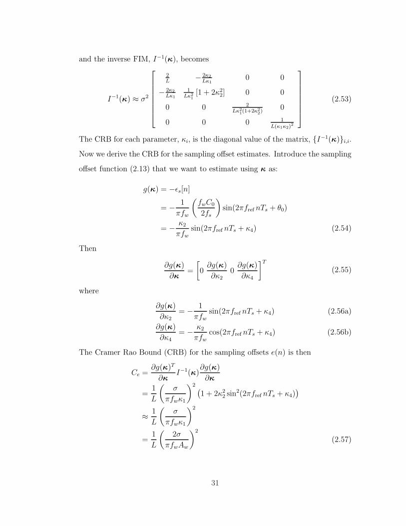
averaged over 300 simulations and the normalized CRB bound.
Figure 2.7 shows the normalized MSE of the estimated sampling offset using
various data lengths L and in the presence of noise. The normalized CRB of the
sampling offset estimation at the 3 different noise powers are the 3 lines in the
plot. As the noise power increases, the CRB increases. From the plot, it can be
seen that the estimation algorithm is performing close to the CRB.
33
2.6 Simulations
The proposed method is tested over a range of input frequencies. The frequency of
the sampling clock, the low-frequency sinusoidal signal, and the high-frequency
sinusoidal signal are set at fs = 1 GHz, fw = 40 MHz and fy = 420 MHz,
respectively. Recall that we assume the high frequency signal y(t) is jittery. We
assume that y(t) from (2.25) is generated using a second-order PLL clock and has
a phase noise. This phase noise can be translated to random jitter τ(t) expressed
in y(t). The phase noise model is described in Appendix 2.B and the parameter
fn in the model is set to 5 MHz. The standard deviation of the random jitter
τ(t) due to phase noise is set to 1% of the sampling period. The frequency of the
reference signal in the PLL feedback loop is fref = 20 MHz. The input signal used
is a sinusoidal tone whose frequency is varied from 25 MHz to 250 MHz in steps
of 25 MHz. To reduce the effects of the training signal on the dynamic range
of the input data, the amplitude of the input signal r(t) and the low-frequency
training signal w(t) are set to 0.8 V and 0.1 V, respectively. In the simulations,
the length L is set to 218, 219, 220. In all the simulations, WGN with standard
deviation σv = 1×10⁻³ is introduced at the input of the ADC and all the results
are averaged over 50 simulation runs. The lowpass filter LPF1 in Figure 2.3 uses
64 taps with passband to 300 MHz and stopband from 350 MHz. The highpass
filter HPF in Figure 2.3 uses 64 taps with stopband up to 300 MHz and passband
from 350 MHz. The lowpass filter LPF2 in the signal extraction block in Figure
2.5 uses 128 taps with a passband up to 70 MHz and stopband from 90 MHz.
2.6.1 Effect of bit resolution
In the first set of simulations, the ADC is assumed to have a 1V peak-to-peak
input range and various bit resolutions 10, 12, 14, 16 are simulated. Figure 2.8
34

and 2.9 show the ratio of the power of the spurious sidebands to the power of
the input tone before and after using the proposed method at 10 bits and 16 bits
ADC resolution, respectively. We denote this ratio as RPSI.
Proposed method with L = 220Proposed method with L = 219Proposed method with L = 218Original spurious sidebands power
Freq [MHz]
RPSI[dB]
50 100 150 200 250−120
−110
−100
−90
−80
−70
−60
Figure 2.8: The plots show the RPSI, ratio of the power of the spurious sidebands (in
the sampled data of a 10 bit ADC) to the power of the input tone, before and after
compensation with σv = 1× 10⁻³.
Proposed method with L = 220Proposed method with L = 219Proposed method with L = 218Original spurious sidebands power
Freq [MHz]50 100 150 200 250
−120
−110
−100
−90
−80
−70
−60
Figure 2.9: The plots show the RPSI in the sampled data of a 16 bit ADC, before and
after compensation with σv = 1× 10⁻³.
35

From the plots, in the original signal, the RPSI varies across frequency. This
can be shown using (2.24) where fw denotes the frequency of the input signal.
When more samples are used to estimate the parameters, the accuracy of the
sampling offset estimates improves. Hence, the spurious sideband suppression
also improves.
To analyze the effect of bit resolution on performance, the next two plots are
generated in the following manner. For each simulated ADC bit resolution, the
average improvement in suppressing the spurious sidebands and the average MSE
of the estimated sampling offset normalized to the power of the sampling offset are
calculated and the results are shown in Figures 2.10 and 2.11, respectively. The
Proposed method with L = 220Proposed method with L = 219Proposed method with L = 218
Bits
RPSIim
provem
ent[dB]
10 11 12 13 14 15 166
8
10
12
14
16
Figure 2.10: The plot shows the trend in suppressing the spurious sidebands using
various bit resolution ADCs.
results show that the sideband suppression performance is directly related to the
accuracy of the sampling offset estimation. The figures also show that when more
data are used, the suppression of the spurious sideband and the sampling offset
estimation improves. In the simulations, WGN with σv = 1× 10⁻³ is fixed while
36

Proposed method with L = 220Proposed method with L = 219Proposed method with L = 218
Bits
Norm
alizedMSE
[dB]
10 11 12 13 14 15 16−20
−18
−16
−14
−12
−10
−8
Figure 2.11: The plot shows the trend in MSE of the estimated sampling offset using
various bit resolution ADCs.
the bit resolution is increased. Increasing bit resolution reduces quantization
noise and there is an improvement from 10 bits to 12 bits. However, when WGN
dominates over quantization noise, the performance is limited when more bits are
used.
We can also compare the MSE performance with the CRB in the previous
section. Recall that in section 2.4.2, we assume the effects of noise from the
noisy high frequency tone is negligible and the signal extraction block output
p[n] only. Subsequently, the performance analysis in the previous section shows
that the estimation error based on p[n] is close to the CRB bound. Here, we
simulate the entire process and evaluate the performance of the estimation error.
When σv = 1 × 10⁻³ and L = 218, 219, 220, we show in Figure 2.11 that the
MSE of the sampling offsets is -10, -13 and -16 dB, respectively. These operating
conditions correspond to σv′ = (1 × 10⁻³)/√2 and L = 218, 219, 220 in Figure
2.7. From the two figures, the MSE values are similar. Therefore, we verifies that
the assumption holds for these simulation parameters.
37

2.6.2 Effect of increasing the amplitude of the training signal
If we increase the amplitude of the training signal, at the expense of reducing
the dynamic range of the input signal, it is possible to improve the parameter
estimation accuracy and, hence, the spur suppression performance. The following
results are generated by fixing L = 218 and using a 10-bit ADC. The amplitude of
the training signal is increased from 0.05 V to 0.25 V, while the amplitude of the
input signal is decreased from 0.85 V to 0.65 V in tandem. The sum of the two
amplitudes remains at 0.9 V. The other simulation parameters remain the same.
Figure 2.12 shows the RPSI as the amplitude of the training signal increases.
Proposed method with Aw = 0.25
Proposed method with Aw = 0.20
Proposed method with Aw = 0.15
Proposed method with Aw = 0.10
Proposed method with Aw = 0.05
Original spurious sidebands power
Freq [MHz]
RPSI[dB]
50 100 150 200 250−130
−120
−110
−100
−90
−80
−70
−60
Figure 2.12: The same simulation parameters as in Fig. 2.8 are used, except that L is
fixed at 218 and the amplitudes of the training and input signals are varied.
To examine the improvement in spur suppression against the amplitude of
the training signal, the next plot is shown. Figure 2.13 shows the average spur
suppression improvement as the amplitude of the training signal is increased from
0.05 V to 0.25 V. We see that doubling the amplitude of the training signal from
0.1 V to 0.2 V reduces the spurious tones from 9 dB to 14 dB. If we compare this
38

against Figure 2.10, the same amount of improvement is obtained when the data
length L is quadrupled (with a 10 bit ADC). This can also be inferred from the
CRB bound (2.57) where it is inversely proportional to the data length L and
the square of the amplitude of the training signal κ1.
Amplitude of training signal [V]
RPSIim
provem
ent[dB]
0.05 0.1 0.15 0.2 0.252
4
6
8
10
12
14
16
Figure 2.13: The plot shows the trend in suppressing the spurious sidebands as the
amplitude of the training signal increases.
2.6.3 Effect of additional random jitter in ADC
In the proposed architecture (Figure 2.3), other sources of imperfection may be
present. One source of imperfection is that the sampling clock itself may have
random jitter in addition to the deterministic sideband distortion caused by the
PLL and which we examined in this paper. Another possible error is that the
low-frequency training signal w(t) may have some amount of random jitter as
well. As such, we included these imperfections into the simulations with a 10 bit
ADC. In the next set of simulations, random time jitter based on a second-order
PLL model is generated. The phase noise model is described in Appendix 2.B.
39

In the phase noise model, fn is set to 5MHz and the standard deviation of the
random jitter is normalized to the sampling interval. We denote the standard
deviation of the jitter in the ADC and w(t) by σADC and σLF , respectively. We
choose σADC and σLF , expressed as percentages of the sampling period, from
the set 0.1, 0.5, 1, 5, 10%. We first investigate the effects when random jitter is
present in the ADC.
The left-sided plots in Figure 2.14 and 2.15 show the PSD where a tone at
125 MHz is perturbed by both the spurious sideband and random jitter (σADC at
0.5% and 1%) in the ADC. Notice that as σADC is increased, the random jitter
Sidebands
Recovered Signal
Freq [MHz]
Sidebands
Original Signal
dB
Freq [MHz]100 120 140 160100 120 140 160
−120
−100
−80
−60
−40
−20
0
−120
−100
−80
−60
−40
−20
0
Figure 2.14: The plots show the PSD of a tone at 125 MHz before and after signal
recovery, when the random jitter σADC in the ADC is 0.5%.
creates a noisy spectrum around the tone. The right-sided plots in the figures
show the PSD of the recovered signal.
Figure 2.16 shows the ratio of the power of the spurious sidebands in the
sampled data to the power of the input signal in the presence of the random
jitter in the ADC. The parameters used are the same as those used in Figure 2.8
except that random jitter (σADC at 1% of the sampling period) in the ADC is
added.
40

Sidebands
Recovered Signal
Freq [MHz]
Sidebands
Original Signal
dB
Freq [MHz]100 120 140 160100 120 140 160
−120
−100
−80
−60
−40
−20
0
−120
−100
−80
−60
−40
−20
0
Figure 2.15: The plots show the PSD of a tone at 125 MHz before and after signal
recovery, when the random jitter σADC in the ADC is 1%.
Figure 2.17 is used to analyze the performance when the power of the ran-
dom jitter in the ADC is changed. The plot shows the average improvement in
the sideband suppression when σADC is varied. From the plot, the performance
degrades when σADC increases above 1%.
2.6.4 Effect of noise in training signal
The simulations are repeated again except that the training signal has some
random jitter due to imperfections. Figure 2.18 shows the average improvement
in the sideband suppression when σLF is varied. From the plot, the algorithm
performs well when σLF is below 1% and degrades when it is increased beyond
1%.
2.7 Conclusion
In this chapeter we modeled the effect of PLL imperfections on sampled data
and proposed a technique to compensate for the presence of the spurious tones.
41

Proposed method with L = 220Proposed method with L = 219Proposed method with L = 218Original spurious sidebands power
Freq [MHz]
RPSI[dB]
50 100 150 200 250−120
−110
−100
−90
−80
−70
−60
Figure 2.16: The plot is generated using the same parameters as in Figure 2.8 except
that random jitter (σADC = 1%) in the 10-bit ADC is included.
A training signal is used to estimate the distortion and a filter implementation
is used to remove the distortions from the sampled data by using discrete-time
processing techniques. Simulation results verify that the proposed method is
effective under Gaussian noise, quantization noise, random jitter in the ADC,
and random jitter in the training signal itself.
2.A Derivation of relative error bounds
In this appendix, we derive the relative error bound between the actual e[n] and
its approximation in (2.13). Let xn refer to the approximate value (i.e.,−ǫs[n])for the true value xn (i.e., e[n] = −ǫs(tn)). To find how close xn is to xn, we call
upon Taylor’s theorem [44].
Suppose h is a real function on [a, b], m is a positive integer, the (m − 1)-th
derivative h(m−1)(t) is continuous on [a, b] and h(m)(t) exists for every t ∈ (a, b).
42

Proposed method with L = 220Proposed method with L = 219Proposed method with L = 218
σADC
RPSIim
provem
ent[dB]
10−1 100 101−15
−10
−5
0
5
10
15
Figure 2.17: The plot shows the trend in suppressing the spurious sidebands using the
same parameters in Fig. 2.10 with a fixed 10 bit ADC and varying the ADC jitter
σADC (as a percentage to the sampling period).
Proposed method with L = 220Proposed method with L = 219Proposed method with L = 218
σLF
RPSIim
provem
ent[dB]
10−1 100 101−2
0
2
4
6
8
10
12
14
Figure 2.18: The plot uses the same parameters as in Fig. 2.17, except that σADC = 0
and σLF is varied.
Let α, β be distinct points in [a, b], and define
P (t) , h(α) +
m−1∑
k=1
h(k)(α)
k!(t− α)k (2.58)
43

Then Taylor’s theorem states that there exists a point ξ between α and β such
that
h(β) = P (β) +h(m)(ξ)
m!(β − α)m (2.59)
with exact equality in (2.59). The theorem shows that h(t) can be approximated
by P (t) (a polynomial of degree m−1) and (2.59) allows us to estimate the error
if we know bounds on |h(m)(ξ)|.
First, we define a function gn(x) as
gn(x) , x+ ǫs(nTs + x) (2.60)
where the root of gn(x) is at xn = e[n]. Also note that xn = −gn(0). Using
Taylor’s theorem and setting m = 1, α = 0, β = x and 0 ≤ ξ ≤ x, we use (2.59)
to express gn(x) in (2.60) exactly as:
gn(x) = gn(0) + gn(ξ) x (2.61)
where
gn(x) = 1 + γ cos(2πfref(nTs + x) + θ0) (2.62a)
γ , C0freffs, 0 < γ < 1 (2.62b)
The condition γ = C0fref/fs < 1 is assumed to hold since the frequency, fref, of
the reference signal and C0 in a typical PLL system are small compared to the
frequency, fs, of the clock signal. Let xn, ξn be the solution to gn(xn) = 0.
Then (2.61) gives
xn = − gn(0)
gn(ξn)= e[n] (2.63)
From (2.62), the term gn(ξn) can be bounded as
0 ≤ 1− γ ≤ gn(ξn) ≤ 1 + γ (2.64)
44

Therefore, if gn(0) < 0 then xn is bounded by
−gn(0)1 + γ
≤ xn ≤ −gn(0)1− γ
(2.65)
If instead gn(0) > 0, the lower and upper bounds on xn are reversed. Now observe
from (2.60) that xn is
xn = −ǫs[n]
= −gn(0)(2.66)
Therefore,
gn(0)(
−γ
1−γ
)
≤ xn − xn ≤ gn(0)(
γ
1+γ
)
, when gn(0) > 0
gn(0)(
γ
1+γ
)
≤ xn − xn ≤ gn(0)(
−γ
1−γ
)
, when gn(0) < 0(2.67)
The absolute error is bounded by
|xn − xn| ≤ |gn(0)|γ
1− γ(2.68)
From (2.63), if gn(0) 6= 0 then xn 6= 0. Therefore, we could use (2.63) and (2.68)
to express the relative error as
∣∣∣∣
xn − xnxn
∣∣∣∣≤ |gn(ξn)|
γ
1− γ(2.69)
Using (2.62) we note that |gn(ξn)| ≤ 1 + γ. We conclude that the relative error
is bounded by
∣∣∣∣
xn − xnxn
∣∣∣∣≤ γ(1 + γ)
1− γ(2.70)
2.B Modeling of phase noise in second-order PLL
This appendix describes the phase noise model used in the simulations for the
random jitter in the high frequency jittery tone fy(t), and when additional ran-
dom jitter is introduced into the ADC and training signal. From [9, 22], the
45

closed-loop transfer function for a second-order PLL is
H(s) =2ηωns+ ω2
n
s2 + 2ηωns+ ω2n
(2.71)
where ωn is the loop natural frequency and η is the damping factor. If we let
η = 1√2, then the single-sided PSD of the phase noise model for the second-order
PLL can be shown to be
Sφ(f) = |1−H(j2πf)|2 ν
πf 2
=νf 2
π(f 4 + f 4n)
(2.72)
where fn = ωn
2πis a measure of the loop bandwidth and ν is called the oscillator
linewidth. The variance is ν
2√2fn
and the autocorrelation function of the phase
noise φ(t) is
Rφ(λ) =
∫ ∞
−∞
νf 2
2π(f 4 + f 4n)ej2πfλdf (2.73)
Using the PSD and autocorrelation model, it is possible to simulate the phase
noise in a second-order PLL. We can relate the phase noise to the time jitter in
a clock signal with frequency fs as φ(t) = 2πfsτ(t). The standard deviation of
the random jitter is 12πfs
σφ. Normalizing the standard deviation to the sampling
interval yields στ = 12πσφ.
2.C Effect of jitter in y(n) on training signal extraction
Based on the simulation parameters in section 2.6, we fix the standard deviation
of the jitter in y(t) to be 1% of the sampling period. Equivalently, this means
that the standard deviation of the phase noise is 1% of 2π. From Appendix 2.B,
the variance of the phase noise is ν
2√2fn
. In this work, fn is set to 5 MHz. Hence,
ν is 5.58× 10⁴ Hz.
46

In section 2.4.2, we like to retain the low-frequency signal w(n) (as shown in
Figure 2.4). The highest frequency component of w(n) is at 60 MHz. Also, we
we see that the closest jitter’s spectrum is the one that is centered at 120 MHz.
The offset between the two frequencies is 60 MHz. Using (2.28) in section 2.4.2
and (2.72) in Appendix 2.B, the noise power from the jitter onto the highest
frequency component of w(n) is
A2wf
2yB
16f 2s
Sφ(fd) (2.74)
where fd is the offset frequency, B is the frequency resolution of the PSD. Using
the parameters in the simulations, Aw = 0.1 V, fy = 420 MHz, fs = 1 GHz and
B ≈ 1 KHz, the noise power at 60 MHz is -122 dB.
2.D Phase estimation
This appendix describes a way to estimate the phases in the tones in (2.30), which
are used in the phase recovery of the signal extraction block diagram in Figure
2.5. To estimate the phase of a sinusoid at frequency fk in a signal of the form
s[n] =
K∑
k=0
Ak cos(2πfknTs + θk) (2.75)
we collect N samples and calculate the following expressions:
wma =1
N
N−1∑
n=0
s[n] cos(2πfknTs) (2.76a)
wmb =1
N
N−1∑
n=0
s[n] sin(2πfknTs) (2.76b)
47

Substituting (2.75) into (2.76) gives:
wma =1
N
N−1∑
n=0
s[n] cos(2πfknTs)
=1
N
N−1∑
n=0
K∑
ℓ=0
Aℓ cos(2πfℓnTs + θk) cos(2πfknTs)
=1
N
N−1∑
n=0
K∑
ℓ=0
Aℓ
2[cos(2π(fℓ + fk)nTs + θk) + cos(2π(fℓ − fk)nTs + θk)]
=1
N
N−1∑
n=0
Ak
2cos(θk) +
K∑
ℓ=0
1
N
N−1∑
n=0
Aℓ
2cos(2π(fℓ + fk)nTs + θk)
+K∑
ℓ=0,ℓ 6=k
1
N
N−1∑
n=0
Aℓ
2cos(2π(fℓ − fk)nTs + θk)
≈ Ak
2cos(θk) (2.77)
and
wmb =1
N
N−1∑
n=0
s[n] sin(2πfknTs)
=1
N
N−1∑
n=0
K∑
ℓ=0
Aℓ cos(2πfℓnTs + θk) sin(2πfknTs)
=1
N
N−1∑
n=0
K∑
ℓ=0
Aℓ
2[sin(2π(fℓ + fk)nTs + θk)− sin(2π(fℓ − fk)nTs + θk)]
= − 1
N
N−1∑
n=0
Ak
2sin(θk) +
K∑
ℓ=0
1
N
N−1∑
n=0
Aℓ
2sin(2π(fℓ + fk)nTs + θk)
−K∑
ℓ=0,ℓ 6=k
1
N
N−1∑
n=0
Aℓ
2sin(2π(fℓ − fk)nTs + θk)
≈ −Ak
2sin(θk) (2.78)
Then we estimate the phases θk using
θk = − tan−1
(wmb
wma
)
(2.79)
48

CHAPTER 3
Compensating Spurious PLL Tones in Spectrum
Sensing Architectures
In the previous chapter, we showed that spurious tones in the sampling clock
creates spurious tones in the sampled data of the ADCs. In applications like
spectrum sensing in cognitive radios, spurious tones might give a false positive
detection on actual free channels. To share the frequency spectrum effectively
(such as unused TV bands) there is a need to design better receivers that can
reliably sense free spectrum holes even in the presence of spurious tones [45–47],
especially since cognitive radios are expected to be able to detect very weak sig-
nals [46, 48]. There are various methods that have been used in the literature
to detect such signals, including, energy detection methods, matched filtering
methods and feature detection methods [46, 48, 49]. Moreover, for wideband ap-
plications, it is common to split the spectrum into smaller channels for detection.
For example, references [50, 51] use fast Fourier transform (FFT) to channelize
the spectrum before energy detection. Alternative ways to channelize the spec-
trum also exist [52–54]. Reference [52] proposed a method to sense the channels
serially using a reconfigurable downconverter and filter. Reference [53] proposed a
low-power multiresolution spectrum sensing IC which uses energy detection. Ref-
erence [54] proposed and analyzed a two-stage sensing technique that performs
a coarse resolution sensing (CRS) followed by a fine resolution sensing (FRS).
49

The CRS and FRS are performed using a random search and a sequential search,
respectively. In these techniques, it is assumed that an ideal clock is used in
the ADC [50, 51], or in the DDC reference frequency generator [52], or in the
mixer [53]. Here, we show that when the spurious tones in the non-ideal clock
of the ADC are not considered, the false alarm rate will increase. Even if the
difficulty caused by the spurious tones is considered and the thresholds are raised
to reduce the false alarm, the resulting detection rates are likely to decrease.
For these reasons, it is desirable to seek an alternative approach to remove the
spurious sidebands from the sampled data and improve the sensing performance.
In this chapter, we extend the work in the previous chapter from using a si-
nusoidal reference signal to using a general periodic reference signal, and propose
a new approach [18, 55] that relies specifically on the use of a Fourier transform
block (since it is a common building block in wideband applications such as spec-
trum sensing). By reusing existing components, we aim to reduce the hardware
complexity and computation cost when estimating the distortions. The work here
proposes a modification to a spectrum sensing architecture by first performing off-
set estimation on a training sinusoidal signal and then switching to compensating
the distorted samples to obtain the dejittered samples for spectrum sensing. The
offset estimation algorithm (using the training signal and the Fourier transform),
and the compensation algorithm (using first-order Taylor series) are called the
TFT and FOT, respectively. We provide detailed derivations of the distortion
sampling offsets, show that replicas of the modulated signals are created when
the modulated signals are sampled non-uniformly with the derived offsets, evalu-
ate the impact of this distortion during spectrum sensing, derive the theoretical
detection performance for some signals, and simulate to verify the detection per-
formance before and after using the proposed algorithm. To evaluate the effects
on detection performance, we consider the case when the signal of interest is a
50

weak signal. We also assume that there is a strong signal at some frequency
offset from the signal of interest. The distortions to the sampled data create
spurious sidebands from the strong signal and we assume that the spurious side-
bands overlap with the signal of interest. Hence, the spurious sidebands become
an interference to the detection of the weak signals.
The chapter is organized as follows. Section 3.1 discusses a mathematical
model for a VCO clock and what happens when the reference signal is leaked
into the control line of the VCO. It also shows the effect on sampling instants
and the sampled data when the sampling clock is used with an ADC. Section
3.2 proposes the TFT that estimates the sidebands of the sampled data using
a Fourier transform block, and the FOT that compensates for the distortions.
Section 3.3 considers the detection performance using an energy detector in the
presence of the spurious sidebands distortion. Section 3.4 presents the simulation
results and Section 3.5 summarizes the chapter.
3.1 Effects of leakage from reference signal
3.1.1 Reference leakage in PLL
In [22, 37], a voltage-controlled oscillator (VCO) is described as a circuit that
generates a periodic clock signal, s(t), whose frequency is a linear function of a
control voltage, Vcont. Let the gain of the VCO and its “free running” frequency
be denoted by Kvco and fs, respectively. The generated clock signal is described
by
s(t) = As sin
(
2πfst +Kvco
∫ t
−∞Vcontdt
)
(3.1)
To attain some desired oscillation frequency, Vcont is set to some constant value.
However, the generated signal, s(t), may not be an accurate tone. To attain good
51

frequency synthesis, a frequency-divided version of the clock signal is fed into a
block that consists of a PFD, a CP and a low-pass filter (LPF) as shown in Fig.
3.1. The PFD/CP/LPF block compares the frequency-divided clock signal with
Figure 3.1: Block diagram of a PLL.
a low-frequency reference signal at fref and makes adjustments to Vcont. The low-
frequency reference signal can be generated using a low-frequency oscillator (e.g.,
a crystal oscillator). Due to imperfections in the circuitry, the reference signal
leaks into the control line of the VCO. Also note that the presence of the LPF
attenuates the leakage signal but fails to remove it completely. For simplicity, we
assume that the desired clock signal at fs is obtained when Vcont is 0. The refer-
ence leakage is assumed to be some periodic signal with fundamental frequency
fref [40]. From [40], one source of reference leakage in the PFD/CP/LPF block
is due to the current mismatch in the CP. The current mismatch creates rect-
angular pulses which are passed through the LPF. Hence, the higher frequencies
components are attenuated and the leakage waveform changes (depending on the
LPF’s frequency response). Another source of leakage is from the reference signal
and the PFD. Similarly, the leakage waveform is also changed due to the LPF.
In this paper, we do not need to know the exact waveform except that it is a
periodic signal. For illustration purposes, we assume here that the periodic signal
is a triangular waveform and can be described by its Fourier series representation.
First, note that the Fourier series representation of a triangular waveform with
52

peak amplitude of 1 and a fundamental frequency of fref is given by:
Vr(t) =8
π2
∞∑
k=0
(−1)k
(2k + 1)2sin((2k + 1)2πfreft)
=8
π2
∞∑
k=0
(−1)k
(2k + 1)2cos((2k + 1)2πfreft−
π
2) (3.2)
Now, suppose there is leakage into the control line so that Vcont becomes a delayed
and scaled version of Vr(t), say,
Vcont =
∞∑
k=0
Vk cos (2πfkt + θk) (3.3)
where
θk = 2πfref(2k + 1)τ − π
2(3.4a)
Vk = V0(−1)k
(2k + 1)2(3.4b)
fk = (2k + 1)fref (3.4c)
for some V0, τ.
3.1.2 Effect of leakage on the sampling clock of the ADC
Then, using (3.1), the output of the VCO becomes
s(t) = As sin (2πfst + ǫs(t) + φs) (3.5)
where φs is some unknown phase offset and
ǫs(t) =∞∑
k=0
Ck sin (2πfkt+ θk) (3.6)
and
Ck =Kvco
2πfkVk (3.7)
53
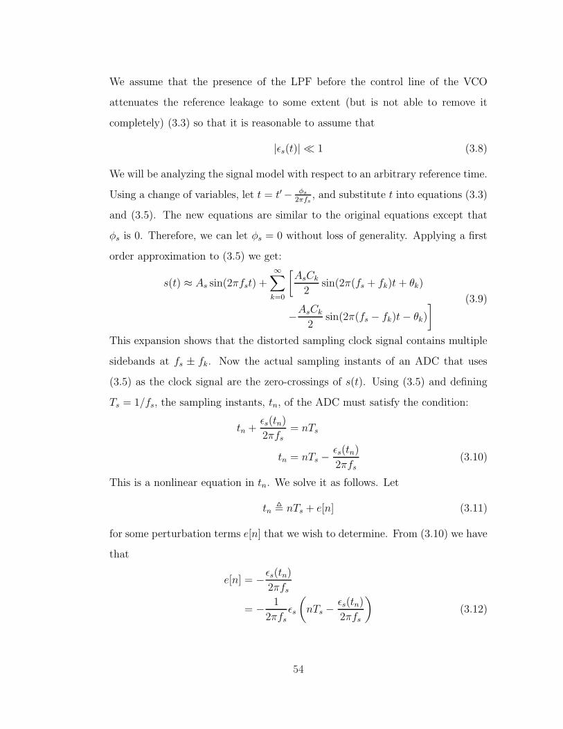
We assume that the presence of the LPF before the control line of the VCO
attenuates the reference leakage to some extent (but is not able to remove it
completely) (3.3) so that it is reasonable to assume that
|ǫs(t)| ≪ 1 (3.8)
We will be analyzing the signal model with respect to an arbitrary reference time.
Using a change of variables, let t = t′− φs
2πfs, and substitute t into equations (3.3)
and (3.5). The new equations are similar to the original equations except that
φs is 0. Therefore, we can let φs = 0 without loss of generality. Applying a first
order approximation to (3.5) we get:
s(t) ≈ As sin(2πfst) +∞∑
k=0
[AsCk
2sin(2π(fs + fk)t + θk)
−AsCk
2sin(2π(fs − fk)t− θk)
] (3.9)
This expansion shows that the distorted sampling clock signal contains multiple
sidebands at fs ± fk. Now the actual sampling instants of an ADC that uses
(3.5) as the clock signal are the zero-crossings of s(t). Using (3.5) and defining
Ts = 1/fs, the sampling instants, tn, of the ADC must satisfy the condition:
tn +ǫs(tn)
2πfs= nTs
tn = nTs −ǫs(tn)
2πfs(3.10)
This is a nonlinear equation in tn. We solve it as follows. Let
tn , nTs + e[n] (3.11)
for some perturbation terms e[n] that we wish to determine. From (3.10) we have
that
e[n] = −ǫs(tn)2πfs
= − 1
2πfsǫs
(
nTs −ǫs(tn)
2πfs
)
(3.12)
54

Since |ǫs(t)| ≪ 1,∣∣∣∣
ǫs(tn)
2πfs
∣∣∣∣≪ Ts (3.13)
Therefore, the discrete sequence of offsets e[n] is approximated as
e[n] ≈ −ǫs[n]2πfs
(3.14)
3.1.3 Effect of distorted sampling offsets on training signal
Let us now analyze the effect of this distorted sampling on a pure sinusoidal
training tone at the input of the ADC. Since the frequency of the training signal
is much lower than the frequency of the sampling clock generated by the PLL, it
is reasonable to assume that a low frequency oscillator (e.g., a crystal oscillator)
can be used to accurately generate the signal. As such, we assume that the
training signal does not have the same distortion problems as the sampling clock.
Let the input signal to the ADC be
w(t) = Aw cos(2πfwt + φw) (3.15)
Then the sampled signal, w[n], is approximated as
w[n] ≈ w (nTs + e[n])
≈ w[n] + e[n] w[n](3.16)
where
w[n] = w(t)|t=nts
w[n] = w(t)|t=nts (3.17)
Using trigonometry expansions, the term e[n] w[n] in (3.16) is
e[n]w[n] =
∞∑
k=0
fwAwCk
2fs[cos(2π(fw − fk)nTs + φw − θk)
− cos(2π(fw + fk)nTs + φw + θk)]
(3.18)
55

The above expression shows that the sampled data consists of the input signal
and multiple frequency components at fw ± fk. If the magnitude of the Fourier
series coefficients of the reference signal in the PLL decreases rapidly, then the
higher frequencies components in (3.14) and (3.18) can be ignored. Observe that
the amplitude term in (3.18) is directly proportional to the fw. This means that
the power of the spurious sidebands increases with the frequency of the input
signal.
It is possible to relate the power of the sidebands in the sampled data (3.18)
to the sidebands in the sampling clock (3.9). For example, suppose the power
ratio of the sideband at fs+f0 of the clock, s(t), to the tone at fs is -50 dBc, then
C0 is 6.32×10⁻³. Thus, the power of the sideband at fw+f0 of the sampled data
can be derived. As an example, the reference leakage in the PLL is simulated as
a triangular wave with a fundamental frequency of 20 MHz and is approximated
using the first 4 Fourier series coefficients. A sinusoidal training signal at 45
MHz is distorted by the jittered sampling and its power spectral density (PSD)
is shown in Fig. 3.2. From the plot, only the sidebands at 25 MHz, 65 MHz and
105 MHz are detected (i.e., the effects from the first 2 Fourier series coefficients).
dB
Freq [MHz]
Sidebands
0 50 100 150 200 250−120
−100
−80
−60
−40
−20
0
Figure 3.2: The plot shows the PSD of the distorted training signal with two sidebands.
56

3.1.4 Effects of the spurious sidebands on spectrum sensing
The previous section shows that the ADC creates spurious tones in the sampled
data. These tones are not supposed to exist and can lead to false alarm in
wideband spectrum sensing applications. Moreover, we can further show that
when the input signal is a modulated signal, then the distorted samples create
replicas of the modulated signal at some offset frequencies. Specifically, suppose
now that w(t) is a modulated signal of the form:
w(t) = m(t) cos(2πfwt+ φw) (3.19)
where m(t) is the message signal and fw is the carrier frequency. Differentiating
w(t) gives
w(t) = m(t) cos(2πfwt+ φw)− 2πfwm(t) sin(2πfwt+ φw)
≈ −2πfwm(t) sin(2πfwt + φw)(3.20)
The first term in the first line of (3.20) is removed because we assume that m(t)
is a bandlimited baseband signal, whose frequency components are much smaller
than the carrier frequency fw. As such, we assume that m(t) is small relative to
2πfwm(t). Consequently, the distorted samples become
w[n] ≈ w[n] + e[n] w[n]
= m[n] cos(2πfwnTs + φw) + e[n] w[n](3.21)
where the sidebands are in the second term:
e[n]w[n] =∞∑
k=0
fwCk
2fsm[n][cos(2π(fw − fk)nTs + φw − θk)
− cos(2π(fw + fk)nTs + φw + θk)]
(3.22)
The above expressions, as indicated earlier, show that the spurious sidebands
are replicas of the original modulated signal at a lower amplitude and frequency-
shifted by fk.
57

3.2 Proposed solution
In a typical spectrum sensing application, there is usually a module that performs
Short-Time Fourier Transform (STFT) with windowing functions. To save com-
putation and hardware complexity, we will use this module as a building block in
our proposed solution. Figure 3.3 shows the proposed architecture. We assume
Figure 3.3: Proposed architecture for reducing the effects of PLL sidebands in spectrum
sensing applications.
that the PLL is in tracking mode (when the loop is in lock) and the distortions to
the sampled data due to the PLL sidebands can be estimated from a sinusoidal
training tone w(t). The distorted sampled data w[n] are used with the STFT
module to estimate the sampling distortions (using the TFT algorithm). Once
the distortions (3.14) are estimated, the circuit switches and starts sampling the
desired input signal and the sampled data is corrected in the digital domain before
the spectrum sensing application (using the FOT algorithm).
3.2.1 TFT algorithm
We can use the results in (3.18) to evaluate the sampling offsets’ parameters
Ck, θk in (3.14) from the sidebands present in w[n]. First, we express (3.15) as
w[n] = Aw cos(2πfwnTs + φw) (3.23)
58

Let us assume we have estimated the amplitude and phase of the tones in (3.18).
We will show how to estimate them further ahead (see (3.31)). Let Z(f) = Aejθ
denote the complex representation of the estimated amplitude A and phase θ at
frequency f . Let ∗ denote complex conjugation. Then, using (3.23) and (3.18),
Ck, θk can be estimated from the relation
Ckejθk =
2fse−jπ
fw
(Z(fw + fk)
Z(fw)
)
=2fse
−jπ
fw
(Z(fw + fk)Z
∗(fw)
|Z(fw)|2) (3.24)
or,
Ckejθk =
2fsfw
(Z∗(fw − fk)
Z∗(fw)
)
=2fsfw
(Z∗(fw − fk)Z(fw)
|Z(fw)|2) (3.25)
The question now is how to estimate the sinusoidal sidebands to enable evaluation
of Ck, θk through (3.24) or (3.25). As mentioned before, in spectrum sensing
applications, there is a module that performs STFT with windowing. Essentially,
this module splits the data into different frequency bins for further processing.
The operation of the STFT is as follows [56].
In the m-th iteration of STFT, an N -point Fast Fourier Transform (N -FFT)
is applied on an N -point data sequence with a windowing function wx[n]. Let us
assume that data sequences do not overlap and let us denote the data sequences
by x[n +Nm]. Thus, the STFT output is
X [m, k] =
N−1∑
n=0
wx[n]x[n +Nm]e−j2π kNn (3.26)
where k is a particular frequency bin in the N -FFT. Suppose we want to estimate
59

the amplitude and phase of a sinusoid at frequency fp in a signal of the form:
x[n] =
P∑
i=0
Ai cos(2πfinTs + θi)
=P∑
i=0
Ai
2
[ej(2πfiTsn+θp) + e−j(2πfiTsn+θp)
]
(3.27)
and only the sinusoid lies in the p-th frequency bin, then the STFT output of the
bin is
X [m, p] = Xp[m, p] +Xn[m, p] (3.28)
where
Xp[m, p] = Ap
[ape
j(2πfpTsNm+θp) + bpe−j(2πfpTsNm+θp)
](3.29a)
ap =1
2
N−1∑
n=0
wx[n]ej2π(fpTs− p
N)n (3.29b)
bp =1
2
N−1∑
n=0
wx[n]e−j2π(fpTs+
pN)n (3.29c)
TheXn[m, p] are nuisance terms involving the rest of the frequency components in
x[n] that are out of the p-th frequency band of the FFT. Using proper windowing
functions wx[n], we can attenuate the effect of Xn[m, p]. As an example, a STFT
using 1024-pt FFT is applied on the training signal shown in Fig. 3.2. The
STFT output in the frequency bin that contains the sideband tone at 65MHz is
extracted and its frequency spectrum is plotted in Fig. 3.4. The left and right
plots show the result when no windowing is used, i.e., wx[n] = 1 and when a
Blackman-Harris window is used, respectively. As shown, the window function
reduces the spectral leakage of out-of-band signals into the frequency channel.
60

Freq [MHz]
Desired Sideband
dB
Freq [MHz]
Desired Sideband
64.7 64.8 64.9 65 65.164.7 64.8 64.9 65 65.1−140
−120
−100
−80
−60
−40
−140
−120
−100
−80
−60
−40
Figure 3.4: The plots show the frequency domain output of a frequency channel in the
STFT when no windowing is used (left) and windowing is used (right).
Thus, manipulating X(m, p) yields
dp[m] ,1
|ap|2 − |bp|2[
a∗p −bp]
X [m, p]
X [m, p]∗
= Apejθpej2πfpTsNm + ν[m]
= Z(fp)ej2πfpTsNm + ν[m]
(3.30)
where ν[m] is some noise residual in terms of Xn[m, p]. Thus, we can estimate
Z(fp) from the data dp[m] using M samples.
Z(fp) =1
M
M−1∑
m=0
dp[m]e−j2πfpTsNm (3.31)
The TFT algorithm is summarized in Algorithm 3.1.
3.2.2 Block diagram of TFT
The TFT algorithm described in the previous section can be converted to a block
diagram as shown in Fig. 3.5. First, let us assume that we are interested in
suppressing the spurious sidebands at f0 and f1 away from the training signal’s
frequency (fw). The data w[n] is segmented into blocks of size N before it is
61

Algorithm 3.1 Summary of TFT algorithm
Require: Denote the frequency of the training signal as fp0 = fw and the frequency
of the sidebands as fpk = fw + fk−1, k = 1, · · · ,K. Also, denote the STFT
channels that the training signal and sidebands lie in as p0 and pk, k = 1, · · · ,K,
respectively. Finally, precompute apk and bpk, k = 0, · · · ,K, from (3.29).
for m = 0, · · · ,M − 1 do
for k = 0, · · · ,K do
dpk[m] =1
|apk|2 − |bpk|2[
a∗pk −bpk
]
X[m, pk]
X[m, pk]∗
end for
end for
for k = 0, · · · ,K do
Z(fpk) =1
M
M−1∑
m=0
dpk[m]e−j2πfpkTsNm
end for
for k = 1, · · · ,K do
Ck−1ejθk−1 =
2fse−jπ
fw
(
Z(fpk)
Z(fw)
)
end for
ǫs[n] =
K−1∑
k=0
Ck sin(
2πnfkTs + θk
)
e[n] = − ǫs[n]
2πfs
62

Figure 3.5: Block diagram of the TFT algorithm. The STFT, Apk and Bfk blocks
represent the different stages of the proposed algorithm and their block diagrams are
shown in Fig. 3.6, Fig. 3.7 and Fig. 3.8, respectively. Firstly, the STFT block
channelizes the training signal w[n]. Then, the parameters of the sidebands in selected
channels (pk) are estimated using the Apk blocks. Finally, the Bfk blocks generate
some data streams which are added together to obtain the estimated sampling offsets
e[n].
processed by the existing STFT block. The input to the STFT is x[n] = w[n].
The STFT block performs the windowed FFT and outputs X [m, k] for the mth
channel (step 1 of TFT algorithm). The detailed block diagram of STFT is shown
in Fig. 3.6. We denote multiplication with fixed constant by a triangular symbol.
We also assume that X [m, p0], X [m, p1] and X [m, p2], contain the training signal
at fw and its spurious sidebands at fw + f0 and fw + f1, respectively.
Figure 3.6: Block diagram of STFT.
In the next stage (Apk blocks) of Fig. 3.5, the phase and amplitude of the tone
in each of the STFT channels X [m, p0], X [m, p1] and X [m, p2] are estimated as
63
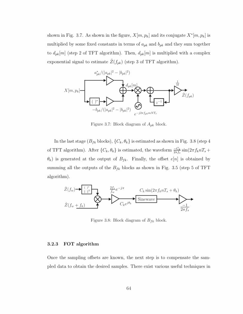
shown in Fig. 3.7. As shown in the figure, X [m, pk] and its conjugate X∗[m, pk] is
multiplied by some fixed constants in terms of apk and bpk and they sum together
to dpk[m] (step 2 of TFT algorithm). Then, dpk[m] is multiplied with a complex
exponential signal to estimate Z(fpk) (step 3 of TFT algorithm).
Figure 3.7: Block diagram of Apk block.
In the last stage (Bfk blocks), Ck, θk is estimated as shown in Fig. 3.8 (step 4
of TFT algorithm). After Ck, θk is estimated, the waveform −Ck
2πfssin(2πfknTs+
θk) is generated at the output of Bfk. Finally, the offset e[n] is obtained by
summing all the outputs of the Bfk blocks as shown in Fig. 3.5 (step 5 of TFT
algorithm).
Figure 3.8: Block diagram of Bfk block.
3.2.3 FOT algorithm
Once the sampling offsets are known, the next step is to compensate the sam-
pled data to obtain the desired samples. There exist various useful techniques in
64
the literature [57–59] that reconstruct signals from non-uniformly sampled data.
For example, [57] proposed a technique based on Taylor series and derived a
differentiator-multiplier cascade (DMC) system to reconstruct signals using up
to the third order of the Taylor series. Reference [58] proposed a method based
on Lagrange interpolation and modified it for band-limited signals. This modi-
fied Lagrange interpolator is called the functionally weighted (FW) interpolator.
Reference [59] described the barycentric interpolator and showed that the FW
interpolator in [58] can be converted to a barycentric interpolator. Reference [59]
states that the reconstruction performance of the algorithms in [58] and [59] is
similar. The algorithms in [57–59] are able to handle large sampling offsets. For
example, [58, 59] can handle sampling offsets up to half of the sampling period.
In this work, we use a similar method as our previous works [17, 36, 41, 55]
to dejitter the sampled data. The method is motivated using a first-order Tay-
lor series and it is denoted as FOT. As such, it is the same as stage 1 of the
DMC in [57]. We have also evaluated the performance if we use the techniques
from [57, 58]. We do not compare with the barycentric interpolator from [59]
since the performance is similar to the FW interpolator from [58]. We found
that under the simulation settings used in this work, when the distortion sam-
pling offsets are small (0.1% of the sampling period), no significant improvement
is provided by these other methods. However, when the size of the distortion
sampling offsets is increased, the techniques in [57–59] can be useful albeit at
higher computational complexity. The details of the comparison are described in
Appendix 3.B. Therefore, our proposed technique is able to compensate for the
effect of small sampling distortions using an efficient architecture that exploits
the convenience of the FFT operation.
65

The desired data, r[n], can be expressed as:
r[n] , r(nTs)
= r (nTs + e[n]− e[n])
≈ r(nTs + e[n])− e[n]r(nTs + e[n])
= r[n]− e[n]r(nTs + e[n]) (3.32)
where r[n] are the distorted samples, e[n] are the estimated sampling errors (see
(3.14)), and r(nTs + e[n]) are the derivatives of r(t) at t = nTs + e[n]. A block
diagram showing the FOT algorithm is illustrated in Fig. 3.9. The derivatives
can be approximated using a discrete filter applied to r[n]. The ideal frequency
response of a derivative is a slope (see Fig. 3.10). Here, we like to compensate
the input signal up to 200 MHz (or 0.8π rad/sample). Therefore, we designed a
15-tap filter where we minimized the frequency response error (from 0 to 0.8π)
using a norm-1 criterion. The frequency response of the 15-tap filter is shown in
Fig. 3.10.
-
+
r[n]
e[n]
derivative
filter
de-jittered
samples r[n]
Figure 3.9: Block diagram of the FOT algorithm.
3.3 Detection of signals using an energy detector
In spectrum sensing, one way to detect signals at different frequencies is to use a
STFT to channelize the wideband spectrum and to detect the presence of signals
in each of the channels [49, 50].
66

ideal derivative filter
15-tap derivative filter
radians per sample
0 0.2π 0.4π 0.6π 0.8π π
0
1
2
3
4
Figure 3.10: The plot shows the frequency response of the derivative filter.
In this work, we employ an energy detector to detect signals in frequency bins
of the STFT. Recall from (3.26) that the STFT output at the kth frequency bin
is X [m, k]. In the analysis, we assume that k is fixed and the energy detector is
used on the kth frequency band. To simplify the notation, we drop k from the
variable X [m, k] and denote it as X [m]. The energy detector using L samples of
X [ℓ] is defined as
TL[X ] ,1
L
L−1∑
ℓ=0
|X [ℓ]|2 (3.33)
where L is the length of FFT snapshots used for averaging. We will consider
different scenarios such as when the signal is a tone or an unknown white signal.
We also consider the effect of spurious sidebands in the sampled data. In these
scenarios, we assume that the signal of interest is a weak signal in the presence
of white Gaussian noise. To consider the effect of spurious sidebands, we assume
that there is a strong signal at some frequency offset from the signal of interest. In
the ideal case, the strong signal does not affect the detection of the weak signal
as they do not overlap in frequency. However, the distortions create spurious
sidebands from the strong signal. Furthermore, we assume that the spurious
sidebands from the strong signals overlap with the signal of interest. Therefore,
the spurious sidebands interfere with the detection of the weak signals. Hence,
67
we will regard these spurious sidebands as interference.
3.3.1 No signal of interest - H0
Let suppose the signal of interest is absent and define this scenario as H0. In this
case, X [n] only contains white noise, say,
X [n;H0] = V [n] (3.34)
where V [n] is assumed to be zero-mean, white circular complex Gaussian noise
with variance σ2v . From [60], the variable L
σ2vTL[X ] has a chi-square distribution
with L degrees of freedom. Therefore, the mean and variance of TL[X ] are
E[TL(X);H0] = σ2v (3.35a)
var[TL(X);H0] =1
Lσ4v (3.35b)
Using the Central Limit Theorem [61], when L is large, we can approximate the
distribution of TL[X ] under H0 as a normal distribution with the above mean
and variance parameters.
3.3.2 Sinusoidal tone- H1
Let us now suppose that the signal of interest is a sinusoidal tone in the presence
of white Gaussian noise and define this scenario as H1. This scenario occurs for
some classes of signals. For example, in TV channels, two common transmission
schemes are the national television system committee (NTSC) scheme and the
advanced television standard committee (ATSC) scheme. The spectrum of the
two schemes are shown in reference [48]. Both schemes have a bandwidth of 6
MHz. NTSC’s spectrum contains three peaks in a bandwidth of 6 MHz, which
represent the video, color and audio carriers. ATSC’s spectrum is flat but has
68

a pilot tone located at the lower end of the channel. Hence, during spectrum
sensing, some channels in the STFT block has a sinusoidal tone and an energy
detector can be used to detect the presence of the tone (and, consequently, the
presence of TV signals). Then, X [n;H1] can be expressed as
X [n;H1] = Aej(2πf′
wnT+θa) + V [n] (3.36)
We can interpret X [n;H1] as a sinusoidal signal with frequency fw that is down-
converted to a complex baseband signal with frequency f ′w, amplitude A and
phase θa. When A is fixed, the sinusoidal signal in X [n;H1] has a fixed power for
any phase. Hence, we can use Appendix 3.A and conclude that the energy de-
tector on X [n;H1] has a normal distribution with mean and variance parameters
given by:
E[TL[X ];H1] = σ2v + A2 (3.37a)
var[TL[X ];H1] =σ2v
L(σ2
v + 2A2) (3.37b)
The absence or presence of the sinusoidal tone is determined by performing the
hypothesis test:
TL[X ] ≶ γ (3.38)
where γ is a pre-defined threshold value. The resulting probabilities of false alarm
and detection are given by:
PFA,H1 = Q
γ − σ2
v√
1Lσ4v
(3.39a)
PD,H1 = Q
γ − σ2
v − A2
√1Lσ2v (σ
2v + 2A2)
(3.39b)
where the Q-function is defined as:
Q(x) =1√2π
∫ ∞
x
exp
(
−u2
2
)
du (3.40)
69

The parameter γ can be selected to enforce a desired probability of false alarm.
3.3.3 Sinusoidal tone in the presence of strong interfering tone from
a neighboring band - H′1
Let us suppose that in addition to the scenario H1, there is a strong tone at
fw + fref. Hence, the spurious sidebands from the strong tone will appear as an
interfering tone to the tone at fw. We define this scenario as H′1. Then, X [n;H′
1]
is expressed as
X [n;H′1] = Aej(2πf
′
wnT+θa) +Bej(2πf′
wnT+θb) + V [n]
= (Aejθa +Bejθb)ej2πf′
wnT + V [n] (3.41)
where
‖Aejθa +Bejθb‖2 = A2 + B2 + 2AB cos(θa − θb) (3.42)
We can interpret X [n;H′1] as the sum of two complex sinusoidal signals in Gaus-
sian noise. The amplitude and phase of the interfering tone is B and θb, respec-
tively. We observe that the magnitude of the resultant signal depends on A, B
and the phase-differences θa − θb. Hence, we cannot use the same fixed power ar-
guments we used before for H1 to conclude that the energy detector on X [n;H′1]
has a normal distribution.
In general, the energy detector on X [n;H′1] does not have a normal distri-
bution. Assuming that θa and θb are independent, we can model their phase-
difference as uniformly distributed between 0 to 2π. Let the phase-difference be
denoted by α = θa − θb and denote (3.42) by
P1(α) = A2 +B2 + 2AB cos(α) (3.43)
When α is fixed, P1(α) is fixed and the energy detector will have a normal dis-
70

tribution with mean and variance parameters given by:
E[TL[X ];H′1, α] = σ2
v + P1(α)
= µ1(α) (3.44a)
var[TL[X ];H′1, α] =
σ2v
L(σ2
v + 2P1(α))
= (σ1(α))2 (3.44b)
Note that the mean and variance values are functions of α. Hence, the distribution
of the energy detector can be expressed as a mixture of normal distribution:
fTL[X](y) =1
2π
∫ 2π
0
fN(y;µ1(α), (σ1(α))
2)dα (3.45)
where fN(.) is the normal distribution function:
fN(y;µ, σ2
)=
1√2πσ2
exp
(
−(y − µ)2
2σ2
)
(3.46)
Hence, we can derive the probabilities of false alarm (in the presence of noise and
interference) and detection using the Q-function as follows:
PFA,H′
1= Q
γ − σ2
v − B2
√1Lσ2v (σ
2v + 2B2)
(3.47a)
PD,H′
1=
∫ ∞
γ
fTL[X](y)dy
=
∫ ∞
γ
1
2π
∫ 2π
0
fN(y;µ1(α), (σ1(α))
2)dα dy
=1
2π
∫ 2π
0
∫ ∞
γ
fN(y;µ1(α), (σ1(α))
2)dy dα
=1
2π
∫ 2π
0
Q
γ − σ2
v − P1(α)√
1Lσ2v (σ
2v + 2P1(α))
dα (3.47b)
where γ is a threshold value. PFA,H′
1occurs when only the interfering tone and
noise is present. Hence, the distribution of the detector in the absence of the
71

desired signal is normal. PD,H′
1follows from (3.45) and is obtained by integrating
(3.45) from γ to ∞. The PD,H′
1can be approximated by discretization:
PD,H′
1≈ 1
N
N−1∑
k=0
Q
γ − σ2
v − P1(2πkN
)√
1Lσ2v
(σ2v + 2P1(
2πkN
))
(3.48)
3.3.4 Unknown white signals - H2 and H′2
Let us suppose the signal of interest is an unknown zero-mean signal and only
the signal power is known. Also, consider the case when the primary user of the
spectrum has complete freedom to choose its waveforms (as long as it satisfies its
power and bandwidth constraints) and the spectrum sensing detector does not
know what waveforms the primary user is going to transmit. A challenging signal
to be detected is a zero-mean white signal in the frequency band of interest [47].
We define this scenario as H2. Then, X [n] can be expressed as
X [n;H2] = Wa[n] + V [n] (3.49)
where the signal is Wa[n]; it is white with average power σ2wa. The distribution
of the energy detector in H2 can be approximated as a normal distribution with
mean and variance:
E[TL[X ];H2] = σ2v + σ2
wa (3.50a)
var[TL[X ];H2] =1
L(σ2
v + σ2wa)
2 (3.50b)
Hence, we can derive the probability of false alarm and the probability of detection
using the Q-function:
PFA,H2 = Q
γ − σ2
v√
1Lσ4v
(3.51a)
PD,H2 = Q
γ − σ2
v − σ2wa
√1L(σ2
v + σ2wa)
2
(3.51b)
72

where γ is a threshold value.
In the case of an interfering white signal (denoted as H′2), if the signals are
independent, then the energy detector will also have a normal distribution and its
statistical properties will be similar to (3.50) and (3.51) except that σ2v is replaced
by the power of the noise and interference. Define the power of the interference
as σ2wa′ .
E[TL[X ];H′2] = σ2
v + σ2wa′ + σ2
wa (3.52a)
var[TL[X ];H′2] =
1
L(σ2
v + σ2wa′ + σ2
wa)2 (3.52b)
Hence, we can derive the probability of false alarm and the probability of detection
using the Q-function:
PFA,H′
2= Q
γ − σ2
v − σ2wa′
√1L(σ2
v + σ2wa′)
2
(3.53a)
PD,H′
2= Q
γ − σ2
v − σ2wa′ − σ2
wa√
1L(σ2
v + σ2wa′ + σ2
wa)2
(3.53b)
where γ is a threshold value.
3.4 Simulations
The previous sections discuss how the distorted ADC samples affect spectrum
sensing and propose a solution to estimate and correct the samples before spec-
trum sensing. In the next subsection, we first simulate the proposed solution
to verify that spurious sidebands can be removed. Next, we setup a simulation
where we simulate the different scenarios (H1, H′1, H2 and H′
2 ) as described in
Section 3.3. We verify that the simulation results match well with the analyti-
cal expressions. The simulations also show that the proposed solution is able to
remove the spurious sidebands and improve the detection performance.
73

3.4.1 Sideband suppression
The simulation parameters are as follows. The sampling frequency fs is 500 MHz
and the reference leakage in the PLL is assumed to be a triangular wave with
fundamental frequency fref of 20 MHz. C0 is set to 6.32× 10⁻³ so that the power
ratio of the spurious sideband at fs±fref to the signal at fs is -50 dB. The Fourier
series representation of the triangular wave is truncated to the first 4 coefficients.
Since the coefficients decrease rapidly, the effects of the 3rd and above coefficients
are not observable in both the training signal in Fig. 3.2 and even when the input
signal frequency is high (see Fig. 3.11 ahead). The frequency of the training tone,
fw, is 45 MHz. We first estimate the spurious sidebands that are 20 MHz and
60 MHz from the distorted training signal. Then, we switch to sample the input
signal and compensate the sampled data to obtain the dejittered samples. The
input signal is simulated as a sinusoidal tone ranging from 25 MHz to 200 MHz
in steps of 25 MHz and the distortion suppression performance are averaged over
50 runs. The amplitude of the training signal and the input signal is set to 0.9
and white Gaussian noise with standard deviation of 1 × 10⁻³ is added to the
input of the ADC. Finally, the STFT uses a 1024-pt FFT with a Blackman-Harris
windowing function and the length of the data dp[m], M , is chosen from the set
64, 128, 256, 512, 1024.
Figure 3.11 shows a realization where the desired input signal’s frequency is
200 MHz. The left plot shows the PSD of the signal before compensation and
the right plot shows the result using the proposed method. It can be seen that
the spurious sidebands are reduced by 11 to 34 dB.
Figure 3.12 shows the spurious sideband suppression performance using the
proposed solution. From Fig. 3.11, the PLL sideband induces sidebands that
are 20 MHz and 60 Mhz away from the input tone. The left plot in Fig. 3.12
74
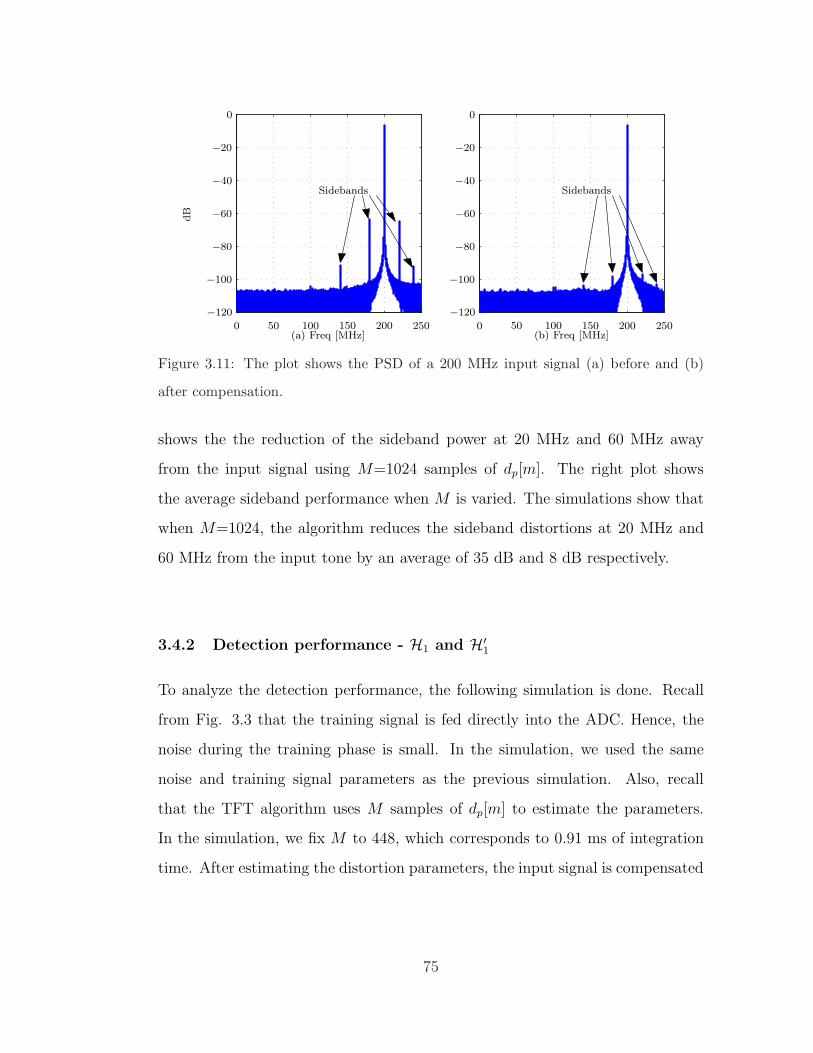
(b) Freq [MHz]
SidebandsdB
(a) Freq [MHz]
Sidebands
0 50 100 150 200 2500 50 100 150 200 250
−120
−100
−80
−60
−40
−20
0
−120
−100
−80
−60
−40
−20
0
Figure 3.11: The plot shows the PSD of a 200 MHz input signal (a) before and (b)
after compensation.
shows the the reduction of the sideband power at 20 MHz and 60 MHz away
from the input signal using M=1024 samples of dp[m]. The right plot shows
the average sideband performance when M is varied. The simulations show that
when M=1024, the algorithm reduces the sideband distortions at 20 MHz and
60 MHz from the input tone by an average of 35 dB and 8 dB respectively.
3.4.2 Detection performance - H1 and H′1
To analyze the detection performance, the following simulation is done. Recall
from Fig. 3.3 that the training signal is fed directly into the ADC. Hence, the
noise during the training phase is small. In the simulation, we used the same
noise and training signal parameters as the previous simulation. Also, recall
that the TFT algorithm uses M samples of dp[m] to estimate the parameters.
In the simulation, we fix M to 448, which corresponds to 0.91 ms of integration
time. After estimating the distortion parameters, the input signal is compensated
75

from input, M = 1024
sideband at 60MHz
Suppression of
from input, M = 1024
sideband at 20MHz
Suppression of
dB
Input freq [MHz]
from input
of sideband at 60MHz
Average suppression
from input
of sideband at 20MHz
Average suppression
M , Length of data dp(m)
dB
50 100 150 200 0 500 10000
5
10
15
20
25
30
35
40
−5
0
5
10
15
20
25
30
35
40
Figure 3.12: The plots show the sideband suppression performance at 20 MHz and 60
MHz away from the input frequency signal and when M is varied.
before spectrum sensing.
During spectrum sensing, we assumed there are strong and weak tones in
the presence of additional noise (e.g., receiver noise). We assume the signals
lie in some frequency bins of the STFT. We set the signal-to-noise ratio (SNR)
of the strong signal and weak signals (in the frequency bin) to 40 dB and -20
dB, respectively. We also set the strong and weak signals at fref = 20 MHz
apart in the frequency domain. Let us denote the frequency of the strong and
weak signal by fa and fb, respectively. Then, we can relate the frequencies as
fb = fa + fref. For example, suppose fa is 100 MHz, then fb is 120 MHZ. Due to
the distortions in the ADC, spurious sidebands from the strong signal are created
in the sampled data. Although the strong and weak signals do not overlap in the
frequency domain, the most dominant spurious sideband does overlap with the
weak signal. From (3.18), we know that the amplitude of the spurious sidebands
76

increases proportionally to frequency. Using the same distortion parameters (C0
and fs) as in the previous simulation, and supposing fa is 100 MHZ, 150 MHz or
200 MHz, the SNR of the dominant spurious sideband is -24 dB, -20 dB or -18
dB, respectively. An energy detector (3.33) is used to detect the weak signal and
the performance before and after using the proposed solution is analyzed. In the
simulation, we fix the length L in the energy detector to 22400. This corresponds
to 45.9 ms of sensing time. The simulation results are averaged over 300 runs.
Figure 3.13 shows the detection performance in terms of PD and PFA when
fa = 100, 150, 200 MHz. The legend is the same for all the plots. We can make
2 observations from the receiver operating characteristics (ROC) curve. First,
the plots show that the theoretical and experimental performance before com-
pensation (H′1) match well. Also, the ROC curve before compensation changes
for different fa. This is due to the fact that the SNR of the dominant spurious
sideband increases with fa and, hence, affects the performance. Note that in the
ideal case (H1), the curve is independent of fa. Second, the proposed solution
improves the detection performance and approaches the ideal case.
We note that there is a crossover point at the lower PFA, which is dependent
on the sensing time. When we increase the sensing time, the ROC curve of the
undistorted case (H1) will shift upwards and the crossover point will move further
to the left. For example, see Fig. 3.19 of Section 3.C where we double the sensing
time and plot the ROC curve.
3.4.3 Detection performance - H2 and H′2
The simulation setup is similar to the previous section using sinusoidal tones.
The main difference is that the tones are replaced by QPSK signals. In this case,
the frequencies fa and fb represent the carrier frequency of the signals. Similarly,
77

H1 - theory
proposed solution
H′
1 - theory
H′
1 - simulated
(c) fa = 200 MHz
PD
PFA
(b) fa = 150 MHz
PD
(a) fa = 100 MHz
PD
0 0.2 0.4 0.6 0.8 1
0 0.2 0.4 0.6 0.8 1
0 0.2 0.4 0.6 0.8 1
0
0.5
1
0
0.5
1
0
0.5
1
PFA
PFA
Figure 3.13: The plots show the PD vs PFA of the weak signal when fa is (a) 100
MHz, (b) 150 MHz or (c) 200 MHz. The plots show the theoretical and simulated
performance before (H′1) and after using the proposed solution. The ideal solution is
H1. The legend is the same for all plots.
we first compare detection performance in terms of PD and PFA. Figure 3.14
shows the ROC curve before and after compensation. In the simulation settings,
the noise power dominates over both the desired signal and the interfering signal.
As such, the ROC curve is almost the same for all cases. The benefits of the
proposed solution is revealed when we examine the threshold γ used in the PD
and PFA for the different cases.
78

H2 - theory
proposed solution
H′
2 - theory
H′
2 - simulated
(c) fa = 200 MHz
PD
PFA
(b) fa = 150 MHz
PD
(a) fa = 100 MHz
PD
0 0.2 0.4 0.6 0.8 1
0 0.2 0.4 0.6 0.8 1
0 0.2 0.4 0.6 0.8 1
0
0.5
1
0
0.5
1
0
0.5
1
PFA
PFA
Figure 3.14: The plots show the PD vs PFA of the weak signal when the carrier fre-
quency fa is (a) 100 MHz, (b) 150 MHz or (c) 200 MHz. The legend is the same for
all plots.
3.4.4 Impact of threshold during sensing
We can derive the threshold γ that corresponds to different PD and PFA through
analysis (using the PFA and PD expressions) or through simulations. Here, we
generate the plots using the simulated results from the previous sections. The
threshold is normalized to the noise power.
Recall that the frequency of the strong signal is selected to be 100 MHz, 150
MHz or 200 MHz. Before using the proposed solution, for a desired constant PD
or PFA, the threshold must vary with the frequency. This can be seen in Fig.
3.15 and Fig. 3.16, which represent the case for sinusoidal tone H1 and QPSK
79

signal H2, respectively.
fa = 200 MHz
fa = 150 MHz
fa = 100 MHz
Proposed solution
Normalised Threshold [dB]
PFA
PD
−0.05 0 0.05 0.1 0.15 0.2
−0.05 0 0.05 0.1 0.15 0.2
0
0.2
0.4
0.6
0.8
1
0
0.2
0.4
0.6
0.8
1
Normalised Threshold [dB]
Figure 3.15: The plots show the normalized threshold used to obtain the various pairs
of PD amd PFA for sinusoidal signals H1.
The curves denoted by fa show the required threshold when the strong signal’s
frequency is fa. The black line with inverted triangle markers shows the threshold
required after using the proposed solution. Note that after compensation, the
required threshold for a fixed detection performance is constant and independent
of fa. Hence, the proposed solution reduces the complexity of finding an adaptive
threshold. Moreover, even when an adaptive threshold is used to obtain a fixed
PFA, the resultant PD may degrade significantly (for example, in H1).
80

Normalised Threshold [dB]
PFA
fa = 200 MHz
fa = 150 MHz
fa = 100 MHz
Proposed solutionPD
−0.1 −0.05 0 0.05 0.1 0.15
−0.1 −0.05 0 0.05 0.1 0.15
0
0.2
0.4
0.6
0.8
1
0
0.2
0.4
0.6
0.8
1
Normalised Threshold [dB]
Figure 3.16: The plots show the normalized threshold used to obtain the various pairs
of PD amd PFA for QPSK signals H2.
3.5 Conclusion
In this chapter, we showed how spurious tones are created in the distorted ADC
samples. We also described a way to use the STFT block to estimate the dis-
tortions and then compensate the samples. Simulations show that the sideband
tones can be estimated and suppressed using the proposed algorithm. The sim-
ulation results show that by increasing the data length, the suppression can be
as much as 35dB. The chapter also investigated the effects of spurious sidebands
on the detection performance in spectrum sensing. Simulations were performed
to analyze the detection performance and theoretical results are derived for ver-
ifications. The results show that compensating for the presence of the spurious
sidebands improves the detection performance in spectrum sensing in a tangible
81
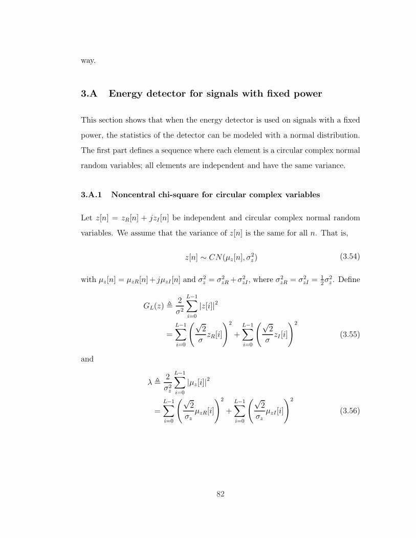
way.
3.A Energy detector for signals with fixed power
This section shows that when the energy detector is used on signals with a fixed
power, the statistics of the detector can be modeled with a normal distribution.
The first part defines a sequence where each element is a circular complex normal
random variables; all elements are independent and have the same variance.
3.A.1 Noncentral chi-square for circular complex variables
Let z[n] = zR[n] + jzI [n] be independent and circular complex normal random
variables. We assume that the variance of z[n] is the same for all n. That is,
z[n] ∼ CN(µz[n], σ2z) (3.54)
with µz[n] = µzR[n]+ jµzI [n] and σ2z = σ2
zR+σ2zI , where σ
2zR = σ2
zI =12σ2z . Define
GL(z) ,2
σ2
L−1∑
i=0
|z[i]|2
=
L−1∑
i=0
(√2
σzR[i]
)2
+
L−1∑
i=0
(√2
σzI [i]
)2
(3.55)
and
λ ,2
σ2z
L−1∑
i=0
|µz[i]|2
=
L−1∑
i=0
(√2
σzµzR[i]
)2
+
L−1∑
i=0
(√2
σzµzI [i]
)2
(3.56)
82

where√2
σzzR[i] ∼ N
(√2
σzµzR[i], 1
)
and√2
σzzI [i] ∼ N
(√2
σzµzI [i], 1
)
. From [60], the
mean and variance of GL(z) are
E[GL(z)] = 2L+ λ (3.57a)
var[GL(z)] = 4(L+ λ) (3.57b)
When L is large, GL(z) can be approximated as a normal distribution.
3.A.2 Energy detector for signals with a fixed power
We define a class of deterministic signals where each member has the same power,
i.e.
Pzs =1
L
L−1∑
i=0
|zs[i]|2 (3.58)
Suppose an energy detector is used to detect this class of signals in the presence
of circular complex white Gaussian noise:
z[n] = zs[n] + zv[n] (3.59)
where zs[n] is a signal in the above class and zv[n] ∼ CN(0, σ2zv) is noise. Then,
we see that
z[n] ∼ CN(zs[n], σ2zv) (3.60)
Also, note that z[n] has the same form as (3.54) when zs[n] = µz[n] and σzv = σz.
Using an energy detector on z[n] and (3.55) yields
TL(z) =1
L
L−1∑
i=0
|z[i]|2
=σ2zv
2LGL(z) (3.61)
83

When L is large, TL(z) has a normal distribution. Using (3.56) to (3.58), the
mean and variance are:
E[TL(z)] = σ2zv + Pzs (3.62a)
var[TL(z)] =σ2zv
L(σ2
zv + 2Pzs)
=1
L[(σ2
zv + Pzs)2 − P 2
zs] (3.62b)
3.B Comparison of various compensation schemes
In this work, the proposed signal compensation algorithm, FOT, is based on a
first-order Taylor series approximation (3.32). Other useful compensation tech-
niques have been proposed [57–59]. This section compares the performance of
the proposed algorithm with these other algorithms. The evaluation is done by
comparing the suppression performance of the spurious sidebands as described in
Section 3.4.1.
Reference [57] proposed the DMC structure based on a Taylor series expres-
sion. Using Taylor series, it shows that the distorted signal can be represented
as the true signal and higher order error terms. The proposed DMC has 3 stages
and removes up to the third-order errors. It is noted that when the derivative
filter is applied on the distorted signal, additional error components are created
and the DMC solution removes them as well. The first stage of the DMC has
the same form as our proposed FOT solution in Fig. 3.9. The second and third
stages, however, use more derivative filters, multipliers and adders. It should
be noted that all the derivative filters have the same filter coefficients. In this
simulation, we implement the DMC using the same filter coefficients we used in
our proposed solution.
84
Reference [58] modifies the conventional Lagrange interpolator to handle ban-
dlimited signals. The interpolator is called the functionally weighted (FW) in-
terpolator and it is of the form
sB(t) ≈1
γ(t)
N∑
k=1
sB(t′k)γ(t
′k)
L(t)
L′(t′k)(t− t′k)(3.63)
where sB(t′k) and t
′k are given. The FW interpolator assumes that the signal sB(t)
is bandlimited and its frequency spectrum lies in [−B/2, B/2]. The algorithm
also assumes that t′k = (p + δp)Ts and |δp| < 1/2, where p = −P + k − 1 and
N = 2P +1. Therefore, the true signal value at t = 0 is estimated as sB(0). The
rest of the functions in (3.63) are defined as
γ(t) =wap(t)Lo(t)
sin(πt/T )(3.64a)
L(t) =
N∏
k=1
t− t′k (3.64b)
L′(t′k) =dL(t)
dt
∣∣∣∣t=t′
k
(3.64c)
where
wap(t) =sinc
(
Bw
√t2 − T 2
w
)
sinc(jBwTw)(3.65a)
Lo(t) =P∏
p=−P
t− pTs (3.65b)
and
Bw =1
Ts− B (3.66a)
Tw = Ts(P + 1) (3.66b)
Hence, given a set of N distorted sampled data w[n], · · · , w[n+N−1] and time
instants tn, · · · , tn+N−1, we can estimate w((n− P )Ts) (denoted as w[n − P ])
85

by defining
t′k = tn+k−1 − (n + P )Ts (3.67a)
sB(t′k) = w[n + k − 1] (3.67b)
and, therefore,
w[n− P ] = sB(0) (3.68)
In the simulation, we set B = 0.8/Ts and P = 12. It is noted that the functions
in the FW interpolator includes evaluations of γ(t) and L′(tk). In [58], there are
details on how to reduce the complexity of evaluating these functions.
In our first simulation, we use the same settings as described in Section 3.4.1,
with two differences. Firstly, we assume that the distorted sampling offsets are
known. Secondly, we fix the frequency of the input sinusoidal signal to 200 MHz.
We assume that the distorted sampling offsets are known because we are only
interested in comparing the various signal compensation algorithm. Also, we fix
the frequency of the input signal to 200 MHz because we know that the magnitude
of the spurious sidebands increases with the input frequency, and hence it is
easier to compare the suppression performance of the various techniques. In this
experiment, we use the proposed FOT algorithm, the DMC algorithm and FW
algorithm.
Figure 3.17 shows a realization of the distorted signal’s spectrum before and
after using the 3 compensation algorithms. From the figure, we see that the
distorted signal contains some spurious sidebands around its input frequency
(200 MHz). The figure also shows that the 3 algorithms are able to remove the
spurious sidebands. The average suppression of the sidebands at 20 MHz away
from the input frequency for FOT, DMC and FW are 40 dB, 40 dB and 42 dB,
respectively. This shows that under the current simulation settings, our proposed
86

Sidebands
FWDMC
FOTDistorted signal
dB
Freq [MHz]
dB
Freq [MHz]dB
Freq [MHz]
dB
Freq [MHz]
150 200 250150 200 250
150 200 250150 200 250
−150
−100
−50
0
−150
−100
−50
0
−150
−100
−50
0
−150
−100
−50
0
Figure 3.17: The plots show the spectrum of the distorted signal and the compensated
signal using the various methods. The distorted signal is generated based on the same
settings in Section 3.4.1. FOT, DMC and FW denote the resulting spectrum after using
the proposed compensation method, [57] and [58], respectively. In these simulations,
the distortion sampling offsets are at most 0.1% of Ts.
compensation algorithm works as well as the techniques in [57,58]; albeit at much
lower computational complexity.
The reason why the advanced techniques do not have a more significant im-
pact on performance than the simpler proposed architecture, is because of the
magnitude of the jitter/sampling offsets. Under the current simulation settings,
the distorted sampling offsets are at most 0.1% of the sampling period (0.1% of
Ts). In the next simulations, we increase the distorted sampling offsets to 1% of
Ts and repeat the experiment. A realization of the new simulation is shown in
Fig. 3.18. The top-left plot shows the frequency spectrum of the distorted signal
87

FW
dB
Freq [MHz]
DMC
Sidebands
dB
Freq [MHz]
FOT
Sidebands
dB
Freq [MHz]
Distorted signal
Sidebands
dB
Freq [MHz]
150 200 250150 200 250
150 200 250150 200 250
−150
−100
−50
0
−150
−100
−50
0
−150
−100
−50
0
−150
−100
−50
0
Figure 3.18: The plots are created using the same settings as the settings in Fig. 3.17,
except that the sampling offsets is 1 order of magnitude larger (i.e. up to 1% of Ts).
before compensation. It can be seen that increasing the sampling offsets creates
additional spurious sidebands. These additional spurious sidebands come from
the higher order error terms in the distorted signal. In this case, we find that
the techniques in [57, 58] can be helpful. The top-right plot of Fig. 3.18 shows
the spectrum of the signal after using our proposed FOT solution. At shown, the
spurious sidebands are not removed completely. The bottom plots in Fig. 3.18
show that the techniques in [57, 58] remove more spurious sidebands. Therefore,
the simulations show that if the sampling offsets increase, then one can use more
advanced techniques to remove the spurious sidebands.
88

3.C Increasing sensing time
The below ROC curve is obtained by doubling the sensing time (L) used in Fig.
3.13. It illustrates that increasing L shift the crossover point further to the left.
(c) fa = 200 MHz
PD
PFA
(b) fa = 150 MHz
PD
PFA
H1 - theoryproposed solutionH′
1 - theoryH′
1 - simulated
(a) fa = 100 MHz
PD
PFA
0 0.2 0.4 0.6 0.8 1
0 0.2 0.4 0.6 0.8 1
0 0.2 0.4 0.6 0.8 1
0
0.5
1
0
0.5
1
0
0.5
1
Figure 3.19: The plots show the PD vs PFA of the weak signal when fa is (a) 100
MHz, (b) 150 MHz or (c) 200 MHz. The plots show the theoretical and simulated
performance before (H′1) and after using the proposed solution.
89

CHAPTER 4
Clock Jitter Compensation in High-Rate ADC
Circuits
Certain applications of modern radios, such as cognitive radios and UWB radios,
require a high signal-to-noise ratio (SNR) in order to detect the presence of
the desired signal from noisy measurements. Unfortunately, signals with high-
frequency content, either due to high bandwidth or high carrier frequencies, are
very sensitive to jitter at the ADC. Clock jitters arise from noise in the clock
generating crystal and phase-locked-loop (PLL). The jitters cause the ADC to
sample the input signal at non-uniform sampling times and introduce distortion
that limits the signal fidelity and degrades the SNR [62]. While the effects of
jitter noise can be neglected at low frequencies, applications requiring enhanced
performance at higher frequencies [32,33,41,63,64] demand higher SNR from the
sampling circuit.
There has already been considerable work in the literature on modeling clock
jitter and understanding its effects [9, 62, 65, 66]. Most models assume the jitter
is Gaussian-distributed with zero mean and with a standard-deviation that is
represented as a percentage of the sampling interval [67]. The models also assume
that clock-jitter (as opposed to aperture jitter) is correlated. This is because the
PLL incorporates a low-pass filter that correlates the jitter. Expressions for
the power-spectral-density (PSD) of the phase-noise output by the PLL appear
90

in [9, 62].
Various approaches have been proposed to treat sampling-clock jitters. Some
approaches interleave several ADCs in order to produce an effective higher sam-
pling rate. This technique, however, introduces other challenges such as mis-
matches in the delays of the clocks fed into the ADCs, mismatches in the gain
of each ADC, and the DC offset between the ADCs (we discuss some of these
problems later in Chapter 5). The works [14–16,68–70] propose techniques to ad-
dress such mismatches in order to allow time-interleaved ADCs to serve reliably
as high-speed ADCs. In [57, 71], alternative approaches for signal compensation
are presented; these approaches, however, assume full knowledge of the jitter it-
self. We do not make this assumption in this work and assume the system must
estimate and compensate for the jitter and its effects. Other approaches [72]
transform the signal into the wavelet domain and use linear least-mean-squares
estimation (LLMSE) techniques to recover the original signal. This approach
assumes that the signal has small support in the wavelet domain, which sim-
plifies the estimation of the covariance matrix used in the LLMSE step to a
diagonal representation. This approach, however, is computationally intensive to
implement—especially at high sampling rates.
Some recent work has focused on the recovery of the jitter through the in-
jection of training tones and on the subsequent compensation of the distorted
data [32, 41, 64, 73]. The schemes proposed in [32, 73] assumed that the input
signal is narrow-band, which is an impractical assumption for ultra-wide-band
and cognitive radio applications. Here, in section 4.1, we first examine the effect
of the clock time jitter on the SNR of the sampled signal [19]. Subsequently, in
sections 4.2 and 4.3, we propose compensation methods based on a signal injec-
tion architecture for direct downconversion architectures. Next, in sections 4.4
91

and 4.5, we analyze the performance of estimation architectures such as those
studied in [32, 41, 64, 73] and of the proposed schemes in some detail. Finally,
section 4.6 shows our simulations results.
In this chapter, we will be using capital letters to denote matrices, small let-
ters to denote vectors and scalars. We will also use boldface notation to denote
random quantities and normal font to denote deterministic (non-random) quan-
tities. We will use the notation x(t) and x[n] , x(nTs) to denote, respectively,
a continuous-time signal and a discrete-time signal sampled with period Ts. A
complex signal x(t) with in-phase and quadrature-phase components xI(t) and
xQ(t), respectively, is modeled with the equivalent notation x(t) , xI(t)+ jxQ(t)
where j ,√−1 is the imaginary unit.
4.1 Problem formulation
The key challenge in this work is to compensate for clock jitters in ADCs with
already small jitters. As explained in the introduction, jitter errors arise when
the input signal is not sampled exactly at multiples of the sampling period, Ts,
but rather at perturbed versions, say, at time instants nTs+e(nTs), where e(nTs)
denotes the amount of random jitter occurring at nTs. An ADC with a clock jitter
of 1% means that the standard-deviation of the jitter e[n] is equal to 0.01Ts (1%
of Ts). Although apparently small, this amount of jitter is problematic when the
sampled signal contains high frequency components due to either having wide
bandwidth or a high carrier frequency; in this work, we concentrate on the case
where the ADC operates at 1GHz in order to sample a wide-bandwidth signal
that resides at baseband. Our objective is to propose filtering and estimation
techniques that would compensate for the effect of the jitter in the sampling
clock and reduce it to the equivalent of operation at about 0.5% jitter for a 10-
92
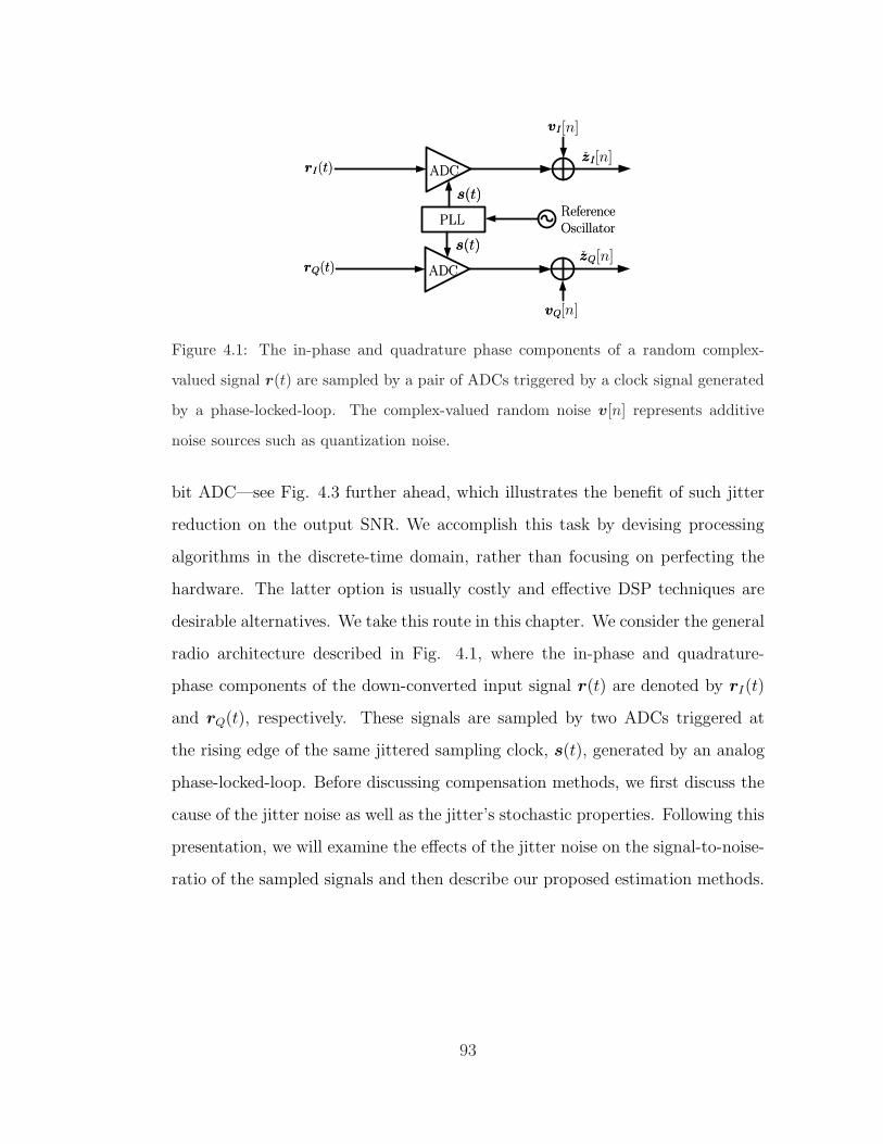
Figure 4.1: The in-phase and quadrature phase components of a random complex-
valued signal r(t) are sampled by a pair of ADCs triggered by a clock signal generated
by a phase-locked-loop. The complex-valued random noise v[n] represents additive
noise sources such as quantization noise.
bit ADC—see Fig. 4.3 further ahead, which illustrates the benefit of such jitter
reduction on the output SNR. We accomplish this task by devising processing
algorithms in the discrete-time domain, rather than focusing on perfecting the
hardware. The latter option is usually costly and effective DSP techniques are
desirable alternatives. We take this route in this chapter. We consider the general
radio architecture described in Fig. 4.1, where the in-phase and quadrature-
phase components of the down-converted input signal r(t) are denoted by rI(t)
and rQ(t), respectively. These signals are sampled by two ADCs triggered at
the rising edge of the same jittered sampling clock, s(t), generated by an analog
phase-locked-loop. Before discussing compensation methods, we first discuss the
cause of the jitter noise as well as the jitter’s stochastic properties. Following this
presentation, we will examine the effects of the jitter noise on the signal-to-noise-
ratio of the sampled signals and then describe our proposed estimation methods.
93

4.1.1 Stochastic properties of the clock jitter
We start by describing the statistical properties of the clock jitter. To do so, we
comment on the connection between the PLL phase-noise and the clock jitter.
Once this connection is defined, and since the statistical properties of PLL phase
noise are well understood and documented in the literature, we can then arrive at
useful expressions for the power spectral density (PSD) of the clock jitter. This
PSD will be helpful in designing estimation and compensation methods for the
jitter.
We model the sampling-clock signal that is generated by the PLL as a sinu-
soidal signal with frequency fs, say,
s(t) = sin(2πfst + φs(t) + θs) (4.1)
In (4.1), the term φs(t) denotes the phase-noise that corrupts the sampling clock,
and θs is some deterministic phase-offset. We model φs(t) as a zero-mean random
process, If the phase-noise is not zero-mean, it is possible to rewrite (4.1) such that
the new phase-noise is zero-mean for a different θs value. Modeling the phase-
noise in this manner is consistent with phase-noise models used in conjunction
with second-order PLL models [74]. We are able to simplify the expression for s(t)
by changing the time reference. To this end, consider setting the time variable in
(4.1) to t = t′ − θs2πfs
. In this case, the equations are similar except that θs = 0.
For this reason, and without loss of generality, we set θs = 0.
We now let the discrete-time random process e[n] denote the jitter that per-
turbs the sampling instants. We denote the actual sampling time instants by tn
and, therefore, write
tn = nTs + e[n] (4.2)
94

When the phase-noise process φs(t) is small and varies slowly relative to the
sampling frequency, it can be verified that the jitter random process e[n] is related
to the phase-noise process φs(t) as follows (see App. 4.A):
e[n] ≈ −φs(nTs)
2πfs(4.3)
Assume the phase-noise has an effective bandwidth of 2πfe radians/second. Then,
it can be shown that the power spectral density (PSD) of the jitter can be ap-
proximated by (see App. 4.A and [75])
Se(ejω) ≈ 1
(2πfs)2Ts
∞∑
k=−∞Sφ
(ω − 2πk
2πTs
)
(4.4)
where
Sφ(f) =βφf
2
(f 2 + f 2e )
2(4.5)
over 0 ≤ ω ≤ 2π and for some constants βe and σ2e = πβe/2fe; the variable σ2
e
denotes the variance of the clock jitter and j is the imaginary unit j ,√−1. The
PSD given by (4.4) is low-pass and decays as ω approaches π. The corresponding
autocorrelation function of the jitter process is given by the sampled inverse
discrete-time Fourier transform of (4.4) (See App. 4.A)
Re(m) ≈ σ2e(1− 2πfe |m|Ts)e−2πfe|m|Ts (4.6)
Moving forward, we express the root-mean-square (RMS) jitter value, σe, as a
percentage of the sampling interval Ts by writing σ2e = (αTs)
2. For example, if
α = 1100
, then the RMS value of the jitter would be 1% of Ts. The jitter will
be modeled as a Gaussian random process with zero-mean and autocorrelation
function Re(m). Figure 4.2(a) plots the PSD of the jitter as given by (4.4).
At this point, we explore up to what frequency the jitter must be recovered in
order to reduce the jitter standard-deviation to a certain level. This computation
95

0 0.1 0.2 0.3 0.4 0.5 0.7 0.810
−4
10−3
10−2
10−1
100
ω (rad)
Norm
alize
dS
e(ω
)
Normalized PSD of jitter vs. Frequency
ωcut
(a) The shape of the PSD of the jitter for
fe = 5MHz and fs = 1GHz. The PSD is
normalized such that its peak value is equal
to one.
0 10 20 30 40 50 60 70 80 90 1000
0.1
0.2
0.3
0.4
0.5
0.6
0.7
0.8
0.9
1
Remaining Jitter as Percent of Ts vs. fcut/fe
fcut/fe
√
E[e
(t)2
]/σ
e
5
(b) An illustration of the expected amount of
jitter reduction as a function of the perfect
recovery frequency ωcut/(2πTs) when fe =
5MHz and fs = 1GHz.
Figure 4.2: The PSD of the jitter using fe = 5MHz, fs = 1GHz as well as the expected
amount of jitter reduction as a function of ωcut.
allows us to evaluate which jitter recovery goals are feasible with digital recovery.
Assume our recovery methods are able to recover well the frequency content of the
jitter up to some frequency ωcut – see Figure 4.2(a). Denote the estimated jitter
by e[n] and the remaining jitter by e[n] = e[n]− e[n]. This means that the data
samples will still contain contributions from the jitter components at frequencies
above ωcut. The power of the remaining jitter can be found by integrating the
PSD of the original jitter from ωcut up to 2π−ωcut and normalizing the result by
2π. We find the RMS value by taking the square root of the result and divide by
the original RMS value in order to get the jitter recovery ratio:√
E [e(t)2]
σe=
1
σe
√
1
2π
∫ 2π−ωcut
ωcut
Se(ejω)dω (4.7)
The difficulty for digital recovery methods can be seen from a plot of (4.7).
Assume the numerical values fs = 1GHz and fe = 5MHz. As seen in Figure
4.2(b), in order to reduce the jitter by a factor of 2 (i.e., for the ratio in (4.7)
96

to evaluate to 0.5), the jitter must be perfectly estimated up to a frequency of
25MHz; the reduction of jitter by a factor of 10 (ratio of 0.1) requires the jitter
to be perfectly estimated up to a frequency of ≈ 350MHz. Although halving the
jitter standard-deviation may be possible in the digital domain, reducing it by
a factor of 10 is generally not feasible due to the presence of interfering signals.
We will see in the next section (specifically Fig. 4.3) how halving the jitter
standard-deviation will improve the SNR of the incoming signal significantly.
Throughout the remainder of the article, we use the following assumptions:
Assumption 4.1. The jitter e[n] is zero-mean Gaussian with standard-deviation
σe = αTs.
Assumption 4.2. The jitter e[n] is small in comparison to the sampling interval
Ts (i.e, α≪ 1).
Assumption 4.3. The jitter e[n] is slowly varying (i.e, fe ≪ fs).
Assumption 4.4. The jitter e[n] is independent of the incoming signal and any
noise in the system.
As noted in App. 4.A, Assumption 4.1 is reasonable when the PLL is locked
with small error [76]. When the PLL is not locked, or when the PLL model is
not well-approximated as a linear system, then Assumption 4.1 will not hold.
Assumption 4.2 also reflects the fact that the jitter is relatively small in practice
in comparison to the sampling period; in fact, it is usually less than 1% of the
sampling period using current technologies for high-speed sampling systems [77].
Assumption 4.3 assumes that the jitter is slowly varying. This assumption can
be controlled by the design of the loop filter of the PLL, which dictates the
bandwidth of the phase-noise at the output of the PLL—see App. 4.B. Finally,
Assumption 4.4 states that the jitter noise is independent of the incoming signal
97

and noise sources in the system, including quantization noise. The jitter may
be weakly dependent with the thermal noise present in the system (since the
phase-noise of the free-running oscillator in the PLL is also affected by thermal
noise). However, it is usually assumed that such dependence is sufficiently weak
and that thermal noise at the input of the ADC is small in comparison to the
incoming signal and other noise in the system.
4.1.2 Effects of the clock jitter
In this section, we investigate the effect of the clock jitter on the sampled data.
We quantify by how much the random shifts in the sampling instants reduce the
signal-to-noise ratio (SNR) at the output of the ADC. We consider two mod-
els for the incoming signal: (1) a complex-sinusoidal tone and (2) a complex
band-limited random signal. We will use the latter case for analysis of signal
degradation in UWB and cognitive radio scenarios. The case of a sinusoidal tone
allows us to analyze the effect of the jitter on training tones that we inject into
the ADC. When other noise sources are ignored, this analysis was previously con-
ducted in, for example, [78] and [79, p.68]. The analysis of the SNR due to only
jitter for band-limited random signals was conducted in [78]. Here we include
other noise sources such as front-end noise and quantization noise, as well as
jitter. The purpose of the discussion below is to highlight the benefit of reducing
the jitter standard deviation in terms of the SNR of the incoming desired signal.
It may not be clear, otherwise, how reducing the jitter by a factor of two would
improve performance.
98

4.1.2.1 Complex Exponential Input Signal
We consider first the case of a deterministic complex-sinusoidal incoming signal
r(t) with amplitude Ar and frequency fr:
r(t) = Arej(2πfrt+θr) (4.8)
The samples of r(t) corrupted by the jitter and additive noise source v[n] can be
written as (see Fig. 4.1 and (4.66) in App. 4.A):
z[n] ≈ r
(
t− φs(t)
2πfs
)∣∣∣∣t=nTs
+ v[n] (4.9)
where v[n] denotes complex-valued noise, such as quantization and front-end
noise. Note that we are denoting z[n] with boldface notation as this signal is
random due to the presence of the jitter e[n] and the random noise v[n]. The
signal r[n] with no distortion is denoted by normal font. By using the first order
Taylor series, we have
r
(
t− φs(t)
2πfs
)∣∣∣∣t=nTs
= r
(
nTs −φs(nTs)
2πfs
)
≈ r(nTs)−φs(nTs)
2πfsr(nTs)
≈ r[n] + e[n]r[n] (4.10)
where r(t) denotes the derivative of r(t) evaluated at time t, and e[n] ≈ −φs(nTs)2πfs
by (4.3). Substituting (4.10) into (4.9), we have:
z[n] ≈ r[n] + e[n]r[n] + v[n] (4.11)
where the notation r[n] denotes
r[n] ,d
dtr(t)
∣∣∣∣t=nTs
99

0% 0.2% 0.4% 0.6% 0.8% 1%35
40
45
50
55
60
65
σe (% of Ts)
SNR
(dB)
SNR for sinusoidal signal as a function of σe
(a) SNR vs. σe for complex-sinusoidal signals.
0% 0.2% 0.4% 0.6% 0.8% 1%40
45
50
55
60
σe (% of Ts)
SNR
(dB)
SNR for bandlimited signal as a function of σe
(b) SNR vs. σe for bandlimited signals.
Figure 4.3: In (a), (b), we show the relationship between SNR and σe for complex-
sinusoidal signals and bandlimited signals, respectively. The parameters include: Br =
fr = 200MHz, Ar = 1, σr = 0.548, Ts = 1ns, and σ2v = 2
3·410 . This noise variance
corresponds to the quantization noise power for a 10-bit ADC.
Expression (4.11) reveals how jitter and and other noise sources distort the sample
value. Using the fact that the power of the complex tone r(t) is A2r , the resulting
SNR at the output of the sampler is:
SNR ≈ A2r
(2πfrArσe)2 + σ2
v
(4.12)
Expression (4.12) was derived in [78] and [79, p.68] when σ2v = 0. Figure 4.3(a)
plots the SNR degradation vs. σe. Observe that the SNR degrades quickly with
σe and the jitter becomes the dominant noise source as (2πfrArσe)2 becomes
larger than σ2v . Observe that a reduction of the jitter standard deviation from
1% of the sampling period to 0.5% of the sampling period yields approximately
6dB in SNR improvement for a complex sinusoid with the listed parameters.
100

4.1.2.2 Band-limited Random Signal
We now examine the effect of jitter on a zero-mean wide-sense-stationary (WSS)
random process, r(t), with auto-correlation function Rr(τ) where Rr(0) = σ2r .
Again, similar to (4.11), we get
z[n] ≈ r[n] + e[n]r[n] + v[n] (4.13)
The SNR after sampling is given by
SNR ≈ σ2r
σ2e · E |r[n]|2 + σ2
v
(4.14)
In order to evaluate the power of the derivative we assume that r(t) is mean-
square continuous, i.e.,
E |r(t)|2 <∞, lims→t
E |r(s)− r(t)|2 = 0.
For such a process, it holds that [80]:
Rr(τ) = − d2
dτ 2Rr(τ) (4.15)
in terms of the auto-correlation function of the process r(t). From this result, it
follows that
E |r[n]|2 = Rr(0) = − d2
dτ 2Rr(τ)
∣∣∣∣τ→0
(4.16)
so that (4.14) becomes
SNR ≈ σ2r
−σ2e · d2
dτ2Rr(τ)
∣∣τ→0
+ σ2v
(4.17)
For illustration purposes, consider a bandlimited signal r(t) with box-car power
spectral density (PSD) and sinc autocorrelation function:
Sr(f) =σ2r
2Br
rect
(f
2Br
)
(4.18)
101

where
rect(a) =
1, |a| < 12
12, |a| = 1
2
0, otherwise
(4.19)
and 2Br is the passband bandwidth of the signal r(t) in Hz. Then
Rr(τ) =
σ2rsin(2Brπτ)
2Brπτ, τ 6= 0
σ2r , τ = 0
(4.20)
which is derived by taking the inverse Fourier transform of the PSD Sr(f). It
follows that
− d2
dτ 2Rr(τ)
∣∣∣∣τ→0
=4
3π2B2
rσ2r (4.21)
and the SNR expression (4.17) gives
SNR ≈ σ2r
13(2πBrσrσe)
2 + σ2v
(4.22)
Observe that when the jitter noise dominates the noise v[n], the SNR is deter-
mined solely by the variance of the jitter σ2e and the bandwidth of the incoming
signal Br (σ2r is eliminated). Expression (4.22) was derived in [78] when σ2
v = 0.
The effect of jitter on the SNR is illustrated in Figure 4.3(b). We choose
the per-channel standard-deviation of the signal r(t) by assuming the signal is
Gaussian and the probability of exceeding an absolute-value amplitude of each
channel of one is less than 1% since it is assumed that the ADC has a range of
±1. That is, we select the single-channel standard-deviation σSCr such that:
Q
(1
σSCr
)
≤ 1
200=⇒ σSC
r ≤ 1
Q−1(
1200
) ≈ 0.388 (4.23)
where
p = Q(x) ,∫ ∞
x
1√2πe−
u2
2 du
102

is the standard Q-function and x = Q−1(p) is the inverse Q-function. Assuming
the data on each channel is independent, the total signal standard-deviation σr
becomes σr =√2σSC
r . Figure 4.3(b) again shows that the clock jitter reduces
the SNR considerably if left uncompensated. Also notice that a reduction of the
jitter standard deviation from 1% of the sampling period to 0.5% of the sampling
period yields approximately 5.5dB in SNR improvement for a bandlimited signal
with the listed parameters. In the next section, we derive methods for estimating
the jitter e[n] that will be used for the compensation of the jittered samples.
4.2 Estimation of clock jitter
As illustrated in the previous section, the sampling jitter has an adverse effect
on the SNR of the ADC. In this section, we propose methods to estimate the
jitter sequence, e[n]. We propose a signal injection algorithm for wideband re-
ceivers similar to the technique we proposed earlier in [41,64] and independently
by [32,33,73]. There is however a fundamental difference between our techniques
and other related works such as [32, 33]. While our approach and the approach
taken in [32,33] rely on the use of a reference signal injection outside the received
signal band (we explain why it is useful to inject such training tones in App. 4.C.),
the problem studied in this paper is not the same as the one discussed in [32,33].
In these references, the receiver sub-samples the incoming narrow-bandwidth RF
signal and a reference tone using a low sampling rate. The incoming signal then
folds down to an intermediate frequency and is subsequently digitally processed.
We do not assume that the incoming signal has a narrow bandwidth; in fact, we
assume that the incoming signal has a wide bandwidth. This is a key difference
between the two approaches and this fact presents new challenges and difficulties
in the signal injection step. First, it is not possible to inject a low-frequency
103

signal anymore along with the down-converted signal since the down-converted
signal now has a wide bandwidth and will interfere with the reference tone (and
vice versa). It is also challenging to generate a clean sinusoid (with negligible
phase-noise) at high-frequencies. For this reason, we must propose a signal in-
jection architecture that is able to produce a relatively clean sinusoid outside the
desired signal bandwidth. Second, the jitter estimation algorithm from [32, 33]
requires the use of tan−1(·) blocks. Such blocks generally consume considerable
power and introduce delay in the system. We avoid this problem by performing
some processing off-line (at the system start-up) and proceed with low-complexity
estimation in real-time. Finally, the compensation method proposed in [32, 33]
effectively only compensates the carriers of the bandpass signals, and not the sig-
nals themselves, since it is assumed that the signals are narrowband and thus the
dominant jitter effects act on the carriers and not the signals. Since we assume
that the incoming signal is wide-band, we must compensate the signal itself for
the jitter effects.
For all these reasons, we replace the radio architecture of Fig. 4.1 with Fig.
4.4 where a training signal y(t) is generated inside the radio and injected along
with the downconverted received signal r(t). The samples at the output of the
ADCs constitute the in-phase and quadrature-phase components of the perturbed
signal z[n]. We focus our discussion on “Direct Downconversion Receivers1”. We
will describe a direct recovery method and an optimal jitter recovery scheme
based on the minimization of a mean-square-error cost.
1ADirect-Downconversion Receiver performs an analog quadrature down-conversion to base-band of the signal of interest. The base-band signal is then sampled at a rate at least twice thebandwidth of the signal per channel. [79, p.43]
104

Figure 4.4: Proposed signal injection architecture used for jitter estimation.
4.2.1 Direct downconversion receiver
When the received radio signal r(t) is a wide-band radio signal at baseband
(downconverted in the circuit), it is not possible to inject the training signal y(t)
in the low-frequency region as it will interfere with r(t). For this reason, we
must inject y(t) at high-frequency. Unfortunately, it is generally not practical to
generate a noise-free training signal y(t) at high-frequency. It is, however, feasible
to up-convert a low-frequency training signal with a high-frequency carrier. To
choose the carrier signal, we rely on a frequency-halved sampling-clock. Thus, let
s(t) denote the sampling clock signal that is generated by the PLL–recall (4.1):
s(t) = sin (2πfst+ φs(t)) (4.24)
where fs is the sampling frequency and φs(t) is the phase-noise. Now a scaled,
frequency-halved clock signal, which we shall denote by p(t), will have the form
p(t) = Ap sin
(
2πfs2(t− τp) +
φs (t− τp)
2
)
(4.25)
where τp models some constant delay implemented in the circuit and Ap is a scal-
ing factor. The frequency division is a low-noise, simple integer frequency divider
that preserves the time jitter e[n] and halves the phase-noise φs(t) [40, p.159].
105

When τp is relatively small, we can say that the delayed signal φs (t− τp) is ap-
proximately the same as φs(t) since we have assumed earlier in Assumption 4.3
that the phase-noise is relatively slow compared to the sampling time. Sampling
p(t) with s(t) gives p[n] = p (nTs + e[n]) where e[n] is given by (4.3). Thus, we
can write the samples p[n] as
p[n] = Apsin
(
2πfs2(nTs+e[n]−τp)+
φs (nTs+e[n]−τp)2
)
≈ Ap sin
(
2πfs2(nTs + e[n]− τp) +
φs[n]
2
)
= ej2π(fs2 )nTs (4.26)
where the first equality is due to (4.67), the second approximation is a con-
sequence of (4.3) and the fact that the jitter is small (Assumption 4.2) and
slow (Assumption 4.3) and the last equality is a consequence of choosing Ap =
− csc(2π fs
2τp)where csc(x) , 1/ sin(x). Thus, we observe that the samples of
the signal derived by frequency-halving the sampling-clock and with negligible
delay will have no jitter; it is approximately deterministic. Notice that p[n] is
a real signal that we represented as a complex signal, which will be used for
convenience in (4.28)-(4.30).
We now modulate p(t) by a low-frequency, low-noise training tone w(t) in
order to up-convert w(t) to become a high-frequency training signal without the
difficulty of generating it as a high-frequency signal directly. Thus, we choose the
training signal for the direct-downconversion receiver to be:
y(t) = w(t)p(t) (4.27)
106

and the corresponding samples of the training signal become
y[n] , y(nTs + e[n])
= w (nTs + e[n]) p[n]
≈ w (nTs + e[n]) ej2π( fs
2 )nTs (4.28)
We chose the tone w(t) to be a low-frequency complex-sinusoid:
w(t) , Awej(2πfwt+θw) (4.29)
Then, by substituting (4.29) into (4.28), we can show that the sampled injected
signal y[n] will be a complex-sinusoid located at fs2+ fw:
y[n] ≈ w (nTs + e[n]) ej2π( fs
2 )nTs
= Awej(2π( fs
2+fw)nTs+2πfwe[n]+θw) (4.30)
Figure 4.5 illustrates the tone injection scheme. The training tone y(t) is injected
along with the desired signal r(t) to form the complex-valued signal z(t):
z(t) , r(t) + y(t) (4.31)
The composite signal z(t) is then sampled by the ADC to yield the complex-
valued discrete-time signal z[n]:
z[n] , z(nTs + e[n]) + v[n] (4.32)
where v[n] is noise introduced at the ADC, which includes quantization noise.
4.2.2 Direct jitter estimation
We assume that we are able to estimate θw as θw say, by using a digital PLL
technique [81] up to an ambiguity term that is a multiple of 2π (see App. 4.D). A
107
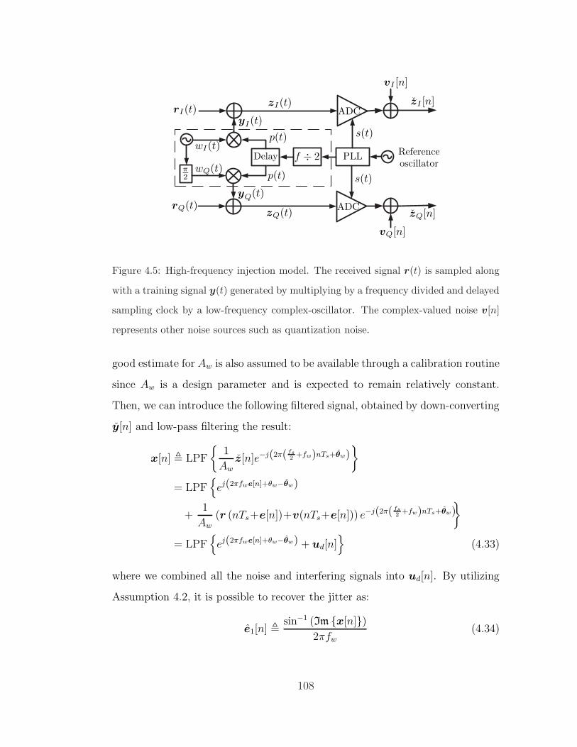
Figure 4.5: High-frequency injection model. The received signal r(t) is sampled along
with a training signal y(t) generated by multiplying by a frequency divided and delayed
sampling clock by a low-frequency complex-oscillator. The complex-valued noise v[n]
represents other noise sources such as quantization noise.
good estimate for Aw is also assumed to be available through a calibration routine
since Aw is a design parameter and is expected to remain relatively constant.
Then, we can introduce the following filtered signal, obtained by down-converting
y[n] and low-pass filtering the result:
x[n] , LPF
1
Aw
z[n]e−j(2π( fs2+fw)nTs+θw)
= LPF
ej(2πfwe[n]+θw−θw)
+1
Aw
(r (nTs+e[n])+v(nTs+e[n])) e−j(2π( fs
2+fw)nTs+θw)
= LPF
ej(2πfwe[n]+θw−θw) + ud[n]
(4.33)
where we combined all the noise and interfering signals into ud[n]. By utilizing
Assumption 4.2, it is possible to recover the jitter as:
e1[n] ,sin−1 (Im x[n])
2πfw(4.34)
108
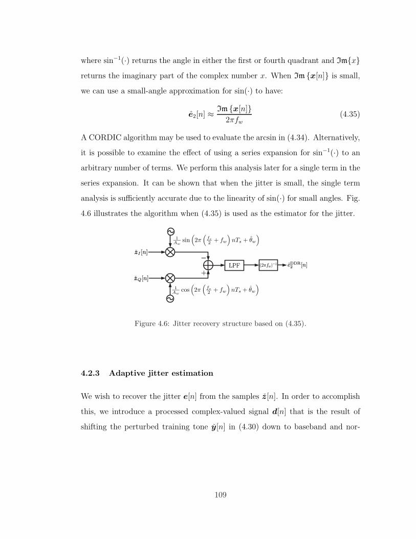
where sin−1(·) returns the angle in either the first or fourth quadrant and Imxreturns the imaginary part of the complex number x. When Im x[n] is small,
we can use a small-angle approximation for sin(·) to have:
e2[n] ≈Im x[n]
2πfw(4.35)
A CORDIC algorithm may be used to evaluate the arcsin in (4.34). Alternatively,
it is possible to examine the effect of using a series expansion for sin−1(·) to an
arbitrary number of terms. We perform this analysis later for a single term in the
series expansion. It can be shown that when the jitter is small, the single term
analysis is sufficiently accurate due to the linearity of sin(·) for small angles. Fig.
4.6 illustrates the algorithm when (4.35) is used as the estimator for the jitter.
Figure 4.6: Jitter recovery structure based on (4.35).
4.2.3 Adaptive jitter estimation
We wish to recover the jitter e[n] from the samples z[n]. In order to accomplish
this, we introduce a processed complex-valued signal d[n] that is the result of
shifting the perturbed training tone y[n] in (4.30) down to baseband and nor-
109

malizing its amplitude by dividing by the factor Aw:
d[n] ,1
Aw
z[n]e−j2π( fs2+fw)nTs
= ej(2πfwe[n]+θw) + ua[n] (4.36)
where the complex-valued noise ua[n] is defined as
ua[n] ,1
Aw
(r[n] + v(nTs + e[n]))e−j2π( fs
2+fw)nTs
We now write down a stochastic optimization problem that allows us to recover
the jitter e[n]. We note that the data signal d[n] in (4.36) is a complex-sinusoid
at baseband and we assume that the jitter e[n] is slowly varying and that most
of its power lies at low-frequencies (as assumed in Assumption 4.3). We let the
phase of the complex sinusoid in (4.36) be denoted by θ:
θ , 2πfwe[n] + θw (4.37)
We estimate θ by solving the following minimum mean-square-error problem: [42,
p.163].
JMSE (θ) = E
[
LPF∣∣d[n]− ejθ
∣∣2]
(4.38)
The low-pass filter removes the out-of-band noise caused by the incoming signal
r[n] , r(nTs+e[n]) and the broadband noise v(nTs+e[n]) while retaining most
of the power of the jitter process. In order to minimize (4.38) iteratively, we
implement a stochastic gradient-descent algorithm that moves along the opposite
direction of the gradient of (4.38) at each iteration. Thus, we compute the
gradient as:
∇JMSE(θ) = E[LPF
jd[n]e−jθ
]+ E
[LPF
−jd∗[n]ejθ
]
= −2E[LPF
Imd[n]e−jθ
](4.39)
110

and the algorithm is given by:
θ[n+ 1] = θ[n] + µE[
LPF
Im
d[n]e−jθ[n]]
(4.40)
where µ is a small positive step-size and θ[n] is the estimate for θ at iteration n. It
is possible to use an instantaneous approximation for the gradient by eliminating
the expectation operation in (4.40) [42, p.165]:
E
[
LPF
Im
d[n]e−jθ[n]]
≈ LPF
Im
1
Aw
z[n]e−j(2π( fs2+fw)nTs+θ[n])
(4.41)
where z[n] denotes the actual realization of the random process z[n]. Also, since
we are only interested in the imaginary part, we compute the expression for it
directly as:
E
[
LPF
Im
d[n]e−jθ[n]]
≈ 1
Aw
LPF
zQ[n] cos
(
2π
(fs2+ fw
)
nTs + θ[n]
)
−
zI [n] sin
(
2π
(fs2+ fw
)
nTs + θ[n]
)
(4.42)
where zI [n] and zQ[n] are the in-phase and quadrature phase components of z[n].
Since the training signal will have some constant phase shift due to θw, we recover
the instantaneous jitter from θ[n] (4.37) as:
e3[n] =θ[n]− θ[n]
2πfw(4.43)
The running average θ[n] can be estimated using a forgetting factor filter such
as:
θ[n+ 1] = λθ[n] + (1− λ)θ[n] (4.44)
where λ is a forgetting factor close to one. The block diagram for the adaptive
jitter recovery method is presented in Fig. 4.7.
111
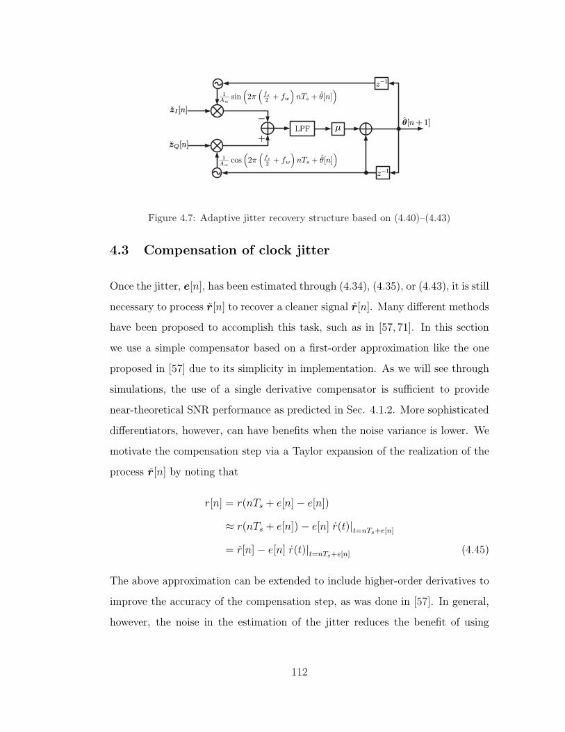
Figure 4.7: Adaptive jitter recovery structure based on (4.40)–(4.43)
4.3 Compensation of clock jitter
Once the jitter, e[n], has been estimated through (4.34), (4.35), or (4.43), it is still
necessary to process r[n] to recover a cleaner signal r[n]. Many different methods
have been proposed to accomplish this task, such as in [57, 71]. In this section
we use a simple compensator based on a first-order approximation like the one
proposed in [57] due to its simplicity in implementation. As we will see through
simulations, the use of a single derivative compensator is sufficient to provide
near-theoretical SNR performance as predicted in Sec. 4.1.2. More sophisticated
differentiators, however, can have benefits when the noise variance is lower. We
motivate the compensation step via a Taylor expansion of the realization of the
process r[n] by noting that
r[n] = r(nTs + e[n]− e[n])
≈ r(nTs + e[n])− e[n] r(t)|t=nTs+e[n]
= r[n]− e[n] r(t)|t=nTs+e[n] (4.45)
The above approximation can be extended to include higher-order derivatives to
improve the accuracy of the compensation step, as was done in [57]. In general,
however, the noise in the estimation of the jitter reduces the benefit of using
112

higher derivatives (the work in [57] assumes that the jitter is perfectly estimated).
The derivative of the realization r(t) is not available after sampling. However,
consider the derivative of r(
t− φs(t)2πfs
)
evaluated at t = nTs:
dr(t− φs(t)2πfs
)
dt
∣∣∣∣∣t=nTs
= r(t)|t=nTs+e[n]
(
1− φs(t)
2πfs
∣∣∣∣∣t=nTs
)
where − φs(t)2πfs
∣∣∣t=nTs
≈ e[n] due to (4.3). If φs(t) is assumed to be small and
slowly varying (in comparison to the sampling frequency), as effectively assumed
in Assumptions 4.1, 4.2 due to (4.3), it is possible to ignore the term φs(t)2πfs
∣∣∣t=nTs
and writedr(t− φs(t)
2πfs)
dt
∣∣∣∣∣t=nTs
≈ r(t)|t=nTs+e[n] (4.46)
It is then possible to create a discrete differentiator [56] in order to approximate
the derivative. A simple example that was used in the simulations is the central
difference differentiator [82]:
dr(
t− φs(t)2πfs
)
dt
∣∣∣∣∣∣t=nTs
≈ − r(n− 5)
1260Ts+
5r(n− 4)
504Ts− 5r(n− 3)
84Ts+
5r(n− 2)
21Ts− 5r(n− 1)
6Ts+
5r(n+ 1)
6Ts−
5r(n+ 2)
21Ts+
5r(n + 3)
84Ts− 5r(n + 4)
504Ts+
r(n+ 5)
1260Ts(4.47)
A more sophisticated differentiator design may yield the same results as a long
impulse response filter with fewer taps [56, 83]. In practice, a low-pass filter is
placed prior to the derivative filter to suppress noise at high-frequencies. We first
recover the signal r[n] as
r[n] ≈ LPF z[n] (4.48)
113

We then apply (4.45) by replacing e[n] by its estimate e[n] found using any of
the methods in the previous section and the derivative approximation (4.46) to
recover the estimate r[n] of the signal r[n]:
r[n] , r[n]− e[n]dr(
t− φs(t)2πfs
)
dt
∣∣∣∣∣∣t=nTs
(4.49)
The architecture for a single derivative reconstruction is illustrated in Fig. 4.8.
Figure 4.8: Proposed compensation algorithm (4.49).
4.4 Mean-square-error analysis
In this section, we analyze the mean-square-error (MSE) performance of the si-
nusoidal tone injection methods described in Sec. 4.2. The analysis will be
performed in the following subsection for the direct jitter estimation method
described in section 4.2.2 and in the next subsection for the adaptive jitter esti-
mation method described in section 4.2.3.
4.4.1 Direct estimation method
Although the analysis in this section is performed for the estimator in (4.35), the
derivation can be extended to a higher number of terms used in the approximation
114

of the sin−1(·) function in order to extend the analysis to the estimator in (4.34).
To begin with, we substitute (4.33) into (4.35) to obtain
e2[n] =1
2πfwLPF
sin(
2πfwe[n] + θw
)
+ ud[n]
(4.50)
We wish to compute the error:
e[n] , e[n]− e2[n]
= e[n]− 1
2πfwLPF
sin(
2πfwe[n] + θw
)
+ ud[n]
(4.51)
We illustrate the above system in Fig. 4.9(a), where F (z) represents the response
of the low-pass filter. We note that this system is not a linear system. For this
reason, we use a common approximation method frequently used in the analysis of
PLLs where we assume that the argument of the sin(·) function is small, and thus
we can linearize the model by using a small angle approximation, as illustrated
in Fig. 4.9(b).
Assuming all input signals are independent of each other, it is possible to
use superposition to evaluate the average power of the output e[n]. We take
advantage of Parseval’s theorem for discrete-time Fourier transforms to write the
mean-square-error as shown in (4.52).
σ2e ≈ 1
2π
∫ π
−π
∣∣1− F (ejω)
∣∣2Se(e
jω)dω
+1
(2πfw)21
2π
∫ π
−π
∣∣F (ejω)
∣∣2 (Su(e
jω) + Sθ(ejω))dω (4.52)
In (4.52), Su(ejω) and Sθ(e
jω) are the PSDs of ud[n] and θw[n], respecively. The
MSE is dominated by terms that are dependent on the design of the phase-
recovery method and on the low-pass filter F (z) used in the final step of the
recovery method, respectively. Thus, if the noise terms dominate the rest, then
it is unnecessary to invest the computational power in computing the sin−1(·)
115

(a) Nonlinear system to model jitter error e[n] as function of input jitter
e[n] and noise ud[n].
(b) Approximate linear system to model jitter error e[n] as function of input
jitter e[n] and noise ud[n].
Figure 4.9: (a) shows the nonlinear system model while (b) shows the linearized time-
invariant system.
operation as suggested by (4.34) and expression (4.35) would be sufficient. Care
must be taken during the design of the PLL as discussed in Sec. 4.1.1 since
the loop-bandwidth of the PLL can determine upper limits on the estimation
capability of any recovery method. Thus, some investment in the PLL can be
beneficial as it allows the bandwidth of the low-pass filter to be reduced and
relaxes the demands on the analog circuit that generates the training tone.
4.4.2 Adaptive estimation methods
In this section, we analyze the performance of the adaptive estimation method
in Fig. 4.7 presented in section 4.2.3. The recovery algorithm closely mirrors the
equations of a digital PLL [84]. Thus, we can analyze the tracking performance
of the loop by considering the equivalent phase-domain model presented in Fig.
116
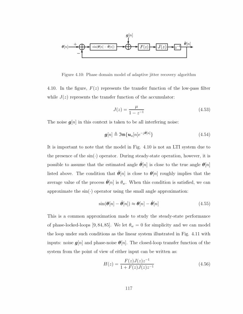
Figure 4.10: Phase domain model of adaptive jitter recovery algorithm
4.10. In the figure, F (z) represents the transfer function of the low-pass filter
while J(z) represents the transfer function of the accumulator:
J(z) =µ
1− z−1(4.53)
The noise g[n] in this context is taken to be all interfering noise:
g[n] , Imua[n]e−jθ[n] (4.54)
It is important to note that the model in Fig. 4.10 is not an LTI system due to
the presence of the sin(·) operator. During steady-state operation, however, it is
possible to assume that the estimated angle θ[n] is close to the true angle θ[n]
listed above. The condition that θ[n] is close to θ[n] roughly implies that the
average value of the process θ[n] is θw. When this condition is satisfied, we can
approximate the sin(·) operator using the small angle approximation:
sin(θ[n]− θ[n]) ≈ θ[n]− θ[n] (4.55)
This is a common approximation made to study the steady-state performance
of phase-locked-loops [9, 84, 85]. We let θw = 0 for simplicity and we can model
the loop under such conditions as the linear system illustrated in Fig. 4.11 with
inputs: noise g[n] and phase-noise θ[n]. The closed-loop transfer function of the
system from the point of view of either input can be written as:
H(z) =F (z)J(z)z−1
1 + F (z)J(z)z−1(4.56)
117
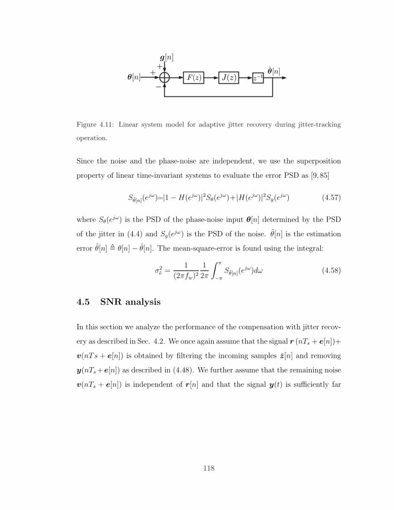
Figure 4.11: Linear system model for adaptive jitter recovery during jitter-tracking
operation.
Since the noise and the phase-noise are independent, we use the superposition
property of linear time-invariant systems to evaluate the error PSD as [9, 85]
Sθ[n](ejω)=|1−H(ejω)|2Sθ(e
jω)+|H(ejω)|2Sg(ejω) (4.57)
where Sθ(ejω) is the PSD of the phase-noise input θ[n] determined by the PSD
of the jitter in (4.4) and Sg(ejω) is the PSD of the noise. θ[n] is the estimation
error θ[n] , θ[n]− θ[n]. The mean-square-error is found using the integral:
σ2e =
1
(2πfw)21
2π
∫ π
−π
Sθ[n](ejω)dω (4.58)
4.5 SNR analysis
In this section we analyze the performance of the compensation with jitter recov-
ery as described in Sec. 4.2. We once again assume that the signal r (nTs + e[n])+
v(nTs + e[n]) is obtained by filtering the incoming samples z[n] and removing
y(nTs+e[n]) as described in (4.48). We further assume that the remaining noise
v(nTs + e[n]) is independent of r[n] and that the signal y(t) is sufficiently far
118

away from r(t). In this case, we describe the recovered samples as
r[n] = r (nTs + e[n]) + v(nTs + e[n])−N∑
i=1
(e[n])i
i!
di
dtir(t+ e[n])
∣∣∣∣t=nTs
= r[n] +∞∑
i=1
(e[n])i
i!
di
dtir(t)
∣∣∣∣t=nTs
+ v(nTs + e[n])
−N∑
i=1
(e[n])i
i!
di
dtir(t+ e[n])
∣∣∣∣t=nTs
(4.59)
We subtract r[n] from the above expression to find:
r[n]− r[n] ≈ v(nTs + e[n]) +N∑
i=1
(e[n])i − (e[n])i
i!
di
dtir(t)
∣∣∣∣t=nTs
+
∞∑
i=N+1
(e[n])i
i!
di
dtir(t)
∣∣∣∣t=nTs
≈ v(nTs+e[n]) + (e[n]− e[n]) d
dtr(t)
∣∣∣∣t=nTs
(4.60)
where the first approximation follows our argument in Sec. 4.3 regarding the
derivative of r(
t− φs(t)2πfs
)
and the second approximation is due to the fact that
the first term in the summation has the highest magnitude in comparison to the
rest. From this, we can compute the MSE in the recovery of r[n] as
E[(r[n]− r[n])2
]≈ σ2
v + σ2e · E
[(d
dtr(t)
∣∣∣∣t=nTs
)2]
(4.61)
where σ2e can be computed using the analysis in Sec. 4.4. Thus, the SNR can be
written as
SNR ≈ σ2r
σ2v + σ2
e · E[(
ddtr(t)
∣∣t=nTs
)2] (4.62)
If we assume that r[n] has the auto-correlation function defined by (4.15), we
can use the result of App. 4.E to find that
E
[∣∣∣∣
dN
dtNr(t)
∣∣∣∣t=nTs
∣∣∣∣
2]
=(π2Br)
2N
2N + 1σ2r , (4.63)
119

which allows us to conclude that the SNR in the compensation can be written as
SNR ≈ σ2r
σ2v +
13(2πBrσrσe)
2 (4.64)
4.6 Simulation results
We assume a sampling period of Ts = 1ns. The jitter e[n] is modeled as described
in Sec. 4.1.1 and is Gaussian with mean zero and standard deviation σe = αTs.
The jitter is correlated and has bandwidth of fe. The default parameters are listed
in Table 4.1. We simulate the recovery methods for sinusoidal signal injection
Table 4.1: Table listing the default values for parameters in the simulation
Parameter α fe σ2v At ft fs λ Br
Default Value 1100
5MHz 13·410 2−4 100MHz 1GHz 255
256200MHz
described under Sec. 4.2.1. Central-derivative filters are used throughout the
simulation (specifically, the 11-tap filter listed in (4.47)). For the simulation of
the band-limited signal, a cut-off bandwidth of Br = 200MHz is chosen and the
signal is generated by filtering white Gaussian noise with the use of a 256-tap
FIR low-pass filter designed using the FIRLS function in MATLAB. The band-
limited signal was jittered by including ten terms of the Taylor series expansion
by adding e[n]i
i!r(i)[n] for the i-th term and the derivative signal r(i)[n] is generated
by applying a central-difference discrete derivative filter to the signal r[n].
In this section, we evaluate the performance of the sinusoidal tone injection
methods discussed in Sec. 4.2. The normalized PSD of the input signal r[n] is
illustrated in Fig. 4.12. Figure 4.13(a) shows the performance of the estimators.
Both algorithms utilize a 4-th order Butterworth IIR low-pass filter designed with
120

Figure 4.12: Normalized PSD of input signal r[n] used in the simulation.
appropriately chosen bandwidths and for the case of the adaptive methods, an
appropriately chosen gain µ to minimize the MSE. The bandwidth of the low-
pass-filter must be reduced as the initial jitter standard-deviation σe is decreased
in general. We fix the low-pass filter in this work to provide smooth theoretical
and simulation curves. The cut-off of this low-pass filter will inherently limit the
performance of the filter to the performance illustrated in Fig. 4.2(b) even as the
low-pass filter becomes ideal. It can be seen from Fig. 4.13(a) that there is a clear
improvement in the MSE by using either of the proposed compensation methods
for moderate values of σe. We also note that the adaptive algorithm in (4.43)
outperforms the direct method in (4.35). We also compare to the estimation
algorithm used in [32,33] that used a tan−1(·) operation to recover the jitter from
(4.33). We notice that the simple estimator in (4.35) performs at the same level
as the estimation algorithm that utilizes the tan−1(·) operation.
We use (4.64) in order to plot the theoretical SNR curves that correspond to
the compensation of a box-car PSD random signal with simulation parameters
listed in Table 4.1 and for a 10-bit ADC. Fig. 4.13(b) illustrates the relative
121

(a) Figure illustrating the MSE in estimating
the jitter e[n] vs. σe tradeoff for the direct
estimation method in (4.35) and the adaptive
method in (4.43). The uncompensated jitter
e[n] is also displayed.
(b) Figure illustrating the SNR after compen-
sation vs. σe tradeoff for the direct estimation
method in (4.35) and the adaptive method in
(4.43). The SNR for the uncompensated sig-
nal is also displayed.
Figure 4.13: In (a), we illustrate the simulated and theoretical MSE in the estimation
of the jitter using the direct and adaptive techniques. In (b), we illustrate the expected
SNR as a result of jitter compensation.
performance of the estimators and the compensation algorithm described in Sec.
4.3 for varying values of σe. It can be seen from the figure that there is a clear
improvement in the SNR by using either of the proposed compensation methods.
We also note that the adaptive algorithm in (4.43) outperforms the direct method
in (4.35). In general, the shape of the PSD of the signal r(t) dictates the slope of
the SNR curve as seen by the difference in the SNR curves for complex-sinusoidal
signals and box-car signals in Sec. 4.1.2. The discrepancy between the theory
and simulation can be explained by the fact that we use a small jitter assumption
in the analysis, which is violated as σe increases and by leakage of jitter from r(t)
onto the training signal band. The latter effect is also amplified as the initial
RMS jitter increases.
122

4.7 Concluding remarks
We illustrated the effect of sampling jitter on the spectrum of the sampled signal.
We showed that the jitter can be estimated in the digital domain up to some limits
and we derived bounds for the estimation accuracy. We also proposed algorithms
that can estimate the jitter in direct-downconversion receivers at high-sampling
rates. In addition, we proposed a compensation algorithm that was shown to be
sufficient when the jitter is small. Simulations illustrate the performance of the
digital jitter recovery schemes and that they can reduce the RMS jitter by half
from 1% to approximately 0.53% of the sampling period and improve the SNR
by 5dB over the uncompensated samples under given conditions for a box-car
signal.
4.A Stochastic properties of jitter
In an ADC circuit, the sampling time instants are the random times tn at which
the clock signal s(t) crosses zero on either the positive or negative edge. In this
work, we will consider sampling on the positive edge without loss of generality.
This happens at the values of tn satisfying:
2πfstn + φs(tn) = 2πn (4.65)
for all integers n; or equivalently:
tn = nTs −φs(tn)
2πfs(4.66)
where Ts =1fs
is the sampling period. Notice that tn is random as it is affected
by the random process φs(t). When the PLL is treated as approximately a
linear system during normal tracking behavior, it is reasonable to assume that
the distribution of the phase-noise φs(tn) is Gaussian [40, pp.135-136], [76]. For
123

this reason, we assume that the sampling offsets −φs(tn)2πfs
are Gaussian distributed
with zero-mean and standard-deviation αTs where α parameterizes the value of
the RMS jitter as a percent of the sampling period Ts. In general, small values
are chosen for α such as 1/100, which implies that the sampling offset has an
RMS value of approximately 1% of the sampling period. In addition, since the
phase-noise is shaped by the PLL, it is generally low-pass in nature [9] and, in
high-speed sampling systems, the bandwidth of the phase-noise is generally much
smaller than the sampling frequency of the ADC itself. We model the actual
sampling times tn as random perturbations away from the sampling instants
nTs:
tn = nTs + e[n] (4.67)
where the random process e[n] represents these random perturbations. We sub-
stitute (4.67) into (4.66) to find that e[n] can be written as:
e[n] = −φs
(
nTs − φs(tn)2πfs
)
2πfs(4.68)
From our Gaussian assumption regarding the distribution of the sampling time
offsets −φs(tn)2πfs
above, it is possible to verify that the probability that the pertur-
bations exceed a magnitude of βTs are bounded by:
Pr
(∣∣∣∣
φs(tn)
2πfs
∣∣∣∣≥ βTs
)
= 2Q
(β
α
)
(4.69)
where Q(z) , 1√2π
∫∞ze−
t2
2 dt denotes the Q-function. It is easy to see that when
α = 1100
and β = 110, the probability that the perturbation exceeds Ts/10 is smaller
than 1.524× 10⁻²³. This implies that in practice, −φs(tn)2πfs
is small in comparison
to the sampling time and since we also assume that the PSD of phase-noise decays
for large frequencies (as we will see later in this section), we may conclude that
124

the phase-noise is also slowly-varying in comparison to the sampling rate. These
facts allow us to approximate the jitter random process e[n] as
e[n] = −φs
(
nTs − φs(tn)2πfs
)
2πfs≈ −φs(nTs)
2πfs(4.70)
We therefore note that the relation between the PLL phase-noise and the clock
jitter is linear (one is a scaled multiple of the other) [86]. The PSD of the
continuous-time phase-noise process φs(t) is known to be given by [9,62,87]—see
App. 4.B :
Sφ(f) =f 4
f 4 + f 4e + 2f 2f 2
e (2ζ2 − 1)
· βφf 2
(4.71)
for some constant βφ that scales the power of the process φs(t) and damping
factor 0 ≤ ζ ≤ 1 (for our purposes, it is sufficient to assume ζ = 1 and this will
simplify the expression for the jitter PSD). When ζ = 1, we can simplify Sφ(f):
Sφ(f) =βφf
2
(f 2 + f 2e )
2(4.72)
Notice that although Sφ(0) = 0 for the above PSD, this fact does not limit
our analysis or our recovery algorithms as long as the PSD decays for large
frequencies. We then conclude from (4.3) that the PSD of the clock jitter (which
is approximated by the sampled process −φs(nTs)/(2πfs) by (4.3)) has the form:
Se(ejω) ≈ 1
(2πfs)2Ts
∞∑
k=−∞Sφ
(ω − 2πk
2πTs
)
(4.73)
over 0 ≤ ω ≤ 2π and where βe = βφ/(2πfs)2 and σ2
e = πβe/2fe. Note that the
above PSD is low-pass and will decay when ω is large.
Now consider a continuous-time WSS process x(t) and its sampled process
x[n]. It can be shown that the autocorrelation function of x[n], denoted by Rs(m)
is related to the autocorrelation function of x(t), denoted by R(τ), by:
Rs(m) = R(τ)|τ=mTs(4.74)
125

Figure 4.14: PLL phase model used to derive PSD of PLL output phase-noise
Therefore, the autocorrelation function of the jitter random process is given by
the sampled inverse Fourier transform of (4.72) [75, p.1119]:
Re(m) ,∫ ∞
−∞
1
(2πfs)2Sφ(f)e
j2πfτdf
∣∣∣∣τ=mTs
= σ2e(1− 2πfe |m| Ts)e−2πfe|m|Ts (4.75)
where any proportionality constants are absorbed into σ2e .
4.B Derivation of phase-noise PSD
In this appendix, we motivate the phase-noise PSD listed in (4.71) and derived
in [62]. We start with the block diagram of a PLL in Fig. 4.14 where θi(t)
indicates the input phase, φs(t) indicates the phase-noise, and θo(t) indicates the
output phase by the PLL. In this appendix, we set the DC component of the
input phase θs in (4.1) to zero, and consider θi(t) to be the phase-noise due to
the input free-running oscillator. In this way, the phase-noise φs(t) will represent
the shaped phase-noise of the free-running oscillator due to the PLL. Notice that
the closed-loop transfer function can be written as:
H(s) =KF (s)
s+KF (s)(4.76)
where K = KfKo is the total gain through the loop and F (s) is the frequency
response of the low-pass filter. The phase error transfer function from θi(t) to
φs(t), denoted by He(s), can be found as:
126
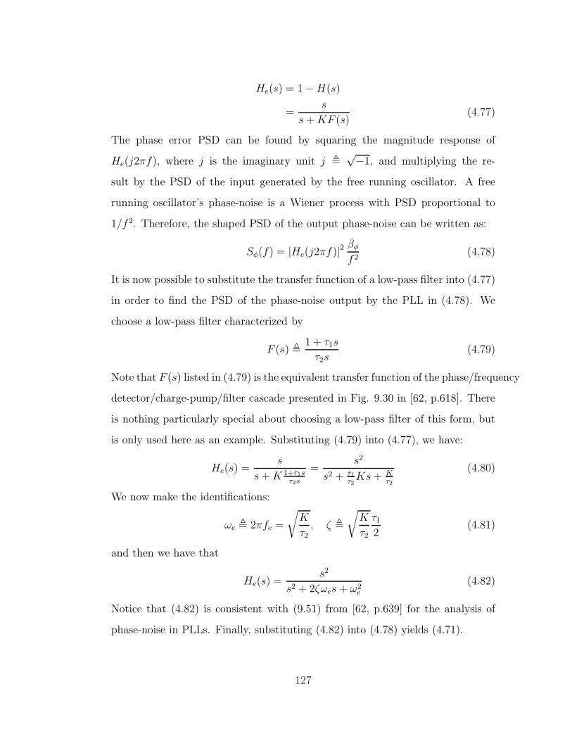
He(s) = 1−H(s)
=s
s+KF (s)(4.77)
The phase error PSD can be found by squaring the magnitude response of
He(j2πf), where j is the imaginary unit j ,√−1, and multiplying the re-
sult by the PSD of the input generated by the free running oscillator. A free
running oscillator’s phase-noise is a Wiener process with PSD proportional to
1/f 2. Therefore, the shaped PSD of the output phase-noise can be written as:
Sφ(f) = |He(j2πf)|2βφf 2
(4.78)
It is now possible to substitute the transfer function of a low-pass filter into (4.77)
in order to find the PSD of the phase-noise output by the PLL in (4.78). We
choose a low-pass filter characterized by
F (s) ,1 + τ1s
τ2s(4.79)
Note that F (s) listed in (4.79) is the equivalent transfer function of the phase/frequency
detector/charge-pump/filter cascade presented in Fig. 9.30 in [62, p.618]. There
is nothing particularly special about choosing a low-pass filter of this form, but
is only used here as an example. Substituting (4.79) into (4.77), we have:
He(s) =s
s+K 1+τ1sτ2s
=s2
s2 + τ1τ2Ks+ K
τ2
(4.80)
We now make the identifications:
ωe , 2πfe =
√
K
τ2, ζ ,
√
K
τ2
τ12
(4.81)
and then we have that
He(s) =s2
s2 + 2ζωes + ω2e
(4.82)
Notice that (4.82) is consistent with (9.51) from [62, p.639] for the analysis of
phase-noise in PLLs. Finally, substituting (4.82) into (4.78) yields (4.71).
127

4.C Effective signal-to-noise ratio (ESNR)
To illustrate why a training signal is useful, consider the estimation of the jitter
e[n] from the model
r[n] ≈ r[n] + e[n]r[n] + v[n] (4.83)
using linear least-mean-squares estimation techniques. Assume we collect data
samples of r[n] into a vector r and use the data to estimate the corresponding
vector of jitter samples, e. The linear least-mean-squares estimator of e given r
is given by the expression below in terms of the covariance matrix of r and the
cross-covariance matrix between e and r [42]:
e = RerR−1r r ≈ Rediag (Dr)R
−1r r (4.84)
where D is a differentiation matrix such as 12Ts
toeplitz[−1, 0, 1].
Note, however, from (4.83) that the jitter signal that we are interested in
recovering appears in the term e[n]r[n] and r[n] represents a strong interferer.
We can assess the power in e[n]r[n] relative to the other terms (which can be
treated as added disturbances in the problem of recovering e[n] from r[n]) by
defining the Effective-Signal-To-Noise-Ratio (ESNR) as
ESNR ,E[|e[n]r[n]|2
]
E |r[n]|2 + E |v[n]|2=
σ2eσ
2r
σ2r + σ2
v
(4.85)
The above expression can be bounded for a band-limited signal r[n] (having
frequencies up to Br) through the use of Parseval’s relation – see App. 4.F:
ESNR ≤ σ2e(2πBr)
2σ2r
σ2r + σ2
v
(4.86)
Observe that even when σ2v ≪ σ2
r , the ESNR is still bounded from above by
(2πγrα)2 where γr <
12is a factor that parameterizes the bandwidth of the signal
128

r[n] as Br = γrfs. For small jitter, such as 1% of Ts, the ESNR is bounded from
above by −30dB and is too small for effective estimation of e[n]. For this reason,
we pursue an alternative approach to recovering the jitter from the distorted
data r[n]. Rather than pursue a direct least-mean-squares estimation problem,
we instead inject auxiliary tones along with the input signal. By examining the
effect of the jitter on these embedded tones, we can then devise techniques to
estimate the jitter and compensate for it.
4.D Clock recovery
The jitter estimation algorithms of Sec. 4.2 require the recovery of the phase of
a sinusoid. This recovery can be done before the start of operations since the
phase of the injected tones does not depend on the incoming signal r[n]. Phase-
locked-loops can be used for this purpose [81, 88]. Consider a sequence of the
form x[n] = cos (2πfcnTs + θ), and introduce the objective function:
J(
θ)
= 2 · LPF
x[n] cos(2πfcnTs + θ)
= LPF
cos(θ − θ) + cos(4πfcnTs + 2θ)
≈ cos(θ − θ)
Thus, a steepest-ascent algorithm that maximizes J(θ) will force θ → θ:
dJ(
θ)
dθ
∣∣∣∣∣∣θ=θ(k)
= 2 · LPF
x[n]d
dθcos(
2πfcnTs + θ)∣∣∣∣θ=θ[n]
= 2 · LPF
−x[n] sin(
2πfcnTs + θ[n])
An adaptive update of the following form can be used to estimate θ recursively:
θ(n+ 1) = θ[n]− µLPF
x[n] sin(
2πfcnTs + θ[n])
(4.87)
129

Figure 4.15: Block diagram of the phase-locked-loop
Fig. 4.15 illustrates the algorithm. Other adaptive schemes can be constructed
in order to estimate θ [42].
4.E Power of N-th derivative of box-car random signal
In this appendix, we give an expression for the power of the N -th derivative of
a random signal r(t) with auto-correlation function given by (4.20). We assume
that the random process is mean-square integrable and that the auto-correlation
function of the derivative process can be computed using (4.15), which can be
extended to
Rr(N)(t)(τ) = (−1)Nd2N
dτ 2NRr(τ) (4.88)
where we use the notation r(N)(t) , dN
dtNr(t). It is possible to find E
∣∣ d
N
dtNr(t)|t=nTs
∣∣2
by finding the autocorrelation function of the discrete-time process and evaluating
it at lag m = 0. It is known that the autocorrelation function of the discrete-time
process dN
dtNr(t)
∣∣∣t=nTs
is the sampled autocorrelation function of the continuous-
time process dN
dtNr(t) given by Rr(N)(τ) [80]. This can be shown by considering a
continuous-time random process x(t) , dN
dtNr(t) with auto-correlation Rx(τ) and
the discrete-time process y[n] defined by y[n] , x(nTs). The auto-correlation
of the discrete-time process y[n] can be found as Ry(m) , E [y[n]y[n+m]] =
E [x(nTs)x(nTs +mTs)] = Rx(mTs). Thus, the two auto-correlation functions
coincide at m = 0 and it is sufficient to find the power of the continuous-time
130

process dN
dtNr(t). Moreover, we can compute the power in the derivative process
using:
σ2r(N) = Rr(N)(0) =
1
2π
∫ ∞
−∞Sr(N)(jΩ)dΩ
(a)=
(−1)N
2π
∫ ∞
−∞(jΩ)2NSr(jΩ)dΩ
=1
2π
∫ ∞
−∞Ω2NSr(jΩ)dΩ
where (a) is a consequence of (4.88). We now substitute in the PSD associ-
ated with the signal with auto-correlation (4.15) – thus we substitute Sr(jΩ) =
σ2r
2Brrect
(Ω
2π2Br
)
where rect(a) is defined in (4.19):
σ2r(N) =
1
2π
∫ ∞
−∞Ω2NSr(jΩ)dΩ
=σ2r
2π2Br
∫ 2πBr
−2πBr
Ω2NdΩ
=σ2r
2πBr
(2πBr)2N+1
2N + 1
=(2πBr)
2N
2N + 1σ2r
Thus, we conclude that
E
∣∣∣∣
dN
dtNr(t)
∣∣∣∣t=nTs
∣∣∣∣
2
=(2πBr)
2N
2N + 1σ2r (4.89)
4.F Bounding the power of the derivative of a random
signal
We bound the power of the derivative of a band-limited, zero mean, mean-square
differentiable WSS Gaussian random process r(t) with variance σ2r , autocorrela-
tion function Rr (τ), and PSD function Sr(jΩ). We define the continuous time
signal x(t) = dN
dtNr(t) with autocorrelation function Rx(τ). The auto-correlation
131

Rx(τ) can be found as an extension of (4.15) to be:
Rx(τ) = (−1)Nd2N
dτ 2NRr(τ) (4.90)
and PSD function Sx(jΩ):
σ2x = Rx (0)
(a)=
1
2π
∞∫
−∞
(−1)N(jΩ)2NSr (jΩ) dΩ
(b)
≤ (2πfmax)2N 1
2π
∞∫
−∞
Sr (jΩ) dΩ = (2πfmax)2N σ2
r
where (a) is a consequence of (4.15) and (b) is a consequence of r(t) being ban-
dlimited to fmax. Thus, we have shown σ2x ≤ (2πfmax)
2N σ2r .
We note that this power bound is still valid even for a sampled process y[n] ,
x(nTs) since the auto-correlation function of y[n] can be found as Ry(m) ,
E [y[n]y[n+m]] = E [x(nTs)x(nTs +mTs)] = Rx(mTs). Thus the two auto-
correlation functions coincide at m = 0 and it is sufficient to find the bound on
the power of the continuous-time process x(t) as we have done above.
132
CHAPTER 5
Compensating Mismatches in Time-Interleaved
A/D Converters
An M-channel time-interleaved analog-to-digital converter (ADC) uses M ADCs
to sample an input signal to obtain a larger effective sampling rate. However,
in practice, combining ADCs introduces mismatches between the various ADC
channels [68]. There is also the possibility of frequency response mismatches
[70,89–91]. Several techniques have been advanced in the literature to ameliorate
the effect of mismatches on the performance of time-interleaved ADC (TI-ADC)
implementations. For example, in [92, 93] a reference ADC is used alongside the
TI-ADC structure. In [94], the input signal is assumed to have some empty
frequency band and compensation for the mismatches is formulated in terms of a
nonlinear least-squares problem. In [95, 96], the timing and gain mismatches are
estimated by enforcing some empty frequency band constraints. In [1,15,97,98], it
is assumed that the distortions appear in an out-of-band region where no signal
components are present. In [99], the input signal is assumed to be sparse to
enhance estimation of the mismatch parameters.
While most of these prior works rely on exploiting the existence of some empty
frequency bands where no signal components occur, there are other works that
pursue alternative routes. In [14], the offset, gain, and timing errors are estimated
by optimizing certain loss functions. In [100, 101], an auto-correlation method is
133

used to detect and estimate timing errors. In [102–104], a two-step approach is
implemented. First, the timing mismatch is compensated for and the residual
error is computed by means of an approximate Hilbert filter. Subsequently, the
residual error is used to reduce the timing error. In [2], a pseudo aliasing signal
is generated using the Hadamard transform to compensate for the timing and
gain mismatches in the distorted signal. The distortion parameters are estimated
by re-generating the pseudo aliasing signal from the compensated signal and
correlating it with the compensated signal.
In this work, we propose two solutions for the compensation of time and gain
mismatches that eliminate some of the limitations of the existing approaches
[20, 21]. One solution technique is implemented in the time-domain and the
other solution technique is implemented in the frequency domain. The latter is
shown to have significantly superior performance. The time-domain approach
has some similarities with the solution methods of [1, 2] and therefore suffers
from similar limitations. We explain these difficulties in the body of the chapter.
In comparison, the frequency-domain approach addresses the limitations and is
able to deliver enhanced performance over existing methods, even under more
relaxed conditions. For example, the structure of reference [1] is based on one
key assumption: the input signal needs to be oversampled and an out-of-band
frequency region should be known beforehand where no signal components are
present. In this band, only contributions from the distortions caused by the
mistmatches are assumed to be present. By focusing on this region, adaptation
can be performed to reduce the effect of the distortions. However, it is not
uncommon for the conditions assumed by [1] to be violated. For instance, the
input signal may be wideband and the spectrum of the error signals may not be
limited to separate frequency regions that are free of signal contribution. When
these conditions occur, the solution of [1] fails. The time-domain approach of the
134

current chapter and that of [2] are able to address some of these limitations in
that they do not assume the pre-existence of an out-of-band region. While this
is an advantage, it nevertheless degrades the performance of the solution relative
to [1] when an out-of-band region happens to be present.
The frequency-domain approach removes this drawback altogether because it
employs a structure that is able to automatically locate and exploit out-of-band
regions when they are present. In this approach, we transform the data into the
frequency domain by means of an N−point FFT operation. The data across
each FFT channel then amounts to data around a certain frequency bin. In this
way, the frequency space is sliced into N adjacent frequency bins. Adaptation is
performed over each channel to estimate the mismatch parameters. By tracking
the signal power over the various channels, the structure is able to learn which
channels have more or less reliable estimates of the mismatch parameters. These
estimates are then fused using an adaptive strategy [42] to obtain an enhanced
final estimate for the parameters. The frequency-domain approach can therefore
adapt to the input signal; it has accelerated convergence and comparable perfor-
mance to [1] when the input signal contains known empty frequency bands, and
is still able to mitigate the timing and gain mismatches in cases where [1] cannot,
including situations when the input signal contains unknown empty frequency
bands or does not contain any empty frequency band.
There are additional advantages for the frequency-domain structure. Adap-
tation is performed across each channel to estimate the parameter mistmatches.
Interference cancelation by means of such adaptive constructions is aided by an
implicit assumption of uncorrelatedness between the signal and the interference.
There are a couple of steps in the frequency-domain implementation that help
reduce the effect of correlation between the signal and the interference; (a) first,
135

data are processed in the frequency domain and not in the time domain. By means
of the FFT, the signal is split into small frequency bands. Over these smaller
bands, the signal component and the interference component are generally more
likely to be uncorrelated with each other [105,106]; (b) second, the solution com-
bines the estimates of the mismatch parameters from across all channels and the
combination weights are chosen in a manner that gives more relevance to esti-
mates arising from bands where there is less frequency overlap between signal
and interference (and, hence, less correlation); (c) third, the frequency structure
employs a succession of two adaptation stages; the second stage exploits any
correlation that is left in the data after processing by the first stage in order
to further enhance the estimation accuracy of the mismatch parameters. The
analysis and simulations illustrate the superior performance of this construction.
5.1 Problem formulation
The structure of the TI-ADC model in the presence of imperfections across the
multiple ADC branches is already well-presented in the literature (see, e.g., [1,
68]). We briefly review the model here. Figure 5.1 shows the block diagram
representation of an M-channel TI-ADC with gain and timing mismatches. Let
us denote the gain and timing mismatches in the m-th channel by gm and rmTs,
where rm represents the timing mismatch relative to the overall sampling period
Ts. The input signal x(t) is spilt into M channels and the m−th branch is
multiplied by gm and sampled at (ℓM+m+rm)Ts; the resulting sequence is zm[ℓ].
A multiplexer (MUX) is used to combine the sampled data from all channels into
the output sequence y[n]. The effective sampling period for y[n] is seen to be Ts.
In the ideal scenario, where the ADCs are perfect data converters, gm and rm
will be 1 and 0, respectively.
136

Figure 5.1: The figure shows an M -Channel TI-ADC with linear mismatches (gain and
timing).
From [1], it is already known that the discrete-time Fourier transform (DTFT)
of the sequence y[n] can be expressed as
Y (ejω) =
M−1∑
k=0
X(
ej(ω−2πkM
))
Hk
(
ej(ω−2πkM
))
(5.1)
where X(ejω) is the DTFT of the sampled sequence x[n] = x(t)|nTsand
Hk
(ejω)=
1
M
M−1∑
m=0
gmermHd(e
jω)e−jk 2πM
m (5.2a)
Hd
(ejω)= jω, for − π < ω ≤ π (5.2b)
The derivation is shown in Section 5.B. It is clear from (5.1) that when the
TI-ADC has mismatches, the output spectrum contains the original spectrum
X(ejω) multiplied by H0(ejω), and frequency-shifted versions of the product
X(ejω)Hk(ejω). Figure 5.2 illustrates the spectrum of the distorted output se-
quence of the TI-ADC for M = 2, 4. The figure shows the magnitude DTFT
of the input sequence (represented by the black triangular curve centered at 0)
and the magnitude DTFTs of the interfering error signals (represented by the
remaining triangular curves).
137

Figure 5.2: The figure shows the spectrum Y (ejω) of the TI-ADC for M = 2, 4. The
black triangle centered at 0 is the spectrum X(ejω)H0(ejω) and the remaining triangles
represent the interfering error spectra generated by the mismatches. Each frequency-
shifted spectrum X(ejω)Hk(ejω) has a different color.
5.2 Existing techniques and limitations
As already remarked in the introduction, there have been several efforts in the
literature to address the TI-ADC compensation problem with varied degrees of
success and often under varying assumptions on the nature of the data. One
useful approach is proposed in [1] and appears to lead to the best performance
among existing techniques (when its assumptions hold). To facilitate comparison
with [1], we review briefly its main contribution (using our notation) and comment
on some of the limitations of the approach before moving on to develop the
solution method of this work.
5.2.1 Linear approximation
Reference [1] assumes the timing mismatches rm are small and assumes a first-
order Taylor’s series approximation can be applied to the term ermHd(ejω) in (5.2a)
138
as
ermHd(ejω) ≈ 1 + rmHd(e
jω) (5.3)
Substituting (5.3) into (5.2a) gives
Hk
(ejω)≈ Gk +RkHd(e
jω) (5.4)
where
Gk =1
M
M−1∑
m=0
gme−j 2π
Mmk (5.5a)
Rk =1
M
M−1∑
m=0
gmrme−j 2π
Mmk (5.5b)
The variables Gk, Rk contain information about the gain and delay mismatches
across the branches. Observe that Go =1M
∑M−1m=0 gm represents the average gain
mismatch across all channels. It can be assumed, without loss of generality,
that the average value of the timing mismatches is zero, i.e., 1M
∑M−1m=0 rm ≈ 0.
Reference [1] further assumes that R0 is small and can be neglected. Under
these conditions, the inverse discrete-time Fourier transform (IDTFT) of (5.1) is
derived
y[n] = G0x[n] + e[n] (5.6)
where all interfering terms are collected into the error signal, e[n]. It is shown
in [1] that, when M is even, the error e[n] can be expressed as the sum of two
inner-product components:
e[n] = cTg xg,n + cTr xr,n (5.7)
where the vectors xg,n and xr,n contain modulated samples of the signal x[n] and
its “derivative” version hd[n] ⋆ x[n]. Specifically, the notation hd[n] denotes the
139
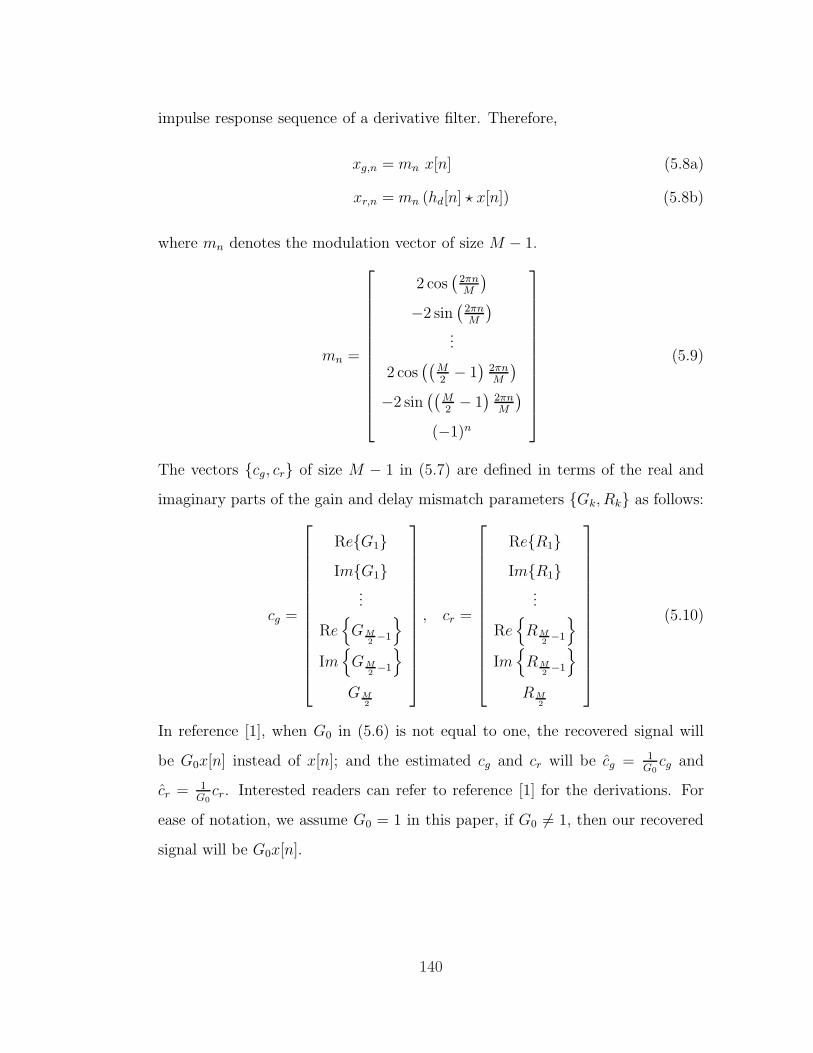
impulse response sequence of a derivative filter. Therefore,
xg,n = mn x[n] (5.8a)
xr,n = mn (hd[n] ⋆ x[n]) (5.8b)
where mn denotes the modulation vector of size M − 1.
mn =
2 cos(2πnM
)
−2 sin(2πnM
)
...
2 cos((
M2− 1)
2πnM
)
−2 sin((
M2− 1)
2πnM
)
(−1)n
(5.9)
The vectors cg, cr of size M − 1 in (5.7) are defined in terms of the real and
imaginary parts of the gain and delay mismatch parameters Gk, Rk as follows:
cg =
ReG1ImG1
...
Re
GM2−1
Im
GM2−1
GM2
, cr =
ReR1ImR1
...
Re
RM2−1
Im
RM2−1
RM2
(5.10)
In reference [1], when G0 in (5.6) is not equal to one, the recovered signal will
be G0x[n] instead of x[n]; and the estimated cg and cr will be cg = 1G0cg and
cr = 1G0cr. Interested readers can refer to reference [1] for the derivations. For
ease of notation, we assume G0 = 1 in this paper, if G0 6= 1, then our recovered
signal will be G0x[n].
140

5.2.2 Compensation
The challenge is to recover the samples x[n] in (5.6) from knowledge of y[n].
The error component e[n] in (5.6) is not known because it depends on unknown
gain and delay mismatch parameters. Reference [1] replaces x[n] by y[n] on the
right-hand side of (5.8) and uses the following expression to estimate e[n]:
e[n] = cTg,n−1mny[n] + cTr,n−1mn (hd[n] ∗ y[n]) (5.11)
where cg and cr are estimates for the vectors cg and cr, respectively; these esti-
mates are computed as explained further ahead. Using (5.11), then
y[n]− e[n] ≈ x[n] (5.12)
This construction leads to the compensation structure shown in Fig. 5.3.
Figure 5.3: The figure shows the compensation and identification structure used in
reference [1].
In order to estimate the vectors cg, cr, reference [1] assumes that the input
signal is a low-pass signal and that the TI-ADC oversamples the signal. In this
141

way, an empty frequency band in higher frequencies will become available that is
free of signal content. This frequency band will only contain contributions that
arise from the error spectra due to the gain and delay mismatches. This situation
is illustrated in Fig. 5.4 for M = 2, 4. As such, reference [1] uses a high-pass
Figure 5.4: The figure shows the spectrum of the TI-ADC for M = 2, 4 when the input
signal is oversampled. The black triangle centered at 0 is the spectrum of the original
signal x[n], and the remaining triangles represent the error spectra generated by the
mismatches. Note that the original spectrum does not cover the entire band from −π
to π. Hence, there is an out-of-band region that contains only error spectra.
filter f [n] to remove the input signal and concentrates on estimating the vectors
cr, cg in order to reduce the distortion that is present in the out-of-band region.
The LMS algorithm [42] is used to estimate the parameters cg and cr as follows.
Referring to Fig. 5.3, the estimated error signal, e[n] is high-pass filtered by f [n]
and used to generate an error component ǫ[n] to drive the adaptation process.
The estimated vectors xg,n and xr,n are also filtered through f [n] to generate
xg,n, xr,n. These quantities are then used in adapting cr,n, cr,n:
cg,n = cg,n−1 + µxTg,nǫ[n] (5.13a)
cr,n = cr,n−1 + µxTr,nǫ[n] (5.13b)
142
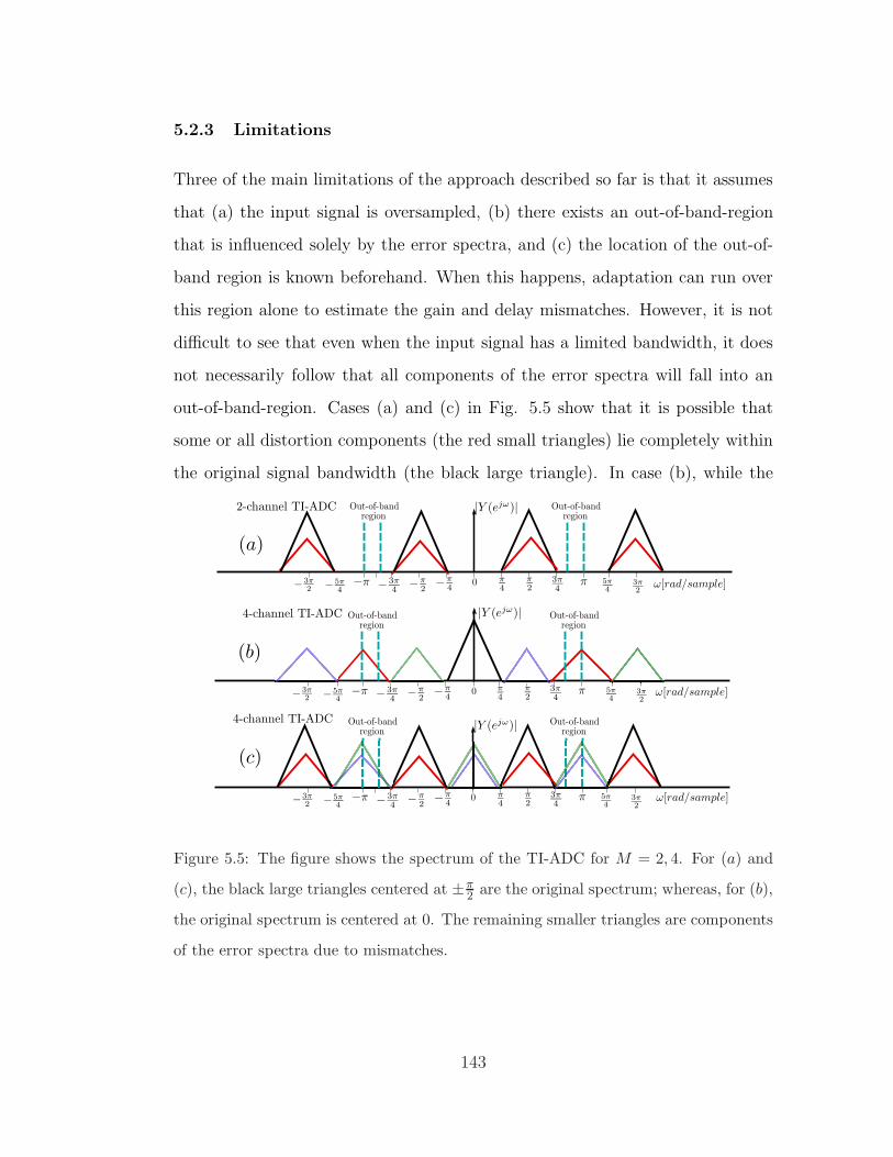
5.2.3 Limitations
Three of the main limitations of the approach described so far is that it assumes
that (a) the input signal is oversampled, (b) there exists an out-of-band-region
that is influenced solely by the error spectra, and (c) the location of the out-of-
band region is known beforehand. When this happens, adaptation can run over
this region alone to estimate the gain and delay mismatches. However, it is not
difficult to see that even when the input signal has a limited bandwidth, it does
not necessarily follow that all components of the error spectra will fall into an
out-of-band-region. Cases (a) and (c) in Fig. 5.5 show that it is possible that
some or all distortion components (the red small triangles) lie completely within
the original signal bandwidth (the black large triangle). In case (b), while the
Figure 5.5: The figure shows the spectrum of the TI-ADC for M = 2, 4. For (a) and
(c), the black large triangles centered at ±π2 are the original spectrum; whereas, for (b),
the original spectrum is centered at 0. The remaining smaller triangles are components
of the error spectra due to mismatches.
143

error components do not interfere with the signal bandwidth, only part of them
lie within the out-of-band region. In these scenarios, the algorithm of [1] will not
be able to remove the distortions and recover the desired signal. The techniques
proposed in the current work do not have these limitations. In particular, they
do not rely on the use of any out-of-band region for adaptation. This is achieved
by processing data in the frequency domain and by using adaptation strategies
to combine information from across frequency bins to carry out the desired com-
pensation. When an out-of-band region exists, we will see that our proposed
method performs similarly to [1]. When an out-of-band region does not exist,
our proposed method will continue to perform well while the method of [1] will
not be suitable for such situations.
5.3 Proposed solutions
Two solutions are proposed in this section. One solution is in the time-domain
and is able to address more scenarios than described so far. The second solution
is in the frequency domain and leads to superior performance.
5.3.1 Time-domain solution
Using (5.6) and (5.7), we can write
y[n] =[
xTg,n xTr,n
]
︸ ︷︷ ︸
,uTn
cg
cr
︸ ︷︷ ︸
,wo
+ x[n] (5.14a)
= uTnwo + x[n] (5.14b)
which expresses the output signal y[n] as the sum of two components: the desired
clean signal, x[n], and the linear regression term, uTnwo. We now refer to the basic
144

structure for adaptive interference cancelation shown in Fig. 5.6. In traditional
Figure 5.6: An adaptive structure for interference cancelation.
adaptive filtering, it is customary for the term x[n] to represent the noise com-
ponent when we estimate wo. In the current setting, though, x[n] represents the
signal component that we wish to estimate and retain. This can be accomplished
by using LMS adaptation to estimate wo from knowledge of y[n], un (5.14):
wn = wn−1 + µuTn(y[n]− uTnwn−1) (5.15)
The main challenge in running this algorithm is the need to know the regression
data un; this data depends on the vectors xg,n, xr,n, which in turn depend on
the unknown signal x[n]. In the sequel, we present two methods for estimating
these quantities and replacing un by
un =[
xTg,n xTr,n
]T
(5.16)
We first describe a time-domain solution. We again substitute x[n] by y[n] in
(5.8) to approximate the vectors xg,n, xr,n by
xA,g,n = mny[n], xA,r,n = mn(hd[n] ∗ y[n]) (5.17)
This is the same approximation that was employed earlier in (5.11). Due to the
approximation, the estimate for x(n) that results from this approximation in Fig.
145

5.6 can be refined further. We denote the initial estimate by xA[n] in the left-
part of Fig. 5.7. We then use it to feed another similar interference cancelation
structure to refine it into xB[n]. The net effect is the cascade structure shown in
Fig. 5.7. We will illustrate the performance of this mechanism in a later section.
We move on to describe the second solution method, which is in the frequency
domain.
Figure 5.7: Block diagram representation of the proposed time-domain solution.
Figure 5.8: Block diagram representation of the frequency-domain solution based on a
first-order compensation stage, where Hd[k] is defined in (5.19).
146

5.3.2 Frequency-domain solution
The time-domain solution removes the limitations of the previous work. However,
it ignores the possibility that the input signal may contain out-of-band regions
with only distortion components and that these regions could be exploited for
additional enhancements. This observation motivates an alternative approach
where data are processed in the frequency domain. By partitioning the data
spectrum into smaller frequency bands, it becomes possible to search the fre-
quency content of these bands to detect the existence of out-of-band regions.
The frequency-domain approach assesses the relevance of the various frequency
bands to the estimation task and this information is shared across the frequency
domain filters. Through an adaptive process, the information is aggregated and
exploited to assign more or less relevance to bands that carry more or less infor-
mation about signal content and error content. Bands that help reduce the error
components are given more weight to drive the adaptation process more steadily
towards its aim. Since signals and their frequency contents can change over time,
the adaptive process is able to evolve and track these variations continuously.
The block diagram of the frequency-domain approach is shown in Fig. 5.8.
A block of data of size N is collected and windowed before undergoing an FFT
transformation of size N . This step results in N bins denoted by Yi[k] ≈ Xi[k] +
Ei[k], for k = 0, 1, . . . , N − 1. The subscript i is used to denote successive
blocks of data. For each frequency bin, we employ a structure similar to Fig.
5.7 consisting of a compensation block followed by a cancellation block. The
compensation block is used to estimate the first order error Ei[k] and to generate
an initial estimate for Xi[k] (denoted by XA1,i[k]). This information is then fed
into a subsequent cancellation block to generate XB,i[k]. In the model shown
in Fig. 5.8 we are including an additional noise variable, denoted by vnoise[n] in
147
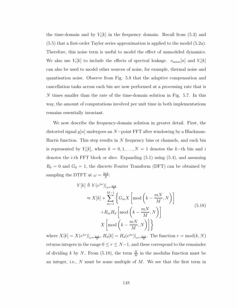
the time-domain and by Vi[k] in the frequency domain. Recall from (5.3) and
(5.5) that a first-order Taylor series approximation is applied to the model (5.2a).
Therefore, this noise term is useful to model the effect of unmodeled dynamics.
We also use Vi[k] to include the effects of spectral leakage. vnoise[n] and Vi[k]
can also be used to model other sources of noise, for example, thermal noise and
quantisation noise. Observe from Fig. 5.8 that the adaptive compensation and
cancellation tasks across each bin are now performed at a processing rate that is
N times smaller than the rate of the time-domain solution in Fig. 5.7. In this
way, the amount of computations involved per unit time in both implementations
remains essentially invariant.
We now describe the frequency-domain solution in greater detail. First, the
distorted signal y[n] undergoes an N−point FFT after windowing by a Blackman-
Harris function. This step results in N frequency bins or channels, and each bin
is represented by Yi[k], where k = 0, 1, . . . , N = 1 denotes the k−th bin and i
denotes the i-th FFT block or slice. Expanding (5.1) using (5.4), and assuming
R0 = 0 and G0 = 1, the discrete Fourier Transform (DFT) can be obtained by
sampling the DTFT at ω = 2πkN:
Y [k] , Y (ejω)|ω= 2πkN
≈ X [k] +M−1∑
m=1
GmX
[
mod
(
k − mN
M,N
)]
+RmHd
[
mod
(
k − mN
M,N
)]
X
[
mod
(
k − mN
M,N
)]
(5.18)
where X [k] = X(ejω)|ω= 2πkN, Hd[k] = Hd(e
jω)|ω= 2πkN. The function r = mod(k,N)
returns integers in the range 0 ≤ r ≤ N−1, and these correspond to the remainder
of dividing k by N . From (5.18), the term NM
in the modulus function must be
an integer, i.e., N must be some multiple of M . We see that the first term in
148

(5.18) is the original signal and the terms in the summation are the distortions.
In (5.18), multiplying Hd[k] with X [k] can be interpreted as finding the discrete-
time derivative of the time-domain signal by modeling the time-domain signal
as a trigonometry polynomial and applying a spectral differentiation approach
in [107, p. 23]. Using (5.2b), Hd[k] is given by:
Hd[k] =
j 2πkN
if 0 ≤ k ≤ N2− 1
0 if k = N2
j 2π(k−N)N
if N2+ 1 ≤ k ≤ N − 1.
(5.19)
Note that Hd[k] has the conjugate symmetry property Hd[k] = (Hd[N − k])∗.
Using (5.18), we can write Yi[k] as
Yi[k] = Xi[k] + Ei[k] + Vi[k] (5.20)
where Xi[k] represents the output when the original signal x[n] goes through
the N -FFT block with the same windowing function, Ei[k] represents first-order
distortion terms, and Vi[k] contains the spectral leakage due to windowing, un-
modeled higher-order dynamics and other sources of system noise like thermal
noise and quantization noise. We can express Ei[k] compactly as follows: Firstly,
we define the differentiation operator Xi[ℓ] on the block of data (for example, on
a block of Xi[ℓ], ℓ = 0, ..., N − 1) as
Xi[k] , Hd[k]Xi [k] (5.21)
where Hd[k] is defined in (5.19). Secondly, we let
αk,m , mod
(
k − (m+ 1)N
M,N
)
(5.22)
Next, we define the following vectors:
Xgk,i ,
[
Xi [αk,0] ... Xi [αk,M−2]]T
(5.23a)
Xrk,i ,
[
Xi [αk,0] ... Xi [αk,M−2]]T
(5.23b)
149

We can interpret each element in the vectors Xgk,i and X
rk,i as a circular shift of
Xi[k] and Xi[k] by multiples of NM. Hence, we can write Ei[k] in (5.20) as
Ei[k] =(Xg
k,i
)TCG +
(Xr
k,i
)TCR (5.24a)
CG =[
G1 G2 ... GM−1
]T
(5.24b)
CR =[
R1 R2 ... RM−1
]T
(5.24c)
Using (5.24), the compensation block (labeled as Stage A1) in Fig. 5.8 esti-
mates the first-order distortion EA1,i[k] and subtracts it from Yi[k] to obtain an
estimate for the original signal, XA1,i[k]:
XA1,i[k] = Yi[k]− EA1,i[k] (5.25)
Similar to the time-domain approach, the distortion EA1,i[k] is approximated
using Y [k] in place of X [k] in (5.24) as
EA1,i[k] =(
XgA1,k,i
)T
CG,i−1 +(
XrA1,k,i
)T
CR,i−1 (5.26)
where XgA1,k,i and X
rA1,k,i are obtained from (5.21) and (5.23) by replacing Xi[·]
by Yi[·].
XgA1,k,i ,
[
Yi [αk,0] ... Yi [αk,M−2]]T
(5.27a)
XrA1,k,i ,
[
Yi [αk,0] ... Yi [αk,M−2]]T
(5.27b)
The terms CG,i−1 and CR,i−1 are estimates for the vectors Cg and Cr computed at
the (i − 1)−th iteration in a manner described further ahead. In the next stage
(labeled as stage B: interference cancelation) in Fig. 5.8, the estimated regressors
XgB,k,i and X
rB,k,i are generated in a similar manner as Xg
A1,k,i and XrA1,k,i in the
first stage. They are obtained from (5.21) and (5.23) by replacing Xi[·] by XA1,i[·].The output from stage B is the recovered signal XB,i[k]:
XB,i[k] = Yi[k]− EB,i[k] (5.28)
150

where EB,i[k] is obtained in a similar manner as (5.26), where we replace XgA1,k,i
and XrA1,k,i by X
gB,k,i and X
rB,k,i, respectively.
EB,i[k] =(
XgB,k,i
)T
CG,i−1 +(
XrB,k,i
)T
CR,i−1 (5.29)
We explain further ahead how the regressors XgB,k,i and X
rB,k,i are used to estimate
CG,i and CR,i from Yi[k] — see (5.33) and (5.34).
We now describe the details of the adaptation process and how estimates
from across different frequency bins are aggregated. We do so by explaining
the analogy with adaptive networks where nodes cooperate with their neighbors
to improve their estimates [108–110]. Adaptive networks deal generally with
arbitrary topologies linking their nodes. In the context of the current problem,
each bin plays the role of an agent and its neighbors are the remaining bins, i.e., in
this case, it is sufficient to assume that we have a fully connected mesh topology
as shown in Fig. 5.9. The adaptation process is described as follows. We adjust
Figure 5.9: Mesh network representing the interactions among all N frequency bins for
k = 0, 1, . . . , N − 1.
the notation to emphasize the role that is played by the different frequency bins.
We now denote Yi[k] in (5.20) by Dk[i], with the subscript k emphasizing that
151

we are now examining data collected over time at bin k. We then observe that
we can rewrite the data model for the k−th node (or bin) in the i−th FFT block
as:
Dk[i] , Yi[k] = Ei[k] +Xi[k] + Vi[k]︸ ︷︷ ︸
Zk[i]
= Uk,iWo +Zk[i] (5.30)
The linear regression, Uk,iWo, is the mismatch distortion, Ei[k]. Moreover, Xi[k]
and Vi[k] are combined together as Zk[i]. We assume that Vi[k] is small relative
to Xi[k], therefore Zk[i] ≈ Xi[k]. Hence, if the distortion Ei[k] = Uk,iWo is
estimated correctly and removed from Yi[k], we can recover our desired signal
Xi[k] at the output of Stage B. From (5.24), we collect the entries of CR, CGinto the column vector W o, and Xg
k,i, Xrk,i into the regression row vector Uk,i,
namely,
Uk,i =[
U ak,i[0] ... U a
k,i[M − 2]]
(5.31a)
W o =[
W a,o[0] ... W a,o[M − 2]]T
(5.31b)
where the row sub-vector U ak,i[m] and column sub-vectorsW a,o[m] are constructed
as:
U ak,i[m] =
[
Xgk,i[m] Xr
k,i[m]]
(5.32a)
W a,o[m] =[
CG[m] CR[m]]T
(5.32b)
The sub-vectors W a,o[m] are expressed in this manner since we will linearly com-
bine the intermediate sub-vectors ψaℓ,i[m] to estimate W a,o[m] in the next step
(see (5.33b) and (5.33c)). Each bin k now uses its own data Dk[i],Uk,i, arisingfrom the k-th frequency bin, and estimates from the other nodes arising from data
152

in their frequency bins, to estimate W o in the following cooperative manner:
ψk,i =Wk,i−1 + µk,iU∗k,i (Dk[i]−Uk,iWk,i−1) (5.33a)
ψak,i[m] =
[
ψk,i[2m] ψk,i[2m+ 1]]T
(5.33b)
W ak,i[m]=
N−1∑
ℓ=0
aℓ,k,i[m]ψaℓ,i[m] (5.33c)
Wk,i =[(W a
k,i[0])T
...(W a
k,i[M − 2])T]T
(5.33d)
where m = 0, ...,M − 2. Similar to the time-domain approach, and since we
do not have the actual Uk,i, we use the estimated regressors XgB,k,i and X
rB,k,i:
Uk,i ≈[
U ak,i[0] ... U a
k,i[M − 2]]
(5.34a)
U ak,i[m] =
[
XgB,k,i[m] Xr
B,k,i[m]]
(5.34b)
During the first step of the implementation in (5.33a), the k-th bin (or node)
starts from its existing vector estimateWk,i−1 and updates it to an intermediate
value ψk,i using solely data from its frequency bin. All other bins are performing a
similar operation and updating their estimates,Wℓ,i−1, to the intermediate values
ψℓ,i. In the remaining steps of (5.33), the k−th bin combines in a convex manner
the intermediate estimates of all other bins to obtain the sub-vector, W ak,i[m], of
its updated weight vectorWk,i. The scalar coefficients aℓ,k,i[m] are nonnegative
values that add up to one; observe that they are allowed to vary with the iteration
index i since we are going to select these weights adaptively as well. Each weight
aℓ,k,i[m] can be interpreted as the amount of trust that bin k places on the weight
estimate from bin ℓ at iteration i. Since some bins may correspond to frequency
bands that are better suited for the compensation task (such as bands that only
contain error spectra), then by allowing the algorithm to identify these bands on
the fly and to adjust the combination coefficients aℓ,k,i[m] in real-time, more
or less weight can be assigned to the data from bin ℓ depending on whether the
153

data is deemed to be more or less relevant to the estimation task. We explain in
the sequel how these combination weights are adapted.
Recall that the adaptive algorithm (5.33) is estimating the distortion param-
eter W o in (5.30). Moreover, from (5.30), we see that we are estimating W o from
Uk,iWo under the presence of Zk[i]. In this context, we see that if the magnitude
of Uk,i and Zk[i] is large and small, respectively, the intermediate estimate ψk,i
should be estimated more accurately. Hence, we would like to find a measure that
emphasizes the estimates that originate from bins that have better accuracy. For
this purpose, we first define the average power of the signals Zk[i] and Zk[i] as:
average power of Zk[i] , PZ [k] (5.35a)
average power of Zk[i] , PZ [k] = |Hd[k]|2 PZ [k] (5.35b)
Next, we quantify the average power of each element in Uk,i. From (5.31a) and
(5.32a), we see that Uk,i contains Xi[k] and Xi[k], which are circularly shifted by
αk.m. We approximate the average power of Xi[k] and Xi[k] by PZ [k] and PZ [k],
respectively. Then, we can express the average power of each element in Uk,i as
the vector PU,k:
PU,k ,[
P gk [0]P
rk [0]...P
gk [M − 2]P r
k [M − 2]]
(5.36a)
P gk ≈
[
PZ [αk,0] ... PZ [αk,M−2]]T
(5.36b)
P rk ≈
[
PZ [αk,0] ... PZ [αk,M−2]]T
(5.36c)
We define our initial measure of the power of the regressor components, P gk [m]
and P rk [m], versus the power of Zk[i], PZ [k], as the ratio:
PR,k[m] =P gk [m] + P r
k [m]
PZ [k](5.37)
Using a low-pass input signal as an illustration, we now explain the general form
of PR,k[m] looks like, and why it is problematic to rely on PR,k[m] alone as a
154
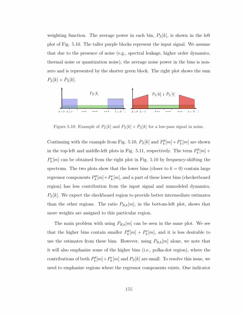
weighting function. The average power in each bin, PZ [k], is shown in the left
plot of Fig. 5.10. The taller purple blocks represent the input signal. We assume
that due to the presence of noise (e.g., spectral leakage, higher order dynamics,
thermal noise or quantization noise), the average noise power in the bins is non-
zero and is represented by the shorter green block. The right plot shows the sum
PZ [k] + PZ [k].
Figure 5.10: Example of PZ [k] and PZ [k] + PZ [k] for a low-pass signal in noise.
Continuing with the example from Fig. 5.10, PZ [k] and Pgk [m]+P r
k [m] are shown
in the top-left and middle-left plots in Fig. 5.11, respectively. The term P gk [m] +
P rk [m] can be obtained from the right plot in Fig. 5.10 by frequency-shifting the
spectrum. The two plots show that the lower bins (closer to k = 0) contain large
regressor components P gk [m]+P r
k [m], and a part of these lower bins (checkerboard
region) has less contribution from the input signal and unmodeled dynamics,
PZ [k]. We expect the checkboard region to provide better intermediate estimates
than the other regions. The ratio PR,k[m], in the bottom-left plot, shows that
more weights are assigned to this particular region.
The main problem with using PR,k[m] can be seen in the same plot. We see
that the higher bins contain smaller P gk [m] + P r
k [m], and it is less desirable to
use the estimates from these bins. However, using PR,k[m] alone, we note that
it will also emphasize some of the higher bins (i.e., polka-dot region), where the
contributions of both P gk [m]+P r
k [m] and PZ [k] are small. To resolve this issue, we
need to emphasize regions where the regressor components exists. One indicator
155

Figure 5.11: Illustration for the motivation behind the the proposed combination
weights.
is P gk [m], which is obtained by frequency-shifting PZ [k]. Therefore, the new
measure is the product PR,k[m]P gk [m]. The top, middle and bottom plots in the
right column of Fig. 5.11 show P gk [m], PR,k[m] and PR,k[m]P g
k [m], respectively.
Using (5.36b) and (5.37), the combination weight is set as
aℓ,k[m] =PR,ℓ[m]P g
ℓ [m]∑N−1
n=0 (PR,n[m]P gn [m])
(5.38)
where m = 0, ...,M − 2. The division operations can be implemented using
look-up-table (LUT) or CORDIC algorithms [111]. Observe that aℓ,k[m] is in
terms of PZ [k], which we do not know. One way to estimate it is [112]:
PZ,i[k] =
∣∣∣XB,i[k]
∣∣∣
2
if i = 0
λPZ,i−1[k] + (1− λ)∣∣∣XB,i[k]
∣∣∣
2
if i > 0
(5.39)
where λ is a forgetting factor close to one (say, λ = 0.95), and XB,i[k] is the
recovered signal at the output of stage B in Fig. 5.8. Since we are using (5.39) in
156

(5.38) in each iteration, we denote the adaptive combination weight as aℓ,k,i[m],
where we include the index i.
Observe that the combination weights in (5.38) computed in this manner
are independent of k. With reference to (5.33c), this property means that after
combining the intermediate estimates ψak,i[m], the estimated sub-vector W a
k,i[m]
for the k-th bin is the same for the sub-vector W aℓ,i[m] for all other bins, i.e.,
W ak,i[m] = W a
ℓ,i[m], ℓ = 0, ..., N − 1. Therefore, instead of updating Wk,i at
every node, we can update it once as Wi. As such, we will drop the index k
from aℓ,k,i,Wak,i[m], andWk,i[m] in (5.33). This configuration is analogous to the
intermediate estimates being fused centrally to determine the aggregate estimate.
In some situations, it may be known that some bins or nodes do not have any
signal content, in that case it is possible to set their weights to zero and remove
them from the aggregation step.
Now, we are left with the stepsize µk,i in (5.33a). The step-size needs to be
sufficiently small to ensure the mean stability of the adaptation process. This
can be assessed as follows (the justification is delayed to Appendix 5.A where
we establish condition (5.95) further ahead). For now, we remark the following.
We denote the covariance matrix of the regression vector Uk,i (assumed to be
wide-sense stationary and zero-mean) by:
RU,k , E[U ∗
k,iUk,i
](5.40)
We also denote the m-th non-zero eigenvalue of RU,k by λm (RU,k). Further ahead
in (5.62), we will show that RU,k has a block diagonal matrix structure, and each
block is a rank-1 matrix. Hence, RU,k is positive semi-definite. The non-zero
eigenvalue of each such rank-1 matrix is equal to its trace. Therefore, from
157

(5.36), each eigenvalue is
λm (RU,k) = P gk [m] + P r
k [m] (5.41)
The stepsize µk,i has to be bounded using the reciprocal of the maximum eigen-
value. Specifically, let
λmax (RU,k) = max λ0 (RU,k) , ..., λM−2 (RU,k) (5.42)
Then, for mean stability, it must hold that
µk,i ≤2
λmax (RU,k)(5.43)
Furthermore, recall from (5.30) that each bin is estimating W o from Uk,iWo in
the presence of Zk[i]. In this sense, Zk[i] is a noisy component in the estimation.
The average power of Zk[i] is defined in (5.35) as PZ [k]. Since, PZ [k] generally
differs across the bins, we are motivated to use a larger or smaller stepsize for bins
that have less or more noise power, respectively. One way to do so is to set the
stepsizes to be inversely proportional to PZ [k]. Together with (5.43), the stepsize
µk,i for the k-th node is then selected to be sufficiently small and to satisfy:
µk,i = β ·min
µinit
PZ [k],
2
λmax (RU,k)
(5.44a)
β ≤ 1 (5.44b)
where µinit is some fixed constant. Again, note that µk,i and λmax (RU,k) are in
terms of PZ [k]. Therefore, similar to the combination weights, we use (5.39) in
(5.44) to set µk,i. A summary of the steps is shown in Algorithm 5.1.
5.3.3 Enhanced frequency-domain solution
Before proceeding to analyzing the performance of the frequency-domain solution,
we first highlight two sources of higher-order approximation errors that have been
158
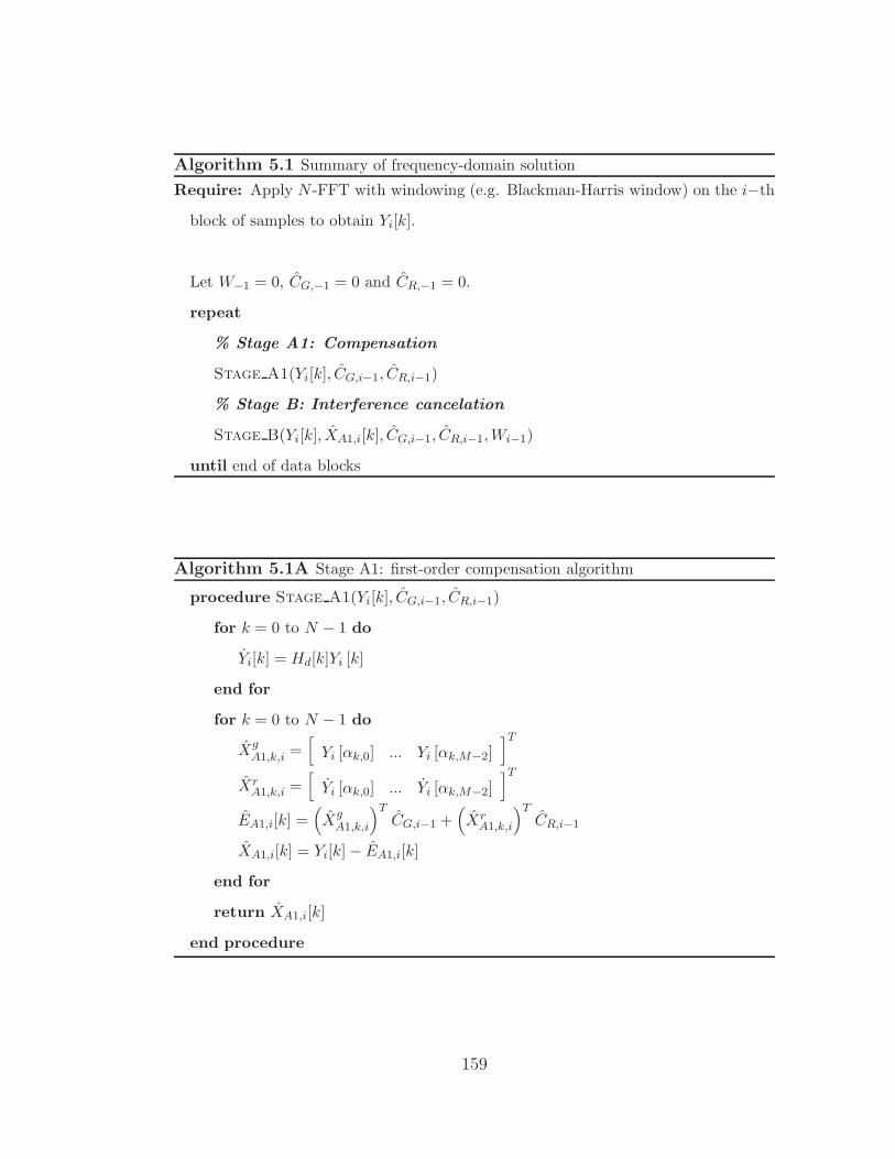
Algorithm 5.1 Summary of frequency-domain solution
Require: Apply N -FFT with windowing (e.g. Blackman-Harris window) on the i−th
block of samples to obtain Yi[k].
Let W−1 = 0, CG,−1 = 0 and CR,−1 = 0.
repeat
% Stage A1: Compensation
Stage A1(Yi[k], CG,i−1, CR,i−1)
% Stage B: Interference cancelation
Stage B(Yi[k], XA1,i[k], CG,i−1, CR,i−1,Wi−1)
until end of data blocks
Algorithm 5.1A Stage A1: first-order compensation algorithm
procedure Stage A1(Yi[k], CG,i−1, CR,i−1)
for k = 0 to N − 1 do
Yi[k] = Hd[k]Yi [k]
end for
for k = 0 to N − 1 do
XgA1,k,i =
[
Yi [αk,0] ... Yi [αk,M−2]]T
XrA1,k,i =
[
Yi [αk,0] ... Yi [αk,M−2]]T
EA1,i[k] =(
XgA1,k,i
)T
CG,i−1 +(
XrA1,k,i
)T
CR,i−1
XA1,i[k] = Yi[k]− EA1,i[k]
end for
return XA1,i[k]
end procedure
159
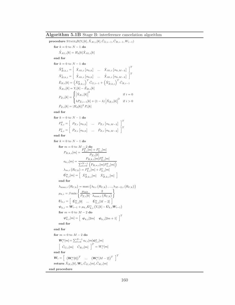
Algorithm 5.1B Stage B: interference cancelation algorithm
procedure Stage B(Yi[k], XA1,i[k], CG,i−1, CR,i−1,Wi−1)
for k = 0 to N − 1 do
ˆXA1,i[k] = Hd[k]XA1,i[k]
end for
for k = 0 to N − 1 do
XgB,k,i
=[
XA1,i
[αk,0
]... XA1,i
[αk,M−2
]]T
XrB,k,i
=[
ˆXA1,i
[αk,0
]...
ˆXA1,i
[αk,M−2
]]T
EB,i[k] =(
XgB,k,i
)TCG,i−1 +
(
XrB,k,i
)TCR,i−1
XB,i[k] = Yi[k]− EB,i[k]
PZ,i[k] =
∣∣∣XB,i[k]
∣∣∣2
if i = 0
λPZ,i−1[k] + (1 − λ)∣∣∣XB,i[k]
∣∣∣2
if i > 0
PZ,i[k] = |Hd[k]|2 Pi[k]
end for
for k = 0 to N − 1 do
Pgk,i
=[
PZ,i
[αk,0
]... PZ,i
[αk,M−2
]]T
P rk,i
=[
PZ,i
[αk,0
]... PZ,i
[αk,M−2
]]T
end for
for k = 0 to N − 1 do
for m = 0 to M − 2 do
PR,k,i[m] =P
gk,i
[m] + P rk,i
[m]
PZ,i[k]
ak,i[m] =PR,k,i[m]P g
k,i[m]
∑N−1n=0
(
PR,n,i[m]P gn,i[m]
)
λm,i
(RU,k
)= P
gk,i
[m] + P rk,i
[m]
Uak,i
[m] =[
XgB,k,i
[m] XrB,k,i[m]
]
end for
λmax,i
(RU,k
)= max
λ0,i
(RU,k
), ..., λM−2,i
(RU,k
)
µk,i = βmin
µinit
PZ,i[k],
2
λmax,i
(RU,k
)
Uk,i =[
Uak,i
[0] ... Uak,i
[M − 2]]
ψk,i =Wi−1 + µk,iU∗
k,i
(Yi[k]−Uk,iWi−1
)
for m = 0 to M − 2 do
ψak,i[m] =
[
ψk,i[2m] ψk,i[2m+ 1]]T
end for
end for
for m = 0 to M − 2 do
W ai [m]=
∑N−1ℓ=0 aℓ,i[m]ψa
ℓ,i[m]
[
CG,i[m] CR,i[m]]T
= W ai [m]
end for
Wi =[
(W a
i [0])T
...(W a
i [M − 2])T
]T
return XB,i[k],Wi, CG,i[m], CR,i[m]
end procedure
160
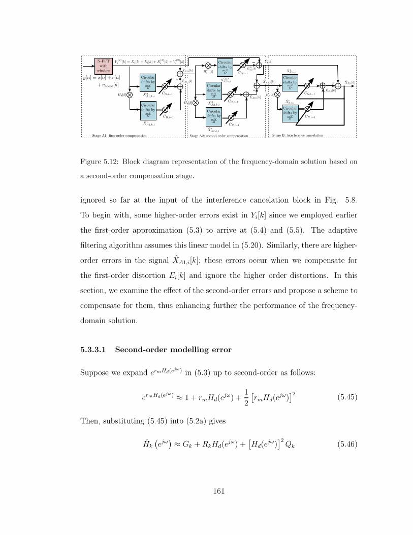
Figure 5.12: Block diagram representation of the frequency-domain solution based on
a second-order compensation stage.
ignored so far at the input of the interference cancelation block in Fig. 5.8.
To begin with, some higher-order errors exist in Yi[k] since we employed earlier
the first-order approximation (5.3) to arrive at (5.4) and (5.5). The adaptive
filtering algorithm assumes this linear model in (5.20). Similarly, there are higher-
order errors in the signal XA1,i[k]; these errors occur when we compensate for
the first-order distortion Ei[k] and ignore the higher order distortions. In this
section, we examine the effect of the second-order errors and propose a scheme to
compensate for them, thus enhancing further the performance of the frequency-
domain solution.
5.3.3.1 Second-order modelling error
Suppose we expand ermHd(ejω) in (5.3) up to second-order as follows:
ermHd(ejω) ≈ 1 + rmHd(e
jω) +1
2
[rmHd(e
jω)]2
(5.45)
Then, substituting (5.45) into (5.2a) gives
Hk
(ejω)≈ Gk +RkHd(e
jω) +[Hd(e
jω)]2Qk (5.46)
161

where Gk and Rk are defined in (5.5) and
Qk =1
M
M−1∑
m=0
gmr2m
2e−j 2π
Mmk (5.47)
Repeating the derivations from (5.18) to (5.20) with the higher order error yields
the following expressions. We can rewrite the output from the FFT block as
Y(2)i [k] = Xi[k] + Ei[k] + E
(2)i [k] + V
(2)i [k]
≈ Xi[k] + Ei[k] + E(2)i [k] (5.48)
where Y(2)i [k] includes the input signal Xi[k] and the first-order distortion Ei[k]
in (5.20). The second-order distortion term is E(2)i [k]. Recall that Vi[k] in (5.20)
represents the spectral leakage and higher order error terms (starting from second-
order and up). Here, V(2)i [k] in (5.48) represents the spectral leakage and higher
order error terms (starting from the third-order and up). In a manner similar to
the vector notation in (5.23) and (5.24), E(2)i [k] can be expressed as:
E(2)i [k] =
(
X(2),rk,i
)T
CQ (5.49a)
CQ =[
Q0 Q1 ... QM−1
]T
(5.49b)
where
X(2),rk,i ,
[
Xi [k] Xi [αk,0] ... Xi [αk,M−2]]T
(5.50a)
Xi[k] , (Hd[k])2Xi [k] (5.50b)
Note that the size of the vectors here is M , while the size of the vectors in
(5.23) and (5.24) is M − 1. Therefore, we see that the input to the interfer-
ence cancelation block includes an additional term E(2)i [k], and we expect the
performance to improve if we remove it. We see from (5.49) that E(2)i [k] is de-
termined by the Qk. From (5.47), we see that Qk is the DFT of the sequence
162

of g0r20, ..., gM−1r2M−1 scaled by 1
2M. Therefore, we can estimate Qk if gmr
2m is
known.
Recall from (5.33d) and (5.32b) that Wk,i[m] are the estimated CG[m] and
CR[m] for m = 0, ...,M − 2 at time i; and from (5.24), CG[m] and CR[m] are
Gm+1 and Rm+1, respectively. From (5.5), we see that Gk and Rk are the DFT of
the sequences of g0, ..., gM−1 and g0r0, ..., gM−1rM−1 scaled by 1M. Using
the estimated Gm+1 and Rm+1 and the assumption that G0 = 1 and R0 ≈ 0, we
can estimate gm and gmrm at time i using the inverse discrete Fourier transform
(IDFT) and scaling it by M :
gm,i =M−1∑
k=0
Gk,iej 2πM
mk (5.51a)
gm,irm,i =
M−1∑
k=0
Rk,iej 2πM
mk (5.51b)
After estimating gm and gmrm, we can estimate gmr2m at time i. Subsequently,
Qk at time i is estimated using (5.47). Therefore, we can obtain a better linear
model for Yi[k] in (5.20) from Y(2)i [k] by removing the second order distortion:
Yi[k] = Y(2)i [k]− E
(2)A2,i[k] (5.52)
where
E(2)A2,i[k] =
(
X(2),rA2,k,i
)T
CQ,i−1 (5.53a)
CQ,i−1 =[
Q0,i−1 Q1,i−1 ... QM−1,i−1
]T
(5.53b)
with Qm,i−1 denoting the estimated Qm in (5.49b) at time i − 1 and X(2),rA2,k,i is
obtained by using the estimated XA1,i[k], from the compensation block in Fig.
5.8, in place of Xi[k] in (5.50b) as:
X(2),rA2,k,i ,
[ˆXi [k]
ˆXi [αk,0] ... ˆXi [αk,M−2]]T
(5.54a)
ˆXi[k] , (Hd[k])2 XA1,i [k] (5.54b)
163

The resulting structure for removing the higher-order terms from Y(2)i [k] is shown
in Fig. 5.12. Comparing with the original solution in Fig. 5.8, a new block is
inserted between the original compensation and interference cancelation blocks.
The top-most path shows how the second-order distortion E(2)A2,i[k] is generated
and removed from Y(2)i [k]. The resultant output Yi[k] is fed into the interference
cancelation block.
5.3.3.2 Second-order compensation error
Recall from (5.26) that we are estimating the first-order distortion as EA1,i[k]
using Yi[k] in place of Xi[k]. After stage A1 of the compensation block in Fig.
5.12, we can find a better estimate for the first-order distortion using XA1,i[k]:
EA2,i[k] =(
XgA2,k,i
)T
CG,i−1 +(
XrA2,k,i
)T
CR,i−1 (5.55)
where EA2,i[k] is the new estimate for E1[k] and XgA2,k,i and X
rA2,k,i are obtained
by replacing Xi[·] in (5.21) and (5.23) by XA1,i[·]:
XgA2,k,i ,
[
XA1,i [αk,0] ... XA1,i [αk,M−2]]T
(5.56a)
XrA2,k,i ,
[ˆXA1,i [αk,0] ... ˆXA1,i [αk,M−2]
]T
(5.56b)
ˆXA1,i [k] = Hd[k]XA1,i [k] (5.56c)
Using EA2,i[k] and E(2)A2,i[k] in (5.55) and (5.53a), respectively, we obtain a better
estimate for Xi[k] as
XA2,i[k] = Y(2)i [k]− EA2,i[k]− E
(2)A2,i[k] (5.57)
The structure for estimating Xi[k] is shown in the middle block of Fig. 5.12. The
resulting output XA2,i[k] is fed into the interference cancelation block. A sum-
mary of the enchanced algorithm and the second-order compensation algorithm
are shown in Algorithm 5.2.
164

Algorithm 5.2 Summary of enhanced frequency-domain solution
Require: Apply N -FFT with windowing (e.g. Blackman-Harris window) on the i−th
block of samples to obtain Y(2)i [k].
Let W−1 = 0, CG,−1 = 0 and CR,−1 = 0.
repeat
% Stage A1: 1st-order compensation
Stage A1(Y(2)i [k], CG,i−1, CR,i−1)
% Stage A2: 2nd-order compensation
Stage A2(Y(2)i [k], XA1,i[k], CG,i−1, CR,i−1)
% Stage B: Interference cancelation
Stage B(Yi[k], XA2,i[k], CG,i−1, CR,i−1,Wi−1)
until end of data blocks
5.4 Comparison with prior work
We will compare the proposed solution against [1,2]; both of these works deal with
similar scenarios. We already explained earlier the differences of our approach
in relation to [1]. With regards to [2], this work relies again on a useful time-
domain solution but it does not exploit the various aspects of the frequency-
domain transformations that the proposed solution considers. For this reason,
the approach of [2] suffers from the same limitation as the time-domain solution:
it is not able to exploit fully information from frequency bands that may be free
of signal components.
There are also some differences with respect to the proposed time-domain
approach as well. The block diagram representation of the solution in [2] is
shown in Fig. 5.13. We will give an overview of the algorithm. In [2], the authors
found that the distortions can be estimated by generating some pseudo-signal
165

Algorithm 5.2A Stage A2: second-order compensation algorithm
Require: Generate CQ,i−1 from CG,i−1, CR,i−1 using (5.51) and (5.47).
procedure Stage A2(Y(2)i [k], XA1,i[k], CG,i−1, CR,i−1)
for k = 0 to N − 1 do
ˆXi[k] = (Hd[k])2 XA1,i [k]
ˆXA1,i [k] = Hd[k]XA1,i [k]
end for
for k = 0 to N − 1 do
X(2),rA2,k,i =
[ˆXi [k]
ˆXi [αk,0] ... ˆXi [αk,M−2]]T
E(2)A2,i[k] =
(
X(2),rA2,k,i
)T
CQ,i−1
Yi[k] = Y(2)i [k]− E
(2)A2,i[k]
XgA2,k,i =
[
XA1,i [αk,0] ... XA1,i [αk,M−2]]T
XrA2,k,i =
[ˆXA1,i [αk,0] ... ˆXA1,i [αk,M−2]
]T
EA2,i[k] =(
XgA2,k,i
)T
CG,i−1 +(
XrA2,k,i
)T
CR,i−1
XA2,i[k] = Yi[k]− EA2,i[k]
end for
return Yi[k], XA2,i[k]
end procedure
166

Figure 5.13: Block diagram representation of algorithm in reference [2].
and multiply it by some parameters wt and wg. In their solution in Fig. 5.13,
the estimated parameters at n − 1 are denoted by wt,n−1 and wg,n−1, and the
estimated distortion is eA[n]. In reference [2], the distortion parameters wg and
wt are related to the gain offsets gm and time offsets rm as follows:
wg ,[
wg1 ... wg(M−1)
]T
(5.58a)
wt ,[
wt1 ... wt(M−1)
]T
(5.58b)
where wtk and wgk are
wg0
...
wg(M−1)
≈ 1
MFH
(1− g0)...
(1− gM−1)
(5.59a)
wt0
...
wt(M−1)
≈ 1
MFH
r0...
rM−1
(5.59b)
167

and FH denote the Hadamard matrix [2]. Suppose M = 4, then FH is
FH =
1 1 1 1
1 −1 1 −1
1 1 −1 −1
1 −1 −1 1
(5.60)
Note that wg0 and wt0 in (5.59) are the average of 1 − gm and rm, respectively.
In [2], both wg0 and wt0 are 0 as the authors assumed that the average of the
gain and time mismatches are 1 and 0, respectively.
The recovered signal xA[n] is obtained by subtracting eA[n] from y[n]. The
pseudo-signal is generated using the Hadamard transform. This is similar to the
first-stage of the proposed time-domain solution and frequency-domain solution
in Figs. 5.7 and 5.8, respectively, where we create the distortions and remove
them from the distorted samples. The difference in our solutions is that our
estimated distortions are not from a pseudo-signal as in [2]; the distortions are
estimated by frequency-shifting the signal instead.
Another difference is in the second stage where the parameters are estimated.
In [2], the authors use the recovered signal xA[n] from the first stage to generate
a new pseudo-signal and correlate it with xA[n]. Their motivation is that if xA[n]
is free from distortions, then the new pseudo-signal should be uncorrelated with
xA[n]. Adjustments are made to the estimated parameters using the correlator
output. For our proposed solutions, our motivation is to use successive cance-
lation where we use the recovered signal in the first stage as an input to the
interference cancelation block to obtain a cleaner signal, xB[n] or XB,i[k]. Ob-
serve also that the recovered signal in the first stage of the proposed time-domain
solution uses the same implementation as [1]. In Section 5.6.2, where we com-
pare the previous works using simulations, we calculate the SNR of the recovered
168
signal in both stages of our proposed solutions. We find that the SNR from the
final stage is better.
5.5 Performance analysis
This section carries out a mean-square analysis of the behavior of the frequency-
domain solution, and derives expressions that characterize its limits of perfor-
mance. The analysis is carried out under some simplifying conditions on the
data that follow from the fact that the DFT helps decorrelate the frequency bins
for sufficiently large N . For this reason, we shall assume whenever necessary that
the signal components across different frequency bins are largely uncorrelated.
We shall also assume that the input signal is wide-sense stationary and has zero-
mean and is uncorrelated of any measurement noise; the latter is assumed to be
white. It can also be shown that when the DFT length is large, the distribu-
tion of the DFT coefficients become Gaussian, and the DFT coefficients become
independent. Under these conditions, we can derive theoretical performance ex-
pressions that will be shown later in the simulations to match well the simulated
performance of the frequency-domain solution. Two useful measures of perfor-
mance are the mean-square-deviation (MSD), and the excess-mean-square error
(EMSE). The EMSE can be used to quantify the improvement in signal-to-noise
ratio (SNR) of the algorithm. These measures are defined in the sequel.
5.5.1 Assumptions on the signal and its distortions
From (5.30) and (5.31), we observe that for the k-th bin, the noise Zk[i] is defined
in terms of the FFT coefficient Xi[k] + Vi[k] of the current bin, while the regressor
Uk,i is made up of FFT coefficients from other bins. It is well-known that the
169

coefficients of the DFT of stationary signals are asymptotically uncorrelated [105].
Therefore, we may assume that when the FFT length N is large, both Xi[k] and
Vi[k] in (5.20) are uncorrelated with Xi[ℓ] and Vi[ℓ], k 6= ℓ, respectively. We also
assume that Xi[k] and Vi[k] are zero mean. Recall further from (5.30) and (5.31)
that the regressor Uk,i contains frequency-shifted components ofXi[k]. Therefore,
we also assume that the Zk[i] and Uk,i are uncorrelated. We also assume that the
Xi[ℓ] and Vi[ℓ] are independent of each other, and Xi[ℓ] and Vi[ℓ] are wide-sense
stationary and zero-mean.
Moreover, in reference [106], it has been shown that for stationary signal,
its DFT coefficients can be assumed to have a Gaussian distribution when the
DFT length is large. Reference [106] also showed that covariance matrix of the
DFT coefficients is nearly diagonal, hence the DFT coefficients are statistically
independent. In our work, we will use this stronger independent assumption (vs
uncorrelated assumption) in some of our analysis (see (5.80), (5.81) and (5.82)).
5.5.2 Statistical properties of data model
Under the assumed statistical conditions, it follows that the variance of Zk[i] in
(5.30) is given by
σ2Z,k , E|Zk[i]|2 = E|Xi[k]|2 + E|Vi[k]|2
= σ2X,k + σ2
V,k
(5.61)
where σ2X,k is the power of the input signal, and σ2
V,k is the power of the unmod-
eled dynamics and spectral leakage in the k-th FFT bin. Moreover, examining
the vector Uk,i in (5.31a), we deduce that its covariance matrix is mainly block
170

diagonal, namely,
RU,k = E[U ∗
k,iUk,i
]
= diag RX,αk,0, ... , RX,αk,M−2
(5.62)
where
RX,ℓ = σ2X,ℓ
1 Hd[ℓ]
(Hd[ℓ])∗ |Hd[ℓ]|2
=
1
(Hd[ℓ])∗
σ2X,ℓ
[
1 Hd[ℓ]]
(5.63)
and RX,αk,mand RU,k are square matrices of size 2 by 2 and 2(M−1) by 2(M−1),
respectively. Note that RX,αk,mand RU,k have ranks one and M −1, respectively.
It also follows from the assumed uncorrelatedness of Xi[k] and Vi[ℓ], for all k 6= ℓ,
that Zk[i] is spatially white:
EZk[i]Z∗ℓ [j] = 0, i, j whenever k 6= ℓ (5.64)
We further assume that Zk[i] is temporally white.
EZk[i]Z∗k [j] = 0, i 6= j (5.65)
The temporal whiteness is satisfied when the FFT length N is large so that the
input signal bandwidth can be assumed to have been divided into small narrow
channels where the signal spectrum is almost flat. Recall from (5.31) and (5.32)
that Zℓ[i] contains Xi[ℓ], and Uk,i contains Xgk,i and X
rk,i, where X
gk,i and X
rk,i are
related to Xi[αk,m] and Xi[αk,m] in (5.23). Therefore, there will be correlation
between Xi[ℓ] and Uk,i if the indices of ℓ and αk,m match. Therefore,
EZℓ[i]U∗k,j[2m] = σ2
X,ℓ δi,j δℓ,αk,m(5.66a)
EZℓ[i]U∗k,j[2m+ 1] = (Hd[ℓ])
∗ σ2X,ℓ δi,j δℓ,αk,m
(5.66b)
171

where m = 0, ...,M − 2 and αk,m is defined in (5.22). When the input to the
FFT is real, Xi[k] has conjugate symmetry. Therefore, we can also write
EZℓ[i]Uk,j[2m] = σ2X,ℓ δi,j δℓ,N−αk,m
(5.67a)
EZℓ[i]Uk,j[2m+ 1] = (Hd[ℓ])∗ σ2
X,ℓ δi,j δℓ,N−αk,m(5.67b)
where the index αk,m in (5.66) is replaced by N − αk,m.
5.5.3 MSD and SNR measures
The error vector Wk,i and the a-priori error ea,k[i] are defined as
Wk,i ,W o −Wk,i (5.68a)
ea,k[i] , Uk,iWk,i−1 (5.68b)
The mean-square-deviation (MSD) and the excess-mean-square-error (EMSE) of
each bin are defined as
MSDk , limi→∞
E‖Wk,i‖2 (5.69a)
EMSEk , limi→∞
E|ea,k[i]|2 (5.69b)
The overall MSD and EMSE measures are defined as the average values across
all bins:
MSD , limi→∞
1
N
N−1∑
k=0
E‖Wk,i‖2 (5.70a)
EMSE , limi→∞
1
N
N−1∑
k=0
E|ea,k[i]|2 (5.70b)
Note that in this work, due to the choice of the combination weights in (5.38),
after combining the intermediate estimates across bins, the error vector Wk,i is
the same for all k. Therefore, the overall MSD is equal to the MSD of each bin:
MSD = limi→∞
E‖Wk,i‖2 (5.71)
172

We can relate the EMSE to the signal-to-noise ratio (SNR) measure as follows.
First, recall the system model for the k-th bin (5.30):
Dk[i] = Xi[k]︸ ︷︷ ︸
desired signal
+Uk,iWo + Vi[k]
︸ ︷︷ ︸
distortion
(5.72)
The expected power of the desired signal and the distortion for each bin are σ2X,k
and (W o)∗RU,kWo+σ2
V,k, respectively. The recovered signal after the interference
cancelation in (5.28) (see Fig. 5.8) can also be rewritten as
XB,i[k] = Yi[k]− EB,i[k]
≈Dk[i]−Uk,iWk,i (5.73a)
= Xi[k]︸ ︷︷ ︸
desired signal
+Uk,iWk,i + Vi[k]︸ ︷︷ ︸
remaining distortion
(5.73b)
The approximation in (5.73a) arises as EB,i[k] from (5.29) is created by estimating
the true regressor Uk,i, whereas in (5.73a), we use true regressor Uk,i instead. The
expected power of Uk,iWk,i as i→ ∞, is the EMSEk in (5.69b). Therefore, across
all bins, the overall SNR of the distorted signal, recovered signal, and the SNR
improvement are
SNRdistorted =
∑N−1k=0 σ
2X,k
∑N−1k=0 (W
o)∗RU,kW o + σ2V,k
(5.74a)
SNRrecovered =
∑N−1k=0 σ
2X,k
N EMSE +∑N−1
k=0 σ2V,k
(5.74b)
SNRimprovement =SNRrecovered
SNRdistorted(5.74c)
5.5.4 Error recursions
To evaluate the performance measures, we first need to examine how the errors
evolve over time. The error recursions corresponding to the adaptive algorithm
173

(5.33) are derived by subtracting W o from them to get
ψk,i =(I2M−2 − µk,iU
∗k,iUk,i
)Wk,i−1
− µk,iU∗k,iZk[i] (5.75a)
ψak,i[m] =
[
ψk,i[2m] ψk,i[2m+ 1]]T
(5.75b)
W ak,i[m] =
N−1∑
ℓ=0
aℓ,i[m]ψaℓ,i[m] (5.75c)
Wk,i =[(
W ak,i[0]
)T
...(
W ak,i[M − 2]
)T ]T
(5.75d)
where m = 0, ...,M − 2. Recall from (5.38) that aℓ,i[m] = aℓ,k,i[m], ∀ k.
Therefore, we use aℓ,i[m] in place of aℓ,k,i[m] in (5.75c). We are interested in
approximating the MSD and EMSE measures in steady-state after the algorithm
has had sufficient time to converge, i.e., as i → ∞. For this reason, we shall
assume that, at that stage, the step-sizes µk,i and the combination coefficients
aℓ,i[m] would have converged towards steady-state values and drop their time
index i. We now collect the recursions from all channels into a single vector
model as follows:
ψi =[
ψT0,i ... ψT
N−1,i
]T
(5.76a)
Wi =[
W T0,i ... W T
N−1,i
]T
(5.76b)
and define the block diagonal matrices M and Ri and vector si:
M , diag µ0I2M−2, ..., µN−1I2M−2 (5.77a)
Ri , diag U ∗0,iU0,i, ..., U ∗
N−1,iUN−1,i (5.77b)
si , col U ∗0,iZ0[i], ..., U ∗
N−1,iZN−1[i] (5.77c)
174

Using (5.62) and (5.66), it can be verified that
ERi , R = diag RU,0, ..., RU,N−1 (5.78a)
Esi = 0 (5.78b)
Let
S , Esis∗i
(5.79)
which is an N by N block matrix with blocks of size 2(M − 1) by 2(M − 1).
Using (5.61) and (5.62), the k-th diagonal block is
Sk,k = σ2Z,kRU,k, k = 0, ..., N − 1 (5.80)
For the p-th block row and k-th block column in S where p 6= k,
Sp,k , EZp[i]U∗p,iUk,iZ
∗k [i] (5.81)
Using (5.31), (5.32) and (5.23), we note that Zp[i] contains Xi[p], while Zk[i]
contains Xi[k] and Up,i contains Xi[αp,m] and Xi[αp,m]. From the assumed spa-
tial independence of Xi[p], we conclude that Zp[i] is independent of Zk[i] and
Up,i. Next, we also see that U ∗k,i contains X∗
i [αk,m] and X∗i [αk,m]. Using the
conjugate symmetry property we have, X∗i [αk,m] = Xi[N −αk,m] and X
∗i [αk,m] =
Xi[N − αk,m]. Therefore, Zp[i] is correlated with U ∗k,i when the indices p and
N −αk,m match. Applying the same reasoning to Zk[i] on U∗p,i, we see that Zk[i]
is correlated with U ∗p,i when the indices k and N − αp,m match. Therefore, it
follows that
Sp,k = E (Zk[i]Up,i)∗ (Zp[i]Uk,i) , p 6= k
=([
1 Hd[k]]
Pk,p
)∗ ([1 Hd[p]
]
Pp,k
)
= P Tk,p
1
(Hd[k])∗
[
1 Hd[p]]
Pp,k (5.82)
175

where p and k are in 0, ..., N − 1 and matrix Pp,k is
Pp,k = σ2X,p
[
I2 δp,N−αk,0... I2 δp,N−αk,M−2
]
(5.83)
We can rewrite (5.75d) as
Wk,i =
N−1∑
ℓ=0
Aℓψℓ,i (5.84a)
Aℓ = diag aℓ[m]I2, ..., aℓ[M − 2]I2 (5.84b)
N−1∑
ℓ=0
Aℓ = I2M−2 (5.84c)
A block matrix representation of (5.84) is shown in (5.85).
W0,i
.
..
WN−1,i
=
W a0,i[0]
.
..
W a0,i[M − 2]
W0,i
.
..
WN−1,i
=
a0[0]I2
. . .
a0[M − 2]I2
︸ ︷︷ ︸
A0:(2M−2)×(2M−2) diagonal matrix
...
aN−1[0]I2
. . .
aN−1[M − 2]I2
︸ ︷︷ ︸
AN−1
... ......
A0 ... AN−1
ψa0,i[0]
..
.
ψa0,i[M − 2]
..
.
ψaN−1,i[0]
...
ψaN−1,i[M − 2]
=
I2M−2
...
I2M−2
[
A0 ... AN−1
]
ψ0,i
...
ψN−1,i
(5.85)
176

From (5.85), we define the matrix A for all bins as
AT , KAT (5.86a)
K ,[
I2M−2 ... I2M−2
]T
(5.86b)
A ,[
A0 ... AN−1
]T
(5.86c)
Therefore, substituting (5.75a) into (5.85), we conclude that, in steady-state,
the error vectors across all channels evolve over time according to the following
recursion:
Wi = AT(IN(2M−2) −MRi
)Wi−1 −ATMsi, i ≥ 1 (5.87)
5.5.5 Combination weights and stepsizes
From (5.30), the interference term is Uk,iWo. We assume that when the solution
converges, the residual error Uk,iWk,i is smaller than the signal component and
unmodelled dynamics (together asZk[i]). Therefore, when the solution converges,
the average power in each recovered bin can be approximated by σ2Z,k. The
combination weights aℓ[m] in (5.84) are based on (5.38), where we have dropped
the indices k from aℓ,k[m]. Let us examine aℓ[m] for m = 0. In (5.37), we see that
the numerator is P gℓ [m] + P r
ℓ [m]. From (5.36), we see that P gℓ [0] ≈ PZ [αℓ,0] and
P rℓ [0] ≈ PZ [αℓ,0]. From (5.35), PZ [αℓ,0] and PZ [αℓ,0] are the estimated power of the
recovered signal and its “derivative” in the αℓ,0-th channel, which are σ2Z,αℓ,0
and
σ2Z,αℓ,0
|Hd[αℓ,0]|2, respectively. Similarly, in (5.37), we see that the denominator
is PZ [ℓ] = σ2Z,ℓ. Therefore, the converged combination weights in (5.84b) can be
approximated as:
aℓ[m] ≈ γmγℓ,m (5.88)
177

where
γm =
(N−1∑
k=0
γk,m
)−1
(5.89a)
γℓ,m =σ4Z,αℓ,m
σ2Z,ℓ
(1 + |Hd[αℓ,m]|2
)(5.89b)
We assume that σ2Z,ℓ > 0 for all ℓ and hence, γℓ,m > 0. Therefore, the combination
weight aℓ[m] is always positive.
0 < aℓ[m] < 1 (5.90)
Recall from (5.43) and (5.44) that the stepsizes µℓ are bounded by the eigenvalues
of RU,ℓ. From (5.41) and (5.36), we see that the eigenvalues are estimated as the
sum of PZ [αℓ,m] and PZ [αℓ,m]. These quantities can be expressed as σ2Z,αℓ,m
and
σ2Z,αℓ,m
|Hd[αℓ,m]|2, respectively. Therefore, the step-sizes satisfy the bound:
µℓ ≤2
σ2Z,αℓ,m
(1 + |Hd[αℓ,m]|2), m = 0, ...,M − 2 (5.91)
From (5.62) and (5.63), we see that the non-zero eigenvalues of RU,ℓ are the
non-zero eigenvalues of the rank-1 matrix RX,αℓ,m. The non-zero eigenvalue of
RX,αℓ,mis the trace σ2
X,αℓ,m(1 + |Hd[αℓ,m]|2). Since σ2
X,ℓ < σ2Z,ℓ, the eigenvalues of
µℓRX,αℓ,mis bounded by
λmax
(µℓRX,αℓ,m
)≤
2σ2X,αℓ,m
σ2Z,αℓ,m
< 2 (5.92)
5.5.6 Convergence in mean
Taking expectation of both sides of (5.87) and using (5.78) and (5.86), we obtain
EWi = (KB)EWi−1 (5.93)
where
B , AT(IN(2M−2) −MR
)(5.94)
178

Asymptotic mean stability is guaranteed when
ρ (KB) < 1 (5.95)
where ρ(·) denotes the spectral radius of its matrix argument. In appendix 5.A,
we show that conditions (5.90) and (5.92) ensure (5.95) so that stability in the
mean is guaranteed.
5.5.7 Mean square stability
In this section, we derive the MSD and EMSE measures defined in (5.69) and
(5.70). From [109], it is known that
E|ea,k[i]|2 = E‖Wk,i‖2RU,k(5.96)
where the notation ‖x‖2A denotes the squared weighted Euclidean norm x∗Ax.
We therefore proceed to evaluating the expression for E‖Wk,i‖2Σkfor an arbitrary
Hermitian non-negative definite matrix Σk. Setting Σk = RU,k or I2M−2 yields the
MSD or EMSE expressions in (5.69) and (5.70), respectively. First using (5.86),
we re-write (5.87) more compactly as
Wi = BiWi−1 − Gsi, i ≥ 0 (5.97a)
Bi , AT(IN(2M−2) −MRi
)(5.97b)
G , ATM = KATM (5.97c)
From (5.93) and (5.94), we can also denote the mean of Bi as
B , EBi = KB (5.98)
Finally, using (5.79), we introduce the matrices F and Y as
F , BT ⊗ B∗
Y , GSGT(5.99)
179

where ⊗ denotes the Kronecker product. In [109], for small step sizes, it was
argued that if F is stable, then (5.97) is mean-square stable. Moreover, if B is
stable, then F is stable.
5.5.8 MSD and EMSE
Following the same arguments from [109], the MSD and EMSE in (5.70) are given
by the following expressions:
MSD =1
N
[vec(YT )]T (I − F)−1 vec
(IN(2M−2)
)(5.100a)
EMSE =1
N
[vec(YT )]T (I − F)−1 vec (R) (5.100b)
where the vec operator vectorizes its matrix argument by stacking the columns
on top of each other, and R is defined in (5.78).
Due to the structure of A, where all estimates after the combination step are
the same, we can use (5.86) to reduce (5.97) to a single node recursion. Thus
note first that
KWk,i = KAT(IN(2M−2) −MRi
)
︸ ︷︷ ︸Bi
KWk,i︸ ︷︷ ︸
Wi−1
−KATM︸ ︷︷ ︸
G
si (5.101)
Multiplying both sides of (5.101) by 1NKT and noting that 1
NKKT = I2M−2, we
obtain the single node recursion as:
Wk,i = Bnode,iWk,i−1 − Gnodesi, i ≥ 0 (5.102a)
Bnode,i , AT(IN(2M−2) −MRi
)K (5.102b)
Gnode , ATM (5.102c)
180

Hence, the MSD, EMSEk and EMSE can also be written as
MSD = hTnode vec (I2M−2) (5.103a)
EMSEk = hTnode vec (RU,k) (5.103b)
EMSE =1
N
N−1∑
k=0
hTnode vec (RU,k)
=1
NhTnode vec
(KTRK
)(5.103c)
where
hTnode ,[vec(YT
node
)]T(I −Fnode)
−1 (5.104a)
Bnode , EBnode,i = BK (5.104b)
Fnode , BTnode ⊗ B∗
node (5.104c)
Ynode , GnodeSGTnode (5.104d)
The advantage of using (5.103) over (5.100) is that the matrices YTnode and Fnode
are much smaller compared to YT and F .
5.6 Simulations results
The simulations in this section are carried out by generating a random Gaussian
signal with variance equal to one. The signal is either low-pass or band-pass
filtered according to the desired simulation settings. This signal is the clean in-
put signal to the ADC. Sinc interpolation is used to create the distorted signal
with some time and gain offsets. The gain and time offsets are randomly gen-
erated; their standard deviation is set to 0.01 and their means are set to 1 and
0, respectively. The time offsets and gain mismatches when M = 4 are -7.55,7.60, 9.60, -9.65 × 10⁻³ and 0.9994, 0.9998, 1.0126, 0.9881, respectively. The
step-sizes used in the time-domain solution (5.15) and frequency-domain solution
181

(5.44) are set to µ = 1.75 × 10⁻⁶ and µinit = 2 × 10⁻⁴, respectively. The factor
β in (5.44) is set to 1. The FFT length is 210. The FFT windowing function is
the Blackman-Harris window. The number of ADCs M = 4. The λ used in the
averaging of (5.39) is 0.95.
5.6.1 MSD and SNR measures
Recall from (5.30) and (5.33d) that the true and estimated distortion parameter
at the i-th block are W o and Wi, respectively. The estimation error is defined as
Wi =W o −Wi. The mean-square-deviation (MSD) is defined as
MSD = limi→∞
E‖Wi‖2 (5.105)
In the simulations, the MSD is calculated by averaging ‖Wi‖2 over some runs. The
signal power to noise power ratio (SNR) of the distorted signal and the recovered
signal can also be calculated from the simulations. From (5.30) and (5.28), at
the i-th block, we denote the power of the input signal, original distortion and
the residual error after the interference cancelation block as:
Psignal =
N−1∑
k=0
|Xi[k]|2 (5.106a)
Pdistortion =N−1∑
k=0
|Yi[k]−Xi[k]|2 (5.106b)
Presidual =N−1∑
k=0
|XB,i[k]−Xi[k]|2 (5.106c)
Psignal, Pdistortion and Presidual can be averaged over some runs, and the average
SNR of the original distorted signal and the recovered signal is calculated as:
SNRdistorted =“average” of Psignal
“average” of Pdistortion(5.107a)
SNRrecovered =“average” of Psignal
“average” of Presidual(5.107b)
182

5.6.2 Comparing with prior works
Our first set of simulations compare our proposed algorithms with some prior
works [1, 2]. The comparison shows that the frequency-domain approach gives
better performance. Recall in Section 5.4 that we discussed that our solutions
compensate the distorted signal in the first stage, and then use it in the interfer-
ence cancelation block (stage B of Fig. 5.8 and 5.12) to recover a better signal.
As such, in the simulations, we calculate the SNR of the recovered signal from
both stages.
Recall that the distortion parameters in the various solutions are different.
For the frequency-domain solution, the distortion parameters are Gk and Rk in
(5.5). For our proposed time-domain solution and the work in [1], the distortion
parameters are the same cg and cr in (5.10). For [2], the distortion parameters are
wg and wt, defined in (5.58) and (5.59). Therefore, to compare the estimation
errors from the various solutions using the MSD measure defined in (5.105),
we have to convert all the estimates to the distortion parameters used for the
frequency-domain solution. We can convert cg and cr to Gk and Rk:
Gk =
cg[2k − 2] + jcg[2k − 1] if 1 ≤ k ≤ M2− 1
cg[2k − 2] if k = M2
G∗N−k otherwise
(5.108)
and
Rk =
cr[2k − 2] + jcr[2k − 1] if 1 ≤ k ≤ M2− 1
cr[2k − 2] if k = M2
R∗N−k otherwise
(5.109)
183

For the distortion parameters wg and wt in [2], we first convert them to gm and
rm using (5.58) and (5.59):
g0...
gM−1
=
1...
1
−MF−1
H
wg0
...
wg(M−1)
(5.110a)
r0...
rM−1
=MF−1
H
wt0
...
wt(M−1)
(5.110b)
Once gm and rm are obtained, we can use (5.5) to find Gk and Rk. Therefore, in
the simulations, we can calculate and plot the MSD of the various solutions as
defined in (5.105) and (5.71) and compare their performance.
Similarly, we also compare the SNR measure defined in (5.107) and (5.74) for
the various solutions. For the comparison, we applied the same windowed-FFT
used in the proposed frequency-domain solution on the recovered signals from
the time-domain solutions, and calculate the SNR for each FFT block. The SNR
of the last block is tabulated for comparison purposes.
5.6.2.1 Low-pass input signal
Recall that reference [1] assumes that there exists an out-of-band region, and
uses a high-pass filter to estimate the distortion parameters in that region (recall
Figs. 5.4 and 5.3). Therefore, in this simulation, we simulate a low-pass signal
with a bandwidth of 0.7π, the high-pass filter’s cutoff point is set to 0.8π. We
denote the algorithm in reference [1] as “Vogel’s solution”. We also implemented
the algorithm in reference [2] and denote it as “Matsuno’s solution”. The length
of the input data is 221, the FFT length is 210 and the simulation results are
averaged over 30 experiments.
184

Table 5.1: SNR of the distorted and recovered low-pass signal.
Description SNR [dB]
Distorted signal 37.02
Matsuno’s solution [2] 51.28
Time-domain solution (Stage A of Fig. 5.7) 52.27
Time-domain solution (Stage B of Fig. 5.7) 52.32
Vogel’s solution [1] 68.11
Frequency-domain solution (a) (Stage A1 of Fig. 5.8) 69.98
Frequency-domain solution (a) (Stage B of Fig. 5.8) 77.88
Frequency-domain solution (b) (Stage A2 of Fig. 5.12) 78.30
Frequency-domain solution (b) (Stage B of Fig. 5.12) 81.15
Fig. 5.14 shows the simulation results averaged over 30 runs. The aver-
age SNR of the distorted signal and the average SNR of the recovered signal
after using the various algorithms are shown in Table 5.1. The SNR of the dis-
torted signal is 37dB. In this scenario, when all the distortion components are
present in the out-of-band region, Vogel’s solution works very well and the SNR
of the recovered signal is high (68dB). Both our time-domain and Matsuno’s
solution are able to improve the SNR (∼52dB), albeit at a worse performance
level. This is because the algorithms use the entire bandwidth of the data to
estimate the distortion parameters. In this case, the input signal becomes the
“noise”. For Vogel’s solution, the out-of-band region contains only the distortion
signal. Hence, the time-domain and Matsuno’s solutions require more samples.
The frequency-domain solutions (a) and (b) use the structures of Figs. 5.8 and
5.12, respectively. We recall that the proposed frequency-domain solutions exam-
ine the frequency content of the signal and selectively emphasize the estimation
185

Figure 5.14: Comparing various algorithms on a low-pass signal at 0.7π. The frequency-
domain solutions (a) and (b) use the proposed structures in Figs. 5.8 and 5.12, respec-
tively.
in regions where there is less “noise” via the combination weights (5.38) and the
stepsizes (5.44). Therefore, the frequency-domain solutions converge faster than
the proposed time-domain solution. Moreover, we see that the frequency-domain
solutions obtain a significant improvement in MSD over all other solutions. The
MSD plot also shows that the frequency-domain solution (b), where the second
order distortion is removed, gives a further 10dB improvement over the frequency-
domain solution (a). The SNR of the recovered signal using the frequency-domain
solutions are also better than the time-domain solutions, i.e., 78dB to 81dB.
When we compare the SNR of the recovered signals in both stages of our
algorithms, we note that stage B of the proposed solutions gives a better SNR.
The averaged spectrum of the distorted signal and the recovered signal using the
186

frequency-domain solution is shown in the left plot of Fig. 5.15. Note that the
SNR improvement of the recovered signal is over the entire bandwidth of the
signal. The spectrum plots show the reduction of the distortion spectrum in the
out-of-band region. We noted that, visually, the spectrum of the recovered signal
using the frequency-domain solutions (a) and (b) are similar.
100 200 300 400 500−120
−100
−80
−60
−40
−20
0
FFT bin
Av
era
ge
d p
ow
er
sp
ec
tru
m [
dB
]
Distorted signal
Recovered signal
100 200 300 400 500−120
−100
−80
−60
−40
−20
0
FFT bin
Av
era
ge
d p
ow
er
sp
ec
tru
m [
dB
]
Distorted signal
Recovered signal
Distorted signal
Frequency−domain solution
Distorted signal
Frequency−domain solution
Figure 5.15: The left and right plots show the spectrum of the distorted and recovered
signals using the frequency-domain solution for the two scenarios of a low-pass signal
(left) and a bandpass signal (right).
5.6.2.2 Band-pass input signal
Now, we change the input signal to a band-pass signal from 0.2π to 0.8π. As
discussed in Section 5.2.3, Vogel’s solution will not work in this scenario as one
of the distortion components is within the input signal’s bandwidth (recall Fig.
5.5c). If the high-pass filter’s cutoff point is set to 0.8π as in the previous simula-
tion, it will fail dramatically since some of the original signal’s bandwidth (from
187

0.7π to 0.8π) leaks into the high-pass region, and the SNR of the recovered signal
will be worse than the distorted signal itself. As such, we change the high-pass
filter’s cutoff point to 0.85π. This reduces the leakage and allows the algorithm to
estimate the distortions that are outside the signal’s bandwidth. We will denote
the results when the high-pass cutoff is at 0.8π and 0.85π as Vogel’s solution (a)
and (b), respectively. For the other algorithms, their parameters remain as in
the previous set of simulations. However, as one distortion component is com-
pletely within the signal bandwidth, the algorithms take more time to converge.
Therefore, we increase the input data samples to 221 × 5.
Table 5.2: SNR of the distorted and recovered band-pass signal.
Description SNR [dB]
Distorted signal 35.47
Matsuno’s solution [2] 50.23
Time-domain solution (Stage A of Fig. 5.7) 51.13
Time-domain solution (Stage B of Fig. 5.7) 51.21
Vogel’s solution (a) [1] 27.73
Vogel’s solution (b) [1] 44.08
Frequency-domain solution (a) (Stage A1 of Fig. 5.8) 56.93
Frequency-domain solution (a) (Stage B of Fig. 5.8) 57.26
Frequency-domain solution (b) (Stage A2 of Fig. 5.12) 57.27
Frequency-domain solution (b) (Stage B of Fig. 5.12) 57.28
Fig. 5.16 shows the MSD for the various algorithms and Table 5.2 shows
the SNR of the distorted and recovered signals. The figure and table show that
the frequency-domain solutions perform better than the other algorithms. More
importantly, recall that the algorithms’ parameters used in the low-pass input
188

Figure 5.16: Comparing various algorithms on a band-pass signal from 0.2π to 0.8π.
The simulation results for Vogel’s solution (a) and (b) use a high-pass filter cutoff at
0.8π and 0.85π, respectively.
signal case remains the same in the band-pass signal case; However, for the
frequency-domain solution, the stepsizes and combination weights are adaptive
to the input signal, and is able to adapt these algorithm parameters accordingly.
As a result, the convergence rate is adaptively reduced to obtain MSD and SNR
of -60dB and 57dB, respectively. We also noted that in the band-pass signal case,
removing the second-order distortion does not improve performance. As Vogel’s
solution cannot estimate all the distortion components, it gives the worst SNR
and MSD performance. Vogel’s solution (a) performs worse than Vogel’s solution
(b) because the actual signal leaks into the out-of-band region; This breaks the
assumption that the out-of-band region contains only distortions.
For our proposed time-domain solution and Matsuno’s solution, the stepsize
189

used in their algorithm is the same as the previous simulation. Hence, unlike
the frequency-domain solutions, they are not able to adapt to the input signal.
Although they converge faster, their MSD and SNR performance is worse. If a
designer were to use either of these two solutions, and would like to get similar
MSD and SNR performance as the frequency-domain solution, then the designer
needs to reduce the stepsize. However, this will further reduce their slow con-
vergence rate for the low-pass input signal scenario in the previous section (see
Fig. 5.14). For the sake of completeness, we emprically reduce the stepsizes of
the proposed time-domain solution and Matsuno’s solution by a factor of 0.2 to
obtain MSD and SNR that are similar to the frequency-domain solution. The
SNR is in Table 5.3 and the MSD curve is in Fig. 5.17.
Table 5.3: SNR of the distorted and recovered band-pass signal after reducing the
stepsizes for the time-domain solution and Matsuno’s solution.
Description SNR [dB]
Distorted signal 35.47
Matsuno’s solution [2] 56.62
Time-domain solution (Stage A of Fig. 5.7) 57.73
Time-domain solution (Stage B of Fig. 5.7) 58.03
Frequency-domain solution (a) (Stage A1 of Fig. 5.8) 56.93
Frequency-domain solution (a) (Stage B of Fig. 5.8) 57.26
The frequency-domain solution tries to exploit the case when the distortion
components leaks into empty frequency bands, and the algorithm detects them
and weighs the estimated distortion parameters more in these frequency bands.
For the band-pass case where it is centered at π2, as shown in Fig. 5.5c, we see
that there is at least one distortion component (one of the smaller triangles) lies
190
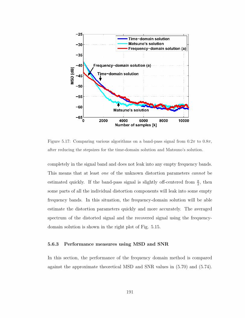
Figure 5.17: Comparing various algorithms on a band-pass signal from 0.2π to 0.8π,
after reducing the stepsizes for the time-domain solution and Matsuno’s solution.
completely in the signal band and does not leak into any empty frequency bands.
This means that at least one of the unknown distortion parameters cannot be
estimated quickly. If the band-pass signal is slightly off-centered from π2, then
some parts of all the individual distortion components will leak into some empty
frequency bands. In this situation, the frequency-domain solution will be able
estimate the distortion parameters quickly and more accurately. The averaged
spectrum of the distorted signal and the recovered signal using the frequency-
domain solution is shown in the right plot of Fig. 5.15.
5.6.3 Performance measures using MSD and SNR
In this section, the performance of the frequency domain method is compared
against the approximate theoretical MSD and SNR values in (5.70) and (5.74).
191

The algorithm’s settings are the same as before and the FFT length is varied from
29, 210 and 211. The input signal used is either a low-pass signal or a band-pass
signal with some varying bandwidth. Recall that our frequency-domain solution
in Fig. 5.8 can also be extended to remove higher order distortion in Fig. 5.12.
As in the previous sections, we will label the solutions as solution (a) and (b),
respectively. We will show that in some cases, solution (b) improves the MSD
and approaches the theoretical performance.
5.6.3.1 Low-pass input signal
When the input signal is a low-pass signal, the bandwidth is varied from 0.1π,
0.3π, 0.5π, 0.7π to 0.9π radians/sample. The input signal data length for the
first four bandwidth regions and for the last bandwidth region are (218) × 5
and (221) × 5, respectively. The results are averaged over 30 runs. Using the
frequency-domain solution (a), the MSD (left-sided plot) and SNR (right-sided
plot) results are shown in Fig. 5.18. From the MSD plot, we noted that increas-
0.2 0.4 0.6 0.8−115
−110
−105
−100
−95
−90
−85
−80
−75
−70
MS
D [
dB
]
Normalized bandwidth of low−pass signal
Proposed solution with 512 FFT
Proposed solution with 1024 FFT
Proposed solution with 2048 FFT
Theory
0.2 0.4 0.6 0.830
40
50
60
70
80
90
100
110
120
SN
R [
dB
]
Normalized bandwidth of low−pass signal
Distorted signal
Proposed solution with 512 FFT
Proposed solution with 1024 FFT
Proposed solution with 2048 FFT
Theory
Figure 5.18: Performance of solution (a), which removes the first order distortions, as
lowpass signal’s bandwidth varies from 0.1π to 0.9π.
192

ing the FFT length did not improve the MSD performance significantly, and the
curves do not match the theoretical performance. We found that the mismatch
is due to the higher order distortions that we have ignored; When we remove
the second-order distortion in solution (b), we found that the simulation results
match with the theory (see Fig. 5.19). However, the SNR plots show that the
SNR performance in both solution (a) and (b) match well with the theoretical
performance. Depending on the input signal’s bandwidth, the distorted signal’s
and recovered signal’s SNR ranged between 35dB to 41dB and 70dB to 90dB,
respectively. From the SNR plot, we see that increasing the FFT length improves
the SNR; especially when the input signal bandwidth is smaller, but not as signif-
icant at larger bandwidth. From the SNR plot, using 1024 FFT, we see that the
SNR of the recovered signal (black line with square marker) varies from 86dB to
79dB as the bandwidth increases, and the SNR improvement from the distorted
signal (green line with diamond) is about 45dB.
Using the frequency-domain solution (b), the MSD (left-sided plot) and SNR
(right-sided plot) results are shown in Fig. 5.19. Now, from the MSD plot,
we noted that the simulation results approach the theoretical performance. We
also noted that doubling the FFT length improves the MSD result by 8dB to
10dB. The SNR plot shows that the simulation performance match well with the
theoretical performance (similar to solution (a)).
5.6.3.2 Band-pass input signal
When the input signal is a band-pass signal (centered at 0.5π), the bandwidth
is varied from 0.2π, 0.4π, 0.6π, 0.8π to 0.94π radians/sample. The input signal
data length is (221) × 10. The results are averaged over 30 runs. The perfor-
mance results using both solutions (a) and (b) are shown in Figs. 5.20 and 5.21,
193

0.2 0.4 0.6 0.8−115
−110
−105
−100
−95
−90
−85
−80
−75
−70
MS
D [
dB
]
Normalized bandwidth of low−pass signal
Proposed solution with 512 FFT
Proposed solution with 1024 FFT
Proposed solution with 2048 FFT
Theory
0.2 0.4 0.6 0.830
40
50
60
70
80
90
100
110
120
SN
R [
dB
]
Normalized bandwidth of low−pass signal
Distorted signal
Proposed solution with 512 FFT
Proposed solution with 1024 FFT
Proposed solution with 2048 FFT
Theory
Figure 5.19: Performance of solution (b), which removes the first and second order
distortions, as lowpass signal’s bandwidth varies from 0.1π to 0.9π.
respectively. First, we noted that for the band-pass signal, both solutions give
the same performance. The results also show that increasing the FFT length im-
proves the performance. Using 1024 FFT, the SNR of the recovered signal (black
line with square marker) varies from 53dB to 57dB, and the SNR improvement
from the distorted signal (green line with diamond) is about 19dB to 22dB.
5.7 Discussion and conclusion
We proposed time-domain and frequency-domain solutions to mitigate the timing
and gain mismatches in TI-ADC. One of the main advantages of this work over
prior works is that it does not need to assume an out-of-band frequency region. By
spliting the input signal into separate FFT bins and modelling each frequency bin
as a node in a network, we are able to exploit adaptive diffusion strategies [109]
to get better performance over the time-domain approach. Consequently, we
showed that the frequency-domain solution is able to adapt to different scenarios;
194

0.2 0.4 0.6 0.8−66
−64
−62
−60
−58
−56
−54
−52
−50
−48
MS
D [
dB
]
Normalized bandwidth of band−pass signal
Proposed solution with 512 FFT
Proposed solution with 1024 FFT
Proposed solution with 2048 FFT
Theory
0.2 0.4 0.6 0.830
35
40
45
50
55
60
65
70
75
80
SN
R [
dB
]
Normalized bandwidth of band−pass signal
Distorted signal
Proposed solution with 512 FFT
Proposed solution with 1024 FFT
Proposed solution with 2048 FFT
Theory
Figure 5.20: Performance of solution (a), which removes the first and second order
distortions,as bandpass signal’s bandwidth varies from 0.2π to 0.94π.
it performs as well as the prior works (which assume out-of-band region), and
also in cases when the prior works fail. Using simulations, we verified that the
derived performance measures match well with the experimental results.
5.A Proof for mean convergence
This appendix proves that conditions (5.90) and (5.92) ensure (5.95) and, hence,
ensure mean stability in the long term regime as i → ∞. To begin with, it
is known that for any two matrices, the products XY and Y X have the same
eigenvalues, counting multiplicity and eigenvalues equal to 0 [113]. Therefore,
ρ(KB) = ρ(BK). Recall that matrix B is defined in (5.94). Using M from
(5.77a), R from (5.78a), Aℓ from (5.84b), AT in (5.86c), and RU,k from (5.62),
195

0.2 0.4 0.6 0.8−66
−64
−62
−60
−58
−56
−54
−52
−50
−48
MS
D [
dB
]
Normalized bandwidth of band−pass signal
Proposed solution with 512 FFT
Proposed solution with 1024 FFT
Proposed solution with 2048 FFT
Theory
0.2 0.4 0.6 0.830
35
40
45
50
55
60
65
70
75
80
SN
R [
dB
]
Normalized bandwidth of band−pass signal
Distorted signal
Proposed solution with 512 FFT
Proposed solution with 1024 FFT
Proposed solution with 2048 FFT
Theory
Figure 5.21: Performance of solution (b), which removes the first and second order
distortions, as bandpass signal’s bandwidth varies from 0.2π to 0.94π.
the block representation for B is shown in (5.111).
B , AT(IN(2M−2) −MR
)
= AT −[
µ0A0RU,0 ... µN−1AN−1RU,N−1
]
(5.111)
Multiplying (5.111) by K from (5.86b), and using the property in (5.84c), we
obtain the expression
BK =N−1∑
k=0
Ak −N−1∑
k=0
µkAkRU,k
= I2M−2 −N−1∑
k=0
µkAkRU,k
= diag
I2 −N−1∑
k=0
µkak[0]RX,αk,0, ...,
I2 −N−1∑
k=0
µkak[M − 2]RX,αk,M−2
(5.112)
196

Using (5.112), mean stability holds when
1 > ρ (BK)
= maxm=0,...,M−2
ρ
(
I2 −N−1∑
k=0
µkak[m]RX,αk,m
)
(5.113)
We note that the matrix sum∑N−1
k=0 µℓak[m]RX,αk,min (5.113) is Hermitian as
RX,αk,mis Hermitian and the coefficients are real. This means that the matrix sum
has real eigenvalues. Now, we need to verify that (5.113) holds using conditions
(5.90) and (5.92). We establish (5.113) in two steps. The first step is to prove
that the matrix sum has positive eigenvalues,
λmin
(N−1∑
k=0
µkak[m]RX,αk,m
)
> 0 (5.114)
where λmin(· ) represents the minimum eigenvalue of the matrix argument. The
second step is to prove that the maximum eigenvalue of the matrix sum is bounded
by 2:
λmax
(N−1∑
k=0
µkak[m]RX,αk,m
)
< 2 (5.115)
The two steps (5.114) and (5.115) imply that the matrix sum contains eigenvalues
between 0 and 2 so that
ρ
(
I2 −N−1∑
k=0
µkak[m]RX,αk,m
)
< 1 (5.116)
Let us proceed with the first step. Using RX,ℓ from (5.63), and the conjugate
symmetry property of Hd[k],we find that
RX,N−ℓ = σ2X,N−ℓ
1 Hd[N − ℓ]
(Hd[N − ℓ])∗ |Hd[N − ℓ]|2
= σ2X,ℓ
1 (Hd[ℓ])
∗
Hd[ℓ] |Hd[ℓ]|2
= conj (RX,ℓ)
(5.117)
197

where the operator conj applies the conjugation operation elementwise. Note
that RX,N−ℓ and RX,ℓ are both rank-1 matrices. Also, note that when ℓ is 0 or N2,
RX,ℓ is real. We will show in the next paragraph that combining the conjugate
pairs will make the sum of matrices in (5.114) contain only positive eigenvalues.
We assume that there exists some αk,m-th FFT channel and its conjugate
channel that contain some signal content (i.e., σ2X,αk,m
> 0). Let us verify that
λmin
(
µkak[m]RX,αk,m+ µk′ak′[m]RX,αk′,m
)
> 0 (5.118)
where k′ represents the appropriate index that matches the conjugate counterpart
of RX,αk,m. Using the rank-1 decomposition of the two matrices from (5.63):
µkak[m]RX,αk,m= µkak[m]σ2
X,αk,mbαk,m
b∗αk,m
µk′ak′[m]RX,αk′,m= µk′ak′[m]σ2
X,αk′ ,mbαk′ ,m
b∗αk′,m
bαk,m=[
1 (Hd[αk,m])∗]T
(5.119)
Now, we denote
ck,m , µkak[m] (5.120)
Using (5.90), we see that ck,m > 0. We can write the sum in (5.118) as:
ck,mRX,αk,m+ ck′,mRX,αk′,m
= σ2X,αk,m
[
bαk,mbαk′,m
]
ck,m 0
0 ck′,m
b∗αk,m
b∗αk′ ,m
= Γαk,mΓ∗αk,m
(5.121)
where
Γαk,m= σX,αk,m
[
bαk,mbαk′,m
]
√ck,m 0
0√ck′,m
(5.122)
It can be verified that bαk,mand bαk′,m
are linearly independent and, hence, and
Γαk,mis non-singular and (5.121) is positive-definite. Hence, (5.118) is true. This
198

means that at least one pair sum from (5.114) is positive-definite and, therefore,
the sum in (5.114) is positive-definite so that (5.114) holds.
Next, we cover the second step (5.115) of the argument. Using (5.92), we can
bound (5.115) by:
λmax
(N−1∑
k=0
µkak[m]RX,αk,m
)
≤N−1∑
k=0
ak[m]λmax
(µkRX,αk,m
)
< 2N−1∑
k=0
ak[m]
< 2 (5.123)
5.B Proof for (5.1)
Consider an ideal M-channel TI-ADC with a sampling interval of Ts and a input
signal of x(t). Assume it is band-limited to the Nyquist frequency, i.e. X(jΩ) = 0
for |Ω| ≥ Ωs
2, Ωs =
2πTs. The sampled signal xs(t) is
xs(t) =
M−1∑
m=0
∞∑
ℓ=−∞δ(t− ℓMTs −mTs)x(t) (5.124)
Now, consider the M-channel TI-ADC has gain and timing mismatches of gm
and rmTs, respectively. The sampled signal ys(t) becomes
ys(t) =M−1∑
m=0
∞∑
ℓ=−∞gmδ(t− ℓMTs −mTs − rmTs)x(t)
=
M−1∑
m=0
∞∑
ℓ=−∞gmδ(t− ℓMTs −mTs)x(t+ rmTs)
=M−1∑
m=0
[ ∞∑
ℓ=−∞δ(t− ℓMTs −mTs)
]
gmx(t+ rmTs)
(5.125)
199

First, we state the below well-known Fourier transform (FT) properties (impulse
train, time-delay and multiplication in time):
F ∞∑
n=−∞δ (t− nTs)
= Ωs
∞∑
k=−∞δ (jΩ− jkΩs) (5.126a)
F f(t− τ) = F (jΩ)e−jΩτ (5.126b)
F f(t)g(t) =1
2πF (jΩ) ∗G(jΩ) (5.126c)
where Ωs = 2πTs. Therefore, when an impulse train (with a sampling interval of
MTs) is delayed by mTs, the FT becomes
F ∞∑
n=−∞δ (t− (nM +m) Ts)
=
[
Ωs
M
∞∑
k=−∞δ
(
jΩ− jΩs
Mk
)]
e−jΩmTs
(5.127a)
=Ωs
M
∞∑
k=−∞δ
(
jΩ− jΩs
Mk
)
e−j 2πM
mk (5.127b)
where we use (5.126a) and (5.126b) to obtain (5.127a), and substitute Ω = Ωs
Mk
into e−jΩmTs in (5.127a) to obtain (5.127b). Also, the FT of gmx(t + rmTs) is
F gmx(t+ rmTs) = X(jΩ)Hm(jΩ) (5.128a)
Hm(jΩ) =
gmejΩrmTs if |Ω| < Ωs
2
0 otherwise
(5.128b)
where we use the assumption that the signal is bandlimited and hence Hm(jΩ) is
written as a bandlimited transfer function. Now, recall the following convolution
property (associativity with scalar multiplication):
a[f(t) ∗ g(t)] = [af(t)] ∗ g(t) (5.129)
200
Hence, the FT of ys(t) in (5.125) is denoted as Ys(jΩ):
Ys(jΩ) =
M−1∑
m=0
1
2πX(jΩ)Hm(jΩ) ∗
[
Ωs
M
∞∑
k=−∞δ
(
jΩ− jΩs
Mk
)
e−j 2πM
mk
]
=M−1∑
m=0
∞∑
k=−∞
1
MTsX
(
jΩ− jΩs
Mk
)
Hm
(
jΩ− jΩs
Mk
)
e−j 2πM
mk (5.130)
We define Hk(jΩ) as
Hk (jΩ) ,
1M
∑M−1m=0 Hm (jΩ) e−j 2π
Mmk if |Ω| < Ωs
2
0 otherwise
(5.131)
Now, we can rewrite (5.130) as
Ys(jΩ) =
∞∑
k=−∞
1
TsX
(
jΩ− jΩs
Mk
)
[
1
M
M−1∑
m=0
Hm
(
jΩ− jΩs
Mk
)
e−j 2πM
mk
]
(5.132)
=1
Ts
∞∑
k=−∞X
(
jΩ− jΩs
Mk
)
Hk
(
jΩ− jΩs
Mk
)
(5.133)
The relationship between discrete-time Fourier transform (DTFT) of a sampled
signal g[n] and the FT of sampled gs(t) is
G(ejω) = Gs (jΩ) |Ω= ωTs
(5.134a)
Gs(jΩ) =1
Ts
( ∞∑
k=−∞G(jΩ− jkΩs)
)
(5.134b)
Hence, from (5.133), DTFT of y[n] is related to the FT of ys(t) is
Y (ejω) = Ys (jΩ) |Ω= ωTs
=1
Ts
∞∑
k=−∞X
(
jΩ− jΩs
Mk
)
Hk
(
jΩ− jΩs
Mk
)Ω= ω
Ts
(5.135)
201
From (5.128), we see that the DTFT counterpart of X(jΩ) and Hm(jΩ) are
X(ejω) =1
Ts
( ∞∑
k=−∞X(jΩ− jkΩs)
)∣∣∣∣∣Ω= ω
Ts
(5.136a)
and
Hm(ejω) =
1
Ts
( ∞∑
k=−∞Hm(jΩ− jkΩs)
)∣∣∣∣∣Ω= ω
Ts
=1
Tsgme
jΩrmTs|Ω= ωTs
=1
Tsgme
jωrm (5.137)
Therefore, the DTFT counterpart of Hℓ(jΩ) in (5.131) is
Hℓ(ejω) =
1
Ts
( ∞∑
k=−∞Hℓ(jΩ− jkΩs)
)∣∣∣∣∣Ω= ω
Ts
=1
Ts
( ∞∑
k=−∞
1
M
M−1∑
m=0
Hm (jΩ− jkΩs) e−j 2π
Mmℓ
)∣∣∣∣∣Ω= ω
Ts
=1
M
M−1∑
m=0
(
1
Ts
∞∑
k=−∞Hm (jΩ− jkΩs)|Ω= ω
Ts
)
e−j 2πM
mℓ
=1
M
M−1∑
m=0
Hm(ejω)e−j 2π
Mmℓ (5.138)
The bandlimited property of X(jΩ) and H(jΩ) in (5.131) means
X(jΩ− jk1Ωs)Hℓ(jΩ− k2ℓΩs) = 0, ∀ k1 6= k2 (5.139)
Therefore, we can derive X (ejω) Hℓ (ejω) as
X(ejω)Hℓ
(ejω)=
1
Ts
( ∞∑
k1=−∞X(jΩ− jk1Ωs)
)∣∣∣∣∣Ω= ω
Ts
1
Ts
( ∞∑
k2=−∞Hℓ(jΩ− jk2Ωs)
)∣∣∣∣∣Ω= ω
Ts
=1
T 2s
( ∞∑
k=−∞X(jΩ− jkΩs)Hℓ(jΩ− jkΩs)
)∣∣∣∣∣Ω= ω
Ts
(5.140)
202
Now in (5.135), we let k = k′M + ℓ where ℓ = 0, 1, ...,M − 1, to obtain
Y (ejω) =1
Ts
∞∑
k′M+ℓ=−∞X
(
jΩ− jΩs
M(k′M + ℓ)
)
Hk′M+ℓ
(
jΩ− jΩs
M(k′M + ℓ)
)Ω= ω
Ts
=1
Ts
∞∑
k′=−∞
M−1∑
ℓ=0
X
(
jΩ− jΩs(k
′M + ℓ)
M
)
Hk′M+ℓ
(
jΩ− jΩs(k
′M + ℓ)
M
)Ω= ω
Ts
=
M−1∑
ℓ=0
1
Ts
∞∑
k′=−∞X
(
j
(
Ω− 2πℓ
MTs
)
− jΩsk′)
Hℓ
(
j
(
Ω− 2πℓ
MTs
)
− jΩsk′)
Ω= ωTs
(5.141)
where we use Ωs = 2πTs
to obtain the term 2πℓMTs
in the last expression, and the
observation from (5.131) that Hℓ+k′M(jΩ) = Hℓ(jΩ). It can be verified that the
above expression (5.141) is the same as the one below (5.142a):
Y (ejω) =
M−1∑
ℓ=0
1
Ts
∞∑
k′=−∞X (jΩ− jΩsk
′) Hℓ (jΩ− jΩsk′)
Ω= 1Ts(ω− 2πℓ
M ) (5.142a)
=
M−1∑
ℓ=0
TsX(
ej(ω−2πℓM ))
Hℓ
(
ej(ω−2πℓM ))
(5.142b)
where (5.142b) is obtained from (5.140) by replacing ω by ω − 2πℓM
. Now, using
(5.138) and (5.137), we can define
Hℓ
(ejω), TsHℓ
(ejω)
=TsM
M−1∑
m=0
Hm
(ejω)e−j 2π
Mmℓ
=TsM
M−1∑
m=0
1
Tsgme
jωrme−j 2πM
mℓ
=1
M
M−1∑
m=0
gmejωrme−j 2π
Mmℓ (5.143)
203

Therefore, from (5.143) and (5.142b), we obtain (5.1) as
Y (ejω) =
M−1∑
k=0
X(
ej(ω−2πkM
))
Hk
(
ej(ω−2πkM
))
(5.144)
204
CHAPTER 6
Conclusion and Future Research
In this dissertation, we examined the effect of spurious sidebands and random
jitter in ADCs, as well as, timing and gain mismatches in TI-ADCs. We developed
and analyzed adaptive DSP techniques to correct for these circuit imperfections.
Our simulations and theoretical results show that the proposed solutions reduce
the distortions in the sampled data to great effect. There are a couple of issues
that deserve further investigation. We list three of them here.
One future research direction is to estimate the spurious sidebands without
the use of a training signal (as compared to the techniques in Chapter 2 and 3).
Such a possibility would be attractive because it imposes less requirements on
the circuit design process and on the hardware implementation.
Another research direction is to study how random jitter in ADC impacts
applications like spectrum sensing. By examining the impact in terms of its
influence on the probabilities of detection and false alarm, the results can be used
to complement analyses that rely mainly on assessing the SNR of the recovered
signals.
A third research direction is to extend the gain and timing mismatches in
TI-ADC to frequency response mismatches [69, 89, 93]. The gain and timing
mismatches can be modeled as special cases of frequency response mismatches.
These extensions are more demanding and would incorporate a wider range of
205

imperfections into the design models.
206
References
[1] C. Vogel, S. Saleem, and S. Mendel, “Adaptive blind compensation of gainand timing mismatches in M-channel time-interleaved ADCs,” in Proc.15th IEEE International Conference on Electronics, Circuits and Systems,Malta, Aug 2008, pp. 49–52.
[2] J. Matsuno, T. Yamaji, M. Furuta, and T. Itakura, “All-digital backgroundcalibration technique for time-interleaved ADC using pseudo aliasing sig-nal,” IEEE Transactions on Circuits and Systems I: Regular Papers, vol. 60,no. 5, pp. 1113–1121, 2013.
[3] H. Arslan, Cognitive Radio, Software Defined Radio, and Adaptive WirelessSystems. Springer-Verlag, New York, 2007.
[4] N. Al-Dhahir, A. Dabak, M. Moonen, A. H. Sayed, and Z. Zvonar, “Intro-duction to the issue on DSP techiques for RF/analog circuit impairments,”IEEE Journal of Selected Topics in Signal Processing, vol. 3, no. 3, pp.345–347, 2009.
[5] M. Valkama, A. Springer, and G. Hueber, “Digital signal processing forreducing the effects of RF imperfections in radio devices — An overview,”in Proc. IEEE ISCAS, Paris, France, May 2010, pp. 813–816.
[6] Y. Zou, M. Valkama, and M. Renfors, “Analysis and compensation oftransmitter and receiver I/Q imbalances in space-time coded multiantennaOFDM systems,” EURASIP J. Wirel. Commun. Netw., vol. 2008, pp. 1–10,2008.
[7] A. Tarighat, R. Bagheri, and A. H. Sayed, “Compensation schemes andperformance analysis of IQ imbalances in OFDM receivers,” IEEE Trans-actions on Signal Processing, vol. 53, no. 8, pp. 3257–3268, Aug. 2005.
[8] Q. Zou, A. Tarighat, and A. H. Sayed, “Joint compensation of IQ imbal-ance and phase noise in OFDM wireless systems,” IEEE Transactions onCommunications, vol. 57, no. 2, pp. 404–414, Feb. 2009.
[9] ——, “Compensation of phase noise in OFDM wireless systems,” IEEETransactions on Signal Processing, vol. 55, no. 11, pp. 5407–5424, 2007.
[10] M. Valkama, M. Renfors, and V. Koivunen, “Blind I/Q signal separation-based solutions for receiver signal processing,” EURASIP J. Appl. SignalProcess., vol. 2005, pp. 2708–2718, 2005.
207

[11] D. Tandur and M. Moonen, “Compensation of RF impairments in MIMOOFDM systems,” in Proc. IEEE ICASSP, Las Vegas, Neveda, Mar 2008,pp. 3097–3100.
[12] B. Narasimhan, D. Wang, S. Narayanan, H. Minn, and N. Al-Dhahir, “Dig-ital compensation of frequency-dependent joint Tx/Rx I/Q imbalance inOFDM systems under high mobility,” IEEE Journal of Selected Topics inSignal Processing, vol. 3, no. 3, pp. 405–417, 2009.
[13] B. Narasimhan, S. Narayanan, H. Minn, and N. Al-Dhahir, “Reduced-complexity baseband compensation of joint Tx/Rx I/Q imbalance in mobileMIMO-OFDM,” IEEE Transactions on Wireless Communications, vol. 9,no. 5, pp. 1720–1728, 2010.
[14] J. Elbornsson, F. Gustafsson, and J.-E. Eklund, “Blind adaptive equaliza-tion of mismatch errors in a time-interleaved A/D converter system,” IEEETransactions on Circuits and Systems I: Regular Papers, vol. 51, no. 1, pp.151–158, Jan. 2004.
[15] S. Huang and B. C. Levy, “Blind calibration of timing offsets for four-channel time-interleaved ADCs,” IEEE Transactions on Circuits and Sys-tems I: Regular Papers, vol. 54, no. 4, pp. 863–876, April 2007.
[16] C. Fu and H. Wang, “Adaptive optimization in A/D converter system,” 6thProc. IEEE International Conference on Industrial Informatics, Daejeon,Korea, pp. 627–630, July 2008.
[17] S.-K. Ting and A. H. Sayed, “Digital suppression of spurious PLL tones inA/D converters,” IEEE Transactions on Signal Processing, vol. 59, no. 11,pp. 5275–5288, 2011.
[18] S.-K. Ting, D. Cabric, and A. H. Sayed, “An algorithm to compensatethe effects of spurious PLL tones in spectrum sensing architectures,” IEEETransactions on Circuits and Systems I: Regular Papers, vol. 59, no. 5, pp.1093–1106, 2012.
[19] Z. J. Towfic, S.-K. Ting, and A. H. Sayed, “Clock jitter compensation inhigh-rate ADC circuits,” IEEE Transactions on Signal Processing, vol. 60,no. 11, pp. 5738–5753, 2012.
[20] S.-K. Ting, H. Chen, A. A. Abidi, and A. H. Sayed, “Adaptive compensa-tion of mismatches in time-interleaved A/D converters - Part I: Compen-station structures,” submitted for publication, 2014.
208
[21] ——, “Adaptive compensation of mismatches in time-interleaved A/D con-verters - Part II: Performance analysis,” submitted for publication, 2014.
[22] R. Best, Phase-Locked Loops, Design, Simulation, and Applications, 5thEdition. McGraw-Hill, 2003.
[23] F. Gardner, “Charge-pump phase-lock loops,” IEEE Transactions on Com-munications, vol. 28, no. 11, pp. 1849–1858, 1980.
[24] T.-C. Lee and W.-L. Lee, “A spur suppression technique for phase-lockedfrequency synthesizers,” in Proc. ISSCC, San Francisco, USA, Feb. 2006,pp. 2432–2441.
[25] H. Wang, G. Shou, and N. Wu, “An adaptive frequency synthesizer ar-chitecture reducing reference sidebands,” in Proc. ISCAS, Island of Kos,Greece, 2006, pp. 3081–3084.
[26] Y. Poberezhskiy and G. Poberezhskiy, “Sample-and-hold amplifiers per-forming internal antialiasing filtering and their applications in digital re-ceivers,” in Proc. IEEE ISCAS, vol. 3, Geneva Switzerland, May 2000, pp.439–442.
[27] ——, “Flexible analog front ends of reconfigurable radios based on samplingand reconstruction with internal filtering,” EURASIP J. Wirel. Commun.Netw., vol. 2005, no. 3, pp. 364–381, 2005.
[28] A. Mirzaei, S. Chehrazi, R. Bagheri, and A. A. Abidi, “Analysis of first-order anti-aliasing integration sampler,” IEEE Transactions on Circuitsand Systems I: Regular Papers, vol. 55, no. 10, pp. 2994–3005, 2008.
[29] ——, “A second-order antialiasing prefilter for a software-defined radio re-ceiver,” IEEE Transactions on Circuits and Systems I: Regular Papers,vol. 56, no. 7, pp. 1513–1524, 2009.
[30] R. Rutten, L. J. Breems, and R. H. M. van Veldhoven, “Digital jitter-cancellation for narrowband signals,” in Proc. IEEE ISCAS, Seattle, Wash-ington, May 2008, pp. 1444–1447.
[31] V. Syrjala and M. Valkama, “Jitter mitigation in high-frequency bandpass-sampling OFDM radios,” in Proc. IEEE Wireless Communications andNetworking Conf. (WCNC), Budapest, Hungary, Apr 2009, pp. 1–6.
[32] ——, “Sampling jitter estimation and mitigation in direct RF sub-samplingreceiver architecture,” in Proc. 6th Int. Symp. Wireless CommunicationSystems (ISWCS), Italy, Sep 2009, pp. 323–327.
209

[33] ——, “Sampling jitter cancellation in direct-sampling radio,” in Proc. IEEEWireless Communications and Networking Conf. (WCNC), Sydney, Aus-tralia, Apr 2010, pp. 1–6.
[34] H. Kobayashi, K. Kobayashi, Y. Takahashi, K. Enomoto, H. Kogure, Y. On-aya, and M. Morimura, “Finite aperture time and sampling jitter effects inwideband data acquisition systems,” in Proc. ARFTG Conf. Digest, vol. 38,Anaheim, CA, May 2000, pp. 1–7.
[35] P. Nikaeen and B. Murmann, “Digital compensation of dynamic acquisitionerrors at the front-end of high-performance A/D converters,” IEEE Journalof Selected Topics in Signal Processing, vol. 3, no. 3, pp. 499–508, 2009.
[36] S.-K. Ting and A. H. Sayed, “Reduction of the effects of spurious PLL toneson A/D converters,” in Proc. IEEE ISCAS, Paris, France, May 2010, pp.3985–3988.
[37] G.-C. Hsieh and J. C. Hung, “Phase-locked loop techniques: A survey,”IEEE Transactions on Industrial Electronics, vol. 43, no. 6, pp. 609–615,Dec. 1996.
[38] W. Egan, Phase-Lock Basics, 2nd ed. Wiley-IEEE Press, 2007.
[39] ——, Frequency Synthesis by Phase Lock. Wiley, 2000.
[40] F. Gardner, Phaselock Techniques. Wiley-Blackwell, 2005.
[41] Z. J. Towfic, S.-K. Ting, and A. H. Sayed, “Sampling clock jitter estimationand compensation in ADC circuits,” in Proc. IEEE ISCAS, France, May2010, pp. 829–832.
[42] A. H. Sayed, Adaptive Filters. NJ: Wiley, 2008.
[43] S. M. Kay, Fundamentals of Statistical Signal Processing: Estimation The-ory, Vol I. Prentice Hall, 1993.
[44] W. Rudin, Principles of Mathematical Analysis, 3rd ed. McGraw-Hill,1976.
[45] D. Cabric, I. D. O’Donnell, M. S.-W. Chen, and R. W. Brodersen, “Spec-trum sharing radios,” IEEE Circuits and Systems Magazine, vol. 6, no. 2,pp. 30–45, 2006.
[46] D. Cabric, “Addressing feasibility of cognitive radios,” IEEE Signal Pro-cessing Magazine, vol. 25, no. 6, pp. 85–93, 2008.
210

[47] R. Tandra and A. Sahai, “SNR walls for signal detection,” IEEE Journalof Selected Topics in Signal Processing, vol. 2, no. 1, pp. 4–17, 2008.
[48] Z. Quan, W. Zhang, S. J. Shellhammer, and A. H. Sayed, “Optimal spectralfeature detection for spectrum sensing at very low SNR,” IEEE Transac-tions on Communications, vol. 59, no. 1, pp. 201–212, 2011.
[49] T. Yu, S. Rodriguez-Parera, D. Markovic, and D. Cabric, “Cognitive radiowideband spectrum sensing using multitap windowing and power detec-tion with threshold adaptation,” in Proc. IEEE Int. Conf. Communications(ICC), Cape Town, South Africa, May 2010, pp. 1–6.
[50] T.-H. Yu, O. Sekkat, S. Rodriguez-Parera, D. Markovic, and D. Cabric,“A wideband spectrum-sensing processor with adaptive detection thresholdand sensing time,” IEEE Transactions on Circuits and Systems I: RegularPapers, no. 99, 2011, early Access.
[51] W.-B. Chien, C.-K. Yang, and Y.-H. Huang, “Energy-saving cooperativespectrum sensing processor for cognitive radio system,” IEEE Transactionson Circuits and Systems I: Regular Papers, vol. 58, no. 4, pp. 711–723, 2011.
[52] R. Mahesh and A. P. Vinod, “A low-complexity flexible spectrum-sensingscheme for mobile cognitive radio terminals,” IEEE Transactions on Cir-cuits and Systems II: Express Briefs, vol. 58, no. 6, pp. 371–375, 2011.
[53] T. Song, J. Park, S. M. Lee, J. Choi, K. Kim, C.-H. Lee, K. Lim, andJ. Laskar, “A 122-mW low-power multiresolution spectrum-sensing IC withself-deactivated partial swing techniques,” IEEE Transactions on Circuitsand Systems II: Express Briefs, vol. 57, no. 3, pp. 188–192, 2010.
[54] L. Luo, N. M. Neihart, S. Roy, and D. J. Allstot, “A two-stage sensingtechnique for dynamic spectrum access,” IEEE Transactions on WirelessCommunications, vol. 8, no. 6, pp. 3028–3037, 2009.
[55] S.-K. Ting and A. H. Sayed, “Reducing spurious PLL tones in spectrumsensing architectures,” in Proc. IEEE ISCAS, Rio de Janeiro, Brazil, May2011, pp. 2445–2448.
[56] A. Oppenheim, R. Schafer, and J. Buck, Discrete-Time Signal Processing.Prentice-Hall, 1999.
[57] S. Tertinek and C. Vogel, “Reconstruction of nonuniformly sampled ban-dlimited signals using a differentiator–multiplier cascade,” IEEE Transac-tions on Circuits and Systems I: Regular Papers, vol. 55, no. 8, pp. 2273–2286, 2008.
211

[58] J. Selva, “Functionally weighted Lagrange interpolation of band-limited sig-nals from nonuniform samples,” IEEE Transactions on Signal Processing,vol. 57, no. 1, pp. 168–181, 2009.
[59] ——, “Design of barycentric interpolators for uniform and nonuniform sam-pling grids,” IEEE Transactions on Signal Processing, vol. 58, no. 3, pp.1618–1627, 2010.
[60] S. M. Kay, Fundamentals of Statistical Processing: Detection Theory.Prentice Hall, 1998.
[61] R. Durrett, Probability: Theory and Examples. Cambridge Univ Pr, 2010.
[62] B. Razavi, RF Microelectronics. Prentice-Hall, Inc, NJ, 2011.
[63] M. Shinagawa, Y. Akazawa, and T. Wakimoto, “Jitter analysis of high-speed sampling systems,” IEEE Journal of Solid-State Circuits, vol. 25,no. 1, pp. 220–224, Feb. 1990.
[64] Z. J. Towfic and A. H. Sayed, “Clock jitter estimation in noise,” in Proc.IEEE International Symposium on Circuits and Systems (ISCAS), Rio deJaneiro, Brazil, May 2011, pp. 1251–1254.
[65] M. Lohning and G. Fettweis, “The effects of aperture jitter and clock jitterin wideband ADCs,” Computer Standards & Interfaces, vol. 29, no. 1, pp.11–18, 2007.
[66] V. Syrjala and M. Valkama, “Analysis and mitigation of phase noise andsampling jitter in OFDM radio receivers,” International Journal of Mi-crowave and Wireless Technologies, vol. 2, no. 2, pp. 193–202, April 2010.
[67] M. Valkama, J. Pirskanen, and M. Renfors, “Signal processing challengesfor applying software radio principles in future wireless terminals: anoverview,” International Journal of Communication Systems, vol. 15, no. 8,pp. 741–769, Oct. 2002.
[68] C. Vogel and H. Johansson, “Time-interleaved analog-to-digital converters:status and future directions,” in Proc. IEEE ISCAS, Island of Kos, Greece,May 2006, pp. 3386–3389.
[69] H. Johansson and P. Lowenborg, “A least-squares filter design technique forthe compensation of frequency response mismatch errors in time-interleavedA/D converters,” IEEE Transactions on Circuits and Systems II: ExpressBriefs, vol. 55, no. 11, pp. 1154–1158, Nov. 2008.
212

[70] H. Johansson, “A polynomial-based time-varying filter structure for thecompensation of frequency-response mismatch errors in time-interleavedADCs,” IEEE Journal of Selected Topics in Signal Processing, vol. 3, no. 3,pp. 384–396, 2009.
[71] H. Johansson and P. Lowenborg, “Reconstruction of nonuniformly sampledbandlimited signals by means of time-varying discrete-time FIR filters,”EURASIP Journal on Advances in Signal Processing, vol. 2006, no. 1, pp.1–18, Jan. 2006.
[72] N. Testoni, N. Speciale, A. Ridolfi, and C. Pouzat, “Adaptive wavelet-basedsignal dejittering,” Research in Microelectronics and Electronics Confer-ence, Talence, France, pp. 257–260, July 2007.
[73] G. L. Fudge, M. A. Chivers, S. Ravindran, and A. Yeh, “System andmethod for clock jitter compensation in direct RF receiver architectures,”U.S. Patent 2010/0 189 208 A1, Jul. 21, 2010.
[74] B. Razavi, “The role of PLLs in future wireline transmitters,” IEEE Trans-actions on Circuits and Systems I: Regular Papers, vol. 56, no. 8, pp. 1786–1793, Aug. 2009.
[75] I. S. Gradshteyn and I. M. Ryzhik, Table of Integrals, Series, and Products.Academic Press, New York, 2007.
[76] A. J. Viterbi, “Phase-locked loop dynamics in the presence of noise byFokker-Planck techniques,” Proc. of the IEEE, vol. 51, no. 12, pp. 1737–1753, Dec. 1963.
[77] A. Zaziabl, “Low power 1 GHz charge pump phase-locked loop in 0.18µm CMOS process,” in Proc. of the 17th International Conference MixedDesign of Integrated Circuits and Systems (MIXDES), Gdynia, Poland,Jun. 2010, pp. 277–282.
[78] N. Da Dalt, M. Harteneck, C. Sandner, and A. Wiesbauer, “On the jitterrequirements of the sampling clock for analog-to-digital converters,” IEEETransactions on Circuits and Systems I: Fundamental Theory and Appli-cations, vol. 49, no. 9, pp. 1354–1360, Sep. 2002.
[79] P. F. Horlin and A. Bourdoux, Digital Compensation for Analog Front-Ends: A New Approach to Wireless Transceiver Design. Wiley, NJ, 2008.
[80] A. Papoulis and S. U. Pillai, Probability, Random Variables, and StochasticProcesses, 4th ed. Mc-Graw Hill, 2002.
213

[81] C. R. J. Jr and W. A. Sethares, Telecommunication Breakdown: conceptsof communications transmitted via software-defined radio. Prentice Hall,2004.
[82] J. Mathews and K. Fink, Numerical Methods Using MATLAB. Simon &Schuster, NY, 1998.
[83] R. W. Hamming, Digital Filters. Dover Publications, 1998.
[84] J. Barry, E. Lee, and D. Messerschmitt, Digital Communication, 3rd ed.Springer, MA, 2004.
[85] J. G. Proakis, Digital Communications. McGraw-Hill, NY, 2000.
[86] W. Egan, “Modeling phase noise in frequency dividers,” IEEE Transactionson Ultrasonics, Ferroelectrics and Frequency Control, vol. 37, no. 4, pp.307–315, Jul. 1990.
[87] A. Demir, A. Mehrotra, and J. Roychowdhury, “Phase noise in oscilla-tors: A unifying theory and numerical methods for characterization,” IEEETransactions on Circuits and Systems I: Fundamental Theory and Appli-cations, vol. 47, no. 5, pp. 655–674, 2000.
[88] R. McDonough and A. Whalen, Detection of Signals in Noise. AcademicPress, 1995.
[89] S. Saleem and C. Vogel, “Adaptive blind background calibration ofpolynomial-represented frequency response mismatches in a two-channeltime-interleaved ADC,” IEEE Transactions on Circuits and Systems I: Reg-ular Papers, vol. 58, no. 6, pp. 1300–1310, 2011.
[90] M. Seo, M. Rodwell, and U. Madhow, “Generalized blind mismatch correc-tion for two-channel time-interleaved A-to-D converters,” in Proc. ICASSP,vol. 3, Honolulu, Hawaii, USA, Apr 2007, pp. 1505–1508.
[91] M. Seo and M. Rodwell, “Generalized blind mismatch correction for a two-channel time-interleaved ADC: Analytic approach,” in Proc. IEEE ISCAS,New Orleans, USA, May 2007, pp. 109–112.
[92] W. Liu and Y. Chiu, “Time-interleaved analog-to-digital conversion withonline adaptive equalization,” IEEE Transactions on Circuits and SystemsI: Regular Papers, vol. 59, no. 7, pp. 1384–1395, 2012.
214
[93] S. Saleem and C. Vogel, “Adaptive compensation of frequency responsemismatches in high-resolution time-interleaved ADCs using a low-resolutionADC and a time-varying filter,” in Proc. IEEE ISCAS, Paris, France, May2010, pp. 561–564.
[94] T. Strohmer and J. Xu, “Fast algorithms for blind calibration in time-interleaved analog-to-digital converters,” in Proc. IEEE ICASSP, vol. 3,Honolulu, Hawaii, USA, Apr 2007, pp. III–1225–III–1228.
[95] V. Divi and G. Wornell, “Bandlimited signal reconstruction from noisyperiodic nonuniform samples in time-interleaved ADCs,” in Proc. IEEEICASSP, Las Vegas, Nevada, USA, March 2008, pp. 3721–3724.
[96] V. Divi and G. W. Wornell, “Blind calibration of timing skew in time-interleaved analog-to-digital converters,” IEEE Journal of Selected Topicsin Signal Processing, vol. 3, no. 3, pp. 509–522, 2009.
[97] S. Huang and B. Levy, “Adaptive blind calibration of timing offset and gainmismatch for two-channel time-interleaved ADCs,” IEEE Transactions onCircuits and Systems I: Regular Papers, vol. 53, no. 6, pp. 1278–1288, 2006.
[98] S. Saleem and C. Vogel, “LMS-based identification and compensation oftiming mismatches in a two-channel time-interleaved analog-to-digital con-verter,” in Proc. of the 25th IEEE Norchip Conference,, Aalborg, Nov.2007, pp. 1–4.
[99] Y. X. Zou and X. J. Xu, “Blind timing skew estimation using source spec-trum sparsity in time-interleaved ADCs,” IEEE Transactions on Instru-mentation and Measurement, vol. 61, no. 9, pp. 2401–2412, 2012.
[100] Y. Zou, B. Li, and X. Chen, “An efficient blind timing skews estimation fortime-interleaved analog-to-digital converters,” in Proc. 17th InternationalConference on Digital Signal Processing (DSP), Corfu, Greece, July 2011,pp. 1–4.
[101] B. Yu, C. Chen, Y. Zhu, P. Zhang, Y. Zhang, X. Zhu, F. Ye, and J. Ren,“A 14-bit 200-MS/s time-interleaved ADC with sample-time error detectionand cancelation,” in Proc. Asian Solid State Circuits Conference (A-SSCC),Jeju, Korea, Nov 2011, pp. 349–352.
[102] S. Jamal, D. Fu, N.-J. Chang, P. Hurst, and S. Lewis, “A 10-b 120-Msample/s time-interleaved analog-to-digital converter with digital back-ground calibration,” IEEE Journal of Solid-State Circuits, vol. 37, no. 12,pp. 1618–1627, 2002.
215

[103] S. Jamal, D. Fu, M. Singh, P. Hurst, and S. Lewis, “Calibration of sample-time error in a two-channel time-interleaved analog-to-digital converter,”IEEE Transactions on Circuits and Systems I: Regular Papers, vol. 51,no. 1, pp. 130–139, 2004.
[104] C. H. Law, P. Hurst, and S. Lewis, “A four-channel time-interleaved ADCwith digital calibration of interchannel timing and memory errors,” IEEEJournal of Solid-State Circuits, vol. 45, no. 10, pp. 2091–2103, 2010.
[105] J. Pearl, “On coding and filtering stationary signals by discrete Fouriertransforms,” IEEE Transactions on Information Theory, vol. 19, no. 2, pp.229–232, 1973.
[106] J. Schoukens and J. Renneboog, “Modeling the noise influence on theFourier coefficients after a discrete Fourier transform,” IEEE Transactionson Instrumentation and Measurement, vol. IM-35, no. 3, pp. 278–286, 1986.
[107] L. N. Trefethen, Spectral Methods in Matlab. Philadelphia, PA, USA:Society for Industrial and Applied Mathematics, 2000.
[108] A. H. Sayed, S.-Y. Tu, J. Chen, X. Zhao, and Z. Towfic, “Diffusion strate-gies for adaptation and learning over networks,” IEEE Signal ProcessingMagazine, vol. 30, no. 3, pp. 155–171, May 2013.
[109] A. H. Sayed, “Diffusion adaptation over networks,” in Academic Press Li-brary in Signal Processing, R. Chellapa and S. Theodoridis, Eds. AcademicPress Elsevier, 2013, vol. 3, pp. 323–454, also available as arXiv:1205.4220[cs.MA], May 2012.
[110] F. Cattivelli and A. H. Sayed, “Diffusion LMS strategies for distributedestimation,” IEEE Transactions on Signal Processing, vol. 58, no. 3, pp.1035–1048, 2010.
[111] P. Meher, J. Valls, T.-B. Juang, K. Sridharan, and K. Maharatna, “50 yearsof CORDIC: Algorithms, architectures, and applications,” IEEE Transac-tions on Circuits and Systems I: Regular Papers, vol. 56, no. 9, pp. 1893–1907, 2009.
[112] X. Zhao and A. H. Sayed, “Performance limits for distributed estimationover LMS adaptive networks,” IEEE Transactions on Signal Processing,vol. 60, no. 10, pp. 5107–5124, Oct 2012.
[113] R. A. Horn and C. R. Johnson, Matrix Analysis. New York, NY, USA:Cambridge University Press, 1985.
216