Embed Size (px)
Citation preview
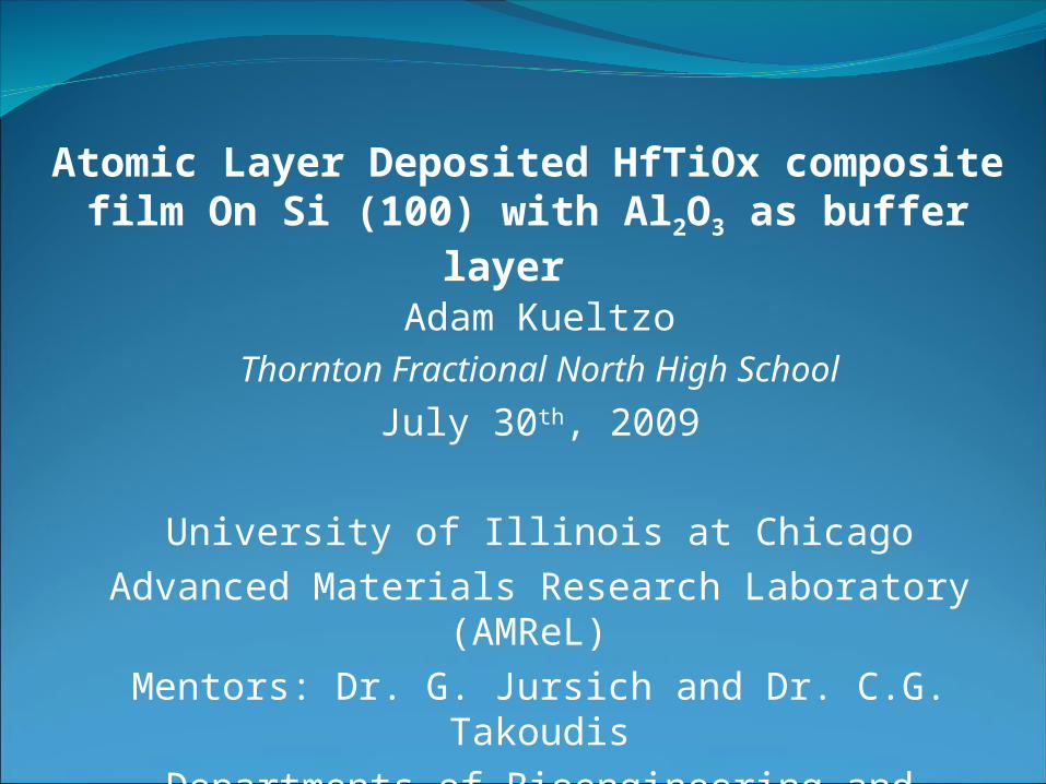
Adam KueltzoThornton Fractional North High School
July 30th, 2009
University of Illinois at ChicagoAdvanced Materials Research Laboratory
(AMReL) Mentors: Dr. G. Jursich and Dr. C.G. TakoudisDepartments of Bioengineering and Chemical
Engineering
Atomic Layer Deposited HfTiOx composite film On Si (100) with Al2O3 as
buffer layer
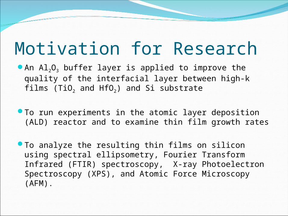
Motivation for ResearchAn Al2O3 buffer layer is applied to improve the quality
of the interfacial layer between high-k films (TiO2 and HfO2) and Si substrate
To run experiments in the atomic layer deposition (ALD) reactor and to examine thin film growth rates
To analyze the resulting thin films on silicon using spectral ellipsometry, Fourier Transform Infrared (FTIR) spectroscopy, X-ray Photoelectron Spectroscopy (XPS), and Atomic Force Microscopy (AFM).
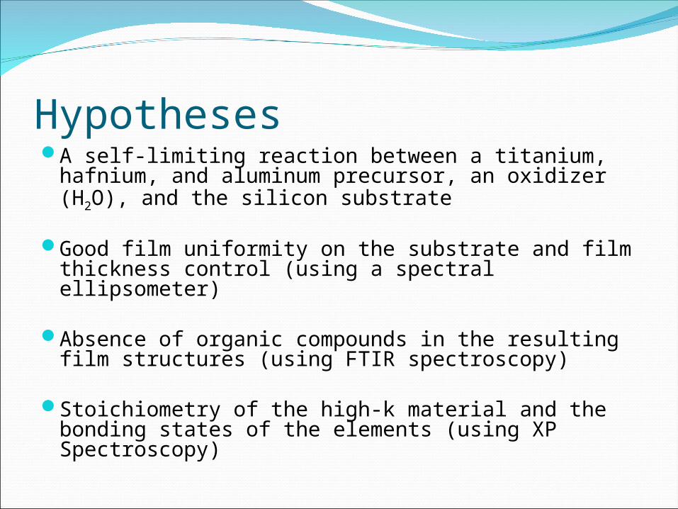
HypothesesA self-limiting reaction between a titanium,
hafnium, and aluminum precursor, an oxidizer (H2O), and the silicon substrate
Good film uniformity on the substrate and film thickness control (using a spectral ellipsometer)
Absence of organic compounds in the resulting film structures (using FTIR spectroscopy)
Stoichiometry of the high-k material and the bonding states of the elements (using XP Spectroscopy)
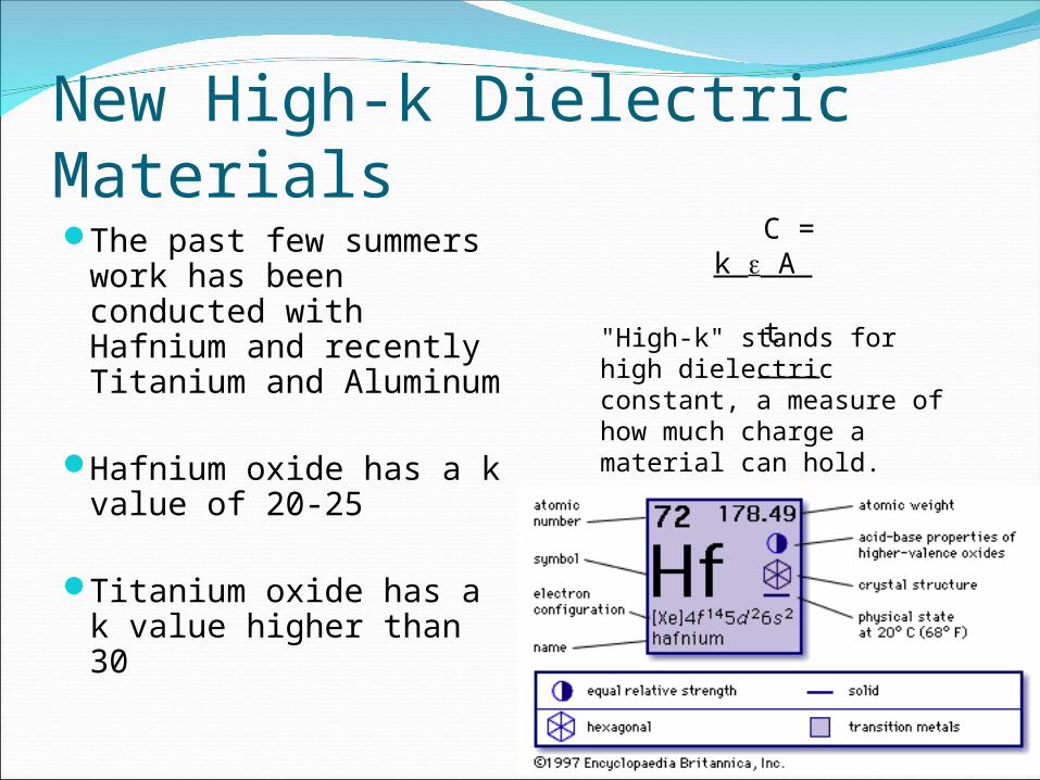
New High-k Dielectric MaterialsThe past few summers
work has been conducted with Hafnium and recently Titanium and Aluminum
Hafnium oxide has a k value of 20-25
Titanium oxide has a k value higher than 30
"High-k" stands for high dielectric constant, a measure of how much charge a material can hold.
C = k A
t

Why deposit multiple precursors on substrate?
Enhances dielectric constant (k)
Aids in the size miniaturization of semiconductor devices
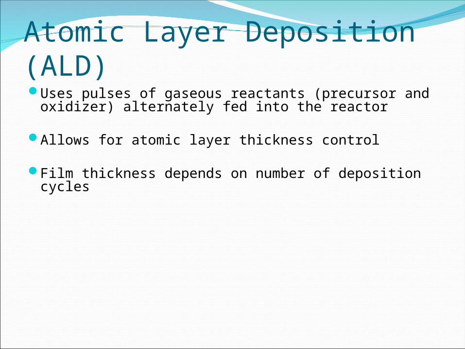
Atomic Layer Deposition (ALD)Uses pulses of gaseous reactants (precursor and
oxidizer) alternately fed into the reactor
Allows for atomic layer thickness control
Film thickness depends on number of deposition cycles

ALD Process“One Cycle”PrecursorPurge (N2)
Oxidizer (H2O)
Purge (N2)
http://www.cambridgenanotech.com/
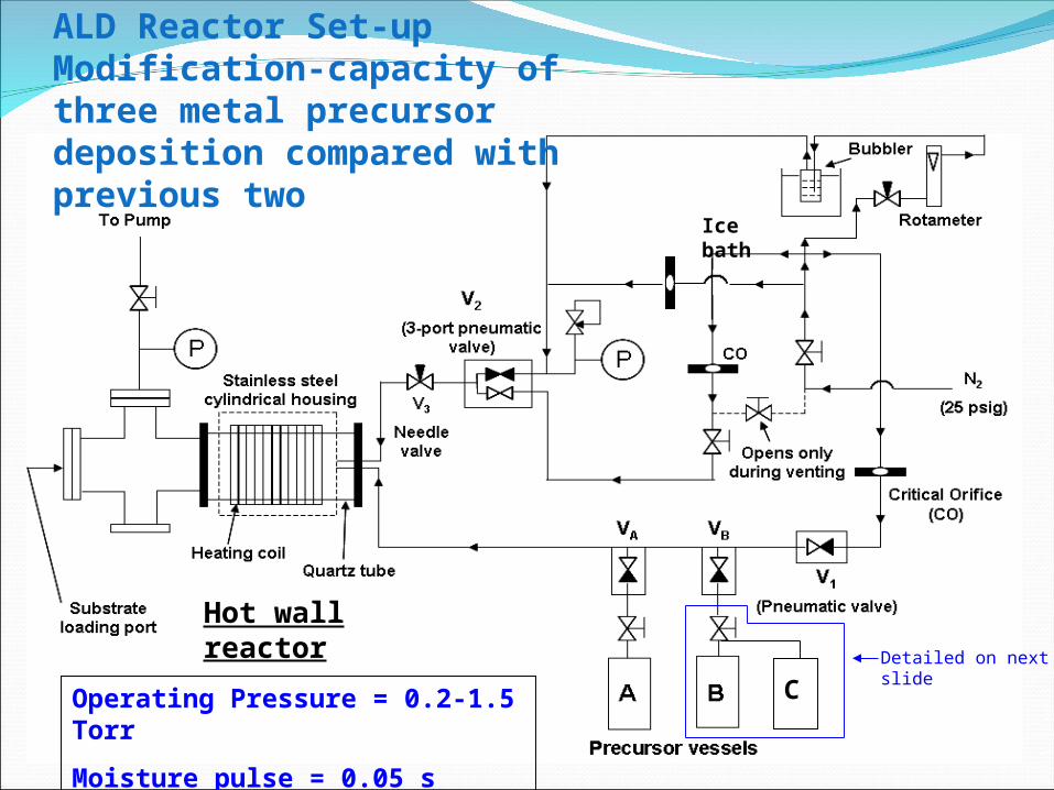
ALD Reactor Set-up Modification-capacity of three metal precursor deposition compared with previous two
Operating Pressure = 0.2-1.5 Torr
Moisture pulse = 0.05 s
Ice bath
Hot wall reactor
CDetailed on next slide
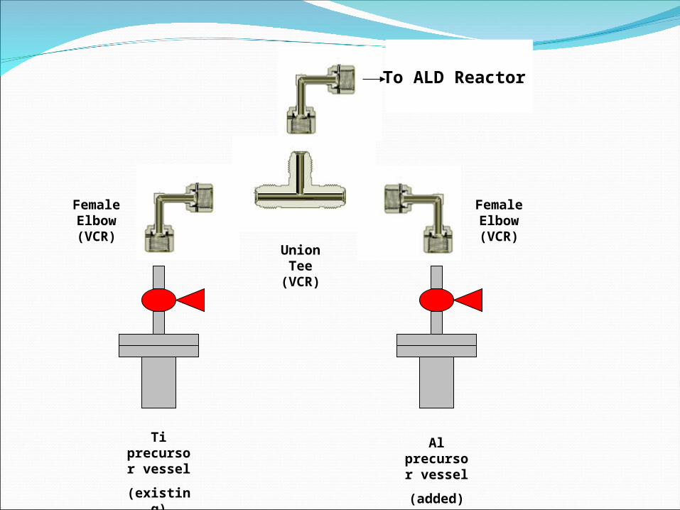
Union Tee (VCR)
Female Elbow (VCR)
Female Elbow (VCR)
Ti precursor
vessel
(existing)
Al precursor
vessel
(added)
To ALD Reactor
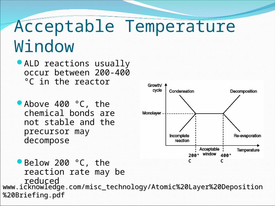
Acceptable Temperature WindowALD reactions usually
occur between 200-400 °C in the reactor
Above 400 °C, the chemical bonds are not stable and the precursor may decompose
Below 200 °C, the reaction rate may be reduced www.icknowledge.com/misc_technology/Atomic%20Layer%20Depositionwww.icknowledge.com/misc_technology/Atomic%20Layer%20Deposition
%20Briefing.pdf%20Briefing.pdf
200°C
400°C
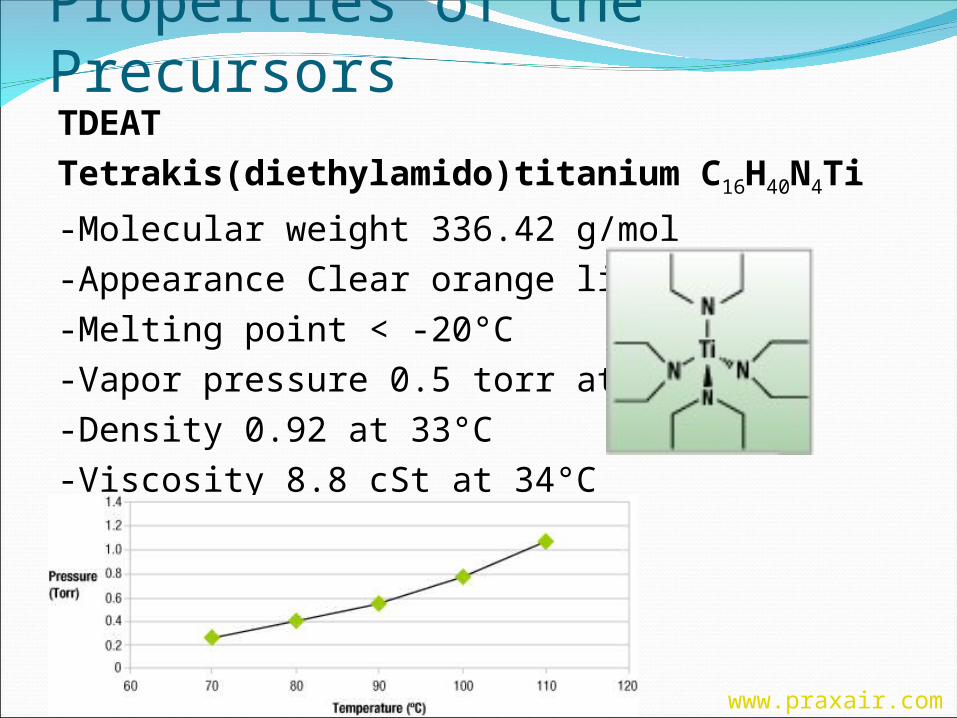
Properties of the PrecursorsTDEATTetrakis(diethylamido)titanium C16H40N4Ti
-Molecular weight 336.42 g/mol -Appearance Clear orange liquid -Melting point < -20°C -Vapor pressure 0.5 torr at 90°C -Density 0.92 at 33°C -Viscosity 8.8 cSt at 34°C
www.praxair.com
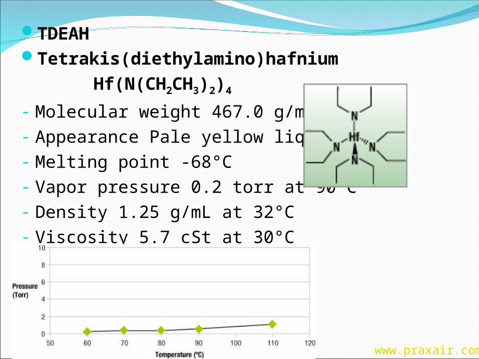
TDEAHTetrakis(diethylamino)hafnium Hf(N(CH2CH3)2)4
- Molecular weight 467.0 g/mol - Appearance Pale yellow liquid - Melting point -68°C - Vapor pressure 0.2 torr at 90°C - Density 1.25 g/mL at 32°C - Viscosity 5.7 cSt at 30°C
www.praxair.com

TDEAA Tris(diethylamino)aluminium
Al(N(C2H5)2)3
- Molecular Weight 486.7 g.mol-1
- Physical State Low MP solid - Melting Point 28-31°C - Boiling Point 250°C - Vapor Pressure 0.2 Torr @ 100°C - Density 0.915 g.cm-3 @ 25°C
www.aloha.airliquide.com
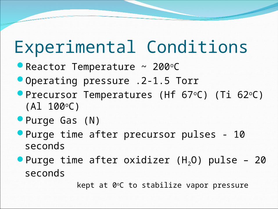
Experimental ConditionsReactor Temperature ~ 200oCOperating pressure .2-1.5 TorrPrecursor Temperatures (Hf 67oC) (Ti 62oC) (Al
100oC)Purge Gas (N) Purge time after precursor pulses - 10 secondsPurge time after oxidizer (H2O) pulse – 20
secondskept at 0oC to stabilize
vapor pressure
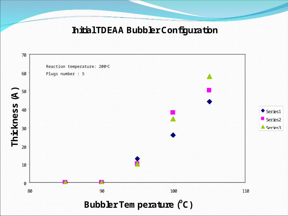
Initial TDEAA Bubbler Configuration
0
10
20
30
40
50
60
70
80 90 100 110
Bubbler Temperature (oC)
Th
ick
ne
ss
(A
)
Series1
Series2
Series3
Reaction temperature: 200oC
Plugs number : 5
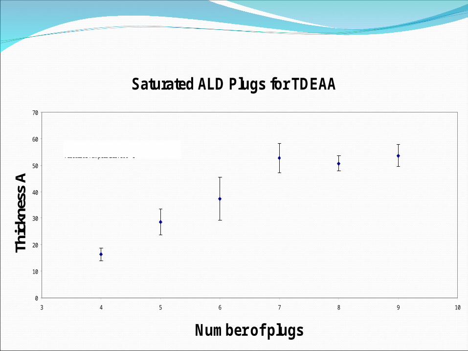
Saturated ALD Plugs for TDEAA
0
10
20
30
40
50
60
70
3 4 5 6 7 8 9 10
Number of plugs
Thic
knes
s A
Reaction Temperature: 225 ºCPrecursor Temperature: 100 ºC
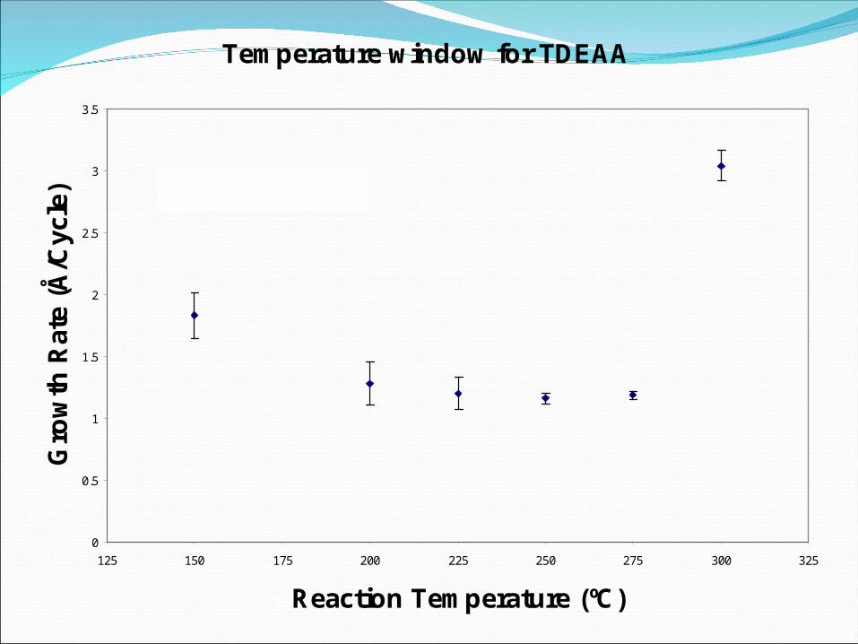
Temperature window for TDEAA
0
0.5
1
1.5
2
2.5
3
3.5
125 150 175 200 225 250 275 300 325
Reaction Temperature (ºC)
Gro
wth
Rat
e (Å
/Cyc
le) Precursor Temperature: 100 ºC
Plugs Number: 7

Growth Rate of HfO2 (at the Reaction T of 200 ºC)
0
20
40
60
80
100
120
140
0 25 50 75 100 125 150Cycle number
Th
ickn
ess
(An
gst
rom
)
Grow th Rate = 1Å/cycle
Future WorkFurther validate the deposition rate of
TDEAA - Thickness determinationDeposition of TDEAH and TDEATApply TDEAA buffer layer to silicon substrate

References
Anthony, J.M., Wallace, R.M., & Wilk, G.D. (2001). High-k Gate Dielectrics: Current Status and MaterialsProperties Considerations. Applied Physics Review, 89 , 5243-5275.
Brain, Marshall. (n.d.). How Semiconductors Work. [WWW page]. http://computer.howstuffworks.com/diode.htm.
Cambridge NanoTech, Inc. (2003-2007). Cambridge NanoTech: Atomic Layer Deposition Systems. [WWWpage].
http://www.cambridgenanotech.com/.
IC Knowledge LLC. (2004). Technology Backgrounder: Atomic Layer Deposition. [WWWpage]. http://www.icknowledge.com/misc_technology/Atomic%20Layer%20Deposition
%20Briefing.pdf.
Intel® Education. (n.d.) Inside The Intel® Manufacturing Process: How Transistors Work. [WWWpage].http://www.intel.com/education/transworks/index.htm. Majumder, P., Jursich, G., Kueltzo, A., & Takoudis, C. (2008). Atomic Layer Deposition of Y2O3 Films on
Silicon Using Tris(ethylcyclopentadienyl) Yttrium Precursor and Water Vapor. Journal of The Electrochemical Society. 155(8), G152-G158.
Mutschler, Ann Steffora. (2007). Intel, IBM Embrace High-k Gates for 45nm. Electronic News.
Peters, Laura. (2007). Behind the Breakdown of High-k Dielectrics.Semiconductor International. p. 30.
Praxair Technology, Inc. [WWWpage]. http://www.praxair.com
Zant, P. V. (2000). Microchip Fabrication (4th ed.). New York: McGraw Hill.
Air Liquide[WWWpage]. http://www.airliquide.com/en/semiconductors/aloha-advanced-precursors/high-k.html

Acknowledgements EEC-NSF Grant #0926260
Mentors: Dr. Greg Jursich and Dr. Christos Takoudis
Doctoral students: Qian Tao and Manish Singh