Embed Size (px)
Citation preview
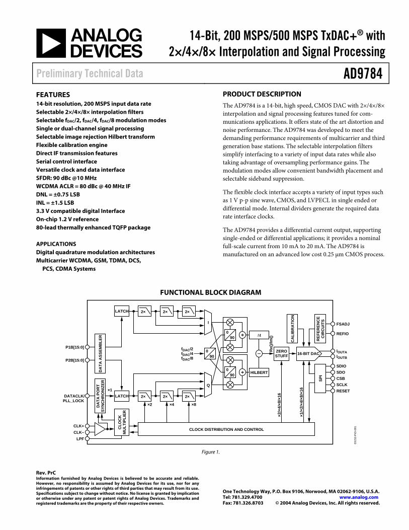
14-Bit, 200 MSPS/500 MSPS TxDAC+® with 2×/4×/8× Interpolation and Signal Processing
Preliminary Technical Data AD9784
Rev. PrC Information furnished by Analog Devices is believed to be accurate and reliable. However, no responsibility is assumed by Analog Devices for its use, nor for any infringements of patents or other rights of third parties that may result from its use. Specifications subject to change without notice. No license is granted by implication or otherwise under any patent or patent rights of Analog Devices. Trademarks and registered trademarks are the property of their respective owners.
One Technology Way, P.O. Box 9106, Norwood, MA 02062-9106, U.S.A. Tel: 781.329.4700 www.analog.com Fax: 781.326.8703 © 2004 Analog Devices, Inc. All rights reserved.
FEATURES 14-bit resolution, 200 MSPS input data rate Selectable 2×/4×/8× interpolation filters Selectable fDAC/2, fDAC/4, fDAC/8 modulation modes Single or dual-channel signal processing Selectable image rejection Hilbert transform Flexible calibration engine Direct IF transmission features Serial control interface Versatile clock and data interface SFDR: 90 dBc @10 MHz WCDMA ACLR = 80 dBc @ 40 MHz IF DNL = ±0.75 LSB INL = ±1.5 LSB 3.3 V compatible digital Interface On-chip 1.2 V reference 80-lead thermally enhanced TQFP package APPLICATIONS Digital quadrature modulation architectures Multicarrier WCDMA, GSM, TDMA, DCS, PCS, CDMA Systems
PRODUCT DESCRIPTION
The AD9784 is a 14-bit, high speed, CMOS DAC with 2×/4×/8× interpolation and signal processing features tuned for com-munications applications. It offers state of the art distortion and noise performance. The AD9784 was developed to meet the demanding performance requirements of multicarrier and third generation base stations. The selectable interpolation filters simplify interfacing to a variety of input data rates while also taking advantage of oversampling performance gains. The modulation modes allow convenient bandwidth placement and selectable sideband suppression.
The flexible clock interface accepts a variety of input types such as 1 V p-p sine wave, CMOS, and LVPECL in single ended or differential mode. Internal dividers generate the required data rate interface clocks.
The AD9784 provides a differential current output, supporting single-ended or differential applications; it provides a nominal full-scale current from 10 mA to 20 mA. The AD9784 is manufactured on an advanced low cost 0.25 µm CMOS process.
FUNCTIONAL BLOCK DIAGRAM
16-BIT DAC
REF
EREN
CE
CIR
CU
ITS
CA
LIB
RA
TIO
N
SPI
ZEROSTUFF
HILBERT
∆t0
90
090
090
Re(
)/Im
()
2×2×2×LATCH
CLO
CK
MU
LTIP
LIER
2×2×2×LATCH
Q
I
DA
TA A
SSEM
BLE
RD
ATA
PO
RT
SYN
CH
RO
NIZ
ER
fDAC/2fDAC/4fDAC/8
×1
×2 ×4 ×8
CLOCK DISTRIBUTION AND CONTROL
×2/×
4/×8
/×16
×1/×
2/×4
/×8/
×16
CLK+CLK–
LPF
DATACLK/PLL_LOCK
P2B[15:0]
P1B[15:0]
FSADJ
REFIO
IOUTAIOUTB
SDIOSDOCSBSCLKRESET
0315
2-Pr
D-0
01
Figure 1.
AD9784 Preliminary Technical Data
Rev. PrC | Page 2 of 52
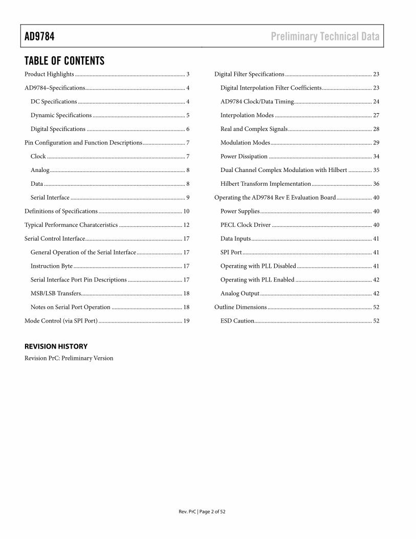
TABLE OF CONTENTS Product Highlights ........................................................................... 3
AD9784–Specifications.................................................................... 4
DC Specifications ......................................................................... 4
Dynamic Specifications ............................................................... 5
Digital Specifications ................................................................... 6
Pin Configuration and Function Descriptions............................. 7
Clock .............................................................................................. 7
Analog............................................................................................ 8
Data ................................................................................................ 8
Serial Interface .............................................................................. 9
Definitions of Specifications ......................................................... 10
Typical Performance Charatceristics ........................................... 12
Serial Control Interface.................................................................. 17
General Operation of the Serial Interface ............................... 17
Instruction Byte .......................................................................... 17
Serial Interface Port Pin Descriptions ..................................... 17
MSB/LSB Transfers..................................................................... 18
Notes on Serial Port Operation ................................................ 18
Mode Control (via SPI Port) ......................................................... 19
Digital Filter Specifications ........................................................... 23
Digital Interpolation Filter Coefficients.................................. 23
AD9784 Clock/Data Timing..................................................... 24
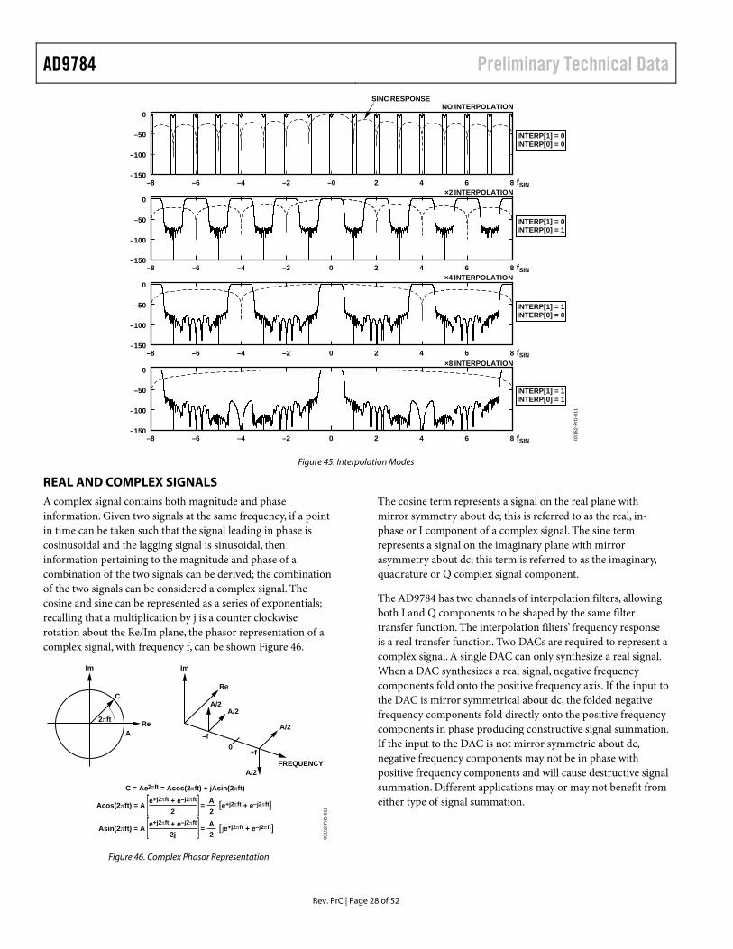
Interpolation Modes .................................................................. 27
Real and Complex Signals......................................................... 28
Modulation Modes..................................................................... 29
Power Dissipation ...................................................................... 34
Dual Channel Complex Modulation with Hilbert ................ 35
Hilbert Transform Implementation......................................... 36
Operating the AD9784 Rev E Evaluation Board........................ 40
Power Supplies ............................................................................ 40
PECL Clock Driver .................................................................... 40
Data Inputs.................................................................................. 41
SPI Port ........................................................................................ 41
Operating with PLL Disabled ................................................... 41
Operating with PLL Enabled .................................................... 42
Analog Output ............................................................................ 42
Outline Dimensions ....................................................................... 52
ESD Caution................................................................................ 52
REVISION HISTORY
Revision PrC: Preliminary Version

Preliminary Technical Data AD9784
Rev. PrC | Page 3 of 52
PRODUCT HIGHLIGHTS 1. The AD9784 is a member of a high speed interpolating
TxDAC+ family with 16-/14-/12-bit resolutions.
2. 2×/4×/8× user selectable interpolating filter eases data rate and output signal reconstruction filter requirements.
3. 200 MSPS input data rate.
4. Ultrahigh speed 500 MSPS DAC conversion rate.
5. Internal PLL/clock divider provides data rate clock for easy interfacing.
6. Flexible clock with single-ended or differential input: CMOS, 1 V p-p sine wave and LVPECL capability.
7. Complete CMOS DAC function operates from a 2.7 V to 3.6 V single analog (AVDD) supply and a 2.5 V (DVDD) digital supply. The DAC full-scale current can be reduced for lower power operation, and a sleep mode is provided for low-power idle periods.
8. On-chip voltage reference: The AD9784 includes a 1.20 V temperature-compensated band gap voltage reference.
AD9784 Preliminary Technical Data
Rev. PrC | Page 4 of 52
AD9784–SPECIFICATIONS DC SPECIFICATIONS Table 1. TMIN to TMAX, AVDD1, AVDD2 = 3.3 V, ACVDD, ADVDD, CLKVDD, DVDD, DRVDD = 2.5 V, IOUTFS = 20 mA, unless otherwise noted Parameter Min Typ Max Unit
RESOLUTION 14 Bits DC Accuracy1
Integral Nonlinearity 1.5 LSB Differential Nonlinearity 0.75 LSB
ANALOG OUTPUT Offset Error % of FSR
Gain Error (Without Internal Reference) % of FSR Gain Error (With Internal Reference) % of FSR Full-Scale Output Current2 10 20 mA Output Compliance Range –1.0 +1.0 V Output Resistance TBD kΩ Output Capacitance 3 pF
REFERENCE OUTPUT Reference Voltage 1.14 1.20 1.26 V Reference Output Current3 1 µA
REFERENCE INPUT Input Compliance Range 0.1 1.25 V Reference Input Resistance (Ext Reference Mode) 10 MΩ Small Signal Bandwith 0.5 MHz
TEMPERATURE COEFFICIENTS Unipolar Offset Drift ppm of FSR/°C Gain Drift (Without Internal Reference) ppm of FSR/°C Gain Drift (With Internal Reference) ppm of FSR/°C Reference Voltage Drift ppm /°C
POWER SUPPLY AVDD1, AVDD2
Voltage Range 3.1 3.3 3.5 V Analog Supply Current (IAVDD1) mA Analog Supply Current (IAVDD2) mA IAVDD1 in SLEEP Mode mA
ACVDD, ADVDD Voltage Range 2.35 2.5 2.65 V Analog Supply Current (IACVDD) mA Analog Supply Current (IADVDD) mA
CLKVDD Voltage Range 2.35 2.5 2.65 V Clock Supply Current (ICLKVDD) mA
DVDD Voltage Range 2.35 2.5 2.65 V Digital Supply Current (IDVDD) mA
DRVDD Voltage Range 2.35 2.5/3.3 3.5 V Digital Supply Current (IDRVDD) mA Nominal Power Dissipation4 1.25 W
OPERATING RANGE –40 +85 °C
1 Measured at IOUTA driving a virtual ground. 2 Nominal full-scale current, IOUTFS, is 32× the IREF current. 3 Use an external amplifier to drive any external load. 4 Measured under the following conditions: fDATA = 125 MSPS, fDAC = 500 MSPS, 4× Interpolation, fDAC/4 Modulation, Hilbert Off.
Preliminary Technical Data AD9784
Rev. PrC | Page 5 of 52
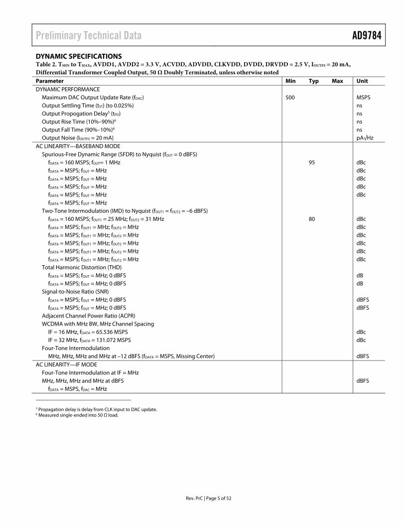
DYNAMIC SPECIFICATIONS Table 2. TMIN to TMAX, AVDD1, AVDD2 = 3.3 V, ACVDD, ADVDD, CLKVDD, DVDD, DRVDD = 2.5 V, IOUTFS = 20 mA, Differential Transformer Coupled Output, 50 Ω Doubly Terminated, unless otherwise noted Parameter Min Typ Max Unit DYNAMIC PERFORMANCE
Maximum DAC Output Update Rate (fDAC) 500 MSPS Output Settling Time (tST) (to 0.025%) ns Output Propogation Delay5 (tPD) ns Output Rise Time (10%–90%)6 ns Output Fall Time (90%–10%)6 ns Output Noise (IOUTFS = 20 mA) pA√Hz
AC LINEARITY—BASEBAND MODE Spurious-Free Dynamic Range (SFDR) to Nyquist (fOUT = 0 dBFS)
fDATA = 160 MSPS; fOUT= 1 MHz 95 dBc fDATA = MSPS; fOUT = MHz dBc fDATA = MSPS; fOUT = MHz dBc fDATA = MSPS; fOUT = MHz dBc fDATA = MSPS; fOUT = MHz dBc fDATA = MSPS; fOUT = MHz
Two-Tone Intermodulation (IMD) to Nyquist (fOUT1 = fOUT2 = –6 dBFS) fDATA = 160 MSPS; fOUT1 = 25 MHz; fOUT2 = 31 MHz 80 dBc fDATA = MSPS; fOUT1 = MHz; fOUT2 = MHz dBc fDATA = MSPS; fOUT1 = MHz; fOUT2 = MHz dBc fDATA = MSPS; fOUT1 = MHz; fOUT2 = MHz dBc fDATA = MSPS; fOUT1 = MHz; fOUT2 = MHz dBc fDATA = MSPS; fOUT1 = MHz; fOUT2 = MHz dBc
Total Harmonic Distortion (THD) fDATA = MSPS; fOUT = MHz; 0 dBFS dB fDATA = MSPS; fOUT = MHz; 0 dBFS dB
Signal-to-Noise Ratio (SNR) fDATA = MSPS; fOUT = MHz; 0 dBFS dBFS fDATA = MSPS; fOUT = MHz; 0 dBFS dBFS
Adjacent Channel Power Ratio (ACPR) WCDMA with MHz BW, MHz Channel Spacing
IF = 16 MHz, fDATA = 65.536 MSPS dBc IF = 32 MHz, fDATA = 131.072 MSPS dBc
Four-Tone Intermodulation MHz, MHz, MHz and MHz at –12 dBFS (fDATA = MSPS, Missing Center) dBFS
AC LINEARITY—IF MODE Four-Tone Intermodulation at IF = MHz MHz, MHz, MHz and MHz at dBFS dBFS
fDATA = MSPS, fDAC = MHz
5 Propagation delay is delay from CLK input to DAC update. 6 Measured single-ended into 50 Ω load.
AD9784 Preliminary Technical Data
Rev. PrC | Page 6 of 52
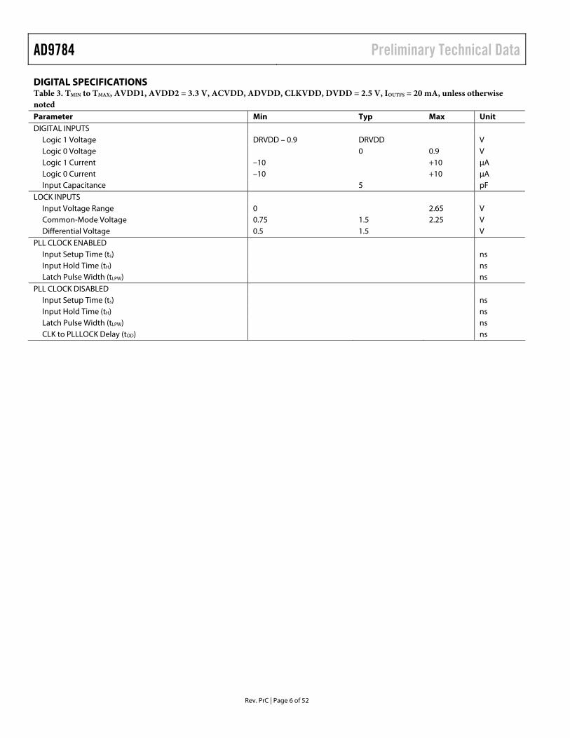
DIGITAL SPECIFICATIONS Table 3. TMIN to TMAX, AVDD1, AVDD2 = 3.3 V, ACVDD, ADVDD, CLKVDD, DVDD = 2.5 V, IOUTFS = 20 mA, unless otherwise noted Parameter Min Typ Max Unit DIGITAL INPUTS
Logic 1 Voltage DRVDD – 0.9 DRVDD V Logic 0 Voltage 0 0.9 V Logic 1 Current –10 +10 µA Logic 0 Current –10 +10 µA Input Capacitance 5 pF
LOCK INPUTS Input Voltage Range 0 2.65 V Common-Mode Voltage 0.75 1.5 2.25 V Differential Voltage 0.5 1.5 V
PLL CLOCK ENABLED Input Setup Time (ts) ns Input Hold Time (tH) ns Latch Pulse Width (tLPW) ns
PLL CLOCK DISABLED Input Setup Time (ts) ns Input Hold Time (tH) ns Latch Pulse Width (tLPW) ns CLK to PLLLOCK Delay (tOD) ns
Preliminary Technical Data AD9784
Rev. PrC | Page 7 of 52
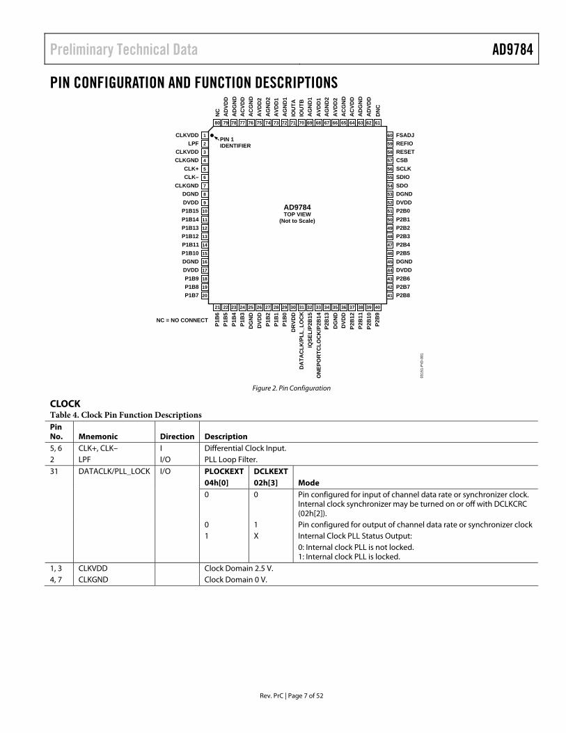
PIN CONFIGURATION AND FUNCTION DESCRIPTIONS
80 79 78 77 76 71 70 69 68 67 66 6575 74 73 72 64 63 62 61
16
1
2
3
4
5
6
7
8
9
10
11
13
14
15
12
17
18
20
19
21 22 23 24 25 26 27 28 29 30 31 32 33 34 35 36 37 38 39 40
PIN 1IDENTIFIER
60
59
58
57
56
55
54
53
52
51
50
49
48
47
46
45
44
43
42
41
NC = NO CONNECT
NC
AD
VDD
AD
GN
DA
CVD
DA
CG
ND
AVD
D2
AG
ND
2A
VDD
1A
GN
D1
IOU
TAIO
UTB
AG
ND
1A
VDD
1A
GN
D2
AVD
D2
AC
GN
DA
CVD
DA
DG
ND
AD
VDD
DN
C
CLKVDDLPF
CLKVDDCLKGND
CLK+CLK–
CLKGNDDGNDDVDDP1B15P1B14P1B13P1B12P1B11P1B10DGNDDVDDP1B9P1B8P1B7
FSADJREFIORESETCSBSCLKSDIOSDODGNDDVDDP2B0P2B1P2B2P2B3P2B4P2B5DGND
P1B
6P1
B5
P1B
4P1
B3
DG
ND
DVD
DP1
B2
P1B
1P1
B0
DR
VDD
IQSE
L/P2
B15
ON
EPO
RTC
LOC
K/P
2B14
P2B
13D
GN
DD
VDD
DA
TAC
LK/P
LL_L
OC
K
AD9784TOP VIEW
(Not to Scale)
DVDDP2B6P2B7P2B8
P2B
12P2
B11
P2B
10P2
B9
0315
1-Pr
D-0
01
Figure 2. Pin Configuration
CLOCK Table 4. Clock Pin Function Descriptions Pin No. Mnemonic Direction Description 5, 6 CLK+, CLK– I Differential Clock Input. 2 LPF I/O PLL Loop Filter.
PLOCKEXT 04h[0]
DCLKEXT 02h[3] Mode
0 0 Pin configured for input of channel data rate or synchronizer clock. Internal clock synchronizer may be turned on or off with DCLKCRC (02h[2]).
0 1 Pin configured for output of channel data rate or synchronizer clock
31 DATACLK/PLL_LOCK I/O
1 X Internal Clock PLL Status Output: 0: Internal clock PLL is not locked. 1: Internal clock PLL is locked.
1, 3 CLKVDD Clock Domain 2.5 V. 4, 7 CLKGND Clock Domain 0 V.
AD9784 Preliminary Technical Data
Rev. PrC | Page 8 of 52
ANALOG Table 5. Analog Pin Function Descriptions Pin No. Mnemonic Direction Description 59 REFIO A Reference. 60 FSADJ A Full-Scale Adjust. 70, 71 IOUTB, IOUTA A Differential DAC Output Currents. 61 DNC Do not connect. 62, 79 ADVDD Analog Domain Digital Content 2.5 V. 63, 78 ADGND Analog Domain Digital Content 0 V. 64, 77 ACVDD Analog Domain Clock Content 2.5 V. 65, 76 ACGND Analog Domain Clock Content 0 V. 66, 75 AVDD2 Analog Domain Clock Switching 3.3 V. 67, 74 AGND2 Analog Domain Switching 0 V. 68, 73 AVDD1 Analog Domain Quiet 3.3 V. 69, 72 AGND1 Analog Domain Quiet 0 V.
DATA Table 6. Data Pin Function Descriptions Pin No. Mnemonic Direction Description
Input Data Port One.
ONEPORT 02h[6] Mode 0 Latched Data Routed for 1 Channel Processing.
10–15, 18–24, 27–29
P1B15–P1B0 I
1 Latched Data Demultiplexed by IQSEL and Routed for Interleaved I/Q Processing.
ONEPORT 02h[6]
IQPOL 02h[1]
IQSEL/ P2B15 Mode (IQPOL == 0)
0 X X Latched data routed to Q channel bit 15(MSB) processing.
1 0 0 Latched data on data port one routed to Q channel processing.
1 0 1 Latched data on data port one routed to I channel processing.
1 1 0 Latched data on data port one routed to I channel processing.
32 IQSEL/P2B15 I
1 1 1 Latched data on data port one routed to Q channel processing.
ONEPORT 02h[6] 0 Latched data routed for Q channel Bit 14 processing.
33 ONEPORTCLK/P2B14 I/O
1 Pin configured for output of clock at twice the channel data route. 34, 37–43, 46–51
P2B13–P2B0 I Input Data Port Two Bits 13–0.
30 DRVDD Digital Output Pin Supply, 2.5 V or 3.3 V. 9, 17, 26, 36, 44, 52
DVDD Digital Domain 2.5 V.
8, 16, 25, 35, 45, 53
DGND Digital Domain 0 V.
Preliminary Technical Data AD9784
Rev. PrC | Page 9 of 52
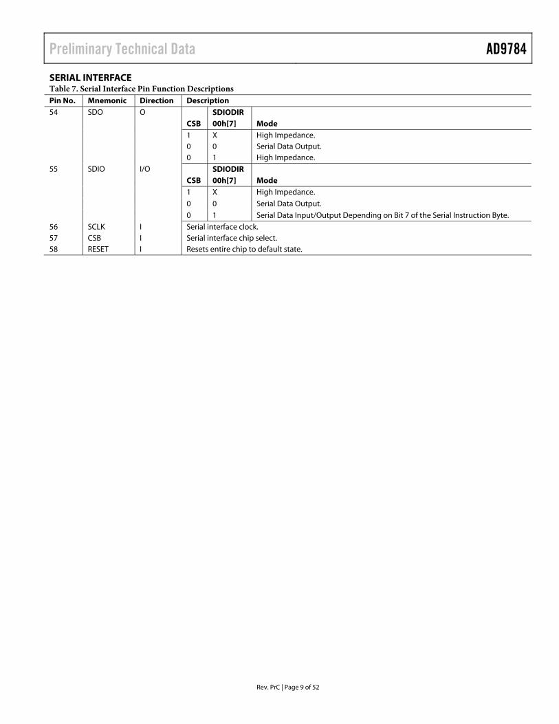
SERIAL INTERFACE Table 7. Serial Interface Pin Function Descriptions Pin No. Mnemonic Direction Description
CSB SDIODIR 00h[7] Mode
1 X High Impedance. 0 0 Serial Data Output.
54 SDO O
0 1 High Impedance.
CSB SDIODIR 00h[7] Mode
1 X High Impedance. 0 0 Serial Data Output.
55 SDIO I/O
0 1 Serial Data Input/Output Depending on Bit 7 of the Serial Instruction Byte. 56 SCLK I Serial interface clock. 57 CSB I Serial interface chip select. 58 RESET I Resets entire chip to default state.
AD9784 Preliminary Technical Data
Rev. PrC | Page 10 of 52
DEFINITIONS OF SPECIFICATIONS Linearity Error (Integral Nonlinearity or INL)
Linearity error is defined as the maximum deviation of the actual analog output from the ideal output, determined by a straight line drawn from zero to full scale.
Differential Nonlinearity (or DNL)
DNL is the measure of the variation in analog value, normalized to full scale, associated with a 1 LSB change in digital input code.
Monotonicity
A D/A converter is monotonic if the output either increases or remains constant as the digital input increases.
Offset Error
The deviation of the output current from the ideal of zero is called offset error. For IOUTA, 0 mA output is expected when the inputs are all 0s. For IOUTB, 0 mA output is expected when all inputs are set to 1s.
Gain Error
The difference between the actual and ideal output span. The actual span is determined by the output when all inputs are set to 1s, minus the output when all inputs are set to 0s.
Output Compliance Range
The range of allowable voltage at the output of a current-output DAC. Operation beyond the maximum compliance limits may cause either output stage saturation or breakdown, resulting in nonlinear performance.
Temperature Drift
Temperature drift is specified as the maximum change from the ambient (+25°C) value to the value at either TMIN or TMAX. For offset and gain drift, the drift is reported in ppm of full-scale range (FSR) per degree C. For reference drift, the drift is reported in ppm per degree C.
Power Supply Rejection
The maximum change in the full-scale output as the supplies are varied from minimum to maximum specified voltages.
Settling Time
The time required for the output to reach and remain within a specified error band about its final value, measured from the start of the output transition.
Glitch Impulse
Asymmetrical switching times in a DAC give rise to undesired output transients that are quantified by a glitch impulse. It is specified as the net area of the glitch in pV-s.
Spurious-Free Dynamic Range
The difference, in dB, between the rms amplitude of the output signal and the peak spurious signal over the specified bandwidth.
Total Harmonic Distortion
THD is the ratio of the rms sum of the first six harmonic components to the rms value of the measured fundamental. It is expressed as a percentage or in decibels (dB).
Signal-to-Noise Ratio (SNR)
S/N is the ratio of the rms value of the measured output signal to the rms sum of all other spectral components below the Nyquist frequency, excluding the first six harmonics and dc. The value for SNR is expressed in decibels.
Interpolation Filter
If the digital inputs to the DAC are sampled at a multiple rate of fDATA (interpolation rate), a digital filter can be constructed which has a sharp transition band near fDATA/2. Images which would typically appear around fDAC (output data rate) can be greatly suppressed.
Pass-Band
Frequency band in which any input applied therein passes unattenuated to the DAC output.
Stop-Band Rejection
The amount of attenuation of a frequency outside the pass-band applied to the DAC, relative to a full-scale signal applied at the DAC input within the pass-band.
Group Delay
Number of input clocks between an impulse applied at the device input and peak DAC output current. A half-band FIR filter has constant group delay over its entire frequency range
Impulse Response
Response of the device to an impulse applied to the input.

Preliminary Technical Data AD9784
Rev. PrC | Page 11 of 52
Adjacent Channel Power Ratio (or ACPR)
A ratio in dBc between the measured power within a channel relative to its adjacent channel.
Complex Modulation
The process of passing the real and imaginary components of a signal through a complex modulator (transfer function = ejwt = coswt + jsinwt) and realizing real and imaginary components on the modulator output.
Complex Image Rejection
In a traditional two part upconversion, two images are created around the second IF frequency. These images are redundant and have the effect of wasting transmitter power and system bandwidth. By placing the real part of a second complex modulator in series with the first complex modulator, either the upper or lower frequency image near the second IF can be rejected.
AD9784 Preliminary Technical Data
Rev. PrC | Page 12 of 52
TYPICAL PERFORMANCE CHARATCERISTICS (TMIN to TMAX, AVDD1, AVDD2 = 3.3 V, ACVDD, ADVDD, CLKVDD, DVDD, DRVDD = 2.5 V, IOUTFS = 20 mA, Differential Transformer Coupled Output, 50 Ω Doubly Terminated, unless otherwise noted)
TBD–000
–000
–000
–000
–000
–000 –000 –000 –000 –000ALL CAPS (Initial caps)
ALL
CA
PS (I
nitia
l cap
s)
Figure 3 Single-Tone Spectrum@ FDATA = 65 MSPS With FOUT = FDATA/3
TBD–000
–000
–000
–000
–000
–000 –000 –000 –000 –000ALL CAPS (Initial caps)
ALL
CA
PS (I
nitia
l cap
s)
Figure 4. In-Band SFDR vs. FOUT @ FDATA = 65 MSPS
TBD–000
–000
–000
–000
–000
–000 –000 –000 –000 –000ALL CAPS (Initial caps)
ALL
CA
PS (I
nitia
l cap
s)
Figure 5. Out-of-Band SFDR vs. FOUT @ FDATA = 65 MSPS
TBD–000
–000
–000
–000
–000
–000 –000 –000 –000 –000ALL CAPS (Initial caps)
ALL
CA
PS (I
nitia
l cap
s)
Figure 6. Single-Tone Spectrum @ FDATA = 78 MSPS with FOUT = FDATA/3
TBD–000
–000
–000
–000
–000
–000 –000 –000 –000 –000ALL CAPS (Initial caps)
ALL
CA
PS (I
nitia
l cap
s)
Figure 7. In-Band SFDR Vs. FOUT @ FDATA = 78 MSPS
TBD–000
–000
–000
–000
–000
–000 –000 –000 –000 –000ALL CAPS (Initial caps)
ALL
CA
PS (I
nitia
l cap
s)
Figure 8. Out-of-Band SFDR vs. FOUT @ FDATA = 78 MSPS
Preliminary Technical Data AD9784
Rev. PrC | Page 13 of 52
TBD–000
–000
–000
–000
–000
–000 –000 –000 –000 –000ALL CAPS (Initial caps)
ALL
CA
PS (I
nitia
l cap
s)
Figure 9. Single-Tone Spectrum @ FDATA = 160 MSPS with FOUT = FDATA/3
TBD–000
–000
–000
–000
–000
–000 –000 –000 –000 –000ALL CAPS (Initial caps)
ALL
CA
PS (I
nitia
l cap
s)
Figure 10. In-Band SFDR vs. FOUT @ FDATA = 160 MSPS
TBD–000
–000
–000
–000
–000
–000 –000 –000 –000 –000ALL CAPS (Initial caps)
ALL
CA
PS (I
nitia
l cap
s)
Figure 11. Out-of-Band SFDR vs. FOUT @ FDATA = 160 MSPS
TBD–000
–000
–000
–000
–000
–000 –000 –000 –000 –000ALL CAPS (Initial caps)
ALL
CA
PS (I
nitia
l cap
s)
Figure 12. Third Order IMD Products vs. FOUT @ FDATA = 65 MSPS
TBD–000
–000
–000
–000
–000
–000 –000 –000 –000 –000ALL CAPS (Initial caps)
ALL
CA
PS (I
nitia
l cap
s)
Figure 13. Third Order IMD Products vs. FOUT @ FDATA = 78 MSPS
TBD–000
–000
–000
–000
–000
–000 –000 –000 –000 –000ALL CAPS (Initial caps)
ALL
CA
PS (I
nitia
l cap
s)
Figure 14. Third Order IMD Products vs. FOUT @ FDATA = 160 MSPS
AD9784 Preliminary Technical Data
Rev. PrC | Page 14 of 52
TBD–000
–000
–000
–000
–000
–000 –000 –000 –000 –000ALL CAPS (Initial caps)
ALL
CAPS
(Ini
tial c
aps)
Figure 15. TPC 13. Third Order IMD Products vs. FOUT and Interpolation Rate
1× – FDATA = 160 MSPS
2× – FDATA = 160 MSPS
4× – FDATA = 80 MSPS
8× – FDATA = 50 MSPS
TBD–000
–000
–000
–000
–000
–000 –000 –000 –000 –000ALL CAPS (Initial caps)
ALL
CAPS
(Ini
tial c
aps)
Figure 16. Third Order IMD Products vs. AOUT and Interpolation Rate FDATA = 50 MSPS for All Cases
1× – FDAC = 50 MSPS
2× – FDAC = 100 MSPS
4× – FDAC = 200 MSPS
8× – FDAC = 400 MSPS
TBD–000
–000
–000
–000
–000
–000 –000 –000 –000 –000ALL CAPS (Initial caps)
ALL
CA
PS (I
nitia
l cap
s)
Figure 17. SFDR vs. AVDD @ FOUT = 10 MHz; FDAC = 320 MSPS FDATA = 160 MSPS
TBD–000
–000
–000
–000
–000
–000 –000 –000 –000 –000ALL CAPS (Initial caps)
ALL
CAPS
(Ini
tial c
aps)
Figure 18. 3rd Order IMD Products vs. AVDD @ FOUT = 10 MHz, FDAC = 320 MSPS, FDATA = 160 MSPS
TBD–000
–000
–000
–000
–000
–000 –000 –000 –000 –000ALL CAPS (Initial caps)
ALL
CAPS
(Ini
tial c
aps)
Figure 19. SNR vs. Data Rate for fOUT = 5 MHz
TBD–000
–000
–000
–000
–000
–000 –000 –000 –000 –000ALL CAPS (Initial caps)
ALL
CAPS
(Ini
tial c
aps)
Figure 20. SFDR vs. Temperature @ fOUT = fDATA/11
Preliminary Technical Data AD9784
Rev. PrC | Page 15 of 52
TBD–000
–000
–000
–000
–000
–000 –000 –000 –000 –000ALL CAPS (Initial caps)
ALL
CA
PS (I
nitia
l cap
s)
Figure 21. Single Tone Spurious Performance, fOUT = 10 MHz, fDATA = 150 MSPS, No Interpolation
TBD–000
–000
–000
–000
–000
–000 –000 –000 –000 –000ALL CAPS (Initial caps)
ALL
CA
PS (I
nitia
l cap
s)
Figure 22. Two Tone IMD Performance, FDATA = 150 MSPS, No Interpolation
TBD–000
–000
–000
–000
–000
–000 –000 –000 –000 –000ALL CAPS (Initial caps)
ALL
CA
PS (I
nitia
l cap
s)
Figure 23. Single Tone Spurious Performance, FOUT = 10 MHz, FDATA = 150 MSPS, Interpolation = 2×
TBD–000
–000
–000
–000
–000
–000 –000 –000 –000 –000ALL CAPS (Initial caps)
ALL
CA
PS (I
nitia
l cap
s)
Figure 24. Two Tone IMD Performance, FDATA = 90 MSPS, Interpolation = 4×
TBD–000
–000
–000
–000
–000
–000 –000 –000 –000 –000ALL CAPS (Initial caps)
ALL
CA
PS (I
nitia
l cap
s)
Figure 25. Single Tone Spurious Performance, FOUT = 10 MHz, FDATA = 80 MSPS, Interpolation = 4×
TBD–000
–000
–000
–000
–000
–000 –000 –000 –000 –000ALL CAPS (Initial caps)
ALL
CA
PS (I
nitia
l cap
s)
Figure 26. Two Tone IMD Performance, FOUT = 10 MHz, FDATA = 50 MSPS, Interpolation = 8×
AD9784 Preliminary Technical Data
Rev. PrC | Page 16 of 52
TBD–000
–000
–000
–000
–000
–000 –000 –000 –000 –000ALL CAPS (Initial caps)
ALL
CA
PS (I
nitia
l cap
s)
Figure 27. Single Tone Spurious Performance, FOUT = 10 MHz, FDATA = 50 MSPS, Interpolation = 8×
TBD–000
–000
–000
–000
–000
–000 –000 –000 –000 –000ALL CAPS (Initial caps)
ALL
CA
PS (I
nitia
l cap
s)
Figure 28. Eight Tone IMD Performance, FDATA = 160 MSPS, Interpolation = 8×
Preliminary Technical Data AD9784
Rev. PrC | Page 17 of 52
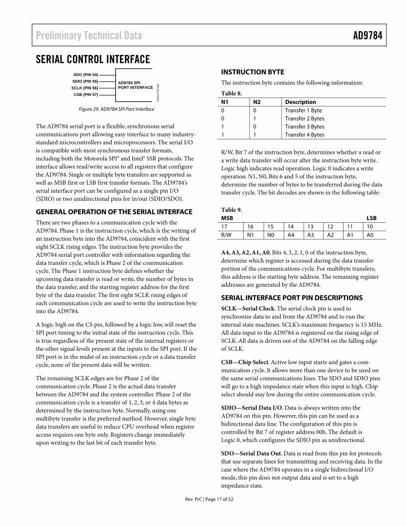
SERIAL CONTROL INTERFACE
AD9784 SPIPORT INTERFACE
SDO (PIN 54)SDIO (PIN 55)
SCLK (PIN 56)CSB (PIN 57)
0315
1-Pr
D-0
02
Figure 29. AD9784 SPI Port Interface
The AD9784 serial port is a flexible, synchronous serial communications port allowing easy interface to many industry-standard microcontrollers and microprocessors. The serial I/O is compatible with most synchronous transfer formats, including both the Motorola SPI® and Intel® SSR protocols. The interface allows read/write access to all registers that configure the AD9784. Single or multiple byte transfers are supported as well as MSB first or LSB first transfer formats. The AD9784’s serial interface port can be configured as a single pin I/O (SDIO) or two unidirectional pins for in/out (SDIO/SDO).
GENERAL OPERATION OF THE SERIAL INTERFACE There are two phases to a communication cycle with the AD9784. Phase 1 is the instruction cycle, which is the writing of an instruction byte into the AD9784, coincident with the first eight SCLK rising edges. The instruction byte provides the AD9784 serial port controller with information regarding the data transfer cycle, which is Phase 2 of the communication cycle. The Phase 1 instruction byte defines whether the upcoming data transfer is read or write, the number of bytes in the data transfer, and the starting register address for the first byte of the data transfer. The first eight SCLK rising edges of each communication cycle are used to write the instruction byte into the AD9784.
A logic high on the CS pin, followed by a logic low, will reset the SPI port timing to the initial state of the instruction cycle. This is true regardless of the present state of the internal registers or the other signal levels present at the inputs to the SPI port. If the SPI port is in the midst of an instruction cycle or a data transfer cycle, none of the present data will be written.
The remaining SCLK edges are for Phase 2 of the communication cycle. Phase 2 is the actual data transfer between the AD9784 and the system controller. Phase 2 of the communication cycle is a transfer of 1, 2, 3, or 4 data bytes as determined by the instruction byte. Normally, using one multibyte transfer is the preferred method. However, single byte data transfers are useful to reduce CPU overhead when register access requires one byte only. Registers change immediately upon writing to the last bit of each transfer byte.
INSTRUCTION BYTE The instruction byte contains the following information:
Table 8. N1 N2 Description 0 0 Transfer 1 Byte 0 1 Transfer 2 Bytes 1 0 Transfer 3 Bytes 1 1 Transfer 4 Bytes
R/W, Bit 7 of the instruction byte, determines whether a read or a write data transfer will occur after the instruction byte write. Logic high indicates read operation. Logic 0 indicates a write operation. N1, N0, Bits 6 and 5 of the instruction byte, determine the number of bytes to be transferred during the data transfer cycle. The bit decodes are shown in the following table:
Table 9. MSB LSB 17 16 15 14 13 12 11 10 R/W N1 N0 A4 A3 A2 A1 A0
A4, A3, A2, A1, A0, Bits 4, 3, 2, 1, 0 of the instruction byte, determine which register is accessed during the data transfer portion of the communications cycle. For multibyte transfers, this address is the starting byte address. The remaining register addresses are generated by the AD9784.
SERIAL INTERFACE PORT PIN DESCRIPTIONS SCLK—Serial Clock. The serial clock pin is used to synchronize data to and from the AD9784 and to run the internal state machines. SCLK’s maximum frequency is 15 MHz. All data input to the AD9784 is registered on the rising edge of SCLK. All data is driven out of the AD9784 on the falling edge of SCLK.
CSB—Chip Select. Active low input starts and gates a com-munication cycle. It allows more than one device to be used on the same serial communications lines. The SDO and SDIO pins will go to a high impedance state when this input is high. Chip select should stay low during the entire communication cycle.
SDIO—Serial Data I/O. Data is always written into the AD9784 on this pin. However, this pin can be used as a bidirectional data line. The configuration of this pin is controlled by Bit 7 of register address 00h. The default is Logic 0, which configures the SDIO pin as unidirectional.
SDO—Serial Data Out. Data is read from this pin for protocols that use separate lines for transmitting and receiving data. In the case where the AD9784 operates in a single bidirectional I/O mode, this pin does not output data and is set to a high impedance state.
AD9784 Preliminary Technical Data
Rev. PrC | Page 18 of 52
MSB/LSB TRANSFERS The AD9784 serial port can support both most significant bit (MSB) first or least significant bit (LSB) first data formats. This functionality is controlled by register address DATADIR (00h[6]). The default is MSB first. When this bit is set active high, the AD9784 serial port is in LSB first format. That is, if the AD9784 is in LSB first mode, the instruction byte must be written from least significant bit to most significant bit. Multibyte data transfers in MSB format can be completed by writing an instruction byte that includes the register address of the most significant byte. In MSB first mode, the serial port internal byte address generator decrements for each byte required of the multibyte communication cycle. Multibyte data transfers in LSB first format can be completed by writing an instruction byte that includes the register address of the least significant byte. In LSB first mode, the serial port internal byte address generator increments for each byte required of the multibyte communication cycle.
The AD9784 serial port controller address will increment from 1Fh to 00h for multibyte I/O operations if the MSB first mode is active. The serial port controller address will decrement from 00h to 1Fh for multibyte I/O operations if the LSB first mode is active.
NOTES ON SERIAL PORT OPERATION The AD9784 serial port configuration bits reside in Bits 6 and 7 of register address 00h. It is important to note that the configuration changes immediately upon writing to the last bit of the register. For multibyte transfers, writing to this register may occur during the middle of communication cycle. Care must be taken to compensate for this new configuration for the remaining bytes of the current communication cycle.
The same considerations apply to setting the software reset, SWRST (00h[5]) bit. All other registers are set to their default values but the software reset doesn’t affect the bits in register address 00h and 04h.
It is recommended to use only single byte transfers when changing serial port configurations or initiating a software reset.
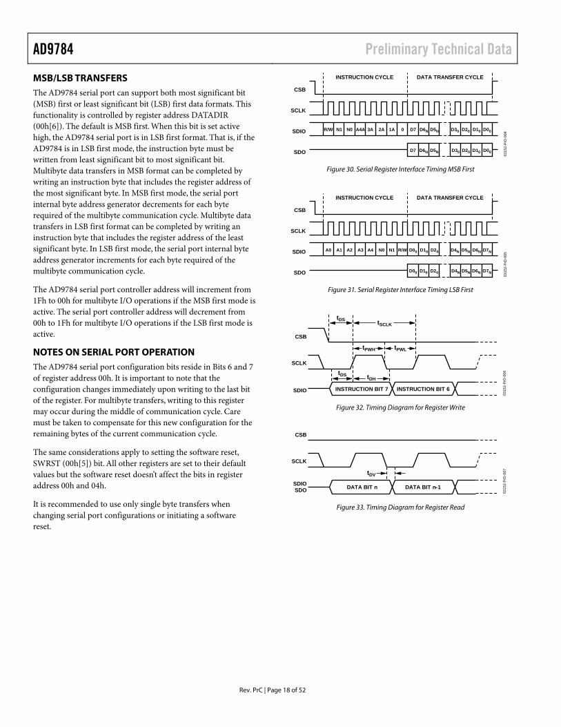
R/W N1 N0 A4A 3A 2A 1A 0 D7 D6N D5N D00D10D20D30
D7 D6N D5N D00D10D20D30
INSTRUCTION CYCLE DATA TRANSFER CYCLE
CSB
SCLK
SDIO
SDO 0315
2-Pr
D-0
04
Figure 30. Serial Register Interface Timing MSB First
A0 A1 A2 A3 A4 N0 N1 R/W D00 D10 D20 D7ND6ND5ND4N
D00 D10 D20 D7ND6ND5ND4N
INSTRUCTION CYCLE DATA TRANSFER CYCLE
CSB
SCLK
SDIO
SDO 0315
2-Pr
D-0
05
Figure 31. Serial Register Interface Timing LSB First
INSTRUCTION BIT 6INSTRUCTION BIT 7
CSB
SCLK
SDIO
tDS
tDS tDH
tPWH tPWL
tSCLK
0315
2-Pr
D-0
06
Figure 32. Timing Diagram for Register Write
DATA BIT n–1DATA BIT n
CSB
SCLK
SDIOSDO 03
152-
PrD
-007tDV
Figure 33. Timing Diagram for Register Read
Preliminary Technical Data AD9784
Rev. PrC | Page 19 of 52
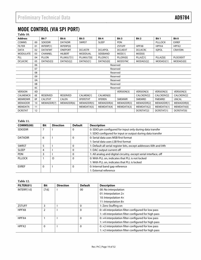
MODE CONTROL (VIA SPI PORT) Table 10. Address Bit 7 Bit 6 Bit 5 Bit 4 Bit 3 Bit 2 Bit 1 Bit 0
COMMS 00 SDIODIR DATADIR SWRST SLEEP PDN PLLLOCK EXREF
FILTER 01 INTERP[1] INTERP[0] ZSTUFF HPFX8 HPFX4 HPFX2
DATA 02 DATAFMT ONEPORT DCLKSTR DCLKPOL DCLKEXT DCLKCRC IQPOL CRAYDIN
MODULATE 03 CHANNEL HILBERT MODDUAL SIDEBAND MOD[1] MOD[0]
PLL 04 PLLON PLLMULT[1] PLLMULT[0] PLLDIV[1] PLLDIV[0] PLLAZ[1] PLLAZ[0] PLOCKEXT
DCLKCRC 05 DATADJ[3] DATADJ[2] DATADJ[1] DATADJ[0] MODSYNC MODADJ[2] MODADJ[1] MODADJ[0]
06 Reserved
07 Reserved
08 Reserved
09 Reserved
0A Reserved
0B Reserved
0C Reserved
VERSION 0D VERSION[3] VERSION[3] VERSION[3] VERSION[3]
CALMEMCK 0E RESERVED RESERVED CALMEM[1] CALMEN[0] CALCKDIV[2] CALCKDIV[2] CALCKDIV[2]
MEMRDWR 0F CALSTAT CALEN XFERSTAT XFEREN SMEMWR SMEMRD FMEMRD UNCAL
MEMADDR 10 MEMADDR[7] MEMADDR[6] MEMADDR[5] MEMADDR[4] MEMADDR[3] MEMADDR[2] MEMADDR[1] MEMADDR[0]
MEMDATA 11 MEMDATA[5] MEMDATA[4] MEMDATA[3] MEMDATA[2] MEMDATA[1] MEMDATA[0]
DCRSTAT 12 DCRSTAT[2] DCRSTAT[1] DCRSTAT[0]
Table 11. COMMS(00) Bit Direction Default Description SDIODIR 7 I 0 0: SDIO pin configured for input only during data transfer
1: SDIO configured for input or output during data transfer DATADIR 6 I 0 0: Serial data uses MSB first format
1: Serial data uses LSB first format SWRST 5 I 0 1: Default all serial register bits, except addresses 00h and 04h SLEEP 4 I 0 1: DAC output current off PDN 3 I 0 1: All analog and digital circuitry, except serial interface, off PLLOCK 1 O 0 0: With PLL on, indicates that PLL is not locked
1: With PLL on, indicates that PLL is locked EXREF 0 I 0 0: Internal band gap reference
1: External reference
Table 12. FILTER(01) Bit Direction Default Description INTERP[1:0] [7:6] I 00 00: No interpolation
01: Interpolation 2× 10: Interpolation 4× 11: Interpolation 8×
ZSTUFF 3 I 0 1: Zero Stuffing on HPFX8 2 I 0 0: ×8 interpolation filter configured for low pass
1: ×8 interpolation filter configured for high pass HPFX4 1 I 0 0: ×4 interpolation filter configured for low pass
1: ×4 interpolation filter configured for high pass HPFX2 0 I 0 0: ×2 interpolation filter configured for low pass
1: ×2 interpolation filter configured for high pass
AD9784 Preliminary Technical Data
Rev. PrC | Page 20 of 52
Table 13. DATA(02) Bit Direction Default Description DATAFMT 7 I 0 0: Twos complement data format
1: Unsigned binary input data format ONEPORT 6 I 0 0: I and Q input data onto ports one and two respectively
1: I and Q input data interleaved onto port one DCLKSTR 5 I 0 0: DATACLK pin 12 mA drive strength
1: DATACLK pin 24 mA drive strength DCLKPOL 4 I 0 0: Input data latched on DATACLK rising edge
1: Input data latched on DATACLK falling edge DCLKEXT 3 I 0 0: With PLOCKEXT off, DATACLK pin inputs channel data rate or modulator synchronizer clock
1: With PLOCKEXT off, DATACLK pin outputs channel data rate or modulator synchronizer clock DCLKCRC 2 I 0 0: With PLOCKEXT off, and DATACLK pin as input, DATACLK clock recovery off
1: With PLOCKEXT off, and DATACLK pin as input, DATACLK clock recovery on IQPOL 1 I 0 0: In one port mode, IQSEL = 1 latches data into I channel, IQSEL = 0 latches data into Q channel
1: In one port mode, IQSEL = 0 latches data into I channel, IQSEL = 1 latches data into Q channel GRAYDIN 0 I 0 0: Gray decoder off
1: Gray decoder on
Table 14. MODULATE(03) Bit Direction Default Description
MODDUAL 03h [5]
CHANNEL 03h[7]
0 0 I channel processing routed to DAC 0 1 Q channel processing routed to DAC 1 0 Modulator real output routed to DAC
CHANNEL 7 I 0
1 1 Modulator imaginary output routed to DAC HILBERT 6 I 0 1: With MODDUAL on, Hilbert transform on MODDUAL 5 I 0 0: Modulator uses a single channel
1: Modulator uses both I and Q channels SIDEBAND 4 I 0 0: With MODDUAL on, lower sideband rejected
1: With MODDUAL on, upper sideband rejected MOD[1:0] [3:2] I 00 00: No modulation
01: fS/2 modulation 10: fS /4 modulation 11: fS /8 modulation
Preliminary Technical Data AD9784
Rev. PrC | Page 21 of 52
Table 15. PLL(04) Bit Direction Default Description PLLON 7 I 0 0: PLL off
1: PLL on PLLMULTI[1:0] [6:5] I 00 PLL MULTIPLY FACTOR
00: ×2 00: ×4 00: ×8 00: ×16
PLLDIV[1:0] [4:3] I 00 PLLMULT rate divide factor 00:/1 00:/2 00:/4 00:/8
PLLAZBW[1:0] [2:1] I 00 PLL Autozero settling bandwidth as fraction of CLK ±rate 00: /8 (lowest) 01: /4 10: /2 (highest)
PLOCKEXT 0 I 0 0: With PLL on, DATACLK/PLL_LOCK pin configured for DATACLK input/output 1: With PLL on, DATACLK/PLL_LOCK pin configured for output of PLLLOCK
Table 16. DCLKCRC(05) Bit Direction Default Description DATADJ[3:0] [7:4] I 0000 DATACLK offset. Twos complement respresentation
0111: +7 : 0000: 0 : 1000: -8
MODSYNC 3 I 00 0: With PLOCKEXT off, channel data rate clock synchronizer mode 1: With PLOCKEXT off, state machine clock synchronizer mode fS/8 fS/4 fS/2 000 1 1 1 001 1/√2 0 –1 010 0 –1 1 011 –1/√2 0 –1 100 –1 1 1 101 –1/√2 0 –1 110 0 –1 1
MODADJ[2:0] [2:0] I 000
111 1/√2 0 –1
Modulator coefficient offset
Table 17. VERSION(0D) Bit Direction Default Description VERSION[3:0] [3:0] O – Hardware version identifier
AD9784 Preliminary Technical Data
Rev. PrC | Page 22 of 52
Table 18. CALMEMCK(OE) Bit Direction Default Description CALMEM [5:4] O 00 Calibration memory
00: Uncalibrated 01: Self Calibration 10: Factory calibration 11: User input
CALCKDIV[2:0] [2:0] I 00 Calibration clock divide ratio from channel data rate 000: /32 001: /64 : 110: /2048 111: /4096
Table 19. MEMRDWR(OF) Bit Direction Default Description CALSTAT 7 O 0 0: Self Calibration cycle not complete
1: Self Calibration cycle complete CALEN 6 I 0 1: Self Calibration in progress XFERSTAT 5 O 0 0: Factory memory transfer not complete
1: Factory memory transfer complete XFEREN 4 I 0 1: Factory memory transfer in progress SMEMWR 3 I 0 1: Write static memory data from external port SMEMRD 2 I 0 1: Read static memory to external port FMEMRD 1 I 0 1: Read factory memory data to external port UNCAL 0 I 0 1: Use uncalibrated
Table 20. MEMADDR(10) Bit Direction Default Description MEMADDR [7:0] [7:0] I/O 00000000 Address of factory or static memory to be accessed
Table 21. MEMDATA(11) Bit Direction Default Description MEMDATA [5:0] [5:0] I/O 000000 Data or factory or static memory access
Table 22. DCRCSTAT(12) Bit Direction Default Description DCRCSTAT (2) 2 O 0 0: With DATACLK CRC on, lock has never been achieved
1: With DATACLK CRC on, lock has been achieved at least once DCRCSTAT(1) 1 O 0 0: With DATACLK CRC on, system is currently not locked
1: With DATACLK CRC on, system is currently locked DCRCSTAT(0) 0 O 0 0: With DATACLK CRC on, system is currently locked
1: With DATACLK CRC on, system lost lock due to jitter
Preliminary Technical Data AD9784
Rev. PrC | Page 23 of 52
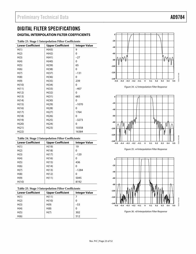
DIGITAL FILTER SPECIFICATIONS DIGITAL INTERPOLATION FILTER COEFFICIENTS
Table 23. Stage 1 Interpolation Filter Coefficients Lower Coefficient Upper Coefficient Integer Value H(1) H(43) 9 H(2) H(42) 0 H(3) H(41) –27 H(4) H(40) 0 H(5) H(39) 65 H(6) H(38) 0 H(7) H(37) –131 H(8) H(36) 0 H(9) H(35) 239 H(10) H(34) 0 H(11) H(33) –407 H(12) H(32) 0 H(13) H(31) 665 H(14) H(30) 0 H(15) H(29) –1070 H(16) H(28) 0 H(17) H(27) 1764 H(18) H(26) 0 H(19) H(25) –3273 H(20) H(24) 0 H(21) H(23) 10358 H(22) 16384
Table 24. Stage 2 Interpolation Filter Coefficients Lower Coefficient Upper Coefficient Integer Value H(1) H(19) 19 H(2) H(18) 0 H(3) H(17) –120 H(4) H(16) 0 H(5) H(15) 436 H(6) H(14) 0 H(7) H(13) –1284 H(8) H(12) 0 H(9) H(11) 5045 H(10) 8192
Table 25. Stage 3 Interpolation Filter Coefficients Lower Coefficient Upper Coefficient Integer Value H(1) H(11) 7 H(2) H(10) 0 H(3) H(9) –53 H(4) H(8) 0 H(5) H(7) 302 H(6) 512
0315
2-Pr
D-0
08
0.5–0.5 –0.4 –0.3 –0.2 –0.1 0 0.1 0.2 0.3 0.4–140
0
–20
–40
–60
–80
–100
–120
Figure 34. ×2 Interpolation Filter Response
0315
2-Pr
D-0
09
0.5–0.5 –0.4 –0.3 –0.2 –0.1 0 0.1 0.2 0.3 0.4–140
0
–20
–40
–60
–80
–100
–120
Figure 35. ×4 Interpolation Filter Response
0315
2-Pr
D-0
10
0.5–0.5 –0.4 –0.3 –0.2 –0.1 0 0.1 0.2 0.3 0.4–140
0
–20
–40
–60
–80
–100
–120
Figure 36. ×8 Interpolation Filter Response
AD9784 Preliminary Technical Data
Rev. PrC | Page 24 of 52
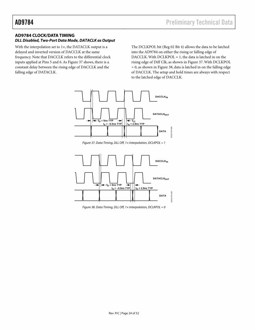
AD9784 CLOCK/DATA TIMING DLL Disabled, Two-Port Data Mode, DATACLK as Output
With the interpolation set to 1×, the DATACLK output is a delayed and inverted version of DACCLK at the same frequency. Note that DACCLK refers to the differential clock inputs applied at Pins 5 and 6. As Figure 37 shows, there is a constant delay between the rising edge of DACCLK and the falling edge of DATACLK.
The DCLKPOL bit (Reg 02 Bit 4) allows the data to be latched into the AD9784 on either the rising or falling edge of DACCLK. With DCLKPOL = 1, the data is latched in on the rising edge of Diff Clk, as shown in Figure 37. With DCLKPOL = 0, as shown in Figure 38, data is latched in on the falling edge of DACCLK. The setup and hold times are always with respect to the latched edge of DACCLK.
0315
2-Pr
D-0
66
DACCLKIN
DATACLKOUT
DATA
t12tD = 5ns TYPtH = 2.9ns TYPtS = –0.5ns TYP
Figure 37. Data Timing, DLL Off, 1× Interpolation, DCLKPOL = 1
0315
2-Pr
D-0
67
DACCLKIN
DATACLKOUT
DATA
tD = 6ns TYPtH = 2.9ns TYPtS = –0.5ns TYP
Figure 38. Data Timing, DLL Off, 1× Interpolation, DCLKPOL = 0
Preliminary Technical Data AD9784
Rev. PrC | Page 25 of 52
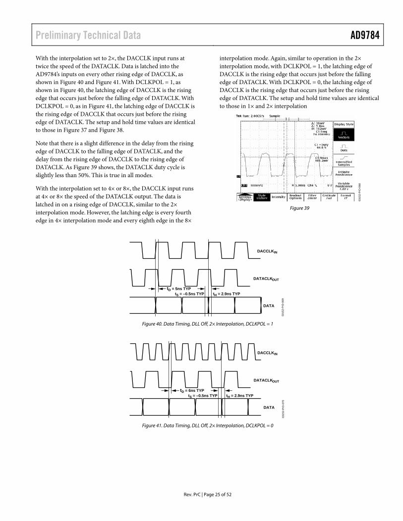
With the interpolation set to 2×, the DACCLK input runs at twice the speed of the DATACLK. Data is latched into the AD9784’s inputs on every other rising edge of DACCLK, as shown in Figure 40 and Figure 41. With DCLKPOL = 1, as shown in Figure 40, the latching edge of DACCLK is the rising edge that occurs just before the falling edge of DATACLK. With DCLKPOL = 0, as in Figure 41, the latching edge of DACCLK is the rising edge of DACCLK that occurs just before the rising edge of DATACLK. The setup and hold time values are identical to those in Figure 37 and Figure 38.
Note that there is a slight difference in the delay from the rising edge of DACCLK to the falling edge of DATACLK, and the delay from the rising edge of DACCLK to the rising edge of DATACLK. As Figure 39 shows, the DATACLK duty cycle is slightly less than 50%. This is true in all modes.
With the interpolation set to 4× or 8×, the DACCLK input runs at 4× or 8× the speed of the DATACLK output. The data is latched in on a rising edge of DACCLK, similar to the 2× interpolation mode. However, the latching edge is every fourth edge in 4× interpolation mode and every eighth edge in the 8×
interpolation mode. Again, similar to operation in the 2× interpolation mode, with DCLKPOL = 1, the latching edge of DACCLK is the rising edge that occurs just before the falling edge of DATACLK. With DCLKPOL = 0, the latching edge of DACCLK is the rising edge that occurs just before the rising edge of DATACLK. The setup and hold time values are identical to those in 1× and 2× interpolation
0315
2-Pr
D-0
68
Figure 39
0315
2-Pr
D-0
69
DACCLKIN
DATACLKOUT
DATA
tD = 5ns TYPtH = 2.9ns TYPtS = –0.5ns TYP
Figure 40. Data Timing, DLL Off, 2× Interpolation, DCLKPOL = 1
0315
2-Pr
D-0
70
DACCLKIN
DATACLKOUT
DATA
tD = 6ns TYPtH = 2.9ns TYPtS = –0.5ns TYP
Figure 41. Data Timing, DLL Off, 2× Interpolation, DCLKPOL = 0
AD9784 Preliminary Technical Data
Rev. PrC | Page 26 of 52
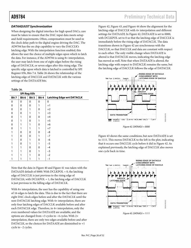
DATAADJUST Synchronization
When designing the digital interface for high speed DACs, care must be taken to ensure that the DAC input data meets setup-and-hold requirements. Often, compensation must be used in the clock delay path to the digital engine driving the DAC. The AD9784 has the on chip capability to vary the DACCLK’s latching edge. With the interpolation function enabled, this allows the user the choice of multiple edges upon which to latch the data. For instance, if the AD9784 is using 8× interpolation, the user may latch from one of eight edges before the rising edge of DATACLK, or seven edges after this rising edge. The specific edge upon which data is latched is controlled by SPI Register 05h, Bits 7:4. Table 26 shows the relationship of the latching edge of DACCLK and DATACLK with the various settings of the DATAADJ bits.
Table 26.
SPI Reg 05h Bit 7 Bit 6 Bit 5 Bit 4 Latching Edge wrt DATACLK
0 0 0 0 0 0 0 0 1 +1 0 0 1 0 +2 0 0 1 1 +3 0 1 0 0 +4 0 1 0 1 +5 0 1 1 0 +6 0 1 1 1 +7 1 0 0 0 –8 1 0 0 1 –7 1 0 1 0 –6 1 0 1 1 –5 1 1 0 0 –4 1 1 0 1 –3 1 1 1 0 –2 1 1 1 1 –1
Note that the data in Figure 40 and Figure 41 was taken with the DATAADJ default of 0000. With DCLKPOL = 0, the latching edge of DACCLK is just previous to the rising edge of DATACLK; with DCLKPOL = 1, the latching edge of DACCLK is just previous to the falling edge of DATACLK.
With 8× interpolation, the user has the capability of using one of 16 edges to latch the data. This is due to the fact that there are eight DAC clock edges before and after the DATACLK until the next DATACLK latching edge. With 4× interpolation, there are only four latching edges of DACCLK available before and after each DATACLK edge. Therefore, in 4× interpolation, only the even numbered values for DATAADJ are available, and the options are changed from +3 cycles to –4 cycles. With 2× interpolation, there are only two edges available before and after DATACLK, so the choices for DATAADJ are diminished to +1 cycle to –2 cycles.
Figure 42, Figure 43, and Figure 44 show the alignment for the latching edge of DACCLK with 4× interpolation and different settings for DATAADJ. In Figure 42, DATAADJ is set to 0000, with DCLKPOL set to 0 so that the latching edge of DACCLK is immediately before the rising edge of DATACLK. The data transitions shown in Figure 42 are synchronous with the DACCLK, so that DACCLK and data are constant with respect to each other. The only visible change when DATAADJ is altered is that DATACLK moves, indicating the latching edge has moved as well. Note that when DATAADJ is altered, the latching edge with respect to DATACLK remains the same, but the latching edge of DACCLK follows the edge of DATACLK.
0315
2-Pr
D-0
71
RISING EDGE OF DATACLKCONCURRENT WITHLATCHING EDGE OF DACCLK
DATA TRANSITION
DACCLKLATCHING EDGE
Figure 42. DATAADJ = 0000
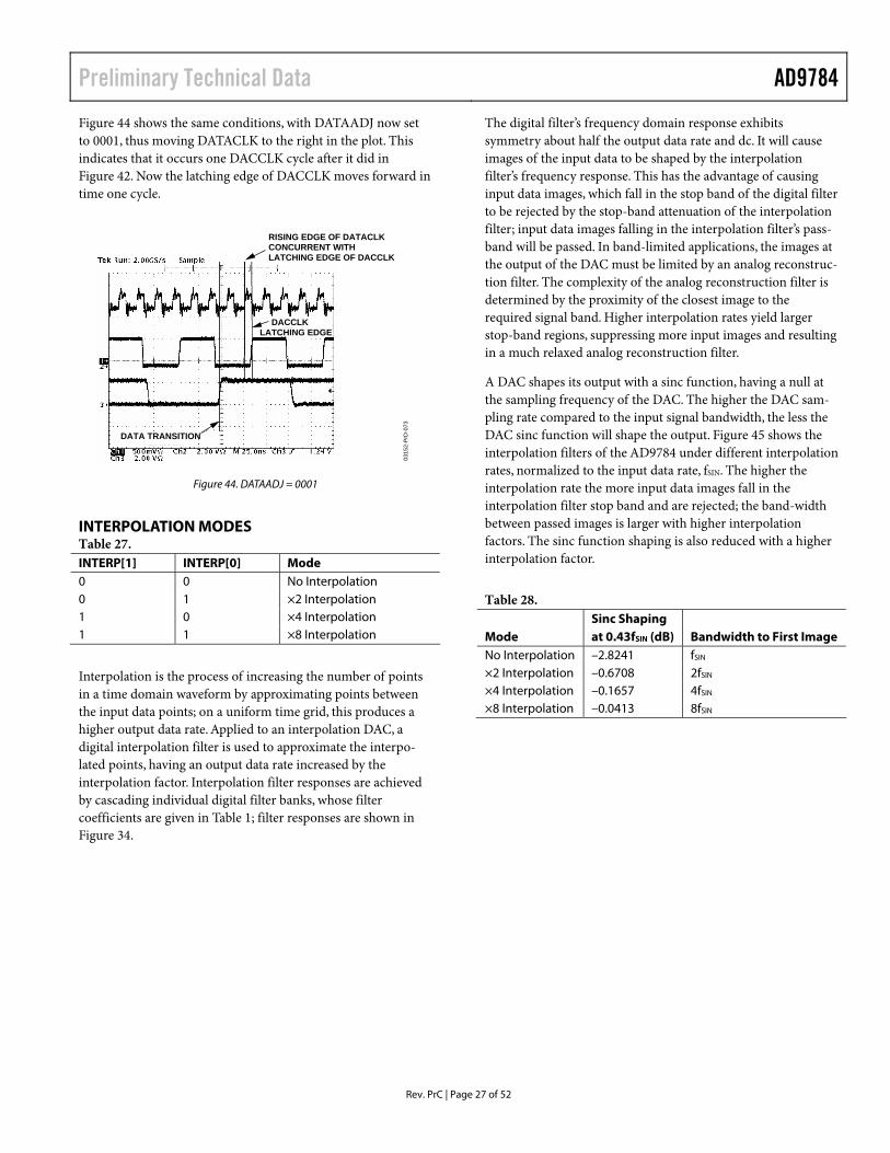
Figure 43 shows the same conditions, but now DATAADJ is set to 1111. This moves DATACLK to the left in the plot, indicating that it occurs one DACCLK cycle before it did in Figure 42. As explained previously, the latching edge of DACCLK also moves one cycle back in time.
0315
2-Pr
D-0
72
RISING EDGE OF DATACLKCONCURRENT WITHLATCHING EDGE OF DACCLK
DATA TRANSITION
DACCLKLATCHING EDGE
Figure 43. DATAADJ = 1111
Preliminary Technical Data AD9784
Rev. PrC | Page 27 of 52
Figure 44 shows the same conditions, with DATAADJ now set to 0001, thus moving DATACLK to the right in the plot. This indicates that it occurs one DACCLK cycle after it did in Figure 42. Now the latching edge of DACCLK moves forward in time one cycle.
0315
2-Pr
D-0
73
RISING EDGE OF DATACLKCONCURRENT WITHLATCHING EDGE OF DACCLK
DATA TRANSITION
DACCLKLATCHING EDGE
Figure 44. DATAADJ = 0001
INTERPOLATION MODES Table 27. INTERP[1] INTERP[0] Mode 0 0 No Interpolation 0 1 ×2 Interpolation 1 0 ×4 Interpolation 1 1 ×8 Interpolation
Interpolation is the process of increasing the number of points in a time domain waveform by approximating points between the input data points; on a uniform time grid, this produces a higher output data rate. Applied to an interpolation DAC, a digital interpolation filter is used to approximate the interpo-lated points, having an output data rate increased by the interpolation factor. Interpolation filter responses are achieved by cascading individual digital filter banks, whose filter coefficients are given in Table 1; filter responses are shown in Figure 34.
The digital filter’s frequency domain response exhibits symmetry about half the output data rate and dc. It will cause images of the input data to be shaped by the interpolation filter’s frequency response. This has the advantage of causing input data images, which fall in the stop band of the digital filter to be rejected by the stop-band attenuation of the interpolation filter; input data images falling in the interpolation filter’s pass-band will be passed. In band-limited applications, the images at the output of the DAC must be limited by an analog reconstruc-tion filter. The complexity of the analog reconstruction filter is determined by the proximity of the closest image to the required signal band. Higher interpolation rates yield larger stop-band regions, suppressing more input images and resulting in a much relaxed analog reconstruction filter.
A DAC shapes its output with a sinc function, having a null at the sampling frequency of the DAC. The higher the DAC sam-pling rate compared to the input signal bandwidth, the less the DAC sinc function will shape the output. Figure 45 shows the interpolation filters of the AD9784 under different interpolation rates, normalized to the input data rate, fSIN. The higher the interpolation rate the more input data images fall in the interpolation filter stop band and are rejected; the band-width between passed images is larger with higher interpolation factors. The sinc function shaping is also reduced with a higher interpolation factor.
Table 28.
Mode Sinc Shaping at 0.43fSIN (dB) Bandwidth to First Image
No Interpolation –2.8241 fSIN ×2 Interpolation –0.6708 2fSIN ×4 Interpolation –0.1657 4fSIN ×8 Interpolation –0.0413 8fSIN
AD9784 Preliminary Technical Data
Rev. PrC | Page 28 of 52
–8 –6 –4 –2 –0 2 4 6 8–150
–100
–50
0
–8 –6 –4 –2 0 2 4 6 8–150
–100
–50
0
–8 –6 –4 –2 0 2 4 6 8–150
–100
–50
0
–8 –6 –4 –2 0 2 4 6 8–150
–100
–50
0
NO INTERPOLATION
×4 INTERPOLATION
×2 INTERPOLATION
×8 INTERPOLATION
SINC RESPONSE
fSIN
fSIN
fSIN
fSIN
INTERP[1] = 1INTERP[0] = 1
INTERP[1] = 1INTERP[0] = 0
INTERP[1] = 0INTERP[0] = 1
INTERP[1] = 0INTERP[0] = 0
0315
2-Pr
D-0
11
Figure 45. Interpolation Modes
REAL AND COMPLEX SIGNALS A complex signal contains both magnitude and phase information. Given two signals at the same frequency, if a point in time can be taken such that the signal leading in phase is cosinusoidal and the lagging signal is sinusoidal, then information pertaining to the magnitude and phase of a combination of the two signals can be derived; the combination of the two signals can be considered a complex signal. The cosine and sine can be represented as a series of exponentials; recalling that a multiplication by j is a counter clockwise rotation about the Re/Im plane, the phasor representation of a complex signal, with frequency f, can be shown Figure 46.
Im
Re
CRe
Im
A/2A/2
A/2
A/2
FREQUENCY
0+f
–fA
2πft
C = Ae2πft = Acos(2πft) + jAsin(2πft)
Acos(2πft) = A = [e+j2πft + e–j2πft]e+j2πft + e–j2πft
2A2
Asin(2πft) = A = [je+j2πft + e–j2πft]e+j2πft + e–j2πft
2jA2 03
152-
PrD
-012
Figure 46. Complex Phasor Representation
The cosine term represents a signal on the real plane with mirror symmetry about dc; this is referred to as the real, in-phase or I component of a complex signal. The sine term represents a signal on the imaginary plane with mirror asymmetry about dc; this term is referred to as the imaginary, quadrature or Q complex signal component.
The AD9784 has two channels of interpolation filters, allowing both I and Q components to be shaped by the same filter transfer function. The interpolation filters’ frequency response is a real transfer function. Two DACs are required to represent a complex signal. A single DAC can only synthesize a real signal. When a DAC synthesizes a real signal, negative frequency components fold onto the positive frequency axis. If the input to the DAC is mirror symmetrical about dc, the folded negative frequency components fold directly onto the positive frequency components in phase producing constructive signal summation. If the input to the DAC is not mirror symmetric about dc, negative frequency components may not be in phase with positive frequency components and will cause destructive signal summation. Different applications may or may not benefit from either type of signal summation.
Preliminary Technical Data AD9784
Rev. PrC | Page 29 of 52
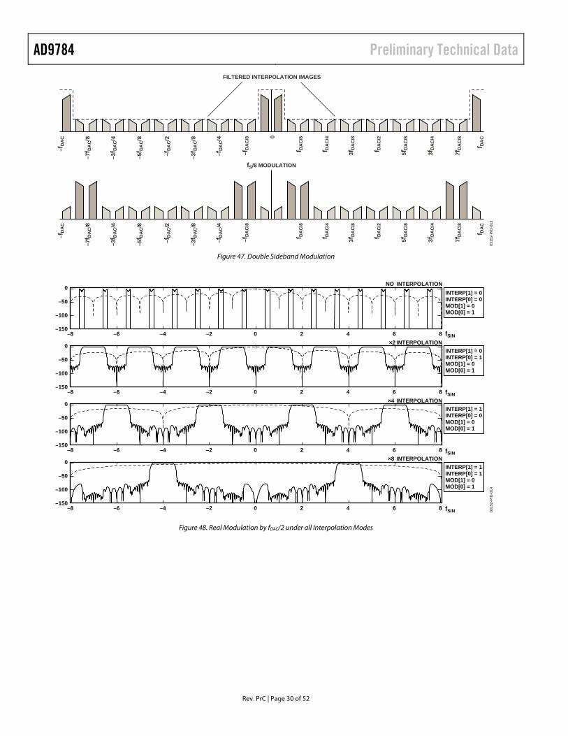
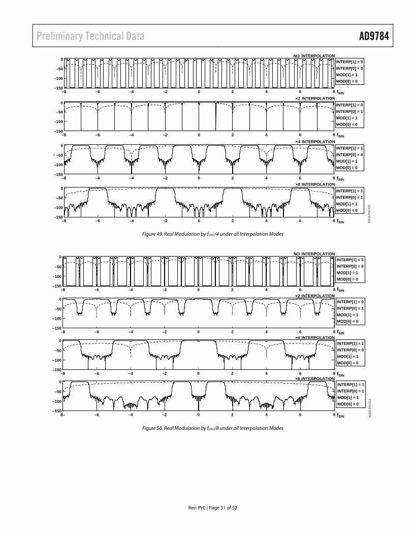
MODULATION MODES
Table 29. Single Channel Modulation MODDUAL CHANNEL MOD[1] MOD[0] Mode 0 0 0 0 I Channel, no modulation 0 0 0 1 I Channel, modulation by fDAC/2 0 0 1 0 I Channel, modulation by fDAC/4 0 0 1 1 I Channel, modulation by fDAC/8 0 1 0 0 Q Channel, no modulation 0 1 0 1 Q Channel, modulation by fDAC/2 0 1 1 0 Q Channel, modulation by fDAC/4 0 1 1 1 Q Channel, modulation by fDAC/8
Either channel of the AD9784’s interpolation filter channels can be routed to the DAC and modulated. In single channel operation the input data may be modulated by a real sinusoid; the input data and the modulating sinusoid will contain both positive and negative frequency components. A double sideband output results when modulating two real signals. At the DAC output the positive and negative frequency components will add in phase resulting in constructive signal summation.
As the modulating sinusoidal frequency becomes a larger fraction of the DAC update rate, fDAC, the more the sinc function of the DAC shapes the modulated signal bandwidth, and the closer the first image moves. As the AD9784 interpolation filter’s pass band represents a large portion of the input data’s Nyquist band, under certain modulation and interpolation modes it is possible for modulated signal bands to touch or overlap images if sufficient interpolation is not used.
Figure 48 shows the effect of real modulation under all interpolation modes. The sinc shaping at the corners of the modulated signal band and the bandwidth to the first image for those cases whose pass bands do not touch or overlap are tabulated.
Table 30. Interpolation Modulation None ×2 ×4 ×8 none fSIN 2 fSIN 4 fSIN 8 fSIN fDAC/2 fSIN 2 fSIN 4 fSIN 8 fSIN fDAC/4 Overlap Touching 2 fSIN 4 fSIN fDAC/8 Overlap Overlap Touching 6 fSIN Table 31. Interpolation Modulation None ×2 ×4 ×8 None 0 0 0 0 –2.8241 –0.6708 –0.1657 –0.0413 fDAC/2 –0.0701 –1.1932 –2.3248 –3.0590 –22.5378 –9.1824 –6.1190 –4.9337 fDAC/4 Overlap Touching –0.2921 –0.5974 –1.9096 –1.3607 fDAC/8 Overlap Overlap Touching –0.0727 –0.4614 Modulated pass band edges sinc shaping(lower/upper).
AD9784 Preliminary Technical Data
Rev. PrC | Page 30 of 52
0
–fD
AC
–7f D
AC
/8
–3f D
AC
/4
–5f D
AC
/8
– fD
AC
/2
–3f D
AC
/8
– fD
AC
/4
–fD
AC
/8
f DA
C/8
f DA
C/4
3fD
AC
/8
f DA
C/2
5fD
AC
/8
3fD
AC
/4
7fD
AC
/8
f DA
C
FILTERED INTERPOLATION IMAGES
fS/8 MODULATION
–fD
AC
–7f D
AC
/8
–3f D
AC
/4
–5f D
AC
/8
– fD
AC
/2
–3f D
AC
/8
– fD
AC
/4
–fD
AC
/8
f DA
C/8
f DA
C/4
3fD
AC
/8
f DA
C/2
5fD
AC
/8
3fD
AC
/4
7fD
AC
/8
f DA
C
0315
2-Pr
D-0
13
Figure 47. Double Sideband Modulation
–8 –6 –4 –2 0 2 4 6 8–150
–100
–50
0NO INTERPOLATION
×2 INTERPOLATIONfSIN
fSIN×4 INTERPOLATION
fSIN×8 INTERPOLATION
fSIN
INTERP[1] = 0INTERP[0] = 0MOD[1] = 0MOD[0] = 1
INTERP[1] = 0INTERP[0] = 1MOD[1] = 0MOD[0] = 1
INTERP[1] = 1INTERP[0] = 0MOD[1] = 0MOD[0] = 1
INTERP[1] = 1INTERP[0] = 1MOD[1] = 0MOD[0] = 1
–8 –6 –4 –2 0 2 4 6 8–150
–100
–50
0
–8 –6 –4 –2 0 2 4 6 8–150
–100
–50
0
–8 –6 –4 –2 0 2 4 6 8–150
–100
–50
0
0315
2-Pr
D-0
14
Figure 48. Real Modulation by fDAC/2 under all Interpolation Modes
Preliminary Technical Data AD9784
Rev. PrC | Page 31 of 52
–8 –6 –4 –2 0 2 4 6 8–150
–100
–50
0NO INTERPOLATION
×2 INTERPOLATIONfSIN
×4 INTERPOLATION
×8 INTERPOLATION
INTERP[1] = 0INTERP[0] = 0MOD[1] = 1MOD[0] = 0
–8 –6 –4 –2 0 2 4 6 8–150
–100
–50
fSIN
INTERP[1] = 0INTERP[0] = 1MOD[1] = 1MOD[0] = 0
–8 –6 –4 –2 0 2 4 6 8–150
–100
–50
fSIN
INTERP[1] = 1INTERP[0] = 0MOD[1] = 1MOD[0] = 0
–8 –6 –4 –2 0 2 4 6 8–150
–100
–50
fSIN
INTERP[1] = 1INTERP[0] = 1MOD[1] = 1MOD[0] = 0
0321
5-Pr
D-0
15
0
0
0
Figure 49. Real Modulation by fDAC/4 under all Interpolation Modes
–8 –6 –4 –2 0 2 4 6 8–150
–100
–50
0NO INTERPOLATION
×2 INTERPOLATIONfSIN
fSIN×4 INTERPOLATION
fSIN×8 INTERPOLATION
fSIN
INTERP[1] = 0INTERP[0] = 0MOD[1] = 1MOD[0] = 0
INTERP[1] = 0INTERP[0] = 1MOD[1] = 1MOD[0] = 0
INTERP[1] = 1INTERP[0] = 0MOD[1] = 1MOD[0] = 0
INTERP[1] = 1INTERP[0] = 1MOD[1] = 1MOD[0] = 0
–8 –6 –4 –2 0 2 4 6 8–150
–100
–50
0
–8 –6 –4 –2 0 2 4 6 8–150
–100
–50
0
8– –6 –4 –2 0 2 4 6 8–150
–100
–50
0
0315
2-Pr
D-0
17
Figure 50. Real Modulation by fDAC/8 under all Interpolation Modes
AD9784 Preliminary Technical Data
Rev. PrC | Page 32 of 52
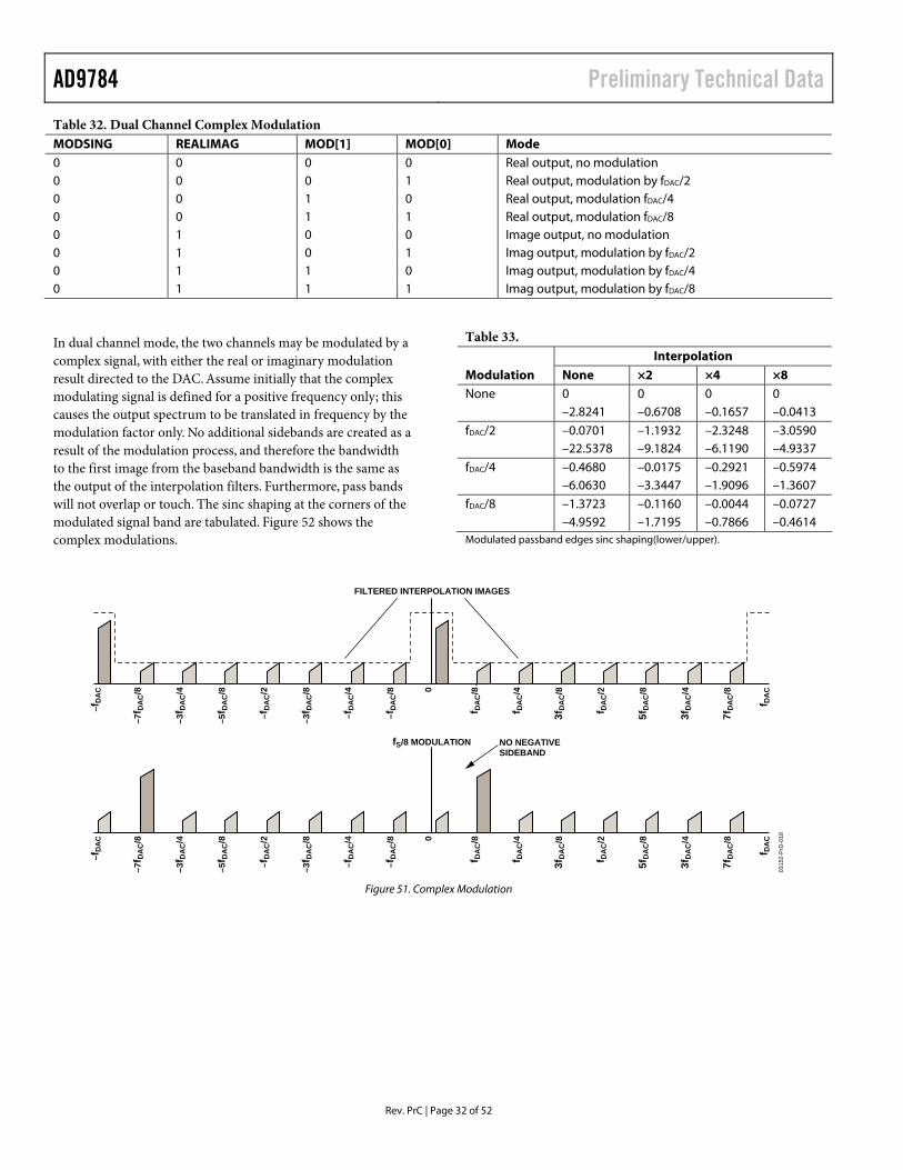
Table 32. Dual Channel Complex Modulation MODSING REALIMAG MOD[1] MOD[0] Mode 0 0 0 0 Real output, no modulation 0 0 0 1 Real output, modulation by fDAC/2 0 0 1 0 Real output, modulation fDAC/4 0 0 1 1 Real output, modulation fDAC/8 0 1 0 0 Image output, no modulation 0 1 0 1 Imag output, modulation by fDAC/2 0 1 1 0 Imag output, modulation by fDAC/4 0 1 1 1 Imag output, modulation by fDAC/8
In dual channel mode, the two channels may be modulated by a complex signal, with either the real or imaginary modulation result directed to the DAC. Assume initially that the complex modulating signal is defined for a positive frequency only; this causes the output spectrum to be translated in frequency by the modulation factor only. No additional sidebands are created as a result of the modulation process, and therefore the bandwidth to the first image from the baseband bandwidth is the same as the output of the interpolation filters. Furthermore, pass bands will not overlap or touch. The sinc shaping at the corners of the modulated signal band are tabulated. Figure 52 shows the complex modulations.
Table 33. Interpolation Modulation None ×2 ×4 ×8 None 0 0 0 0 –2.8241 –0.6708 –0.1657 –0.0413 fDAC/2 –0.0701 –1.1932 –2.3248 –3.0590 –22.5378 –9.1824 –6.1190 –4.9337 fDAC/4 –0.4680 –0.0175 –0.2921 –0.5974 –6.0630 –3.3447 –1.9096 –1.3607 fDAC/8 –1.3723 –0.1160 –0.0044 –0.0727 –4.9592 –1.7195 –0.7866 –0.4614 Modulated passband edges sinc shaping(lower/upper).
–fD
AC
–7f D
AC
/8
–3f D
AC
/4
–5f D
AC
/8
– fD
AC
/2
–3f D
AC
/8
– fD
AC
/4
– fD
AC
/8 0
f DA
C/8
f DA
C/4
3fD
AC
/8
f DA
C/2
5fD
AC
/8
3fD
AC
/4
7fD
AC
/8
f DA
C
FILTERED INTERPOLATION IMAGES
fS/8 MODULATION NO NEGATIVESIDEBAND
–fD
AC
–7f D
AC
/8
–3f D
AC
/4
–5f D
AC
/8
– fD
AC
/2
–3f D
AC
/8
– fD
AC
/4
– fD
AC
/8 0
f DA
C/8
f DA
C/4
3fD
AC
/8
f DA
C/2
5fD
AC
/8
3fD
AC
/4
7fD
AC
/8
f DA
C
0315
2-Pr
D-0
18
Figure 51. Complex Modulation
Preliminary Technical Data AD9784
Rev. PrC | Page 33 of 52
0315
2-Pr
D-0
19
–8 –6 –4 –2 0 2 4 6 8–150
–100
–50
0
0
0
×2INTERPOLATION
×4INTERPOLATION
×8INTERPOLATION
fSIN
–8 –6 –4 –2 0 2 4 6 8–150
–100
–50
fSIN
–8 –6 –4 –2 0 2 4 6 8–150
–100
–50
fSIN
INTERP[1] = 0INTERP[0] = 1MOD[1] = 0MOD[0] = 1
INTERP[1] = 1INTERP[0] = 0MOD[1] = 0MOD[0] = 1
INTERP[1] = 1INTERP[0] = 1MOD[1] = 0MOD[0] = 1
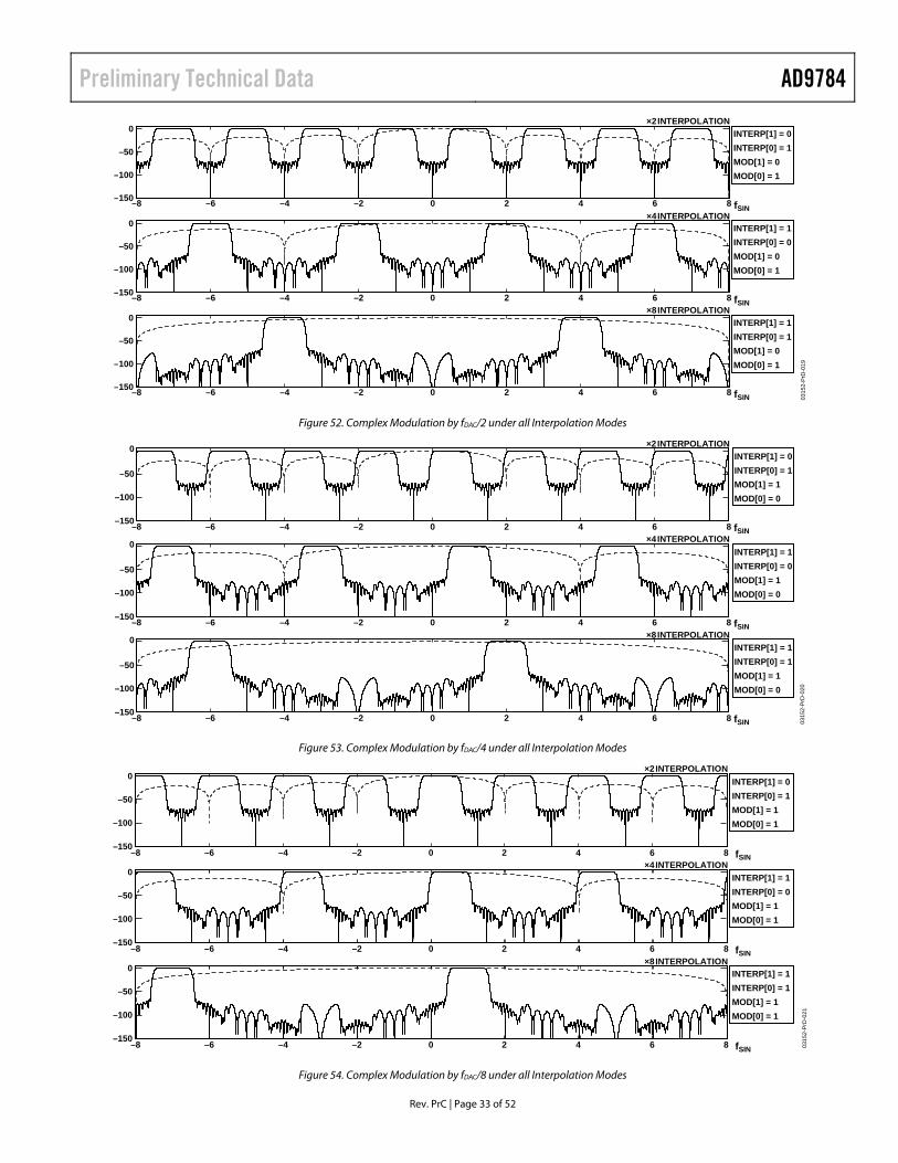
Figure 52. Complex Modulation by fDAC/2 under all Interpolation Modes
–8 –6 –4 –2 0 2 4 6 8–150
–100
–50
0 ×2INTERPOLATION
×4INTERPOLATION
×8INTERPOLATION
fSIN
INTERP[1] = 0INTERP[0] = 1MOD[1] = 1MOD[0] = 0
–8 –6 –4 –2 0 2 4 6 8–150
–100
–50
0
fSIN
INTERP[1] = 1INTERP[0] = 0MOD[1] = 1MOD[0] = 0
–8 –6 –4 –2 0 2 4 6 8–150
–100
–50
0
fSIN
INTERP[1] = 1INTERP[0] = 1MOD[1] = 1MOD[0] = 0
0315
2-Pr
D-0
20
Figure 53. Complex Modulation by fDAC/4 under all Interpolation Modes
–8 –6 –4 –2 0 2 4 6 8–150
–100
–50
0×2INTERPOLATION
×4INTERPOLATION
×8INTERPOLATION
fSIN
INTERP[1] = 0INTERP[0] = 1MOD[1] = 1MOD[0] = 1
–8 –6 –4 –2 0 2 4 6 8–150
–100
–50
0
fSIN
INTERP[1] = 1INTERP[0] = 0MOD[1] = 1MOD[0] = 1
–8 –6 –4 –2 0 2 4 6 8–150
–100
–50
0
fSIN
INTERP[1] = 1INTERP[0] = 1MOD[1] = 1MOD[0] = 1
0315
2-Pr
D-0
21
Figure 54. Complex Modulation by fDAC/8 under all Interpolation Modes
AD9784 Preliminary Technical Data
Rev. PrC | Page 34 of 52
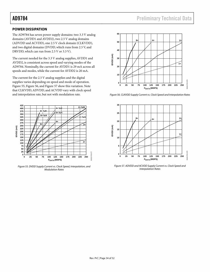
POWER DISSIPATION The AD9784 has seven power supply domains: two 3.3 V analog domains (AVDD1 and AVDD2), two 2.5 V analog domains (ADVDD and ACVDD), one 2.5 V clock domain (CLKVDD), and two digital domains (DVDD, which runs from 2.5 V, and DRVDD, which can run from 2.5 V or 3.3 V).
The current needed for the 3.3 V analog supplies, AVDD1 and AVDD2, is consistent across speed and varying modes of the AD9784. Nominally, the current for AVDD1 is 29 mA across all speeds and modes, while the current for AVDD2 is 20 mA.
The current for the 2.5 V analog supplies and the digital supplies varies depending on speed and mode of operation. Figure 55, Figure 56, and Figure 57 show this variation. Note that CLKVDD, ADVDD, and ACVDD vary with clock speed and interpolation rate, but not with modulation rate.
0315
2-Pr
D-0
77
FDATA (MSPS)2500 25 50 75 100 125 150 175 200 225
IDVD
D (m
A)
0
425
325300275250225200175
400375350
150125100
755025
1×
2×
2× fs/4
2× fs/8
4×
4× fs/4
4× fs/8
8×
8× fs/4
8× fs/8
Figure 55. DVDD Supply Current vs. Clock Speed, Interpolation, and Modulation Rates
0315
2-Pr
D-0
78
FDATA (MSPS)2500 25 50 75 100 125 150 175 200 225
IDVD
D (m
A)
0
60
50
40
30
20
10
2×
1×
4×8×
Figure 56. CLKVDD Supply Current vs. Clock Speed and Interpolation Rates
0315
2-Pr
D-0
79
FDATA (MSPS)2500 25 50 75 100 125 150 175 200 225
IDVD
D (m
A)
0
30
25
20
15
10
5
2×
1×
4×8×
Figure 57. ADVDD and ACVDD Supply Current vs. Clock Speed and Interpolation Rates
Preliminary Technical Data AD9784
Rev. PrC | Page 35 of 52
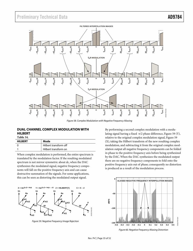
FILTERED INTERPOLATION IMAGES
fS/8 MODULATION
fS/4 MODULATION
–fD
AC
–7f D
AC
/8
–3f D
AC
/4
–5f D
AC
/8
–fD
AC
/2
–3f D
AC
/8
–fD
AC
/8 00
0
f DA
C/8
f DA
C/4
3fD
AC
/8
f DA
C/2
5fD
AC
/8
3fD
AC
/4
7fD
AC
/8
f DA
C
–fD
AC
/4
–fD
AC
–7f D
AC
/8
–3f D
AC
/4
–5f D
AC
/8
–fD
AC
/2
–3f D
AC
/8
–fD
AC
/8
f DA
C/8
f DA
C/4
3fD
AC
/8
f DA
C/2
5fD
AC
/8
3fD
AC
/4
7fD
AC
/8
f DA
C
–fD
AC
/4
– fD
AC
–7f D
AC
/8
–3f D
AC
/4
–5f D
AC
/8
–fD
AC
/2
–3f D
AC
/8
–fD
AC
/8
f DA
C/8
f DA
C/4
3fD
AC
/8
f DA
C/2
5fD
AC
/8
3fD
AC
/4
7fD
AC
/8
f DA
C
–fD
AC
/4
0315
2-Pr
D-0
22
Figure 58. Complex Modulation with Negative Frequency Aliasing
DUAL CHANNEL COMPLEX MODULATION WITH HILBERT Table 34. HILBERT Mode 0 Hilbert transform off 1 Hilbert transform on
When complex modulation is performed, the entire spectrum is translated by the modulation factor. If the resulting modulated spectrum is not mirror symmetric about dc, when the DAC synthesizes the modulated signal, negative frequency compo-nents will fall on the positive frequency axis and can cause destructive summation of the signals. For some applications, this can be seen as distorting the modulated output signal.
ReIm
f
ReIm
f
ReIm
f
ReIm
f
0000
A/2 A/2A/2A/2
A
A
A/2
A/2A/2A/2
A/2
A/2 A/2 A/2
X = Aej2π(f + fm)t Y = Aej2π(f + fm)t – π/2 Z = HILBERT(Y) C = X – Z
0315
2-Pr
D-0
23
Figure 59. Negative Frequency Image Rejection
By performing a second complex modulation with a modu-lating signal having a fixed π/2 phase difference, Figure 59 (Y), relative to the original complex modulation signal, Figure 59 (X), taking the Hilbert transform of the new resulting complex modulation, and subtracting it from the original complex mod-ulation output all negative frequency components can be folded in phase to the positive frequency axis before being synthesized by the DAC. When the DAC synthesizes the modulated output there are no negative frequency components to fold onto the positive frequency axis out of phase; consequently no distortion is produced as a result of the modulation process.
0315
2-Pr
D-0
24
0.5–0.5 –0.4 –0.3 –0.2 –0.1 0 0.1 0.2 0.3 0.4
dBFS
–150
0
–50
–100
ALIASED NEGATIVE FREQUENCY INTERPOLATION IMAGES
Figure 60. Negative Frequency Aliasing Distortion
AD9784 Preliminary Technical Data
Rev. PrC | Page 36 of 52
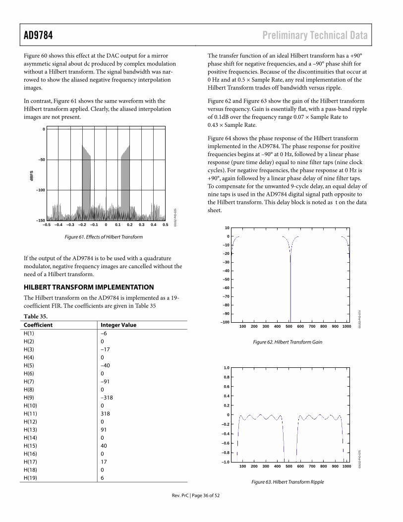
Figure 60 shows this effect at the DAC output for a mirror asymmetic signal about dc produced by complex modulation without a Hilbert transform. The signal bandwidth was nar-rowed to show the aliased negative frequency interpolation images.
In contrast, Figure 61 shows the same waveform with the Hilbert transform applied. Clearly, the aliased interpolation images are not present.
0315
2-Pr
D-0
25
0.5–0.5 –0.4 –0.3 –0.2 –0.1 0 0.1 0.2 0.3 0.4
dBFS
–150
0
–50
–100
Figure 61. Effects of Hilbert Transform
If the output of the AD9784 is to be used with a quadrature modulator, negative frequency images are cancelled without the need of a Hilbert transform.
HILBERT TRANSFORM IMPLEMENTATION The Hilbert transform on the AD9784 is implemented as a 19-coefficient FIR. The coefficients are given in Table 35
Table 35. Coefficient Integer Value H(1) –6 H(2) 0 H(3) –17 H(4) 0 H(5) –40 H(6) 0 H(7) –91 H(8) 0 H(9) –318 H(10) 0 H(11) 318 H(12) 0 H(13) 91 H(14) 0 H(15) 40 H(16) 0 H(17) 17 H(18) 0 H(19) 6
The transfer function of an ideal Hilbert transform has a +90° phase shift for negative frequencies, and a –90° phase shift for positive frequencies. Because of the discontinuities that occur at 0 Hz and at 0.5 × Sample Rate, any real implementation of the Hilbert Transform trades off bandwidth versus ripple.
Figure 62 and Figure 63 show the gain of the Hilbert transform versus frequency. Gain is essentially flat, with a pass-band ripple of 0.1dB over the frequency range 0.07 × Sample Rate to 0.43 × Sample Rate.
Figure 64 shows the phase response of the Hilbert transform implemented in the AD9784. The phase response for positive frequencies begins at –90° at 0 Hz, followed by a linear phase response (pure time delay) equal to nine filter taps (nine clock cycles). For negative frequencies, the phase response at 0 Hz is +90°, again followed by a linear phase delay of nine filter taps. To compensate for the unwanted 9-cycle delay, an equal delay of nine taps is used in the AD9784 digital signal path opposite to the Hilbert transform. This delay block is noted as t on the data sheet.
0315
2-Pr
D-0
74
1000100 200 300 400 500 600 700 800 900–100
10
–20
–60
0
–40
–30
–70
–80
–90
–10
–50
Figure 62. Hilbert Transform Gain
03
152-
PrD
-075
1000100 200 300 400 500 600 700 800 900–1.0
1.0
0.4
–0.4
0.8
0
0.2
–0.6
–0.8
0.6
–0.2
Figure 63. Hilbert Transform Ripple
Preliminary Technical Data AD9784
Rev. PrC | Page 37 of 52
0315
2-Pr
D-0
76
1200100 200 400 600 800 1000–4
4
3
–1
1
2
–2
–3
0
Figure 64. Phase Response of Hilbert Transform
Table 36. Dual Channel Complex Modulation Sideband Selection Sideband Mode 0 Lower IF sideband rejected 1 Upper IF sideband rejected
090
AD9784
AD9784
LO
I
QIm()
Re()
0315
1-Pr
D-0
03
Figure 65. AD9784 Driving Quadrature Modulator
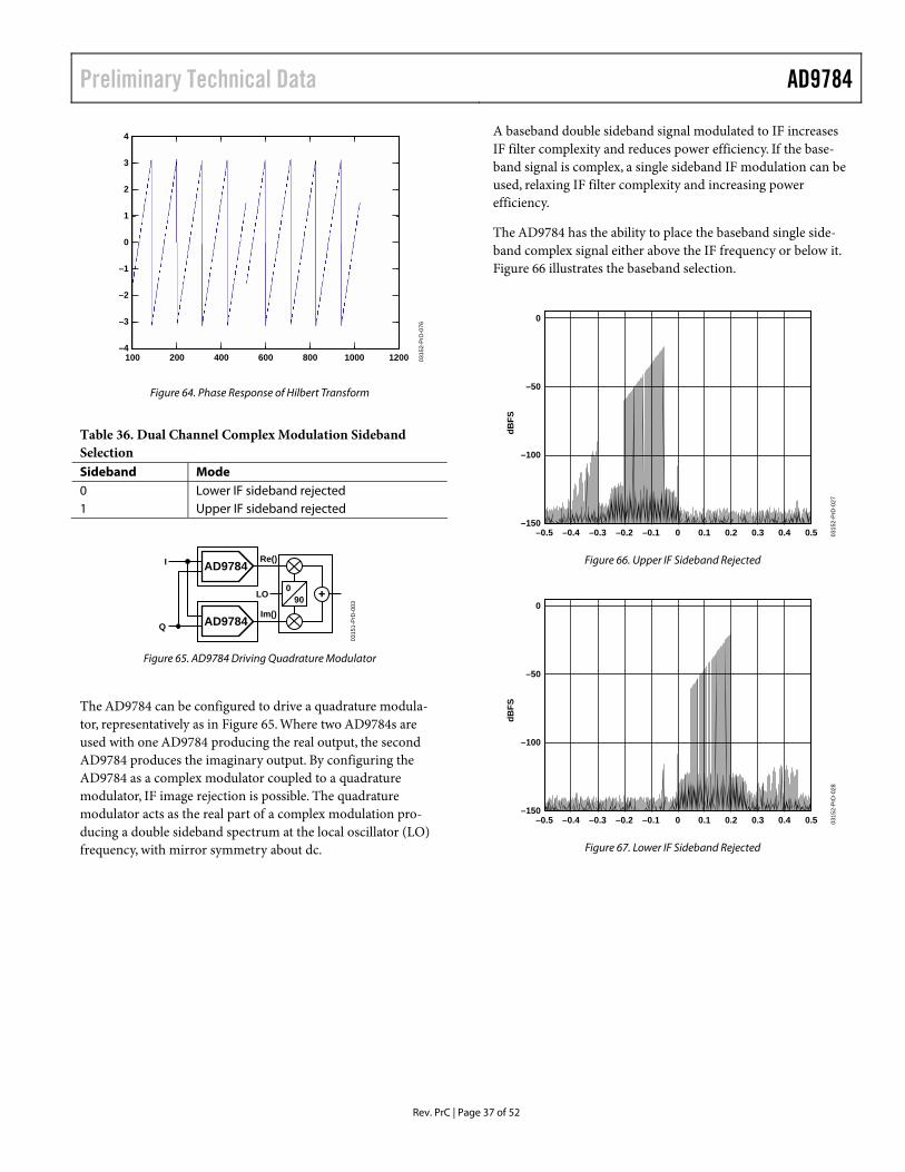
The AD9784 can be configured to drive a quadrature modula-tor, representatively as in Figure 65. Where two AD9784s are used with one AD9784 producing the real output, the second AD9784 produces the imaginary output. By configuring the AD9784 as a complex modulator coupled to a quadrature modulator, IF image rejection is possible. The quadrature modulator acts as the real part of a complex modulation pro-ducing a double sideband spectrum at the local oscillator (LO) frequency, with mirror symmetry about dc.
A baseband double sideband signal modulated to IF increases IF filter complexity and reduces power efficiency. If the base-band signal is complex, a single sideband IF modulation can be used, relaxing IF filter complexity and increasing power efficiency.
The AD9784 has the ability to place the baseband single side-band complex signal either above the IF frequency or below it. Figure 66 illustrates the baseband selection.
0315
2-Pr
D-0
27
0.5–0.5 –0.4 –0.3 –0.2 –0.1 0 0.1 0.2 0.3 0.4
dBFS
–150
0
–50
–100
Figure 66. Upper IF Sideband Rejected
0315
2-Pr
D-0
28
0.5–0.5 –0.4 –0.3 –0.2 –0.1 0 0.1 0.2 0.3 0.4
dBFS
–150
0
–50
–100
Figure 67. Lower IF Sideband Rejected
AD9784 Preliminary Technical Data
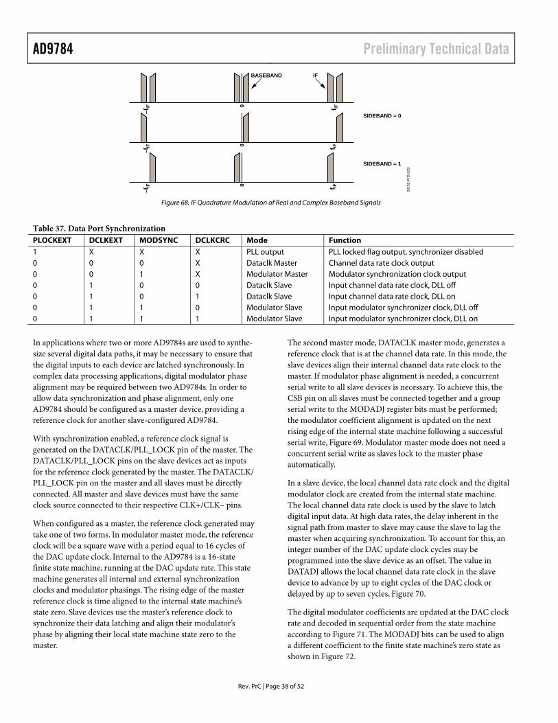
Rev. PrC | Page 38 of 52
00
f IF–fIF
–fIF f IF
0
–fIF f IF
BASEBAND IF
SIDEBAND = 0
SIDEBAND = 1
0315
2-Pr
D-0
29
Figure 68. IF Quadrature Modulation of Real and Complex Baseband Signals
Table 37. Data Port Synchronization PLOCKEXT DCLKEXT MODSYNC DCLKCRC Mode Function 1 X X X PLL output PLL locked flag output, synchronizer disabled 0 0 0 X Dataclk Master Channel data rate clock output 0 0 1 X Modulator Master Modulator synchronization clock output 0 1 0 0 Dataclk Slave Input channel data rate clock, DLL off 0 1 0 1 Dataclk Slave Input channel data rate clock, DLL on 0 1 1 0 Modulator Slave Input modulator synchronizer clock, DLL off 0 1 1 1 Modulator Slave Input modulator synchronizer clock, DLL on
In applications where two or more AD9784s are used to synthe-size several digital data paths, it may be necessary to ensure that the digital inputs to each device are latched synchronously. In complex data processing applications, digital modulator phase alignment may be required between two AD9784s. In order to allow data synchronization and phase alignment, only one AD9784 should be configured as a master device, providing a reference clock for another slave-configured AD9784.
With synchronization enabled, a reference clock signal is generated on the DATACLK/PLL_LOCK pin of the master. The DATACLK/PLL_LOCK pins on the slave devices act as inputs for the reference clock generated by the master. The DATACLK/ PLL_LOCK pin on the master and all slaves must be directly connected. All master and slave devices must have the same clock source connected to their respective CLK+/CLK– pins.
When configured as a master, the reference clock generated may take one of two forms. In modulator master mode, the reference clock will be a square wave with a period equal to 16 cycles of the DAC update clock. Internal to the AD9784 is a 16-state finite state machine, running at the DAC update rate. This state machine generates all internal and external synchronization clocks and modulator phasings. The rising edge of the master reference clock is time aligned to the internal state machine’s state zero. Slave devices use the master’s reference clock to synchronize their data latching and align their modulator’s phase by aligning their local state machine state zero to the master.
The second master mode, DATACLK master mode, generates a reference clock that is at the channel data rate. In this mode, the slave devices align their internal channel data rate clock to the master. If modulator phase alignment is needed, a concurrent serial write to all slave devices is necessary. To achieve this, the CSB pin on all slaves must be connected together and a group serial write to the MODADJ register bits must be performed; the modulator coefficient alignment is updated on the next rising edge of the internal state machine following a successful serial write, Figure 69. Modulator master mode does not need a concurrent serial write as slaves lock to the master phase automatically.
In a slave device, the local channel data rate clock and the digital modulator clock are created from the internal state machine. The local channel data rate clock is used by the slave to latch digital input data. At high data rates, the delay inherent in the signal path from master to slave may cause the slave to lag the master when acquiring synchronization. To account for this, an integer number of the DAC update clock cycles may be programmed into the slave device as an offset. The value in DATADJ allows the local channel data rate clock in the slave device to advance by up to eight cycles of the DAC clock or delayed by up to seven cycles, Figure 70.
The digital modulator coefficients are updated at the DAC clock rate and decoded in sequential order from the state machine according to Figure 71. The MODADJ bits can be used to align a different coefficient to the finite state machine’s zero state as shown in Figure 72.
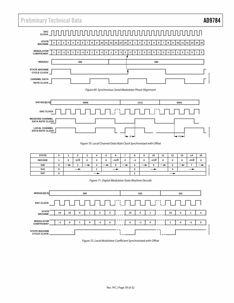
Preliminary Technical Data AD9784
Rev. PrC | Page 39 of 52
DACCLOCK
STATEMACHINE
STATE MACHINE
CHANNEL DATA
CYCLE CLOCK
RATE CLOCK
MODULATORCOEFFICIENT
MODADJ 000 000
1 0 –1 0 1 0 –1 0 1 0 –1 0 1 0 –1 0 –1 0 1 0 –1 0 1 0 –1 0 1 0 –1 0 1 0
0 1 2 3 4 5 6 7 8 9 10 11 12 13 14 15 0 1 2 3 4 5 6 7 8 9 10 11 12 13 14 15
0315
2-Pr
D-0
30
Figure 69. Synchronous Serial Modulator Phase Alignment
DATADJ[3:0]
DAC CLOCK
RECEIVED CHANNELDATA RATE CLOCK
LOCAL CHANNELDATA RATE CLOCK
0000 00011111
0315
2-Pr
D-0
31
–1 +1
Figure 70. Local Channel Data Rate Clock Synchronized with Offset
1
fs/2
STATE 2 3 4 5 6 7 8 9 10 11 12 13 4 1510
0 1
0315
2-Pr
D-0
32
DECODE 0 0 0 0 0 –1 0 0 0 0 01 1/ 2 –1/ 2 –1/ 2 –1/ 2
fs/4 1 2 30
fs/8 1 2 3 4 5 6 70
Figure 71. Digital Modulator State Machine Decode
MODADJ[2:0]
DAC CLOCK
STATE MACHINECYCLE CLOCK
000 101010
STATEMACHINE
MODULATORCOEFFICIENT
0315
2-Pr
D-0
33
–1 0 1 0 –1 0 0 –1 0 1 0 –1 0
14 15 0 1 2 3 15 0 1 15 0 1 2
Figure 72. Local Modulator Coefficient Synchronized with Offset
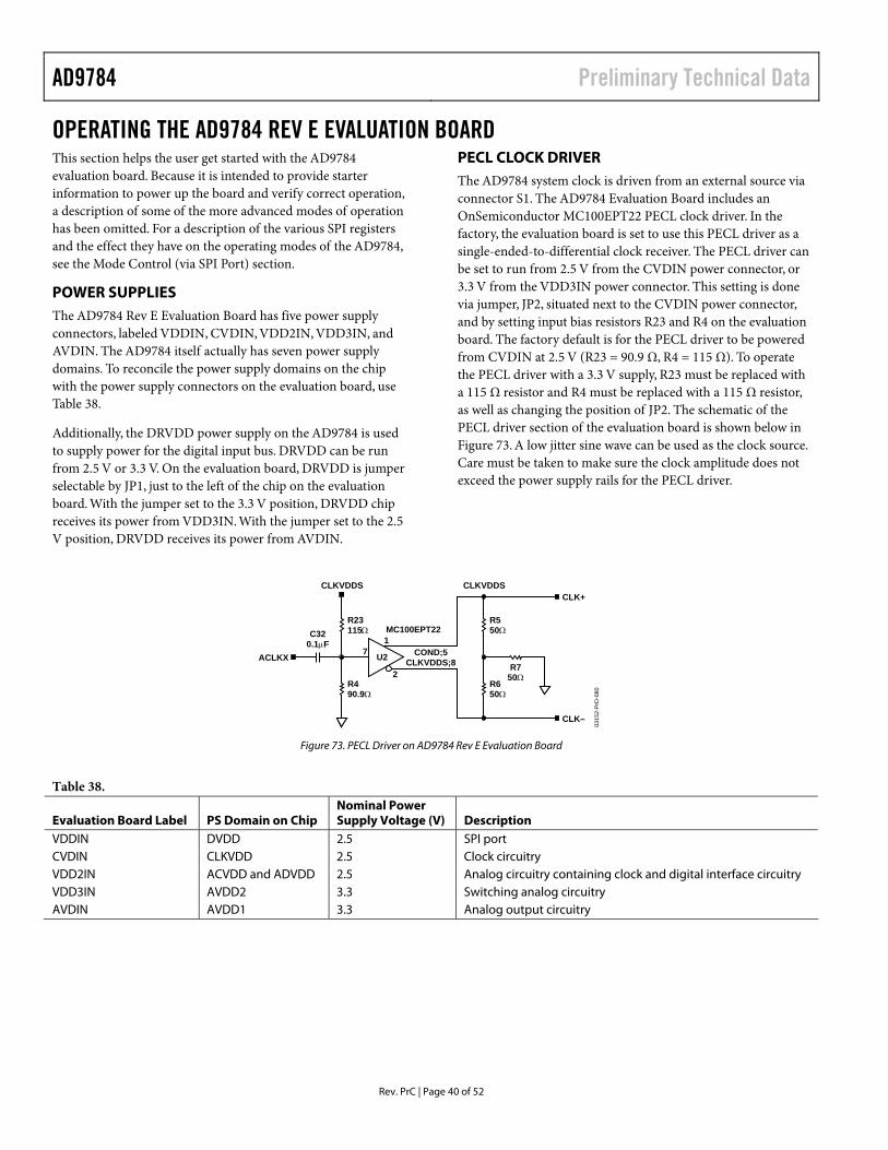
AD9784 Preliminary Technical Data
Rev. PrC | Page 40 of 52
OPERATING THE AD9784 REV E EVALUATION BOARD This section helps the user get started with the AD9784 evaluation board. Because it is intended to provide starter information to power up the board and verify correct operation, a description of some of the more advanced modes of operation has been omitted. For a description of the various SPI registers and the effect they have on the operating modes of the AD9784, see the Mode Control (via SPI Port) section.
POWER SUPPLIES The AD9784 Rev E Evaluation Board has five power supply connectors, labeled VDDIN, CVDIN, VDD2IN, VDD3IN, and AVDIN. The AD9784 itself actually has seven power supply domains. To reconcile the power supply domains on the chip with the power supply connectors on the evaluation board, use Table 38.
Additionally, the DRVDD power supply on the AD9784 is used to supply power for the digital input bus. DRVDD can be run from 2.5 V or 3.3 V. On the evaluation board, DRVDD is jumper selectable by JP1, just to the left of the chip on the evaluation board. With the jumper set to the 3.3 V position, DRVDD chip receives its power from VDD3IN. With the jumper set to the 2.5 V position, DRVDD receives its power from AVDIN.
PECL CLOCK DRIVER The AD9784 system clock is driven from an external source via connector S1. The AD9784 Evaluation Board includes an OnSemiconductor MC100EPT22 PECL clock driver. In the factory, the evaluation board is set to use this PECL driver as a single-ended-to-differential clock receiver. The PECL driver can be set to run from 2.5 V from the CVDIN power connector, or 3.3 V from the VDD3IN power connector. This setting is done via jumper, JP2, situated next to the CVDIN power connector, and by setting input bias resistors R23 and R4 on the evaluation board. The factory default is for the PECL driver to be powered from CVDIN at 2.5 V (R23 = 90.9 Ω, R4 = 115 Ω). To operate the PECL driver with a 3.3 V supply, R23 must be replaced with a 115 Ω resistor and R4 must be replaced with a 115 Ω resistor, as well as changing the position of JP2. The schematic of the PECL driver section of the evaluation board is shown below in Figure 73. A low jitter sine wave can be used as the clock source. Care must be taken to make sure the clock amplitude does not exceed the power supply rails for the PECL driver.
0315
2-Pr
D-0
80
U271
2
COND;5CLKVDDS;8
C320.1µF
R23115Ω
R490.9Ω
ACLKX
CLKVDDS
R550Ω
R750Ω
R650Ω
CLKVDDS
MC100EPT22
CLK+
CLK–
Figure 73. PECL Driver on AD9784 Rev E Evaluation Board
Table 38.
Evaluation Board Label PS Domain on Chip Nominal Power Supply Voltage (V) Description
VDDIN DVDD 2.5 SPI port CVDIN CLKVDD 2.5 Clock circuitry VDD2IN ACVDD and ADVDD 2.5 Analog circuitry containing clock and digital interface circuitry VDD3IN AVDD2 3.3 Switching analog circuitry AVDIN AVDD1 3.3 Analog output circuitry
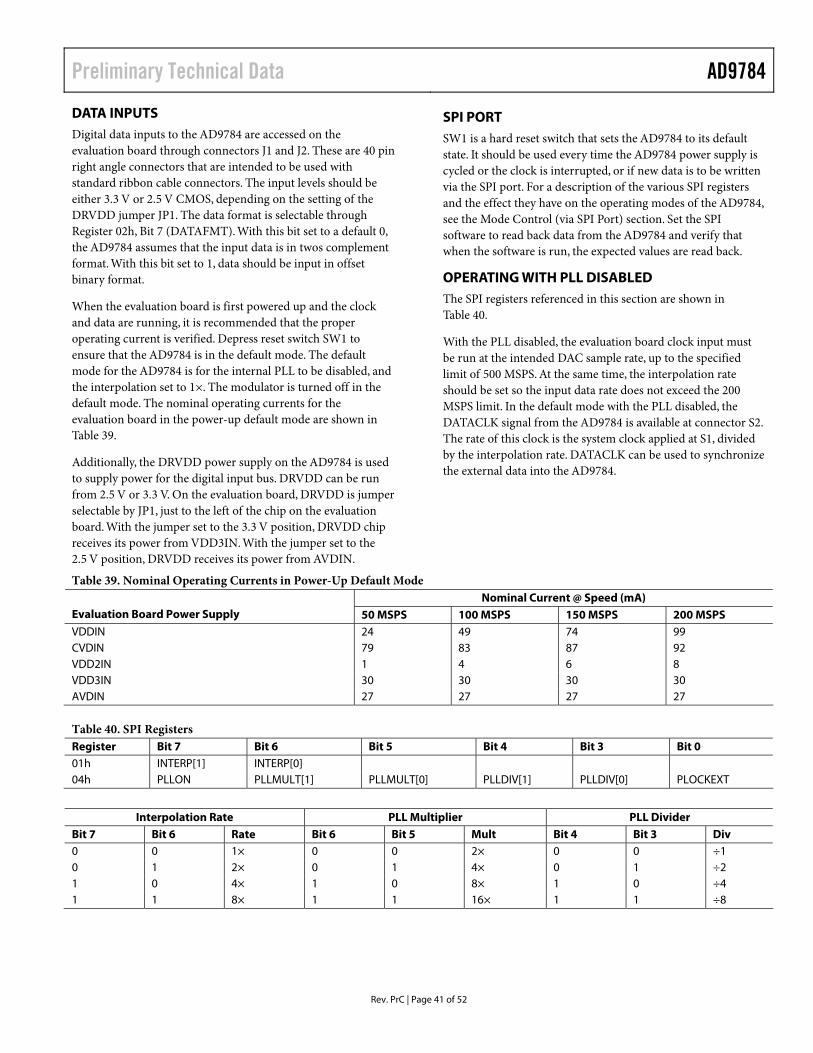
Preliminary Technical Data AD9784
Rev. PrC | Page 41 of 52
DATA INPUTS Digital data inputs to the AD9784 are accessed on the evaluation board through connectors J1 and J2. These are 40 pin right angle connectors that are intended to be used with standard ribbon cable connectors. The input levels should be either 3.3 V or 2.5 V CMOS, depending on the setting of the DRVDD jumper JP1. The data format is selectable through Register 02h, Bit 7 (DATAFMT). With this bit set to a default 0, the AD9784 assumes that the input data is in twos complement format. With this bit set to 1, data should be input in offset binary format.
When the evaluation board is first powered up and the clock and data are running, it is recommended that the proper operating current is verified. Depress reset switch SW1 to ensure that the AD9784 is in the default mode. The default mode for the AD9784 is for the internal PLL to be disabled, and the interpolation set to 1×. The modulator is turned off in the default mode. The nominal operating currents for the evaluation board in the power-up default mode are shown in Table 39.
Additionally, the DRVDD power supply on the AD9784 is used to supply power for the digital input bus. DRVDD can be run from 2.5 V or 3.3 V. On the evaluation board, DRVDD is jumper selectable by JP1, just to the left of the chip on the evaluation board. With the jumper set to the 3.3 V position, DRVDD chip receives its power from VDD3IN. With the jumper set to the 2.5 V position, DRVDD receives its power from AVDIN.
SPI PORT SW1 is a hard reset switch that sets the AD9784 to its default state. It should be used every time the AD9784 power supply is cycled or the clock is interrupted, or if new data is to be written via the SPI port. For a description of the various SPI registers and the effect they have on the operating modes of the AD9784, see the Mode Control (via SPI Port) section. Set the SPI software to read back data from the AD9784 and verify that when the software is run, the expected values are read back.
OPERATING WITH PLL DISABLED The SPI registers referenced in this section are shown in Table 40.
With the PLL disabled, the evaluation board clock input must be run at the intended DAC sample rate, up to the specified limit of 500 MSPS. At the same time, the interpolation rate should be set so the input data rate does not exceed the 200 MSPS limit. In the default mode with the PLL disabled, the DATACLK signal from the AD9784 is available at connector S2. The rate of this clock is the system clock applied at S1, divided by the interpolation rate. DATACLK can be used to synchronize the external data into the AD9784.
Table 39. Nominal Operating Currents in Power-Up Default Mode Nominal Current @ Speed (mA)
Evaluation Board Power Supply 50 MSPS 100 MSPS 150 MSPS 200 MSPS VDDIN 24 49 74 99 CVDIN 79 83 87 92 VDD2IN 1 4 6 8 VDD3IN 30 30 30 30 AVDIN 27 27 27 27 Table 40. SPI Registers Register Bit 7 Bit 6 Bit 5 Bit 4 Bit 3 Bit 0 01h INTERP[1] INTERP[0] 04h PLLON PLLMULT[1] PLLMULT[0] PLLDIV[1] PLLDIV[0] PLOCKEXT
Interpolation Rate PLL Multiplier PLL Divider Bit 7 Bit 6 Rate Bit 6 Bit 5 Mult Bit 4 Bit 3 Div 0 0 1× 0 0 2× 0 0 ÷1 0 1 2× 0 1 4× 0 1 ÷2 1 0 4× 1 0 8× 1 0 ÷4 1 1 8× 1 1 16× 1 1 ÷8
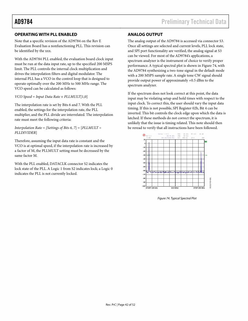
AD9784 Preliminary Technical Data
Rev. PrC | Page 42 of 52
OPERATING WITH PLL ENABLED Note that a specific revision of the AD9784 on the Rev E Evaluation Board has a nonfunctioning PLL. This revision can be identified by the xxx.
With the AD9784 PLL enabled, the evaluation board clock input must be run at the data input rate, up to the specified 200 MSPS limit. The PLL controls the internal clock multiplication and drives the interpolation filters and digital modulator. The internal PLL has a VCO in the control loop that is designed to operate optimally over the 200 MHz to 500 MHz range. The VCO speed can be calculated as follows:
VCO Speed = Input Data Rate × PLLMULT[1,0]
The interpolation rate is set by Bits 6 and 7. With the PLL enabled, the settings for the interpolation rate, the PLL multiplier, and the PLL divide are interrelated. The interpolation rate must meet the following criteria:
Interpolation Rate = [Settings of Bits 6, 7] = [PLLMULT ÷ PLLDIVIDER]
Therefore, assuming the input data rate is constant and the VCO is at optimal speed, if the interpolation rate is increased by a factor of M, the PLLMULT setting must be decreased by the same factor M.
With the PLL enabled, DATACLK connector S2 indicates the lock state of the PLL. A Logic 1 from S2 indicates lock; a Logic 0 indicates the PLL is not currently locked.
ANALOG OUTPUT The analog output of the AD9784 is accessed via connector S3. Once all settings are selected and current levels, PLL lock state, and SPI port functionality are verified, the analog signal at S3 can be viewed. For most of the AD9784’s applications, a spectrum analyzer is the instrument of choice to verify proper performance. A typical spectral plot is shown in Figure 74, with the AD9784 synthesizing a two-tone signal in the default mode with a 200 MSPS sample rate. A single tone CW signal should provide output power of approximately +0.5 dBm to the spectrum analyzer.
If the spectrum does not look correct at this point, the data input may be violating setup and hold times with respect to the input clock. To correct this, the user should vary the input data timing. If this is not possible, SPI Register 02h, Bit 4 can be inverted. This bit controls the clock edge upon which the data is latched. If these methods do not correct the spectrum, it is unlikely that the issue is timing related. This note should then be reread to verify that all instructions have been followed.
0315
2-Pr
D-0
81
10
0
–10
–20
–30
–40
–50
–60
–60
–70
–80
–90
–100START 100 kHz STOP 200 MHz19.9 MHz/
Figure 74. Typical Spectral Plot
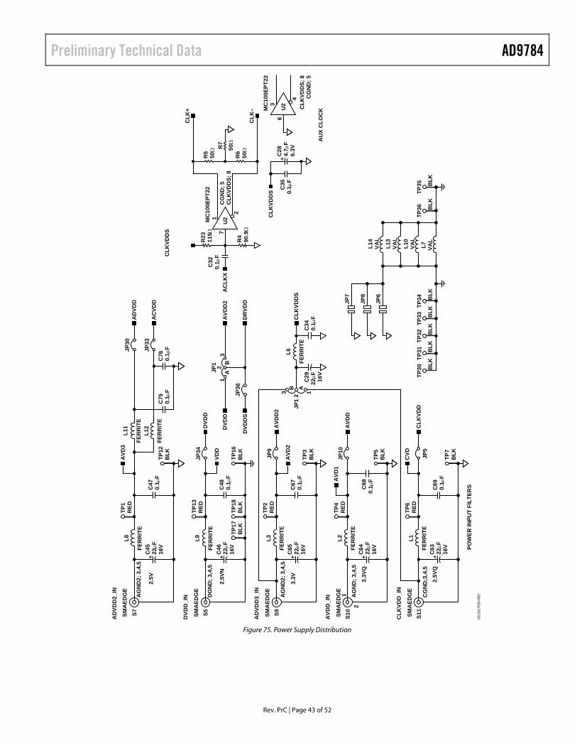
Preliminary Technical Data AD9784
Rev. PrC | Page 43 of 52
S11
CG
ND
;3,4
,5
S9A
GN
D2;
3,4
,5
S7A
GN
D2;
3,4
,5
S5D
GN
D; 3
,4,5
2
1
R7
50Ω
R5
50Ω
R6
50Ω
JP8
JP6
AVD
D_I
N
AD
VDD
2_IN
DVD
D_I
N
TP18
BLK
TP30
TP31
TP32
TP33
TP34
BLK
BLK
BLK
BLK
BLK
BLK
BLK
TP36
C28
4.7µ
F6.
3V
C75
0.1µ
F
JP33
21
CG
ND
; 5C
LKVD
DS;
82
17
CLK
VDD
S
C35
0.1µ
F
JP30
C47
0.1µ
F
AD
VDD
AC
VDD
C76
0.1µ
F
C46
22µF
16V
C45
22µF
16V
C64
22µF
16V
C68
0.1µ
F
C63
22µF
16V
CLK
VDD
S; 8
CG
ND
; 5
L9
FER
RIT
E
TP13
RED
L8
FER
RIT
E
L11
FER
RIT
EL1
2
FER
RIT
E
TP1
RED
TP12
BLK
TP2
RED
TP3
BLK
L1
FER
RIT
E
TP6
RED
TP5
BLK
C69
0.1µ
F
TP16
BLK
C48
0.1µ
F
AVD
3
L2
FER
RIT
E
TP4
RED
AVD
1
AVD
D
L3
FER
RIT
EC
6522
µF16
V
AC
LKX
L6
FER
RIT
E
CLK
VDD
S
C34
0.1µ
FCLK
VDD
S
JP10
CVD
CLK
VDD
JP5
JP36
TP7
BLK
AD
VDD
3_IN
C67
0.1µ
FC
2922
µF 16V
R23
115Ω
TP35
JP34
DVD
D
VDD
AVD
2
JP9
AVD
D2
L13
VAL
L10
VAL
L7 VAL
L14
VAL
JP7
CLK
VDD
_IN
TP17
BLK
CLK
+
CLK
–D
VDD
S
DVD
DA
VDD
2
DR
VDD
SMA
EDG
E
SMA
EDG
E
SMA
EDG
E
SMA
EDG
E
SMA
EDG
E
AG
ND
; 3,4
,5
MC
100E
PT22
S10
+ + + + +
JP1
AB
3
2 1
JP1
AB3
R4
90.9Ω
C32
0.1µ
FU
2
+
4
36
MC
100E
PT22
U2
AU
X C
LOC
K
POW
ER IN
PUT
FILT
ERS
2.5V
Q
3.3V
Q
3.3V
2.5V
N
2.5V
0315
2-Pr
D-0
82
Figure 75. Power Supply Distribution
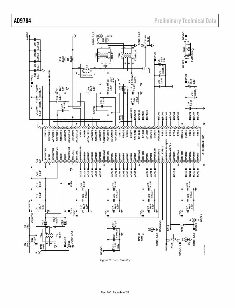
AD9784 Preliminary Technical Data
Rev. PrC | Page 44 of 52
0315
2-Pr
D-0
83
SPC
SB
BD
04
SPC
LKSP
SDI
SPSD
O
C6
10µF
6.3V
C22
0.00
1µF
C37
0.1µ
F
BD
08B
D07
DVD
DB
D06
BD
05
BD
03B
D02
BD
01B
D00RES
ET
TP11
WH
TTP
10W
HT
CLK
+C
LK–
CLK
CO
M1
CLK
CO
M2
CLK
VDD
1
CLK
VDD
2
DC
LK-P
LLL
DC
OM
1
DC
OM
2
DC
OM
3
DC
OM
4
DR
VDD
1
DVD
D1
DVD
D2
DVD
D3
DVD
D4
LPF
P1B
0LSB
P1B
1
P1B
10P1
B11
P1B
12P1
B13
P1B
14P1
B15
MSB
P1B
2
P1B
3P1
B4
P1B
5P1
B6
P1B
7P1
B8
P1B
9
P2B
10P2
B11
P2B
12
P2B
13P2
B14
-OPC
LKP2
B15
MSB
-IQSE
L
P2B
9
AC
CO
M2P
2
AC
CO
MP1
AC
OM
1P11
AC
OM
2P12
AC
OM
1P21
AC
OM
2P1
AC
OM
2P2
AC
VDD
P1
AC
VDD
P2A
DC
OM
P2
AD
VDD
P1
AD
VDD
P2
AVD
D1P
1
AVD
D1P
2
AVD
D2P
1
AVD
D2P
2
DC
OM
5
DC
OM
6
DN
C1
DVD
D5
DVD
D6
FSA
DJ
IOU
TAIO
UTB
P2B
0LSB
P2B
1P2
B2
P2B
3P2
B4
P2B
5
P2B
6P2
B7
P2B
8
REF
IOR
ESET
SP-C
LKSP
-SD
ISP
-SD
O
SPI_
CSB
DN
C2
U1
AD
9786
BTS
P
1 2 3 4 5 6 7 8 9 10 11 12 13 14 15 16 17 18 19 20 21 22 23 24 25 26 27 28 29 30 31 32 33 34 35 36 37 38 39 40
80 79 78 77 76 75 74 73 72 71 70 69 68 67 66 65 64 63 62 61 60 59 58 57 56 55 54 53 52 51 50 49 48 47 46 45 44 43 42 41
TP8
WH
T +
C5
10µF
6.3V
C21
0.00
1µF
C38
0.1µ
F
DVD
D+
SW1
4 3
RES
ET2 1
DR
VDD
FLO
AT;
5
C55
0.00
1µF
C20
0.00
1µF
C49
0.1µ
F
AVD
DC
180.
001µ
FC
40.
1µF
AVD
D2
C62
0.1µ
FC
610.
001µ
F
C16
0.1µ
FC
3010
V10
µF
+R
82.
000k
Ω0.
01%
C19
0.1µ
F
C14
0.1µ
FC
210
µF6.
3V
C17
0.1µ
F
C15
0.1µ
FC
310
µF6.
3V
+
+
C66
10µF
6.3V
+
AC
VDD
ADTL1-12
P S4
6
31
AD
VDD
R10
49.9Ω
R9
49.9Ω
T3
PS
1
4 623
NC
= 5 P
S6
3 154
NC
= 5
T2A
T2B
TC1-
1T
TTW
B-1
-B
R42
49.9Ω
OU
T1S3
S3TP
29B
LK
C12
0.1µ
FC
110
µF6.
3V
C11
0.1µ
FC
420.
1µF
C49
1pF
+
C26
0.00
1µF
C10
10µF
6.3V
C40
0.1µ
F+
BD
09B
D10
BD
11B
D12
BD
13
AD
00A
D01
AD
02
AD
03A
D04
AD
05A
D06
AD
07A
D08
AD
09
AD
10A
D11
AD
12A
D13
AD
14A
D15
DVD
D
C25
0.00
1µF
C9
10µF
6.3V
C41
0.1µ
F+
DVD
D
CLK
VDD
CLK
VDD C
LK–
CLK
+
R1
50Ω
4
1 2 356
T2A
T1T1
-1T
S1 CG
ND
; 3,4
,5
AC
LKX
TP15
WH
TR2
10kΩ
C13
0.1µ
F
R3
10kΩ
C54
0.00
1µF
C33
0.1µ
FC
3110
µF6.
3V
+
DR
VDD
C24
0.00
1µF
C8
10µF
6.3V
C39
0.1µ
F+
DVD
D
C23
0.00
1µF
C7
10µF
6.3V
C36
0.1µ
F+
DVD
D
TP14
WH
T
S2
S4
S6
BD
15
OPC
LK_3
IQ
DA
TAC
LK OPC
LK
OPC
LK
BD
14
JP27
JP28
A B
JP23
JP22
3 2 1
DG
ND
; 3,4
,5
DG
ND
; 3,4
,5
AG
ND
; 3,4
,5
AG
ND
; 3,4
,5
Figure 76. Local Circuitry
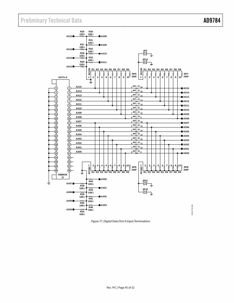
Preliminary Technical Data AD9784
Rev. PrC | Page 45 of 52
0315
2-Pr
D-0
84R43
100Ω
R44100Ω
R41100Ω
R46100Ω
R39100Ω
R38100Ω
R40100Ω
R34100Ω
R31100Ω
R30100Ω
R32100Ω
R33100Ω
R27100Ω
R26100Ω
R28100Ω
R29100Ω
1
3
5
7
9
11
13
15
17
19
21
23
25
27
29
31
33
35
37
39
2
4
6
8
10
12
14
16
18
20
22
24
26
28
30
32
34
36
38
40
DATA-A
RIBBONJ1
AX07
AX06
AX05
AX04
AX15
AX14
AX13
AX12
AX00
AX01
AX02
AX03
AX08
AX09
AX10
AX11
JP21
JP19
21 3 4 5 6 7 8 9 10
R1 R2 R3 R4 R5 R6 R7 R8 R9
21 3 4 5 6 7 8 9 10
R1 R2 R3 R4 R5 R6 R7 R8 R9RC
OM
RC
OM RP8
DNPRP6DNP
21 3 4 5 6 7 8 9 1021 3 4 5 6 7 8 9 10
R1 R2 R3 R4 R5 R6 R7 R8 R9R1 R2 R3 R4 R5 R6 R7 R8 R9
RC
OM
RC
OM
RP7DNP
RP5DNP
AD15
AD14
AD13
AD12
AD11
AD10
AD09
AD08
AD07
AD06
AD05
AD04
AD03
AD02
AD01
AD00
AX15
AX14
AX13
AX12
AX11
AX10
AX09
AX08
AX07
AX06
AX05
AX04
AX03
AX02
AX01
AX00
1 16
2 15
3 14
4 13
5 12
6 11
7 10
8 9
1 16
2 15
3 14
4 13
5 12
6 11
7 10
8 9
RP1 22
RP1 22
RP1 22
RP1 22
RP1 22
RP1 22
RP1 22
RP1 22
RP2 22
RP2 22
RP2 22
RP2 22
RP2 22
RP2 22
RP2 22
RP2 22
JP3
JP12
Figure 77. Digital Data Port A Input Terminations
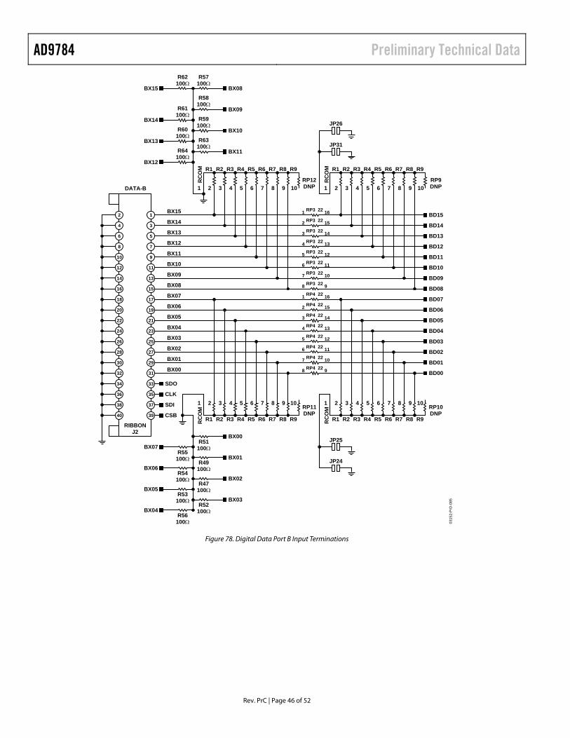
AD9784 Preliminary Technical Data
Rev. PrC | Page 46 of 52
0315
2-Pr
D-0
85
R49100Ω
R51100Ω
R47100Ω
R52100Ω
R54100Ω
R55100Ω
R53100Ω
R56100Ω
R58100Ω
R57100Ω
R59100Ω
R63100Ω
R61100Ω
R62100Ω
R60100Ω
R64100Ω
1
3
5
7
9
11
13
15
17
19
21
23
25
27
29
31
33
35
37
39
2
4
6
8
10
12
14
16
18
20
22
24
26
28
30
32
34
36
38
40
DATA-B
RIBBONJ2
BX07
BX06
BX05
BX04
BX15
BX14
BX13
BX12
BX00
BX01
BX02
BX03
BX08
BX09
BX10
BX11
JP25
JP24
21 3 4 5 6 7 8 9 10
R1 R2 R3 R4 R5 R6 R7 R8 R9
21 3 4 5 6 7 8 9 10
R1 R2 R3 R4 R5 R6 R7 R8 R9RC
OM
RC
OM RP10
DNPRP11DNP
21 3 4 5 6 7 8 9 1021 3 4 5 6 7 8 9 10
R1 R2 R3 R4 R5 R6 R7 R8 R9R1 R2 R3 R4 R5 R6 R7 R8 R9
RC
OM
RC
OM
RP9DNP
RP12DNP
BD15
BD14
BD13
BD12
BD11
BD10
BD09
BD08
BD07
BD06
BD05
BD04
BD03
BD02
BD01
BD00
BX15
BX14
BX13
BX12
BX11
BX10
BX09
BX08
BX07
BX06
BX05
BX04
BX03
BX02
BX01
BX00
SDO
CLK
SDI
CSB
1 16
2 15
3 14
4 13
5 12
6 11
7 10
8 9
1 16
2 15
3 14
4 13
5 12
6 11
7 10
8 9
RP3 22
RP3 22
RP3 22
RP3 22
RP3 22
RP3 22
RP3 22
RP3 22
RP4 22
RP4 22
RP4 22
RP4 22
RP4 22
RP4 22
RP4 22
RP4 22
JP26
JP31
Figure 78. Digital Data Port B Input Terminations
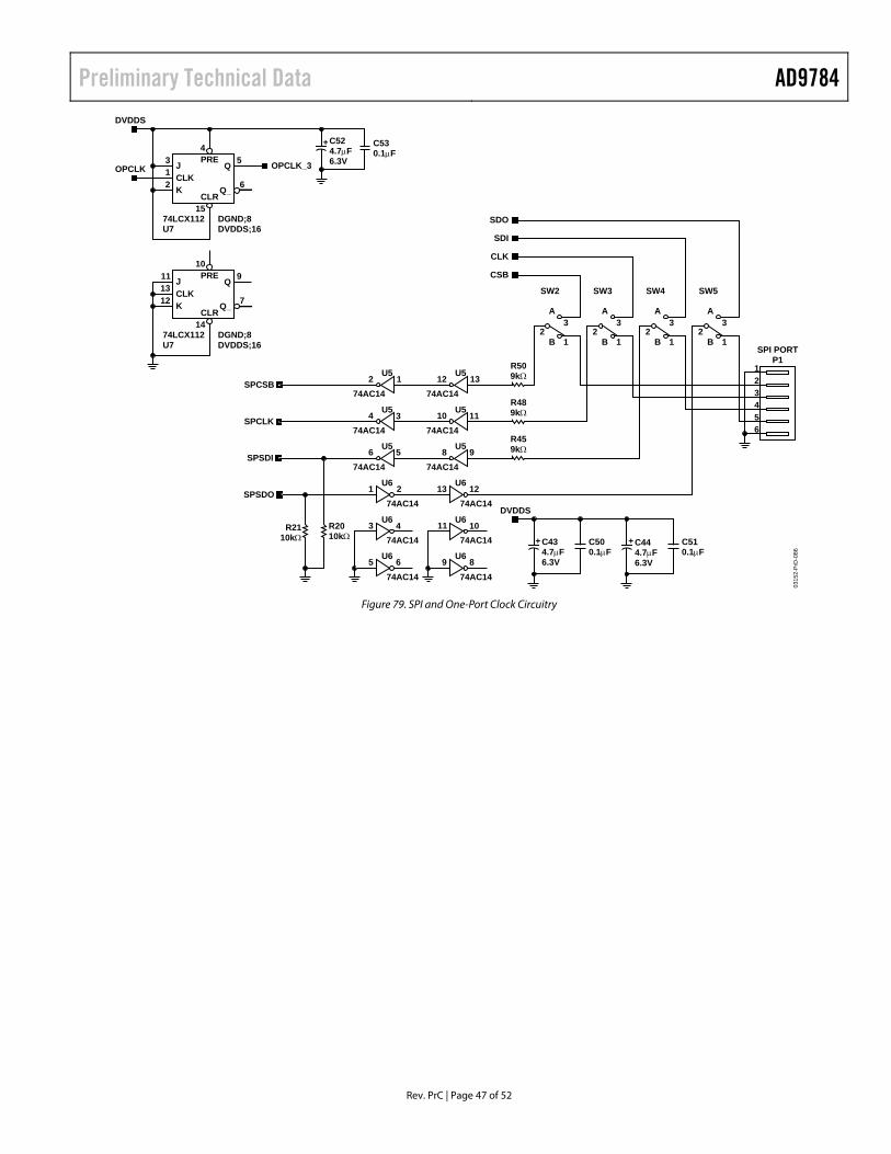
Preliminary Technical Data AD9784
Rev. PrC | Page 47 of 52
0315
2-Pr
D-0
86
DVDDS
OPCLK
DGND;8DVDDS;16
12
3
6
5
15
4 C530.1µF
C524.7µF6.3V
C444.7µF6.3V
C510.1µF
C434.7µF6.3V
C500.1µF
R509kΩ
R489kΩ
R459kΩ
OPCLK_3
SPCSB
SPCLK
R2010kΩ
SPSDI
R2110kΩ
SPSDO
U5
12 13
11
9
10
DVDDS
8
3
54
21
6
SW5
21
3
SDO
SDI
CLK
CSB
PRE
CLR
Q
Q_
J
KCLK
74LCX112U7
74AC14
74AC14
74AC14
A
BSPI PORT
P1
SW4
21
3A
B
SW3
21
3A
B
SW2
21
3A
B
U5
U5
U5
2 1
3
5
4
6
74AC14
74AC14
74AC14
U5
U5
+ +U6
13 12
10
8
11
9
74AC14
74AC14
74AC14
U6
U6
U6
1 2
4
6
3
5
74AC14
74AC14
74AC14
U6
U6
DGND;8DVDDS;16
1312
11
7
9
14
10PRE
CLR
Q
Q_
J
KCLK
74LCX112U7
+
Figure 79. SPI and One-Port Clock Circuitry
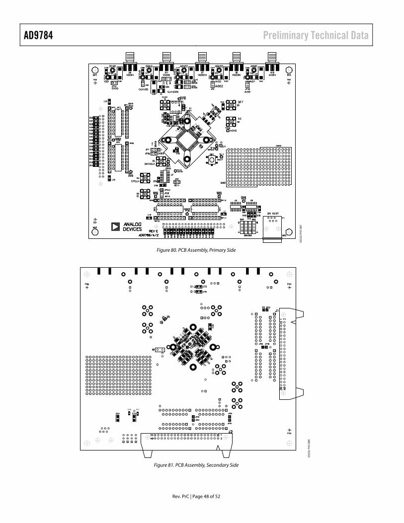
AD9784 Preliminary Technical Data
Rev. PrC | Page 48 of 52
0315
2-Pr
D-0
87
Figure 80. PCB Assembly, Primary Side
0315
2-Pr
D-0
88
Figure 81. PCB Assembly, Secondary Side
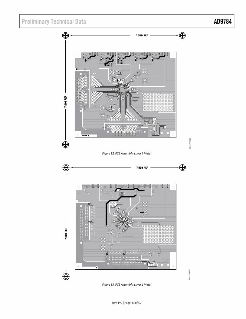
Preliminary Technical Data AD9784
Rev. PrC | Page 49 of 52
0315
2-Pr
D-0
89
Figure 82. PCB Assembly, Layer 1 Metal
0315
2-Pr
D-0
90
Figure 83. PCB Assembly, Layer 6 Metal
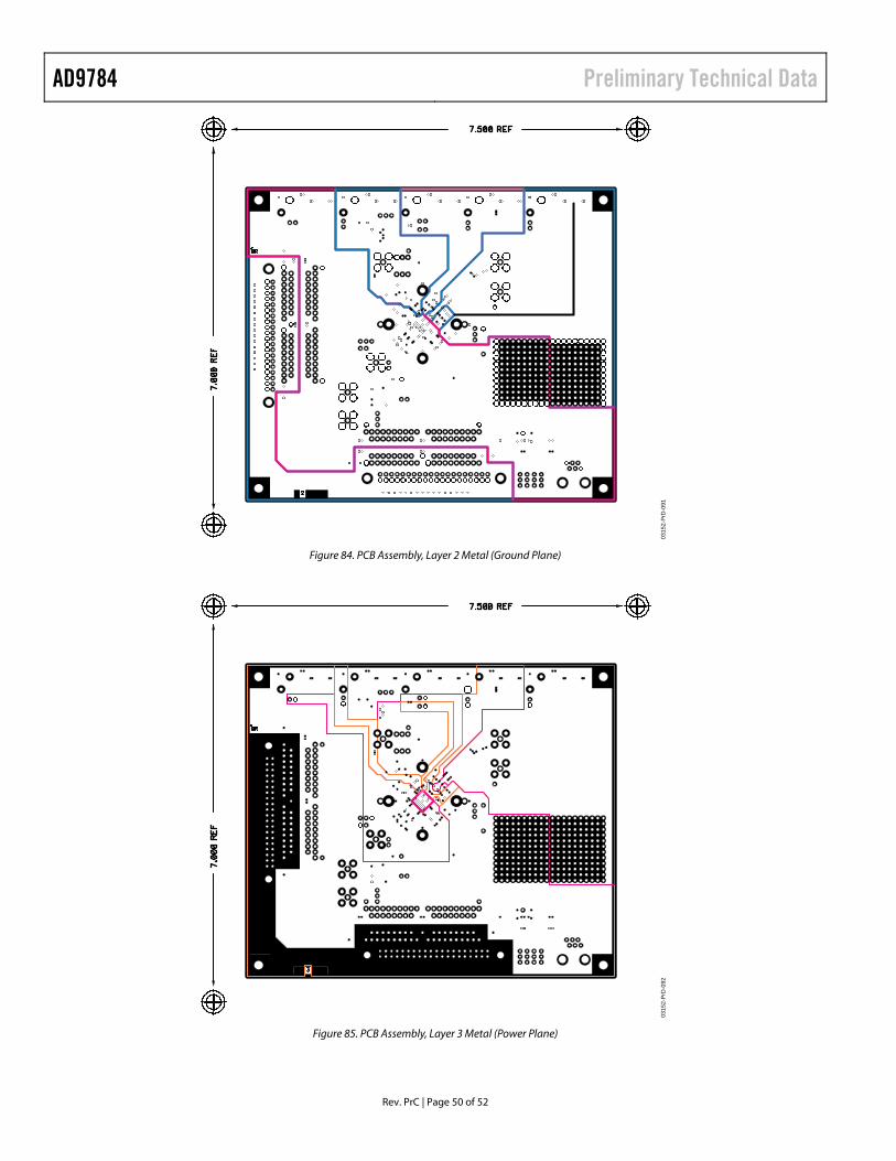
AD9784 Preliminary Technical Data
Rev. PrC | Page 50 of 52
0315
2-Pr
D-0
91
Figure 84. PCB Assembly, Layer 2 Metal (Ground Plane)
0315
2-Pr
D-0
92
Figure 85. PCB Assembly, Layer 3 Metal (Power Plane)
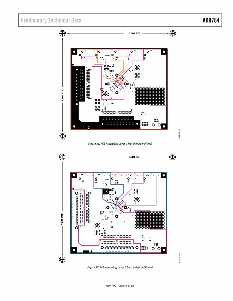
Preliminary Technical Data AD9784
Rev. PrC | Page 51 of 52
0315
2-Pr
D-0
93
Figure 86. PCB Assembly, Layer 4 Metal (Power Plane)
0315
2-Pr
D-0
94
Figure 87. PCB Assembly, Layer 5 Metal (Ground Plane)
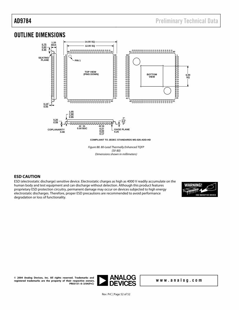
AD9784 Preliminary Technical Data
Rev. PrC | Page 52 of 52
OUTLINE DIMENSIONS
0.150.05
0.270.220.17
0.200.09
0.50 BSC GAGE PLANE0.25
7°3.5°0°
1.051.000.95
1
2021
4140
6080 61
PIN 1
TOP VIEW(PINS DOWN)
14.00 SQ
12.00 SQ
SEATINGPLANE
1.20MAX0.75
0.600.45
1
2021
4140
608061
6.00SQ
BOTTOMVIEW
COPLANARITY0.08
COMPLIANT TO JEDEC STANDARDS MS-026-ADD-HD
Figure 88. 80-Lead Thermally Enhanced TQFP (SV-80)
Dimensions shown in millimeters)
ESD CAUTION ESD (electrostatic discharge) sensitive device. Electrostatic charges as high as 4000 V readily accumulate on the human body and test equipment and can discharge without detection. Although this product features proprietary ESD protection circuitry, permanent damage may occur on devices subjected to high energy electrostatic discharges. Therefore, proper ESD precautions are recommended to avoid performance degradation or loss of functionality.
© 2004 Analog Devices, Inc. All rights reserved. Trademarks and registered trademarks are the property of their respective owners. PR03151–0–3/04(PrC)