Embed Size (px)
Citation preview
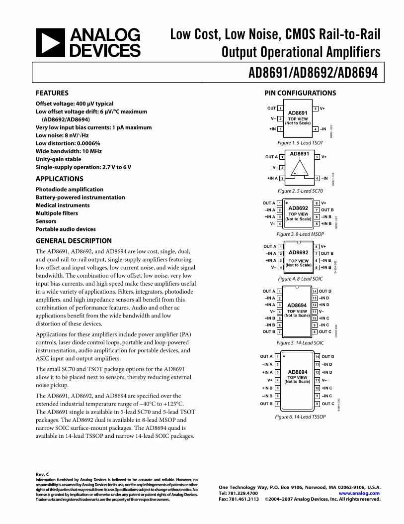
Low Cost, Low Noise, CMOS Rail-to-RailOutput Operational Amplifiers
AD8691/AD8692/AD8694
Rev. C Information furnished by Analog Devices is believed to be accurate and reliable. However, no responsibility is assumed by Analog Devices for its use, nor for any infringements of patents or other rights of third parties that may result from its use. Specifications subject to change without notice. No license is granted by implication or otherwise under any patent or patent rights of Analog Devices. Trademarks and registered trademarks are the property of their respective owners.
One Technology Way, P.O. Box 9106, Norwood, MA 02062-9106, U.S.A.Tel: 781.329.4700 www.analog.com Fax: 781.461.3113 ©2004–2007 Analog Devices, Inc. All rights reserved.
FEATURES Offset voltage: 400 μV typical Low offset voltage drift: 6 μV/°C maximum
(AD8692/AD8694) Very low input bias currents: 1 pA maximum Low noise: 8 nV/√Hz Low distortion: 0.0006% Wide bandwidth: 10 MHz Unity-gain stable Single-supply operation: 2.7 V to 6 V
APPLICATIONS Photodiode amplification Battery-powered instrumentation Medical instruments Multipole filters Sensors Portable audio devices
GENERAL DESCRIPTION The AD8691, AD8692, and AD8694 are low cost, single, dual, and quad rail-to-rail output, single-supply amplifiers featuring low offset and input voltages, low current noise, and wide signal bandwidth. The combination of low offset, low noise, very low input bias currents, and high speed make these amplifiers useful in a wide variety of applications. Filters, integrators, photodiode amplifiers, and high impedance sensors all benefit from this combination of performance features. Audio and other ac applications benefit from the wide bandwidth and low distortion of these devices.
Applications for these amplifiers include power amplifier (PA) controls, laser diode control loops, portable and loop-powered instrumentation, audio amplification for portable devices, and ASIC input and output amplifiers.
The small SC70 and TSOT package options for the AD8691 allow it to be placed next to sensors, thereby reducing external noise pickup.
The AD8691, AD8692, and AD8694 are specified over the extended industrial temperature range of −40°C to +125°C. The AD8691 single is available in 5-lead SC70 and 5-lead TSOT packages. The AD8692 dual is available in 8-lead MSOP and narrow SOIC surface-mount packages. The AD8694 quad is available in 14-lead TSSOP and narrow 14-lead SOIC packages.
PIN CONFIGURATIONS
OUT 1
+IN 3
V– 2
V+5
–IN4
AD8691TOP VIEW
(Not to Scale)
04991-030
Figure 1. 5-Lead TSOT
OUT A 1
V– 2
+IN A 3
V+5
–IN4
AD8691
04991-031
Figure 2. 5-Lead SC70
OUT A 1
–IN A 2
+IN A 3
V– 4
V+8
OUT B7
–IN B6
+IN B5
AD8692TOP VIEW
(Not to Scale)
04991-001
Figure 3. 8-Lead MSOP
OUT A 1
–IN A 2
+IN A 3
V– 4
V+8
OUT B7
–IN B6
+IN B5
AD8692TOP VIEW
(Not to Scale)
04991-002
Figure 4. 8-Lead SOIC
OUT A 1
–IN A 2
+IN A 3
V+ 4
OUT D14
–IN D13
+IN D12
V–11
+IN B 5 +IN C10
–IN B 6 –IN C9
OUT B 7 OUT C8
AD8694TOP VIEW
(Not to Scale)
04991-032
Figure 5. 14-Lead SOIC
04991-033
1
2
3
4
5
6
7
AD8694–IN A
+IN A
V+
OUT B
–IN B
+IN B
OUT A 14
13
12
11
10
9
8
–IN D
+IN D
V–
OUT C
–IN C
+IN C
OUT D
TOP VIEW(Not to Scale)
Figure 6. 14-Lead TSSOP
AD8691/AD8692/AD8694
Rev. C | Page 2 of 12
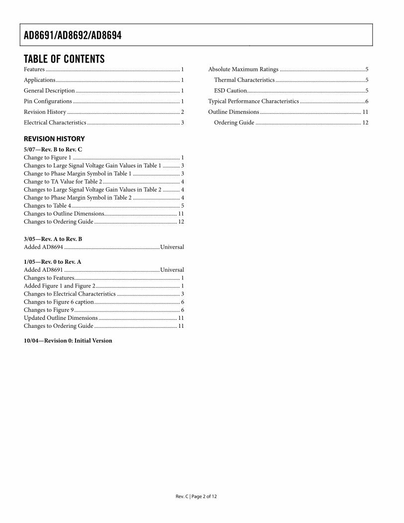
TABLE OF CONTENTS Features .............................................................................................. 1 Applications....................................................................................... 1 General Description ......................................................................... 1 Pin Configurations ........................................................................... 1 Revision History ............................................................................... 2 Electrical Characteristics ................................................................. 3
Absolute Maximum Ratings ............................................................5 Thermal Characteristics ...............................................................5 ESD Caution...................................................................................5
Typical Performance Characteristics ..............................................6 Outline Dimensions ....................................................................... 11
Ordering Guide .......................................................................... 12
REVISION HISTORY 5/07—Rev. B to Rev. C Change to Figure 1 ........................................................................... 1 Changes to Large Signal Voltage Gain Values in Table 1 ............ 3 Change to Phase Margin Symbol in Table 1 ................................. 3 Change to TA Value for Table 2 ...................................................... 4 Changes to Large Signal Voltage Gain Values in Table 2 ............ 4 Change to Phase Margin Symbol in Table 2 ................................. 4 Changes to Table 4............................................................................ 5 Changes to Outline Dimensions................................................... 11 Changes to Ordering Guide .......................................................... 12
3/05—Rev. A to Rev. B Added AD8694 ...................................................................Universal 1/05—Rev. 0 to Rev. A Added AD8691 ...................................................................Universal Changes to Features.......................................................................... 1 Added Figure 1 and Figure 2........................................................... 1 Changes to Electrical Characteristics ............................................ 3 Changes to Figure 6 caption............................................................ 6 Changes to Figure 9.......................................................................... 6 Updated Outline Dimensions ....................................................... 11 Changes to Ordering Guide .......................................................... 11 10/04—Revision 0: Initial Version
AD8691/AD8692/AD8694
Rev. C | Page 3 of 12
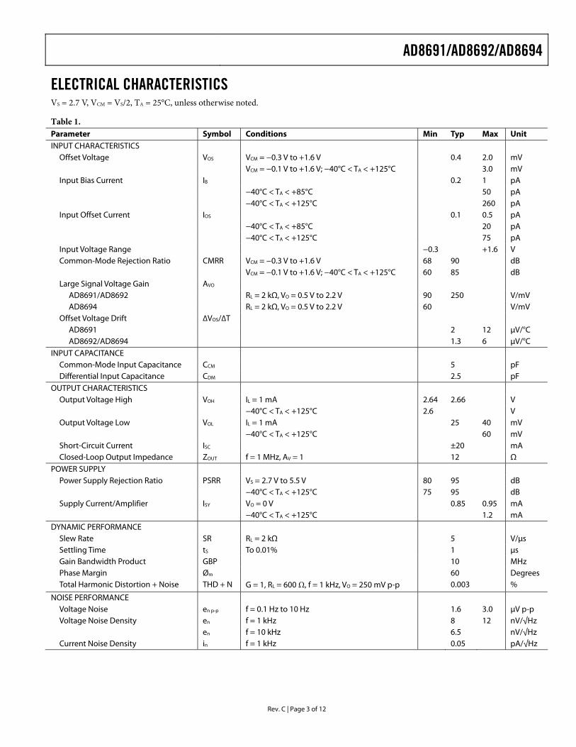
ELECTRICAL CHARACTERISTICS VS = 2.7 V, VCM = VS/2, TA = 25°C, unless otherwise noted.
Table 1. Parameter Symbol Conditions Min Typ Max Unit INPUT CHARACTERISTICS
Offset Voltage VOS VCM = −0.3 V to +1.6 V 0.4 2.0 mV VCM = −0.1 V to +1.6 V; −40°C < TA < +125°C 3.0 mV Input Bias Current IB 0.2 1 pA −40°C < TA < +85°C 50 pA −40°C < TA < +125°C 260 pA Input Offset Current IOS 0.1 0.5 pA −40°C < TA < +85°C 20 pA −40°C < TA < +125°C 75 pA Input Voltage Range −0.3 +1.6 V Common-Mode Rejection Ratio CMRR VCM = −0.3 V to +1.6 V 68 90 dB VCM = −0.1 V to +1.6 V; −40°C < TA < +125°C 60 85 dB Large Signal Voltage Gain AVO
AD8691/AD8692 RL = 2 kΩ, VO = 0.5 V to 2.2 V 90 250 V/mV AD8694 RL = 2 kΩ, VO = 0.5 V to 2.2 V 60 V/mV
Offset Voltage Drift ∆VOS/∆T AD8691 2 12 μV/°C AD8692/AD8694 1.3 6 μV/°C
INPUT CAPACITANCE Common-Mode Input Capacitance CCM 5 pF Differential Input Capacitance CDM 2.5 pF
OUTPUT CHARACTERISTICS Output Voltage High VOH IL = 1 mA 2.64 2.66 V −40°C < TA < +125°C 2.6 V Output Voltage Low VOL IL = 1 mA 25 40 mV −40°C < TA < +125°C 60 mV Short-Circuit Current ISC ±20 mA Closed-Loop Output Impedance ZOUT f = 1 MHz, AV = 1 12 Ω
POWER SUPPLY Power Supply Rejection Ratio PSRR VS = 2.7 V to 5.5 V 80 95 dB −40°C < TA < +125°C 75 95 dB Supply Current/Amplifier ISY VO = 0 V 0.85 0.95 mA −40°C < TA < +125°C 1.2 mA
DYNAMIC PERFORMANCE Slew Rate SR RL = 2 kΩ 5 V/μs Settling Time tS To 0.01% 1 μs Gain Bandwidth Product GBP 10 MHz Phase Margin Øm 60 Degrees Total Harmonic Distortion + Noise THD + N G = 1, RL = 600 Ω, f = 1 kHz, VO = 250 mV p-p 0.003 %
NOISE PERFORMANCE Voltage Noise en p-p f = 0.1 Hz to 10 Hz 1.6 3.0 μV p-p Voltage Noise Density en f = 1 kHz 8 12 nV/√Hz en f = 10 kHz 6.5 nV/√Hz Current Noise Density in f = 1 kHz 0.05 pA/√Hz
AD8691/AD8692/AD8694
Rev. C | Page 4 of 12
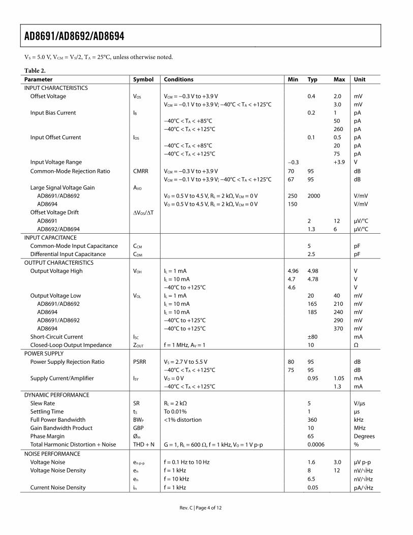
VS = 5.0 V, VCM = VS/2, TA = 25°C, unless otherwise noted.
Table 2. Parameter Symbol Conditions Min Typ Max Unit INPUT CHARACTERISTICS
Offset Voltage VOS VCM = −0.3 V to +3.9 V 0.4 2.0 mV VCM = −0.1 V to +3.9 V; −40°C < TA < +125°C 3.0 mV Input Bias Current IB 0.2 1 pA −40°C < TA < +85°C 50 pA −40°C < TA < +125°C 260 pA Input Offset Current IOS 0.1 0.5 pA −40°C < TA < +85°C 20 pA −40°C < TA < +125°C 75 pA Input Voltage Range −0.3 +3.9 V
Common-Mode Rejection Ratio CMRR VCM = −0.3 V to +3.9 V 70 95 dB VCM = −0.1 V to +3.9 V; −40°C < TA < +125°C 67 95 dB Large Signal Voltage Gain AVO
AD8691/AD8692 VO = 0.5 V to 4.5 V, RL = 2 kΩ, VCM = 0 V 250 2000 V/mV AD8694 VO = 0.5 V to 4.5 V, RL = 2 kΩ, VCM = 0 V 150 V/mV
Offset Voltage Drift ∆VOS/∆T AD8691 2 12 μV/°C AD8692/AD8694 1.3 6 μV/°C
INPUT CAPACITANCE Common-Mode Input Capacitance CCM 5 pF Differential Input Capacitance CDM 2.5 pF
OUTPUT CHARACTERISTICS Output Voltage High VOH IL = 1 mA 4.96 4.98 V IL = 10 mA 4.7 4.78 V −40°C to +125°C 4.6 V Output Voltage Low VOL IL = 1 mA 20 40 mV
AD8691/AD8692 IL = 10 mA 165 210 mV AD8694 IL = 10 mA 185 240 mV AD8691/AD8692 −40°C to +125°C 290 mV AD8694 −40°C to +125°C 370 mV
Short-Circuit Current ISC ±80 mA Closed-Loop Output Impedance ZOUT f = 1 MHz, AV = 1 10 Ω
POWER SUPPLY Power Supply Rejection Ratio PSRR VS = 2.7 V to 5.5 V 80 95 dB −40°C < TA < +125°C 75 95 dB Supply Current/Amplifier ISY VO = 0 V 0.95 1.05 mA −40°C < TA < +125°C 1.3 mA
DYNAMIC PERFORMANCE Slew Rate SR RL = 2 kΩ 5 V/μs Settling Time tS To 0.01% 1 μs Full Power Bandwidth BWP <1% distortion 360 kHz Gain Bandwidth Product GBP 10 MHz Phase Margin Øm 65 Degrees Total Harmonic Distortion + Noise THD + N G = 1, RL = 600 Ω, f = 1 kHz, VO = 1 V p-p 0.0006 %
NOISE PERFORMANCE Voltage Noise en p-p f = 0.1 Hz to 10 Hz 1.6 3.0 μV p-p Voltage Noise Density en f = 1 kHz 8 12 nV/√Hz en f = 10 kHz 6.5 nV/√Hz Current Noise Density in f = 1 kHz 0.05 pA/√Hz
AD8691/AD8692/AD8694
Rev. C | Page 5 of 12
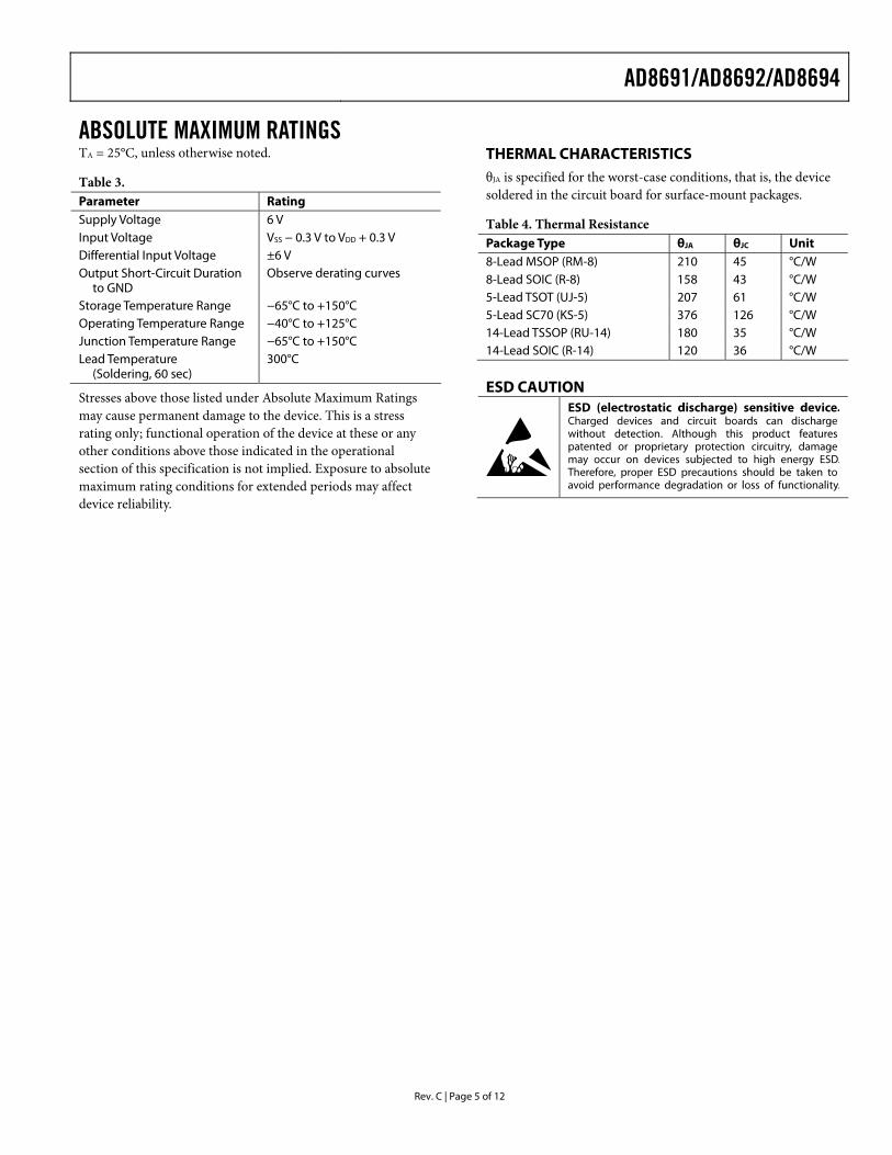
ABSOLUTE MAXIMUM RATINGS TA = 25°C, unless otherwise noted.
Table 3. Parameter Rating Supply Voltage 6 V Input Voltage VSS − 0.3 V to VDD + 0.3 V Differential Input Voltage ±6 V Output Short-Circuit Duration
to GND Observe derating curves
Storage Temperature Range −65°C to +150°C Operating Temperature Range −40°C to +125°C Junction Temperature Range −65°C to +150°C Lead Temperature
(Soldering, 60 sec) 300°C
Stresses above those listed under Absolute Maximum Ratings may cause permanent damage to the device. This is a stress rating only; functional operation of the device at these or any other conditions above those indicated in the operational section of this specification is not implied. Exposure to absolute maximum rating conditions for extended periods may affect device reliability.
THERMAL CHARACTERISTICS θJA is specified for the worst-case conditions, that is, the device soldered in the circuit board for surface-mount packages.
Table 4. Thermal Resistance Package Type θJA θJC Unit 8-Lead MSOP (RM-8) 210 45 °C/W 8-Lead SOIC (R-8) 158 43 °C/W 5-Lead TSOT (UJ-5) 207 61 °C/W 5-Lead SC70 (KS-5) 376 126 °C/W 14-Lead TSSOP (RU-14) 180 35 °C/W 14-Lead SOIC (R-14) 120 36 °C/W
ESD CAUTION
AD8691/AD8692/AD8694
Rev. C | Page 6 of 12
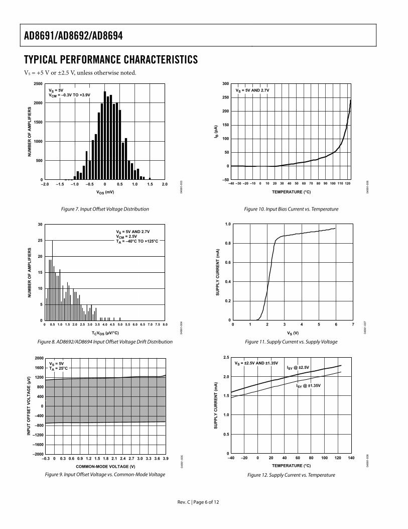
TYPICAL PERFORMANCE CHARACTERISTICS VS = +5 V or ±2.5 V, unless otherwise noted.
NU
MB
ER O
F A
MPL
IFIE
RS
VOS (mV) 04991-0030
500
1000
1500
2000
2500
–2.0 –1.5 –1.0 –0.5 0 0.5 1.0 1.5 2.0
VS = 5VVCM = –0.3V TO +3.9V
Figure 7. Input Offset Voltage Distribution
NU
MB
ER O
F A
MPL
IFIE
RS
TCVOS (µV/°C) 04991-0040
5
10
15
20
25
30
VS = 5V AND 2.7VVCM = 2.5VTA = –40°C TO +125°C
4.0 4.5 5.0 5.5 6.0 6.5 7.0 7.5 8.00 0.5 1.0 1.5 2.0 2.5 3.0 3.5
Figure 8. AD8692/AD8694 Input Offset Voltage Drift Distribution
–2000
–1600
–1200
–800
–400
0
400
800
1200
1600
2000
INPU
T O
FFSE
T VO
LTA
GE
(µV)
–0.3 0 0.3 0.6 0.9 1.2 1.8 3.01.5 2.1 2.4 2.7 3.63.3 3.9
COMMON-MODE VOLTAGE (V) 04991-005
VS = 5VTA = 25°C
Figure 9. Input Offset Voltage vs. Common-Mode Voltage
I B (p
A)
TEMPERATURE (°C) 04991-006–50
0
50
100
150
200
250
300
–40 –20 0 20 40 60 80 100 120–10 10 30 50 70 90 110–30
VS = 5V AND 2.7V
Figure 10. Input Bias Current vs. Temperature
0
0.2
0.4
0.6
0.8
1.0SU
PPLY
CU
RR
ENT
(mA
)
0 1 2 3 4 5 6 7
VS (V) 04991-007
Figure 11. Supply Current vs. Supply Voltage
0
0.5
1.0
1.5
2.0
2.5
SUPP
LY C
UR
REN
T (m
A)
–40 –20 0 20 40 60 80 100 120 140
TEMPERATURE (°C) 04991-008
VS = ±2.5V AND ±1.35VISY @ ±2.5V
ISY @ ±1.35V
Figure 12. Supply Current vs. Temperature
AD8691/AD8692/AD8694
Rev. C | Page 7 of 12
0.1
1
10
100
1000
10000
0.001 0.01 0.1 1 10 100
OU
TPU
T VO
LTA
GE
TO S
UPP
LY R
AIL
(mV)
LOAD CURRENT (mA) 04991-009
AD8691_92 SOURCE
AD8694 SOURCE
AD8694 SINK
AD8691_92 SINK
VS = 5V
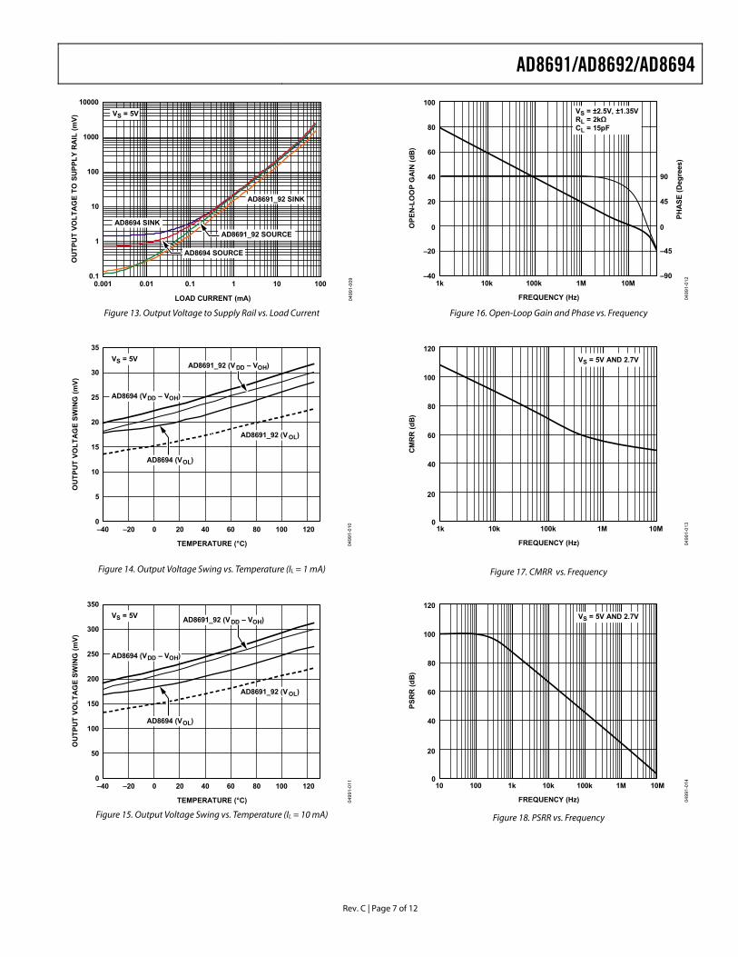
Figure 13. Output Voltage to Supply Rail vs. Load Current
0
5
10
15
20
25
30
35
OU
TPU
T VO
LTA
GE
SWIN
G (m
V)
–40 –20 0 20 40 60 80 100 120
TEMPERATURE (°C) 04991-010
VS = 5V
AD8691_92 (VOL)
AD8694 (VDD – VOH)
AD8694 (VOL)
AD8691_92 (VDD – VOH)
Figure 14. Output Voltage Swing vs. Temperature (IL = 1 mA)
0
50
100
150
200
250
300
350
OU
TPU
T VO
LTA
GE
SWIN
G (m
V)
–40 –20 0 20 40 60 80 100 120
TEMPERATURE (°C) 04991-011
VS = 5V
AD8691_92 (VOL)
AD8694 (VDD – VOH)
AD8694 (VOL)
AD8691_92 (VDD – VOH)
Figure 15. Output Voltage Swing vs. Temperature (IL = 10 mA)
1k 10k 100k 1M 10M
OPE
N-L
OO
P G
AIN
(dB
)
FREQUENCY (Hz) 04991-012–40
–20
20
40
60
80
100
0
PHA
SE (D
egre
es)
–90
–45
45
90
0
VS = ±2.5V, ±1.35VRL = 2kΩCL = 15pF
Figure 16. Open-Loop Gain and Phase vs. Frequency
1k 10k 100k 1M 10M
CM
RR
(dB
)
FREQUENCY (Hz) 04991-0130
40
60
80
100
120
20
VS = 5V AND 2.7V
Figure 17. CMRR vs. Frequency
PSR
R (d
B)
FREQUENCY (Hz) 04991-0140
40
60
80
100
120
20
10 100 1k 10k 100k 1M 10M
VS = 5V AND 2.7V
Figure 18. PSRR vs. Frequency
AD8691/AD8692/AD8694
Rev. C | Page 8 of 12
0.0001
0.001
0.01
0.1
1
10
100
1000
10000
100 1k 10k 100k 1M 10M
IMPE
DA
NC
E (Ω
)
FREQUENCY (Hz) 04991-015
VS = ±2.5V
AV = 100
AV = 10
AV = 1
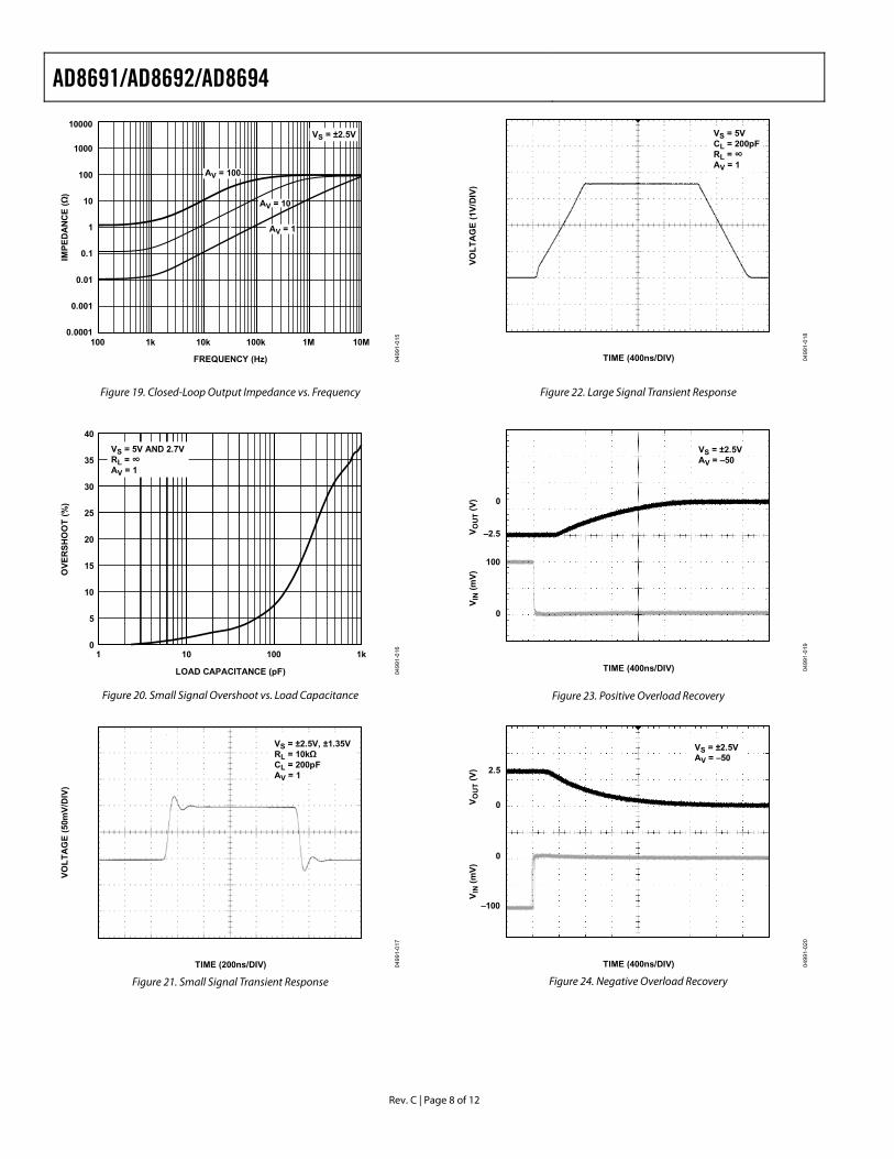
Figure 19. Closed-Loop Output Impedance vs. Frequency
OVE
RSH
OO
T (%
)
1 10 100 1k
LOAD CAPACITANCE (pF) 04991-0160
5
10
15
20
25
30
35
40VS = 5V AND 2.7VRL = ∞AV = 1
Figure 20. Small Signal Overshoot vs. Load Capacitance
VOLT
AG
E (5
0mV/
DIV
)
TIME (200ns/DIV) 04991-017
VS = ±2.5V, ±1.35VRL = 10kΩCL = 200pFAV = 1
Figure 21. Small Signal Transient Response
VOLT
AG
E (1
V/D
IV)
TIME (400ns/DIV) 04991-018
VS = 5VCL = 200pFRL = ∞AV = 1
Figure 22. Large Signal Transient Response
V OU
T (V
)
TIME (400ns/DIV) 04991-019
VS = ±2.5VAV = –50
–2.5
100
0
0
V IN
(mV)
Figure 23. Positive Overload Recovery
V OU
T (V
)
TIME (400ns/DIV) 04991-020
VS = ±2.5VAV = –50
2.5
–100
0
0
V IN
(mV)
Figure 24. Negative Overload Recovery
AD8691/AD8692/AD8694
Rev. C | Page 9 of 12
0.0001
0.001
0.01
THD
+ N
(%)
20 100 1k 10k 20k
FREQUENCY (Hz) 04991-021
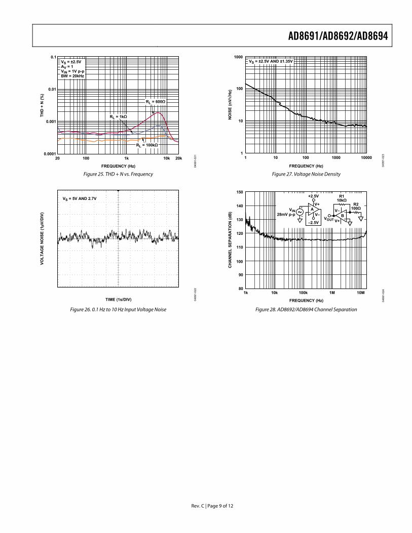
0.1VS = ±2.5VAV = 1VIN = 1V p-pBW = 20kHz
RL = 1kΩ
RL = 600Ω
RL = 100kΩ
Figure 25. THD + N vs. Frequency
VOLT
AG
E N
OIS
E (1
µV/D
IV)
TIME (1s/DIV) 04991-022
VS = 5V AND 2.7V
Figure 26. 0.1 Hz to 10 Hz Input Voltage Noise
NO
ISE
(nV/
Hz)
1
100
10
1000
FREQUENCY (Hz)
101 100 1000 10000
04991-023
VS = ±2.5V AND ±1.35V
Figure 27. Voltage Noise Density
1k 10k 100k 1M 10M
CH
AN
NEL
SEP
AR
ATI
ON
(dB
)
FREQUENCY (Hz) 04991-02480
90
110
120
130
140
150
100
VIN28mV p-p V–
–2.5V
V+
+2.5V
ABVOUT V+
V–
R110kΩ
R2100Ω
Figure 28. AD8692/AD8694 Channel Separation
AD8691/AD8692/AD8694
Rev. C | Page 10 of 12
VS = +2.7 V or ±1.35 V, unless otherwise noted.
NU
MB
ER O
F A
MPL
IFIE
RS
VOS (mV) 04991-0250
200
400
600
800
1000
1200
–2.0 –1.5 –1.0 –0.5 0 0.5 1.0 1.5 2.0
VS = 2.7VVCM = –0.3V TO +1.6V
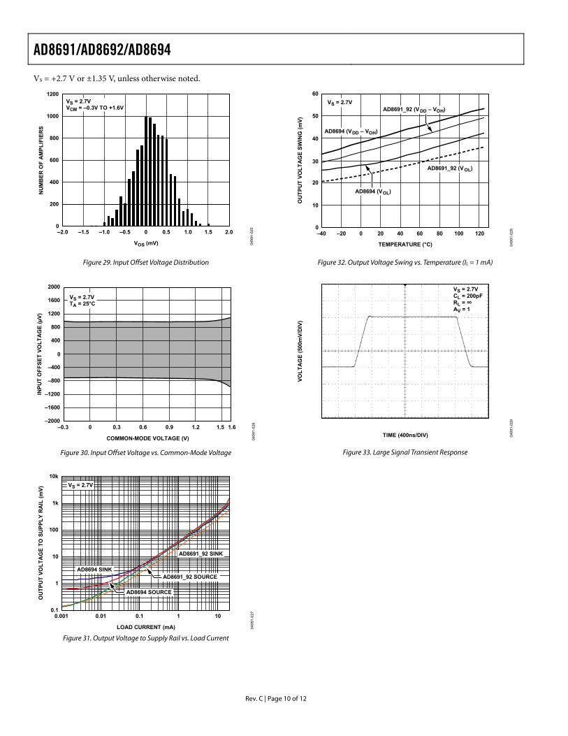
Figure 29. Input Offset Voltage Distribution
INPU
T O
FFSE
T VO
LTA
GE
(µV)
COMMON-MODE VOLTAGE (V) 04991-026–2000
–1600
–1200
–800
–400
400
800
1200
1600
2000
–0.3 0 0.3 0.6 0.9 1.2 1.5 1.6
0
VS = 2.7VTA = 25°C
Figure 30. Input Offset Voltage vs. Common-Mode Voltage
0.1
1
10
100
1k
10k
0.001 0.01 0.1 1 10
OU
TPU
T VO
LTA
GE
TO S
UPP
LY R
AIL
(mV)
LOAD CURRENT (mA) 04991-027
AD8691_92 SOURCE
AD8694 SOURCE
AD8694 SINK
AD8691_92 SINK
VS = 2.7V
Figure 31. Output Voltage to Supply Rail vs. Load Current
0
10
20
30
40
50
60
OU
TPU
T VO
LTA
GE
SWIN
G (m
V)
–40 –20 0 20 40 60 80 100 120
TEMPERATURE (°C) 04991-028
VS = 2.7V
AD8691_92 (VOL)
AD8694 (VDD – VOH)
AD8694 (VOL)
AD8691_92 (VDD – VOH)
Figure 32. Output Voltage Swing vs. Temperature (IL = 1 mA)
VOLT
AG
E (5
00m
V/D
IV)
TIME (400ns/DIV) 04991-029
VS = 2.7VCL = 200pFRL = ∞AV = 1
Figure 33. Large Signal Transient Response
AD8691/AD8692/AD8694
Rev. C | Page 11 of 12
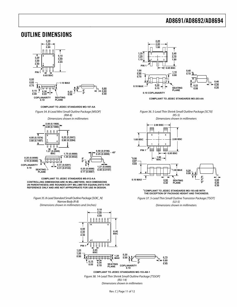
OUTLINE DIMENSIONS
COMPLIANT TO JEDEC STANDARDS MO-187-AA
0.800.600.40
8°0°
4
8
1
5
PIN 10.65 BSC
SEATINGPLANE
0.380.22
1.10 MAX
3.203.002.80
COPLANARITY0.10
0.230.08
3.203.002.80
5.154.904.65
0.150.00
0.950.850.75
Figure 34. 8-Lead Mini Small Outline Package [MSOP]
(RM-8) Dimensions shown in millimeters
CONTROLLING DIMENSIONS ARE IN MILLIMETERS; INCH DIMENSIONS(IN PARENTHESES) ARE ROUNDED-OFF MILLIMETER EQUIVALENTS FORREFERENCE ONLY AND ARE NOT APPROPRIATE FOR USE IN DESIGN.
COMPLIANT TO JEDEC STANDARDS MS-012-AA
0.25 (0.0098)0.17 (0.0067)
1.27 (0.0500)0.40 (0.0157)
0.50 (0.0196)0.25 (0.0099)
45°
8°0°
1.75 (0.0688)1.35 (0.0532)
SEATINGPLANE
0.25 (0.0098)0.10 (0.0040)
41
8 5
5.00 (0.1968)4.80 (0.1890)
4.00 (0.1574)3.80 (0.1497)
1.27 (0.0500)BSC
6.20 (0.2441)5.80 (0.2284)
0.51 (0.0201)0.31 (0.0122)
COPLANARITY0.10
Figure 35. 8-Lead Standard Small Outline Package [SOIC_N] Narrow Body (R-8)
Dimensions shown in millimeters and (inches)
COMPLIANT TO JEDEC STANDARDS MO-203-AA
0.300.15
0.10 MAX
1.000.900.70
0.460.360.26SEATING
PLANE
0.220.08
1.100.80
45
1 2 3
PIN 10.65 BSC
2.202.001.80
2.402.101.80
1.351.251.15
0.10 COPLANARITY
0.400.10
Figure 36. 5-Lead Thin Shrink Small Outline Package [SC70] (KS-5)
Dimensions shown in millimeters
*COMPLIANT TO JEDEC STANDARDS MO-193-AB WITHTHE EXCEPTION OF PACKAGE HEIGHT AND THICKNESS.
PIN 1
1.60 BSC 2.80 BSC
1.90BSC
0.95 BSC
0.200.08
0.600.450.30
8°4°0°
0.500.30
0.10 MAX SEATINGPLANE
*1.00 MAX
*0.900.870.84
2.90 BSC
5 4
1 2 3
Figure 37. 5-Lead Thin Small Outline Transistor Package [TSOT]
(UJ-5) Dimensions shown in millimeters
4.504.404.30
14 8
71
6.40BSC
PIN 1
5.105.004.90
0.65BSC
SEATINGPLANE
0.150.05
0.300.19
1.20MAX
1.051.000.80
0.200.09
8°0°
0.750.600.45
COPLANARITY0.10
COMPLIANT TO JEDEC STANDARDS MO-153-AB-1 Figure 38. 14-Lead Thin Shrink Small Outline Package [TSSOP]
(RU-14) Dimensions shown in millimeters
AD8691/AD8692/AD8694
Rev. C | Page 12 of 12
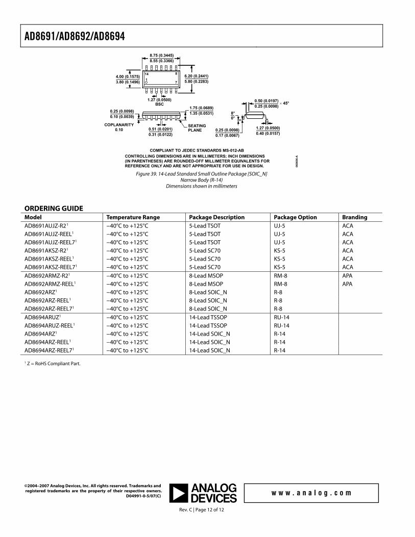
CONTROLLING DIMENSIONS ARE IN MILLIMETERS; INCH DIMENSIONS(IN PARENTHESES) ARE ROUNDED-OFF MILLIMETER EQUIVALENTS FORREFERENCE ONLY AND ARE NOT APPROPRIATE FOR USE IN DESIGN.
COMPLIANT TO JEDEC STANDARDS MS-012-AB
0606
06-A
14 8
71
6.20 (0.2441)5.80 (0.2283)
4.00 (0.1575)3.80 (0.1496)
8.75 (0.3445)8.55 (0.3366)
1.27 (0.0500)BSC
SEATINGPLANE
0.25 (0.0098)0.10 (0.0039)
0.51 (0.0201)0.31 (0.0122)
1.75 (0.0689)1.35 (0.0531)
0.50 (0.0197)0.25 (0.0098)
1.27 (0.0500)0.40 (0.0157)
0.25 (0.0098)0.17 (0.0067)
COPLANARITY0.10
8°0°
45°
Figure 39. 14-Lead Standard Small Outline Package [SOIC_N]
Narrow Body (R-14) Dimensions shown in millimeters
ORDERING GUIDE Model Temperature Range Package Description Package Option Branding AD8691AUJZ-R21 −40°C to +125°C 5-Lead TSOT UJ-5 ACA AD8691AUJZ-REEL1 −40°C to +125°C 5-Lead TSOT UJ-5 ACA AD8691AUJZ-REEL71 −40°C to +125°C 5-Lead TSOT UJ-5 ACA AD8691AKSZ-R21 −40°C to +125°C 5-Lead SC70 KS-5 ACA AD8691AKSZ-REEL1 −40°C to +125°C 5-Lead SC70 KS-5 ACA AD8691AKSZ-REEL71 −40°C to +125°C 5-Lead SC70 KS-5 ACA AD8692ARMZ-R21 −40°C to +125°C 8-Lead MSOP RM-8 APA AD8692ARMZ-REEL1 −40°C to +125°C 8-Lead MSOP RM-8 APA AD8692ARZ1 −40°C to +125°C 8-Lead SOIC_N R-8 AD8692ARZ-REEL1 −40°C to +125°C 8-Lead SOIC_N R-8 AD8692ARZ-REEL71 −40°C to +125°C 8-Lead SOIC_N R-8 AD8694ARUZ1 −40°C to +125°C 14-Lead TSSOP RU-14 AD8694ARUZ-REEL1 −40°C to +125°C 14-Lead TSSOP RU-14 AD8694ARZ1 −40°C to +125°C 14-Lead SOIC_N R-14 AD8694ARZ-REEL1 −40°C to +125°C 14-Lead SOIC_N R-14 AD8694ARZ-REEL71 −40°C to +125°C 14-Lead SOIC_N R-14 1 Z = RoHS Compliant Part.
©2004–2007 Analog Devices, Inc. All rights reserved. Trademarks and registered trademarks are the property of their respective owners. D04991-0-5/07(C)