Embed Size (px)
Citation preview
Audio/Video, 60 MHz, 16 × 8, Gain of +2 Crosspoint Switch
AD8112
Rev. 0 Information furnished by Analog Devices is believed to be accurate and reliable. However, no responsibility is assumed by Analog Devices for its use, nor for any infringements of patents or other rights of third parties that may result from its use. Specifications subject to change without notice. No license is granted by implication or otherwise under any patent or patent rights of Analog Devices. Trademarks and registered trademarks are the property of their respective owners.
One Technology Way, P.O. Box 9106, Norwood, MA 02062-9106, U.S.A.Tel: 781.329.4700 www.analog.com Fax: 781.461.3113 ©2007 Analog Devices, Inc. All rights reserved.
FEATURES Low cost, 16 × 8, high speed, nonblocking switch array
Pin-compatible 16 × 16 version available (AD8113) Serial or parallel programming of switch array Serial data out allows daisy chaining control of multiple
16 × 8 arrays to create larger switch arrays Output disable allows connection of multiple devices
without loading the output bus Complete solution
Buffered inputs 8 output amplifiers Operates on ±5 V or ±12 V supplies Low supply current of 54 mA
Excellent audio performance VS = ±12 V ±10 V output swing 0.002% THD at 20 kHz maximum 20 V p-p (RL = 600 Ω)
Excellent video performance VS = ±5 V 0.1 dB gain flatness of 10 MHz 0.1% differential gain error (RL = 1 kΩ) 0.1° differential phase error (RL = 1 kΩ)
Excellent ac performance −3 dB bandwidth 60 MHz
Low all-hostile crosstalk of −83 dB at 20 kHz Reset pin allows disabling of all outputs (connected to a
capacitor to ground provides power-on reset capability) 100-lead LQFP (14 mm × 14 mm)
APPLICATIONS CCTV surveillance/DVR Analog/digital audio routers Video routers (NTSC, PAL, S-Video, SECAM) Multimedia systems Video conferencing
FUNCTIONAL BLOCK DIAGRAM
0652
3-00
1
AD8112
40 40
40
128
PARALLEL LATCH
8
CLK
DATA IN
CE
RESET
16 IN
PUTS
A0
DATAOUT
8 O
UTP
UTS
A1A2
D0 D1 D2 D3 D4
ENA
BLE
/DIS
AB
LE
SWITCHMATRIX
SER/PAR
UPDATE
DECODE8 × 5:16 DECODERS
80-BIT SHIFT REGISTERWITH 5-BIT
PARALLEL LOADING
OUTPUTBUFFERG = +2 SE
T IN
DIV
IDU
AL
OR
RES
ET A
LL O
UTP
UTS
TO O
FF
NOCONNECT
Figure 1.
GENERAL DESCRIPTION The AD8112 is a low cost, fully buffered crosspoint switch matrix that operates on ±12 V for audio applications and ±5 V for video applications. It offers a −3 dB signal bandwidth greater than 60 MHz and channel switch times of less than 60 ns with 0.1% settling for use in both analog and digital audio. The AD8112 operated at 20 kHz has a crosstalk performance of −83 dB and isolation of 90 dB. In addition, ground/power pins surround all inputs and outputs to provide extra shielding for operation in the most demanding audio routing applications. With a differential gain and differential phase better than 0.1% and 0.1°, respectively, and a 0.1 dB flatness output of up to 10 MHz, the AD8112 is suitable for many video applications.
The AD8112 includes eight independent output buffers that can be placed into a disabled state for paralleling crosspoint outputs so that off channel loading is minimized. The AD8112 has a gain of +2. It operates on voltage supplies of ±5 V or ±12 V while consuming only 34 mA or 31 mA of current, respectively. The channel switching is performed via a serial digital control (which can accommodate the daisy chaining of several devices) or via a parallel control, allowing updating of an individual output without reprogramming the entire array.
The AD8112 is packaged in a 100-lead LQFP and is available over the commercial temperature range of 0°C to 70°C.
AD8112
Rev. 0 | Page 2 of 28
TABLE OF CONTENTS Features .............................................................................................. 1
Applications....................................................................................... 1
Functional Block Diagram .............................................................. 1
General Description ......................................................................... 1
Revision History ............................................................................... 2
Specifications..................................................................................... 3
Timing Characteristics (Serial) .................................................. 5
Timing Characteristics (Parallel) ............................................... 6
Absolute Maximum Ratings............................................................ 7
ESD Caution.................................................................................. 7
Power Dissipation......................................................................... 7
Pin Configuration and Function Descriptions............................. 9
I/O Schematics............................................................................ 11
Typical Performance Characteristics ........................................... 12
Theory of Operation ...................................................................... 17
Calculation of Power Dissipation............................................. 17
Short-Circuit Output Conditions............................................. 18
Application Notes ........................................................................... 19
Serial Programming................................................................... 19
Parallel Programming................................................................ 19
Power-On Reset .......................................................................... 20
Specifying Audio Levels ............................................................ 20
Creating Unity-Gain Channels................................................. 20
Video Signals............................................................................... 20
Creating Larger Crosspoint Arrays.......................................... 21
Multichannel Video and Audio ................................................ 23
Crosstalk ...................................................................................... 23
PCB Layout...................................................................................... 26
Outline Dimensions ....................................................................... 28
Ordering Guide .......................................................................... 28
REVISION HISTORY
2/07—Revision 0: Initial Version
AD8112
Rev. 0 | Page 3 of 28
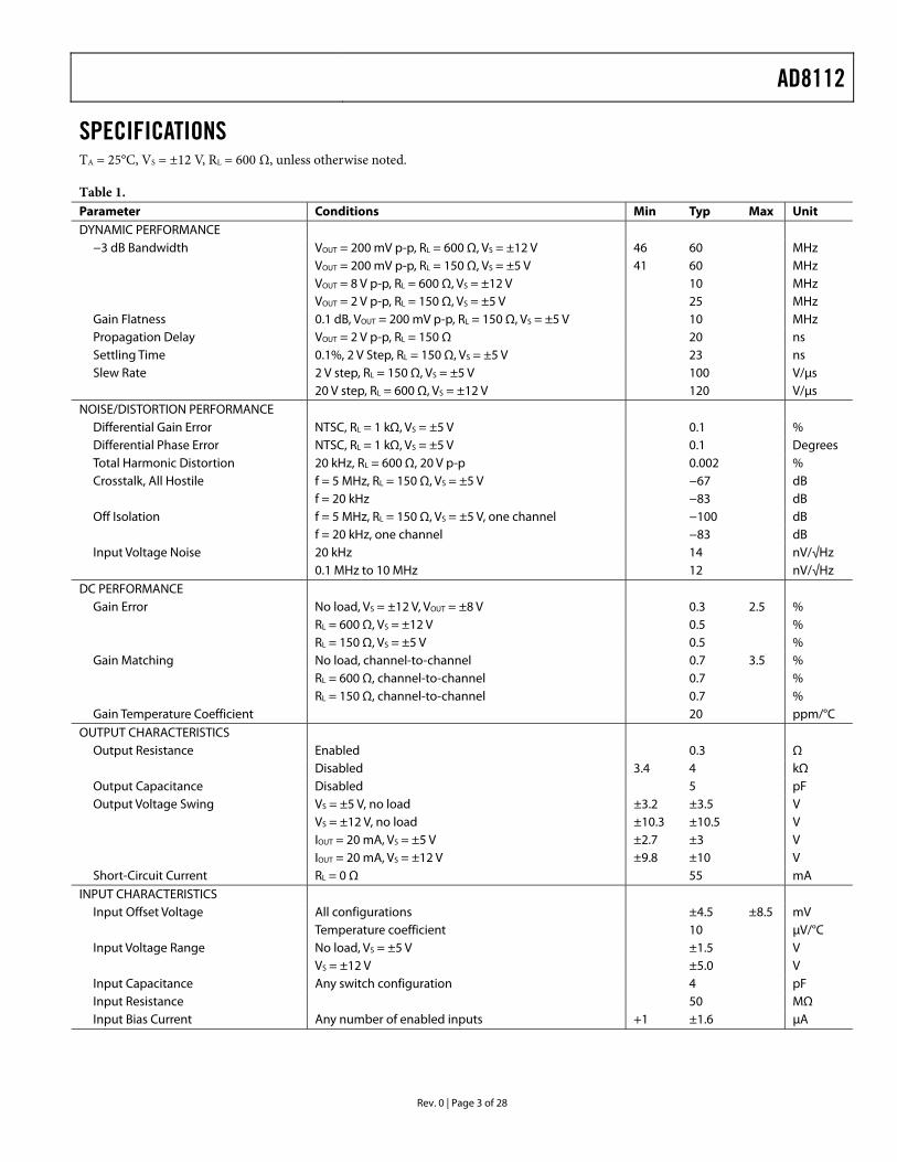
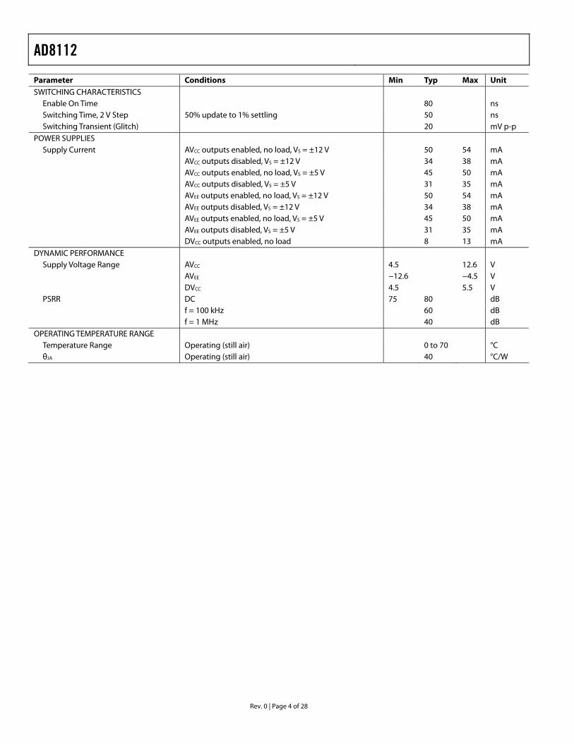
SPECIFICATIONS TA = 25°C, VS = ±12 V, RL = 600 Ω, unless otherwise noted.
Table 1. Parameter Conditions Min Typ Max Unit DYNAMIC PERFORMANCE
−3 dB Bandwidth VOUT = 200 mV p-p, RL = 600 Ω, VS = ±12 V 46 60 MHz VOUT = 200 mV p-p, RL = 150 Ω, VS = ±5 V 41 60 MHz VOUT = 8 V p-p, RL = 600 Ω, VS = ±12 V 10 MHz VOUT = 2 V p-p, RL = 150 Ω, VS = ±5 V 25 MHz Gain Flatness 0.1 dB, VOUT = 200 mV p-p, RL = 150 Ω, VS = ±5 V 10 MHz Propagation Delay VOUT = 2 V p-p, RL = 150 Ω 20 ns Settling Time 0.1%, 2 V Step, RL = 150 Ω, VS = ±5 V 23 ns Slew Rate 2 V step, RL = 150 Ω, VS = ±5 V 100 V/μs 20 V step, RL = 600 Ω, VS = ±12 V 120 V/μs
NOISE/DISTORTION PERFORMANCE Differential Gain Error NTSC, RL = 1 kΩ, VS = ±5 V 0.1 % Differential Phase Error NTSC, RL = 1 kΩ, VS = ±5 V 0.1 Degrees Total Harmonic Distortion 20 kHz, RL = 600 Ω, 20 V p-p 0.002 % Crosstalk, All Hostile f = 5 MHz, RL = 150 Ω, VS = ±5 V −67 dB f = 20 kHz −83 dB Off Isolation f = 5 MHz, RL = 150 Ω, VS = ±5 V, one channel −100 dB f = 20 kHz, one channel −83 dB Input Voltage Noise 20 kHz 14 nV/√Hz 0.1 MHz to 10 MHz 12 nV/√Hz
DC PERFORMANCE Gain Error No load, VS = ±12 V, VOUT = ±8 V 0.3 2.5 % RL = 600 Ω, VS = ±12 V 0.5 % RL = 150 Ω, VS = ±5 V 0.5 % Gain Matching No load, channel-to-channel 0.7 3.5 % RL = 600 Ω, channel-to-channel 0.7 % RL = 150 Ω, channel-to-channel 0.7 % Gain Temperature Coefficient 20 ppm/°C
OUTPUT CHARACTERISTICS Output Resistance Enabled 0.3 Ω Disabled 3.4 4 kΩ Output Capacitance Disabled 5 pF Output Voltage Swing VS = ±5 V, no load ±3.2 ±3.5 V VS = ±12 V, no load ±10.3 ±10.5 V IOUT = 20 mA, VS = ±5 V ±2.7 ±3 V IOUT = 20 mA, VS = ±12 V ±9.8 ±10 V Short-Circuit Current RL = 0 Ω 55 mA
INPUT CHARACTERISTICS Input Offset Voltage All configurations ±4.5 ±8.5 mV Temperature coefficient 10 μV/°C Input Voltage Range No load, VS = ±5 V ±1.5 V VS = ±12 V ±5.0 V Input Capacitance Any switch configuration 4 pF Input Resistance 50 MΩ Input Bias Current Any number of enabled inputs +1 ±1.6 μA
AD8112
Rev. 0 | Page 4 of 28
Parameter Conditions Min Typ Max Unit SWITCHING CHARACTERISTICS
Enable On Time 80 ns Switching Time, 2 V Step 50% update to 1% settling 50 ns Switching Transient (Glitch) 20 mV p-p
POWER SUPPLIES Supply Current AVCC outputs enabled, no load, VS = ±12 V 50 54 mA
AVCC outputs disabled, VS = ±12 V 34 38 mA AVCC outputs enabled, no load, VS = ±5 V 45 50 mA AVCC outputs disabled, VS = ±5 V 31 35 mA AVEE outputs enabled, no load, VS = ±12 V 50 54 mA AVEE outputs disabled, VS = ±12 V 34 38 mA AVEE outputs enabled, no load, VS = ±5 V 45 50 mA AVEE outputs disabled, VS = ±5 V 31 35 mA DVCC outputs enabled, no load 8 13 mA DYNAMIC PERFORMANCE
Supply Voltage Range AVCC 4.5 12.6 V AVEE −12.6 −4.5 V DVCC 4.5 5.5 V PSRR DC 75 80 dB f = 100 kHz 60 dB f = 1 MHz 40 dB
OPERATING TEMPERATURE RANGE Temperature Range Operating (still air) 0 to 70 °C θJA Operating (still air) 40 °C/W
AD8112
Rev. 0 | Page 5 of 28
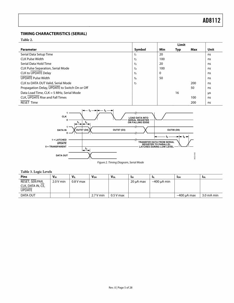
TIMING CHARACTERISTICS (SERIAL) Table 2. Limit Parameter Symbol Min Typ Max Unit Serial Data Setup Time t1 20 ns CLK Pulse Width t2 100 ns Serial Data Hold Time t3 20 ns CLK Pulse Separation, Serial Mode t4 100 ns CLK to UPDATE Delay t5 0 ns
UPDATE Pulse Width t6 50 ns
CLK to DATA OUT Valid, Serial Mode t7 200 ns Propagation Delay, UPDATE to Switch On or Off 50 ns
Data Load Time, CLK = 5 MHz, Serial Mode 16 μs CLK, UPDATE Rise and Fall Times 100 ns
RESET Time 200 ns
1
0
1
0
1 = LATCHED
0 = TRANSPARENT
DATA OUT
CLK
DATA IN
t2 t4
t1 t3
t7
t5 t6
OUT00 (D0)OUT07 (D3)OUT07 (D4)
TRANSFER DATA FROM SERIALREGISTER TO PARALLEL
LATCHES DURING LOW LEVEL
LOAD DATA INTOSERIAL REGISTERON FALLING EDGE
UPDATE
0652
3-00
2
Figure 2. Timing Diagram, Serial Mode
Table 3. Logic Levels Pins VIH VIL VOH VOL IIH IIL IOH IOL RESET, SER/PAR, CLK, DATA IN, CE, UPDATE
2.0 V min 0.8 V max 20 μA max −400 μA min
DATA OUT 2.7 V min 0.5 V max −400 μA max 3.0 mA min
AD8112
Rev. 0 | Page 6 of 28
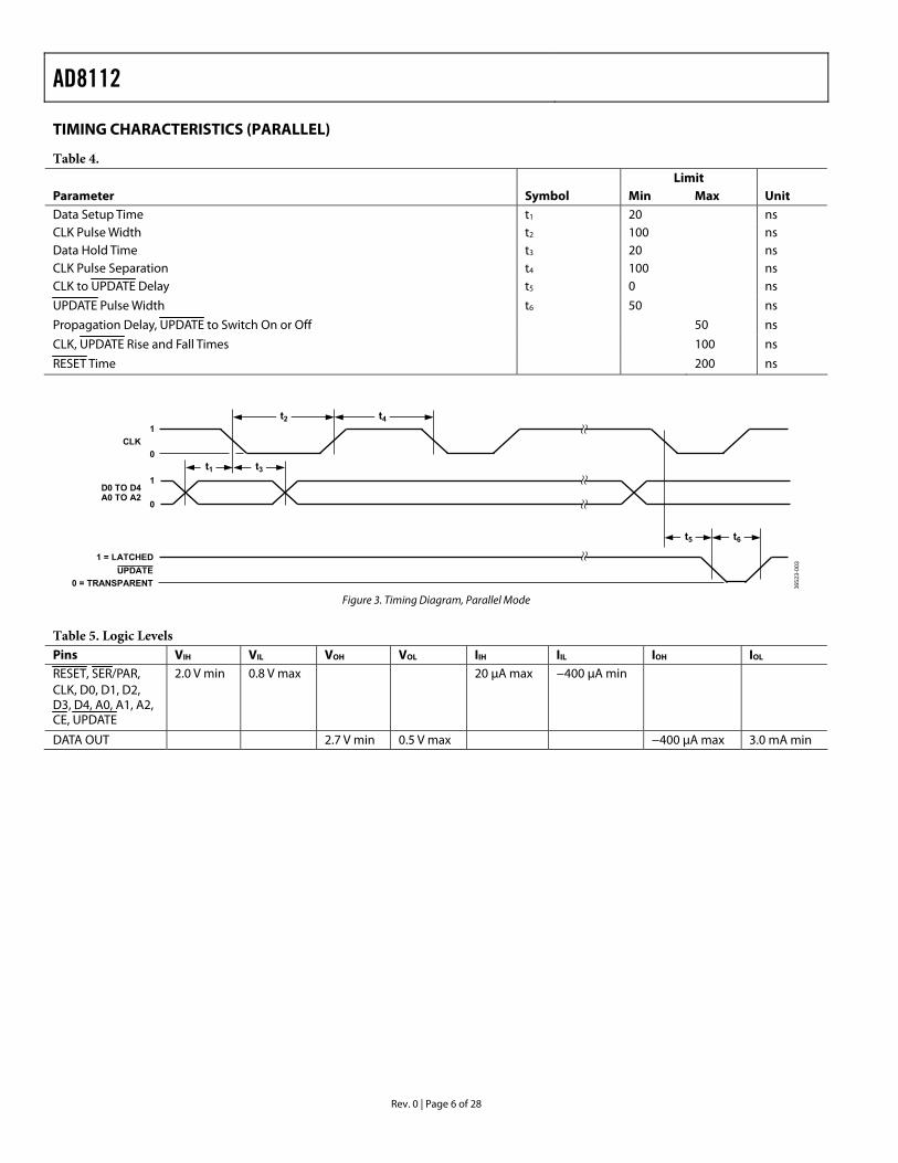
TIMING CHARACTERISTICS (PARALLEL)
Table 4. Limit Parameter Symbol Min Max Unit Data Setup Time t1 20 ns CLK Pulse Width t2 100 ns Data Hold Time t3 20 ns CLK Pulse Separation t4 100 ns CLK to UPDATE Delay t5 0 ns
UPDATE Pulse Width t6 50 ns
Propagation Delay, UPDATE to Switch On or Off 50 ns
CLK, UPDATE Rise and Fall Times 100 ns
RESET Time 200 ns
t5 t6
t4t2
t1 t3
1
0
1
0
1 = LATCHED
CLK
D0 TO D4A0 TO A2
0 = TRANSPARENTUPDATE
0652
3-00
3
Figure 3. Timing Diagram, Parallel Mode
Table 5. Logic Levels Pins VIH VIL VOH VOL IIH IIL IOH IOL RESET, SER/PAR, CLK, D0, D1, D2, D3, D4, A0, A1, A2, CE, UPDATE
2.0 V min 0.8 V max 20 μA max −400 μA min
DATA OUT 2.7 V min 0.5 V max −400 μA max 3.0 mA min
AD8112
Rev. 0 | Page 7 of 28
ABSOLUTE MAXIMUM RATINGS Table 6. Parameter Rating Analog Supply Voltage (AVCC to AVEE) 26.0 V Digital Supply Voltage (DVCC to DGND) 6 V Ground Potential Difference (AGND to DGND) ±0.5 V Internal Power Dissipation1 3.1 W Analog Input Voltage2 Maintain linear output Digital Input Voltage DVCC Output Voltage (Disabled Output) (AVCC − 1.5 V) to
(AVEE + 1.5 V) Output Short-Circuit Duration Momentary Storage Temperature Range −65°C to +125°C Lead Temperature (Soldering 10 sec) 300°C
1 Specification is for device in free air (TA = 25°C): 100-lead plastic LQFP (ST): θJA = 40°C/W.
2 To avoid differential input breakdown, ensure that one-half the output voltage (1/2 VOUT) and any input voltage is less than 10 V of the potential differential. See Output Voltage Swing specification for linear output range.
Stresses above those listed under Absolute Maximum Ratings may cause permanent damage to the device. This is a stress rating only; functional operation of the device at these or any other conditions above those indicated in the operational section of this specification is not implied. Exposure to absolute maximum rating conditions for extended periods may affect device reliability.
ESD CAUTION
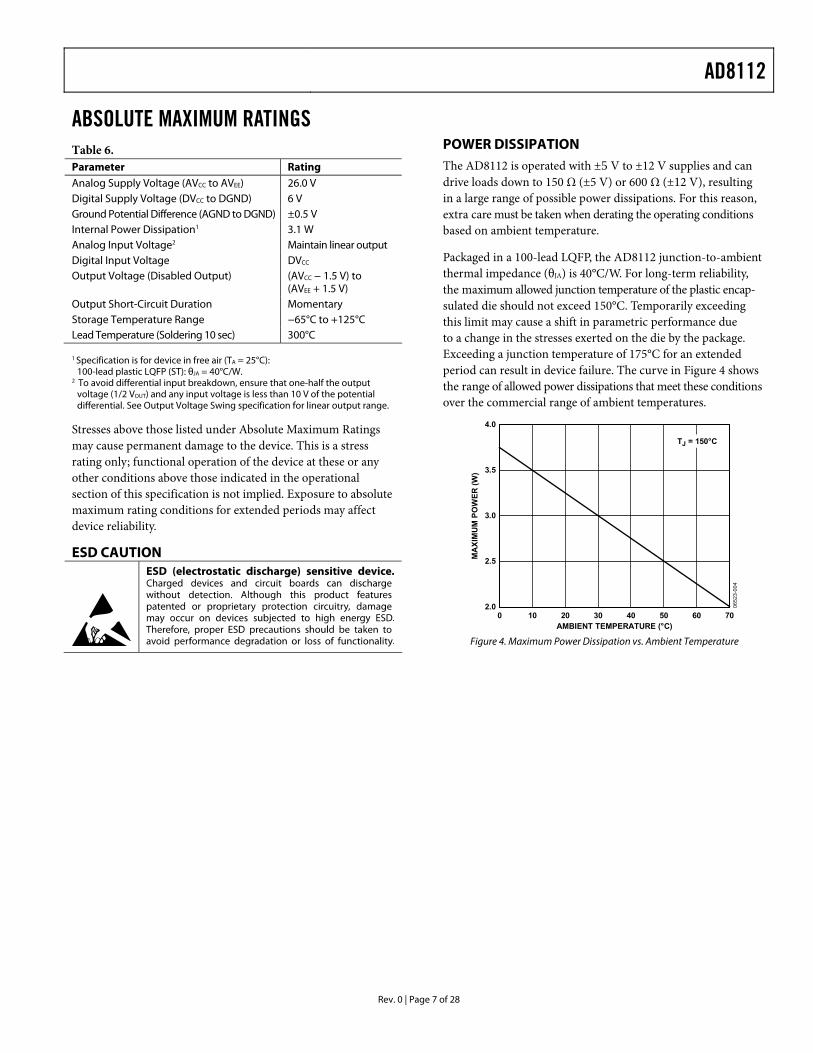
POWER DISSIPATION The AD8112 is operated with ±5 V to ±12 V supplies and can drive loads down to 150 Ω (±5 V) or 600 Ω (±12 V), resulting in a large range of possible power dissipations. For this reason, extra care must be taken when derating the operating conditions based on ambient temperature.
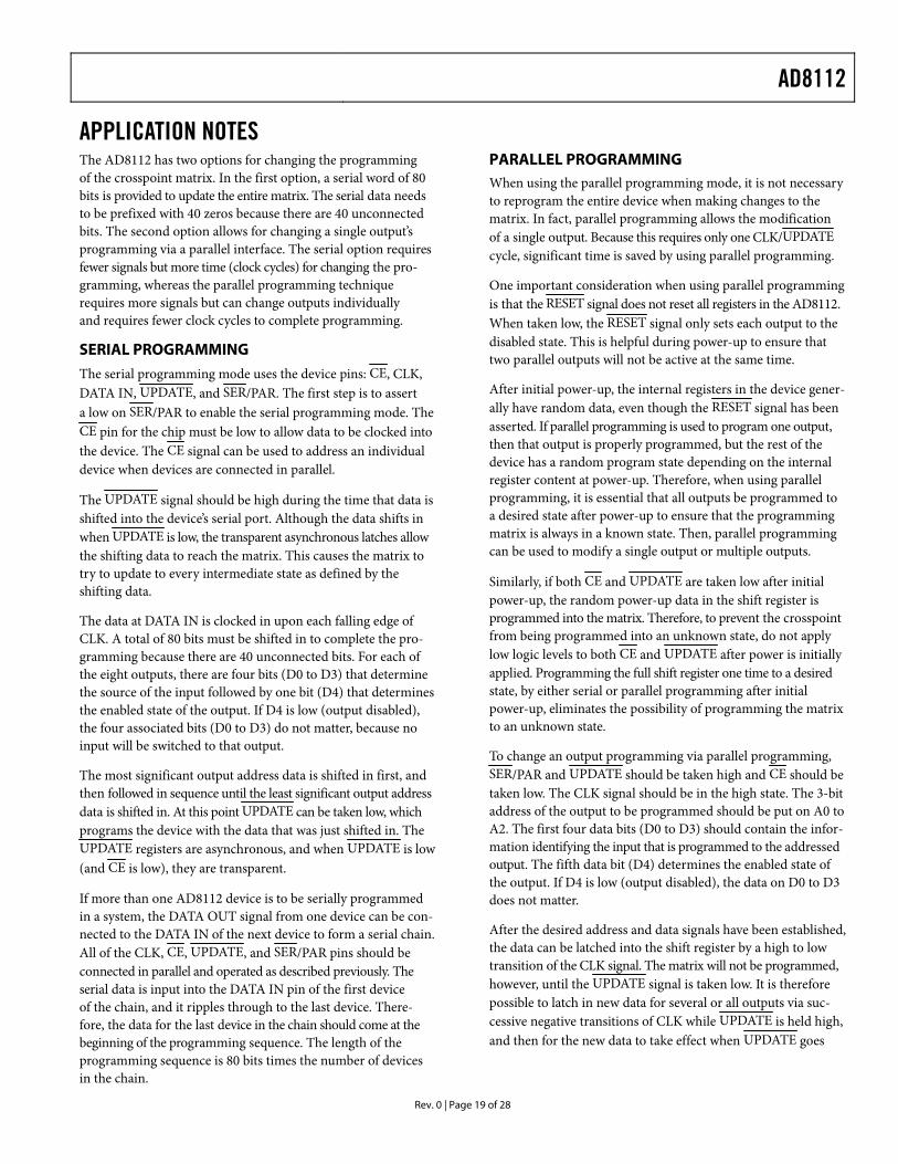
Packaged in a 100-lead LQFP, the AD8112 junction-to-ambient thermal impedance (θJA) is 40°C/W. For long-term reliability, the maximum allowed junction temperature of the plastic encap-sulated die should not exceed 150°C. Temporarily exceeding this limit may cause a shift in parametric performance due to a change in the stresses exerted on the die by the package. Exceeding a junction temperature of 175°C for an extended period can result in device failure. The curve in Figure 4 shows the range of allowed power dissipations that meet these conditions over the commercial range of ambient temperatures.
4.0
MA
XIM
UM
PO
WER
(W) 3.5
2.0
3.0
2.5
AMBIENT TEMPERATURE (°C)0 10 20 30 40 50 60 70
TJ = 150°C
0652
3-00
4
Figure 4. Maximum Power Dissipation vs. Ambient Temperature
AD8112
Rev. 0 | Page 8 of 28
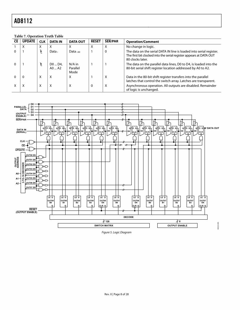
Table 7. Operation Truth Table CE UPDATE CLK DATA IN DATA OUT RESET SER/PAR Operation/Comment 1 X X X X X X No change in logic. 0 1 Data i Data i-80 1 0 The data on the serial DATA IN line is loaded into serial register.
The first bit clocked into the serial register appears at DATA OUT 80 clocks later.
0 1 D0 ... D4, A0 ... A2
N/A in Parallel Mode
1 1 The data on the parallel data lines, D0 to D4, is loaded into the 80-bit serial shift register location addressed by A0 to A2.
0 0 X X X 1 X Data in the 80-bit shift register transfers into the parallel latches that control the switch array. Latches are transparent.
X X X X X 0 X Asynchronous operation. All outputs are disabled. Remainder of logic is unchanged.
D
CLK
Q
3-TO
-16
DEC
OD
ER
A0
A1
A2
CLK
CE
UPDATE
8128
DATA IN(SERIAL)
(OUTPUTENABLE)SER/PAR
RESET(OUTPUT ENABLE)
OUT00 EN
DATA OUT
PARALLELDATA
D
CLK CLK CLK CLK
D1D2D3
CLK CLK CLK CLK CLK
OUT01 EN
OUT02 EN
OUT03 EN
OUT04 EN
OUT05 EN
OUT06 EN
OUT07 EN
DLE
QCLR
OUT07EN
OUTPUT ENABLESWITCH MATRIX
SD1
QD0
D0
SD1
QD0
SD1
QD0
SD1
QD0
SD1
QD0
SD1
QD0
SD1
QD0
SD1
QD0 CLK
SD1
QD0
D4
DECODE
DLE
QCLR
OUT00EN
DLEOUT00
B0Q
DLE
Q
OUT00B1
DLE
Q
OUT00B2
DLE
Q
OUT00B3
DLEOUT01
B0Q
DLE
QCLR
OUT06EN
DLEOUT07
B0Q
DLEOUT07
B1Q
DLEOUT07
B2Q
CLK
SD1
QD0
SD1
QD0
DLEOUT07
B3Q
SD1
QD0
OU
TPU
TA
DD
RES
S
Q D Q D Q D Q D Q D Q D Q D Q D Q D QD Q
0652
3-00
5
Figure 5. Logic Diagram
AD8112
Rev. 0 | Page 9 of 28
PIN CONFIGURATION AND FUNCTION DESCRIPTIONS
NC = NO CONNECT
RES
ETC
ED
ATA
OU
TC
LKD
ATA
INU
PDA
TESE
R/P
AR
NC
NC
NC
NC
NC
NC
NC
NC
NC
A0
A1
A2
DG
ND
D0
D1
D2
D3
D4
26A
V CC
27N
C28
AV E
E29
NC
30A
V CC
31N
C32
AV E
E33
NC
34A
V CC
35N
C36
AV E
E37
NC
38A
V CC
39O
UT0
7
2DGND3AGND4IN08
7AGND
6IN09
5AGND
1DVCC
8IN109AGND
10IN11
12IN1213AGND14IN1315AGND16IN1417AGND18IN1519AGND20AVEE21AVCC22AVCC23NC24AVEE25NC
11AGND
74 DGNDDVCC
73 AGND72 IN07
69 AGND
70 IN06
71 AGND
75
68 IN0567 AGND66 IN04
64 IN0363 AGND62 IN0261 AGND60 IN0159 AGND58 IN0057 AGND56 AVEE55 AVCC54 AVCC0053 OUT0052 AVEE00/0151 OUT01
65 AGND
40A
V EE0
6/07
41O
UT0
642
AV C
C05
/06
43O
UT0
544
AV E
E04/
0545
OU
T04
46A
V CC
03/0
447
OU
T03
48A
V EE0
2/03
49O
UT0
250
AV C
C01
/02
100
99 98 97 96 95 94 93 92 91 90 89 88 87 86 85 84 83 82 81 80 79 78 77 76
PIN 1
AD8112TOP VIEW
(Not to Scale)
0652
3-00
6
Figure 6. Pin Configuration
Table 8. Pin Function Descriptions Pin No. Mnemonic Description 58, 60, 62, 64, 66, 68, 70, 72, 4, 6, 8, 10, 12, 14, 16, 18
IN00 to IN151 Analog Inputs for Channel Numbers 00 through 15.
96 DATA IN Serial Data Input, TTL-compatible. 97 CLK Clock, TTL-compatible. Falling edge triggered. 98 DATA OUT Serial Data Output, TTL-compatible. 95 UPDATE Enable (Transparent) Low. Allows serial register to connect directly to switch
matrix. Data latched when high. 100 RESET Disable Outputs, Active Low.
99 CE Chip Enable, Enable Low. Must be low to clock in and latch data.
94 SER/PAR Serial Data/Parallel Data. When low, this pin selects serial data mode; when high, this pin selects parallel data mode, high. Must be connected.
53, 51, 49, 47, 45, 43, 41, 39 OUT00 to OUT071
Analog Outputs for Channel Numbers 00 Through 07.
3, 5, 7, 9, 11, 13, 15, 17, 19, 57, 59, 61, 63, 65, 67, 69, 71, 73
AGND Analog Ground for Inputs and Switch Matrix. Must be connected.
1, 75 DVCC 5 V for Digital Circuitry. 2, 74, 81 DGND Ground for Digital Circuitry. 20, 24, 28, 32, 36, 56 AVEE −5 V for Inputs and Switch Matrix.
AD8112
Rev. 0 | Page 10 of 28
Pin No. Mnemonic Description 21, 22, 26, 30, 34, 38, 55 AVCC 5 V for Inputs and Switch Matrix. 54 AVCCxx 5 V for Output Amplifier. This pin is shared by Channel Numbers xx and yy.
Must be connected. 50, 46, 42 AVCCxx/yy1 5 V for Output Amplifier. This pin is shared by Channel Numbers xx and yy.
Must be connected. 52, 48, 44, 40 AVEExx/yy1 −5 V for Output Amplifier. This pin is shared by Channel Numbers xx and yy.
Must be connected. 84 A0 Parallel Data Input, TTL-compatible (Output Select LSB). 83 A1 Parallel Data Input, TTL-compatible (Output Select). 82 A2 Parallel Data Input, TTL-compatible (Output Select). 80 D0 Parallel Data Input, TTL-compatible (Input Select LSB). 79 D1 Parallel Data Input, TTL-compatible (Input Select). 78 D2 Parallel Data Input, TTL-compatible (Input Select). 77 D3 Parallel Data Input, TTL-compatible (Input Select MSB). 76 D4 Parallel Data Input, TTL-compatible (Output Enable). 23, 25, 27, 29, 31, 33, 35, 37, 85 to 93 NC No Connect. 1 xx = Chanel numbers 00 through 15 for analog inputs; yy = channel numbers 00 through 07 for analog outputs.
AD8112
Rev. 0 | Page 11 of 28
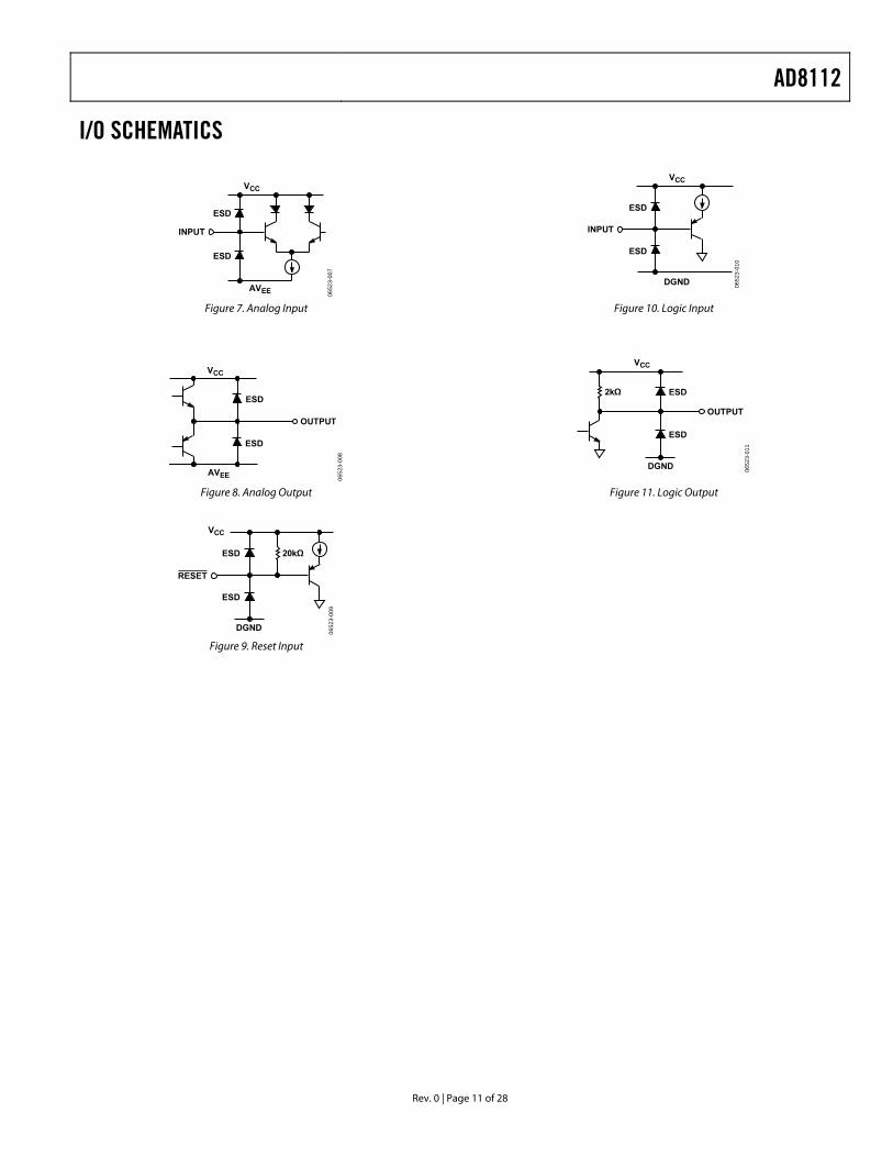
I/O SCHEMATICS
ESD
ESD
INPUT
VCC
AVEE 0652
3-00
7
Figure 7. Analog Input
ESD
ESD
OUTPUT
VCC
AVEE 0652
3-00
8
Figure 8. Analog Output
ESD
ESD
RESET
20kΩ
DGND
VCC
0652
3-00
9
Figure 9. Reset Input
ESD
ESD
INPUT
DGND
VCC
0652
3-01
0
Figure 10. Logic Input
ESD
ESD
OUTPUT
2kΩ
DGND
VCC
0652
3-01
1
Figure 11. Logic Output
AD8112
Rev. 0 | Page 12 of 28
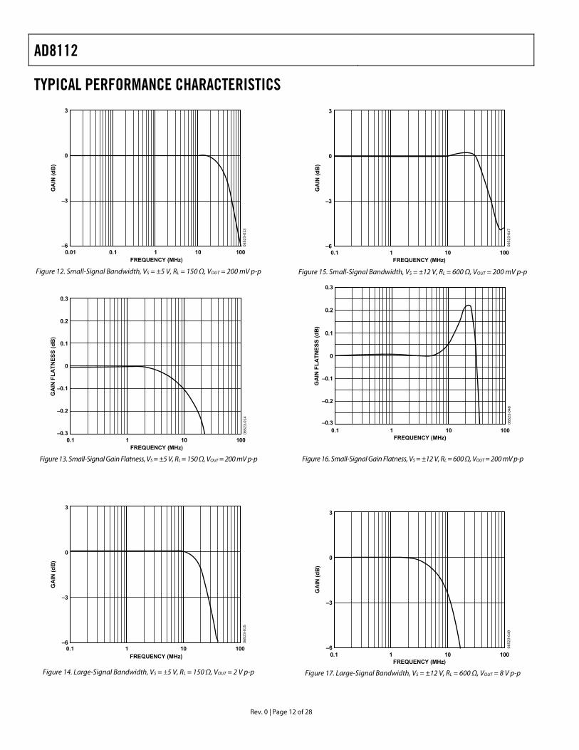
TYPICAL PERFORMANCE CHARACTERISTICS
FREQUENCY (MHz)
GA
IN (d
B)
–6
–3
0
3
0.01 0.1 1 10 10006
523-
013
Figure 12. Small-Signal Bandwidth, VS = ±5 V, RL = 150 Ω, VOUT = 200 mV p-p
FREQUENCY (MHz)
GA
IN F
LATN
ESS
(dB
)
–0.3
–0.2
–0.1
0.3
0
0.1
0.2
0.1 1 10 100
0652
3-01
4
Figure 13. Small-Signal Gain Flatness, VS = ±5 V, RL = 150 Ω, VOUT = 200 mV p-p
FREQUENCY (MHz)
GA
IN (d
B)
–6
–3
0
3
0.1 1 10 100
0652
3-01
5
Figure 14. Large-Signal Bandwidth, VS = ±5 V, RL = 150 Ω, VOUT = 2 V p-p
FREQUENCY (MHz)
GA
IN (d
B)
–6
–3
0
3
0.1 100101
0652
3-04
7
Figure 15. Small-Signal Bandwidth, VS = ±12 V, RL = 600 Ω, VOUT = 200 mV p-p
FREQUENCY (MHz)
GA
IN F
LATN
ESS
(dB
)
–0.3
0
–0.2
–0.1
0.1
0.2
0.3
0.1 100101
0652
3-04
8
Figure 16. Small-Signal Gain Flatness, VS = ±12 V, RL = 600 Ω, VOUT = 200 mV p-p
FREQUENCY (MHz)
GA
IN (d
B)
–6
–3
0
3
0.1 100101
0652
3-04
9
Figure 17. Large-Signal Bandwidth, VS = ±12 V, RL = 600 Ω, VOUT = 8 V p-p
AD8112
Rev. 0 | Page 13 of 28
FREQUENCY (MHz)
GA
IN F
LATN
ESS
(dB
)
–0.3
–0.2
–0.1
0.3
0
0.1
0.2
0.1 1 10 100
0652
3-01
6
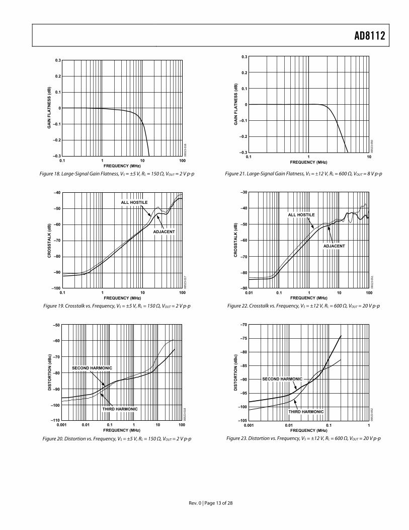
Figure 18. Large-Signal Gain Flatness, VS = ±5 V, RL = 150 Ω, VOUT = 2 V p-p
FREQUENCY (MHz)
CR
OSS
TALK
(dB
)
–100
–90
–80
–70
–60
–50
–40
0652
3-01
7
10.1 10 100
ADJACENT
ALL HOSTILE
Figure 19. Crosstalk vs. Frequency, VS = ±5 V, RL = 150 Ω, VOUT = 2 V p-p
FREQUENCY (MHz)
DIS
TOR
TIO
N (d
Bc)
–110
–100
–90
–80
–70
–60
–50
SECOND HARMONIC
THIRD HARMONIC
0.001 0.01 0.1 1 10 100
0652
3-01
8
Figure 20. Distortion vs. Frequency, VS = ±5 V, RL = 150 Ω, VOUT = 2 V p-p
GA
IN F
LATN
ESS
(dB
)
FREQUENCY (MHz)
–0.3
0
0.1 101
–0.2
–0.1
0.1
0.2
0.3
0652
3-05
0
Figure 21. Large-Signal Gain Flatness, VS = ±12 V, RL = 600 Ω, VOUT = 8 V p-p
FREQUENCY (MHz)
CR
OSS
TALK
(dB
)
–90
–80
–70
–60
–50
–40
–30
ALL HOSTILE
ADJACENT
0.01 0.1 1 10 100
0652
3-05
1
Figure 22. Crosstalk vs. Frequency, VS = ±12 V, RL = 600 Ω, VOUT = 20 V p-p
DIS
TOR
TIO
N (d
Bc)
–105
–100
–80
FREQUENCY (MHz)
–70
–75
–85
–90
–95
THIRD HARMONIC
SECOND HARMONIC
0.001 0.01 0.1 1
0652
3-05
2
Figure 23. Distortion vs. Frequency, VS = ±12 V, RL = 600 Ω, VOUT = 20 V p-p
AD8112
Rev. 0 | Page 14 of 28
CA
PAC
ITIV
E LO
AD
(pF)
300
250
200
150
100
50
0
SERIES RESISTANCE (Ω)
VS = ±12VRL = 600Ω
VS = ±5VRL = 150Ω
0 5 10 15 20 25 30 3506
523-
019
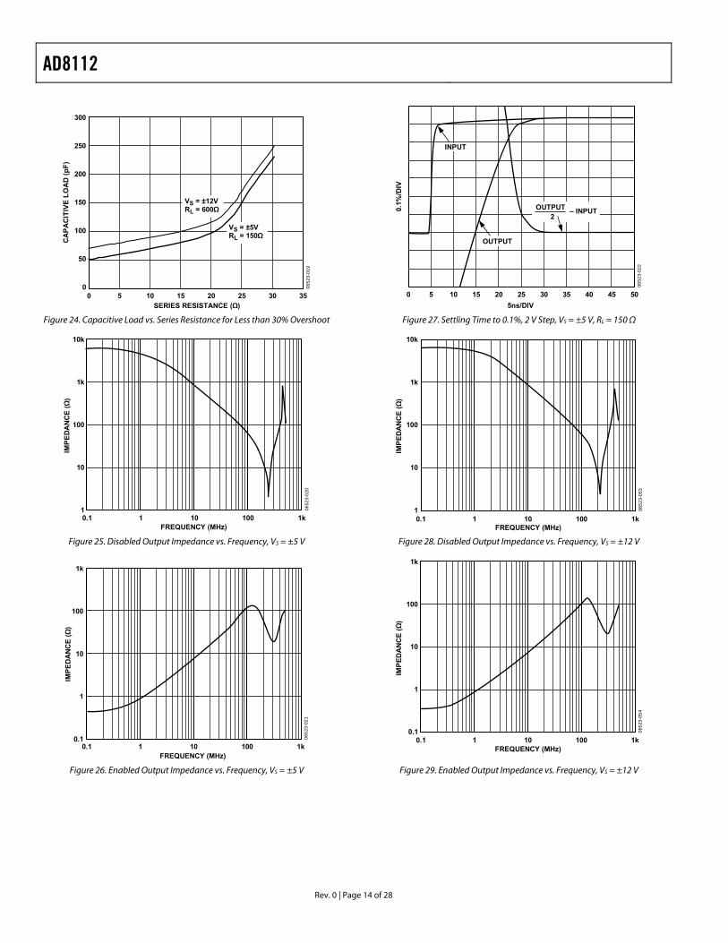
Figure 24. Capacitive Load vs. Series Resistance for Less than 30% Overshoot
IMPE
DA
NC
E (Ω
)
1
100
1k
10k
10
FREQUENCY (MHz)0.1 1 10 100 1k
0652
3-02
0
Figure 25. Disabled Output Impedance vs. Frequency, VS = ±5 V
IMPE
DA
NC
E (Ω
)
1
100
1k
10
FREQUENCY (MHz)
0.10.1 1 10 100 1k
0652
3-02
1
Figure 26. Enabled Output Impedance vs. Frequency, VS = ±5 V
INPUT
OUTPUT
5ns/DIV
0.1%
/DIV
OUTPUT – INPUT2
0 5 10 15 20 25 30 35 40 45 50
0652
3-02
2
Figure 27. Settling Time to 0.1%, 2 V Step, VS = ±5 V, RL = 150 Ω
IMPE
DA
NC
E (Ω
)
1
100
1k
10k
10
FREQUENCY (MHz)100 1k0.1 1 10
0652
3-05
3
Figure 28. Disabled Output Impedance vs. Frequency, VS = ±12 V
1
100
1k
10
FREQUENCY (MHz)
0.1
IMPE
DA
NC
E (Ω
)
0.1 1 10 100 1k
0652
3-05
4
Figure 29. Enabled Output Impedance vs. Frequency, VS = ±12 V
AD8112
Rev. 0 | Page 15 of 28
FREQUENCY (MHz)
PSR
R (d
B)
–90
–80
–70
–60
–50
–40
–30
–20
–10
0
+PSRR
–PSRR
0.01 0.1 1 10
0652
3-02
3
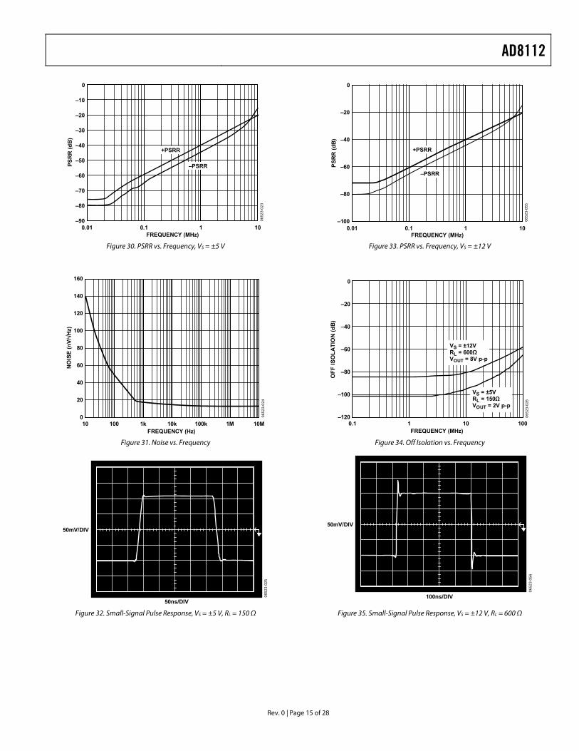
Figure 30. PSRR vs. Frequency, VS = ±5 V
NO
ISE
(nV/
Hz)
FREQUENCY (Hz)
0
20
40
60
80
100
120
140
160
10 100 1k 10k 100k 1M 10M
0652
3-02
4
Figure 31. Noise vs. Frequency
50ns/DIV
50mV/DIV
0652
3-02
5
Figure 32. Small-Signal Pulse Response, VS = ±5 V, RL = 150 Ω
FREQUENCY (MHz)
PSR
R (d
B)
–100
–80
–60
–40
–20
0
+PSRR
–PSRR
1010.10.01
0652
3-05
5
Figure 33. PSRR vs. Frequency, VS = ±12 V
FREQUENCY (MHz)
OFF
ISO
LATI
ON
(dB
)
–20
0
–40
–60
–80
–100
–1200.1 1 10 100
VS = ±12VRL = 600ΩVOUT = 8V p-p
VS = ±5VRL = 150ΩVOUT = 2V p-p
0652
3-02
6
Figure 34. Off Isolation vs. Frequency
100ns/DIV
50mV/DIV06
523-
056
Figure 35. Small-Signal Pulse Response, VS = ±12 V, RL = 600 Ω
AD8112
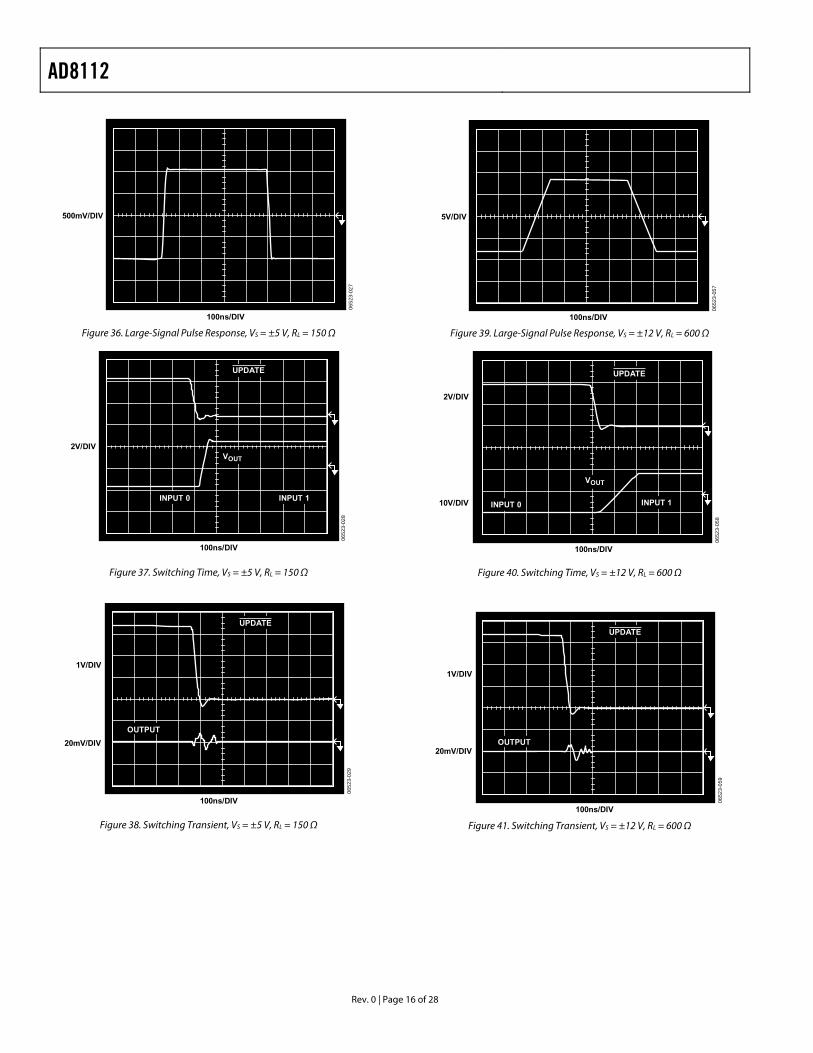
Rev. 0 | Page 16 of 28
100ns/DIV
500mV/DIV
0652
3-02
7
Figure 36. Large-Signal Pulse Response, VS = ±5 V, RL = 150 Ω
100ns/DIV
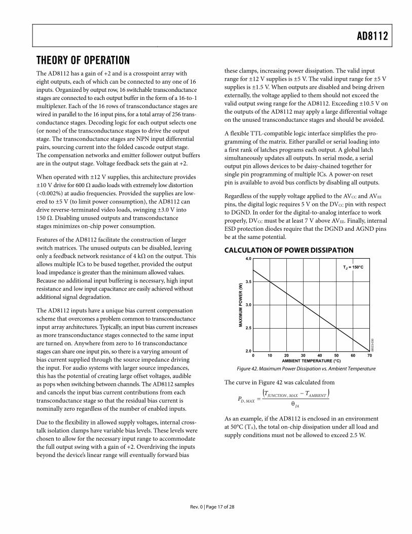
2V/DIV
UPDATE
VOUT
INPUT 0 INPUT 1
0652
3-02
8
Figure 37. Switching Time, VS = ±5 V, RL = 150 Ω
100ns/DIV
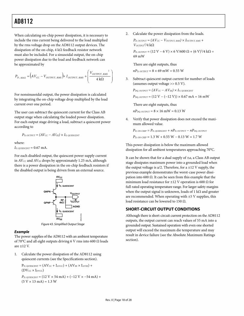
1V/DIV
20mV/DIVOUTPUT
UPDATE
0652
3-02
9
Figure 38. Switching Transient, VS = ±5 V, RL = 150 Ω
100ns/DIV
5V/DIV
0652
3-05
7
Figure 39. Large-Signal Pulse Response, VS = ±12 V, RL = 600 Ω
10V/DIV
100ns/DIV
2V/DIV
UPDATE
VOUT
INPUT 1INPUT 0
0652
3-05
8
Figure 40. Switching Time, VS = ±12 V, RL = 600 Ω
100ns/DIV
1V/DIV
20mV/DIVOUTPUT
UPDATE
0652
3-05
9
Figure 41. Switching Transient, VS = ±12 V, RL = 600 Ω
AD8112
Rev. 0 | Page 17 of 28
THEORY OF OPERATION The AD8112 has a gain of +2 and is a crosspoint array with eight outputs, each of which can be connected to any one of 16 inputs. Organized by output row, 16 switchable transconductance stages are connected to each output buffer in the form of a 16-to-1 multiplexer. Each of the 16 rows of transconductance stages are wired in parallel to the 16 input pins, for a total array of 256 trans-conductance stages. Decoding logic for each output selects one (or none) of the transconductance stages to drive the output stage. The transconductance stages are NPN input differential pairs, sourcing current into the folded cascode output stage. The compensation networks and emitter follower output buffers are in the output stage. Voltage feedback sets the gain at +2.
When operated with ±12 V supplies, this architecture provides ±10 V drive for 600 Ω audio loads with extremely low distortion (<0.002%) at audio frequencies. Provided the supplies are low-ered to ±5 V (to limit power consumption), the AD8112 can drive reverse-terminated video loads, swinging ±3.0 V into 150 Ω. Disabling unused outputs and transconductance stages minimizes on-chip power consumption.
Features of the AD8112 facilitate the construction of larger switch matrices. The unused outputs can be disabled, leaving only a feedback network resistance of 4 kΩ on the output. This allows multiple ICs to be bused together, provided the output load impedance is greater than the minimum allowed values. Because no additional input buffering is necessary, high input resistance and low input capacitance are easily achieved without additional signal degradation.
The AD8112 inputs have a unique bias current compensation scheme that overcomes a problem common to transconductance input array architectures. Typically, an input bias current increases as more transconductance stages connected to the same input are turned on. Anywhere from zero to 16 transconductance stages can share one input pin, so there is a varying amount of bias current supplied through the source impedance driving the input. For audio systems with larger source impedances, this has the potential of creating large offset voltages, audible as pops when switching between channels. The AD8112 samples and cancels the input bias current contributions from each transconductance stage so that the residual bias current is nominally zero regardless of the number of enabled inputs.
Due to the flexibility in allowed supply voltages, internal cross-talk isolation clamps have variable bias levels. These levels were chosen to allow for the necessary input range to accommodate the full output swing with a gain of +2. Overdriving the inputs beyond the device’s linear range will eventually forward bias
these clamps, increasing power dissipation. The valid input range for ±12 V supplies is ±5 V. The valid input range for ±5 V supplies is ±1.5 V. When outputs are disabled and being driven externally, the voltage applied to them should not exceed the valid output swing range for the AD8112. Exceeding ±10.5 V on the outputs of the AD8112 may apply a large differential voltage on the unused transconductance stages and should be avoided.
A flexible TTL-compatible logic interface simplifies the pro-gramming of the matrix. Either parallel or serial loading into a first rank of latches programs each output. A global latch simultaneously updates all outputs. In serial mode, a serial output pin allows devices to be daisy-chained together for single pin programming of multiple ICs. A power-on reset pin is available to avoid bus conflicts by disabling all outputs.
Regardless of the supply voltage applied to the AVCC and AVEE pins, the digital logic requires 5 V on the DVCC pin with respect to DGND. In order for the digital-to-analog interface to work properly, DVCC must be at least 7 V above AVEE. Finally, internal ESD protection diodes require that the DGND and AGND pins be at the same potential.
CALCULATION OF POWER DISSIPATION 4.0
MA
XIM
UM
PO
WER
(W) 3.5
2.0
3.0
2.5
AMBIENT TEMPERATURE (°C)0 10 20 30 40 50 60 70
TJ = 150°C
0652
3-03
0
Figure 42. Maximum Power Dissipation vs. Ambient Temperature
The curve in Figure 42 was calculated from
( )JA
AMBIENTMAXJUNCTIONMAXD
TTP
θ
−= ,
,
As an example, if the AD8112 is enclosed in an environment at 50°C (TA), the total on-chip dissipation under all load and supply conditions must not be allowed to exceed 2.5 W.
AD8112
Rev. 0 | Page 18 of 28
When calculating on-chip power dissipation, it is necessary to include the rms current being delivered to the load multiplied by the rms voltage drop on the AD8112 output devices. The dissipation of the on-chip, 4 kΩ feedback resistor network must also be included. For a sinusoidal output, the on-chip power dissipation due to the load and feedback network can be approximated by
( )⎟⎟⎟
⎠
⎞
⎜⎜⎜
⎝
⎛
Ω+×−=
k4
2
,,,,
RMSOUTPUTRMSOUTPUTRMSOUTPUTCCMAXD
VIVAVP
For nonsinusoidal output, the power dissipation is calculated by integrating the on-chip voltage drop multiplied by the load current over one period.
The user can subtract the quiescent current for the Class AB output stage when calculating the loaded power dissipation. For each output stage driving a load, subtract a quiescent power according to
PD, OUTPUT = (AVCC − AVEE) × IO, QUIESCENT
where: IO, QUIESCENT = 0.67 mA.
For each disabled output, the quiescent power supply current in AVCC and AVEE drops by approximately 1.25 mA, although there is a power dissipation in the on-chip feedback resistors if the disabled output is being driven from an external source.
AGNDQPNP
QNPN
AVCC
IO, QUIESCENT
VOUTPUT
IOUTPUTRF
4kΩ
IO, QUIESCENT
AVEE 0652
3-03
1
Figure 43. Simplified Output Stage
Example The power supplies of the AD8112 with an ambient temperature of 70°C and all eight outputs driving 6 V rms into 600 Ω loads are ±12 V.
1. Calculate the power dissipation of the AD8112 using quiescent currents (see the Specifications section).
PD, QUIESCENT = (AVCC + IAVCC) + (AVEE × IAVEE) + (DVCC × IDVCC)
PD, QUIESCENT = (12 V × 54 mA) + (−12 V × −54 mA) + (5 V × 13 mA) = 1.3 W
2. Calculate the power dissipation from the loads.
PD, OUTPUT = (AVCC − VOUTPUT, RMS) × IOUTPUT, RMS + VOUTPUT
2/4 kΩ
PD, OUTPUT = (12 V − 6 V) × 6 V/600 Ω + (6 V)2/4 kΩ = 69 mW
There are eight outputs, thus
nPD, OUTPUT = 8 × 69 mW = 0.55 W
3. Subtract quiescent output current for number of loads (assumes output voltage >> 0.5 V).
PDQ, OUTPUT = (AVCC − AVEE) × IO, QUIESCENT
PDQ, OUTPUT = (12 V − (−12 V)) × 0.67 mA = 16 mW
There are eight outputs, thus
nPDQ, OUTPUT = 8 × 16 mW = 0.13 W
4. Verify that power dissipation does not exceed the maxi-mum allowed value.
PD, ON-CHIP = PD, QUIESCENT + nPD, OUTPUT − nPDQ, OUTPUT
PD, ON-CHIP = 1.3 W + 0.55 W − 0.13 W = 1.7 W
This power dissipation is below the maximum allowed dissipation for all ambient temperatures approaching 70°C.
It can be shown that for a dual supply of ±a, a Class AB output stage dissipates maximum power into a grounded load when the output voltage is a/2. Therefore, for a ±12 V supply, the previous example demonstrates the worst-case power dissi-pation into 600 Ω. It can be seen from this example that the minimum load resistance for ±12 V operation is 600 Ω for full rated operating temperature range. For larger safety margins when the output signal is unknown, loads of 1 kΩ and greater are recommended. When operating with ±5 V supplies, this load resistance can be lowered to 150 Ω.
SHORT-CIRCUIT OUTPUT CONDITIONS Although there is short-circuit current protection on the AD8112 outputs, the output current can reach values of 55 mA into a grounded output. Sustained operation with even one shorted output will exceed the maximum die temperature and may result in device failure (see the Absolute Maximum Ratings section).
AD8112
Rev. 0 | Page 19 of 28
APPLICATION NOTESThe AD8112 has two options for changing the programming of the crosspoint matrix. In the first option, a serial word of 80 bits is provided to update the entire matrix. The serial data needs to be prefixed with 40 zeros because there are 40 unconnected bits. The second option allows for changing a single output’s programming via a parallel interface. The serial option requires fewer signals but more time (clock cycles) for changing the pro-gramming, whereas the parallel programming technique requires more signals but can change outputs individually and requires fewer clock cycles to complete programming.
SERIAL PROGRAMMING
The serial programming mode uses the device pins: CE, CLK, DATA IN, UPDATE, and SER/PAR. The first step is to assert a low on SER/PAR to enable the serial programming mode. The CE pin for the chip must be low to allow data to be clocked into the device. The CE signal can be used to address an individual device when devices are connected in parallel.
The UPDATE signal should be high during the time that data is shifted into the device’s serial port. Although the data shifts in when UPDATE is low, the transparent asynchronous latches allow the shifting data to reach the matrix. This causes the matrix to try to update to every intermediate state as defined by the shifting data.
The data at DATA IN is clocked in upon each falling edge of CLK. A total of 80 bits must be shifted in to complete the pro-gramming because there are 40 unconnected bits. For each of the eight outputs, there are four bits (D0 to D3) that determine the source of the input followed by one bit (D4) that determines the enabled state of the output. If D4 is low (output disabled), the four associated bits (D0 to D3) do not matter, because no input will be switched to that output.
The most significant output address data is shifted in first, and then followed in sequence until the least significant output address data is shifted in. At this point UPDATE can be taken low, which programs the device with the data that was just shifted in. The UPDATE registers are asynchronous, and when UPDATE is low (and CE is low), they are transparent.
If more than one AD8112 device is to be serially programmed in a system, the DATA OUT signal from one device can be con-nected to the DATA IN of the next device to form a serial chain. All of the CLK, CE, UPDATE, and SER/PAR pins should be connected in parallel and operated as described previously. The serial data is input into the DATA IN pin of the first device of the chain, and it ripples through to the last device. There-fore, the data for the last device in the chain should come at the beginning of the programming sequence. The length of the programming sequence is 80 bits times the number of devices in the chain.
PARALLEL PROGRAMMING When using the parallel programming mode, it is not necessary to reprogram the entire device when making changes to the matrix. In fact, parallel programming allows the modification of a single output. Because this requires only one CLK/UPDATE cycle, significant time is saved by using parallel programming.
One important consideration when using parallel programming is that the RESET signal does not reset all registers in the AD8112. When taken low, the RESET signal only sets each output to the disabled state. This is helpful during power-up to ensure that two parallel outputs will not be active at the same time.
After initial power-up, the internal registers in the device gener-ally have random data, even though the RESET signal has been asserted. If parallel programming is used to program one output, then that output is properly programmed, but the rest of the device has a random program state depending on the internal register content at power-up. Therefore, when using parallel programming, it is essential that all outputs be programmed to a desired state after power-up to ensure that the programming matrix is always in a known state. Then, parallel programming can be used to modify a single output or multiple outputs.
Similarly, if both CE and UPDATE are taken low after initial power-up, the random power-up data in the shift register is programmed into the matrix. Therefore, to prevent the crosspoint from being programmed into an unknown state, do not apply low logic levels to both CE and UPDATE after power is initially applied. Programming the full shift register one time to a desired state, by either serial or parallel programming after initial power-up, eliminates the possibility of programming the matrix to an unknown state.
To change an output programming via parallel programming, SER/PAR and UPDATE should be taken high and CE should be taken low. The CLK signal should be in the high state. The 3-bit address of the output to be programmed should be put on A0 to A2. The first four data bits (D0 to D3) should contain the infor-mation identifying the input that is programmed to the addressed output. The fifth data bit (D4) determines the enabled state of the output. If D4 is low (output disabled), the data on D0 to D3 does not matter.
After the desired address and data signals have been established, the data can be latched into the shift register by a high to low transition of the CLK signal. The matrix will not be programmed, however, until the UPDATE signal is taken low. It is therefore possible to latch in new data for several or all outputs via suc-cessive negative transitions of CLK while UPDATE is held high, and then for the new data to take effect when UPDATE goes
AD8112
Rev. 0 | Page 20 of 28
low. This technique should be used when programming the device for the first time after power-up when using parallel programming.
POWER-ON RESET When powering up the AD8112, it is usually desirable to have the outputs in the disabled state. The RESET pin, when taken low, causes all outputs to be in the disabled state. However, the RESET signal does not reset all registers in the AD8112. This is important when operating in the parallel programming mode. (Please refer to the Parallel Programming section for information about programming internal registers after power-up.) Serial programming updates the entire matrix, therefore no special considerations apply.
Because the data in the shift register is random after power-up, it should not be used to program the matrix; otherwise the matrix can enter an unknown state. To prevent this, do not apply logic low signals to both CE and UPDATE immediately after power-up. The shift register should first be loaded with the desired data, and then UPDATE can be taken low to program the device.
The RESET pin has a 20 kΩ pull-up resistor to DVCC that can be used to create a simple power-up reset circuit. A capacitor from RESET to ground holds RESET low until the device stabilizes. The low condition causes all the outputs to be disabled. The capacitor then charges through the pull-up resistor to the high state, thus allowing full programming capability of the device.
SPECIFYING AUDIO LEVELS Several methods are used to specify audio levels. A level is actually a power measurement, which requires not just a voltage meas-urement, but also a reference impedance. Traditionally both 150 Ω and 600 Ω have been used as references for audio level measurements.
The typical reference power level is 1 mW. Power levels that are measured relative to this reference level are given the designation dBm. However, it is necessary to be sure of the reference imped-ance used for such measurements. This can be either explicit (for example, 0 dBm (600 Ω)) or implicit (if there is an agree-ment on what the reference impedance is).
Because modern voltmeters have high input impedances, meas-urements can be made that do not terminate the signal. Therefore, it is not proper to consider this type of measurement a dBm, or power measurement. However, a measurement scale that is designated dBu is used to measure unterminated voltages. This scale has a voltage reference for 0 dBu that is the same as the voltage required to produce 0 dBm (600 Ω).
Because P = V2/R, the voltage required to create 1 mW into 600 Ω is 0.775 V rms. This is the voltage reference (0 dB) used for dBu measurements without regard to the impedance.
The AD8112 operates as a voltage-in/voltage-out device. Therefore, all parameters are specified in volts, but users can convert the values to other power units or decibel-type measurements as required by a particular application.
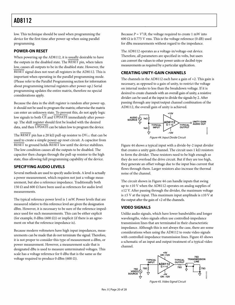
CREATING UNITY-GAIN CHANNELS The channels in the AD8112 each have a gain of +2. This gain is necessary, as opposed to a gain of unity, to restrict the voltage on internal nodes to less than the breakdown voltage. If it is desired to create channels with an overall gain of unity, a resistive divider can be used at the input to divide the signals by 2. After passing through any input/output channel combination of the AD8112, the overall gain of unity is achieved.
1kΩ
1kΩ
+12V
–12V
UNITY GAINAUDIO OUTTYPICAL
OUTPUTTYPICAL
INPUT
AUDIOSOURCE
AD8112G = +2
0652
3-03
2
Figure 44. Input Divide Circuit
Figure 44 shows a typical input with a divide-by-2 input divider that creates a unity gain channel. The circuit uses 1 kΩ resistors to form the divider. These resistors need to be high enough so they do not overload the drive circuit. But if they are too high, they generate an offset voltage due to the input bias current that flows through them. Larger resistors also increase the thermal noise of the channel.
The circuit shown in Figure 44 can handle inputs that swing up to ±10 V when the AD8112 operates on analog supplies of ±12 V. After passing through the divider, the maximum voltage is ±5 V at the input. This maximum input amplitude is ±10 V at the output after the gain of +2 of the channels.
VIDEO SIGNALS Unlike audio signals, which have lower bandwidths and longer wavelengths, video signals often use controlled-impedance transmission lines that are terminated in their characteristic impedance. Although this is not always the case, there are some considerations when using the AD8112 to route video signals with controlled-impedance transmission lines. Figure 45 shows a schematic of an input and output treatment of a typical video channel.
75Ω 75Ω 75Ω
75ΩTRANSMISSION
LINETYPICALOUTPUT
+5VOR +12V
AD8112G = +2
–5VOR –12V
TYPICALINPUT
75ΩVIDEO
SOURCE
0652
3-03
3
Figure 45. Video Signal Circuit
AD8112
Rev. 0 | Page 21 of 28
Video signals usually use 75 Ω transmission lines that need to be terminated with this value of resistance at each end. When such a source is delivered to one of the AD8112 inputs, the high input impedance does not properly terminate these signals. Therefore, the line should be terminated with a 75 Ω shunt resistor to ground. Because video signals are limited in their peak-to-peak amplitude, there is no need to attenuate video signals before they pass through the AD8112.
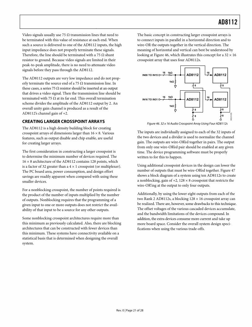
The basic concept in constructing larger crosspoint arrays is to connect inputs in parallel in a horizontal direction and to wire-OR the outputs together in the vertical direction. The meaning of horizontal and vertical can best be understood by looking at Figure 46, which illustrates this concept for a 32 × 16 crosspoint array that uses four AD8112s.
1kΩ
AD8112
AD8112
IN00 TO IN15
IN16 TO IN31
AD8112
AD81121kΩ
1kΩ
1kΩ
16
1616
16
8
8
8
8
8
8
0652
3-03
5
The AD8112 outputs are very low impedance and do not prop-erly terminate the source end of a 75 Ω transmission line. In these cases, a series 75 Ω resistor should be inserted at an output that drives a video signal. Then the transmission line should be terminated with 75 Ω at its far end. This overall termination scheme divides the amplitude of the AD8112 output by 2. An overall unity gain channel is produced as a result of the AD8112’s channel gain of +2.
CREATING LARGER CROSSPOINT ARRAYS Figure 46. 32 x 16 Audio Crosspoint Array Using Four AD8112s
The AD8112 is a high density building block for creating crosspoint arrays of dimensions larger than 16 × 8. Various features, such as output disable and chip enable, are useful for creating larger arrays.
The inputs are individually assigned to each of the 32 inputs of the two devices and a divider is used to normalize the channel gain. The outputs are wire-OR’ed together in pairs. The output from only one wire-OR’ed pair should be enabled at any given time. The device programming software must be properly written to for this to happen.
The first consideration in constructing a larger crosspoint is to determine the minimum number of devices required. The 16 × 8 architecture of the AD8112 contains 128 points, which is a factor of 32 greater than a 4 × 1 crosspoint (or multiplexer). The PC board area, power consumption, and design effort savings are readily apparent when compared with using these smaller devices.
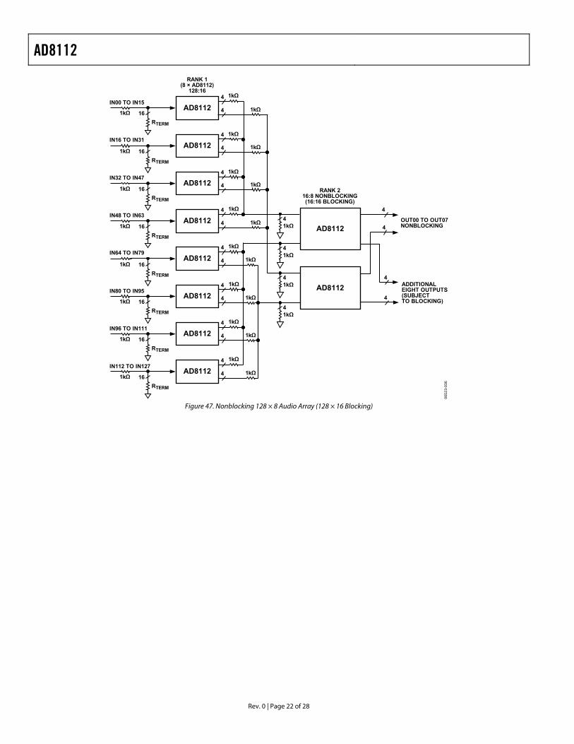
Using additional crosspoint devices in the design can lower the number of outputs that must be wire-OR’ed together. Figure 47 shows a block diagram of a system using ten AD8112s to create a nonblocking, gain of +2, 128 × 8 crosspoint that restricts the wire-OR’ing at the output to only four outputs.
For a nonblocking crosspoint, the number of points required is the product of the number of inputs multiplied by the number of outputs. Nonblocking requires that the programming of a given input to one or more outputs does not restrict the avail-ability of that input to be a source for any other outputs.
Additionally, by using the lower eight outputs from each of the two Rank 2 AD8112s, a blocking 128 × 16 crosspoint array can be realized. There are, however, some drawbacks to this technique. The offset voltages of the various cascaded devices accumulate, and the bandwidth limitations of the devices compound. In addition, the extra devices consume more current and take up more board space. Consider the overall system design speci-fications when using the various trade-offs.
Some nonblocking crosspoint architectures require more than this minimum as previously calculated. Also, there are blocking architectures that can be constructed with fewer devices than this minimum. These systems have connectivity available on a statistical basis that is determined when designing the overall system.
AD8112
Rev. 0 | Page 22 of 28
4
4
4
4
4
4
4
4
4
4
4
4
4
4
4
4
4
16RTERM
IN00 TO IN15
IN16 TO IN31
IN32 TO IN47
IN64 TO IN79
IN80 TO IN95
IN96 TO IN111
IN112 TO IN127
4
4
4
4
AD8112
AD8112
AD8112
AD8112
AD8112
AD8112
AD8112
AD8112
1kΩ
16RTERM
1kΩ
16RTERM
1kΩ
16RTERM
1kΩ
16RTERM
1kΩ
16RTERM
1kΩ
16RTERM
1kΩ
16RTERM
1kΩ
IN48 TO IN63
1kΩ
1kΩ
1kΩ
1kΩ
1kΩ
1kΩ
1kΩ
1kΩ
41kΩ
41kΩ
41kΩ
1kΩ
1kΩ
1kΩ
1kΩ
1kΩ
1kΩ
1kΩ
1kΩ
1kΩ
AD8112
AD8112
RANK 216:8 NONBLOCKING(16:16 BLOCKING)
OUT00 TO OUT07NONBLOCKING
ADDITIONALEIGHT OUTPUTS(SUBJECTTO BLOCKING)
RANK 1(8 × AD8112)
128:16
0652
3-03
6
Figure 47. Nonblocking 128 × 8 Audio Array (128 × 16 Blocking)
AD8112
Rev. 0 | Page 23 of 28
MULTICHANNEL VIDEO AND AUDIO The video specifications of the AD8112 make it an ideal candidate for creating composite video crosspoint switches. These can be made quite dense by taking advantage of the AD8112’s high level of integration and the fact that composite video requires only one crosspoint channel per system video channel. There are, however, other video formats that can be routed with the AD8112, requiring more than one crosspoint channel per video channel.
Some systems use twisted pair cables to carry video or audio signals. These systems utilize differential signals and can lower costs because they use lower cost cables, connectors, and termi-nation methods. They also have the ability to lower crosstalk and reject common-mode signals, which can be important for equipment that operates in noisy environments, or where common-mode voltages are present between transmitting and receiving equipment.
In such systems, the audio or video signals are differential; there are positive and negative (or inverted) versions of the signals. These complementary signals are transmitted through each of the two cables of the twisted pair, yielding a first-order zero common-mode voltage. At the receive end, the signals are differentially received and converted back into a single-ended signal.
When switching these differential signals, two channels are required in the switching element to handle the two differential signals that compose the video or audio channel. Thus, one dif-ferential video or audio channel is assigned to a pair of crosspoint channels, both input and output. For a single AD8112, eight differential video or audio channels can be assigned to the 16 inputs, and four differential video or audio channels can be assigned to the eight outputs. This effectively forms an 8 × 4 differential crosspoint switch.
Programming such a device requires that inputs and outputs be programmed in pairs. This information can be deduced through inspection of the programming format of the AD8112 and the requirements of the system.
There are other analog video formats requiring more than one analog circuit per video channel. One two-circuit format that is commonly being used in systems such as satellite TV, digital cable boxes, and higher quality VCRs is called S-video or Y/C video. This format carries the brightness (luminance or Y) portion of the video signal on one channel and the color (chrominance, chroma, or C) portion on a second channel.
Because S-video also uses two separate circuits for one video channel, creating a crosspoint system requires assigning one video channel to two crosspoint channels, as in the case of a differential video system. Aside from the nature of the video
format, other aspects of these two systems are the same. Stereo audio can also be routed in a paired-channel arrangement similar to a two-channel video system.
There are yet other video formats using three channels to carry the video information. Video cameras produce RGB (red, green, blue) directly from the image sensors. RGB is also the usual for-mat used internally by computers for graphics. RGB can also be converted to Y, R–Y, B–Y format, sometimes called YUV format. These three-circuit video standards are referred to as compo-nent analog video.
The component video standards require three crosspoint channels per video channel to handle the switching function. Similar to the two-circuit video formats, the inputs and outputs are assigned in groups of three, and the appropriate logic programming is performed to route the video signals.
CROSSTALK Many systems, such as studio audio or broadcast video, that handle numerous analog signal channels have strict require-ments for keeping the various signals from influencing other signals in the system. Crosstalk is the term used to describe the coupling of the signals of other nearby channels to a given channel.
When there are many signals in close proximity in a system, as undoubtedly is the case in a system that uses the AD8112, the crosstalk issues can be quite complex. A good understanding of the nature of crosstalk and some definition of terms is required in order to specify a system that uses one or more AD8112s.
Types of Crosstalk
Crosstalk can be propagated by one of three methods. These fall into the categories of electric field, magnetic field, and sharing of common impedances. This section explains these effects.
Every conductor can be both a radiator of electric fields and a receiver of electric fields. The electric field crosstalk mechanism occurs when the electric field created by the transmitter propagates across a stray capacitance (for example, free space) and then couples with the receiver and induces a voltage. This voltage is an unwanted crosstalk signal in any channel that receives it.
Currents flowing in conductors create magnetic fields that circulate around the currents. These magnetic fields then generate voltages in any other conductor whose paths is linked. The undesired induced voltages in these other channels are crosstalk signals. The channels with crosstalk have a mutual inductance that couples signals from one channel to another.
The power supplies, grounds, and other signal return paths of a multichannel system are generally shared by the various channels. When a current from one channel flows into one of these paths, a voltage that is developed across the impedance becomes an input crosstalk signal for other channels that share the common impedance.
AD8112
Rev. 0 | Page 24 of 28
All these sources of crosstalk are vector quantities; therefore the magnitudes cannot simply be added together to obtain the total crosstalk. In fact, there are conditions where driving additional circuits in parallel in a given configuration can reduce the crosstalk.
Areas of Crosstalk
A practical AD8112 circuit must be mounted to some sort of circuit board to connect it to power supplies and measurement equipment. Great care has been taken to create a characteriza-tion board (also available as an evaluation board) that adds minimum crosstalk to the intrinsic device. This, however, raises the issue that the crosstalk of a system is a combination of the intrinsic crosstalk of both the devices and the circuit board to which they are mounted. It is important to try to separate these two areas when attempting to minimize the effect of crosstalk.
In addition, crosstalk can occur among the inputs as well as the outputs of a cross-point. It can also occur from input to output. The following sections describe techniques for measuring and identifying the source of crosstalk.
Measuring Crosstalk
Crosstalk is measured by applying a signal to one or more channels and measuring the relative strength of that signal on a desired selected channel. The measurement is usually expressed as decibels down from the magnitude of the test signal. The crosstalk is expressed by
( ) ( )( )sAtestsAselXT /log 20|| 10=
where: s = jw is the Laplace transform variable. Asel(s) = the amplitude of the crosstalk induced signal in the selected channel. Atest(s) = the amplitude of the test signal.
It can be seen that crosstalk is a function of frequency, but not a function of the magnitude of the test signal (to first order). In addition, the crosstalk signal has a phase relative to the test signal associated with it.
A network analyzer is most commonly used to measure crosstalk over a frequency range of interest. It can provide both magni-tude and phase information about the crosstalk signal.
As a crosspoint system or device grows larger, the number of theoretical crosstalk combinations and permutations can become extremely large. For example, in the case of the 16 × 8 matrix of the AD8112, consider the number of possible sources of crosstalk terms for a single channel, for example the IN00 input. IN00 is programmed to connect to one of the AD8112 outputs where crosstalk can be measured.
To measure this crosstalk, use one of the following two methods. In the first method, the crosstalk terms associated with driving a test signal into each of the other 15 inputs is measured one at a time, while applying no signal to IN00. In the second method, the crosstalk terms associated with driving a parallel test signal into all 15 other inputs is measured two at a time in all possible combinations, then three at a time, and so on, until, finally, there is only one way to drive a test signal into all 15 other inputs in parallel.
Each combination is legitimately different from the others and might yield a unique value, depending on the resolution of the measurement system. It is not practical to measure and then specify all these terms. Furthermore, this describes the crosstalk matrix for just one input channel. A similar crosstalk matrix can be proposed for every other input. In addition, if the possible combinations and permutations for connecting inputs to the other outputs (not used for measurement) are taken into consideration, the numbers of possibilities quickly grows to astronomical proportions. If a larger crosspoint array of multiple AD8112s is constructed, the numbers grow larger still.
Obviously, a subset of all these cases must be selected to be used as a guide for a practical measure of crosstalk. One common method is to measure all hostile crosstalk; this means that the crosstalk to the selected channel is measured while all other system channels are driven in parallel. In general, this yields the worst crosstalk number, but this is not always the case, due to the vector nature of the crosstalk signal.
Other useful crosstalk measurements are those created by the nearest neighbor or by the two nearest neighbors on either side. These crosstalk measurements are generally higher than those of more distant channels, and therefore can serve as a worst-case measure for any other 1-channel or 2-channel crosstalk measurements.
Input and Output Crosstalk
The flexible programming capability of the AD8112 can be used to diagnose whether crosstalk is greater on the input side or the output side. For example, to identify the source of crosstalk, the IN07 input channel can be programmed to drive OUT07, with the input to IN07 terminated to ground (via 50 Ω or 75 Ω) and no signal applied.
All the other inputs are driven in parallel with the same test signal (practically provided by a distribution amplifier), with all other outputs except OUT07 disabled. Because grounded IN07 is programmed to drive OUT07, no signal should be present. Any signal that is present can be attributed to the other 15 hostile input signals, because no other outputs are driven (they are all disabled). Therefore, this method measures the all-hostile input contribution to crosstalk into IN07. This method can be used for other input channels and combinations of hostile inputs.
AD8112
Rev. 0 | Page 25 of 28
For output crosstalk measurement, a single input channel is driven (IN00, for example) and all outputs other than a given output (IN07 in the middle) are programmed to connect to IN00. OUT07 is programmed to connect to IN15 (not in close proximity to IN00), which is terminated to ground. Therefore, OUT07 should not have a signal present because it is listening to a quiet input. Any signal measured at the OUT07 can be attributed to the output crosstalk of the other seven hostile outputs. Again, this method can be modified to measure other channels and other crosspoint matrix combinations.
From the equation, it can be observed that this crosstalk mechanism has a high-pass nature. It can also be minimized by reducing the coupling capacitance of the input circuits and lowering the output impedance of the drivers. If the input is driven from a 75 Ω terminated cable, the input crosstalk can be reduced by buffering this signal with a low output imped-ance buffer.
On the output side, the crosstalk can be reduced by driving a lighter load. Although the AD8112 is specified with excellent differential gain and phase when driving a standard 150 Ω video load, the crosstalk is higher than the minimum obtainable crosstalk due to the high output currents. These currents induce crosstalk via the mutual inductance of the output pins and bond wires of the AD8112.
Effect of Impedances on Crosstalk
The input side crosstalk can be influenced by the output impedance of the sources that drive the inputs. The lower the impedance of the drive source, the lower the magnitude of the crosstalk. The dominant crosstalk mechanism on the input side is capacitive coupling. The high impedance inputs do not have significant current flow to create magnetically induced crosstalk. However, significant current can flow through the input termination resistors and the loops that drive them. Therefore, the PC board on the input side can contribute to magnetically coupled crosstalk.
From a circuit standpoint, this output crosstalk mechanism looks like a transformer with a mutual inductance between the windings that drive a load resistor. For low frequencies, the magnitude of the crosstalk is given by
( )LRsMxyXT /log 20|| 10 ×=
where: Mxy is the mutual inductance of output x to output y. RL is the load resistance on the measured output.
From a circuit standpoint, the input crosstalk mechanism looks like a capacitor coupling to a resistive load. For low frequencies the magnitude of the crosstalk is given by
This crosstalk mechanism can be minimized by keeping the mutual inductance low and increasing RL. The mutual induc-tance can be kept low by increasing the spacing of the conductors and minimizing their parallel length.
|XT| = 20 log10[(RSCM) × s]
where: RS is the source resistance. CM is the mutual capacitance between the test signal circuit and the selected circuit. s is the Laplace transform variable.
AD8112
Rev. 0 | Page 26 of 28
PCB LAYOUTExtreme care must be exercised to minimize additional cross-talk generated by the system circuit board(s). The areas that must be carefully designed are grounding, shielding, signal routing, and supply bypassing.
The packaging of the AD8112 is designed to help minimize crosstalk. Each input is separated from each other input by an analog ground pin. All of these AGNDs should be directly connected to the ground plane of the circuit board. These ground pins provide shielding, low impedance return paths, and physical separation for the inputs. All of these help to reduce crosstalk.
Each output is separated from its two neighboring outputs by an analog supply pin of one polarity or the other. Each of these analog supply pins provides power to the output stages of only the two nearest outputs. These supply pins provide shielding, physical separation, and a low impedance supply for the outputs. Individual bypassing of each of these supply pins with a 0.01 μF chip capacitor connected directly to the ground plane minimizes high frequency output crosstalk via the mechanism of sharing common impedances.
In addition, each output has an on-chip compensation capaci- tor that is individually tied to the nearby analog ground pins (AGND00 through AGND07). This technique reduces crosstalk by preventing the currents that flow in these paths from sharing a common impedance on the IC and in the package pins. These AGNDxx signals should all be connected directly to the ground plane.
The input and output signals have minimum crosstalk if they are located between ground planes on layers above and below, and separated by ground in between. Vias should be located as close to the IC as possible to carry the inputs and outputs to the inner layer. The input and output signals surface at the input termination resistors and at the output series back-termination resistors. To the extent possible, these signals should also be separated as soon as they emerge from the IC package.
AD8112
Rev. 0 | Page 27 of 28
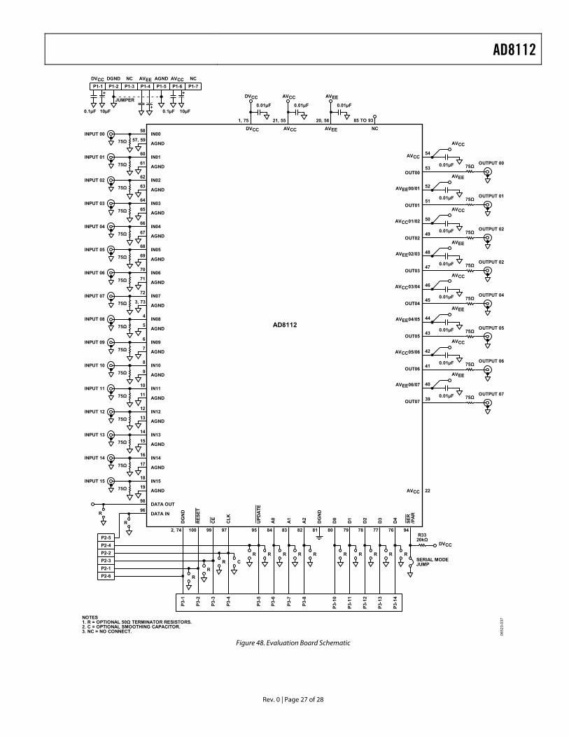
0652
3-03
7NOTES1. R = OPTIONAL 50Ω TERMINATOR RESISTORS.2. C = OPTIONAL SMOOTHING CAPACITOR.3. NC = NO CONNECT.
AVCC
OUT00
54
53
AVCC
0.01µF OUTPUT 0075Ω
AVEE00/01 52
51
AVEE
0.01µF OUTPUT 0175Ω
50
49
AVCC
0.01µF OUTPUT 0275Ω
48
47
AVEE
0.01µF OUTPUT 0275Ω
46
45
AVCC
0.01µF OUTPUT 0475Ω
44
43
AVEE
0.01µF OUTPUT 0575Ω
42
41
AVCC
0.01µF OUTPUT 0675Ω
40
39
AVEE
AVCC01/02
AVEE02/03
AVCC03/04
AVEE04/05
AVCC05/06
AVEE06/07
0.01µF OUTPUT 07
OUT01
OUT02
OUT03
OUT04
OUT05
OUT06
OUT07
22AVCC
75Ω
21, 55
AVCC0.01µF
20, 56
AVEE0.01µF
NCAVCC AVEEDVCC
1, 75
DVCC0.01µF
0.1µF 10µF 0.1µF 10µF
DVCC DGND NC AVEE AGND AVCC NCP1-1 P1-2 P1-3 P1-4 P1-5 P1-6 P1-7
JUMPER
57, 59
58INPUT 00
75Ω AGND
61
60INPUT 01
75Ω AGND
63
62INPUT 02
75Ω AGND
65
64INPUT 03
75Ω AGND
67
66INPUT 04
75Ω AGND
69
68INPUT 05
75Ω AGND
71
70INPUT 06
75Ω AGND
3, 73
72INPUT 07
75Ω AGND
INPUT 0875Ω AGND
5
4
INPUT 0975Ω AGND
7
6
INPUT 1075Ω AGND
9
8
INPUT 1175Ω AGND
11
10
INPUT 1275Ω AGND
13
12
INPUT 1375Ω AGND
15
14
INPUT 1475Ω AGND
17
16
19
18INPUT 15
IN00
IN01
IN02
IN03
IN04
IN05
IN06
IN07
IN08
IN09
IN10
IN11
IN12
IN13
IN14
IN1575Ω AGND
96
98DATA OUT
R
R
DATA IN
P2-5P2-4P2-2P2-3P2-1P2-6
DVCC
SERIAL MODEJUMP
R3320kΩ
2, 74 100 99 97 95 84 83 82 81 80 79 78 77 9476
RRRRRRRRCR
RR
R R
P3-1
P3-2
P3-3
P3-4
P3-5
P3-6
P3-7
P3-8
P3-1
0
P3-1
1
P3-1
2
P3-1
3
P3-1
4
DG
ND
RES
ET
CE
CLK
UPD
ATE
A0
A1
A2
DG
ND
D0
D1
D2
D3
D4
SER
/PA
R
AD8112
+ +
+
85 TO 93
Figure 48. Evaluation Board Schematic
AD8112
Rev. 0 | Page 28 of 28
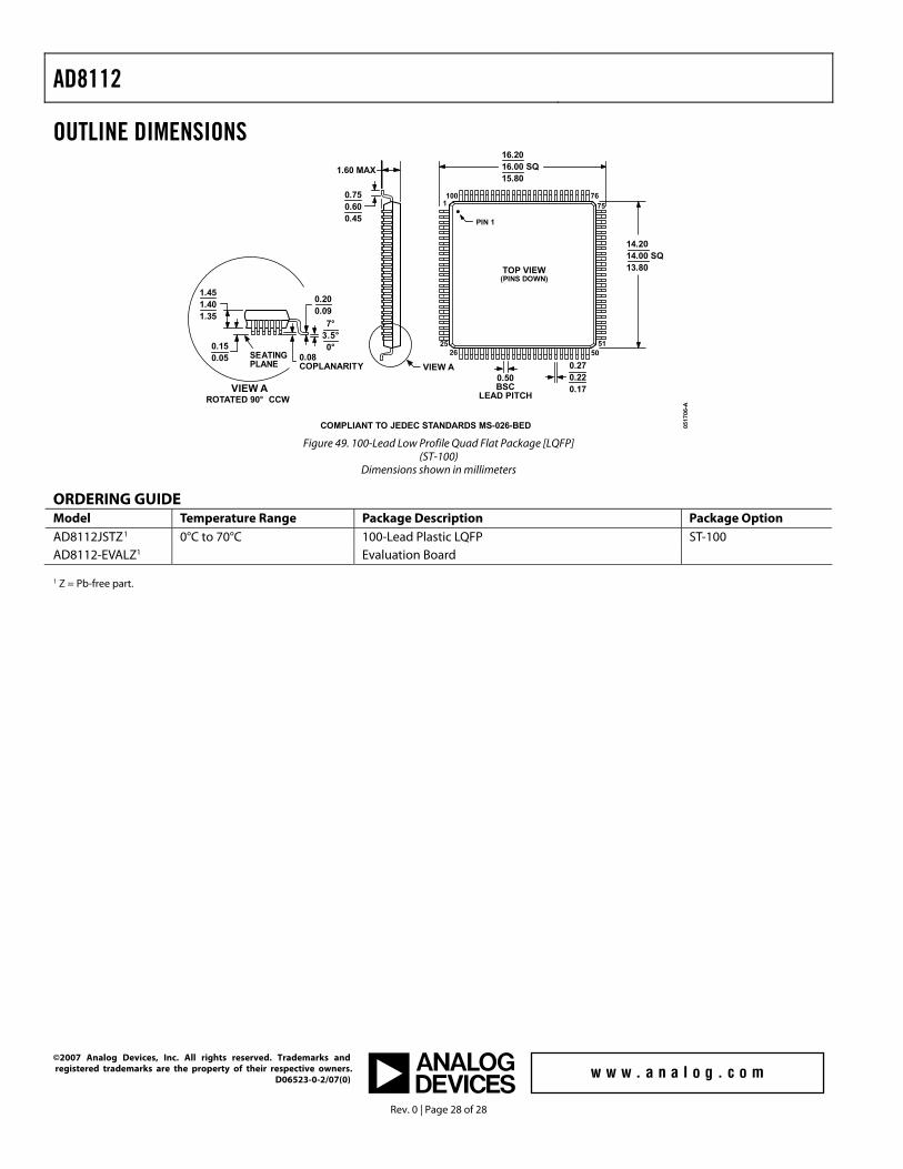
OUTLINE DIMENSIONS
COMPLIANT TO JEDEC STANDARDS MS-026-BED
TOP VIEW(PINS DOWN)
1
2526
5150
7576100
0.50BSC
LEAD PITCH
0.270.220.17
1.60 MAX
0.750.600.45
VIEW A
PIN 1
1.451.401.35
0.150.05
0.200.09
0.08COPLANARITY
VIEW AROTATED 90° CCW
SEATINGPLANE
7°3.5°0°
14.2014.00 SQ13.80
16.2016.00 SQ15.80
0517
06-A
Figure 49. 100-Lead Low Profile Quad Flat Package [LQFP]
(ST-100) Dimensions shown in millimeters
ORDERING GUIDE Model Temperature Range Package Description Package Option AD8112JSTZ1 0°C to 70°C 100-Lead Plastic LQFP ST-100 AD8112-EVALZ1 Evaluation Board 1 Z = Pb-free part.
©2007 Analog Devices, Inc. All rights reserved. Trademarks and registered trademarks are the property of their respective owners. D06523-0-2/07(0)