Embed Size (px)
Citation preview

AD2000 User's Manual
ffi RealTimeDevices, Inc." Accessing the Analog World',"
IISSOO99000011 aanndd AASS99110000 CCeerrttiiffiieedd

A n?nooL .l-Lt -t \t \, \,
User's Manual
ffiREAL TIME DEVICES, INC.
820 North University DrivePost Office Box 906
State College, Pennsylvania 16804Phone: (814') 234-8087FAX: (814) 234-5218

Published byReal Time Devices, Inc.820 N. University Dr.
P.O. Box 906State College, PA 16804
Copyright @ 1990 by Real Time Devices, Inc.All rights reserved
Printed in U.S.A.
Rev.B 9241
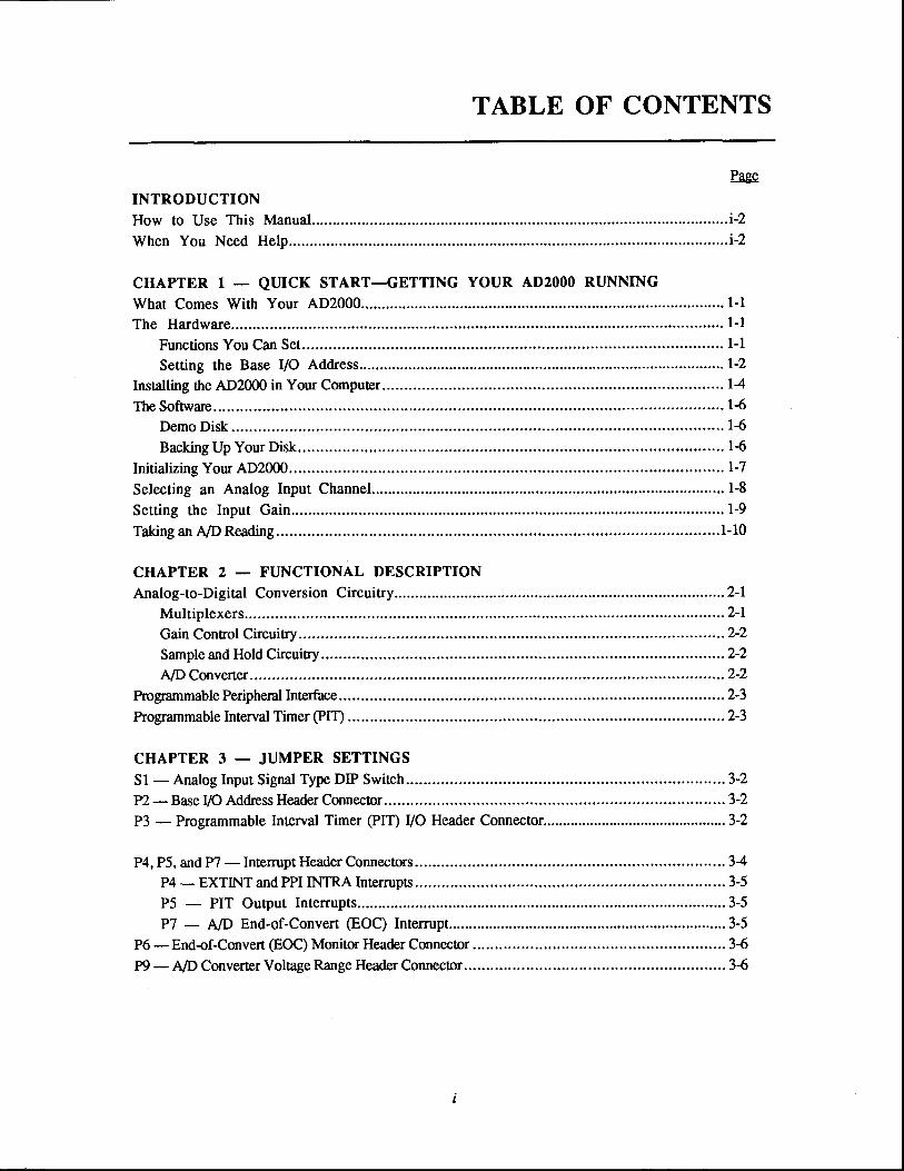
TABLE OF CONTENTS
Page
INTRODUCTIONHow to Use This Manual. . . . . . . . . . . . . . . . . . . . . . . . i -2
When You Need Help. .........i-2
CHAPTER I - QUrCK START-GETTTNG YOUR AD2000 RUNNTNG
What Comes With Your AD2000.. . . . . . . . . . . . . . . . . . . . . . . . . . . . . .1- l
The Hardware.. . . . . . . . . . . . . . . . . . . . . . . .1- l
Funct ions You Can Set. . . . . . . . . . . . . . . . . ' . . . . . l -1
Setting the Base I/O Address .............1-2
Installing ttre AD2000 in Your Computer.... ................... 14
The Software ....... 16
Demo Disk . . . . . . . . . . . . . . . . . . . . .16
Backing Up Your Disk.. . . . . . . . . . . . . . . . . . . . . . . 1{
Initializing Your AD2000 ........l:7
Selecting an Analog Input Channe1................ .............1-8
Sett ing the Input Gain.. . . . . . . . . . . . . . . . . . . . . . . . . .1-9
Taking an A/D Reading...... ....1-10
CHAPTER 2 - FUNCTIONAL DESCRIPTIONAnalog-to-Digital Conversion Circuitry............... ........2-I
Mu l t ip lexers . . . . . . . . . . . . . . . . . . . . . . . . . . . . . . . . . . . . . .2 ' l
Gain Conrol Circui try. . . . . . . . . . . . . . . . . . . . . . . .2-2
Sample and Hold Circuitry..... ..............2-2
AID Converter .................2-2
Programmable Peripheral lnterface...... .........2-3
Programmable Interval Timer (PIT) .............2-3
CHAPTER 3 _ JUMPER SETTINGS
S1 - Analog Input Signal Type DIP Switch.. ................3-2
P2 - Base VO Address Header Connector.... ................... 3-2
P3 * Programmable Interval Timer (PIT) VO Header Connector.... .......................3-2
P4, P5, and P7 - Intemrpt Header Connectors.. .............. 34P4 - EXTINT and PPI INTRA Intemrpts.... ............3-5
P5 - PIT Output Interrupts.... .........3-5
P7 - A/D End-of-Convert (EOC) Interrupt...... .......................3-5
P6 - End-of-Convert (EOC) Monitor Header Connector ..................... 36
P9 - AID Converter Voltage Range Header Connector.... ................... 36

Page
CHAPTER 4 - PROGRAMMING YOUR AD2OOO
Selecting an Analog Input Channe1................ .............4-1
Sett ing the Input Gain.. . . . . . . . . . ' . . . . . . . . . . . . . . .4-1
Taking an A/D Reading...... .....4-1
Programming the Programmable Peripheral Interface................ .......4-1
Programming the Programmable Interval Timer......... ......4'2
Ilardware lntemrpts ............ '....4-3
A/D End-of-Convert (EOC) Signa1......... .................4-3
PPI Intemrps . . . . . . . . . . . . . . . . . .4-3
PIT Intemrps . . . . . . . . . . . . . . . . . .4-3
CHAPTER 5 - CALIBRATION PROCEDURES
RequiredEquipment, . . . . . . . . . . . . . . . . . . . . . . . . . . . . . . . ' . . 5-1
A/D Catibrat ion.. . . . . . . . . . . . . . . ' . . . .5-1
Unipolar Calibration.. .......5-2
Bipolar Calibnation.. .........5-2
Gain Circuiry Calibration .......5-3
APPENDIX A - AD2000 Specifications ...........A-l
APPENDIX B - Connector Pin Assignments.. . . . . . . . . . . . . . . . . . . . .81
APPENDIX C - Component Data Sheets.. . . . . . . . . . . . . . . . . . . . . . . . . . .C-1
APPENDIX D - Configuring the AD2000 for SIGNAL*MATH ..........D-l
APPENDIX E - Configuring the AD2000 for ATLANTIS....... ............E-l
APPENDIX F-Warran ty . . . . . . . . . . . . . . . . .F - l
t l

LTST OF ILLUSTRATIONS
Figurei-11-1L-21-32-l2-23-13-23-3343-5343-73-83-94-r5-1
Page
Typical Laboratory Setup.......... ......i-lAD2000 Board Layout. . . . . . . . . . . . . . . . . . .1-2Base I/O Addres Header Connectff,I2 ................. 14AID Conversion Word Format........ ....................1-10AD2000 Functional Block Diagram ....2-lEOC Timing Diagram. . . . . . . . . . . . . . . . . . .2-zAD2000 Board Layout........ ...........3-lD IP Swi tch 51 . . . . . . . . . . . . . . . . . . . . . . . . . . . . . . .32PIT VO Header Connector I{l ............ 3-3PlTFunctional Block Diagram ..........34IntemrptHeaderConnecorP4 ...........3-5Intemrpt Header Connecor P5 . . .. .. .. . . . 3-5Interrupt Header ConnectorPT ........... 3-6EOC Monior Header Connector P6.............. ........ 36AID ConverterVoltageRangeHeaderConnectorP9 .................. 3-6PPI Mode Definition Format........ .....4-2AD2000 Board Layout. . . . . . . . . . . . . . . . . . .5-1
, l t

i v

LIST OF TABLES
Table
1-1t-25-15-2
Page
AD2000 Board Functions and Settings .................. 1-3
AD2000 VO Map...... .... 1-5
A/D Converter Bit Weights ............... 5-3
A/D Converter Readings for Gain Calibrarion.. ....... 5-3


INTRODUCTION


This manual shows you how to operate and provides technical data for Real Time Devices' AD2000 multifunction dataacquisition board. The AD2000 features 12-bit high-speed multichannel differential or single-ended analog-o-digitalconversion. This versatile interface allows your IBM PCIKT/AT or compatible computer to effectively operate in thereal-time environment of data acquisition and control to sense and generate analog and digital signals. Figure i-l showsa typical laboraory setup using a PC for data collection.
[RSORnT0RT rU0SKSrnrl 0N
llflf,OtltflRt tBM PC orCompEt ib le
Slgnal condl t lon lng D scguis l t lon, dota reduct lon,grdphlcs, onalgsls, conlrol, data storsge
LRBOERTORT RUTOHRTION
sIrTUf nE
Fig. i-1 - Typical Laboratory Setup
The AD2000 features a high-resolution (12-bit) analog-to-digital and converter, digital VO, and timer/counters thatprovide flexibility for many applications. Its six-layer construction, including sep:uate power and ground planes,enhances board performance and low-noise characteristics. It plugs directly into any unused expansion slot (short or full-size) in the computer. All external I/O connections, including PC bus-sourced power, are accessible at the rear panel ofthe computer when the board is installed.
Several of ttre AD2000's functions can be readily adapted for your specific requirements. Through programming and/or jumper or switch settings made on the board, you can:
. Select the base VO address,
. Choose 8 differential or 16 single-ended analog input channels,
. Select the active channel,
. Select the channel gain,
. Select the analog input voltage range and polarity,
. Conrol 16 TTL/CMOS-compatible digital VO lines,
. Control three l6-bit, 8 MHz timer/counter circuits (the programmable interval timer),
. Monitor the A/D conversion using the end-of-convert (EOC) signal,
. Generate intemrpt signals.
Many of these functions are set up at the factory, based on typical data collection requirements and customerspecifications when ordering. Therefore, you can successfully install and run the AD2000 with minimal understandingabout changing and controlling them. On the other hand, you may want to understand everything ahut your boad sothat you can effectively use each feature. With this in mind, this manual provides basic information to get the board upand running, as well as detailed information for a full understanding of each function.
i-1

How to Use This Manual
This manual is designed to help you install and get your AD2000 running quickly, while also including sufficient detailabout each board function. Begin by reading Chapter I in order o use your board as quickly as possible. This chapterand theaccompanyingdemonstration software includedwith yourAD2000packagewillallow you to promptlyuseyourinterface. To fully understand and control the AD2000 functions, read Chapters 2 through 4. Chapter 5 contains boardcalibration procedures.
The chapters and appendixes in this manual are described in denil below.
Chapter 1, "Quick Start--Geuing Your AD2000 Running," provides the instructions necessary toinsall the board and use its basic functions. The information contained in this chapter does not coverhow !o change the board seurp, except for the base ICI address.
Chapter 2, "Functional Description," provides a block diagnm and a functional discussion of theboard.
Chapter 3, 'Tumper Settings," describes each header or jumper circuit on the board and how it iscontrolled.
Chapter 4, "Programming Your AD2000,' describes how the board can be programmed using thedemonstration software.
Chapter 5, "Calibration Procedures," provides instructions for board calibration.
Appendix A, "AD2000 Specifications," contains a complete listing of board specifications.
Appendix B, "Connector Pin Assignments," conlains the pinous of the external VO connecors andthe mating connectors' part numbers.
Appendix C, 'Component Data She€ts," contains manufac[rers' data sheets for major boardcomponents.
Appendix D, "Configuring the AD2000 for SIGNAL*MATH," contains information about seuingboard jumpers and and initializing the board to run the SIGNAL*MATH acquisition and analysisprogram.
Appendix E, "Configuring the AD2000 for ATLANTIS," coniains information about setting boardjumpers to run the ATLANTIS data acquisition and real-time monitoring program.
Appendix F, "Warranty," contains board warranty information.
When You Need Help
When you are working with the AD2000 interface board, this manual and the demo software included in your packagewill provide sufficient information to properly connol all of the board's functions. If, however, after carefully reviewing1fus 66p'ral, you areunable toobtain properresponses from theboard,Real TimeDevices' technical staff isready oassistyou. For assistance, call (814) 234-8087 during regular business hours, eastern standard time or eastern daytght time,or send a FAX requesting assistance to (814) 234-5218. Be sure !o include your company's name, your name, yourtelephone number, and a brief description of the problem.
i-2

CHAPTER 1
QUICK START_GETTING YOUR AD2OOO RUNNING


To get started using your AD2000 interface board, you must:- Select by jumper a base I/O address which does not contend with any ottrer peripheral device.- Install the board ino your PC.- Connect a signal to one ofthe analog input channels.- Run the AD2000 software.
Unless you have other requirements, these steps are all that are necessary to use your AD2000 board.
This chapter explains how to insrall yoru AD2000 and use its basic functions. You will learn how to:. Change the base VO address setring,. Install the board in your PC,. Initialize the board,. Select the analog input channel and gain,. Take an A/D reading.
This chapter allows you to immediately start using the basic functions of your AD2000 board for daa collectionapplications. This chapter does not explain how !o control the more intricate board functions such as the programmableinterval timer, thevariousdigital VO configurations,orintemrpts, nordoes itexplain how to change hardware-controlledseuings except for the base I/O address. The functions not covered here are described in Chapters 2 through 4.
What Comes With Your AD2000
The standard AD2000 board package includes:
1 AD2000 5.5-inch (1a0mm) interface board (fits short slot)I AD200OdemodiskI user's manual
Additional items, such as the AD2000 2-cable set (order number XK40-l), extender boards or SIGNAL*MATH orATLANTIS application software, are available for this board and are included on an as-ordered basis.
All signals on your board are made easily accessible with Real Time Devices' XB40 VO extender board and XC40expansion cable. The extender board has two 20-pin terminal strips and a prototype area to support any special circuitryyou may require to condition the signals. For example, if you are prototyping solid-state relays or optoisolalors, this caneasily be done with an XM0. The expansion cable terminates in a 40-pin wire-wrap header connector suitable forinstallation in standard 0.1 inch spacing perf-board material available from most electronic disributors.
The Hardware
The AD2000 interface board is shown in Figure l-1. A complete listing of the board specifications is contained inAppendix A. The AD2000 has several features which are user-controlled through hardware or software. Most of thehardware-controllable features are jumper-contnolled; the remaining are switch+onnolled.
Allofttreboardcomponentsaremountedona5.5-inchprintedcircuitboardwhichfitsinany unusedexpansion slot(shortor full-size) in an IBM PC/XT/AT or compatible computer. Two 4Gpin connectors on the board, P8 and Pl5,accommodate all of the board's extemal I/O. In operation, these connectors are cabled so that all S0lines are accessibleat the rear panel of ttre computer (see the board installation instructions later in this chapter).
Functions You Can Set
To allow the AD2000 interface board to be adapted to your needs, several functions can be set up to perform specifictasks by changing the hardware configuration or through software. Table l-1 lists each function you can control, thefacory (or default) setting if applicable, and where in this manual you can find information about its settings.
l - l

*-Sy-1lU;tH.t5= U LlH l-.2-r ;--7=,. l+ I* * - l
- -ru tui=sr A -F-"-r E? EIJ=Ff,--d
12-Bit A/D Board
t P 2
:nlilc -
Fig. 1-1 - AD2000 Board Layout
The functions which you can control through hardware are:- Base I/O address,- Analog input channel type,- Analog input channel voltage range and polarity,- End-of-convert. monitor,- PIT timerrcounters (hardware and software),- Intemrpts.
The functions which you can control through software are:- Analog input channel selection,- Analog input gain selection,- Digital VO,- PIT timer/counters (software and hardware),- Board initialization.
Setting the Base VO Address
Starting with thebasel/O address (BA), the AD2000boarduses 12 address locations in yourcomputer's I/O space. Table1-2 lists the VO map for the AD2000. It is important to recognize that some of your computer's VO address locationswill already be occupied by internal I/O and other peripherals. If your AD2000 board tries to use I/O address locationsalready in use by another device in your syst€m, address contention will result. Hence, the board will not operate, or atbest will operate erratically.
VO address contention is one of the most common problems encountered when adding an interface device to yourcomputersystem.Toavoidthisproblem,abaseVOaddrcssjumpercircuitisprovidedontheAD2000board. By changingthe position of the jumper on the header connector labeled P2 Qocated just to the left of center, near the botom of theboard), the base I/O address setting can be changed to any one ofeight locations.
L-2

Table 1-1-AD2000 Board Functions and Sett lngs
FUNCTION FACTORY SETTING USER INFORMATION
Base l/O Address
Analog Input Channel Type
Analog lnput ChannelSelection
Analog lnput Gain Selection
Analog lnput Voltage Rangeand Polarity
End-of -Convert ( EOC) Monitor
Digitall/O
16 l/O Lines from PPI
Programmable Inverval Timer(PlT)Circuitry
Modes
l/O Conliguration
Interrupts
8 differential channels
300 hex (768 decimal)
Software-control lable
Software-control lable
User-specified when ordering
Connected to PA7
Software-control lable
Soflware-control lable
Clock lnput:5 MHzGate Input: +5 VClock Output: To PB
Disabled
To change this setting, see"Setting the Base l/OAddress," Chapter 1
To select 16 single-endedchannels, see S1 discussion,Chapter 3
See "Selecting an AnalogInput Channel," Chapter 1,and demo disk
See "Setting the Input Gain,"Chapter 1, and demo disk
To change these settings, see51 and P9 discussions,Chapter 3.
See P6 discussion, Chapter 3.
See "Programming the PPl,Chapter 4 and demo disk
See "Programming the PlT,"Chapter 4 and demo disk
See P3 discussion, Chapter 3
See P4, P5, and P7discussions, Chapter 3, and"l nterrupt Considerations,"Chapter 4
l-3

Figure I -2 shows the base I/O address header connector, P2, with the jumper installed at the factory-set location of 300hex. Thejumper mustbeinstalledvertically acrossone of theeightpairsof pinsonP2. The hexadecimalbaseVOaddresssetting conesponding to each pair of pins, from left to right, is as follows:
For example, if the base I/O address is changed to 280 hex, then for the 12 operations listed in Table 1-2, BA equals 280.Thus, to send the channel selection and gain data to port B of the PPI, its address of BA + 1 becomes 281 hex.
If thefactory setting of 300 hex will cause contention in yoursystem, position the jumperto the desired base VO addresssetting. Once you have set the base I/O address, make a note of its value on the table inside the back cover of this manual.You will need to know this setting for use in your programs.
Fig. 1-2 - Base l/O Address Connector, P2
Installing the AD2000 in Your Computer
Before installing the AD2000 in your computer, make sure that the base I/O address has been properly selected and allthe hardware settings have been configured o support yourrequirements. This chapterexplains how to control thebaseVO address. Other hardware settings are set at the factory, as listed in Table 1- 1 , and remain at their factory settings unlessyou change them. The intemrpts generated by your AD2000 are disabled (not connected) when you receive your board.If you intend to use the intemrpts, they mustbe configured appropriately before installing the board.Information aboutthese and other functions not covered in this chapter is provided in Chapters 2 through 4. Use these chapters as necessaryto configure your board before installation.
To install your AD2000, follow these step-by-step procedures:
1. TURN OFFTIIE POWER TO YOUR COMPUTER FIRST. Refer to the owner's manual for yourcomputer, and remove the top cover.
2. Select an unused expansion slot (short or full-size) in which to install your board and remove itscorresponding blank bracket from the rear panel of the computer by removing tte screw at thetop of the bracket.
3. Before placing the board into the computer, two ribbon cable assemblies must be inslalled onboardconnectorsPS andPl5.Ifyouhavepurchased the AD2000 cableset, firstinstall thetwistedpair cable on analog VO connector P8. Then install the standard cable on Pl5. Each cable is a4Oline external VO cable which extends through the connector slot in the rear panel of thecomputer. Both cables run through a single slot where they provide 80lines of external I/O totheboard. Thisconfiguration allows substantialboard I/O throughasingleexpansionportin yourcomputer. Appendix B lists the signal carried on each pin of these conneclors. To install thecables:
a. Remove the strain relief clamp attached to the AD2000 bracket located on the right side ofthe board.
b. Connect the socket connector to board connector for each cable. When installing, observethe connector keying and press firmly to make sure that the socket connector is fully seatedon the board. Each cable provided is labeled with the connector's P number for easyidentification. The cables have strain reliefs on one connector and not on the other. Theconnector without the sFain relief is to be installed on the board. After both cables areinstalled on the board, position them so that they pass over the flange in the board's bracket.
3C03803403002C0280240200
g)oo
Noo
t-4
P2
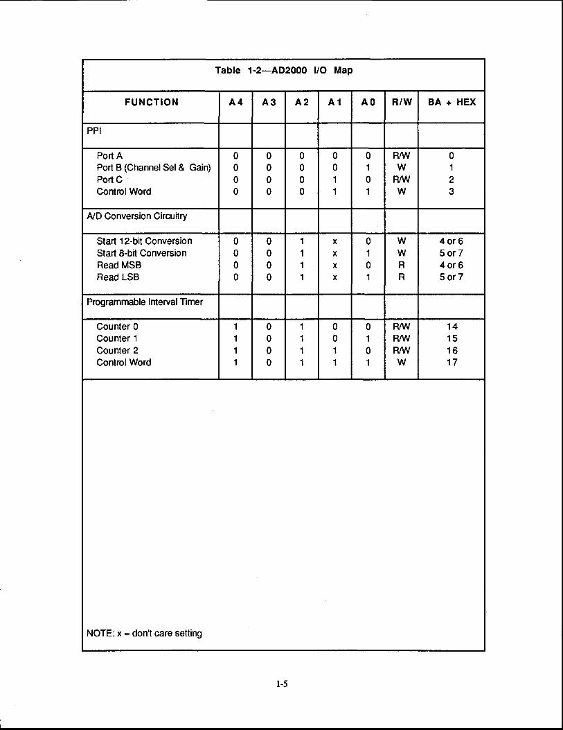
Table 1-2-AD2000 l/O Map
FUNCTION A4 A3 A2 A1 AO R/W BA + HEX
PPI
Port APort B (ChannelSel& Gain)Port CControlWord
0000
0000
0000
0011
0101
R/WW
R/Ww
0123
l/D Conversion Circuitry
Start 1 2-bit ConversionStart 8-bit ConversionRead MSBRead LSB
0000
0000
1111
xxxx
0101
wwRR
4or65 o r74o r65o r7
Programmable lnterval Timer
Counter 0Counter 1Counter 2ControlWord
1111
0000
1111
0011
0101
R/WR/WR/WW
14151617
NOTE: x = don't care setting
l-5

c. Re-at6ch the clamp to the bracket using the hardware supplied with your AD2000, securingthe ribbon cables in place.
4. l.J:ter checking that the cables are correctly installed on the board, orient the board inside thecomputer so that the cables extend through the rear panel opening and the card edge connectorlines up with the expansion slot connector. Then, press down on the metal bracket tab and thetop of the board until the board is firmly seated in the expansion slot connector.
5. Secure the bracket back in place with the screw and put the cover back on your computer.
Now your board is ready to be connected via the external connectors at the rear of the computer. After these connectionshave been made, the board is ready for operation.
The Software
The AD2000 operates under software control. Programming includes the analog input channel selection and gain,control of the the A/D conversion, the programmable peripheral interface, and the programmable interval timer. Theanalog input channel and gain selections and taking an A7D reading are covered in this chapter. Digital I/O control andcontrol of the programmable interval timer are more complex, and are de.scribed in Chapter 4, "Programming YourAD2000."
Regardless of what programming lang"age you use, you can write programs tlat conEol the AD2000 board. Thedemonstration disk which accompanies your AD2000 contains examples in Turbo C, Turbo Pascal, and BASIC.
Nearly all modern MS-DOS-based PC languages have I/O reference instructions. These are the insructions to controlthe data ransfers to and from the I/O ports. Consult your programming language reference to find these instnrctions foryour favorite language. Listed below are the VO reference instructions used by some common languages.
input:
output:
BASIC
INP
OUT
TURBO PASCAL
Port
Port
TURBO CinportbouQortb
Demo Disk
Included with your AD2000 is a demo disk which provides programming instructions and example programs forcontrolling the functions of your interface board. This demo disk is divided ino directories, each of which is namedaccording to the language used to write 0re programs it contains. The files within each directory coniain exampleprograms and a documentation file witi general information. In addition, your demo disk contains a README.DOCfile which provides programming information for your board.
Each example progxam shows you how to control a particular board function, such as selecting an input channel or inputgain, controlling the A/D converter, controlling digital data Eansfers, and seuing the timer/counter circuitry. Theseprograms should be used to become familiar with these functions.
Backing Up Your Disk
The demo disk provided with the AD2000 is a double-sided format which can be read by all DOS versions 1.1 and above.Before using the software included with your board, make a backup copy of the disk. You may make as many backupsas you need. To copy the original to any other DOS-formatted disk, insert the disk o be copied into drive A of yourcomputer, and from DOS enter:
COPY A:*.* B: (or other destination drive specifier)
l -6

Initializing Your AD2000
Before you can operate the AD2000, it must be initialized. This step must be executed every time you start up, reset, orreboot the comput€r. This sets up the PPI to properly communicate with the A,/D converter circuitry. If the board is notinitialized, it will not respond to the software commands and will probably lock up, requiring you to reboot your system.
As described earlier, the AD2000 uses 12 address locations in the computer's I/O space, These address locations startwith tle base I/O address (BA) and go through BA + 17 (hex). BA + 8 through BA + 13 are not used. Table l-2 providesthe AD2000I/O map, defining what function each of the 12 addresses controls. Recall that the base I/O address is factory-set at 300 hex. On the demo disk, the base I/O address is usually stored in the variable "board." Remember to use tlrecorrect base VO address in tle demo disk programs or your own programs. The demo disk explains how to change thebase I/O address in the programs.
The AD2000 is inirialized by simply writing a control byte lo the PPI control register mapped at the VO location baseaddress + 3 (hex). The conrol byte must conform to this general form:
lxxx x00x where x =don'tcare
This ensures that the eight I/O lines making up port B of the PPI, which are used to control the multiplexer and gaincircuitry, are configured as outputs. The don'tcare (x) positions control the direction of the remaining 16 digital I/O linesavailable on the PPI. These lines can be confrgured as inputs, outputs, or in other more complex configurations.
For example, when the control byte bit pattern is:
100000000 (decimal 128)
the AD2000 is initialized as follows:
out base_address+3, I 28
When this value is used to initialize the AD2000, the eight port C lines of the PPI will all be configured as outputs. Youcan transfer data to these lines with the command:
out base_ad&ess+2,data
If instead, the decimal value 137 (1000 1001) is used to initialize the AD2000, the port C lines will be set up as inputs.You can input data from port C with the command:
data = inp(base_address+2)
Note that port A, bit 7 (PA7) of the PPI is factory-set to monitor the end-of-convert (EOC) signal. The PPI must beprogrammed so that port A is an input if you are going to monitor the EOC signal through PA7. The connol byte mustthen conform to the general form of lxx! x00x, where the underlined I is the data bit which sets up port A as an input.
A functional description of the PPI is contained in Chapter2,'Functional Description," andhardwareconfigurations aredescribed in Chapter 3, "Jumper Settings." Information about how you can control the diginl I/O lines is contained inChapter 4, "Programming Your AD2000," and is not covered here because of its complexity.
As mentioned earlier, the eight lines of port B are used to select the analog input channel and gain. The four LSBs, PB(forPortB) 0 throughPB3, control thechannel selection,andthe fourMSBs,PB4 throughPBT,control thegain selection.The bit assignment of this port is:
t-'7

MSBs LSBs7654 3210 PP I Po r tB (BaseAdd ress+1 )\-rJ +.-'
gain select channelselect
0000 = 1x 0000 = channel 10001 = 2x 0001 = channel 20010 = 4x 00100100 = 8x 001 11000 = 16x 0100
01 0101 10011110001 0011010101 11 1001 1011110 = channe l 151111 = channe l 16
After the AD2000 is initialized, the port B register is loaded with the default setting of 0000 0000. This selects channelI as the input channel with a gain of 1. To change this value, for example, lo a gain of2x on channel 16, enter thesecommands:
BA + I (hex) selects port B
0001 1111 sesgainto2xandchannelo 16
Recall that the board's default channel setting is eight differential channels. Therefore, only the channel select binaryvalues forchannels I through 8 apply. Channels 9 through 16 are used in the single-ended channel mode only.Now yourboardis initializedandready ooperate. The following sectionsdescribehow toselecttheanaloginputchannel,set the input gain, and take an A/D reading. Mastering these operations will allow you to effectively use your board fordata acquisition applications.
Selecting an Analog Input Channel
After the AD2000 has been initialized you can select the analog input channel. The analog input channel is selected bywriting !o port B of the PPI, mapped at I/O location base address (BA) + 1.The input channel and the input gain can be set individually by setting only the four LSBs (channel select) or only thefour MSBs Gain) of tie eight-bit control word sent to port B. Before you change either the input channel or the gain,you MUST preserve tle current state of port B. Failure tro do so will result in changing both the channel select and thegain when you intended o change only one of these two settings.
The general algorithm for setting tlechannel (changing just the four LSBs of the control word whilepreserving the fourMSBs) is:
l -8

1. Read the current state of port B:
curent_state = inpoase_address+1)
2. Preserve the upper four bits since they contain gain data:
current_s[ate = current-slate AND $F0
3. Logically OR the current_state with the desired channel number minus 1:
curenr-state = curent_state OR (channel - l)
4. Write it back out to port B:
out base_address+ l,current_state
A BASIC program to select channel 2 is:
100 BASE-ADDRESSTo = 768
110 CHANNELVo =2
120 STATUSTo = INP(BASE-ADDRESSTo + l)
130 STATUSTo = STATUSTo AND &HFO
140 STATUSTo = STATUSTo OR (CHANNELTo -l)
150 OUT BASE-ADDRESSTo + I,STATUSTo
Setting the Input Gain
Thegain is setby writing totheupperfourbitsofportB atBA + l. Thebitpattern foreach of thefivegain values supportedby the hardware are:
0000 = gain of I
0001 = gain of2
0010 = gain of 4
0100 = gain of 81000 = gain of 16
It is recommended that no other bit patterns be used when setting the gain.
The general algorithm for setting the gain is:
1. Read the current state of port B:
current-state = inp(base_address+ 1)
2. heserve the lower four bits since they contain channel information:
current-sCate = CUrrg[t-State AND $0F
3. Ingically OR the curent_state with a bit pattem that activates the desired gain:
current_state = currgnt_State oR gain bit pattern:
lx bit pattern = 0
2x bitpattern = 16
4x bit pauern = 32
8x bit Pattern = 64
l6xbitpattern = 128
4. Write the current_state back to port B:
out base_addrcss+ l,current-state
r-9

A BASIC program to set a gain of 2 is:
100 BASE-ADDRESSTo = 768
110 GAINTo = 2
120 STATUSTo = INP(BASE-ADDRESSTo + l)
130 STATUSTo = STATUSTo AND &H0F
140IF GAINTo = I GOTO 160
150 STATUSTo = STATUSTo OR (GAINTo * 8)
160 OUT BASE-ADDRESSTo +I,STATUS 7o
Taking an A/D Reading
After you have selected an analog input channel and set the gain, you can take an A/D reading. It is important to notethat once the gain and channel are set, they stay at those settings until you change them; that is, they are latched. Youdo not have to set the gain or channel every time you take a reading.
Each time an A/D conversion is completed, an end-of-convert (EOC) signal is generated to signify the end of theconversion. This signalcanbe usedinanumberof ways. Oneway is to use this lineto monitortheAlDconversion status.SeninguptheEOC signal obe monitoredinvolvesconfiguringbitT ofPPlportAorportC as an inputlineand connectingthe E@ signal to it. This procedure is detailed in Chapter 3,'Tumper Settings." The EOC signal is factory-set to bemonitored through PA7 on header connector P6.
The general algorithm for taking an A/D reading is:
1. Start a l2-bitconversion by writing o base-address + 4 (or 6):
out base-address+4,0(Note that the value you send is not important. The act of writing to this I/O location is the key
to starting a conversion.)
2.Delay at least 20 microseconds or monitor PPI port A or C, bit 7 for a transition. Pollingpermits the fastest data acquisition.
3. Read the least significant bit from base-address + 5 (or 7):
lsb%o -- inp(base-address%o +5)
4. Read the most significant bit from base_address + 4 (or 6):
msbTo = inp(base-address7o +4)
5. Combine them into ttre 12-bit result by shifting the LSB four bits o the right. The MSB mustalso be weighted conectly:
resultVo - (msb7o * 16) + (lsb7ol 16)
For a l2-bit conversion, the A/D data read is left justified in a l6-bit word, with the least significant four bis equal tozero, as shown in Figure l-3. Because of ttris, the two bytes of A7D data read mustbe scaled to obtain a valid A/D reading.Once it is calculated, the reading canbe correlated lo a voltage value by scaling it, in the case of bipolarinputranges (t5or +10 volts), and then multiplying by the appropriate bit weight, as shown in the table at the top of the following page:
MSBD15 014 D13 D12 D11 D10 D9 D8 D7 D6 D2D3D4D5
LSBD1 DO
l -10
DB12DB1 1 DBlO D89 D88 D87 D86 D85 D84 D83 D82 DB1 0 0 0 0
Fig. 1-3 - A/D Conversion Word Format

Input Range Scale Factor Bit Weight+5 volts Subtract 2M8 2.4414 mY+10 volts Subnact 2048 4.8828 mV
0 to +10 volts None 2.4414mY
For example, if the A/D reading is 1024 and the input range used is *5 volts, the analog input voltage is calculated asfollows:
00z. - 2&18) bits * 2.4414 mv/bit = -2.49999 volif,.
For a tlO volt input range, the voltage is calculated as follows:(l0U - 2048) bits * 4.8828 mv/bit = -4.99999 volts.
For a 0 to +10 volt input range, no scaling is required and the voltage is calculated as follows:
1024 birs * 2.4414 mV/bit = 2.49999 volrs.
The input voltage range and polarity are factory-set according to customer specifications when ordering the board. Ilafterreceivingyourboard, you wish tochange the inputvoltage, seeChapter3,'TumperSettings."Wheneverthevoltagepolarity is changed (unipolar to bipolar or vice versa), the A/D converter should be recalibrated as described in Chapter5, "Calibration hocedures."
Note that eight-bit A/t) conversions can also be performed. This is accomplished by writing to I/O location BA + 5 (or7). While an eight-bit conversion has a lower resolution than the 12-bit conversion, it is performed much more rapidly,in about 13 microseconds. A 12-bitconversion takesabout20 microseconds. Therefore, when speed is essential, you canuse the eight-bit conversion capability.
t - 1 1


CHAPTER 2
FUNCTIONAL DESCRIPTION


This chapterdescribes the majorfunctions of theAD2000interfaceboard. Figure2-1 shows ablock diagnm of ttteboard.The functions discussed in the following sections are:
. Analog-to-digital conversion circuiry
. Programmable peripheral interface (PPI) circuiry
. Programmable interval timer (PIT) circuitry
Analog-to-Digital Conversion Circuitry
The main function of the AD2000 interface board is to provide high-speed analog+odigital conversion capability fordata acquisition. The analog-to-digital (AlD) conversion circuitry receives inpus from eight differential or 16 single-endedanalogchannels, selects oneactivechannel, andperforms an analog-to-digital conversion of thevoltage valuereadat that channel. The conversion throughput rate is typically 38 kIIz.
Multiplexers
Two eight-bit analog multiplexers are used to connect either one of 16 single-ended or one of eight differential analogchannels o the gain circuiry. The leftmost three switches on DIP swirch S 1 set up the multiplexer at IC location U9 !oreceive either single-ended or differential inputs. When these three switches are up, the multiplexer is configured forsingle-ended inputs, and when they are down, the multiplexer is configured for differential inputs. Note that these threeswirches are always set as a gloup to the same position (see "Sl Switch Settings," Chapter 3). A channel is selectedthrough software control, by writing to port B of the PPI, as described in Chapter l.
16 AilAlG NruTS€V TO +$r0 TO +10\,
-'l0V TO +t0VtlFF. / t5 s.t
Fig.2-1- AD2000 Functional Block Diagram
2-l

Gain Control Circuitry
The programmable gain control circuiry can provide a gain factor of 1 ,2,4,8,or 16. The gain selection is made by writingto port B of the PPI, as described in Chapter 1. The gain facor is conrolled by the setting of four analog switches. Foragainof 2,4,8, or 16, this writeoperation will closeone of thefourswitches; foragain factorof 1, all switches are open.Note that programming gain facors other tlnn the five listed here is not recommended.
Sample and Hold Circuitry
A sample and hold (SAD amplifier is used benveen the gain control circuiry output and tlte A/D input to ensure thatdynamic analog signals are accurately digitized by the A/D converter. The .001 pF hold capacitor used in this circuit isa polystyrene type selected for is low dielecnic absorption. Its low value minimizes the acquisition time (6 microseconds,typical),andminimizeshold step voltageanddroop.Thesampleandholdtimeandratearedeterminedby theEOC signalgenerated by the A/D converter and fed back into the SAI circuir When the EOC signal is high (logic 1), the amplifiersamples the analog inpuq when the EOC signal is low (logic 0), the amplifier holds the inpur
A"/D Converter
The A/D converter is a high-speed l2-bit conversion IC which performs conversions in approximately 20 microseconds.Eight-bit conversions can also be performed when speed is more critical than resolution. An eight-bit conversion takesabout 13 microseconds, allowing rapid conversions of dynamic analog inputs. The converter supports 10- or 20-voltanalog input signals; however, it cannot support a 20-volt unipolar input range because its supply voltage in the AD2000application is only +12 volts. The analog input voltage nmges supported by the AD2000 are listed in the specificationsin Appendix A. Calibration circuiry is included for unipolar and bipolar calibration of the A/D converter. Calibrationprocedures are described in Chapter 5.
An 8- or 12-bit conversion is initiated by a write operation to the appropfutelO address. Once a conversion is begun,the conversion status can be monitored by reading the AID converter status (STS) signal which is ouput from the A/Dconverter IC and inverted before being made available to other circuitry on the board as ttte end-of-convert @OC) signal.The EOC signal can be monitored by one of nro digital input lines on the PPI, PA7 or PC7. Note that if either line isselected as the EOC monitor, a jumper must be installed for the selected line on P6 and that line must be configured asan input. The EOC signal is factory-set to be monitored through PA7 on P6. The EOC signal is low (logic 0) during aconversion. Figure 2-2 shows the EOC timing diagram. Also, the three-state A/D output buffers remain in a high-impedance state, and, therefore, datacannotberead. Whileaconversion is inprogress, any transitions of the digital inpuswhich control the conversion will be ignored, so that the conversion cannotbe prematurely terminated or restarted. Oncethe conversion is complete @OC is now high, or logic 1), the A/D data can be read in two bytes, the MSB and the LSB,in any order. Fora l2-bitconvenion, tie datais left-justified in a l6-bit word. In the case of an eight-bitconversion, thedata is completely contained in the eight-bit MSB.
Refer to Chapter l, "Taking an A/D Reading," and the demo disk for more information about using the AID converter.
A/Dcs v
t lEoc- f i-r---,
Data 14
Fig.2-2 -EOC Timing Diagram
a a

Programmable Peripheral fnterface
The hogrammable Peripheral Interface @PI) provides 16 TTL/CMOS digital VO lines which can be configured in anumber of ways to support user requirements. The lines available for digital I/O are port A and port C. The 8255 PPI hasantalof 24 digital I/O lines, eight of which are used to connol the A/D channel selection and gain circuiry, and thereforeare not available to the user. Theremaining 16lines are available atextemal VO connecor Pl5. The 24lines are groupedinto three eight-bit ports, port A, port B, and port C. Port C is further suMivided into two four-bit ports, port C lower(PC0-PC3) and port C upper (PC4-PC7) in certain modes of operation. The PPI data sheet is included in Appendix C.
The eight bits ofport B are reserved for A/D channel selection and gain control, and cannot be configured for I/O use.Ports A and C can be configured in any of the three operating modes described below:
Mode 0 - Basic input/outpur Provides simple input and output operat"ions for each port. Data iswritten to or read from a specified port.
Mode I - Srobed inpuUoutput. Provides a means for transferringlO datz to or from port A or portB in conjunction with strobes or handshaking signals.
Mode2 -Suobedbidirectional input/output. Provides abidirectional means of communicating withanother device on a single eight-bit bus. Handshaking signals are similar to mode 1. This mode appliesto port A only.
In mode 0, all four ports (A, B, C lower, and C upper) are available as VO lines. Sixteen configurations are possible intlfs mode, andany portcan be configuredas an inputoran output. The ouputs are larched,butthe inpusarenotlarched.
In mode I , the four ports are gfouped into two groups. Each grcup contains one eight-bit data port (port A or port B) andone four-bit control/data port (port C lower or port C upper) which is used for control and status of the eight-bit port. Theeight-bit data port in each group can be configured as an input or an outpul Both inputs and outputs are latched.
In mode 2, port A is an eight-bit bidirectional bus and port C is a five-bit control port Port B cannot be used in this mode,but is available for use in mode 0 or mode I while port A is in mode 2. Both inputs and outputs are larched.
The PPI is configured by writing a control word to the appropriate VO address location, as described in Chapter 4,"Programming Your AD2000."
The control word can also be used to individually set or reset the port C bis. This feature allows any bit of port C to beset or reset without affecting the other port C bits. The data sheet included in Appendix C explains this feature.
ThePPIcan alsobe used o generateinterupts in mode I or mode2 operation.In these modes, theintemrptenable (INTE)mask is used to enable the INTRA and INTRB interrupt signals. Note ttrat the INTRB signal for PPI cannot be used sinceport B of this PPI is always configured as mode 0 output and is reserved for channel selection and gain control. Intemrptfunctions are further explained in the data sheet in Appendix C.The AD2000 board provides a header connector which can jumper the A/D converter end-of-convert (EOC) signal !oa PPI bit where it can be monitored to provide A/D conversion status. The EOC signal can be jumpered to either PA7(port A, bit 7) or PC7 (port C, bit 7). The default setting of the jumper is PA7. The port used to moni[or ttre EOC signalmust be configured as a mode 0 input port.
Programmable Interval Timer (PIT)
The programmable interval timer @IT) can be configured for a variety of timing and counting functions. This versatileIC contains three independently clocked l6-bit timer/counter circuis, TC0, TCl, and TC2, which operate as downcounters. These down counters can resolve time increments down to 125 nanoseconds. This circuit's most commonapplication is to provide accurate time delays under software control. Upon command, the PIT can count out aprogrammeddelay andinterruptthePC when ithas finishedits tasks. All threecounteroutputsarebroughtouttoexternalI/O connector P15.
The three 16-bit timer/counters are each loaded by two one-byte write operations to the appropriate I/O location. firebytes are latched into a l6-bit internal countregister, where they are stored until the count sequence starts. The countdownstafis when the count register contents are transferred (in parallel) to the down counter. The timer/counter circuits canbe programmed for binary or BCD countdowns.
2-3

A 5 MlIz crystal oscillator on the AD2000 can be used to clock any timer/counter circuit Or, the timer/counter can beclockedby asource external to theboard through external VO connectorPl5. Rates of dc to 8 MIIzcan beused aoclockthe timerrcounters.
Each timer/counter can be configured for one of six modes of operation. These modes are:
Mode 0 - Interrupt on end of count. The OUT signal changes from low to high when tlte countdownis completed.
Mode 1 - Re-triggerable one-shot. A low-level pulse riggered by the GT input is output on the OUTpin.
Mode2-Rategenerator.
Mode 3 - Square wave generator.
Mode 4 - Sofnrare-triggered strobe.
Mode 5 - Hardware-triggered strobe (re-triggerable).
The timer/countercountmodes, as well as the counttype (binary or BCD), read/write mode,and counter/timerselectionmode, are all part of the control word which is written o the PIT control register to initialize tle circuir When the PCis powered up, the timer/counter circuits are not defined until the appropriate control words are written to the circuits !oprogram them foroperation.Initializationisrequired only onceafterapower-upresetoccurs. Detailedinformation aboutthe PIT, including the connol word format, is given in the data sheet in Appendix C. Appendix D contains programmingnotes for some PIT applications.The three timerrcounter circuifs are independent. However, they can be cascaded for countdowns which are longer tlnnone 16bit field can supporL For example, TCO'S OUT signal can be connected to TCI's CK signal, and TCl's OUTsignal can be connected to TC2's CK signal. When configured ttris way, the PIT can accommodate extremely longcountdowns. This configuration is described in the application notes in Appendix D.
One of the three timer/counter outputs, TCO OUT, TCI OUT, or TC2 OUT, can also be used as a PC intemrpt. Thesesignals are brought out to board header connector P5 where one (and only one) can be. selected for connertion [o any oneIRQ channel, RQ2 through IRQ7. Chapter 3, "Jumper Settings," and Chapter 4, "Programming Your AD2000,"describe these intemrpts in more detail.
24

CHAPTER 3
JUMPER SETTINGS


This chapter describes the AD2000 board settings you can control on DIP switch S I and various header connectors. Youcan use this chapter to tailor your board's functions to your specific application before installing it in your computer, orto change the board's configuration as you learn more about. its operation and special features. In this chapter, you willleam about each setting and how to set switches or install jumpers to achieve the desired operation of your board. Beforechanging any settings, you should have a functional knowledge of the circuit you are setting up (see Chapter 2).Remember that all of the settings described in this chapter have been faclory-set, or, as in the case of the intemrpt signals,are disabled. Therefore, you do not have to do any further set-up of ttre board in order for it to operate in your systemas described in Chapter 1. The descriptions in this chapter allow you to change factory settings, or to tailor your boardto take full advantage of its built-in versatility.
There are one DIP switch and several header connectors which allow you to control various board functions. These areshown in the board layout of Figure 3-l and are presented as follows:
Sl * Analog Input Signal Type DIP Switch
P2 - Base I/O Address Header Connector
P3 - Programmable Interval Timer (PIT) I/O Header Connector
P4, P5, and P7 - Intemrpt Header Connectors
P6 - Endof-Convert (EOC) Monitor Header Connector
W - A/D Converter Voltage Range Header Connector
Fig. 3-1 - 4D2000 Board Layoul
H,H'Flffiffif\ I WPE POL CA
G
Y r 6 . \ t
l "ll-lilll l:;rTld=J ll |;r-"nf tllUilc -
Yl,*jB?."?. pqr (-)c,.
3-1
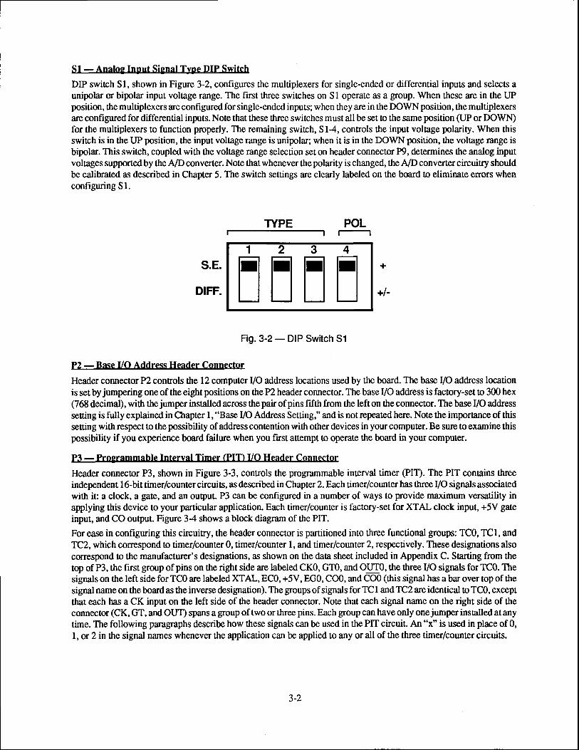
51 - Analog Input Signal Type DIP Switch
DIP switch Sl, shown in Figure 3-2, configures the multiplexers for single-ended or differential inputs and selects aunipolar or bipolar input volage range. The fint three switches on Sl operate as a group. When these are in the UPposition, the multiplexers are configured for single-ended inpus; when they are in the DOWN position, the multiplexersare configured for differential inputs. Note that these three switches must all be set to the same position (UP or DOWN)for the multiplexers to function properly. The remaining switch, S l-4, controls the input voltage polarity. When thisswitch is in the UP position, the input voltage range is unipolar; when it is in the DOWN position, the voltage range isbipolar. This switch, coupled with the voltage range selection set on header connector P9, determines the analog inputvoltages supported by the AID converter. Note that whenever the polarily is changed, the AID converter circuitry shouldbe calibrated as described in Chapter 5. The switch settings are clearly labeled on the board to eliminate errors whenconfiguring S1.
TYPE POL
S.E.
DIFF.
1
NNEE+l-
Fig. 3-2 - DIP Switch Sl
P2 - Base VO Address Header Connector
Header connector P2 controls ttre 12 computer I/O address locations used by the board. The base VO address locationis set by jumpering one of the eight positions on the P2 header connector. The base I/O address is factory-set to 300 hex(768 decimal), wittr the jumper installed across the pair of pins fifth from the left on the connector. The base I/O addressseuing is fully explained in Chapter 1, "Base I/O Address Setting," and is not repeated here. Note the importance of thissening with respect to the possibility of address contention with other devices in your computer. Be sure to examine thispossibility if you experience board failure when you first auempt !o operate the board in your computer.
P3 - Programmable Interval Timer (PIT) VO Header Connector
Header connector P3, shown in Figure 3-3, controls the programmable interval timer @IT). The PIT contains threeindependent l6-bit timer/counter circuits, as described in Chapter 2. Each timer/counter has three VO signals associatedwitlr iu a clock, a gats, and an output. P3 can be configured in a number of ways to provide maximum versatility inapplying this device to your particular application. Each timerrcounter is factory-set for XTAL clock input, +5V gateinput, and CO output. Figure 3-4 shows a block diagram of the PIT.
For ease in configuring this circuitry, the header connector is partitioned into three functional groups: TCO, TCl, andTC2, which conespond to timer/counter 0, timer/counter 1, and timer/counter 2, respectively. These designations alsocorrespond to the manufacturer's designations, as shown on the data sheet included in Appendix C. Sarting from thetop of P3, the first group of pins on the right side are labeled CK0, GTO, and OUTO, the three I/O signats for TCO. Thesignals on the left side for TCO are labeled XTAL, ECO, +5V, EGO, CO0, and C-O0 (this signal has a bar over top of thesignal name on the board as the inverse desigration). The groups of signals for TC 1 and TC2 are identical to TCO, exceptthat each has a CK input on the left side of the header connector. Note that each signal name on the right side of theconnector (CK, GT, and OUT) spans a group of two or three pins. Each group can have only one jumper installed at anytime. The following paragraphs describe how these signals can be used in the PIT circuit. An "x" is used in place of 0,1, or 2 in the signal names whenever the application can be applied to any or all of the three timer/counter circuits.
3-2

XTALEC0+5VEGOco0cTocK1
XTALEC1+5VEG1colco1cK2
XTALEC2+5VEG2c02c02
lslslslsl3
l:lslsls
Fig.3-3 - PIT l/O Header Connector P3
Counter Inputs:
XTAL - This input to all three timer/counter circuits is from the 5 MlIz crystal oscillator, labeled Yl, located in theupperleftareaof theboard. By connecting XTAL to theCKx input on the rightside of the connectorwith ajumperplacedhorizontally between the pins, the 5 MHz clock is applied to the timer/counter circuit. If required by your application,the XTAL frequency can be changed by installing a different crystal oscillaor at Y I . Note, however, that the maximumfrequency at which the PIT will operate is 8 MHz.ECx-This inputallows an external clock, other than the XTAL signal, to control the timing of thecorresponding timer/counter circuir This pin can be horizonally jumpered to the CKx input on the right side of the connector, in place of theXTAL souce. The ECx signals are brought onto the board through external VO connector Pl5 (see Table B-3 inAppendix B).
Gate Inputs:
+5V - This input, if connected o the GTx input by placing a jumper horizontally between the two pins, places theassociated timer/counter circuit in an enabled state at all times.
EGx -This inputcan be horizontally jumpered to the GTx inputon therightside of the connector !oprovide an extemalgate input instead of the +5 volts input TheEGx signals arebroughtonto theboard through external VO connectorPl5(see Table B-3 in Appendix B).
Counter Outputs:
COx - This output can be horizontally jumpered to the corresponding OUT pin on the right side of the connector sothat the clock output signal can be routed to external I/O connector P15 (see Table B-3 in Appendix B).
CO" - This output can be horizonally jumpered to the corrosponding OUT pin on the right sido of the connector toprovide the inverse of the clock output signal to external I/O connectorPl5 (see Table B-3 in Appendix B).
3-3

CKx - This input connects the output of one timer/counter to the clock input of the next timer&ounter. CKx is providedfor TCl and TC2 only, and is connecM to the output of the previous timer/counter (tCO or TCI) by placing a jumperhorizontally between the pins. These connections are used to cascade the timer/counters for longer time delays than aresupported by a single timer/counter circuit.
P15 8255 PtTU5
EC0
EGO
co0
cK l l I
*ro1- -kl-
*sv---Idt)o
<dc-ool o
XTALI
+sv-aQ
<------rcco1l o
P3
EC1
EG1
co1
EC2
EG2
co2
Fig. 3-4 - PIT Functional Block Diagram
P4. P5. and P? - Interrupt Header Connectors
Header connectors P4, P5, and F7 are used to jumper various signals generated by the AD2000 circuitry !o the PC'sinterrupt channels. The intemrpt channels available on the board are IRQ2 through IRQ7. Note that only one intemrptin the computer system can be connected to an intemrpt channel at any given time.
Before attempting to use intemrpts, you should be familiar with the procedure for initializing the intemrpt vectors andthe PC's interrupt controller, and setting up the intemrpt handling routines. These procedures are beyond the scope ofthis manual, but must be understood o effectively use intemrpts in you computer sysiem.Be careful to avoid contention when selecting the intemrpt channels used, both with the signals on the AD2000 as wellas with other devices within your computer. To avoid contention, use the table inside the back cover of this manual torecord ttre intemrpt channels you use with the AD2000 board.
It is also very important to note that the AD2000 intemrpt sources are TTL totem-pole (push/pull) type outputs; they arenot open-collector. Therefore, do not att€mpt to connect one of these intemrpb to any other intemrpt output.
The following paragraphs describe the interrupts available on your AD2000 board.
XTALI Ot>o
..5y-€
{-O.4,to'r-u
34

P4 - EXTINT and PPI INTRA Interrupts
Header connectorP4 is used to selectEXTINT orPPI INTRA for connection to one of the computer's intemtpt channelsIRQ2 through IRQ7. EXTINT is provided to accommodate an interrupt signal generated external to the AD2000 androuted onto the board through external I/O connector P 15 (see Table B-3 in Appendix B). PPI INTRA (labeled PC3 onthe board) is generated by the PPI. This intenupt is generated during PPI mode 1 or mode 2 operation only. One of thesetwo signals can be jumpered to one of the available computer intemrptchannels IRQ2 through IRQT by firstplacing ajumper vertically across ttre pins of the signal chosen and then placing a second jumper vertically across the pins of theselected IRQ channel. Figure 3-5 shows header connector P4 with jumpers installed so that PPI INTRA is connected toRQ2.
IRQ( o t ) s t
P4
Fig. 3-5 - Interupt Header Connector P4
P5 - PIT Output Interrupts
Header connector P5, shown in Figure 3-6, is used to jumper one of the three PIT outputs, OUT0, OUTI, or OUT2, toone of the computer's intemrpt channels IRQ2 through IRQ7. As in the case of P4, two jumpers must be installed toconnectaPlT output to an interruptchannel. First, install a jumperhorizontally across thepins of thePlTouput selected.Then installasecondjumperacross thepins of the intemrptchannelselected. Figure3-6showsjumpen installed so thatOUT2 is connected to IRQ3.
765432ol11821-{
Fig. 3-6 - Interrupt Header Connector P5
Yl - ND End-of-Convert (EOC) Interrupt
Header connector P7, shown in Figure 3-7, is used to jumper the A/D converter's end-of-convert (EOC) signal to oneof the computer's intemrpt channels IRQ2 through IRQ7. The EOC signal is connected to an RQ channel by installinga single jumper horizontally across the pins of the IRQ channel selected. Figure 3-7 shows the EOC signal connectedro IRQ4.
FzF G Ixc )ul o. I\
P5
3-5

765 : 0
4o32
Fig. 3-7 - Interrupt Header Connector P7
P6 - End-of-Convert (EOC) Monitor Header Connector
As described above, the A/D converter end-of-convert @OC) signal can be used to generate an intemrpL If this signalisnotusedasan intemrpt, itcanbe usedas astatusmonitorof theA/Dconversionprocess. HeaderconnectorP6providestwolinesthroughwhich tleEOCcanbemonitoredfromthePPI,PATorPCT. Oneof thesenvodigitall/Olinesisselectedfor EOC monitoring by installing a jumper horizontally across the appropriate pair of pins. The digital VO line selected,PA7 or PC7, must be configured as a mode 0 input (see Chapter 4, "Programming Your AD2000"). Figure 3-8 showsP6 with a jumper installed in the factory-set position for EOC monioring through PA7.
Fig. 3-B - EOC Monitor Header Connector P6
P9 - A/D Converter Voltage Range Header Connector
HeaderconnectorP9, shown inFigure 3-9, is usedtoselecttheanalog inputvoltage range of the A7D converter. Ajumperis installed venically across the pins marked lOV to support a l0-volt range (0 to 10 volts or -5 to +5 vols), or acrossthe pins marked 20V to support a 20-volt range (-10 to +10 volts). The setting of ttris jumper, coupled with the settingof DIP switch S 14 which selecs a unipolar or a bipolar range, determines the input voltage range of the AID converter.P9 is configured at the fac[ory according to the customer's specifications for the input voltage range. The valid seuingsof P9 and Sl-4 are summarized in the able below:
!o
!
{
Range
-5 to +5 vols0 to +10 volts
-10 to +10 volts
P9 Setting
lOv Gish|lOV (right)20V (left)
S1-4 Setting
DOWN Oipolar)LJP (unipolar)
DOWN Oipolar)
Fig. 3-9 - A/D Converter Voltage Range Header Connector P9
3-6

CHAPTER 4
PROGRAMMING YOUR AD2OOO


All communication with the AD2000 interface board is done by strobing data o and from the board using the VOreference instructions. Most operations involve the transfer of data to or from the components' internal registers.However, some operations require only that a particular VO address be written to; the data written is irrelevant. TheseVO locations are referenced to the AD2000 base I/O address @A) determined by the jumper setting of connector P2.Chapter 1 describes the base I/O address considerations and configuration.The data collection and support functions conrolled through software include the analog input channel selection andgain, control of the ttre A/D conversion, the programmable peripheral interface, and the programmable interval timer.Because they are integral to the basic operation ofthe board, the analog input channel and gain selections and taking anA/D reading are covered in Chapter 1. Digital I/O conrol through the PPI and control of the programmable interval timerare more complex, and are described in this chapter.
The demonstration disk which accompanies your AD2000 contain examples in Turbo C, Turbo Pascal, and BASIC.
Nearly all modem MS-DOS-based PC languages have VO reference instructions. These are the insructions to controlthe daa ransfers to and from the I/O ports. Consult your programming language reference to find these instructions foryour favorite language.
Selecting an Analog Input Channel
See this section in Chapter 1.
Setting the Input Gain
See ttris section in Chapter l.
Taking an A/D Reading
See this section in Chapter 1.
Programming the Programmable Peripherd fnterface
The programmableperipheral interface @PI) has three eight-bit parallel I/O ports, portA, portB, andportC, which canbe configured for a variety of applications. The PPI has 16 lines available at external VO connector P15; the eight bisofport B (PB0-PB7) are used for channel selection and gain control and cannot be used for other functions.
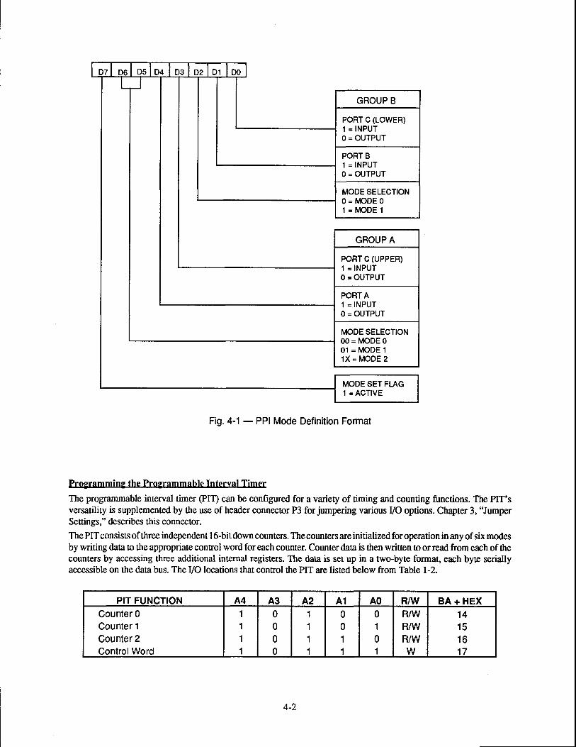
The PPI ports can be operated in one of three modes. The mode of operation and the signal direction of each port (inputor output) are controlled by an eight-bit control word written to an internal regisler. Two bits define the mode selection:mode 0, mode 1, or mode 2. Four bits configure the I/O direction: one bit to control PAO-PA7, one bit o control PBG'PB7, one bit o control PCO-PC3, and one bit to control PC4-PC7. Port C is divided into two four-bit fields so that it canprovide status and control for port A if desired in your application. The control word is defined in Figure 4-1.
The PPI is configured by writing a control word to it's intemal consol register. Upon power-up, all ports arc configuredas mode 0 inputs. The PPI is wriuen to during board initialization so that port B is set up as a mode 0 ouput to configureit for channel selection and gain control functions. Chapter L, "Initializing Your AD2000," describes this procedure.
Because the PPI can be configured for a wide range of operating modes and programming requirements, it is heavilydependent on conectly understanding how to use the proper control byte to configure the PPI for your application. Thedemo disk includes example pro$ams that show how to select the common operating modes. Reading the source codeis highly recommended.
For more information about the operation of the PPI, see the data sheet included in Appendix C.
4-L
D7 D6 D 5 l D 4 l D 3 l D 2 l D 1 l D 0
IGROUP B
PORT C (LOWER)I = TNPUT0 = OUTPUT
PORT B1 = INPUT0 = oUTPUT
MODE SELECTION0 = lvlODE 01 = [4ODE 1
GROUP A
PORT C (UPPER)1 = INPUTO = OUTPUT
PORTA1 = INPUTO = OUTPUT
MODE SELECTION00 = MODE 001 = MODE 1lX = I/IODE 2
MODE SET FI.AG1 = ACTIVE
Fig.4-1 - PPI Mode Definition Format
Programming the Programmable Interval Timer
The programmable interval timer @IQ can be configured for a variety of timing and counting functions. The PIT'sversatility is supplemented by the use of header connector P3 for jumpering various I/O options. Chapter 3, "JumperSettings," describes this connector.
ThePlTconsistsof threeindependent l6-bitdown counters. Thecountersareinitializedforoperationinanyof six modesby writing data to the appropriate control word for each counter. Counter data is then written to or read from each of thecounters by accessing three additional internal registers. The data is set up in a two-byte format, each byte seriallyaccessible on the data bus. The I/O locations that control the PIT arc listed below from Table 1-2.
PIT FUNCTION A4 A3 A2 A1 AO R/W BA + HEXCounter 0Counter 1Counter 2ControlWord
1111
0000
1111
0011
0101
R/WR/WR/WW
14151617
4-Z

Your specific requirements will determine how the individual timer/counters should be conhgured. The data sheetincluded in Appendix C provides the information required to control the pIT.
The software included on the demo disk shows example programs for controlling some of the PIT operating modes. Inaddition, some typical applications are presented in the programmable interval timer application notes in Appendix D.Included are examples requiring two or more couniers to be cascaded.The signals generated by the OUT pins for any of the counters may be connected to one of the PC's intemrpt channelsusing jumpers installed at connectorP5. Refer to the "Hardware Intemrpts" section below for more information on usingthe OUT signals to generate intemrpts.
Hardware Interrupts
Three jumper connectors, P4, P5, and P7, are provided on the AD2000 to enable intemrpts generated by the A/Dconverter, thePIT, thePPI, andan external sourceto thePC's intemrptchannels IRQ2 through IRQ7. Chapter 3, "JumperSettings," explains how these header connectors can be configured.Before you attempt to use interrupts, be sure you are familiar with ttre procedure for initializing the intemrpt vectors andthe PC's interupt controller, and seuing up the intemrpt handling routines. Reference I in Appendix E provides a gooddescription of the PC's system intemrpts.
A"/D Converter End-of-Convert (EOC) Signal
TheA/DconverterEOC signalcanbeusedtogenerateanintemrpttothePC. Anintemrptwilloccur(throughtheselectedinterrupt channel) to indicate a conversion is complete approximately 20 microseconds after the conversion is initiated.The EOC signal is inverted before being applied to the intemrpt channel. It makes a low-to-high ransition at thecompletionofeachconversioncycle,andremainshighuntilanotherconversionisinitiated. ThetimingoftheEOCsignalis shown in Figure 2-2,Chapter 2.
PPI Interrupts
ThePPIINTRA (PC3) intenuptgeneratedinPPl mode l andmode2operationcanbejumperedtoanyof thePC intemrptchannels IRQ2 through IRQ7. The timing of this intemrpt is shown on the PPI data sheet included in Appendix C.The PPI intemtpt must be enabled by writing a "1" to the INI|E mask bil of the PPI as described in the data sheet under"Intenupt, Control Functions." The INTE mask bit is disabled during power-up reset and whenever the PPI mode ischanged.
PIT Interrupts
One of ttre OUT0, OUTI, or OUT2 signals generated by the PIT can be jumpered to a PC intemrpt channel usingconnector P5.
When using a PIT OUT signal as an intemrpt" you must be very careful to ensure that the PC system's programmableinterrupt controller @IC) is properly configured to ignore intemrpts on the selected intemrpt channel immediately afterpower-up. This is necessary because the PIT must first be initialized to define the desired mode(s) of operation. Priorto initialization, the mode, count, and output of all counters are undefined. If the system interrupts are not disabled, thecounter outputs may cause erratic system behavior.
4-3

44

CHAPTER 5
CALIBRATION PROCEDURES


This chapter contains calibration procedures for the A/D converter input voltage range and the A/D converter gain. Theoffset and full-scale performance of the AD2000 A/D converter is factory-calibrated according to the specifications thatwere given when your order was placed. The gain circuitry is also factory-calibrated before the board is shipped. Thefollowing procedure allows you to quickly verify the accuncy of these circuits. This procedure should be doneapproximately every six months, whenever inaccurate readings are suspected, or whenever tle voltage range is changed.Calibration is performed with a properly configured AD2000 installed in the PC. Apply power to the computer and allowthe AD2,000 circuitry to stabilize for 15 minutes.
Required Equipment
The following equipment is required for calibration:. hecision Voltage Source: 0 to +10 volts. Digital Voltmeter: 5-U2 Ctrgit. Small Screwdriver (for aimpot adjustment)
Figure 5- I shows the board layout. The trimpots referenced in the following procedures are grouped in the upper left areaof the board.
Fig. 5-1 - AD2000 Board Layout
A/D Calibration
During this procedure, connections must be made to some of the analog inpus on external I/O connector P8, availableat the rear panel of the computer. The pin assignments for this connector are given in Table B-2, Appendix B.
Two adjusrnents are necessary to completely calibrate the A/D converter for unipolar or bipolar operation. These affectthe offset and full-scale performance of the AD2000 circuiry. Both calibration steps are performed using trimpots TR5and TR6 or TR6 and TR7. Trimpot TR5 or TR7 is used !o zero the offset error of the A,/I) converter and trimpot TR6is used for full-scale adjustment. In the following procedure, use analog input channel 1 and set it for a gain of 1. This
5-r

is accomplished by writing all zeroes to I/O address location BA + l. Be certain ttrat position 4 of switch 51 is set forthe desired polarity and the jumper on connector P9 is set for l0V.
Unipolar Calibration
Two adjustments are necessary to calibrate the A/D converter for the unipolar voltage range of 0 to + l0 volts, one foroffset and one for full scale. To adjust the offset, a very low analog input voltage, shown under the "Offset" heading inthe following table, is connected to the channel I input of the multiplexer @8-1). The ground reference of this signalshould be connected to P8-2. While continuously displaying 12-bit A/D conversions, adjust TR7 until the AID dataflickers between the two values listed in the table under "Offset."
After the offset adjustment is made, TR6 is used o adjust the full-scale value. While the full-scale input voltage listedin the table is not the actual full-scale voltage for an ideal 0 to +10 volt range, it is ttre maximum voltage at which theA/D conversion is guaranteed o be linear. Any value above this voltage may not be linear and thus may adversely affectcalibration. After connecting the full-scale voltage listed in the table to the channel 1 input, adjust TR6 until the dataflickers between the two values in the able under "Full Scale."
Unipolar Calibration(0 to +10 volts ranqe)
Offset (TRn Full Scale (TR6)
Inout Volaee +1.22070 millivolrs +9.49829 volrsA/D Data 0000 0000 0000
00m m00 00011111 m l100101111 0011 0011
Bipolar Calibration
Whether you are selecting the bipolar input voltage range of -5 to +5 volts or - l0 to + 10 vols, the following calibrationprocedure can only be performed with the board configured for a -5 to +5 volt input voltage range. This means that thejumperon headerconnectorP9 mustbeinstalledacross the l0Vpins.If youareusing0re -10 to+10 voltrange,repositionthe jumper on P9 across the 20V pins after you perform the calibration procedures below.
Two adjustments arc necessary o calibrate the A/D converter for bipolar voltage ranges, one for offset and one for fullscale. To adjust the offset" connect the voltage shown under tle "Offset" heading in the table below to the channel I inputof the multiplexer. While continuously displaying l2-bit AID conversions, adjust TR5 until the daa flickers betweenthe two values listed in the table under "Offset." Next, connect the full-scale voltage listed in the cable to the channel Iinput and adjust TR6 until the data flickers between the two values in the table under "Full Scale."
Bipolar Calibration(-5 to +5 volts or -10 to +10 volts ranse)
Offset ffR5) FuIl Scale (TR6)
Inout Voltaee 4.99878 vols +4.99634 voltsA/DDaa 0m 0000 0000
0000 0000 00011 1 1 1 l l 1 1 l l 1 01 1 1 1 1 1 1 1 1 1 1 1
Table 5- 1 provides a reference for the ideal input voltage for the A7D converter for each bit weight in each voltage range.This table shows ilre ideal full-scale (all ones) value in the first line and decrements by one bit weight each line thereafter.Note that these values are for l2-bit AID conversions, and are not valid when using the converter to perform more rapideight-bit conversions. Note that the voltage values in the table are in millivols.
5-2

Table 5-l - A/D Converter Blt Welqhts
A/D RitWeishtfdeal Innut Voltace (millivolts)
+5 Volts +10 Volts 0 to +10 Volts
4095 (Full-Scale)2M8rgu5t2256r28&3216842I0
+4997.60000.0
-2500.0-3750.04375.04687.54M3.8492r.949ffi.94980.549n.24995.t4997.6-sO(n.0
+9995.10000.0-5000.0-7500.0-8750.0-9375.0-9687.5-9843.8-992r.9-99ffi.9-9980.5-99W.2-9995.r
-10m0.0
+9997.6+5000.0+2500.0+1250.0+625.00+312.50+156.250+78.125+39.053+19.5313+9.7656+4.8828+2.4/.140.0000
Gain Circuitry Calibration
Four rimpots,TRl through TR4, are used to adjustthegain circuitry, one foreach of the gains 2,4,8, and 16. To calibratethis circuiry, apply an input voltage of +39.063 miltvolrs o the input of channel 1. Next, by writing the corrc,ct wordto ttre BA +1 I/O location, set the gain to 2 and adjust trimpot TRl to obtain the 12-bit A/D converter output for yourboard's voltage range, as listed in Table 5-2. Then, repeat this procedure for each of the remaining three gain settings,adjusting the appropriate rimpot until achieving the correct value listed in the table.
Table 5-2 - A/D Converter Readinqs for Galn Callbrallon
Gain Trimpot
Inout Voltaee Range+5 Volts +10 Volts 0 to +10 Volts
248l6
TRlTR2TR3TR4
1000 0010 00001000 0100 00001000 1000000010010000m00
1000 0001 00001000 0010 00001000 0100 00001000 1000 0000
0000 0010 00000000 01m 00000000 1000 00000001 0000 0000
5-3

54

APPENDIX A
AD2OOO SPECIFICATIONS


(Typical N25"C)
Interface:
Analog Inputs:
A"/D Converter:
Counter/Timer:
Digital UO Lines:
Miscellaneous I/Os:
Power Requirements:
VO Connectors:
AD2OOO SPECIFICATIONS
IBM PC/XT/AT compatibleJumper-selectable base address, VO mappedJumper-selectable intemrpts
8 differential or 16 single-ended inputs, switch-selectableInput impedance, each channel ..... >10 megohmsGains, software selectable 1,2,4,8, or 16Gain error 0.5Vo typ, lvo maxInput options: l0-volt range* (Option 1).......... Bipolar +5V
Guaranteed Linearity ...............+5Vl0-volt range* (Option 2) .......... Unipolar 0 to +l0VGuaranteed Linearity ............... 0 to +9.5V
20-volt range* (Option 3).......... Bipolar +10 VGuaranteed Linearity ...............19.5V
Range.......... .......... Jumper-selectablePolarity Switch-selectable
Settling time ............ .3 psec maxCommon mode input voltage ........+10VOvervoltage protection t35 Vdc*Erratic readings can occur beyond specified input voltage rilnges.
Type............ Successive approximationResolution: 10-voltrange ........lzbitsQ.44 mVlbit)
2O-volt range ........ 12 birs (4.88 mVlbit)Chip-selectable conversion speed: Option 0 .... 20 Usec typ,25 trec max
Option | .... 12 psec qrp, 15 psec maxOption 2 ....8 psec typ,9 psec max
Linearity tl bit typSample-and-hold acquisition time .6 Fsec maxThroughput ...............38 kHz
Three l6-bit, 8 MHz down counters
16 TTL/CMOS-compatible
+12V, +5V, PC bus-sourcedGround, PC bus-sourcedOne extemal intemrpt input
+5 Volts 260 mA+12 Volts 30 mA-12 Volts 35 mA
Two 40-pin box headers (one dedicated to analog signals only)All 80 signals exit through one rear panel slot in the PC
A-l

Size:
Operating temperature 0 to +70oCStorage temperature. . -40 to +85"CHumidity..... 0 tn %)Vo non-condensing
Height .. 3.875" (99 mm)Width.......... 5.50" (140 mm)
A-2

APPENDIX B
CONNECTOR PIN ASSIGNMENTS


CONNECTOR PIN ASSIGNMENTS
Table B-l-Mating External IiO Connectors for P8 and P15
Connector No. Manufacturer Part Number
P8P15
3MMil c-83503
yr1-7M0M8?sOit-os
Table B-2-P8 Connector Pin Assignments
Pin No. Signal Name
DIFF / SE
Pin No. Signal Name
IJ
57911r315T7192r232527293 lJ J
35J I
39
AINI+ / AIN1AINI- / AIN9AIN2+/ AIN2ArN2- / AIN10AIN3+ / AIN3AIN3- / AINI1AIN4+ / AIN4AIN4- / AIN12AIN5+ / AIN5AINs- / AIN13AIN6+ / AIN6AIN6- / AINI4AINT+ / AINTAINT- / AINI5AIN8+ / AIN8AIN8. / AINI6
N.C.N.C.
+12 VOLTS.12 VOLTS
2468l0t2t4r6l 82022242628303234363840
GNDGNDGNDGNDGNDGNDGNDGNDGNDGNDGNDGNDGNDGNDGNDGNDGNDGNDGNDGND
B-1

Table B-3-PI"5 Connector Pin Assignments
Pin No. Signal Name Pin No. Signal Name
I3579111315I7192l232527293133353739
GNDPA7PA5PA3PAlGNDPC7PC5PC3PC1GND
EXTCLKOCLKOUTO/CLKOUTG
EXTCLKlCLKOI-]"TI /CLKOUTI.
EXTCLK2CLKOUT2 / CLKOUT2-
+5 VOLTSGND
+12 VOLTS
2468l0t2t4l6l82022242628303234363840
EXTINTPA6PA4PA2PAOGNDPC6PC4PC2PC0GND
EXTGATEOGND
EXTGATElGND
EXTGATE2GND
+5 VOLTSGND
-12 VOLTS
B-2

APPBNDIX C
COMPONENT DATA SHEETS


Intel 82C55A Programmable Peripheral lnterfaceData Sheet Reprint

intel'82C55A
I Control Word Read-Back Capability
I Direct Bit Set/Reset CaPabilitY
. 2.5 mA DC Drive Capablllty on all l/OPort OutPuts
r Available In 40-Pin DIP and 44'Pin PLCC
r Available in EXPRESS- Standard Temperature Range- Extended Temperature Range
The Intel 82C55A is a high-performance, CHMOS version of the industry standard 8255A general purposeprogrammable l/O device which is designed for use with all lntel and most other microprocessors. lt provides
Zq ltO pins which may be individually programmed in 2 groups ot 12 and used in 3 major modes of operation.The 82C55A is pin compatible with the NMOS 8255A and 8255A'5.
ln MODE 0, each group of 12 llo pins may be programmed in sets ol 4 and 8 to be inputs or outputs. InMODE 1, each group may be programmed to have 8 lines of input or output. 3 of the remaining 4 pins are usedfor handshaking and interrupt control signals. MODE 2 is a strobed bi-directional bus configuration.
The 82C55A is fabricated on Intel's advanced CHMOS lll technology which provides low power consumptionwith performance equal to or greater than the equivalent NMOS product. The 82C55A is available in 40-pinDIP and 44-pin plastic teaded chip carrier (PLCC) packages.
ltsET
0o
D '
NC
0a
03
o5
o7
CHMOS PROGRAMMABLE PERIPHERAL INTERFACE
I Compatible with all Intel and MostOther Microprocessors
r High Speed, "Zero Wait State"Operation with 8 MHz 8086/88 and80186/188
a 24 Programmable l/O Plns
t Low Power CHMOS
r Completely TTL ComPatible
t e I r I r I I r i t t t
csdD
Al
N
7C'
rcPo6rc5PAl
PPFEE9F iEFE
I
l 0
I t
l 4
t 5
t 6
t t
}EClaB ' IG
!
6
231256-1
Flgure 1.82C55A Block Diagram
231256-2
Figure 2.82C55A PinoutDiagrams are lor pin relerence only. Packagesiz€s ar€ not to scale.
S.ptcmbcr 19t7Ordcr llumbcn 23 | 2564o.43-124
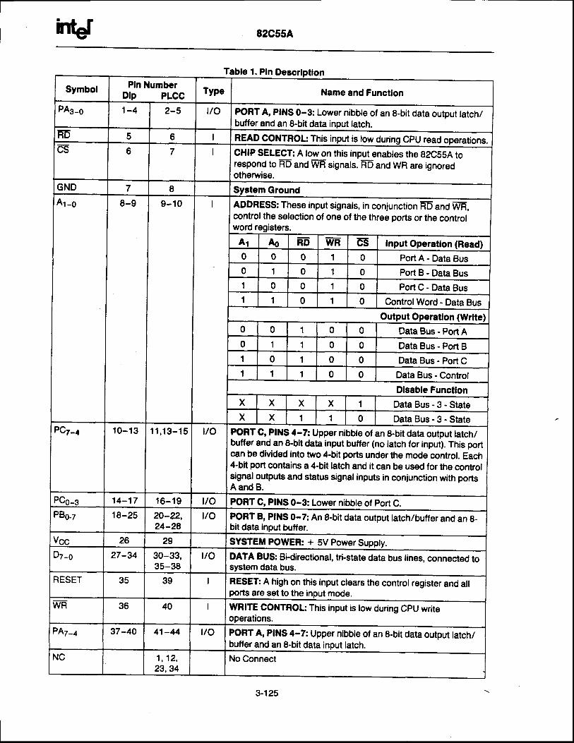
82C55A
Table 1. Pln
Symbol Pln NumberDlp PLCC Type Name and Function
PAg-o 1-4 2-5 t/o POFT A, PINS 0-3: Lower nibble of an 8-bit data output latch/butfer and an 8-bit data input latch.
m 5 6 I READ CONTROL: This input is low during CpU read op€rations.m 6 7 I CHIP SELECT: A tow on this input enables the 82C5SA torespond to RE and WFI signals. ffi and WR are ignoredotherwise.
GND 7 8 System GroundAr-o 8-9 9 - 1 0 ADDRESS: These input signals, in conjunction F-D and WF[,
control the selection of one of the three ports or the controlword registers.
A1 As m wF' cs Input Operatlon (Read)0 0 0 1 0 PortA-DataBus0 1 0 1 0 PortB-DataBus1 0 0 1 0 PortC-DataBusI 1 0 1 0 ControlWord - Data Bus
Output Operatlon (Wrlte)0 0 1 0 0 Data Bus - Port A0 1 1 0 0 Data Bus - Port B1 0 1 0 0 Dala Bus - Port G1 1 1 0 0 Data Bus - Control
Disable Functlonx X X X 1 DataBus-3-StateX X 1 1 0 DataBus-3-State
Pcz-l 1 0 - 1 3 1 1 . 1 3 - 1 5 vo PORT C, PINS 4-7: Upper nibble of an 8-bit data output latch/butfer and an 8-bit data input butfer (no latch for input). This portcan be divided into two 4-bit ports under the mode control. Each4-bit port contains a 4-bit latch and it can be used for the controlsignal outputs and status signalinputs in conjunction with portsA and B.
PCo-g 14-17 1 6 - 1 9 t/o PORT C, PINS 0-3: Lower nibbte of port C.PBo-z 1 8-25 20-22,
24-28uo PORT B, PINS 0-7: An 8-bit data output latch/butfer and an g-
bit data input butfer.Vee 26 29 SYSTEM POWER: * 5V Power Suppty.Dz-o 27-34 30-33,
35-38t/o DATA BUS: Bi-directional, tri-state data bus lines, connected to
system data bus.RESET 35 39 RESET: A high on this input clears the controt register and all
ports are set to the input mode.wF' 36 40 WRITE CONTROI,.: This input is tow during CpU write
operations.PAz-a 37-40 41 -44 t lo PORT A, PINS 4-7: Upper nibble ot an 8-bit data output tatch/
butfer and an 8-bit data input latch.NC 1 , 1 2 ,
23,34No Connect
3-125
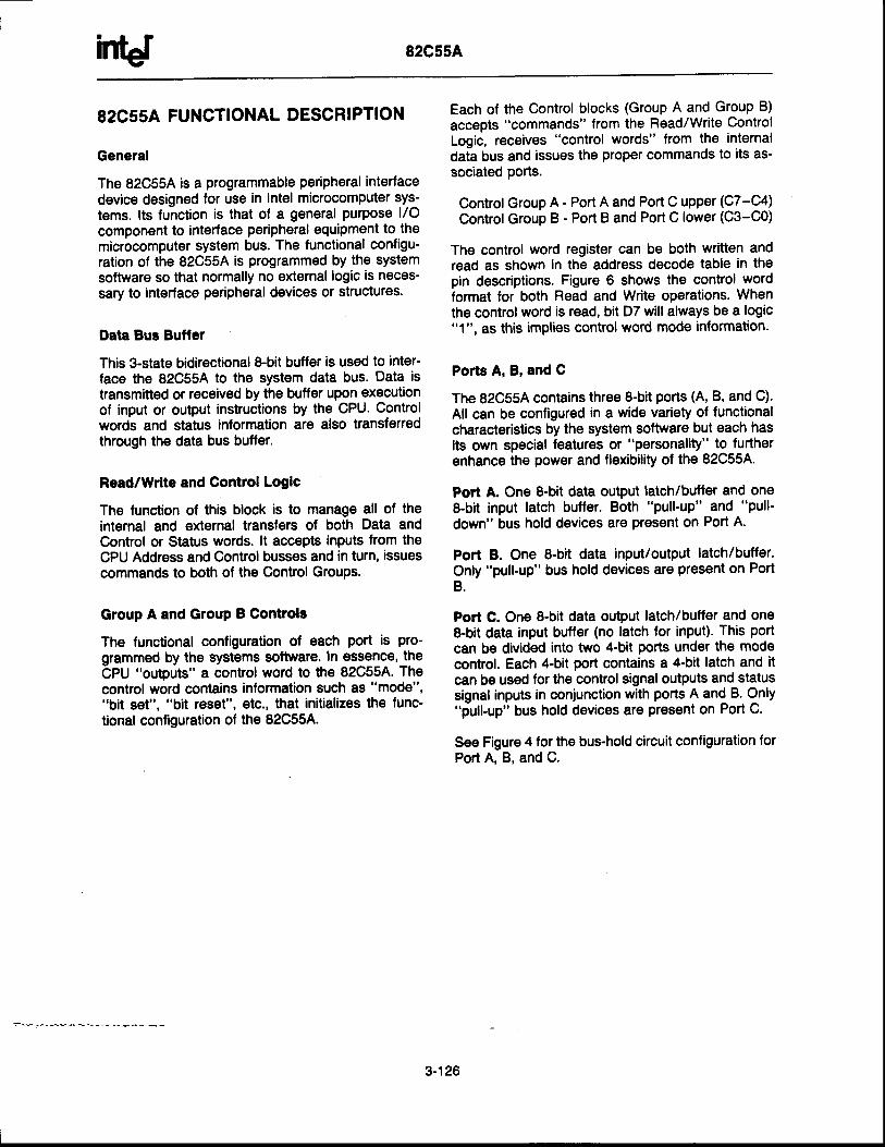
intet 82C5sA
82C55A FUNCTIONAL DESCRIPTION
General
The 82C55A is a programmable peripheral interfacedevice designed for use in Intel microcomputer sys-tems. lts function is that of a general purpose l/Ocomponent to interface peripheral equipment to themicrocomputer system bus. The functional configu'ration of the 82C55A is programmed by the systemsoftware so that normally no external logic is neces-sary to interface peripheral devices or structures.
Data Bue Buffer
This 3-state bidirectionalS-bit butfer is used to inter'face the 82C55A to the system data bus' Data istransmitted or received by the buffer upon executionof input or output instructions by the CPU. Gontrolwords and status information are also transferredthrough the data bus butfer.
Read/Wrlte and Control Loglc
The function of this block is to manage all of theinternal and external transfers of both Data andGontrol or Status words. lt accepts inputs from theCPU Address and Controlbusses and in turn, issuescommands to both of the Control Groups.
Group A and Group B Controlg
The functional configuration of each port is pro-grammed by the systems sottware. In ossence, theOPU "outputs" a control word to the 82C55A. Thecontrol word contains information such as "mode","bit set", "bit r€sot", etc., that initializes lhe func'tional configuration of the 82C55A.
Each of the Control blocks (Group A and Group B)accepts "commands" from the Read/Write ControlLogic, receives "control words" from the internaldata bus and issues the proper commands to its as-sociated ports.
Control Group A - Port A and Port C upper {C7-O4lControlGroup B - Port B and Port C lower (C3-C0)
The control word register can be both written andread as shown in the address decode table in thepin descriptions. Figure 6 shows the control wordformat for both Read and Write operations. Whenthe controlword is read, bit D7 will always be a logic"1", as this implies control word mode information.
Ports A, B, and C
The 82C55A contains three 8-bit ports (A, B, and C).All can be configured in a wide variety of functionalcharacteristics by the system software but each hasits own special features or "personality" to furtherenhance the power and flexibility of the 82C55A.
Port A. One 8-bit data output latch/butter and oneI'bit input latch butfer. Both "pull-up" and "pull'down" bus hold devices are present on Port A.
Port B. One 8-bit data input/output latch/butfer'Only "pull-up" bus hold devices are present on PortB.
Port C. One 8-bit data output latch/buffer and one8-bit data input bufler (no latch for input). This portcan be divided into two 4-bit ports under the modecontrol. Each 4-bit port contains a 4'bit latch and itcan be used for the control signal outputs and statussignal inputs in conjunction with ports A and B. Only"pull-up" bus hold devices are present on Port C'
See Figure 4 for th€ bus-hold circuit configuration forPort A, B, and C.
3-126
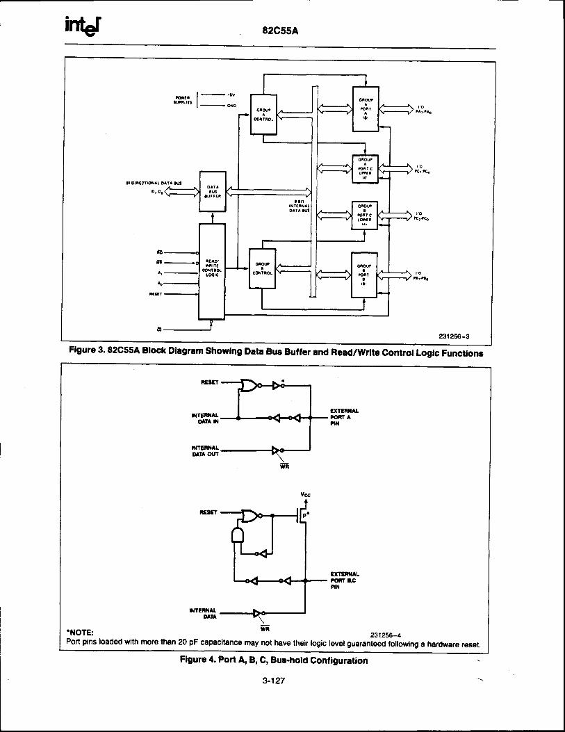
intef 82C55A
mil
te&l
231256-3
Flgure 3.82C55A Block Dlagram Showlng Data Bua Buffer and Read/Wrlte Control Logtc Funcilong
I'{TEFI{ALoATA ll{
IiITgRNALo^t (xrr
SITEFIIALOATA
'NOTE: wn
Port pins loecled with more than 20 pF capacitanc€ may nol have their logic231256-4
level guaranteed following a hardwaro reset.
Flgure 4. Port A, B, C, Bus-hold Configuration
3-127

intef 82C55A
82C55A OPERATIONAL DESCRIPTION
Mode Selectlon
There are three basic modes of operation that canbe selected by the system sottware:
Mode 0 - Basic input/outPutMode 1 - Strobed InPut/outPutMode 2 - Bi-directional Bus
When the reset input goes "high" all ports will be setto the input mode with all 24 port lines held at a logic"one" level by the internal bus hold devices (seeFigure 4 Note). After the reset is removsd the82C55A can remain in the input mode with no addi'tional initialization required. This eliminates the needfor pullup or pulldown devices in "all CMOS" de'signs. During the execution of the system program'any of the other modes may be selected by using asingle output instruction. This allows a single82C55A to service a variety of peripheral deviceswith a simple software maintenance routine.
The modes for Port A and Port B can be separatelydefined, while Port C is divided into two portions asrequired by the Port A and Port B definitions. All ofthe output registers, including the status flip'flops,will be reset whenever the mode is changed. Modesmay be combined so that their functional definitioncan be "tailored" to almost any l/O structure. Forinstance; Group B can be programmed in Mode 0 tomonitor simple switch closings or display computa'tional results, Group A could be programmed inMode 1 to monitor a keyboard or tape reader on aninterrupt-driven basis.
:.::,- F.-.r\r- - -.-.Iigli" 5' Basic Mode Definltions and Bus
lnterface
231256-5
Flgure 6. Mode Deflnltlon Format
The mode definitions and possible mode combina'tions may seem confusing at first but after a cursoryreview of the complete device operation a simple,logical l/O approach will surface. The design of the82b55A has taken into account things such as etfi'cient PC board layout, control signal definition vs PClayout and complete functional flexibility to supportalmost any peripheral device with no extemal logic.Such design repr€sents the maximum use of theavailable pins.
Slngle Blt Set/Reget Feature
Any of the eight bits of Port C can be Set or Resetusing a single OUTput instruction. This feature re'duces sotware requirements in Gontrol'based appli'cations.
When Port C is being used as status/controllor PortA or B, these bits can be set or reset by using the BitSet/Reset operation iust as if they were data outputports.
3-128
coartFoL wonD
o, or D6 oa o2 Dl oo
J
/ oiolr! \
foRT c tKncnll. lxPul0.oUlruT
foel 3t . lt{PUT0. OUttUT
XODE EELEC'IOII0. li{)OC 0I . l,lOOE I
/ oFott ^ \
foit c rtttcil! .lt{'uf0. OUTruT
tont aI . ItitttT0.OutruT
X(DE 3:LECTlOltlO. rrcOl0O! . |IODE ttX . r |OE 2
TODE ECT FLA6l. ASTIVE
231256-6
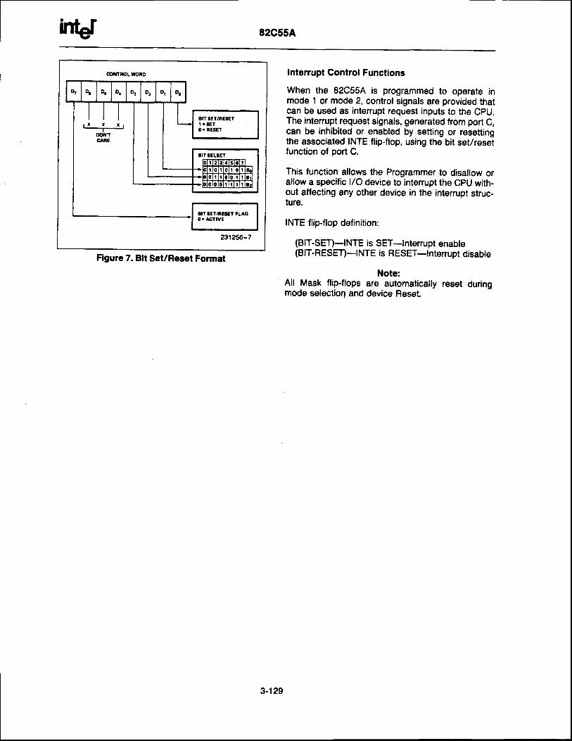
intef 82C55A
oot{taot wotD
231256-7
Flgure 7. Blt Set/Reset Format
Interrupt Control Functlons
When the 82C55A is programmed to operate inmode 1 or mode 2, control signals are provided thatcan be used as interrupt request inputs to the CPU.The interrupt requ€st signals, generated from port C,can be inhibited or enabled by setting or resettingthe associated INTE flip-flop, using the bit set/resettunction of port G.
This function allows the Programmer to disallow orallow a specific l/O device to intenupt the CPU with-out atfecting any other device in the interrupt struc-ture.
fNTE flip-flop definition:
(BIT-SETFINTE is SET-Interrupt enabte(BIT-RESET)-INTE is RESET-tntenupt disabte
Note:All Mask flip-flops are automatically reset duringmode selection and device Reset.
3-129
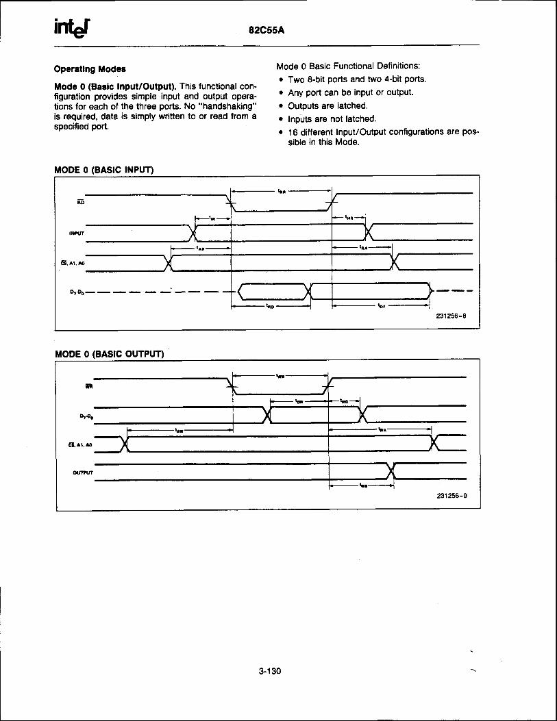
intet
operailng Modes Mode 0 Basic Functional Definitions:
Mode 0 (Bastc Input/output). This functionat con- : l:o -t^o't ports and two 4-bit ports'
figuration providei simple'input ano output opera- o AnY port can be input or output'tions for each of the three ports. No "handshaking" r Outputs are latched.is required, data is simply written to or read from a . Inpirts are not latched.specified port' o 16 ditferent Input/output configurations are pos-
sible in this Mode.
MODE 0 (BASTC INPUT)
231256-8
MODE o (BASTC OUTPUT)
231256-9
3-1 30
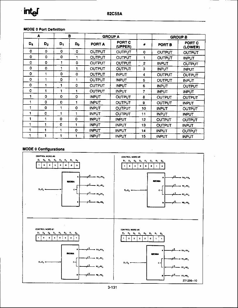
A B GROUP A GROUP BDa D3 D1 D6 PORT A PORT C
(UPPER) # PORT B PORT CGOWER)
0 0 0 0 OUTPUT OUTPUT 0 OUTPUT OUTPUT0 0 0 1 OUTPUT OUTPUT 1 OUTPUT INPUT0 0 1 0 OUTPUT OUTPUT 2 INPUT OUTPUT0 0 1 1 OUTPUT OUTPUT 3 INPUT INPUT0 1 0 0 OUTPUT INPUT 4 OUTPUT OUTPUT0 1 0 1 OUTPUT INPUT 5 OUTPUT INPUT0 1 1 0 OUTPUT INPUT 6 INPUT OUTPUT0 1 1 1 OUTPUT INPUT 7 INPUT INPUT1 0 0 0 INPUT OUTPUT 8 OUTPUT OUTPUT1 0 0 1 INPUT OUTPUT I OUTPUT INPUT1 0 1 0 INPUT OUTPUT 10 INPUT OUTPUT1 0 1 1 INPUT OUTPUT 1 1 INPUT INPUT1 1 0 0 INPUT INPUT 1 2 OUTPUT OUTPUT1 1 0 1 INPUT INPUT 1 3 OUTPUT INPUT1 1 1 0 INPUT INPUT 1 4 INPUT OUTPUT1 1 1 1 INPUT INPUT 1 5 INPUT INPUT
MODE 0 Gonliguratlons
ooNrnot i,oio r0 GOfT|TROL WORO a2
coflTFor Yronotr
D, Da Oi O. O: Dr Or
3-131

o, o. 05 o. ot o, or Do
cor|'iot roFD a6
coirrRol rroiD r
coilnot tono aT
o, oc or o. o! D, or Do
coxtRoL fi)ioae
c(xttoL xoRo rtoo, oa o, D. ot Dr Dr oo
oot{lRol troio art
0 0 0 I
I o 0 0 0 0
3-132
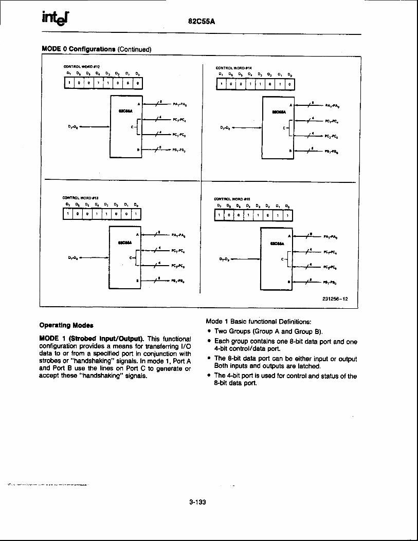
IIODE 0 ConllguraUona (Continued)
ooxttol irotD tt!D r % D r D r D l D 2 D r O o
r l 0 l 0 l r l r l 0 l 0 l r
co,llnol woRortaDr 03 03 O. Dr Or Or Oo
r l 0 l 0 l l l l l 0 l t l 0
oofl?tol totD att
o, or Dr O. D: Dz Dr Do
ffi
o, oa or o. Dt D: Or Oo
inbf 82C55A
Opcretlng todcr
ilODE 1 (Strobed Input/Output). This functionalconfiguration provides a means for transferring l/Odata to or from a specified port in coniunction withstrobes or "handshaking" signals. In mode 1, Port Aand Port B use lhe lines on Port C to generate oraccept these "handshaking" signals.
Mode 1 Basic functional Definitions:o Two Groups (Group A and Group B).o Each group contains one 8-bit data port and one
4-bit control/data port.o The 8-bit data port can be either input or output
Both inputs and outputs are latched.r The 4-bit port is used for control and status of the
8-bit data port.
3-133

intef 82C554
Input Control Slgnal Deflnltlon
STE (strobe Input). A "low" on this input loadsdata into the input latch.
IBF (lnput Buffer FullF/F)
A "high" on this output indicates that the data hasbeen loaded into tha input latch; in essence, an ac-knowledgement. IBF is set by STB inpg! being lowand is reset by the rising edge of the RD input.
INTR (lnterrupt Request)
A "high" on this output can be used to interrupt theCPU when an input device is requesting service'INTR is set by the STE is a "ono", IBF is a "on6"and INTE iE a "one". lt is reset by the lalling edge olFT. nris procedure allows an input device to re-quest service from the CPU by simply strobing itsdata into the port.
INTE AControlled by bit set/reset of PCa.INTE BControlled by bit set/reset of PC2.
coiltaol woiD
Dr Dr Or O. D, 02 D! DO
tQ.r
t . ltatt l0. OUttUt
m^
t !F^
|l{tR^
r/o
RD
3ll.
||Fr
ItT\
231256-13
I trtE !
Li- . i
mE r t;oiYll
r - - ' 1I IT?E II r it T - - ,
t _
o, o: Dt Do
Flgure 8. MODE 1 Input
l|t
It
txtt
E
ntr?lc- - -tttfiStal
231256-14
Flgure f. ilODE I (Strobcd InPut)
3-134

intef 82C55A
Output Control Slgnal Deflnltlon
OBF (Output Buffer Fuil F/F). The OEF output witlgo "low" to indicate that the CPU has written dataout to the specified port. The 6EF ptp wiil be set bythe rising edge of the WF input and reset by ERInput being low.
ffi (Acfnowledge Input). A "low" on this inputinforms the 82C55A that the data from Port A or portB has been accepted. In essenc€, a response fromthe peripheral device indicating that it has receivedthe data output by the CPU.
INTR (lnterrupt Request). A "high"'on this outputcan be used to int€nupt the CPU when an outputdevice has accapted data transmitted bv the CpU.INTR is set wh€n ffi is a "one", OgF--is a "one"and INTE is a "one". lt is reset by the falling edge ofwF.
INTE AControlled by bit set/res€t ot pC6.
INTE BControlled by bit set/reset of PC2.
231256-16
Flgure ll.llODE 1 (Strobed Output)
ooirraol roto
cf^
&-x^
ltfTRa
oorniolf,oiD
ilh
ec
rrri|
231256-15
r _ - 1I lillE It a ll - - - J
Flgure 10. MODE I Output
3-13s

int€f 82C55A
Comblnatlons of MODE 1
Port A and Port B cbn be individually defined as input or output in Mode 1 to support a wide variety of strobedl/O applications.
?c.
?c!
fca
Er.r
?srto
?cr
Fcl
,!co
?ar'?\
rc7
fc.
tc!
OONTBOL v,OFD
.rt
|lfr
tNlR!
IOiTA-ISTROIEDINPU?IaoRr I - ls?RoeEo ourrurl
toi? A - tstRoaEDouTPutlroRTs -tsrno6Eorl|rurl
231256-17
Flgure 12. Comblnatlons of MODE 1
Operatlng Modes
ltlODE 2 (Strobed Bidlrectlonal Bus l/O).Thisfunctional configuration provides a means for com'municating with a peripheral device or structure on asingle 8-bit bus for both transmitting and receivingdata (bidirectional bus l/O). "Handshaking" signalsare provided to maintain proper bus flow discipline ina similar manner to MODE 1. Interrupt generationand enable/disable functions are also available.
MODE 2 Basic Functional Definitions:o Used in Group A only.r One 8-bit, bi-directional bus port (Port A) and a 5'
bit control port (Port G).o Both inputs and outputs are latched.o The S-bit control port (Port C) is used foi control
and status for the 8-bit, bi-directional bus port(Port A).
Bldirectional Bus l/O Control Signal Deflnltion
INTR (lnterrupt Request). A high on this output canbe used to interrupt the CPU for input or output oper'ations.
Output Operatlons
6'F (Output Bulter Full). The OBF- output will go"low" lo indicate that the CPU has written data outto port A.
AC-K (lctnowledge). A "low" on this input enablesthe tri-state output butler of Port A to send out thedata. CIherwise, the output butfer willbe in the highimpedance state.
INTE 1 Ohe INTE Flip-Flop Associated wlthO-BF). Controlled by bit set/reset of PC6.
Input Operatlons
SF (Stroue Input). A "low" on this input loadsdata into the input latch.
IBF (lnput Buffer Full F/F). A "high" on this outputindicates that data has been loaded into the inputlatch.
INTE 2 (Ihe INTE Flip-Flop Assoclated wlth IBF).Controlled by bit set/reset of PCa.
3-136

int€f 82C55A
ooiltRot vfoRD
o, D. D! O:
toaY I1 .INArT0 - OUTTUT
GhOT'BNODE0'rrcDt 0I - IrOOE I
231256-18
Flgure 13. MODE ControtWord
oo-^
ffi^
m^
tSFa
tlo
231256-19
Flgure 14. MODE 2
D t^trorc?u to tzctta
rcr
str
tBf
tt it?HtnaLB t s
l l n
oallfHtcftrartial roarc..l
or?a tlolaro|.a ro tgtfircr^r
Figure 15. MODE 2 (Btdtrec$onat)
NOTE:Any sequence qhere wfugcurs before rER, :ld sTEgccurs before HD is permissibte.(INTR : IBF o Niffi. STB-. FD + 6EF.IiIR o [fi r ffi;
3-137
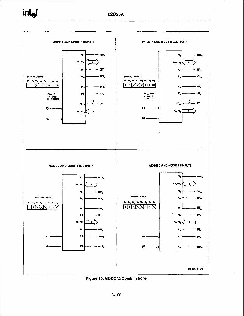
intef 82C55A
oarxTtoL toiD
D r D r Q D . D r D r D t O o
tlri^
6?^
E-q
F-B^
|lF^
rr'o
6-f^
-i^
;fr.
llt^
ilFr
iE-r
tit?hr
MODE 2 AND MODE O (OUTPUTI
MODE 2 AND MOO€ 1 (INPUT}
MOOE 2 AND MOOE O (INPUT}
cf^
7m^
-aT!^
t!t^
r,lt
MOOE 2 ANO MODE I (OUTPUT}
RO
tn
5-r^
E-r^
6^
lttr
4 D r O s D . D t D r O r D o
rcr
tar,t\
rg
q
lc.
q
Er.
tBr+i!
r+.t\
|c?
?cr
fc.
tcr
tt tB!
lcr
fc'
tcr
lc.
tct
tE".tq
fc,
lct
fco
Figure 16. i/IODE 1Z Combinatlons
3-138

intef 82C55A
PAoPArPAzPAgPAaPAsPAoPAz
MODE O
!N OUT
ININININININtNIN
OUTOUTOUTOUTOUTOUTOUTOUT
PBoPBrPBzPBsPBaPBsPBePBz
ININININININININ
OUTOUTOUTOUTOUTOUTOUTOUT
PcoPCrPczPCgPCaPCsPCePCt
ININININININININ
OUTOUTOUTOUTOUTOUTOUTOUT
Mode Deflnltlon Summary
MODE 1
!N OUT
INININININ1NININ
OUTOUTOUTOUTOUTOUTOUTOUT
INININININ1NININ
OUTOUTOUTOUTOUTOUTOUTOUT
INTRslBFssTEsINTR1SfEalBFlvouo
INTRsoBFBAffisINTRIt/ovo
7ffiaoBFA
Speclal Mode Gomblnatlon Conslderatlons
There are several combinations of modes possible.For any combination, som€ or all of the Port C linesars used for control or status. The remaining bits areeither inputs or outputs as defined by a "Set Mode"command.
Durinq a read of Port C, the state of all the Port Clines,ixcept the AOK- and STE lines, will be placedon the data bus. In place of the ACK and STB linestates, flag status will appear on the data bus in thePC2, PC4, and PC6 bit positions as illustrated byFigure 18.
Through a "Write Port C" command, only the Port Cpins programmed as outputs in a Mode 0 group canbe written. No other pins can be atfected by a "WritePort C" command, nor can the int€nupt enable flagsbe accessed. To write to any Port C output pro-grammed as an output in a Mode 1 group or to
MODE OOR MODE 1ONLY
change an interrupt enable flag, the "Set/Reset PortC Bit" command must be used.
With a "Set/Reset Port C Bit" command, any Port Cline programmed as an output (including INTR, IBFanO 6BF) can be written, or an intenupt enable flagcan be either set or reset. Port G lines programmedas inputs, including Iffi and SIB lines, associatedwith Port C are not atlected by a "Set/Reset Port CBit" command. Writinglc the conesponding Port Gbit positions of the ACK and STB lines with the"Set/Reset Port C Bit" command will atfect theGroup A and Group B intenupt enable flags, as illus-trated in Figure 18.
Current Drlve Capablllty
Any output on Port A, B or C can sink or source 2.5mA. This feature allows the 82C$5A to directly driveDarlington type drivers and high-voltage displaysthat require such sink or source cunent.
MODE 2
GROUP A ONLY
€
vot/ol/o
INTR6sfBalBFa
AfKAoEFA
3-139
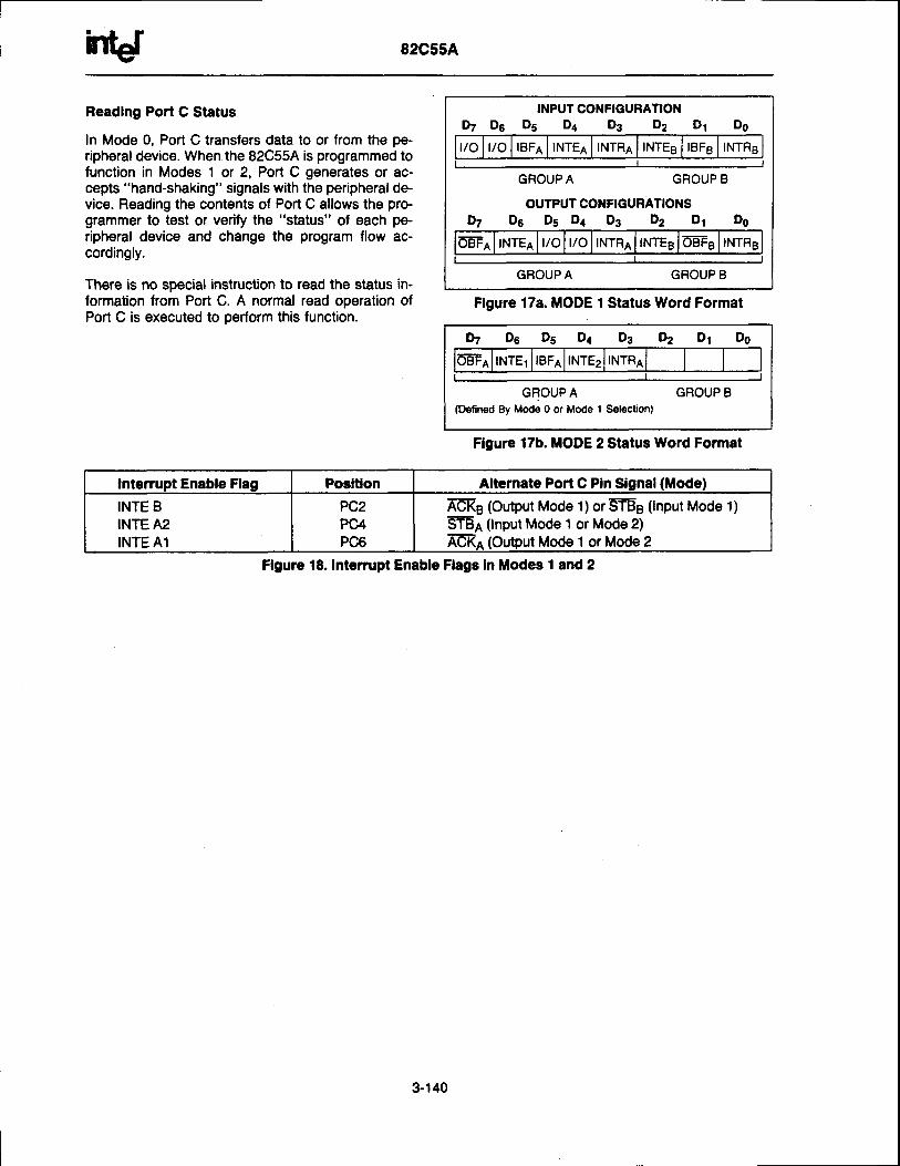
intef 82C55A
Readlng Port C Status
In Mode 0, Port C transfers data to or from the pe-ripheraldevice. When the 82C55A is programmed tofunction in Modes 1 or 2, Port C generates or ac-cepts "hand-shaking" signals with the peripheral de-vice. Reading the contents of Port C allows the pro-grammer to test or verify the "status" of each pe-ripheral device and change the program flow ac-cordingly.
There is no special instruction to read the status in-formation from Port C. A normal read operation ofPort C is executed to oerform this function.
INPUT CONFIGURATIOND7 D5 D5 Da D3 D2 D1 D9
tlolt/Ol IBFA I INTEA I INTRa I INTEB I IBFB I INTRB
GROUPA GROUPB
OUTPUT CONFIGURATIONSD7 D5 D5 Da D3 D2 D1 D6
GROUPA GROUPB
Figure 17a. MODE 1 Status Word Format
D7 D5 D5 Da D3 D2 D1 Dq
GROUPA GROUPB(Defined By Mode 0 or Mode 1 S€l€ction)
Flgure 17b. MODE 2 Status Word Format
lnterruDt Enable Flao Posltlon Alternate Port C Pin Sional(Mode)INTE BINTE A2INTE A1
PC2PC4PC6
Afia (Output Mode 1)orSTBg (lnput Mode 1)STEI (lnput Mode 1 or Mode 2)Affia (Output Mode 1 or Mode 2
Flgure 18. Interrupt Enable Flags In Modes 1 and 2
3-140

intet 82C55A
ABSOLUTE MAXIMUM RATINGS- 'Notice: Slressas above those listed under "Abso-lute Maximum Ratings" may cause permanent dam-
AmbientTemperatureUnderBias....0"Cto + 70'C age to the device. This is a stress rating only andStorage Temperature . . . - 65'C to + 150.C functional operation of the device at these or any
supply Vottage 0.5 to + 8.0V o,!!::,":!-1't,* above those indicated in the opera-tionalsections of this specification is not implied. Ex-
operating Voftage . ' . . + 4V to + 7V posure to absolute maximum rating conditions forVoltage on any lnput. . . .GND-2V to * 6.5V extended periods may atfect device reliability.Voltage on any Output . .GND-0.5V to V66 + 0.5VPower Dissipation . . .1 Watt
D.C. CHARACTERISTICSTA = 0 'Cto70oC,VCC: +5V +10%,GND:0Vf iR: -40 'Cto t85 'CforExtendedTemperture)
Symbol Parameter Mln Max Unlts Test CondltlonsVt lnput Low Voltage -0.5 0.8 V
Vrn lnput High Voltage 2.0 Vcc vVor Output Low Voltage 0.4 V lgL : 2.5 mA
Vox Output High Voltage 3.0Vss - 0.4
VV
loxlox
-2.5 mA-100 pA
I11 Input Leakage Cunent * 1 pA V1N = Vgg to 0V(Note 1)
lopl Output Float Leakage Gunent r10 pA V;1 = Vg6 to 0V(Note 2)
loln Darlington Drive Cunent i 2 .5 (Note 4) mA Ports A, B, CR6: 500oVexl : 1.7V
lpnt Port Hold Low Leakage Cunont +50 +300 pA V9g1 : 1.0VPort A only
lpxn Port Hold High Leakage Cunent -50 -300 pA Vggl = 3.0VPorts A, B, C
lpxuo Port Hold Low Overdrive Cunent -350 pA V9gr1: 0.8V
lpnro Port Hold High Overdrive Gunent +350 pA Vggl : 3.0V
lcc V66 Supply Gunent 10 mA (Note 3)
lccsa V66 Supply Cunent-Standby 10 y"A V66 : 5.5VVrru = VCC or GNDPort Conditionsll llP = Open/High
OIP : Open OnlyWith Data Bus :
High/LowFs: HighReset = Low
Pure Inputs :Low/High
NOTES:1. Pins A1, Ao, tF, WF, FE, Reset.
ts: < __.-.-- - -.?. Data8tlqjfartg-E*-c-._3. Outputs op€n.4. Limit output cunenl to 4.0 mA.
3-14'l

inbr 82C55A
CAPACITANCETA : 25'C, Vcc : GND : 0V
NOTE:5. Sampled not 100o/o tested.
A.C. CHARACTERISTICSTA : 0'to 70oC, Vcc : +5V 110%, GND = 0VTR : -40"C to *85'C for Extended Temperature
BUS PARAMETERS
READ CYCLE
Symbol Parameter Mln Max Unlts Test Condltlons
crH Input Gapacitance 10 pF Unmeasured plnsreturned to GNDfc : 1 MHz(s)
cvo l/O Gapacitance 20 pF
Symbol Parameter 82C554.2 Unlts TeatCondltlonrllfn llax
tan Address Stable Before F-D J 0 ns
tRR Address Hold Time AfterFD f 0 ns
tRn RD Pulse WiOtn 150 nstno Data DelayfromFDJ 120 ns
tor FDT to Daa Fbating 10 75 nstnv Recovery Time between HD/WH 200 ns
WRITE CYCLE
Symbol Parametsr 82C55A-2 Unltr TeetCondltlonrtln iler
taw Address Strable Before WF t 0 nstwn Address Hold Time AfterWR f 20 ns Ports A & B
20 ns Port C
tww W-R Pulse Width 100 ns
tow Data Setup Time Before WR f 100 ns
two Data Hold Time AfterWH T 30 ns Ports A & B
30 ns Port C
g-'t42

intef 82C55A
OTHER TIMINGS
Symbol Parameter 82C55A-2 UnltsCondltlone Test
Mln Max
twe WFI : l toOutput 350 nstrR Peripheral Data Before RD 0 nstxn Peripheral Data After ffi 0 nstnr Affi Pulse Width 200 nstsr STB- Pulse Width 100 nstps Per. Data Belore SfB Hign 20 nstpx Per. Data AfterSTBHigh 50 nstRo Iff i : 0toOuput 't75 nstxo ffi : 1 to Output Float 20 250 nstwog WFi: l toOBF: O 150 nstnog f f i : OtoOBF-: 1 150 nststg SfB=Oto lBF :1 150 nstRra F iD : l t o lBF=O 150 nstnr f f i :O to INTR:O 200 nstsr SfE i : l t o lNTR:1 150 nstnn Af f i : l t o INTR=1 150 nstwr WFI :0 to |NTR:0 200 ns see note 1tnes Reset Pulse Width 500 ns see note 2
1{OTE:1. INTF T may (rccur as early as WF t.2. Pulse width ol initial Reset pulse atter powerminimum.
on must be at l€ast 50 pSec. Subsequent Reset pulses may be SOO ns
3-143
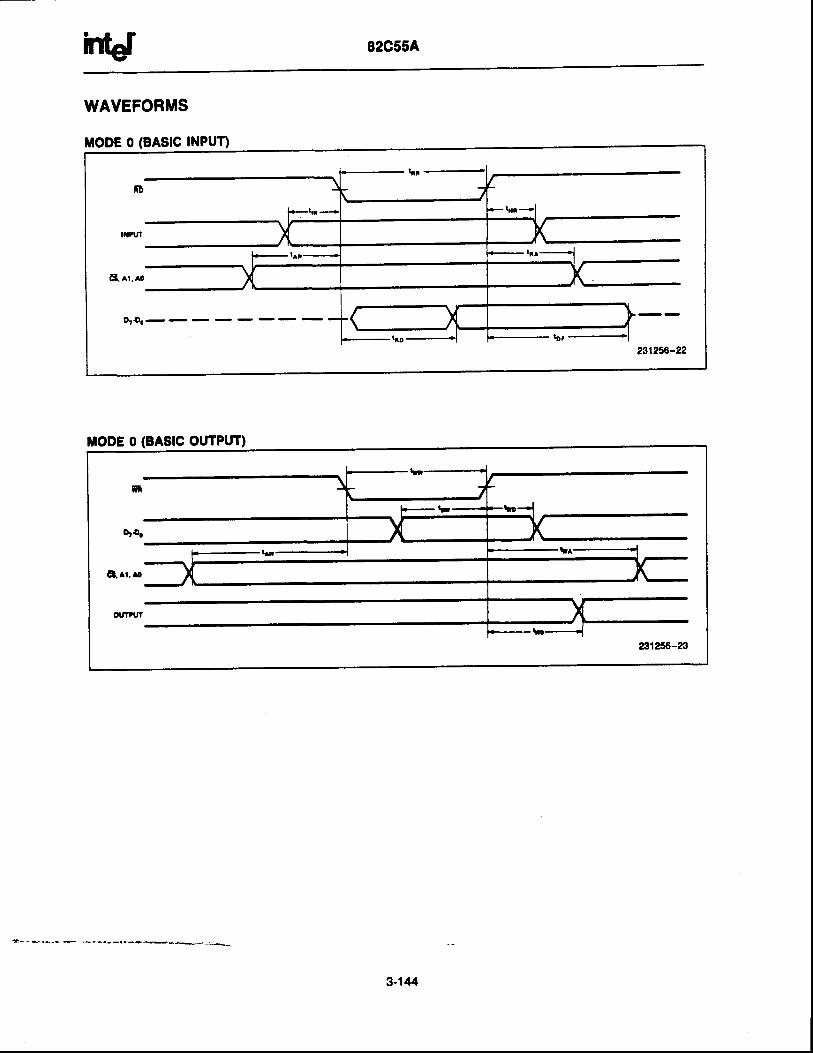
WAVEFORMS
xloDE 0 (BAslc INPUn
291256-22
lroDE o (BAslc ouTPuT)
81256-23
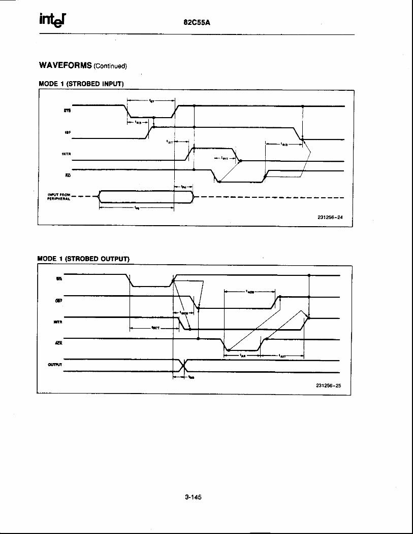
int€t 82C55A
WAVEFORMS (continued)
rroDE 1 (STROBED TNPUT)
m
r!f
|'{in
tFo
i l ?urFnf f___?titi{tnat
2312fi-24
roDE I (STROBED OUTPUT)
m
(5'
tTt
act
qmtt
3-145

intef 82C55A
WAVEFORMS (continued)
rroDE 2 (BIDIRECTIONAL)
DATA iifil2t6 TO rO0
Notc:Anv sequence where WFi occtrs before rcR AND SfE occurs belore FD is permissible.(INTR - IBF o fiIASR. SfB. FD + 6EF. NtIffi o flffi offi1
WRITE TIiIING
231256-27
A.C. TESTING INPUT, OUTPUT WAVEFORII
231256-29
A.C. Teafirg lnputs A?€ Driven At 2.4V For A Logic 1 And 0.45VFor A Logic 0 Timing Measurornents Ate Made At 2.0V For ALooic 1 Ancl 0.8 For A Logic 0.
READ TIIIIING
231236-28
A.C. TESTING LOAD CIRCUIT
= 231256-30
'Vgp ls S€t At Vsrious Voltages During T€sting To GuaranteeTh€ Sp€cification. Cs Includes Jig Capacitance.
3-146


lntel 82C54 Programmable Interval TimerData Sheet Reprint


intel'82C54
I Three Independent 16-blt counters
I Low Power CHMOS- lcc : 10 mA @ 8 MHz Count
frequency
r Completely TTL Compatlble
r Slx Programmable Counter Modes
r Binary or BCD countlng
I Status Read Back Command
I Avallable ln 24-Pln DIP and 28-Pln PLcc
CHMOS PROGRAMMABLE INTERVAL TIMERI Compatlble wlth all Intel and most
other mlcroprocessorsr Hfgh Speed, "Zero Walt State"
Operatlon wlth 8 MHz 8086/88 and80186/188
I Handles Inputs from DC to 8 MHz- 10 MHz tor 82C54-2
r Avallable In EXPRESS- Standard Temperature Range- Extended Temperature Range
The lntel 82C54 is a high-performance, CHMOS version of the industry standard 8254 counter/limer which isdesigned to solve the timing control problems common in microcomputer system design. lt provides threeindependent 16-bit count€rs, each capable of handling clock inputs up to 10 MHz. All modes are softwareprogrammable. The 82C54 is pin compatible with th€ HMOS 8254, and is a superset of the 8253.
Six programmable timer modes allow the 82C54 to be used as an event counter, elapsed time indicator,programmable one-shot, and in many other applications.
The 82C54 is fabricated on lntel's advanced CHMOS lll technology which provides low power consumptionwith performance equal to or greater than the equivalent HMOS product. The 82C54 is available in 24-pin DIPand 28-pin plastic leaded chip carier (PLCC) packages.
231214-3PIASTIC LEADED CHIP CARRIER
5
6
f
I
9
t0
ll
| l r . t 5 t l ' t l
fDmAo
Ar
2312U-1
Flgure 1.82C54 Block Dlagram
O,
Oa
Or
D.
Ot
D,
Dr
Do
ctr 0
our 0OATE O
oro
Ycc
mme5Ar
Ao
ctr 2oul 2c/ttc 2cLt rOA?E 1
OUI r
231244-2Dograms are lor pin ret€r€nc€ only.
Packag€ siz€s are not to scal€.
Ffgure 2.82C54 Pinout
I
?
3
a
5
t,aI
t0
l l
i 2
22Ir,0r ttlt t
3-83Srpt.mb€r 19E9
O?d.r Iumbcn 2gfzffiOS

intef 82C54
Table 1. Pln Deecrlption
SymbolPln Number Type Function
DIP PLCC
Dz-Do 1-8 2-9 t/o Data: Bidirectionaltri-state data bus lines'connected to system data bus.
CLK O I 1 0 I Clock 0: Clock inPut of Counter 0.
OUT O 10 12 o Output 0: Output ol Counter 0.
GATE O 1 1 1 3 I Gate 0: Gate input of Counter 0.
GND 12 1 4 Ground: Power suPPlY connection.
OUT 1 13 1 6 o Out 1: Output of Counter 1
GATE 1 1 4 1 7 I Gate 1: Gate input of Counter 1.
CLK 1 1 5 1 8 I Clock 1: Clock input of Counter 1.
GATE 2 1 6 1 9 I Gate 2: Gate input of Counter 2.
OUT 2 1 7 20 o Out 2: Output of Counter 2.
CLK 2 1 8 21 I Clock 2: Clock input of Counter 2.
Ar' Ao 20-1 I 23-22 Address: Used to select one of the three Countersor the Control Word Register for read or writeoperations. Normally connected to the systemaddress bus.
A1 Ao Selects
0011
0101
Gounter 0Counter 1Counter 2ControlWord Reoister
G 21 24 Ghip Select: A low on this input ena: .. the 82C54to respond to ffi and WFi signals. F' and WFi areionored otheruise.
m 22 26 I Read Control: This input is low during CPU readoperations.
WF 23 27 I Write Control: This input is low during CPU writeooerations.
Vee 24 28 Power: + 5V oower supplv connection.
NC 1 , 1 1 , 1 5 , 2 5 No Connect
FUNCTIONAL DESCRIPTION
General
The 82C54 is a programmable intervaltimer/counterdesigned for use with Intel microcomputer systems.It is a generalpurpose, multi-timing element that canbe treated as an anay of l/O ports in the systemsoftware.
The 82C54 solves one of the most common prob'lems in any microcomPuter system, the generationof accurate time delays under software control. In-stead of setting up timing loops in software, the pro-grammer configures the 82C54 to match his require-ments and programs one of the counters for the de-
sired delay. After the desired delay, the 82C54 willinterrupt the CPU. Sottware overhead is minimal andvariable length delays can easily be accommodated.
Some of the other counter/timer functions commonto microcomputers which can be implemented withthe 82C54 are:
o Realtime clocko Even countero Digital one-shoto Programmable rate generator. Square wave generatoro Binary rate multipliero Gomplex waveform generatoro Complex motor controller
3-84

intef 82C54
Block Dlagram
DATA BUS BUFFER
This 3-state, bi-directional, 8-bit buffer is used to in-terface the 82C54 to the system bus (see Figure 3).
231244-4
Flgure 3. Block Dlagram Showlng Data BusBufler and Read/Wrlte Loglc Functlons
READ/WRITE LOGIC
The Read/Write Logic accepts inputs from the sys-tem bus and generates control signals for the otherfunctional blocks of the 82C54. A1 and Ao selectone of the three counters or the Control Word Regls-ter to be read from/written into. A "low" on the RDinput lells the 82C54 that the CPll_is reading one ofthe counters. A "low" on the WB input tells the82C54 that the CPU is q4!ng either a Control Wordor an initial count. Both RD and WR are qualified byeS; FD and WF are ignored unless the 82C54 hasbeen selected by holding CS low.
CONTROL WORD REGISTER
The Control Word Register (see Figure 4) is selectedby the Read/Write Logic when Ar, Ao : 11. lf theCPU then does a write operation to the 82C54, thedata is stored in the Control Word Register and isinterpreted as a Control Word used to define theoperation of the Counters.
The Control Word Register can only be written to;status information is available with the Read-BackCommand.
Flgure 4. Block Dlagram Showlng ControlWordReglster and Gounter Functlons
couNTER 0, couNTER 1, COUNTER 2
These three functional blocks are identical in opera-tion, so only a single Counter will be described. Theinternal block diagram of a single counter is shownin Figure 5.
The Counters are fully independent. Each Countermay operate in a different Mode.
The Control Word Register is shown in the figure; itis not part of the Counter itself, but its contents de-termine how the Counter operates.
FOwt
zE
z
231244-5
3-85

intef 82C54
231244-6
Flgure 5.IntemalBlock Diagram of a Gounter
The status register, shown in the Figure, whenlatched, contains the current contents of the ControlWord Register and status of the output and nullcount flag. (See detailed explanation of the Read-Back command.)
The actual counter is labelled CE (tor "Counting Ele-ment"). lt is a 16-bit presettable synchronous downcounter.
oLy and oL1 are two 8-bit latches. oL stands for"Output Latch"; the subscripts M and L stand for"Most significant byte" and "Least significant byte"respectively. Both are normally referred to as oneunit and called just OL. These latches normally "fol-low" the CE, but if a suitable Counter Latch Com-mand is sent to the 82C54, the latches "latch" thepresent count until read by the CPU and thEn returnto "following" the CE. One latch at a time is enabledby the counter's Control Logic to drive the internalbus. This is how the 16-bit Counter communicatesover the 8-bit internal bus. Note that the CE itselfcannot be read; whenever you read the count, it asthe OL that is being read.
Similarly, there are two 8-bit registers called CRyand CR1 (for "Count Register"). Both are normallyreterred to as one unit and cafled just CR. When anew count is written to the Gounter, the count is
stored in the CR and later transferred to the CE' TheControl Logic allows one register at a time to beloaded from the internal bus. Both bytes are trans'ferred to the CE simultaneously. CRy and CRg arecleared when the Counter is programmed. In thisway, if the Counter has been programmed lor onebyte counts (either most significani byte only or leastsignificant byte only) the other byte will be zero.Note that the CE cannot be written into; whenever acount is written, it is written into the CR.
The Control Logic is also shown in the diagram. CLKn, GATE n, and OUT n are allconnected to the out-side world through the Control Logic.
82C54 SYSTEM INTERFACE
The 82C54 is treated by the systems software as anarray of peripheral l/O ports;three are counters andthe fourth is a control register for MODE program-ming.
Basically, the select inputs Aq, A1 connect to the Ag,A1 address bus signals of the CPU. The CS can bederived directly from the address bus using a linearselect method. Or it can be connected to the outputof a decoder, such as an Intel 8205 for larger sys-t€ms.
l r & E l o l o r m maacaa
couxr:i oooxttt cotttEi0 t 2
'out oatE crx 'olrt o^t: cr.x' 'our o^TE crr'
231211-7
Flgure 6.82C54 System Interface
3-86

intef 82C54
OPERATIONAL DESCRIPTION
General
Atter power-up, the state of the 82C54 is undefined.The Mode, count value, and output of all Countersare undefined.
How each Counter operates is determined when it isprogrammed. Each Counter must be programmedbefore it can be used. Unused counters need not beprogrammed.
Programming the 82C54
Counters are programmed by writing a Control Wordand then an initial count. The control word format isshown in Figure 7.
All Control Words are written into the Control WordRegister, which is selected when A1, Ao : t1. TheControl Word itself specilies which Counter is beingprogrammed.
By contrast, initial counts are written into the Coun-ters, not the Control Word Register. The A1, Ag in-puts are used to select the Counter to be writteninto. The format of the initial count is determined bythe ControlWord used.
ControlWord Format
A1 ,As :11 6 :O f f i : 1 WF i : 0
D7 D5 D5 Da D3 D2 D1 Ds
scl sc0 RW1 RW0 M2 M 1 MO BCD
SC - Select Counter:
scl scoM - MODE:
M2 Ml MO
FW - Read/Wrlte:RWl RWo
NOTE: Don't care bits (X) should be 0 to insurecompatibility with future lntel products.
0 0 Select Counter 0
0 1 Select Counter 1
1 0 Select Gounter 2
1 1Read-Back Command(See Read Operations)
0 0 0 Mode 0
0 0 1 Mode 1
X 1 0 Mode 2
X 1 1 Mode 3
1 0 0 Mode 4
1 0 1 Mode 5
0 0 Gounter Latch Gommand (see ReadOperations)
0 1 Read/Write least significant byte only.
1 0 Read/Write most significant byte only.
1 1 Read/Write least significant byte first,then most significant byte.
BCD:
0 Binary Counter 16-bits
1 Binary Coded Decimal (BGD) Counter(4 Decades)
Figure 7. ControlWord Format
3-87

intet 82C54
Write OperationsThe programming procedure for the 82C54 is veryflexible. Only two conventions need to be remem-bered:1) For each Counter, the Control Word must be
written before the initial count is written.
2) The initial count must lollow the count formatspecified in the Control Word (least significantbyte only, most significant byte only, or least sig-nificant byte and then most significant byte).
Since the Control Word Register and the threeCounters have separate addresses (selected by theAr, Ao inputs), and each ControlWord specifies theCounter it applies to (SC0, SCI bits), no special in-
Read OperationsIt is often desirable to read the value of a Counterwithout disturbing the count in progress. This is easi-ly done in the 82C54.
There are three possible methods for reading thecounters: a simple read operation, the Counter
struction sequence is required. Any programmingsequence that follows the conventions above is ac-ceptable.
A new initial count may be written to a Counter atany time without affecting the Counter's pro'grammed Mode in any way. Counting will be atfectedas described in the Mode definitions. The new countmust follow the programmed count format.
lf a Counter is programmed to read/write two-bytecounts, the following precaution applies: A programmust not transfer control between writing the firstand second byte to another routine which also writesinto that same Counter. Othenrise, the Counter willbe loaded with an incorrect count.
Latch Command, and the Read-Back Command.Each is explained below. The first method is to per-form a simple read operation. To read the Counter,which is selected with the A1, A0 inputs, the CLKinput of the selected Counter must be inhibited byusing either the GATE input or external logic. Other-wise, the count may be in the process of changingwhen it is read, giving an undelined result.
3-88
Control Word -LSB of count -MSB of count -Control Word -LSB of count -MSB of count-Control Word -LSB of count -MSB of count -
ControlWord -Counter Word -GontrolWord-LSB of counl-LSB of count -LSB of count -MSB of count-MSB of count -MSB of count-
NOTE:
Counter 0Counter 0Counter 0Counter 1Counter 1Gounter 1Gounter 2Counter 2Counter 2
Counter 0Counter 1Counter 2Counter 2Counter 1Counter 0Counter 0Counter 1Counter 2
Ae111001100
A11
A1100100111
A1 Ao111101110001100010
A1111100001
Ao100111100
A9111010010
Control Word -Control Word -ControlWord -LSB of count -MSB of count-LSB of count -MSB of count-LSB of count -MSB of count-
ControlWord -ControlWord-LSB of count -ControlWord -LSB of count -MSB of count -LSB of count -MSB of count-MSB of count-
Gounter 2Counter 1Counter 0Counter 2Counter 2Counter 1Counter 1Gounter 0counter 0
Gounter 1Counter 0Counter 1Counter 2Counter 0Counter 1Counter 2Counter 0Counter 2
11110000
In all four examples, all counters are programm€d to read/write two-byte counts.These are only four of many possible Programming seguenc€s.
Figure 8. A Few Posslble Programmlng Sequences

inbr 82C54
COUNTER LATCH COMMAND
The second method uses the "Counter Latch Com-mand". Like a ControlWord. this command is writtento the Control Word Register, which is selectedwhen A1, Ao : t1. Also like a Control Word, theSCO, SC1 bits select one of the three Counters, buttwo other bits, D5 and D4, distinguish this commandfrom a Control Word.
Figure 9. Counter Latchlng Command Format
The selected Counter's output latch (OL) latches thecount at the time the Counter Latch Gommand isreceived. This count is held in the latch until it is readby the CPU (or until the Counter is reprogrammed).The count is then unlatched automatically and theOL returns to "following" lhe counting element (CE).This allows reading the contents of the Counters"on the fly" without aflecting counting in progress.Multiple Counter Latch Commands may be used tolatch more than one Counter. Each latched Coun-ter's OL holds its count until it is read. Counter LatchCommands do not affect the programmed Mode ofthe Counter in any way.
lf a Counter is latched and then, some tame later,latched again before the count is read, the secondCounter Latch Command is ignored. The count readwill be the count at the time the first Counter LatchCommand was issued.
With either method, the count must be read accord-ing to the programmed format; specifically, il theCounter is programmed for two byte counts, twobytes must be read. The two bytes do not have to beread one right after the other; read or write or pro-
gramming operations o{ other Counters may be in-serted between them.
Another feature of the 82C54 is that reads andwrites of the same Counter may be interleaved; forexample, if the Counter is programmed for two bytecounts, the following sequence is valid.
1. Read least significant byte.2. Write new least significant byte.3. Read most significant byte.4. Write new most significant byte.
lf a Counter is programmed to readlwrite two-bytecounts, the following precaution applies; A programmust not transfer control between reading the lirstand second byte to another routine which also readsfrom that same Counter. Othenrvise, an inconectcount will be read.
READ.BACK COMMAND
The third method uses the Read-Back command.This command allows the user to check the countvalue, programmed Mode, and current state of theOUT pin and Null Count ftag of the setected coun-ter(s).
The command is written into the Control Word Reg-ister and has the format shown in Figure 10. Thecommand applies to the counters selected by set-ting their corresponding bits D3,D2,D1 : 1.
A 0 , A l : t t 6 : 0 R D - : t W F : g
D5: 0 = Latch count of selected counter(s)Da: 0 : Latch status ot s€lected counter(s)D3: 1 : Select counter 2D2: 1 : Select counter 1Dr: 1 : S€lect counter 0Dg: Reserved lor luture expansion; must be O
Flgure 10. Read-Back Command Format
The read-back command may be used to latch multi-ple counter output latches (OL) by setting theCOUNT bit D5:0 and selecting the desired coun-ter(s). This single command is functionally equiva-lent to several counter latch commands, one foreach counter latched. Each counter's latched countis held until it is read (or the counter is repro-grammed). That counter is automatically unlatchedwhen read, but other counters remain latched untilthey are read. lf multiple count read-back commandsare issued to the same counter without reading the
3-89
Al , Ao :11 ; e5 :O ; FD:1 ; WF:0
D7 D5 D5 Da D3 D2 D1
SC1, SCO - specify counter to be latched
SCI SCO Counter
0011
0101
012
Read-Back Command
D5,D4 - 00 designates Counter Latch Command
X - don't care
NOTE:Don't care bits (X) should be 0 to insure clmpatibilitywith fulure Intel products.
Dsscl SCO 0 0 X X X X

inbf 82C54
count, all but the first are ignored; i.e., the countwhich will be read is the count at the time the firstread-back command was issued.
The read-back command may also be used to latchstatus information ol selected counter(s) by settingffirre bit D4:0. status must be latched to beread; status of a counter is accessed by a read tromthat counter.
The counter status format is shown in Figure 11. BitsD5 through D0 contain the counter's programmedMode exactly as written in the last Mode ControlWord. OUTPUT bit D7 contains the current state ofthe OUT pin. This allows the user to monitor thecounter's output via software, possibly eliminatingsome hardware from a system.
D 7 1 = O u l P i n i s l0 = O u t P i n i s 0
D6 1= Nul l count0 = Count available for reading
Ds-Do Counter Programmed Mode (See Figure 7)
Flgure 11. Status Byte
NULL COUNT bit D6 indicates when the last countwritten to the counter register (CR) has been loadedinto the counting element (CE). The exact time thishappens depends on the Mode of the counter and isdescribed in the Mode Definitions, but untilthe countis loaded into the counting element (CE), it can't beread from the counter. lf the count is latched or readbelore this time, the count value will not reflect thenew count just written. The operation of Null Countis shown in Figure 12.
THIS ACTION: CAUSES:A. Write to the control
Null count: 1word r€glst€r:( r,
B. Write to the count- r"g,.t"itc^rr'r Nullcount:1
C. New count is loacleiinro cE (cR + cE;
Null count= o
Itl Qnly the counter specified by the control word willhav€ its null count set to 1. Null counl bits of othetcounters are unatfected.t2l I the counter is programmsd lor two-byte counts(least significant byte then most significant byle) nullcount goes to 1 when the second byte is writt€n.
Flgure 12. NullCount Operatlon
lf multiple status latch operations of the counter(s)are performed without reading the status, all but thefirst are ignored; i.e., the status that will be read isthe status of the counter at the time the first statusread-back command was issued.
Both count and status of the selected counter(s)may be latched simultaneously by setting bothmTfriT and SfA-iliS bits D5,D4=0. This is func-tionally the same as issuing two separate read-backcommands at once, and the above discussions ap-ply here also. Specifically, if multiple count and/orstatus read-back commands are issued to the samecounter(s) without any intervening reads, all but thefirst are ignored. This is illustrated in Figure 13.
lf both count and status of a counter are latched, thefirst read operation of that counter will return latchedstatus, regardless of which was latched first. Thenext one or two reads (depending on whether thecounter is programmed for one or two type counts)return latched count. Subsequent reads return un-latched count.
CommandD7 D5 D5 Da D3 D2 D1 De
Descrlptlon Results
'l a 0 0 0 0 1 0 Read back count and status ofGounter 0
Count and status latchedfor Counter 0
1 1 1 0 0 1 0 0 Read back status of Gounter 1 Status latched for Counter 11 1 1 0 1 1 0 0 Read back status of Counters 2, 1 Status latchsd for Counter
2, but not Counter 1
1 1 0 1 1 0 0 0 Read back count of Counter 2 Count latched for Counter 2
1 .t 0 0 0 1 0 0 Read back count and status ofCounter 1
Count latched for Counter 1,but not status
1 1 1 0 0 0 1 0 Read back status of Counter 1 Command ignor€d, statusalready latched for Counter 1
Figure 13. Read-Back Command Example
3-90
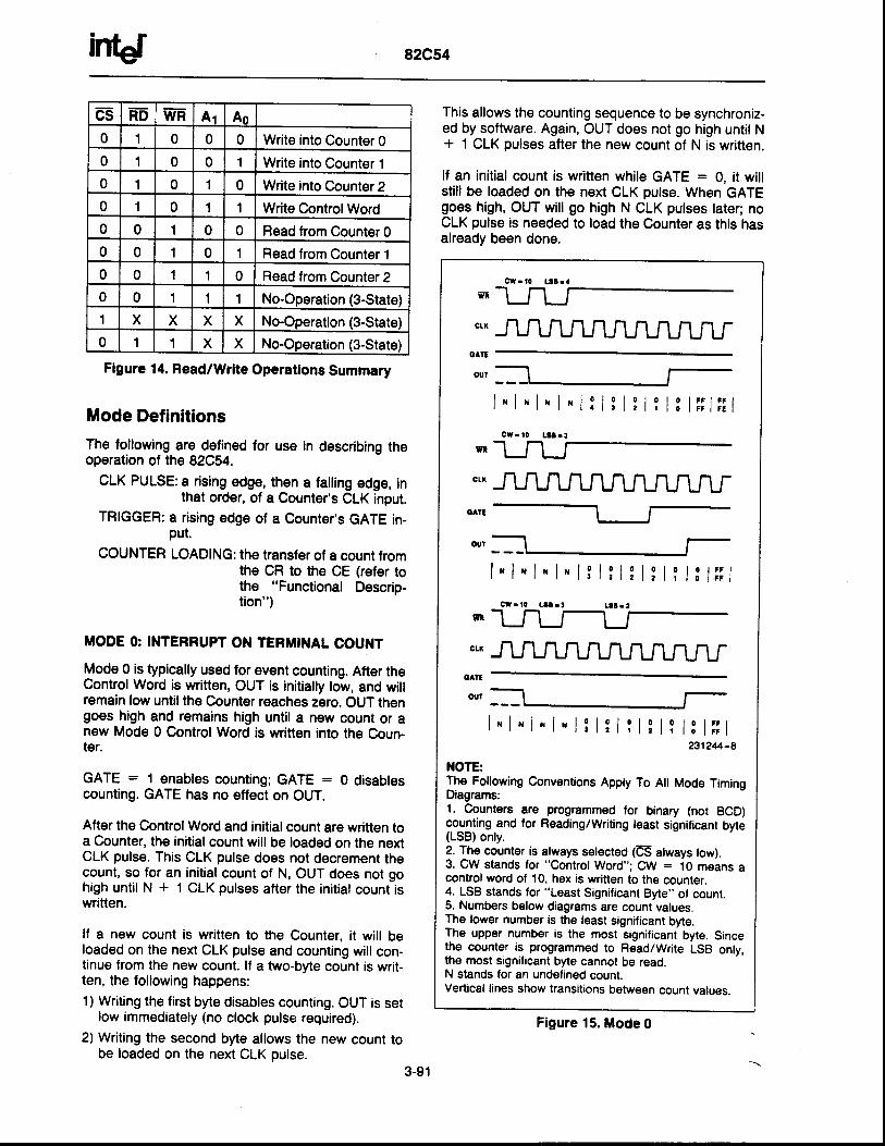
inbr 82C54
es FD WR Ar Ao
0 1 0 0 0 Write into Counter 00 1 0 0 1 Write into Counter 10 I 0 1 0 Write into Counter 20 1 0 1 1 Write ControlWord0 0 1 0 0 Read from Counter 00 0 1 0 1 Read from Counter 10 0 1 1 0 Read from Counter 20 0 1 1 1 No-Operation (3-State)
1 X X X X No-Operation (3-State)
0 1 1 X X No-Operation (3-State)
Flgure 14. Read/Wrlte Operations Summary
Mode DefinitionsThe following are defined for use in describing theoperation of the 82C54.
CLK PULSE: a rising edge, then a falling edge, inthat order, of a Counter,s CLK input.
TRIGGER: a rising edge of a Counter's GATE in-put.
COUNTER LOADING:the transfer of a count fromthe CR to the CE (refer tothe "Functional Descrip-tion")
MODE 0: INTERRUPT ON TERMTNAL COUNT
Mode 0 is typically used for event counting. After theControl Word is written, OUT is initially low, and willremain low untilthe Counter reaches zero. OUT thengoes high and remains high until a new count or anew Mode 0 Control Word is written into the Goun-ter.
GATE : 1 enables counting; GATE : O disablescounting. GATE has no etfect on OUT.
After the Gontrol Word and initial count are written toa Counter, the initial count will be loaded on the nextCLK pulse. This CLK pulse does not decrement thecount, so for an initial count of N, OUT does not gohigh until N + 1 CLK pulses atter the initiat count iswriften.
lf a new count is writlen to the Counter, it will beloaded on the next GLK pulse and counting will con-tinue from the new count. lf a two-byte count is writ-ten, the lollowing happens:1) Writing the first byte disables counting. OUT is set
low immediately (no clock pulse required).2) Writing the second byte allows the new count to
be loaded on the next CLK pulse.3-91
This allows the counting sequence to be synchroniz-ed by sottware. Again, OUT does not go high until N+ 1 CLK pulses after the new count of N is written.
lf an initial count is written while GATE : 0, it willstill be loaded on the next CLK pulse. When GATEgoes high, OUT will go high N CLK pulses later; noCLK pulse is needed to load the Counter as this hasalready been done.
| - l * l * l ' I I I 3 I I I i I s lF| : : lCw- l0 Ll l r t
l " l " l - l " l3 | : I I | : i ? l3 l t : lCwr l0 Lt l r t
l - l " l - l '13l t l t l l l t ls l i i l231244-8
NOTE:The Following Conventions Apply To All Mode TimingDiagrams:1. Counters are programmed for binary (not BCD)gollting and lor Reading/Writing t€ast significant byte(LSB) only.2. The counler is always selected (dS ahays low).3. CW stands for "Control Word"; CW = 10 means acontrol word of 10, hex is written to the counter.4. LSB stands lor "Least Signilicant Byte', of count.5. Numbers below diagrams are count values.The lower number is the least signilicant byte.The upper number is the most significant byte. Sincethe counter is programmed to Read/Write LSB only,the most significant byte cannot be read.N stands lor an undelined count.Vertical lines show transitions between count values.
Figure 15. Mode 0
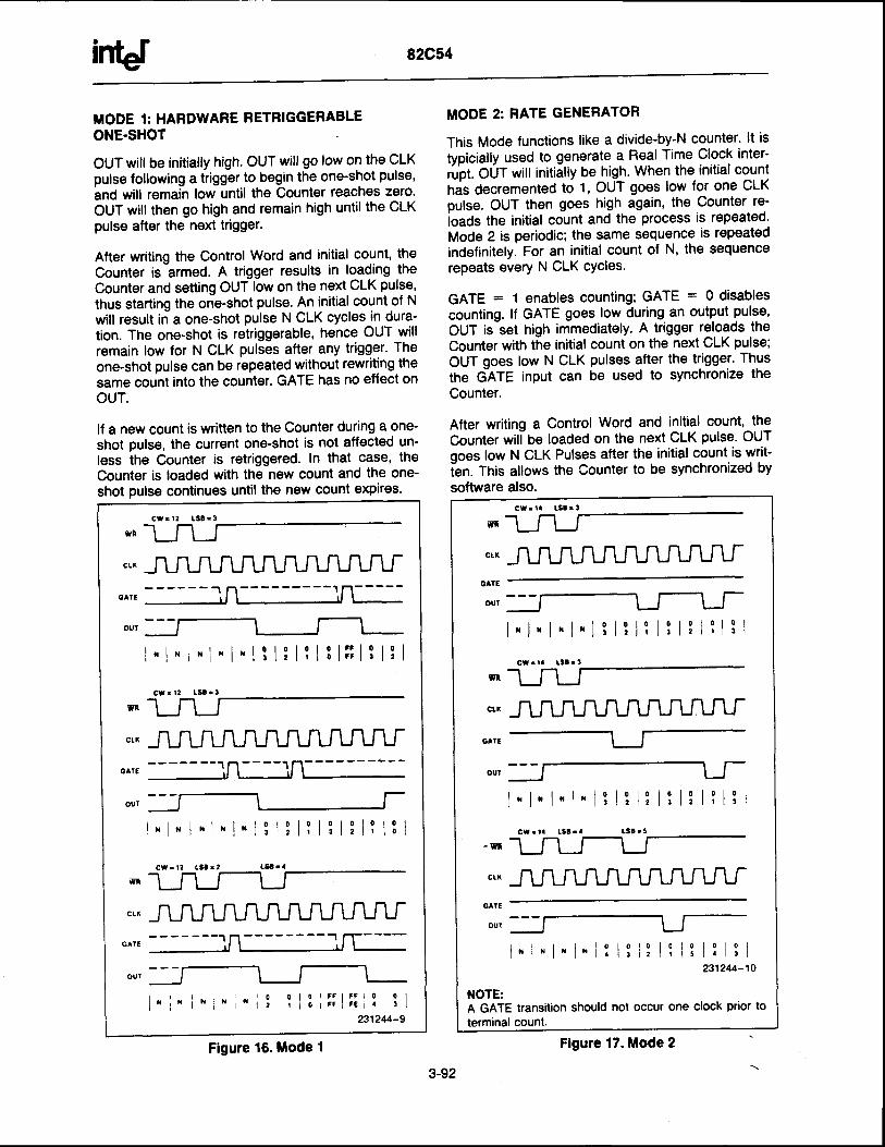
inbf 82C54
iIODE 1: HARDWABE RETRIGGERABLEONE.SHOT
OUT will be initially high. OUT will go low on the CLKpulse following a trigger to begin the one-shot pulse'
and will remain low until the Counter reaches zero'OUT will then go high and remain high until the CLKpulse after the next trigger.
After writing the Control Word and initial count, theCounter is armed. A trigger results in loading theCounter and setting OUT low on the next CLK pulse'thus starting the one-shot pulse. An initial count of Nwill result in a one-shot pulse N CLK cycles in dura-tion. The one-shot is retriggerable, hence OUT willremain low for N CLK pulses after any trigger. Theone-shot pulse can be repeated without rewriting thesame count into the counter' GATE has no effect onOUT.
lf a new count is written to the Counter during a one-shot pulse, the current one-shot is not affected un-less the Counter is retriggered. In that case, theCounter is loaded with the new count and the one-shot pulse continues until the new count expires.
MODE 2: RATE GENERATOR
This Mode functions like a divide-by'N counter' lt is
tvoicially used to generate a Real Time Clock inter',i,pt. OUr will initially be higtr. When the. initial counthas decremented to 1, OUT goes low for one CLKpulse. OUT then goes high again, the Counter re-ioads the initial count and the process is repeated'Mode 2 is periodic; the same sequence is repeatedindefinitely. For an initial count of N, the sequencerepeats every N CLK cYcles.
GATE : 1 enables counting; GATE : 0 disablescounting. It GATE goes low during an output pulse,
OUT is-set high immediately. A trigger reloads theCounter with the initial count on the next CLK pulse;
OUT goes low N CLK pulses after the trigger' Thusthe GATE input can be used to synchronize theCounter.
After writing a Control Word and initial count, theCounter will be loaded on the next CLK pulse. OUTooes low N CLK Pulses after the initial count is writ-ien. This allows the Counter to be synchronized bysoftware also.
FT
ctx
O TE
out
l - l - | r l * | r I I l t l t | 3 l : t l3 | : I
r[
c l x
ol lE
oul
l - l . l x l r l r , l : ! l l l l : l l l i 13 l
CW r t2 Lt! :2 L5! rr
9t
c tx
GAIE
our
l - i - i r r ,x I I i : l l l t : | i l : l : I231244-9
Figure 16. Mode I
wr
cLt
o^rE
oul
wt
cLx
o^rt
our
l ' , l - l - l -13 l : l l l : l l I l l i I
CW. la l8l . a LS! r 3
' 0 [
ctx
ollE
out
l . l . l . l " i : l3 i : l l l : l : l3 I231244-10
NOTE:A GATE transition should not occur one clock prior toterminal count.
3-92
Figure 17. Mode 2
inbr 82C54
Writing a new count while counting does not atfectthe curent counting sequence. lf a trigger is re.ceived after writing a new count but before the endof the current period, the Counter will be loaded withthe new count on the nsxt CLK pulse and countingwill continue from the new count. Othenrvise, th6new count will be loaded at the end of ths currentcounting cycle. ln mode 2, a COUNT of 1 is illegal.
MODE 3: SQUARE WAVE MODE
Jvlole _S is typically used for Baud rate generation.Mode 3 is similar to Mode 2 except for the duty cycleof OUT. OUT witt initiaily be higfr. When hatf ins ini_tial count has expired, OUT goes low for the remain-der of the count. Mode 3 is periodic; the sequenceabove is repeated indefinitely. An initial count of Nresults in a square wave with a period of N CLKcycles.
GATE : 1 enables counting; GATE : 0 disablescounting. lf GATE goes low white OUT is low, OUT isset high immediately; no CLK pulse is required. Atrigger reloads the Counter with the initial count onthe nelrt CLK pulse. Thus the GATE input can beused to synchronize the Counter
After writing a Control Word and initial count, theCounter will be loaded on the next CLK putse. Thisallows the Counter to be synchronized by softwarealso.
Writing a new count while counting does not atfectthe current counting sequence. lf a trigger is re-ceived after writing a new count but before the endof the current hall-cycle of the square wave, theCounter will be loaded with the new count on thenext CLK pulse and counting will continue from thenew count. Othenrise, the new count will be loadedat the end of the current half-cycle.
Mode 3 is implemented as follows:
Even counts: OUT is initiaily high. The initialcount isloaded on one CLK pulse and then is decrementedby two on succeeding CLK pulses. When the countexpires OUT changes value and the Counter is re_loaded with the initiat count. The above process isrepeated indefinitely.
odd counts: oUT is initially high. The initial countminus one (an even number) is loaded on one CLKpulse and then is decremented by two on succeed-ing CLK pulses. One CLK putse after the count ex-pires, OUT goes low and the Counter is reloadedwith the initial count minus one. Succeeding CLKpulses decrement the count by two. When the countexpires, OUT goes high again and the Counter isreloaded with the initial count minus one. The aboveprocess is repeated indefinitely. So for odd counts,
OUT will be high for (N + 1)/2 counts and tow for(N -1)/2 counts.
MODE 4: SOFTWARE TRtccERED STROBE
OUT will be initiaily high. When the initiat counr ex_pires, OUT will go low for one CLK pulse and thengo high again. The counting sequEnce is ,,triggered"by writing the initial count.
GATE : 1 enables counting; GATE : 0 disablescounting. GATE has no effect on OUT.
After writing a Control Word and initial count, theCounter will be loaded on the next CLK pulse. ThisCLK pulse does not decrement the couni, so for aninitial count of N, OUT does not strobe low untilN + 1 CLK pulses after the initial count is written.
lf a new count is written during counting, it will beloaded on the next CLK putse and countiig wiil con_tinue from the new count. lf a two-byte corint is writ-ten, the following happens:
itr
ct t
cAt:
ilr
YT
c!r
oAtt
OI
9t
ctr
oat:
out
NOTE:A GATE transition should not occur one clock prior toterminal count.
l ' l r l i l " l : l t l t l : l t l : l : l s l : l : I
l ' l " l " l . l l l : l t l i l : l | : i | : l 3 l231214-11
Figure 18. Mode 3
3-93

intet 82C54
1) Writing the first byte has no etfect on counting.
2)Writing the second byte allows the new count tobe loaded on the next GLK Pulse.
This allows the sequence to be "retriggered" bysoftware. OUT strobes low N+1 CLK pulses afterthe new count of N is written.
MODE 5: HARDWARE TRIGGERED STROBE(RETBIGGERABLE)
OUT will initially be high. Counting is triggered by arising edge ol GATE. When the initial count has ex-pired, OUT will go low for one CLK pulse and thengo high again.
After writing the Control Word and initial count' thecounter will not be loaded until the CLK pulse afler atrigger. This CLK pulse does not decrement thecount, so for an initial count of N' OUT does notstrobe low until N + 1 CLK pulses after a trigger.
A trigger results in the Counter being loaded with theinitial count on the next CLK pulse. The countingsequence is retriggerable. OUT will not strobe lowfor N * 1 CLK pulses after any trigger' GATE hasno etfect on OUT.
lf a new count is written during counting, the currentcounting seguence will not be affected. lf a triggeroccurs after the new count is written but before thecurrent count expires, the Counter will be loadedwith the new count on the next CLK pulse andcounting will continue from there.
wr
cLx
oiltE
our
l . l - l . l " l : l o l o l o l F F l F F l F r lz l r l o l F F l F E l F o l
w!
c tx
oat:
our
l " l " l ' , l , l3 | 313l : l t lS l f i lCf,. ta Li l .3 Ll t r 2
wt
cLx
o/lt€
out
l " l , . l " l - l : l o l o l o l ol z l r l a l r
l o l F F ll o l r r l231244-12
Figure 19. Mode 4
EI
ctx
gAT:
m
c t r
' :, '.: ':.l,"'
. ',:1.' ' r I : I r I r | 3 r::r
l , l . l r l r l * l l I : l I | : l ; : l : ! l I i : I231244-13
GAIE
ouY
*E
c lx
crlt
out
Flgure 20. Mode 5
3-94

intef 82C54
SlgnalStaturllodcc
LowOr Golng
LowRlrlng Hlgh
0 Disablescounting
Enablescounlinq
1 1) Initiatescounling
2) Resets outputeft€r nextclock
2 1) Disablescounting
2) Sets outputimmediatelyhioh
lnitiatescounting
Enablescounting
3 1) Disablescounting
2) Sets outputimmedialelyhigh
lnitiatescounting
Enablescounting
4 Disablescountino
Enablescountino
5 lnitiatescountino
Flgure 21. Gate Pln Operailom Summary
Operation Common to All Modes
Programmlng
When a Control Word is written to a Counter, allControl Logic is immediately reset and OUT goes toa known initial state; no CLK pulses are required forthis.
GATE
The GATE input is always sampled on the risingedge of CLK. ln Modes 0,2,3, and 4 the GATE inputis level sensitive, and the logic level is sampled onthe rising edge of CLK. ln Modes 1, 2, g, and 5 theGATE inpul is rising-edge sensitive. ln these Modes,a rising edge of GATE (trigger) sets an edge-sensi-tive flip-flop in the Counter. This flip-ftop is then sam-pled on the next rising edge of CLK; the flip-flop isreset immediately after it is sampled. ln this way, atrigger will be detected no matter when it occurs-ahigh logic leveldoes not have to be maintained untilthe next rising edge of CLK. Note that in Modes 2and 3, the GATE input is both edge- and level-sensi-tive. ln Modes 2 and 3, if a GLK source other thanthe system clock is used, GATE should be pulsedimmediately following WF- of a new count value.
COUNTER
New counts are loaded and Counters are decre-mented on the falling edge of CLK.
The largeg! possible initial count is O; this is equiva-lent to 216 tor binary counting and 104 for'BCDcounting.
The Gounter do€s not stop when it reaches zero. lnModes 0, 1, 4, and 5 the Counter "wraps around" tothe highest count, either FFFF hex for binary count-ing or 9999 for BCD counting, and continues count-ing. Modes 2 and 3 are periodic; the Counter reloadsitself with the initial count and continues countingfrom there.
3-95
IIODE MINCOUNT
mAxCOUNT
0 1 01 1 0
2 2 03 2 04 1 0
NOTE:0 is equivalent to 216 lor binary counting and 10a forBCD counting
Figure 22. ilinlmum and ilarlmum InlUalCounts

inbf 82C54
ABSOLUTE MAXIMUM RATINGS*
Ambient Temperature Under Bias.. . . ' ' '0'C to 70"CStorageTemperature . . . . . -65 ' to *150 'CSupp l iVo l tage . . . . . . - 0 .5 to +8 .0VOperat ingVol tage . . . . . +4Vto +7VVoltage on any Input. . . ' GND - 2V to + 6.5VVoltage on any Output . .GND-0.5V to V6s + 0.5VPower Dissipation . . .1 Watt
D.C. CHARACTERISTICSf fR=0'C to 70'C, V66:5Vt 10%, GND:0V) CIn
'Notice: Slresses above those listed under "Abso-lute Maximum Ratings" may cause parmanent dam'age to the device. This is a stress rating only andfunctional operation of the device at these or anyother conditions above those indicated in the opera'tional sections of this specification is not implied' Ex'posure to absotute maximum rating conditions forextanded periods may affect deice reliability.
: -40oC to *85'C for Extended Temperature)
A.C. CHARACTERISTICSfln : 0'C to 7o'C, Vcc : 5V t10o/o, GND :0V) CIn :
BUS PARAMETERS (NOIE 1)
READ CYCLE
-40'C to * 85'C for Extended Temperature)
Symbol Parameter Mln Max Unlts Teet Condltlona
V11 Input Low Voltage -0.5 0.8 V
Vru Input High Voltage 2.0 Vcc + 0.5 V
Vor Outout Low Voltage 0.4 v lnr : 2.5 mA
vox Output High Voltage 3.0Vcc - 0.4
VV
lox : -2.5mAInr.r : -100 rrA
lu lnput Load Cunent x2.0 pA Vrru:Vec to 0V
lopr Output Float Leakage Currenl r 10 pA Vnr m: Vcc to 0.0V
lsc V66 Supply Cunent 20 mA $MHz82C54Cfk Freq: 10MHz g2CS4-2
lccsa V66 Supply Current-StandbY 't0 pA GLK Freq : 96dS: Vcc.All lnputs/Data Bus V66AllOutputs Floatinq
lccser V66 Supply Current-StandbY 150 pA CLK Freq : 96eS : Vcc.AllOther InPuts,l/O Pins = VGND, Outputs Open
Qru Input Capacitance 1 0 PF f s : 1 MHz
Unmeasured pinsreturned to GND(s)
Cvo l/O Capacitance 20 PF
cour Output Capacitance 20 pF
Symbol Parameter82C54 82C54-2 Unlts
Mln Max Mln Mar
tnR Address Stable Before Fi5 J 45 30 ns
tsR 6 staute Betore R-D I 0 0 ns
tRl Address Hold Time Atter FE 1 0 0 ns
tnn m Pulse Width 150 95 ns
tRo Data Elelay trom F-D J 120 85 ns
tno Data Delay from Address 220 185 ns
tor FD 1 to Data Floating a 90 5 65 ns
tRv Command Recovery Time 200 165 ns
NOTE:'1 . AG timings measured at Vq1 : 2.0V' V91 : 0.8V'
3-96

inbf 82C54
A.C. CHARACTERISTICS (continued)
WRITECYCLE
2' ln Modes 1. and 5 triggers are sampled on each rising clock edge. A second trigger within 120 ns (70 ns lor the s2os4-2)of the rising clock edge may not be detected.3. Low-going glitches that violate tpwx, tpult lay cause_ enors requiring counter reprogramming.4. Except lor Extended remp., see Extended remp. A.c. characteristiis below.5. Sampled not 100o/o tested. Trq = 25 C.6' ll CLK Present 9! Twc min then Count equals N+2 CLK pulses, T619 max equals Count N+1 CLK pulse. Twc min toTy76 m€u, count will be either N+ 1 or N+2 CLK pulses.7. In Modes 1 and 5, if GATE is present when writing a new Count value, at Twq min Counter will not be triggered, at Try6max Counter will be triggered.8' lf cLK present when writing a Counter Latch or ReadBack Command, at T6g min CLK will be reflected in count valuelatched' at Tg1 max CLK will not be reflected in the counl value latched. Writirij a Counter t-atctr oi ReaOgacf Com;nJbetween T6g min and Tyyg max will result in a latch€d count vallue which is t one least significant bit.
EXTENDED TEiiIPERATURE O : -40oC to +85'C for Extended T
Symbol Parameter 82C54 82C54-2 UnltsMin ilax Min Max
tew Address Stable Before WFi j 0 0 nstsw 6 Staule Before WFI J 0 0 nstwR Address Hold Time After WFI I 0 0 nstww WR Pulse Width 1 5 0 95 nstow Data Setup Time Before WFI f 120 95 nstwo Data Hold Time AfterWF f 0 0 nstnv Comqand Recovery Time 200 165 ns
CLOCK AND GATE
Symbol Parameter 82C54 82Cs4-2 UnitsMln Max Min Max
tcr-x Clock Period 't25 DC 100 DC nstpwx High Pulse Width 60(3) 30(3) nstpwl Low Pulse Width 60(3) 50(3) nsTs Clock Rise Time 25 25 nstp Clock FallTime 25 25 nstow Gare widrh High 50 50 . nstcl Gate Width Low 50 50 nstes Gate Setup Time to CLK T 50 40 nsteH Gate Hold Time After CLK T 50(2) 50(2) nsToo Output Delay from CLK J 150 100 ns!coo Output Delay from Gate J 120 100 nstwc CLI( Delay for Loading(a) 0 55 0 55 nstwo Gate Delay for Sampling(a) - 5 50 - 5 40 nstwo OUT Delay from Mode Write 260 240 nstcl CLK Set Up for Count Latch -40 45 -40 40 NS
NOTES:
CLK Delay for Loading
3-97
intet 82C54
WAVEFORMS
231244-14
READ
2312U-15
231244-16
3-98

inbf 82C54
CLOCK AND GATE
23121/-17' Lrst byto ot counl belng witen
A.C. TESTING INPUT, OUTPUT WAVEFORIII A.C. TESTING LOAD CIRCUIT
INPUT/OUTPUT
23124-10A.C. Tecring: InputB ar€ drivon at 2.4V tot I togic "1" and 0..f5Vfor a logic "0." Timing mee8ur€mentE aro msd€ !t 2.0V tor s bglc'1" ud 0.8V lor a logic "0."
I orvrcr I| '*17I I ic r . t l r r
I
J
Cl - 150 pFC1 includer fig cepedtanca
23121,4.-19
3-99


APPENDIX D
CONFIGURING THE AD2OOO FOR SIGNAL*MATH

D-2

Jumper Settings
When running SIGNAL*MATH, you have to change some of the AD2000's on-board jumpen from theirfacory-set positions. Before using SIGNAL*MATH on the AD2000 board, check the following jumpers:
.F2- Base address
. P3 - 8254 timer/counter I/O configuration
. P4, P5 &YI - Intemrpts
. P6 - End-of-Convert Monitor
The board layout is shown in Figure D-1.
Fig. D-1 - AD2000 Board Layout
P2 - Base Address
SIGNAL*MATH assumes that the base address of your AD2000 is the factory setting of 300 hex (768 deci-mal). If you change this setting, you must run the ADAINST program and reset the base address.
NOTE: When using the ADAINST program, you can enter the base address in decimal or hexadecimalnotation. When entering a hex value, you must precede the number by a dollar sign (for example, $300).
D-3
IHH_lililqrulmftffiffi_=_LrUli[: U uI f g f t - ? | . - - . l - l
Oreffif"'P8
P3 - t254 Timer/Counter VO Configuration
The 8254 must be configured with the six jumpers placed between the pins as shown in Figure D-2. Aftersetling dre jumpers, verify that each is in the proper location. Any remaining jumpers must be rcmoved from the P3header connector.
XTALECo+5VE@coocoocK1EEE
lsl-q
lsXTALECr+5VEG1co16TcJ<2
XTALrcz+5VECi2cg2co2
lslelrl*l"sls
Fig. D-2 -8254 Timer/Counter Jumpers, P3
P4, PS & P7 - Interrupts
To select IRQ channels and intemrpt sources for SIGNAL*MATH, you must install two jumpers on P5 and onejumper on P7. First install a jumper on P5-OUT2, and a second jumper across the pair of P5 pins for the IRQchannel you select.Then, install a jumper on the end-of+onvert intemrpt header, P7, across the pins of your desiredIRQ channel. The IRQ selected on P7 must be different from the IRQ set on P5! Figure D-3 shows OUT2jumpered to IRQ3 and EOC jumpered to IRQ4. Make sure that no jumpers are installed on P4.
P5 765432olr l O: t5
P7
oo]U
76s-4032
Fig. D-3 - Timer/Counter Out & End-of-Convert lntem;pt Jumpers, P5 & P7
P6 - End-of-Convert Monitor
When running SIGNAL*MATH, place a jumper between EOC and PA7, as shown in Figure D4.
!
Fig. D-4 - End-of-Convert Monitor Jumper, P6
D4
Running ADAINST
After the jumpers are set and the AD2000 board is installed in the computer, you are ready to configureSIGNAL*MATH so that it is compatible with you board's setings. This is done by running the ADAINST driverinstallation program. After running the program, open AD2000.EXE from the Open a File menu. You will see ascreen similar to the screen shown in Figure D-5 below. The factory default serings are shown in the illustration.Your seuings may or may not match the default settings, depending on whether you have made changes to theseseuings before.
Base Address. The board's base address setting is entered in the upper right block, as shown in the diagram.The factory setting for all Real Time Devices boards is 3CI hex (768 decimat). The base address can be entered as adecimal or hexadecimal value (hex values must be preceded by a dollar sign (for example, $3m). Refer to yourboard's manual if you need help in determining the correct value 0o enter.
EOC IT (End-of-Convert Interrupt). In this block, enter the IRQ channel number which corresponds to yourjurnper se$ing on P7.
Timer IT (Timer/Counter Interrupt). In this block, enter the IRQ channel number which corresponds to yourjurnper setting on P5.
LabTech SW IT (LABTECH NOTEBOOK Software Interrupt). This sets the software intemrpt addresswhere LABTECH NOTEBOOK's labLINX driver is installed. The facory sening is $60. This setting can beignored when running SIGNAL*MATH.
A./D Parameters. Six A/D board parameters are listed: resolution, number of channels, active DMA channel,gain, loss, and input voltage polarity.
Endof-ConvertInterrupt Channel
Timer/Counterlnterrupt Ghannel
Fig. D-5 - ADAINST.EXE Screen
Base Address
A/D DMAChannelSelect;
External Gain& Loss
A/D Unipolar/BipolarSelect
SoftwarelnterruptAddress
D/A DMAChannelSelect;
External Gain& Loss
D/A Unipolar/BipolarSelect
D-5

Resolution and number of channels are fixed by the program for your board.
The DMA channel number block is not valid on the AD2000, and should be left blank.
The next two blocks, gain and loss, are provided so that you can make adjustments for external gain or loss,other than the programmable gain settings available on the board. If your input signal is externally attenuated, thenyou can adjust for this by setting a value other than I for loss. Ifyou have an external gain facbr, then you canadjust for this condition. Numbers must be entered as whole decimal values. The factory default sesing for gain andloss is 1.
For a bipolar input range, an X should be placed before Bipolar on the screen (default setting). For unipolarope.ration, remove the X.
D/A Parameters. These six blocks are not used on the AD2000, and should be left blank.
D-6

APPENDIX E
CONFIGURING THE AD2OOO FOR ATLANTIS


Jumper Settings
When running ATLANTIS, you have o change some of the AD2000's on-board jumpers from their facory-setpositions. Before using ATLANTIS on the AD2000 board, check ttre following jumpen:
. F2 - Base address
. P3 - 8254 timer/counter VO configuration
. P4, P5 &Yl - Intemrpts
. P6 - End-of-Convert Monitor
The board layout is shown in Figure E-1.
Fig. E-1 - AD2000 Board Layout
P2 - Base Address
ATLANTIS assumes that the base address of your AD2000 is the factory setting of 300 hex (see Chapter 1). Ifyou changed this setting, you must run tlte ATINST progxam and reset the base address.
NOTE: The ATINST program requires the base address to be entered in decimal notation.
R€l Tima Devi6s, Inq
ffiu*"rnu."n.
ECIi5V
EGIcolcorga
(TA
EC2i6V
EG2
E-3

P3 - 8254 Timer/Counter UO Configuration
T1ne8254 must be configured with the six jumpers placed between the pins as shown in Figure E-2. Aftnrsetting the jumpers, verify that each is in ttre proper location. Any remaining jumpers must be removed from the P3header connector.
Fig. E-2 - 8254 Timer/Counter Jumpers, P3
P4, P5 & P/ - Interrupts
To select an RQ channel and an intemrpt source for ATLANTIS, you must install two jumpers on P5, thetimer/counter output intemrpt header. Jumpers must be installed across the OUT2 pins and across the pins of yourdesired IRQ channel. Figure E-3 shows OUT2 jumpered to IRQ3. lvlake sure ttrat no jumpers are installed across theIRQ pins on header connectors P4 and P7.
Fig. E-3 - End-of Jumper, P7
P6 - End-of-Convert Monitor
When running ATLANTIS, place a jumper between EOC and PA7, as shown in Figure 84.
Fig. E-4 - End-of-Convert Monitor Jumper, P6
XTALECo+5VEC{c@coocK1
XTALECl+5VEG1co16Tcte.
EE
l*1.9
lslsI-eIrl*lsls
[]il-l ;Ll ilc-Convert Inlerrupt
!
E4

APPENDIX F
WARRANTY

F-2

LIMITED WARRANTY
Real Time Devices, Inc. warrants the hardware and software products it manufactures and produces to be freefrom defecs in materials and workmanship for one year following the date of shipment from REAL TIME DE-VICES. This warranty is limited to the original purchaser of product and is not transferable.
During the one year warranty period, REAL TIME DEVICES will repair or replace, at its option, any defectiveproduc8 orparts at no additional charge, provided that the product is returned, shipping prepaid, to REAL TIMEDEVICES. All replaced parts and products become ttre property of REAL TIME DEVICES. Before returning anyproduct for repair, customers are required to contact the factory for an RMA number.
THIS LIMITED WARRANTY DOES NOT EXTEND TO A}.IY PRODUCTS WHICH HAVE BEEN DAM-AGED AS A RESULT OF ACCIDENT, MSUSE, ABUSE (such as: use of incorrect input voltages, improper orinsufficient ventilation, failure to follow the operating instructions that are provided by REAL TIME DEVICES,"acts of God" or other contingencies beyond the control of REAL TIME DEVICES), OR AS A RESULT OFSERVICE OR MODIFICATION BY AI.IYONE OTIIER THAN REAL TIME DEVICES. EXCEPT AS EX-PRESSLY SET FORTH ABOVE, NO OTHER WARRANTIES ARE E)GRESSED OR IMPLIED, INCLUDING,BUT NOT LIMI'IED TO, AI.IY IMPLIED WARRANTIES OF MERCHANTABILITY AND FITNESS FOR APARTICULAR PURPOSE, AND REAL TIME DEVICES E)PRESSLY DISCLAIMS ALL WARRANTIES NOTSTATED HEREIN. ALL IMPLIED WARRANTIES,INCLUDING IMPLTED WARRANTIES FORMECHANTABILITY AND FITNESS FOR A PARTICULAR PURPOSE, ARE LIMITED TO TTIE DURATIONOF THIS WARRANTY. IN TIIE EVENT THE PRODUCT IS NOT FREE FROM DEFECTS AS WARRAN]EDABOVE, TI{E PURCHASER'S SOLE REMEDY SHALL BE REPAIR OR REPLACEMENT AS PROVIDEDABOVE. UNDER NO CIRCUMSTANCES WILL REAL TIME DEVICES BE LIABLE TO TTIE PTIRCHASEROR AI.IY USER FOR AI.IY DAMAGES,INCLUDING AIIY INCIDENTAL OR CONSEQUENTIAL DAM-AGES, E)GENSES, LOST PROFITS, LOST SAVINGS, OR OTI{ER DAMAGES ARISING OUT OF TIIE USEOR INABILITYTOUSE TIIE PRODUCT.
SOME STATES DO NOT ALLOW TI{E EXCLUSION OR LIMITATION OF INCIDENTAL OR CONSE-QUENTIAL DAMAGES FOR CONSUMER PRODUCTS, AND SOME STATES DO NOT ALLOW LIMITA-TIONS ON HOW LONG AN IMPLIED WARRANTY LASTS, SO T}M ABOVE LIMITATIONS OR EXCLU-SIONS MAY NOT APPLY TO YOU.
THIS WARRANTY GIVES YOU SPECIFIC LEGAL RIG}ITS, AND YOU MAY ALSO HAVE OTHERRIGIITS WHICH VARY FROM STATE TO STATE.
F-3

AD2000 User-Selected Options
Base I/O Address:
(hex) (decimal)
IRQ Channel Selection:
A/DEOC IRQ CHANNEL:
PITOUTO IRQ CHANNEL:
PITOUTI IRQ CHANNEL:
PITOUT2 IRQCI{ANNEL:
PPr rNTRA (PC3) IRQ CHANNEL:
EXTINT IRQ CHANNEL:
A/D EOC/PPI Bit Assignment:
A/D EOC PA?:
PC7: