Embed Size (px)
Citation preview

École Polytechnique Fédérale de Lausanne
Politecnico di Torino
Institut National Polytechnique de Grenoble
____________________
Master’s degree in Micro and Nano Technologies
for Integrated Systems
Master’s Thesis
A/D Converter based on Binary Search
Algorithm
Candidate Supervisors
Fedele FERRARA Prof. Alexandre SCHMID
Prof. Fabrizio PIRRI
Nikola KATIC
Lausanne, August 2012

A/D Converter based on Binary Search Algorithm ____________________________________________________________________________________________________________
_______________________________________________________________________________ Page 2 Microelectronic Systems Laboratory, EPFL F. Ferrara

A/D Converter based on Binary Search Algorithm ____________________________________________________________________________________________________________
_______________________________________________________________________________ F. Ferrara Microelectronic Systems Laboratory, EPFL Page 3
Table of Contents
List of Figures and Tables .................................................................................................... 5
List of Acronyms .................................................................................................................. 7
Abstract ................................................................................................................................ 9
Thesis Contents Organization ............................................................................................ 10
Chapter 1 - Introduction ............................................................................................. 11
Chapter 2 - ADC Architecture & Design ...................................................................... 13
2.1 Binary Search Algorithm ........................................................................................... 13
2.2 ADC based on SC Techniques with Op-Amp ............................................................ 15
2.3 ADC based on SC Techniques with ZCD ................................................................... 16
2.4 Custom Modifications of the Original Design ......................................................... 17
2.5 Limitations and Advantages of the ZCD Implementation ....................................... 18
2.6 ADC Performances Evaluation ................................................................................. 18
2.6.1 Static Simulations .............................................................................................. 18
2.6.2 Dynamic Simulations ......................................................................................... 19
Chapter 3 – Building Blocks Design ............................................................................. 21
3.1 Bootstrapped Switch ................................................................................................ 21
3.1.1 Introduction ....................................................................................................... 21
3.1.2 Primary Configuration ....................................................................................... 22
3.1.3 Alternative Configuration ................................................................................. 24
3.1.4 Limitations and Improvements ........................................................................ 25
3.1.5 Simulations and Results .................................................................................... 29
3.2 Zero-Crossing Detector ............................................................................................ 33
3.2.1 Introduction ....................................................................................................... 33
3.2.2 Zero-Crossing Detection: Principle of Operation .............................................. 33
3.2.3 Transistor Level Implementation ..................................................................... 37

A/D Converter based on Binary Search Algorithm ____________________________________________________________________________________________________________
_______________________________________________________________________________ Page 4 Microelectronic Systems Laboratory, EPFL F. Ferrara
3.2.4 Alternative ZCD Implementation ...................................................................... 40
3.2.5 Simulations ....................................................................................................... 42
3.3 Comparator .............................................................................................................. 45
3.4 SAR Logic .................................................................................................................. 46
3.5 Current Sources ........................................................................................................ 48
3.6 Voltage Reference .................................................................................................... 49
Chapter 4 – Simulations & Results............................................................................... 51
4.1 Functional Simulations ............................................................................................. 51
4.2 Performance Simulations ........................................................................................ 53
Chapter 5 – Conclusions & Future Perspective ............................................................ 57
Acknowledgement ............................................................................................................. 59
References ......................................................................................................................... 61
Appendix ............................................................................................................................ 63
Appendix A ............................................................................................................. 63
Appendix B ............................................................................................................. 65

A/D Converter based on Binary Search Algorithm ____________________________________________________________________________________________________________
_______________________________________________________________________________ F. Ferrara Microelectronic Systems Laboratory, EPFL Page 5
List of Figures and Tables
Fig. 2.1 SAR ADC Block Diagram ........................................................................................ .13
Fig. 2.2 Block Diagram based on Binary Search Algorithm .............................................. .14
Fig. 2.3 ADC architecture with Op-Amp ........................................................................... .15
Fig. 2.4 Control Circuit for and ......................................................................... .16
Fig. 2.5 ADC Architecture with ZCD Implementation ...................................................... .17
Fig. 2.6 Detail of the Implementation for the additional switches .................................. .17
Fig. 3.1 Bootstrap basic circuit .......................................................................................... .21
Fig. 3.2 Transistor level Implementation ......................................................................... .22
Fig. 3.3 Input and Output voltage waveforms of the bootstrap switch .......................... .23
Fig. 3.4 Gate Voltage Variation vs. Time .......................................................................... .24
Fig. 3.5 Transistor level Implementation ......................................................................... .25
Fig. 3.6 Charge Injection Mechanism ................................................................................ .26
Fig. 3.7 Clock Feedthrough Mechanism ............................................................................ .27
Fig. 3.8 Dummy Switch CF Implementation ..................................................................... .28
Fig. 3.9 Bootstrap Switch Schematic with Dummy Transistors ....................................... .29
Fig. 3.10 Testbench configuration .................................................................................... .30
Fig. 3.11 Input and Output Voltage for Testbench Simulation ........................................ .31
Fig. 3.12 Spectrum of the first bootstrap switch configuration ....................................... .32
Fig. 3.13 Spectrum of the second bootstrap switch configuration ................................. .32
Fig. 3.14 Timing Diagram .................................................................................................. .33
Fig. 3.15 Preset Phase (P) .................................................................................................. .34
Fig. 3.16 Coarse Charge Transfer Phase (E1) .................................................................... .35
Fig. 3.17 Fine Charge Transfer Phase (E2)......................................................................... .36
Fig. 3.18 Zero-Crossing Detector Implementation .......................................................... .37

A/D Converter based on Binary Search Algorithm ____________________________________________________________________________________________________________
_______________________________________________________________________________ Page 6 Microelectronic Systems Laboratory, EPFL F. Ferrara
Fig. 3.19 Time Diagram of the ZCD .................................................................................. .38
Fig. 3.20 Control signal Implementation .......................................................................... .39
Fig. 3.21 Edge Detector Falling ......................................................................................... .39
Fig. 3.22 Alternative Zero-Crossing Detector Implementation ........................................ .40
Fig. 3.23 Time diagram for the second ZCD Implementation .......................................... .41
Fig. 3.24 Edge Detector Rising ......................................................................................... .42
Fig. 3.25 Stimuli for Offset Simulation of a Comparator .................................................. .43
Fig. 3.26 Cumulative Histogram and Normal Probability Plot for single ended ZCD ....... .44
Fig. 3.27 Cumulative Histogram and Normal Probability Plot for fully differential ZCD . .44
Fig. 3.28 Schematic of the Dynamic Latch ....................................................................... .45
Fig. 3.29 Schematic of the comparator ............................................................................ .46
Fig. 3.30 Schematic of the SAR Logic ............................................................................... .47
Fig. 3.31 Current sources ................................................................................................. .48
Fig. 3.32 Voltage reference circuit ................................................................................... .49
Fig. 3.33 Time diagram for the reference circuit ............................................................. .50
Fig. 4.1 Input and Output voltage of ZCBC ....................................................................... .51
Fig. 4.2 Input and Output voltage of ZCD ........................................................................ .52
Fig. 4.3 Input and Output of ZCBC with voltage reference circuit ................................... .52
Fig. 4.4 Detail of Comparison ............................................................................................ .53
Fig. 4.5 INL Plot ................................................................................................................. .54
Fig. 4.6 DNL Plot ................................................................................................................ .55
Fig. 4.7 Spectrum of Quantized Output ............................................................................ .55
Fig. 4.8 ADC Transfer Curve .............................................................................................. .56
Table 3.1 Bootstrapped Switches Simulation Results ...................................................... .30
Table 3.2 Simulations Results for ZCD implementations ................................................. .43
Table 4.2 ADC Performance Summary ............................................................................. .54

A/D Converter based on Binary Search Algorithm ____________________________________________________________________________________________________________
_______________________________________________________________________________ F. Ferrara Microelectronic Systems Laboratory, EPFL Page 7
List of acronyms
ADC - Analog to Digital Converter
SC - Switched Capacitor
ZCBC - Zero-Crossing Based Circuit
Op-Amp - Operational Amplifier
SAR - Successive Approximation Register
S&H - Sample & Hold
BSA - Binary Search Algorithm
DAC - Digital to Analog Converter
ZCD - Zero-Crossing Detector
SNR - Signal to Noise Ratio
SNDR - Signal to Noise and Distortion Ratio
ENOB - Effective Number of Bits
FFT - Fast Fourier Transform
FOM - Figure of Merit
FF - Flip-Flop
DTDL - Dynamic Threshold Detecting Latch
INL - Integral Non Linearity
DNL - Differential Non Linearity
MSB - Most Significant Bit
LSB - Least Significant Bit

A/D Converter based on Binary Search Algorithm ____________________________________________________________________________________________________________
_______________________________________________________________________________ Page 8 Microelectronic Systems Laboratory, EPFL F. Ferrara

A/D Converter based on Binary Search Algorithm ____________________________________________________________________________________________________________
_______________________________________________________________________________ F. Ferrara Microelectronic Systems Laboratory, EPFL Page 9
Abstract
Nowadays, CMOS technology scaling introduces many new challenges in analog mixed-
signal circuit design, as a large variety of potential applications requires a very power
efficient system implementation. In most cases, Analog to Digital Converters (ADCs) are
the most relevant power consumers in these systems, therefore, the minimization of
their power consumption is a crucial design issue for the fulfillment of the specifications
imposed by the market.
In order to meet the low power consumption requirements, a Switched Capacitor (SC)
ADC, based on the Binary Search Algorithm, is presented in this report. A SC circuit
consists of switches, capacitors and a gain stage, obtained by means of the capacitors
ratio. A crucial element of traditional SC circuits is the Operation Amplifier (Op-Amp),
but, in CMOS implementation, especially when moving to deep submicron technologies,
Op-Amps pose difficult challenges for their design. Due to this, a zero-crossing based
circuit (ZCBC) has been introduced in this project. The ZCBC relies on the novel concept
of zero-crossing detection, which simplifies the design of SC circuits. Moreover, it results
in better performance, especially in the power reduction, making it more suitable for
scaled CMOS technologies.
In this master thesis project, a 10 bits Binary Search ADC has been implemented, using
standard UMC 180 nm CMOS technology with a power supply of 1.8V. The ADC operates
at a sampling frequency of 166 kHz and achieves nearly 8.7 effective bits. Fully
differential configuration is implemented to achieve higher ADC performance.
Bootstrapped switches are used to perform the sampling operation with the distortion
level. The complete ADC draws no static current and consumes less than 58 of
power.

A/D Converter based on Binary Search Algorithm ____________________________________________________________________________________________________________
_______________________________________________________________________________ Page 10 Microelectronic Systems Laboratory, EPFL F. Ferrara
Thesis Contents Organization
Chapter 1 provides an overall introduction to the work presented in this report,
explaining motivations and constraints of the design, together with some possible
applications.
In Chapter 2 the Binary Search Algorithm is explained in detail. Subsequently, two
possible architectures, both based on SC implementation, are described. The first
configuration is implemented with a traditional Op-Amp, while the second one replaces
the Op-Amp by using the novel concept of Zero-Crossing Detection. Limitations and
advantages of each configuration are described, together with the challenging issues of
the design.
In Chapter 3 the basic analog building blocks of the ADC architecture are presented. The
described blocks are the bootstrapped switches, the ZCD block, the comparator, the
current sources, the SAR logic and the voltage reference circuit. Furthermore,
alternative implementations with respect to the initial ones are proposed for some of
the circuits. Simulation details are also provided, with the particular emphasis on the
ZCD offset estimation and on Signal to Noise Ratio (SNR) and Signal to Noise and
Distortion Ratio (SNDR) measurements for the bootstrapped switches.
Chapter 4 is completely dedicated to simulations, including functionality and overall
performance of the design architecture. In particular, Integral Non Linearity (INL) and
Differential Non Linearity (DNL) are computed, as well as the SNR and SNDR of the ADC.
Finally, in Chapter 5, the conclusions of the project are presented, including future
perspective and improvements.

A/D Converter based on Binary Search Algorithm ____________________________________________________________________________________________________________
_______________________________________________________________________________ F. Ferrara Microelectronic Systems Laboratory, EPFL Page 11
Chapter 1
Introduction
In the recent years an increasing interest has been focused on the design of biomedical
wireless sensors [1], since they can be used for online monitoring, detection and
prevention of many diseases, reducing drastically hospital costs [2].
Most biomedical signals are characterized by low frequency range (tens of kHz) [3] and
by low voltage amplitude. Moreover, they usually contain a high DC offset, due to the
electrode, that needs to be suppressed. A typical biomedical sensor consists of a band-
pass filter, a low-noise programmable amplifier and an Analog to Digital Converter
(ADC), [2].
The most important constraint in the design of biomedical sensors is the power
reduction, due to the fact that they are isolated from any external power supply source.
As a consequence, the design of ADCs has been focused on low power demanding
architecture.
The ADC architecture proposed in this master thesis is a Binary Search ADC, based on
the Switched Capacitor (SC) implementation, which solves many of the limitations of
classical Successive Approximation Register (SAR) implementation. Indeed, in CMOS
technology SC circuits have often been chosen because their gain depends only on the
ratio between the capacitances, rather than on the value of a single capacitor. This
allows bypassing the problem related to the difficulty in obtaining accurate capacitance
values in integrated CMOS processes.
An element of critical importance in the design of traditional SC circuits is the
Operational Amplifier (Op-Amp). Due to the technology scaling, the Op-Amp design
faces difficult design challenges [4]. In fact, lower voltage supply and lower output
resistance, in scaled CMOS technologies, result in low dynamic range and lower intrinsic
device gain, which lead to difficulties in the realization of accurate charge transfers [5].
A possible solution to keep the same dynamic range is to increase the circuit
capacitances, but this solution will increase the total power consumption. Moreover,
cascoded amplifier stages have been used to increase intrinsic gain but they further
reduce the signal swing, which is already low in deep submicron CMOS technology since
the voltage supply is scaled too.

A/D Converter based on Binary Search Algorithm ____________________________________________________________________________________________________________
_______________________________________________________________________________ Page 12 Microelectronic Systems Laboratory, EPFL F. Ferrara
Another approach to deal with technology and voltage scaling is an alternative
architecture called Zero-Crossing Based Circuits (ZCBC) [4]. This implementation uses a
combination of a comparator and current sources to perform the same charge transfer
as Op-Amp based circuitry, reducing both design complexity and power consumption.

A/D Converter based on Binary Search Algorithm ____________________________________________________________________________________________________________
_______________________________________________________________________________ F. Ferrara Microelectronic Systems Laboratory, EPFL Page 13
Chapter 2
ADC Architecture & Design
2.1 Binary Search Algorithm
The Binary Search Algorithm represents the basis of the Successive Approximation
Conversion principle, which performs the analog-to-digital conversion by using the
previously determined bits to set the decision condition for the next significant bit.
Thanks to this method, it is possible to reduce the power consumption and to increase
the conversion efficiency of the circuit.
In Fig. 2.1, the block diagram for an n-bit SA ADC is shown. The ADC is typically
consisted of four subcircuits: a sample and hold circuit (S&H) to acquire the input
voltage, a voltage comparator which compares the sampled input and the output of the
internal DAC, a Successive Approximation Register (SAR) designed to convert the analog
output of the comparator to the digital code and, finally, the internal DAC, placed in the
feedback loop, used to supply the reference comparison level to the comparator. The
analog reference comparison value corresponds to the digital code of the SAR logic.
Fig. 2.1 SAR ADC Block Diagram
Among all the available ADC architectures, the SAR ADC circuit has been often
considered as the most efficient configuration to digitalize biomedical signals.

A/D Converter based on Binary Search Algorithm ____________________________________________________________________________________________________________
_______________________________________________________________________________ Page 14 Microelectronic Systems Laboratory, EPFL F. Ferrara
Nevertheless, the SAR ADC architectures, especially those based on capacitive DAC,
present some disadvantages which hinder their design [2]:
- Large area occupation, for the capacitive DAC, especially in the case of Binary
Weighted Arrays (BWA), which requires a large die area for implementation.
- Large switching power consumption, in fact, although the overall power
consumption is kept low, large peaks of currents from the supply voltage can be
observed. These peaks can seriously jeopardize the performance of the
converter.
- Parasitic capacitances, which can reduce the accuracy of the capacitive DAC and
also affect the design performance.
As a result of all these mentioned drawbacks, an alternative architecture, based on
Binary Search Algorithm, is presented, [2]. This configuration eliminates the need for
DAC circuit, as shown in the block diagram (Fig. 2.2) and it is implemented using
Switched-Capacitor (SC) Circuits.
Fig. 2.2 Block Diagram based on Binary Search Algorithm
The principle of operation of this architecture is quite straightforward. Indeed, it begins
when the sampled input is compared with a certain threshold voltage to set the
Most Significant Bit (MSB). Subsequently, depending on the result of the first
comparison, a reference voltage will be added or subtracted and a new
comparison will be performed to set the second bit. After that, ,divided by two, will
be added or subtracted again. In order to complete the conversion, the cycle needs to
be repeated as many times as the number of bits of the A/D converter.
In the following sections, two ADC architectures based on the binary search algorithm
are presented. Both configurations are implemented by using a Switched-Capacitor
A/D Converter based on Binary Search Algorithm ____________________________________________________________________________________________________________
_______________________________________________________________________________ F. Ferrara Microelectronic Systems Laboratory, EPFL Page 15
technique. However, while in the first architecture a traditional operational amplifier is
used, in the second one the Op-Amp is replaced by a comparator, based on the Zero
Crossing Detection principle, which will be explained in detail later on in this report, in
section 3.2.
The fully-differential mode was chosen due to its numerous advantages with respect to
the single ended one. In fact, in addition to simplifying the sum and subtraction
operations with the reference voltage, it allows to increase the input swing and it
reduces charge injections errors, since only the difference between the two inputs
signals is considered.
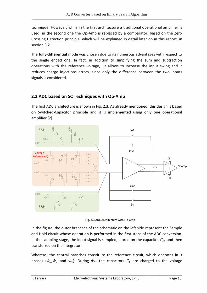
2.2 ADC based on SC Techniques with Op-Amp
The first ADC architecture is shown in Fig. 2.3. As already mentioned, this design is based
on Switched-Capacitor principle and it is implemented using only one operational
amplifier [2].
In the figure, the outer branches of the schematic on the left side represent the Sample
and Hold circuit whose operation is performed in the first steps of the ADC conversion.
In the sampling stage, the input signal is sampled, stored on the capacitor and then
transferred on the integrator.
Whereas, the central branches constitute the reference circuit, which operates in 3
phases ( and ). During , the capacitors are charged to the voltage
Fig. 2.3 ADC Architecture with Op-Amp
A/D Converter based on Binary Search Algorithm ____________________________________________________________________________________________________________
_______________________________________________________________________________ Page 16 Microelectronic Systems Laboratory, EPFL F. Ferrara
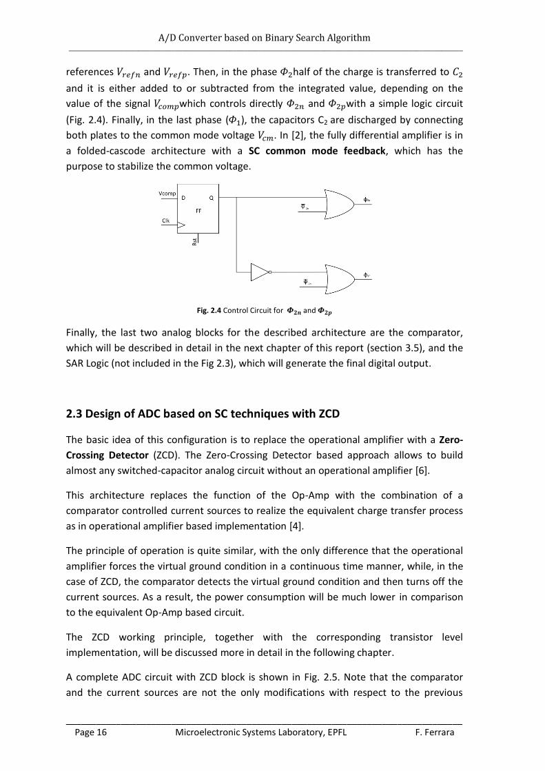
references and . Then, in the phase half of the charge is transferred to
and it is either added to or subtracted from the integrated value, depending on the
value of the signal which controls directly and with a simple logic circuit
(Fig. 2.4). Finally, in the last phase ( ), the capacitors C2 are discharged by connecting
both plates to the common mode voltage . In [2], the fully differential amplifier is in
a folded-cascode architecture with a SC common mode feedback, which has the
purpose to stabilize the common voltage.
Fig. 2.4 Control Circuit for and
Finally, the last two analog blocks for the described architecture are the comparator,
which will be described in detail in the next chapter of this report (section 3.5), and the
SAR Logic (not included in the Fig 2.3), which will generate the final digital output.
2.3 Design of ADC based on SC techniques with ZCD
The basic idea of this configuration is to replace the operational amplifier with a Zero-
Crossing Detector (ZCD). The Zero-Crossing Detector based approach allows to build
almost any switched-capacitor analog circuit without an operational amplifier [6].
This architecture replaces the function of the Op-Amp with the combination of a
comparator controlled current sources to realize the equivalent charge transfer process
as in operational amplifier based implementation [4].
The principle of operation is quite similar, with the only difference that the operational
amplifier forces the virtual ground condition in a continuous time manner, while, in the
case of ZCD, the comparator detects the virtual ground condition and then turns off the
current sources. As a result, the power consumption will be much lower in comparison
to the equivalent Op-Amp based circuit.
The ZCD working principle, together with the corresponding transistor level
implementation, will be discussed more in detail in the following chapter.
A complete ADC circuit with ZCD block is shown in Fig. 2.5. Note that the comparator
and the current sources are not the only modifications with respect to the previous

A/D Converter based on Binary Search Algorithm ____________________________________________________________________________________________________________
_______________________________________________________________________________ F. Ferrara Microelectronic Systems Laboratory, EPFL Page 17
configuration. In fact, the reference voltage is modified and additional switches are
added between the load capacitances, as explained in the section 2.4.
Fig. 2.5 ADC Architecture with ZCD Implementation
2.4 Custom Modifications of the Original Design
As mentioned previously, the ZCD is not the only change
introduced in the design: the main additional modification consists
of the voltage reference circuit. In this second version, operates in
3 phases instead of two. Indeed, since the comparator is no more
forcing the virtual ground condition in a continuous way as in the
Op-Amp based circuit, an extra-phase is needed to ensure that the
half of the charge from C1 is effectively transferred to C2.
Furthermore, three additional switches are needed between the
two load capacitances [4], as shown in detail in Fig. 2.6. Note that
the switches M2+ and M2- are open after the reset phase, while
M1 is kept closed to connect the load capacitors until the ZCD
detects the virtual ground condition. Hence, M1 ties together the
Fig. 2.6 Implementation of the Additional
Switches

A/D Converter based on Binary Search Algorithm ____________________________________________________________________________________________________________
_______________________________________________________________________________ Page 18 Microelectronic Systems Laboratory, EPFL F. Ferrara
inside plates of the capacitors, but allows the voltage on that node to float while outputs
are ramping. As a result, both capacitors will charge at the same rate regardless of any
current mismatch in current sources and thus no common mode charge error will be
accumulated.
The last difference is that in this last configuration there is no common mode feedback
circuit [4]. This is why the output voltage common mode is set by the current sources
which charge the capacitors and does not depend on the performance of the ZCD. Any
mismatch between current sources is absorbed by the load capacitors and produces a
small voltage common mode error, but, since this error gets reset every cycle in ZCD, the
SC common mode feedback circuit is not needed in this architecture.
2.5 Limitations and Advantages of ZCD Implementation
A possible limitation for ZCDs is coming from the offset compensation, which, due to
technology scaling, is becoming increasingly important for analog circuit design. In fact,
the traditional closed-loop offset cancelation techniques are not applicable to Zero
Crossing Based Circuits (ZCBC). The offset that affects a ZCBC is a dynamic one and
cannot be corrected via closed-loop techniques, used for static offset compensation.
However, in order to overcome this limitation, derivative techniques have been
developed [4].
On the other hand, the main advantage of the ZCD implementation is the power
efficiency in comparison to the traditional operational amplifier, because the
comparator is turning off as soon as the virtual ground condition is detected. In addition
to this, ZCBCs are more amenable for scaled CMOS technology, because the design of a
ZCD does not require any high-gain or high-speed feedback loop to stabilize the circuit,
that on the contrary pose difficult challenges for the design of Op-Amps in deep sub-
micron technologies [4]. As a result, the implementation with zero-crossing reduces the
complexity of the design.
Considering all the above, in the next chapter of the report, all the analog building blocks
for the second ADC architecture will be discussed in detail, including transistor level
implementation and behavioral simulations.
2.6 ADC Performances Evaluation
2.6.1 Static Simulations
The static performances of ADCs are evaluated by the nonlinearity, which can be
characterized in different ways: differential or integral [16]. The Differential

A/D Converter based on Binary Search Algorithm ____________________________________________________________________________________________________________
_______________________________________________________________________________ F. Ferrara Microelectronic Systems Laboratory, EPFL Page 19
Nonlinearity (DNL) describes the maximum difference between the theoretical and the
real transfer function of an ADC, measured between adjacent Least Significant Bit (LSB)
values over the full conversion range.
For a particular digital output signal of the ADC, the DNL values are:
(2.1)
The Integral Nonlinearity (INL) indicates the maximum deviation of transfer function
from its ideal transfer function, with gain and offset errors set to be zero.
The relationship between the DNL and the INL is described by the following equation
(2.2):
(2.2)
2.6.2 Dynamic Simulations
The Signal to Noise Ratio (SNR) is one of the most important parameters to evaluate the
dynamic performances of ADCs, since it describes the resolution of the converter in
dynamic range. It compares the peak-to-peak full scale input signal to the level of
background noise, which, neglecting external noise sources, is given by the quantization
error ε.
According to [16], if the input signal is a sine wave, the theoretical value of SNR in dBs
can be expressed as:
(2.3)
Where N denotes the number of bits of the ADC. Moreover, considering that, usually the
SNR value is computed with the spectrum analyzer, the Effective number of Bits (ENOB)
can be deduced from the previous formula (2.3):
(2.4)
The parameter ENOB represents a comprehensive evaluation of ADCs, because it covers
all possible errors of A/D conversion, including missing code, clock jitter and other types
of noise.

A/D Converter based on Binary Search Algorithm ____________________________________________________________________________________________________________
_______________________________________________________________________________ Page 20 Microelectronic Systems Laboratory, EPFL F. Ferrara
Even if, in the literature, usually, the definition of ENOB is not based on SNR, but rather
on Signal to Noise and Distortion Ratio (SNDR), as follows:
(2.5)
The SNDR is defined as the ratio of the root-mean-square (RMS) value of the input signal
to root mean value of root-sum-square (RSS) of all other spectral components, except
from DC ones, [17]. Basically, the difference with the SNR is that the SNDR includes
spectral components of all harmonics, while in SNR the first 5 harmonics are not taken
into account. Thus, the measured values of SNR are higher than measured values of
SNDR.

A/D Converter based on Binary Search Algorithm ____________________________________________________________________________________________________________
_______________________________________________________________________________ F. Ferrara Microelectronic Systems Laboratory, EPFL Page 21
Chapter 3
Building blocks design
3.1 Bootstrapped Switch
3.1.1 Introduction
In switched capacitor (SC) circuits, the switches have to provide fast and accurate
charging of sampling capacitor, avoiding a degradation of the signal. The main reason for
degradation is the dependence of the switch resistance on the input voltage.
For this reason, the usage of a simple MOSFET as a switch, results in signal distortion. In
fact, the On-Resistance of a simple MOS switch with source and drain connected as
switch terminals and the control signal on its gate, depends on the gate-source voltage
drop according to the following formula (3.1):
(3.1)
Where and are respectively the gate-source voltage and the threshold voltage,
while can be expressed as a function of the MOS dimensions ( and ) and of the
oxide thickness , as follows:
(3.2)
Additional problems for a single MOS input switch could come from the scaling down of
the CMOS technology. Indeed, reducing the power supply, switch resistance
dramatically increases and a reliable linear conduction is more difficult to obtain. In
addition to this, threshold voltage does not scale at the same ratio as for the supply
voltage, so, in these conditions, the MOS switch is not conducting in a large portion of
the input voltage range.
The bootstrapping technique[7] allows the input signal to swing from rail to rail and it is
fully compatible with low voltage operation, requiring minimal extra hardware.
Bootstrapped switch guarantees maximum conductance, independently of the input,
providing a constant gate-source voltage of the switching transistor during the ON state.

A/D Converter based on Binary Search Algorithm ____________________________________________________________________________________________________________
_______________________________________________________________________________ Page 22 Microelectronic Systems Laboratory, EPFL F. Ferrara
Fig. 3.1 Bootstrap basic circuit
The schematic (in Fig. 3.1) shows the switching transistor MNSW, together with five
additional switches and an additional capacitor . During phase, the capacitor is
charged to through switches S3 and S4, while S5 ties the gate voltage of
MNSW to to ensure that the transistor is switched off. During phase , switches S1
and S2 are closed, putting the charged capacitor in series with the input voltage. Hence,
the gate-source voltage of MNSW is kept constant and equal to the across the capacitor
(approximately ).
3.1.2 Primary Configuration
Transistor level schematic of the bootstrapped switch is shown in Fig. 3.2. The switching
operation is controlled with a single phase clock . In the figure, the ideal switches
(from S1 to S5) are replaced respectively with transistors MN1, MP2, MN3, MP4 and
MN5, [8]. Furthermore, additional transistors are added in order to extend the
functionality and to limit the gate-source voltage, so that the relative terminal voltage
can maximally reach for all the devices.
Fig. 3.2 Transistor level Implementation

A/D Converter based on Binary Search Algorithm ____________________________________________________________________________________________________________
_______________________________________________________________________________ F. Ferrara Microelectronic Systems Laboratory, EPFL Page 23
For instance, the transistors MN7 and MP6 ensure that the gate-source voltage of MP2
does not exceed during phase and during . The problem with this
configuration is that, in order to make MN7 conducting, MP2 should be already
conducting, thus a further transistor (MN8) is needed as a startup to force MP2
conducting. Moreover, the transistor MN9 was added in series to MN5 to limit its gate-
drain voltage and avoid reaching , during . In addition to that, it should be
observed that the bulk of PMOSs must be connected to the highest potential and so for
example to node B and not to .
Finally, note that the value for the capacitor must be sufficiently large to supply
enough charge to the gate of the main switch MNSW, while it is in the ON state.
Otherwise the boosted voltage will be reduced by parasitic capacitances, according to
the formula:
(3.3)
Where is the total parasitic capacitance connected to the top plate of during the
ON state. Therefore, in order to avoid a significant reduction of the boosted voltage, a
value of 500fF was chosen, to be able to consider the effect of negligible.
The output of this bootstrap switch, in a simple sample and hold configuration, is shown
in the following figure (Fig. 3.3), where the sampling frequency is set to 1MHz and the
input is a sine wave with a peak-to-peak amplitude of 1.8V.
Fig. 3.3 Input and Output voltage waveforms of the bootstrap switch

A/D Converter based on Binary Search Algorithm ____________________________________________________________________________________________________________
_______________________________________________________________________________ Page 24 Microelectronic Systems Laboratory, EPFL F. Ferrara
Moreover, Fig. 3.4 shows the voltage variation on the gate of MNSW . Indeed, when
the switch is ON, is greater than the input voltage by a fixed difference of . This
confirms the proper operation, since the gate-source voltage of MNSW is constant and
independent of the input signal.
Fig. 3.4 Gate Voltage Variation vs. Time
3.1.3 Alternative Configuration
In addition to the already mentioned configuration, another possible design for the
bootstrap switch is presented [9]. This version (Fig. 3.5) is quite similar to the previous
one, with the only difference that the PMOS transistor MP4 is replaced by an NMOS
(MN4). Transistor MN4 is controlled by a clock multiplier, formed by transistors MN10
and MN11 together with two capacitors (C1 and C2).
The aim of this circuit is to increase the overdrive voltage ( ) on transistor MN4
in order to ensure the linear region operation and, consequently, a low on-resistance.
The clock multiplier is basically a high voltage generator circuit [10]. In fact, by applying a
square wave input signal of , both C1 and C2 are charged to through the cross
coupled NMOS transistors. As a result, an inverted square wave of almost is
generated at the output of the clock multiplier.
Note that the output voltage value is not exactly doubled because we need to take into
account the parasitic capacitances present in the circuit.

A/D Converter based on Binary Search Algorithm ____________________________________________________________________________________________________________
_______________________________________________________________________________ F. Ferrara Microelectronic Systems Laboratory, EPFL Page 25
Fig. 3.5 Transistor level Implementation
3.1.4 Limitations and Improvements
The major limitation of the bootstrapped switch performance comes from the
disturbance of the sampled input sampled voltage when the MOS switch is turned off.
The main causes for this loss in accuracy are charge injection, clock feedthrough and
thermal noise.
The thermal noise is an electronic noise due to the thermal agitation of the charge
carriers, regardless of any applied voltage and, when is referred to a capacitor, is also
known as KTC noise. In order to determine the minimum value for the load capacitance,
the following relation can be used (3.4):
Then, considering that is equal to the maximum input swing divided by , so
and that (or 1258 in linear value) for a 10 bits
ADC, the following relation (3.5) is obtained:
(3.4)
(3.5)

A/D Converter based on Binary Search Algorithm ____________________________________________________________________________________________________________
_______________________________________________________________________________ Page 26 Microelectronic Systems Laboratory, EPFL F. Ferrara
Thus, according to (3.5), it is possible to determine that the minimum value for the load
capacitance is 16fF. Assuming that the chosen value for will be much higher, due
to capacitor matching, it can be observed that the effect of thermal noise is negligible in
this circuit.
Among all the previous mentioned issues, charge injection is the most important. It
could be explained using the following figure (Fig. 3.6), [11].
Fig. 3.6 Charge Injection Mechanism
When the MOS transistor is on and is small, the charge under the gate oxide
resulting from the inverted channel is
(3.6)
Then, when the MOS turns off, this charge will be injected both into the load
capacitance and into voltage supply. Since the input can be considered as a low
impedance node, this injection has no effect on it. Instead, the injected charge will
change the voltage across the load capacitance .
If the control signal turns off fast, the channel charge distributes approximately equally
between the input and the load capacitance. Thus the change in voltage across
is:
(3.7)
which means that the total voltage across is:
(3.8)

A/D Converter based on Binary Search Algorithm ____________________________________________________________________________________________________________
_______________________________________________________________________________ F. Ferrara Microelectronic Systems Laboratory, EPFL Page 27
From (3.8), it can be noticed that the voltage across is nonlinear with respect to
the due to threshold voltage. Therefore, charge injection results in nonlinearity
errors.
The second problem refers to clock feedthrough [11] (shown in Fig. 3.7), which can be
defined as the coupling between the control signal on the transistor gate of the switch
and the analog signal passing through the transistor. In fact, when the signal is high, it
feeds through the gate-drain and gate-source overlap capacitances (in red in Fig. 3.7),
but since the transistor is turning on, is charged to Vin and the clock feedthrough
has no real effect on the final value of the output. Instead, when goes low and the
MOS transistor turns off, a capacitive divider is created between the gate-source (or
gate drain) capacitance and .
Fig. 3.7 Clock Feedthrough Mechanism
As a result, an offset voltage will be generated across the load, according to the
following formula:
(3.9)
Where is the overlap capacitance that can be expressed as
, with representing the length of the source/drain overlap.
The simplest method to reduce the effects of clock feedthrough and charge injection on
the bootstrap switches is to increase the value of the load capacitance. However, this is

A/D Converter based on Binary Search Algorithm ____________________________________________________________________________________________________________
_______________________________________________________________________________ Page 28 Microelectronic Systems Laboratory, EPFL F. Ferrara
not an efficient solution since it would require a large IC area and it would significantly
increase the power consumption.
Many clock-feedthrough cancelation methods have been presented in literature. One of
the most widely used is dummy switch, as shown in Fig. 3.8.
Fig. 3.8 Dummy Switch CF Cancelation
A dummy switch, M2 in this case, is a normal MOS transistor, with its source and its
drain short-circuited, placed in series with the desired switch M1. The clock signal
controlling its gate is an inverted version of the original clock When M1 turns off a
part of the channel charge is injected toward the dummy transistor, in which regardless
of the shorting, a channel is still created by applying a voltage on its gate. The charge
injected by M1 is compensated by the charge induced by M2 and the global charge
injection cancels out.
If the control clock signal frequency is high enough, there will be approximately equal
splitting of the charge between the source and the drain of the MOS transistor.
Therefore M2 should match with half of the charge injected by M1. As a result, the
width of the dummy transistors is half of that of the MOS transistor, while keeping the
same length L.
In the case of the two previously presented configurations for the bootstrap switches,
two dummy transistors were placed: the former at the output node (D1) and the latter
at the gate of MP2 (D2) [12], as shown in Fig. 3.9.

A/D Converter based on Binary Search Algorithm ____________________________________________________________________________________________________________
_______________________________________________________________________________ F. Ferrara Microelectronic Systems Laboratory, EPFL Page 29
Fig. 3.9 Bootstrap Switch Schematic with Dummy Transistors.
Note that the two dummy transistors (in red) were placed exactly at the same position
also for the second switch configuration.
Finally, another method for canceling charge injection and clock feedthrough is to use a
fully-differential circuit topology. Since in this case we are considering the difference
between the positive and the negative output, the voltage offsets induced on both sides
will cancel out, resulting in the better switching performance.
3.1.5 Simulations and Results
As already explained in a previous chapter of this report, SNR and SNDR are the most
important parameters to evaluate the dynamic performances of an A/D converter. In
this work, they were used also to estimate the performance of the two bootstrapped
switches. The results were obtained using spectral simulations and the spectrum of
sampled outputs were computed using MATLAB® and Fast Fourier Transform (FFT).
In order to guarantee that the signal power (for a single input frequency) is contained
within a FFT bin, a coherent sampling was used, according to the following equation
(3.10):

A/D Converter based on Binary Search Algorithm ____________________________________________________________________________________________________________
_______________________________________________________________________________ Page 30 Microelectronic Systems Laboratory, EPFL F. Ferrara
(3.10)
Where and represent the input and sampling frequency, while and are
respectively the number of cycles and the number of samples for the FFT and they are
relatively prime numbers. Moreover, with the aim of avoid undersampling, the ratio
should be smaller than 0.5.
In the following simulations, in order to fulfil these criteria, M and were set
respectively to and 101. Considering that the sampling frequency was
equal to 1MHz, the frequency of the input sine is set to 98632.8125Hz, according to the
formula.
Fig. 3.10 Testbench configuration
Fig. 3.10 shows the schematic for testbench. Note that a fully differential configuration
was chosen in order to minimize the impact of charge injection and clock feedthrough
on both SNR and SNDR measurements. Furthermore, two capacitors per side were used,
instead of simple track-and-hold circuit, so as to test the switches in a configuration
more similar to that of the final ADC circuit. The capacitor values are set to 500fF.
The input and output voltage waveforms are shown in Fig. 3.11.

A/D Converter based on Binary Search Algorithm ____________________________________________________________________________________________________________
_______________________________________________________________________________ F. Ferrara Microelectronic Systems Laboratory, EPFL Page 31
Fig. 3.11 Input and Output Voltage for Testbench Simulation
SNR and SDNR values were computed for both bootstrapped switches and presented in the following table (Table 3.1), together with sampled outputs spectra for both cases (in Fig. 3.12 and 3.13):
Table 3.1 Bootstrapped Switches Simulation Results
Note that the second configuration indicates the one with the clock multiplier circuit.
Switch Configuration
SNR (dB) SNDR(dB)
First 87,5 77,0
Second 87,4 82,1

A/D Converter based on Binary Search Algorithm ____________________________________________________________________________________________________________
_______________________________________________________________________________ Page 32 Microelectronic Systems Laboratory, EPFL F. Ferrara
Fig. 3.12 Spectrum of the first bootstrap switch configuration
Fig. 3.13 Spectrum of the second bootstrap switch configuration
From the data analysis, especially considering SNDR values, which take into account
distortion, it clearly appears that the both switches have largely satisfying performances
for usage in a 10 bits A/D converter. It may be noticed that the performance of second
bootstrap switch is slightly higher than for the first one.
Considering that the performance of the first switch is already satisfying and that in the
second implementation we would need four MOS transistors and two capacitors more,
the first configuration is chosen to be implemented in the final ADC circuit.
A/D Converter based on Binary Search Algorithm ____________________________________________________________________________________________________________
_______________________________________________________________________________ F. Ferrara Microelectronic Systems Laboratory, EPFL Page 33
3.2 Zero-Crossing Detector
3.2.1 Introduction
As already mentioned in the previous chapter of the report, the ZCBCs have been
introduced as alternative configurations to traditional operational amplifier based
switched capacitor circuits. The ZCBCs are replacing the functionality of the Op-Amp,
using only a comparator (ZCD) and comparator controlled current sources. The main
difference between Op-Amp and ZCD is that the latter is only detecting the virtual
ground condition instead of forcing it continuously in time, so as to reduce considerably
power consumption, since the comparator can be switched off after the condition is
detected. In the following section the ZCD implementation is presented in detail,
including transistor level design and simulations.
3.2.2 Zero-Crossing Detection: Principle of Operation
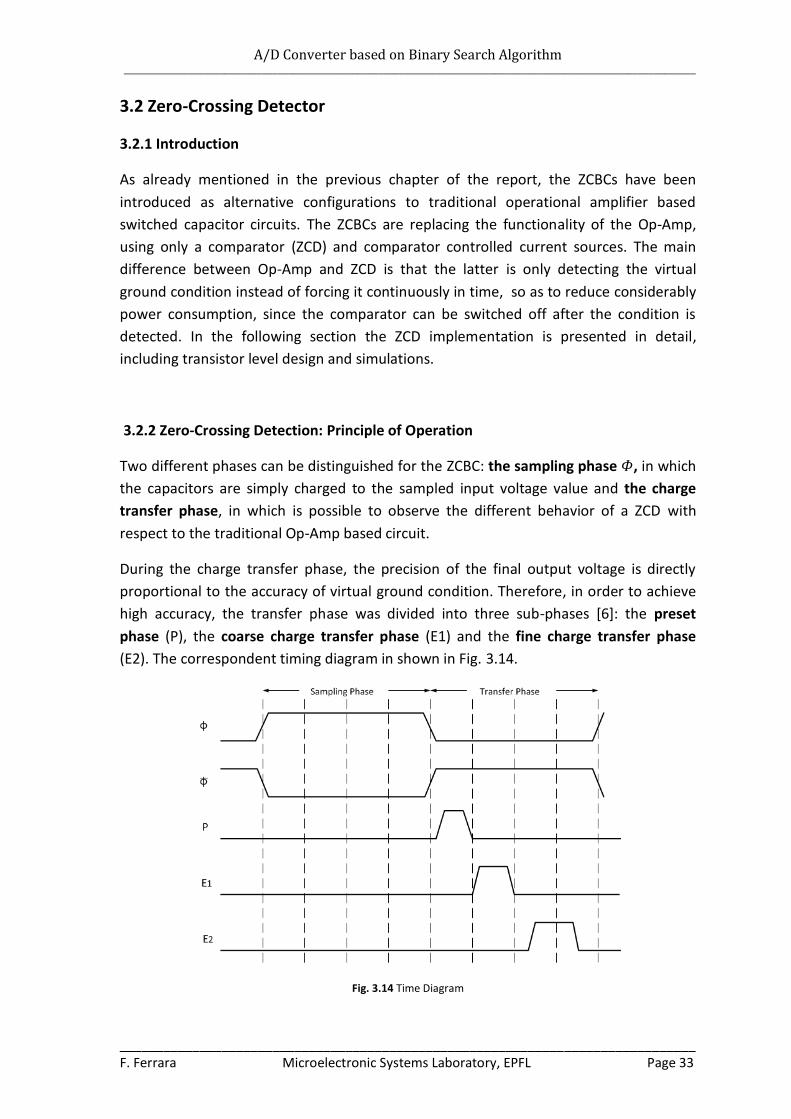
Two different phases can be distinguished for the ZCBC: the sampling phase , in which
the capacitors are simply charged to the sampled input voltage value and the charge
transfer phase, in which is possible to observe the different behavior of a ZCD with
respect to the traditional Op-Amp based circuit.
During the charge transfer phase, the precision of the final output voltage is directly
proportional to the accuracy of virtual ground condition. Therefore, in order to achieve
high accuracy, the transfer phase was divided into three sub-phases [6]: the preset
phase (P), the coarse charge transfer phase (E1) and the fine charge transfer phase
(E2). The correspondent timing diagram in shown in Fig. 3.14.
Fig. 3.14 Time Diagram

A/D Converter based on Binary Search Algorithm ____________________________________________________________________________________________________________
_______________________________________________________________________________ Page 34 Microelectronic Systems Laboratory, EPFL F. Ferrara
In order to achieve higher accuracy, it would be possible to divide the charge transfer in
more than three sub-phases, but in this way further limitations for the sampling
frequency and power consumption would be introduced. Moreover, since three sub-
phases are already enough to obtain precise charge transfer, this possibility was rejected
so as to have a more balanced trade-off between accuracy and speed of the circuit.
The behavior of the ZCD, during the preset phase is shown in Fig. 3.15. This brief phase is
used to ensure that the voltages and start from the condition:
(3.11)
Fig. 3.15 Preset Phase (P)
In fact, after the sampling phase, both and are equal to subsequently, during
the preset phase (P), the output nodes and are connected respectively to lowest
and highest system voltages. Thus, the preset values for the summing nodes and
are:
(3.12)
(3.13)

A/D Converter based on Binary Search Algorithm ____________________________________________________________________________________________________________
_______________________________________________________________________________ F. Ferrara Microelectronic Systems Laboratory, EPFL Page 35
Considering that , the two equations can be simplified as follows:
(3.14)
(3.15)
Thus, using the condition (3.11), it can be stated that the voltage range required for
differential input, in order to keep the output between supply power rails, is from 0 to
.
The second phase of the charge transfer corresponds to the coarse transfer phase (E1),
shown in Fig. 3.15, in which a fast and rough estimation of the virtual ground condition
takes place. This phase begins when the two current sources turn on to charge up the
capacitive network. As a consequence, the ramp voltages are generated for the
summing nodes ( and ) and the output ones ( and ).
As shown in Fig. 3.16, the voltages continue to ramp up (or down) until the virtual
ground condition is detected ( ). Then, the current sources are switched off by
the comparator through the control signal E1. The delay between reaching the virtual
ground condition and turning off of the current sources, results in a finite overshoot as
indicated in Fig. 3.16.
Fig. 3.16 Coarse Charge Transfer Phase (E1)

A/D Converter based on Binary Search Algorithm ____________________________________________________________________________________________________________
_______________________________________________________________________________ Page 36 Microelectronic Systems Laboratory, EPFL F. Ferrara
In order to obtain a more accurate value for the output voltage, the fine transfer phase
(E2) (shown in Fig. 3.17) is used to correct the overshoot coming from the coarse
transfer phase. In this case, the current sources are activated as soon as the phase E1
finishes and they discharge all the capacitive network, creating ramp waveforms with
the opposite slope with respect to E1. The voltages keep ramping until the virtual
ground condition is met again, turning off both the current sources.
Note that the current sources used for E2 conduct less current in comparison with the
ones used in the previous phase, so the delay of the comparator in this case will cause
an error called undershoot, much smaller than the overshoot at the end of the coarse
transfer phase.
Fig. 3.17 Fine Charge Transfer Phase (E2)
Observe that the time spent in E1 or E2 is not fixed, but is signal dependent. To obtain a
correct charge transfer phase, it has to be guaranteed that for any voltage value of the
differential input there will be enough time to complete properly the whole charge
transfer phase. Furthermore, it can be noticed that for systems with high accuracy and
moderate speed as in this case, the above described charge transfer provides the best
compromise, in terms of Figure of Merit (FOM), especially if the time spent on fine
charge transfer phase (E2) is long in comparison with the time spent during the coarse
transfer phase (E1).
A/D Converter based on Binary Search Algorithm ____________________________________________________________________________________________________________
_______________________________________________________________________________ F. Ferrara Microelectronic Systems Laboratory, EPFL Page 37
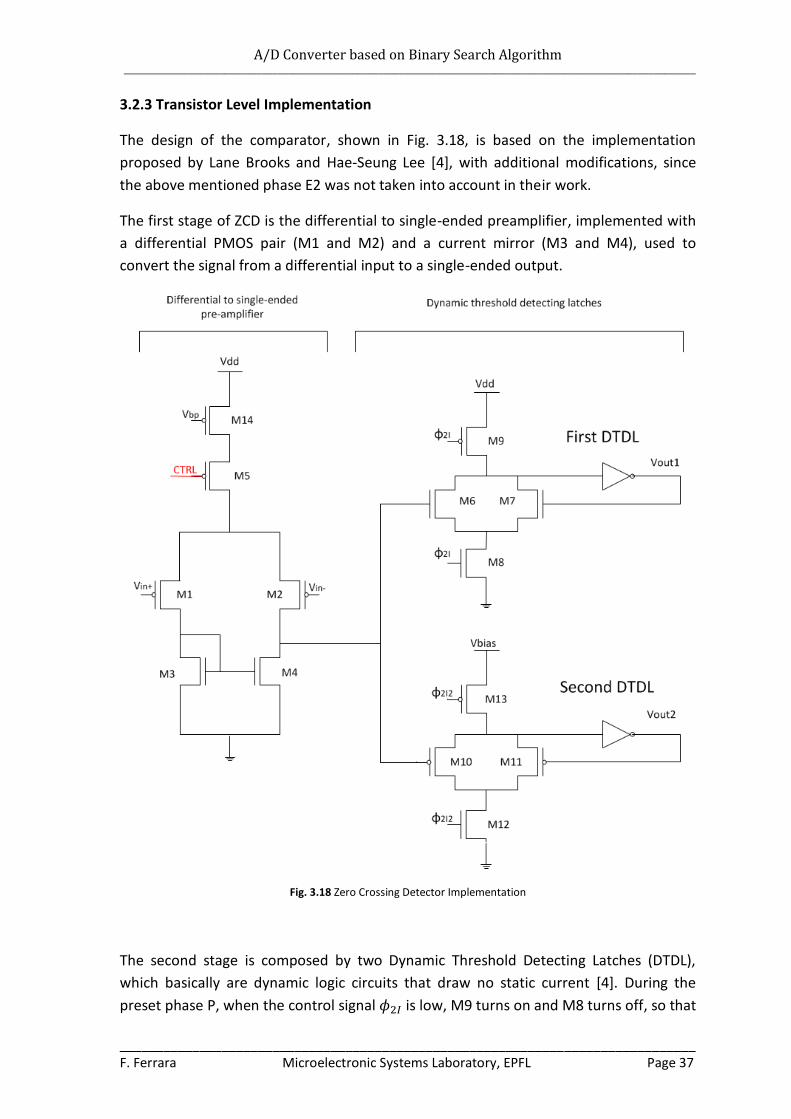
3.2.3 Transistor Level Implementation
The design of the comparator, shown in Fig. 3.18, is based on the implementation
proposed by Lane Brooks and Hae-Seung Lee [4], with additional modifications, since
the above mentioned phase E2 was not taken into account in their work.
The first stage of ZCD is the differential to single-ended preamplifier, implemented with
a differential PMOS pair (M1 and M2) and a current mirror (M3 and M4), used to
convert the signal from a differential input to a single-ended output.
Fig. 3.18 Zero Crossing Detector Implementation
The second stage is composed by two Dynamic Threshold Detecting Latches (DTDL),
which basically are dynamic logic circuits that draw no static current [4]. During the
preset phase P, when the control signal is low, M9 turns on and M8 turns off, so that

A/D Converter based on Binary Search Algorithm ____________________________________________________________________________________________________________
_______________________________________________________________________________ Page 38 Microelectronic Systems Laboratory, EPFL F. Ferrara
the latch is reset. At this point, the bias current of the pre-amplifier stage is turned on
via switch M5. When goes high, in order to enter the charge transfer phase, the
voltage begins to raise. Once the virtual ground has been reached ( ), the
first zero-crossing is detected and raises sufficiently to flip the state of the latch.
As already mentioned in the previous section, the finite delay of the comparator causes
an error in the detection of the virtual ground condition (overshoot). In this
implementation the overshoot is corrected using the second DTDL, which allows to
obtain a more accurate detection of the virtual ground condition.
The rising edge of creates a positive pulse on the signal , which turns on M12
and turns off M13, resetting the second latch. After that, the virtual ground condition is
detected for a second time and drops enough to flip the state of the second DTDL. At
this point, the bias current of the pre-amplifier is shut off by disabling the transistor M5.
The detailed timing diagram is shown in Fig 3.19.
Fig. 3.19 Time Diagram of the ZCD
A/D Converter based on Binary Search Algorithm ____________________________________________________________________________________________________________
_______________________________________________________________________________ F. Ferrara Microelectronic Systems Laboratory, EPFL Page 39
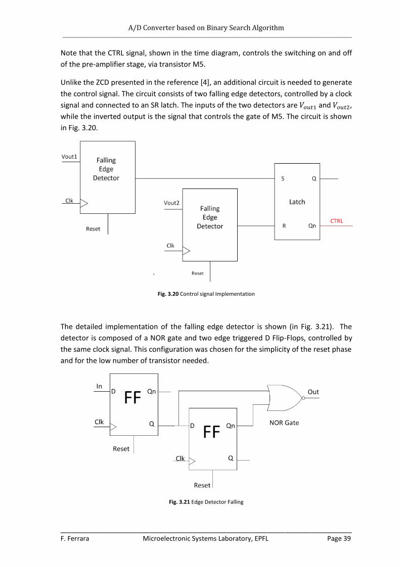
Note that the CTRL signal, shown in the time diagram, controls the switching on and off
of the pre-amplifier stage, via transistor M5.
Unlike the ZCD presented in the reference [4], an additional circuit is needed to generate
the control signal. The circuit consists of two falling edge detectors, controlled by a clock
signal and connected to an SR latch. The inputs of the two detectors are and ,
while the inverted output is the signal that controls the gate of M5. The circuit is shown
in Fig. 3.20.
Fig. 3.20 Control signal Implementation
The detailed implementation of the falling edge detector is shown (in Fig. 3.21). The
detector is composed of a NOR gate and two edge triggered D Flip-Flops, controlled by
the same clock signal. This configuration was chosen for the simplicity of the reset phase
and for the low number of transistor needed.
Fig. 3.21 Edge Detector Falling

A/D Converter based on Binary Search Algorithm ____________________________________________________________________________________________________________
_______________________________________________________________________________ Page 40 Microelectronic Systems Laboratory, EPFL F. Ferrara
3.2.4 Alternative ZCD Implementation
In addition to the previously described ZCD configuration, another implementation is
presented (Fig. 3.22), with the purpose of reducing the systematic static offset of the
comparator. In order to do so, the previous pre-amplifier with single-ended output is
replaced by a differential input to differential output configuration. This pre-amplifier is
implemented as a PMOS differential (M1 and M2) pair which imbalances a pair of cross-
coupled current mirrors (M3, M18, M17 and M4), creating the differential output.
Fig. 3.22 Alternative Zero Cross Detector Implementation

A/D Converter based on Binary Search Algorithm ____________________________________________________________________________________________________________
_______________________________________________________________________________ F. Ferrara Microelectronic Systems Laboratory, EPFL Page 41
Regarding the second stage, the working principle for the first DTDL is the same as
described previously, since the voltage V1 remains unchanged. Whereas, the principle of
operation of the second DTDL changes, because the signal used is no more the voltage
(but rather ).
In this implementation, the rising edge of the ZCD output causes a negative pulse
on that resets the second latch. When goes high again, the voltage begins to
raise, until the virtual ground condition is achieved for the second time and has raised
enough to flip the state of the DTDL.
Note that the implementation of the second DTDL is slightly different from the first one,
in fact, a current mirror (M15 and M16) was placed in the second latch in order to add a
further voltage drop between the source of M10 and the drain of M12. As a result, the
gate voltage required on the gate of M10, to make it conduct, increases. This
modification was needed, due to the nature of the signal , for the shift in the DC
operating point.
The time diagram for the new implementation is shown in Fig. 3.23.
Fig. 3.23 Time diagram for the second ZCD Implementation
A/D Converter based on Binary Search Algorithm ____________________________________________________________________________________________________________
_______________________________________________________________________________ Page 42 Microelectronic Systems Laboratory, EPFL F. Ferrara
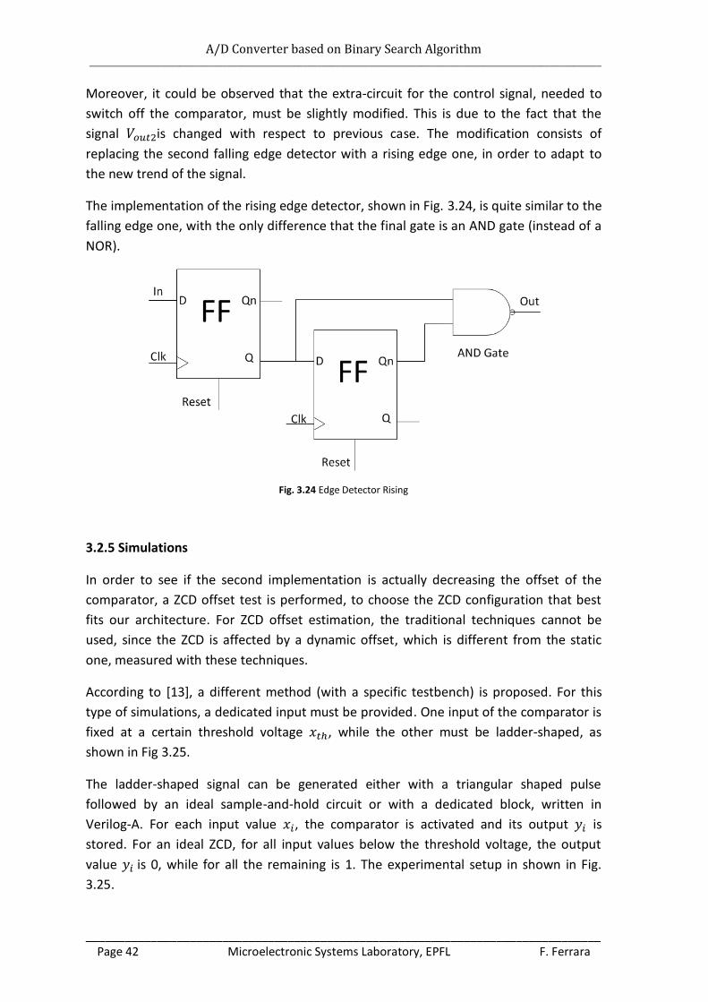
Moreover, it could be observed that the extra-circuit for the control signal, needed to
switch off the comparator, must be slightly modified. This is due to the fact that the
signal is changed with respect to previous case. The modification consists of
replacing the second falling edge detector with a rising edge one, in order to adapt to
the new trend of the signal.
The implementation of the rising edge detector, shown in Fig. 3.24, is quite similar to the
falling edge one, with the only difference that the final gate is an AND gate (instead of a
NOR).
Fig. 3.24 Edge Detector Rising
3.2.5 Simulations
In order to see if the second implementation is actually decreasing the offset of the
comparator, a ZCD offset test is performed, to choose the ZCD configuration that best
fits our architecture. For ZCD offset estimation, the traditional techniques cannot be
used, since the ZCD is affected by a dynamic offset, which is different from the static
one, measured with these techniques.
According to [13], a different method (with a specific testbench) is proposed. For this
type of simulations, a dedicated input must be provided. One input of the comparator is
fixed at a certain threshold voltage , while the other must be ladder-shaped, as
shown in Fig 3.25.
The ladder-shaped signal can be generated either with a triangular shaped pulse
followed by an ideal sample-and-hold circuit or with a dedicated block, written in
Verilog-A. For each input value , the comparator is activated and its output is
stored. For an ideal ZCD, for all input values below the threshold voltage, the output
value is 0, while for all the remaining is 1. The experimental setup in shown in Fig.
3.25.

A/D Converter based on Binary Search Algorithm ____________________________________________________________________________________________________________
_______________________________________________________________________________ F. Ferrara Microelectronic Systems Laboratory, EPFL Page 43
Taking into account the device parameter mismatch, this behavior will randomly change.
Fig. 3.25 Stimuli for Offset Simulation of a Comparator
In order to evaluate the influence of random device parameter variation, Monte-Carlo
analysis was performed and the result of each Monte-Carlo simulation was collected.
For each input value, the probability that the output value is 1 is:
(3.16)
Where is the number of Monte-Carlo iterations and is the number of runs in which
the comparator output is 1 when is applied. Thus, the statistical properties of can
be computed, plotting the normal probability distribution [13].
In order to generate a normal probability plot, the inverse of the cumulative normal
distribution function is applied to the :
(3.17)
Where
(3.18)
The results of 100 Monte-Carlo analysis runs are given for both single ended and fully
differential implementation, respectively in Fig. 3.26 and Fig. 3.27.
Ideally, the comparator threshold should be , so in the simulations xi is set in
the interval:

A/D Converter based on Binary Search Algorithm ____________________________________________________________________________________________________________
_______________________________________________________________________________ Page 44 Microelectronic Systems Laboratory, EPFL F. Ferrara
Fig. 3.26 Cumulative Histogram and Normal Probability Plot for single ended ZCD
Fig. 3.27 Cumulative Histogram and Normal Probability Plot for fully differential ZCD
Note that, in both Fig. 3.26 and Fig. 3.27, the blue lines in the normal probability plots
represent the first order polynomial approximation ( ) of the acquired data.
From the polynomial coefficients and , the mean value and the standard
deviation of the distribution can be computed:
(3.19)

A/D Converter based on Binary Search Algorithm ____________________________________________________________________________________________________________
_______________________________________________________________________________ F. Ferrara Microelectronic Systems Laboratory, EPFL Page 45
The data for both configurations are presented in the following table (Table 3.2).
Table 3.2 Simulations Results for ZCD implementations
From the results of the simulations, it can be observed the mean value and the
standard deviation are practically the same in both configurations. From the results,
we can conclude that the two implementations are equivalent.
On the other hand, it can be noticed that, analyzing the cumulative histograms, the
hysteresis curve for the fully differential implementation is less pronounced with respect
to the single one. For this reason, the fully differential configuration was chosen and
implemented in the ZCBC.
3.3 Comparator
The comparator is a key block in ADC architecture, since it defines the accuracy and is
one of the highest power consumers. It must be designed carefully in order to optimize
power consumption, avoiding at the same time a degradation in the performance of the
ADC [2]. Fig. 3.28 shows the schematic of the proposed solution for the comparator
[14], a current-controlled dynamic-latch.
Fig. 3.28 Schematics of the Dynamic Latch
ZCD (mV) (mV)
Single ended 885 3.2
Fully differential 884 3.1

A/D Converter based on Binary Search Algorithm ____________________________________________________________________________________________________________
_______________________________________________________________________________ Page 46 Microelectronic Systems Laboratory, EPFL F. Ferrara
The dynamic latch is formed by a NMOS differential pair (M2 and M3), which is loaded
by positive feedback network based on a pair of cross-coupled inverters. When the
control signal turns on, the differential pair transforms the input voltage into a
current imbalance which is regenerated and latched by the feedback network to obtain
a binary differential output voltage [14].
Then, the outputs of the comparator drive an RS latch, as shown in the Fig. 3.29, which
gives the single ended output of the comparator , that will control the voltage
reference circuit.
Fig. 3.29 Schematic of the comparator
3.4 SAR Logic
The purpose of the Successive Approximation Register (SAR) circuit is to determine the
value of each bit of the ADC in a sequential manner, depending on the value of the
comparator output.
If an N bit A/D converter is implemented, there are possible conversion output
values, which means that the SAR needs at least states and so, as a minimum, N FFs.
The architecture proposed in [15], uses the minimum number of FFs and is based on the
dependency of the state of each bit with the other bits state. The principle of operation
of the SAR logic is very simple: the algorithm of the conversion starts with the activation
of the Most Significant Bit (MSB), while all the other bits are 0. Then, going on with the
conversion, the remaining bits are successively activated, while the value of the one
activated just before is depending on the result of the comparator [2].
The basic structure of the SAR is a multiple input N bit shift register. At the initial step, in
order to start the conversion, all the FFs are forced in the initialization state. Then, for

A/D Converter based on Binary Search Algorithm ____________________________________________________________________________________________________________
_______________________________________________________________________________ F. Ferrara Microelectronic Systems Laboratory, EPFL Page 47
the next states, by adding a multiplexer and a decoder to every FF, each register (kth) has
the possibility to choose between three data inputs coming from:
- The output of the FF (shift).
- The output of the comparator (cmp).
- The output of FF itself (k).
The selection will depend only on the current state and on the next states of the
following register. The schematic with the detailed implementation is shown in Fig. 3.30,
according to [2].
Fig. 3.30 Schematic of the SAR Logic
Therefore, this configuration was chosen because it is a non redundant implementation,
since the minimum number of registers used allows die area optimization and the power
reduction.

A/D Converter based on Binary Search Algorithm ____________________________________________________________________________________________________________
_______________________________________________________________________________ Page 48 Microelectronic Systems Laboratory, EPFL F. Ferrara
3.5 Current sources
The current sources are probably the simplest analog blocks described in this report,
but, at the same time, one of the most important, since together with the ZCD they
replace the functionality of the traditional operational amplifier.
Furthermore, they represent a block of critical importance. In fact, variations in current,
due to finite current source output resistance, create current ramp rate variations.
The output voltage non-linearity is mainly due to overshoot variations which are a
consequence of the ramp rate changes. In order to reduce the output voltage non
linearity, the ramp rate should be almost constant and, to do this, a possible method is
to increase the output resistance.
As a result, the current sources are implemented with a cascode stage, as shown in Fig.
3.31. In the figure, only the current sources connected to the positive output node are
represented, but the two others, connected to the negative one, are realized exactly
with the same principle.
Fig. 3.31 Current sources
The dimensions of the transistors, as well as, the bias voltages, must be carefully designed, in order to have the same ramp rate and the same current value for the current sources operating in the same phase.
In addition to this, in order to have a balanced design, one must take into account that
the current sources, during the phase E2, should conduct a linear current with respect to
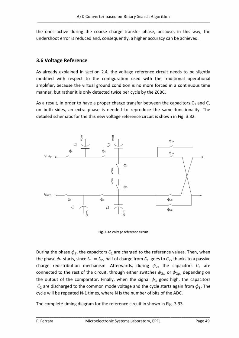
A/D Converter based on Binary Search Algorithm ____________________________________________________________________________________________________________
_______________________________________________________________________________ F. Ferrara Microelectronic Systems Laboratory, EPFL Page 49
the ones active during the coarse charge transfer phase, because, in this way, the
undershoot error is reduced and, consequently, a higher accuracy can be achieved.
3.6 Voltage Reference
As already explained in section 2.4, the voltage reference circuit needs to be slightly
modified with respect to the configuration used with the traditional operational
amplifier, because the virtual ground condition is no more forced in a continuous time
manner, but rather it is only detected twice per cycle by the ZCBC.
As a result, in order to have a proper charge transfer between the capacitors C1 and C2
on both sides, an extra phase is needed to reproduce the same functionality. The
detailed schematic for the this new voltage reference circuit is shown in Fig. 3.32.
Fig. 3.32 Voltage reference circuit
During the phase , the capacitors are charged to the reference values. Then, when
the phase starts, since , half of charge from goes to , thanks to a passive
charge redistribution mechanism. Afterwards, during , the capacitors are
connected to the rest of the circuit, through either switches or , depending on
the output of the comparator. Finally, when the signal goes high, the capacitors
are discharged to the common mode voltage and the cycle starts again from . The
cycle will be repeated N-1 times, where N is the number of bits of the ADC.
The complete timing diagram for the reference circuit in shown in Fig. 3.33.

A/D Converter based on Binary Search Algorithm ____________________________________________________________________________________________________________
_______________________________________________________________________________ Page 50 Microelectronic Systems Laboratory, EPFL F. Ferrara
Fig. 3.33 Time diagram for the reference circuit

A/D Converter based on Binary Search Algorithm ____________________________________________________________________________________________________________
_______________________________________________________________________________ F. Ferrara Microelectronic Systems Laboratory, EPFL Page 51
Chapter 4
Simulations & Results
4.1 Functional Simulations
In this first section of the Chapter, functional simulations are provided in order to check
the correct functionality of the single blocks and, finally, the functionality of the whole
architecture.
The first block to be tested is the above mentioned ZCBC, which replaces the Op-Amp
functionality by using a comparator and two current sources for each side of the fully
differential configuration. In Fig. 4.1 and Fig. 4.2, the results for the functional
simulations are presented. The capacitors are set to 500fF, the input signal is a sine wave
with a peak-to-peak amplitude of 1.6 V and the sampling frequency is set to 1MHz.
Fig. 4.1 shows the differential input (blue) and the differential output (red) of the ZCBC.
Fig. 4.1 Input and Output voltage of ZCBC
Furthermore, Fig. 4.2 shows the detailed behavior of the inputs( and ) and the
outputs ( and ) of the ZCD. Note that the signal directly controls the
switching on/off phase of the current sources in E2, whereas for , a small extra-
logic circuit is needed.

A/D Converter based on Binary Search Algorithm ____________________________________________________________________________________________________________
_______________________________________________________________________________ Page 52 Microelectronic Systems Laboratory, EPFL F. Ferrara
Fig. 4.2 Input and Output voltage of ZCD
After the functionality of the ZCBC was confirmed, a functional simulation for the whole
architecture was performed. The capacitor values are kept to 500fF and the same input
signal is used. The sampling frequency is lowered to 166,6 KHz, since the voltage
reference circuit is added to ZCBC. Thus, nine more cycles were required for each
sampled input value to determine the output code. In Fig. 4.3, the differential input (red)
and the differential output (blue) of the ZCBC are shown.
Fig. 4.3 Input and Output of ZCBC with voltage reference circuit

A/D Converter based on Binary Search Algorithm ____________________________________________________________________________________________________________
_______________________________________________________________________________ F. Ferrara Microelectronic Systems Laboratory, EPFL Page 53
From Fig. 4.3, it can be noticed how the voltage references are added to or subtracted
from the initial value of the output, depending on the result of the comparison
(cmp). A detail of the comparison operation is shown in Fig 4.4. The two differential
outputs ( and ) and the cmp signal (red) are represented. Note that the cmp
signal which goes high or low, depending on the values of (fuchsia) and
(green), setting the addition or the subtraction of voltage references for the next cycle.
Fig. 4.4 Detail of Comparison
4.2 Performance Simulations
The ADC was implemented as a 10 bits converter. The results of the performance
simulations are summarized in the following table (Table 4.2). The sampling frequency
was set to 166 kS/s and a sine wave with a peak-to-peak amplitude of 1.6V was applied
to the inputs. In order to have a coherent sampling, as already explained in section 3.15,
the input frequency was set to 16.4388kHz.
Note that the Figure of Merit (FOM) in the table, is computed with the following
formula:
(4.1)
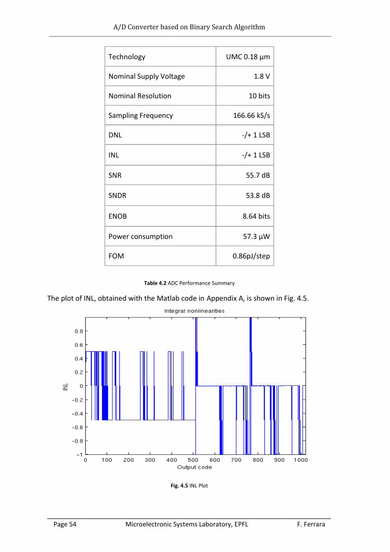
A/D Converter based on Binary Search Algorithm ____________________________________________________________________________________________________________
_______________________________________________________________________________ Page 54 Microelectronic Systems Laboratory, EPFL F. Ferrara
Technology UMC 0.18 µm
Nominal Supply Voltage 1.8 V
Nominal Resolution 10 bits
Sampling Frequency 166.66 kS/s
DNL -/+ 1 LSB
INL -/+ 1 LSB
SNR 55.7 dB
SNDR 53.8 dB
ENOB 8.64 bits
Power consumption 57.3 µW
FOM 0.86pJ/step
Table 4.2 ADC Performance Summary
The plot of INL, obtained with the Matlab code in Appendix A, is shown in Fig. 4.5.
Fig. 4.5 INL Plot

A/D Converter based on Binary Search Algorithm ____________________________________________________________________________________________________________
_______________________________________________________________________________ F. Ferrara Microelectronic Systems Laboratory, EPFL Page 55
The plot of DNL, obtained with the Matlab code in Appendix A, is shown in Fig. 4.8.
Fig. 4.6 DNL Plot
The spectrum of the quantized signal is given in Fig. 4.5, with the number of samples of
Fig. 4.7 Spectrum of Quantized Output

A/D Converter based on Binary Search Algorithm ____________________________________________________________________________________________________________
_______________________________________________________________________________ Page 56 Microelectronic Systems Laboratory, EPFL F. Ferrara
The ADC simulated transfer curve compared with an ideal transfer curve of an 10 bits
ADC is given in Fig. 4.6.
Fig. 4.8 ADC Transfer Curve
Analyzing the results from Table 4.2, it can be observed that the ADC nominal resolution
may be decreased from 10 to 9 bits, since the ENOB is 8.64. Therefore, the last shift
register of the SAR logic can be removed and the sampling frequency can be increased
from 166.6 kS/s to 185 kS/s, since is unnecessary to perform the last cycle of
comparison. As a consequence, the FOM will become smaller, assuming that the ENOB
remains approximately constant.

A/D Converter based on Binary Search Algorithm ____________________________________________________________________________________________________________
_______________________________________________________________________________ F. Ferrara Microelectronic Systems Laboratory, EPFL Page 57
Chapter 5
Conclusions & Future Perspective
In this report, the comparator based switched capacitor technique was implemented in
a Binary Search ADC in 180nm UMC standard CMOS technology. The proposed
architecture eliminates the need for an Op-Amp in the circuitry and replaces its
functionality with a combination of a comparator and current sources to realize the
same charge transfer. This technique was used because it is more suitable for
technology scaling.
All the analog building blocks of the ADC were implemented at a transistor level and
simulated. Furthermore custom modifications were provided for some blocks to
increase accuracy.
Afterwards, the whole ADC architecture was implemented using a sampling frequency of
166 kS/s and performance simulation results were presented in Table 4.2. The converter
reaches 8.64 bits of accuracy, with a SNDR = 53,8 dB and consumes 60 µW of power.
This performance is still not comparable with performance obtained with traditional Op-
Amp, in fact, according to [2], the power consumption of a BSA ADC using a cascoded
Op-Amp is 2 µW at 100 kS/s (measured on a chip) with a power supply of 1.2 V ( CMOS
0.13 µm technology). However, some further modification can be done in the design to
improve the ENOB and reduce the power consumption. For instance, since the highest
power consuming block remains the ZCBC, reducing a bit the slope of the current ramps
in phase E1 will result in an overall reduction of power consumption, without affecting
the sampling frequency which was not pushed to the limit. A further improvement could
be ZCD offset compensation. As explained in Chapter 3, traditional techniques for offset
cancelation cannot be used since the offset in ZCDS is dynamic and not static, but a
derivative technique, as explained in [4], can be implemented, increasing the accuracy
and the performance of the detector.
Finally, it would be interesting to implement the same architecture in a more scaled
technology (i.e. UMC 90 nm CMOS Technology), where the design of traditional Op-
Amps poses more difficult challenges, in order to check how technology scaling affects
the performance of ZCBCs and if they can be actually considered as an alternative
configuration to Op-Amps in Binary Search ADCs.

A/D Converter based on Binary Search Algorithm ____________________________________________________________________________________________________________
_______________________________________________________________________________ Page 58 Microelectronic Systems Laboratory, EPFL F. Ferrara

A/D Converter based on Binary Search Algorithm ____________________________________________________________________________________________________________
_______________________________________________________________________________ F. Ferrara Microelectronic Systems Laboratory, EPFL Page 59
Acknowledgement
The presentation of this report is the occasion to thank Prof. Alexandre Schmid for giving
me the opportunity to work in the Microelectronic Systems Laboratory (LSM), on such as
an interesting and challenging project. I would especially like to thank my supervisor
Nikola Katic for the time he spent to follow my project and for providing me all the help
and the guidance I needed. Furthermore, I would like also to thank Alberto Rodriguez
Perez for giving precious advices and for his constant encouragement.
Finally, I would like to express all my gratitude to my family for supporting me
throughout my whole studies and for having always been close to me even in the
distance.

A/D Converter based on Binary Search Algorithm ____________________________________________________________________________________________________________
_______________________________________________________________________________ Page 60 Microelectronic Systems Laboratory, EPFL F. Ferrara

A/D Converter based on Binary Search Algorithm ____________________________________________________________________________________________________________
_______________________________________________________________________________ F. Ferrara Microelectronic Systems Laboratory, EPFL Page 61
References
- [1] Zou X., Xu X., Yao L., Lian Y., A 1-V 450-nW Fully Integrated Programmable
Biomedical Sensor Interface Chip, IEEE journal of Solid-State Circuits (2009),
44(2):1067-1077.
- [2] Rodriguez-Perez A., Delgado-Restituto M., Medeiro F., Power Efficient ADCs
for Biomedical Signal Acquisition, 10: 171-191.
- [3] Northrop R. B., Non invasive Instrumentation and Measurements in Medical
Diagnosis, CRC Press LCL (2001).
- [4] Brooks L., Lee H.S., A 12b, 50 MS/s Fully Differential Zero-crossing Based
Pipelined ADC, IEEE journal of Solid-State Circuits (2009), 44(12), 329-343.
- [5] Fiorenza J.K., Sepke T., Holloway P., Charles G. Sodini, Lee H.S., Comparator-
Based Switched-Capacitor Circuits for Scaled CMOS Technologies, IEEE journal of
Solid-State Circuits (2006), 41(12), 2658 – 2668.
- [6] Gulati K., Ultra-Low Power Op-Amp less ADCs, Cambridge Analog
Technologies, (2011).
- [7] Pelgrom M.J.M., Analog to digital conversion, Springer (2010).
- [8] Dessouky M., Kaiser A., Input switch configuration suitable for rail-to-rail
operation of switched op-amp circuit, Electronics Letter (2011) ,35(1),8-9.
- [9] Abo A.M., Gray P.R., a 1.5V, 10 bit, 14MS/s CMOS Pipeline Analog-to-Digital
Converter, IEEE journal of Solid-State Circuits (1999), 34(5), 601-602.
- [10] Byunghank Cho T., Gray P.R., A 10b, 20 MS/s, 35 mW Pipeline A/D
Converter, IEEE journal of Solid-State Circuits (1995), 30(3), 166-170.
- [11] Jacob Baker R., CMOS Circuit Design, Layout and Simulation, Wiley-IEEE
Press (2010).
- [12] Lillebrekke C., Wulff C., Ytterdal T., Bootstrapped Switch in Low-Voltage
Digital 90nm CMOS technology.

A/D Converter based on Binary Search Algorithm ____________________________________________________________________________________________________________
_______________________________________________________________________________ Page 62 Microelectronic Systems Laboratory, EPFL F. Ferrara
- [13] Graupner A., A Methodology for the Offset-Simulation of Comparators,
(2010).
- [14] Rodriguez-Perez A., Ruiz-Amaya J., Delgado-Restituto, Angel Rodriguez-
Vasquez, A low-Power Programmable Neural Spike Detection Channel with
Embedded Calibration and Data Compression, IEEE Transactions on Biomedical
Circuits and Systems (2012), 6(2), 87-99.
- [15] Rossi A., Fucili G., Non redundant successive approximation register for A/D
converters, Electronics Letters (2006), 32(12), 1055-1057.
- [16] Keh K.-L., Kemna A., Hosticka B.J., Modular low-power high-speed CMOS
Analog-to-Digital Converter for embedded systems, Kluwer Academic Publishers
(2003).
- [17] Kester W., High Speed Sampling and High Speed ADCs, Norwood (1996).
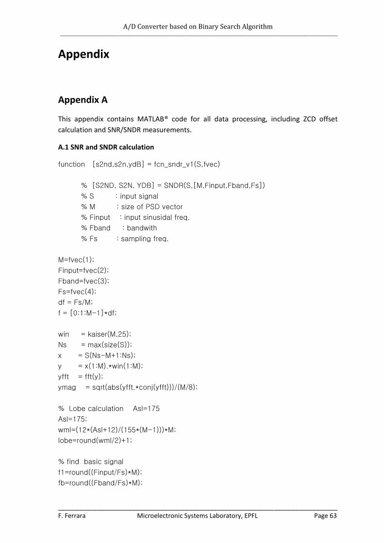
A/D Converter based on Binary Search Algorithm ____________________________________________________________________________________________________________
_______________________________________________________________________________ F. Ferrara Microelectronic Systems Laboratory, EPFL Page 63
Appendix
Appendix A
This appendix contains MATLAB® code for all data processing, including ZCD offset
calculation and SNR/SNDR measurements.
A.1 SNR and SNDR calculation
function [s2nd,s2n,ydB] = fcn_sndr_v1(S,fvec)
% [S2ND, S2N, YDB] = SNDR(S,[M,Finput,Fband,Fs])
% S : input signal
% M : size of PSD vector
% Finput : input sinusidal freq.
% Fband : bandwith
% Fs : sampling freq.
M=fvec(1);
Finput=fvec(2);
Fband=fvec(3);
Fs=fvec(4);
df = Fs/M;
f = [0:1:M-1]*df;
win = kaiser(M,25);
Ns = max(size(S));
x = S(Ns-M+1:Ns);
y = x(1:M).*win(1:M);
yfft = fft(y);
ymag = sqrt(abs(yfft.*conj(yfft)))/(M/8);
% Lobe calculation Asl=175
Asl=175;
wml=(12*(Asl+12)/(155*(M-1)))*M;
lobe=round(wml/2)+1;
% find basic signal
f1=round((Finput/Fs)*M);
fb=round((Fband/Fs)*M);
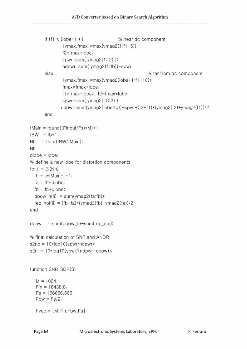
A/D Converter based on Binary Search Algorithm ____________________________________________________________________________________________________________
_______________________________________________________________________________ Page 64 Microelectronic Systems Laboratory, EPFL F. Ferrara
if (f1 < (lobe+1 ) ) % near dc component
[ymax,fmax]=max(ymag2(1:f1+5));
f2=fmax+lobe;
spwr=sum( ymag2(1:f2) );
ndpwr=sum( ymag2(1:fb))-spwr;
else % far from dc component
[ymax,fmax]=max(ymag2(lobe+1:f1+10));
fmax=fmax+lobe;
f1=fmax-lobe; f2=fmax+lobe;
spwr=sum( ymag2(f1:f2) );
ndpwr=sum(ymag2(lobe:fb))-spwr+(f2-f1)*(ymag2(f2)+ymag2(f1))/2
end
fMain = round((Finput/Fs)*M)+1;
fBW = fb+1;
Nh = floor(fBW/fMain);
Nh
dlobe = lobe;
% define a new lobe for distortion components
for jj = 2:(Nh)
fh = jj*fMain-jj+1;
fa = fh-dlobe;
fb = fh+dlobe;
dpow_h(jj) = sum(ymag2(fa:fb));
rep_noi(jj) = (fb-fa)*(ymag2(fb)+ymag2(fa))/2;
end
dpow = sum(dpow_h)-sum(rep_noi);
% final calculation of SNR and ANDR
s2nd = 10*log10(spwr/ndpwr);
s2n = 10*log10(spwr/(ndpwr-dpow));
function SNR_SDR(S)
M = 1024;
Fin = 16438.8;
Fs = 166666.666;
Fbw = Fs/2;
Fvec = [M,Fin,Fbw,Fs];

A/D Converter based on Binary Search Algorithm ____________________________________________________________________________________________________________
_______________________________________________________________________________ F. Ferrara Microelectronic Systems Laboratory, EPFL Page 65
[s2nd,s2n,ydB] = fcn_sndr_v1(S,Fvec);
s2nd
s2n
ydB(1:M/2);
freq_range = 0:Fs/(M-1):Fs/2;
figure (1)
subplot(2,1,1)
plot(freq_range,ydB(1:M/2));
title('Spectrum of Quantizer Output')
xlabel('f in [Hz]')
ylabel('Amplitude in dB')
end
A.2 ZCD Offset Calculation
function ZCDoffset (x, ydata)
M1=sum_up(ydata);
M=M1.';
y=sum(M)/100;
figure(1)
subplot(2,1,1)
plot(x,y);
title('Result of MonteCarlo simulation: cumulative hystogram');
xlabel('xi[V]');
ylabel('ni/N');
xdata=x.';
v=sqrt(2)*erfinv(y(1:512)*2-1);
i=find (v>-10 & v<10);
p=polyfit(xdata(i),v(i),1);
subplot(2,1,2)
plot(xdata(i),v(i),xdata(i), polyval(p,xdata(i)));
title ('Normal probability plot')
xlabel('xi [V]');
ylabel('ni/N');
sigma=1/p(1);
mu=-p(2)/p(1);
end

A/D Converter based on Binary Search Algorithm ____________________________________________________________________________________________________________
_______________________________________________________________________________ Page 66 Microelectronic Systems Laboratory, EPFL F. Ferrara
function matrix=sum_up(V1)
for k=1:100
for j=1:512
matrix(j,k)=V1(j+512*(k-1));
end
end
A.3 INL and DNL Calculation
function INL (in,out)
x=0:1:1023;
x1=reshape(x,1024,1);
y=(-0.8):0.6/1023:0.8;
y1=reshape(y,1024,1);
[p,s] = polyfit (y1,x1,1);
plot(in(1:1024),out(1:1024),y1,polyval(p,y1),'r');
title('ADC transfer curve')
xlabel('Input voltage')
ylabel('Output code')
figure(2)
stairs(in(1:1024),out(1:1024));
figure(3)
stairs(y1,polyval(p,y1));
for i=1:1024
inl (i)= -(out(i)-p(1)*in(i)-p(2));
end
figure (4)
plot(out(1:1024),inl);
title('Integral nonlinearities')
xlabel('Output code')
ylabel('INL')
end
function DNL (in,out)
s=0;
for i=1:1024
if (out(i+1)>out(i))
dnl(i) = -(out(i+1)-out(i)-1-s);
s=0;

A/D Converter based on Binary Search Algorithm ____________________________________________________________________________________________________________
_______________________________________________________________________________ F. Ferrara Microelectronic Systems Laboratory, EPFL Page 67
else
s=s+0.5;
dnl(i)=0;
end
end
figure (1)
plot(out(1:1024),dnl(1:1024));
title('Differential nonlinearities')
xlabel('Output code')
ylabel('DNL')
end
Appendix B
This second appendix contains the Verilog-A code for all data acquisition and processing,
necessary in order to evaluate ADC performances.
B.1 Output code acquiring for 10 Bits ADC
// Verilog-A for ADC data acquiring
`include "constants.vams"
`include "disciplines.vams"
module sample_bits (CLK_BITS, BITS);
input CLK_BITS;
input [0:9] BITS;
electrical CLK_BITS;
electrical [0:9] BITS;
integer s_BITS [0:9]; // sampling bits values
real OUT; // Output decimal value calculated from the bits
integer filedesc;
integer i;
analog
begin
@(initial_step) //file opening
begin
if (analysis("tran"))
begin
filedesc=$fopen("/home/fferrara/data.csv","a");
end
end

A/D Converter based on Binary Search Algorithm ____________________________________________________________________________________________________________
_______________________________________________________________________________ Page 68 Microelectronic Systems Laboratory, EPFL F. Ferrara
if(analysis("tran"))
begin
@(cross( V(CLK_BITS) - 0.9, 1))
begin
for (i=0, i<10; i=i+1)
begin
s_BITS[i] = ( V(BITS[i]) > 0.9) ? 1 : 0;
end
OUT=0;
for(i=10; i>0; i=i-1)
begin
OUT = OUT + s_BITS[i- 1]*pow(2,i-1);
end
$fstrobe(filedesc, OUT);
end
end
@(final_step) // file closing
begin
if(analysis("tran"))
begin
$fclose(filedesc);
end
end
end
endmodule
B.2 Data acquiring for ZCD offset estimation
// VerilogA for Monte-Carlo simulation
`include "constants.vams"
`include "disciplines.vams"
module data_monte_carlo (CLK, Vout, Vin);
input CLK;
input Vout;
input Vin;
electrical CLK;
electrical Vout;
electrical Vin;
integer fileDesc;
integer fileDesc1;
real sampling_CLK;
real sampling_Vout;

A/D Converter based on Binary Search Algorithm ____________________________________________________________________________________________________________
_______________________________________________________________________________ F. Ferrara Microelectronic Systems Laboratory, EPFL Page 69
real sampling_Vin;
analog
begin
@(initial_step)
begin
if (analysis("tran"))
begin
fileDesc =$fopen("/home/fferrara/ydata.csv","a");
fileDesc1=$fopen("/home/fferrara/xdata.csv");
end
end
if (analysis("tran"))
begin
sampling_CLK = V(CLK)-0.9;
@(cross(sampling_CLK, +1))
begin
sampling_Vout = ( V(Vout) > 0.9) ? 1 : 0;
sampling_Vin = V(Vin);
$fstrobe(fileDesc1, sampling_Vin);
$fstrobe(fileDesc, sampling_Vout);
end
end
@(final_step)
begin
if (analysis("tran"))
begin
$fclose(fileDesc);
$fclose(fileDesc1);
end
end
end
endmodule
B.3 Ladder-shaped input for offset calculation
`include "constants.vams"
`include "disciplines.vams"
module ladder (clk, Out );
input clk;
output Out;
electrical clk;
electrical Out;

A/D Converter based on Binary Search Algorithm ____________________________________________________________________________________________________________
_______________________________________________________________________________ Page 70 Microelectronic Systems Laboratory, EPFL F. Ferrara
parameter real Vamplitude=0.1;
parameter integer N=256;
parameter real stepsize= Vamplitude/N;
integer i,hold,h;
analog begin
@(initial_step) begin
i = 0;h = 0;
end
@(cross(V(clk),+1))
begin
hold = i;
if(i <= N && h != 1)
begin
i = i+1;
if(i == N)
begin
h =1;
end
end
else
begin
i = i-1;
if (i==0)
begin
h=0;
end
end
end
V(Out) <+ hold*stepsize+0.85;
end
endmodule