Embed Size (px)
Citation preview

U.S. DEPARTMENT OF COMMERCE National Technical Information Service
AD-A029 451
TECHNOLOGY AND PHYSICS OF INFRARED AND POINT
CONTACT DIODES
MASSACHUSETTS INSTITUTE OF TECHNOLOGY
JUNE 9. 1976

$1CHH0I.0GY ÄUD PHYSICS OF INFRARED
AND POINT CONTACT DIODES
Department of Physics Massachusetts Institute of Technology
Cambridge, Mass. 02139
Approved for Public Release» distribution unlintited.
Sponsored by Defense Advanced Research Projects Age*jcv
ARPA Order No. 2618
ROMS AIR DEVELOPMENT CENTER AIR ItmCE SYSTEMS COMMAND
PIS ;JR FORCE BASE, NEW YORK 1344 REPRODUCED BY
NATIONAL TECHNICAL INFORMATION SERVICE
U. S. DEPARTMENT OF COMMERCE SPRINGFIELD, VA. 22161
-IMP W&SSilt QfeWWOf DMPBS
.©at« of amttt
»^^ioi ©f WorlE. Covered J
auury If?i ■f^y '.JAY*/
^&e»i -417^Sl-«f37
Th« vieiRB and conclumivm eontmKnaä ia this doouasnt ar© author» and sbould not im intai^ratad as r«^r«««rntiag the official polic^asf ©ithsr
or dap-Hma, sf Mie Dafansa Advaacad Basaarch •jact« Äf«ncy or .t^» o.s. dovarnaant«
tMe xaport has haan ravi©«?ed fcy th® SÄDC Information ©ffiw (0£) and is raiaasafel« to a» national «aehnioaä lafoxmation Sarviee imtS), *t WKS it will ba ralaas« ahla to tha yenaral rohlic including foreign nations.
rapart has fecan ravi«isd and Is apprevad for publi-
Coatract Honitor
»ot ««tarn this mm* »stain or dastzoy.

Unclassified MIL-STD-8a7A 31 January 1973
IICUMITV Cl.»'-SIHC»T.:S 0' TM'S »fit '»IM Ptlt fn--.-J'
REPORT DOCUMENTATION PAGE I. lltPOKT NUMUF.R
RADC-TR ^76^234
;. OOVT »CCISSION hO
4. TlTLC tmna Svbhllt)
Technology and Physics of Infrared and Point Contact Diodes
7. *UTH0Äf»
Ali Java
KRAD INSTRl'CTIC'NS nK.FOKL COVrt.t.TtNO KCHM
I. HECiPlEN T'S CAT ALQi NJWÖtn
J. TYPE OF TPORT < PERIOD C0VEPE0
1 Nov. 75-30 Apr Scientific Interim t PEPFORMINC ORG "EPOPT NUMBER
Semi-Annnal Technika
». PCRFORHINC ORGANIZATION NAME AMD ADDRESS
Department of Physics Mass. Inst. of Tech., Cambridge
Ma. 02130
t. CONTRACT or, GRANT NUMBtRf<J
F19628-74-C-0182
II. CONTROLLING OFFICE NAME ANO ADDRESS
Defense Advanced Research Proj. Agency - 1400 Wilson Blvd. Arlington VA 72209 ,
M. HONlTORtrTC AOVNCV NAM£ * AOORESSfd ditfrttnt horn Confuting OUie9>
Deputy for Electronic Technology (RADC(ETSL))f Hanscom AFB, MA 0173 Contract Monitor: Audun Hordvik U OISTRISUTION STATEMENT (ol iMa Ktpcl)
10. PROGRAM ELEMENT. PROJECT, TASK AREA » «ORK UNIT NUMBERS
2001-01-01 61101E
U REPORT DATE
June 9. 1976 11 NÜMBCR OF PAGES
ü IS. SECURITY CLASS, (ol Ihlt rtpcrt)
Unclassified IS«. OECLASSIFICATION DOWNGRADING
SCHEDULE
Approved for public release; distribution unlimited
17. OISTRISUTION STATEMENT (ol in« mbtttocl tnltfd In Block 20, 11 dllloionl Horn Roporl)
I« tUPPLEMENTART NOTES
This Research was sponsored by the Defense Advanced Research Projects Agency, ARPA Order 2618
19- KEY WORDS 'Conrinu* on ttvt»9 aid« if n«r*i««ry «nd idrnitfv bit bincJr number)
Tunneling resonances, dielectric formation, oxide studies, photoernission.
20 ABSTRACT cConf/nu# on rovorjo «id« It ll«c«f«*V ond idvnn/v *y btock nuirttr)
Repair work on our liquid helium has been success- fully completed, A pump and pumping lines have been installed which enable us to pump the helium to cool it helo 7 the lambda point and perform our experimental work in superfluid helium .
76
I Report #4
DO I JAN"?! M73 EDITION OF 1 NOV»» II OBSOLETE Unclassified SCCURITV CLASSIFICATION OF THIS I-AGE (»Inn D«(« rnffdl
Report Documentat ion Page.
PRICES SUBJECT TO CHANGE

M1L-STD-8U7A 31 January 1973
Unclassified «CCU'lTr CU«SSIflC«T|g>| 0f THIS P»OE»h.o n.,. tn,.„4
Cont. Block #20
A tube and mirrors have been installed from the argcjn and dye laser room to the diode testing area. This permits greater availability of the laser and more working space near the beams.
Additional lead on aluminum diodes were evaluated at liquid helium temperature. Interpretation of these and earlier runs indicates:
a. For low non-saturating power levels from RF through visible, junction responses at low bias (les than 20 mv) were identical.
b. For higher biases with the junction in superfluid helium, resonances were not detectable at frequencies above RF. However, a constant offset from zero was observed (opposite senses for opposite biases) which seemed to increase with increasing radiation frequency. This is taken as an indication of photoresponse for electrons overcoming the super- conducting gap.
An oxidation study was conducted on nickel which demonstrated that 400 square micrometer junctions from 100 ohms through 1 megohm can be made. Those junctions are moderately stable over a few days in room ambient. Lead on tin junctions have been made in the few kilohm range.
Real time V-band and 337 vim holographic receptors have been designed and masks are being fabricated.
Measurements are in progress on MOM (tungsten on nickel) point contact diodes to evaluate their effective antenna resistance as a function of length. The effective diode resistance is varied b^ changing whisker pressure and response is maximized with respect to whisker orientation in the focused laser beam. Antenna resistance is obtained by ad- justing parameters on a curve of diode resistance versus rectified voltage.
Jlnc lafLsili^d.
™J
SeCU**tTV CLASSlTlCATtO*« OF 'MtS PAGE'H*» D*i» t.nfrmd)
11

TABLE OF CONTENTS
pa^e
1. Summary 1
2. Introduction 3
3. Dewar Repair 4
4. Superfluid Helium 4
5. Extension of Laser Lab 4
6. Low Temperature Response of
Al-Al203-Pb Junctions 5
7. Metal Oxidation Techniques 7
8. Mask Fabrication 8
9. Point Contact Antenna Resistance 8
PiiL are 1 10
Fief are 2 11
Fig are 3 12
111

-1-
1. SUMMARY
Repair work on our liquid helium dewar has been
successfully completed. A pump and pumping lines have
been installed which enable us to pump the helium to cool
it below the lambda point and perform our experimental
work in superfluid helium„
A tube and mirrors have been installed from the argon
and dye laser room to the diode testing area. This permits
greater availability of the laser and more working space
near the beams.
Additional lead on aluminum diodes were evaluated at
liquid helium temperature. Interpretation of these and
earlier runs indicates:
a. For low non-saturating power levels from RF through
visible, junction responses at low bias (less than 20 mv) were
identical.
b. For higher biases with the junction in superfluid
helium, resonances were not detectable at frequencies above
R F. However, a constant offset from zero was observed
(opposite senses for opposite biases) which seemed to in-
crease with increasing radiation frequency. This is taken
as an indication of photoresponse for electrons overcoming
the superconducting gap.
An oxidation study was conducted on nickel which demon-
strated that 400 square micrometer junctions from 100 ohms
through 1 megohm can be made. Thei-e junctions are moderately
stable over a few days in room ambient. Lead on tin junctions

, i
-2-
have been made in the few kilohm range.
Real time V-band and 337 ym holographic receptors
have been designed and masks are being fabricated.
Measurements are in progress on MOM (tungsten on nickel)
point contact diodes to evaluate their effective antenna
resistance as a function of length. The effective diode resistance
is varied by changing whisker pressure and response is maximized
with respect to whisker orientation in the focused laser beam.
Antenna resistance is obtained by adjusting parameters on a
curve of diode resistance versus rectified voltage.

-3-
INTRODUCTION
Preliminary work in this laboratory has shown that
tunneling characteristics of metal-oxide-metal junctions
are essentially independent of frequency as long as photon
energy is less than the barrier height. Recent calculations
show the effects of circuit parameters on response of an-
tenna/diode combinations; the junction capacitance is re-
sponsible for roll off in the infrared. Capacitance reduction
requires shrinking junction size, hence the need for micron
and submicron geometries. Photo emission (over the barrier
rather than tunneling) and thermal effects dominate the
response in the visible region. It seems likely that photo-
emission is a fast effect and can be used for visible
mixing.
Important elements of device merit are junction non-
linearity and even negative resistance which may be enhanced
by choice of materials, techniques of application and op-
erating temperature.

-4-
3. DEWAR PEP;.';
Our liquid helium dewar has been repaired and used in
a number of low temperature runs. This dewar is equipped
with quartz windows in each of three ports and has in the
past been subiact to failure seemingly at the most criti-
cal times. The manufacturer found three leaks, one of
which occurred only at low temperature. Repair has per-
mitted us to make our runs with no problem from the dewar,
and only routine pump downs of the vacuum chamber.
4. SUPERFLUID HELIUM
In an attempt to maintain junctions under test at a
constant temperature the helium in the dewar was pumped.
After increase in the size of the pumping line and of the
pump, it became possible to pump the liquid helium to be-
low the lambda point in about 40 minutes. Although there is
a thermal match barrier between the junction and the helium
subsequent work has demonstrated that superfluid helium
(below the lambda point at 2.1° K) does maintain the sample
at a much more uniform temperature than "normal"liquid
helium.
5. EXTENSION OF LASER LAB
A tube and sets of mirrors have been installed from the
argon and dye laser room to the diode testing area. This has
permitted much greater availability of the argon laser and

-5-
considerably increased working space near the laser beams.
6. LOW TEMPERATURE RESPONSE OF Al-Al^-Pb JUNCTIONS
Rectification characteristics of Al-Al-O-j-Pb junctions
were studied at 4020K (liquid helium) and 20K (helium pumped
below the lambda point). In both cases the lead was super-
conducting and the aluminum was "normal." Measurements
were made at 10 MHz, x-band (microwave), 337ym (HCN laser)
and with laser light in the visible.
The junctions were made by evaporating a 20 ym wide
strip of aluminum to a thickness of 500 8, oxidizing it in
a few torrof pure oxygen for half an hour and then evap-
orating a thick 20 ym wide strip of lead across the oxidized
aluminum. Resistances at 50 mV DC ranged from a few hundred
to a few thousand ohms. RF was coupled to the junctions by
the leads through the dewar top while the higher frequencies
were beamed through the dewar windows.
In the low bias (0-20 mv) region responses to low inten-
sity radiation of all wavelengths were the same. The super-
conducting transition at about 1.5 mv as well as phonon mode
excitations were observed. (See Fig. 1) Widths and positions
of each resonance were the same. Power saturation occurred
for laser powers greater than one milliwatt. Similar saturation
was observed with RF and at X-band.
At biases greater than about 20 mv and temperatures be-
low the lambda point, tunneling resonance responses to visible

-6-
laser radiation could not be detected, however there was an
offset from zero which is roughly constant with bias voltage
but has the same polarity as the applied bias. (See Fig. 2)
Qualitatively, this response seemed to increase with increasing
radiation frequency and it is taken as an indication of photo-
response for electrons overcoming the superconducting gap.
At temperatures above the lambda point, the effect of the
resonances is to give a distorted bell curve. Since these
observations are made with mechanically chopped radiation
and amplified with coherent detection on a lock-in, this
appears to be the difference between normal tunneling response
at two different temperatures.
Lead on aluminum diode response to 10 MHz radiation was
observed at 4.2 K in the presence of argon laser radiation.
It was observed that one mw. of radiation detectably reduced
ehe structure of the 10 MHz pattern whereas 100 mw reduced it
to less than 10%. Sensitivity of the response due to super-
conducting characteristics of lead was only slightly more
reduced than the high field anomalies.
The model we currently use to explain these observations
is that superfluid helium maintains the junction at nearly
the same temperature, with and without radiation so that
I-V curves are nearly parallel. But above the lambda point
the heating causes considerable temperature rise with con-
sequent broadening of the resonance; the lock-in displays the
difference of these two curves.

Very little X-band power is coupled through the windows
into the dewar. This is not enough to observe the higher
bias resonances. However, the I-V characteristics due to
the superconducting gap, at about 1,5 mV are extremely
sharp and maKe the junction a very sensitive detector;
these resonances have been seen at X-band despite the very
low incident power level.
7. METAL OXIDATION TECHNIQUES
To study oxidation characteristics of nickel, several
20ymx20 pm junctions were fabricated. Nickel was evaporated
first and the slide heated on the hot plate. Four runs gave
the following resistances as a function of oxidation time.
Junction Oxidation Time Resistance Range
Ni-NiO-Pb 0 hours short
Ni-NiO-Pb 3 hours 81ß - 130 fl
Ni-NiO-Ni 4 hours 68Ch2 - 910^
Ni-NiO-Pb 15 3/4 hours 320 Kfi-900 KQ
Resistances typically increased by a quarter in the 24 hours
following their preparation.
A lead on tin junction was made with three hours of hot
plate oxidation. Resistances were 4.3 Kfi and 8.2 Kß. They
increased by half in the 17 hours after fabrication. This
junction should be operable in the high microwave region
and as a negative resistance device below 3.50K.

8. MASK FABRICATION
A real time V - band holographic receptor war designed,
rubylith cut and sent out to be photoreduced. Masks have
been made for photo production. Units were started but it
was discovered that there was lack of metal adherence for the
lift off step. We have found that glow discharge cleaning
is required before metal deposition; parameters were varied
and 200 pm of oxygen for 5 minutes at 2 mA seems a good
first approximation. Substrates must be clean, but no
special initial surface preparation appears necessary when
the glow discharge is used. Some exposure problems seem
to be present due to reflection from the substrate holder
of the mask aligner. This will be corrected with a black
anodized holder, in fabrication.
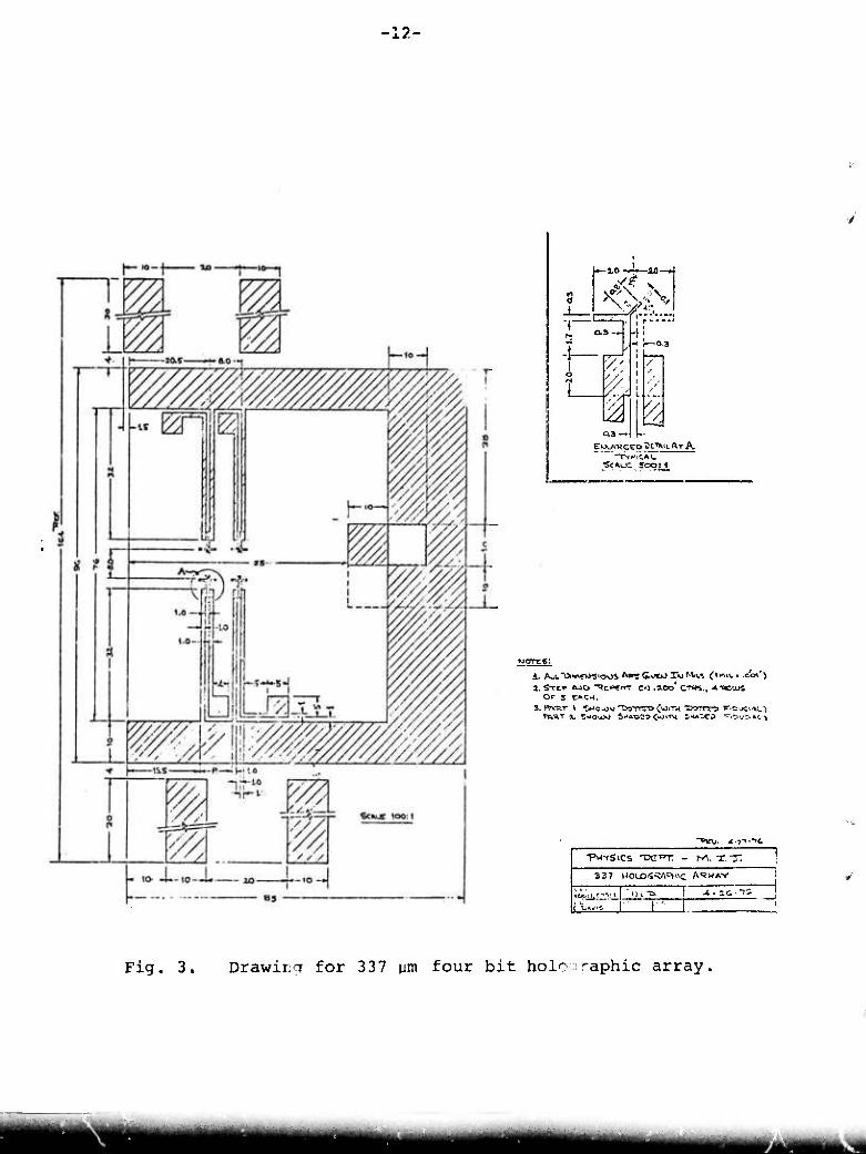
A four element holographic sensor mask for 337 pm
work has been designed and is being fabricated. (See Fig. 3)
9. POINT CONTACT ANTENNA RESISTANCE
Measurements are in progress on MOM (tungsten on nickel)
point contact diodes to evaluate their effective antenna re-
sistance as a function of length. The 10 ym diameter tungsten
whisker acts as a multiwavelength antenna with effective
antenna resistance of R . The tunneling barrier presents a
junction resistance of Rd at the DC bias voltage. The
point is small enough that we can neglect capacitive effects
so that the voltage rectified across the diode is:

A value of Ra can be determined by adjusting param ',ers
on a curve of Rd vs. Vd.
A characteristic of thin dipole antennas is that the
capture cross section has resonances near nX /2 (integral
values of n). The antenna resistance for very long antennas
is 163 ß .
Antenna resistances were calculated for various length
whiskers with 337 ym radiation from the HCN laser. This
radiation was focused onto the junction region of the diode
with a teflon lens. The rectified signal was then maximized
by adjusting orientation to the peak of the largest antenna
lobe. Rd is varied by changing the diode contact pressure on
the nickel post. To maintain a constant tunneling barrier
height, all data for an R, calculation must be taken without a
moving the whisker on the nickel post.
The experimental results for long antennas (longer than
about 5 A )are in agreement with the theoretical expectations
(Ra ~ 160 Ü ). Data for other antenna lengths are still being
taken and evaluated.

Fig. 1
X- Band radiation
5145 A argon laser radiation
Al-Al50,-Pb diode responses at liquid helium temperature
{20K) in the low bias region. (0-20 mv). The argon
radiation was adjusted to make first satellite peaks of
the same height. Jn both cases, the radiation was below saturation.

-.2
^V^U^v.
\
0 .4V
5145Ä argon laser radiation at 6mW
Fig. 2. Al-AljC^-Pb diode responses in superfluid liquid helium
at biases to ±0.4V. The laser focus is centered on the
20 pro square junction. The vertical at zero bias is due to
the superconducting transition. Note that the offset
approaches a constant value for bias greater than 0.1V.
-12-
d
T
A-
( r----
//,
W n
Or s c«CH.
"Pmj, ^o"»-"»^
■PKTSics 'DET»r - M. XT: '
337 VJOLOSSftOH'C ft*"*««" j
IBlCMtfT^»M ■■u"3- i JI-IU--:' ! jji^o I- 1
Fig. 3. Drawing for 337 ym four bit holo;raphic array.

c* tßfzuwt&^wt&Kßnü^jp*^^
MISSION of
Rome Air Dewhjnmnt Center
RADC plans and nducts research, exploratory and advanced drrelopment program in cosamnd, control, and commnications (C3) {activities, anil in the C3 areas of information sciences and intelligence. The principal technical mission are«« are commmications, electromagnetic guidance and control, surveillmce of ground and aerospace objects, intelligence data collection and handling, information systen, technology, ionospheric propagation, solid state sciences, microwave physics and el'nctronic reliability, maintainability and compatibility.
t&*ßnit#*#WK0*j&*j^j*^^
Piint«d bj* United Stat«s Air Fore« Hanseon AFB, Mot«. 01731
^13