Embed Size (px)
Citation preview

UNCLASSIFIED
AD 2 8 8 5333
Al'•MI') SEIRVI(CES TFClIHNICAL INFORMATION AGENCYAlRIJN(,TON HALL STATIONAIRILING;TON 12, VIRGINIA
1J NCLASS][FIED

NOTICE: When government or other drawings, speci-fications or other data are used for any purposeother than in connection with a definitely relatedgovernment procurement operation, the U. S.Government thereby incurs no responsibility, nor anyobligation whatsoever; and the fact that the Govern-ment may have formulated, furnished, or in any waysupplied the said drawings, specifications, or otherdata is not to be regarded by implication or other-wise as in any manner licensing the holder or anyother person or corporation, or conveying any rightsor permission to manqufrt.xre, l2ie or sell Fny
patented invention that may in any way be relatedthereto.

28.8533Ci-JOR OFFICIAL. USE ONLY
100
R 214Tech vical Report THE TWO CURRENT-PROBE METHOD OF
......... MEASURING CONDUCTED RADIO-
............ FREQUENCY INTERFERENCE
28 September 1962
U ..... ... AA II NINEIGLBRTR
PoOctm, atfrk
... NO...OTS

THE TWO CURRENT-PROBE METHOD OF M•ASURING CONDUCTED RADIO-FREQUENCY INTERFERENCE
Y-F006-09-205
Type B
by
James L. Brooks
ABSTRACT
A new approach to the problem of measuring conducted interference is described.A brief discussion is presented on the limitations and uncertainties of the presentlyaccepted method using Line-Impedance-Stabilization Networks (LISN). These limita-tions stem from the fact that no information is obtained concerning the impedancevalues of the circuit being measured during a noise measurement. The new methoddescribed provides a means of overcoming the limitations of the present methodcompletely by the use of commercially available current-probes in an impedance-and noise-measurement system.
A method of determining the impedance values of the circuit has been workedout which requires the use of two current-probes. E-itler he noise-source impedanceor the load impedance or both may be determined by this method. Two separatemeasurements and calculations are required however, one to determine the magnitudeof the impedance and the other to determine the phase angle.
An evaluation of the device is -resented, as well as numerous examples ofnoise measurements showing the correlation between measured and predicted results.
The precision of the impedance-measuring system is within 20 percent throughoutthe frequency range of 2 to 3? megacycles where phase angle is measured for most ofthe commonly encountered line and source impedance values. For measurement ofimpedance magnitudes, the accuracy of the system is better than 20 percent for therange of the current-probes (100 kilocycles to 100 megacycles).
Qualified requesters may obtain copies of this report from ASTIA.The Laboratory invites comment on this report, particularly on the
results ob+ained by those who have applied tho information.

INTRODUCTION
The project is concerned with providing a better method for performing RFIacceptance tests on equipment such as electric motors, transmitters, etc., procuredby the Bureau. The present method as set forth by Mil-1-16910A using line-impedance-stabilization networks leaves considerable doubt as to the true value of the conductedRFI existing on the power connections of the equipment tested.
Since electrical noise may be narrow band or broadband in nature, and maybeeither radiated or conducted from the source, the instruments used to monitor thenoise-voltage levels are highly sensitive frequency-selective devices with outputmeters calibrated in microvolts across a specified input impedance of 50 ohms. Itis mandatory that the input impedance remain constant in order to maintain goodcalibration over the frequency band of the instrument.
Unfortunately, when used as a two-terminal voltmeter in the LISN measurement,the low impedance of the meter presents considerable loading to circuits of higherimpedance levels. A high-impedance blocking network such as the line-impedance-stabilization networ'k is presently used to isolate the device under test from its powerconnection and provide a known load across the line.
PROBLEM ANALYSIS
Given: An electrical or electronic device which is to be tested for conductedradio interference to determine its acceptability.
Figure 1 shows the schematic. It is the purpose of this test to determine thenoise voltage (Vn).
deviresea cunder
test
Figure 1. Electrical noise and current on power cord.

The device under test may be replaced by an equivalent noise source andimpedance (Figure 2).
zz Vz
Figure 2. RF equivalent circuit of device under test.
where V = equivalent noise-source voltages
Z - equivalent noise-source impedancce5
T = noise current on the power cordn
S= noise voltage across the power cord at point of measurementn
ZL = equivalent load impedance of the power outlet
The circuit equations are:
V 5 1T z s+ V nIS n s n
n n L (2)
n S ZS
L
2

PRESENT METHOD
It is apparent that connecting the RFI meter across the line as a two-terminalvoltmeter would load the circuit and yield unreliable readings, particularly whenthe source impedance and load impedances are greater than 50 ohms. For this reason"a different approach has been taken.
The usual method for making conducted interference measurements is to insert"a network into the line which will effectively block out the load impedance andprovide a known impedance for the noise source to work into. These networks havebeen designed, are available commercially, and are called line-impedance-stabilization networks. The circuit diagram of a typical line-impedance-stabilizationnetwork is shown in Figure 3.
Zp""1 f
501 TTLFigure 3. Line-Impedance-stabilizotion network.
The noise voltage (VA) measured with the noise ,,,er in this circuit is of coursenot the voltage that would appear on the line with the network removed, due to theloading effect of this network on the device under test. As a matter of fact, thevoltage measured in this manner gives no indication at all as to what voltage wouldactually appear )n the line with the network removed since the noise-source impedanceand the load impedance are normally not known. The best that can be done with thisLISN is to say that the voltage measured is at least repeatable for identical hookupsand to record the readings as induced voltages into the LISN. The equivalent circuitusing the LISN is similar to that for the normal situation,, as shown in Figure 2, withthe exception of the load impedance, which is now 50 ohms (see Figure 4).
3

nn
Figure 4. RF equivalent circuit with LISN inserted.
The circuit equation for this situation is:
n= V s (4)
S1 R
It is obvious that unless the normal load impedance ZL happens to be 50 ohmsthe voltage reading across the LISN will not be the correct voltage existing on theline in the normal situation. The voltage difference may be represented vectorilyas shown in Figure 5.
nV
n
V
Figure 5. Vector diagram showing the difference between thenormal noise voltage (9n) and the noise voltagemeasured using a LISN (Vn).
4

The vector difference Vn - Vn is clearly a function of the impedances of thecircuit and will henceforth be called the error voltage. An investigation into thepossible range of the error voltage is now in order.
The quantities Zs and ZL are both physical impedances and as such may rangein magnitude from 0 to co and from -90 to +90 degrees in phase angle. Thereforethe quantity Zs/ZL may range from 0 to co in magnitude and from -180 to +180 degreesin phase angle. Also the quantity Z,/R may range from 0 to co in magnitude but onlyfrom -90 to +90 degrees in phase angle.
It immediately becomes apparent that the term I/[l + (Zs/ZL)] which appearsin Equation 3 may possess a discontinuity when Zs/ZL =-1; otherwise it is well-bounded. However the quantity 1/[I + (Zs/R)] from Equation 4 does not possessdiscontinuities and is well-bounded between 0 and 1.
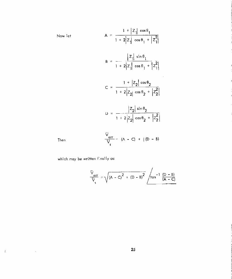
The equation for the error voltage may be written as:
- - 1n _5)
err n Z Z (5)1+ ZL i+R
As pointed out above, the first term of the error voltage equation possesses adiscontinuity at Zs/ZL = -1 which represents a maximum error situation. Figure 6shows a plot of the error equation, as derived in Appendix A.
The following significant points to be derived from Figure 6 are:
1. The discontinuity occurs at Zs/ZL = -1 at 180 degrees.
2. There is only one discontinuity point.
3. The error due to phase angle is only appreciable when 0. 1 < Zs,/ZL < 10.
4. The error voltage due to differences in magnitude alone of the impedanceswill not exceed Vs.
5. The probability of occurrence of the point of discontinuity is extremelysmall. This point requires a simultaneous occurrence of i'wo independently improbablesituations before the error voltage can approach infinity: (a) the impedance-magnituderatio must be exactly equal to 1; and (b) the phase angle of the ratio must be exactly180 degrees.
5

C C
-K� K- � N
NiN 77 1--I> ILilij 0) 7J
_____ 4- 0_______ I>' UP __ 0 -
I/fl - 4-0)
/if�f-V
*,4 1> 4- �
__ -4 _---------___
- -�-----
-40 0* I
0) �
Ii Ou,- I -A--l�
I- --- H Ill
-� 14 0)0)
- -, >0
* I
'00)
__-]
U..
N NI
CO cCC 0
I>�I I>'
6
The second requirement for the discontinuity point is even more improbablethan the first since it requires impedances which possess infinite Q's, or in otherwords, pure reactive values. As stated before, the actual impedances possess acertain amount of resistance, which in turn lowers the Q of the circuits, thereforelowering the maximum error voltage. This resonnce effect is shown by the familyof curves in Figure 6.
For the foregoing reasons, the presently accepted method of measuring conductedinterference is unsatisfactory. No information concerning impedance values in thecircuit is obtained during a measurement, resulting in considerable inaccuracy of thereadings. Hence a different approach to the measurement problem was taken. It istherefore the object of this task to develop a circuit or circuits that can provide ctrue indication of conducted interference from the variety of electrical items beingtested for RFI.
CONTRACT WORK AND REPORT
This Laboratory contracted with the Stoddart Aircraft Radio Corporation,Los Angeles, to investigate the possibilities of using the two current-probe methodof measuring conducted RFI and impedance and to build a prototype instrument forthis purpose.
The work performed by the contractor is described in detail in his final report.*The high points of that report will be mentioned here.
The contract requireme:nts were:
1. To study and evaluate presently used line-impedance-stabilization networksand new networks now in production or being proposed.
2. To investigate new techniques of measuring conducted interference usinuthe Stoddart current-probe and probes for measurement of interference and RFimpedances of noise sources.
3. To make interference and impedance measurements as necessary to obtainsupporting data when such data was not otherwise available.
4. If comparison and correlation studies disclosed a need for new techniques,and/or devices for the measurement of conducted interference, recommendationsrelative thereto should be given to the fullest extent practicable.
• Stoddart Aircraft Radio Co., Inc. Improved Line Impedance Stabiliza'ion Method,
by J. W. Show and E. R. Byerley. Hollywood, Calif., October 1960.
7

The contractor conducted a literature search into the many phases of conducted-interference-measurement techniques used in the past as well as the presently acceptedmethods. This search pointed out the following disadvantages of the presently acceptedmethod of measuring conducted interference with LISN networks:
1. The four-terminal impedance-stabilization network must be inserted intothe noise-carrying line.
2. This insertion is likely to change the actual noise current flowing in theline because of a concomitant change of circuit parameters.
3. The physical size of the 5-microhenry choke limits the power-current levelat which the impedance-stabilization network may be used.
Significant work performed by the Naval Material Laboratory at New YorkNaval Shipyard, Brooklyn, was described. A dual and single line-impedance-stabilization network were designed, which made it possible to measure conductedradio interference up to 100 megacycles with repeatable results. The dual unit waslimited to 5 amps, the single unit to 50 amps.
The contractor proposed a new method for measuring conducted interference;however the analysis presented in the contract report is incomplete and difficult tofollow. Therefore a simpler approach is presented. This method can best be explainedby returning to the noise-source equivalent circuit in Figure 2. A review of thecircuit equations shows that the noise voltage Vn could be determined easily if Inand ZL were known. The system to be described here makes it possible to determinethese values by utilizing commercially available current-probes.
The assumption is made that even though the quantities Vs, Vn, and In arebroadband in nature, when measured with a narrow-bandwidth instrument, they willdisplay c-w (continuous-wave) characteristics and will be treated accordingly. Asa direct result of this, the impedances involved will have a bandwidth dependenceassociated with them; however, they too will be treated as normal c-w impedances.Unless resonances in the impedance characteristics occur, the impedance changewithin the RFI-meter bandwidth will be small.
The noise current In may be measured directly, as shown in Figure 7. Thecurrent-probe reflects a constant low impedance into the circuit and thereforegenerally yields accurate readings.
8

Z n ZL
noise meterAN/PRM-1 detector
Figure 7. Measurement of noise current T.
The equivalent load impedance ZL can be measured as shown in Figure 8.
Z T
: n
Z
V
sinaV noise meter
SgeneraVto2 AN" PRM.1 detector
Figure 8. Measurement oF load impedance ZL.
This circuit may be redrawn as shown in Figure 9.
noise meter
signalAN,/PRM-1 detector
generator
Figure 9. RF equivalent circuit for measuring ZL.
9)

The equation for the impedance ZL as derived from this configuration in Appendix Bis:
1z- I (6)
where K is the noise-meter impedance reflected into the measuring circuit.
The noise voltage Vn existing across the impedance ZL of the line may nowbe determined by the equation
IV TIJZL 1(7)
The noise-source voltage Vs may be determined in a similar manner by firstmoving the shorting capacitor to the dotted-line position (see Figure 8) and measuringI Z.1. Once IZsI is determined, Tn may be measured for this new situation and Vsdetermined by the relation IVs TnIjZs.
Based on the above theory, a prototype instrument was built; the features were:
1. The impedance-magnitude-measuring capability is limited by the current-probe transfer impedance which has a 3-db bandwidth of 0. 5 to 45 megacycles.
2. The impedance-magnitude-measurement accuracy is within 20 percentwhen averaged values for K are used in Equation 6, or better than 10 percent whena V1/V2 versus frequency nomograph is used in the computations (see Figure 10).
3. The power-current-carrying capability is 350 amps ac or dc.
4. The instrument is constructed entirely of passive circuitry.
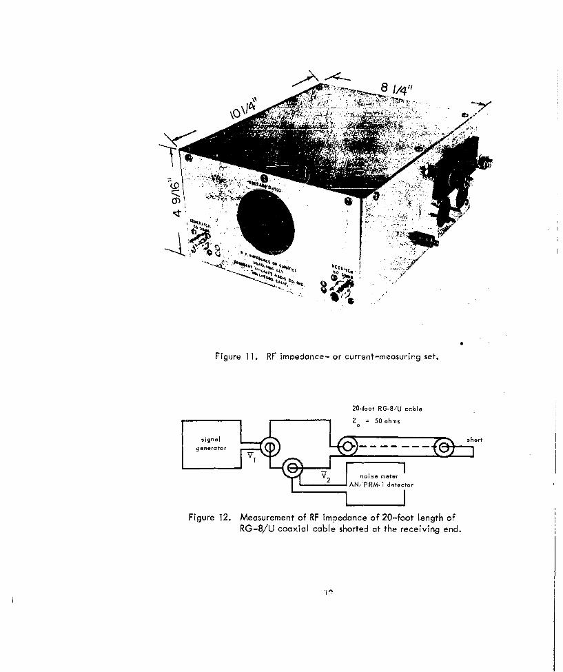
5. A photograph of the instrument is shown in Figure 11.
The contractor measured the impedance of various electrical networks andnoise sources. An example of one of those tests is shown in Figure 12. In this testa 20-foot length of coaxial cable was shorted on one end by a Type N shortingtermination; the other end was used to form a small loop for coupling the probes.
10

10000- - - 100A
1000__
1 002 4 6 8 1 2 1 4 1 8 2 2 268 2 8
Frqec 1me50yies
Fiue1.Ln-meac esrn-eieipdnevrufrqec2nmgah
125
48/
"Lt'.A% i- t07
ell
Figure '11. RF impoedance- or current-measuring set.
20-foot RG-B/U cable
signal coxascbesoreotthreetiged

The results of the impedance measurements of the shorted 20-foot coaxial cable(Figure 13) showed the anticipated resonances.
The contractor also performed extensive measurements on a three-phase powerdistribution system associated with Radio Telegraph Transmitting Equipment ModelTBK-17. This particular transmitter is capable of putting out 500 watts on c-wtransmission from 2 to 18 megacycles. The impedance of the line (plus load) variedwith frequency from 3000 ohms (maximum) to 30 ohms (minimum). Resonances, asindicated by points of high or low impedance, occurred at the same respectivefrequencies whether impedances were measured in a single phase or between twophases. For a single-phase measurement, both probes were connected around thesame conductor and separated by only a small distance. For measurements betweentwo phases, a probe was placed around each conductor of the two phases involved.This necessitated a large physical separation of the two probes. Impedances measuredbetween two phases were about seven times those measured in one phase of the three-phase line due to the large separation of the current-probes.
The contractor performed numerous tests on the following noise-producingequipment:
1. A c-w interference source
2. An ac-dc rotary converter
3. A universal motor
From the values measured, the equivalent noise-source voltage and potentialpower output of the noise sources were calculated and correlated with presently usedmethods involving LISN. In addition, the amount of interference which would beconducted into a particular 60-cycle power-line connection was calculated andcorrelated with measured results. All measured and calculated values agreed closely,indicating this system of interference measurement was useful in measuring andpredicting noise voltages.
It was found that measurement of impedance of the universal motor should bemade only when the armature is spinning. Ideally, the test-sample motor shaftshould be rotated by another motor at the rated speed of the test-sample motor.Preliminary measurements indicated however that the speed of shaft rotation is notimportant.
13

4000 ..... t
1000 -li
10 100 300
Frequency (megacycles)
Figure 13, Curve of impedance measurements of shorted 20-foot coaxial
cable (I to 105 megacycles).
14

The contractor made the following general observations concerning his workand results.
It is very important to note that at present this is the only known method ofmeasuring impedance in a closed-loop circuit where no connections must be broken.Examples of some practical applications of this would be antenna-impedance measure-ments while operating, and power-line-impedance measurements where large currentsare flowing.
When measuring power-outlet RF impedances, care must be taken to insure thatthe signal generator and noise meter used are not plugged into the same line undertest since this may alter the impedance being measured.
When test equipment did cause changes in the power-outlet impedance, it wasusually the result of large filter capacitors connected across the power-line input tothe equipment. Equipment that did not possess these capacitors only affected the lineimpedance slightly.
The impedances of normal power-line connections vary widely from a few ohmsto several thousand ohms depending on the frequency of measurement, loc'ation of thepoint of measurement, line characteristics, and line terminations.
There will exist several resonances and anti-resonances on the average powerline, the extent of which will depend upon the relationship of the factors justmentioned.
Although interference correlations and validity using the new techniques (onthe test samples cited above) have been established, other types of test samples shouldbe correlated. Examples of additional test samples are receivers, transmitters, dia-thermy equipment, and other electronic equipment.
Therefore it might be final;y stated that the practical improvement limit andrange of applications have not yet been ascertained.
CONTRACT WORK EVALUATION AND IMPROVEMENT AT NCEL
When the contract terminated in October 1960, the contractor submitted hisfinal report and prototype instrument to this Laboratory. At that time a conferencewas held with the engineers who had worked on the project to discuss the possibilitiesof improving the measurement device. The principle improvement discussed was thatof developing supporting instrumentation for the device to provide information aboutimpedance phase angles in addition to the impedance magnitude already provided.
15

As a result of this conference it was determined that a study should be made bythe Laboratory to determine the usefulness of information concerning the impedancephase angles by investigating the possible range of errors involved when phaseinformation is not used.
This task was undertaken and the answer to the question concerning the usefulnessof phase-angle information is presented in this report under Problem Analysis. Thedevelopment of a method and circuitry for obtaining phase information has been accom-plished and will be explained in the remainder of this report.
A method has been developed which permits the determination of the phase angleof the noise-source or load impedance utilizing the impedance setup previously described(Figure 8) in conjunction with a continuously variable-delay line and step attenuator.The setup is described in Figure 14.
Sdelay atteni
Sline uotor •_
' • i gnS1
Figure 14. Measurement of both magnitude and phase of theunknown impedance (Z L6).
In this setup, the input signal is divided into two paths. The primary path isthe normal impedance-magnitude-determination circuit. The second path is thecomparison path. The magnitude of the impedance is determined in the same manneras before by reading V1 and V2 and calculating Z. Then S1 is closed, and the com-parison path is adjusted until the voltage V2 + V3 = 0, indicated by a n.,l cn •ienoise meter. The delay-line time setting is read to obtain the total delay time atnoise-meter null. This delay time is then compared to the time reading obtainedusing a pure resistance of the same magnitude as Z. The phase deviation is thencalculated from the difference in the time readings (see Appendix C).
At =t - t
9 = At (360) wherelT
or 9 = Atf (360) (8)
16

With this technique the impedance of the noise source and load can be specifiedas to magnitude and phase angle. The noise voltage itself may be indirectly measuredas previously explained. Once these quantities have been completely specified, it ispossible to predict the noise voltage and power delivered by the noise source to anyknown load impedance.
Based on the above consideration, the contractor's current-probe impedance-measuring device was modified by the addition of the components outlined in theblock diagram of Figure 14. A photograph of the device after modification is shownin Figure 15. The large double dial on the upper left is the control knob for thedelay line and is calibrated in microseconds. It is this dial which is read for the timesettings.
Figure 15. Modified impedance-measuring device.
17

The modified instrument now has the following performance features:
I. The impedance-magnitude-measuring capability is limited by current-probetransfer impedunce which has o 3-db bandwidth of 0.5 to 45 megacycles.
2. The impedance-magnitude-measurement accuracy is within 20 percent whenaveraged K values ore used in Equation 6, or better than 10 percent when a V1/V2versus frequency nomograph is used in computations.
3. The phase-angle-measuring capability is limited from 2 megacycles to30 megacycles. The lower-frequency limitation is due to the total delay of thedelay line which is 0.5 microseconds. The higher-frequency limitation is due rc:poor response of the delay line above 30 megacvcles.
4. The accuracy of the phase-angle measurements is ±20 percent trom 2 t,30 megacycles for impedance magnitudes greater than 30 ohms. For impedancumagnitudes less than 30 ohms the accuracy becomes progressively worse.
5. The power-current-carrying capability is 350 amps ac or dc
6. The instrument is constructed entirely of passive circuitry.
EXPERIMENTAL RESULTS OF IMPEDANCE-MAGNITUDE AND PHASE-ANGLEMEASUREMENTS
As a practical test of the ability of the device to reasule phase angles, numerousfrequency-dependent load impedances were inserted across the load terminals of thedevice and measured. These measured values were then plotted along with theimpedance-bridge-measurement values of the loads. Tvo examples of the results ofthese tests are shown in Figures 16 and 17,
The next test performed on this device was to measure the source impedances of,arious electric motors. As indicated by the contractor's work, the impedance ofanything which is connected by a length of line will vary with standing waves on theline, depending of course on the length of the line and frequency of measurementAn example of this is shown in Figure 18.

(s~aajr6p) Qj 5uV asno~-Q:)uopadwjj
InI
000

(sooJ60P) 06u'V QsDL~d-a~uDpodwI
7 (N
C3C
I C4
C))
lx.>)
ID _ _ _ _ _ _
-v CL
E -
-viF
Isqo appft )uoe
200

CN
E
131
7t
211

An evaluation of the ability of the measurement system to predict the noisevoltage from an arbitrary source across a known load impedance was performed by:
1. Measuring the equivalent noise-source impedance of a 3/4-inch electricpower drill.
2. Measuring the equivalent noise-source short-circuit current.
3. Computing the equivalent noise-source voltage.
4. Computing the noise voltage which the noise-source equivalent circuitwill present across a 50-ohm load.
5. Measuring the noise voltage that the power driil presented into a 50-ohmLISN load.
6. Comparing the computed value oi noise voltage with the measured value.This test was run several times with satisfying results, an example of which is shownin Figure 19.
CONCLUSION
The two current-probe technique of measuring coriducteo radio-trequenuyinterference has demonstrated a considerable superiority over the present methodof measuring RFI with line-impedance-stabilization networks. The current-probetechnique, though it is more time-consuming in operotion, eliminates the ambiguitiesassociated with conducted-noise measurements.
RECOMMENDATI ONS
On the basis of the above conclusion, it is recommended that:
1. Further work be done to extend the useful frequency range of the instrument.
2. The two current-probe technique be incorporated into the Mil-l-16910Aspecification for measuring conducted RFI, in order to update and improve theconducted-RFI measurements being made in the Bureau of Ships and Bureau of Yardsand Docks.
22

I I)IIl
_____ ____
-4- -Ell
/u
C I I I I4LL
-j 3 ,-
o 23

Appendix A
DERIVATION OF CURVES PRESENTED IN FIGURE 6.
The ratio of the error voltage to the source voltage may be written as follows:
err _ 1
1+ 1+
ZL R
zLet Z e / Z=
ZL
z, 2 r2 R
Then Z1! e 1 =-Iz 11(cose 1 + sine@)
and Z2 / = Iz 2 j(cose 2 + sisne 2 )
By substitution and expansion
rr. -,+ Izil c•se1 -i Z sine
V s I + 2 Zj Cos 19 + 2
1 + Iz2j Cos2- iez2j sine 2
1 241 2 +
24
1 + IZl1 cos9 1
N ow let A = I + 2 IZI1 cos & 1 + 21
1 + 21Z 11 cos el + Iz21
1 + 1 Z21cos8 2
C I+ z212 Cose6 2C= Cos 9I• 2o0 + Iz"1 2
I z21 sine 2
1 + 2Z 2 cs 2 + 221
Verr (A - C) + (D-B)Then -
which may be written f:nolly as:
__________ //err F22 + (DB)2 -1 (D-B)
V - 7 \/(A _C ) a (A - C)
25
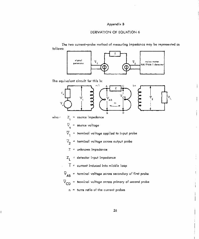
Appendix B
DERIVATION OF EQUATION 6
The two current-probe method of measuring impedance may be represented asfol lows:
sgeneato v• J VJ noise meter
genratr2 AN/PRM-1 detector
The equivalent circuit for this is:n:1 A C n
zzs
VCD 7Z2 L
AB D
V = source voltage
V' = terminal voltage applied to input probe
V2 = terminal voltage across output probe
Z = unknown impedance
ZL detector input impedance
T current induced into middle loop
VAB terminal voltage across secondary of first probe
VCD terminal voltage across primary of second probe
n - turns ratio of the current probes
26

Since the probes are identical and function in the circuit as transformers, theterminal-voltage relationships are:
VAB - -- (B-I)
2and VC (8-2)
CD n
The assumption wilI be made that the current-probes act as ideal transformers.
The impedance of the load (ZL) will then be reflected into the middle loopas a load for VCD as follows:
VC D =- T(-R (6-3)
n
The voltage relationships of the middle loop may now be written as:
V AB = 17 + VCD (B-4)
or, solving Equation B-3 for I and substituting,
V- ( 2VZD++ n ) +(B-5)
Substituting V1/n for VAB and V2 /n for VCD (as indicated by Equations B-i andB-2) into Equation B-5,
V--- 2 (n +B-6)
n n z2
27

Solving Equation B-6 for Z yields:
Z = L - ) (B-7)n 2
The quantity ZL/n2 by definition is a function of the detector and the probes used inthe circuit. For any given situation this ratio will be constant and will be definedas:
ZLK = z
2n
Unfortunately the detector used to measure V1 and V2 is only capable of measuringtheir magnitudes; therefore, Equation B-7 will be finally written as:
Z K (B-8)
28

Appendix C
DERIVATION OF EQUATION 8
In measuring the phase angle of the unknown impedance, the measuring systemis shown in block diagram form:
delay atten- j
line ua11or
signalv2nisIeegenerator AN/'PRM-1 detector
Figure 14. Measurement of both magnitude and phase of theunknown impedance (Z L8).
To measure the phase angle of the impedance (Z):
1. Measure the impedance magnitude j Zj in the normal manner.
2. Close switch (S1 ) and adjust both the delay line and attenuator simultaneouslyfor a null on the detector.
3. Record the final time setting on the delay line as t 1.
4. Replace the impedance with a resistor of magnitude R -Iz.
5. Readjust the delay line for a detector null. (The attenuator should notrequire readjusting.)
6. Record the new time setting on the delay line as t2 .
7. The phase angle 6 oF the impedance Z A is proportional to the timedifference between t1 and t 2 as indicated below.
e = (t1 - t2 ) (f) (360) degrees
29

This equation may be derived as follows:
By rewriting equation B-8, the outPut voltage of the secondary current-probeis:
V = zV_.0
K
Due to the inherent impedance of the particular circuitry used, it was found to beunreliable to use the comparison method for impedance magnitudes less than 30 ohms.Therefore the above equation will be simplified by making the following approximation:
zZi•If A 1K
where Z/8 > 1O
K:" 1
Then V2 " V
The voltage output of the comparison path circuit may be written as:
V3 = VIA 1
where Al ind*cotes magnitude and 01 indicates phase change. Then when the detectorindicates a null output with Z as the load,
-K c)V2 +V 3 =0 or V2 =V 3 or A 1 (C-)
30

When the detector indicates a null output with the resistor R = I as a load,
K
A '- R (C-2)
Solving Equatrion C-2 for K and substituting this into Equation C-i yields:
A, 2 Z / '/(A2!__02
or z R- R =2-)h
Since R fZz
and A2 - tA
then = 2 -Th
where c2 = Wt2
(Dt = ~tl
Then - 2-f (t2 - tl) radians (C-3)
To obtain degrees, Equation C-3 may be rewritten as:
e = (t2 - tl) (f) (360)
31

24 megacycles t .0558 ,s
22 megacycles 6.44 /840 10' t - .060 Ps
62 0 megacycles 5.83 /83 34' t .0665 ýts
18 megacycles 5.24 Z/2 50' t .073 Mus
51
16 megacycles 4.65 810 54' t - .011 its
Ill
a414 megocycles 40/80a 4 * . 02 1,-
S1 megacycles 3.57 /790 25' t .0164, Its
iif - 2.1 .8 1, .0200 "S
megacycles 2.12 //720_L t - .0360 .,s
2 1 1
-- a 6nmegacycles 1.8'5 /690 19' t .0322 ,s
5 megacycles 1.59 /650 34' t .0395 i's
4 megacycfes T.334 1600 35ý t - '.0414 .,'s
3 megacycle, 1.09 / 5 3 t .04 )us
2 megacycles .873 /41" 29' .04 js
t is delay-line time settingv I __ I0 1 2 3 4
R (ohms)
Figure 20. Internal-impedance magnitude and phase characteristics ofmeasuring circuit.
32

To obtain the phase angle of an impedance less than 30 ohms a differenttechnique must be used.
The problem arises from the fact that the coupling loop formed by thepower-line shorting capacitor and load has an inherent impedance which maybecome as large as 10 ohms at the higher frequencies (see Figure 20). This imped-ance will be called Zloop and must be corrected for in the following manner.
The time reading for the impedance of ZI___ is subtracted from the timereading of the impedance being measured. The angle between the two vectors isthen calculated from this time reading:
= (tI - t2 (f)(0360) (C-4)
The two impedances are then drawn on a vector diagram.
ZI Oa
The correct value of the impedance and phase angle is now determined by obtainingthe vector difference between Zm and Zloop:
•Zloop
\ZL
Zm
Fortunately, most of the commonly encountered impedances are greater than 30 ohmsand this correction is not necessary. When resonance conditions are encounteredwith the resultant high- or low-impedance values, measurement at these resonantfrequencies can be avoided. More accurate measurements at frequencies on eitherside of resonance can be made and the resonant impedances can be calculated.
33

DISTRIBUTION LIST
No. of SNDL
copies Code
10 Chief, Bureau of Yards and Docks (Code 70)
I 23A Naval Forces Commanders (Taiwan Only)
4 398 Construction Battalions
10 39D Mobile Construction Battalions
3 39E Amphibious Construction Battalions
2 39F Construction Battalion Buse Units
1 A2A Chief of Naval Research - Only
2 A3 Chief of Naval Operation (OP-07, OP-04)
5 A5 Bureaus
2 B3 Colleges
2 E4 Laboratory ONR (Washington, D. C. only)
1 E5 Research Office ONR (Pasadena only)
I E16 Training Device Center
7 F9 Station - CNO (Boston; Key West; San Juan; Long Beach; San Diego; Treasure Island;and Rodman, C. 7. only)
6 F17 Communication Station (San Juan; San Francisco; Pearl Harbor; Adak, Alaska; and
Guam only)
I F21 Administration Command and Unit CNO (Saipan only)
I F40 Communication Facility (Pt. Lyautey only)
I F41 Security Station
1 F42 Radio Station (Oso and Cheltanham only)
I F48 Security Group Activities (Winter Harbor only)
8 H3 Hospital (Chelsea; St. Albans, Portsmouth, Va; Beaufort; Great Lakes; San Diego;
Oakland; and Camp Pendleton only)
1 H6 Medical Center
2 J1 Adminirtration Command and Unit - BuPers (Great Lakes and San Diego only)
1 J3 U. S. Fleet Anti-Air Warfare Training Center (Virginia Beach only)
2 J4 Amphibious Bases
1 J19 Receiving Station (Brooklyn only)
1 J34 Station - BuPers (Washington, D. C. only)
1 J37 Training Center (Bainbridge only)
1 J46 Personnel Center
1 J48 Construction Training Unit
I J60 School Academy
I J65 School CEC Officers
1 J84 School Postgraduate
1 J90 School Supply Corps
34
Distribution List (Cont'd)
No. of SNDLcopies Code
1 J95 School War College
1 J99 Communication Training Center
11 LI Shipyards
4 L7 Laboratory - BuShips (New London; Panama City; Carderock; and Annapolis only)5 L26 Naval Facilities - BuShips (Antigua; Turks Island; Barbados; San Salvador; and
Eleuthera only)
I L30 Submarine Base (Groton, Conn. only)
2 L32 Naval Support Activities (London & Naples only)
2 L42 Fleet Activities . BuShips
4 M27 Supply Center
7 M28 Supply Depot (Except Guantanamo Bay; Subic Bay; and Yokosuka)
2 M61 Aviation Supply Office
15 N| BuDocks Director, Overseas Division
28 N2 Public Works Offices
7 N5 Construction Sattalirn Center
5 N6 Construction Officer-in-Charge
S N 7 Construction Resident-Officer-in-Charge
12 N9 Public Works Center
I N14 Housing Activity
2 R9 Recruit Depots
2 RIO Supply Installations (Albany and Barstow only)
1 R20 Marine Corps Schools, Quantico
3 R64 Marine Corps Base
I R66 Marine Corps Camp Detachment (Tongan only)
6 WIAI Air Station
33 W1A2 Air Station
8 WlB Air Station Auxiliary
4 WiC Air Facility (Phoenix; Monterey; Oppama; Naha; and Naples only)
4 WIE Marine Corps Air Station (Except Quantico)
1 Wi F Marine Corps Auxiliary Air Station
8 WiH Station - BuWeps (Except Rota)
I Deputy Chief of Staff, Research and Development, Headquarters, U. S. Marine Corps,Washington, D. C.
I President, Marine Corps Equipment Board, Marine Corps School, Quantico, Va.
I Mr. A. Goutos, Headquarters, European GEEIA (AFLC), UnIted States Air Force, APO 332, New Yorl
1 Mr. F. W. Farr, Transmission Design Section, U. S. Department of the Interior, Bonneville PowerAdministration, Portland, Ore.
35

Distribution List (Cont'd)
No ofcopies
I Chief of Staff, U. S .Army, Chief of Research and Development, Department of the Army,Washington, D. C.
Office of the Chief of Engineers, Assistant Chief of Engineering for Civil Works, Deportment ofthe Army, Washington, D. C.
I Chief of Engineers, Departme.nt of the Army, Attn: Engineering R & D Division, Washington, D. C.
I Chief of Engineers, Deportrment of the Army, Attn: ENGCW-OF, Washington, D. C.
I Director, U. S. Army Engineer Research and Development Laboratories, Attn: Information
Resources Branch, Fort Belvoir, Va.
I Headquarters, Wright Air Development Division, (WWAD-Library), Wright-Patterson Air ForceBase, Ohio
3 Headquarters, U. S. Air Force, Directorate of Civil Engineering, Attn; AFOCE.ES,Washington, D. C.
I Commanding Officer, U. S. Navy Yards and Docks Supply Office, U. S. Naval Construction
Battalion Center, Port Hueneme, Calif.
1 Deputy Chief of Staff, Development, Director of Research and Development, Department of the
Air Force, Washington, D. C.
1 Director, National Bureau of Standards, Department of Commerce, Connecticut Avenue,Washington, D. C.
2 Office of the Director, U. S. Coast and Geodetic Survey, Washington, 0. C.
i.g Armed Sarvices Technicnl Infarmatinn An- - Aringtcrn Half Station, Arlington, Va.
2 Director of Defense Research and Engineering, Department of Defense, Washington, D. C.
2 Director, Division of Plans and Policies, Headquarters, U. S. Marine Corps, Washington, D. C.
2 Director, Bureau of Reclamation, Washington, D. C.
I Fn-iliti-, Officer (Code 109) Oflir,,.. C. -,
I Cuomr..u.di,,t Uii , U, t.. i''." C-nstruction Battalion Center, Port Hueneme, Calif.,Atin; Materiel Department (Code 140i
2 Mr. Stanton Bennett, Officer in Charge of Construction, 1156 15th Street, N. W., Room 313,
Washington, D. C.
2 Bureau of Ships (Code 695-B), Department of the Navy, Washington, D. C.
1 Mr. Guy Johnson, Communications Department, U. S. Army Signal Research Dev. Lab.,
Fart Monmouth, N. J.
Mr. J. Fred Chappel, Communications Department, U. S. Army Signal Research Dev. Lab.,
Fort Monmouth, N. J.
1 Electronics Branch, Material Laboratory, U. S. Naval Shipyard, Brooklyn
1 Aeronautical Electronic & Electrical Laboratory, Naval Air Development Center, Johnsville, Pa.
I Headquarters, U. S. Air Force Security Service, San Antonio, Tex., Attn: Asst. Dir, Maintenance& Plant Engineering, DCS/Communications-Electronics (ESD)
5 Commanding Officer and Director, U. S. A~my Electronic Proving Ground, Fort Huachuca, A:'iz.,Attn: W. R. Foley
I Mr. Harold C. Hurlbut, Department of the Navy, Northwest and Alaskan Division, Bureau o4:Yards and Docks, 1638 West Lawton Way, Seattle, Wash.
36
Distribution List (Cont'd)
No. ofCopies
I Commandant, Industrial College of the Armed Forces, Washington, D. C.
1 Commandant, U. S. Armed Forces Staff College, U. S. Naval Base, Norfolk, Va.
1 Chief, Bureau of Ships, Attn: Chief of Research and Development Division, Navy Department,Washington, D. C.
I Officer in Charge, U. S. Navy Unit, Rennseloer Polytechnic Institute, Troy, N. Y.
I Chief, Bureau of Naval Weapons, Attn: Research Division, Navy Deportment, Washington, D. C.
I Commander, Pacific Missile Range, Attn: Technical Director, Point Mugu, Calif.
1 Officer in Charge, U. S. Naval Supply Research and Development Facility, Naval Supply Center,Bayonne, N. J.
1 Commander, U. S. Naval Shipyard, Attn: Material Laboratory, Brooklyn, N. Y.
1 Office of Naval Research Branch Office, Navy No. 100, Box 39, FPO, New York
1 Commanding Officer, Naval Electroni.s Laboratory, Attn: Technical Director, San Diego
1 Commanding Officer, Fleet Training Center, Navy No. 128, c 'o FPO, San Francisco
1 Deputy Chief of Staff, Research & Development Headquarters, U. S. Marine Corps, Washington, D. C.
1 Chief of Ordnance, U. S. Army, Attn: Research & Development Laboratory, Washington, D. C.
I U. S. Army, Attn: Director of Research and Development Group, Washington, D. C.
I President, Signal Corps Board, U. S. Army, Forr Monmouth, N. J.
1 Commanding Officer, Signal Corps Engineering Labs., Fort Monmouth, N. J.
1 U. S. Army Corps of Engineers, Office of the Dstrict Engineer, St. Paul District, 1217 U.S.P.O.onrl C,--t-m Hn-,- St P-,1 Minrin
f..i_| . €C. _li .k ,... f _J 0_ - ,
1 Air Force Cambridge Research Center, Hanscom Field, Bedford, Mass.
... . .......... _ .C " '. ---. ,.nur7 , nnorens Mm rarv Uu+,
1 Directorate of Research, Air Force Special Weapons Cente-, Kirtland Air Force Base, N. M.
i Sandio Corporation, Attn: Ciassified Document Division, Box 5•00, Albuquerque, N. M.
1 Chief, Physical Research Branch, Research Division, U. S. Department of Commerce, Bureau ofPublic Roads, Washington, D. C.
I HQ Western GEEIA Region, McClellan Air Force Base, Sýcramento, Calif., Attn: Z.S.M.E.G.
2 Deputy Director, Air Force, Electronic Compatibility & Analysis Center, Naval Engineering
Experiment Station, Annapolis, Md.
Deputy Director, Navy, Electronic Compatibility & Analysis Center, Naval EngineeringExperiment Station, Annapolis, Md.
37

0- L
0 1.0
0 0
4) 0- a, o .0jC
LL F 0 '137) "0 -u c~
Of a) a~ 0 t4)-0 V" " , 4
t) .20 -o 00~~~. O ( m 14
0- -4 a>L - - 2o r
0 0
D -0 0 O-
z2i 0a,- -0j tOznza -AL Z4 ID
0 c E O-C 0 l E~u, CC) C N 4)F
> u u04) > >.0 Z D > ov)
70 (D ' I- 72 -) 0 >Ca
< Q
a, no
C, 0
Cc" W -a0j
Z; o CN
da
~~~~o~0 EO ~ SI ' ,
:)i -0 z v-0 I z E 0 -0 c
v) u
C:~~~a a -m < L ", 2 0.c
0 ~41c4 (L j E -pA- 0
cIc C) 4