Embed Size (px)
Citation preview

ACTIVE CURRENT SHARING CONTROL
SCHEMES FOR PARALLEL CONNECTED
AC/DC/AC CONVERTERS
BASSIM M.H. JASSIM
A thesis submitted for the degree of
Doctor of Philosophy
2014
School of Electrical and Electronic Engineering
Newcastle University
United Kingdom

Declaration
i
Declaration
I declare that the thesis entitled
“ACTIVE CURRENT SHARING CONTROL SCHEMES FOR PARALLEL
CONNECTED AC/DC/AC CONVERTERS”
is the results of my own research except as cited in the references.
The thesis has not been accepted for any degree and is not concurrent submitted in
candidature of any other degree.
Abstract
ii
Abstract
The parallel operation of voltage fed converters can be used in many applications, such
as aircraft, aerospace, and wind turbines, to increase the current handling capability,
system efficiency, flexibility, and reliability through providing redundancy. Also, the
maintenance of low power parallel connected units is lower than one high power unit.
Significant performance improvement can be attained with parallel converters
employing interleaving techniques where small passive components can be used due to
harmonic cancellation.
In spite of the advantages offered by parallel connected converters, the circulating
current problem is still a major concern. The term circulating current describes the
uneven current sharing between the units. This circulating current leads to: current
distortion, unbalanced operation, which possibly damages the converters, and a
reduction in overall system performance. Therefore, current sharing control methods
become necessary to limit the circulating current in a parallel connected converter
system.
The work in this thesis proposes four active current sharing control schemes for two
equally rated, directly paralleled, AC/DC/AC converters. The first scheme is referred to
as a “time sharing approach,” and it divides the operation time between the converters.
Accordingly, in the scheme inter-module reactors become unnecessary, as these are
normally employed at the output of each converter. However, this approach can only be
used with a limited number of parallel connected units. To avoid this limitation, three
other current sharing control schemes are proposed. Moreover, these three schemes can
be adopted with any pulse width modulation (PWM) strategy and can be easily
extended to three or more parallel connected units since they employ a modular
architecture.
The proposed current sharing control methods are employed in two applications: a
current controller for three-phase RL load and an open loop V/f speed control for a
three-phase induction motor. The performance of the proposed methods is verified in
both transient and steady state conditions using numerical simulation and experimental
testing.

Dedication
iii
Dedication
To Hidden Imam Mahdi (A.S),
may God hasten his reappearance

Acknowledgements
iv
Acknowledgements
First of all, I am extremely thankful to the Ministry of Higher Education and Scientific
Research of Iraq, for awarding me a scholarship for my PhD studies.
I would like to express my sincere gratitude to my supervisors, Dr. Bashar Zahawi and
Dr. Dave Atkinson, for their guidance and support. I consider myself extremely lucky to
have had an opportunity to work under their supervision.
I would like to take this opportunity to express my deep appreciation to the faculty
members of the Electrical Engineering Department in Baghdad University for their
encouragement and assistance, especially Tagreed M. Ali, Sulaiman M. Abbas, Dr.
Sadiq Jassim, Ahmed Mohsen, Dr. Jafer Alwash, Enas Ibrahim, and Thamir Mousa.
A special acknowledgement must also go to all of my colleagues in Power Electronics,
Drives and Machines Research Group for their valued friendship and help during my
time at Newcastle University. I also need to show my appreciation of the staff of the
electronic, electrical, and mechanical workshops for their support.
I am also thankful to my parents, brothers, sisters, and my dearest nephew Taqi for their
support throughout my PhD. Last but not least, I offer my special appreciation to my
wife, who without her support and best wishes, I would not have come to the end of my
study.
Table of Contents
v
Table of Contents
Abstract ............................................................................................................................ ii
Dedication ....................................................................................................................... iii
Acknowledgements ......................................................................................................... iv
Table of Contents ............................................................................................................ v
List of Figures ................................................................................................................. xi
List of Tables .............................................................................................................. xxiii
List of Abbreviations ................................................................................................. xxiv
Chapter 1. Introduction .................................................................................................. 1
1.1 Motivation and objective .................................................................................... 1
1.2 Thesis contributions ........................................................................................... 2
1.3 Thesis outline ..................................................................................................... 3
1.4 List of publications ............................................................................................. 4
Chapter 2. Background and Literature Review ........................................................... 5
2.1 Voltage Source Inverter ...................................................................................... 5
2.2 Fundamentals of Symmetrical Components ....................................................... 5
2.3 Clark and Park Transform .................................................................................. 7
2.4 Pulse Width Modulation Strategies .................................................................... 9
2.4.1 Sinusoidal pulse width modulation ........................................................... 12
2.4.2 Space vector pulse width modulation ....................................................... 14
2.4.3 Discontinuous pulse width modulation ..................................................... 19
2.5 Current Control Techniques for a Three-Phase Voltage Source Inverter ........ 23
2.5.1 Linear current controllers ......................................................................... 24
2.5.2 Hysteresis current control ......................................................................... 26
2.6 Parallel Operation ............................................................................................. 26
Table of Contents
vi
2.7 Circulating Current and Cross Current: Definitions and Generation ............... 28
2.8 Interleaving Techniques ................................................................................... 32
2.9 Review of Control Methods for Parallel Connected Three-Phase Converters . 35
Chapter 3. Proposed Methods ...................................................................................... 39
3.1 Time Sharing Approach ................................................................................... 39
3.2 Average Current Sharing Control Scheme ....................................................... 40
3.2.1 Current sharing regulation analysis ......................................................... 41
3.2.2 Design of PI controller gains .................................................................... 46
3.3 Independent Current Sharing Control .............................................................. 49
3.3.1 Current sharing regulation analysis ......................................................... 50
3.4 Impedance Emulation Current Sharing Control Scheme ................................. 53
3.5 Summary .......................................................................................................... 55
Chapter 4. Simulation Results ..................................................................................... 57
4.1 Simulation of the PWM Strategies ................................................................... 57
4.1.1 SVPWM SIMULINK model ....................................................................... 57
4.1.2 DPWM SIMULINK model......................................................................... 63
4.2 Time Sharing Approach ................................................................................... 67
4.2.1 Simulation results of time sharing approach ............................................ 71
4.3 Average Current Sharing Control Scheme ....................................................... 76
4.3.1 Parallel connected converter current-controller based on the average
current sharing control scheme .............................................................................. 76
4.3.2 Open loop V/f control for three-phase induction motor supplied from
parallel converters based on the average current sharing control method ............ 83
4.4 Independent Current Sharing Control Scheme ................................................. 89
4.4.1 Parallel connected converter current-controller based on independent
current sharing control method .............................................................................. 89
4.4.2 Open loop V/f control for three-phase induction motor supplied from
parallel converters based on independent current sharing control scheme ........... 92
Table of Contents
vii
4.4.3 Independent current sharing control strategy applied to three units ....... 95
4.5 Impedance Emulation Current Sharing Control Scheme ................................. 97
4.5.1 Simulation results of parallel connected converter current controller
based on an impedance emulation current sharing approach ................................ 97
4.5.2 Simulation results for open loop V/f control for three-phase induction
motor supplied from parallel connected converters based on impedance emulation
current sharing control scheme ............................................................................ 101
4.6 Interleaving Impacts on System Performance ................................................ 103
4.6.1 Combined current ................................................................................... 103
4.6.2 Inter-module circulating current............................................................. 106
4.6.3 Common mode voltage ............................................................................ 107
4.7 Summary ........................................................................................................ 110
Chapter 5. Development of Parallel-Connected Converters System...................... 112
5.1 System Overview ........................................................................................... 112
5.1.1 System requirements................................................................................ 112
5.1.2 System structure ...................................................................................... 113
5.2 Hardware Implementation .............................................................................. 115
5.2.1 AC/DC/AC converter unit ....................................................................... 115
5.2.2 General purpose power interface board for the Texas Instrument®
TMS320F28335 DSP microcontroller .................................................................. 120
5.2.3 Test load .................................................................................................. 124
5.3 Implementation of control algorithms ............................................................ 124
5.3.1 LabViewTM
environment .......................................................................... 125
5.3.2 Algorithm of time sharing control scheme .............................................. 126
5.3.3 Algorithm of average current sharing control scheme in a current
controller application ........................................................................................... 128
5.3.4 Algorithm of open loop V/f control for three-phase induction motor
supplied from parallel converters based on the average current sharing control
scheme ................................................................................................................. 129
Table of Contents
viii
5.3.5 Algorithm for independent current sharing control scheme in a current
controller application ............................................................................................ 130
5.3.6 Algorithm for open loop V/f control for three-phase induction motor
supplied from parallel converters based on independent current sharing control
scheme ................................................................................................................. 131
5.4 Measurement equipment ................................................................................ 132
5.5 Summary of the test rig system development................................................. 132
Chapter 6. Experimental Verification of Control Algorithms ................................ 134
6.1 Testing of PWM Strategies ............................................................................ 134
6.2 Testing of Time Sharing Approach ................................................................ 136
6.3 Testing Average Current Sharing Control Scheme ........................................ 138
6.3.1 Current controller for the three-phase RL load ....................................... 138
6.3.2 Open loop V/f control for a three-phase induction motor ....................... 144
6.4 Testing Independent Current Sharing Control Scheme .................................. 148
6.4.1 Current controller for the three-phase RL load ....................................... 148
6.4.2 Open loop V/f control for the three-phase induction motor .................... 151
6.5 Testing of Impedance Emulation Current Sharing Control Scheme .............. 153
6.5.1 Current controller for the three-phase RL load ....................................... 153
6.5.2 Open loop V/f control for the three-phase induction motor .................... 155
6.6 Interleaving Impact on System Performance ................................................. 157
6.6.1 Combined current .................................................................................... 158
6.6.2 Inter-module circulating current ............................................................. 160
6.6.3 Common-mode voltage ........................................................................... 161
6.7 Summary ........................................................................................................ 163
Chapter 7. Conclusions and Future Work ................................................................ 167
7.1 Conclusions .................................................................................................... 167
7.2 Future work .................................................................................................... 169
References .................................................................................................................... 170

Table of Contents
ix
Appendix A .................................................................................................................. 181
A.1 Parallel Converters Wiring Diagrams ............................................................ 181
A.2 Algorithm of Impedance Emulation Current Sharing Control ....................... 185
Appendix B. Simulation Results ................................................................................ 187
B.1 Interleaving Impacts on System Performance When DPWM2 is Adopted ... 187
B.1.1 Combined current ................................................................................... 187
B.1.2 Circulating current ................................................................................. 189
Figure B.5 Circulating current spectra for interleaved converters using DPWM2 at
M=0.9 ........................................................................................................................ 189
B.1.3 Common mode voltage ............................................................................ 190
Appendix C. SVPWM Strategy Experimental Results ............................................ 192
C.1 Testing Average Current Sharing Control ...................................................... 192
C.1.1 Current controller for three-phase RL load ............................................... 192
C.1.2 Open loop V/f control for a three-phase induction motor ...................... 195
C.2 Testing Independent Current Sharing Control ............................................... 197
C.2.1 Current controller for a three-phase RL load ......................................... 197
C.3 Testing Impedance Current Sharing Control .................................................. 199
C.3.1 Current controller for a three-phase RL load ......................................... 199
C.4 Interleaving Impacts on System Performance ................................................ 200
C.4.1 Combined current .................................................................................... 200
C.4.2 Inter-module circulating current ............................................................. 201
C.4.3 Common-mode voltage ........................................................................... 202
Appendix D. DPWM2 Strategy Experimental Results ............................................ 204
D.1 Average Current Sharing Control Results ...................................................... 204
D.1.1 Current controller for a three-phase RL load ......................................... 204
D.2 Independent Current Sharing Control Results ................................................ 207
D.2.1 Current controller for a three-phase RL load ......................................... 207
D.3 Interleaving Impacts on System Performance ................................................ 208

Table of Contents
x
D.3.1 Combined current ................................................................................... 208
D.3.2 Inter-module circulating current............................................................. 210
D.3.3 Common-mode voltage............................................................................ 212

List of Figures
xi
List of Figures
Figure 1. 1 Parallel AC/DC/AC converters with a separate non-isolated DC link. .......... 2
Figure 2.1 Three-phase voltage source inverter topology. ................................................ 5
Figure 2.2 Three-phase voltage source inverter topology. ................................................ 6
Figure 2.3 Space vector in αβ plane. ................................................................................. 7
Figure 2.4 dq rotating frame of reference. ........................................................................ 8
Figure 2.5 Sinusoidal pulse-width modulation (SPWM). .............................................. 11
Figure 2.6 Eight possible phase leg switch combinations for VSI. ................................ 14
Figure 2.7 Possible space vectors. .................................................................................. 16
Figure 2.8 Creation of the reference voltage vector in sector I. ...................................... 16
Figure 2.9 Seven-segment switching sequence for reference voltage in sector I: .......... 19
Figure 2.10 Non-switching periods for discontinuous PWM: (a) DPWM0, (b) DPWM1,
(c) DPWM2 ..................................................................................................................... 21
Figure 2.11 Switching sequence for reference voltage in sector I: (a) DPWM0.
(b)Leading for DPWM1 (c) Trailing for DPWM1 (d)DPWM2 ....................... 22
Figure 2.12 A stationary frame PI current regulator ...................................................... 25
Figure 2.13 A synchronous frame PI dq current regulator ............................................ 25
Figure 2.14 Hysteresis current control (phase A) ........................................................... 26
Figure 2.15 Directly paralleled AC/DC/AC converters. ................................................. 29
Figure 2.16 Phase leg of an inverter: (a) Actual switching device (b) Single-pole single-
throw representation ........................................................................................................ 29
Figure 2.17 Cross current paths (a) The 1st converter in zero switching state and the 2nd
in active switching state (b)The two converters are in active switching states ............... 30
Figure 2.18 Intrinsic circulating current path when the two converters have the same
switching states ............................................................................................................... 31
Figure 2.19 Circulating current path when the 1st converter in zero switching state and
the 2nd
in active switching state ....................................................................................... 32
Figure 2.20 Definition of interleaving angle (λ) ............................................................. 32
Figure 2.21 Parallel connected VSCs.............................................................................. 33
Figure 3.1 Directly paralleled AC/DC/AC converters .................................................... 39
Figure 3.2 Equivalent circuit for n-three-phase inverters connected in parallel ............. 42

List of Figures
xii
Figure 3.3 Equivalent circuit for n-three-phase inverters connected in parallel using
space vector magnitude representation ........................................................................... 42
Figure 3.4 Block diagram of three-phase inverter using space vector magnitude
representation .................................................................................................................. 43
Figure 3.5 Block diagram of three-phase inverter with average current control ............ 45
Figure 3.6 Control diagram of three-phase inverter with delay effect ............................ 47
Figure 3.7 Magnitude and phase Bode plot of open loop forward path considering delay
effect Kp=0.06, Ki=4.2 ................................................................................................... 49
Figure 3.8 Block diagram of three-phase inverter with independent current sharing
control ............................................................................................................................. 50
Figure 3.9 Second order Butterworth LPF structure ....................................................... 53
Figure 3.10 Second order Butterworth LPF frequency response .................................... 53
Figure 3.11 Block diagram of three-phase inverter with impedance emulation current
sharing control ................................................................................................................. 54
Figure 3.12 Three-phase voltage source converter model considering delay effect. ...... 54
Figure 4.1 Seven segments switching sequence for reference voltage in sector I .......... 58
Figure 4.2 Modulating signals generator ........................................................................ 59
Figure 4.3 Seven segment SVPWM SIMULINK model ................................................ 60
Figure 4.4 Dead time SIMULINK model ....................................................................... 60
Figure 4.5 SIMULINK model for three-phase AC/DC/AC converter ............................ 61
Figure 4.6 Modulating signals for SVPWM strategy ..................................................... 62
Figure 4.7 Three-phase load current waveforms for SVPWM strategy.......................... 62
Figure 4.8 Load line voltage based on SVPWM strategy ............................................... 63
Figure 4.9 DPWM2 normalised modulating signals ....................................................... 64
Figure 4.10 Load line voltage based on DPWM2 strategy ............................................. 64
Figure 4.11 Three-phase load current waveforms with DPWM2 strategy ..................... 65
Figure 4.12 Load current and collector to emitter voltage waveforms with DPWM2
strategy ............................................................................................................................ 65
Figure 4.13 Current THD for SVPWM and DPWM2 strategies. ................................... 66
Figure 4.14 RMS value of harmonic current components for SVPWM and DPWM2
strategies. ......................................................................................................................... 67
Figure 4.15 SIMULINK model of parallel connected three-phase AC/DC/AC converters
controlled by time sharing approach ............................................................................... 69
Figure 4.16 SIMULINK model of a control board subsystem ....................................... 69
List of Figures
xiii
Figure 4.17 ADC SIMULINK model ............................................................................. 70
Figure 4.18 Discrete PI compensator SIMULINK model .............................................. 70
Figure 4.19 SIMULINK of SVPWM generator subsystem ............................................ 70
Figure 4.20 IGBTs gate signals when time sharing is adopted ....................................... 72
Figure 4.21 Three-phase load current during transient and steady states ....................... 73
Figure 4.22 Converter current with identical parameters using time sharing approach . 73
Figure 4.23 Converter current space vector magnitude for identical parameters using
time sharing approach ..................................................................................................... 74
Figure 4.24 Load voltage and its fundamental component using time sharing approach
......................................................................................................................................... 74
Figure 4.25 Converter currents with different parameters using time sharing approach 75
Figure 4.26 Converter current with the different dead time and physical parameters
when time sharing is not adopted at M=0.65 for both converters ................................... 76
Figure 4.27 Block diagram of parallel connected AC/DC/AC converter current
controller based on average current sharing control ....................................................... 77
Figure 4.28 Current regulator block diagram .................................................................. 78
Figure 4.29 Load and converters current waveforms without current sharing control ... 79
Figure 4.30 Common mode circulating current waveform without current sharing
control ............................................................................................................................. 80
Figure 4.31 Converter current space vector magnitude waveforms without current
sharing control ................................................................................................................. 80
Figure 4.32 Load and converter current waveforms with average current sharing control
scheme ............................................................................................................................. 81
Figure 4.33 Common mode circulating current waveform with average current sharing
control scheme ................................................................................................................ 81
Figure 4.34 Converter current space vector magnitude waveforms with average current
sharing control scheme .................................................................................................... 82
Figure 4.35 Converters and load current waveforms during step change in the desired
current ............................................................................................................................. 82
Figure 4.36 Block diagram of open loop V/f for three-phase induction motor based on
the average current sharing control scheme .................................................................... 84
Figure 4.37 Motor and converter current waveforms with average current sharing
control method at 50Hz ................................................................................................... 85
Figure 4.38 Three converter current waveforms without current sharing control .......... 86
List of Figures
xiv
Figure 4.39 Three converters common mode current waveforms without current sharing
control ............................................................................................................................. 86
Figure 4.40 Three converter current space vector magnitude waveforms without current
sharing control ................................................................................................................. 87
Figure 4.41 Three converter current waveforms with average current sharing control .. 87
Figure 4.42 Three converter common mode current waveforms with average current
sharing control ................................................................................................................. 88
Figure 4.43 Three converter current space vector magnitude waveforms with average
current sharing control .................................................................................................... 88
Figure 4.44 Block diagram of parallel connected AC/DC/AC converter current
controller based on independent current sharing control ................................................ 90
Figure 4.45 Load and converter current waveforms with independent current sharing
control method ................................................................................................................ 91
Figure 4.46 Common mode circulating current waveform with independent current
sharing control method .................................................................................................... 91
Figure 4.47 Converter current space vector magnitude waveforms with independent
current sharing control method ....................................................................................... 92
Figure 4.48 Block diagram of open loop V/f for three-phase induction motor based on
independent current sharing control method ................................................................... 93
Figure 4.49 Motor and converter current waveforms with independent current sharing
control strategy ................................................................................................................ 94
Figure 4.50 Common mode circulating current waveform with independent current
sharing control strategy in open loop V/f control for three-phase induction motor........ 94
Figure 4.51 Converter current space vector magnitude waveforms for open loop V/f
control for three-phase induction motor based on independent sharing control strategy 95
Figure 4.52 Three converters current waveforms with independent current sharing
control strategy ................................................................................................................ 96
Figure 4.53 Three converter common mode current waveforms with independent
current sharing control strategy ....................................................................................... 96
Figure 4.54 Three converter current space vector magnitude waveforms with
independent current sharing control strategy. ................................................................. 97
Figure 4.55 Block diagram of impedance emulation current sharing control scheme.... 99
Figure 4.56 Load and converter current waveforms with different impedance emulation
factor ............................................................................................................................... 99

List of Figures
xv
Figure 4.57 Load and converter current waveforms with impedance emulation current
sharing control strategy ................................................................................................. 100
Figure 4.58 Common mode circulating current with impedance emulation current
sharing control strategy ................................................................................................. 100
Figure 4.59 Load and converter current waveforms with impedance emulation current
sharing control strategy during transient condition ....................................................... 101
Figure 4.60 Block diagram of an open loop V/f for three-phase induction motor based
on impedance emulation current sharing control strategy ............................................ 102
Figure 4.61 Load and converter current waveforms with impedance emulation current
sharing control strategy ................................................................................................. 102
Figure 4.62 Combined output current spectra for non-interleaved converters using
SVPWM at M=0.9 ........................................................................................................ 104
Figure 4.63 Combined output current spectra for non-interleaved converters using
SVPWM at M=0.5 ........................................................................................................ 104
Figure 4.64 Combined output current spectra for interleaved converters using SVPWM
at M=0.9 ........................................................................................................................ 105
Figure 4.65 Combined output current spectra for interleaved converters using SVPWM
at M=0.5 ........................................................................................................................ 105
Figure 4.66 Circulating current spectra for interleaved converters using SVPWM at
M=0.9 ............................................................................................................................ 106
Figure 4.67 Circulating current spectra for interleaved converters using SVPWM at
M=0.5 ............................................................................................................................ 107
Figure 4.68 Spectra of common-mode voltage for non-interleaved converters with
SVPWM at M=0.9 ........................................................................................................ 108
Figure 4.69 Spectra of common-mode voltage for non-interleaved converters with
SVPWM at M=0.5 ........................................................................................................ 108
Figure 4.70 Spectra of common-mode voltage for symmetrically interleaved converters
with SVPWM at M=0.9 ................................................................................................ 109
Figure 4.71 Spectra of common-mode voltage for symmetrically interleaved converters
with SVPWM at M=0.5 ................................................................................................ 109
Figure 5.1 Parallel AC/DC/AC converters system structure ........................................ 114
Figure 5.2 AC/DC/AC converter structure ................................................................... 114
Figure 5.3 Parallel converters system test rig ............................................................... 116
Figure 5.4 Hardware structure of the AC/DC/AC converter ........................................ 116

List of Figures
xvi
Figure 5.5 Dual gate drive circuit schematic diagram (a) For Top IGBT (b) For bottom
IGBT ............................................................................................................................. 122
Figure 5.6 General interface board with the Texas Instrument® TMS320F28335 DSP
microcontroller .............................................................................................................. 124
Figure 5.7 LabViewTM
control and monitoring panel ................................................... 126
Figure 5.8 Flowchart of time sharing control algorithm ............................................... 127
Figure 5.9 Flowchart of average current sharing control algorithm employed in a current
controller application .................................................................................................... 129
Figure 5.10 Flowchart of average current sharing control algorithm employed in open
loop V/f control .............................................................................................................. 130
Figure 5.11 Flowchart of independent current sharing control employed in a current
controller application .................................................................................................... 131
Figure 5.12 Flowchart of independent current sharing control algorithm employed in
open loop V/f control ..................................................................................................... 132
Figure 6.1 Experimental SVPWM modulating signals ................................................. 135
Figure 6.2 Experimental DPWM2 modulating signals ................................................. 135
Figure 6.3 Experimental load current and IGBT collector to emitter voltage (2A/div;
100V/div; 10msec/div) .................................................................................................. 136
Figure 6.4 Experimental steady state converter and load currents with time sharing
approach (5A/div; 20msec/div) ..................................................................................... 137
Figure 6.5 Transient converter and load currents with time sharing approach (2A/div;
20msec/div) ................................................................................................................... 137
Figure 6.6 Experimental converter and load current waveforms without sharing control
at 50Hz (2A/div; 10msec/div) ....................................................................................... 139
Figure 6.7 Experimental common-mode circulating current without sharing control .. 139
Figure 6.8 Experimental current space vector magnitudes without sharing control ..... 140
Figure 6.9 Experimental converter and load current waveforms with average current
sharing control at 50Hz (2A/div; 10msec/div) .............................................................. 140
Figure 6.10 Experimental common-mode circulating current with average current
sharing control ............................................................................................................... 141
Figure 6.11 Experimental current space vector magnitude waveforms with average
current sharing control .................................................................................................. 141
Figure 6.12 Transient response due to step change in the desired current magnitude and
frequency from 15Hz to 30Hz (2A/div; 20msec/div) ................................................... 142

List of Figures
xvii
Figure 6.13 Transient response due to step change in the desired current magnitude and
frequency from 25Hz to 50Hz (2A/div; 10msec/div) ................................................... 143
Figure 6.14 Direct and quadrature axes load current due to a step change in the desired
quadrature axis current .................................................................................................. 143
Figure 6.15 Experimental converter and motor current waveforms without sharing
control when the desired frequency is 50Hz (2A/div; 10msec/div) .............................. 144
Figure 6.16 Experimental common-mode circulating current without sharing control
when the desired frequency is 50Hz ............................................................................. 145
Figure 6.17 Experimental converter and motor current waveforms with average current
sharing control when the desired frequency is 50Hz (2A/div; 10msec/div) ................. 145
Figure 6.18 Experimental common-mode circulating current with sharing control when
the desired frequency is 50Hz ....................................................................................... 146
Figure 6.19 Three-phase motor current during soft starting (2A/div; 1sec/div) ........... 146
Figure 6.20 Experimental converter and motor current waveforms with average current
sharing control when the desired frequency is 20Hz (2A/div; 20msec/div) ................. 147
Figure 6.21 Experimental converter and motor current waveforms with average current
sharing control when the desired frequency is 30Hz (2A/div; 20msec/div) ................ 148
Figure 6.22 Experimental converter and load current waveforms with independent
(2A/div; 10msec/div)current sharing control when the desired frequency is 50Hz ...... 149
Figure 6.23 Experimental common mode circulating current with independent sharing
control at 50Hz .............................................................................................................. 149
Figure 6.24 Current space vector magnitudes with independent sharing control at 50Hz
....................................................................................................................................... 150
Figure 6.25 Experimental converter and load current transient response due to a step
change in the desired current magnitude from 4A to 6A and frequency from 15Hz to
30Hz (2A/div; 20msec/div) ........................................................................................... 150
Figure 6.26 Experimental converter and load current transient response due to a step
change in the desired current magnitude from 4A to 6A and frequency from 25Hz to
50Hz (2A/div; 20msec/div) ........................................................................................... 151
Figure 6.27 Experimental converter and motor current waveforms with independent
current sharing control when the desired frequency is 50Hz (2A/div; 20msec/div)..... 152
Figure 6.28 Experimental converter and motor current waveforms with independent
current sharing control when the desired frequency is 20Hz (2A/div; 20msec/div)..... 152
List of Figures
xviii
Figure 6.29 Experimental converter and motor current waveforms with independent
current sharing control when the desired frequency is 30Hz (2A/div; 10msec/div)..... 153
Figure 6.30 Experimental converter and load current waveforms with resistance
emulation current sharing control when the desired frequency is 50Hz (2A/div;
10msec/div) ................................................................................................................... 154
Figure 6.31 Transient response due to a step change in load current and frequency from
25Hz to 50Hz (2A/div; 20msec/div) ............................................................................. 154
Figure 6.32 Transient response due to a step change in load current and frequency from
15Hz to 30Hz (2A/div; 20msec/div) ............................................................................. 155
Figure 6.33 Experimental converter and motor current waveforms with sharing control
when the desired frequency is 50Hz (2A/div; 10msec/div) .......................................... 156
Figure 6.34 Experimental converter and motor current waveforms with sharing control
when the desired frequency is 30Hz (2A/div; 10msec/div) .......................................... 156
Figure 6.35 Experimental converter and motor current waveforms with sharing control
when the desired frequency is 20Hz (2A/div; 10msec/div) .......................................... 157
Figure 6.36 Experimental combined output current spectra for non-interleaved
converters using SVPWM at M=0.9 ............................................................................. 158
Figure 6.37 Experimental combined output current spectra for symmetrically
interleaved converters using SVPWM at M=0.9 .......................................................... 159
Figure 6.38 Experimental circulating current spectra for non-interleaved converters
using SVPWM at M=0.9 ............................................................................................... 160
Figure 6.39 Experimental circulating current spectra for symmetrically interleaved
converters using SVPWM at M=0.9 ............................................................................. 161
Figure 6.40 Experimental common-mode voltage spectra for non-interleaved converters
using SVPWM at M=0.9 ............................................................................................... 162
Figure 6.41 Experimental common-mode voltage spectra for symmetrically interleaved
converters using SVPWM at M=0.9 ............................................................................. 162
Figure A.1 Schematic of parallel-connected converters-Wiring diagram .................... 181
Figure A.2 Schematic of the first AC/DC/AC converter .............................................. 182
Figure A.3 Schematic of the second AC/DC/AC converter ......................................... 182
Figure A.4 Schematic of 3-phase rely card. .................................................................. 183
Figure A.5 Schematic of converter current sensor circuit ............................................. 183
Figure A.6 Schematic of converter voltage sensor circuit ............................................ 184
Figure A.7 Schematic of load current sensor circuit ..................................................... 184

List of Figures
xix
Figure B.1 Combined current spectra for non-interleaved converters using DPWM2 at
M=0.9 ............................................................................................................................ 187
Figure B.2 Combined current spectra for non-interleaved converters using DPWM2 at
M=0.5 ............................................................................................................................ 187
Figure B.3 Combined current spectra for symmetrically interleaved converters using
DPWM2 at M=0.9 ......................................................................................................... 188
Figure B.4 Combined current spectra for symmetrically interleaved converters using
DPWM2 at M=0.5 ......................................................................................................... 188
Figure B.5 Circulating current spectra for interleaved converters using DPWM2 at
M=0.9 ............................................................................................................................ 189
Figure B.6 Circulating current spectra for interleaved converters using DPWM2 at
M=0.5 ............................................................................................................................ 189
Figure B.7 Spectra of common-mode voltage for non-interleaved converters with
DPWM2 at M=0.9 ......................................................................................................... 190
Figure B.8 Spectra of common-mode voltage for non-interleaved converters with
DPWM2 at M=0.5 ......................................................................................................... 190
Figure B.9 Spectra of common-mode voltage for symmetrically interleaved converters
with DPWM2 at M=0.9 ................................................................................................ 191
Figure B.10 Spectra of common-mode voltage for symmetrically interleaved converters
with DPWM2 at M=0.5 ................................................................................................ 191
Figure C.1 Experimental converter and load current waveforms without sharing control
....................................................................................................................................... 192
Figure C.2 Experimental converter and load current waveforms with average current
sharing control at 50Hz ................................................................................................. 192
Figure C.3 Experimental current space vector magnitude transient response due to a step
change in the desired current magnitude and frequency from 15Hz to 30Hz ............... 193
Figure C.4 Experimental converter and load current transient response due to a step
change in the desired current magnitude and frequency from 15Hz to 30Hz .............. 193
Figure C.5 Experimental converter and load current transient response due to a step
change in the desired current magnitude and frequency from 25Hz to 50Hz ............... 194
Figure C.6 Experimental converter and load current waveforms with average current
sharing control at 10Hz ................................................................................................. 194
Figure C.7 Experimental converter and motor current waveforms without sharing
control when the desired frequency is 50Hz ................................................................. 195

List of Figures
xx
Figure C.8 Experimental current space vector magnitudes without sharing control at
50Hz .............................................................................................................................. 195
Figure C.9 Experimental converter and motor current waveforms with average ......... 196
Figure C.10 Experimental current space vector magnitudes with average current sharing
control at 50Hz .............................................................................................................. 196
Figure C.11 Experimental converter and load current waveforms with independent
current sharing control when the desired frequency is 50Hz ........................................ 197
Figure C.12 Experiment converter and load current transient response due to step
change in the desired current magnitude from 4A to 6A and frequency from 15Hz to
30Hz .............................................................................................................................. 197
Figure C.13 Experimental current space vector magnitude transient response due to a
step change in the desired current magnitude and frequency from 15Hz to 30Hz ....... 198
Figure C.14 Experiment converters and load current transient response due to a step
change in the desired current magnitude from 4A to 6A and frequency from 25Hz to
50Hz .............................................................................................................................. 198
Figure C.15 Experimental converter and load current waveforms with impedance
emulation current sharing control when the desired frequency is 50Hz ....................... 199
Figure C.16 Experiment converters and load current transient response due to a step
change in the desired current magnitude from 4A to 6A and frequency from 25Hz to
50Hz .............................................................................................................................. 199
Figure C.17 Experiment converters and load current transient response due to a step
change in the desired current magnitude from 4A to 6A and frequency from 15Hz to
30Hz .............................................................................................................................. 200
Figure C.18 Experimental combined current spectra for non-interleaved converters
using SVPWM at M=0.5 ............................................................................................... 200
Figure C.19 Experimental combined current spectra for symmetrically interleaved
converters using SVPWM at M=0.5 ............................................................................. 201
Figure C.20 Experimental circulating current spectra for non-interleaved converters
using SVPWM at M=0.5 ............................................................................................... 201
Figure C.21 Experimental circulating current spectra for symmetrically interleaved
converters using SVPWM at M=0.5 ............................................................................. 202
Figure C.22 Experimental common-mode voltage spectra for non-interleaved converters
using SVPWM at M=0.5 ............................................................................................... 202

List of Figures
xxi
Figure C.23 Experimental common-mode voltage spectra for symmetrically interleaved
converters using SVPWM at M=0.5 ............................................................................. 203
Figure D.1 Experimental converter and load current waveforms without sharing control
at 50Hz (2A/div; 10msec/div) ....................................................................................... 204
Figure D.2 Experimental common-mode circulating current without sharing control . 205
Figure D.3 Experimental converter and load current waveforms with average current
sharing control at 50Hz (2A/div; 10msec/div) .............................................................. 205
Figure D.4 Experimental common-mode circulating current with average current
sharing control ............................................................................................................... 206
Figure D.5 Experimental converters and load current transient response due to a step
change in the desired current magnitude (2A/div; 20msec/div) ................................... 206
Figure D.6 Experimental converter and load current waveforms with independent
current sharing control at 50Hz (2A/div; 10msec/div) ................................................. 207
Figure D.7 Experimental common mode circulating current with independent sharing
control at 50Hz .............................................................................................................. 207
Figure D.8 Experiment converters and load current transient response due to a step
change in the desired current magnitude (2A/div; 20msec/div) ................................... 208
Figure D.9 Experimental combined current spectra for non-interleaved converters using
DPWM2 at M=0.9 ......................................................................................................... 208
Figure D.10 Experimental combined current spectra for non-interleaved converters
using DPWM2 at M=0.5 ............................................................................................... 209
Figure D.11 Experimental combined current spectra for symmetrically interleaved
converters using DPWM2 at M=0.9 ............................................................................. 209
Figure D.12 Experimental combined current spectra for symmetrically interleaved
converters using DPWM2 at M=0.5 ............................................................................. 210
Figure D.13 Experimental circulating current spectra for non-interleaved converters
using DPWM2 at M=0.9 ............................................................................................... 210
Figure D.14 Experimental circulating current spectra for non-interleaved converters
using DPWM2 at M=0.5 ............................................................................................... 211
Figure D.15 Experimental circulating current spectra for symmetrically interleaved
converters using DPWM2 at M=0.9 ............................................................................. 211
Figure D.16 Experimental circulating current spectra for symmetrically interleaved
converters using DPWM2 at M=0.5 ............................................................................. 212

List of Figures
xxii
Figure D.17 Experimental common-mode voltage spectra for non-interleaved converters
using DPWM2 at M=0.9 ............................................................................................... 212
Figure D.18 Experimental common-mode voltage spectra for non-interleaved converters
using DPWM2 at M=0.5 ............................................................................................... 213
Figure D.19 Experimental common-mode voltage spectra for symmetrically interleaved
converters using DPWM2 at M=0.9 ............................................................................. 213
Figure D.20 Experimental common-mode voltage spectra for symmetrically interleaved
converters using DPWM2 at M=0.5 ............................................................................. 214

List of Tables
xxiii
List of Tables
Table 2.1 The eight possible states and their output voltages ......................................... 10
Table 2.2 Switching sequences for different sectors ....................................................... 19
Table 2.3 DPWM switching sequences for different sectors .......................................... 23
Table 4.1 Switching points for modulating signals calculation ...................................... 59
Table 4.2 AC/DC/AC converter parameters ................................................................... 61
Table 4.3 DPWM2 switching point calculations ............................................................ 63
Table 4.4 Converters parameters with time sharing scheme........................................... 68
Table 4.5 Three-phase induction motor parameters ........................................................ 84
Table 4.6 Combined output current THD for different PWM strategies ...................... 103
Table 5.1 AC/DC/AC converter ratings ........................................................................ 113
Table 6.1 Experimental THD for different modulation index values and PWM strategies
....................................................................................................................................... 159
Table 6.2 Simulated and experimental current imbalance ration for SVPWM strategy
....................................................................................................................................... 163
Table 6.3 Simulated and experimental combined output current THD for different
modulation index values and PWM strategies .............................................................. 164
Table 6.4 Simulated and experimental common-mode voltage magnitude of the 6 kHz
harmonic component. .................................................................................................... 164
Table 6.5 Summary of current sharing control schemes features ................................. 166
List of Abbreviations
xxiv
List of Abbreviations
AC Alternating current
ADC Analogue to digital converter
CCS Code composer studio
CFC Converter flux based control
CM Common mode
DC Direct current
DM Differential mode
DPWM Discontinuous pulse width modulation
DSP Digital signal processor
EMI Electromagnetic interference
ESR Equivalent series resistor
FET Field effect transistor
FFT Fast Fourier transforms
FIR Finite impulse response
GUI Graphical user interface
IGBT Insulated gate bipolar transistor
IIR Infinite impulse response
LPF Low pass filter
PC Personal computer
PCC Point of common coupling
PI Proportional integral
PR Proportional resonance
PV Photovoltaic
PWM Pulse width modulation/modulated
RMS Root mean square
SMS Sliding mode frequency shift
SPWM Sinusoidal pulse width modulation
SVM Space vector modulation
SVPWM Space vector pulse width modulation
THD Total harmonic distortion

List of Abbreviations
xxv
UPS Uninterruptible power system
VSC Voltage source converter
VSI Voltage source inverter
ZSCC Zero sequence circulating current
Introduction
1
Chapter 1. Introduction
1.1 Motivation and objective
Although there has been a considerable increase in the power rating of power
semiconductor devices, these devices have either technical or economic limitations.
They often have inadequate switching characteristics, or are too expensive due to being
manufactured in low quantities. Power ratings can be increased by series or parallel
connections. Series connections can be used to increase voltage blocking capability
while a parallel connection can be utilised to increase the current handling capability.
Both series and parallel connections can be implemented at the semiconductor devices
level or power converter level, which is the most common approach [1].
Unlike a single converter, parallel converters provide many advantages such as
increased reliability through redundancy. This is essential in some applications such as
aerospace, wind turbine, or UPS for main frame computers and servers. Parallel
converters can also have a virtually indefinite output power level, as any number of
parallel converters can be selected according to the system power requirement.
Furthermore, a significant performance improvement can be obtained by employing
interleaving techniques. This allows smaller passive components to be used due to
harmonic cancellation [2, 3].
The connection of parallel converters started with DC/DC converters [4, 5]. More
recently, these have been used in three-phase power conversion as the need for an
additional transformer became redundant through the development of active control
strategies [6]. Parallel-connected, three-phase converters may be used for megawatt-
level wind turbines [7-9], variable speed pump-storage power stations [10, 11], active
power filters [12], grid-connected photovoltaic systems [13] and uninterruptible power
system (UPS) inverters [14, 15].
Despite improvements in power level, system reliability, efficiency and flexibility [9],
parallel-operating converters can suffer from unequal current-sharing between the units.
The term circulating current is frequently used to describe the uneven current-sharing
between the units. This circulating current can lead to current distortion, unbalanced
operation, saturation in inductors and a decline in overall system performance.

Introduction
2
In three-phase power conversion, circulating currents flow between parallel-connected
converters unless they have uniform modulation [16]. The reference waveforms and the
carrier waveforms should have exactly the same amplitude, phase and frequency in
order to prevent the flow of circulating currents. The physical parameters of the system
and the dead time between the upper and lower switching signals in each leg should also
be the same, which is not possible in a practical system. Consequently, practical
methods are necessary to limit the circulating currents in such a system.
Although much work has been carried out to investigate active current-sharing
techniques [17], designing a modular circulating current controller with a minimum size
of passive components and an uncomplicated control algorithm is still the target of
many studies.
The main objective of this work is to investigate a modular active current-sharing
control for two parallel-connected converters which can be easily extended to more than
two units. Two AC/DC/AC converters with a separate but not isolated DC link, as is
shown in Fig.1.1, will be considered in this work.
Figure 1. 1 Parallel AC/DC/AC converters with a separate non-isolated DC link.
1.2 Thesis contributions
The main contributions of this thesis are the development of four active current-sharing
control systems as listed below:

Introduction
3
Development of a modular active current-sharing control for parallel- connected
converters such that only one set of information is shared between the converters
and only one proportional-integral (PI) controller is utilised by each converter
Development of modular current sharing control where there is no need to share
any information between the parallel-connected converters and only one PI
controller is used with each converter
Development of a modular current-sharing control with no PI controller and
where there is no need to share any information between the parallel-connected
converters
Development of a pulse width modulation (PWM) strategy that can be used for
parallel-connected converters such that the current-sharing reactors will be
redundant
Investigation of the effect of interleaving when employed on a parallel converter
structure.
Experimental validation for all the systems mentioned above.
1.3 Thesis outline
The main contents of the chapters can be summarised as follows:
Chapter 2 presents the background of the two-level, three-phase voltage source
converter. It explains the commonly used PWM strategies such as sinusoidal pulse
width modulation (SPWM), space vector pulse width modulation (SVPWM), and
discontinuous pulse width modulation (DPWM). Some of the general current control
strategies are presented like hysteresis current control, stationary frame and
synchronous frame PI current regulator. The circulating current definition and
generation mechanism for the parallel-connected converters considered in this work are
also described. A brief description of the interleaving technique and its effect on the
performance of parallel-connected converter systems will be given. Finally, a review of
the previous work on active current-sharing control methods is presented and discussed.
Chapter 3 describes the proposed control methods that provide equal current-sharing to
the parallel-connected converter. Current-sharing analysis and compensator design will
be presented for the suggested current-sharing control schemes.
Chapter 4 introduces different applications for the proposed methods such as a current
controller for the parallel-connected converters supplying an inductive load and an open
loop voltage to frequency (V/f) control for three-phase induction motor. The

Introduction
4
MATLAB/SIMSULINK® models for the PWM strategies and the suggested control
methods will be demonstrated along with the simulation results. This will include the
PWM strategies and the current-sharing behaviour for parallel-connected converters
during transient and steady state conditions. These results include the case where the
system is considered to be a current controller and when V/f control is utilised to control
a three-phase induction motor. Further results show how interleaving affects the
harmonic performance of the output current, circulating current between the converters,
and the common mode voltage. In addition, this chapter will clarify the effect of the
modulation index on the system performance.
Chapter 5 deals with the design and implementation of two parallel-connected
converters. The hardware and software design aspects of the system are described,
including the selection of passive and active components. Also, the necessary
equipment, measurement, protection circuits and interfacing with the Texas
Instrument® TMS320F28335 digital signal processing (DSP) microcontroller will be
discussed. The National Instruments LabViewTM
platform used for monitoring and
control will also be described.
Chapter 6 presents experimental results to verify the proposed methods when the
parallel converters are used as a current controller for a three-phase inductive load.
Further practical results will be demonstrated when the parallel converters are used for
the open loop V/f control of a three-phase induction motor. Symmetrical interleaving is
employed to validate the interleaving effects on the output current, common-mode
voltage and circulating current between the parallel-connected converters.
Chapter 7 summarises the main conclusions and suggestions for future work.
1.4 List of publications
B. M. H. Jassim, B. Zahawi, and D. Atkinson, "Simple control method for
parallel connected three-phase PWM converters", 6th IET International Conference in
Power Electronics, Machines and Drives (PEMD 2012)
B. M. H. Jassim, B. Zahawi, and D. Atkinson, "Modular Current Sharing
Control Scheme for Parallel Connected Converters"; IEEE Transactions on Industrial
Electronics; (submitted for reviewing)

Background and Literature Review
5
Chapter 2. Background and Literature Review
2.1 Voltage Source Inverter
The main purpose of the voltage source inverter (VSI) is to convert a fixed DC voltage to
a variable magnitude, variable frequency AC voltage. Figure 2.1 shows the basic
topology of a two- level voltage source inverter. The converter consists of three phase
legs connected in parallel with the DC voltage source. Each phase leg has two series
connected switches (e.g. IGBT or FET), with anti-parallel diodes. Capacitors C1 and C2
should be large enough to filter the voltage ripple and provide a low impedance path for
the high frequency ripple currents generated from the inverter stage [18]. The midpoint o
is the reference (ground) for all the voltages and the connection from point n (neutral of
the star connected load) to the midpoint o is not required when a balanced three phase
currents are supplied to the load. Also, P and N are the positive and negative DC bus
voltages respectively, with respect to the midpoint o. The voltage source inverter could be
connected to any passive or active three-phase load.
Figure 2.1 Three-phase voltage source inverter topology
2.2 Fundamentals of Symmetrical Components
The theory of symmetrical components allows decomposition of an asymmetrical three-
phase voltage or current into three sets of symmetrical components [19]. These three

Background and Literature Review
6
basic components are the positive sequence component denoted with subscript 1, the
negative sequence component denoted with subscript 2 and the zero sequence component
denoted with subscript 0.
Figure 2.2 shows an example of the analysis of an asymmetrical three-phase voltage or
current into three sets of symmetrical components rotating anticlockwise at angular speed
ω. The positive and negative components are balanced three-phase vectors that are 120˚
shifted one from the other. The difference between positive and negative sets is that the
phase sequence is abc for the positive sets and acb for the negative sets. The zero
sequence set represents three vectors with the same magnitude and phase.
Figure 2.2 Combination of the three symmetrical component sets of vectors to obtain
the original unbalanced vectors
The decomposition process of an asymmetrical three-phase voltage or current into three
sets of symmetrical components can be represented by the following transformation:
2.1
where (a) is an operator which is equal to exp (j120˚). Writing the asymmetrical voltages
(currents) as the sum of their components gives the following transformation:
2.2

Background and Literature Review
7
2.3 Clark and Park Transform [43]
Clark (αβ transformation) and Park transformations ( transformation) are employed in
three-phase power system analysis. With these transformations, the three-phase
sinusoidal quantities can be transformed into equivalent DC quantities in steady state.
To explain the Clark transformation, consider a three-phase system which is symmetrical
in space, as shown in Fig.2.3, where the sum of the three-phase voltages (currents) is zero.
The three-phase voltages (currents) can be represented by an equivalent space vector
as:
2.3
Where (2/3) is a scaling factor. The space vector described by (2.3) can be expressed in
terms of two stationary orthogonal axes α and β. This is shown in Fig.2.3. Thus, the space
vector in αβ stationary frame can be expressed as:
2.4
Figure 2.3 Space vector in αβ plane
Background and Literature Review
8
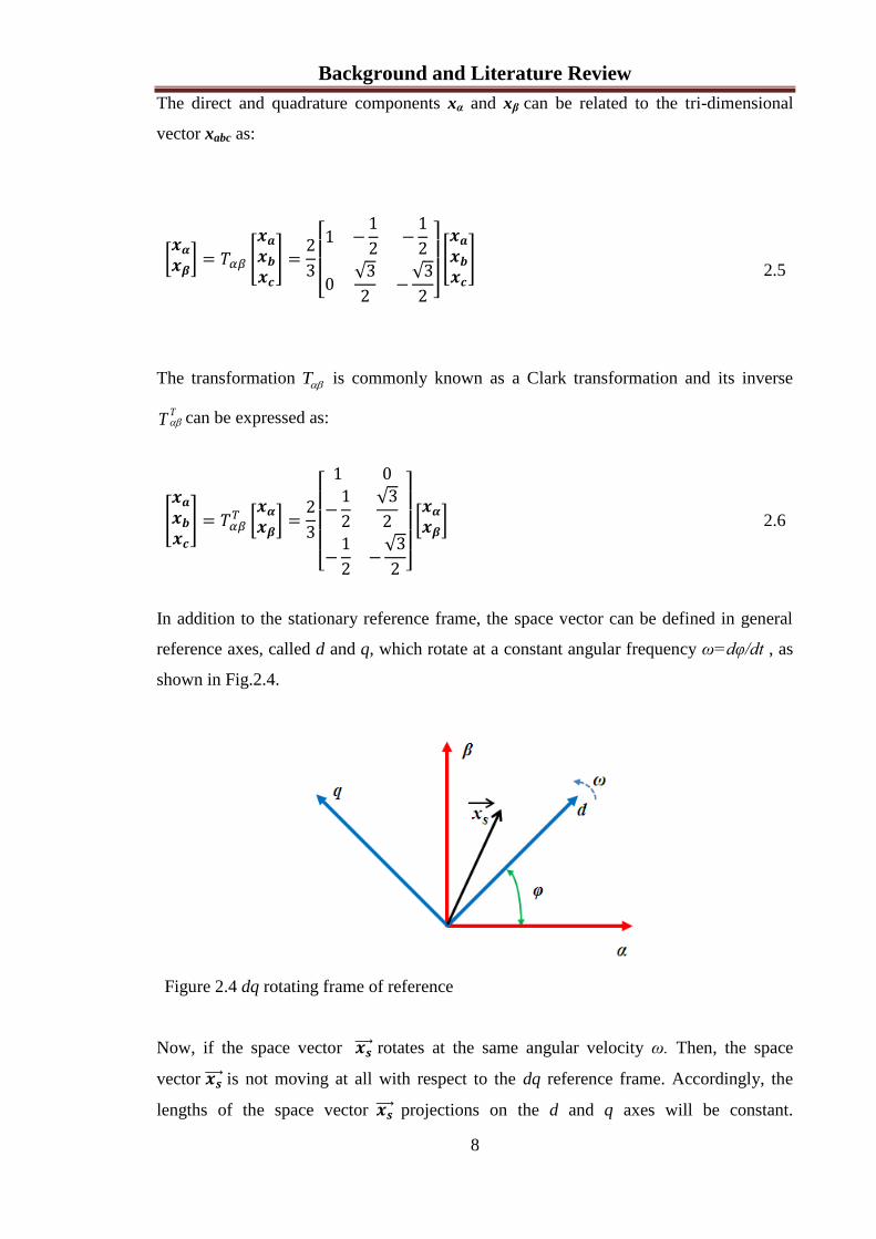
The direct and quadrature components xα and xβ can be related to the tri-dimensional
vector xabc as:
2.5
The transformation T is commonly known as a Clark transformation and its inverse
TT can be expressed as:
2.6
In addition to the stationary reference frame, the space vector can be defined in general
reference axes, called d and q, which rotate at a constant angular frequency ω=dφ/dt , as
shown in Fig.2.4.
Figure 2.4 dq rotating frame of reference
Now, if the space vector rotates at the same angular velocity ω. Then, the space
vector is not moving at all with respect to the dq reference frame. Accordingly, the
lengths of the space vector projections on the d and q axes will be constant.

Background and Literature Review
9
Considering Fig.2.4, it is possible to demonstrate that the d and q components of the
space vector are:
2.7
The transformation T dq is known as a Park transformation and its inverse TTdq can be
expressed as:
2.8
Furthermore, using complex representation, the space vector can be expressed as [20]:
2.9
2.4 Pulse Width Modulation Strategies
Pulse width modulation (PWM) is a powerful technique. It utilizes a square wave with a
modulated duty cycle to achieve the target average output voltage. The modulator’s
function is to produce timing pulses swa, swb, swc for the transistors from the reference
signals vmA, vmB, vmC (see Fig. 2.5). When the timing pulses swi=1, the top transistor in
Fig.2.1 is in the ON state, and the bottom transistor is in the OFF state, and vice versa for
swi=0. With these three control signals, swa, swb, swc, there are eight possible states, two
of which, (1, 1, 1) and (0, 0, 0), will not produce an output voltage. These states are called
zero vector states, while the other six states are called active vector states [21]. All the
possible states and their corresponding output voltages are summarized in Table 2.1.
Different techniques have been proposed for determining the switch ON times for fixed
frequency modulation systems. The most familiar strategies are now summarised [22]:

Background and Literature Review
10
State
vector
V dc
van V dc
vbn V dc
vcn V dc
vab V dc
vbc V dc
vca
000 0 0 0 0 0 0
100 2/3 -1/3 -1/3 1 0 -1
110 1/3 1/3 -2/3 0 1 -1
010 -1/3 2/3 -1/3 -1 1 0
011 -2/3 1/3 1/3 -1 0 1
001 -1/3 -1/3 2/3 0 -1 1
101 1/3 -2/3 1/3 1 -1 0
111 0 0 0 0 0 0
Table 2.1 The eight possible states and their output voltages
A. Naturally sampled PWM
In this approach the target reference waveform is compared with a high frequency carrier
signal to produce the PWM signal. The switch ON time is determined from the
instantaneous real-time intersection of these two signals. It is difficult to obtain these
intersections since this requires a transcendental equation to be solved when digital
implementation is adopted. However, it is easy to implement with analogue system. This
strategy is illustrated in Fig.2.5 where it is employed in sinusoidal pulse width
modulation.

Background and Literature Review
11
Figure 2.5 Sinusoidal pulse-width modulation (SPWM)
B. Regular sampled PWM
Regular sampled PWM is used to overcome the above-mentioned difficulties relating to a
naturally sampled scheme. The low frequency reference signal is sampled and held
constant during each carrier interval. Comparisons of these sampled values against the
high frequency carrier produce the switch ON time of each phase leg. Depending on the
sampling strategy, the sampled values are updated at either the positive, or positive and
negative peaks, of the carrier waveform.
The regular sampled PWM is classified into symmetrical and asymmetrical sampling.
With symmetrical sampling, the low frequency reference signal is sampled at the peak of
the triangular carrier. When the sampling occurs either in the positive or negative peaks
of the triangular carrier, i.e. the reference is re-sampled every half carrier period, this
strategy is called asymmetric sampling. There is no symmetrical and asymmetrical
concept when a saw tooth carrier is used because the reference signal is sampled at the
end of the ramping period.

Background and Literature Review
12
There are many modulation strategies; the most common are fixed frequency strategies
such as sinusoidal pulse width modulation (SPWM), space vector pulse width modulation
(SVPWM), and the discontinuous pulse width modulation (DPWM). The following
sections discuss these strategies briefly.
2.4.1 Sinusoidal pulse width modulation
The principle of naturally sampled sinusoidal PWM is explained with the aid of Fig. 2.5,
where the three-phase sinusoidal reference signals vmA, vmB, and vmC are compared with
the triangular carrier vcr. The comparison determines the logic signals swa, and swb which
turn on and off the associated transistors. The resultant terminal voltages vAO and vBO are
equal to the positive half of the DC link voltage when the related logic signal is one.
Otherwise, these voltages are switched to the negative half of the DC link voltage for
zero logic signals. The line voltage vAB can be determined by vAB=vAO-vBO, with a
fundamental component denoted by vAB1.
In this strategy, the terms modulation index M and the normalised frequency ratio mf are
defined as:
cr
m
V
VM 2.10
o
cf
f
fm 2.11
Where m and cr are the peak values of the modulating and carrier waves respectively.
On the other hand, fo is the modulating signal frequency and fc is the carrier signal
frequency. The fundamental voltage magnitude and frequency are controlled by the
modulation index and the reference signal frequency, respectively.
The nth
harmonic solution for the phase leg and line to line voltage such as those of
Fig.2.5 are given by the following expressions [23]:

Background and Literature Review
13
tntm
nmMmJ
m n m
V
tMVV
tv
oc
ndc
ocddc
AO
cos
2sin
21
12
cos22
2.12
23cos
3sin
2sin
21
14
6cos
23
tntm
nnmMmJ
m n m
V
tMV
tv
oc
ndc
odc
AB
2.13
In (2.12) and (2.13), the term Jn represents the Bessel function of order n, ωo is the
fundamental frequency of the modulating and output waveforms, ωc is the carrier
frequency, m is the carrier index variable, and n is the baseband index variable.
It is clear from the equation that the maximum magnitude of fundamental line voltage for
this strategy is √3Vdc/2 when M=1, i.e. the maximum magnitude of the phase voltage is
Vdc/2. If the modulation index M is greater than unity, the fundamental voltage vAB1 is
boosted from 0.612Vdc at M=1 to 0.744Vdc at M=2 [24]. However, low-order harmonics
will be generated. Accordingly, this mode of operation, which is called over-modulation,
is rarely used due to either torque pulsation in drive application or slow dynamic response
in grid connected converter applications, where a low cut-off frequency low pass filter
become necessary. Furthermore, the output voltage will no longer linearly vary with the
modulation index.
It is worth mentioning that sinusoidal pulse width modulation can be implemented using
a regular sampled PWM scheme, as the reference modulating signal is either sampled
symmetrically or asymmetrically. The analysis of the two alternatives shows that
asymmetrical sampling is superior to the symmetrical due to suppression of the phase leg
harmonics when (m ± n) is even [23]. However, there is no significant difference
between asymmetric sampled PWM and natural sampled PWM when the normalised
frequency ratio is high.

Background and Literature Review
14
2.4.2 Space vector pulse width modulation
Space vector modulation (SVM) is one of the widely used techniques for modulating
voltage source inverters [25]. Assume ideal switches, the theory of SVM is based on the
fact that there are only eight possible switching states for a three-phase inverter, as listed
in Table 2.1 and shown in Fig.2.6.
Figure 2.6 Eight possible phase leg switch combinations for VSI
These possible combinations can be represented by two zero space vectors ( and )
and six active space vectors ( to ). For a balanced three-phase system, we have:
0 tvtvtv cnbnan 2.14
Where van, vbn, and vcn are the instantaneous load phase voltages. Using Clark
transformation, it is possible to transfer these voltages to equivalent two-phase voltages
as:

Background and Literature Review
15
tv
tv
tv
tv
tv
cn
bn
an
2
3
2
30
2
1
2
11
3
2
)(
2. 15
The coefficient (2/3) is a scaling factor that allows the magnitude of the two phase
voltages equal to that of three-phase voltages after transformation. These two phase
voltages can be represented as a space vector:
tjvtvtV
)( 2.16
Substituting (2. 15) in (2.16), yields:
e jtve jtve jtvtV cnbnan 34
320
3
2)(
2.17
Applying the above equation to the vector in Table 2.1 yields:
e jVV dc0
3
21
2.18
Similarly, all six active vectors can be obtained as:
e kkjVV dck6,.....,2,1,
31
3
2
2.19
These voltage vectors are equal in magnitude and divide the α-β complex plane into six
equal regions within a regular hexagon, as shown in Fig.2.7.
The objective of the space vector technique is to synthesise the reference voltage vector
by means of the nearest two non-zero active vectors and the zero active vectors to

Background and Literature Review
16
obtain optimal harmonic performance [26]. Assuming the sample time Ts is small enough,
the reference vector can be assumed to be constant during Ts. When the reference
voltage lies in the first sector I, it can be synthesised as in Fig.2.8 where the vectors ,
, and are used.
Figure 2.7 Possible space vectors.
Figure 2.8 Creation of the reference voltage vector in sector I.
The volt-second balancing equation is:

Background and Literature Review
17
2.20
Where T1, T2, and TO, are the required times for the application of vectors , , and
respectively. Applying, k =0, 1, 2, the space vectors in (2.19) can be expressed as:
0,33
2,
3
2, 21
odcdcrefref Ve jVVVVe jVV
2.21
Substituting (2.21) into (2.20) and then splitting the imaginary and real components
yields:
3sin
31
dc
refs
V
VTT
sin3
2
dc
refs
V
VTT
21 TTTT so
For
2.22
These equations can be expressed in terms of the modulation index M as:
3sin1 MTT s
21
2 sin
TTTT
MTT
so
s
2.23
Where:

Background and Literature Review
18
dc
ref
V
VM
3 2.24
It is clear that the maximum amplitude of the reference voltage is limited by the largest
circle within the hexagon. Accordingly, the Vref,max can be found as:
36cos
3
2max,
dcdcref
VVV
2.25
Therefore, the maximum modulation index for SVM will be unity and the maximum
magnitude of fundamental line voltage for this strategy is Vdc, while for the SPWM
strategy, the maximum magnitude of fundamental line voltage is √3 Vdc/2. This indicates
that the SVM strategy boosts the output voltage by 15.4%.
A specific switching sequence arrangement is required to construct in each sector.
To minimize the switching losses, the sequence should be achieved with the minimum
number of switching actions during transition from one state to the next and from one
sector to another. Figure 2.9 depicts two of the possible vector arrangements in sector I. It
is clear that the first sequence is superior to the second, since the total number of
switching actions during the sampling period is six and no switching is required during
the transition from one sector to the next. Therefore, the second arrangement is
undesirable since ten switching actions are involved during the sampling period.
Table 2.2 gives the seven-segment switching sequence in all six sectors when sequences
similar to that shown in Fig.2.9 (a) are adopted.
The process described above can be implemented with either a symmetrical or
asymmetrical regularly sampled modulation strategy [27]. The required computations
may be doubled if the later scheme is adopted. Nevertheless, better harmonic
performance is obtained by using an asymmetrical regularly sampled strategy because of
the intrinsic even baseband harmonic cancellation [23]. Once more, the asymmetrical
regular sampled SVM has less harmonic distortion than the asymmetrical regular sampled
SPWM [28].

Background and Literature Review
19
(a) (b)
Figure 2.9 Seven-segment switching sequence for reference voltage in sector I:
(a) Desirable (b) Undesirable
Sector number Sector number
I
II
III
IV
V
VI
Table 2.2 Switching sequences for different sectors
2.4.3 Discontinuous pulse width modulation
The above mentioned SVM, which is referred to as classical SVM, distributes the zero
voltage vector period (To) equally between the two zero vectors and . However,
redistribution may affect the performance of the PWM strategy, such as the harmonic
content and the switching losses [29]. By using a single zero voltage vector, the switching
losses can be reduced as fewer commutations are required. Additional harmonics may be
introduced with this scheme, which is called discontinuous PWM. An improved strategy
can be used and this is called 60˚ discontinuous modulation, where each phase leg carries
the maximum current is now un-modulated for 60˚ at a time. This means the phase leg
will clamp either to the positive or negative DC rail. When the non-switching periods for
Background and Literature Review
20
each phase leg are centred on the positive and negative peaks of the reference voltage,
this is called DPWM1. This is the best scheme for a resistive load since the line current is
in phase with the fundamental voltage. Accordingly, each phase leg does not switch for
120˚ and this noticeably minimises the switching losses.
For loads that do not have a unity power factor, there is freedom to relocate the clamped
periods that minimise the switching losses. For lagging power factor load, it is preferable
to delay the non-switching periods up to maximum of 30˚, and this scheme is referred to
as DPWM2. Similarly, the non switching periods can be advanced by up to 30˚ for a
leading power factor, known as the DPWM0 strategy.
Figure 2.10 shows the non-switching periods for the three-phase legs that are clamped to
the DC rails for the mentioned strategies. The switching sequence for these strategies in
the first sector is depicted in Fig.2.11, while those for the other sectors are summarised in
Table 2.3 [30].
It is worth mentioning that the DPWM strategies have the same linearity range as the
SVPWM, i.e. they have the same DC bus utilisation [31] [32]. Furthermore, Fig.2.11
indicates that the DPWM strategies have fewer switching losses compared to the
SVPWM and SPWM [33]. However, these losses are considerably influenced by the load
power factor and the selected DPWM strategy.
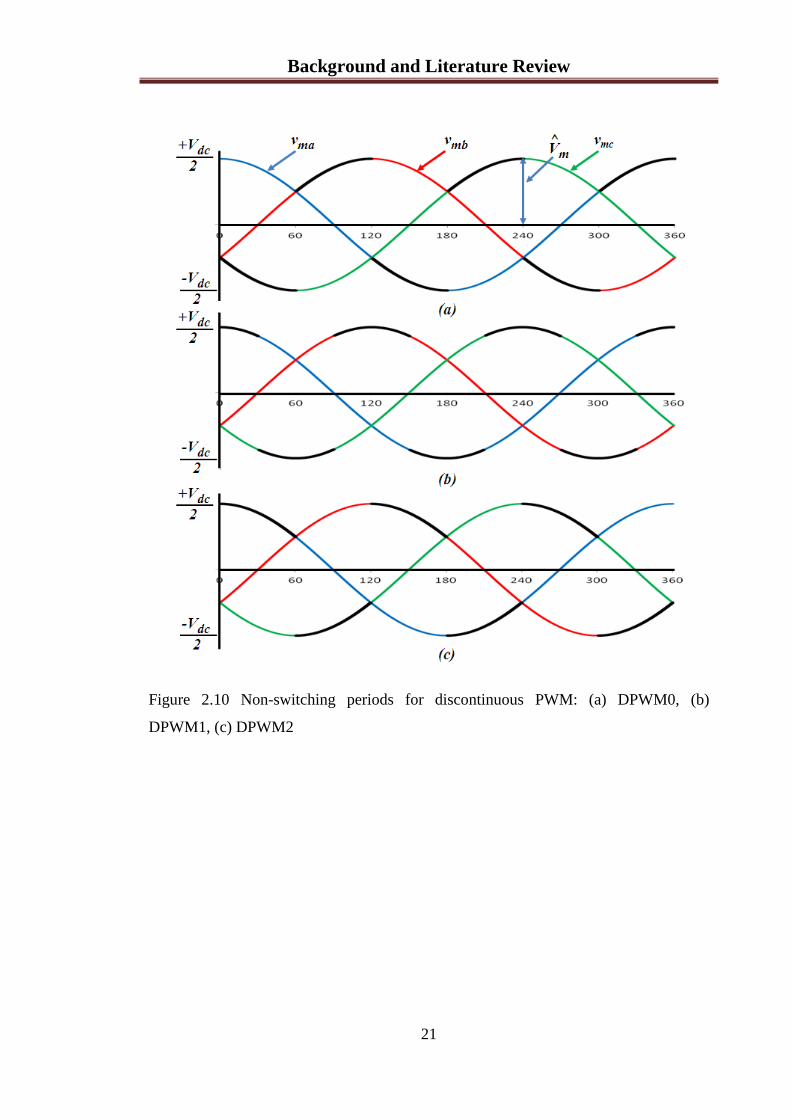
Background and Literature Review
21
Figure 2.10 Non-switching periods for discontinuous PWM: (a) DPWM0, (b)
DPWM1, (c) DPWM2
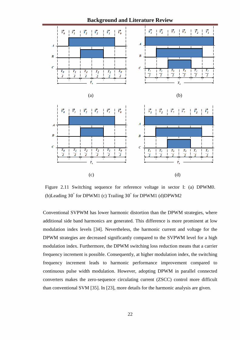
Background and Literature Review
22
(a) (b)
(c) (d)
Figure 2.11 Switching sequence for reference voltage in sector I: (a) DPWM0.
(b)Leading for DPWM1 (c) Trailing for DPWM1 (d)DPWM2
Conventional SVPWM has lower harmonic distortion than the DPWM strategies, where
additional side band harmonics are generated. This difference is more prominent at low
modulation index levels [34]. Nevertheless, the harmonic current and voltage for the
DPWM strategies are decreased significantly compared to the SVPWM level for a high
modulation index. Furthermore, the DPWM switching loss reduction means that a carrier
frequency increment is possible. Consequently, at higher modulation index, the switching
frequency increment leads to harmonic performance improvement compared to
continuous pulse width modulation. However, adopting DPWM in parallel connected
converters makes the zero-sequence circulating current (ZSCC) control more difficult
than conventional SVM [35]. In [23], more details for the harmonic analysis are given.

Background and Literature Review
23
Sector DPWM0 DPWM1 DPWM2
1
Leading
Trailing
2
Leading
Trailing
3
Leading
Trailing
4
Leading
Trailing
5
Leading
Trailing
6
Leading
Trailing
Table 2.3 DPWM switching sequences for different sectors
2.5 Current Control Techniques for a Three-Phase Voltage Source Inverter
Current control techniques can be divided into two major classes: linear and nonlinear
controllers [36]. Linear controllers for AC machine control include PI controllers either in
the stationary or synchronous reference frame, and constant frequency predictive control.

Background and Literature Review
24
The predictive controller is the more complex and requires knowledge of the load
parameters [37] [38]. Types of non-linear controller include hysteresis, delta modulation,
neural networks and fuzzy controllers.
The following sections will briefly describe the most popular current control for the
three-phase voltage source inverter, such as PI and hysteresis controllers.
2.5.1 Linear current controllers
Unlike non-linear current controller explained in section 2.5.2, linear controllers allow
the use of constant switching frequency modulation techniques such as SPWM and
SVPWM [36]. The basic reason for this is that linear controllers isolate the current error
compensation and PWM generation parts. The following methods will be explained when
SVPWM is adopted.
A- Stationary frame PI current controller:
Proportional-integral (PI) controllers can be used to generate the modulating signals for
the VSI. These modulating signals can be utilised by a carrier based modulator such as
SPWM or by SVPWM, as shown in Fig.2.12. The controller uses the αβ transformation
(Clark transformation) to operate on two variables instead of three when the abc
stationary frame is employed. This clearly simplifies the control algorithm and directly
generates the reference voltages for the SVM. The stationary frame PI regulator suffers
from significant steady state error since the PI controller provides finite gain at non-zero
frequency [37] [39]. However, employing a proportional resonance (PR) controller
instead of a PI controller results in a stationary frame current regulator with zero steady
state error [40] [41].
B-Synchronous frame PI dq current regulators
As mentioned in section (2.3), three-phase sinusoidal currents are transformed to DC
components when the dq synchronous frame is considered with an angular velocity (ω)
that is exactly equal to the three-phase system fundamental frequency [42].

Background and Literature Review
25
Figure 2.12 A stationary frame PI current regulator
Figure 2.13 depicts a synchronous frame PI dq current regulator. Two of the three motor
currents are measured and transformed to the dq synchronous frame with aid of the Clark
and Park transformation. The difference between the reference and measured dq frame
currents produces the target voltages in the dq frame. The dq frame target voltages are
transformed back to the stationary αβ frame to be utilised by the SVPWM block to
produce the required gate signals. In contrast to the stationary frame PI regulator, the dq
regulator can achieve zero steady state error by acting on DC signals. However, the
synchronous PI regulator is more complex since more transformations are required.
Furthermore, inaccurate synchronous frame identification may introduce noticeable error
in these transformations.
Figure 2.13 A synchronous frame PI dq current regulator
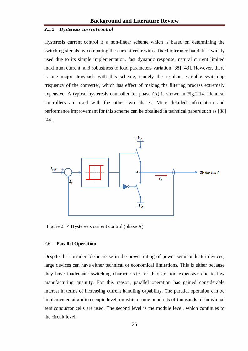
Background and Literature Review
26
2.5.2 Hysteresis current control
Hysteresis current control is a non-linear scheme which is based on determining the
switching signals by comparing the current error with a fixed tolerance band. It is widely
used due to its simple implementation, fast dynamic response, natural current limited
maximum current, and robustness to load parameters variation [38] [43]. However, there
is one major drawback with this scheme, namely the resultant variable switching
frequency of the converter, which has effect of making the filtering process extremely
expensive. A typical hysteresis controller for phase (A) is shown in Fig.2.14. Identical
controllers are used with the other two phases. More detailed information and
performance improvement for this scheme can be obtained in technical papers such as [38]
[44].
Figure 2.14 Hysteresis current control (phase A)
2.6 Parallel Operation
Despite the considerable increase in the power rating of power semiconductor devices,
large devices can have either technical or economical limitations. This is either because
they have inadequate switching characteristics or they are too expensive due to low
manufacturing quantity. For this reason, parallel operation has gained considerable
interest in terms of increasing current handling capability. The parallel operation can be
implemented at a microscopic level, on which some hundreds of thousands of individual
semiconductor cells are used. The second level is the module level, which continues to
the circuit level.
Background and Literature Review
27
Special care should be taken to ensure equal current sharing between the parallel
connected modules, such as IGBTs. Differences in the current level can occur in steady
state or dynamic operation. In steady state the device output characteristic which is the
collector current (IC) as a function to the collector to emitter voltage (VCE) affects the
current distribution. The major current is handled by the switch with lower on-state
voltage leading to higher conduction losses and junction temperature. The temperature
coefficient plays an important role in this situation. If the temperature coefficient is
positive, as in the MOSFET and most IGBT devices, even current sharing will occur
automatically. In contrast, negative temperate coefficient, as in freewheeling diodes, may
cause thermal overload in parallel connected devices. Furthermore, circuit parasitic
impedances affect the steady state current sharing. Parasitic resistances can be introduced
by the IGBT terminal connections for both the emitter and collector sides. For this reason,
the IGBT connections should be short and uniform.
It is also essential to investigate the current sharing during turn-on or turn-off periods.
The current distribution is highly affected by the IGBT transfer characteristic which is the
collector current as a function to the gate to emitter voltage (VGE). Under the same gate
conditions for parallel IGBTs, the device with steeper transfer characteristics handles a
larger current and then has the highest switching losses. Dynamic current sharing is more
sensitive to stray inductance in the gate emitter circuit. The stray inductance reduces the
effective gate voltage. Different emitter stray inductances will lead to non-simultaneous
switching and contribute to uneven switching losses.
Based on the points mentioned above, the following are the important precautions that
should be applied:
It is recommended that when driving parallel transistors, a common driver circuit
should be used to avoid differing signal propagation times. Also, an individual
gate resistor with each transistor should be used to eliminate risk of parasitic
oscillations [45]
All the power and drive circuits within the parallel switches should have a
minimum of stray inductance and strictly symmetrical wiring. As the number of
parallel devices is increased, this becomes more difficult to achieve [46]
Good thermal coupling between parallel modules should be ensured [1]
With optimum driver circuit implementation, thermal coupling, and layout
conditions, a de-rating factor of at least 10% is recommended [46]

Background and Literature Review
28
Based on the above discussion, paralleling IGBTs or MOSFETs is not always a good
option and the power stage may need a new design with each increment in the current
rating. Therefore, parallel operation at the converter level has received more interest,
especially for operation without galvanic isolation. This is mainly achieved through
software to reduce the necessary passive components size to limit the unbalanced current
distribution between the converters. Moreover, interleaving techniques can be adopted in
parallel converters operation. This technique has a significant impact on reducing the size
of the AC passive components [47].
2.7 Circulating Current and Cross Current: Definitions and Generation
The connection of power electronic converters in parallel can increase available power
levels, system reliability and efficiency and improve the flexibility of a system [9].
However, circulating currents are generated and this can lead to current waveform
distortion, unbalanced operation and a decline in overall system performance. Circulating
currents can flow between parallel connected converters unless they have uniform
modulation [16]. The reference waveforms and the carrier waveforms should therefore
have exactly the same amplitude, phase and frequency in order to prevent the flow of
circulating currents. The physical parameters of the system and the dead-time between
the upper and lower switching signals in each leg should also be closely matched, which
is not realistically possible. Recently, many studies have covered the circulating current
generation mechanism, its definition and modelling [9] [48] [49]. To illustrate the
circulating current generation mechanism two parallel connected AC/DC/AC converters
are considered, as shown in Fig.2.15.
To illustrate the forming of the circulating current and cross current paths, each transistor
and its anti-parallel diode will be represented by a single-pole single-throw switch.
Accordingly, the actual phase leg and its representation will be as shown in Fig.2.16. The
switch S1n is closed whenever the current flows through Q1n or the anti-parallel diode D1n.
As mentioned in section (2.4), there are eight possible switching states for each converter.
Therefore, there will be 64 possible switching state combinations for the two parallel-
connected converters. These states should be examined in order to find all the possible
current paths formed in the parallel connected system. Four of these will be considered as
options for exploring the possible current paths in such a system. The first is shown in
Fig.2.17 (a). The current paths are formed as follows:

Background and Literature Review
29
Figure 2.15 Directly paralleled AC/DC/AC converters.
Figure 2.16 Phase leg of an inverter: (a) Actual switching device (b) Single-pole single-
throw representation
Loop 1: P2-S12-La2-La1-S21-S41-Lb1-Lb2-S42-P2.
Loop2:P2-S12-La2-La1-S21-S61-Lc1-Lc2-S62-P2.
The current paths are formed through S41 and S61 (D41 and D61) since the DC link voltage
of the second units is applied to these diodes in the forward biased direction. A second
example is illustrated in Fig.2.17 (b).The resulting current loops are:
Loop1: P2-S32-Lb2-Lb1-S41-N1-S61-Lc1-Lc2-S62-P2.
Loop2: P2-S32-Lb2-Lb1-S41-N1-P1-S11-La1-La2-S12-P2.

Background and Literature Review
30
(a)
(b)
Figure 2.17 Cross current paths (a) Converter A in zero switching state and converter B
in active switching state (b)The two converters are in active switching states

Background and Literature Review
31
In loop 1, the current flow through S61 (because of the anti-parallel diode D61) is forward
biased by the DC link voltage of the second converter. Similarly, the diode D12 is forward
biased by the DC link voltage of the first converter. These current paths are normally
referred to as cross current paths, where the cross current can flow between the units by
forming closed paths through the other phases.
As the parallel converters are not completely identical, it can be seen that the circulating
current path still exists whether the two converters are synchronised or not. Figure 2.18
shows one of the possible circulating current paths when the two converters have the
same switching states. Such a circulating current is referred to as intrinsic circulating
current [50].
Considering the circuit in Fig.2.19 where different switching states are used by the
converters, it is clear that the two output inductors La1 and La2 are connected as an
inductive load to the rectifier. Therefore, a circulating current path is constructed though
the two converters. Furthermore, the switching states are the same as shown in Fig.2.17 (a)
i.e. both cross current and circulating current paths are formed in this specific case.
Similarly, a pure zero sequence circulating current path can be formed if the switching
state for the first inverter is (111) and the switching state for the second converter is
(000), or vice versa [20].
Figure 2.18 Intrinsic circulating current path when the two converters have the same
switching states

Background and Literature Review
32
Figure 2.19 Circulating current path when converter A in zero switching state and
converter B in active switching state
2.8 Interleaving Techniques
Interleaving techniques can be used to enhance the parallel-connected converters benefits
through reducing the equivalent output voltage ripple components [51]. To adopt
interleaved operation, all the parallel connected units should have the same switching
frequency and their carrier signals are phase shifted from each other, as shown in Fig.2.20.
The phase shift angle (λ) for N parallel connected units is 2 /N for symmetric
interleaving and between 0 and 2 /N for asymmetric interleaving.
Figure 2.20 Definition of interleaving angle (λ)
For analysis, consider two interleaved parallel connected VSCs, as shown in Fig.2.21,
which adopt naturally SPWM strategy. However, same analysis can be utilised for two
parallel- connected converters with separate but not isolated DC link (Fig. 2.15). Also,
similar analysis can be used with SVPWM or DPWM.

Background and Literature Review
33
Figure 2.21 Parallel connected VSCs
The nth harmonic solution for the switched phase-leg output voltage between the ac
terminal (e.g. A1) and the DC link mid-point is [23] [52]:
][][cos2
sin2
12
cos22
1
ooccn
m n
dc
odcdc
jkO
tntmnmMmJm
V
tMVV
tv
2.26
where θc and θo are the arbitrary phase offset angles for the carrier and fundamental
waveforms, respectively. The angle θo = 0,-2 /3, 2 /3 for phase legs A, B, and C
respectively and the angle θc = 0, λ for the first and the second converter, respectively.
When symmetrical interleaving is adopted, the nth harmonic solution for the phase leg
output voltage (phase A) is given as:
Background and Literature Review
34
][][cos2
sin2
12
cos22
1
1
tntmnmMmJm
V
tMVV
tv
ocn
m n
dc
odcdc
OA
2.27
][][cos2
sin2
12
cos22
1
2
tntmnmMmJm
V
tMVV
tv
ocn
m n
dc
odcdc
OA
2.28
It can be seen that all the harmonic voltages of the two converters are equal in magnitude
but different in phase. These harmonic voltages can be classified as:
1) Common mode (CM) harmonic voltages corresponding to the even mth-order and
odd triplen nth-order harmonics. These CM harmonics are in still in phase when λ
= . Accordingly, these harmonics will not contribute any output or circulating
current for the parallel system
2) CM harmonic voltages corresponding to the odd mth-order and even triplen nth-
order harmonics. However, although, these CM harmonic voltages are unable to
produce output currents, they can produce CM circulating current since the
second converter components are 180˚ apart from that of the first converter
3) Differential mode (DM) harmonic voltages corresponding to the even mth-order
and odd non-triplen nth-order harmonics. These voltages are not affected by
interleaving and produce an output current
4) Differential mode (DM) harmonic voltages corresponding to the odd mth-order
and even non-triplen nth-order harmonics. Due to interleaving, the harmonic
components of the second converter will be 180˚ out of phase with respect to the
first converter. Accordingly, the current produced by this group will not appear in
the total output current but will be changed to DM circulating current.
Based on the analysis in the frequency domain, high frequency circulating currents flow
between the parallel connected converters. Therefore, additional passive components are
necessary to mitigate both CM and DM circulating currents. Furthermore, interleaving
means that the PWM switching pulses of the two VSCs are phase shifted. This phase shift
is equivalent to a displacement between the output voltage vectors of the two converters,
and implies that the output voltage vectors will be in different sectors for a short period of
time when SVPWM or DPWM strategy is adopted. Therefore, the possibility of using
Background and Literature Review
35
different zero vectors by the two converters will be increased, and as a result, a low
frequency common mode circulating current will be generated [2] [3] and active current
control becomes necessary to limit such a circulating current. Conversely, with
interleaving the output current harmonics are reduced through switching frequency
harmonic cancellation, which is universal and independent of the PWM strategy [53].
Consequently, the current ripple frequency will be doubled and this permits considerable
reduction in the passive component size or in switching losses when operating a low
switching frequency. Also, harmonic cancellation effects occur in the common mode
voltage and the DC link current since the same harmonic elimination process occurs in all
three-phases [54].
2.9 Review of Control Methods for Parallel Connected Three-Phase Converters
Circulating current is the main issue with parallel connected converters and much work
has been carried out to resolve this problem. In order to prevent circulating currents one
can use separate DC or AC power supplies [55] [56] [57] [58] or an isolated AC sides via
a transformer [59] [60] [61] [62] . These approaches lead to increased system size and
cost with reduced efficiency due to core and copper losses when transformer is employed.
An alternative approach, however, is to utilise inter-module current sharing reactors on
the output terminals of each converter in order to provide high impedance in the
circulating current loop [63] [64] [65] [66] [67]. In [67], three-phase inter-module
reactors are used with a minimum inductance value, enough to allow safe operation at
minimum size, cost and weight. Unfortunately, this option will not provide a solution to
the low frequency circulating current.
Recent improvements in digital signal processing (DSP) controllers and advanced pulse
width modulation (PWM) techniques have increased the possibility of direct connection
of the DC and AC sides with smaller passive components to reduce the circulating
current. One frequent approach is to consider the parallel converters as one converter [63],
for example controlling two parallel, three-phase converters as a single converter. In this
case, the parallel voltage source inverter has 19 different voltage vectors. Using this
approach, increasing the number of parallel units makes the modelling and design of such
a control system complicated.
Parallel connected three-phase PWM rectifiers are controlled using converter flux-based
control (CFC) [68]. In this approach, the switching state is decided by the instantaneous
error between the reference and estimated active and reactive power. To control the zero
Background and Literature Review
36
sequence circulating current, the three-phase current for the N-1 converters is measured,
and then the zero sequence currents are calculated. The zero voltage vectors are selected
in accordance with the zero sequence current polarity.
One method of controlling the ZSCC was proposed in [6] for a parallel connected three-
phase rectifier and later used for parallel grid connected inverters [69] and [13]. With this
method, SVPWM is adopted and the ZSCC is calculated from the three-phase currents,
and a PI controller is used to decide the interval time of the zero vectors (000) and (111),
such that the ZSCC will be zero. The same approach has also been used but with a sliding
mode controller instead of a PI controller in order to bring advantages such as greater
signal stability and good dynamic response [70]. With a sliding mode controller, the
ZSCC can be better regulated compared with the PI controller method. This approach is
effective in zero-sequence circulating current reduction. Nevertheless, the effectiveness
diminishes when the zero vectors become smaller and saturate [68] [71]. Also, this
approach is not applicable if a DPWM strategy is adopted.
In [72], it is stated that the SVPWM naturally excites the zero-sequence circulating
currents. Thus, sinusoidal pulse width modulation (SPWM) is the best strategy to use for
the control of parallel converters with a common DC link. Accordingly, [73] has adopted
the SPWM to control directly connected AC and DC side three-phase converters.
However, this approach sacrifices the SVPWM advantages.
A special type of space vector modulation (SVM) [2] has been used to split the zero state
time intervals into four equal intervals. These intervals are equally distributed equally
between the existing active vectors and their opposite vectors, leading to an SVM without
zero vectors and consequently eliminating the pure zero sequence circulating currents.
However, circulating current is still generated due to any mismatches between the parallel
converters. This technique of SVM increases the switching losses and current ripple, and
reduces the maximum modulation index. Accordingly, relatively large inter-module
reactors have been used to achieve acceptable current waveforms.
Some works propose common mode circulating current control methods when DPWM
strategy is adopted [35] [74]. A zero sequence circulating current controller for
discontinuous pulse width modulation (DPWM) parallel connected inverters has been
investigated. The slave inverters adopt the same angle and modulation index of the
master inverter. The zero sequence circulation current for each slave inverter is calculated
and the zero- sequence modulation signal of the slave units are decided accordingly. If
the zero sequence circulating current is positive and greater than a positive threshold, the

Background and Literature Review
37
slave inverter uses the null vector (000). Conversely, if the zero sequence circulating
current reduces to the negative threshold, the null vector (111) will be used.
To control the circulating current in parallel connected converters for a direct-drive
permanent magnet wind power system, an improved SVPWM strategy has been adopted
[75]. Each module employs an independent synchronous frame PI dq current regulator.
The current regulator output is transformed back into the stator coordinate frame and fed
to a conventional SVPWM which produces the desired three-phase modulating signals.
These modulating signals for (N-1) modules are modified by a normalised zero sequence
voltage which is produced by a zero-axis PI regulator. This zero-axis PI regulator is
employed to mitigate the zero-sequence circulating current.
An open loop compensation dual-modulator has also been proposed to mitigate the ZSCC
[76]. In this scheme, the zero sequence modulating waveform of the master converter is
adopted by all the slave converters leading to a considerable reduction in the ZSCC. In
other words, one can use SVPWM with the master converter while SPWM is used with
the slave units. Then, the sinusoidal modulating signal of the slave units is added to the
zero sequence modulation waveform which is generated from the master converter. This
scheme does not require any additional current detecting device; however, the master-
slave control scheme has low reliability and robustness against failure [77].
Coordinate control is proposed in controlling parallel connected three-phase boost
rectifiers [50]. This strategy makes use of calculations of the line current symmetrical
components for all converters. After that, the zero and negative-sequence components are
eliminated using simple PI controllers, while the positive sequence line current
components are controlled for even load sharing. Furthermore, the nth converter positive
sequence d-axis current is considered the reference for the other converters. The same
approach is used for parallel converters with different load sharing [78].This approach is
very effective at mitigating circulating current, but heavy computational capability is
required to implement such an approach.
To enhance the benefits of paralleling VSCs, interleaved PWM rectifiers are proposed [2]
[3] [52] [79] [80]. In [2], the effect of an interleaved DPWM strategy in parallel-
connected PWM rectifiers is investigated. Accordingly, the authors claim that DPWM
should not be used together with interleaving techniques due to the appearance of low
frequency common mode circulating currents. This low frequency CM circulating current
is caused by the simultaneous use of different zero vectors between the two converters.
Therefore, SVM without zero vectors is recommended at the expense of higher switching

Background and Literature Review
38
losses and current ripple. The switching losses can be significantly reduced when SVM
without zero vectors based on a bicarrier scheme is adopted [81] [82]. In a bicarrier
SVPWM scheme the reference vector is composed of two adjacent active vectors, and
another two opposite active vectors, instead of using zero vectors. Compared to
conventional SVM, about 67% of the circulating current can be reduced when a bicarrier
SVM is employed in symmetrically interleaved converters. Conversely, the adoption of
multicarrier schemes increases system complexity. In [3], the interleaving angle should
be optimised in accordance with the modulation index and PWM strategy for the smallest
possible AC line inductor and EMI filter. Furthermore, a coupled inter-phase reactor
could be employed between the two PWM rectifiers to limit the circulating current
produced by interleaving. The size and weight of the coupled-inter-phase inductor can be
very small comparable to separate inductors which are commonly used as inter-phase
reactors. Unfortunately, the coupled inductor fails to provide low frequency CM
circulating current limitation. Also, with coupled inductors, each VSC cannot work only
by itself. For that reason, a three-phase common mode inductor is employed in the output
of each VSC instead of a coupled inter-phase inductor [12] [83]. Accordingly, the system
is more modular with the CM inductor, but the CM inductor can limit only the CM
circulating current, which is only apart from the total circulating current.
Neacsu [84] presents a comprehensive analysis which is required in the selection of a
PWM strategy to control interleaved three-phase converters. It is concluded that the
SPWM is more advantageous than the DPWM, which shows a very large zero sequence
circulating current if no zero-sequence controller is used.
To prevent the appearance of a low frequency CM circulating current caused by
interleaving, an active control method is explored [52] [80]. In this method, an additional
six switching actions per line cycle are added to the DPWM switching pattern to avoid
the simultaneous use of different zero vectors between the two converters. This control
method is enhanced with the coupled inter-phase inductors to control the high frequency
circulating current.
The research explored thus far has not proposed a simple algorithm which may need
critical intercommunication lines between modules or additional passive components that
could reduce the system reliability and expandability. Consequently, this thesis presents
new active current sharing control schemes. A simulation model, along with practical
implementation, will be used to validate the proposed method.

Proposed Methods
39
Chapter 3. Proposed Methods
This chapter explains the proposed current sharing control schemes for equally rated
synchronised parallel connected three-phase AC/DC/AC converters. The considered
system structure is shown in Fig.3.1, where the two converters are directly paralleled with
separate but not isolated DC buses. In accordance with the practical implementation (see
chapter 5), the two converters are supplied from an oversized 5kVA delta/star transformer.
The oversized transformer provides a satisfactory input current smoothing and, for that
reason, input line inductors are not employed. Four active current sharing control
methods are analysed and discussed.
Figure 3.1 Directly paralleled AC/DC/AC converters
3.1 Time Sharing Approach
To achieve equal current sharing for the parallel connected AC/DC/AC converters, a time
sharing approach is proposed. For equally rated synchronised converters, the switching
cycle is divided evenly between the converters. In the first half of the switching cycle, the
first converter is supplied with conventional PWM gate signals, while the six IGBTs of
the second converter are supplied with a logic zero gate signals. This operation is
reversed for the second half of the switching cycle. Accordingly, most circulating current
paths no longer exist. This leads to inter-module reactor redundancy and size and weight

Proposed Methods
40
reduction as consequence. Also, the circulating current control becomes unnecessary and
each converter uses only its local information to obtain the desired current. Furthermore,
the rms value of the switching device current rating, the switching losses, and the heat
sink size are decreased. However, this scheme can only be adopted with a limited number
of parallel connected units since each converter has to handle the peak load current.
3.2 Average Current Sharing Control Scheme
The average current sharing scheme was first applied in parallel connected DC-DC
converters[85]. This scheme is also employed in parallel-connected single-phase inverters
and also in three-phase parallel-connected inverters [86] [87]. The average of the
instantaneous current value of all paralleled modules is calculated and compared with the
instantaneous current value of each unit. The error signal is utilised by the compensator to
modify the reference modulating index or the reference modulating signal to achieve
equal current sharing between the units. Therefore, when a three-phase parallel connected
converter system is employed, each phase requires a compensator to make the
instantaneous value track the average of the instantaneous current values of all the
paralleled modules.
Unlike the aforementioned work, this thesis considers the magnitude of the current space
vector, instead of the instantaneous current value for each phase. To investigate the ZSCC
reflection in the current space vector magnitude, assume that there is a common mode
current superimposed on the balanced three-phase converter current such that:
3.1
Where:
Then, the magnitude of the current space vector will be:
Proposed Methods
41
3.2
It is clear that the common mode current is reflected in the current space vector
magnitude. In the same way, the current space vector magnitude will reflect the negative
sequence current riding on the balanced three-phase converter current. Accordingly,
converter currents represented by the space vector magnitude can be used in the current
sharing control, instead of representing the currents in the stationary reference frame or
dq rotating reference frame. Therefore, each converter will employ only one PI
compensator to achieve equal current sharing between the converters. Also, only one
piece of information needs to be shared between the converters.
3.2.1 Current sharing regulation analysis
The parallel-connected converters with inter-module reactors supplying a three-phase
inductive load can be represented as shown in Fig.3.2. Assuming balanced converter
output voltages and current sharing reactors, the equivalent circuit can be simplified as
shown in Fig.3.3.│Vsj│, │Isj| and |Is| are the converter output voltage, current, and load
current space vector magnitudes respectively and |Vcs| is the common coupling point
voltage space vector magnitude. The current sharing reactors are represented by the
impedance Zj. The three-phase load is modelled as a constant current source since the
load inductance is several times higher than that of the current sharing reactor. The PWM
inverter is represented by a voltage source controlled by the modulation index with a
linear gain (Kb ), which is equal to (3/ )|Vis|, where |Vis| is the input voltage space vector
magnitude.
The dead time effect and the switching device voltage drop reduce the inverter output
voltage and such effects can be modelled as a bias voltage source (|Vej|) connected in
series to the inverter output [88]. As a result, the inverter block diagram can be presented
as shown in Fig.3.4.
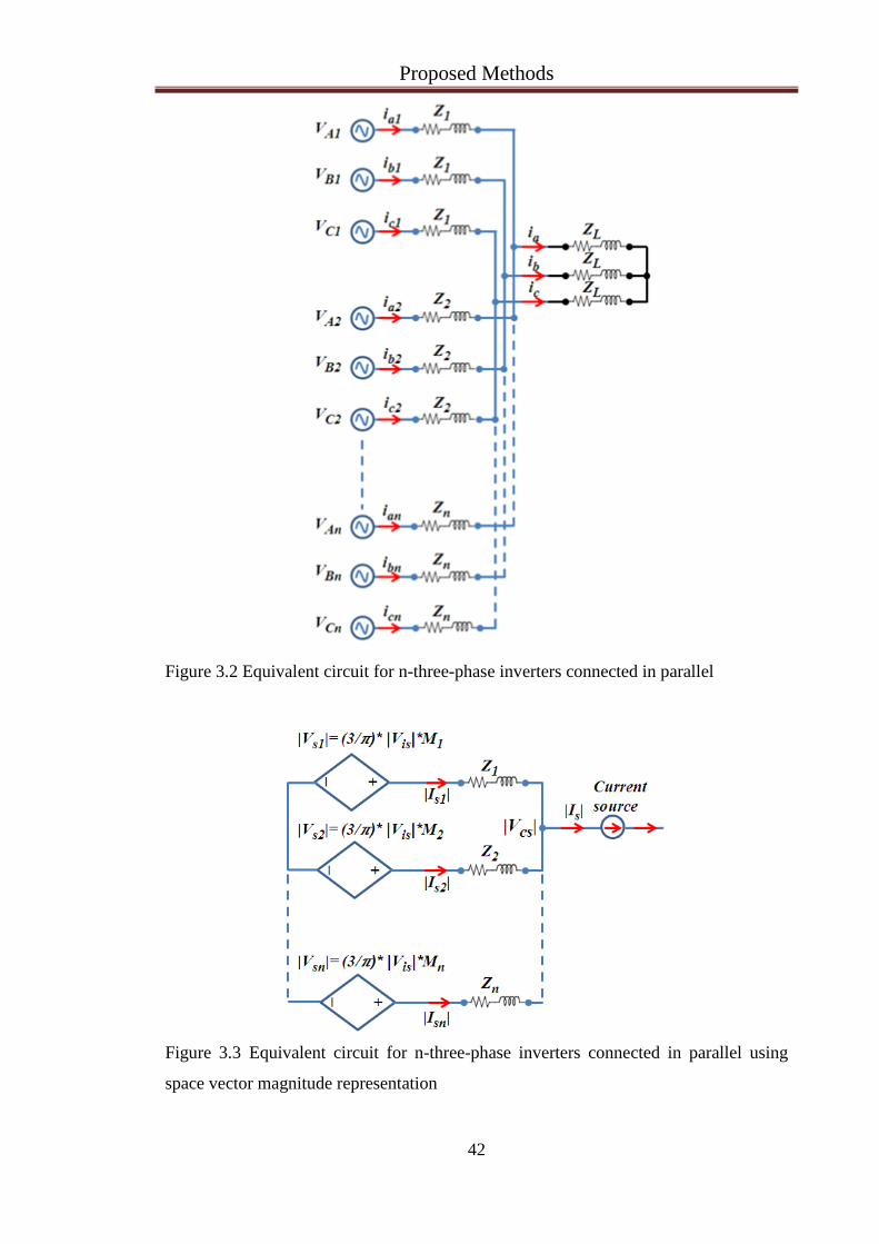
Proposed Methods
42
Figure 3.2 Equivalent circuit for n-three-phase inverters connected in parallel
Figure 3.3 Equivalent circuit for n-three-phase inverters connected in parallel using
space vector magnitude representation

Proposed Methods
43
Figure 3.4 Block diagram of three-phase inverter using space vector magnitude
representation
The current space vector magnitude for the jth
converter can be calculated as:
3.3
Where, Zj(s)=r+sL
Accordingly, the current space vector magnitude of each module in an n-parallel
connected system can be expressed as below:
3.4
The circulating current Icir-j(s) of the jth
module can be defined:

Proposed Methods
44
3.5
Where |Isav(s)| is the average of the current space vector magnitudes and can be expressed
as:
3.6
The average modulation index and the average bias voltage for the n modules can be
defined as:
3.7
Assuming small (less than 10%) current sharing reactors mismatch yields:
3.8
Thus, the average of current space vector magnitudes can be obtained as:
3.9
Using (3.4), (3.8) and (3.9) the circulating current of each module can be obtained as:
3.10
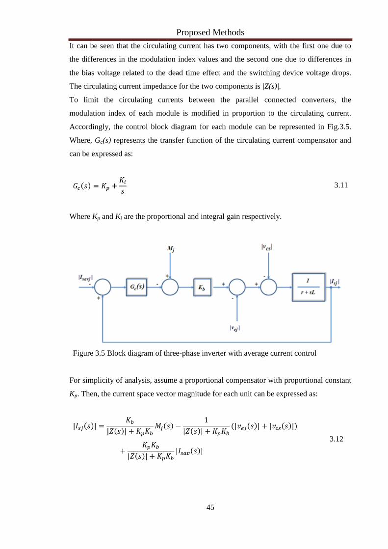
Proposed Methods
45
It can be seen that the circulating current has two components, with the first one due to
the differences in the modulation index values and the second one due to differences in
the bias voltage related to the dead time effect and the switching device voltage drops.
The circulating current impedance for the two components is |Z(s)|.
To limit the circulating currents between the parallel connected converters, the
modulation index of each module is modified in proportion to the circulating current.
Accordingly, the control block diagram for each module can be represented in Fig.3.5.
Where, Gc(s) represents the transfer function of the circulating current compensator and
can be expressed as:
3.11
Where Kp and Ki are the proportional and integral gain respectively.
Figure 3.5 Block diagram of three-phase inverter with average current control
For simplicity of analysis, assume a proportional compensator with proportional constant
Kp. Then, the current space vector magnitude for each unit can be expressed as:
3.12

Proposed Methods
46
Thus, using the set of (3.12) and (3.7), the average of current space vector magnitudes
can be defined as:
3.13
Substituting (3.12) and (3.13) in (3.5) yields:
3.14
It can be seen that the circulating current impedance for the two circulating current
components is increased. The circulating current impedance is equal to (|Z(s)|+KpKb )
instead of |Z(s)| when no current sharing control is adopted. For that reason, the
circulating current can be significantly reduced with suitable selection of proportional
compensator parameter. Furthermore, if the current sharing reactor impedance is much
smaller than KpKb, the parallel connected modules will have current distribution
independent of current sharing reactor mismatch (see (3.12)).
3.2.2 Design of PI controller gains
To obtain accurate discrete PI controller gain design of the sampled data system it is
necessary to determine an equivalent continuous time model that considers the delay time
(Td) produced by the sampling process and algorithm computation time [43]. The design
objective maximizes the controller gains (Kp & Ki) with a phase margin (ϕm) as the
forward path open loop gains tracks through unity [89]. Figure 3.6 represents the three-
phase inverter model with average current sharing control scheme. The sampling and
computation delay is modelled by an time delay block in the forward path.

Proposed Methods
47
Figure 3.6 Control diagram of three-phase inverter with delay effect
The sampling delay introduced in the system control loop is a quarter-carrier period since
asymmetrical regular sampled PWM is adopted with the average current sharing control
scheme [23]. On the other hand, the PWM duty cycle is updated each half-carrier period
because of the required algorithm computation time. This introduces an additional half-
carrier period delay time. With the aid of Fig.3.6, the open loop transfer function G(s) can
be expressed as:
3.15
The phase angle of G(s) at the cross over frequency ωc (i.e. the frequency at which unity
gain occurs at the desired phase margin ϕm) is given by:
∠
3.16
The term
can be approximated by
since
⟫ 1. Thus, from the last
equation:
3.17

Proposed Methods
48
This yields:
3.18
From (3.18), the maximum value of ωc can be obtained for a given ϕm is
3.19
By setting the open loop gain to unity at ωc(max), the maximum possible magnitude of Kp
can be calculated as below:
3.20
Equation (3.20) can be simplified to (3.21) since (ωc(max) Kp )⟫ Ki [43]and(ωc(max)L / r) ⟫
1 for typical AC current regulated system [89].
3.21
The integral gain can be obtained so that the mentioned assumption
/2 is
validated. This can be achieved using a suitable value to the integral gain as:
3.22

Proposed Methods
49
Using the system parameters L=1mH, r=0.05Ω, |Vis|=122.47V, Td=0.125msec, with a
suitable phase margin for satisfactory control performance of ϕm=40˚ [90] The controller
gains will be Kp=0.06 and Ki=4.2. The bode plot of the open loop transfer function is
presented in Fig.3.7 to verify the design where the phase margin and the cross over
frequency can be read. Different discretisation strategies like Euler (backward and
forward) and Trapezoidal can be used to achieve the digital equivalent of the PI analogue
controller gains. In both strategies, the digital and analogue proportional gains are equal,
while the digital integral gain can be obtained simply by multiplying the analogue
integral gain by the sampling period [43]. Further information on the transforms is
available in [91].
Figure 3.7 Magnitude and phase Bode plot of open loop forward path considering
delay effect Kp=0.06, Ki=4.2
3.3 Independent Current Sharing Control
An improvement to the previous method can be introduced through reduction in the
dependency of each converter control on the other converters. Unlike the previous
method, each converter will use only its local information to obtain equal current
distribution between the converters.

Proposed Methods
50
According to (3.2), the common mode circulating current will be reflected as a ripple in
the current space vector magnitude. The AC and DC components can be decomposed
using a low pass filter. The DC component is the fundamental positive sequence output,
and the AC component is the circulating current component. A PI compensator is used to
modify the reference modulation index, such that the current magnitude AC component
will track a zero reference value leaving only the DC component in the converter current
magnitudes. It can be seen that, with the control strategy shown in Fig.3.8, each converter
uses only one control loop without sharing information between the converters.
3.3.1 Current sharing regulation analysis
As mentioned in the previous sections, without current sharing control scheme, the
circulating current between the parallel connected converters can be expressed as:
3.23
To mitigate the circulating current, an independent current sharing control scheme is
proposed. Each inverter has the control block diagram shown in Fig.3.8.
Figure 3.8 Block diagram of three-phase inverter with independent current sharing
control
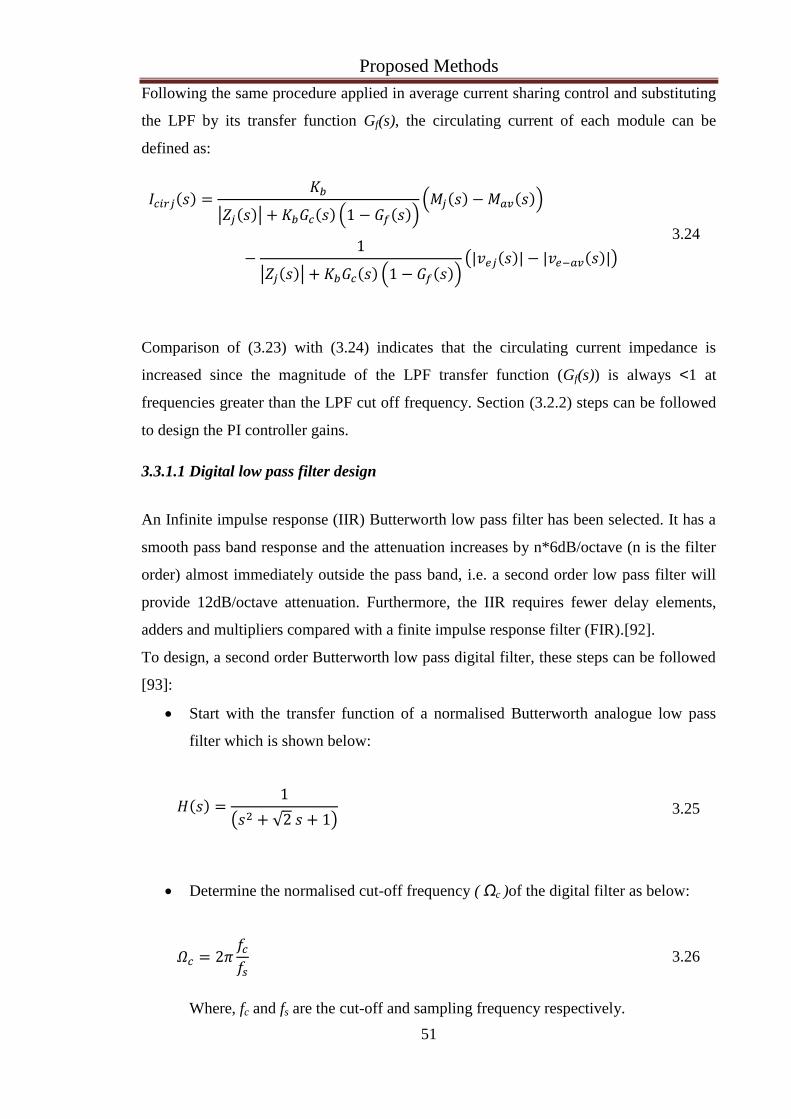
Proposed Methods
51
Following the same procedure applied in average current sharing control and substituting
the LPF by its transfer function Gf(s), the circulating current of each module can be
defined as:
3.24
Comparison of (3.23) with (3.24) indicates that the circulating current impedance is
increased since the magnitude of the LPF transfer function (Gf(s)) is always <1 at
frequencies greater than the LPF cut off frequency. Section (3.2.2) steps can be followed
to design the PI controller gains.
3.3.1.1 Digital low pass filter design
An Infinite impulse response (IIR) Butterworth low pass filter has been selected. It has a
smooth pass band response and the attenuation increases by n*6dB/octave (n is the filter
order) almost immediately outside the pass band, i.e. a second order low pass filter will
provide 12dB/octave attenuation. Furthermore, the IIR requires fewer delay elements,
adders and multipliers compared with a finite impulse response filter (FIR).[92].
To design, a second order Butterworth low pass digital filter, these steps can be followed
[93]:
Start with the transfer function of a normalised Butterworth analogue low pass
filter which is shown below:
3.25
Determine the normalised cut-off frequency ( Ωc )of the digital filter as below:
3.26
Where, fc and fs are the cut-off and sampling frequency respectively.
Proposed Methods
52
Determine the equivalent analogue filter cut-off frequency ωac, , using the pre-
warping function as of the following equation:
3.27
De-normalise the transfer function H(s) through replacing s with s/ωac
Use the bilinear transformation to transfer the analogue frequency response H(s)
to digital frequency response H(z). Where
3.28
Express the digital frequency response H (z) as a finite difference equation
Realise the difference equation with the SIMULINK blocks or with C language
code when the system is implemented with the DSP microcontroller.
These steps are followed to design a 50Hz, low pass filter with a 12kHz sampling
frequency. The achieved digital filter transfer function H(z) is:
3.29
Expressing the transfer function H(z) as a difference equation yields:
3.30
Finally, the LPF can be realised using the structure shown in Fig.3.9. Where
A0=0.0001682237, A1=0.0003364474, A2=0.0001682237, B1=1.96298, and B2=-
0.9636529. The frequency response of the designed filter is demonstrated in Fig.3.10.

Proposed Methods
53
Figure 3.9 Second order Butterworth LPF structure
Figure 3.10 Second order Butterworth LPF frequency response
3.4 Impedance Emulation Current Sharing Control Scheme
It is worth mentioning that increasing the current sharing reactor impedance reduces the
circulating current between the two converters at the cost of increased system size, cost
and losses [94] [95]. For these reasons, an active approach may be used to emulate
impedance increment. This is attained through modifying the magnitude of the converter
output voltage by an amount proportional to the converter current space vector magnitude,
as shown in Fig.3.11. Accordingly, the converter current space vector magnitude will be
as in (3.31). However, the current space vector magnitude for each module when no
current sharing control is employed is presented in (3.3), which is re-written as (3.32).
Comparison of the two equations ((3.31) and (3.32)), points out that the converter output

Proposed Methods
54
impedance magnitude is increased from |Zj| to (|Zj|+KZKb), where KZ is impedance
emulation factor. This will improve the current distribution between the parallel
connected converters. Therefore, this control technique can be considered as a virtual
impedance connected in series with the current sharing reactor.
3.31
3.32
Figure 3.11 Block diagram of three-phase inverter with impedance emulation current
sharing control
To select a suitable Kzvalue the simplified model shown in Fig.3.12 is used. The sampling
and computation delay is modelled by an time delay block in the forward path.
Figure 3.12 Three-phase voltage source converter model considering delay effect.

Proposed Methods
55
The delay block can be approximated as:
3.33
Accordingly, the closed loop transfer function between the converter current magnitude
and the reference modulation index can be defined as:
3.34
Using Routh’s stability criterion, the maximum allowable value for the emulation
impedance factor is [96]:
3.35
The delay time Td is equal to three quarters of the carrier period and one and half carrier
period for asymmetrical and symmetrical regular sampled PWM, respectively. Using the
mentioned system parameters Kb=(√6/ )*150, L=1mH, and Td=0.125msec, the
maximum allowable value for Kz is 0.138.
3.5 Summary
This chapter presented the proposed active current sharing control methods and their
current sharing analysis for the parallel-connected AC/DC/AC converters. In the time
sharing control scheme, the inter-module current sharing reactors are redundant, and only
local information was used by the converters. This is achieved through dividing the
operation time between the parallel-connected converters. The average current control
method can be adopted when current sharing reactors are employed at the output of each
converter. Current sharing analysis is presented through which the effect on the
circulating current impedance is explored. Also, the PI compensator which is employed

Proposed Methods
56
in this scheme is designed where the delay time produced by sampling process and
algorithm computation time is considered.
The independent current sharing control scheme is presented in a similar way to the
average current sharing control method. Unlike the average current sharing control
scheme, no information exchange between the two converters is needed leading to more
modular system. In the final approach the current distribution is improved through
impedance emulation, instead of increasing the physical impedance on the output of each
converter. The emulated impedance value is proportional to the converter current space
vector magnitude, i.e. a large emulated impedance is used when the converter shared
current is large and vice versa. The maximum allowable impedance emulation factor for
the parallel-connected converter is derived taking into account the delay time due to
sampling process and algorithm computation time. The control algorithm is simple and
modular since each converter is controlled independently of the other converters.
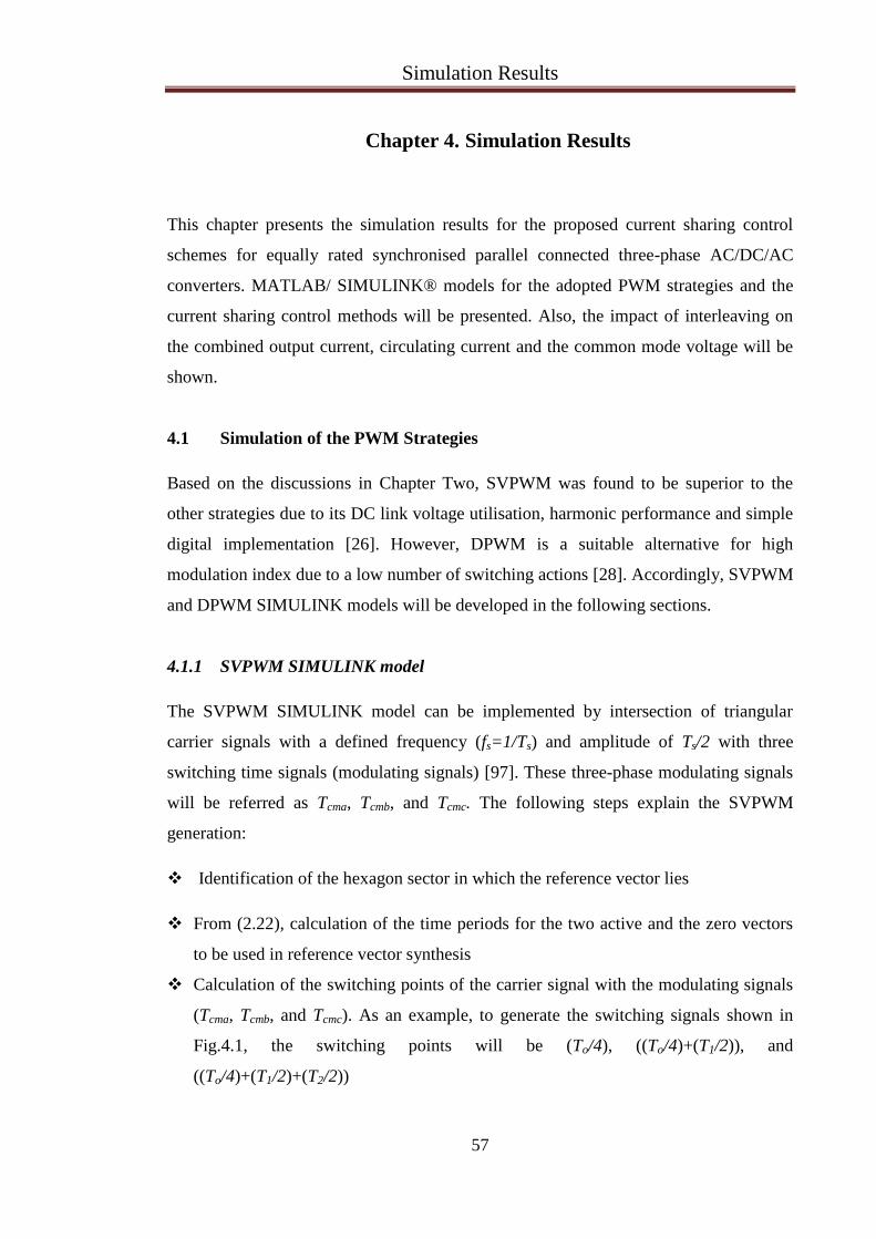
Simulation Results
57
Chapter 4. Simulation Results
This chapter presents the simulation results for the proposed current sharing control
schemes for equally rated synchronised parallel connected three-phase AC/DC/AC
converters. MATLAB/ SIMULINK® models for the adopted PWM strategies and the
current sharing control methods will be presented. Also, the impact of interleaving on
the combined output current, circulating current and the common mode voltage will be
shown.
4.1 Simulation of the PWM Strategies
Based on the discussions in Chapter Two, SVPWM was found to be superior to the
other strategies due to its DC link voltage utilisation, harmonic performance and simple
digital implementation [26]. However, DPWM is a suitable alternative for high
modulation index due to a low number of switching actions [28]. Accordingly, SVPWM
and DPWM SIMULINK models will be developed in the following sections.
4.1.1 SVPWM SIMULINK model
The SVPWM SIMULINK model can be implemented by intersection of triangular
carrier signals with a defined frequency (fs=1/Ts) and amplitude of Ts/2 with three
switching time signals (modulating signals) [97]. These three-phase modulating signals
will be referred as Tcma, Tcmb, and Tcmc. The following steps explain the SVPWM
generation:
Identification of the hexagon sector in which the reference vector lies
From (2.22), calculation of the time periods for the two active and the zero vectors
to be used in reference vector synthesis
Calculation of the switching points of the carrier signal with the modulating signals
(Tcma, Tcmb, and Tcmc). As an example, to generate the switching signals shown in
Fig.4.1, the switching points will be (To/4), ((To/4)+(T1/2)), and
((To/4)+(T1/2)+(T2/2))

Simulation Results
58
Generation by the switching point calculation of the required modulating waveforms
Tcma, Tcmb and Tcmc. Comparing these waveforms with the carrier signal produces the
switching signals for the three-phase inverter
Figure 4.1 Seven segments switching sequence for reference voltage in sector I
Table 4.1 summarises the intersection points of the modulating and carrier signals in
different sectors. The SIMULINK model realisation of SVPWM is shown in Figs.4.2 to
4.4. Figure 4.2 explains the modulating waveform generation where the active and zero
vector times are calculated and then Tcma, Tcmb, and Tcmc are calculated in accordance
with Table 4.1. Comparison of the modulating signals with the carrier signal will
produce the desired duty cycles for the inverter switches (see Fig.4.3). To avoid bridge
shoot through, it is recommended that a suitable dead time be added to the gate signals
of each inverter leg, as in the model shown in Fig.4.4. As a result of this dead time, the
first switch will be turned off, and then the other switch will be turned on after the dead
time period. For that reason, the dead time needs to be set to a time longer than the
switching off time of the inverter switches.

Simulation Results
59
Sector No. Tcma Tcmb Tcmc
I (To/4) (To/4)+ (T1/2) (To/4)+
(T1/2)+(T2/2)
II (To/4)+ (T2/2) (To/4) (To/4)+
(T1/2)+(T2/2)
III (To/4)+
(T1/2)+(T2/2) (To/4) (To/4)+ (T1/2)
IV (To/4)+
(T1/2)+(T2/2) (To/4)+ (T2/2) (To/4)
V (To/4)+ (T1/2) (To/4)+
(T1/2)+(T2/2) (To/4)
VI (To/4) (To/4)+
(T1/2)+(T2/2) (To/4)+ (T2/2)
Table 4.1 Switching points for modulating signals calculation
Figure 4.2 Modulating signals generator

Simulation Results
60
Figure 4.3 Seven segment SVPWM SIMULINK model
Figure 4.4 Dead time SIMULINK model
To assess the SVPWM SIMULINK model, a three-phase AC/DC/AC converter, shown
in Fig.4.5, is employed to supply a three-phase inductive load. Table 4.2 shows the
converter parameters and Figs.4.6 to 4.8 depict the simulation results. These figures
demonstrate the three-phase modulating signals, the three-phase load current and the
converter output voltage, respectively. It is obvious that three-phase load currents are
balanced with low total harmonic distortion.

Simulation Results
61
PWM strategy SVPWM
Input voltage 150V, 50Hz
Modulation index 0.866
Switching and sampling frequency 6kHz
Output line frequency 50Hz
Load 10Ω+18mH per phase
DC link capacitor 800µF
Dead time 2µsec
Table 4.2 AC/DC/AC converter parameters
Figure 4.5 SIMULINK model for three-phase AC/DC/AC converter

Simulation Results
62
Figure 4.6 Modulating signals for SVPWM strategy
Figure 4.7 Three-phase load current waveforms for SVPWM strategy

Simulation Results
63
Figure 4.8 Load line voltage based on SVPWM strategy
4.1.2 DPWM SIMULINK model
The same SVPWM SIMULINK model can be used to generate the gate signals when
DPWM is adopted. This can be achieved by calculating the new switching points for
modulating signals in accordance with the DPWM switching sequences mentioned in
Table 2.3. As an example, adopting the DPWM2 strategy produces the switching points
shown in Table 4.3.
Sector No. Tcma Tcmb Tcmc
I 0 (T1/2) (T1/2)+(T2/2)
II (To/2)+ (T2/2) (To/2) (Ts/2)
III (T1/2)+(T2/2) 0 (T1/2)
IV (Ts/2) (To/2)+ (T2/2) (To/2)
V (T1/2) (T1/2)+(T2/2) 0
VI (To/2) (Ts/2) (To/2)+ (T2/2)
Table 4.3 DPWM2 switching point calculations
The simulation results with the same converter parameters as those listed in. Table 4.2
are depicted in Figs 4.9 to 4.12. Figure 4.9 clarifies the 120˚ clamping periods in the
modulating signals, while Figs.4.10 and 4.11 shows the three-phase load voltage and
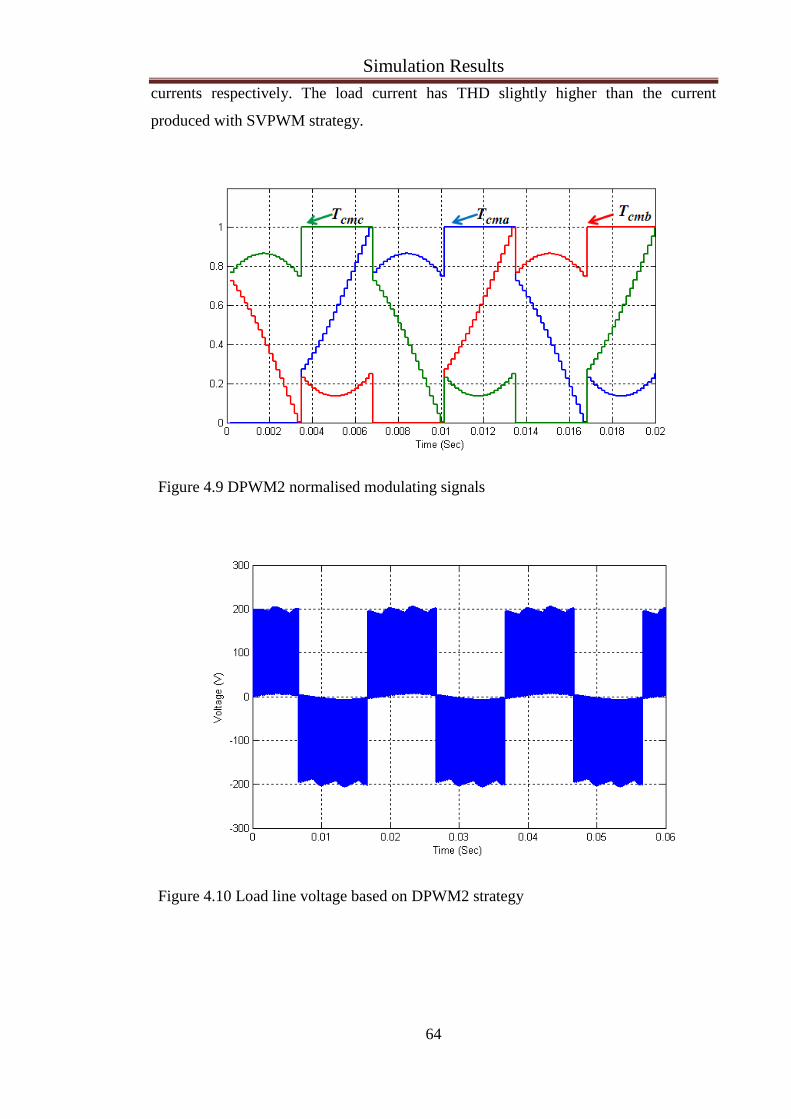
Simulation Results
64
currents respectively. The load current has THD slightly higher than the current
produced with SVPWM strategy.
Figure 4.9 DPWM2 normalised modulating signals
Figure 4.10 Load line voltage based on DPWM2 strategy
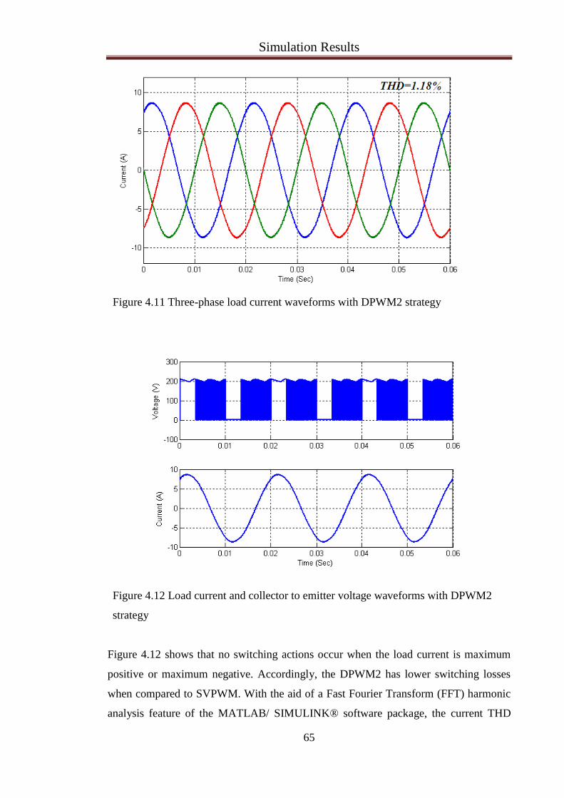
Simulation Results
65
Figure 4.11 Three-phase load current waveforms with DPWM2 strategy
Figure 4.12 Load current and collector to emitter voltage waveforms with DPWM2
strategy
Figure 4.12 shows that no switching actions occur when the load current is maximum
positive or maximum negative. Accordingly, the DPWM2 has lower switching losses
when compared to SVPWM. With the aid of a Fast Fourier Transform (FFT) harmonic
analysis feature of the MATLAB/ SIMULINK® software package, the current THD

Simulation Results
66
and current harmonics root-mean-square (rms) values (Ih, rms) have been calculated,
where:.
4.1
Where In,rms is the nth
harmonic current rms value. The calculations were conducted for
the AC/DC/AC converter with the parameters listed in Table 4.2 for both SVPWM and
DPWM2 strategies. The results are demonstrated in Figs.4.13.and 4.14
Figure 4.13 Current THD for SVPWM and DPWM2 strategies.

Simulation Results
67
Figure 4.14 RMS value of harmonic current components for SVPWM and DPWM2
strategies.
Figure 4.14 indicate that current harmonics rms values of the SVPWM are less than
DPWM2 especially at low modulation index values. However, the current harmonics
rms values for the DPWM2 strategy are decreased significantly to the SVPWM level for
a high modulation index. These results match well with the harmonic analysis given in
[98].
4.2 Time Sharing Approach
To verify the control proposed, a MATLAB/ SIMULINK® model for two parallel
connected AC/DC/AC converters is used (Fig.4.15). These converters have the
parameters listed in Table 4.4, where a 1µH inductor with 0.5mΩ is used to simulate the
cable impedance of the two converters.
In accordance with practical system implementation (chapter five), the two converters
are simulated as being controlled by one DSP microcontroller. The parallel converters
are used as a current controller for a three-phase R-L load. For simplicity, the converter
current is controlled through controlling the magnitude of the current space vector rather
than magnitude and phase. Consequently, each converter uses only one PI compensator
to attain the desired current magnitude. Figures 4.16 to 4.19 depict the different
SIMULINK model blocks for each subsystem.

Simulation Results
68
Parameter Value
Cable impedance 0.5mΩ+1µH
IGBT on resistance 1mΩ
IGBT forward voltage drop 1V
Freewheeling diode on resistance 1mΩ
Freewheeling diode voltage drop 0.7V
Rectifier diode on resistance 1mΩ
Rectifier diode forward voltage drop 0.8V
Switching and sampling frequency 6kHz
Desired output frequency 50Hz
Input voltage 3-φ, 150V, 50Hz
Dead time 2µsec.
Three-phase load 10mH+10Ω per phase
DC link capacitor 800µF
PWM strategy SVPWM
Table 4.4 Converters parameters with time sharing scheme
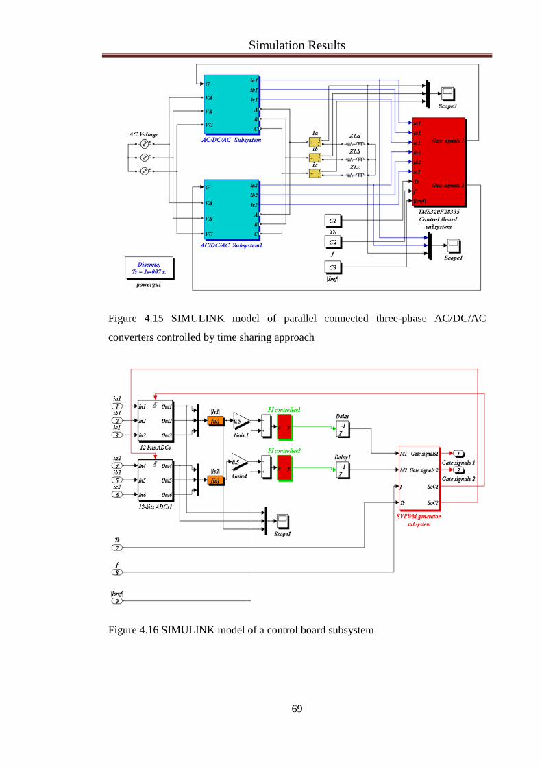
Simulation Results
69
Figure 4.15 SIMULINK model of parallel connected three-phase AC/DC/AC
converters controlled by time sharing approach
Figure 4.16 SIMULINK model of a control board subsystem

Simulation Results
70
Figure 4.17 ADC SIMULINK model
Figure 4.18 Discrete PI compensator SIMULINK model
Figure 4.19 SIMULINK of SVPWM generator subsystem
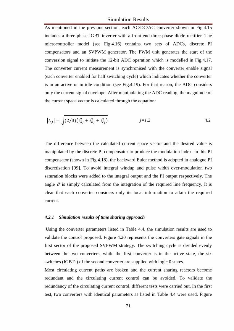
Simulation Results
71
As mentioned in the previous section, each AC/DC/AC converter shown in Fig.4.15
includes a three-phase IGBT inverter with a front end three-phase diode rectifier. The
microcontroller model (see Fig.4.16) contains two sets of ADCs, discrete PI
compensators and an SVPWM generator. The PWM unit generates the start of the
conversion signal to initiate the 12-bit ADC operation which is modelled in Fig.4.17.
The converter current measurement is synchronised with the converter enable signal
(each converter enabled for half switching cycle) which indicates whether the converter
is in an active or in idle condition (see Fig.4.19). For that reason, the ADC considers
only the current signal envelope. After manipulating the ADC reading, the magnitude of
the current space vector is calculated through the equation:
j=1,2 4.2
The difference between the calculated current space vector and the desired value is
manipulated by the discrete PI compensator to produce the modulation index. In this PI
compensator (shown in Fig.4.18), the backward Euler method is adopted in analogue PI
discretisation [99]. To avoid integral windup and pulse width over-modulation two
saturation blocks were added to the integral output and the PI output respectively. The
angle ϑ is simply calculated from the integration of the required line frequency. It is
clear that each converter considers only its local information to attain the required
current.
4.2.1 Simulation results of time sharing approach
Using the converter parameters listed in Table 4.4, the simulation results are used to
validate the control proposed. Figure 4.20 represents the converters gate signals in the
first sector of the proposed SVPWM strategy. The switching cycle is divided evenly
between the two converters, while the first converter is in the active state, the six
switches (IGBTs) of the second converter are supplied with logic 0 states.
Most circulating current paths are broken and the current sharing reactors become
redundant and the circulating current control can be avoided. To validate the
redundancy of the circulating current control, different tests were carried out. In the first
test, two converters with identical parameters as listed in Table 4.4 were used. Figure

Simulation Results
72
4.21 shows the load currents during the steady state and transient state due to a step
change in the desired current at t=0.05μsec. The three-phase output currents are almost
balanced with a THD equal to 1.49%. Also, the two converters share the current equally
during transient (step change in current from 3A to 4.5A) and steady state since
identical converter parameters are used. Figure 4.22 displays the two converter currents
for phase a, whilst Fig.4.23 shows the transient response for the converter’s output
current magnitude. The response is fast with minimum overshoot and zero steady state
error since the PI compensators deal with DC values. The output line voltage and its
fundamental component are monitored in Fig.4.24.
Figure 4.20 IGBTs gate signals when time sharing is adopted

Simulation Results
73
Figure 4.21 Three-phase load current during transient and steady states
Figure 4.22 Converter current with identical parameters using time sharing approach

Simulation Results
74
Figure 4.23 Converter current space vector magnitude for identical parameters using
time sharing approach
Figure 4.24 Load voltage and its fundamental component using time sharing approach
In the second test, two converters with different parameters were used. The first
converter parameters (switch on resistance, forward voltage drop, cable impedance, and
dead time) have the same parameters as those listed in Table 4.4, while the second
converter parameters are reduced by 30% from the values of the first converter. Figure
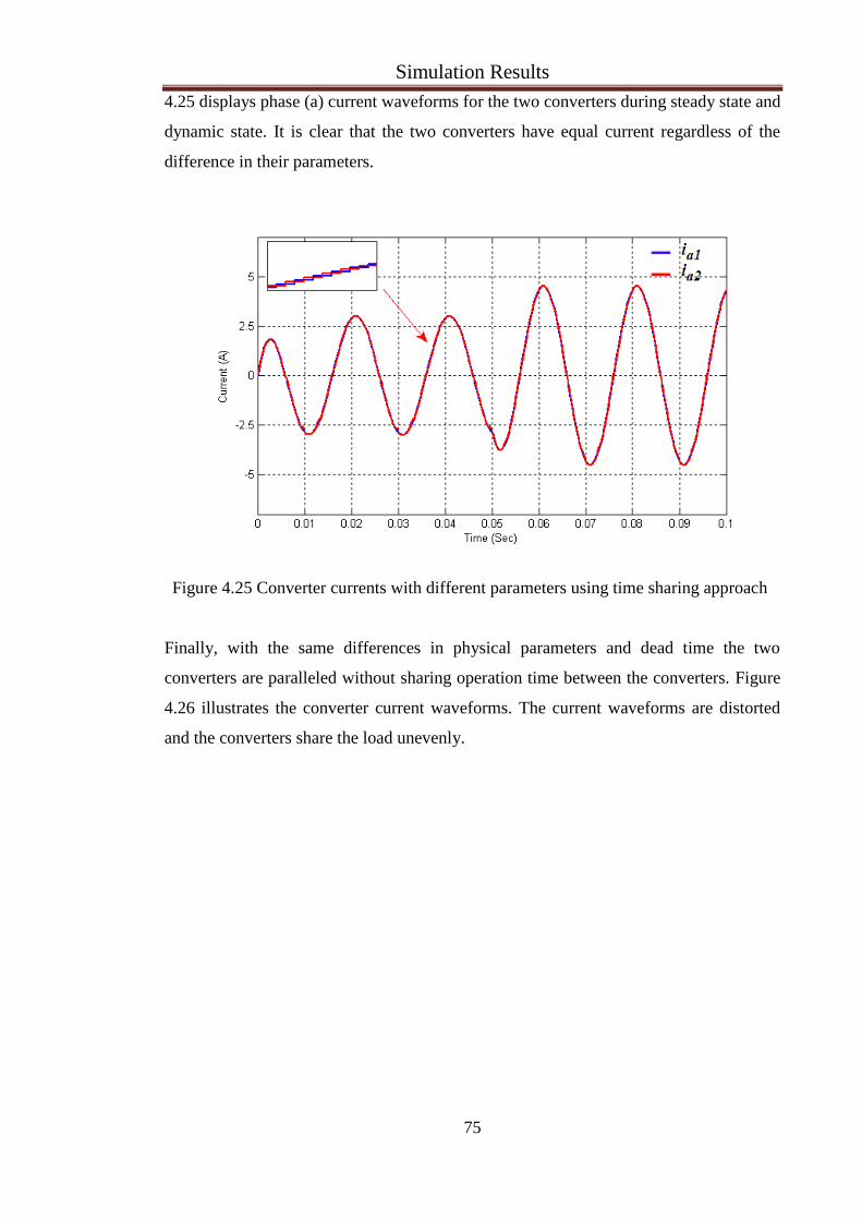
Simulation Results
75
4.25 displays phase (a) current waveforms for the two converters during steady state and
dynamic state. It is clear that the two converters have equal current regardless of the
difference in their parameters.
Figure 4.25 Converter currents with different parameters using time sharing approach
Finally, with the same differences in physical parameters and dead time the two
converters are paralleled without sharing operation time between the converters. Figure
4.26 illustrates the converter current waveforms. The current waveforms are distorted
and the converters share the load unevenly.
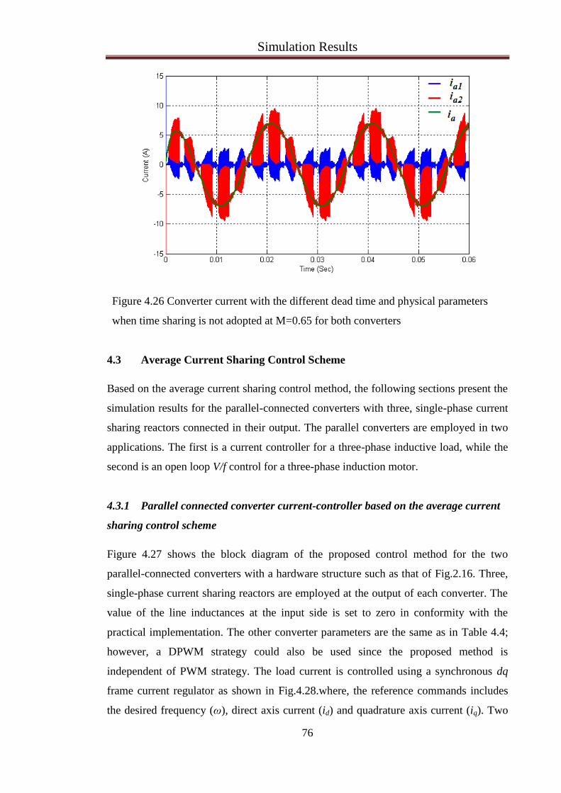
Simulation Results
76
Figure 4.26 Converter current with the different dead time and physical parameters
when time sharing is not adopted at M=0.65 for both converters
4.3 Average Current Sharing Control Scheme
Based on the average current sharing control method, the following sections present the
simulation results for the parallel-connected converters with three, single-phase current
sharing reactors connected in their output. The parallel converters are employed in two
applications. The first is a current controller for a three-phase inductive load, while the
second is an open loop V/f control for a three-phase induction motor.
4.3.1 Parallel connected converter current-controller based on the average current
sharing control scheme
Figure 4.27 shows the block diagram of the proposed control method for the two
parallel-connected converters with a hardware structure such as that of Fig.2.16. Three,
single-phase current sharing reactors are employed at the output of each converter. The
value of the line inductances at the input side is set to zero in conformity with the
practical implementation. The other converter parameters are the same as in Table 4.4;
however, a DPWM strategy could also be used since the proposed method is
independent of PWM strategy. The load current is controlled using a synchronous dq
frame current regulator as shown in Fig.4.28.where, the reference commands includes
the desired frequency (ω), direct axis current (id) and quadrature axis current (iq). Two

Simulation Results
77
PI controllers are employed to separately control id and iq. The PI controller outputs are
transformed back to the stationary αβ frame, and then a polar representation is used to
produce the desired base modulation index (Mbase) and angle ϑ. The converters’ current
space vector magnitude and the average of the current space vector magnitudes are
calculated using the following:
4.3
4.4
The difference between the converter current space vector magnitude and the average of
the current space vector magnitudes is calculated. This error is used by the PI
compensator to produce a suitable deviation in the base modulation index to attain equal
current sharing between the two converters.
Figure 4.27 Block diagram of parallel connected AC/DC/AC converter current
controller based on average current sharing control
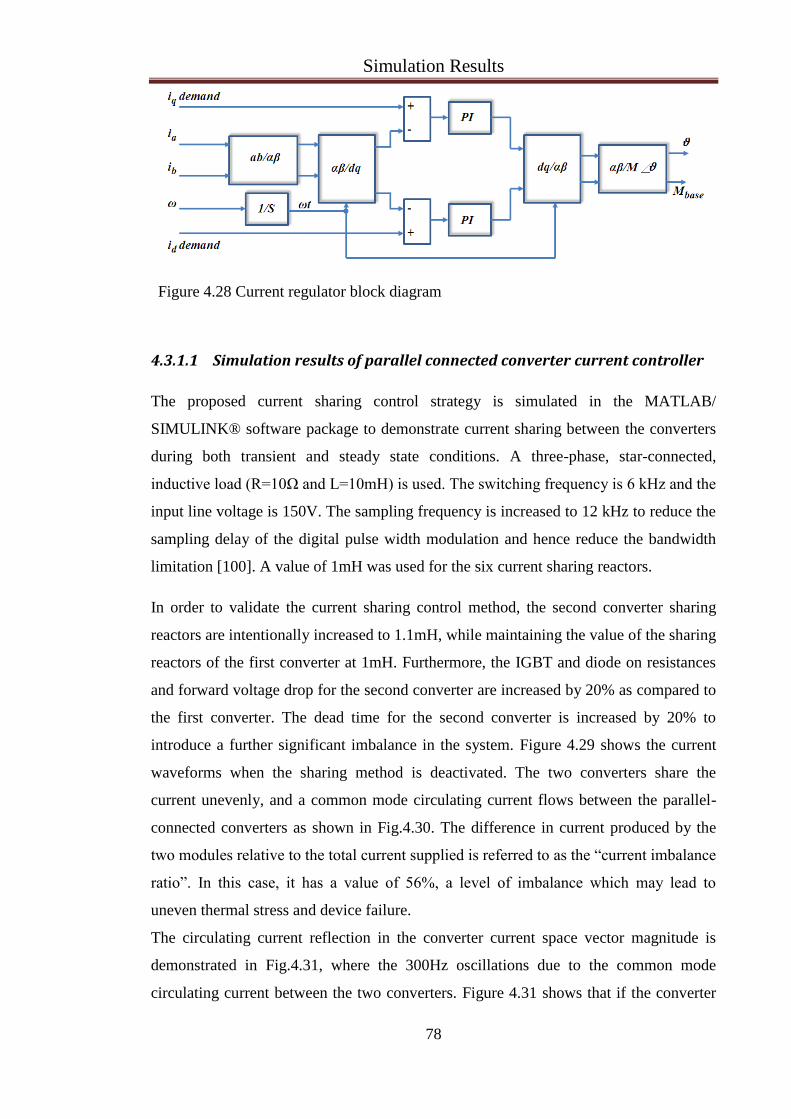
Simulation Results
78
Figure 4.28 Current regulator block diagram
4.3.1.1 Simulation results of parallel connected converter current controller
The proposed current sharing control strategy is simulated in the MATLAB/
SIMULINK® software package to demonstrate current sharing between the converters
during both transient and steady state conditions. A three-phase, star-connected,
inductive load (R=10Ω and L=10mH) is used. The switching frequency is 6 kHz and the
input line voltage is 150V. The sampling frequency is increased to 12 kHz to reduce the
sampling delay of the digital pulse width modulation and hence reduce the bandwidth
limitation [100]. A value of 1mH was used for the six current sharing reactors.
In order to validate the current sharing control method, the second converter sharing
reactors are intentionally increased to 1.1mH, while maintaining the value of the sharing
reactors of the first converter at 1mH. Furthermore, the IGBT and diode on resistances
and forward voltage drop for the second converter are increased by 20% as compared to
the first converter. The dead time for the second converter is increased by 20% to
introduce a further significant imbalance in the system. Figure 4.29 shows the current
waveforms when the sharing method is deactivated. The two converters share the
current unevenly, and a common mode circulating current flows between the parallel-
connected converters as shown in Fig.4.30. The difference in current produced by the
two modules relative to the total current supplied is referred to as the “current imbalance
ratio”. In this case, it has a value of 56%, a level of imbalance which may lead to
uneven thermal stress and device failure.
The circulating current reflection in the converter current space vector magnitude is
demonstrated in Fig.4.31, where the 300Hz oscillations due to the common mode
circulating current between the two converters. Figure 4.31 shows that if the converter
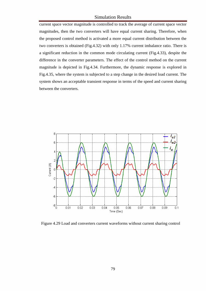
Simulation Results
79
current space vector magnitude is controlled to track the average of current space vector
magnitudes, then the two converters will have equal current sharing. Therefore, when
the proposed control method is activated a more equal current distribution between the
two converters is obtained (Fig.4.32) with only 1.17% current imbalance ratio. There is
a significant reduction in the common mode circulating current (Fig.4.33), despite the
difference in the converter parameters. The effect of the control method on the current
magnitude is depicted in Fig.4.34. Furthermore, the dynamic response is explored in
Fig.4.35, where the system is subjected to a step change in the desired load current. The
system shows an acceptable transient response in terms of the speed and current sharing
between the converters.
Figure 4.29 Load and converters current waveforms without current sharing control

Simulation Results
80
Figure 4.30 Common mode circulating current waveform without current sharing
control
Figure 4.31 Converter current space vector magnitude waveforms without current
sharing control

Simulation Results
81
Figure 4.32 Load and converter current waveforms with average current sharing
control scheme
Figure 4.33 Common mode circulating current waveform with average current
sharing control scheme

Simulation Results
82
Figure 4.34 Converter current space vector magnitude waveforms with average
current sharing control scheme
Figure 4.35 Converters and load current waveforms during step change in the desired
current

Simulation Results
83
4.3.2 Open loop V/f control for three-phase induction motor supplied from parallel
converters based on the average current sharing control method
Figure 4.36 shows block diagram of the proposed control method. In this work, an open
loop V/f control for three-phase induction motor is employed. At any desired speed
(frequency), constant flux, stator current, and torque can be obtained if the V/f ratio is
held constant. However, at a low frequency this approach does not work well due to
stator resistance voltage drop and the necessary rotor slip to produce a torque. For this
reason, these effects should be compensated to achieve high performance regulation at
low speeds. A detailed compensation scheme goes beyond the scope of this thesis and
can be found in [101]. In this work, the motor system supervisor supplies the desired
frequency fref for the drive system. The base modulation index Mbase for the two
converters can be obtained from the M/f mode generator to keep the V/f ratio constant.
The angle ϑ is simply the integration of the required frequency. If the desired speed is
low (below 0.1pu), the M/f mode generator sets Mbase to a constant value that
compensates for the stator resistance voltage drop. Alternatively, at frequencies above
the rated value, the Mbase will be fixed to a value corresponding to the rated voltage, i.e.
field weakening is introduced as the frequency is increased above its base value. Soft
starting of the induction motor is achieved via the ramp function block where a smooth
frequency increment from 0 to the desired frequency (fref ) can be achieved. The base
modulation index (Mbase) is modified in the same manner as the previous application,
such that equal current distribution is maintained.
4.3.2.1 Simulation results for open loop V/f control for three-phase induction
motor supplied from parallel connected converters
A MATLAB/ SIMULINK® model is used to verify the control proposed in Fig.4.36. A
three-phase induction motor with the parameters listed in Table 4.5 is used as a load for
the parallel-connected converters. The converters have the same parameters used in the
previous application.
In accordance with experimental setup, the motor will be tested at an operating voltage
which is different from the rated one. The motor is supplied with 115V at 50Hz since
the converter input voltage is just 150V (200V DC link voltage). Also, the motor load is
adjusted according to the converter current rating. Despite the difference in the physical

Simulation Results
84
parameters and the dead time, the two converters share current evenly, as depicted in
Fig.4.37.
Figure 4.36 Block diagram of open loop V/f for three-phase induction motor based on
the average current sharing control scheme
Parameters Value
Power 2.2kW
Voltage 220-240V
Frequency 50Hz
Speed 2772RPM
Current 8.02A
Power factor 0.85
Table 4.5 Three-phase induction motor parameters
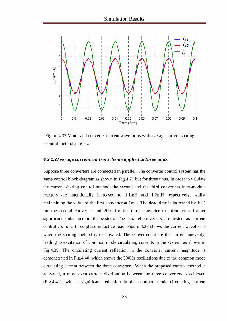
Simulation Results
85
Figure 4.37 Motor and converter current waveforms with average current sharing
control method at 50Hz
4.3.2.2 Average current control scheme applied to three units
Suppose three converters are connected in parallel. The converter control system has the
same control block diagram as shown in Fig.4.27 but for three units. In order to validate
the current sharing control method, the second and the third converters inter-module
reactors are intentionally increased to 1.1mH and 1.2mH respectively, whilst
maintaining the value of the first converter at 1mH. The dead time is increased by 10%
for the second converter and 20% for the third converter to introduce a further
significant imbalance in the system. The parallel-converters are tested as current
controllers for a three-phase inductive load. Figure 4.38 shows the current waveforms
when the sharing method is deactivated. The converters share the current unevenly,
leading to excitation of common mode circulating currents in the system, as shown in
Fig.4.39. The circulating current reflection in the converter current magnitude is
demonstrated in Fig.4.40, which shows the 300Hz oscillations due to the common mode
circulating current between the three converters. When the proposed control method is
activated, a more even current distribution between the three converters is achieved
(Fig.4.41), with a significant reduction in the common mode circulating current
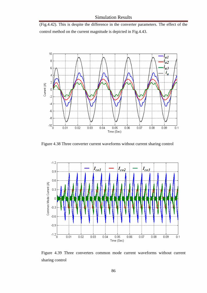
Simulation Results
86
(Fig.4.42). This is despite the difference in the converter parameters. The effect of the
control method on the current magnitude is depicted in Fig.4.43.
Figure 4.38 Three converter current waveforms without current sharing control
Figure 4.39 Three converters common mode current waveforms without current
sharing control
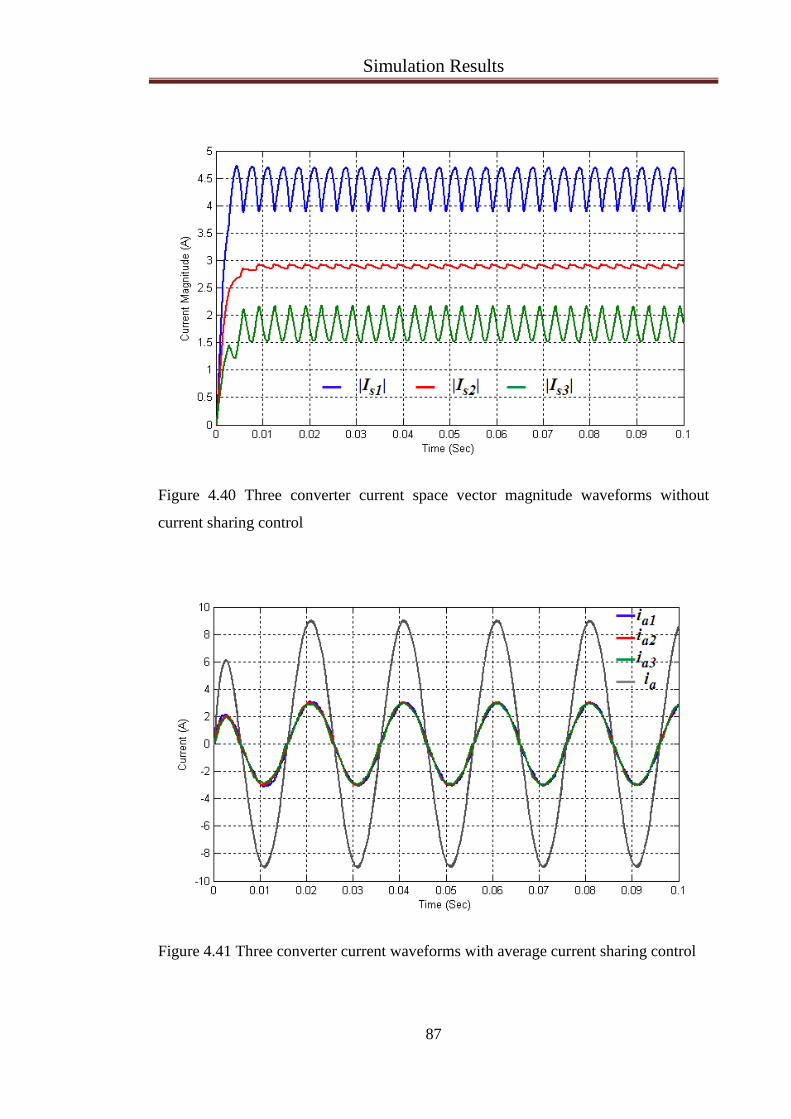
Simulation Results
87
Figure 4.40 Three converter current space vector magnitude waveforms without
current sharing control
Figure 4.41 Three converter current waveforms with average current sharing control

Simulation Results
88
Figure 4.42 Three converter common mode current waveforms with average current
sharing control
Figure 4.43 Three converter current space vector magnitude waveforms with average
current sharing control

Simulation Results
89
4.4 Independent Current Sharing Control Scheme
Based on independent current sharing control strategy, the following sections present
the simulation results for the parallel-connected converters where three, single-phase
current sharing reactors were connected to the output. This scheme will be employed in
the same two applications as applied to the previous method.
4.4.1 Parallel connected converter current-controller based on independent current
sharing control method
Figure 4.44 shows the block diagram for the proposed method when two parallel
connected converters are employed in this application. The converter parameters are
exactly the same as in the average control approach. A MATLAB/ SIMULINK® model
is used to simulate the current sharing between the two converters. The control method
is utilised to control the current in a three-phase inductive load. As previously
mentioned, the current regulator will provide the angle and the base modulation index to
the converter unit. The magnitude of the converter current space vector is calculated,
and its AC component is extracted via a low pass filter. A PI compensator is used to
modify the base modulation index, such that the current magnitude AC component will
track a zero reference value leaving only a DC component in the converter current
magnitudes.
4.4.1.1 Simulation results of parallel-connected converter current controller based on
independent current sharing control
In order to validate the current sharing control method, the second converter sharing
reactors are intentionally increased to 1.1mH, whilst maintaining the value of the
sharing reactors of the first converter at 1mH. Furthermore, the IGBT and diode on
resistances and forward voltage drop for the second converter are increased by 20% as
compared to the first converter. The dead time for the second converter is increased by
20% to introduce a further significant imbalance in the system. When the sharing
method is deactivated, the current waveforms, the common mode circulating current,
and magnitudes of current space vectors will be exactly the same as in section (4.3.1.1).
When the proposed control method is activated a more equal current distribution
between the two converters is achieved (Fig.4.45), with only 0.27% current imbalance

Simulation Results
90
ratio and a significant reduction in the common mode circulating current (Fig.4.46).
This is again despite the difference in the converters parameters. The effect of the
control method on the current magnitude is depicted in Fig.4.47.
Figure 4.44 Block diagram of parallel connected AC/DC/AC converter current
controller based on independent current sharing control

Simulation Results
91
Figure 4.45 Load and converter current waveforms with independent current sharing
control method
Figure 4.46 Common mode circulating current waveform with independent current
sharing control method
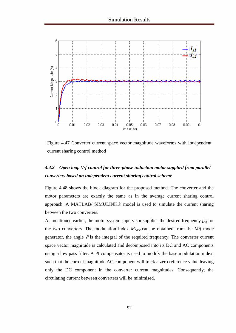
Simulation Results
92
Figure 4.47 Converter current space vector magnitude waveforms with independent
current sharing control method
4.4.2 Open loop V/f control for three-phase induction motor supplied from parallel
converters based on independent current sharing control scheme
Figure 4.48 shows the block diagram for the proposed method. The converter and the
motor parameters are exactly the same as in the average current sharing control
approach. A MATLAB/ SIMULINK® model is used to simulate the current sharing
between the two converters.
As mentioned earlier, the motor system supervisor supplies the desired frequency fref for
the two converters. The modulation index Mbase can be obtained from the M/f mode
generator, the angle ϑ is the integral of the required frequency. The converter current
space vector magnitude is calculated and decomposed into its DC and AC components
using a low pass filter. A PI compensator is used to modify the base modulation index,
such that the current magnitude AC component will track a zero reference value leaving
only the DC component in the converter current magnitudes. Consequently, the
circulating current between converters will be minimised.
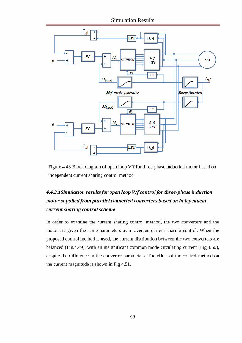
Simulation Results
93
Figure 4.48 Block diagram of open loop V/f for three-phase induction motor based on
independent current sharing control method
4.4.2.1 Simulation results for open loop V/f control for three-phase induction
motor supplied from parallel connected converters based on independent
current sharing control scheme
In order to examine the current sharing control method, the two converters and the
motor are given the same parameters as in average current sharing control. When the
proposed control method is used, the current distribution between the two converters are
balanced (Fig.4.49), with an insignificant common mode circulating current (Fig.4.50),
despite the difference in the converter parameters. The effect of the control method on
the current magnitude is shown in Fig.4.51.

Simulation Results
94
Figure 4.49 Motor and converter current waveforms with independent current sharing
control strategy
Figure 4.50 Common mode circulating current waveform with independent current
sharing control strategy in open loop V/f control for three-phase induction motor

Simulation Results
95
Figure 4.51 Converter current space vector magnitude waveforms for open loop V/f
control for three-phase induction motor based on independent sharing control strategy
4.4.3 Independent current sharing control strategy applied to three units
As in an average current sharing control scheme, the three converters are connected in
parallel to supply a three-phase R-L load. These converters have the structure and
parameters used for the average current sharing control. When the sharing method is
deactivated, the current waveforms, the common mode circulating current, and
magnitudes of current space vectors will be exactly the same as in section (4.3.2.2).
When the independent current sharing control method is activated, a more equal current
distribution between the two converters is resumed (Fig.4.52), with a significant
reduction in the common mode circulating current (Fig.4.53). The effect of the control
method on the current magnitude is shown in Fig.4.54.

Simulation Results
96
Figure 4.52 Three converters current waveforms with independent current sharing
control strategy
Figure 4.53 Three converter common mode current waveforms with independent
current sharing control strategy
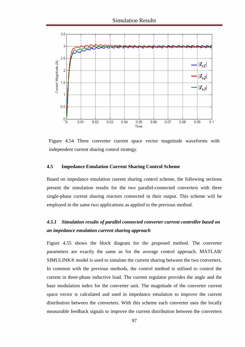
Simulation Results
97
Figure 4.54 Three converter current space vector magnitude waveforms with
independent current sharing control strategy.
4.5 Impedance Emulation Current Sharing Control Scheme
Based on impedance emulation current sharing control scheme, the following sections
present the simulation results for the two parallel-connected converters with three
single-phase current sharing reactors connected in their output. This scheme will be
employed in the same two applications as applied to the previous method.
4.5.1 Simulation results of parallel connected converter current controller based on
an impedance emulation current sharing approach
Figure 4.55 shows the block diagram for the proposed method. The converter
parameters are exactly the same as for the average control approach. MATLAB/
SIMULINK® model is used to simulate the current sharing between the two converters.
In common with the previous methods, the control method is utilised to control the
current in three-phase inductive load. The current regulator provides the angle and the
base modulation index for the converter unit. The magnitude of the converter current
space vector is calculated and used in impedance emulation to improve the current
distribution between the converters. With this scheme each converter uses the locally
measurable feedback signals to improve the current distribution between the converters

Simulation Results
98
independently from the other converters. This scheme can be adopted with any PWM
strategy since it is entirely dependent on the current space vector magnitude. This
approach suffers, however, from a relatively high steady state error, in terms of current
distribution between converters as compared to the previous methods and also the
converter output voltage is affected by the voltage drop on the virtual impedance.
To investigate the scheme operation differences in current sharing reactors, dead time,
switch on resistance, and forward voltage drop are intentionally applied (see section
4.3.1.1). These differences are made in order to show the robustness of the load current
sharing between the two converters. To explore the effect of impedance emulation on
the current distribution, the impedance emulation factor (KZ) is changed from 0 to 0.1,
as shown in Fig.4.56. It can be seen that the current distribution is improved with
increasing impedance emulation factor. However, large values of impedance emulation
factor introduce system oscillations and might push the system into unstable operation.
Figure 4.57 shows the equal current sharing with 2.29% current imbalance ratio when a
suitable impedance emulation factor is selected. The current distribution steady state
error is large compared with previous methods; also, with a suitable impedance
emulation factor, a 70% reduction in common mode circulating current can be achieved
as shown in Fig.4.58. In this case the common-mode circulating current peak value
without current sharing control method is 0.42A. Further investigations are made
through subjecting the system to step change in the desired load current, which can be
seen in Fig.4.59. The two converters show an improved current distribution during
transient conditions regardless of the differences between the two converters.

Simulation Results
99
Figure 4.55 Block diagram of impedance emulation current sharing control scheme
Figure 4.56 Load and converter current waveforms with different impedance
emulation factor
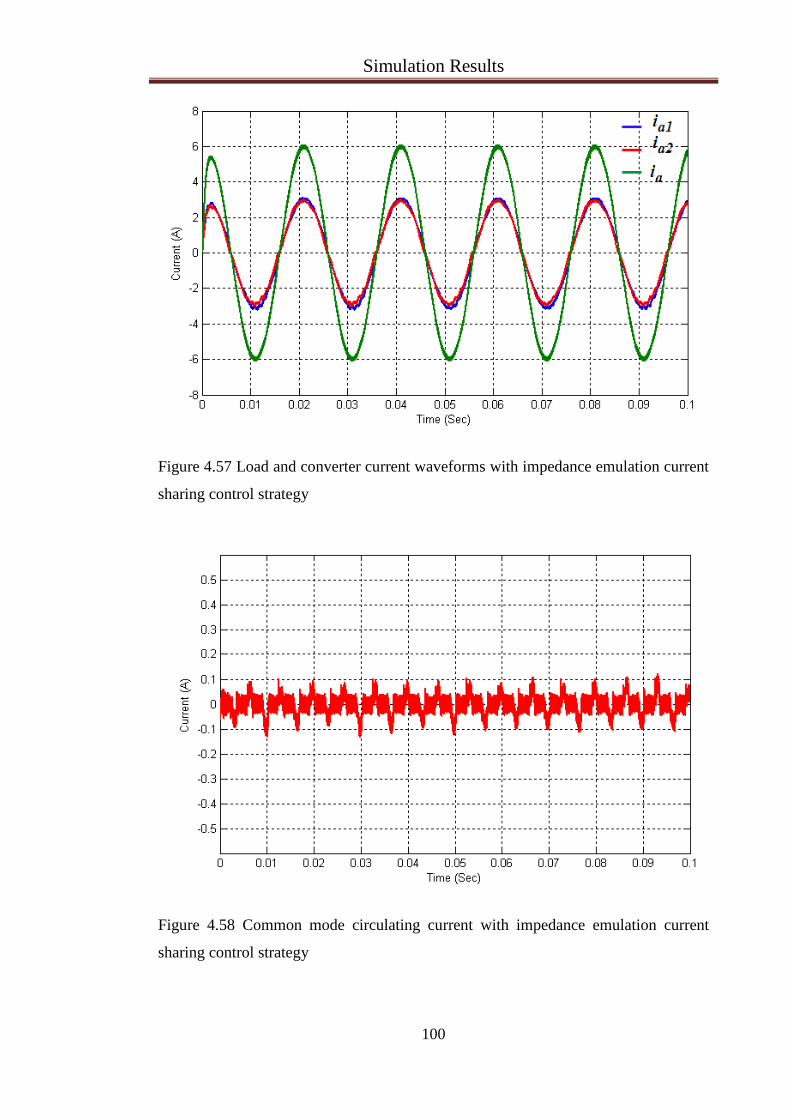
Simulation Results
100
Figure 4.57 Load and converter current waveforms with impedance emulation current
sharing control strategy
Figure 4.58 Common mode circulating current with impedance emulation current
sharing control strategy
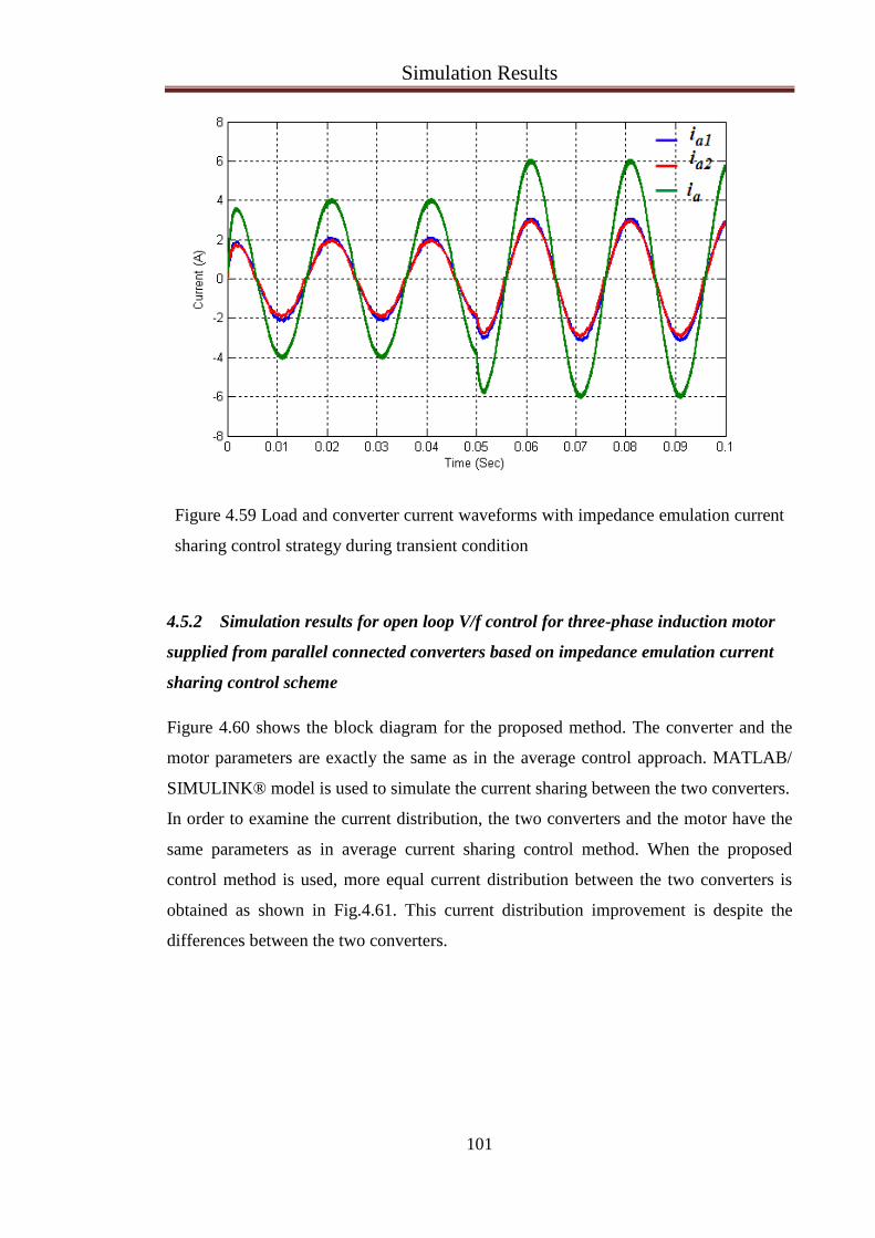
Simulation Results
101
Figure 4.59 Load and converter current waveforms with impedance emulation current
sharing control strategy during transient condition
4.5.2 Simulation results for open loop V/f control for three-phase induction motor
supplied from parallel connected converters based on impedance emulation current
sharing control scheme
Figure 4.60 shows the block diagram for the proposed method. The converter and the
motor parameters are exactly the same as in the average control approach. MATLAB/
SIMULINK® model is used to simulate the current sharing between the two converters.
In order to examine the current distribution, the two converters and the motor have the
same parameters as in average current sharing control method. When the proposed
control method is used, more equal current distribution between the two converters is
obtained as shown in Fig.4.61. This current distribution improvement is despite the
differences between the two converters.

Simulation Results
102
Figure 4.60 Block diagram of an open loop V/f for three-phase induction motor based
on impedance emulation current sharing control strategy
Figure 4.61 Load and converter current waveforms with impedance emulation current
sharing control strategy

Simulation Results
103
4.6 Interleaving Impacts on System Performance
As stated in chapter two, the performance of parallel-connected converters can be
enhanced by using interleaving techniques. This section investigates the impact of
interleaving on two identical parallel-connected AC/DC/AC converters, with separate
but not isolated DC links. Fast Fourier Transform (FFT) analysis is adopted to explore
the impact on the load current harmonics, circulating current harmonics, and the
common mode voltage harmonics. This analysis is applied for both SVPWM and
DPWM strategies with low and high modulation index values.
4.6.1 Combined current
When regular asymmetric SVPWM, is used the harmonic spectra for the combined
(load) current are as shown in Figs.4.62 to 4.65. The first two depict the harmonic
spectra for non-interleaved converters, where the harmonics are centred at multiples of
the carrier frequency. The latter two clarify the harmonic cancellation effect when
symmetrical interleaving is adopted. All the harmonics around the odd multiples of the
carrier frequency are eliminated and accordingly, the current THD. is reduced. Similar
effects are obtained when DPWM strategy is adopted (see appendix B).The current
THD for interleaved and non-interleaved converters is summarised in Table 4.6.
Modulation
index
SVPWM DPWM
THD for
without
interleaving
THD with
interleaving
Non-
interleaved
Interleaved
0.5 2.38 1.63 3.08 1.55
0.9 1.7 1.18 1.72 1.11
Table 4.6 Combined output current THD for different PWM strategies
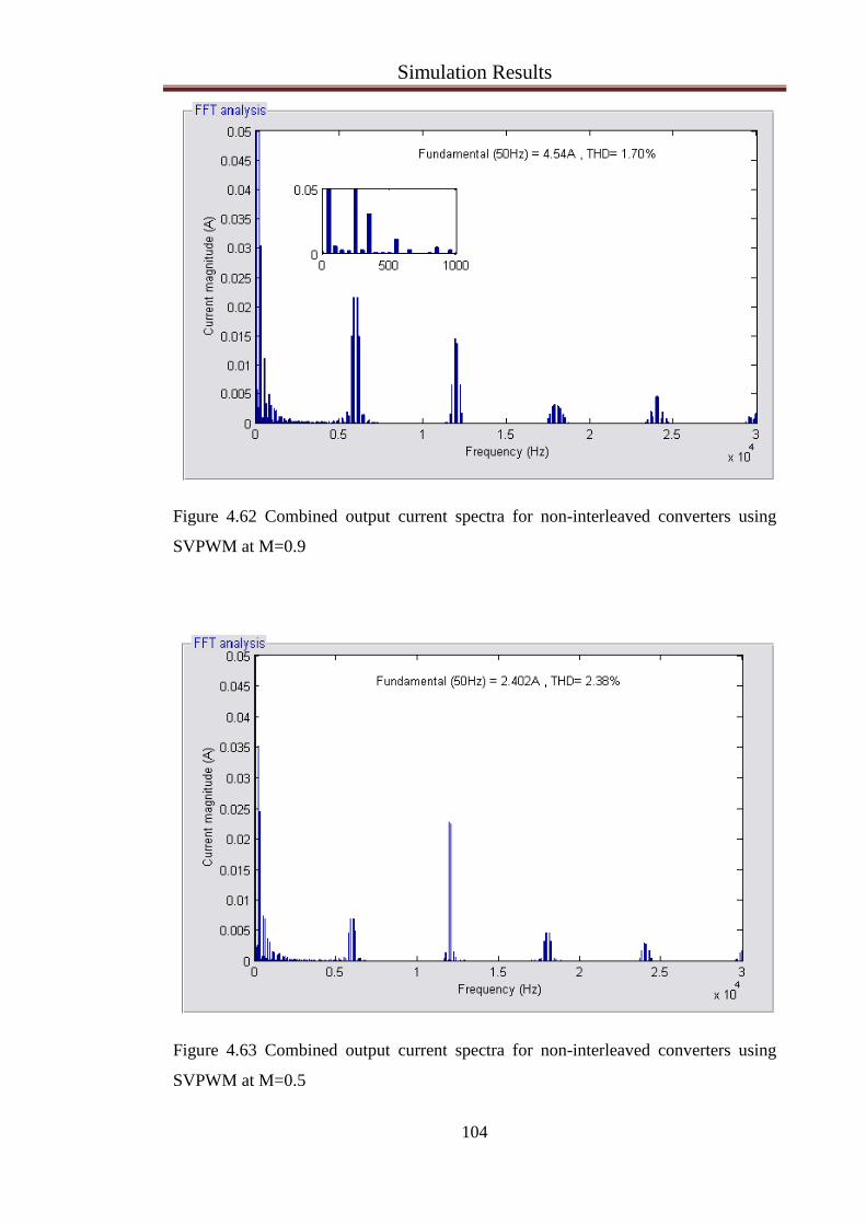
Simulation Results
104
Figure 4.62 Combined output current spectra for non-interleaved converters using
SVPWM at M=0.9
Figure 4.63 Combined output current spectra for non-interleaved converters using
SVPWM at M=0.5

Simulation Results
105
Figure 4.64 Combined output current spectra for interleaved converters using
SVPWM at M=0.9
Figure 4.65 Combined output current spectra for interleaved converters using
SVPWM at M=0.5

Simulation Results
106
4.6.2 Inter-module circulating current
For interleaving, the FFT of the circulating current between the two converters is
presented in Figs.4.66 and 4.67 It can be seen that a dominant high frequency
circulating current is excited between the identical converters. These high frequency
components represent the cancelled harmonics from the combined current spectra due to
the interleaving technique. Unlike the low frequency circulating current components the
high frequency components cannot be controlled by the active current sharing control
methods. Consequently, additional sharing reactors become necessary to limit the high
frequency circulating current.
Similar effects can be monitored when DPWM strategy is adopted (see Appendix B).
Figure 4.66 Circulating current spectra for interleaved converters using SVPWM at
M=0.9

Simulation Results
107
Figure 4.67 Circulating current spectra for interleaved converters using SVPWM at
M=0.5
4.6.3 Common mode voltage
With reference to the parallel-connected AC/DC/AC converters structure, the common
mode voltage is the voltage difference between the neutral point of the load and the
neutral point of the supply. The spectrum of the common mode voltage with non-
interleaved converters that adopt the SVPWM strategy is shown in Figs.4.68 and 4.69.
The harmonic voltage magnitudes are normalised to the DC link voltage. It is clear that
the sideband components that are present differ from the band centre frequency by three
times of the fundamental frequency.
When the two converters are symmetrically interleaved, the odd multiple carrier
sidebands are eliminated as shown in Figs.4.70 and 4.71. Accordingly, in a motor drive
application, this harmonic elimination will actively limit the bearing failure and
electromagnetic interference (EMI) effects that cause nuisance trips in the inverter
drive[102] [103].Similar simulation results are depicted in Appendix B when a DPWM
strategy is employed.

Simulation Results
108
Figure 4.68 Spectra of common-mode voltage for non-interleaved converters with
SVPWM at M=0.9
Figure 4.69 Spectra of common-mode voltage for non-interleaved converters with
SVPWM at M=0.5
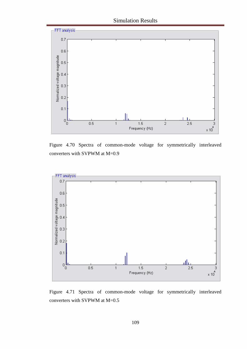
Simulation Results
109
Figure 4.70 Spectra of common-mode voltage for symmetrically interleaved
converters with SVPWM at M=0.9
Figure 4.71 Spectra of common-mode voltage for symmetrically interleaved
converters with SVPWM at M=0.5
Simulation Results
110
4.7 Summary
This chapter presented the SIMULINK models and simulation results for a SVPWM
strategy, a DPWM strategy, and the proposed active current sharing control methods. In
time sharing control strategy, the inter-module current sharing reactors are redundant
and only local information is used by the converters. With this scheme, the switching
losses and heat sink size are reduced. Unfortunately, the method suffers from some
limitations, the first of which is that the paralleled converters should be physically much
closed with a reduced cable inductance which will limit the dv/dt and the system EMI.
The second limitation is that the number of paralleled units cannot easily be increased
since the IGBT devices should be able to handle the peak load current.
The average current control method can be adopted when current sharing reactors are
employed at the output of each converter. This method is modular and can easily be
applied to any number of units without heavy computational capability. The parallel
units share only one piece of information, which is the average of the current space
vector magnitudes.
The third method investigated is quite similar to the average current control method. It
uses the same principle based upon the reflection of circulating currents on the
magnitude of the current space vector. It is a modular and independent method since the
current sharing control of each converter is implemented independently from any of
other converter controllers. However, it has a slightly slower dynamic response when
compared with the average current sharing control method due to employing a LPF in
the control process.
In the final approach, the current distribution was improved through impedance
emulation, instead of increasing physical impedance on the output of each converter.
The emulated impedance value is proportional to the converter current space vector
magnitude, i.e. a large emulated impedance is used when the converter shared current is
large and vice versa. The control algorithm is simple and modular since each converter
is controlled independently from the other converters. Nevertheless, this approach
suffers from a steady state error, in terms of current distribution between the converters.
This steady state error can be significantly reduced with high values of KZ, but this
comes at the cost of an extensive voltage drop increment. For that reason, this scheme is
not recommended for open loop control systems since there is no voltage drop
compensation as in a closed loop control system. The second, third, and fourth methods
can be adopted with any PWM strategy like SPWM, SVPWM, and DPWM since they

Simulation Results
111
are entirely dependent on the converter current space vector magnitude. Also, separate
zero axis circulating current control is unnecessary.
Finally, the impact of interleaving on the performance of the parallel-connected
AC/DC/AC converters has been demonstrated. This included the load current harmonics,
circulating current harmonics, and the common mode voltage harmonics.

Development of Parallel-Connected Converters System
112
Chapter 5. Development of Parallel-Connected Converters System
An AC/DC/AC converter system was implemented to examine the control algorithms
for the parallel operation of the converter units. This chapter describes the hardware and
software development of the prototype parallel-connected converter system. According
to the system structure and requirements of the converter units’ ratings, the
microcontroller, measurement circuits and protection functions have been determined.
Furthermore, this chapter describes the National Instrument LabViewTM
platform which
is employed for monitoring and control.
5.1 System Overview
For experimental convenience, the initial assumption was that two equally rated
parallel-connected, three-phase AC/DC/AC converters with one microcontroller would
provide a suitable platform for investigating the control algorithms. However, in
practice, each converter would have its own microcontroller. The parallel-connected
converter system consists of the following parts:
Two three-phase inverters with individual front end three-phase diode rectifiers
One DSP microcontroller and the necessary interfacing and conditioning circuits
A personal computer (PC)
A communication link between the DSP microcontroller and PC
A three-phase load which is either a three-phase RL load or three-phase
induction motor coupled with a permanent magnet DC generator
Measurement equipment
5.1.1 System requirements
Converter ratings: the three-phase converter ratings are listed in Table 5.1.
DSP Microcontroller requirement: the controller should provide the following:
Six dual PWM units
RS232, JTAG communication interface
At least 12 ADCs for current and voltage sensors

Development of Parallel-Connected Converters System
113
Parameter Value
Voltage 140VRMS
Current 5ARMS
Power capacity 1.2kVA
Output line frequency 0-50Hz
Switching frequency 6kHz
Sampling frequency 12kHz
Table 5.1 AC/DC/AC converter ratings
PC requirement
RS232 compatible ports
A USB port for system debugging
Texas Instruments Code Composer Studio (CCS) debugging software
National Instruments LabViewTM
software for monitoring and control
Measurement Requirements
Voltage and current waveforms measurement.
5.1.2 System structure
The complete structure for the parallel-connected converter system is shown in Fig.5.1.
The grid voltage was accessed via a 5kVA Δ/Y isolating transformer as a power source
for the parallel converters system, i.e. the two converters are supplied from one common
voltage source. Each converter unit includes seven main functional blocks, as shown in
Fig.5.2. These are a three-phase diode rectifier, a three-phase 6-IGBT inverter, a DC bus
filter, three-dual gate drive circuits, current sharing reactors, current transducers and a
voltage transducer. The voltage and current transducers are used to sense the DC link
voltage and the converter output currents to be processed by the microcontroller.
Accordingly, the microcontroller generates the desired PWM signals to control the
output voltage of the converter. Each converter is connected to the load via three single-
phase current sharing reactors to limit the circulating current between the two converters.
The host computer is interfaced with the microcontroller through the USB port which is
used by the CCS software for programming and debugging. Furthermore, the PC is

Development of Parallel-Connected Converters System
114
interfaced to the microcontroller via an isolated RS232 serial link. This serial link is
utilised by the LabViewTM
software for the control and monitoring purposes.
Figure 5.1 Parallel AC/DC/AC converters system structure
Figure 5.2 AC/DC/AC converter structure

Development of Parallel-Connected Converters System
115
5.2 Hardware Implementation
This section presents the hardware design of the parallel-connected converter system in
detail. A picture of the complete test rig is shown in Fig.5.3. The following parts can be
identified:
1. 20A three-phase variac
2. Three-phase circuit breaker and contactor
3. Emergency stop
4. 24V DC power supply
5. AC/DC/AC converter (unit 1)
6. 5kVA three-phase Δ/Y isolation transformer (a detailed description of this can
be found in Appendix A)
7. Host computer (PC)
8. AC/DC/AC converter (unit 2)
9. 2.2kW three-phase induction motor
10. 2.5hp permanent magnet DC generator
11. 10Ω, 10A resistors
12. General purpose power interface board for the Texas Instrument®
TMS320F28335 DSP microcontroller
5.2.1 AC/DC/AC converter unit
The components of each AC/DC/AC converter are shown in Fig.5.4, where the
following parts are found:
1. Three single-phase current sharing reactors
2. Three-phase discrete IGBT inverter with DC link capacitors
3. DC link voltage transducer
4. Three current transducers
5. Three dual gate drive circuits
6. Three-phase diode rectifier
7. Three-phase relay

Development of Parallel-Connected Converters System
116
Figure 5.3 Parallel converters system test rig
Figure 5.4 Hardware structure of the AC/DC/AC converter
Development of Parallel-Connected Converters System
117
The converter components are physically arranged to keep the control signals away
from sources of noise. Also, the DC bus is directly connected to the IGBTs to reduce
the parasitic inductance and the devices turn off voltages. Furthermore, PWM signal
and transducers cables are kept as short as possible and placed away from the power
cables to minimise the influence of noise. Detailed converter components design and
selection are given below:
Three-phase rectifier and DC-bus
A three-phase diode rectifier (2MT60) is used, 5A input fuses along with
thermistors provide DC link inrush current protection. Furthermore, this rectifier
is connected to the input supply through a three pole relay which is controlled by
the microcontroller.
It is worth mentioning that electrolytic and film capacitors are commonly used
in the DC bus of an inverter. Electrolytic capacitors have a high capacitance to
volume ratio and a lower price when compared with film capacitors. However,
they have a higher equivalent series resistance (ESR) and lower current ripple
rating. In view of this, electrolytic capacitors are selected for this work. The
capacitors’ size can be determined with the following steps:
Estimate the capacitor size according to the desired voltage ripple Vripple
using the following equation [104]:
5.1
Where Pload is the load rated power, Vs-rms the rectifier input voltage, and
frec the frequency of the input voltage.
Compute the power dissipation of the selected capacitor. This requires
information about the dominant current ripple components. The current
ripple components imposed by the rectifier and inverter can be obtained
with the aid of digital simulation or through 3-D look up graphics based
on spectral analysis[105]. With an SVPWM strategy the capacitor
current ripple contribution caused by the inverter IC,rms,I is calculated as
[106] [107]:

Development of Parallel-Connected Converters System
118
5.2
Where α is the load angle and Irms is the rms value of the load current.
The dominant harmonic component of this current ripple occurs at twice
the switching frequency.
The diode rectifier harmonic current IC,rms,R is dominantly the sixth
harmonic, which is approximated as Pload/10Vs-rms [104]. Accordingly, the
total current rms value will be:
5.3
A combination of series and parallel capacitors will be selected to handle
the required current ripple Ic,rms. The capacitor power dissipation Pd is
calculated considering the two current ripple components and the ESR
value at the dominant harmonic frequency.
5.4
Where, RESR_fdI and R_ESR_fdR are the ESRs at the dominant current ripple
frequency contributed by the inverter and rectifier sides respectively.
Calculate the capacitor core temperature using the equation below:
5.5
Where, Tc and Ta are the capacitor core and the ambient temperature
respectively, and Rth is the capacitor core to case thermal resistance
measured in C˚/W. If the capacitor core temperature Tc does not match
the permissible limit, the number of capacitor parallel branches should be
increased to satisfy this limit.
Using the above mentioned procedure with 2%Vdc voltage ripple, the
DC-bus requires two series-connected 680µF, 200V electrolytic
capacitors.

Development of Parallel-Connected Converters System
119
Due to the capacitor leakage resistance, unequal voltage will be on the
individual series capacitors. To overcome this problem, each capacitor
must be shunted with a balancing resistor. The resistor value should be
much smaller than the leakage resistance, which is calculated from
knowledge of the leakage current and operating voltage [108]. Using the
selected capacitor datasheet, the leakage current is calculated and
accordingly a 10kΩ, 3W balancing resistor is used.
The DC link capacitors are connected to the inverter via a low inductance
laminated bus bar to reduce the parasitic inductance. A 150nF high
frequency metallised polypropylene film snubber capacitor was
connected between the DC link terminals to provide a low-impedance
path for high frequency current components and to suppress the turn off
transient voltages.
Switching devices
Six IGBTs (IRG7PH35UD1PBF) are used in the three-phase inverter
construction. These devices have a voltage and current rating of 1200V and 20A
respectively. High voltage and current margins are provided through these
devices to ensure flexible testing capability.
Transducers
Three current transducers (HXS 20-NP/SP30) are used to sense the three-phase
output current of each converter. The transducer output signal is conditioned and
processed by the control board for the control and hardware protection functions.
Also, a voltage transducer (LV 25-P) is employed for DC link voltage
measurement and is utilised by the microcontroller for monitoring and
overvoltage protection purposes.
Current sharing reactors
Three single-phase current sharing reactors are connected to the output of the
converter. The minimum inductor value required to maintain safe operation of
the parallel system is [67]:
5.6
Development of Parallel-Connected Converters System
120
Where Δt is the switching edge misalignment and Δ is the maximum
allowable current change caused by switching edge misalignment. For the
hardware system under test, the two converters are synchronised in terms of the
fundamental and carrier frequency. However, there is a switching edge
misalignment of about 1-2µsec. Accordingly, three 1mH single phase reactors
are connected to the output of each converter to suppress the circulating current
to acceptable limit.
Gate drive circuit
The functions of the driver circuit are amplifying the (ON/OFF) logic signals
and delivering the required peak current to the IGBT gate at switching. It also
detects a device short circuit through monitoring the voltage between the
collector and emitter (VCE) of the IGBT during the turning on period.
Each converter unit involves three dual gate drive circuits. The gate drive circuit
is based on HCPL-316J, which is a two Ampere gate drive optocoupler with
integrated (VCE) desaturation detection and fault status feedback. During a short
circuit fault, as the current increases, the VCE (sat) increases, when the VCE (sat)
reaches the preset threshold level a fault is detected. The gate driver then
performs a soft turn-off of the IGBT. The fault pin status is pulled to low for the
purpose of notifying the DSP microcontroller of the fault condition. To clear the
fault condition, the RESET pin should be pulled low by the microcontroller. In a
similar manner, if the output voltage of the gate driver is not sufficient to turn on
the IGBT, another fault condition is detected by the gate drive circuit. More
details for the HCPL-316J are given in [109]
A complete schematic diagram of the dual gate driver circuit is given in
Figs.5.5a and 5.5b.
5.2.2 General purpose power interface board for the Texas Instrument®
TMS320F28335 DSP microcontroller
The general purpose interface board designed at Newcastle University is shown in
Fig.5.6. This board represents the interface between the Spectrum Digital F28335eZdsp
and the power converter hardware.
Based on the Texas Instrument® TMS320F28335 device, the control board brings
floating-point processing to a real time power control application. The Texas

Development of Parallel-Connected Converters System
121
Instrument® TMS320F28335 is the first floating point digital signal controller that
provides 150MHz operation and includes an IEEE-754 Single-Precision Floating-Point
Unit (FPU). The availability of floating point arithmetic saves development time by
eliminating scaling and adjustment for numerical resolution. As it is designed mainly
for industrial applications, the F28335 has plenty of peripheral circuits. For example,
the 16-channel 12-bit ADC, six dual channel PWM units, and an encoder interface
which can be used for motor control purposes. Different communication links such as
the serial communication interface (SCI), the serial peripheral interface (SPI), the
multichannel buffered serial port (McBSP) module, and the inter-integrated circuit (I2C)
are available. The Texas Instrument® TMS320F28335 provides a joint test action group
(JTAG) interface, which supports real-time debugging. With the help of the JTAG, the
user can watch and modify the contents of the memory and the registers without
stopping the processor. The physical memory of the ezdspTM
F28335 is comprised of
68K bytes of on-chip RAM, 512K bytes of on-chip Flash memory, and 256K bytes of
off-chip SRAM memory. Full details of the Texas Instrument® TMS320F28335 can be
found in [110] [111].
(a)

Development of Parallel-Connected Converters System
122
(b)
Figure 5.5 Dual gate drive circuit schematic diagram (a) For Top IGBT (b) For bottom
IGBT
The general purpose interface board is designed for applications requiring a single board
solution. It can be used in grid-tie inverters, AC induction motor drives, PMSM motor
drives, brushless DC motor drives, wind turbine control, testing of two parallel-
connected three-phase converters, etc. The interface board provides the following
functions:
Auxiliary power supply unit
The on board Auxiliary power supply provides +15V,-15V, and +5V.
These voltages are used by all the on board power electronics interfaces
and any off-board interfaces such as current sensors, voltage sensors,
shaft encoder, and gate drive circuits.
Analogue signals interface
The general interface board includes all the necessary conditioning and
protection circuits such that the analogue signals can be processed safely
by the ADC input of the ezdsp board. As the ezdsp has 16 analogue
inputs, ten of these signal interfaces are prepared to be utilised by the
Development of Parallel-Connected Converters System
123
current and voltage sensors. The rest of the analogue inputs are available
for any other analogue inputs.
To provide fast hardware protection, six of the sensor interfaces are
combined with an out-of-range trip circuit. This facility can be easily
devoted to over-current or over-voltage protection. The upper and lower
trip threshold can be adjusted via variable resistors. The outputs of the
out-of-range circuits are wired so that any out of range condition will
produce logic zero output. This output is connected to the
microcontroller Trip-Zone input. The microcontroller can be configured
to switch off all the PWM outputs when the Trip-Zone input is low.
In this work, eleven analogue input signals are applied to the general
interface board. These signals are the converter currents signals, the
combined (load) current signals, and the DC link voltage of the two
converters. The sensor out-of-range trip circuit is utilised for over-
current protection for the two parallel- connected converters.
Gate drive interface
This interface connects the six pairs of PWM units which are provided
by the Texas Instrument® TMS320F28335 to the gate drive circuits.
This interface allows the fault pin status of the gate drive circuit to be
monitored by the microcontroller so that suitable actions can be carried
out in the event of a fault. The interface transfers the fault reset signal
from the microcontroller to the gate drive circuit to clear the fault
condition.
Relay circuit interface
Four DSP general purpose input output (GPIO) pins can be configured as
output to control four on board relays. The GPIO output drives a
MOSFET gate, while the relay coil is energised via the MOSFET drain.
These relay circuits can be utilised to control larger relays or contactors.
In this work, two relays are employed to control larger three-phase relays
which switch on/off the main power to the converters.
The general interface board provides other functions such as digital to
analogue conversion and a shaft encoder interface which are not used in
this work.

Development of Parallel-Connected Converters System
124
Figure 5.6 General interface board with the Texas Instrument® TMS320F28335 DSP
microcontroller
5.2.3 Test load
Two types of load are used to test the parallel-connected converter system. The first is a
three-phase RL load. This load includes three 10Ω, 10A rheostats and three 10mH, 10A
centre-tap inductors. The second type of load is a three-phase induction motor coupled
to a permanent magnet DC generator which is in turn loaded with three series connected
10Ω,10A rheostats. The induction motor parameters are 2.2kW, 2pole, 220V, 8.02A,
2770 RPM, 0.85 pf. The DC generator has the following parameters: 2.5hp, 130V,
3000RPM.
5.3 Implementation of control algorithms
This section presents a brief explanation of the proposed control algorithms. The
programs have been written in C-language using Code Composer Studio (CCS3.3)
software development tools. Monitoring and control functions were implemented in the
LabViewTM
graphical oriented programming language.

Development of Parallel-Connected Converters System
125
5.3.1 LabViewTM
environment
Figure 5.7 shows the LabViewTM
control and monitoring panel. The communication
between the Texas Instrument® TMS320F28335 DSP microcontroller and the host
computer is based on the principle of polling and is achieved via the RS232 serial
interface. Every 0.2Sec a control data package is sent to the microcontroller. In response,
the microcontroller sends a data package back to the host computer. The main control
data that the microcontroller receives from the LabViewTM
panel is:
Switching commands: the main input power to the three-phase converters is
controlled by three-phase relays. The relay coil is energised through a small on
board relay controlled by the microcontroller
Gate drive enable: the PWM outputs for each converter can be enabled or
disabled individually through sending commands from the panel to the
microcontroller
System operation mode: the system operation mode can be changed easily from
open loop to closed loop via the control panel
Reference setting: the desired output frequency (speed with machine load), the
desired rotating reference frame currents, and the base modulation index values
in open loop mode
Compensator parameters: all the PI compensator parameters (kp and ki) can be
adjusted in real time
The information that is received from the DSP microcontroller and monitored
through the LabviewTM
panel is:
The system operation mode whether open loop or closed loop
The interrupt service routine (ISR) execution time
The DC link voltage: the ADC readings of the DC link voltage sensors are
scaled and monitored by the LabViewTM
panel
The current waveform: the converter currents and the load current in both the
stationary and rotating reference frame are stored in the internal or external ram
of the DSP microcontroller. The storing speed depends on the desired output line
frequency. For 50Hz, one value is stored every two ISRs, i.e. 6k sample/sec. For
10Hz, one value every four ISRs is stored, i.e. 3k sample/sec. The stored data is
then downloaded at low speed to the LabViewTM
panel. The transient response

Development of Parallel-Connected Converters System
126
due to the step change in the desired frequency (speed in machine load) or the
desired current can easily be captured using the same approach.
Figure 5.7 LabViewTM
control and monitoring panel
5.3.2 Algorithm of time sharing control scheme
Figure 5.8 shows the flowchart of time sharing control scheme. It can be seen that the
program starts with variable declaration, the initialisation of peripherals, timers and
interrupt service routines. The timers are configured to create the triangular output with
a frequency equal two times the required switching frequency (in accordance with the
number of parallel units). The triangular output was used for PWM generation and ADC
converter synchronisation. The ADC was synchronised to the peak of the triangular
carrier.
After receiving all the reference values, modes of operation, and the PI compensator
parameters, the ADC is triggered. The three-phase currents and the DC link voltage of
the two converters are converted to its digital equivalent.

Development of Parallel-Connected Converters System
127
Figure 5.8 Flowchart of time sharing control algorithm
After the A/D conversion, the program jumps into the ISR. During each ISR, the three-
phase currents and DC link voltage for the converters are calculated. The offset imposed
by the sensors or the conditioning circuits is compensated for. If the number of ISRs is
odd, the first converter current space vector magnitude is calculated and compared with
the reference value. A PI compensator function is called to process the error signal and
produces the desired modulation index. The Backward-Euler algorithm was utilised in
discretisation of the analogue PI compensator. To avoid over-modulation and integrator
windup, the PI compensator output value and the integrator output value are limited to a
specified value. However, the new PWM duty ratio will not be updated until the next
even numbered ISR.
Accordingly, the situation will be opposite with respect to the second converter. The
desired modulation index is calculated when the ISR number is even and the PWM duty
is updated in the next odd numbered ISR.

Development of Parallel-Connected Converters System
128
5.3.3 Algorithm of average current sharing control scheme in a current controller
application
Figure 5.9 shows the flowchart of the average current sharing control scheme. As in the
previous flowchart, the program starts with variable declaration, initialisation of
peripherals, timers and interrupts service routines. The timers are set to generate a
triangular carrier with frequency equal to the switching frequency. The triangular output
is used for PWM generation and ADC converter synchronisation. The ADC
synchronises with the peak and the valley, i.e. the sampling frequency is twice the
switching frequency. After the end of each ADC process, the program jumps to the ISR.
During each ISR, the three-phase currents and the DC link voltage for the converters are
calculated. Only two phase load currents are measured and calculated instead of all
three-phases. During the current and voltage calculation, the offset due to the sensors or
conditioning circuits is compensated for.
The next step is the application of Clark and Park transforms to the load current. Then,
the function dq current regulator is called to generate the base modulation index and
angle, according to the rotating reference frame current demands. The base modulation
index and angle are used by the converters as base values.
The current space vector magnitude for the two converters (|Is1| and |Is2|) and their
average value (|Isavg|) are then calculated. The errors ((|Is1|-|Isavg|) and (|Is2|-|Isavg|)) are
used as inputs to the PI compensator function to produce the desired modification in the
base modulation index value for each converter, to achieve equal current sharing.

Development of Parallel-Connected Converters System
129
Figure 5.9 Flowchart of average current sharing control algorithm employed in a
current controller application
5.3.4 Algorithm of open loop V/f control for three-phase induction motor supplied
from parallel converters based on the average current sharing control scheme
The algorithm for this application is similar to the previous one; however, the base
modulation index and the angle calculations are different. The angle is simply
calculated from the integral of angular speed ω. The base modulation index, which
controls the voltage magnitude, is calculated such that the ratio M/f is constant. This
ratio represents the modulation index at rated voltage to rated frequency. However,
when the frequency and hence the modulation index and the stator voltage are low, the
stator resistance voltage drop cannot be neglected and must be compensated for.
Furthermore, at frequencies higher than the rated, the stator voltage and hence the
modulation index must not increase the rated value.
Figure 5.10 demonstrate the flowchart for the average current sharing control scheme
when employed in an open loop V/f speed control of induction motor.

Development of Parallel-Connected Converters System
130
Figure 5.10 Flowchart of average current sharing control algorithm employed in open
loop V/f control
5.3.5 Algorithm for independent current sharing control scheme in a current
controller application
When an independent current sharing control method is adopted instead of the average
current sharing control, the algorithm flowchart will be as shown in Fig.5.11. It can be
seen from the flowchart that this is quite similar to that shown in Fig.5.9; however, the
method of modifying the base modulation index requires calling a second order
Butterworth low pass filter function. The difference equation for such a filter, designed
using the bilinear transform method mentioned in the previous chapter, is shown in (5.7).
A 50Hz corner frequency and 12 kHz sampling frequency were considered.
5.7

Development of Parallel-Connected Converters System
131
The AC component of the current space vector magnitude is isolated with the aid of the
LPF and then controlled to zero by a PI compensator. The output of the PI compensator
is used to modify the base modulation index such that the AC component of the current
space vector magnitude is minimised.
Figure 5.11 Flowchart of independent current sharing control employed in a current
controller application
5.3.6 Algorithm for open loop V/f control for three-phase induction motor supplied
from parallel converters based on independent current sharing control scheme
Figure 5.12 clarifies the algorithm flowchart for the independent current sharing control
strategy when employed in an open loop V/f control. The flowchart is somewhat similar
to that of the average current sharing control shown in Fig.5.10. The LPF filter function
is used in modifying the modulation index, as in the previous flowchart.
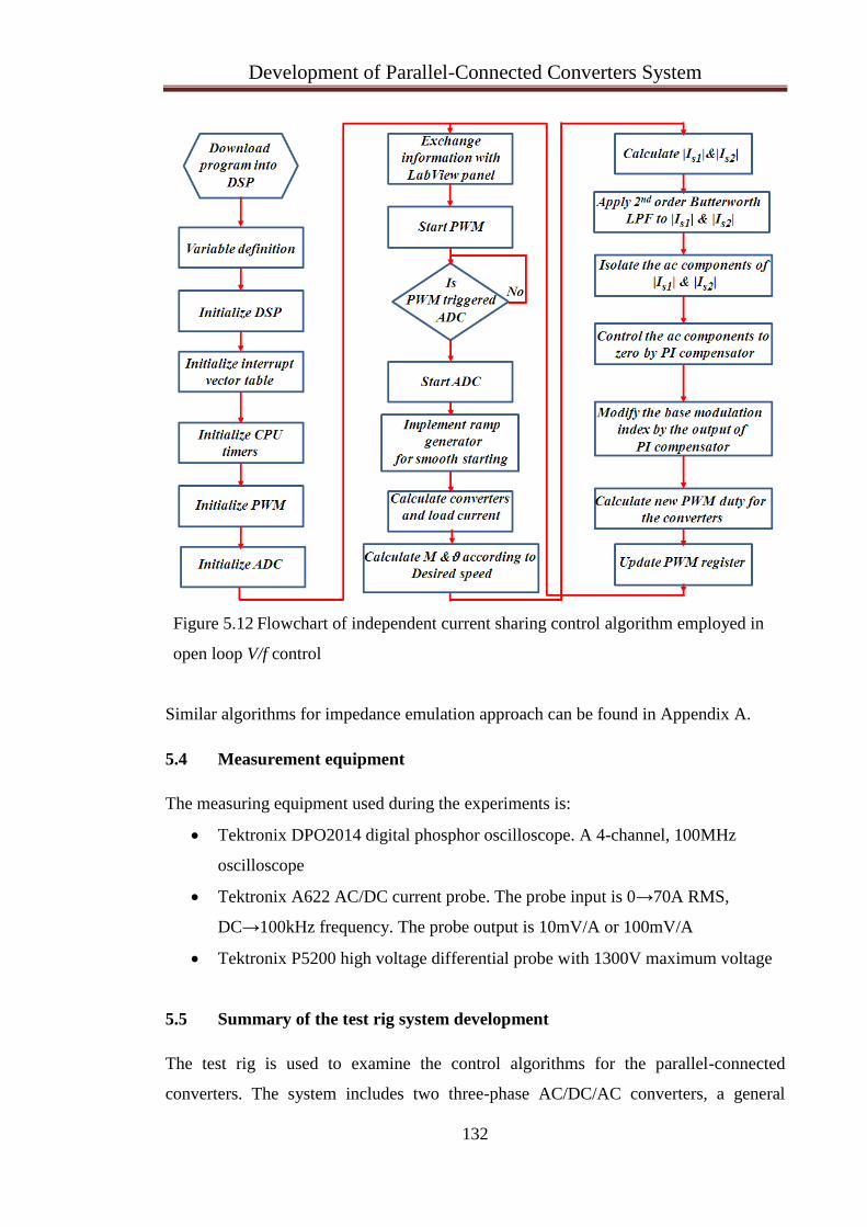
Development of Parallel-Connected Converters System
132
Figure 5.12 Flowchart of independent current sharing control algorithm employed in
open loop V/f control
Similar algorithms for impedance emulation approach can be found in Appendix A.
5.4 Measurement equipment
The measuring equipment used during the experiments is:
Tektronix DPO2014 digital phosphor oscilloscope. A 4-channel, 100MHz
oscilloscope
Tektronix A622 AC/DC current probe. The probe input is 0→70A RMS,
DC→100kHz frequency. The probe output is 10mV/A or 100mV/A
Tektronix P5200 high voltage differential probe with 1300V maximum voltage
5.5 Summary of the test rig system development
The test rig is used to examine the control algorithms for the parallel-connected
converters. The system includes two three-phase AC/DC/AC converters, a general

Development of Parallel-Connected Converters System
133
purpose power interface board based on the Texas Instrument® TMS320F28335 DSP
microcontroller, test loads, and measurement equipment.
The AC/DC/AC converter hardware design has been considered and the converter
component selection and arrangement has been described. Issues concerned with the
control algorithm implementation have also been explained.
The general interface board for the Texas Instrument® TMS320F28335 DSP
microcontroller is described in general and a detailed explanation of the utilised
functions in this work has been presented.
The test loads and the measurement equipment that were used in obtaining experimental
results have been described. A simple graphical user interface was developed in the
National Instruments LabViewTM
environment. This user interface provided PC
monitoring and program control and simple result collection during transient and steady
state conditions.
Detailed circuit diagrams for the parallel connected converter system are given in
Appendix A.
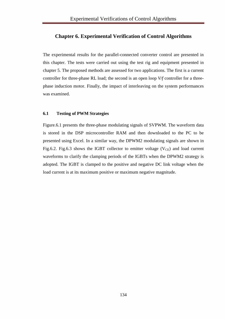
Experimental Verifications of Control Algorithms
134
Chapter 6. Experimental Verification of Control Algorithms
The experimental results for the parallel-connected converter control are presented in
this chapter. The tests were carried out using the test rig and equipment presented in
chapter 5. The proposed methods are assessed for two applications. The first is a current
controller for three-phase RL load; the second is an open loop V/f controller for a three-
phase induction motor. Finally, the impact of interleaving on the system performances
was examined.
6.1 Testing of PWM Strategies
Figure.6.1 presents the three-phase modulating signals of SVPWM. The waveform data
is stored in the DSP microcontroller RAM and then downloaded to the PC to be
presented using Excel. In a similar way, the DPWM2 modulating signals are shown in
Fig.6.2. Fig.6.3 shows the IGBT collector to emitter voltage (VCE) and load current
waveforms to clarify the clamping periods of the IGBTs when the DPWM2 strategy is
adopted. The IGBT is clamped to the positive and negative DC link voltage when the
load current is at its maximum positive or maximum negative magnitude.

Experimental Verifications of Control Algorithms
135
Figure 6.1 Experimental SVPWM modulating signals
Figure 6.2 Experimental DPWM2 modulating signals

Experimental Verifications of Control Algorithms
136
Figure 6.3 Experimental load current and IGBT collector to emitter voltage (2A/div;
100V/div; 10msec/div)
6.2 Testing of Time Sharing Approach
Using the parallel-connected converter system described in the previous chapter, the
time sharing approach was examined experimentally with the SVPWM strategy. The
two converters were directly paralleled without using current sharing reactors. In
accordance with simulation results, the two converters were used as a current controller
for a three-phase RL load. Unlike the other proposed methods, the system was tested
with only 120V DC link voltage, due to a high noise level which triggers the fault
protection on the gate drive circuit. Also, high voltage and current spikes sometimes
activate the protection circuit.
Figure 6.4 shows the converter and load current waveforms during the steady state
condition when the desired load current magnitude is 4A. The two converters have the
same current magnitudes and each converter supplies currents for only half of a
switching cycle. The current controller produced the desired load current magnitude. To
examine the transient performance, the converters were subjected to a step change in the
desired current magnitude. Equal current sharing between the converters and fast
transient response are depicted in Fig.6.5.

Experimental Verifications of Control Algorithms
137
Figure 6.4 Experimental steady state converter and load currents with time sharing
approach (5A/div; 20msec/div)
Figure 6.5 Transient converter and load currents with time sharing approach (2A/div;
20msec/div)

Experimental Verifications of Control Algorithms
138
6.3 Testing Average Current Sharing Control Scheme
The two parallel converters were used to examine the proposed algorithms with 1mH
current sharing reactors and a 200V DC link voltage. As mentioned in the simulation
results discussion, the system was tested in two applications. The first was a current
controller for a three-phase RL load, with different frequencies in both transient and
steady state conditions. The second was an open loop V/f control for a three-phase
induction motor with frequency range of 10Hz to 50Hz. The first test was conducted
with both SVPWM and DPWM2 strategies. The following results are related to
SVPWM and those related to DPWM2 are presented in Appendix C.
6.3.1 Current controller for the three-phase RL load
To demonstrate the current sharing capability, imbalance in the current sharing reactors
and dead times was deliberately introduced. To achieve this, a 0.1mH inductor was
added in series with the 1mH current sharing reactors of the second converter and a 20%
increment in the second inverter dead time relative to the first converter was applied (in
common with the values used in simulations). Figure 6.6 shows the converter and load
current waveforms when the sharing control method was deactivated. The current
sharing between the converters is unequal and exceeds acceptable limits. Significant
distortion appears in the converter current waveforms. The difference in current
produced by the two modules relative to the total current supplied is referred to as the
“current imbalance ratio”. In this case, it has a value of 37.7%, a level of imbalance
which may lead to uneven thermal stress and device failure.
The common-mode current and the converter current space vector magnitudes were
calculated within the algorithm and stored in the microcontroller RAM. With the aid of
the LabViewTM
panel, the stored data was copied to a text file, and then processed by
the Excel software. The common mode current and the current space vector magnitudes
are depicted in Figs.6.7 and 6.8 respectively.
Figure 6.9 shows the load and converter currents when the average current sharing
control was used. Excellent current sharing is achieved with minimum distortion in the
current waveform. The current imbalance ratio between the converters is reduced from
37.7% to 3.34% of the total current. The effect of the control method on the common
mode current and the current space vector magnitudes is presented in Figs.6.10 and 6.11,
respectively. The common mode circulating current reduction is greater than 45% and

Experimental Verifications of Control Algorithms
139
the converter current space vectors closely track the average of converter current space
vectors.
Figure 6.6 Experimental converter and load current waveforms without sharing
control at 50Hz (2A/div; 10msec/div)
Figure 6.7 Experimental common-mode circulating current without sharing control

Experimental Verifications of Control Algorithms
140
Figure 6.8 Experimental current space vector magnitudes without sharing control
Figure 6.9 Experimental converter and load current waveforms with average current
sharing control at 50Hz (2A/div; 10msec/div)

Experimental Verifications of Control Algorithms
141
Figure 6.10 Experimental common-mode circulating current with average current
sharing control
Figure 6.11 Experimental current space vector magnitude waveforms with average
current sharing control
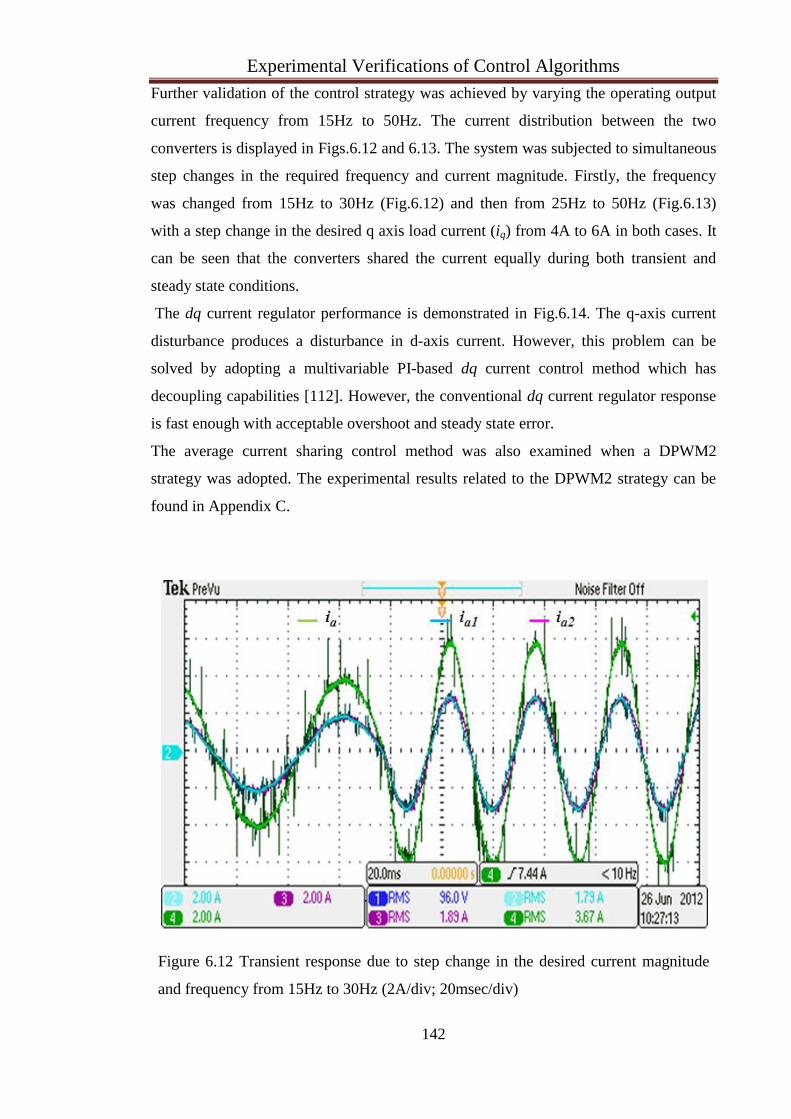
Experimental Verifications of Control Algorithms
142
Further validation of the control strategy was achieved by varying the operating output
current frequency from 15Hz to 50Hz. The current distribution between the two
converters is displayed in Figs.6.12 and 6.13. The system was subjected to simultaneous
step changes in the required frequency and current magnitude. Firstly, the frequency
was changed from 15Hz to 30Hz (Fig.6.12) and then from 25Hz to 50Hz (Fig.6.13)
with a step change in the desired q axis load current (iq) from 4A to 6A in both cases. It
can be seen that the converters shared the current equally during both transient and
steady state conditions.
The dq current regulator performance is demonstrated in Fig.6.14. The q-axis current
disturbance produces a disturbance in d-axis current. However, this problem can be
solved by adopting a multivariable PI-based dq current control method which has
decoupling capabilities [112]. However, the conventional dq current regulator response
is fast enough with acceptable overshoot and steady state error.
The average current sharing control method was also examined when a DPWM2
strategy was adopted. The experimental results related to the DPWM2 strategy can be
found in Appendix C.
Figure 6.12 Transient response due to step change in the desired current magnitude
and frequency from 15Hz to 30Hz (2A/div; 20msec/div)
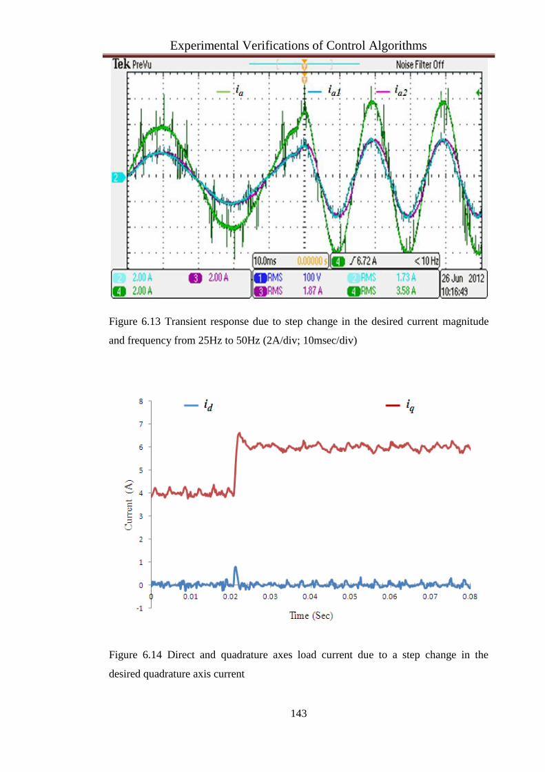
Experimental Verifications of Control Algorithms
143
Figure 6.13 Transient response due to step change in the desired current magnitude
and frequency from 25Hz to 50Hz (2A/div; 10msec/div)
Figure 6.14 Direct and quadrature axes load current due to a step change in the
desired quadrature axis current

Experimental Verifications of Control Algorithms
144
6.3.2 Open loop V/f control for a three-phase induction motor
Instead of a three-phase RL load, a three-phase induction motor was connected as a load.
An open loop V/f speed control was adopted for further validation of the average current
sharing control method. The three-phase induction motor was rated at 230V-240V
which is beyond the parallel converter system voltage rating. Accordingly, a virtual
induction motor rating was assumed to be 120V at 50Hz.
As mentioned in the previous section, considerable circulating currents were produced
when using different sharing reactors and dead time for the two converters.
Consequently, when the current sharing control was deactivated, unequal current
distribution (53.95% imbalance ratio) between the two converters was present, as shown
in Fig.6.15. Also, considerable common mode circulating currents were excited
between the converters as shown in Fig.6.16.
When the average current sharing control was activated, the current imbalance ratio was
reduced from 53.95% to 0.2%, as demonstrated in Fig.6.17. Moreover, Fig.6.18 shows
that the common-mode circulating current was reduced to 40% of its value when the
sharing control was not employed. Figure 6.19 demonstrates the soft starting of
induction motor. The converter line frequency is increased smoothly from 0Hz to the
desired frequency to avoid excessive motor starting current.
Figure 6.15 Experimental converter and motor current waveforms without sharing
control when the desired frequency is 50Hz (2A/div; 10msec/div)

Experimental Verifications of Control Algorithms
145
Figure 6.16 Experimental common-mode circulating current without sharing control
when the desired frequency is 50Hz
Figure 6.17 Experimental converter and motor current waveforms with average
current sharing control when the desired frequency is 50Hz (2A/div; 10msec/div)

Experimental Verifications of Control Algorithms
146
Figure 6.18 Experimental common-mode circulating current with sharing control
when the desired frequency is 50Hz
Figure 6.19 Three-phase motor current during soft starting (2A/div; 1sec/div)

Experimental Verifications of Control Algorithms
147
The average current sharing control was also assessed when the command frequency
was 20Hz and 30Hz (Figs.6.20 and 6.21). It is clear that the two converters still share
the motor current equally regardless of the line command frequency reduction, the
differences in sharing reactors and differences in dead time values.
For further confirmation, the current waveforms for the average current sharing control
scheme were also collected using the LabViewTM
panel; these can be found in Appendix
C.
Figure 6.20 Experimental converter and motor current waveforms with average
current sharing control when the desired frequency is 20Hz (2A/div; 20msec/div)
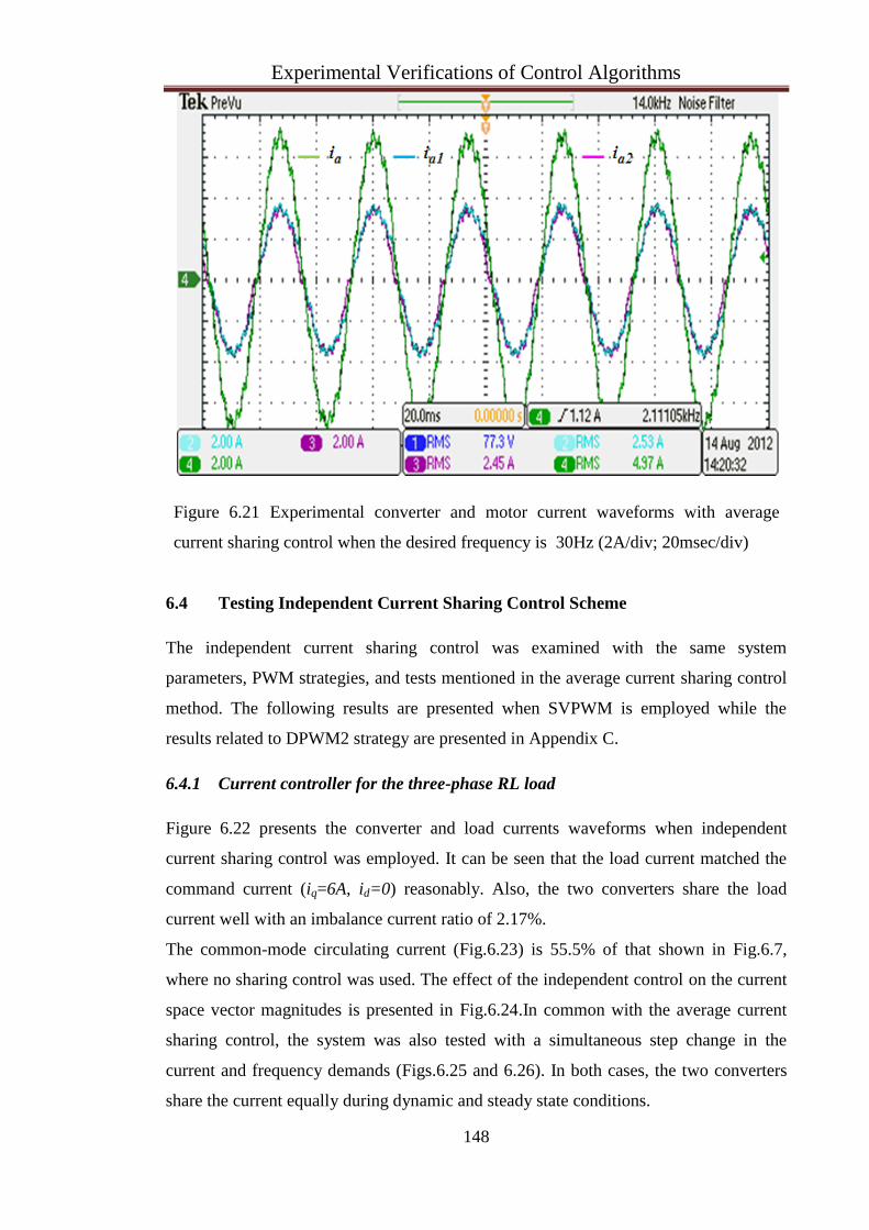
Experimental Verifications of Control Algorithms
148
Figure 6.21 Experimental converter and motor current waveforms with average
current sharing control when the desired frequency is 30Hz (2A/div; 20msec/div)
6.4 Testing Independent Current Sharing Control Scheme
The independent current sharing control was examined with the same system
parameters, PWM strategies, and tests mentioned in the average current sharing control
method. The following results are presented when SVPWM is employed while the
results related to DPWM2 strategy are presented in Appendix C.
6.4.1 Current controller for the three-phase RL load
Figure 6.22 presents the converter and load currents waveforms when independent
current sharing control was employed. It can be seen that the load current matched the
command current (iq=6A, id=0) reasonably. Also, the two converters share the load
current well with an imbalance current ratio of 2.17%.
The common-mode circulating current (Fig.6.23) is 55.5% of that shown in Fig.6.7,
where no sharing control was used. The effect of the independent control on the current
space vector magnitudes is presented in Fig.6.24.In common with the average current
sharing control, the system was also tested with a simultaneous step change in the
current and frequency demands (Figs.6.25 and 6.26). In both cases, the two converters
share the current equally during dynamic and steady state conditions.

Experimental Verifications of Control Algorithms
149
Figure 6.22 Experimental converter and load current waveforms with independent
current sharing control when the desired frequency is 50Hz (2A/div; 10msec/div)
Figure 6.23 Experimental common mode circulating current with independent sharing
control at 50Hz
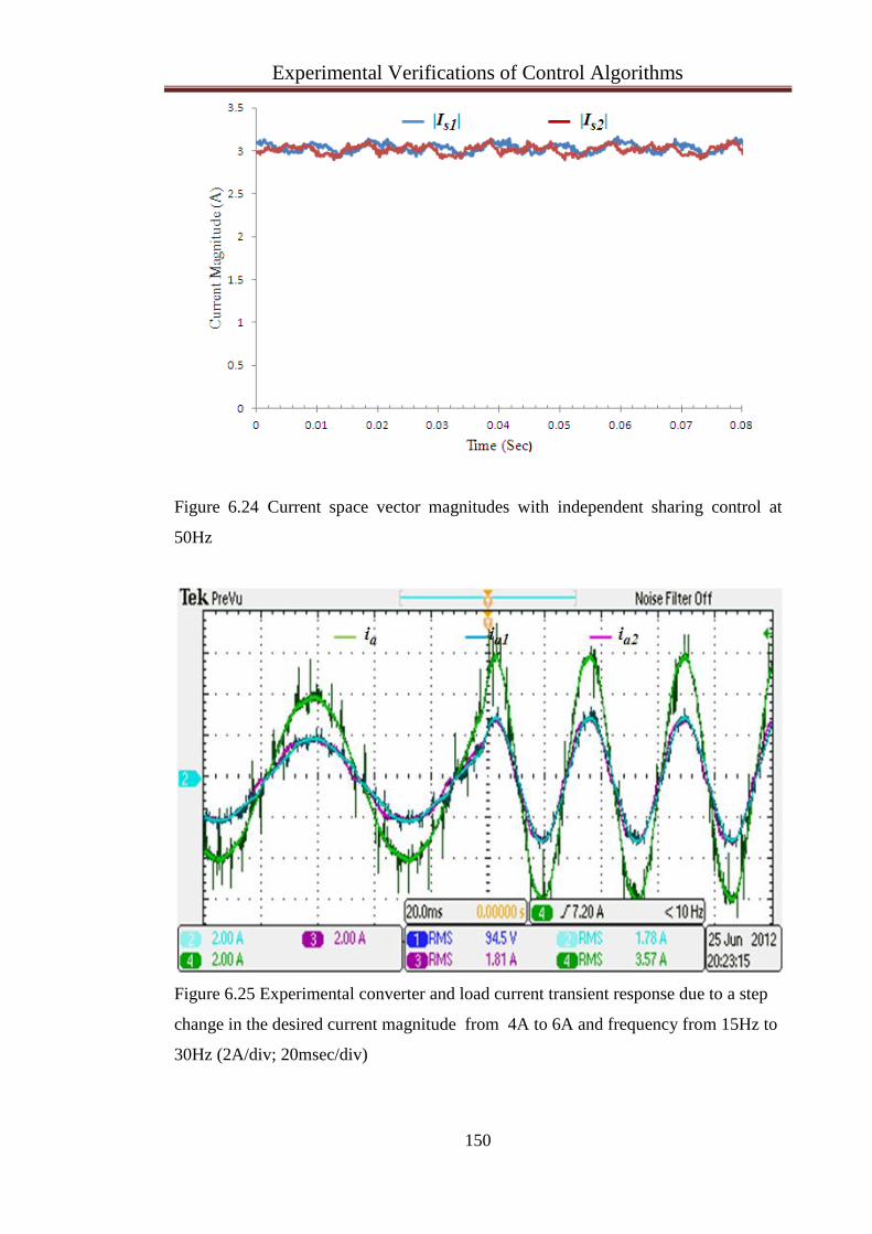
Experimental Verifications of Control Algorithms
150
Figure 6.24 Current space vector magnitudes with independent sharing control at
50Hz
Figure 6.25 Experimental converter and load current transient response due to a step
change in the desired current magnitude from 4A to 6A and frequency from 15Hz to
30Hz (2A/div; 20msec/div)

Experimental Verifications of Control Algorithms
151
Figure 6.26 Experimental converter and load current transient response due to a step
change in the desired current magnitude from 4A to 6A and frequency from 25Hz to
50Hz (2A/div; 20msec/div)
More results can be found in Appendix C, where the current waveforms are collected
using the LabViewTM
panel.
6.4.2 Open loop V/f control for the three-phase induction motor
Figures.6.27 to 6.29 show the results for the open loop V/f speed control for the three-
phase induction motor. The independent current sharing control was examined with
different desired frequencies. The independent current sharing control showed an
excellent current sharing capability regardless of the differences in the current sharing
reactors and the dead time for the two converters.

Experimental Verifications of Control Algorithms
152
Figure 6.27 Experimental converter and motor current waveforms with independent
current sharing control when the desired frequency is 50Hz (2A/div; 20msec/div)
Figure 6.28 Experimental converter and motor current waveforms with independent
current sharing control when the desired frequency is 20Hz (2A/div; 20msec/div)

Experimental Verifications of Control Algorithms
153
Figure 6.29 Experimental converter and motor current waveforms with independent
current sharing control when the desired frequency is 30Hz (2A/div; 10msec/div)
6.5 Testing of Impedance Emulation Current Sharing Control Scheme
The impedance emulation current sharing control was investigated with the same
system parameters, PWM strategy, and tests mentioned in the previous methods. The
following results are presented when the SVPWM strategy is employed.
6.5.1 Current controller for the three-phase RL load
Figure 6.30 demonstrates the current distribution between the parallel-connected
converters with the impedance emulation current sharing control. The two converters
shared the load current with a current imbalance ratio equal to 2.87%.
Further examinations of the control are achieved through subjecting the system to a
simultaneous step change in the desired frequency and quadrature axis load current.
Figures 6.31 and 6.32 explore the transient response when the demand frequency is
changed from 25Hz to 50Hz and from 15Hz to 30Hz respectively. The desired q-axis
load current was stepped from 4A to 6A in both cases. It can be seen that good transient
response is obtained in terms of current distribution regardless of the sudden variation in
the desired frequency and load current.

Experimental Verifications of Control Algorithms
154
Figure 6.30 Experimental converter and load current waveforms with resistance
emulation current sharing control when the desired frequency is 50Hz (2A/div;
10msec/div)
Figure 6.31 Transient response due to a step change in load current and frequency
from 25Hz to 50Hz (2A/div; 20msec/div)
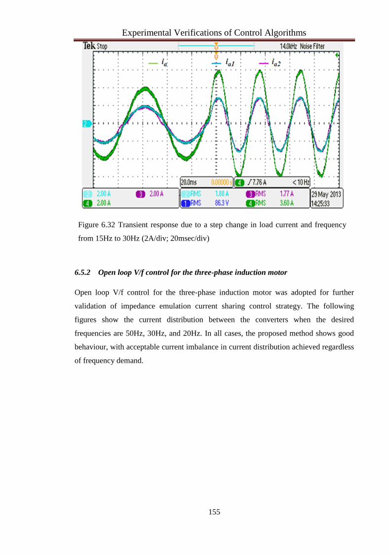
Experimental Verifications of Control Algorithms
155
Figure 6.32 Transient response due to a step change in load current and frequency
from 15Hz to 30Hz (2A/div; 20msec/div)
6.5.2 Open loop V/f control for the three-phase induction motor
Open loop V/f control for the three-phase induction motor was adopted for further
validation of impedance emulation current sharing control strategy. The following
figures show the current distribution between the converters when the desired
frequencies are 50Hz, 30Hz, and 20Hz. In all cases, the proposed method shows good
behaviour, with acceptable current imbalance in current distribution achieved regardless
of frequency demand.

Experimental Verifications of Control Algorithms
156
Figure 6.33 Experimental converter and motor current waveforms with sharing
control when the desired frequency is 50Hz (2A/div; 10msec/div)
Figure 6.34 Experimental converter and motor current waveforms with sharing
control when the desired frequency is 30Hz (2A/div; 10msec/div)
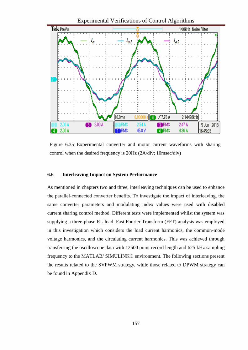
Experimental Verifications of Control Algorithms
157
Figure 6.35 Experimental converter and motor current waveforms with sharing
control when the desired frequency is 20Hz (2A/div; 10msec/div)
6.6 Interleaving Impact on System Performance
As mentioned in chapters two and three, interleaving techniques can be used to enhance
the parallel-connected converter benefits. To investigate the impact of interleaving, the
same converter parameters and modulating index values were used with disabled
current sharing control method. Different tests were implemented whilst the system was
supplying a three-phase RL load. Fast Fourier Transform (FFT) analysis was employed
in this investigation which considers the load current harmonics, the common-mode
voltage harmonics, and the circulating current harmonics. This was achieved through
transferring the oscilloscope data with 12500 point record length and 625 kHz sampling
frequency to the MATLAB/ SIMULINK® environment. The following sections present
the results related to the SVPWM strategy, while those related to DPWM strategy can
be found in Appendix D.

Experimental Verifications of Control Algorithms
158
6.6.1 Combined current
For non-interleaved converters, the harmonic spectrum of the load current (ia) is shown
in Fig.6.36. It can be seen that the harmonic components are concentrated around the
integer multiples of the switching frequency which is 6 kHz.
When symmetric interleaving is adopted, the harmonics around the odd multiples of the
carrier frequency are almost eliminated (see Fig.6.37). Contrary to natural sampled
PWM, complete harmonic cancellation usually did not occur since regular sampled
PWM was employed [53] [52]. It can be seen that the THD of the current is strongly
influenced since its value is 73% of that of un-interleaved converters.
This test was repeated for a low modulation index value using SVPWM and for high
and low values of modulation index using the DPWM2 strategy. The THD reduction is
summarized in Table 6.1, where the THD is assumed unity for non-interleaved
converters.
Figure 6.36 Experimental combined output current spectra for non-interleaved
converters using SVPWM at M=0.9

Experimental Verifications of Control Algorithms
159
Figure 6.37 Experimental combined output current spectra for symmetrically
interleaved converters using SVPWM at M=0.9
Modulation index THD reduction for
SVPWM
THD reduction for
DPWM2
0.5 14.4% 40%
0.9 26.7% 39.9%
Table 6.1 Experimental THD for different modulation index values and PWM
strategies
It is obvious that the harmonic cancellation for the DPWM is significantly higher than
for SVPWM when low modulation index values are used. This is because when
SVPWM is used, the harmonic energy concentrates around twice the switching
frequency at low modulation index values and around the switching frequency at high
modulation index values. Conversely, with DPWM, the harmonic energy always
concentrates around the switching frequency.

Experimental Verifications of Control Algorithms
160
6.6.2 Inter-module circulating current
As explained in previous chapters, interleaving converts some of the harmonic
components to a low and high frequency circulating current. Unfortunately, the high
frequency circulating current is not mitigated by active current sharing control methods.
Therefore, additional inter-module reactors will be necessary to limit the high frequency
circulating current. This effect can be demonstrated through monitoring the circulating
current harmonic spectra for non-interleaved converters (see Fig.6.38) and for
symmetrically interleaved converters, as in Fig.6.39. It can be seen that a considerable
circulating current between the converters has been excited due to symmetrical
interleaving. The circulating current harmonic components are dominated around the
switching frequency and its odd integer multiples. This circulating current increases the
RMS and peak values of the converter current which may lead to inductor saturation.
However, the DPWM strategy shows a lower peak current value when interleaving is
adopted and accordingly the possibility of inductor saturation is reduced. The reason
behind this is because of the IGBTs clamping periods when the current in its maximum
positive or maximum negative periods.
Figure 6.38 Experimental circulating current spectra for non-interleaved converters
using SVPWM at M=0.9

Experimental Verifications of Control Algorithms
161
Figure 6.39 Experimental circulating current spectra for symmetrically interleaved
converters using SVPWM at M=0.9
6.6.3 Common-mode voltage
Figure 6.40 and 6.41 compare the common-mode voltage spectra for non-interleaved
and interleaved converters. The voltage harmonic magnitudes are normalised to the DC
link voltage. In the case of non-interleaved converters, there are harmonics centred
around the switching frequency and its integer multiples. The harmonics around the odd
multiples of the carrier frequency were eliminated when symmetrical interleaving was
adopted with the two parallel-connected converters. Accordingly, in motor drive
applications, this harmonic elimination will reduce the possibility of bearing failure and
electromagnetic interference noise that causes nuisance trips in the inverter drive [102]
[103] [113].
The observations of the combined current, the circulating current, and the common-
mode voltage confirm the simulation results noted in chapter four.
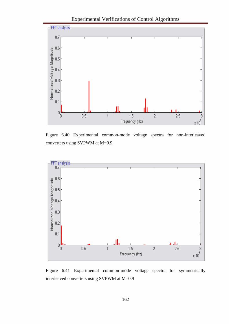
Experimental Verifications of Control Algorithms
162
Figure 6.40 Experimental common-mode voltage spectra for non-interleaved
converters using SVPWM at M=0.9
Figure 6.41 Experimental common-mode voltage spectra for symmetrically
interleaved converters using SVPWM at M=0.9

Experimental Verifications of Control Algorithms
163
6.7 Summary
In this chapter, the algorithms of the SVPWM and DPWM strategies were tested with
one AC/DC/AC converter, which is connected to a three-phase RL load. The three-
phase modulating signal waveforms were presented. Also, for the DPWM strategy, the
IGBT clamping periods during the maximum positive and maximum negative load
current were clarified.
The proposed current sharing control methods for the parallel-connected AC/DC/AC
converters were tested using different PWM strategies (SVPWM & DPWM) and
different applications. These applications were current control for three-phase R-L loads
and open loop V/f control for a three-phase induction motor. Further investigations were
conducted into these methods through subjecting the system to a wide range of variation
in the desired frequency and current. These investigations demonstrated the current
distributions between the two converters during transient and steady state conditions.
The results showed that the proposed control methods resumed the equal current sharing
between the paralleled converters regardless of the differences in their physical
parameters. .Table 6.2 compares the simulated and experimental results in terms of
current distribution between the parallel-connected converters, when different current
sharing control schemes are adopted. When the current sharing control schemes are
deactivated, the simulated and experimental current imbalance ratios are 56% and 38%
respectively.
Current sharing control
scheme
Imbalance current ratio
Simulated Experimental
Average current sharing
control
1.17% 3.34%
Independent current
sharing control
0.27% 2.17%
Impedance emulation
current sharing control
2.29% 2.8%
Table 6.2 Simulated and experimental current imbalance ration for SVPWM strategy
Finally, experimental measurements have been used to demonstrate the effects of
interleaving on paralleled-connected three-phase PWM converters. These measurements
included the combined current, the common-mode voltage, and the circulating current

Experimental Verifications of Control Algorithms
164
between the paralleled converters. FFT analysis showed significant improvements in the
load current and the common-mode voltage through adopting interleaving techniques in
parallel-connected converters. Nevertheless, this technique produced additional low and
high frequency circulating currents. Consequently, additional passive components
became necessary to limit high frequency circulating current. Simulated and
experimental results for the combined output current THD for different PWM strategies
are presented in Table 6.3. The improvement in the common-mode voltage due to
symmetrical interleaving is presented in Table 6.4. The magnitude of the dominant
harmonic component at the switching frequency (6 kHz) is presented as a percentage of
the DC link voltage and for different PWM strategies.
Modulation
index
Combined output current THD reduction
SVPWM DPWM2
Simulated Experimental Simulated Experimental
0.5 31.5% 14.4% 49.6% 40%
0.9 30% 26.7% 35.46% 39.9%
Table 6. 3 Simulated and experimental combined output current THD for different
modulation index values and PWM strategies
Modulation
index
Normalised common-mode voltage magnitude of the 6 kHz harmonic
component
SVPWM DPWM2
Simulated Experimental Simulated Experimental
λ=0 λ=180 λ=0 λ=180 λ=0 λ=180 λ=0 λ=180
0.5 0.54 0.0004 0.54 0.0005 0.35 0.012 0.34 0.068
0.9 0.292 0.0002 0.295 0.012 0.267 0.003 0.26 0.011
Table 6.4 Simulated and experimental common-mode voltage magnitude of the 6 kHz
harmonic component.
It can be seen that the simulated and experimental results are well matched, the above
tables point out that the DPWM strategy is the strategy of choice when symmetrical
interleaving is adopted for parallel-connected converters.

Experimental Verifications of Control Algorithms
165
The Performances for the proposed methods are summarised in Table 6.5.These
performances include, the algorithm simplicity, expandability, cost, dependency on the
PWM strategy and limitations of each method.
Current sharing method Features
Time sharing No current sharing reactors
Communication between converters is not
required.
Circulating current control is not necessary.
Limited to a low number of parallel-connected
converters.
The converters should be physically very closed
Average current sharing
control
Current sharing reactors are used
Only one piece of information is shared between
the parallel connected converters
Easily extended to any number of parallel
connected converters
Applied regardless the PWM strategy
Separate zero axis circulating current control is
not required
Only one PI controller is used by each unit
Independent current
sharing control
Current sharing reactors are required.
No information is shared between converters
Easily extended to any number of parallel
connected converters
Applied regardless the PWM strategy
Separate zero axis circulating current control is
not required
Only one PI controller is used by each unit
LPF is used in the control loop which slow down
the dynamic response
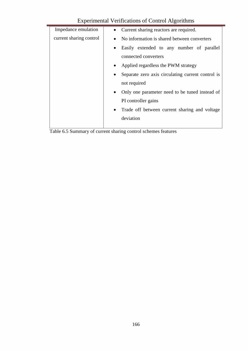
Experimental Verifications of Control Algorithms
166
Impedance emulation
current sharing control
Current sharing reactors are required.
No information is shared between converters
Easily extended to any number of parallel
connected converters
Applied regardless the PWM strategy
Separate zero axis circulating current control is
not required
Only one parameter need to be tuned instead of
PI controller gains
Trade off between current sharing and voltage
deviation
Table 6.5 Summary of current sharing control schemes features

Conclusions and Future Work
167
Chapter 7. Conclusions and Future Work
7.1 Conclusions
This thesis has discussed active current sharing control methods for three-phase
parallel-connected AC/DC/AC converters with a separate but non-isolated DC link.
Two applications have been investigated, a current controller for three-phase RL load,
and open loop V/f speed control for a three-phase induction motor. Detailed
experimental work has been conducted and the results obtained have been used to verify
the proposed methods.
Four current sharing control methods have been suggested where the main objective is
to achieve equal current sharing between equally rated parallel-connected converters.
These methods are, a time sharing approach, average current sharing control,
independent current sharing control and impedance emulation current sharing control.
Conventional SVPWM and DPWM strategies have been used to assess the capability of
each method in maintaining equal current distribution between the two converters. This
assessment has been carried out over a wide range of output frequencies during both
transient and steady state conditions.
In the time sharing approach, the operating time is divided between the converters.
Accordingly, the current sharing reactors become redundant, leading to a small size and
a lower cost for the system. Furthermore, low switching losses permit a smaller heat
sink. The root-mean-square (RMS) value of the switching device current rating is also
decreased. However, this method is only recommended for a low number of parallel
units since the IGBT switches must be able to handle the peak load current. Also, the
paralleled converters should be physically much closed with a reduced cable inductance
which will limit the dv/dt and the system EMI
In contrast to previous work, average current sharing control strategy was applied by
considering the current space vector magnitude instead of the three-phase current in a
stationary or rotating reference frame representation. Accordingly, only one PI
compensator was used, as only one piece of information needs to be shared between the
parallel-connected converters. Therefore, both considerable algorithm simplification
and trouble-free extendibility to any number of units is achieved.
Conclusions and Future Work
168
In the third proposed method, an independent modular current sharing controller is
proposed to produce equal current sharing between equally rated converters. Each
converter uses only local information to obtain the desired current value. The converter
currents are represented by the current space vector magnitude. For this reason, only
one PI compensator is used to modify the modulation index of each converter in such a
way that circulating current mitigation is ensured. Separate zero axis current control is
not necessary to achieve equal current sharing between the converters, thus reducing the
computational burden necessary for the implementation of the control algorithm. In
addition, the proposed method may be easily extended to three or more converter
modules.
In the final approach, the current distribution is improved through impedance emulation
instead of physical impedance on the output of each converter. The impedance value is
proportional to the converter current space vector magnitude, i.e. a large emulated
impedance is used when the converter shared current is large and vice versa. The
control algorithm is simple and modular since each converter is controlled
independently of the other converters. Nevertheless, this approach suffers from a steady
state error in terms of current distribution between the converters and the voltage drop
on the virtual impedance.
It has been demonstrated that the proposed methods works properly during transient and
steady state and with both the SVPWM and DPWM strategy. However, the DPWM
strategy is only preferred in applications in which high modulation index values are
used.
The impact of symmetric interleaving on the performance of parallel connected
converters has been assessed. The output current, common-mode voltage, and
circulating current were all considered. It has been verified that interleaving improves
the output current and common-mode voltage performances, but an increase in
circulating current is the corresponding penalty.
To examine the proposed control algorithms before the system implementation, current
sharing analysis and MATLAB/ SIMULINK® models have been developed and
explained in detail. Then, the control algorithms were implemented in real-time on one
DSP microcontroller based on a detailed hardware design procedure. The experimental
results were a close match with the simulation results.

Conclusions and Future Work
169
7.2 Future work
There are several research tasks for future work in this area. Some of these are stated
below:
To achieve a truly modular structure, it is preferred to redesign the parallel
connected converters, such that each converter has its own microcontroller.
Accordingly, a carrier and modulating signal synchronisation process will be
necessary
Further improvements can be made by adopting an interleaved parallel converter
structure with a common DC link instead of separate DC links. This structure
will lead to DC link current harmonic cancellation and for that reason the DC
link capacitor size will be reduced. Also, only one DC link voltage sensor will
be required and the control algorithm becomes simpler when the DC link
voltage is controlled
To improve the input current harmonic performance, it is recommended to use a
PWM rectifier instead of a diode rectifier. The circulating current in the inverter
side is independent on the circulating current of the rectifier side. Consequently,
the proposed current sharing control method could be used on both input and
output sides
The DPWM scheme has 50% switching losses reduction when compared with
conventional SVM. Also, the DPWM current and voltage harmonics are
decreased considerably compared to the conventional SVM level for a high
modulation index. It is therefore recommended that a hybrid PWM scheme be
used, where a conventional SVM strategy is adopted for a low modulation index
and DPWM strategy for a high modulation index
It would be interesting to investigate the operation of parallel-connected
converters with a three-phase current sharing reactor instead of three single
phase current sharing reactors
It is suggested to use a multivariable PI based dq current regulator which
provides superior axes decoupling compared to conventional synchronous frame
dq current regulator used in the current research [112]

References
170
References
[1] C. Keller and Y. Tadros, "Are paralleled IGBT modules or paralleled IGBT
inverters the better choice?," in Power Electronics and Applications, 1993., Fifth
European Conference on, 1993, pp. 1-6 vol.5.
[2] X. Kun, F. C. Lee, D. Borojevic, Y. Zhihong, and S. Mazumder, "Interleaved
PWM with discontinuous space-vector modulation," IEEE Transactions on
Power Electronics, vol. 14, pp. 906-917, 1999.
[3] Z. Di, F. Wang, R. Burgos, L. Rixin, and D. Boroyevich, "Impact of Interleaving
on AC Passive Components of Paralleled Three-Phase Voltage-Source
Converters," IEEE Transactions on Industry Applications, vol. 46, pp. 1042-
1054, 2010.
[4] D. J. Shortt, W. T. Michael, R. L. Avant, and R. E. Palma, "A 600-W Four-Stage
Phase-Shifted-Parallel DC-to-DC Converter," IEEE Transactions on Power
Electronics, vol. PE-2, pp. 101-108, 1987.
[5] R. H. Wu, T. Kohama, Y. Kodera, T. Ninomiya, and F. Ihara, "Load-current-
sharing control for parallel operation of DC-to-DC converters," in Power
Electronics Specialists Conference, 1993. PESC '93 Record., 24th Annual IEEE,
1993, pp. 101-107.
[6] Y. Zhihong, D. Boroyevich, C. Jae-Young, and F. C. Lee, "Control of
circulating current in two parallel three-phase boost rectifiers," IEEE
Transactions on Power Electronics,, vol. 17, pp. 609-615, 2002.
[7] J. Birk and B. Andresen, "Parallel-connected converters for optimizing
efficiency, reliability and grid harmonics in a wind turbine," in Power
Electronics and Applications, 2007 European Conference on, 2007, pp. 1-7.
[8] X. Zhuang, L. Rui, Z. Hui, X. Dianguo, and C. C. H. Zhang, "Control of Parallel
Multiple Converters for Direct-Drive Permanent-Magnet Wind Power
Generation Systems," IEEE Transactions on Power Electronics, vol. 27, pp.
1259-1270.
[9] W. Chunxue, L. Jianlin, Z. Xiaoguang, and X. Honghua, "Research on
Circulation of Parallel Three-Phase Converters in MW Wind Power System," in

References
171
Power Electronics and Intelligent Transportation System, 2008. PEITS '08.
Workshop on, 2008, pp. 349-354.
[10] J. Janning and A. Schwery, "Next generation variable speed pump-storage
power stations," in Power Electronics and Applications, 2009. EPE '09. 13th
European Conference on, 2009, pp. 1-10.
[11] A. Bocquel and J. Janning, "Analysis of a 300 MW variable speed drive for
pump-storage plant applications," in Power Electronics and Applications, 2005
European Conference on, 2005, pp. 10 pp.-P.10.
[12] L. Asimmoaei, E. Aeloiza, J. H. Kim, P. Enjeti, F. Blaabjerg, L. T. Moran, and S.
K. Sul, "An interleaved active power filter with reduced size of passive
components," in Applied Power Electronics Conference and Exposition, 2006.
APEC '06. Twenty-First Annual IEEE, 2006, p. 8 pp.
[13] J. Suo, Y. Yang, and C. Qi, "Control of circulating current for direct parallel
grid-connected inverters in photovoltaic power generation," in Mechatronics and
Automation, 2009. ICMA 2009. International Conference on, 2009, pp. 3805-
3810.
[14] WeiYu, X. Dehong, and Z. Chaoyang, "Parallel control of the UPS inverters," in
Applied Power Electronics Conference and Exposition, 2008. APEC 2008.
Twenty-Third Annual IEEE, 2008, pp. 939-944.
[15] Y. B. Byun, T. G. Koo, K. Y. Joe, E. S. Kim, J. I. Seo, and D. H. Kim, "Parallel
operation of three-phase UPS inverters by wireless load sharing control," in
Telecommunications Energy Conference, 2000. INTELEC. Twenty-second
International, 2000, pp. 526-532.
[16] C. Hui, Z. Rongxiang, and Y. Huan, "Study on Ideal Operation Status of Parallel
Inverters," IEEE Transactions on Power Electronics,, vol. 23, pp. 2964-2969,
2008.
[17] J. M. Guerrero, L. Hang, and J. Uceda, "Control of Distributed Uninterruptible
Power Supply Systems," IEEE Transactions on Industrial Electronics, vol. 55,
pp. 2845-2859, 2008.
[18] K. Lee, T. M. Jahns, G. Venkataramanan, and W. E. Berkopec, "DC-Bus
Electrolytic Capacitor Stress in Adjustable-Speed Drives Under Input Voltage
Unbalance and Sag Conditions," IEEE Transactions on Industry Applications.,
vol. 43, pp. 495-504, 2007.
References
172
[19] C.Fortescue, "Method of symmetrical coordinates to the solution of polyphase
network," Trans. AIEE, vol. 37, pp. 1027-1140, 1918.
[20] T. Itkonen, J. Luukko, T. Laakkonen, P. Silventoinen, and O. Pyrhonen,
"Switching effects in directly paralleled three-phase AC/DC/AC converters with
separate DC links," in Power Electronics Specialists Conference, 2008. PESC
2008. IEEE, 2008, pp. 1937-1943.
[21] M. H. Rashid, "POWER ELECTRONICS HANDBOOK:DEVICES, CIRCUITS,
AND APPLICATIONS," 3rd ed. ed: Elsevier Inc., 2011.
[22] A. K. Ali Emadi, Zhong Nie "Integrated Power Electronic Converters and
Digital Control," CRC Press, 2009.
[23] T. A. L. D. Grahame Holmes, "Pulse Width Modulation for Power Converters:
Principles and Practice," IEEE Press, 2003.
[24] L. Z. William Shepherd "Power Converter Circuits," Marcel Dekker, 2004.
[25] N. Mohan, "Power Electronics: A First Course," John Wiley & Sons, 2012.
[26] H. W. van der Broeck, H. C. Skudelny, and G. V. Stanke, "Analysis and
realization of a pulsewidth modulator based on voltage space vectors," IEEE
Transactions on Industry Applications, vol. 24, pp. 142-150, 1988.
[27] J. F. Moynihan, M. G. Egan, and J. M. D. Murphy, "Theoretical spectra of
space-vector-modulated waveforms," IEE Proceedings -Electric Power
Applications, vol. 145, pp. 17-24, 1998.
[28] J. W. Kolar, H. Ertl, and F. C. Zach, "Influence of the modulation method on the
conduction and switching losses of a PWM converter system," IEEE
Transactions on Industry Applications, vol. 27, pp. 1063-1075, 1991.
[29] D. C. Rus, N. S. Preda, I. I. Incze, M. Imecs, Szabo, x, and C., "Comparative
analysis of PWM techniques: Simulation and DSP implementation," in IEEE
International Conference on Automation Quality and Testing Robotics (AQTR),
2010 pp. 1-6.
[30] C. Tsung-Po, L. Yen-Shin, and L. Chang-Huan, "A new space vector
modulation technique for inverter control," in Power Electronics Specialists
Conference, 1999. PESC 99. 30th Annual IEEE, 1999, pp. 777-782 vol.2.
[31] A. M. Hava, R. J. Kerkman, and T. A. Lipo, "A high-performance generalized
discontinuous PWM algorithm," Industry Applications, IEEE Transactions on,
vol. 34, pp. 1059-1071, 1998.
References
173
[32] A. M. Hava, R. J. Kerkman, and T. A. Lipo, "Simple analytical and graphical
methods for carrier-based PWM-VSI drives," IEEE Transactions on Power
Electronics, vol. 14, pp. 49-61, 1999.
[33] W. Yunxiang, M. A. Shafi, A. M. Knight, and R. A. McMahon, "Comparison of
the Effects of Continuous and Discontinuous PWM Schemes on Power Losses
of Voltage-Sourced Inverters for Induction Motor Drives," IEEE Transactions
on Power Electronics, vol. 26, pp. 182-191.
[34] W. Xiao-ling and Y. Xiang-gen, "The Unified PWM Implementation Method for
Three-Phase Inverters," in IEEE International Conference in Electric Machines
& Drives , 2007. IEMDC '07. , 2007, pp. 241-246.
[35] T. P. Chen, "Circulating zero-sequence current control of parallel three-phase
inverters," IEE Proceedings - Electric Power Applications, vol. 153, pp. 282-
288, 2006.
[36] M. P. Kazmierkowski and L. Malesani, "Current control techniques for three-
phase voltage-source PWM converters: a survey," IEEE Transactions on
Industrial Electronics, vol. 45, pp. 691-703, 1998.
[37] D. M. Brod and D. W. Novotny, "Current Control of VSI-PWM Inverters,"
IEEE Transactions on Industry Applications, vol. IA-21, pp. 562-570, 1985.
[38] M. Mohseni and S. M. Islam, "A New Vector-Based Hysteresis Current Control
Scheme for Three-Phase PWM Voltage-Source Inverters," IEEE Transactions
on Power Electronics, , vol. 25, pp. 2299-2309, 2010.
[39] H. Nagase, Y. Matsuda, K. Ohnishi, H. Ninomiya, and T. Koike, "High-
Performance Induction Motor Drive System Using a PWM Inverter," IEEE
Transactions on Industry Applications, vol. IA-20, pp. 1482-1489, 1984.
[40] D. N. Zmood and D. G. Holmes, "Stationary frame current regulation of PWM
inverters with zero steady-state error," IEEE Transactions on Power Electronics,
vol. 18, pp. 814-822, 2003.
[41] D. G. Holmes, B. P. McGrath, and S. G. Parker, "Current Regulation Strategies
for Vector-Controlled Induction Motor Drives," IEEE Transactions on
Industrial Electronics, vol. 59, pp. 3680-3689.
[42] T. M. Rowan and R. J. Kerkman, "A New Synchronous Current Regulator and
an Analysis of Current-Regulated PWM Inverters," IEEE Transactions on
Industry Applications, vol. IA-22, pp. 678-690, 1986.

References
174
[43] P. M. Simone Buso "Digital Control in Power Electronics," Morgan & Claypool,
2006.
[44] Q. Yao and D. G. Holmes, "A simple, novel method for variable-hysteresis-band
current control of a three phase inverter with constant switching frequency," in
Industry Applications Society Annual Meeting, 1993., Conference Record of the
1993 IEEE, 1993, pp. 1122-1129 vol.2.
[45] D. O. Neacsu, "Power Switching Converters," Taylor & Francis, 2006.
[46] U. N. Arendt Wintrich, Werner Tursky, Tobias Reimann, "Application Manual
Power Semiconductors," 2011.
[47] Z. Di, F. Wang, R. Burgos, L. Rixin, and D. Boroyevich, "Interleaving Impact
on AC Passive Components of Paralleled Three-Phase Voltage-Source
Converters," in Industry Applications Society Annual Meeting, 2008. IAS '08.
IEEE, 2008, pp. 1-7.
[48] P. Ching-Tsai, C. Jui-Yang, L. Ching-Ming, J. Yu-Ling, and L. Yi-Hung,
"Modeling of circulating currents for grid-connected parallel three-phase
inverters," in SICE Annual Conference, 2008, 2008, pp. 1319-1322.
[49] W. Tongzhen, L. Yaohua, H. Gang, and Z. Haibin, "Modeling and control of
circulating current in parallel three-phase PWM converters," in Power
Electronics and Drive Systems, 2003. PEDS 2003. The Fifth International
Conference on, 2003, pp. 910-914 Vol.2.
[50] P. Ching-Tsai and L. Yi-Hung, "Modeling and Coordinate Control of
Circulating Currents in Parallel Three-Phase Boost Rectifiers," IEEE
Transactions on Industrial Electronics, vol. 54, pp. 825-838, 2007.
[51] C. Casablanca and S. Jian, "Interleaving and Harmonic Cancellation Effects in
Modular Three-Phase Voltage-Sourced Converters," in IEEE Workshops on
Computers in Power Electronics, 2006. COMPEL '06. , 2006, pp. 275-281.
[52] Z. Di, W. Fei, R. Burgos, and D. Boroyevich, "Common-Mode Circulating
Current Control of Paralleled Interleaved Three-Phase Two-Level Voltage-
Source Converters With Discontinuous Space-Vector Modulation," IEEE
Transactions on Power Electronics, vol. 26, pp. 3925-3935, 2011.
[53] T. Beechner and S. Jian, "Harmonic cancellation under interleaved PWM with
harmonic injection," in Power Electronics Specialists Conference, 2008. PESC
2008. IEEE, 2008, pp. 1515-1521.

References
175
[54] S. K. T. Miller, T. Beechner, and S. Jian, "A Comprehensive Study of Harmonic
Cancellation Effects in Interleaved Three-Phase VSCs," in Power Electronics
Specialists Conference, 2007. PESC 2007. IEEE, 2007, pp. 29-35.
[55] T. Kawabata and S. Higashino, "Parallel operation of voltage source inverters,"
IEEE Transactions on Industry Applications, vol. 24, pp. 281-287, 1988.
[56] Y. Komatsuzaki, "Cross current control for parallel operating three phase
inverter," in Power Electronics Specialists Conference, PESC '94 Record., 25th
Annual IEEE, 1994, pp. 943-950 vol.2.
[57] Y. Ito and O. Iyama, "Parallel redundant operation of UPS with robust current
minor loop," in Power Conversion Conference - Nagaoka 1997., Proceedings of
the, 1997, pp. 489-494 vol.1.
[58] C. S. Lee, S. Kim, C. B. Kim, S. C. Hong, J. S. Yoo, S. W. Kim, C. H. Kim, S.
H. Woo, and S. Y. Sun, "Parallel UPS with a instantaneous current sharing
control," in Industrial Electronics Society, 1998. IECON '98. Proceedings of the
24th Annual Conference of the IEEE, 1998, pp. 568-573 vol.1.
[59] J. Holtz, W. Lotzkat, and K. H. Werner, "A high-power multitransistor-inverter
uninterruptable power supply system," IEEE Transactions on Power Electronics,
vol. 3, pp. 278-285, 1988.
[60] L. H. Walker, "10-MW GTO converter for battery peaking service," IEEE
Transactions on Industry Applications, vol. 26, pp. 63-72, 1990.
[61] K. Imaie, S. Ito, and S. Ueda, "PWM control method of multiple inverters for
Maglev," in Power Conversion Conference, 1993. Yokohama 1993., Conference
Record of the, 1993, pp. 55-60.
[62] S. Ito, K. Imaie, K. Nakata, S. Ueda, and K. Nakamura, "A series of PWM
methods of a multiple inverter for adjustable frequency drive," in Power
Electronics and Applications, 1993., Fifth European Conference on, 1993, pp.
190-195 vol.4.
[63] S. Ogasawara, J. Takagaki, H. Akagi, and A. Nabae, "A novel control scheme of
a parallel current-controlled PWM inverter," IEEE Transactions on Industry
Applications, vol. 28, pp. 1023-1030, 1992.
[64] K. Kamiyama, T. Ohmae, and T. Sukegawa, "Application trends in AC motor
drives," in Industrial Electronics, Control, Instrumentation, and Automation,
1992. Power Electronics and Motion Control., Proceedings of the 1992
International Conference on, 1992, pp. 31-36 vol.1.

References
176
[65] K. Matsui, Y. Murai, M. Watanabe, M. Kaneko, and F. Ueda, "A pulsewidth-
modulated inverter with parallel connected transistors using current-sharing
reactors," IEEE Transactions on Power Electronics, vol. 8, pp. 186-191, 1993.
[66] F. Ueda, K. Matsui, M. Asao, and K. Tsuboi, "Parallel-connections of
pulsewidth modulated inverters using current sharing reactors," IEEE
Transactions on Power Electronics, vol. 10, pp. 673-679, 1995.
[67] S. Bin and G. Venkataramanan, "Parallel operation of voltage source inverters
with minimal intermodule reactors," in Industry Applications Conference, 2004.
39th IAS Annual Meeting. Conference Record of the 2004 IEEE, 2004, p. 162.
[68] R. Pollanen, A. Tarkiainen, M. Niemela, and J. Pyrhonen, "Control of zero-
sequence current in parallel connected voltage source PWM rectifiers using
converter-flux-based control," in Power Electronics and Applications, 2005
European Conference on, 2005, pp. 10 pp.-P.10.
[69] F. Xunbo, E. Chunliang, L. Jianlin, and X. Honghua, "Modeling and simulation
of parallel-operation grid-connected inverter," in Industrial Technology, 2008.
ICIT 2008. IEEE International Conference on, 2008, pp. 1-6.
[70] Z. Yu and J. Zhenhua, "Sliding mode based zero-sequence current mitigation of
parallel-connected power converters," in Electric Machines and Drives
Conference, 2009. IEMDC '09. IEEE International, 2009, pp. 1658-1663.
[71] X. Zhuang, L. Rui, Z. Hui, X. Dianguo, and C. C. H. Zhang, "Control of Parallel
Multiple Converters for Direct-Drive Permanent-Magnet Wind Power
Generation Systems," IEEE Transactions on Power Electronics, vol. 27, pp.
1259-1270, 2012.
[72] T. Itkonen, J. Luukko, and R. Pollanen, "Analysis of current characteristics of
parallel three-phase voltage source inverters," in Power Electronics and
Applications, 2009. EPE '09. 13th European Conference on, 2009, pp. 1-10.
[73] D. Fingas and P. W. Lehn, "Operation of parallel three-phase converters as a
motor drive," in Industrial Electronics, 2009. IECON '09. 35th Annual
Conference of IEEE, 2009, pp. 1217-1222.
[74] C. Tsung-Po, "Common-Mode Ripple Current Estimator for Parallel Three-
Phase Inverters," IEEE Transactions on Power Electronics, vol. 24, pp. 1330-
1339, 2009.
[75] X. Zhuang, L. Rui, Z. Hui, X. Dianguo, and C. C. H. Zhang, "Control of Parallel
Multiple Converters for Direct-Drive Permanent-Magnet Wind Power

References
177
Generation Systems," IEEE Transactions on Power Electronics, vol. 27, pp.
1259-1270.
[76] C. Tsung-Po, "Dual-Modulator Compensation Technique for Parallel Inverters
Using Space-Vector Modulation," IEEE Transactions on Industrial Electronics
vol. 56, pp. 3004-3012, 2009.
[77] A. Kelly, K. Rinne, and E. O'Malley, "Masterless multirate control of parallel
DC-DC converters," in Applied Power Electronics Conference and Exposition
(APEC), 2010 Twenty-Fifth Annual IEEE, pp. 2189-2193.
[78] P. Ching-Tsai and L. Yi-Hung, "Modeling and Control of Circulating Currents
for Parallel Three-Phase Boost Rectifiers With Different Load Sharing," IEEE
Transactions on Industrial Electronics, vol. 55, pp. 2776-2785, 2008.
[79] Z. Di, F. Wang, R. Burgos, L. Rixin, T. Thacker, and D. Boroyevich,
"Interleaving impact on harmonic current in DC and AC passive components of
paralleled three-phase voltage-source converters," in Applied Power Electronics
Conference and Exposition, 2008. APEC 2008. Twenty-Third Annual IEEE,
2008, pp. 219-225.
[80] Z. Di, W. Fei, R. Burgos, and D. Boroyevich, "Total Flux Minimization Control
for Integrated Inter-Phase Inductors in Paralleled, Interleaved Three-Phase Two-
Level Voltage-Source Converters With Discontinuous Space-Vector
Modulation," IEEE Transactions on Power Electronics, vol. 27, pp. 1679-1688,
2012.
[81] H. Chung-Chuan and C. Po-Tai, "A Multicarrier Pulse Width Modulator for the
Auxiliary Converter and the Diode Rectifier," IEEE Transactions on Power
Electronics, vol. 26, pp. 1119-1126, 2011.
[82] H. Chung-Chuan, "A Multicarrier PWM for Parallel Three-Phase Active Front-
End Converters," IEEE Transactions on Power Electronics, vol. 28, pp. 2753-
2759, 2013.
[83] L. Asiminoaei, E. Aeloiza, P. N. Enjeti, and F. Blaabjerg, "Shunt Active-Power-
Filter Topology Based on Parallel Interleaved Inverters," IEEE Transactions on
Industrial Electronics, vol. 55, pp. 1175-1189, 2008.
[84] D. O. Neacsu, E. Wagner, and B. S. Borowy, "A Simulation Benchmark for
Selection of the PWM Algorithms for Three-Phase Interleaved Converters,"
IEEE Transactions on Industrial Electronics, vol. 55, pp. 1628-1636, 2008.

References
178
[85] L. Chang-Shiarn and C. Chern-Lin, "Single-wire current-share paralleling of
current-mode-controlled DC power supplies," IEEE Transactions on Industrial
Electronics, vol. 47, pp. 780-786, 2000.
[86] S. Xiao, L. Yim-Shu, and X. Dehong, "Modeling, analysis, and implementation
of parallel multi-inverter systems with instantaneous average-current-sharing
scheme," IEEE Transactions on Power Electronics vol. 18, pp. 844-856, 2003.
[87] H. Ming, H. Haibing, X. Yan, and H. Zhongyi, "Distributed Control for AC
Motor Drive Inverters in Parallel Operation," IEEE Transactions on Industrial
Electronics, vol. 58, pp. 5361-5370, 2011.
[88] Z. Yu, D. Shanxu, K. Yong, and C. Jian, "The Restrain of Harmonic Circulating
Currents between Parallel Inverters," in Power Electronics and Motion Control
Conference, 2006. IPEMC 2006. CES/IEEE 5th International, 2006, pp. 1-5.
[89] D. G. Holmes, T. A. Lipo, B. P. McGrath, and W. Y. Kong, "Optimized Design
of Stationary Frame Three Phase AC Current Regulators," IEEE Transactions
on Power Electronics, vol. 24, pp. 2417-2426, 2009.
[90] D. J. P. G. F. Franklin, and M. L. Workman, "Digital Control of Dynamic
response," 3rd ed: T. Hyde, S. Feinstein, and R. Tonomura, Eds. Addison
Wesley Longman Inc., 1998.
[91] D. J. P. G. F. Franklin, and M. L. Workman, "Digital Control of Dynamic
Systems," 3rd ed: T. Hyde, S. Feinstein, and R. Tonomura, Eds. Addison
Wesley Longman Inc., 1997.
[92] B. A. Shenoi, "Introduction to digital signal processing and filter design," New
Jersey: John Wiley & Son, Inc., 2006.
[93] S. Winder, "Analogue and digital filter design book," Elsevier, 2002.
[94] X. Shungang and X. Jianping, "Parallel control strategy of single-phase inverter
based on virtual impedance," in Communications, Circuits and Systems
(ICCCAS), 2010 International Conference on, pp. 589-592.
[95] Z. Yu, Y. Mi, L. Fangrui, and K. Yong, "Instantaneous Current-Sharing Control
Strategy for Parallel Operation of UPS Modules Using Virtual Impedance,"
IEEE Transactions on Power Electronics, vol. 28, pp. 432-440, 2013.
[96] R. H. B. Richard C. Dorf, "Modern Control Systems," 9th Edition ed: Prentice
Hall 2001.
[97] L. Baohua, M. Miao, L. Weiguo, and L. Guangzhao, "Simulation and
experiment study of space vector pulse width modulation," in ICEMI '09. 9th
References
179
International Conference on Electronic Measurement & Instruments, 2009,
2009, pp. 1-408-1-412.
[98] H. W. V. D. Broeck, "Analysis of harmonics in voltage fed inverter drives
caused by PWM schemes with discontinuous switching operation," in European
Power Electronics Conference, 1991, pp. 261-266.
[99] G. Liping, "Implementation of digital PID controllers for DC-DC converters
using digital signal processors," in Electro/Information Technology, 2007 IEEE
International Conference on, 2007, pp. 306-311.
[100] L. Corradini, W. Stefanutti, and P. Mattavelli, "Analysis of Multisampled
Current Control for Active Filters," IEEE Transactions on Industry Applications,
vol. 44, pp. 1785-1794, 2008.
[101] A. Munoz-Garcia, T. A. Lipo, and D. W. Novotny, "A new induction motor V/f
control method capable of high-performance regulation at low speeds," IEEE
Transactions on Industry Applications, vol. 34, pp. 813-821, 1998.
[102] A. M. Hava and E. Un, "Performance Analysis of Reduced Common-Mode
Voltage PWM Methods and Comparison With Standard PWM Methods for
Three-Phase Voltage-Source Inverters," IEEE Transactions on Power
Electronics, vol. 24, pp. 241-252, 2009.
[103] M. J. Duran, J. A. Riveros, F. Barrero, H. Guzman, and J. Prieto, "Reduction of
Common-Mode Voltage in Five-Phase Induction Motor Drives Using Predictive
Control Techniques," IEEE Transactions on Industry Applications vol. 48, pp.
2059-2067, 2012.
[104] A. M. Hava, U. Ayhan, and V. V. Aban, "A DC bus capacitor design method for
various inverter applications," in Energy Conversion Congress and Exposition
(ECCE), 2012 IEEE, pp. 4592-4599.
[105] U. Ayhan and A. M. Hava, "Analysis and characterization of DC Bus ripple
current of two-level inverters using the equivalent centered harmonic approach,"
in Energy Conversion Congress and Exposition (ECCE), 2011 IEEE, 2011, pp.
3830-3837.
[106] J. W. Kolar, T. M. Wolbank, and M. Schrodl, "Analytical calculation of the
RMS current stress on the DC link capacitor of voltage DC link PWM converter
systems," in Electrical Machines and Drives, 1999. Ninth International
Conference on (Conf. Publ. No. 468), 1999, pp. 81-89.

References
180
[107] J. W. Kolar and S. D. Round, "Analytical calculation of the RMS current stress
on the DC-link capacitor of voltage-PWM converter systems," IEE Proceedings
- Electric Power Applications, vol. 153, pp. 535-543, 2006.
[108] F. Sargos, "IGBT Power Electronics Teaching System Principle for sizing power
converters ", Application Note 2008.
[109] A. Technologies, "2.0 Amp Gate Drive Optocoupler with Integrated (VCE)
Desaturation Detection and Fault Status Feedback," Technical Data 2005.
[110] D. spectrum, "ezdspF28335 Technical Refernce," 2007.
[111] "TMS320F28335, TMS320F28334, TMS320F28332, TMS320F28235,
TMS320F28234, TMS320F28232, Digital Signal Controller (DSCs)," Texas
Instrument, Tech. Rep. March 2010.
[112] B. Bahrani, S. Kenzelmann, and A. Rufer, "Multivariable-PI-Based dq Current
Control of Voltage Source Converters With Superior Axis Decoupling
Capability," IEEE Transactions on Idustrail Electronics, vol. 58, pp. 3016-3026,
2011.
[113] T. P. Chen, "Circulating zero-sequence current control of parallel three-phase
inverters," Electric Power Applications, IEE Proceedings -, vol. 153, pp. 282-
288, 2006.

Appendix A
181
Appendix A
A.1 Parallel Converters Wiring Diagrams
Figure A.1 Schematic of parallel-connected converters-Wiring diagram

Appendix A
182
Figure A.2 Schematic of the first AC/DC/AC converter
Figure A.3 Schematic of the second AC/DC/AC converter

Appendix A
183
Figure A.4 Schematic of 3-phase rely card.
Figure A.5 Schematic of converter current sensor circuit

Appendix A
184
Figure A.6 Schematic of converter voltage sensor circuit
Figure A.7 Schematic of load current sensor circuit
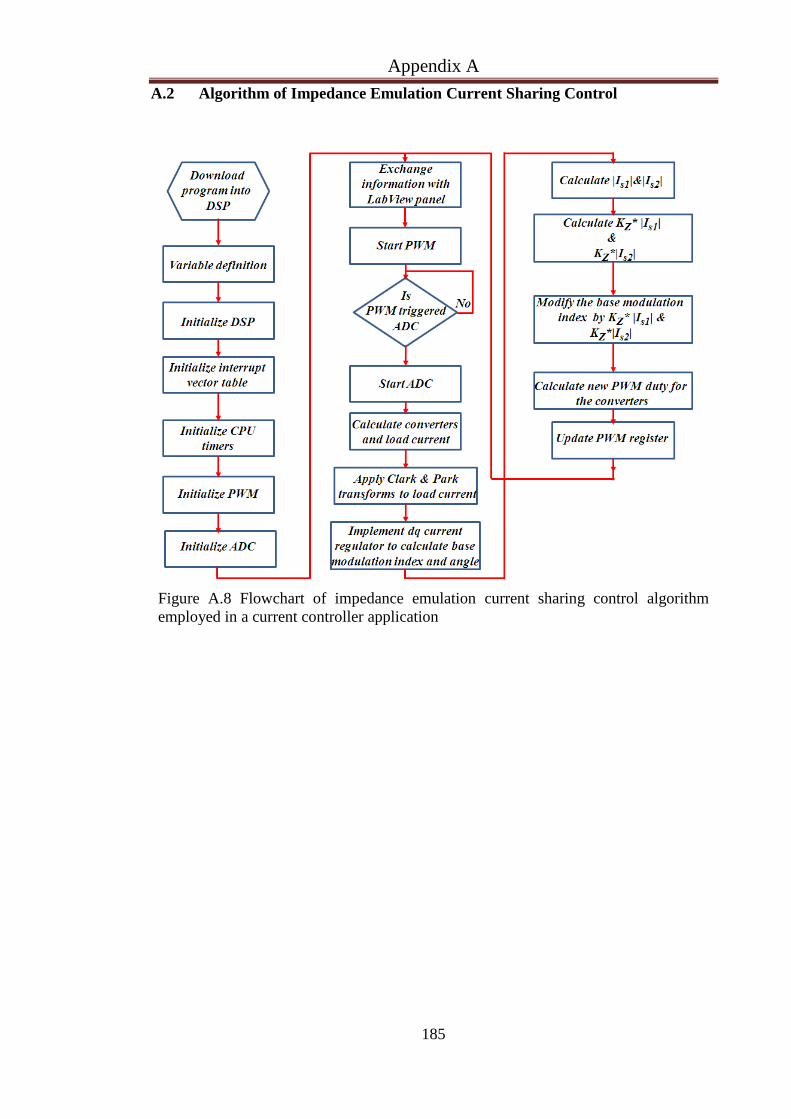
Appendix A
185
A.2 Algorithm of Impedance Emulation Current Sharing Control
Figure A.8 Flowchart of impedance emulation current sharing control algorithm
employed in a current controller application
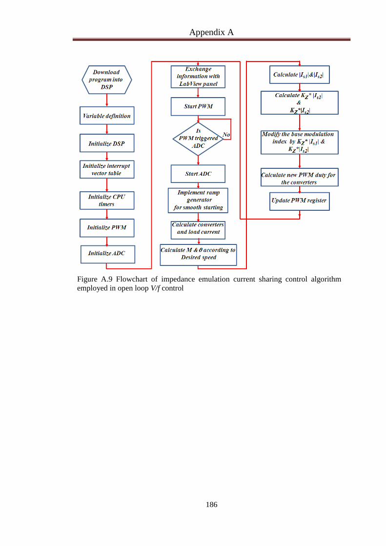
Appendix A
186
Figure A.9 Flowchart of impedance emulation current sharing control algorithm
employed in open loop V/f control

Appendix B
Appendix B. Simulation Results
B.1 Interleaving Impacts on System Performance When DPWM2 is Adopted
B.1.1 Combined current
Figure B.1 Combined current spectra for non-interleaved converters using DPWM2 at
M=0.9
Figure B.2 Combined current spectra for non-interleaved converters using DPWM2 at
M=0.5

Appendix B
188
Figure B.3 Combined current spectra for symmetrically interleaved converters using
DPWM2 at M=0.9
Figure B.4 Combined current spectra for symmetrically interleaved converters using
DPWM2 at M=0.5

Appendix B
189
B.1.2 Circulating current
Figure B.5 Circulating current spectra for interleaved converters using DPWM2 at
M=0.9
Figure B.6 Circulating current spectra for interleaved converters using DPWM2 at
M=0.5

Appendix B
190
B.1.3 Common mode voltage
Figure B.7 Spectra of common-mode voltage for non-interleaved converters with
DPWM2 at M=0.9
Figure B.8 Spectra of common-mode voltage for non-interleaved converters with
DPWM2 at M=0.5

Appendix B
191
Figure B.9 Spectra of common-mode voltage for symmetrically interleaved
converters with DPWM2 at M=0.9
Figure B.10 Spectra of common-mode voltage for symmetrically interleaved
converters with DPWM2 at M=0.5

Appendix C
Appendix C. SVPWM Strategy Experimental Results
C.1 Testing Average Current Sharing Control
C.1.1 Current controller for three-phase RL load
Figure C.1 Experimental converter and load current waveforms without sharing
control
Figure C.2 Experimental converter and load current waveforms with average current
sharing control at 50Hz

Appendix C
Figure C.3 Experimental current space vector magnitude transient response due to a
step change in the desired current magnitude and frequency from 15Hz to 30Hz
Figure C.4 Experimental converter and load current transient response due to a step
change in the desired current magnitude and frequency from 15Hz to 30Hz

Appendix C
Figure C.5 Experimental converter and load current transient response due to a step
change in the desired current magnitude and frequency from 25Hz to 50Hz
Figure C.6 Experimental converter and load current waveforms with average current
sharing control at 10Hz
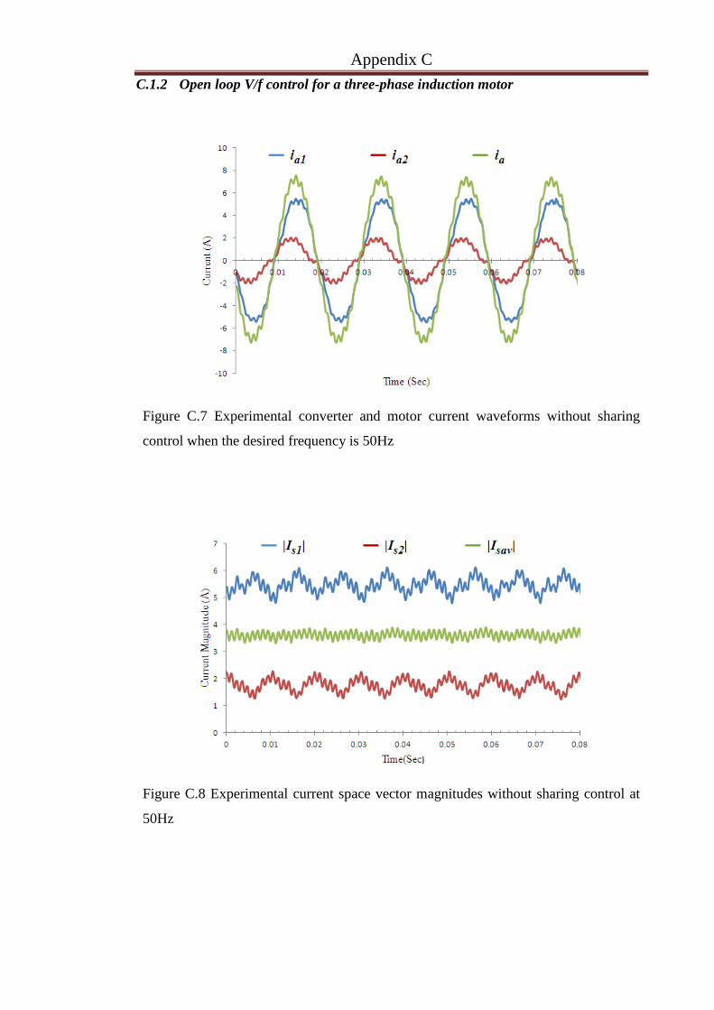
Appendix C
C.1.2 Open loop V/f control for a three-phase induction motor
Figure C.7 Experimental converter and motor current waveforms without sharing
control when the desired frequency is 50Hz
Figure C.8 Experimental current space vector magnitudes without sharing control at
50Hz

Appendix C
Figure C.9 Experimental converter and motor current waveforms with average
Figure C.10 Experimental current space vector magnitudes with average current
sharing control at 50Hz
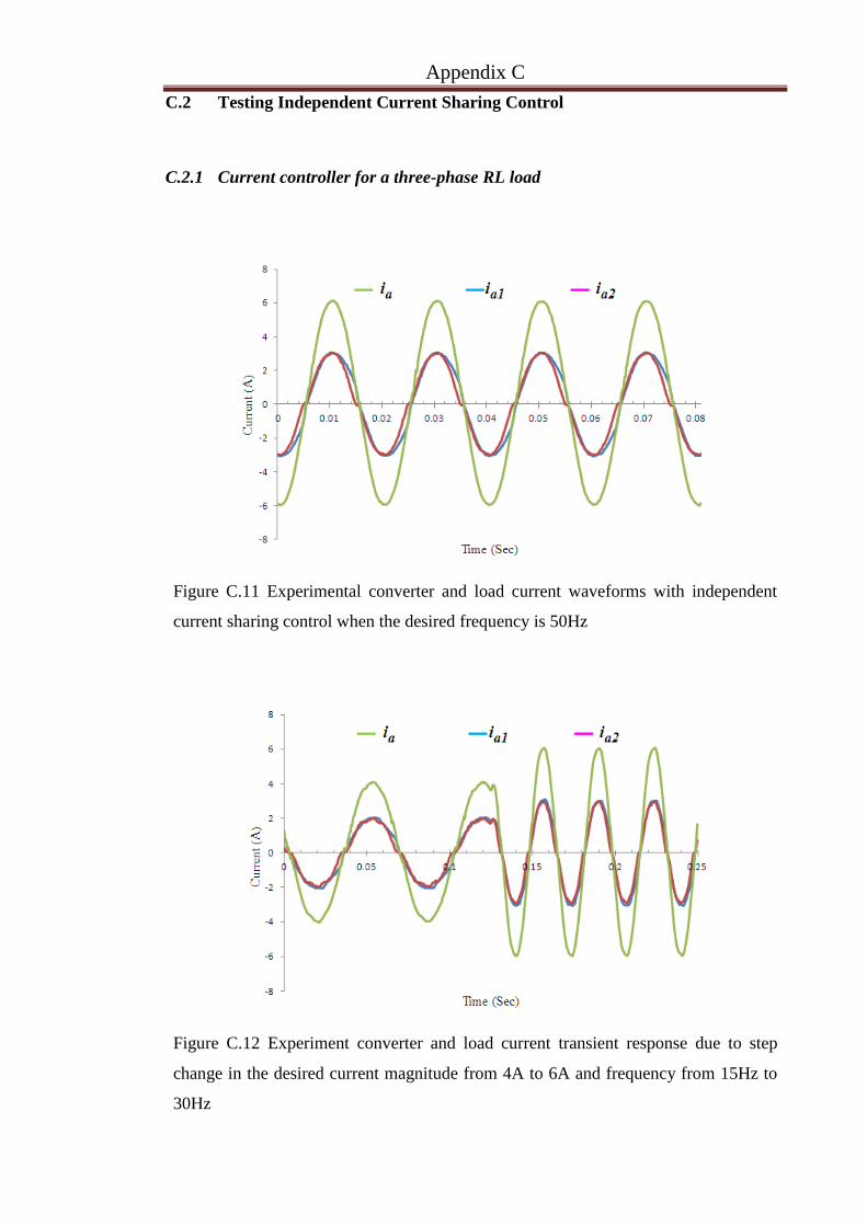
Appendix C
C.2 Testing Independent Current Sharing Control
C.2.1 Current controller for a three-phase RL load
Figure C.11 Experimental converter and load current waveforms with independent
current sharing control when the desired frequency is 50Hz
Figure C.12 Experiment converter and load current transient response due to step
change in the desired current magnitude from 4A to 6A and frequency from 15Hz to
30Hz

Appendix C
198
Figure C.13 Experimental current space vector magnitude transient response due to a
step change in the desired current magnitude and frequency from 15Hz to 30Hz
Figure C.14 Experiment converters and load current transient response due to a step
change in the desired current magnitude from 4A to 6A and frequency from 25Hz to
50Hz

Appendix C
199
C.3 Testing Impedance Current Sharing Control
C.3.1 Current controller for a three-phase RL load
Figure C.15 Experimental converter and load current waveforms with impedance
emulation current sharing control when the desired frequency is 50Hz
Figure C.16 Experiment converters and load current transient response due to a step
change in the desired current magnitude from 4A to 6A and frequency from 25Hz to
50Hz

Appendix C
200
Figure C.17 Experiment converters and load current transient response due to a step
change in the desired current magnitude from 4A to 6A and frequency from 15Hz to
30Hz
C.4 Interleaving Impacts on System Performance
C.4.1 Combined current
Figure C.18 Experimental combined current spectra for non-interleaved converters
using SVPWM at M=0.5

Appendix C
201
Figure C.19 Experimental combined current spectra for symmetrically interleaved
converters using SVPWM at M=0.5
C.4.2 Inter-module circulating current
Figure C.20 Experimental circulating current spectra for non-interleaved converters
using SVPWM at M=0.5

Appendix C
202
Figure C.21 Experimental circulating current spectra for symmetrically interleaved
converters using SVPWM at M=0.5
C.4.3 Common-mode voltage
Figure C.22 Experimental common-mode voltage spectra for non-interleaved
converters using SVPWM at M=0.5
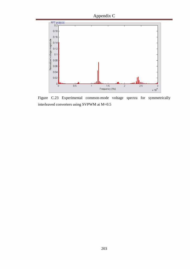
Appendix C
203
Figure C.23 Experimental common-mode voltage spectra for symmetrically
interleaved converters using SVPWM at M=0.5
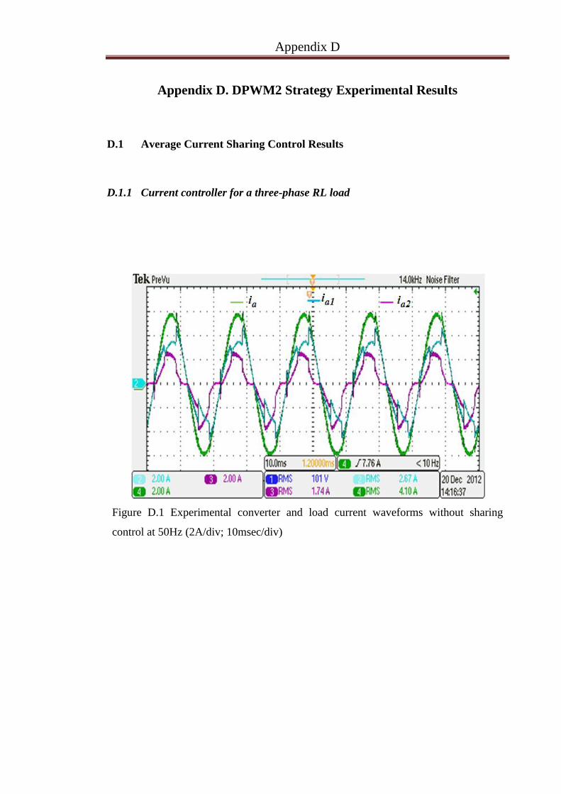
Appendix D
Appendix D. DPWM2 Strategy Experimental Results
D.1 Average Current Sharing Control Results
D.1.1 Current controller for a three-phase RL load
Figure D.1 Experimental converter and load current waveforms without sharing
control at 50Hz (2A/div; 10msec/div)

Appendix D
205
Figure D.2 Experimental common-mode circulating current without sharing control
Figure D.3 Experimental converter and load current waveforms with average current
sharing control at 50Hz (2A/div; 10msec/div)
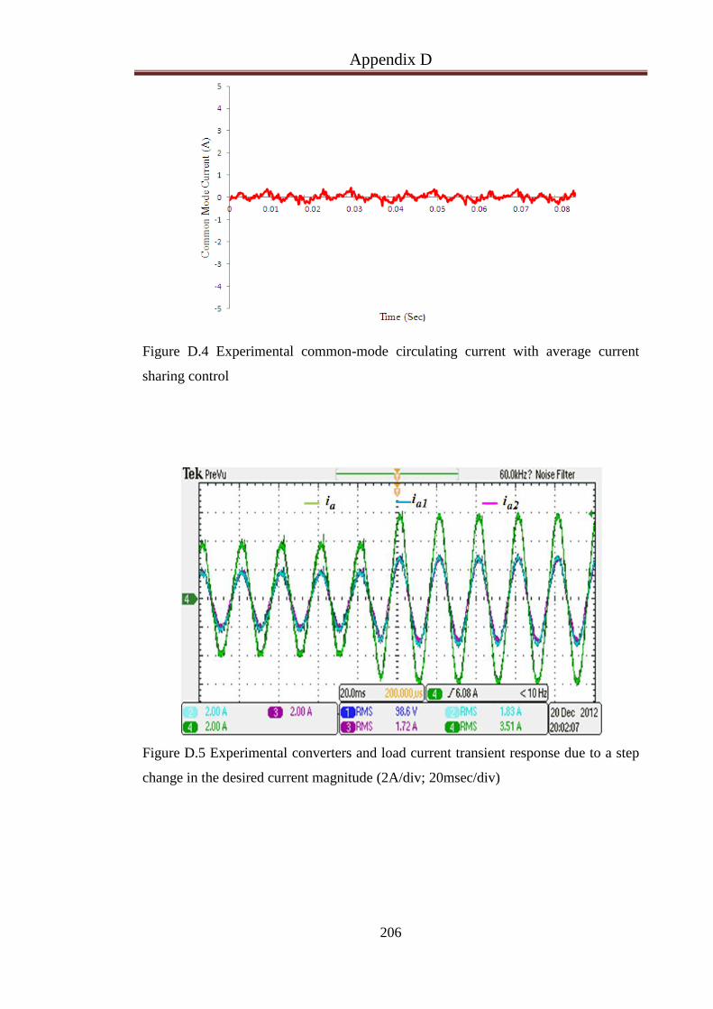
Appendix D
206
Figure D.4 Experimental common-mode circulating current with average current
sharing control
Figure D.5 Experimental converters and load current transient response due to a step
change in the desired current magnitude (2A/div; 20msec/div)

Appendix D
207
D.2 Independent Current Sharing Control Results
D.2.1 Current controller for a three-phase RL load
Figure D.6 Experimental converter and load current waveforms with independent
current sharing control at 50Hz (2A/div; 10msec/div)
Figure D.7 Experimental common mode circulating current with independent sharing
control at 50Hz

Appendix D
208
Figure D.8 Experiment converters and load current transient response due to a step
change in the desired current magnitude (2A/div; 20msec/div)
D.3 Interleaving Impacts on System Performance
D.3.1 Combined current
Figure D.9 Experimental combined current spectra for non-interleaved converters
using DPWM2 at M=0.9

Appendix D
209
Figure D.10 Experimental combined current spectra for non-interleaved converters
using DPWM2 at M=0.5
Figure D.11 Experimental combined current spectra for symmetrically interleaved
converters using DPWM2 at M=0.9

Appendix D
210
Figure D.12 Experimental combined current spectra for symmetrically interleaved
converters using DPWM2 at M=0.5
D.3.2 Inter-module circulating current
Figure D.13 Experimental circulating current spectra for non-interleaved converters
using DPWM2 at M=0.9

Appendix D
211
Figure D.14 Experimental circulating current spectra for non-interleaved converters
using DPWM2 at M=0.5
Figure D.15 Experimental circulating current spectra for symmetrically interleaved
converters using DPWM2 at M=0.9

Appendix D
212
Figure D.16 Experimental circulating current spectra for symmetrically interleaved
converters using DPWM2 at M=0.5
D.3.3 Common-mode voltage
Figure D.17 Experimental common-mode voltage spectra for non-interleaved
converters using DPWM2 at M=0.9
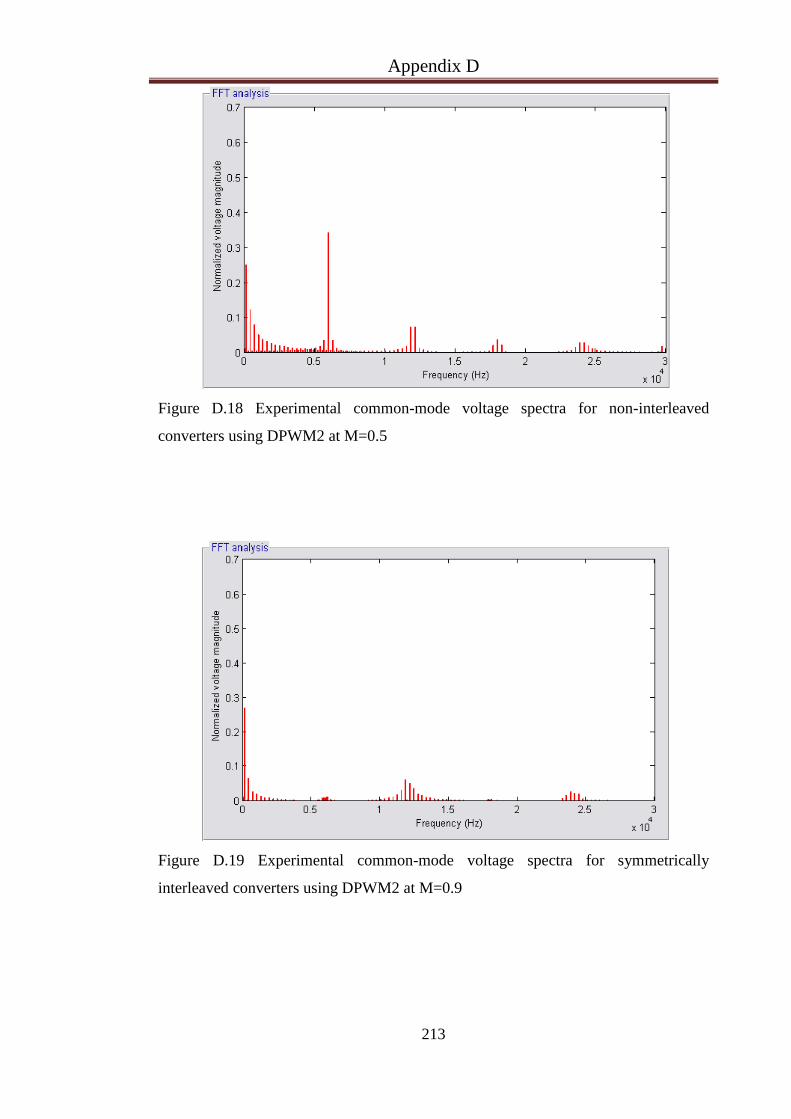
Appendix D
213
Figure D.18 Experimental common-mode voltage spectra for non-interleaved
converters using DPWM2 at M=0.5
Figure D.19 Experimental common-mode voltage spectra for symmetrically
interleaved converters using DPWM2 at M=0.9

Appendix D
214
Figure D.20 Experimental common-mode voltage spectra for symmetrically
interleaved converters using DPWM2 at M=0.5