Embed Size (px)
Citation preview

Actel Quick Start Guide
Libero IDE v8.0

Table of Contents
2 Actel Quick Start Guide Libero IDE v8.0
Actel Corporation, Mountain View, CA 94043© 2007 Actel Corporation. All rights reserved.
Printed in the United States of America
Part Number: 5-02-9123-13
Release: June 2007
No part of this document may be copied or reproduced in any form or by any means without prior written consent of Actel.Actel makes no warranties with respect to this documentation and disclaims any implied warranties of merchantability or fitness for a particular purpose. Information in this document is subject to change without notice. Actel assumes no responsibility for any errors that may appear in this document.This document contains confidential proprietary information that is not to be disclosed to any unauthorized person without prior written consent of Actel Corporation.
TrademarksActel and the Actel logotype are registered trademarks of Actel Corporation.
Adobe and Acrobat Reader are registered trademarks of Adobe Systems, Inc.
Mentor Graphics, Precision RTL, Exemplar Spectrum, and Leonoardo Spectrum are registered trademarks of Mentor Graphics, Inc.
WaveFormerLite is a registered trademark of SynaptiCAD, Inc.
Synplify is a registered trademark of Synplicity, Inc.
Sun and Sun Workstation, SunOS, and Solaris are trademarks or registered trademarks of Sun Microsystems, Inc
Synopsys is a registered trademark of Synopsys, Inc.
Verilog is a registered trademark of Open Verilog International.
Viewlogic, ViewSim, ViewDraw and SpeedWave are trademarks or registered trademarks of Viewlogic Systems, Inc.
Windows is a registered trademark and Windows NT is a trademark of Microsoft Corporation in the U.S. and other countries.
UNIX is a registered trademark of X/Open Company Limited.
All other products or brand names mentioned are trademarks or registered trademarks of their respective holders.
Table of Contents
Introduction . . . . . . . . . . . . . . . . . . . . . . . . . . . . . . 5Document Organization . . . . . . . . . . . . . . . . . . . . . . . . . . . . . . 5
Document Assumptions . . . . . . . . . . . . . . . . . . . . . . . . . . . . . . 5
Document Conventions . . . . . . . . . . . . . . . . . . . . . . . . . . . . . . 6
Your Comments . . . . . . . . . . . . . . . . . . . . . . . . . . . . . . . . . . 6
Online Help . . . . . . . . . . . . . . . . . . . . . . . . . . . . . . . . . . . . 6
Actel Manuals . . . . . . . . . . . . . . . . . . . . . . . . . . . . . . . . . . . 6
1 Libero IDE Overview . . . . . . . . . . . . . . . . . . . . . . . . . 7Libero IDE Family Support . . . . . . . . . . . . . . . . . . . . . . . . . . . . 7
SmartDesign in the Project Manager . . . . . . . . . . . . . . . . . . . . . . . . 9
Designer . . . . . . . . . . . . . . . . . . . . . . . . . . . . . . . . . . . . . . 9
Libero IDE Maintenance . . . . . . . . . . . . . . . . . . . . . . . . . . . . . 13
SDC and PDC Design Constraints in the Libero IDE . . . . . . . . . . . . . . 13
2 Actel Design Flows . . . . . . . . . . . . . . . . . . . . . . . . . 15Design Flow Illustrated . . . . . . . . . . . . . . . . . . . . . . . . . . . . . . . 15
Schematic-Based Design Flow Overview . . . . . . . . . . . . . . . . . . . . . 16
Schematic-Based Design Methodology . . . . . . . . . . . . . . . . . . . . . . 17
HDL Synthesis-Based Design Flow Overview . . . . . . . . . . . . . . . . . . . 18
HDL Synthesis-Based Design Methodology . . . . . . . . . . . . . . . . . . . 19
3 Quick Start Tutorial . . . . . . . . . . . . . . . . . . . . . . . . 21Design Flow . . . . . . . . . . . . . . . . . . . . . . . . . . . . . . . . . . . . 22
Step 1 – Open the Libero IDE Project in the Project Manager . . . . . . . . . . 22
Step 2 – Configuring the FlashROM . . . . . . . . . . . . . . . . . . . . . . . 23
Step 3 – Pre-Synthesis Simulation of the Design . . . . . . . . . . . . . . . . . 26
Step 4 – Synthesize the Design Using Synplicity . . . . . . . . . . . . . . . . . . 27
Step 5 – Specify Pin Constraints . . . . . . . . . . . . . . . . . . . . . . . . . . 28
Step 6 – Place-and-Route the Design . . . . . . . . . . . . . . . . . . . . . . . 28
Step 7 – Programming the A3P250 . . . . . . . . . . . . . . . . . . . . . . . . 30
4 Design Considerations . . . . . . . . . . . . . . . . . . . . . . . 31
Actel Quick Start Guide Libero IDE v8.0 3

Table of Contents
Naming Conventions . . . . . . . . . . . . . . . . . . . . . . . . . . . . . . . . 31
Hierarchical Designs . . . . . . . . . . . . . . . . . . . . . . . . . . . . . . . . 34
Multiple Sheet Designs . . . . . . . . . . . . . . . . . . . . . . . . . . . . . . . 34
Actel Libraries . . . . . . . . . . . . . . . . . . . . . . . . . . . . . . . . . . . 34
Adding Power and Ground . . . . . . . . . . . . . . . . . . . . . . . . . . . . . 34
Adding a Global Network . . . . . . . . . . . . . . . . . . . . . . . . . . . . . 35
Using ProASIC and ProASICPLUS Global Routing Resources . . . . . . . . . 37
Combinability . . . . . . . . . . . . . . . . . . . . . . . . . . . . . . . . . . . 38
Net Loading . . . . . . . . . . . . . . . . . . . . . . . . . . . . . . . . . . . . 45
Logic and I/O Utilization . . . . . . . . . . . . . . . . . . . . . . . . . . . . . 46
Adding Properties . . . . . . . . . . . . . . . . . . . . . . . . . . . . . . . . . 47
ALSPIN . . . . . . . . . . . . . . . . . . . . . . . . . . . . . . . . . . . . . . 50
Generating a Top-Level Symbol . . . . . . . . . . . . . . . . . . . . . . . . . . 55
Entering Constraints for Timing Driven Place-and-Route . . . . . . . . . . . . 55
Estimating Pre-Layout Timing . . . . . . . . . . . . . . . . . . . . . . . . . . 55
Adding Cores . . . . . . . . . . . . . . . . . . . . . . . . . . . . . . . . . . . . 56
A Product Support . . . . . . . . . . . . . . . . . . . . . . . . . . 57Customer Service . . . . . . . . . . . . . . . . . . . . . . . . . . . . . . . . . . 57
Actel Customer Technical Support Center . . . . . . . . . . . . . . . . . . . . . 57
Actel Technical Support . . . . . . . . . . . . . . . . . . . . . . . . . . . . . . 57
Website . . . . . . . . . . . . . . . . . . . . . . . . . . . . . . . . . . . . . . . 57
Contacting the Customer Technical Support Center . . . . . . . . . . . . . . . 58
Index . . . . . . . . . . . . . . . . . . . . . . . . . . . . . . . . 59
4 Actel Quick Start Guide Libero IDE v8.0
Introduction
The Actel Quick Start Guide for Libero IDE contains information for using the Libero IDE software to create designs for, and program, Actel devices.
This manual includes information about the Libero IDE software, which allows you to generate and/or import a netlist generated from a third-party CAE tool, perform pre-synthesis simulation, synthesize your design, place-and-route the design, run physical synthesis, perform static timing analysis, extract timing information, estimate power consumption, and generate a programming file to program an Actel FPGA.
This manual also refers to other Actel documents that contain additional information, including CAE software interface guides and simulation guides with specific information about using CAE tools with the Libero IDE.
Document OrganizationThe Actel Quick Start Guide for Libero is divided into the following chapters:
Chapter 1 - Libero IDE Overview gives an overview of the programs contained in the Designer software.
Chapter 2 - Actel Design Flows illustrates and describes the design flow for creating Actel designs using the Designer software and third-party CAE tools.
Chapter 3 - Quick Start Tutorial illustrates a basic VHDL design for the APA Evaluation Board targeted at the Actel ProASIC3E family.
Chapter 4 - Design Considerations contains useful information and procedures about creating designs using the Actel Designer software.
Appendix A - Product Support provides information about contacting Actel for customer and technical support.
Document Assumptions The information in this manual is based on the following assumptions:
1. You have installed the Libero IDE software.
2. You are familiar with PCs and Windows operating environments.
3. You are familiar with FPGA architecture and FPGA design software.
4. You are familiar with Libero IDE software and have prior experience with the ProASICPLUS family.
Actel Quick Start Guide Libero IDE v8.0 5

Introduction
Document ConventionsThe <act_fam> variable represents an Actel device family. To reference an actual family, substitute the name of the Actel device when you see this variable.
The <vhd_fam> variable represents Compiled VHDL libraries. To reference an actual compiled library, substitute the name of the library when you see this variable. Compiled VHDL libraries must begin with an alpha character.
Your CommentsActel Corporation strives to produce the highest quality online help and printed documentation. We want to help you learn about our products, so you can get your work done quickly. We welcome your feedback about this guide and our online help. Please send your comments to [email protected].
Online HelpOnline help specific to each software tool is available in the Libero IDE Project Manager, Designer, Silicon Explorer II, and Silicon Sculptor.
Actel ManualsLibero IDE includes printed and online manuals. The online manuals are in PDF format and available from Libero’s Start Menu and on the CD-ROM.
The complete list of Libero manuals is available on the Actel website at http://www.actel.com.
6 Actel Quick Start Guide Libero IDE v8.0

1Libero IDE Overview
Actel's Libero IDE offers the latest and best-in-class tools from leading EDA vendors such as Mentor Graphics, SynaptiCAD, Synplicity, and Magma Design Automation. These tools, combined with custom developed tools from Actel, are all integrated into a single FPGA development package. The Libero IDE flow includes a powerful Project Manager that guides you through the design process, keeps track of your design files, and manages file exchanges between the various tools. Libero IDE includes Actel's Designer software, which offers premier backend tools for physical implementation. Designer is available as a standalone product, for those who want to use their own design and verification tools. Libero IDE features include:
• Powerful project and design flow management
• Schematic and HDL design capability
• Combining of schematic and VHDL or schematic and Verilog design flows
• Automatic core generation (with the SmartGen core generator)
• VHDL or Verilog behavioral, post-synthesis and post-layout simulation capability
• VHDL / Verilog Synthesis
• Physical implementation, floorplanning, and place-and-route
• Timing analysis and constraints entry
• Power analysis
• Real-time internal probing of the programmed device using Silicon Explorer II
• Cross-probing links between tools
• ChainBuilder enables programming of multiple devices on a chain through a common header Programming software for ProASIC and ProASICPLUS devices
Libero IDE Family SupportLibero IDE provides full design flow support for all devices, including Fusion, IGLOO/e, ProASIC3, and ProASIC3E.
Importing Files Libero supports new constraint files for the ProASIC3/E families. ProASIC3/E families utilize Physical Design Constraint (PDC) files for physical constraints and Synopsys Design Constraint (SDC) files for timing constraints. GCF constraint files that have been used for ProASIC and ProASICPLUS families are not supported in ProASIC3/E. Instead, timing constraints for ProASIC3/E devices must be imported via the SmartTime user interface or as an auxiliary file in the
Actel Quick Start Guide Libero IDE v8.0 7

Libero IDE Overview
SDC format. All physical constraints (physical placement constraints and global resource constraints) for ProASIC3/E files must be imported as a source file in the PDC format. As before, all netlist formats (EDIF, Verilog, VHDL) are supported.
Compile Options and Compile Report for ProASIC3/EA Compile Options GUI appears when the you click Compile in Designer (in Libero IDE). You can change the global routing resources and fan-out settings for your ProASIC3/E device with this new interface. Compile Options provide global control over your design and you can use PDC files for port, instance, and net specific constraints.
The Compile report shows detailed information when compiling a design. Detailed information is divided into the following sections:
• Information about the design, device selection, and the compile options
• Compile information and a list of warnings or errors
• A netlist optimization report that displays information about optimized macros
• A device utilization report that displays the number of core logic tiles and I/Os that are used in the design
• A net information report displays information about chip global nets, quadrant global nets, local clock nets, high fan-out nets, and the nets that are candidates for local clock assignment
I/OsI/O attribute support for ProASIC3/E is significantly improved over previous versions. ProASIC3/E devices offer a wide variety of I/O options, and the software enables you to easily select a large number of attributes for any I/O or I/O combination you wish to use in the design. In addition, you can select and change attributes without having to rerun compile and layout.
You can access ProASIC3/E I/O macros three different ways:
1. Explicitly instantiate user specified (non-default) I/O macros in the top-level design
2. Use generic I/O macros and select from the I/O Attribute Editor within the MultiView Navigator to specify the desired attributes
3. Any combination of the above
Any I/O pair can be used as a PECL I/O. For non-default I/O macros, please refer to the Fusion, IGLOO/e and ProASIC3/E Macro Library Guide for detailed information.
8 Actel Quick Start Guide Libero IDE v8.0

SmartDesign in the Project Manager
SmartTime and Timing SimulationTiming simulation is performed after the design has completed place-and-route and the timing information is based on the delays in the placed-and-routed design. Timing simulation for ProASICPLUS devices uses the pre-optimized netlist, which is the original netlist used by the Designer software. Fusion, IGLOO/e and ProASIC3/E devices use an Actel-flattened netlist for timing simulation, which simplifies the debug process.
SmartDesign in the Project ManagerThe Libero IDE Project Manager incorporates SmartDesign for creating and managing block-based designs. SmartDesign enables you to take configured cores from Actel’s SmartGen core generator, IP cores, and cell functions from a Project Manager Catalog, plus CoreConsole components and user-created HDL source files, and instantiate them into your design. SmartDesign displays your design in multiple views enabling you to access and manipulate your design quickly and efficiently.
PLL Core WizardProASIC3/E devices offer flexible clock conditioning capabilities for the PLLs. PLL configuration for ProASIC3/E is significantly different that previous versions, offering a higher degree of programmability from the user interface.
RAM/FIFO User InterfaceIn ProASIC3/E families, SRAM is organized as 4,608 bits. The embedded memory in the ProASIC3/E families has a vastly improved and highly flexible architecture. The SmartDesign user interface for ProASIC3/E RAM/FIFO accommodates these changes. With SmartDesign, only two RAM cores (RAM4K9 and RAM512X18) and one FIFO core (FIFO4K18) are used for all memory configurations, and it now automatically cascades RAM blocks to create wider and deeper memories while choosing the most efficient aspect ratio. SmartDesign also supports the generation of memories that have different read and write aspect ratios.
Note: The asynchronous memory feature is not available in the ProASIC3/E family. Therefore, designs incorporating asynchronous RAM or FIFO must be modified.
DesignerDesigner is an interactive design implementation tool that can import designs created with the Project Manager or third-party schematic and HDL CAE tools. Designer features fully automatic layout, pin fixing, a chip editor, netlist viewer, and a back-annotation utility. Designer also includes
Actel Quick Start Guide Libero IDE v8.0 9
Libero IDE Overview
SmartTime (which provides tools for timing driven place-and-route and static timing analysis) and a power analysis tool that enables designers to estimate the power consumption of their design. These tools enable you to define, layout (place-and-route), verify, and program high performance designs at high levels of utilization with improved productivity.
Design Flow ManagerDesigner uses a Design Flow Manager that displays the completed steps of the design implementation process. The Design Flow Manager also keeps track of information required to begin each step of the design’s current status and design source changes.
Designer also uses demand-driven options that allow you to click any button in the Designer Main window to begin the design implementation process. Designer then prompts you through all of the necessary steps of the flow to complete the step that you selected.
CompileCompile reads in a netlist and compiles the design into an Actel database (ADB) file. Compile includes Combiner and the Design Rule Checking functions that perform legality checking and basic netlist optimization. Compile also checks for netlist errors (bad connections and fan-out problems), removes unused logic (gobbling), and combines functions to reduce logic count and improve performance (combining or logic collapsing). In addition, Compile verifies that the design fits into the selected device. Refer to the Designer or Libero online help for additional information.
Axcelerator Only: Compile can also combine I/Os and Registers (where possible) on a per-I/O or design basis, depending on your requirements.
LayoutLayout (place-and-route) takes the design netlist information, pin information (optional), and timing information (Timing Driven Layout only), and maps the information into the selected device. The Incremental Layout option enables you to speed through design iterations. Designer supports two layout modes: Standard and Timing-Driven.
Standard Layout
Standard layout is available for non-performance-critical applications. Standard layout maximizes the average performance for all paths and treats each part of a design equally for performance optimization, using net weighting (or criticality) to influence the results. Standard layout is the faster of the two modes.
10 Actel Quick Start Guide Libero IDE v8.0
Designer
Timing Driven Layout
For timing critical designs, Timing Driven Layout uses timing requirements entered in SmartTime to constrain Layout. Timing Driven Layout is a fully automatic place-and-route utility that focuses resources to meet performance requirements.
Axcelerator Only: There are five different placement effort levels available for Axcelerator devices (marked from 1-5, five is the highest). The higher the effort level, the better chance you have of meeting your routability and performance goals. However, there is a corresponding increase in run time for the higher effort levels.
Back-annotateBack-annotate lets you generate a post-layout timing file (*.sdf ) and a netlist file. For Axcelerator, Back-annotate generates a Post-Compile optimized netlist.
Fuse (or Bitstream)Fuse generates the necessary files to program an Actel device. Refer to the Designer or Libero online help for additional information.
User Tools The user tools are MultiView Navigator, (MVN), SmartTime, and SmartPower. They enable you to view and modify pin locations and macro placement, and to evaluate the timing and the power consumption for your design. Tool availability varies depending on device family; not all tools are available for all devices. See the tool descriptions below for a list of the supported families.
MultiView Navigator
The MultiView Navigator interface supports Axcelerator and all flash families. This interface integrates the NetlistViewer, PinEditor, ChipPlanner and I/O Attribute Editor tools.
The tools for all other device families do not open in MultiView Navigator, they open in separate windows.
NetlistViewer
The NetlistViewer displays your netlist in a hierarchical manner (though only if you import a hierarchical, or non-flattened, netlist), providing you with a logical view of your design. The NetlistViewer can be used alone to explore each level of the hierarchy and to trace signals. Used with PinEditor, ChipEditor, SmartPower, or SmartTime, the NetlistViewer assists you in meeting area, power, and timing goals by helping you with critical path identification.
Axcelerator Only: When you use the NetlistViewer with Axcelerator devices, you can choose to display the Pre-Optimized Netlist or Optimized Netlist using the View menu.
Actel Quick Start Guide Libero IDE v8.0 11
Libero IDE Overview
PinEditor
PinEditor is a graphical interface that enables designers to view pin locations and manually assign, edit, and fix pin locations for a design. Manual pin assignment is optional. Use PinEditor to fix pins that are automatically assigned by Designer to maintain pin locations once a design is ready to be used to program a device. PinEditor is also used to customize I/O attributes and assign I/O bank standards (for Axcelerator devices). Refer to the Designer online help for additional information.
ChipPlanner/ChipEditor
ChipPlanner/ChipEditor is a graphical interface that allows designers to view a design’s core placement and to edit the placement of both I/O and logic macros. ChipPlanner/ChipEditor also enables you to see the nets between selected macros. The ChipPlanner (available for ProASIC, ProASICPLUS, ProASIC3/E and Axcelerator devices) supports floorplanning, an optional methodology that you can use to improve the performance and routability of your design. The objective in floorplanning is to assign logic to specific regions on the chip in order to enhance performance and routability.
When floorplanning, you analyze your design to see if certain logic can be clustered within regions. This is especially helpful for hierarchical designs with plenty of local connectivity within a block. If your timing analysis indicates several paths with negative slack, try clustering the logic included in these paths into their own regions. This forces the placement of logic within the path closer together and may improve timing.
Refer to the Designer online help for additional information.
I/O Attribute Editor
I/O Attribute Editor displays I/O attributes in a spreadsheet format. Use the I/O Attribute Editor to view, sort, select, and edit standard and device-specific I/O attributes.
SmartTime/Timer
SmartTime is an optional interactive tool used for timing verification and for entering timing constraints. Timing information can be displayed in a tabular or graphical format. A report generator is also provided. Refer to the SmartTime online help (in Designer) for additional information.
SmartPower (Axcelerator, ProASIC, ProASICPLUS, and ProASIC3/E devices only)
SmartPower is the power analysis tool integrated with Designer. Power analysis is a convenient and thorough method of analyzing, debugging and validating the power performance of a design. Power consumption is analyzed by breaking the design down into a nets, blocks, and gates, and then calculating the power requirements of the component parts. SmartPower includes a report generator
12 Actel Quick Start Guide Libero IDE v8.0
Libero IDE Maintenance
that summarizes your power consumption information. Refer to the SmartPower online help for more information.
Libero IDE MaintenanceAfter your first installation of Libero IDE, unless you completely remove the original installation, Setup always goes into maintenance mode. Maintenance mode (also accessible from the Start - Programs > Libero IDE menu) enables the following three options:
• Modify: Select new program components to add or select currently installed components to remove.
• Repair: Reinstall all program components installed by the previous setup.
• Remove: Remove all installed components.
SDC and PDC Design Constraints in the Libero IDEPlease refer to the Design Constraints Guide for information on SDC, PDC, and other constraints available in Libero IDE.
Actel Quick Start Guide Libero IDE v8.0 13


2Actel Design Flows
The Libero IDE software integrates with third party schematic and HDL CAE tools to implement, simulate, and program Actel devices. This chapter illustrates and describes the design flow for creating Actel designs using the Libero IDE software.
Design Flow IllustratedFigure 2-1 shows the design flow for an Actel device using Libero IDE, Designer, and third-party schematic capture software.1
Figure 2-1. Actel Libero IDE Design Flow
1. The MultiView Navigator interface supports only Fusion, IGLOO/e, ProASIC3/E, ProASICPLUS, ProASIC, and Axcelerator devices. For all other families, Designer displays NetlistViewer, ChipEditor, PinEditor, I/O Attribute
Editor, Timer, and SmartPower.
D E S I G N I M P L E M E N TAT I O N
P R O G R A M M I N G A N D D E B U G
In-Silicon Verification Setup
Debug InstrumentationIdentify® AE
Design Analysis
SmartTime
SmartPower
Design Planning
ChipPlanner
Global Planner
I/O Planner
Programming
FlashPro
Silicon Sculptor
DSP Optimization
Synplify® DSP AE
Design SimulationFunctional and Timing
Pre-/Post-SynthesisPost-Layout
ModelSim® AE
Testbench Generation
Graphical GeneratorWaveFormer Lite™
User Testbench
Design Synthesis
SynthesisSynplify® / Synplify Pro® AE
Debug
Silicon Explorer(Antifuse Products)
Identify® AE(Flash Products)
V E R I F I C AT I O N
Physical Design
Compile
Place-and-Route
Back-Annotate
Bitstream Generation
Processor/IPSubsystem Design
CoreConsole
HDL Templatesand Editor
Actel ProjectManager
Block SystemDesign
SmartDesign
Schematic Editor
ViewDraw AE
D E S I G N C R E A T I O N
Libero® Integrated Design Environment (IDE) v8.0
Actel Quick Start Guide Libero IDE v8.0 15
Actel Design Flows
Schematic-Based Design Flow OverviewThe Actel schematic-based design flow has four main steps; design creation/verification, design implementation, programming, and system verification. These steps are described in the following sections.
Third-party software users can also refer to the Actel Mentor Graphics Interface Guide, Mentor Graphics eProduct Designer Interface Guide for information about using these tools with Actel software and devices.
Design Creation/VerificationDuring design creation/verification, a schematic representation of a design is captured using Actel schematic capture software, such as the Libero Integrated Design Environment, or capture software from a third-party. After design capture, a pre-layout (functional) simulation can be performed with third-party simulation software. Finally, an EDIF netlist is generated for use in Designer.
Schematic Capture
Enter your schematic using a third-party schematic capture tool, such as the Project Manager. Refer to the additional documentation included with your schematic capture tool for information.
Netlist Generation
After you have captured and verified your design, you can place-and-route in Designer. You may place-and-route with an EDIF, Verilog, or VHDL netlist. Refer to the help included in your simulation software for more information on creating an EDIF, Verilog, or VHDL netlist.
Functional Simulation
Perform a functional simulation of your design using the Project Manager or a third-party simulation tool before generating an EDIF netlist for place-and-route. Functional simulation verifies that the logic of the design is correct. Unit delays are used for all gates during functional simulation. Refer to the Actel Interface Guides and the help included with your simulation tool for information about performing functional simulation.
Design ImplementationDuring design implementation, a design is placed-and-routed using Designer. You can use SmartTime to perform static timing analysis at this stage. After place-and-route, post-layout (timing) simulation is performed using third-party simulation software.
16 Actel Quick Start Guide Libero IDE v8.0

Schematic-Based Design Methodology
Place-and-Route
Use Designer to place-and-route your design. Refer to the Designer online help for more information.
Static Timing Analysis
Use the SmartTime or Timer tool in Designer to perform static timing analysis on your design. Refer to the online help for more information.
You can also perform static timing analysis using third-party software. Refer to the documentation included with your static timing analysis tool for information.
Power Analysis (Optional)
Fusion, IGLOO/e, ProASIC3/E, ProASICPLUS, Axcelerator Families Only: Enter your clock and data frequencies and use SmartPower to estimate both the static and dynamic power of your design, and to identify your most power-hungry blocks, nets, and gates. The tool accepts switching activity from simulation in VCD (value change dump) and SAIF (switching activities interface and probabilities file) formats.
Timing Simulation
Perform a timing simulation of your design using a third-party simulation tool after you place-and-route in Designer. Timing simulation requires that data be extracted and back-annotated from Designer. Refer to the Actel Interface Guides and the documentation included with the simulation tool for information about performing timing simulation.
ProgrammingProgram a device with programming software and hardware from Actel or a supported third-party programming system. Refer to the Designer online help and the FlashPro User’s Guide or Silicon Sculptor User’s Guide for more information.
Schematic-Based Design MethodologyIf you prefer designing with schematic tools, Actel offers a complete tool suite that lets you take your designs from concept to silicon. On the front end, SmartDesign integrates with third-party CAE tools for schematic-entry and gate-level simulation. Once your design has been created and verified, Designer completes the design with place-and-route, timing analysis, and back annotation for timing verification.
Actel Quick Start Guide Libero IDE v8.0 17
Actel Design Flows
HDL Synthesis-Based Design Flow OverviewThe Actel HDL synthesis-based design flow has four main steps: design creation/verification, design implementation, programming, and system verification. These steps are described in the following sections.
Design Creation/VerificationDuring design creation/verification, a design is captured in an RTL-level (behavioral) HDL source file. After capturing the design, behavioral simulation of the HDL file can be performed with third-party simulation software to verify that the HDL code is correct. The code is then synthesized into a structural HDL netlist. After synthesis, structural simulation of the design can be performed. Finally, an EDIF netlist is generated for use in Designer and configured with the structural netlist for back-annotation simulation with third-party simulation software.
HDL Design Source Entry
Enter your design source using a text editor or a context-sensitive HDL editor. Your HDL design source can contain RTL-level constructs as well as instantiations of structural elements, such as SmartGen cores. Refer to the Actel HDL Coding Style Guide for additional information about writing HDL code for Actel designs.
Functional Simulation
Perform a functional simulation of your design before synthesis. Functional simulation verifies the functionality of your HDL code. Typically, unit delays are used and a standard HDL test bench can be used to drive simulation. Refer to the Actel Interface Guides and the documentation included with your simulation tool for information performing Functional simulation.
Synthesis
After you have created your functional HDL source file, you must synthesize it using a third-party synthesis tool before you place-and-route it in Designer. Synthesis transforms the behavioral HDL file into a gate-level netlist and optimizes the design for a target technology. Refer to the online help included with your synthesis tool for information about performing design synthesis.
Netlist Generation
After you have created, synthesized, and verified your design, you can place-and-route in Designer using an EDIF, Verilog, or VHDL netlist. This netlist is also used to generate a structural HDL netlist. Refer to the documentation included with your synthesis tool for information about generating an EDIF, Verilog, or VHDL netlist.
18 Actel Quick Start Guide Libero IDE v8.0

HDL Synthesis-Based Design Methodology
Post-Synthesis (Functional) Simulation
Generate a structural HDL netlist from your EDIF/Verilog/VHDL netlist for use in structural and timing simulation by exporting it from Designer. Refer to the documentation included with your synthesis tool for information about generating a structural netlist.
Structural Simulation
Perform a structural simulation with a third-party simulation tool before placing and routing it. Structural simulation verifies the functionality of your post-synthesis structural HDL netlist. Unit delays included in the compiled Actel libraries are used for every gate. Refer to the documentation included with your simulation tool for information about performing structural simulation.
Design ImplementationDesign Implementation for synthesis based designs is identical to that of the schematic based designs. Refer to “Design Implementation” on page 16 for more information.
HDL Synthesis-Based Design MethodologyIf you prefer a high-level design methodology, Designer allows you to move from design description to a programmed part. To get you through the design phase, Actel supports Verilog and VHDL synthesis tools, as well as behavioral simulation. Once the design is synthesized, Designer helps you complete the design with place-and-route, timing analysis, and timing verification.
.
Actel Quick Start Guide Libero IDE v8.0 19

3Quick Start Tutorial
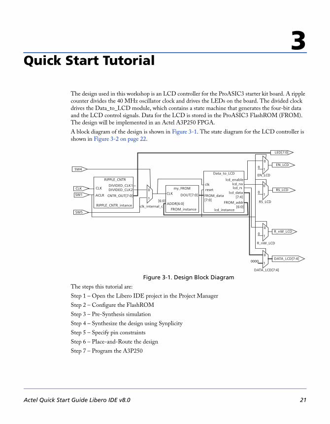
The design used in this workshop is an LCD controller for the ProASIC3 starter kit board. A ripple counter divides the 40 MHz oscillator clock and drives the LEDs on the board. The divided clock drives the Data_to_LCD module, which contains a state machine that generates the four-bit data and the LCD control signals. Data for the LCD is stored in the ProASIC3 FlashROM (FROM). The design will be implemented in an Actel A3P250 FPGA.
A block diagram of the design is shown in Figure 3-1. The state diagram for the LCD controller is shown in Figure 3-2 on page 22.
Figure 3-1. Design Block Diagram
The steps this tutorial are:
Step 1 – Open the Libero IDE project in the Project Manager
Step 2 – Configure the FlashROM
Step 3 – Pre-Synthesis simulation
Step 4 – Synthesize the design using Synplicity
Step 5 – Specify pin constraints
Step 6 – Place-and-Route the design
Step 7 – Program the A3P250
SW4
CLK
SW1
SW5
RIPPLE_CNTR
CLK
ACLR
DIVIDED_CLK1DIVIDED_CLK2
CNTR_OUT[7:0]
RIPPLE_CNTR_intance clk_internal_c
0
1[6:0]
my_FROMCLK
ADDR[6:0]
DOUT[7:0]
FROM_instance
Data_to_LCD
clkreset
FROM_data[7:0]
lcd_enable
lcd_rslcd_rw
lcd_data[7:4]
FROM_addr[6:0]
lcd_instance
LED[7:0]
EN_LCD
EN_LCD
01
0
01
0RS_LCD
RS_LCD
01
0R_nW_LCD
R_nW_LCD
1
0DATA_LCD[7:4]
0000
DATA_LCD[7:4]
Actel Quick Start Guide Libero IDE v8.0 21

Quick Start Tutorial
Design FlowUsing the Actel Libero® Integrated Design Environment (IDE) tool suite, you will complete the
following:
• Open a Libero IDE project in the Project Manager and become familiar with the files that are displayed in the Design Explorer and File Manager tabs.
• Perform pre-synthesis simulation of the design using the included testbench.
• Synthesize the design using Synplify® AE.
• Import the netlist and pin placement constraints. Route the design using Designer.
• Program an A3P250 FPGA on the starter kit board.
Figure 3-2. LCD Module State Diagram
Step 1 – Open the Libero IDE Project in the Project Manager
1. Double-click the Libero IDE icon on the Libero IDE shortcut on the desktop of your PC.
2. From the Libero IDE File menu, choose Open Project.
3. In the Libero IDE Open Project dialog box, navigate to the directory that contains the tutorial project. For this tutorial, it is C:\Actelprj\PA3_workshop\LCD_driver. Select LCD_driver.prj.
home1
home2
warmup
setfundclear1
clear2
setmode1
setmode2write1
22 Actel Quick Start Guide Libero IDE v8.0

Step 2 – Configuring the FlashROM
Click OK to open the project (Figure 3-3). You must install and run the tutorial files on your C:\ drive in order for the simulation scripts to run correctly.
Figure 3-3. Libero IDE Open Project Dialog Box
Note: If the Tool Profile Conflict Dialog window opens, select Use the profile currently selected in Libero IDE and click OK. Accept the default settings in the Project Profile window and click OK.
The VHDL source files (Data_to_LCD.vhd, RIPPLE_CNTR.vhd, Top.vhd, and TFF.vhd) are organized under the TOP (Top.vhd) in the Project Manager Design Hierarchy tab. All the project components and user files are listed in the Files tab.
Step 2 – Configuring the FlashROM1. Click the SmartDesign button in the Project Manager Project Flow window to launch
SmartDesign.
2. Name your new SmartDesign component my_FROM, and click OK. SmartDesign opens with a Canvas view, a Connectivity grid, and a Schematic view. See the SmartDesign help for more specific information on the tool. The next steps create a FlashROM.
Actel Quick Start Guide Libero IDE v8.0 23
Quick Start Tutorial
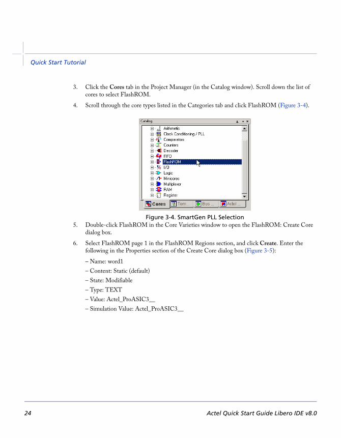
3. Click the Cores tab in the Project Manager (in the Catalog window). Scroll down the list of cores to select FlashROM.
4. Scroll through the core types listed in the Categories tab and click FlashROM (Figure 3-4).
Figure 3-4. SmartGen PLL Selection5. Double-click FlashROM in the Core Varieties window to open the FlashROM: Create Core
dialog box.
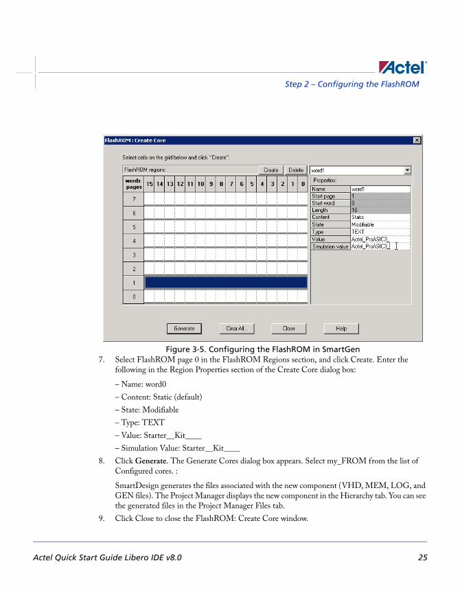
6. Select FlashROM page 1 in the FlashROM Regions section, and click Create. Enter the following in the Properties section of the Create Core dialog box (Figure 3-5):
– Name: word1
– Content: Static (default)
– State: Modifiable
– Type: TEXT
– Value: Actel_ProASIC3__
– Simulation Value: Actel_ProASIC3__
24 Actel Quick Start Guide Libero IDE v8.0
Step 2 – Configuring the FlashROM
Figure 3-5. Configuring the FlashROM in SmartGen7. Select FlashROM page 0 in the FlashROM Regions section, and click Create. Enter the
following in the Region Properties section of the Create Core dialog box:
– Name: word0
– Content: Static (default)
– State: Modifiable
– Type: TEXT
– Value: Starter__Kit____
– Simulation Value: Starter__Kit____
8. Click Generate. The Generate Cores dialog box appears. Select my_FROM from the list of Configured cores. :
SmartDesign generates the files associated with the new component (VHD, MEM, LOG, and GEN files). The Project Manager displays the new component in the Hierarchy tab. You can see the generated files in the Project Manager Files tab.
9. Click Close to close the FlashROM: Create Core window.
Actel Quick Start Guide Libero IDE v8.0 25
Quick Start Tutorial
Step 3 – Pre-Synthesis Simulation of the DesignA VHDL testbench has been provided in the Libero IDE project. Follow the steps below to perform presynthesis simulation of the design.
You must first set your simulation options to incorporate the user-defined DO file included with the tutorial.
1. In the Project Manager, from the Project menu, choose Project Settings. Click the Simulation tab. Deselect the Use automatic Do file checkbox, and navigate to your user-defined DO file: run_Top.do. The default directory for the file is c:/PA3_workshop/LCD_driver/simulation/run_Top.do
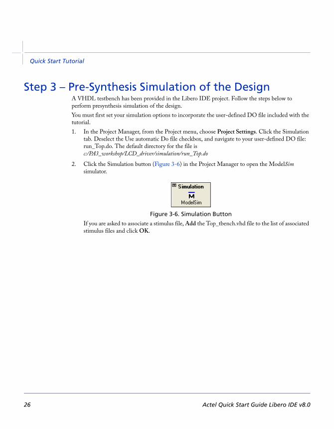
2. Click the Simulation button (Figure 3-6) in the Project Manager to open the ModelSim simulator.
Figure 3-6. Simulation Button
If you are asked to associate a stimulus file, Add the Top_tbench.vhd file to the list of associated stimulus files and click OK.
26 Actel Quick Start Guide Libero IDE v8.0
Step 4 – Synthesize the Design Using Synplicity
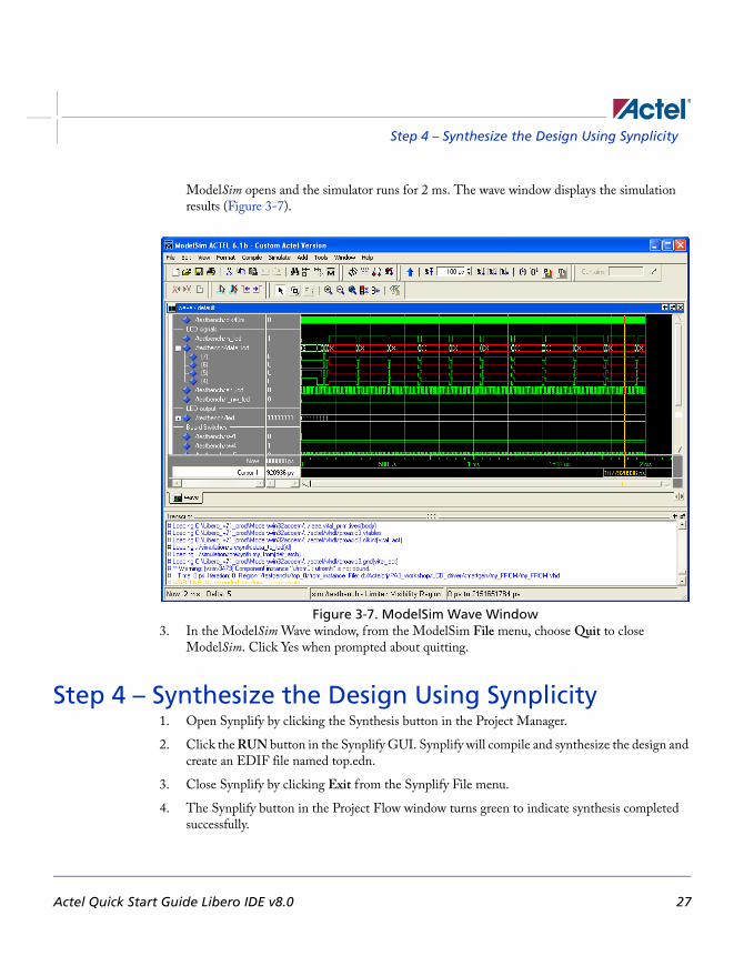
ModelSim opens and the simulator runs for 2 ms. The wave window displays the simulation results (Figure 3-7).
Figure 3-7. ModelSim Wave Window3. In the ModelSim Wave window, from the ModelSim File menu, choose Quit to close
ModelSim. Click Yes when prompted about quitting.
Step 4 – Synthesize the Design Using Synplicity1. Open Synplify by clicking the Synthesis button in the Project Manager.
2. Click the RUN button in the Synplify GUI. Synplify will compile and synthesize the design and create an EDIF file named top.edn.
3. Close Synplify by clicking Exit from the Synplify File menu.
4. The Synplify button in the Project Flow window turns green to indicate synthesis completed successfully.
Actel Quick Start Guide Libero IDE v8.0 27

Quick Start Tutorial
Step 5 – Specify Pin ConstraintsA constraint file containing pin assignments has been included in the Libero IDE project. The constraint file Top.pdc is visible in the Project Manager Files tab, listed under Constraint Files. Follow the steps below to direct the Project Manager to send the constraint file and the EDIF netlist created in Step 4 to the place-and-route tool.
1. In the Project Manager, from the Project menu, choose File Organization > Designer Constraint Files.
2. In the Organize Constraints for Designer dialog box, select Top.pdc and click Add (Figure 3-8).
3. Click OK in the Organize Constraints for Designer dialog box. The Project Manager will send the constraint file and the EDIF netlist to the place-and-route tool.
Figure 3-8. Selecting the Constraint File for Place-and-Route
Step 6 – Place-and-Route the Design1. Click the Place-and-Route button in the Project Manager to open Designer.
2. When Designer opens, click Next to accept the default settings in the Designer Device Selection Wizard dialog box.
3. Click Next to accept the default settings in the Device Selection Wizard – Variations dialog box.
28 Actel Quick Start Guide Libero IDE v8.0

Step 6 – Place-and-Route the Design
4. Click Finish to accept the default settings in the Device Selection Wizard – Operating Conditions dialog box. The Designer GUI appears (Figure 3-9).
Figure 3-9. Designer GUI5. Click the Compile button in the Designer GUI to compile the Design. Click OK in the
Compile Options dialog box to run the compiler. The Compile button in the Designer GUI turns green to indicate the design was compiled successfully.
6. Click the I/O Attribute Editor button in the Designer GUI to open the I/O Attribute Editor.
Observe the I/O settings for the pins in the design. Note that the pin assignments from the constraint file have been assigned. Close the I/O Attribute editor.
7. Click the Layout button in the Designer GUI.
8. Accept the default settings in the Layout Options window and click OK to start layout. When layout completes, the Layout button in the Designer GUI turns green.
Actel Quick Start Guide Libero IDE v8.0 29

Quick Start Tutorial
9. Click the Programming File button, and confirm that the following are checked in the Silicon Feature(s) to be Programmed section:
– FPGA Array
– FlashROM
Accept the default location for the FlashROM configuration file and click Next.
10. Confirm that pages 0 and 1 are checked in the Program Page column of the FlashROM Settings dialog box and click Finish.
11. From the File menu, choose Exit to close Designer. Select Yes if you are prompted about saving your changes.
Step 7 – Programming the A3P2501. Move the switch to ON to apply power to the board.
2. Launch the FlashPro software from the Project Manager by clicking the Programming button.
3. Click the Configure STAPL File button in the FlashPro GUI.
4. Select Program from the Action list in the Single STAPL Configuration dialog box.
5. Click the Program button in the FlashPro 4.0 main GUI to program the device.
The Programming Status column in the Programmer list window indicates the programming progress. The Status will change to Run Passed to indicate that programming completed successfully.
Note: Do not interrupt the programming sequence; it may damage the device or the programmer.
6. Close FlashPro.
7. Observe the LDC display on the ProASIC3 starter kit board (if available).
30 Actel Quick Start Guide Libero IDE v8.0

4Design Considerations
This chapter contains information and procedures to assist you in creating Actel designs.
Naming ConventionsThis section lists schematic, Verilog, and VHDL naming conventions that should be followed to avoid potential design flow problems.
SchematicUse only alphanumeric and underscore “_” characters for schematic net and instance names. Do not use asterisks, forward slashes, backward slashes, spaces, or special characters ($, #, @, !, ( ), *, &, %, etc.). Refer to the Libero online help for more information on schematic naming conventions.
VHDLIf simulation is to be completed using a VHDL simulator, it is important to create schematics or write HDL code that complies with the VHDL naming conventions. The following naming conventions apply to VHDL designs:
• VHDL is not case sensitive.
• Two dashes “--” are used to begin comment lines.
• Names can use alphanumeric characters and the underscore “_” character.
• Names must begin with an alphabetic letter.
• Do not use two underscores in a row, or use an underscore as the last character in the name.
• Spaces are not allowed within names.
• Object names must be unique. For example, you cannot have a signal named A and a bus named A(7 downto 0).
VHDL Keywords
The following is a list of the VHDL reserved keywords:
abs downto library postponed subtype
access else linkage procedure then
after elsif literal process to
Actel Quick Start Guide Libero IDE v8.0 31

Design Considerations
VerilogIf simulation is to be completed using a Verilog simulator, it is important to create schematics or write HDL code that complies with the Verilog naming conventions. The following naming conventions apply to Verilog HDL designs:
• Verilog is case sensitive.
• Two slashes “//” are used to begin single line comments. A slash and asterisk “/*” are used to begin a multiple line comment and an asterisk and slash “*/” are used to end a multiple line comment.
• Names can use alphanumeric characters, the underscore “_” character, and the dollar “$” character.
alias end loop pure transport
all entity map range type
and exit mod record unaffected
architecture file nand register units
array for new reject until
assert function next rem use
attribute generate nor report variable
begin generic not return wait
block group null rol when
body guarded of ror while
buffer if on select with
bus impure open severity xnor
case in or shared xor
component inertial others signal
configuration inout out sla
constant is package sra
disconnect label port srl
32 Actel Quick Start Guide Libero IDE v8.0

Naming Conventions
• Names must begin with an alphabetic letter or the underscore.
• Spaces are not allowed within names.
Verilog Keywords
The following is a list of Verilog reserved keywords:
always endfunction macromodule realtime tran
and endmodule medium reg tranif0
assign endprimitive module release tranif1
attribute endspecify nand repeat tri
begin endtable negedge rnmos tri0
buf endtask nmos rpmos tri1
bufif0 event nor rtran triand
bufif1 for not rtranif0 trior
case force notif0 rtranif1 trireg
casex forever notif1 scalared unsigned
casez fork or signed vectored
cmos function output small wait
const highz0 parameter specify wand
deassign highz1 pmos specparam weak0
default if posedge strength weak1
defparam ifnone primitive strong0 while
disable initial pull0 strong1 wire
edge inout pull1 supply0 wor
else input pulldown supply1 xnor
end integer pullup table xor
Actel Quick Start Guide Libero IDE v8.0 33
Design Considerations
Hierarchical DesignsMultiple-level or hierarchical designs are created by creating symbolic representations of blocks and adding them to other levels. The Designer software reads and writes hierarchical netlists.
Multiple Sheet DesignsThe Designer software supports multiple sheet designs. Each sheet in the design is considered as part of a schematic, and it is not considered as a level of hierarchy. Most schematic capture tools have page connectors to connect the sheets. Refer to the documentation provided with your schematic capture tool for additional information.
Actel LibrariesActel provides libraries to support schematic- and synthesis-based designs. Logic can be described in behavioral languages (VHDL or Verilog). Structured logic such as counters, adders, and comparators can be automatically built using the core builder included with the Libero IDE. Functions can be exclusively behavioral, schematic, or a combination of the two. Timing definition is supported by the timing driven layout tools. I/O definitions can be described in the design source or in Designer.
Adding Power and GroundActel provides special VCC and GND macros to connect nets to power and ground. Add the VCC and GND macros to your design and connect them by nets to the functional logic making up the design. It is important to use the symbols provided by Actel in order to prevent design flow issues. Do not add power and ground to designs by naming nets or adding third-party power and ground symbols. Refer to the Actel Interface Guides or the Libero IDE online help for information about adding power and ground to your design.
endattribute join remos task
endcase large real time
34 Actel Quick Start Guide Libero IDE v8.0
Adding a Global Network
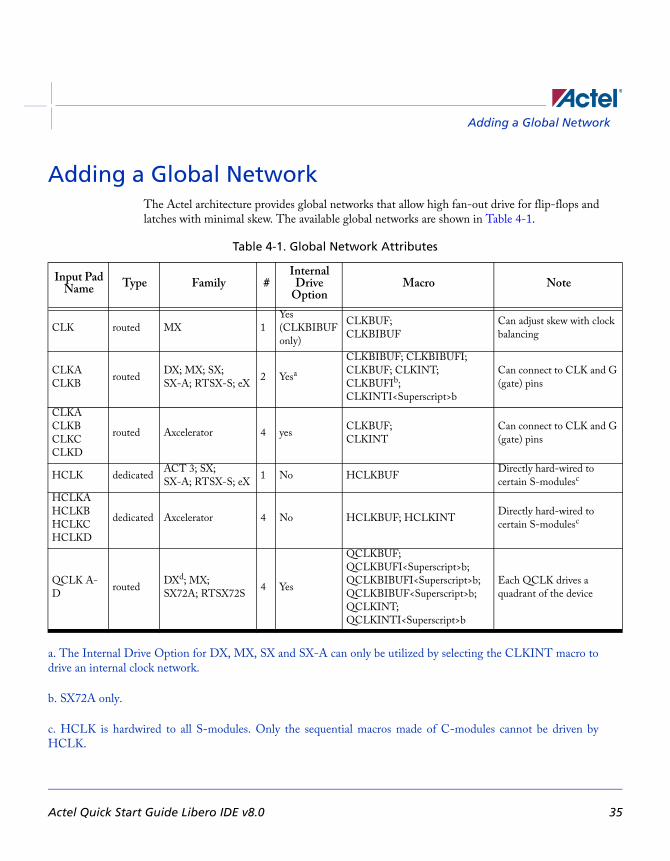
Adding a Global NetworkThe Actel architecture provides global networks that allow high fan-out drive for flip-flops and latches with minimal skew. The available global networks are shown in Table 4-1.
Table 4-1. Global Network Attributes
Input Pad Name Type Family #
Internal Drive
OptionMacro Note
CLK routed MX 1
Yes
(CLKBIBUFonly)
CLKBUF;
CLKBIBUF
Can adjust skew with clock
balancing
CLKA
CLKBrouted
DX; MX; SX;
SX-A; RTSX-S; eX2 Yesa
CLKBIBUF; CLKBIBUFI;
CLKBUF; CLKINT;
CLKBUFIb; CLKINTI<Superscript>b
Can connect to CLK and G
(gate) pins
CLKA
CLKB
CLKCCLKD
routed Axcelerator 4 yesCLKBUF;
CLKINT
Can connect to CLK and G
(gate) pins
HCLK dedicatedACT 3; SX;
SX-A; RTSX-S; eX1 No HCLKBUF
Directly hard-wired to
certain S-modulesc
HCLKA
HCLKB HCLKC
HCLKD
dedicated Axcelerator 4 No HCLKBUF; HCLKINTDirectly hard-wired to certain S-modulesc
QCLK A-
Drouted
DXd; MX;
SX72A; RTSX72S4 Yes
QCLKBUF;
QCLKBUFI<Superscript>b; QCLKBIBUFI<Superscript>b;
QCLKBIBUF<Superscript>b;
QCLKINT; QCLKINTI<Superscript>b
Each QCLK drives a
quadrant of the device
a. The Internal Drive Option for DX, MX, SX and SX-A can only be utilized by selecting the CLKINT macro todrive an internal clock network.
b. SX72A only.
c. HCLK is hardwired to all S-modules. Only the sequential macros made of C-modules cannot be driven byHCLK.
Actel Quick Start Guide Libero IDE v8.0 35
Design Considerations
Routed ClocksRouted clocks are clock networks with unlimited fan-out and offer clock speeds that are independent of the number of logic modules being driven. Routed clocks can be used as RESET and PRESET networks to drive the reset and preset pins of internal logic modules. They can also be connected to most logic module inputs.
CLK, CLKA, CLKB
CLK, CLKA, CLKB, CLKC1, and CLKD1 are routed global clocks that can be used by selecting the CLKBUF, CLKBIBUF, CLKBIBUFI, CLKINT, or CLKINTI macro.
QCLK
QCLK (available on 42MX, 24MX36, 42MX36, 3200DX, and 54SX72A devices) is a routed quadrant or global clock that can drive from one to four quadrants on a device. In addition to global RESET and PRESET networks, QCLK can be used as a quadrant RESET and PRESET network. QCLK can be used by selecting the QCLK, QCLKINT, QCLKINTI, QCLBUF, QCLBUFI, QCLBIBUF, QCLBIBUFI macro.
Note: QCLK is not available for Axcelerator.
Dedicated ClocksDedicated clocks are clock networks that are directly wired to either sequential or I/O modules. They contain no programming elements in the path from the I/O pad driver to the input of sequential or I/O modules. These clocks provide sub-nanosecond skew and guaranteed performance.
HCLK
HCLK (HCLKA, HCLKB, HCLKC, and HCLKD for Axcelerator devices) is a dedicated hard-wired clock input for sequential modules. HCLK is directly wired to each sequential module and offers clock speeds independent of the number of sequential modules being driven. HCLK can be used by selecting the HCLKBUF macro. Table 4-2 lists the ACT 3 sequential elements and Table
d. Not available in 32140DX, 3265DX
1. Axcelerator only.
36 Actel Quick Start Guide Libero IDE v8.0

Adding a Global Network
4-3 lists the SX/SX-A/eX sequential elements that cannot be connected to HCKLBUF because they are built from combinatorial modules.
IOCLK1
IOCLK is a dedicated hard-wired clock input for I/O modules. IOCLK is directly wired to each I/O module register and offers speeds independent of the number of I/O modules being driven. IOCLK can be used by selecting the IOCLKBUF macro.
Special ClocksSpecial clocks are special hard-wired networks for I/O modules that can only drive preset/clear pins of I/O modules. IOPCL1, the only special clock, is a special network directly wired to the preset and clear inputs of all I/O registers. IOPCL functions as an I/O when no I/O preset or clear macros are used. IOPCL can be used by selecting the IOPCLBUF macro.
PLL
PLLs (Phase-Locked Loops) are dedicated clock resources that are available for the ProASIC3/E, ProASICPLUS (two PLLs), and Axcelerator families. Each Axcelerator device has eight PLLs; four PLLs may be used on the HCLK network and four PLLs may be used on the routed clock network.
Use PLLs to reduce the skew on the clock network. PLLs can accept feedback from internal and external clock sources, and used to multiply, divide, and phase-shift clocks internally. You can also cascade your PLLs to obtain a specific clock frequency.
Table 4-2. ACT 3 Sequential Elements that Cannot Connect to HCKLBUF
DFP1 DFP1B DFP1D DFPCA DFPC DLC1
DLC1A DLC1F DLC1G DLE2C DLE3B DLE3C
DLP2C DLP1A DLP1B DLP1C DFP1A
Table 4-3. 54SX/54SX-A/eX Sequential Elements that Cannot Connect to HCKLBUF
DLC1 DLC1A DLC1F DLC1G DLE2C DLE3B
DLE3C DLP2C DLP1A DLP1B DLP1C DFP1A
1. IOCLK and IOPCL are only available in the DX/42MX family.
Actel Quick Start Guide Libero IDE v8.0 37

Design Considerations
Using ProASIC and ProASICPLUS Global Routing ResourcesUse the automatic global resource assignments specified by Designer. These lines exhibit very low skew. When Designer imports the netlist and device data, it can automatically assign unused global resources to the nets with the highest fan-outs (for example, clock and reset signals).
If high fan-out signals mapped by Designer to global resources are buffered, Designer automatically removes these buffers. Flash devices provide automatic buffering for global resources.
Signals can also be assigned to the global resources by using Designer global primitives in netlists, and by specifying constraint files for Designer.
The checker contains a description of the highest fan-out nets in a design and the results of automatic global assignments. If your constraints appear not to have been honored, refer to this report file.
CombinabilityThe functionality of some combinations of gates and flip-flops can be combined to fit into a single logic module instead of a logic module to implement each gate or flip-flop. This ability is called combinability. Designer has an automatic utility called the Combiner to perform this function, as well as to reduce the logic in other ways.
The Combiner reduces the number of logic modules, logic levels, and fan-ins in a design by remapping, removing, and combining certain hard macros, including the deletion of buffers on clock networks. It also simplifies a design netlist using features of the Actel architecture.
The Combiner is integrated into the Compile function in Designer. It improves the density, speed, and routability of a design by performing the following functions:
• Combinatorial Module Reduction
• Sequential Remapping
• Unused Logic Removal
• Constant Input Reduction
• Fan-in Reduction
• I/O-Register Combining in Axcelerator (see the Axcelerator datasheet at http://www.actel.com/documents/axds.pdf for more information)
• I/O-FIFO Combining in Axcelerator (see the Axcelerator datasheet for more information)
38 Actel Quick Start Guide Libero IDE v8.0

Combinability
Combinatorial Module ReductionCombinatorial Module Reduction reduces the number of combinatorial modules and logic levels, giving a design more density and speed. It does this in one of the following two ways:
1. It combines two or more combinatorial macros into a single macro. For example, two 2-input AND gates, two inverters, and three inverters are combined into a single 3-input AND gate, a buffer, and an inverter respectively, shown in Figure 4-1.
2. It combines a combinatorial macro and a sequential macro into a single sequential macro. For example, a combinatorial macro “MUX” and a sequential macro “DF1” are combined into a single sequential macro “DFM,” shown in Figure 4-2. Module Reduction is not available for 54SX/54SX-A or eX devices. Instead, an automatic DirectConnect between a combinatorial module and a sequential module is used.
Sequential RemappingSequential Remapping attempts to achieve better results in the density, speed and routability of a design. If Sequential Remapping cannot reduce the total number of combinatorial macros in the
Becomes
Becomes
Becomes
Figure 4-1. Combined Combinatorial Macros
MUXDF1
A
B
clk
B
clk
A
S DFMBecomes
S
Figure 4-2. Combined Combinatorial and Sequential Macros
Actel Quick Start Guide Libero IDE v8.0 39

Design Considerations
design, the Combiner does not use it. Sequential Remapping is not available for MX devices because these families do not have sequential modules. Sequential Remapping is not available for SX/SX-A or eX devices because the sequential modules in SX/SX-A and eX do not have a combinatorial component. Instead, optimal performance is achieved by an automatic DirectConnect between a combinatorial module and a sequential module whenever possible. Sequential Remapping performs the following three steps in order:
1. It divides complex sequential library macros into basic combinatorial and sequential macros. For example, a D-type flip-flop with 2-input multiplexed data “DFM” remaps into a 2 to 1 multiplexor “MX2” and a D-type flip-flop “DF1.” The total number of logic modules has temporarily increased from one combinatorial and one sequential module to two combinatorial and one sequential module, shown in Figure 4-3.
2. It implements the new combinatorial macro by combining the basic combinatorial macro from step 1 with its previous combinatorial macro in a design. For example, “MX2” and an inverter “INV” are combined into “MX2A.” The total number of logic modules is decreased to one combinatorial and one sequential module, shown in Figure 4-4.
3. It combines the new combinatorial macro from step 2 with the basic sequential macro from step 1. For example, “MX2A” and “DF1” are combined into a D type flip-flop with 4 input
MX2 DF1
A
B
clk
B
clk
A
S
DFM
XYZ
X
Y
Z
SD Q
Becomes
INV INV
Figure 4-3. Complex Macros Divided
MX2 DF1
A
B
clk
X
Y
Z
SD Q
Becomes
MX2A DF1
A
B
clk
X
Y
Z
SD Q
INV
Figure 4-4. Logic Modules Decreased
40 Actel Quick Start Guide Libero IDE v8.0

Combinability
multiplexed data, active low clear, and active high clock “DFM6A.” The total number of logic modules is further decreased to one sequential module, shown in Figure 4-5.
Figure 4-5. Logic Reduced to One Sequential Module
Unused Logic RemovalUnused Logic Removal removes all logic macros that are not driving any other logic macro input or do not propagate to an output pad. The removal of such macros does not affect the functionality of the circuit. An example of Unused Logic Removal is shown in Figure 4-6.
Figure 4-6. Unused Logic Removal
Constant Input ReductionEvery Actel hard macro can be mapped or configured in many different ways to implement logic functions. However, when macro inputs are tied to power or ground, the number of configurations available to the place-and-route software is decreased. Constant Input Reduction reconfigures macros that have unused inputs connected to power or ground into logically equivalent functions with the power or ground connections eliminated. Constant Input Reduction only reconfigures
Becomes
MX2A
DF1
A
B
clk
X
Y
Z
SD Q
clkS1
DFM6A
Z
Q
VDD
CLRclk
S0
D3
D0D1D2
VDDGND
Y
X
Becomes
CLK
D Q
CLK
D Q
Actel Quick Start Guide Libero IDE v8.0 41

Design Considerations
combinatorial macros. Sequential macros that have inputs connected to power or ground are not affected. Figure 4-7 illustrates how Constant Input Reduction is achieved.
Fan-in ReductionFan-in Reduction reduces the number of inputs of a combinatorial macro that has inputs tied together by mapping it to a logically equivalent macro with fewer inputs. This function substantially improves the routability of a design. Fan-in Reduction does not reduce the number of logic modules and only reconfigures combinatorial macros. Sequential macros that have inputs tied together are not affected. Figure 4-8 illustrates Fan-in Reduction.
Back-Annotation EffectsThe Combiner does not change the functionality of a design. Rather, it improves the density, speed and routability of a design. Changes resulting from logic removal or combining are not visually back annotated to the schematic, but the timing is adjusted accordingly. The removal or combining of logic does not adversely affect either back annotation to a simulator or timing analysis performed by Timer.
Becomes
Figure 4-7. Constant Input Reduction
Becomes
Figure 4-8. Fan-in Reduction
42 Actel Quick Start Guide Libero IDE v8.0
Combinability
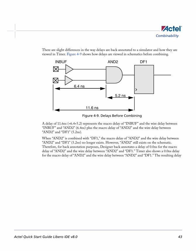
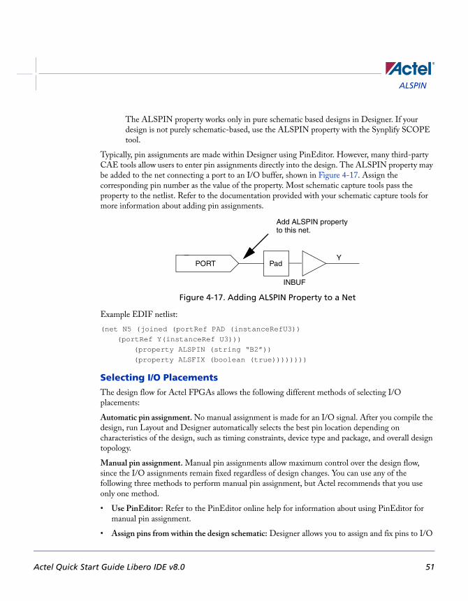
There are slight differences in the way delays are back annotated to a simulator and how they are viewed in Timer. Figure 4-9 shows how delays are viewed in schematics before combining.
A delay of 11.6ns (=6.4+5.2) represents the macro delay of “INBUF” and the wire delay between “INBUF” and “AND2” (6.4ns) plus the macro delay of “AND2” and the wire delay between “AND2” and “DF1” (5.2ns).
When “AND2” is combined with “DF1,” the macro delay of “AND2” and the wire delay between “AND2” and “DF1” (5.2ns) no longer exists. However, “AND2” still exists on the schematic. Therefore, for back annotation purposes, Designer back annotates a delay of 0.0ns for the macro delay of “AND2” and the wire delay between “AND2” and “DF1.” Timer also shows a 0.0ns delay for the macro delay of “AND2” and the wire delay between “AND2” and “DF1.” The resulting delay
AND2 DF1
6.4 ns
5.2 ns
INBUF
11.6 ns
Figure 4-9. Delays Before Combining
Actel Quick Start Guide Libero IDE v8.0 43
Design Considerations
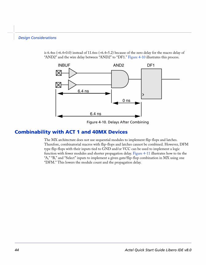
is 6.4ns (=6.4+0.0) instead of 11.6ns (=6.4+5.2) because of the zero delay for the macro delay of “AND2” and the wire delay between “AND2” to “DF1.” Figure 4-10 illustrates this process.
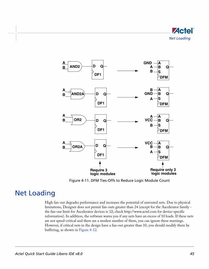
Combinability with ACT 1 and 40MX DevicesThe MX architecture does not use sequential modules to implement flip-flops and latches. Therefore, combinatorial macros with flip-flops and latches cannot be combined. However, DFM type flip-flops with their inputs tied to GND and/or VCC can be used to implement a logic function with fewer modules and shorter propagation delay. Figure 4-11 illustrates how to tie the “A,” “B,” and “Select” inputs to implement a given gate/flip-flop combination in MX using one “DFM.” This lowers the module count and the propagation delay.
AND2 DF1
6.4 ns
INBUF
0 ns
6.4 ns
Figure 4-10. Delays After Combining
44 Actel Quick Start Guide Libero IDE v8.0
Net Loading
Net LoadingHigh fan-out degrades performance and increases the potential of unrouted nets. Due to physical limitations, Designer does not permit fan-outs greater than 24 (except for the Axcelerator family - the fan-out limit for Axcelerator devices is 32; check http://www.actel.com for device-specific information). In addition, the software warns you if any nets have an excess of 10 loads. If these nets are not speed-critical and there are a modest number of them, you can ignore these warnings. However, if critical nets in the design have a fan-out greater than 10, you should modify them by buffering, as shown in Figure 4-12.
D Q
D Q
D Q
D Q
DF1
AND2
AND2A
OR2A
GND
VCC
GND
DFM
ABS
OR2
DF1
DF1
DF1
Q
DFM
ABS
Q
DFM
ABS
Q
DFM
ABS
QVCC
AB
B
A
A
B
BA
Require 3 Require only 2
AB
AB
AB
AB
logic moduleslogic modules
Figure 4-11. DFM Ties-Offs to Reduce Logic Module Count
Actel Quick Start Guide Libero IDE v8.0 45

Design Considerations
An alternative method to buffering is duplicating logic to eliminate the buffer delay, shown in Figure 4-13.
Both buffering and duplicating logic cost additional logic modules. You can use buffering if you are not concerned about the skew or if you want to minimize the amount of logic resources used, because buffering generally takes less logic than logic duplication. However, Actel recommends that you duplicate logic to reduce fan-out because it does not add an additional delay in the form of a buffer and it reduces skew.
Logic and I/O UtilizationThe Designer software calculates the logic module and I/O module utilization. You can view module utilization by generating a Status report.
To improve the chances of optimal routing, Actel recommends that the total logic module utilization be between 50% and 85%.
• Lower utilization, especially with high I/O usage, causes excessively long delays and, possibly, unrouted nets.
• High utilization should be avoided if there is significant use of high pin count macros (for example, “MX4” and “DFM6A”).
Figure 4-12. Buffering
FO=18 FO=9FO=10
FO=18 FO=9
FO=9
Figure 4-13. Duplicating Logic
46 Actel Quick Start Guide Libero IDE v8.0

Adding Properties
If the design requires additional resources, you can use a larger device by changing the device and package selection within Designer. The specialized I/O macros take advantage of architectural enhancements with the later families. Use these macros to improve performance.
Refer to the Actel datasheet for your device and the Antifuse, ProASIC/ProASICPLUS, and
ProASIC3/E Macro Library guides for additional information. Also, refer to the Actel website at http://www.actel.com for more information on routability.
Adding PropertiesThis section describes how to add properties to your designs.
Note: ALSPIN and ALSPRESERVE are not available for ProASIC3/E, ProASICPLUS, or ProASIC devices.
ALSPRESERVEWhen Designer compiles a design, one of the functions of the Combiner is to combine (optimize) combinatorial functions into sequential macros whenever possible. Combining logic does not affect the functionality of the circuit. To prevent such combining, an “ALSPRESERVE” property may be added to the net connecting the macros that would otherwise be combined, as shown in Figure 4-14. The “ALSPRESERVE” property does not need to have a value assigned to it. Most schematic capture tools pass the property to the netlist. Refer to the documentation provided with your schematic capture tools for information about adding properties to nets.
Figure 4-14. Adding ALSPRESERVE Property to a Net
Example EDIF netlist:
(net N4 (joined (portRef Y (instanceRefU2))(portRef D (instanceRef U3)))
(property ALSPRESERVE (boolean (true))))
N4
U3
Add ALSPRESERVEproperty to this net
U2
Actel Quick Start Guide Libero IDE v8.0 47

Design Considerations
BUFD and INVD Delay MacrosThe suggested uses of BUFD and INVD are as follows:
• Maintain the phase relationship between clock and data input signals when sending signals derived from them these signals off-chip. This application enables them to meet external setup and hold requirements.
• Maintain the phase relationship of clock and data input signals in designs with high-fan-out clock signals.
Note: Our Flash devices do not support these delay macros.
Maintaining Phase Relationships
As shown in Figure 4-15, a certain phase relationship exists between the clock and data signals (generally, the data signal lags the clock signal). Actel recommends you employ BUFD to maintain this phase relationship. All Actel antifuse device families have a restriction that a CLKBUF cannot be connected directly to an OUTBUF, so Designer software automatically inserts a BUFF module (inst3 in Figure 4-15). This introduces a delay that may cause the data signal to arrive ahead of the sys_clk signal going off-chip. To prevent this, you can insert a BUFD macro in your netlist. The BUFD, unlike a regular BUFF, is assigned the ALSPRESERVE property. This ensures that the BUFD is not optimized away during the compilation step and hence can offset the delay caused by automatic insertion of the BUFF in the sys_clk path. This technique maintains the phase relationship of the data andclock inputs when going off-chip and the external setup and hold requirements can be met.
Figure 4-15. Phase Relationship Control - Data and System Clock using BUFD
In Figure 4-16, the clock signal coming from the CLKBUF has a high fan-out. This means increased capacitive loading and hence increased delay. In contrast, the data signal has a fan-out of
D
FF
data
CLK
inst1
inst2
inst3
BUFD
BUFF inserted by Designer Software
OUTBUF
OUTBUF
INBUF
CLKBUF
Q out 1
out 2
CLK
48 Actel Quick Start Guide Libero IDE v8.0
Adding Properties
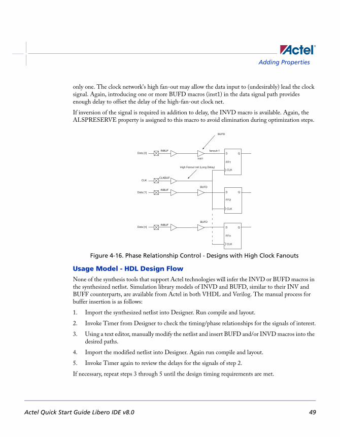
only one. The clock network's high fan-out may allow the data input to (undesirably) lead the clock signal. Again, introducing one or more BUFD macros (inst1) in the data signal path provides enough delay to offset the delay of the high-fan-out clock net.
If inversion of the signal is required in addition to delay, the INVD macro is available. Again, the ALSPRESERVE property is assigned to this macro to avoid elimination during optimization steps.
Figure 4-16. Phase Relationship Control - Designs with High Clock Fanouts
Usage Model - HDL Design Flow
None of the synthesis tools that support Actel technologies will infer the INVD or BUFD macros in the synthesized netlist. Simulation library models of INVD and BUFD, similar to their INV and BUFF counterparts, are available from Actel in both VHDL and Verilog. The manual process for buffer insertion is as follows:
1. Import the synthesized netlist into Designer. Run compile and layout.
2. Invoke Timer from Designer to check the timing/phase relationships for the signals of interest.
3. Using a text editor, manually modify the netlist and insert BUFD and/or INVD macros into the desired paths.
4. Import the modified netlist into Designer. Again run compile and layout.
5. Invoke Timer again to review the delays for the signals of step 2.
If necessary, repeat steps 3 through 5 until the design timing requirements are met.
D
FF1
Q
CLK
D
FF2
Q
CLK
D
FFn
Q
CLK
BUFD
INBUFData [0]
inst1
fanout=1
CLK
Data [1]INBUF
INBUF
CLKBUF
Data [n]
High Fanout net (Long Delay)
BUFD
BUFD
Actel Quick Start Guide Libero IDE v8.0 49
Design Considerations
Usage Models - Schematic Capture Design Flow
INVDs and BUFDs are available for the following Actel-supported schematic capture tools:
• ConceptHDL PE13.5 and PE13.6
• Mentor Graphics c.4 and D.1
• ePD 1.1/2.0
To avoid inadvertent instantiation of INVD or BUFD where INV or BUFF is intended, the graphical symbols for INVD and BUFD have warning labels "Special Use Only."
The flow for buffer insertion is as follows:
1. Generate an EDIF netlist with the schematic tool.
2. Import the EDIF netlist into Designer. Run compile and layout.
3. Invoke Timer from Designer to check the timing/phase relationships for the signals of interest.
4. Edit the schematics to insert BUFD and/or INVD macros into the desired paths.
5. Check and save your schematics. Generate an EDIF netlist from the modified schematics.
6. Import the modified netlist into Designer. Again run compile and layout.
7. Invoke Timer again to review the delays for the signals of step 3.
8. If necessary, repeat steps 4 through 7 until the design timing requirements are met.
Delay Values
Rising (R) and falling (F) delays for INVD and BUFD in different Actel families can be found in the relevant datasheets. These values are obtained using the fastest speed grade for the device using typical temperature, voltage, and process corners as well as optimized placement. Actual delay numbers may vary with the device, speed grade, and actual placement. Please visit our website at http://www.actel.com/documents/BUFD.pdf for more information.
ALSPINActel provides special input, output, tri-state, and bi-directional macros for adding I/Os to your design. Add the I/O macros to your design and connect them by nets to both port symbols, and the functional logic making up the design. Most third-party CAE tools have special symbols to represent the ports. Refer to the Actel Interface Guides for information about adding I/Os to your design.
Note: ProASIC and ProASICPLUS devices do not support the ALSPIN property.
50 Actel Quick Start Guide Libero IDE v8.0
ALSPIN
The ALSPIN property works only in pure schematic based designs in Designer. If your design is not purely schematic-based, use the ALSPIN property with the Synplify SCOPE tool.
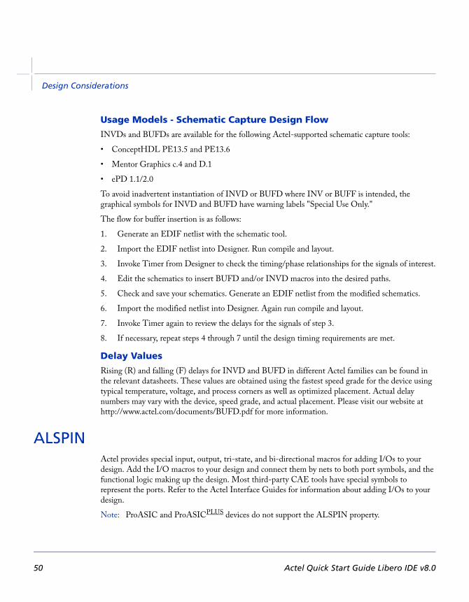
Typically, pin assignments are made within Designer using PinEditor. However, many third-party CAE tools allow users to enter pin assignments directly into the design. The ALSPIN property may be added to the net connecting a port to an I/O buffer, shown in Figure 4-17. Assign the corresponding pin number as the value of the property. Most schematic capture tools pass the property to the netlist. Refer to the documentation provided with your schematic capture tools for more information about adding pin assignments.
Figure 4-17. Adding ALSPIN Property to a Net
Example EDIF netlist:
(net N5 (joined (portRef PAD (instanceRefU3))(portRef Y(instanceRef U3)))
(property ALSPIN (string “B2”))(property ALSFIX (boolean (true))))))))
Selecting I/O Placements
The design flow for Actel FPGAs allows the following different methods of selecting I/O placements:
Automatic pin assignment. No manual assignment is made for an I/O signal. After you compile the design, run Layout and Designer automatically selects the best pin location depending on characteristics of the design, such as timing constraints, device type and package, and overall design topology.
Manual pin assignment. Manual pin assignments allow maximum control over the design flow, since the I/O assignments remain fixed regardless of design changes. You can use any of the following three methods to perform manual pin assignment, but Actel recommends that you use only one method.
• Use PinEditor: Refer to the PinEditor online help for information about using PinEditor for manual pin assignment.
• Assign pins from within the design schematic: Designer allows you to assign and fix pins to I/O
Add ALSPIN property to this net.
PORT Pad
INBUF
Y
Actel Quick Start Guide Libero IDE v8.0 51

Design Considerations
signals in your design schematic. For more information on how to assign pins from within the design schematic, refer to the Actel Interface Guides. You cannot back annotate pin assignments from Designer to your design schematic.
• Import the <design>.pin file into Designer: Designer can import pin files to assign pins. Refer to the Designer online help for more information on how to import a file into Designer.
Note: For Axcelerator, the PDC file replaces the PIN file.
For Flash devices, the GCF file replaces the PIN file.
How you use the three methods above depends on the requirements of the project. You can get the final pin assignment by generating a pin report and/or printing the graphical view of the device pin assignment in PinEditor.
Suggested I/O Assignment MethodBecause both methods (automatic or manual) of determining I/O pin assignments for Actel devices can be used in combination, there are many methods to create quality pin placements. The best method for a design depends on factors such as scheduling constraints, design changes, and performance specifications.
To design effectively, use automatic pin assignment for 100% of theI/O signals. Designer optimizes the place-and-route, especially if it is given the flexibility of automatically assigning all I/O placements. Designer selects, evaluates, and optimizes many different I/O configurations specific to the device architecture. If as few as 10% of the pin assignments are inefficiently assigned manually, the quality of the place-and-route could be compromised. Fixed manual assignments should be kept to a minimum.
Note: Automatic pin assignment may not be suitable for Axcelerator because of I/O bank assignments. Please see the PinEditor online help for more information on I/O bank assignments.
Fast I/O Assignment ProcedureThe I/O assignment process does not have to be a gating item to the overall system schedule. The optimal design flow allows the software to reposition the I/O every design iteration. However, as long as I/O assignments change, PCB layout cannot take place, and the board may take several weeks to manufacture. To save time, as long as the number and function of the I/Os are finalized, use the following procedure to have Designer automatically assign all of the pins before the details of the design are completed and before the design is completely tested and debugged.
1. Enter the design as completely as possible, ignoring small details to be modified later. It is important to include all of the major functions that will be in the FPGA circuit. The objective is to obtain a netlist that approximates the final design topology. The circuit does not need to be
52 Actel Quick Start Guide Libero IDE v8.0

ALSPIN
functionally correct at this point but must have the same major functional blocks (adders, counters, and so on) and approximately the same number of logic modules as the final design.
2. Layout the design in Designer. Ignore any warnings from the Compile program that may be attributed to the unfinished state of the design. Run Layout in standard mode with incremental placement turned off.
At this point, Layout has automatically assigned I/Os according to the design topology. This is done before all of the functional bugs have been discovered and resolved. Minor functional changes that may be made to the design will have little effect on the quality and effectiveness of the pin placements.
3. Layout the PCB. Complete the PCB layout knowing that the pin assignments for the Actel device will not require modifications in the future.
Layout does not modify any I/O placements that have been fixed. This method can be used even if the I/Os are manually assigned. The results of automatic I/O assignment by Layout can be used as a template for manual I/O assignment. The automatic placements can be used as a guide and small modifications can be made as required.
Assigning I/Os ManuallyIf any or all of the I/O placements must be assigned manually, a broader knowledge of Actel FPGA architecture is required. Refer to the Actel datasheets for specific devices for information about different architectures of the Actel families. The structure of the logic and I/O modules, routing tracks, antifuses, and other architectural details are discussed. This information can be used to assign I/O signals manually with the specific details of the device in mind.
During the process of assigning I/Os for the device, the following guidelines can help to increase routability and performance:
• Try to force signal paths, especially large data buses, to flow horizontally across the die, since there are more horizontal (than vertical) routing resources. In most cases, a large data bus requires many interconnections as it traverses the circuit.
The horizontal and vertical orientation of the die is the same as shown in the package pin assignment and mechanical detail drawings in the Actel datasheets.
I/O Standard Compatibility
• Count the number of levels of logic between I/Os to determine placement. For example, I/Os that are separated by one gate should be placed closer than I/Os that are separated by a long shift register. In general, the Actel device architecture allows signals to be routed across two vertical rows and over one-third of the columns of the device without using a long routing track. For example, consider an A1225 device that has 13 rows and 46 columns. Two I/O signals should not be placed on opposite sides of the device unless there are at least two horizontal or three vertical
Actel Quick Start Guide Libero IDE v8.0 53

Design Considerations
levels of logic between them.
• Use the top and bottom I/O pins for slow and/or local signals. The fact that there are fewer vertical routing resources should not harm the performance of these signals.
• Use the global clock buffers. Each of these pins is connected to a dedicated, low-skew distribution network that is optimized for high fan-out signals.
• For Axcelerator, be sure make the assignments to I/O banks with the appropriate I/O technology.
Unused I/O PinsEvery I/O bond pad on the die is connected to a multipurpose circuit capable of becoming an input, output, or tri-state I/O. The circuit is always connected to the bond pad, and Designer configures it according to the design’s specification. Refer to http://www.actel.com/custsup/search.html and search the keyword “unused” for more information.
Note: This option is not available for Axcelerator devices.
Using Probe Pins as I/O PinsLayout automatically avoids using the probe pins unless you have fixed pin assignments to one or more of these pins, or the number of pins in the design exceeds the number of non-probe I/O pins. The function of the probe pins depends on the JTAG mode Pin and Security Fuse Configuration. The availability and functionality of pins varies by device family. Please refer to the family-specific datasheets for precise data specifications (Axcelerator probe pins are dedicated). To use probe pins and JTAG pins as I/Os:
• Avoid using PRA or PRB as Input or Bidirectional pins, and
• Avoid using TDI/SDI, TCK/DCLK as Input or Bidirectional (using any of these pins in this way disables probing in the ACT1/40MX families)
Using JTAG Pins as I/O Pins The high-capacity devices of the DX, MX, SX and SX-A families have four JTAG pins: “TDI,” “TMS,” “TCK” and “TDO.” Layout automatically avoids using these pins as I/O pins. If you are not using the JTAG function, you can use these pins as I/O pins except TMS. In addition, SX-A and eX families have a JTAG reset pin TRST. This pin can also be used as a user I/O if it is not used for the JTAG function. For Axcelerator, the JTAG pins are dedicated and cannot be used as I/O pins.
54 Actel Quick Start Guide Libero IDE v8.0

Generating a Top-Level Symbol
Generating a Top-Level SymbolYou can create a top-level symbol for the entire design in your schematic entry tool. The pin names on the symbol must match the underlying port names. The top-level symbol must only contain pins for I/O buffers. Do not add power, ground, probe, or other special pins to the symbol. Doing so causes errors during netlist generation. Remember to update the symbol if pins change on the schematic.
Entering Constraints for Timing Driven Place-and-Route
Unique timing constraints for each signal path in a design can be specified using the Timer tool. It may only be necessary to specify the clock frequency for synchronous designs. The Timer mode typically eliminates time-consuming iterations of the design flow. Timing constraints can also be specified in a design constraint file and imported into Designer. Refer to the Timer online help for information about specifying timing constraints in Timer, and the Designer online help for information about importing a constraints file.
Estimating Pre-Layout TimingIt is often necessary to estimate the timing of a design to be implemented prior to using the design tools. With some knowledge of the critical path, you can perform this analysis using the timing information in the device-specific Actel datasheet. If you are having trouble selecting the appropriate device, contact your local sales representative.
Figure 4-18 illustrates the procedure using an ACT 2 A1225XL-1 design example with a critical path from the CLK pad to the OUT pad. The delays used come from the timing tables for the A1225XL-1 in the Actel datasheets. These values include a statistical net delay which is associated
Actel Quick Start Guide Libero IDE v8.0 55
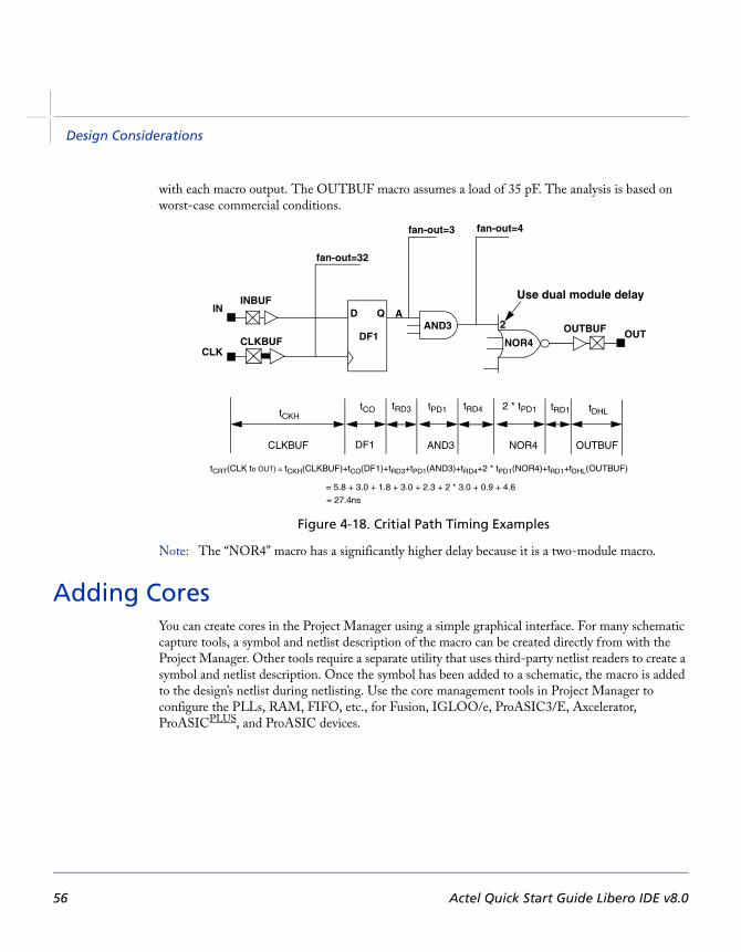
Design Considerations
with each macro output. The OUTBUF macro assumes a load of 35 pF. The analysis is based on worst-case commercial conditions.
Figure 4-18. Critial Path Timing Examples
Note: The “NOR4” macro has a significantly higher delay because it is a two-module macro.
Adding CoresYou can create cores in the Project Manager using a simple graphical interface. For many schematic capture tools, a symbol and netlist description of the macro can be created directly from with the Project Manager. Other tools require a separate utility that uses third-party netlist readers to create a symbol and netlist description. Once the symbol has been added to a schematic, the macro is added to the design’s netlist during netlisting. Use the core management tools in Project Manager to configure the PLLs, RAM, FIFO, etc., for Fusion, IGLOO/e, ProASIC3/E, Axcelerator, ProASICPLUS, and ProASIC devices.
D Q
DF1CLKBUF
INBUFAIN
CLK
fan-out=32
tCKHtCO tPD1 2 * tPD1
AND3
NOR4
2 OUTBUF OUT
tDHL
CLKBUF DF1 AND3 NOR4 OUTBUF
Use dual module delay
tRD3 tRD4 tRD1
tCRT(CLK to OUT) = tCKH(CLKBUF)+tCO(DF1)+tRD3+tPD1(AND3)+tRD4+2 * tPD1(NOR4)+tRD1+tDHL(OUTBUF)
= 5.8 + 3.0 + 1.8 + 3.0 + 2.3 + 2 * 3.0 + 0.9 + 4.6
= 27.4ns
fan-out=3 fan-out=4
56 Actel Quick Start Guide Libero IDE v8.0

AProduct Support
Actel backs its products with various support services including Customer Service, a Customer Technical Support Center, a web site, an FTP site, electronic mail, and worldwide sales offices. This appendix contains information about contacting Actel and using these support services.
Customer ServiceContact Customer Service for non-technical product support, such as product pricing, product upgrades, update information, order status, and authorization.
From Northeast and North Central U.S.A., call 650.318.4480From Southeast and Southwest U.S.A., call 650. 318.4480From South Central U.S.A., call 650.318.4434From Northwest U.S.A., call 650.318.4434From Canada, call 650.318.4480From Europe, call 650.318.4252 or +44 (0)1276.401500From Japan, call 650.318.4743From the rest of the world, call 650.318.4743Fax, from anywhere in the world 650. 318.8044
Actel Customer Technical Support CenterActel staffs its Customer Technical Support Center with highly skilled engineers who can help answer your hardware, software, and design questions. The Customer Technical Support Center spends a great deal of time creating application notes and answers to FAQs. So, before you contact us, please visit our online resources. It is very likely we have already answered your questions.
Actel Technical SupportVisit the Actel Customer Support website (www.actelcom/.custsup/search.html) for more information and support. Many answers available on the searchable web resource include diagrams, illustrations, and links to other resources on the Actel web site.
WebsiteYou can browse a variety of technical and non-technical information on Actel’s home page, at www.actel.com.
Actel Quick Start Guide Libero IDE v8.0 57

Contacting the Customer Technical Support CenterHighly skilled engineers staff the Technical Support Center from 7:00 A.M. to 6:00 P.M., Pacific Time, Monday through Friday. Several ways of contacting the Center follow:
EmailYou can communicate your technical questions to our email address and receive answers back by email, fax, or phone. Also, if you have design problems, you can email your design files to receive assistance. We constantly monitor the email account throughout the day. When sending your request to us, please be sure to include your full name, company name, and your contact information for efficient processing of your request.
The technical support email address is [email protected].
PhoneOur Technical Support Center answers all calls. The center retrieves information, such as your name, company name, phone number and your question, and then issues a case number. The Center then forwards the information to a queue where the first available application engineer receives the data and returns your call. The phone hours are from 7:00 A.M. to 6:00 P.M., Pacific Time, Monday through Friday. The Technical Support numbers are:
650.318.4460800.262.1060
Customers needing assistance outside the US time zones can either contact technical support via email ([email protected]) or contact a local sales office. Sales office listings can be found at www.actel.com/contact/offices/index.html.
58 Actel Quick Start Guide Libero IDE v8.0
IndexIndex
<act_fam> variable 6<vhd_fam> variable 6
AActel 6
Device Families 6Libraries 34web site 57web-based technical support 57
Actel Manuals 6Adding
Global Networks 35Ground 34Pins 50Power 34Properties 47
Adding SmartGen Cores 56ALSPIN 50Assumptions 5Automatic
Fan-In Reduction 38Logic Reduction 38Module Reduction 38Pin Assignment 51
BBack Annotation
Effects of Combiner 42Buffering 37, 45
CCalculating Module Utilization 46Capturing a Design
HDL-Based 18Schematic-Based 16
Checker
checker log 38ChipEditor 12CLK 36CLKA 36CLKB 36Clock
Dedicated 36Routed 36
Combinatorial Module Reduction 38Combiner 38
Back Annotation Effects 42Combining Modules 38
40MX 44ACT 1 44
Compile 10Constant Input Reduction 41Contacting Actel
customer service 57electronic mail 58telephone 58web-based technical support 57
Conventions 6<act_fam> variable 6<vhd_fam> variable 6
Customer service 57
DDCLK 54Dedicated Clocks 36
HCLK 36IOCLK 37
DelayEstimating 55
Design Creation/Verification 18EDIF Netlist Generation 16, 18Functional Simulation 16, 18
Actel Quick Start Guide Libero IDE v8.0 59

Index
HDL Source Entry 18Schematic Capture 16Structural Netlist Generation 19Structural Simulation 19Synthesis 18
Design FlowDesign Creation/Verification 18Design Implementation 16Schematic-Based 15–??Synthesis-Based ??–19
Design Implementation 16Place-and-Route 17Power Analysis 17Timing Simulation 17
Design Layout 17Design Synthesis 18Designer
Overview 7–13Place-and-Route 17Timing Analysis 17
Designer Maintenance 13Designs
Hierarchical 34Multiple Sheet 34
DeviceFamilies 6Programming 17Verification 19
Document Assumptions 5Document Conventions 6Document Organization 5Duplicating Logic 45
EEDIF Netlist Generation
Schematic-Based 16
Synthesis-Based 18Electronic mail 58Estimating Delays 55
FFan Out 45Fan-In Reduction 38, 42Functional Simulation 16, 18Fuse 11
GGate-Level Netlist 18Generating 55
EDIF Netlist 16, 18Gate-Level Netlist 18Structural Netlist 19
Global Network 35GND 34Ground 34
HHCLK 36HDL Source Entry 18Hierarchical
Designs 34High Fan Out 45High fan-out signals 38
II/O
Clock 37Module Utilization 46
IOCLK 37IOPCL 37
60 Actel Quick Start Guide Libero IDE v8.0
Index
JJTAG Pins 54
LLayout 10
Standard 10Timing Driven 10
Libraries 34Logic Module Utilization 46Logic Reduction 38, 41
MMaintenance Mode 13Manual Pin Assignment 51Module Reduction 38
40MX 44ACT 1 44Combinatorial 38
Multiple Sheet Designs 34
NNaming Conventions
Schematic 31Verilog 32VHDL 31
NetLoading 45
Netlist GenerationEDIF 16, 18Gate-Level 18Structural 19
Network 35
OOnline Help 6
PPin
Adding 50Assignment 50–54Automatic Assignment 51DCLK 54JTAG 54PRA 54PRB 54Probe 54SDI 54TCK 54TDI 54TDO 54TMS 54Unused I/O 54
PinEditor 12Place-and-Route 17Power 34Power Analysis 17PRA 54PRB 54Preserving Macros 47ProASIC
global routing resources 37Probe Pins 54Product Support 57–58Product support
customer service 57electronic mail 58technical support 57web site 57
Programming a Device 17Property, ALSPRESERVE 47
Actel Quick Start Guide Libero IDE v8.0 61

Index
RRemapping 39Routed Clocks 36
CLK 36CLKA 36CLKB 36QCLK 36
SSchematic Capture 16Schematic-Based Design Flow 15–??
Design Implementation 16Programming 17
SDI 54Sequential Remapping 39Simulation
Functional 16, 18Schematic-Based 16, 17Structural 19Synthesis-Based 18, 19Timing 17
SmartGen Core Builder 56SmartPower 17Special Clocks 37
IOPCL 37Static Timing Analysis 17Structural Netlist Generation 19Structural Simulation 19Symbol, Top Level 55Synthesis 18Synthesis-Based Design Flow ??–19
Design Creation/Verification 18
System Verification 19System Verification 19
Silicon Explorer II 19
TTCK 54TDI 54TDO 54Timer 12Timer Tool 17Timing 10Timing Analysis 17Timing Constraint 55Timing Simulation 17TMS 54Top Level Symbol 55
UUnit Delays 16, 18Unused Logic Removal 41Utilization 46
Vvariables
<act_fam> 6<vhd_fam> 6
VCC 34
WWeb-based technical support 57
62 Actel Quick Start Guide Libero IDE v8.0


For more information about Actel’s products, visit our website at http://www.actel.comActel Corporation • 2061 Stierlin Court • Mountain View, CA 94043 USACustomer Service: 650.318.1010 • Customer Applications Center: 800.262.1060
Actel Europe Ltd. • River Court, Meadows Business Park, Station Approach • Blackwater, Surrey GU17 9AB • United Kingdom
Phone +44 (0) 1276 609 300 • Fax +44 (0) 1276 607 540
Actel Japan • EXOS Ebisu Bldg. 4F • 1-24-14 Ebisu Shibuya-ku • Tokyo 150 • JapanPhone +81.03.3445.7671 • Fax +81.03.3445.7668 • www.jp.actel.com
Actel Hong Kong • Suite 2114, Two Pacific Place • 88 Queensway, Admiralty Hong Kong
Phone +852 2185 6460 • Fax +852 2185 6488 • www.actel.com.cn
5-02-9123-13 06.07