Embed Size (px)
Citation preview
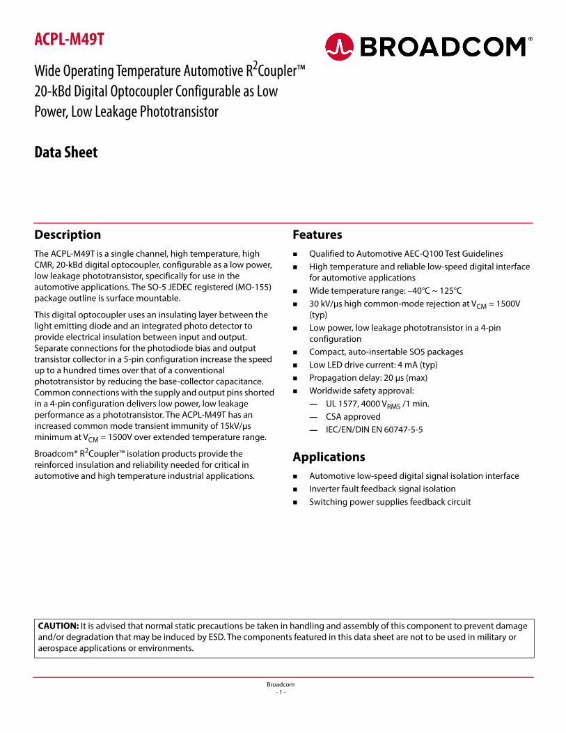
ACPL-M49T
Wide Operating Temperature Automotive R2Coupler™ 20-kBd Digital Optocoupler Configurable as Low Power, Low Leakage Phototransistor
Data Sheet
DescriptionThe ACPL-M49T is a single channel, high temperature, high CMR, 20-kBd digital optocoupler, configurable as a low power, low leakage phototransistor, specifically for use in the automotive applications. The SO-5 JEDEC registered (MO-155) package outline is surface mountable.
This digital optocoupler uses an insulating layer between the light emitting diode and an integrated photo detector to provide electrical insulation between input and output. Separate connections for the photodiode bias and output transistor collector in a 5-pin configuration increase the speed up to a hundred times over that of a conventional phototransistor by reducing the base-collector capacitance. Common connections with the supply and output pins shorted in a 4-pin configuration delivers low power, low leakage performance as a phototransistor. The ACPL-M49T has an increased common mode transient immunity of 15kV/μs minimum at VCM = 1500V over extended temperature range.
Broadcom® R2Coupler™ isolation products provide the reinforced insulation and reliability needed for critical in automotive and high temperature industrial applications.
Features Qualified to Automotive AEC-Q100 Test Guidelines High temperature and reliable low-speed digital interface
for automotive applications Wide temperature range: –40°C ~ 125°C 30 kV/μs high common-mode rejection at VCM = 1500V
(typ) Low power, low leakage phototransistor in a 4-pin
configuration Compact, auto-insertable SO5 packages Low LED drive current: 4 mA (typ) Propagation delay: 20 μs (max) Worldwide safety approval:
— UL 1577, 4000 VRMS /1 min. — CSA approved— IEC/EN/DIN EN 60747-5-5
Applications Automotive low-speed digital signal isolation interface Inverter fault feedback signal isolation Switching power supplies feedback circuit
CAUTION: It is advised that normal static precautions be taken in handling and assembly of this component to prevent damage and/or degradation that may be induced by ESD. The components featured in this data sheet are not to be used in military or aerospace applications or environments.
Broadcom- 1 -
ACPL-M49T Data Sheet
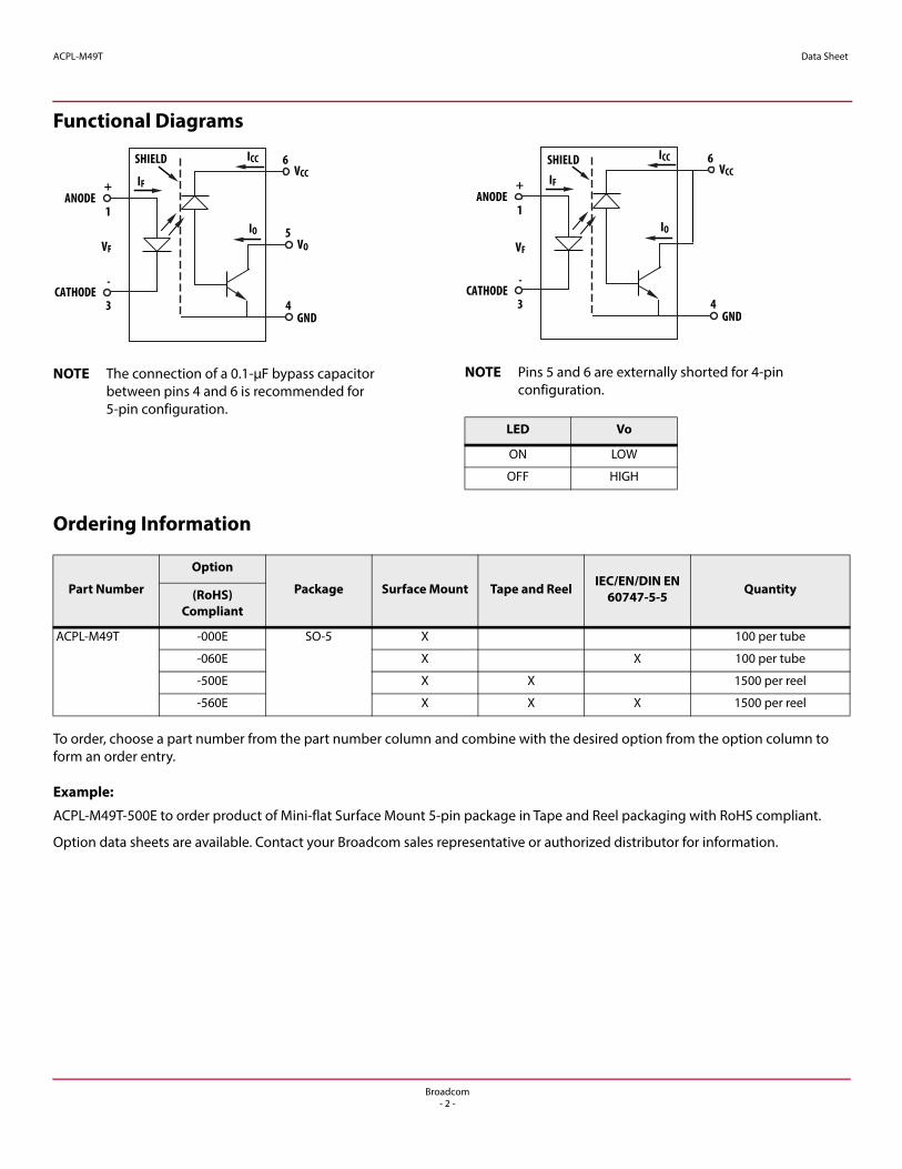
Functional Diagrams
NOTE The connection of a 0.1-μF bypass capacitor between pins 4 and 6 is recommended for 5-pin configuration.
NOTE Pins 5 and 6 are externally shorted for 4-pin configuration.
IF
SHIELD 6
5
4GND
VCC
1
3
VO
ICC
VF
IO
ANODE
CATHODE
+
-
LED Vo
ON LOW
OFF HIGH
IF
SHIELD 6
4GND
VCC
1
3
ICC
VF
IO
ANODE
CATHODE
+
-
Ordering Information
To order, choose a part number from the part number column and combine with the desired option from the option column to form an order entry.
Example:
ACPL-M49T-500E to order product of Mini-flat Surface Mount 5-pin package in Tape and Reel packaging with RoHS compliant.
Option data sheets are available. Contact your Broadcom sales representative or authorized distributor for information.
Part Number
Option
Package Surface Mount Tape and Reel IEC/EN/DIN EN 60747-5-5 Quantity(RoHS)
Compliant
ACPL-M49T -000E SO-5 X 100 per tube
-060E X X 100 per tube
-500E X X 1500 per reel
-560E X X X 1500 per reel
Broadcom- 2 -
ACPL-M49T Data Sheet
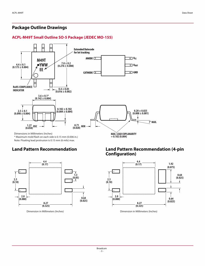
Package Outline Drawings
ACPL-M49T Small Outline SO-5 Package (JEDEC MO-155)
M49T YWW
EE7.0 ± 0.2
(0.276 ± 0.008)
2.5 ± 0.1(0.098 ± 0.004)
0.102 ± 0.102(0.004 ± 0.004)
4.4 ± 0.1(0.173 ± 0.004)
1.27(0.050) BSC
0.20 ± 0.025(0.008 ± 0.001)
0.71(0.028) MIN
0.4 ± 0.05(0.016 ± 0.002)
3.6 ± 0.1*(0.142 ± 0.004)
Dimensions in Millimeters (Inches)* Maximum mold flash on each side is 0.15 mm (0.006 in.)Note: Floating lead protrusion is 0.15 mm (6 mils) max.
7° MAX.
MAX. LEAD COPLANARITY= 0.102 (0.004)
6
5
43
1 VCC
VOUT
GNDCATHODE
ANODE
Extended Datecode for lot tracking
RoHS-COMPLIANCEINDICATOR
Land Pattern Recommendation Land Pattern Recommendation (4-pin Configuration)
8.27(0.325)
2.0(0.080)
2.5(0.10)
1.3(0.05)
0.64(0.025)
4.4(0.17)
Dimension in Millimeters (Inches)
8.27(0.325)
2.0(0.080)
2.5(0.10)
1.92(0.075)
0.64(0.025)
4.4(0.17)
Dimension in Millimeters (Inches)
0.64(0.025)
Broadcom- 3 -
ACPL-M49T Data Sheet
Recommended Pb-Free IR ProfileRecommended reflow condition as per JEDEC Standard, J-STD-020 (latest revision).
NOTE Non-halide flux should be used.
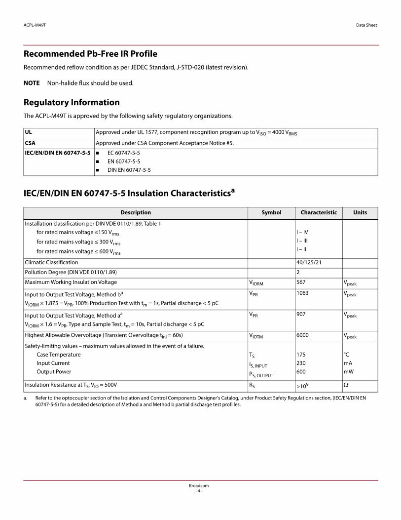
Regulatory InformationThe ACPL-M49T is approved by the following safety regulatory organizations.
IEC/EN/DIN EN 60747-5-5 Insulation Characteristicsa
UL Approved under UL 1577, component recognition program up to VISO = 4000 VRMS
CSA Approved under CSA Component Acceptance Notice #5.
IEC/EN/DIN EN 60747-5-5 EC 60747-5-5 EN 60747-5-5 DIN EN 60747-5-5
Description Symbol Characteristic Units
Installation classification per DIN VDE 0110/1.89, Table 1for rated mains voltage ≤150 Vrms
for rated mains voltage ≤ 300 Vrms
for rated mains voltage ≤ 600 Vrms
I – IVI – IIII – II
Climatic Classification 40/125/21
Pollution Degree (DIN VDE 0110/1.89) 2
Maximum Working Insulation Voltage VIORM 567 Vpeak
Input to Output Test Voltage, Method ba
VIORM × 1.875 = VPR, 100% Production Test with tm = 1s, Partial discharge < 5 pC
a. Refer to the optocoupler section of the Isolation and Control Components Designer’s Catalog, under Product Safety Regulations section, (IEC/EN/DIN EN 60747-5-5) for a detailed description of Method a and Method b partial discharge test profi les.
VPR 1063 Vpeak
Input to Output Test Voltage, Method aa VIORM × 1.6 = VPR, Type and Sample Test, tm = 10s, Partial discharge < 5 pC
VPR 907 Vpeak
Highest Allowable Overvoltage (Transient Overvoltage tini = 60s) VIOTM 6000 Vpeak
Safety-limiting values – maximum values allowed in the event of a failure.Case TemperatureInput CurrentOutput Power
TS
IS, INPUT
PS, OUTPUT
175 230 600
°CmAmW
Insulation Resistance at TS, VIO = 500V RS >109
Broadcom- 4 -
ACPL-M49T Data Sheet
Insulation and Safety-Related Specifications
Absolute Maximum Ratings
Recommended Operating Conditions
Parameter Symbol ACPL-M49T Units Conditions
Minimum External Air Gap (Clearance) L(101) ≥ 5 mm Measured from input terminals to output terminals, shortest distance through air.
Minimum External Tracking (Creepage) L(102) ≥ 5 mm Measured from input terminals to output terminals, shortest distance path along body.
Minimum Internal Plastic Gap (Internal Clearance)
0.08 mm Through insulation distance conductor to conductor, usually the straight line distance thickness between the emitter and detector.
Tracking Resistance (Comparative Tracking Index)
CTI 175 V DIN IEC 112/VDE 0303 Part 1
Isolation Group (DIN VDE0109) IIIa Material Group (DIN VDE 0109)
Parameter Symbol Min. Max. Units Note
Storage Temperature TS –55 150 °C
Operating Temperature TA –40 125 °C
Lead Soldering Cycle Temperature — 260 °C
Time — 10 s
Average Forward Input Current IF(avg) — 20 mA a
a. Derate linearly above 85°C free-air temperature at a rate of 0.25 mA/°C.
Peak Forward Input Current 50% duty cycle, 1-ms pulse width) IF(peak) — 40 mA b
b. Derate linearly above 85°C free-air temperature at a rate of 0.30 mA/°C.
Peak Transient Input Current (≤1-μs pulse width, 300 ps) IF(trans) — 100 mA b
Reversed Input Voltage VR — 5 V Pin 3 - 1
Input Power Dissipation PIN — 30 mW c
c. Derate linearly above 85°C free-air temperature at a rate of 0.375 mW/°C.
Output Power Dissipation PO — 100 mW d
d. Derate linearly above 85°C free-air temperature at a rate of 1.875 mW/°C.
Average Output Current IO — 8 mA
Peak Output Current Io(pk) — 16 mA
Supply Voltage (Pins 6–4) VCC –0.5 30 V
Output Voltage (Pins 5–4) VO –0.5 20 V
Solder Reflow Temperature Profile See Reflow Temperature Profile
Parameter Symbol Min. Max. Units Note
Supply Voltage VCC — 20.0 V
Operating Temperature TA –40 125 °C
Broadcom- 5 -
ACPL-M49T Data Sheet
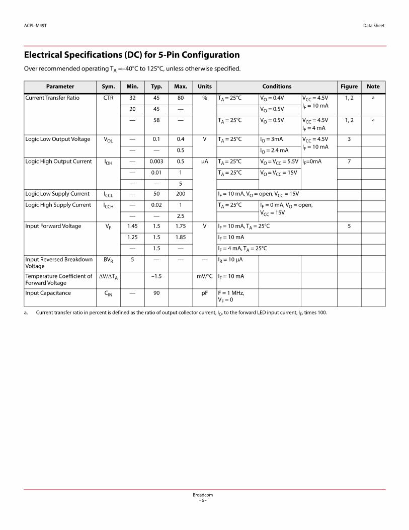
Electrical Specifications (DC) for 5-Pin ConfigurationOver recommended operating TA =–40°C to 125°C, unless otherwise specified.
Parameter Sym. Min. Typ. Max. Units Conditions Figure Note
Current Transfer Ratio CTR 32 45 80 % TA = 25°C VO = 0.4V VCC = 4.5V IF = 10 mA
1, 2 a
a. Current transfer ratio in percent is defined as the ratio of output collector current, IO, to the forward LED input current, IF, times 100.
20 45 — VO = 0.5V
— 58 — TA = 25°C VO = 0.5V VCC = 4.5V IF = 4 mA
1, 2 a
Logic Low Output Voltage VOL — 0.1 0.4 V TA = 25°C IO = 3mA VCC = 4.5V IF = 10 mA
3
— — 0.5 IO = 2.4 mA
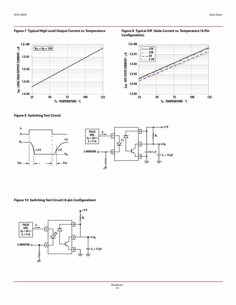
Logic High Output Current IOH — 0.003 0.5 μA TA = 25°C VO = VCC = 5.5V IF=0mA 7
— 0.01 1 TA = 25°C VO = VCC = 15V
— — 5
Logic Low Supply Current ICCL — 50 200 IF = 10 mA, VO = open, VCC = 15V
Logic High Supply Current ICCH — 0.02 1 TA = 25°C IF = 0 mA, VO = open, VCC = 15V— — 2.5
Input Forward Voltage VF 1.45 1.5 1.75 V IF = 10 mA, TA = 25°C 5
1.25 1.5 1.85 IF = 10 mA
— 1.5 — IF = 4 mA, TA = 25°C
Input Reversed Breakdown Voltage
BVR 5 — — — IR = 10 μA
Temperature Coefficient of Forward Voltage
V/TA –1.5 mV/°C IF = 10 mA
Input Capacitance CIN — 90 pF F = 1 MHz, VF = 0
Broadcom- 6 -
ACPL-M49T Data Sheet
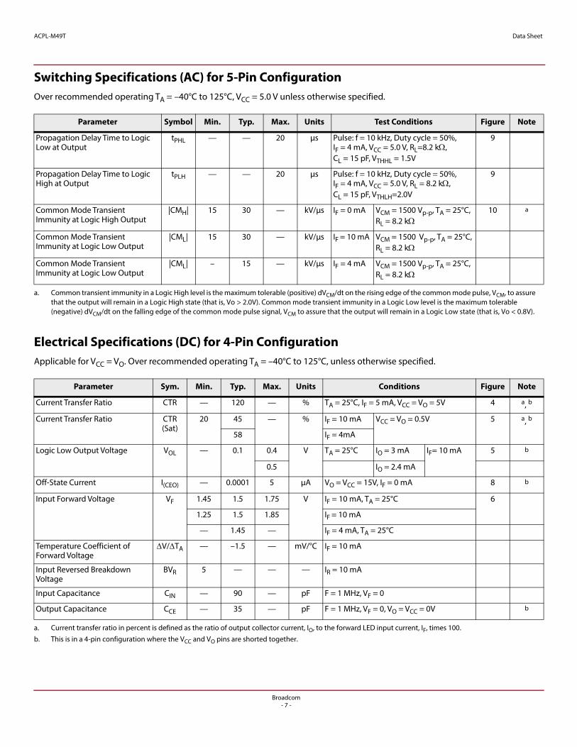
Switching Specifications (AC) for 5-Pin ConfigurationOver recommended operating TA = –40°C to 125°C, VCC = 5.0 V unless otherwise specified.
Electrical Specifications (DC) for 4-Pin ConfigurationApplicable for VCC = VO. Over recommended operating TA = –40°C to 125°C, unless otherwise specified.
Parameter Symbol Min. Typ. Max. Units Test Conditions Figure Note
Propagation Delay Time to Logic Low at Output
tPHL — — 20 μs Pulse: f = 10 kHz, Duty cycle = 50%, IF = 4 mA, VCC = 5.0 V, RL=8.2 k, CL = 15 pF, VTHHL = 1.5V
9
Propagation Delay Time to Logic High at Output
tPLH — — 20 μs Pulse: f = 10 kHz, Duty cycle = 50%, IF = 4 mA, VCC = 5.0 V, RL = 8.2 k, CL = 15 pF, VTHLH=2.0V
9
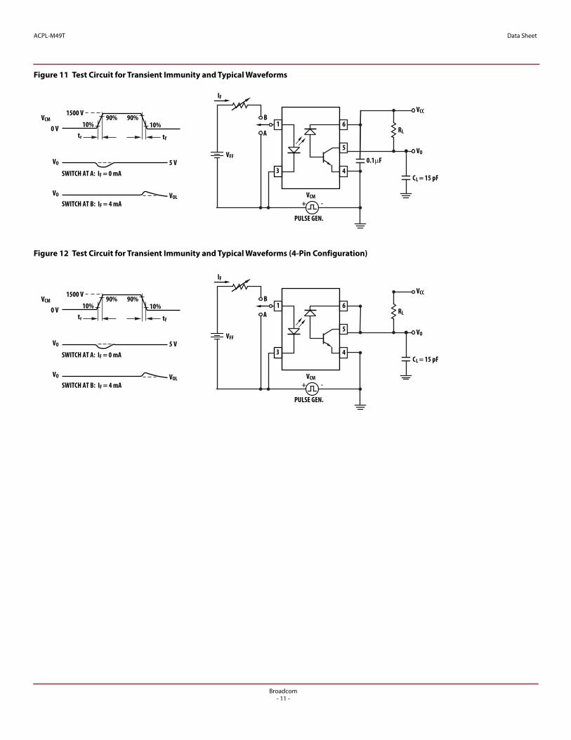
Common Mode Transient Immunity at Logic High Output
|CMH| 15 30 — kV/μs IF = 0 mA VCM = 1500 Vp-p, TA = 25°C, RL = 8.2 k
10 a
a. Common transient immunity in a Logic High level is the maximum tolerable (positive) dVCM/dt on the rising edge of the common mode pulse, VCM, to assure that the output will remain in a Logic High state (that is, Vo > 2.0V). Common mode transient immunity in a Logic Low level is the maximum tolerable (negative) dVCM/dt on the falling edge of the common mode pulse signal, VCM to assure that the output will remain in a Logic Low state (that is, Vo < 0.8V).
Common Mode Transient Immunity at Logic Low Output
|CML| 15 30 — kV/μs IF = 10 mA VCM = 1500 Vp-p, TA = 25°C, RL = 8.2 k
Common Mode Transient Immunity at Logic Low Output
|CML| – 15 — kV/μs IF = 4 mA VCM = 1500 Vp-p, TA = 25°C, RL = 8.2 k
Parameter Sym. Min. Typ. Max. Units Conditions Figure Note
Current Transfer Ratio CTR — 120 — % TA = 25°C, IF = 5 mA, VCC = VO = 5V 4 a, b
a. Current transfer ratio in percent is defined as the ratio of output collector current, IO, to the forward LED input current, IF, times 100.
b. This is in a 4-pin configuration where the VCC and VO pins are shorted together.
Current Transfer Ratio CTR (Sat)
20 45 — % IF = 10 mA VCC = VO = 0.5V 5 a, b
58 IF = 4mA
Logic Low Output Voltage VOL — 0.1 0.4 V TA = 25°C IO = 3 mA IF= 10 mA 5 b
0.5 IO = 2.4 mA
Off-State Current I(CEO) — 0.0001 5 μA VO = VCC = 15V, IF = 0 mA 8 b
Input Forward Voltage VF 1.45 1.5 1.75 V IF = 10 mA, TA = 25°C 6
1.25 1.5 1.85 IF = 10 mA
— 1.45 — IF = 4 mA, TA = 25°C
Temperature Coefficient of Forward Voltage
V/TA — –1.5 — mV/°C IF = 10 mA
Input Reversed Breakdown Voltage
BVR 5 — — — IR = 10 mA
Input Capacitance CIN — 90 — pF F = 1 MHz, VF = 0
Output Capacitance CCE — 35 — pF F = 1 MHz, VF = 0, VO = VCC = 0V b
Broadcom- 7 -
ACPL-M49T Data Sheet
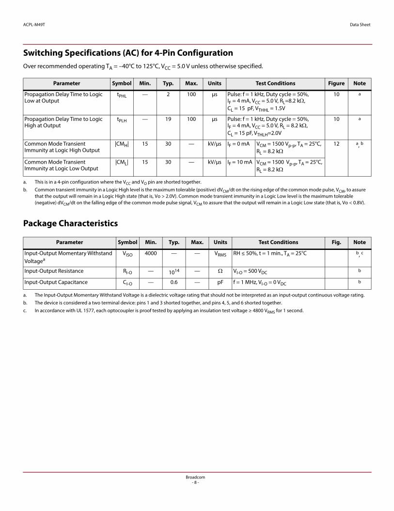
Switching Specifications (AC) for 4-Pin ConfigurationOver recommended operating TA = –40°C to 125°C, VCC = 5.0 V unless otherwise specified.
Package Characteristics
Parameter Symbol Min. Typ. Max. Units Test Conditions Figure Note
Propagation Delay Time to Logic Low at Output
tPHL — 2 100 μs Pulse: f = 1 kHz, Duty cycle = 50%, IF = 4 mA, VCC = 5.0 V, RL=8.2 k, CL = 15 pF, VTHHL = 1.5V
10 a
a. This is in a 4-pin configuration where the VCC and VO pin are shorted together.
Propagation Delay Time to Logic High at Output
tPLH — 19 100 μs Pulse: f = 1 kHz, Duty cycle = 50%, IF = 4 mA, VCC = 5.0 V, RL = 8.2 k, CL = 15 pF, VTHLH=2.0V
10 a
Common Mode Transient Immunity at Logic High Output
|CMH| 15 30 — kV/μs IF = 0 mA VCM = 1500 Vp-p, TA = 25°C, RL = 8.2 k
12 a, b
b. Common transient immunity in a Logic High level is the maximum tolerable (positive) dVCM/dt on the rising edge of the common mode pulse, VCM, to assure that the output will remain in a Logic High state (that is, Vo > 2.0V). Common mode transient immunity in a Logic Low level is the maximum tolerable (negative) dVCM/dt on the falling edge of the common mode pulse signal, VCM to assure that the output will remain in a Logic Low state (that is, Vo < 0.8V).
Common Mode Transient Immunity at Logic Low Output
|CML| 15 30 — kV/μs IF = 10 mA VCM = 1500 Vp-p, TA = 25°C, RL = 8.2 k
Parameter Symbol Min. Typ. Max. Units Test Conditions Fig. Note
Input-Output Momentary Withstand Voltagea
a. The Input-Output Momentary Withstand Voltage is a dielectric voltage rating that should not be interpreted as an input-output continuous voltage rating.
VISO 4000 — — VRMS RH ≤ 50%, t = 1 min., TA = 25°C b, c
b. The device is considered a two terminal device: pins 1 and 3 shorted together, and pins 4, 5, and 6 shorted together.
c. In accordance with UL 1577, each optocoupler is proof tested by applying an insulation test voltage ≥ 4800 VRMS for 1 second.
Input-Output Resistance RI-O — 1014 — VI-O = 500 VDC b
Input-Output Capacitance CI-O — 0.6 — pF f = 1 MHz, VI-O = 0 VDC b
Broadcom- 8 -
ACPL-M49T Data Sheet
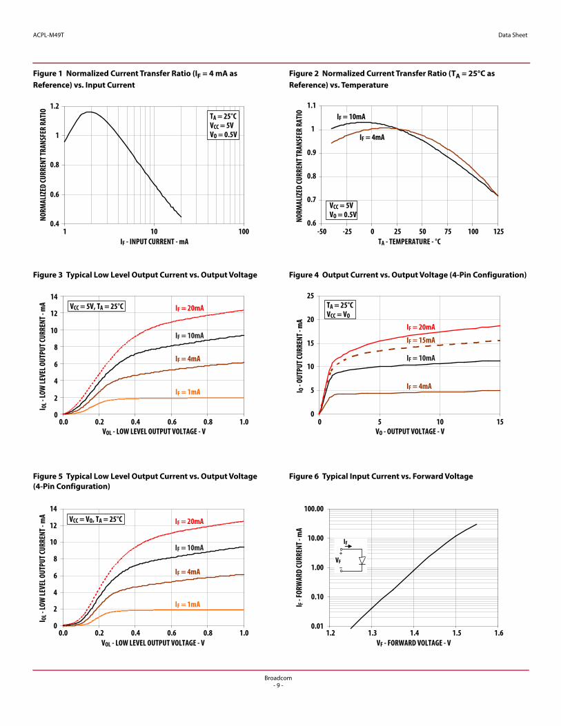
Figure 1 Normalized Current Transfer Ratio (IF = 4 mA as Reference) vs. Input Current
Figure 2 Normalized Current Transfer Ratio (TA = 25°C as Reference) vs. Temperature
0.4
0.6
0.8
1
1.2
1 10 100
NORM
ALIZ
ED CU
RREN
T TRA
NSFE
R RA
TIO
IF - INPUT CURRENT - mA
TA = 25°CVCC = 5VVO = 0.5V
TA - TEMPERATURE - °C
0.6
0.7
0.8
0.9
1
1.1
-50 -25 0 25 50 75 100 125
NORM
ALIZ
ED CU
RREN
T TRA
NSFE
R RA
TIO
IF = 10mA
IF = 4mA
VCC = 5VVO = 0.5V
Figure 3 Typical Low Level Output Current vs. Output Voltage Figure 4 Output Current vs. Output Voltage (4-Pin Configuration)
VOL - LOW LEVEL OUTPUT VOLTAGE - V
I OL -
LOW
LEVE
L OUT
PUT C
URRE
NT - m
A
0
2
4
6
8
10
12
14
0.0 0.2 0.4 0.6 0.8 1.0
VCC = 5V, TA = 25°C IF = 20mA
IF = 10mA
IF = 4mA
IF = 1mA
0
5
10
15
20
25
0 5 10 15
I O - O
UTPU
T CUR
RENT
- mA
VO - OUTPUT VOLTAGE - V
TA = 25°CVCC = VO
IF = 20mA
IF = 10mA
IF = 15mA
IF = 4mA
Figure 5 Typical Low Level Output Current vs. Output Voltage (4-Pin Configuration)
Figure 6 Typical Input Current vs. Forward Voltage
0
2
4
6
8
10
12
14
0.0 0.2 0.4 0.6 0.8 1.0VOL - LOW LEVEL OUTPUT VOLTAGE - V
I OL -
LOW
LEVE
L OUT
PUT C
URRE
NT - m
A
IF = 20mA
IF = 10mA
IF = 4mA
IF = 1mA
VCC = VO, TA = 25°C
VF - FORWARD VOLTAGE - V
I F - F
ORW
ARD
CURR
ENT -
mA
0.01
0.10
1.00
10.00
100.00
1.2 1.3 1.4 1.5 1.6
IF
VF
+
–
Broadcom- 9 -
ACPL-M49T Data Sheet
Figure 7 Typical High Level Output Current vs. Temperature Figure 8 Typical Off -State Current vs. Temperature (4-Pin Configuration)
1.E-04
1.E-03
1.E-02
1.E-01
1.E+00
25 50 75 100 125
I OH -
LOGI
C HIG
H OU
TPUT
CURR
ENT -
A
TA - TEMPERATURE - °C
VCC = VO = 15V
1.E-05
1.E-04
1.E-03
1.E-02
1.E-01
1.E+00
25 50 75 100 125
I CEO -
OFF
-STA
TE CU
RREN
T -
A
TA - TEMPERATURE - °C
15V12V5V3.3V
Figure 9 Switching Test Circuit
VO
PULSEGEN.
ZO = 50 tr = 5 ns
IF MONITOR
IF
0.1 F
RL
CL = 15 pF
0
tPHL tPLH
VO
IF
VOL
1.5 V
1
3
6
5
4
2 V
5 V
+5 V
Figure 10 Switching Test Circuit (4-pin Configuration)
VO
C = 15 pFL
PULSEGEN.
ZO = 50 tr = 5 ns
IF MONITOR
IF
RL
1
3
6
5
4
+5 V
Broadcom- 10 -
ACPL-M49T Data Sheet
Figure 11 Test Circuit for Transient Immunity and Typical Waveforms
Figure 12 Test Circuit for Transient Immunity and Typical Waveforms (4-Pin Configuration)
VO
C = 15 pFL
IF
RLA
B
PULSE GEN.
VCM+
VFFVO
VOLVO
0 V 10%90% 90%
10%
SWITCH AT A: IF = 0 mA
SWITCH AT B: IF = 4 mA
VCM
tr tf
5 V
VCC
-
1500 V1
3
6
5
40.1 F
VO
C = 15 pFL
IF
RLA
B
PULSE GEN.
VCM+
VFFVO
VOLVO
0 V 10%90% 90%
10%
SWITCH AT A: IF = 0 mA
SWITCH AT B: IF = 4 mA
VCM
tr tf
5 V
VCC
-
1500 V1
3
6
5
4
Broadcom- 11 -

For product information and a complete list of distributors, please go to our web site: www.broadcom.com.
Broadcom, the pulse logo, Connecting everything, Avago Technologies, Avago, the A logo, and R2Coupler are among the trademarks of Broadcom and/or its affiliates in the United States, certain other countries and/or the EU.
Copyright © 2011–2017 by Broadcom. All Rights Reserved.
The term "Broadcom" refers to Broadcom Limited and/or its subsidiaries. For more information, please visit www.broadcom.com.
Broadcom reserves the right to make changes without further notice to any products or data herein to improve reliability, function, or design.
Information furnished by Broadcom is believed to be accurate and reliable. However, Broadcom does not assume any liability arising out of the application or use of this information, nor the application or use of any product or circuit described herein, neither does it convey any license under its patent rights nor the rights of others.
AV02-2373EN – July 10, 2017