Embed Size (px)
Citation preview
i
Acknowledgements I would like to thank Professor Rogers for being very generous with his time during the
course of this project. His assistance did much to ensure its successful completion. I
would also like to thank my fellow group members: Kevin Cheung; Derek van Gaal;
Christina George; Vincent Karam and Bi Pham, who were always eager to offer
assistance; and with whom it was a pleasure to work. As well, Stephen Knox’s tutorial
on layout in Cadence Virtuoso was greatly appreciated.

ii
Executive Summary The following is a report on the design of a frequency synthesizer for a cable tuner. The
synthesizer provides the mixers with the local oscillator (LO). This report specifically
deals with the phase-frequency detector (PFD) and charge pump, with an exploratory
look at the divide-by-two. In addition to schematic design, the PFD and charge pump
were laid out. These layouts were again simulated.
Design began with the PFD. The PFD takes phase errors and quantizes them into voltage
pulses. It was built from logic gates that were each individually designed and tested. It
was successfully tested for both phase errors and frequency errors and was found to have
a phase constant, Kphase = 1 V/Hz. Post layout simulations gave the same results.
The charge pump takes the PFD voltage pulses and translates them into currents. It
consists of two current sources controlled by each output of the PFD. Testing of the
design showed charge UP current of 2.38 mA and a charge DOWN current of 2.35 mA, a
mismatch of 1.27%. Post layout simulations showed the current mismatch increased to
4.9% (UP = 2.283 mA, DOWN = 2.397 mA)
The divide-by-two was implemented as two latches connected to make a flip-flop. The
latches were first tested individually at 2 GHz, then combined as a flip-flop in an inverted
feedback loop. The divider functioned properly: With a 2 GHz input the output was 1
GHz, with a 50% duty cycle.
The components were assembled into a phase-locked loop (PLL) testbench, which
included a low pass filter and ideal VCO. The synthesizer functioned successfully. The

iii
VCO output settled at 8 MHz, twice the 4 MHz input, in 26µs for both schematic and
extracted layout simulations.
Periodic Noise simulations revealed phase noise of -121 dBc/Hz and output noise of
-187.3 dB for the schematic. Post layout phase noise was -113 dBc/Hz and output noise
was -174.4 dB.

iv
Table of Contents List of Figures ..................................................................................................................... v List of Tables....................................................................................................................... v 1.0 Introduction ............................................................................................................. 6 2.0 Objective ................................................................................................................. 7 3.0 Motivation ............................................................................................................... 7 4.0 Theory and Design .................................................................................................. 8
4.1 Basic Digital Building Blocks............................................................................. 9 4.1.1 The Inverter ................................................................................................. 9 4.1.2 The NAND and NOR Gates...................................................................... 12
4.2 Phase/Frequency Detector................................................................................ 15 4.2.1 Background ............................................................................................... 15 4.2.2 Circuit........................................................................................................ 16 4.2.3 Simulation and Results.............................................................................. 17
4.3 Charge Pump.................................................................................................... 19 4.3.1 Background ............................................................................................... 19 4.3.2 Circuit........................................................................................................ 20 4.3.3 Simulation and Results.............................................................................. 21
4.4 Frequency Divide-by-two ................................................................................ 22 4.4.1 Background ............................................................................................... 22 4.4.2 Circuit........................................................................................................ 22 4.4.3 Simulation and Results.............................................................................. 23
4.5 Phase-Locked Loop........................................................................................... 24 4.5.1 Circuit Overview....................................................................................... 24 4.5.2 Design........................................................................................................ 25 4.5.3 Simulation and Results.............................................................................. 26
5.0 Layout.................................................................................................................... 29 5.1 Inverter .............................................................................................................. 29 5.2 NAND Gate....................................................................................................... 31 5.3 NOR Gate.......................................................................................................... 32 5.4 Phase/Frequency Detector................................................................................. 34 5.4 Charge Pump..................................................................................................... 36 5.5 PLL.................................................................................................................... 38
6.0 Conclusions ........................................................................................................... 40 7.0 Future Work and Recommendations..................................................................... 42 8.0 References ............................................................................................................. 43

v
List of Figures Figure 1: System Diagram of CMOS Cable Tuner [1] ....................................................... 7 Figure 2: Frequency Synthesizer System Diagram [1] ....................................................... 8 Figure 3: CMOS Inverter .................................................................................................. 10 Figure 4: Transient Simulation of Inverter; a) Input; b) Output ....................................... 11 Figure 5: a) NAND gate; b) NOR gate ............................................................................. 12 Figure 6: Inverter Modeled by Drain-Source Resistances [2]........................................... 13 Figure 7: Transient Simulation of NAND and NOR Gates .............................................. 15 Figure 8: a) PFD State Table [3]; b) Example output of state table.................................. 15 Figure 9: a) PFD Block circuit [3]; c) D-Flip Flop Circuit [3] ......................................... 17 Figure 10: Transient Simulation of PFD: a) Phase Error; b) Frequency Error ................. 18 Figure 11: Conceptual Charge Pump Circuit [3] .............................................................. 20 Figure 12: Charge Pump Circuit ....................................................................................... 21 Figure 13: Frequency Divide-by-two Block Diagram [4]................................................. 22 Figure 14: Latch circuit ..................................................................................................... 23 Figure 15: Transient Simulation of Latch ......................................................................... 24 Figure 16: Transient Simulation of Divide-by-Two ......................................................... 24 Figure 17: PLL Test bench................................................................................................ 25 Figure 18: Transient Simulation of PLL Test bench......................................................... 27 Figure 19: Periodic Noise Simulation: a) Phase Noise; b) Output Noise ......................... 28 Figure 20: Inverter Layout ................................................................................................ 30 Figure 21: Inverter Post Layout Simulation...................................................................... 30 Figure 22: NAND Gate Layout......................................................................................... 31 Figure 23: NAND Gate Post Layout Simulations............................................................. 32 Figure 24: NOR Gate Layout ............................................................................................ 33 Figure 25: NOR Gate Post Layout Simulation.................................................................. 33 Figure 26: D Flip Flop Layout .......................................................................................... 34 Figure 27: PFD Layout...................................................................................................... 35 Figure 28: Post Layout Simulation for PFD...................................................................... 35 Figure 29: Charge-Pump Layout....................................................................................... 37 Figure 30: PLL Post-Layout Simulation ........................................................................... 38 Figure 31: PLL Post-Layout Periodic Noise Simulations: a) Phase Noise; b) Output Noise
................................................................................................................................... 39
List of Tables Table 1: Synthesizer Specifications .................................................................................... 9

6
1.0 Introduction This project is the design of a CMOS (Complementary Metal Oxide Semiconductor)
cable tuner for the DOCSIS (Data-Over-Cable Service Interface Specifications) market.
A system level schematic is shown in figure 1.
The overall system specifications for the tuner are: Input Range = 47-870 MHz; composite
second-order beat (CSO) and composite triple-order beat (CTB) <= 50 dBc at 15 dBmV;
noise figure (NF) = 9 dB.
This is a 6 member group project. The tuner components have been divided up with each
group member responsible for a specific block. The following are the group members and
their respective block: Kevin Cheung is designing the voltage controlled oscillator (VCO);
Christina George is designing the low noise amplifier (LNA); Vincent Karam is designing
the mixer in the image reject mixer (IMR); Derek van Gaal is designing the additional
circuitry to complement the IMR; Bi Pham is designing the first mixer and I am designing
the phase/frequency detector with charge pump for the second frequency synthesizer.
Professor Rogers is the project supervisor.

7
Figure 1: System Diagram of CMOS Cable Tuner [1]
2.0 Objective
My objective is to design and test a phase/frequency detector and charge pump to meet the
given specifications. I will also take an exploratory look at the divide-by-two.
Complementary to the technical work, I plan to also get an insight into integrated circuit
design, telecommunications circuitry, and working on an engineering project in a team
environment.
3.0 Motivation Recently in the electronics industry there has been increasing emphasis on integrated
design solutions. Application specific integrated circuits (ASICs) are in demand. For
this reason I thought it would be interesting to look at integrated circuit (IC) design for
my fourth year project. The CMOS cable tuner project seemed like an excellent
opportunity to explore this field. When it came to choosing a component of the tuner, I
felt the most interesting would be the synthesizer as it combines both analogue and digital
circuits.

8
4.0 Theory and Design The second frequency synthesizer uses a phase-locked loop (PLL) to generate the desired
local oscillator (LO) frequencies required by the image reject (IMR) mixer. The PLL
synthesizer is shown in figure 2. I am responsible for the design of the PFD and charge
pump. In addition I will take a look at the divide-by-two; however, I won’t formally
design it for this PLL. The following describes the general function of the PLL
synthesizer, along with the detailed description of each of my specific blocks and their
design.
Figure 2: Frequency Synthesizer System Diagram [1]
The PFD, charge pump (CP) and loop filter (LF) work together to provide the VCO with
a control voltage. The control voltage sets the VCO’s frequency of oscillation. If the
feedback signal is lower than the reference input then the control voltage will increase to
raise the VCO’s frequency until the feedback signal is the same as the input signal.
Similarly, if the feedback signal is faster than the reference input the control voltage will
decrease, slowing the VCO.
The dividers on the feedback loop are what synthesize the frequencies. By dividing the
feedback (i.e. lower the feedback frequency) the forward loop will raise the VCO voltage

9
to match the feedback frequency. This effectively creates an output frequency of N times
the input frequency, where N is the divide ratio. [3, 5]
The design of this synthesizer is based on a 4 MHz reference input, and a 1.85 GHz
output from the VCO. This means that the feedback loop must have a total divide ratio of
462. The divide-by-two halves the frequency, leaving the programmable divider to
divide by 231. In reality, this would provide a frequency step of 8 MHz. This tuner has
to discriminate 6 MHz channels; therefore, a division factor of 1.5 would be needed for
the reference input. Specifications for the PLL are as shown in Table 1.
Phase Noise < -100 dBc at 100 KHz
Loop Bandwidth 30 KHz
In Band Phase Noise (IBPN) < -80 dBc/Hz
Charge Pump Current ≤ 5 mA
Supply Voltage, Vdd 3.3 V
Table 1: Synthesizer Specifications
4.1 Basic Digital Building Blocks
The PLL has both analogue and digital circuits. The digital circuits are built out of
smaller simpler circuits. These circuits are the inverter, NAND gate and NOR gate. The
design of each is described below.
4.1.1 The Inverter
The inverter design used throughout this project is the CMOS inverter shown in
figure 3. This design was chosen because it provides a rail-to-rail voltage swing and
negligible static power dissipation [2].

10
Figure 3: CMOS Inverter
As is seen in figure 3, the input to an inverter is applied at the gates of transistors
and the output is seen on the drains. This defines the basic operation of the transistor:
The input turns on and off transistors, while the rails charge and discharge the drain
capacitances of the transistors.
When the input is high (Vdd): The PMOS is off and the NMOS is on, creating a
path from the output to ground, this discharges the drain capacitance to 0V. When the
input is low (0V): The PMOS is on and the NMOS is off, creating a path from Vdd to the
output, charging the drain capacitances to Vdd. Assuming the two transistors are matched
so they behave the same for a given Vgs input, the switching threshold will be Vdd/2. An
input below Vdd/2 and the NMOS will dissipate charge faster than the PMOS can apply it,
causing the output to settle at 0V over time; like-wise, when the input is greater than
Vdd/2 the PMOS charges faster than the NMOS, causing Vo to go to Vdd.
The capacitance of the transistors determines the time it takes for the output to go
from high to low (rise time) and low to high (fall time). The average of the rise and fall
times is defined as the propagation delay [2]. In order for a switching threshold of Vdd/2,
the PMOS and NMOS transistors must be sized so as they provide the same current.
11
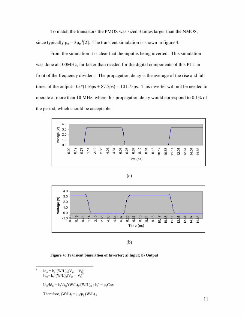
To match the transistors the PMOS was sized 3 times larger than the NMOS,
since typically µn = 3µp 1[2]. The transient simulation is shown in figure 4.
From the simulation it is clear that the input is being inverted. This simulation
was done at 100MHz, far faster than needed for the digital components of this PLL in
front of the frequency dividers. The propagation delay is the average of the rise and fall
times of the output: 0.5*(116ps + 87.5ps) = 101.75ps. This inverter will not be needed to
operate at more than 10 MHz, where this propagation delay would correspond to 0.1% of
the period, which should be acceptable.
0.01.02.03.04.0
0.00
0.19
0.73
1.14
2.10
2.65
4.08
4.64
6.07
6.26
6.67
8.10
8.61
9.13
10.1
7
10.6
8
11.1
1
12.0
8
12.6
4
14.0
7
14.6
3
Time (ns)
Volta
ge (V
)
(a)
-1.00.01.0
2.03.04.0
0.00
0.19
0.73
1.14
2.10
2.65
4.08
4.64
6.07
6.26
6.67
8.10
8.61
9.13
10.1
7
10.6
8
11.1
1
12.0
8
12.6
4
14.0
7
14.6
3
Time (ns)
Volta
ge (V
)
(b)
Figure 4: Transient Simulation of Inverter; a) Input; b) Output
1 Idp = kp’(W/L)p(Vgs – Vt)2
Idn= kn’(W/L)n(Vgs – Vt)2 Idp/Idn = kp’/kn’(W/L)p/(W/L)n ; kx’ = µxCox Therefore, (W/L)p = µn/µp (W/L) n

12
4.1.2 The NAND and NOR Gates These two circuits are needed for the construction of the PFD, as will be seen in
section 4.2.2. These gates are made in CMOS by using a PMOS pull-up network (PUN)
on top of a NMOS pull-down network (PDN); where the pull-up and pull-down outputs
are DeMorgan duals of each other [2]. These gates behave much like an inverter, with
the PUN charging capacitances and the PDN network discharging them. As such, much
of what has been said above holds true here and therefore, in this section, I will instead in
concentrate on how the logic of the gates is obtained.
For the NAND gate, shown in figure 5a, if either A or B is off then there will be a
current path from Vdd to the output, causing Vo to go to Vdd. Only when both A and B are
high will there be a current path to ground, allowing Vo to discharge to zero. This
provides the NAND logic Action.
The NOR gate, figure 5b, is simply the opposite of the NAND. The pull up
network is two PMOS in series, and the pull down is two NMOS in parallel. When A or
B is high, Vo discharges to zero, and only when both A and B are low does Vo charge to
Vdd.
(a) (b)
Figure 5: a) NAND gate; b) NOR gate

13
When sizing these circuits to match the currents of the pull-up and pull-down
networks, the worst case scenario must be taken into account to ensure the minimum
propagation delay [2]. This is done by modeling the transistors by their drain-source
resistances and switches. This is illustrated in figure 6.
Figure 6: Inverter Modeled by Drain-Source Resistances [2]
As is shown by equations 1 and 2 in figure 6, the drain source resistances are
inversely proportional to ratio of gate width to gate length (W/L). By using the same
method for finding equivalent resistances for series and parallel resistors, equations for
equivalent transistor sizing can be found, as shown in equations 3 and 4 below [2].
These equations were used to size the PUN and PDN to give a worst case
performance of at least that of the CMOS inverter. For the NAND the PMOS transistors
are in parallel thus according to equation 4, behave as a transistor twice as wide when
they are both on. Therefore, the worst case for the PMOS transistor is only one transistor

14
on. The NMOS transistors are in series, thus the only scenario where they create a
current path is when they are both on. Referring to equation 3, two transistors in series
behave as a transistor half as wide. Thus to maintain the worst case PMOS to NMOS
(W/L) ratio, the NMOS widths must be doubled from the standard width of 800nm. This
is reflected in figure 5a.
The NOR gate is the reverse of the NAND gate; that is, PMOS in series and
NMOS in parallel. Using the same method discussed above for the NAND, the PMOS
transistor widths were doubled from 2.4µm to 4.8µm and NMOS transistors were left at
the inverter size of the standard 800nm, as shown in figure 5b.
The output of the NAND and NOR gates is shown in figure 7. They were tested
by using two inputs, A and B, at frequencies of 40 MHz and 66.67 MHz driving a 10 fF
load.

15
Figure 7: Transient Simulation of NAND and NOR Gates
It can be seen that the both gates operate as they should. The NAND is low only
when both inputs A and B are high, and the NOR is high only when both A and B are
low. The propagation delays of the gates are: 86.8 ps for the NOR and 96.6 ps for the
NAND.
4.2 Phase/Frequency Detector
4.2.1 Background
The phase/frequency detector receives two signals and outputs the phase and/or
frequency difference that is between them. The average voltage on the outputs of the
PFD is proportional to the excess phase. The proportionality is modeled by the phase
constant Kphase [3, 5].
The PFD can be modeled as a three state machine, the state table of which is
shown in figure 8 [3]. The initial state is state 0, the inputs are shown by arrows and the
outputs are shown inside the state circles.
(a) (b)
Figure 8: a) PFD State Table [3]; b) Example output of state table
For example: Suppose there are two signals, A and B, with A leading by T/4
seconds, where T is the period of the signals. Starting in the initial state, state 0, A goes
high causing a transition to state 1. From the state table it is seen the outputs of state 1
are: Qa = 1 and Qb = 0. T/4 seconds later B goes high causing a transition back to state 0,

16
where the outputs are zero for both Qa and Qb. Thus, a high output of T/4 seconds has
been seen at output Qa. This shows that A leads B by T/4 seconds.
In PFD design one must be cautious of “deadzone”. Deadzone occurs when small
phase differences do not provide enough time between PFD input signals, A and B, for
the PFD to provide output signals with sufficient amplitude to switch the charge pump
[3, 4]. This prevents the loop from being able to correct small phase errors, resulting in
jitter in the output. Fortunately, however, by ensuring that the delay through the reset
AND gate is sufficiently large the output will always be able to achieve a full logic level;
thus, eliminating any deadzone.[3, 4] The delay in the AND gate can be seen when both
outputs Qa and Qb are simultaneously high. Also of note: This may give the appearance
of a fourth state, however it is merely the presence of the AND gate delay.
4.2.2 Circuit
The circuit that implements the state table in figure 8 is shown in figure 9a with
the flip-flop circuit shown in figure 9b [3]. The flip-flops produce a high output when the
rising edge of an input is received (at the clock input). This stays high until the other
flip-flop receives a rising edge, causing it to go high as well, causing a high-high input at
the AND gate, thereby resetting both flip-flops.

17
(a) (c)
Figure 9: a) PFD Block circuit [3]; c) D-Flip Flop Circuit [3]
The NOR gates in the flip flop are those mentioned earlier in section 4.1.2. The
reset AND gate is a combination of the NAND in section 4.1.2 and an inverter from
section 4.1.1.
4.2.3 Simulation and Results Transient simulations of the PFD are shown in figure 10. Figure 10a shows the
PFD operating with a phase difference; figure 10b a frequency difference. Both
simulations have the PFD driving the charge pump from section 4.3 as a load.
In figure 10a input A lags B by 70ns. This phase error is seen on output Qb in the
form of a 70% duty cycle. In figure 10b A is at 12.5 MHz and B is at 10 MHz. The
result is a constantly changing phase error--frequency is the derivative of phase. By
taking the slope of Qa from minimum to maximum phase error, the Kphase was found to be
1 V/rad.

18
In both figures Qa and Qb can be seen as being simultaneously high, thus ensuring
no deadzone.
In the loop the PFD is required to run at 4 MHz, therefore, these simulations at
minimum10 MHz suggest that the PFD should have no problem operating in the loop.
(a) (b)
Figure 10: Transient Simulation of PFD: a) Phase Error; b) Frequency Error

19
4.3 Charge Pump
4.3.1 Background The charge pump takes the output pulses of PFD and translates them into currents,
which are passed through the loop filter to produce a control voltage (Vcont) for the
voltage controlled oscillator (VCO). This control voltage raises or lowers the frequency
of the VCO. This can be illustrated in the conceptual circuit of figure 11. Switch 1 (S1)
is connected to Qa of the PFD and switch 2 (S2) to Qb. When Qa is high, S1 is closed
causing I1 to charge the loop filter. Likewise, when Qb is high, S2 is closed causing I2 to
discharge the loop filter. (note: the loop filter shown in the figure is for illustration only)
[3, 4, 5]
Since I1 and I2 set the control voltage it is intuitive that I1 and I2 must be matched,
so as to provide the same current. If they are not matched excess current in the direction
of the stronger current source will drive the control voltage to the supply rails. In a
closed loop, feedback will correct this mismatch; however, it will cause the loop to lock
with a finite phase error [3, 4]. Also of concern: When the loop is locked, S1 and S2 are
switched at the same instants. Inevitably, the switches will not have the exact same
capacitance and/or current, thus they will switch at different rates. This causes voltage
spikes in the output. These spikes modulate the VCO output with the reference, leading
to sidebands. This is referred to as “reference feed-through”. [3, 4]

20
Figure 11: Conceptual Charge Pump Circuit [3]
4.3.2 Circuit
The charge pump is implemented as the circuit in figure 12. The two current
sources, I1 and I2, have been implemented using current mirrors. I1 and S1 employ PMOS
transistors and I2 and S2 use NMOS transistors. The lengths of all transistors were set to
twice the minimum size at 700nm so as to increase the output resistance [6]. The widths
were then chosen large so as to minimize the amount of Vgs required. This was needed so
that it could operate close to the rail. [6]
To mitigate the charge pump design issues discussed in 4.3.1 great care was taken
to match I1, S1 with I2, S2. This involved using equations to get ballpark transistor
widths, then iterating in the simulator to match them as closely as possible. Figure 12,
shows the optimized charge pump circuit. Discussion of the testing methods is in the
next section, 4.3.3.
Since S1 is PMOS, its input must be inverted, hence the inverter at its input. In
order to match the capacitances seen at the gates of the switches, two inverters were
placed at the S2 gate.

21
Figure 12: Charge Pump Circuit
4.3.3 Simulation and Results
Testing/Optimizing of the charge pump was done by taking the preliminary
charge pump, of the same form of figure 12, and driving a 100 Ω resistor which was at
Vdd/2. As mentioned above, transistor widths were fine-tuned till the UP and DOWN
currents were as close as possible.
The currents for the cicuit of figure 12 were: UP current, Iup = 2.38 mA and
DOWN current, Idn = 2.35 mA. This represents a mismatch of 1.27%.

22
4.4 Frequency Divide-by-two Note: The full design of the frequency divide-by-two is not within of the scope of
this project. This is just a preliminary look at the design of divide-by-twos. The full
design of a divide-by-two could be explored by another student in the future.
4.4.1 Background The frequency divide-by-two halves the output frequency. This is to reduce the
complexity of the programmable divider [4]. It consists of two latches that are connected
as slave and master2 to form a flip flop. The output of the flip-flop is inverted and fed
back to the input. The block diagram of the divide-by-two is shown in figure 13.
Figure 13: Frequency Divide-by-two Block Diagram [4]
By connecting the flip-flop in this manner every clock edge the output inverts,
thereby providing a 50% duty cycle output at half the frequency of the clock input.
4.4.2 Circuit The latches are implemented as a differential pair and a regenerative pair [4]. The
circuit is shown in figure 14. Unlike the other circuits discussed so far, this circuit must
operate fast, at around 2 GHz. The transistors have been sized with large widths so as to
2 Output of master is connected to input of slave, with the slave’s clock signal being inverted from that of the master.

23
increase their transconductances to facilitate faster switching. The resistors also must be
small to limit parasitics, which slow the circuit. Additionally, the transistors must not
saturate, therefore Vds must be large, another reason for small resistors. The current
mirror is designed to sink around 4.5 mA. This level of current was needed to provide
enough voltage across the resistors and to switch the transistors quickly.
Figure 14: Latch circuit
4.4.3 Simulation and Results Testing began with a single latch at 2 GHz. The output of this simulation is seen
in figure 15. It can clearly be seen that it operates correctly; that is, it is transparent for
CK high, and latches the last value when CK goes low.
Connecting two latches in a slave master configuration (shown in figure 14) and
simulating resulted in figure 16. It is seen that after a brief start up transient the output
settles into a signal at half the rate of the input, with a 50% duty cycle.

24
Figure 15: Transient Simulation of Latch
Figure 16: Transient Simulation of Divide-by-Two
4.5 Phase-Locked Loop
4.5.1 Circuit Overview
To simulate the components to see how they function in a closed loop a PLL
testbench consisting of the PFD, charge pump, a simple passive filter, an ideal VCO and
the divider was built. The circuit is shown in figure 17. The inverters before the divider

25
serve to square up the VCO’s sinusoidal output; similarly the output inverters increase
the divider’s voltage swing to rail-to-rail.
Figure 17: PLL Test bench
4.5.2 Design
The VCO in the tuner that Kevin Cheung is designing has a center frequency of
1.85 GHz and a Kvco of 133 MHz. In lieu of a divider that could provide division factors
in the hundreds, the VCO parameters were scaled by a factor of 256 to yield a center
frequency of 7.22 MHz and a Kvco of 520 KHz for the ideal VCO. Scaling the values
facilitated testing the PLL with only the divide-by-two feedback while still providing an
accurate assessment of the loop dynamics, and implicitly, the operation of the PFD and
CP. Equations 5 and 6 give values for the natural frequency and damping constant,
respectively.
Because of the division in the feedback, the Kvco term in the above equations must
be divided by the division factor; in this case, two. Choosing a resistor value of 1.81 KΩ

26
and a capacitance of 1nF provided a slightly under-damped response of around 0.7071
and a natural frequency of 124 KHz.
4.5.3 Simulation and Results
Figure 18 shows the transient simulation of the loop. It can be seen that the loop
settles from the frequency error in 26us (ωnt = 3.33). Also, the crystal (XTAL) input
comes in at 4 MHz and the VCO feedback settles at 8 MHz3; showing the loop is
working as a frequency synthesizer--a division factor of 2 in the feedback causes a
doubling of the output frequency.
3 Vcont settles at 1.5V which according to the VCO output equation:
ω = (ωo = 7.22 MHz) + (Kvco = 520 KHz)*(Vcont = 1.5 V) = 8 MHz. This was corroborated by checking the period of the output sinusoid in the simulator.

27
Figure 18: Transient Simulation of PLL Test bench
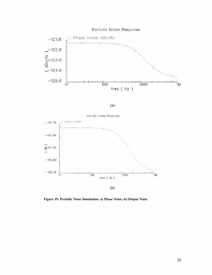
Periodic noise simulations are shown in figure 19. The simulations both illustrate
low pass responses with a corner frequencies of 88 KHz. Figure 19a shows phase noise.
The inband phase noise of -121.5 dBc/Hz is well within specification. Figure 19b shows
the output noise. The in-band output noise is -187.3 dB.
28
(a)
(b)
Figure 19: Periodic Noise Simulation: a) Phase Noise; b) Output Noise

29
5.0 Layout
Layout was done using a modular approach where the building blocks of the circuits were
laid out and tested separately. This was to prevent having to debug large complex
layouts. All layout was done in Cadence Virtuoso according to the design rules of
Canadian Microelectronic’s 0.35 micron CMOS technology. Each circuit was extracted
and compared via a “layout versus schematic (LVS)” comparison for uniformity between
layout and schematic. All post layout simulations were done using the same testbenches
and test parameters as the schematics to facilitate easy comparison between schematic
and layout circuits.
5.1 Inverter
The inverter layout is shown in figure 20. The PMOS is on top, the NMOS on the
bottom. The source and bulk contacts are connected to supply rails (vdd and gnd, PMOS,
NMOS respectively). The drains contacts are connected with metal1, and the output pin
is on this connection. The input pin is connected to the gate poly.
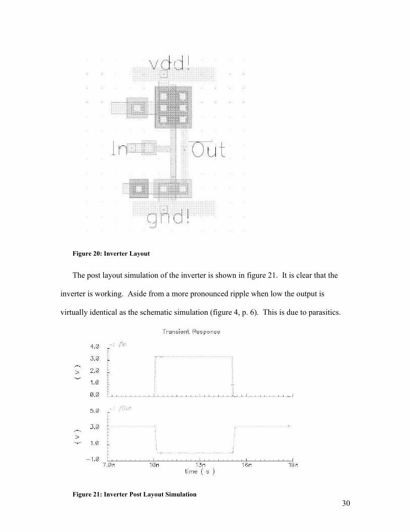
30
Figure 20: Inverter Layout
The post layout simulation of the inverter is shown in figure 21. It is clear that the
inverter is working. Aside from a more pronounced ripple when low the output is
virtually identical as the schematic simulation (figure 4, p. 6). This is due to parasitics.
Figure 21: Inverter Post Layout Simulation

31
5.2 NAND Gate The layout for the NAND gate can be seen in figure 21. Again the PMOS are on top,
NMOS on bottom. As can be seen in figure 5a (p.7) the drains of the PMOS are
connected as well as the source and drain for the NMOS. Instead of having two
completely discrete transistors connected with metal layers, the PUN and PDN transistors
were fused together. This conserved chip area and limited parasitics associated with
routing layers connecting nodes. Otherwise the layout for this gate was basically the
same as discussed for the inverter.
Figure 22: NAND Gate Layout
The post layout simulations for the NAND gate are shown in figure 23. Clearly
these simulations show the NAND gate operating properly, and with no noticeable side
effects of parasitics4.
4 This is not unreasonable. This simulation is done at 40-66 MHz. Parasitics aren’t significant at these relatively low frequencies. Additionally, this is a small circuit with little routing.

32
Figure 23: NAND Gate Post Layout Simulations
5.3 NOR Gate
The NOR gate layout is shown in figure 24. It was laid out following the same
procedure mentioned previously in the NAND layout (section 5.3).

33
Figure 24: NOR Gate Layout
Figure 25 shows the post layout simulation of the NOR gate. The simulations show
the circuit works properly.
Figure 25: NOR Gate Post Layout Simulation
34
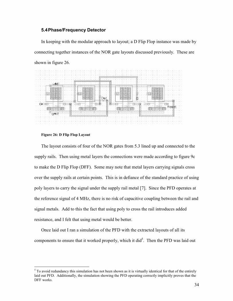
5.4 Phase/Frequency Detector
In keeping with the modular approach to layout; a D Flip Flop instance was made by
connecting together instances of the NOR gate layouts discussed previously. These are
shown in figure 26.
Figure 26: D Flip Flop Layout
The layout consists of four of the NOR gates from 5.3 lined up and connected to the
supply rails. Then using metal layers the connections were made according to figure 9c
to make the D Flip Flop (DFF). Some may note that metal layers carrying signals cross
over the supply rails at certain points. This is in defiance of the standard practice of using
poly layers to carry the signal under the supply rail metal [7]. Since the PFD operates at
the reference signal of 4 MHz, there is no risk of capacitive coupling between the rail and
signal metals. Add to this the fact that using poly to cross the rail introduces added
resistance, and I felt that using metal would be better.
Once laid out I ran a simulation of the PFD with the extracted layouts of all its
components to ensure that it worked properly, which it did5. Then the PFD was laid out
5 To avoid redundancy this simulation has not been shown as it is virtually identical for that of the entirely laid out PFD. Additionally, the simulation showing the PFD operating correctly implicitly proves that the DFF works.

35
using instances of the aforementioned building blocks according to the schematic in
figure 9a. The layout is shown in figure 27.
Figure 27: PFD Layout
The simulation of the PFD is shown in figure 28. It shows the PFD working for a
frequency difference. The circuit is performing correctly and shows negligible effect
from parasitics.
Figure 28: Post Layout Simulation for PFD

36
5.4 Charge Pump
The charge pump layout is shown in figure 29. The layout of this circuit was more
involved than the previous circuits because of the very wide transistors. To keep
resistance associated with the gate poly low transistors had to be “fingered”[7].
Fingering is when several transistors are placed in parallel, with their sources and drains
connected. The gate poly is then connected via a metal layer. This allows relatively
short lengths of gate poly (3µm vs. 120µm).
The charge pump circuit (figure 12) also needs two 1 kΩ bias resistors. These were
implemented by laying poly over top of an n-well. Poly resistance is proportional to
(L/W) [7]; thus one can get the desired resistance by simply playing with the geometry of
the poly. The serpentine pattern makes the resistor more compact. After several
iterations, the resistors gave an extracted resistance of 1000.52 Ω. Inverters were
implemented with those of 5.1.

37
Figure 29: Charge-Pump Layout
Simulating the laid out charge pump in the same fashion described in 4.3.3, the UP
current, Iup = 2.283 mA, and the DOWN current, Idn = 2.397 mA. This represents a

38
mismatch of 4.9%, up from 1.27% in 4.3.3. This could probably be improved with a
better layout (see 7.0 Future Work and Recommendations).
5.5 PLL
Once the PFD and charge pump were laid out and tested individually; they were again
placed into the PLL testbench of 4.5.1 (figure 17) and simulated. The simulation is
shown in figure 30.
Figure 30: PLL Post-Layout Simulation
It is clearly seen that the curve matches that of the schematic circuit, with the loop
showing a slightly under-damped response settling at 1.5 V (corresponding to the loop
locking at 8 MHz) within 26µs, same as before.
Noise simulations were also run on the PLL. Periodic noise simulations are shown in
figure 31. Again, the simulations follow the low pass characteristic, with a corner
frequency at around 88 KHz. Phase noise is shown in figure 31a. In-band phase noise

39
has increased to -113.46 dBc/Hz, however, this is still within specification. Output noise
is seen in figure 31b. Output noise has increase to -174.6 dB.
(a)
(b)
Figure 31: PLL Post-Layout Periodic Noise Simulations: a) Phase Noise; b) Output Noise

40
6.0 Conclusions This project was to build a cable tuner for the DOCSIS market. It was a group project
with six members. Each member was responsible for a specific block. My work was
localized within the second frequency synthesizer; specifically, the phase-frequency
detector, charge pump and divide-by-two.
The phase-frequency detector and charge pump in addition to being designed, had to be
laid out. The divide-by-two on the other hand was simply to be designed as an
exploratory exercise—the formal design of which is left to a future student.
The phase-frequency detector was made up of smaller digital logic gates. Each of those
smaller sub-circuits had to first be built and tested, then assembled together. The
resulting phase-frequency detector functioned properly even at frequencies much greater
than needed, while also showing immunity to deadzone effects. Post layout, the circuit
still continued to function properly, with negligible effect of parasitics.
The charge pump was built and optimized for current matching for its charge UP and
charge DOWN currents. The optimized design in the schematic provided an UP current
of 2.38 mA and a DOWN current of 2.35 mA, representing less than 1.27% current
mismatch. After layout, the UP current decreased to 2.283 mA and the DOWN current
increased to 2.397 mA, representing a 4.9% current mismatch. If time permitted a more
careful layout might have improved this.
The divide-by-two was built from two latches arranged to form a flip-flop. Design began
with a single latch, tested until it could operate at 2 GHz. Then two latches were
arranged as a flip-flop and tested at 2 GHz. It was seen that the input 2 GHz signal was

41
outputted at 1 GHz, with a 50% duty-cycle showing that the divide-by-two functioned
properly.
Once each component was built and tested individually, they were assembled into a
phase-locked loop testbench and simulated. This test-bench consisted of: the designed
phase frequency detector; charge pump and divide-by-two, as well as: a simple passive
RC low-pass filter, and an ideal voltage controlled oscillator. This loop was simulated
with first the design schematics, then with the extracted layout designs. The loop
functioned properly in each case; taking a 4 MHz reference signal input and settling to an
8 MHz sinusoid VCO output within 26µs.
Periodic noise analysis was performed on the cascaded phase-frequency detector and
charge pump. In-band phase noise was found to be -121 dBc/Hz for the schematic,
-113 dBc/Hz for the extracted layout; output noise was -187.3 dB for the schematic, and
-174.4 dB for the extracted layout.
In the course of the past eight months it can be seen that the components of the frequency
synthesizer for which I was responsible were successfully built. In addition to the
technical knowledge, I gained invaluable experience working with Cadence, an industry
standard software package. I also got to experience working within an engineering work
group. In the end I believe this was a successful project that will provide good
experience for my career.

42
7.0 Future Work and Recommendations Going forward from this point, I would like to do a more in depth look at noise analysis
of synthesizers/PLLs. It would also be nice to have a programmable divider to work with
to test the synthesizer at 1.85 GHz. I believe the charge pump layout could be improved
to lower the mismatch between current sources by adjusting the bias resistors and/or
transistor sizings.
I recommend this project to future students; it provided a good learning opportunity and
was enjoyable.
43
8.0 References [1] John W. M. Rogers, Brian Robar, Walt Bax, Zhan F. Zhou, Sivakumar Kanesapillai,
Stefan Fulga, Mike Toner and David Rahn., A Completely Integrated Cable Tuner, SiGe
Semiconductor
[2] Sedra and Smith, Microelectronic Circuits, Oxford, 1998, 4th Edition, p.1045-1068
[3] Behzad Razavi, Monolithic Phase-Locked Loops and Recover Circuits: Theory and
Design, IEEE Press, 1996, p.1-31.
[4] Behzad Razavi, RF Microelectronics, Prentice Hall, 1998, p. 247-293
[5] Calvin Plett, 97.455 Telecommunications Circuits: Course Notes, Carleton IEEE,
2001, p. 41-65
[6] Len MacEachern, 97.477 Analog Integrated Electronics: Course Notes, 2001,
p. 40-49.
[7] Garry Tarr, 97.469 Integrated Circuit Design and Fabrication: Course Notes, 2002.