Embed Size (px)
Citation preview

© 2012 IEEE
Proceedings of the IEEE Energy Conversion Congress and Exposition (ECCE USA 2012), Raleigh, USA, September 16-20, 2012
Accurate Equivalent Circuit Modeling of a Medium-Voltage and High-Frequency Coaxial WindingDC-Link Transformer for Solid State Transformer Applications
S. Baek,B. Cougo,S. Bhattacharya,G. Ortiz
This material is published in order to provide access to research results of the Power Electronic Systems Laboratory / D-ITET / ETH Zurich. Internal or personal use of this material is permitted. However, permission to reprint/republish this material for advertising or promotional purposes or for creating new collective works for resale or redistribution must be obtained from the copyright holder. By choosing to view this document, you agree to all provisions of the copyright laws protecting it.

Accurate Equivalent Circuit Modeling of a Medium- Voltage and High-Frequency Coaxial Winding DC-link Transformer for Solid State Transformer Applications
Seunghun Samuel Baek ECE dept. North Carolina State University
Raleigh, United States of America [email protected]
Subhashish Bhattacharya
ECE dept. North Carolina State University Raleigh, United States of America
Bernardo Cougo Laplace, University of Toulouse
Toulouse, France [email protected]
Gabriel Ortiz
Power Electronic Systems Laboratory, ETH Zurich Zurich, Switzerland
Abstract— The 12kV-400V dc-dc stage of a distribution level solid state transformers (SST) has been under research and development. Development of a 15kV SiC Mosfet allows a single stage of the dc-dc converter to operate at medium voltage at an operating frequency of over 20kHz. Nonetheless, the high rising and falling time during pulse switching in the dual active bridge operation is another significant obstacle to realize this technology. In order to understand and predict the frequency response with pulse switching and consider common-mode response via circuit analysis accurately, lumped-element equivalent circuit model has been developed for broadband coaxial winding transformer (CWT) with analytic expressions. The simple lumped-element equivalent circuit introduced in this paper has been verified by measurement results from a prototype for a medium-voltage (MV) and high frequency (HF) coaxial winding power transformer up to the frequency where the length of the coaxial body is a quarter of a wavelength and further study up to 30MHz has been described.
I. NOMENCLATURE ε Permittivity of free space µ Permeability of free space c Speed of light in a free space σ Conductivity λ Wavelength β Phase constant f Frequency / Quarter-wavelength n Turns ratio N The number of turns i √ 1 Z Characteristic impedance Z Input impedance l Total length of the coaxial geometry w Width of the the coaxial geometry WE Stored electrical energy
Figure 1. 12kV-400V dc-dc stage of a solid state transformer application CCM Common-mode capacitance C Effective capacitance between node ‘A’and ’B’ C , Static capacitance per unit area in the ‘i’ th layer P Permeance
Distributed lumped inductance per unit length Distributed lumped capacitance per unit length D Diameter of bare copper wire d A half of the effective thickness of a layer of winding on
the basis of copper area LV Low-voltage winding HV High-voltage winding oc Open circuit sc Short circuit HV B-D sc
Short circuit measuments from the HV side with connection ‘B’and’D’ nodes
II. INTRODUCTION The core element of the future smart distribution system
is the power electronic-based distribution transformer using power semiconductor devices, so called solid state transformer (SST). It will replace the 50Hz and 60Hz bulky line transformers with advantages of being compact and having additional functionalities, such as control of active/reactive power flow and protection against voltage sag
HVVmidV LVV
978-1-4673-0803-8/12/$31.00 ©2012 IEEE 1439
and over current. In order to realize high frequency operation at high voltage, the effect of parasitic elements has to be predicted and controlled in advance. The Dual Active Bridge (DAB) dc-dc converter is one of the mostly used topology to reduce the switching stress and losses on power devices at high frequency. However, the high dv/dt during pulse switching possibly causes high current overshoot and serious damage on power devices. Therefore, it is important to mitigate and predict the influence of parasitic elements, especially capacitances.
The conventional method to design high voltage transformer design is to use large number of turns and multiple sections to reduce electric stress between wires and layers [2]. However, this method leads to high parasitic capacitances and complexity of the geometry which makes the performance of the transformer less predictable. A coaxial-winding transformer (CWT) with low number of turns guarantees low parasitic elements and the simple symmetric geometry allows it to be more predictable.
A Simple lumped-element equivalent circuit models for CWT up to 30MHz is introduced in section ΙΙΙ and analytical modeling and calculation are described and verified with finite element methods (FEM) and measurements in Section ΙV. The test results during operation and fabrication process are briefly shown in Section V.
III. LUMPED- ELEMENT EQUIVALENT CIRCUIT MODEL OF CWT
A. Existing equivalent circuit model An energy based approach with six capacitances has been
used to represent three input two winding transformers in Fig. 2 (a) [3]-[7]. As long as the propagation delay can be ignored, this model has given a reliable representation of open and short circuit impedance with three inputs up to the working frequency from the power conversion point of view. The values of the capacitances and inductances are determined by resonant peaks in the impedance plot in different connections and this method has been proven useful for the conventional power transformer applications. However, some values are not in measurable range, especially in case of MV-HF DC-link CWT for SST applications, and the negative values from mathematical calculation [7] make it difficult to perceive the impact of the parasitic elements on the circuit intuitively without calculation.
The frequency response of the prototype with low parasitic elements and large turns ratio shows different, but clearer, pattern due to simple symmetric geometry. A new simple equivalent circuit model for a coaxial winding transformer is introduced in this paper.
The simple equivalent model valid, approximately, up to the frequency / where the first resonance occurs by leakage inductance and effective capacitance has been developed and different analysis by transmission line theory is used for frequencies over / . The results of the
proposed equivalent circuit model is representing the electromagnetic behavior of the two winding CWT with large turns ratio within / and the capacitance values literally corresponds to the amount of electrostatic energy on the nodes.
B. Characteristics of frequency response on windings of CWT and measurements at 30MHz Let us say that ‘ ’ on node ‘A’ and ‘B’ and ‘ ’ on node
‘C’ and ‘D’ represents electric potential on low voltage winding and high voltage winding of coaxial winding transformer, respectively. The electric energy stored within transformer by on low voltage side is relatively small in geometry l > w in Table I and the contribution on the effective capacitance is significantly mitigated by the factor of ‘ 1/ ’ referred to high voltage side. Therefore, on the low voltage winding, which has a single turn of copper tubes in the z direction, can be ignores as if shorted, = 0, in Fig. 3 from electrostatic point of view. This assumption allows simple and clear analysis without causing significant error in calculation in two dimensions on r - plane. Also, it is based on the conventional method of calculating parasitic capacitances of windings, which considers one turn as equipotential body for calculation in two dimensions.
Under this assumption, the low voltage winding can be seen shorted, then the electric energy stored with six capacitors notation in Fig. 2 can be represented by , = ( ) ( )( )
= ( ) . (1)
and simplified with three capacitances calculated as
= , = , = . (2)
Considering the contribution of the electric energy stored from the low voltage winding is negligible referred to the high voltage winding side, the electrostatic characteristics of the transformer can be represented with three capacitances in Fig. 2(b). For the measurement, frequencies of the series and parallel resonant peaks have been used [3], [4] and simple capacitance measurements in six different connections [6] can be also used. In either fashion, there are only three capacitance values are achievable on the basis of the impedance plot or capacitance measurements in six different connections alike.
Because electric and magnetic field distribution within the transformer with connection from high voltage side to ‘C’ or ‘D’ nodes are symmetric, the frequency responses by this
TABLE I. ELECTROSTATIC ENERGY STORED BY INDEPENDENT INPUT VOLTAGES Excitation ( = , , ( · ) . )= 1 , = = 0 28 · 10 J= 1 , = = 0 69 · 10 J= 1 , = = 0 16 · 10 J
1440

Figure 2. Conventional six capacitances representaton for three voltage
inputs (a) and simplified three capacitance representation (b)
rθZ
2V
3V
2V
1V
2/l
w Figure 3. Views on r-z plane (left) and r- plane (right)
scL
aCocL2
2/cC
2/cC
2/bC
2/bC Figure 4. Equivalent circuit model of CWT (~ 1/4 λ)
connections should be the same. It can be seen that one turn in z direction is equipotential under the aforementioned assumption. Therefore, the input impedance measurements from connection B-C and B-D, and the measurements from connection A-C and A-D are always identical.
The first parallel resonance frequencies caused by and from open circuit measurements are the same from either side, and the first parallel resonance frequency of short circuit measurements from high voltage side and the series resonance frequency of short circuit measurements from low voltage side caused by and are almost the same as well in Fig. 5.
1) Low voltage winding side The electrical energy stored within the transformer
depends not on the voltage on low voltage winding but on the voltage on the high voltage winding dominantly on the r-
plane with large ‘n’. This means the effective capacitance
interacts with and on low voltage side is the capacitance seen from the high voltage side by magnetic coupling. Hence, there are series and parallel resonance between , and transformed from high voltage side in case of open circuit measurements, however, only inductance is measured on low voltage side with shorting high voltage winding terminals within 30MHz in Fig. 5.
2) High voltage winding side The magnetizing inductance resonates with the
capacitance in parallel at the same frequency when measured from the low voltage side. After the magnetizing inductance is nulled by the capacitance in parallel, the response shows multi resonance up to 30MHz with distributed inductances
and capacitances by transmission line theory in Fig. 6 regardless of short or open connection of low voltage side terminal as can be seen as shorted by assumption.
C. Integration of electrostatic and magnetostatic model and equivalent circuit representation. It is tricky to represent electromagnetic behavior in three
dimension with circuit theory in one dimension over a wide range of frequency, however, a simple equivalent circuit model can be developed in frequency range of interest, approximately up to the frequency where the length of the coaxial geometry is a quarter of wavelength from power conversion point of view.
1) Frequency response up to / If conventional six capacitances notation in Fig. 2 is used,
the capacitance values calculated through circuit theory with connection B-C and B-D, A-C and A-D are almost the same with a large ‘n’ approximation [7]. Hence, only three values, ‘ ’, ‘ ’ and ‘ ’, matter with a large ‘n’, which are also the three valid measurement results. Therefore an electromagnetically integrated circuit can be represented by three capacitance and two inductance values as in Fig. 4.
This equivalent circuit has one parallel resonance frequency from high voltage side which is determined by and with by the termination of the low voltage. On
TABLE II. EFFECTIV CAPACITANCES (~1/4 WAVELENGTH)
Connection between node ‘A’ and ‘B’ Large ‘n’ approximation
A-B and C-D
= ( ) B-D ( 1) 1 ( )
= ( ) B-C ( 1) 1 ( )
A-D ( 1) 1 ( ) =
( ) A-C ( 1) 1 ( )
1C2C
3C
4C
6C 5C1V 2V
3V
aC cC
bC
1V
3V
1441

Figure 5. Impedance modulus (top) and argument [º] (bottom) with frequency [Hz] of the CWT prototype
TABLE III. DIMENSIONS OF THE CWT PROTOTYPE
3.2 8.5 15.5 0.39 0.33 0.34 25.4 27.0 59.5 81 4.3 2.24
low voltage side, both series and parallel resonances occur by combination of , and at open circuit measurements and only inductive element remains at short circuit measurements in measurable frequency range.
The frequency response over the frequency when series resonance by and occurs are almost the same regardless of the termination of the opposite side winding.
This equivalent circuit can represent the resonant peaks in different connections for CWT applications with large ‘n’. The capacitance values are always positive and directly represent physical quantities of the electrical energy stored with respect to the connected nodes in contrast to the six capacitances model. Note that the approximation is based on the assumption l > w and large turns ratio ‘n’, that is, the equivalent circuit model becomes more accurate with long cylindrical shape and large turns ratio. Considering a quarter of the wavelength of the CWT prototype for SST applications is around 4MHz, which is around several hundred times of the operating switching frequency, 20 kHz. Therefore, the equivalent circuit in Fig. 4 is sufficient to
represent the frequency response of a high step up-down coaxial winding power transformer in practice.
The three capacitance values are easily achieved with three simple measurements when = 0 , = 0 and = by shorting two nodes at a time.
1) Frequency response in the range / -30MHz
Further study can be done for better understanding higher frequency response up to 30MHz. From frequency at which the length of the coaxial geometry is longer than a quarter of
),(1 tzI
),(2 tzI
zL d Δ
zCdΔ
),(1 tzzI Δ+
),(2 tzzI Δ+
),(1 tzzV Δ+),(1 tzV
),(2 tzV Figure 6. A circuit representation from HV side by transmission line
theory in the range of 1/4 λ ~ 30MHz
1.00E-021.00E+001.00E+021.00E+041.00E+06
1.00E+03 1.00E+04 1.00E+05 1.00E+06 1.00E+071.00E-041.00E-02
1.00E+001.00E+021.00E+04
1.00E+03 1.00E+04 1.00E+05 1.00E+06 1.00E+07
-90-70-50-30-101030507090
1.00E+03 1.00E+04 1.00E+05 1.00E+06 1.00E+07
-90-70-50-30-101030507090
1.00E+03 1.00E+04 1.00E+05 1.00E+06 1.00E+07
HV A-D sc HV B-D sc
LV B-D oc LV A-D oc
HV A-D oc HV B-D oc
LV A-D sc LV B-D sc
/ ,
/ ,
Modulus Modulus
Argument Argument
1442

Figure 7. Modulus (top) and argument (bottom) of in case of
‘HV B-D sc’ in the range of 3MHz~30MHz
wavelength, lumped-element model of a transmission line can be applied with distributed series inductance and shunt capacitance per unit length for the lossless case in Fig. 6. The effect of the magnetic coupling can be neglected in the given frequency range and represented with respect to the infinitesimal length dz over the transmission line. In case of ‘B’ and ‘D’ connection, the change in voltage and current per unit length are given in (4) under the condition (3) ( ) = ( ) ( ) , ( ) 0, (3) ( , ) = = · ( , ) ( , ) = · ( , ). (4)
The voltage and current at ‘z’ in phasor notation are
( ) = · · , ( ) = · · (5) where the phase constant, β = , and characteristic
impedance, = .
Then, the input impedance is given by = = ( )( ) = · . (6) The frequency where a length of the coaxial geometry is
a quarter of wavelength in case of A-D and B-D connections are 3.2MHz and 4.2MHz respectively by calculating with inductance and capacitance per unit length form 2D FEM results in Table IV and Table V without considering the effect on the edges.
The responses from the high voltage side are almost the same regardless of the open or short connection on low
voltage terminals. The response from the low voltage winding side with connection of A-B-D and A-B-C nodes is seen as purely inductive up to 30MHz due to almost no electric energy stored with shorting high voltage side terminals.
IV. ANALYTICAL EXPRESSIONS AND CALCULATIONS OF PARASITIC ELEMENTS OF CWT
The calculation method has been well explained in literatures [6]-[14] so the equations are introduced concisely in this section.
A. Inductance model and calculation for CWT The flux density and relative permeability of a magnetic
core is not directly measurable in most practical cases, hence, the effective of the Vtroperm500F nonocrystalline tape wound cores (T6004 − L2080 −W628) is calculated, 2.87 · 10 , on the basis of the measured inductance and effective cross sectional area given by the datasheet. The configuration and notations are in Fig. 9.
The inductances referred to the HV side are given by = · , ( = ) (7) = · ∑ . (8)
Calculation and FEM results in two dimensions have a good agreement in Table IV. Even though the errors between 2D calculation and measurements are high, minimization of the parasitic inductance is a concern rather than accuracy in this application and a certain amount of parasitic inductance from edges and connections are not avoidable so that error ratio becomes high compared to the low inductance in the coaxial body.
B. Capacitance model and calculation for CWT The parasitic capacitance calculation is conducted on
Cartesian coordinate in two dimensions for simplicity. More accurate calculation is also possible on cylindrical coordinates; however, the error generated by the difference on Cartesian and cylindrical coordinates is not significant over errors from geometrical imperfection. The effective capacitances for circuit analysis are calculated by stored electrical energy and voltage distribution between layers. = ∑ , ( ) ( ) = , ( , = ) (9)
TABLE IV. INDUCTANCES
Calculation in 2D 118nH/m 1.38mH/m
2D FEM 62nH(128nH/m) 658uH(1.37mH/m)
3D FEM 271nH 658uH
Measurements 715nH 519uH
1.00E+00
1.00E+02
1.00E+04
3.00E+05 3.00E+06 3.00E+07[Hz]
Measurement
Calculation
-100
-80
-60
-40
-20
0
20
40
60
80
100
3.00E+05 3.00E+06 3.00E+07
[ °] [Hz]
1443
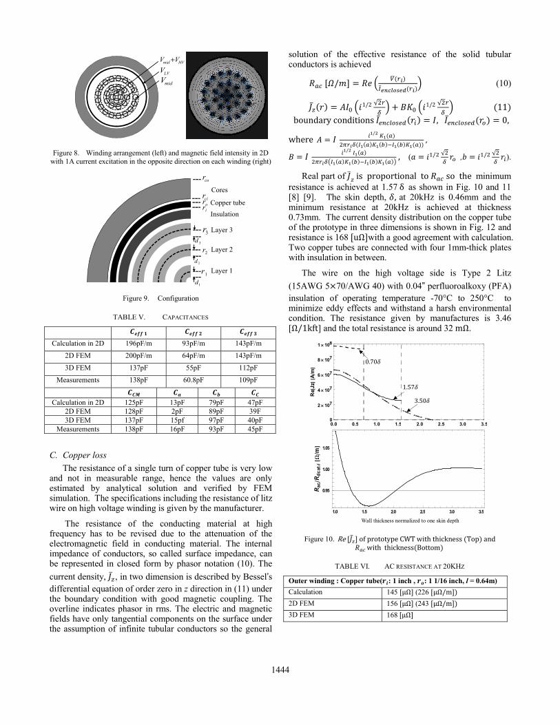
Figure 8. Winding arrangement (left) and magnetic field intensity in 2D
with 1A current excitation in the opposite direction on each winding (right)
Figure 9. Configuration
TABLE V. CAPACITANCES
Calculation in 2D 196pF/m 93pF/m 143pF/m
2D FEM 200pF/m 64pF/m 143pF/m
3D FEM 137pF 55pF 112pF
Measurements 138pF 60.8pF 109pF
Calculation in 2D 125pF 13pF 79pF 47pF
2D FEM 128pF 2pF 89pF 39F 3D FEM 137pF 15pf 97pF 40pF
Measurements 138pF 16pF 93pF 45pF
C. Copper loss The resistance of a single turn of copper tube is very low
and not in measurable range, hence the values are only estimated by analytical solution and verified by FEM simulation. The specifications including the resistance of litz wire on high voltage winding is given by the manufacturer.
The resistance of the conducting material at high frequency has to be revised due to the attenuation of the electromagnetic field in conducting material. The internal impedance of conductors, so called surface impedance, can be represented in closed form by phasor notation (10). The current density, , in two dimension is described by Bessel’s differential equation of order zero in z direction in (11) under the boundary condition with good magnetic coupling. The overline indicates phasor in rms. The electric and magnetic fields have only tangential components on the surface under the assumption of infinite tubular conductors so the general
solution of the effective resistance of the solid tubular conductors is achieved [ / ] = ( ) ( ) (10) ( ) = 1/2 √ 1/2 √ (11) boundary conditions ( ) = , ( ) = 0, where = / ( )( ( ) ( ) ( ) ( )) , = / ( )( ) ( ) ( ) ( ) , ( = / √ , = / √ ).
Real part of is proportional to so the minimum resistance is achieved at 1.57 δ as shown in Fig. 10 and 11 [8] [9]. The skin depth, , at 20kHz is 0.46mm and the minimum resistance at 20kHz is achieved at thickness 0.73mm. The current density distribution on the copper tube of the prototype in three dimensions is shown in Fig. 12 and resistance is 168 [uΩ]with a good agreement with calculation. Two copper tubes are connected with four 1mm-thick plates with insulation in between.
The wire on the high voltage side is Type 2 Litz (15AWG 5 70/AWG 40) with 0.04” perfluoroalkoxy (PFA) insulation of operating temperature -70°C to 250°C to minimize eddy effects and withstand a harsh environmental condition. The resistance given by manufactures is 3.46 [Ω/1kft] and the total resistance is around 32 mΩ.
Figure 10. Re [ ] of prototype CWT with thickness (Top) and with thickness(Bottom)
TABLE VI. AC RESISTANCE AT 20KHZ
Outer winding : Copper tube( : 1 inch , : 1 1/16 inch, l = 0.64m) Calculation 145 [µΩ] (226 [µΩ/m]) 2D FEM 156 [µΩ] (243 [µΩ/m]) 3D FEM 168 [µΩ]
0.0 0.5 1.0 1.5 2.0 2.5 3.0 3.50
2¥ 107
4¥ 107
6¥ 107
8¥ 107
1¥ 108
Re@JzD@A
êmD
1.0 1.5 2.0 2.5 3.0 3.5
0.95
1.00
1.05
Wall thicknessnormalizedto one skindepth
R acêR dcat
d@WêmD
1r
2r
3r
orcir
corCores
InsulationCopper tube
Layer 3
Layer 2
Layer 1
1d
2d
3d
ir
midVLVV
HVmid VV +
0.701.57 3.50
Wall thickness normalized to one skin depth
1444

Figure 11. Electric field intensity for the swiching states when positive node(left) and negative node(right) of DC link voltage is connected.
TABLE VII. AC DIELECTRIC BREAKDOWN TEST AND TEMPERATURE RISE . Cooling method Ambient temp. . 20kHz 200Vrms and 6kVrms square wave on LV and
HV side repectively under no load condition 60 min. Natural convection 23ºC 84ºC
Figure 12. Current density distribution
D. Core loss Core loss of Vitroperm 500F(T60004-L2080-W628) with
response to square wave excitation at operating frequency 20kHz is measured with Yokogawa WT3000 and the coefficients are extracted for the specific case under square wave excitation with duty ratio 0.5 = · ( =5.65, =2.12) (12)
V. TEST RESULTS AND FABLICATION OF CWT PROTOTYPE FOR SST APPLICATIONS
Good coaxial winding power transformer design for high bandwidth operation is a compromise among the given requirements, parasitic capacitance, inductance and distance to provide enough insulation on the top of efficiency. The distance between two windings is trade-offs between parasitic capacitance and inductance. For this specific application for the SST, the leakage inductance can be utilized for dual active bridge operation so leakage was not taken into consideration and the size of the transformer is chosen from the parasitic capacitance and insulation point of view.
A. Insulation strategy and FEM results
The prototype built for SST application has been designed as a dry-type transformer with an environmental concern. Hence, the insulation method has been carefully
strategized with room for safety at university level and estimated by FEM simulation in advance.
The proposed winding method for coaxial type transformer is shown in Fig. 8. Each turn of the high voltage winding is arranged in order to have lower electric potential between layers. Each layer of turns electrically shield to each other and the turn which has the highest electric potential is located the innermost layer to be electrically screened by other layers. The electrostatic field distributions in two dimensions are investigated by FEM for two switching states and the highest electric field is approximately 2.64MV/m between the first and last turn in the first layer when 12kVDC link voltage and 6kVDC at the neutral point are excited on the high voltage winding terminal in Fig. 11.
A DC dielectric breakdown Test was conducted on the prototype at 9.5kVDC between both windings for 60 seconds, and there was no air breakdown or dielectric failure while remaining leakage current 0.7mA. An AC insulation test was done by exciting 200V square wave from low voltage side under no load condition as shown in Table VIII. There was no sign of electrical failure or heat problems without cooling method for 60 minutes.
B. Power loss and temperature rise The prototype and the view with case are shown in Fig.
13. An open circuit test has been done without active cooling method at ambient temperature 23ºC in Fig. 14. Core loss and hot spot temperature were stabilized at 150W and 84 ºC respectively after 60 minutes operation and heat is uniformly distributed on the wide and round surface without air-gap in Fig. 14. There is no additional losses or heat issues without active cooling method as planned. Even though full load test has not been completed yet, the copper loss is expected to be less than 5% of the total loss for a power transfer of 30kVA, so it is reasonable to estimate the final results on the basis of open circuit test.
1445

Figure 13. Dry-type MV-HF CWT
VI. CONCLUSION The simple equivalent circuit model and analytical
calculation to represent the high frequency behavior of a coaxial winding power transformer was introduced in this paper. The solution and procedures were verified by finite element simulation and measurement results. The MV-HF coaxial winding power transformer has low parasitic parameters and ideal geometry for uniformly and symmetrically distributed electromagnetic flux with good electric and magnetic shielding.
The test results have shown the feasibility and the advantages of CWT as a link transformer at medium voltage power conversion in distribution line. The overall efficiency is expected to be up to 99.5% remaining below 100 °C under oil-free and natural convection condition for a power transfer of 30kVA. Even though the prototype is oversized for safety at high voltage stress, it is fairly compact with many advantages.
For the last few decades, conventional line transformers have been sufficient to meet the requirement of low frequency line transformers. As an increase of switching frequency of power electronic-based line transformers becomes necessary for reduction of the system size, coaxial winding power transformers will be able to play an important role as a high frequency DC link transformer.
Figure 14. No-load test set-up (left) and temerature measuremnt after 60
minutes operation without active cooling method (right)
REFERENCES [1] Seunghun Baek, Subhashish Bhattacharya, “Analytical modeling of a
MV-HF resonant coaxial type power transformer for a solid state transformer application”, ECCE2011, 2011.
[2] Luca Dalessandro Fabiana da Silveira Cavalcante, and Johann W. Kolar, Self-Capacitance of High-Voltage Transformers, IEEE Transactions on power electronics, VOL. 22, NO. 5, September 2007
[3] Bruno Cogitore, Jean-pierre Keradec, Jean Barbaroux, “The Two Winding Transformer: An Experimental Method to Obtain a wide Frequency Range Equivalent Circuit”, IEEE Transactions on instrumentation and measurement,Vol 40, No. 2, April 1994.
[4] Francois BLACHE, Jean-pierre Keradec, Bruno Cogitore, “Stray Capacitances of Two Winding Transformers:Equivalent Circuit, Measurements, Calculation and Lowering”, IEEE, 1994.
[5] Juergen Biela and Johann W. Kolar, “Using Transformer Parasitics for Resonant Converters-A Review of the Calculation of the Stray Capacitance of Transformers”, IEEE Transactions on industry applications,Vol 44, No. 1, January/February 2008.
[6] J. Biela, D. Bortis, J. W. Kolar, “Design Procedure for Compact Pulse Transformers with Rectangular Pulse Shape and Fast Rise Times”, IEEE transactions on Dielectrics and Electrical Insulation Vol.18, No.4;August 2011.
[7] Eric Laveuve, Jean-pierre Keradec, Michel Bensoam, Electrostatic of Wound Components: Analytical Results, Simulation and Experimental Validation of the Parasitic Capacitance, IEEE, 1991.
[8] Mark S. Rauls, Donald W. Novotny, Deepakraj M. Divan, Design Considerations for High-Frequency Coaxial Winding Power Transformers, IEEE Transactions on industry applications, Vol 29, No. 2, 1993.
[9] Mark S. Rauls, Donald W. Novotny, Deepakraj M. Divan, Multiturn High-Frequency Coaxial Winding Power Transformers, IEEE Transactions on industry applications, Vol 31, No.1, 1995.
[10] Mustansir H, Kheraluwala, Donald W. Novotny, Deepakraj M. Divan, Eric D. Baumann, Coaxially Wound Transformers for High-Frequency Application, IEEE Transactions on industry applications, Vol 28, No. 6, 1992.
[11] Antonio Massarini and Marian K. Kazimierczuk, Self-Capacitance of Inductors, IEEE Transactions on power electronics,Vol 12, No. 4, July 1997.
[12] Vedran Boras, Slavko Vujevic, Dino Lovric, Definition and Computation of Cylindrical Conductor Internal Impedance for Large Parameters, ICECom, 2010 Conference Proceedings, Sept. 2010.
[13] Hurbert Bristol Dwight, Skin Effect and Proximity Effect in Tubular Conductors, Transactions A.I.E.E., New York, N.Y., February 15-17,1922. 6
1446