Embed Size (px)
Citation preview

Accelerating WBG Power Electronics Commercialization FREEDM Annual Meeting
April 11, 2019Dr. Victor Veliadis Deputy Executive Director and CTO, PowerAmericaProfessor ECE North Carolina State University, Raleigh, NC [email protected]

GaN/SiC Power Devices Allow for More Efficient and Novel Power Electronics
Large Bandgap and Critical Electric Field allow for high voltage devices with thinner layers: lower resistance and associated conduction lossesThinner layer and low specific on-resistance allow for smaller form factor that reduces capacitance: higher frequency operation, reduced size passives
Device Thickness
Device Resistance
V. Veliadis
Thickness WN

Large SiC Bandgap and Critical Electric Field Enable Low Conduction Losses and High Frequency
Aly Mashaly et al., https://www.rohm.de/electronics-basics/sic/what-are-sic-semiconductorsV. Veliadis

Large SiC Bandgap and Thermal Conductivity Enable Robust High Temperature Operation with Reduced Cooling
Large Bandgap results in relatively low intrinsic carrier concentration: low leakage and robust high temperature operationLarge Thermal Conductivity: high power operation with reduced cooling requirements
SiC/GaN devices enable more efficient, lighter, smaller form factor power electronics operating at high frequencies, and at elevated temperatures with reduced cooling.
V. Veliadis
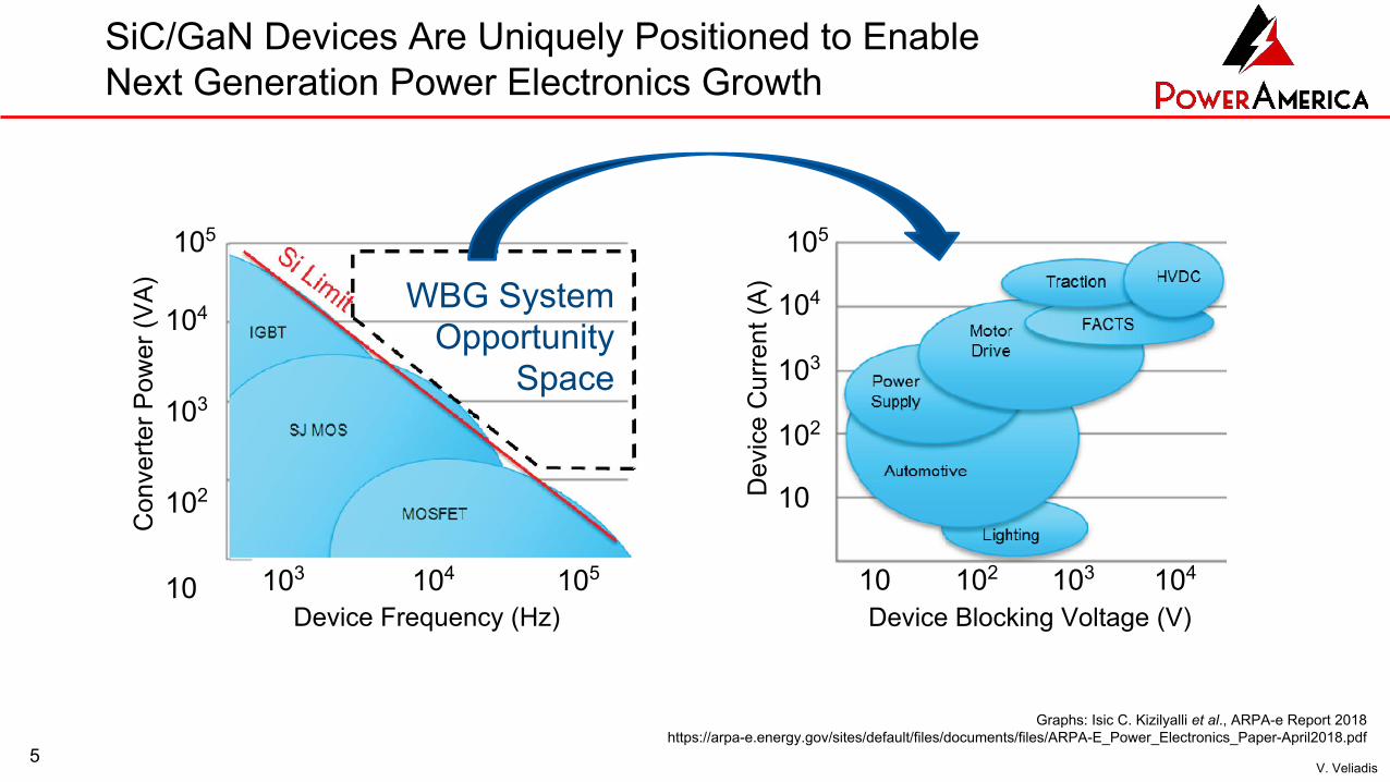
SiC/GaN Devices Are Uniquely Positioned to Enable Next Generation Power Electronics Growth
103 104 105
Con
verte
r Pow
er (V
A) WBG System
Opportunity Space
Device Frequency (Hz)
105
104
103
102
10
Dev
ice
Cur
rent
(A)
105
104
103
102
10
Device Blocking Voltage (V)10 102 103 104
Graphs: Isic C. Kizilyalli et al., ARPA-e Report 2018https://arpa-e.energy.gov/sites/default/files/documents/files/ARPA-E_Power_Electronics_Paper-April2018.pdf
V. Veliadis5
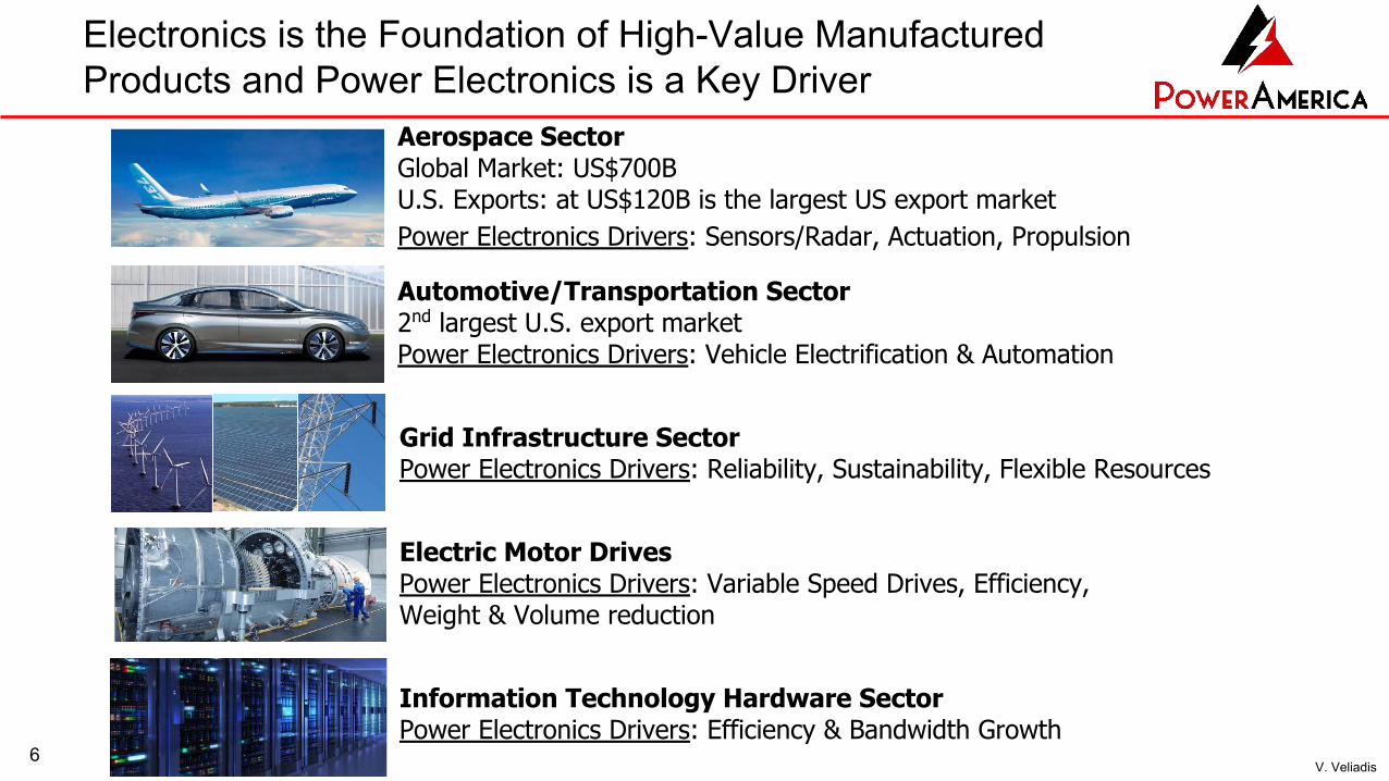
Aerospace SectorGlobal Market: US$700B U.S. Exports: at US$120B is the largest US export marketPower Electronics Drivers: Sensors/Radar, Actuation, Propulsion
Automotive/Transportation Sector2nd largest U.S. export marketPower Electronics Drivers: Vehicle Electrification & Automation
Grid Infrastructure SectorPower Electronics Drivers: Reliability, Sustainability, Flexible Resources
Information Technology Hardware SectorPower Electronics Drivers: Efficiency & Bandwidth Growth
Electronics is the Foundation of High-Value Manufactured Products and Power Electronics is a Key Driver
Electric Motor DrivesPower Electronics Drivers: Variable Speed Drives, Efficiency, Weight & Volume reduction
V. Veliadis6

“More Electric Aerospace” is Primarily an Evolutionary Application of Power Electronics and Energy Storage
Power electronics innovations drive aerospace – aircraft, satellites, drones, rovers
A more electric aircraft is a more energy efficient aircraft• Replace hydraulic systems with
electrical: lower fluid leak hazard, lower operation/maintenance cost, lower system complexity, higher reliability
• Electrical generation/distribution systems replace electromechanical relays, pneumatics, and hydraulics: reduce aircraft wiring and overall weight for fuel savings
• Increased power electronics density: reduces aircraft weight for fuel savings
Better fuel efficiency, lower maintenance/operation costs,
higher reliability, less noise, lower NOx emissions
V. Veliadis7

Power Electronics is Increasingly Prevalent in Hybrid/Electric Vehicles
Source: SDRIVE, “Electrical and electronics technical team roadmap”
V. Veliadis8
In 2014 >25% of all energy usage in the U.S. was consumed in transportation, 98% of that came from fossil fuels

Electric/Hybrid Vehicle Adoption of SiC Power Electronics is Happening Now
V. Veliadis9
• Tesla Model 3 main inverter, features 24 SiC MOSFET modules from ST Microelectronics
https://www.pntpower.com/tesla-model-3-powered-by-st-microelectronics-sic-mosfets/
D. Han, S. Li, W. Lee and B. Sarlioglu, "Adoption of wide bandgap technology in hybrid/electric vehicles-opportunities and challenges," in Proc. IEEE Transportation Electrific. Conf. Expo (ITEC), Chicago, IL, 2017, pp. 561-566
• Review of the WBG devices and their adoption in EVs and HEVs:
• 2014, Toyota, in collaboration with Denso, introduced a prototype SiC power control unit for its Prius HEV, which demonstrated a 5% improvement in the fuel economy over the standard JC08 Japanese drive cycle
http://newsroom.toyota.co.jp/en/detail/2656842

Advances in Power Electronics and Control Systems Drive Efficient, Flexible, and Reliable Grid
Currently, ~40% of generated electric power passes through Power Electronics between generation and use
• HVDC Interface
• FACTS
• Microgrids
• Solar Interface
• Wind Interface (500 GW installed)
• Energy Storage Interface
Electric Grid Applications
V. Veliadis10

Variable Speed Drives Enable Efficient Adaptation to Motor Speed/Torque and Reduce Energy Consumption
Across all sectors, electric motors account for approximately 40% of total U.S. electricity demand
4.16 kV3 phase60 Hz
13.8 kV3 phase60 Hz
1-50 MW60 Hz Motor
CompressorFixed Speed
Big60 HzTransformer
GearBox
Traditional Motor Drives: 20-40% of energy is wasted with throttles and other mechanical devices
https://arpa-e.energy.gov/sites/default/files/documents/files/ARPA-E_Power_Electronics_Paper-April2018.pdf
V. Veliadis11

SiC Based Variable Speed Drives have Volume, Weight, and Cost Advantages
Si based VSD save energy but have limited adoption due to big footprint, weight, and cost
• Big 60 Hz Transformer replaced by small high frequency Transformer • VSD system is reduced in size & weight and cheaper due to WBG devices • Gear Box eliminated • Motor size reduced by 5x – cheaper, less magnets
SiC based VSD use novel architectures to reduce volume, weight and cost, accelerating adoption
US Department of Energy (DOE), Next Generation of Electric Machines ProgramV. Veliadis
12

The Range International Information Group Data Centerin Langfang China is 6.3 Million Square Feet in Area
Data Center power consumption is projected to reach 10% of the total electrical power consumption by 2020
360,000 servers
V. Veliadis13
Waste Heat Management is
Challenging!
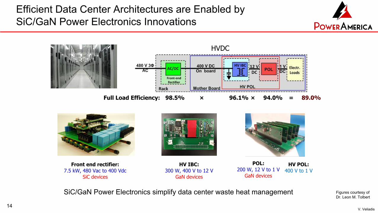
Efficient Data Center Architectures are Enabled by SiC/GaN Power Electronics Innovations
Full Load Efficiency: 98.5% 96.1% 94.0%× × = 89.0%
Front end rectifier: 7.5 kW, 480 Vac to 400 Vdc
SiC devices
HV IBC:300 W, 400 V to 12 V
GaN devices
POL:200 W, 12 V to 1 V
GaN devices
Figures courtesy of Dr. Leon M. Tolbert
HV POL:400 V to 1 V
HVDC
SiC/GaN Power Electronics simplify data center waste heat management
V. Veliadis14
PowerAmerica is Accelerating Adoption of WBG Power Electronics
• The U.S Department of Energy launched the PowerAmerica Manufacturing Institute to Accelerate Adoption of Wide Band Gap power electronics.
• PowerAmerica started operations in 2015 with $140M funds over 5 years, and is managed by North Carolina State University in Raleigh, NC USA.
• PowerAmerica addresses gaps in WBG power technology to enable US manufacturing job creation and energy savings.
V. Veliadis

PowerAmerica is Member Driven and Active in All Areas of the Power GaN-SiC Supply Chain
SiC Foundry
Gov. Labs Consortia
SiC Devices Circuits & Modules
WBG Systems
Aca
dem
ic
GaN Devices & Circuits
V. Veliadis

GaN Device Projected Revenue by 2022: $450M/Yr
V. Veliadis
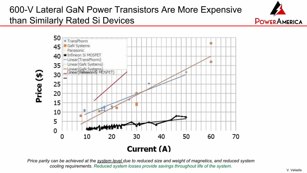
600-V Lateral GaN Power Transistors Are More Expensive than Similarly Rated Si Devices
V. Veliadis
Price parity can be achieved at the system level due to reduced size and weight of magnetics, and reduced system cooling requirements. Reduced system losses provide savings throughout life of the system.
PFC/PS
EV/HEV
xEV Charging
PV
Motor DriveUPS
Rail
Wind
Other
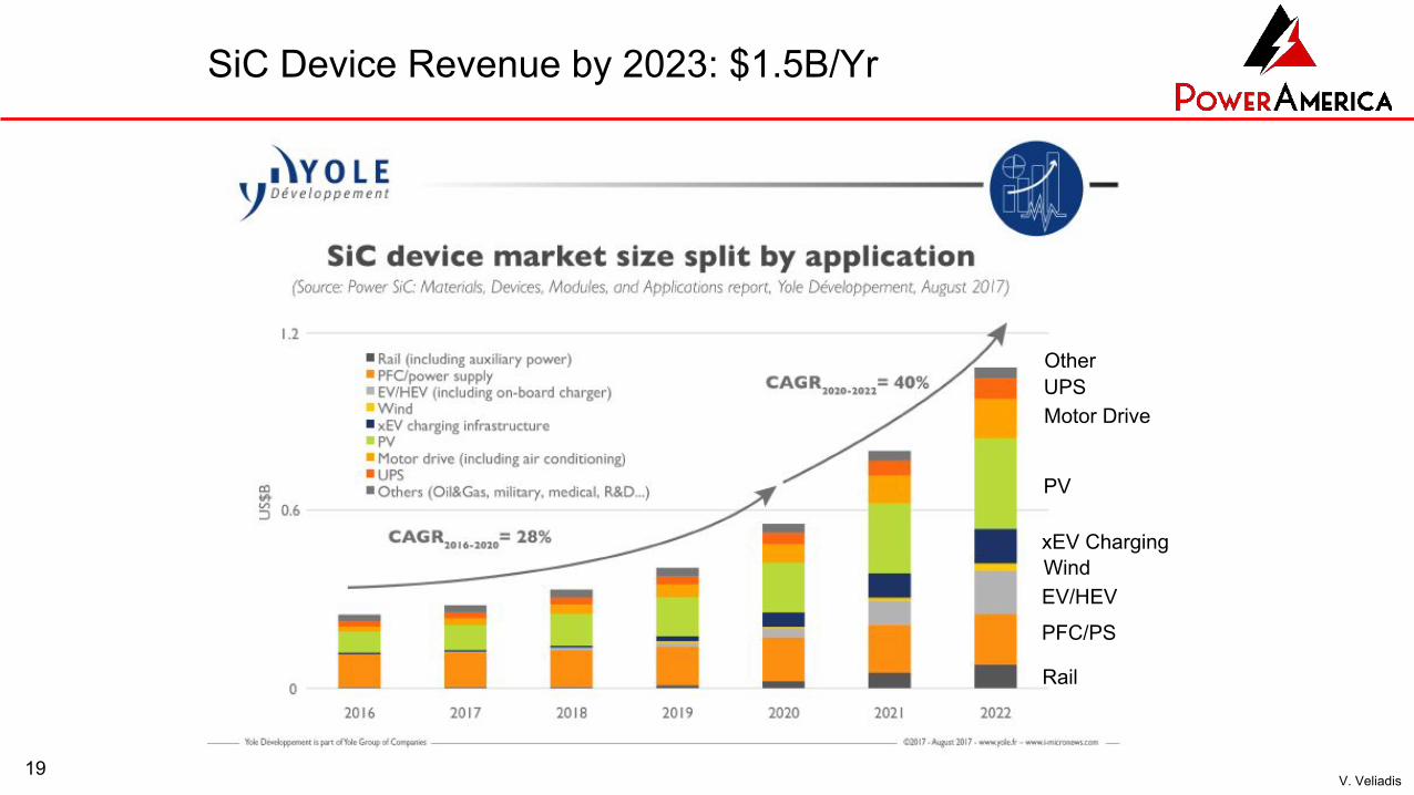
SiC Device Revenue by 2023: $1.5B/Yr
V. Veliadis19
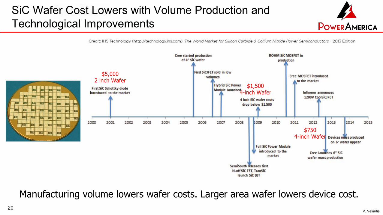
$5,0002 inch Wafer
$1,5004-inch Wafer
$7504-inch Wafer
SiC Wafer Cost Lowers with Volume Production and Technological Improvements
Manufacturing volume lowers wafer costs. Larger area wafer lowers device cost.
V. Veliadis20

Manufacturing Volume, Larger Wafer Area, and Technological Innovations Drive SiC Device Cost Reductions
Normalized area: 1 1.8 4
Graph: Wolfspeed, 2014
V. Veliadis21

1200-V SiC MOSFETs Are More Expensive Than Similarly Rated Si Devices
1200 V
www.digikey.com, Oct. 2017
V. Veliadis22
Price parity can be achieved at the system level due to reduced size and weight of magnetics, and reduced system cooling requirements. Reduced system losses provide savings throughout life of the system.

value
SiC MOSFETs Can Reduce System Cost (and Size) Despite Their Higher Than Si Price
Courtesy:Dr. Levett, Infineon
At 5kW Power
20KHz100KHz
PV Reduction of system cost and size with SiC
› 10-15% lower BOM› 2-3x higher semiconductor costs
Total system cost [US$]
Si-based solution
SiC-based solution
other
(e.g.
magnetics, housing,
etc)
other
semi- conductor
semi- conductor
V. Veliadis23

SiC Wafer Demand Explodes in Anticipation of High Volume Adoption
V. Veliadis24
• Cree, Inc. Announces Long-Term Silicon Carbide Wafer Supply Agreement with Infineon2/26/2018The agreement governs Cree’s supply of advanced 150 mm SiC wafers to Infineon, valued at well over $100 million.https://www.wolfspeed.com/news/cree-inc-announces-long-term-silicon-carbide-wafer-supply-agreement-with-infineon
• Cree and STMicroelectronics Announce Multi-Year Silicon Carbide Wafer Supply Agreement, 1/7/2019
The agreement governs the supply of $250 million dollars of Cree’s advanced 150mm silicon carbide bare and epitaxial wafers to STMicroelectronics during this period of extraordinary growth and demand for silicon carbide power devices.https://www.wolfspeed.com/news/cree-announces-quarter-billion-dollar-wafer-supply-agreement-with-stmicroelectronics
• Cree, Inc. (Nasdaq: CREE) announces that it signed a strategic long-term agreement to produce and supply its Wolfspeed(R) silicon carbide wafers to one of the world's leading power device companies. The agreement, valued at more than $85 million, governs Cree's supply of advanced 150 mm silicon carbide bare and epitaxial wafers, 10/16/18
https://www.cree.com/news-events/news/article/cree-announces-long-term-silicon-carbide-wafer-supply-agreement-with- leading-global-semiconductor-company

PowerAmerica is a Catalyst in the Manufacturing of Low Cost SiC and GaN Power Electronics
Lowers Cost of Devices and Power Electronics
Large Volume Manufacturing
Streamline Fabrication
Demonstrate Compelling System Advantages
Train workforce in WBG
Creates Device Demand
Develop WBG Modules and Circuits, Explore Reliability
Establish Reliability
Improve Material Quality
Large-scale WBG Power Electronics Adoption
Develop Peripheral Technologies
Funding Areas:• Foundry, Devices• Modules, Reliability• Power Electronics Applications• Education
V. Veliadis

DOE/PowerAmerica Strategic Funding Allocation Accelerates Commercialization of WBG Power Electronics
33 NEW WBG Projects
Annually
Industry/Unive
rsity/N
ational-Lab
V. Veliadis

PowerAmerica Foundry Projects Enable Low-Cost Large Volume SiC Device Manufacturing in the U.S.
V. Veliadis

PowerAmerica Supports U.S. SiC Foundry Infrastructure
V. Veliadis
*IDM: Integrated Device Manufacturers
SiC Foundry• Wafer quality/supply• Compete on Processing
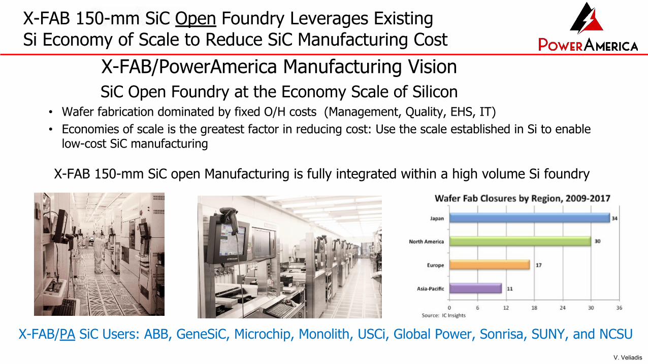
X-FAB 150-mm SiC Open Foundry Leverages Existing Si Economy of Scale to Reduce SiC Manufacturing Cost
X-FAB/PowerAmerica Manufacturing Vision SiC Open Foundry at the Economy Scale of Silicon
X-FAB 150-mm SiC open Manufacturing is fully integrated within a high volume Si foundry
• Wafer fabrication dominated by fixed O/H costs (Management, Quality, EHS, IT)• Economies of scale is the greatest factor in reducing cost: Use the scale established in Si to enable
low-cost SiC manufacturing
X-FAB/PA SiC Users: ABB, GeneSiC, Microchip, Monolith, USCi, Global Power, Sonrisa, SUNY, and NCSUV. Veliadis

TSMC’s Low-Cost Lateral GaN Power Device Production is a Barrier to Establishing an Open Domestic GaN Foundry
30
• TSMC is unmatched by any other foundry, with manufacturing capacity of over 12 million 12-inch equivalent wafers annually as of 2018
• TSMC 2018 revenue of $33.49 billion USD accounts for an enormous 48.1% market share
V. Veliadis
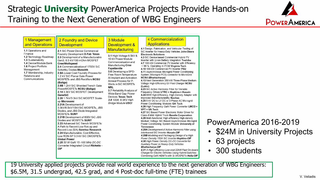
5.1 Education and Workforce Pipeline Development 5.4 Undergraduate Research Scholars5.5 Pre-College Education 5.6 WBG Short Courses5.13 Documentation of Design and Process of GaN Power HEMTs RPI
19 University applied projects provide real world experience to the next generation of WBG Engineers: $6.5M, 31.5 undergrad, 42.5 grad, and 4 Post-doc full-time (FTE) trainees
Strategic University PowerAmerica Projects Provide Hands-on Training to the Next Generation of WBG Engineers
V. Veliadis
PowerAmerica 2016-2019• $24M in University Projects • 63 projects• 300 students

Industry DrivenShort Course Content
SOLD O
UT
2.5 day duration
V. Veliadis
PowerAmerica Wide Band Gap Short Course Trains Existing Workforce

2017-2018 PowerAmerica WBG Tutorial presentations at prestigious conferences:✔ “SiC Processing - An Exercise in Si Fabrication with a High Temperature Twist,” Veliadis 225
attendees, International Conference on SiC and Related Materials ICSCRM Sept. 2017
✔ “SiC power device design and fabrication, and insertion in novel MV Power Converters”, Veliadis and Bhattacharya, 25 attendees, IEEE Energy Conversion and Congress & EXPO (ECCE) Oct. 2017
✔ “SiC power device design and fabrication: making the transition from Silicon,” Veliadis, 160 attendees International Symposium on Power Semiconductor Devices and ICs (ISPSD), May 2018
V. Veliadis
410 Tutorial Attendees in 2017-2018
PowerAmerica Wide Bandgap Conference Tutorials Educate Participants and Promote Mission and Sustainability

• Networking– Summer/Winter member meetings– Summary presentation of all PA projects at meetings– Long networking breaks at meetings
• Access to Universities and Recruitment– Student presentations, internships– Job opportunities posted on website– Collaborative research projects
• Education and Workforce Development– WBG short course offering with industry driven content– Tutorials presented at major WBG conferences
• Timely Access to PowerAmerica Device Bank Engineering samples
• WBG Ecosystem Benefits such as roadmaps, industry perspectives, technical consulting, member initiated projects, and promotion of SiC
and GaN power technology
PowerAmerica Provides Value Beyond DOE Funding and Will Continue to Accelerate WBG Technology Manufacturing

PowerAmerica accelerates WBG commercialization
V. Veliadis

36
0.19 cm2 Area SiC JFET Blocks 1700 V and Outputs 54 A at a Voltage Drop of 2 V
V. Veliadis

Third Party Testing/Reliability Verification: SiC JFET Electrical Characteristics Do Not Degrade after 2.4 million 1200-V Hard-switch Short-circuit Pulses at 150 °C
Blocking voltage JFET curves do not change after 2.4 million 1200-V/115-A
hard-switch pulses at 150 ºC
• Peak current is 115 A: 13 times the JFET’s 250 W/cm2 rated current at 150 °C• Energy dissipated by the JFET during each hard switching event is 73.2 mJ• Peak dissipated power: 68.2 kW • Current rise rate was 166 A/μs and the pulse FWHM was 1.8 µs
Standardized accelerated testing of large volumes of WBG devices will establish their Reliability
V. Veliadis

600-V / 60-A SiC JFET Based Bidirectional Power Switching Demonstrated at 25 °C
Test conditions: • 600-V, 60-A (both directions)• 30˚C liquid cooled heat sink• Approx 20-µH circuit inductance (12-m cabling)
Results:• 60 to 0-A at 600-V in approx. 10-µs• Symmetric bidirectional conduction and turn-off• 300-V overshoot (900-V) peak
Two 30-A modules paralleled for 60-A
conduction
+
10-µs turn-off
V. Veliadis

39
Wafer-scale interconnection approach:• Determine largest discrete device area fabricated at high yield
• Fabricate discrete devices with edge termination
• Test discrete devices on wafer to generate yield wafer-map
• Interconnect good discrete devices across the wafer (Failed devices are not connected)
GREEN: good, RED: failed
Edge exclusion
Wafer-scale Interconnection of High-yielding Devices Maximizes Power per Weight/Volume
Wafer-scale InterconnectionV. Veliadis

Wafer-scale Interconnected PiN Diode Packaged for Pulsed Testing
Wafer-scale Interconnected PiN diode was press-packaged:
• Press pack accommodates ¼, ½, and wafer-scale devices• Centering rings are used to ensure even pressure• Can be pressurized to measure the leakage current in the
diode before and after high current shots
Test-bed developed for wafer-scale diode pulsing:• 3.1 mF Pulse-Forming-Network (PFN) generates
rectangular current pulses• PFN is switched by a Light Activated Semiconductor Switch
or a Spark Gap• Current Pulse Width: 0.5 ms• Current Risetime: 33 μs• Maximum Current: Variable to 96 kA (at 20 kV charge)
V. Veliadis

11.7-cm2 active-area Interconnected 1.8 kV Wafer-scale Diode is Pulsed at 64 kA and Dissipates 382 J
65 kA
Dissipated Energy = 382 JRdiode = 0.13 mΩ (di/dt = 0)Vdiode = 10.3 V (di/dt = 0)
Action = 1.7 MA2-secVcharge = 11 kVdi/dt = 1100 A/µs
Current Density = 5.5 kA/cm2
Capacitance = 3.1 mFPulse Width = 470 µs
V. Veliadis

42
2.6 kV Quarter Wafer Bi-level Interconnected SiC Thyristor Power Switch Demonstrated
FLAT
AnodePad
Gate Pads
V. Veliadis