Embed Size (px)
Citation preview

ABSTRACT
Title of Dissertation: AN ANALYTICAL AND EXPERIMENTAL
INVESTIGATION OF FILAMENT FORMATION IN GLASS/EPOXY COMPOSITES.
Keith Leslie Rogers, Doctor of Philosophy, 2005 Dissertation Directed By: Professor, Michael Pecht, Department of
Mechanical Engineering The drive to increase circuit density with smaller PWB geometries and higher layer
counts in multi-layer boards along with the increasing use of electronics in harsh
environments for high reliability and safety critical applications (automotive,
avionics, medical, military) have made short circuiting of PWBs due to growth of
conductive filaments between biased conductors a major concern. In addition, the
impending implementation of lead-free soldering processing, which may affect
laminate stability and materials choices, can increase the potential for conductive
filament formation (CFF) failures. To mitigate these catastrophic failures, it is
necessary to understand the roles and synergistic effects of environmental conditions,
material properties and manufacturing quality in accelerating or deterring CFF.
In this dissertation, four laminate types (including a halogen free) and three conductor
spacings are tested at different voltages in accordance with IPC TM-650, allowing a
ranking of these laminate types based on resistance to CFF. Demonstrated is the use

of an innovative technique, the superconducting quantum interference device
(SQUID), to verify and locate the internal short circuits due to CFF. The SQUID
which detects magnetic fields generated by the current paths, displays images of the
current density enabling identification of the shorted locations. With this technique, a
new variant of filament formation in glass/epoxy composites: vertical filament
formation (VFF) was identified. The conductive filaments found at the failure sites
were observed during cross-sectioning techniques, verifying that the failures were due
to CFF. A test standard to identify and quantify hollow glass fibers, potential paths
for filament formation in laminated PWBs, was created. It was observed that board
types, which show the longest time to failure due to CFF in PTH-PTH configuration,
might not offer the best protection for PTH-plane geometry. Based on insulation
resistance measurements, it was seen that the IPC-TM-650 test specification of
monitoring every 24 hours could allow intermittent failures to go undetected. It was
demonstrated that PTH-PTH dielectric breakdown voltage values followed the same
trend as the time to failure observed for the PTH-PTH CFF failure data, suggesting
that dielectric breakdown voltage can be an indicator of CFF susceptibility, saving
considerable time and cost.

AN ANALYTICAL AND EXPERIMENTAL INVESTIGATION OF FILAMENT FORMATION IN GLASS/EPOXY COMPOSITES
By
Keith Leslie Rogers
Dissertation submitted to the Faculty of the Graduate School of the University of Maryland, College Park, in partial fulfillment
of the requirements for the degree of Doctor of Philosophy
2005 Advisory Committee: Professor Michael Pecht, Chair Professor David Barbe Professor Donald Barker Professor Patrick McCluskey Professor Omar Rahami

© Copyright by Keith Leslie Rogers
2004

ii
ACKNOWLEDGEMENTS
I first want to give thanks and praise to the Almighty God for His blessings in my life,
especially during my college years. I also want to doubly thank my parents for
exemplifying what perfect role models should be, and for their unwavering support
and encouragement.
I want to thank my dear wife - Dilcia Rogers and my two wonderful sons - Keith
Rogers Jr. and Kurtis Rogers for allowing me to take time away from them to
complete this dissertation.
I would like to thank my advisor Professor Michael Pecht for his assistance, guidance
and constructive criticism during my graduate studies. I am also indebted to him for
opening many doors that would have other wise been barred to me. My
acknowledgements to the other members of my advisory committee, Professors
Patrick McCluskey, Omar Rahami, David Barbe and Donald Barker. I especially
thank Dr. Craig Hillman for his assistance with the overall project.
Lastly, I want to thanks all the wonderful people at CALCE for their help, support,
and for making our laboratories enjoyable places to work.

iii
TABLE OF CONTENTS
Acknowledgements....................................................................................................... ii Table of Contents......................................................................................................... iii List of Figures ............................................................................................................... v Chapter 1: Introduction ................................................................................................. 1
1.1 Electrically Induced Failures in Printed Wiring Boards ..................................... 1 1.2 Electrochemical Migration.................................................................................. 2 1.3 Motivation........................................................................................................... 6
Chapter 2: Background ................................................................................................. 8 2.1 Previous Studies.................................................................................................. 8
2.1.1 Bell Laboratories, 1955......................................................................... 8 2.1.2 Lathi, 1979 ............................................................................................ 9 2.1.3 Lando, 1979 ........................................................................................ 10 2.1.4 Welsher, 1980 ..................................................................................... 12 2.1.5 Mitchel, 1981 ...................................................................................... 12 2.1.6 Augis, 1989......................................................................................... 13 2.1.7 Rudra, 1994......................................................................................... 15 2.1.8 Ready, 1996 ........................................................................................ 15 2.1.9 Turbini, 2000....................................................................................... 16 2.1.10 Sauter, 2002 ........................................................................................ 17 2.1.11 National Physical Laboratory, 2004 ................................................... 18
2.2 Numerical Models to Predict CAF Formation.................................................. 20 2.2.1 Welsher CAF Models ......................................................................... 20 2.2.2 Mitchell CAF Model........................................................................... 21 2.2.3 Augis CAF Model............................................................................... 22 2.2.4 Rudra CALCE CFF Model ................................................................. 22 2.2.5 Li Modified CALCE CFF Model ....................................................... 23 2.2.6 Sun Microsystem’s Model (Based on CALCE).................................. 24
Chapter 3: PWB Manufacturing ................................................................................. 25 3.1 Glass Fibers....................................................................................................... 25 3.2 Production of Fiber Weaves.............................................................................. 27 3.3 Lamination ........................................................................................................ 28 3.4 Hole Drilling ..................................................................................................... 29 3.5 Surface Finishes ................................................................................................ 30 3.6 Defects that may Initiate and Accelerate CFF Failures .................................... 33 3.7 Summary ........................................................................................................... 38
Chapter 4: Hollow Fiber Detection............................................................................. 39 4.1 Introduction....................................................................................................... 39 4.2 Measurement Techniques for Hollow Fibers in Common Laminates .............. 39 4.3 Discussion of the Hollow Glass Fiber Problem................................................ 45 4.4 Failure Opportunities due to Hollow Fibers ..................................................... 47
Chapter 5: Analyzing CAF Failures ........................................................................... 52 5.1 Electrical Testing .............................................................................................. 52 5.2 Thermal Imaging............................................................................................... 53

iv
5.3 Superconducting Quantum Interference Device............................................... 55 Chapter 6: CFF Experiments ...................................................................................... 58
6.1 Test Board Design............................................................................................. 58 6.2 Test Procedure .................................................................................................. 61 6.3 Experimental Testing ........................................................................................ 68
6.3.1 Insulation Resistance Monitoring .............................................................. 69 6.4 Failure Analysis ................................................................................................ 78 6.5 Dielectric Breakdown ....................................................................................... 83
Chapter 7: Path Formation .......................................................................................... 87 7.1 Modes of Path Formation.................................................................................. 88
7.1.1 Mechanical Degradation ..................................................................... 88 7.1.2 Chemical Degradation ........................................................................ 89 7.1.3 Hollow Fibers...................................................................................... 89 7.1.4 Vertical Filament Formation............................................................... 90
7.2 Use of SQUID Microscopy in Detecting VFF.................................................. 96 Chapter 8: Glass-Silane-Epoxy Bonding and Debonding .......................................... 97
8.1 Voltage Dependency of Glass-Epoxy Interfacial Adhesion ............................. 97 8.2 Chemistry of Glass-Silane-Epoxy Interfacial Bonding .................................. 100
Chapter 9: Observations and Contributions.............................................................. 108 9.1 Observations ................................................................................................... 108 9.2 Contributions................................................................................................... 110
Chapter 10: Summary ............................................................................................... 112 Chapter 11: Future Work .......................................................................................... 116 References................................................................................................................. 118
v
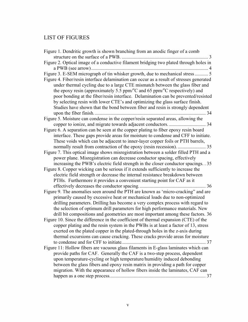
LIST OF FIGURES
Figure 1. Dendritic growth is shown branching from an anodic finger of a comb structure on the surface of a PWB. ....................................................................... 3
Figure 2. Optical image of a conductive filament bridging two plated through holes in a PWB (see arrow) ................................................................................................ 4
Figure 3. E-SEM micrograph of tin whisker growth, due to mechanical stress ........... 5 Figure 4. Fiber/resin interface delamination can occur as a result of stresses generated
under thermal cycling due to a large CTE mismatch between the glass fiber and the epoxy resin (approximately 5.5 ppm/oC and 65 ppm/oC respectively) and poor bonding at the fiber/resin interface. Delamination can be prevented/resisted by selecting resin with lower CTE’s and optimizing the glass surface finish. Studies have shown that the bond between fiber and resin is strongly dependent upon the fiber finish. ........................................................................................... 34
Figure 5. Moisture can condense in the copper/resin separated areas, allowing the copper to ionize, and migrate towards adjacent conductors. .............................. 34
Figure 6. A separation can be seen at the copper plating to fiber epoxy resin board interface. These gaps provide areas for moisture to condense and CFF to initiate. These voids which can be adjacent to inner-layer copper foils or PTH barrels, normally result from contraction of the epoxy (resin recession). ....................... 35
Figure 7. This optical image shows misregistration between a solder filled PTH and a power plane. Misregistration can decrease conductor spacing, effectively increasing the PWB’s electric field strength in the closer conductor spacings. . 35
Figure 8. Copper wicking can be serious if it extends sufficiently to increase the electric field strength or decrease the internal resistance breakdown between PTHs. Furthermore it provides a convenient starting point for CAF as it effectively decreases the conductor spacing. ...................................................... 36
Figure 9. The anomalies seen around the PTH are known as ‘micro-cracking” and are primarily caused by excessive heat or mechanical loads due to non-optimized drilling parameters. Drilling has become a very complex process with regard to the selection of optimum drill parameters for high performance materials. New drill bit compositions and geometries are most important among these factors. 36
Figure 10. Since the difference in the coefficient of thermal expansion (CTE) of the copper plating and the resin system in the PWBs is at least a factor of 13, stress exerted on the plated copper in the plated-through holes in the z-axis during thermal excursions can cause cracking. These cracks provide areas for moisture to condense and for CFF to initiate..................................................................... 37
Figure 11: Hollow fibers are vacuous glass filaments in E-glass laminates which can provide paths for CAF. Generally the CAF is a two-step process, dependent upon temperature-cycling or high temperature/humidity induced debonding between the glass fibers and epoxy resin matrix in providing a path for copper migration. With the appearance of hollow fibers inside the laminates, CAF can happen as a one step process............................................................................... 37

vi
Figure 12. This photo shows the diagonal sections (black dot in middle) that are used for the hollow fiber assessments. By using only the sections on the diagonal, ensues that each hollow fiber is not accounted for more than once.................... 40
Figure 13. Placing the copper cladded laminates in a chemical solution of concentrated hydrochloric and nitric acid (aqua regia), for about 10 to 15 minutes, effectively removes all exposed copper from the surfaces. This is done in a fume hood, using the appropriate protection necessary for working with hazardous chemicals. .......................................................................................... 40
Figure 14. Photo showing before and after resin removal .......................................... 41 Figure 15. Light travels freely until it hits a hollow fiber (air). The change in
refractive index at the fiber/air boundary partially reflects it. ............................ 43 Figure 16. A change in the refractive properties is evident through an optical
microscope by a bright white line. In some cases, a hollow fiber could be detected without using a microscope. The light source is positioned so that light enters the edge of the fabric perpendicular to the fibers being observed............ 43
Figure 17. Although hollow fibers are visible to the naked eye (see arrows), a microscope attachment is best to view them....................................................... 44
Figure 18. The edges of this sample were not dipped in wax. As the sample was submerged in oil, the oil started to flow into one of the hollow fibers. A mark was set at one point of the hollow fiber so that the movement of the oil could be more easily visualized. Only the hollow fiber is visible, due to the exact match between the refractive index of the oil and the fiber glass. ................................ 44
Figure 19. Hollow fibers can be seen as white lines traveling along the fiber bundle weave in these pictures. The refractive index of E-glass is 1.550, while that of the oil used here is 1.553. This difference of 0.003, allows the fabric weave to also be seen. ........................................................................................................ 45
Figure 20. Hollow fibers are vacuous glass filaments in E-glass laminates which can provide paths for conductive filament formation (CFF). Generally the CFF is a two-step process, dependent upon temperature-cycling and humidity-cycling induced debonding between the glass fibers and epoxy resin matrix to provide a path for copper migration. With the appearance of hollow fibers inside the laminates, CFF can happen as a one step process............................................... 46
Figure 21. This drawing shows the PTH grid, PTH diameter (d) and the planar surface dimensions of each cell (G x G) in the PTH grid. .............................................. 48
Figure 22. This E-SEM photo shows a cross-section of a printed circuit board containing two PTHs, resin and woven fiber glass............................................. 48
Figure 23. For a 37 x 69 grid of PTHs, where x = 37 PTH rows and y = 69 columns in the grid, the number of possible adjacent PTH failure sites can be calculated by: (37+68)(69+36) = 5,000 possible failure sites. In a square grid, where x = y, this simplifies to 2[x(x-1)] or ~2x2 for x > 100. ........................................................ 50
Figure 24. This PWB section (half of board used by AVICI Systems) contains close to 7,000 PTHs. On the Fujitsu M-780 large-scale general purpose computer, there are more than 80,000 PTHs per circuit card. ............................................. 51
Figure 25. Conductor geometry of shorted adjacent PTHs where electrical testing could verify an internal short in a PWB, after isolation from the rest of the circuitry (removal of the surface traces) is removed is shown. .......................... 53

vii
Figure 26. The photo at the top shows the thermal imaging equipment, while the photo at the bottom shows a sequential series of snapshots (clockwise starting at top left) as the power is turned on, identifying the shorted area......................... 54
Figure 27. After locating the area by thermal imaging, cross-sectional techniques verified that there was an internal short between a PTH and ground plane. ...... 54
Figure 28. Photo of the superconducting quantum interference device equipment.... 55 Figure 29. SQUID current mapping technique used to locate short circuit between
planes in a PWB.................................................................................................. 56 Figure 30. An optical image shows the shorted site located between two planes, after
cross-sectioning based on the SQUID results..................................................... 56 Figure 31. Design of the CFF test board used in this study........................................ 58 Figure 32. The photos in A and B give examples of the PTH-PTH and PTH-plane
conductor geometry features respectively. ......................................................... 59 Figure 33. Optical dark field photo showing a cross-section of the test board’s internal
layer stack up ...................................................................................................... 60 Figure 34. Photo shows the test board with the PTH-PTH grid and the PTH-internal
plane test patterns................................................................................................ 61 Figure 35. Photo of the boards hanging in the environmental chamber, parallel to the
air flow and spaced approximately 2 inches apart. ............................................. 62 Figure 36. Monitoring and plotting system used to check variations in temperature
and humidity settings. ......................................................................................... 63 Figure 37. Block diagram of equipment setup to monitor insulation resistance ........ 63 Figure 38. Schematic of the electrical circuitry used for monitoring the insulation
resistance............................................................................................................. 64 Figure 39. The normal current path is shown in red, going through a shorting box... 65 Figure 40. The current path, shown in red, obtained by “opening” the shorting box,
was used when a device was being tested........................................................... 65 Figure 41. Light colored wires were used for the positive connections (yellow and
white) while the darker colored wires (purple and blue) were used for the negative connections. This nomenclature helped to avoid polarity mix-ups...... 67
Figure 42. Moisture absorption characteristics for the four board types exposed to 85oC/85% RH for 700 hours is shown................................................................ 68
Figure 43. Plot of the PTH-PTH insulation resistance for the 20 samples exposed to 85oC/85% RH at a 10-volt bias........................................................................... 69
Figure 44. Plot showing PTH-PTH intermittent nature of the failures....................... 70 Figure 45. Intermitent failures can last for less than 6 minutes. Monitoring every 24
hours according to IPC-TM-650 specifications may not catch these short duration failures. ................................................................................................. 70
Figure 46. Plot showing internal resistance of the PTH-plane in the powered samples. Isola samples, IS 70A and IS 70C, failed between 30 and 130 hours. The missing data section was due to a power outage. ............................................................. 73
Figure 47. Plots of the resistance in the PTH-plane show intermittent behavior. ...... 73 Figure 48. Close to the end of the 50-volt testing of the PTH-plane circuitry, 8
surviving samples can be seen above the lines above 1E8 ohms. ...................... 74 Figure 49. This plot shows the insulation resistance monitored at 100 volts for the
duration of 500 hours. Some of the samples did not fail. ................................... 76

viii
Figure 50. This plot shows the insulation resistance for the PTH-PTH XG samples up to 40 hours, at which time all had failed............................................................. 76
Figure 51. The SQUID output shows the current mapping images, verifying that there were short circuits and determining their locations respective to the board conductors. .......................................................................................................... 78
Figure 52. SQUID mapping and respective conductor locations for cross-sectioning.............................................................................................................................. 79
Figure 53. Prior to reaching the failure site, circular black blue areas, possibly Cu(OH)2 due to reaction with water were observed. .......................................... 79
Figure 54. A filament was observed bridging two PTH, at the same location predicted by the SQUID (see red arrow). ........................................................................... 80
Figure 55. This optical micrograph shows an enlargement of the shorted site........... 81 Figure 56. This current mapping of one of the failed XG samples at the PTH-PTH
grid show that the current follows the grid pattern, and contains many leakage paths; not one as in the CFF validated failures. It is possible that these were the same type of early failures in the AF samples as well........................................ 81
Figure 57. This optical photo shows a copper filament bridging a PTH and ground plane at the precise location predicted by the SQUID........................................ 82
Figure 58. An EDS analysis of a cross-sectioned site perpendicular to the filament showed copper in the shorted location................................................................ 82
Figure 59. E-SEM inspection revealed delamination at the fiber-epoxy interfaces in areas immediately surrounding the failure site. .................................................. 83
Figure 60. Photos show the damage to the PTH as a result of the dielectric breakdown testing.................................................................................................................. 85
Figure 61. Three common CFF pathway configurations ............................................ 87 Figure 62. Optical micrograph, under brightfield lighting, of a void observed during
cross sectioning of a board.................................................................................. 91 Figure 63. Optical micrograph, using differential interference contrast, of a vertical
cross-section of the board. The filler agglomerate has maximum dimension of 3.5 mil (87 microns). A yellow arrow marks what appear to be nodules of copper emanating from layer 10 (power). ...................................................................... 92
Figure 64. Optical micrograph of a vertical cross-section showing what appears to be a nodule in the PWB. .......................................................................................... 93
Figure 65. Particle observed in the center of a “mound”............................................ 94 Figure 66. Area containing a particle bridging two copper planes shown.................. 95 Figure 67. Particle seen in material bridging two copper planes. ............................... 96 Figure 68. Schematic of reaction between organosilane and glass surface ................ 99
1
CHAPTER 1: INTRODUCTION
1.1 Electrically Induced Failures in Printed Wiring Boards
Conductive filament formation (CFF) also known as metallic electromigration and
conductive anodic filamentation (CAF), is a failure observed within the bulk of glass-
reinforced epoxy printed wiring board (PWB) laminates. This phenomenon is an
electrochemical process involving the transport, usually ionically, of a metal through
or across a nonmetallic medium under the influence of an applied electric field. The
growth of the metallic filament is a function of temperature, humidity, voltage,
laminate materials, manufacturing processes and the geometry and spacing of the
conductors. The growth of these filaments can cause an abrupt, unpredictable loss of
insulation resistance between the conductors under a DC voltage bias.
This failure mode was first observed at Bell Laboratories located in Whippany, New
Jersey, in 1976 [1]. However, more recently there has been an increase in reliability
concerns due to CAF failures. Three of the driving forces behind these reliability
concerns are:
1. The trend toward more compact and lighter electronic devices using smaller
PWBs geometries and multi-layered boards
2. The increase in use of electronic products for high reliability and safety
critical applications (avionics, automotive, medical and military) in harsh
environments
2
3. The higher board processing temperatures, due to the implementation of lead-
free electronics, can affect laminate stability and limit material choices
These factors have increased the focus on conductive filament formation and resulted
in testing standards such as IPC-TM-650-2.6.25 (Conductive Anodic Filament
Resistance Test), the fabrication of CAF resistant laminates and companies annually
spending millions of dollars on research to gain a more in-depth understanding of
CAF failures.
1.2 Electrochemical Migration
Electrochemical migration may be defined as the growth of conductive metal
filaments in a printed wiring board (PWB) under the influence of a direct current
voltage bias. This may occur on an external surface, or through the bulk of a
composite material (e.g., glass fiber/epoxy resin laminate) [2]. Growth occurs by
electro-deposition from a solution containing metal ions. These ions are dissolved at
one conductor, transported by the electric field and re-deposited at the other
(oppositely biased) conductor.
Two distinct electrochemical migration phenomena can occur in PWBs. In the first
case, surface dendrites have been observed to form from the cathode to the anode
under an applied voltage when surface contaminants and moisture are present (see
Figure 1). If the voltage bias is sufficiently high, the dendrites bridging the gap
between the anode and the cathode may “blow-out” (similar to a fuse), leaving

3
sludge-like debris on the surface. These filaments are fragile and may be destroyed by
oxidation, changes in surface tension during moisture absorption, drying, cooling or
heating, or blown-out if the current is sufficient. Short circuits therefore tend to be
intermittent, but filaments can reform.
Figure 1. Dendritic growth is shown branching from a cathodic finger of a comb structure on the surface of a PWB. The second form of electrochemical migration and the focus of this dissertation is
conductive filament formation (CFF), also referred to as conductive anodic filament
(CAF) formation (see Figure 2). CFF differs from the surface dendritic growth in a
number of ways:
• In CFF, the migrating metal is usually copper, as opposed to tin or lead in
dentritic growth.

4
• In CFF, the direction of the filament growth (in the case of copper conductors)
is from the anode to the cathode, not from the cathode to the anode as
observed in dendritic growth.
• In CFF, the filament is composed of a metallic salt, not neutral metal atoms as
in dendritic growth.
• In CFF, the phenomenon occurs internally, not on the surface or superficially
as in dendritic growth.
Figure 2. Optical image of a conductive filament bridging two plated through holes in a PWB (see arrow) Electrochemical migration should not be confused with whisker growth, which is
induced by mechanical stress, and not electrically driven (see Figure 3).

5
CFF failures have three distinct signatures:
1 Intermittent short circuiting - in this case, the conductive filament bridging the
two shorted conductors blows out due to the high current in the filament (similar
to a fuse), but can reform again. These tend to be diagnosed as no fault detected
(NFD) or cannot duplicate (CND) failures.
Figure 3. E-SEM micrograph of tin whisker growth, due to mechanical stress
2 Conductive filaments fully or partially bridging conductors – these typically occur
in current limiting accelerated tests where once a short circuit is formed, the

6
current is limited by a resistor in series with the applied voltage, preventing
burnout and preserving the conductive filament.
3 Burnt or charred areas between shorted conductors - most of the field failures
display this failure signature; internal shorting characterized by a dark charred
epoxy resin/glass fiber area, between and often connecting the conductors
involved.
1.3 Motivation
Laminates are found in almost all electronics products (organic printed boards make
up over 90% - standard FR-4 represents 85% of the resin systems of the present types
of interconnecting substrates). If an electrical short occurs in a printed wiring board
(PWB), there is a potential for the entire system to fail.
A comparison of the failures investigated by the CALCE Failure Analysis Laboratory
shows that 26% of the failures were PWB related. From this population, failure
analyses to determine a root-cause showed that a significant number of the failures
were due to CFF.
As PWBs continue to increase in density by using tighter pitches as well as thinner,
single-ply dielectrics coupled with higher voltages and higher processing
temperatures (resulting from the use of lead-free solder), the potential for CFF-caused
failures will also continue to increase. Hence to prevent these types of catastrophic
failures, it is necessary to understand the roles and synergistic effects of environ-

7
mental conditions, material properties and manufacturing quality in accelerating or
deterring CFF.

8
CHAPTER 2: BACKGROUND
2.1 Previous Studies
2.1.1 Bell Laboratories, 1955
Researchers from Bell Laboratories in 1955 observed that silver in contact with
insulating materials under an applied electrical bias can be ionically removed from its
initial location at an anode and be re-deposited as metal at a different location at a
cathode [3]. A major requirement for the process is the adsorption of water on the
insulating surface to act as the electrolyte. Examination of the metal re-deposited at
the cathode revealed a dendritic structure, while the deposits at the anode appeared
brownish and colloidal. Since silver was the only metal at that time to cause a
potential hazard, the process was called silver migration. Parameters which were
identified as affecting the silver migration rate were; the properties of the insulating
material, the DC voltage, time of the voltage application and the percent relative
humidity. Phenol fabric, the insulating material between the metals was found to be
susceptible to silver migration. The rate of the migration was observed to increase
with voltage and relative humidity. Mitigation techniques suggested included resin
impregnation to more effectively isolate fibers, pretreatments of fibrous surfaces with
water repellant agents and the use of silver precipitating agents to capture free silver
ions.

9
2.1.2 Lathi, 1979
In 1979, Lahti et al. [4] conducted experiments on configurations of single sided,
double sided and multilayered rigid PWBs with and without plated-through-holes
(PTHs) with conductor spacings ranging from 5 mils to 50 mils, temperatures from
23o C to 95o C, relative humidities from 2% to 95% and test voltages ranging from
10V to 600V. They observed that while monitoring CAF failures, there is little or no
degradation in insulation resistance up to the point of failure. Hence, prior to failure,
is it difficult to anticipate or predict failure by examining or monitoring insulation
resistance. Also seen was that the mechanism responsible for CAF failures involves
the penetration of the glass/epoxy interface by a conductive copper compound
generated by electrochemical activity at the anodically biased conductors. The first
indication that the mechanism has initiated is the visual enhancement of the glass
reinforcement around the anodes due to the physical separation at the glass/epoxy
interface. Dark copper-bearing material then begins to fill the articulated regions,
growing away from the anodes. The growth of the copper-bearing material follows
the reinforcement in many directions, but ultimately preferentially towards the
cathodically biased conductors. The researchers observed that at spacings less than 5
mils, failure times dropped drastically. Lot to lot variability in the CAF resistance of
the epoxy-glass printed wiring boards was also noted; one lot may perform better at
400V than another set at 45V. No substantial differences were noted in testing
materials manufactured five years ago, compared to, at that time, currently
manufactured laminates. Among the variables observed to affect the susceptibility of
a PWB to CAF, the most important appeared to be raw materials. Processing factors

10
such as process chemistry and lamination parameters in addition to assembly
parameters such as fluxing, soldering, cleaning and baking were shown to influence
the propensity of a PWB to CAF failure. From the tests, it was concluded that the
CAF failure mechanism is voltage sensitive, but not highly so; the dependence was
not found to be greater than 1/V. In this study, failures occurred first on the most
deeply buried layers and later in the layers closer to the board surface.
2.1.3 Lando, 1979
Lando et al. [5] in 1979 proposed a two-step model to explain the growth of the
conductive filaments occurring at the resin-glass interface in PWBs. The first step is
the degradation of the resin-glass interfacial bond followed by a second step, the
electrochemical reaction. According to Lando’s hypothesis, the path required for the
transportation of metal ions, formed by the degradation of the resin-glass interfacial
bond, may result from mechanical release of stresses, poor glass treatment, hydrolysis
of the silane glass finish or stresses resulting from moisture induced swelling of the
epoxy resin. The path formation was reported to be bias independent, but possibly
humidity sensitive, in the case of chemical degradation. After path formation, the
PWB may be viewed as an electrochemical cell. In this cell, the copper conductors
are the electrodes, the sorbed water is the electrolyte and the driving potential for the
electrochemistry is the operating or test potential of the circuit. The electrode
reactions proposed for the metal migration were:
At the anode
−+ +→ neCuCu n (1)

11
−+ ++↑→ eHOOH 2221
22 (2)
At the cathode
−− +↑→+ OHHeOH 221
22 (3)
The electrolysis of water creates a pH gradient between the electrodes since
hydronium ions are produced at the anode while hydroxide ions are produced at the
cathode. Using a simplified Pourbaix diagram for copper, a drop in pH at the anode
allows Cu corrosion products to be soluble until reaching a neutral region where they
will be insoluble and thus deposit along the epoxy-glass interface was explained. The
materials tested included standard FR-4 material from six suppliers using barrier
coatings of resin (1 – 4 mils thick) in addition to various glass treatments. G-10,
polyimide and triazine, all with woven glass, along with polyester (woven and
chopped glass) and epoxy with woven Kevlar were tested. The parameters of the tests
were a continuous DC bias: ranging from 200 – 400 V, 80% RH, 85oC, line-line,
hole-hole and hole-line conductor test patterns with and without surface coating.
Lando concluded that susceptibility to CAF growth may depend on conductor
configuration in decreasing order of susceptibility: hole-hole > hole-line > line-line.
Mitigation strategies proposed included separating the resin/glass from the conductors
by resin rich areas, using traizine laminates and improving the glass finish to allow
stronger interfacial bonding at the glass fiber-epoxy resin interface.

12
2.1.4 Welsher, 1980
In 1980, Welsher and other researchers at Bell Laboratories [6] conducted extensive
tests on triazine-glass, a CAF resistant material. The test boards were fabricated with
a hole-hole grid test pattern with 42 mil diameter PTHs on 75 mil centers, with a
minimum conductor spacing of 35 mils. Welsher proposed a two-step model
consistent with that proposed by Lando in 1979 [5]. The tests showed that exposure
of a PWB to thermal transients, such as thermal shock or during multiple soldering
steps, could significantly reduce its CAF resistance. The application of an intense
thermal transient accelerates debonding of the fiber-epoxy matrix interface due to the
coefficient of thermal expansion (CTE) mismatch between the fiber and epoxy. A
delayed application of DC bias test showed that delaying the application of the DC
bias does not significantly affect the time to CAF failure of boards. This confirmed
the two-step sequential rather than parallel process proposed for the CAF formation.
It was also shown that the mean time to failure due to CAF may not be sensitive to
whether the applied DC bias is continuous or intermittent. Accelerated tests
comparing the resistance of FR-4 and triazine to CAF failures, demonstrated that
boards manufactured with triazine can exhibit a life at least 20 to 30 times that of the
FR-4s tested.
2.1.5 Mitchel, 1981
Mitchel and Welsher in 1981 [7], observed that failures due to filament formation
showed an Arrhenius temperature dependence over the temperature range of 50oC to
100oC. Analysis of the delayed bias tests, from the previous study [6], showed that

13
the growth takes place in two sequential steps, where MTF is equal to the time for
step 1 (path formation) plus the time for step 2 (electrochemical reaction), and that
during the first stage of the failure process, an applied voltage is not necessary. In
another pair of experiments, the reversibility of the two sequential steps was studied.
In the first experiment, two sets of FR-4 samples were exposed to 85oC/80% RH; the
first set for 240 hours, the second set for 168 hours. The second set was dried at 85oC
for 72 hours. Both sets were then tested at 85oC/80% RH/200V. All samples in the
first set failed within four hours, while the MTF of the second set of samples was 122
hours. From this study, it was concluded that step 1, the interfacial degradation, is
essentially reversible, in agreement with studies on hydrolysis of glass-polymer
coupling agents. To test the reversibility of the second step, the electrochemical
migration, several samples, after failing at 70oC/85% RH/200V were dried at 70oC for
330 hours and then retested again at 70oC/85% RH/200V. The MTF before the drying
was 292 hours while the MTF after the drying was 54 hours. It was thus concluded
that once the filament has formed, it is permanent. In addition, several printed circuit
materials were studied to determine their susceptibility to CAF growth. From this
study, woven glass laminates with resins of triazine, bismaleimide triazine and
polyimide were observed to offer the best hole-hole CAF resistance.
2.1.6 Augis, 1989
Augis et al. [8] in 1989 indicated that there appears to be a threshold in relative
humidity below which CAF would not occur. It was important to identify this
threshold since linear acceleration factor models used for extrapolating reliability

14
broke down (i.e. a material that performed poorly under highly accelerated conditions
could have acceptable characteristics under normal operating conditions). Tests
showed that newly manufactured boards compared to aged boards showed no
difference in CAF resistance during accelerated tests. Step stress tests run over a long
period of time showed that above certain humidity levels the percentage of CAF
failures increased rapidly. Hence, it was concluded that in humidity-controlled
environments, CAF failures may not be a threat. Elemental analysis of the conductive
filaments in the study always showed copper and sometimes either chlorine or sulfur
associated with the filament. The chlorine and sulfur were believed to be from the
fabrication processes.
It was speculated that the filament grows from the anode to the cathode, and the
degradation mechanism most likely involves these four steps:
1. Diffusion of water into the epoxy
2. Migration of ions (Cu++, Cl-),
3. Corrosion (Cu→ Cu++)
4. Chemical reactions such as breaking of the silane bonds at the fiber/epoxy
interface (may be due to hydrolysis)
A wide variability in median time to failure under same environments using different
lots of material was also observed.

15
2.1.7 Rudra, 1994
Rudra et al. [9] in 1994 conducted experiments using three PWB materials - FR-4,
bismaleimide triazine (BT) and cynate ester (CE), two humidity levels – 70% and
85% RH, two temperatures – 70oC and 85oC, and two DC voltages – 300 and 800
volts. Each test boards had six layers, ten different spacings and six conductor
geometries. The conductor geometries were PTH-to-plane, line-to-line, line-to-PTH,
corner-to-PTH, PTH-to-PTH, and non-plated through hole-to-line. The conductor
spacings varied from 5 mils to 65 mils. Six different surface coatings were also tested.
From this study, it was concluded that BT and CE PWB materials are more resistant
to CAF than FR-4 boards. BT and CE also had lower moisture absorption
percentages. The presence of a post coat (a type of conformal coating) increased the
time-to-failure due to filament formation, while a solder mask in addition to the post
coat offered the highest resistance to filament formation. For the various conductor
geometries tested, PTH-to-PTH was the most susceptible failure site, followed by
line-to-PTH and then line-to-line. It was observed that geometries on the surface layer
tend to fail faster than the geometries on the inner layers. An empirical model, based
on the failure data from the FR-4 laminates, was developed to assess the time to
failure due to conductive filament formation. In this model temperature and humidity
were combined into a threshold moisture content based on Augis’ findings.
2.1.8 Ready, 1996
Ready et al. [11] postulated that elevated bromide levels detected by EDX analysis in
the area of a CAF failure may not have come from the board itself, but rather from a

16
processing step. The presence of HBr in the soldering flux used during the
problematic period suggests that this may be the source of the bromide. In this case,
the bromide is speculated to have diffused through several layers of a 14 layered
board during the soldering process at temperatures above 200oC. It was observed that
substrates processed with fluxes containing certain polyglycols seem to exhibit an
affinity for CAF formation. It appears that these polyglycols can also increase the
moisture absorption of the laminate.
2.1.9 Turbini, 2000
Turbini et al. [12] examined the effect of certain water-soluble flux vehicles, both
with and without halide activators, at processing temperatures of 201oC and 240oC in
enhancing CAF formation. These two temperatures were selected to reflect both the
expected peak temperature in wave soldering for traditional eutectic solder and for a
typical lead-free solder. Using standard IPC-B-24 test coupons, it was observed that
at the higher processing temperature, the occurrences of CAF failures greatly
increased. It was speculated that this increase in CAF failures at the higher
temperature was due to the enhanced diffusion of polyglycols into the boards during
the wave soldering. Since the diffusion process follows an Arrhenius behavior, the
length of time during reflow that the board is above its glass transition temperature
will have an effect on the amount of polyglycol absorbed into the epoxy. Higher
reflow temperatures also lead to greater thermal strains due to the CTE mismatches
between the glass fibers and the epoxy resin.

17
2.1.10 Sauter, 2002
Sauter [10] from Sun Microsystems describes testing parameters and design features
that CAF test boards should incorporate to effectively assess CAF vulnerability in
today’s electronics. Some CAF test boards/coupons have been designed with only
twenty PTHs and a few layers, not representative of today’s higher layer count boards
with thinner dielectrics. Sun Microsystems developed a ten-layer board with 168
potential in-line PTH-PTH failures per spacing/test daisy chain and 312 potential
diagonal PTH-PTH failures per spacing/test daisy chain. The data analysis techniques
require 25 or more boards to be run per sample lot per bias level, giving 4,200
potential in-line hole-hole failure sites and 7,800 potential diagonal hole-hole failure
sites per sample lot. This design has been made available to IPC (Institute for
Interconnecting and Packaging Electronic Circuits) for industry use. Telcordia uses a
1,000 hour test while Sun uses a 500 hour duration period. Sauter also recommends
that a temperature of 65oC be used instead of 85oC to reduce the risk of sublimation
which can artificially reduce the activity of flux residues or other residues that may
remain when certain board finishes are used, resulting in an erroneous assessment of
CAF reliability risk. Sauter has found that some laminates, which offer significantly
more CAF resistance at larger spacings, could perform poorly at smaller spacings. It
was shown that although the Bell Labs and CALCE CAF prediction models appear to
be quite different, the Bell Labs model and the adjusted CALCE model both predict a
similar 8x increase in CAF failure risk for the same decrease in conductor spacing.
The modification to the CALCE model was made to include the readily conductive
region around the PTHs. From test failure data, Sauter concluded that some high Tg

18
(glass transition temperature) FR-4 laminate materials for some PWB manufacturers
show less resistance to CAF than standard Tg FR-4 materials. Since the combination
of the PWB board finish and glass weave direction has a significant impact on CAF
testing results, the most vulnerable combination, HASL-finished boards tested in the
machine direction, is recommended for evaluating the CAF susceptibility of a PWB.
2.1.11 National Physical Laboratory, 2004
In 2004, research scientists at the National Physical Laboratory [13] conducted two
phases of accelerated tests to characterize conductive anodic filamentation. The first
phase was aimed at understanding the effects of PTH geometries, voltage levels, and
thermal effects such as thermal shock and lead-free reflow, on a typical FR-4
laminate. Phase 2 incorporated improvements of the test board design based on
lessons learned from phase 1. Phase 2 also compared different laminate types, glass
reinforcements, drill feed speeds and other laminate manufacturing variables.
In phase 1, standard Tg non-CAF resistant FR-4 boards with an electroless nickel
immersion gold finish and no solder mask were tested. Each board had ten layers and
more than 6,000 PTHs. The test voltages used ranged from 5 volts to 500 volts, while
the conductor spacings ranged from 300µm to 800µm (in-line and staggered PTHs),
and from 100µm to 200µm (anti-pad annulus). The parameters of the thermal shock
were: -15oC to +120oC, cycle time of 14 minutes, with a 5 minute dwell in each bath.
Selected samples were exposed to 250 thermal shock cycles. The peak temperature
used for the lead-free reflow was 250oC and the boards were put through three times.

19
The testing was conducted at 85oC/85% RH for a duration of 1000 hours. The
findings from phase 1 were that lead-free reflow increased CAF susceptibility while
thermal shock had a negligible effect, MTF for in-line PTHs < staggered PTHs ≈ anti-
pad, CAF occurs faster at higher voltages, CAF occurs faster at smaller spacings, and
MTF is not strongly dependent on anti-pad gap spacing. NPL also determined that the
relatively fast initial filament growth slows as it moves further away from the anode.
Phase 2 compared the CAF resistance of two manufacturers, both with CAF resistant
and non-CAF resistance, and high and low Tg laminates. The effect of different drill
feed speeds and surface finishes (electroless nickel immersion gold, silver, hot air
solder level and organic solderable preservative) on the time to failure for CAF were
also examined. Two reflow peak temperatures were used, 210oC and 250oC.
The test results from phase 2 indicated that a higher reflow temperature promotes
faster CAF growth. This, in conjunction with the negligible thermal shock effect,
implies that perhaps the mechanism for damage in the laminate is not based on CTE
mismatches between the materials, but rather a chemical or physical breakdown
above a certain critical temperature. It was observed that in the anti-pads, failure
occurs faster if the PTH is positively biased and the plane is negatively biased, and
slower if the PTH is negatively biased and the plane is positively biased. Also seen
was that PTHs closer together fail faster, even for the same electric field. In all
laminates tested, the CAF resistance laminates offered extended life of different
percentages compared to their non-CAF resistant counterparts. The CAF resistant

20
laminates delayed the time to failure due to CAF, but did not prevent it. CAF failures
occur faster along the fabric weave in the machine direction. Identically specified
laminates from different board manufacturers can have significantly different
resistances to CAF. The tendency for failure to occur in a specific fabric glass style
within the laminate weave-stack-up, can vary from manufacturer to manufacturer.
The parameters that had the most significant impact on CAF resistance are firstly the
manufacturer and secondly the materials. Parameters that had negligible effects on the
time to failure due to CAF were; surface finishes, high or low Tg designation, and
drill feed speed.
2.2 Numerical Models to Predict CAF Formation
2.2.1 Welsher CAF Models
Welsher et al. [7] proposed a two-step model, consistent with the two-step CAF
failure process. The first step is voltage dependent, while the second step is
temperature-humidity dependent. The voltage dependent model is given in equation
4:
VbaMTF += (4)
where V is the applied voltage and a and b are positive material-dependent constants.
The second temperature-humidity dependent model is shown in equation 5:
)/exp()( RTEHaMTF Ab= (5)
where H is the relative humidity, R is the gas constant, T is temperature in Kelvin, a
and b are material dependent constants and EA is the activation energy for the process.
21
Welsher then combined equations 4 and 5 and developed the model shown in
equation 6:
)/()/exp()( 2 VLdRTEHaMTF Ab += (6)
where a and b are material dependent constants, H is the relative humidity, EA is the
activation energy for the process, R is the gas constant, T is temperature in Kelvin, L
is the conductor spacing in mils, V is the applied voltage and d describes the
temperature and humidity dependence.
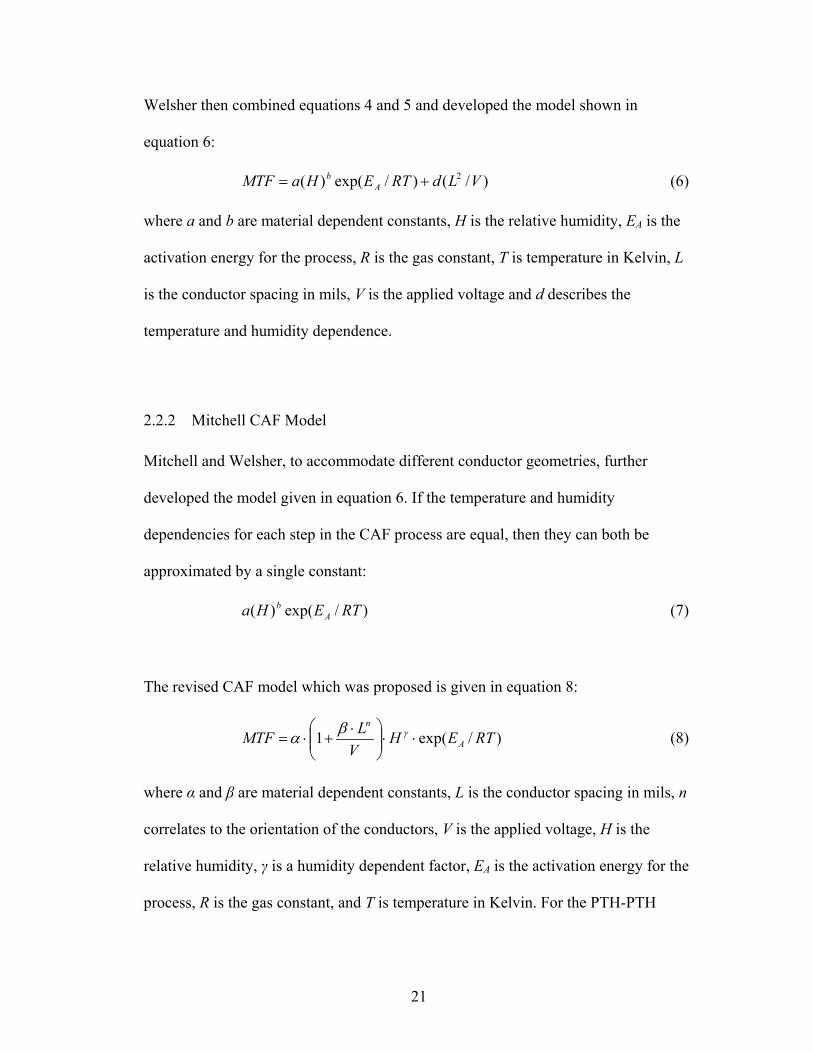
2.2.2 Mitchell CAF Model
Mitchell and Welsher, to accommodate different conductor geometries, further
developed the model given in equation 6. If the temperature and humidity
dependencies for each step in the CAF process are equal, then they can both be
approximated by a single constant:
)/exp()( RTEHa Ab (7)
The revised CAF model which was proposed is given in equation 8:
)/exp(1 RTEHV
LMTF A
n
⋅⋅⎟⎟⎠
⎞⎜⎜⎝
⎛ ⋅+⋅= γβα (8)
where α and β are material dependent constants, L is the conductor spacing in mils, n
correlates to the orientation of the conductors, V is the applied voltage, H is the
relative humidity, γ is a humidity dependent factor, EA is the activation energy for the
process, R is the gas constant, and T is temperature in Kelvin. For the PTH-PTH

22
conductor orientation, n is equal to four. This equation is valid for temperatures
ranging from 50oC to 100oC and a relative humidity range of 60% to 95%.
2.2.3 Augis CAF Model
Augis et al. [8] identified the existence of a moisture threshold for filament formation
and concluded that the linear acceleration factor extrapolations for the high stress
testing used earlier by Bell Labs were not valid. Augis observed that for a 50 V
circuit operating at 25o C, the critical relative humidity necessary to initiate CAF
formation was approximately 80%. A quantitative model to predict this critical
threshold value was developed. This model is given in equation 9.
( ) ( )⎥⎦⎤
⎢⎣⎡ ⋅−++
=47.5
ln52.1/10484ln3975.2exp VTcRH (9)
2.2.4 Rudra CALCE CFF Model
Rudra et al. [9] in conducting research at the CALCE Electronic Packaging and
Research Center used a physics of failure approach to determine that several factors
were involved in determining the time to failure due to conductive filament
formation. These factors were: external operating conditions including temperature,
operating voltage and humidity, laminate parameters including material type, surface
coating (solder mask, solder plate and post coat) and the geometry and spacing of the
conductors. The model that was developed is given in equation 10:
( )( )t
m
neff
f MMVLfa
t−⋅
⋅⋅⋅=
1000 (10)

23
where tf is time to failure in hours, a is the filament formation acceleration factor for
different surface conditions and laminate material, f is the multilayer correction
factor, n is a geometry acceleration factor (determined to be 1.6), V is the applied
voltage, m is a voltage acceleration factor (determined to be 0.9), M is the moisture
content, Mt is the threshold moisture content (determined to be 0.35), and Leff, the
effective length between conductors, is the product of k - the shape factor (ranged
from 0.53 to 1.13) and L - the spacing between the conductors in inches. The
threshold moisture content was calculated using the Augis model for different
voltages and temperatures. Although it may appear that there is no temperature
dependence in the model, the temperature dependence is accounted for in the
calculation of the threshold moisture content (function of temperature and relative
humidity), thus eliminating the necessity for an explicit temperature term.
2.2.5 Li Modified CALCE CFF Model
The CALCE CFF diffusion controlled reaction model proposed by Li et al. [14] for
initiation of the CAF failure mechanism was modified by Sauter [10] to include the
extent of readily conductive region (D) around PTHs based on failure data for FR-4
laminates tested at 100 volts DC bias and 10 volts DC bias. The revised model is
given in equation 11:
( )( ) ( )RTEVHCMFn
DLTRapt f /exp2
2'
2
⋅⎥⎦
⎤⎢⎣
⎡⋅⋅⋅⋅⋅⋅
⋅−⋅⋅⋅⋅= (11)
where tf is time to failure, p is the density of copper, a is the volume fraction of
filament, R is the gas constant, T is temperature in Kelvin, L is the initial electrode

24
spacing, D is the extent of readily conductive region surrounding the PTH, n is the
number of valence electrons (n=2 for Cu++), F is Faraday constant (charge of one
mole of electrons), M is the ion mobility constant (for FR-4), C′ is the copper ion
concentration, H is the relative humidity, V is the applied voltage bias and E is the
activation energy.
2.2.6 Sun Microsystems Model (Based on the CALCE Model)
A model to predict time to failure was developed by Sun Microsystems, based on the
CALCE model. This model, shown in equation 12, accounts for laminate materials,
PTH height (same as board thickness) and the PWB manufacturing process:
( )⎥⎦
⎤⎢⎣
⎡⋅⋅
⋅−⋅⋅=
TVHDLPKt f
2)2( (12)
where tf is time to failure, K is the laminate material constant at standard temperature,
P is the PWB manufacturing process, L is the initial electrode spacing, D is the extent
of readily conductive region surrounding the PTH, H is the relative humidity, a is the
volume fraction of filament, V is the applied voltage bias and T the board thickness.
If parameters likely to be constant for a given laminate and test condition are grouped
together, this equation can be simplified to equation 13:
( )⎥⎦
⎤⎢⎣
⎡ ⋅−∝
VDLt f
2)2( (13)
where the time to failure is proportional to the square of the effective distance divided
by the voltage. The effective distance is L-2D.
25
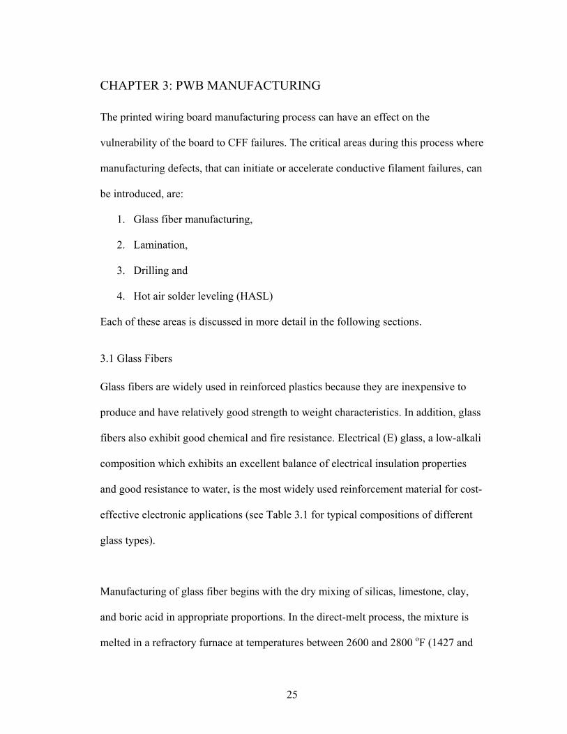
CHAPTER 3: PWB MANUFACTURING
The printed wiring board manufacturing process can have an effect on the
vulnerability of the board to CFF failures. The critical areas during this process where
manufacturing defects, that can initiate or accelerate conductive filament failures, can
be introduced, are:
1. Glass fiber manufacturing,
2. Lamination,
3. Drilling and
4. Hot air solder leveling (HASL)
Each of these areas is discussed in more detail in the following sections.
3.1 Glass Fibers
Glass fibers are widely used in reinforced plastics because they are inexpensive to
produce and have relatively good strength to weight characteristics. In addition, glass
fibers also exhibit good chemical and fire resistance. Electrical (E) glass, a low-alkali
composition which exhibits an excellent balance of electrical insulation properties
and good resistance to water, is the most widely used reinforcement material for cost-
effective electronic applications (see Table 3.1 for typical compositions of different
glass types).
Manufacturing of glass fiber begins with the dry mixing of silicas, limestone, clay,
and boric acid in appropriate proportions. In the direct-melt process, the mixture is
melted in a refractory furnace at temperatures between 2600 and 2800 oF (1427 and

26
1538 oC) and fed directly into bushings, which are platinum alloy trays with
thousands of precisely drilled tubular openings called bushings. Alternatively, the
melt can be formed into marbles, cooled to room temperature and stored for future
use.
A homogeneous melt composition with negligible impurities is necessary for the
successful manufacture of glass fibers. Solid inclusions of even sub-micron
dimensions can act as stress concentrators that reduce the fiber strength. Furthermore,
the decomposition of raw materials during glass melting can lead to trapped gases. In
the raw materials, water, carbonates (CO3), and organic materials will decompose
with heat to form gases. Depending on the viscosity of the glass mixture and various
manufacturing processes, these gases can get trapped as bubbles, called seeds. Seeds
are a naturally occurring part of the process and thus methods to remove them are
necessary. One approach is fining. Fining removes gases by adding gases (i.e., SO2),
which create nucleation sites for bubbles to coalesce and escape the melt. Fining can
also be defined as increasing the temperature and modifying the heat flow pattern so
bubbles are moved in positions to readily reach the surface and escape.

27
Table 3.1. Typical Chemical Weight % Composition of Major Components in Fiberglass [Watt and Perov, 1985]
Composition E-Glass A-Glass C-Glass S-Glass SiO2 54.8 72.0 65.0 65.0 Al2O3 11.5 0.6 4.0 25.0 B2O3 5.5 - 5.5 0.01 CaO 18.0 10.0 14.0 0.01 MgO 5.0 2.5 3.0 10.2 K2O 0.8 14.2 8.5 BaO - - - 0.2
Fe2O3 0.1 - - 0.2
After the molten glass is poured into the bushing, glass fibers are produced by
drawing a solidified filament of glass from a molten drop. The diameter of a glass
fiber is typically between 5 and 25 microns. During drawing, any seeds present will
become attenuated and elongated, forming capillaries several meters long in the glass
filaments and effectively creating hollow fibers [Morley 1987]. These hollow fibers
can provide a path for conductive filament formation.
3.2 Production of Fiber Weaves
Individual fibers being drawn from the nozzles in the bushing pass through a light
water spray and then over an applicator that transfers a protective and lubricating size
onto the filaments. Glass fibers are then gathered together to form a strand and wound
on a rotating cylinder called a “collet”. When winding glass fibers on collets at high
velocity, breakage of the fibers can take place due to the mutual friction of the fibers
as well as friction against directing parts. Fiber sizes, also known as coatings, are
applied to the surface of fibers to prevent loss of strength and damage to the fibers
28
during the manufacturing process. Lubricants, fed in the region of formation, can
minimize this breakage. Besides solvents, these lubricants contain sticking
substances, plasticizers and emulsifiers. Distilled water is commonly used as a
solvent, whereas latex, paraffin, starch and gelatin are used for fibers sticking and
vegetable and mineral oils as plasticizers. Coupling agents may also be applied when
the fibers are going to be embedded in a polymeric matrix, to improve bonding
between the fibers and the matrix. Bonding is important if the composite material is
required to perform under various temperature and humidity conditions. It has been
found that hydroxyls present on the surface of glass fibers can increase moisture
affinity to the glass.
The term strand refers to a unidirectional bundle of fibers (102, 204 or 408
fibers/bundle) drawn from a single bushing. The strands are then twisted into yarns.
In the electronic substrate industry, the yarns are typically woven into a plain weave
fabric, which is impregnated with an epoxy to form a laminate.
3.3 Lamination
During the lamination process the thin-core inner-layers are subjected to heat and
pressure and compressed into a laminated panel. Sheets of material consisting of glass
fibers impregnated with epoxy resin, known as pre-preg or b-stage, are slipped
between the layers and bond the layers together. Pre-preg is available in different
styles with varying ratios of resin to glass fibers. This choice of differing epoxy resin
to fiber glass ratios allows the manufacturer to control the thickness between layers

29
and to provide the appropriate amount of resin flow between circuitry. Lamination
steps are fairly consistent among manufacturers. All of the materials, including the
inner-layers and pre-preg, are tooled to the same registration system and held in place
by tooling pins. Several panels can be pressed together in one set of heavy plates,
creating what is known as a "book”. In lamination, the pressing parameters must
closely match what the laminator recommends. If the heat rise of the pressed book is
too fast or too slow, the resin will not have enough time to properly wet-out the cores
that are being pressed. Laminate voids or other lamination defects may occur,
allowing paths for CFF failures.
3.4 Hole Drilling
Holes are drilled through the PWB to interconnect circuitry on different layers and to
also allow for the insertion of components. The etched innerlayer pattern will extend
to the barrel of the hole and therefore will be interconnected with the other layers
when the hole barrel is made conductive in a later step. Most drilling is performed
with computer numerical control (CNC) equipment, but as hole sizes less than 0.012
inches have become more common, other methods of making small holes are
increasing in popularity. Two alternate methods are punching and laser processing.
The drilled hole should be smooth and straight. There should not be any exposed
glass fibers in the hole, no extreme gouging, and no fracturing of the resin in the hole.
As the boards are processed through the electroless and plating chemistries, the hole
wall may be further degraded, and moisture may be allowed to wick into the board.
This may also contribute to CFF failures.

30
3.5 Surface Finishes
For most parts, the functions of the surface finish are to prevent copper oxidation,
facilitate solderability, and prevent defects during the assembly process. A number of
metallic alternatives exist along with organic solderability preservatives (also known
as OSPs or pre-fluxes). A variety of deposition techniques exist, including hot air
leveling, electroplating, immersion, and electroless plating. The shelf life of
immersion, electroless plated, and OSP coating alternatives are less than that of
leveled or tin-lead reflowed boards. Other surface finishes are dictated by the
environment in which the part will reside or by specific performance criteria.
Solder-mask-over-bare-copper (SMOBC) with hot-air-solder-leveling (HASL) has
been the preferred surface finish for over 15 years. Nickel-gold, another popular
finish, can be applied electrolytically as an etch resist, replacing tin and tin-lead, or
electrolessly as a substitute for HASL. Other electrolytic plating metals include
rhodium, palladium, palladium-nickel alloys, and ruthenium. Non-electrolytic
deposition processes include tin immersion, tin-lead displacement plating, electroless
nickel, electroless gold, immersion gold, immersion silver, immersion bismuth, and
the previously mentioned OSPs. The purpose of solder mask is to physically and
electrically insulate those portions of the circuit to which no solder or soldering is
required. Increasing density and surface mount technology have increased the need
for solder mask to the point that, with the exception of "pads only" designs, nearly all
parts require it. Manufacturers have had some autonomy in selecting masks. Many
specifications do not call out a specific product or product type, allowing the
manufacturer to choose masks based on processing as well as performance issues.

31
Three basic types of masks are commonly applied: thermally cured screen-printed
masks, dry film, and liquid photoimageable (LPI). Thermal masks have predominated
for decades but are gradually being replaced by LPI, despite being the lowest cost
alternative. Dry film has some specific advantages, such as ease of application, but its
use seems poised to decline as well in the face of improving LPI formulations.
The HASL process consists of a pre-clean, fluxing, hot air leveling, and a post-clean.
Pre-cleaning is usually done with a micro-etch. However, the usual persulfate or
peroxide micro-etch is not common in the process. Dilute ferric chloride or a
hydrochloric-based chemistry is favored for compatibility with the fluxes that are
applied in the next step.
Fluxes provide oxidation protection to the pre-cleaned surface and affect heat transfer
during solder immersion. The fluxes also provide protection against oxidation during
HASL (hot air solder level). Higher viscosity fluxes provide better oxidation
protection and more uniform solder leveling, but reduce overall heat transfer and
require a longer dwell time or higher temperature. A balance in flux use must be
struck between better protection with high viscosity fluxes and superior heat transfer
with lower viscosity fluxes.
All areas of exposed copper are coated with solder while masked areas remain solder-
free. Boards are then cleaned in hot water, the only step in the SMOBC process where
lead may enter the wastewater stream, in very small quantities. Once cleaned, the

32
panels may again enter the screening area for optional nomenclature screening, or
proceed directly to the routing process.
Copper, flux, and other impurities increase in concentration in the solder pot as panels
are continuously processed through the hot air leveler. These impurities can be
removed to some degree by performing a procedure known as drossing. The
impurities will float to the surface of the solder where they can be scooped out and
placed in a dross bucket. This material can be returned to the vendor for reclamation
of the metals. Some manufacturers go for years without changing the solder; they
dross and make additions. When the time comes to change over the solder, vendors
will issue credit on the purchase of new solder as long as the old solder is returned to
them for processing. HASL temperatures and certain fluxes can also contribute to
CFF failures. The high, temperatures may exceed the Tg of the material, and
depending on the type of coating used, moisture uptake may be enhanced. Any
residue left on the board may also be an issue.

33
3.6 Defects that may Initiate and Accelerate CFF Failures
During failure analysis conducted on defective PWBs, some of the manufacturing
defects that can initiate and accelerate CFF failures were observed. Following the list
of defects, are photos and descriptions representative of most:
• Fiber/resin separation (see Figure 4)
• Conductor/resin separation (see Figure 5)
• PTH/resin separation (see Figure 6)
• Degradation of conformal coating layer
• Mis-registration (see Figure 7)
• Copper wicking (see Figure 8)
• Drilling damage (see Figure 9)
• PTH plating cracks (see Figure 10)
• Hollow fibers (see Figure 11)

34
Figure 4. Fiber/resin interface delamination can occur as a result of stresses generated under thermal cycling due to a large CTE mismatch between the glass fiber and the epoxy resin (approximately 5.5 ppm/oC and 65 ppm/oC respectively) and poor bonding at the fiber/resin interface. Delamination can be prevented/resisted by selecting resin with lower CTE’s and optimizing the glass surface finish. Studies have shown that the bond between fiber and resin is strongly dependent upon the fiber finish.
Figure 5. Moisture can condense in the copper/resin separated areas, allowing the copper to ionize, and migrate towards adjacent conductors.

35
Figure 6. A separation can be seen at the copper plating to fiber epoxy resin board interface. These gaps provide areas for moisture to condense and CFF to initiate. These voids which can be adjacent to inner-layer copper foils or PTH barrels, normally result from contraction of the epoxy (resin recession).
Figure 7. This optical image shows misregistration between a solder filled PTH and a power plane. Misregistration can decrease conductor spacing, effectively increasing the PWB’s electric field strength in the closer conductor spacings.

36
Figure 8. Copper wicking can be serious if it extends sufficiently to increase the electric field strength or decrease the internal resistance breakdown between PTHs. Furthermore, it provides a convenient starting point for CFF as it effectively decreases the conductor spacing.
Figure 9. The anomalies seen around the PTH, known as micro-cracking, are primarily caused by excessive heat or mechanical loads due to non-optimized drilling parameters. Drilling has become a very complex process with regard to the selection of optimum drill parameters for high performance materials. New drill bit compositions and geometries are most important among these factors.

37
Figure 10. Since the difference in the coefficient of thermal expansion (CTE) of the copper plating and the resin system in the PWBs is at least a factor of 13, stress exerted on the plated copper in the plated-through holes in the z-axis during thermal excursions can cause cracking. These cracks provide areas for moisture to condense and for CFF to initiate.
Figure 11: Hollow fibers are vacuous glass filaments in E-glass laminates which can provide paths for CFF. Generally CFF is a two-step process, dependent upon temperature-cycling or high temperature/humidity induced debonding between the glass fibers and epoxy resin matrix in providing a path for copper migration. With the appearance of hollow fibers inside the laminates, CFF can happen as a one step process.

38
3.7 Summary
This chapter provided a thorough review of the defects that may be introduced into a
printed circuit board during the manufacturing process steps. While the presence of
these defects is crucial to understanding the occurrence of certain filament driven
failure phenomenon, classical theory states that the formation of a path in which the
filament grows is the rate limiting step for this mechanism. These paths may be
preexisting in the laminate because of the existence of hollow fibers or may develop
as a function of applied external stresses on other defects. This dissertation provides
the methodologies, specific for electronic products, for detecting hollow fibers and
locating CFF related failures. The dissertation also provides experimental and
analytical investigations of path formation in glass epoxy composites.
39
CHAPTER 4: HOLLOW FIBER DETECTION
4.1 Introduction
R.J.B. Hadden and A. Kirk, using a technique developed by the Fermi National
Accelerator Laboratory, originally proved the existence of hollow fibers in glass
fabrics. This technique has been modified to optimize the hollow fiber assessments.
The following sections describe this process in detail. Hollow fiber assessment
experiments show how hollow fiber densities can vary between different
manufacturers and also within the same manufacturer based on the laminate type (e.g.
high Tg versus low Tg). Some of the resin types assessed were polyimide (PI),
bismaleimide triazine (BT), cyanate ester (CE), flame retardant (FR-4), a high-
temperature FR-4, and Driclad, an IBM high Tg laminate advertised as having low
moisture uptake.
4.2 Measurement Techniques for Hollow Fibers in Common Laminates
Laminates are cut along the diagonal into 10 x 10 cm test coupons to allow for ease of
handling, sample preparation, and observation through an optical microscope (see
Figure 12). Since the hollow fibers usually traverse the entire length of the laminate,
cutting samples along the diagonal insures that each hollow fiber is accounted for
only once. If the laminates are copper cladded, the copper can be removed by
submerging the copper cladded laminates in aqua regia, a chemical solution of
concentrated hydrochloric and nitric acid, for about 10 to 15 minutes. This is

40
performed in a fume hood, using the appropriate protection as necessary for working
with hazardous chemicals (see Figure 13).
Figure 12. This photo shows the diagonal sections (black dot in middle) that are used for the hollow fiber assessments. By using only the sections on the diagonal, ensues that each hollow fiber is not accounted for more than once.
Figure 13. Placing the copper cladded laminates in a chemical solution of concentrated hydrochloric and nitric acid (aqua regia), for about 10 to 15 minutes, effectively removes all exposed copper from the surfaces. This is done in a fume hood, using the appropriate protection necessary for working with hazardous chemicals.

41
Samples are then placed in an oven at 538 oC (1000 oF) for approximately 60 to 90
minutes (depending on the resin type and laminate thickness) to burn off the resin and
expose the bare glass bundle matrix (see Figure 14). The initial burn-off temperature
of 600 oC, as suggested by industry, was found to result in the fracture of glass fibers
during handling as they became brittle. By trial and error, a burn-off temperature of
538 oC was selected. This optimized the burn-off time while still maintaining the
integrity of the glass fabric. After separating the individual fabric layers, each of the
four sides for each individual fiber glass fabric layers was subsequently sealed with
wax to prevent wicking, the capillary action of a fluid into a hollow fiber.
Figure 14. Photo showing before and after resin removal The technique used by the Fermi National Accelerator Laboratory to investigate leaks
in fiberglass-reinforced pressure vessels was employed to observe hollow glass fibers.
Each fabric layer is submerged in oil with an optical refractive index that can be
either similar to or slightly different (± 0.002) than that of the glass fibers and allowed
to sit overnight (this allows the oil to completely saturate the fiber mat). Light is then
directed onto the coupon, now saturated with the refracting oil. The light travels
42
freely until it hits a hollow fiber, where the change in refractive index at the fiber-air
boundary partially reflects it. The unreflected light continues to propagate until it hits
the outgoing air-fiber boundary, where again it is partially reflected (see Figure 15).
Using a black background can improve the visibility of the hollow fibers. The hollow
fiber detection setup is shown in Figure 16. Even though hollow fibers are visible to
the naked eye, a low magnification microscope attachment is best to view them (see
Figure 17). While each of the methods (oil with an optical refractive index that can be
either similar to or slightly different than that of the glass fibers) provides a means to
optically view the hollow fibers, using an oil with the same refractive index as the
glass fibers allows only the hollow fibers to be seen, whereas, using an oil with a
slightly different refractive allows not only the hollow fibers to be seen, but also
faintly shows the glass fabric weave. This method can produce an image of the glass
fiber fabric and the hollow fibers simultaneously. Both oils, with the equal refractive
index, (see Figure 18) and with the slightly different refractive index (see Figure 19)
are shown. The oil with the slightly different refractive index is preferred, since both
the hollow fibers along with the fabric weave can be viewed simultaneously. The
refractive index of E-glass is 1.550, while that of the oil (Tricresyl Phosphate) is
1.553, giving a difference of 0.003.
In one experiment, the number of hollow fibers observed in several 2 x 2 inch
coupons ranged from 0 to 158. Six to eight samples were tested for each laminate
type. The IBM Driclad laminate, promoted as “hollow-free fabric” to prevent
conductive filament formation (CFF), had an average of 16 hollow fibers/1,000 in2.

43
Figure 15. Light travels freely until it hits a hollow fiber. The change in the refractive index at the fiber/air boundary partially reflects the light.
Figure 16. A change in the refractive properties is evident through an optical microscope by a bright white line. In some cases, a hollow fiber could be detected without using a microscope. The light source is positioned so that light enters the edge of the fabric perpendicular to the fibers being observed.

44
Figure 17. Although hollow fibers are visible to the naked eye (see arrows), a microscope attachment is best to view them.
Figure 18. The edges of this sample were not dipped in wax. As the sample was submerged in oil, the oil started to flow into one of the hollow fibers. A mark was set at one point of the hollow fiber so that the movement of the oil could be more easily visualized. Only the hollow fiber is visible, due to the exact match between the refractive index of the oil and the fiber glass.

45
Figure 19. Hollow fibers can be seen as white lines traveling along the fiber bundle weave in these pictures. The refractive index of E-glass is 1.550, while that of the oil used here is 1.553. This difference of 0.003, allows the fabric weave to also be seen.
4.3 Discussion of the Hollow Glass Fiber Problem
Multi-layer organic laminates used in printed wiring boards and laminated multichip
modules (MCM-L) can develop a loss of insulation resistance between two biased
conductors due to the growth of conductive filaments. The phenomenon, called
conductive filament formation (CFF) or electromigration, is an electrochemical
process which involves the transport, usually ionically, of a metal through or across a
nonmetallic medium under the influence of an applied electric field. The growth of
metallic filaments is a function of temperature, humidity, voltage, laminate materials,
manufacturing processes, and the geometry and spacing of the conductors.
CFF is most prone to occur between biased conductor such as vias and plated-through
holes (PTHs), but can also occur between two traces (usually copper) or between a
trace and a via or PTH [Rudra and Pecht 1994]. The formation of a continuous

46
metallic path through or on the outside of the fiber can result in an electrical short.
Hollow fibers are vacuous glass filaments in E-glass laminates which can provide
paths for conductive filament formation (CFF). Generally, CFF is a two-step process,
dependent upon temperature-cycling and/or humidity-cycling induced debonding
between the glass fibers and epoxy resin matrix to provide a path for copper
migration. With the appearance of hollow fibers inside the laminates, CFF can happen
as a one step process. A photo of a partially copper-filled hollow fiber bridging and
electrically shorting two adjacent PTHs in a PWB is shown in Figure 20. CFF is
nearly impossible to detect in the field because once it occurs, sufficient heat is
generated to “vaporize” the conductive filament and “clear” the failure. Furthermore,
observation of a partial filament formation requires destructive analysis. It is nearly
impossible to screen a circuit card in order to precipitate CFF, in part because of the
ability of the problem to heal itself.
Figure 20. Hollow fibers are vacuous glass filaments in E-glass laminates which can provide paths for conductive filament formation (CFF). Generally CFF is a two-step process, dependent upon temperature-cycling and humidity-cycling induced debonding between the glass fibers and epoxy resin matrix to provide a path for copper migration. With the appearance of hollow fibers inside the laminates, CFF can happen as a one step process.
47
4.4 Failure Opportunities due to Hollow Fibers
Research has shown that PTH-to-PTH CFF failures represent the most significant
population of failure opportunities, especially compared with line-to-line or line-to-
PTH metallization failures [9, 10]. Thus, PTH-to-PTH adjacency is a suitable
measure of hollow fiber failure opportunity. CFF failure opportunity is proportional
to the probability of a hollow fiber connecting two adjacent plated-through-holes
(PTHs). This probability is proportional to the density of PTHs in the circuit card, the
number of fibers that the PTHs are in intimate contact with (PTH diameter vs. grid
spacing, see Figure 21), and the hollow fiber density of the circuit card.
The PTH density depends on the circuit card layout design rules and the allowable
exceptions. The number of fibers that each PTH is in intimate contact with depends
on PTH diameter, fabric style (number of bundles/square inch, number of individual
fibers/bundle), and the thickness of the board (number of laminate layers and
individual glass fabric mats). An E-SEM photo of a cross-sectioned area in a woven
laminated printed circuit board containing two PTHs is shown in Figure 22.
To make the calculations easier to follow, assume that each PTH runs through the
entire thickness of the board (i.e., no blind or buried PTHs are considered) and that
each PTH has the same diameter. To accommodate for blind or buried PTHs, or PTHs
of differing diameters, changes in the total number of filaments that are in contact
with PTHs can be adjusted based on changes in PTH dimensions.
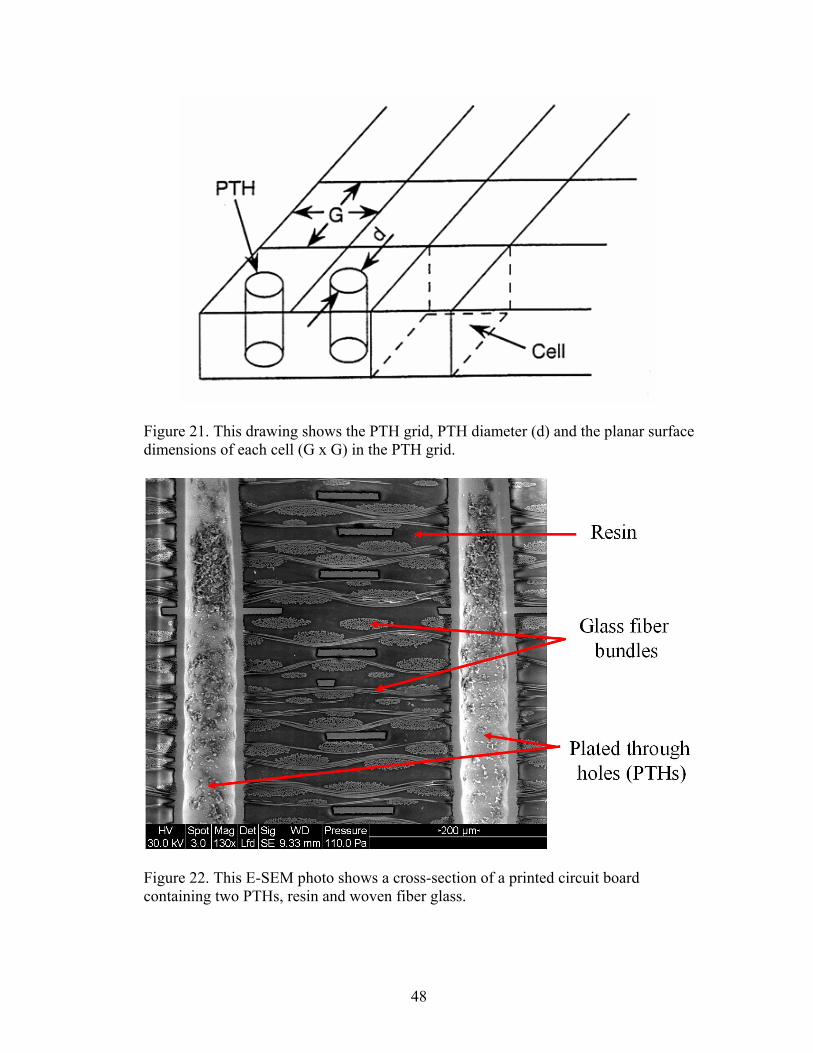
48
Figure 21. This drawing shows the PTH grid, PTH diameter (d) and the planar surface dimensions of each cell (G x G) in the PTH grid.
Figure 22. This E-SEM photo shows a cross-section of a printed circuit board containing two PTHs, resin and woven fiber glass.
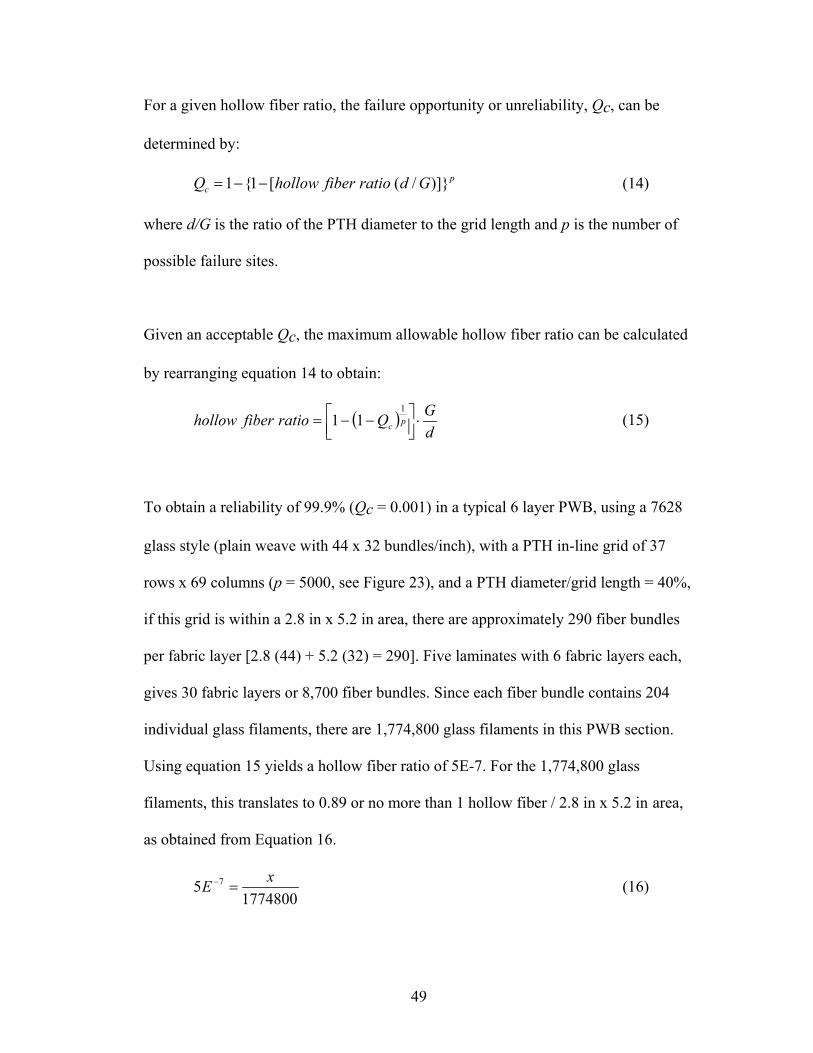
49
For a given hollow fiber ratio, the failure opportunity or unreliability, Qc, can be
determined by:
pc GdratiofiberhollowQ )]}/([1{1 −−= (14)
where d/G is the ratio of the PTH diameter to the grid length and p is the number of
possible failure sites.
Given an acceptable Qc, the maximum allowable hollow fiber ratio can be calculated
by rearranging equation 14 to obtain:
( )dGQratiofiberhollow pc ⋅⎥⎦
⎤⎢⎣⎡ −−=
111 (15)
To obtain a reliability of 99.9% (Qc = 0.001) in a typical 6 layer PWB, using a 7628
glass style (plain weave with 44 x 32 bundles/inch), with a PTH in-line grid of 37
rows x 69 columns (p = 5000, see Figure 23), and a PTH diameter/grid length = 40%,
if this grid is within a 2.8 in x 5.2 in area, there are approximately 290 fiber bundles
per fabric layer [2.8 (44) + 5.2 (32) = 290]. Five laminates with 6 fabric layers each,
gives 30 fabric layers or 8,700 fiber bundles. Since each fiber bundle contains 204
individual glass filaments, there are 1,774,800 glass filaments in this PWB section.
Using equation 15 yields a hollow fiber ratio of 5E-7. For the 1,774,800 glass
filaments, this translates to 0.89 or no more than 1 hollow fiber / 2.8 in x 5.2 in area,
as obtained from Equation 16.
17748005 7 xE =− (16)

50
Solving for x gives 0.89. Therefore, in a typical board with these specifications, there
must be less than 1 hollow fiber per 2.8 in x 5.2 in area in the board, to have a failure
opportunity less than 0.001, due to filament formation between adjacent PTHs
through a hollow fiber. These calculations assume that conditions are conducive for
CFF. For different conductor geometries or PWB thickness, the allowable hollow
fiber ratio, based on an acceptable reliability, can be recalculated.
On the Fujitsu M-780 large-scale general purpose computer, there are more than
80,000 PTHs per circuit card. A section of a PWB containing over 6,000 PTHs is
shown in Figure 24.
Figure 23. For a 37 x 69 grid of PTHs, where x = 37 PTH rows and y = 69 columns in the grid, the number of possible adjacent PTH failure sites can be calculated by: (37+68)(69+36) = 5,000 possible failure sites. In a square grid, where x = y, this simplifies to 2[x(x-1)] or ~2x2 for x > 100.

51
Figure 24. This PWB section (half of board used by AVICI Systems) contains close to 7,000 PTHs. On the Fujitsu M-780 large-scale general purpose computer, there are more than 80,000 PTHs per circuit card.

52
CHAPTER 5: ANALYZING CAF FAILURES
There are basically three methods for detecting and locating CAF failures; electrical
testing, thermal imaging and superconducting quantum interference device (SQUID).
Each technique is unique, and in some situations may be the only available choice to
verify that a failure exists and locate the failure site. After the failure is verified and
the site identified, cross-sectional techniques can be employed to allow microscopic
examinations and elemental analysis of the defective area.
5.1 Electrical Testing
In cases where the shorted conductors can be traced via circuit schematics, and no
ground or power planes are involved in the shorted site, electrical probing may be a
viable technique for locating the defective site via resistance checking (see Figure
25). In this technique, the approximate resistance values between conductors based on
the circuit design should be available to verify locations where low resistance values
can be attributed to defects and not to design. It is important to isolate the suspected
shorted conductors from the rest of the circuit, and verify that no superficial anomaly
such as surface contamination or debris is contributing to the low resistance value
observed (i.e., the shorted site is internal). For complex circuitry where it is not
possible to isolate the suspected conductors, electrical testing may be of lesser value.
After verification of the failure, subsequent cross-sectional techniques, while
continuously monitoring the resistance of the shorted conductors, may resolve the
precise failure site and uncover defects that may have initiated or accelerated the
failure, by optical and E-SEM inspections.

53
Figure 25. Conductor geometry of shorted adjacent PTHs where electrical testing may be used to verify the existence of an internal short in a PWB, after isolation from the rest of the circuitry (removal of the surface traces) is shown.
5.2 Thermal Imaging
Thermal imaging is technique that has been successfully used to locate shorted
locations by monitoring the changes in temperature as a defective board is powered.
When power is applied to the defective board, a higher than normal current flows
through the shorted conductors, and can cause a localized temperature rise in the
affected area. A suitable level of current, which is high enough to cause a rise in
temperature at the localized shorted site, while at the same time not destroying or
“blowing” the fragile fuse-like filament, must be obtainable. If this suitable level of
current can be obtained, and the equipment is sensitive enough to detect minute
temperature rises, this technique can overcome disadvantages such as complex
circuitry and shorts involving conductor planes, which limit electrical testing.
However, due to the nature of the conductive filaments, many of them are fragile, and
the current necessary to cause a detectable temperature rise in the shorted site can
destroy them. One successful analysis using thermal imaging to verify and locate a
short involving a ground plane can be seen in Figure 26 where the hot spot is

54
identified, and the short between the PTH and ground plane found by subsequent
cross-sectional techniques (see Figure 27).
Figure 26. The photo at the top shows the thermal imaging equipment, while the photo at the bottom shows a sequential series of snapshots (clockwise starting at top left) as the power is turned on, identifying the shorted area.
Figure 27. After locating the defective area by thermal imaging, subsequent cross-sectional techniques verified that there was an internal short between a PTH and ground plane.

55
5.3 Superconducting Quantum Interference Device
Superconducting quantum interferance device (SQUID) microscopy is a new
technique that uses detection of magnetic fields to image current paths within
electronic devices (see Figure 28). This technique has been successful in non-
destructively identifying the location of low leakage currents, even when the failure
site was between a power and ground plane (roughly equivalent to finding a needle in
a haystack). The use of low voltage and low current can be superior to thermal
imaging. Thermal imaging can result in irreplaceable damage to the failure site and
masking of the true root cause of failure when a high amount of current is required to
generate sufficient heat to be detectable. A photo of the current mapping output from
the SQUID is shown in Figure 29. The shorted site, bridging two copper planes, was
located after cross-sectioning, based on the SQUID results (see Figure 29 and Figure
30.
Figure 28. Photo of the superconducting quantum interference device equipment

56
Figure 29. SQUID current mapping technique used to locate short circuit between planes in a PWB
Figure 30. An optical image shows the shorted site located between two planes, after cross-sectioning based on the SQUID results.

57
Although the SQUID has unique advantages, it also has limitations. In addition to
being costly, the SQUID it is limited to ~ 100 µm maximum working distance above
the shorted site. Due to this, the SQUID may not be applicable to populated areas on a
PWB where the height of components or connectors over the failed location can
interfere with the working distance restrictions. For example, the SQUID could not
have been used in the previous thermal analysis, due to the height of the connectors
on the board.
Since the test boards in this dissertation are unpopulated, and the conductive
filaments formed are fragile, the SQUID was used in verifying and locating the
shorted sites.

58
CHAPTER 6: CFF EXPERIMENTS
Accelerated tests to characterize conductive filament formation failure behavior in
laminated printed wiring boards subjected to high temperature and high humidity
environments were conducted, using four laminate types, three conductor spacings
and voltages ranging from 1 volt to 100 volts DC.
6.1 Test Board Design
Based on a literature review of the current test methods (IPC-TM-650 2.6.25,
Telcordia GR-78 and Sun Micro Systems) and test board designs, parameters for the
test coupons were selected. The design of the test boards used in this study is shown
in Figure 31.
Figure 31. Design of the CFF test board used in this study The IPC-TM-650 test board has 840 in-line PTH-PTH and 744 staggered PTH-PTH,
the previous CFF testing conducted by Rudra et al. [1994] had 412 in-line PTH-PTH
in the test board, and a board used by NPL [2004], contained over 6,000 PTHs. The
PTH-PTH spacings previously used were, 11-25 mils edge-to-edge (IPC-TM-650), 5-

59
65 mils (Rudra, 1994) and 12-32 mils edge-to-edge (NPL, 2004), while the PTH-
internal plane (aka anti-pad) spacings were 10-24 mils (IPC-TM-650), 10-20 mils
(Rudra, 1994) and 16 mils: PTH wall – plane and 6-10 mils PTH pads – plane (NPL,
2004).
For this study, the test board design contains 600 in-line PTH-PTH and 100 PTH-
plane conductors, with PTH-PTH spacings and PTH-internal plane spacings based on
current technology and manufacturing limitations (see Figure 32). The three different
feature sizes in both conductor geometries (PTH-PTH and PTH-plane) were selected
to be representative of nominal, advanced and next generation feature sizes in
electronics. The nomenclature of the three designs and conductor feature sizes were:
• Nominal (NF): PTH-to-PTH = 6 mil, PTH-plane = 8 ± 1 mil,
• Advanced (AF): PTH-to-PTH = 4 mil, PTH-plane = 6 ± 1 mil, and
• Next generation (XG): PTH-to-PTH = 3 mil, PTH-plane = 3 ± 1 mil
A B Figure 32. The photos in A and B give examples of the PTH-PTH and PTH-plane conductor geometry features respectively.
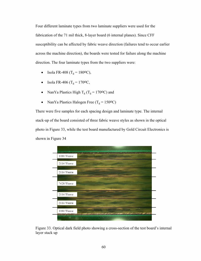
60
Four different laminate types from two laminate suppliers were used for the
fabrication of the 71 mil thick, 8-layer board (6 internal planes). Since CFF
susceptibility can be affected by fabric weave direction (failures tend to occur earlier
across the machine direction), the boards were tested for failure along the machine
direction. The four laminate types from the two suppliers were:
• Isola FR-408 (Tg = 180oC),
• Isola FR-406 (Tg = 170oC,
• NanYa Plastics High Tg (Tg = 170oC) and
• NanYa Plastics Halogen Free (Tg = 150oC)
There were five samples for each spacing design and laminate type. The internal
stack-up of the board consisted of three fabric weave styles as shown in the optical
photo in Figure 33, while the test board manufactured by Gold Circuit Electronics is
shown in Figure 34
Figure 33. Optical dark field photo showing a cross-section of the test board’s internal layer stack up

61
Figure 34. Photo shows the test board with the PTH-PTH grid (left) and the PTH-internal plane (right) test patterns.
6.2 Test Procedure
The boards were tested in accordance with IPC-TM-650 2.6.25, Conductive Anodic
Filament (CAF) Resistance Test: X-Y Axis [18]. Each board was uniquely identified
with a permanent marker, making marks away from the biased areas of the
specimens. The test boards were handled by the edges only, using non-contaminating
gloves. Each of the two circuits in each test board was prescreened for short circuits
by performing an as-received insulation resistance measurement check. To dry out the
samples, the selected boards were baked for six hours at 105oC prior to each test. For
the preconditioning, the samples, after baking were allowed to sit in a bias free state
for 24 hours at 23oC and 50% RH. The insulation resistances were again measured
prior to a 96-hour stabilization period with no applied bias, at 85oC/85% RH. After
this stabilization period, the selected bias was applied and insulation resistance
measurements were started. All insulation resistance readings prior to the biased test
were made with a FLUKE 189 True-rms Digital Multimeter (resistance range of 0 to
500 Mega-ohms). Prior to all tests, the measured insulation resistance of both test

62
circuits in each board was greater than 500 Mega-ohms. In the chamber, the boards
were setup so that the air-flow was parallel to the direction of the test boards. The
boards were also spaced approximately 2 inched apart (see Figure 35).
Figure 35. Photo of the boards hanging in the environmental chamber, parallel to the air flow and spaced approximately 2 inches apart. The temperature and humidity of the chamber were monitored and plotted so that
deviations from the set conditions could be observed (see Figure 36).
6.3 Insulation Resistance Monitoring Equipment
To monitor the insulation resistance of the boards as they were subjected to the
humidity/temperature/bias testing, an Agilent 4349B High Resistance Meter was used
in conjunction with power supplies, an interface box, an Agilent E5250A Multiplexer,
a universal serial bus (USB) connected to a general-purpose interface bus (GPIB) and
then to a computer. A schematic block diagram of the setup is shown in Figure 37

63
Figure 36. Monitoring and plotting system used to check variations in temperature and humidity settings
Figure 37. Block diagram of equipment setup to monitor insulation resistance

64
The different cable types and twisted wire pairs were used to minimize interference
and noise. The system can accept 3 different voltage inputs and monitors 48 channels.
Figure 38. Schematic of the electrical circuitry used for monitoring the insulation resistance
A schematic of the electrical monitoring circuitry is shown in Figure 38 while the
normal current path, and the current path during device monitoring are shown in
Figure 39 and Figure 40 respectively.

65
Figure 39. The normal current path is shown in red, going through a shorting box.
Figure 40. The current path, shown in red, obtained by “opening” the shorting box, and allowing the current to flow through the electrometer,was used when a device was being tested.
66
The specifications of interest for the Agilent 4349B High Resistance Meter are:
Measurement time (10 –40 ms),
Resistance (103 – 1015) ohms
Delay time (0 – 10 seconds in steps of 0.001 seconds)
Current (1 picoamp – 100 microamps)
As shown in the schematic of the electrical monitoring circuit, a 1-megaohm current
limiting resistor was placed in series with the current path to prevent “blow-out” of
the fragile filaments when shorting occurs. For the each test, 20 boards (5 of each
type) were used since the system could monitor only 48 channels, and each board had
two circuits. Each of the boards had to be electrically connected to the interface box,
which was then connected to the power supplies and the multiplexer unit (see Figure
41). Each of the electrical connections between the boards and the interface box was
uniquely labeled to identify the sample and the monitoring channel for each of the
respective samples.

67
Figure 41. Light colored wires were used for the positive connections (yellow and white) while the darker colored wires (purple and blue) were used for the negative connections. This nomenclature helped to avoid polarity mix-ups.
6.4 Moisture Absorption Characterization
One sample from each of the four laminate types was examined for moisture
absorption characteristics. This was accomplished by first drying each of the samples
at 105oC until there was a negligible decrease in weight, indicating that virtually all of
the moisture had been driven off. The balance used to determine the weight change
was a Mettler AE 100, accurate to 0.0001 grams. The weight percent increase due to
absorbed moisture in an environment of 85oC/85% RH was calculated by:
%100% ⋅⎟⎟⎠
⎞⎜⎜⎝
⎛ −=
o
oi
WWWAbsorptionMoisture (17)
where, Wi is the new weight after exposure at certain intervals, and Wo is the dry
weight.
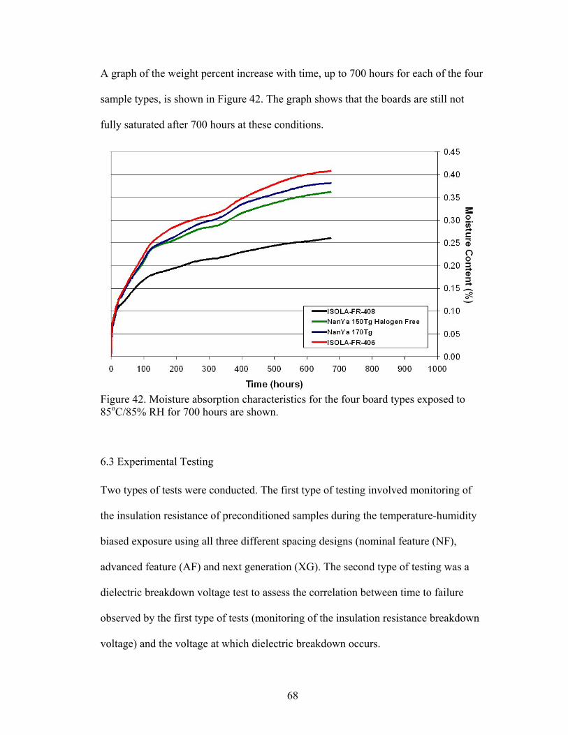
68
A graph of the weight percent increase with time, up to 700 hours for each of the four
sample types, is shown in Figure 42. The graph shows that the boards are still not
fully saturated after 700 hours at these conditions.
Figure 42. Moisture absorption characteristics for the four board types exposed to 85oC/85% RH for 700 hours are shown.
6.3 Experimental Testing
Two types of tests were conducted. The first type of testing involved monitoring of
the insulation resistance of preconditioned samples during the temperature-humidity
biased exposure using all three different spacing designs (nominal feature (NF),
advanced feature (AF) and next generation (XG). The second type of testing was a
dielectric breakdown voltage test to assess the correlation between time to failure
observed by the first type of tests (monitoring of the insulation resistance breakdown
voltage) and the voltage at which dielectric breakdown occurs.
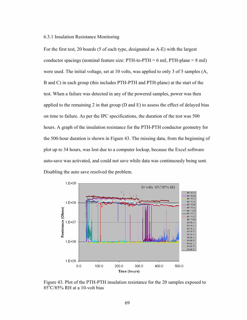
69
6.3.1 Insulation Resistance Monitoring
For the first test, 20 boards (5 of each type, designated as A-E) with the largest
conductor spacings (nominal feature size: PTH-to-PTH = 6 mil, PTH-plane = 8 mil)
were used. The initial voltage, set at 10 volts, was applied to only 3 of 5 samples (A,
B and C) in each group (this includes PTH-PTH and PTH-plane) at the start of the
test. When a failure was detected in any of the powered samples, power was then
applied to the remaining 2 in that group (D and E) to assess the effect of delayed bias
on time to failure. As per the IPC specifications, the duration of the test was 500
hours. A graph of the insulation resistance for the PTH-PTH conductor geometry for
the 500-hour duration is shown in Figure 43. The missing data, from the beginning of
plot up to 34 hours, was lost due to a computer lockup, because the Excel software
auto-save was activated, and could not save while data was continuously being sent.
Disabling the auto save resolved the problem.
Figure 43. Plot of the PTH-PTH insulation resistance for the 20 samples exposed to 85oC/85% RH at a 10-volt bias

70
Plots at different time intervals in Figure 44 show the intermittent nature of the PTH-
PTH failures during the exposure to 85oC/85% RH at a 10-volt bias.
Figure 44. Plot showing PTH-PTH intermittent nature of the failures Some of the intermittent failures were for short durations of time, even for less than 6
minutes. Monitoring once every 24 – 100 hours according to IPC-TM-650
specifications may miss these types of failures (see Figure 45).
Figure 45. Intermitent failures can last for less than 6 minutes. Monitoring every 24 hours according to IPC-TM-650 specifications may not catch these short duration failures.

71
Table 2 gives the different times to failure at the PTH-PTH locations for the 20
samples biased 10 volts based on three different criteria:
o Complete short (resistance of the current limiting 1-Megaohm resistor)
o 100 Megaohm resistance or below (IPC/EIA J-STD 001-C, appendix B)
o Decade drop in resistance (IPC-TM-650 2.6.25).
None of the PTH-plane sites failed during the 10 volt, 500 hour test duration. The
failure times based on the three failure criteria are shown in Table 2, while a ranking
based on resistance to CFF is given in Table 3.
Table 2. Time to failure for the PTH-PTH sites at 10 VDC based on three criteria
Samples in the highlighted rows (D, E) had a delayed bias. This bias was applied only
after one in that group (A, B or C) failed. The samples in brackets did not fail at 10
volts; they failed at 50 volts. The Nanya Plastics laminates appear to perform better.

72
Table 3. Ranking of samples by greatest time to failure, based on failure definition of resistance drop to 1 megaohm.

73
For the PTH-plane circuits, since no failures were observed after 500 hours at 10
volts, and 85oC/85% RH, the voltage was increase to 50 volts in an attempt to induce
failure. A plot of the PTH-plane insulation resistance of the samples during the 500
hour, 50 volt exposure is shown in Figure 46.
Figure 46. This plot shows the internal resistance of the PTH-planes in the powered samples. Isola samples, IS 70A and IS 70C, failed between 30 and 130 hours. The missing data section, seen as straight lines, was due to a power outage. Again, CFF’s intermittent nature is seen in plots at different intervals in Figure 47.
Figure 47. Plots of the resistance in the PTH-planes show intermittent behavior.

74
Close to the end of the 50-volt testing of the PTH-plane circuitry, the number of
surviving samples can be seen by the remaining lines above the 1E8 ohms marker.
One sample, NP 170C, is observed to abruptly fail at approximately 474 hours (see
Figure 48).
Figure 48. Close to the end of the 50-volt testing of the PTH-plane circuitry, 8 surviving samples can be seen above the lines above 1E8 ohms. The next increase in voltage for the PTH-plane circuits in these samples was from 50
up to 100 volts. A plot of the insulation resistance for the 500-hour duration at this
higher voltage is given in Figure 49. Again the intermittent nature of CFF is observed.
This test was then terminated after a combined exposure of 500 hours at 10 volts, plus
500 hours at 50 volts, in addition to the 500 hours at 100 volts.
A set of 20 AF samples with the intermediate spacings of 4 mil PTH-PTH edge and 6
mil PTH-plane, were tested after soaking for 96 hours at 85oC/85% RH. Upon
application of the voltage (12 samples biased at 4.5 volts, the remaining 8 samples
biased at 2 volts) and monitoring, the insulation resistance, it was observed that 18 of

75
the samples had failed at time 0; the other two failed within 5 minutes. The voltages
selected to represent V/dn, where n is 2 and 4 (literature reports that time to failure is
dependent on V/dn, where n = 2, 3 or 4) compared to the first set of tests where:
V/d2 = 10 volts/(6 mils)2 = 0.278 and V/d4 = 10 volts/(6 mils)4 = 7.72 E-3
Using these values and the new spacing of 4 mils, solving for the voltages gives:
V/42 = 0.278, therefore V ~ 4.5 volts for n = 2 and
V/44 = 7.72 E-3, yielding a V ~ 2.0 for n = 4
Since this is uncharacteristic of CFF failures (time necessary for path formation and
subsequent filament growth), these failures were not assumed to be due to CFF. After
removal from the chamber, the samples were taken to Neocera the next day for
analysis. However, upon arrival at Neocera and testing the samples, it was observed
that the insulation resistance of each sample had returned to normal; over 500
megaohms as measured prior to testing.
Due to the problem of the immediate failures seen in the AF set of samples, it was
decided not to presoak the XG samples for 96 hours at 85oC/85% RH prior to
insulation resistance monitoring. The XG samples had the smallest feature size; 3
mils between the PTH-PTH edges and 3 mils between the PTH and ground planes.
For this test, two voltages were used; 3 samples from each of the 4 groups were
biased at 2 volts (samples A, B and C), while the remaining 2 samples from each
group (D and E) were biased at 1 volt. Again, all of the XG samples failed within a
relatively short period of time, some in less than 1 minute, not characteristic of CFF
failures. The plot of their insulation resistance up to the time of failure is shown in

76
Figure 50. After removal from the chamber and immediately taking to Neocera for
current mapping, it was observed that there was a current leakage in the samples, but
unlike a CFF failure where there is usually one distinct failure site. More information
on this is given in section 6.6 entitled “Failure Analysis”. It is likely that this is the
same failure mechanism experienced by the early failing set of AF samples.
Figure 49. This plot shows the insulation resistance monitored at 100 volts for the duration of 500 hours. Some of the samples did not fail.
Figure 50. This plot shows the insulation resistance for the PTH-PTH XG samples up to 40 hours, at which time all had failed.
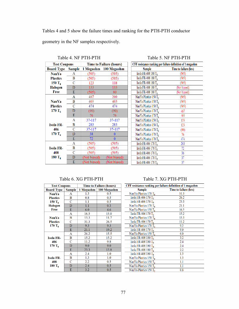
77
Tables 4 and 5 show the failure times and ranking for the PTH-PTH conductor
geometry in the NF samples respectively.
Table 4. NF PTH-PTH Table 5. NF PTH-PTH
Table 6. XG PTH-PTH Table 7. XG PTH-PTH

78
Tables 6 and 7 show the failure times and ranking for the PTH-PTH in the XG
samples, smallest conductor spacing, where samples labeled A, B and C were biased
at 2 volts and D and E were biased at 1 volt. The failure times appear to be random,
most likely due to the random defects playing more of role in the time to failure at
smaller spacings as opposed to the path formation in larger spacings.
6.4 Failure Analysis
After failure of the samples in the first set (NF) due to resistances drop to 1 megaohm
(the resistance of the in-series protection resistor), selected samples were sent to
Neocera to conduct SQUID to determine if there were indeed failures, and if so,
where were the locations. One of the samples that failed early in the test, an Isola FR-
406, was analyzed using the SQUID to confirm and locate the short due to conductive
filament formation. Figure 51 shows the SQUID output, locating the shorted sites in
the board, in both the PTH-PTH and PTH-power plane conductor geometries.
Figure 51. The SQUID output shows the current mapping images, verifying that there were short circuits and determining their locations respective to the board conductors.

79
After the short circuits were identified, cross-sectional techniques were employed to
locate the defects responsible for the shorts and allow examination of the defective
areas using optical and E-SEM microscopy.
Figure 52. SQUID mapping and respective conductor locations identified for cross-sectioning.
Figure 53. Prior to reaching the failure site, circular blue/black areas, possibly Cu(OH)2 due to the copper reaction with water, were observed.
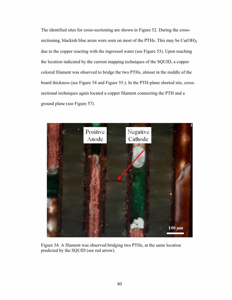
80
The identified sites for cross-sectioning are shown in Figure 52. During the cross-
sectioning, blackish blue areas were seen on most of the PTHs. This may be Cu(OH)2
due to the copper reacting with the ingressed water (see Figure 53). Upon reaching
the location indicated by the current mapping techniques of the SQUID, a copper
colored filament was observed to bridge the two PTHs, almost in the middle of the
board thickness (see Figure 54 and Figure 55.). In the PTH-plane shorted site, cross-
sectional techniques again located a copper filament connecting the PTH and a
ground plane (see Figure 57).
Figure 54. A filament was observed bridging two PTHs, at the same location predicted by the SQUID (see red arrow).

81
Figure 55. This optical micrograph shows an enlargement of the shorted site.
Figure 56. Current mapping of one of the failed XG samples at the PTH-PTH grid shows that the current follows the grid pattern, and contains many leakage paths; not only one leakage path as in the CFF validated failures. It is possible that this was the same failure mechanism observed in the early failing AF samples as well. E-SEM examination of the localized failure site revealed delamination at the fiber-
epoxy interfaces in areas immediately surrounding the failure site (see Figure 59).

82
Figure 57. This optical photo shows a copper filament bridging a PTH and ground plane at the precise location predicted by the SQUID.
Figure 58. EDS analysis of a cross-sectioned site perpendicular to the filament showed copper in the shorted location.
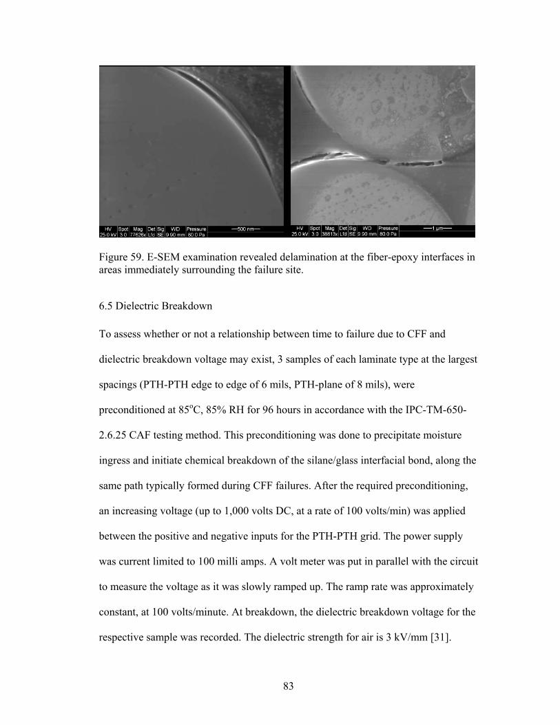
83
Figure 59. E-SEM examination revealed delamination at the fiber-epoxy interfaces in areas immediately surrounding the failure site.
6.5 Dielectric Breakdown
To assess whether or not a relationship between time to failure due to CFF and
dielectric breakdown voltage may exist, 3 samples of each laminate type at the largest
spacings (PTH-PTH edge to edge of 6 mils, PTH-plane of 8 mils), were
preconditioned at 85oC, 85% RH for 96 hours in accordance with the IPC-TM-650-
2.6.25 CAF testing method. This preconditioning was done to precipitate moisture
ingress and initiate chemical breakdown of the silane/glass interfacial bond, along the
same path typically formed during CFF failures. After the required preconditioning,
an increasing voltage (up to 1,000 volts DC, at a rate of 100 volts/min) was applied
between the positive and negative inputs for the PTH-PTH grid. The power supply
was current limited to 100 milli amps. A volt meter was put in parallel with the circuit
to measure the voltage as it was slowly ramped up. The ramp rate was approximately
constant, at 100 volts/minute. At breakdown, the dielectric breakdown voltage for the
respective sample was recorded. The dielectric strength for air is 3 kV/mm [31].

84
Based on the PTH-PTH spacing of 6 mils (0.1524 mm), it would take 450 volts to
cause an arc across this gap. The PTHs were solder-mask defined, (solder mask
covering the air gap between the PTHs) and breakdown voltages varied from 670 to
over 999 volts, discrediting that the dielectric breakdown was due arcing across the
air. If the breakdown were due to arcing across air, all values would center around
450 volts, not varying from 670 up to over 999 volts.
The specification governing solder mask dielectric strength is a minimum breakdown
voltage of 500 VDC/mil [32]. For 6 mils, the solder mask should be able to withstand
at least 3,000 volts, far above of what was applied. Therefore, dielectric breakdown
was most likely due to an internal breakdown of the dielectric epoxy glass matrix,
weakened by moisture ingress. Table 8 shows the dielectric breakdown voltage for
each of the samples tested. The values suggest that in a best to worst ranking, the
order is:
Nanya Plastics 170 > Nanya Plastics 150 > Isola FR406 > Isola FR408
This ranking follows the same trend as the PTH-PTH 10 volt test bias failure data,
implying that dielectric breakdown voltage may be a possible indicator of a PWB’s
resistance to CFF. The arrangement of photos in Figure 60 shows the internal damage
to one of the boards occurring as a result of the dielectric breakdown voltage testing.
Table 8. Dielectric breakdown

85
Figure 60. Photos show the damage to the PTH as a result of the dielectric voltage breakdown testing. A t-test was used to examine the statistical differences among the 4 sets of values
obtained from the dielectric breakdown voltage tests. The equation used is:
nms
yxt
p11
+
−= (18)
where x and y are respective sample averages, sp is the pooled estimator and m and n
are respective sample sizes. Sp2 is calculated by:
( ) ( )2
11 22
212
−+⋅−+⋅−
=nm
SnSmS p (19)
Using equations 18 and 19, along with the values from Table 8, the t values obtained
for the paired comparisons, along with the confidence level, show that there is a
distinguishable difference between the respective pairs, as shown in Table 9. It can be
concluded with 90% confidence that there is a difference between the samples in the
last four rows. In other words, the values obtained from the dielectric breakdown
tests, may reveal the relative susceptibility of a PWB type to CFF.

86
Table 9. Paired t-test values
B o a r d T y p e s C o m p a r e d T value Reject or accept at 90 %
I s o l a F R - 4 0 6 I s o l a F R - 4 0 8 1.33 Less than 90% confidence in difference
NanYa Plastics 150 NanYa Plastics 170 1.09 Less than 90% confidence in difference
I s o l a F R - 4 0 6 NanYa Plastics 150 2.80 More than 90% confidence in difference
I s o l a F R - 4 0 6 NanYa Plastics 170 3.56 More than 90% confidence in difference
I s o l a F R - 4 0 8 NanYa Plastics 150 7.22 More than 90% confidence in difference
I s o l a F R - 4 0 8 NanYa Plastics 170 9.97 More than 90% confidence in difference

87
CHAPTER 7: PATH FORMATION
Prior to formation of the filament, consistent with the published literature, a pathway
connecting the oppositely biased conductors must be formed. Some of the more
common pathways are show in Figure 61 Other path configurations include formation
between PTHs and power/ground planes, between internal traces, between an internal
trace and a PTH, and between internal and surface traces.
It is hypothesized that path formation, which is proposed to be voltage independent, is
the rate-limiting step in conductive filament formation. In other words, it takes a
much longer time for the pathway to be formed than for the metal migration and
formation of the conductive filament bridging and shorting the two conductors. This
chapter discusses the different ways in which this path may be formed.
Figure 61. Three common CFF pathway configurations
88
7.1 Modes of Path Formation
7.1.1 Mechanical Degradation
One mode of path formation is mechanical degradation or physical delamination at
the interfaces of the glass fibers and epoxy resin matrix. Mechanical stress can arise
due to the coefficient of thermal expansion (CTE) mismatches in the properties of the
epoxy resin and the glass fibers. Epoxy resin has a CTE of approximately 60 ppm/oC,
while that of the glass fibers is around 5 ppm/oC. This mismatch can lead to high
interfacial stresses and debonding at the fiber-resin interface during thermal cycling
[15]. The interfacial debonding observed by Li et al. was more severe at the outer
fibers in the bundles. Manufacturing defects, as discussed in Chapter 3, can accelerate
and help to initiate the formation of this pathway.
The difference in the moisture absorption of glass fibers and epoxy resin can also lead
to interfacial stresses. During thermal-humidity cycling, the swelling and shrinking of
the epoxy has been shown to induce physical debonding at the fiber glass/epoxy resin
interface, in addition to micro-cracking in the resin. The absorption of moisture can
also reduce the Tg of the laminate, allowing excess thermal stress to cause more
damage. Path formation, where there is a physical, mechanical separation at the fiber
glass/epoxy resin interface or micro-cracking due to thermal cycling and thermal-
humidity cycling, is not reversible.

89
7.1.2 Chemical Degradation
A pathway between conductors may also be formed by chemical hydrolysis of the
silane glass finish or coupling agent. Studies indicate that the glass epoxy interface
absorbs 5 to 7 times more moisture than the bulk epoxy [16]. The most common
cross-linking agent used in FR-4 and many other epoxy-based laminated systems is
dicyandiamide (aka dicy). Dicy is hydrophilic and to some extent, so is the glass
surface. This combination of a hydrophilic surface and a hydrophilic cross-linking
agent appears to be one of the factors responsible for the mechanism where by
chemical degradation of glass fiber/epoxy resin interface due to hydrolysis occurs.
Varnell et al. has shown that PWBs manufactured with non-dicy cross-linked epoxy
resins exhibit much more resistance to CAF failures compared to PWBs
manufactured with dicy cross-linked epoxy resins [17]. Research by Lando et al.
demonstrated that this type of chemical degradation might be reversible.
7.1.3 Hollow Fibers
During the manufacture of glass fibers, a homogeneous melt composition with
negligible impurities is necessary to prevent the decomposition of raw materials. The
sublimation of these organics can lead to trapped gases. Depending on the viscosity of
the glass mixture and various manufacturing processes, these gases can get trapped as
bubbles, called seeds. Seeds are a naturally occurring part of the process and thus
methods to remove them are necessary. If the molten glass contains a sufficient level
of impurities, air bubbles may become trapped inside the fibers while being drawn
through the bushing. These air bubbles, unless very large, do not cause fiber breakage
but end up as capillaries in the glass fibers, otherwise known as hollow fibers. These
90
hollow glass fibers increase the opportunity for failure between close conductors
because the capillary provides a convenient path for the formation of conductive
filaments. As discussed earlier in Chapter 4, hollow fibers pose a serious reliability
threat in that they can remove the rate limiting step, T1, from the proposed two step
sequential process, T1 consisting of path formation, followed by T2 the
electrochemical reaction, where T1 >> T2 [5], [6].
7.1.4 Vertical Filament Formation
In a set of PWBs failing by shorted internal planes, verification of the hypothesized
root-cause required actual physical identification of a hydrolyzed Cab-o-sil particle at
a failure site. Unfortunately, this was made difficult by large area covered by the
power and ground planes, which made identification of the failure site using
functional or parametric testing literally impossible. Visual inspection was also
difficult due to the absence of a controlled burn area. The high glass transition
temperature (Tg) of the dielectric material, 180oC, makes it relatively resistant to high
temperatures. Therefore, an internal temperature rise to 200oC can result in solder
reflow in the PTH's, but will not visibly damage the dielectric material. The
temperatures necessary to ignite Megtron material may be so high as to result in
thermal runaway. The effect is binary: failed boards will either have no visible
charring or will have large areas of the board severely burned, with any evidence of
root-cause destroyed. Either case will tend to hide the physical object causing the
electrical short.

91
This behavior also prevented the use of thermal imaging, since the energy required to
dissipate sufficient heat also tended to result in damage to the failure site. The
solution was to modify a procedure used at CALCE to identify very small voids that
bridge ceramic capacitors and cause current leakage. The resistance between a power
and ground pin were monitored as the board was sectioned. Using a binary approach,
the potential failure site was narrowed to a very small area. This area was very slowly
ground and polished until a change in resistance was observed.
During several attempts to observe a non-damaged failure site, a large angular
particle was identified at a failure site. The images are displayed in Figure 62, Figure
63 and Figure 64. One additional non-damaged failure site was identified. This board
contained a 4-mil core between power and ground, as opposed to the 2-mil core
material that was experiencing field failures. The images seem to show a particle of
similar coloring as that seen in the board with the 2-mil core.
Figure 62. Optical micrograph, under brightfield lighting, of a void observed during cross sectioning of a board.

92
Figure 63. Optical micrograph, using differential interference contrast, of a vertical cross-section of the board. The filler agglomerate has maximum dimension of 3.5 mil (87 microns). A yellow arrow marks what appear to be nodules of copper emanating from layer 10 (power). Since the spacing between the power and ground plane is only 2 mils (~50.8
microns), particles exceeding this size would bridge layers 10 and 11. However,
bridging alone does not explain the electrical failure seen in the printed wiring boards.
This is because silica-based particles are electrically insulative. An additional
mechanism, known as electrochemical migration (ECM) is required.
A Scanning SQUID Microscope is a sensitive near-field magnetic imaging system.
This microscope can image buried current-carrying wires by measuring the magnetic
fields produced by the currents, or it can be used to image fields produced by
magnetic materials. By mapping the current in an integrated circuit or a package,

93
short circuits can be localized and designs can be verified to ensure that charge is
flowing where expected. MAGMA-C10 uses a high temperature SQUID with a
sensitivity of 20 picotesla or two million times smaller than the Earth’s magnetic
field. The microscope has been designed to keep a high temperature SQUID cooled
below 80K and in vacuum while the device under test (DUT) is at room temperature
in air. The unique design of MAGMA-C10 also enables the SQUID to be positioned
as close as 50 mm from the DUT. Even though the SQUID is not in a magnetically
shielded environment, the sensitivity is high enough to image currents as small as 600
nA at a 100 mm working distance with 30 ms averaging.
Figure 64. Optical micrograph of a vertical cross-section showing what appears to be a nodule in the PWB. The magnetic field produced by a sample can be imaged by rastering the sample in
close proximity to the SQUID. If the sample contains a permanent magnetic field, as

94
Figure 65. Particle observed in the center of a “mound” in many land grid arrays and lead frames, the microscope will map out this constant
or “DC” magnetic field. In addition, electric currents in the device produce magnetic
fields. The presence of a short circuit in an electrical part typically appears as a very
strong concentration of magnetic field strength, with the field in opposite directions to
either side of the short.
During non-contact imaging of room temperature samples in air, the system achieves
a raw, unprocessed spatial resolution equal to the distance separating the sensor from
the current, or the effective size of the sensor (~30 microns for a standard SQUID
tip), whichever is larger. To best locate a short in a buried layer, however, a Fast
Fourier Transform (FFT) back-evolution technique can be used to transform the

95
magnetic field image into an equivalent map of the current in an integrated circuit or
printed wiring board. The resulting current map can then be compared to the circuit
diagram to determine the fault location. With this post-processing of a magnetic
image and the low noise present in SQUID images, it is possible to enhance the
spatial resolution by factors of 5 or more over the near-field limited magnetic image.
This enhanced resolution describes how well a scanning SQUID microscope can
resolve current paths in a sample. The system’s output is displayed as a false-color
image of magnetic field strength or current density (after processing) versus position
on the sample.
Figure 66. An area containing a particle bridging two copper planes is shown.

96
7.2 Use of SQUID Microscopy in Detecting VFF
SQUID microscopy was performed on failure sites identified in Figure 65. The results
for the 2-mil core are shown in Figure 66. The results demonstrate that current is
flowing through the particle, verifying that the identified particle is the location of the
short circuit. The results for the 4-mil core are shown in Figure 67. These results
demonstrate that the horizontal and vertical location of the short strongly corresponds
to the location of the hydrolyzed Cabosil particle.
Figure 67. Particle seen in material, bridging two copper planes.

97
CHAPTER 8: GLASS-SILANE-EPOXY BONDING AND
DEBONDING
8.1 Voltage Dependency of Glass-Epoxy Interfacial Adhesion
The previous chapters detailed the results of the experimental investigation on
conductive filament formation behavior as a function of applied voltage, conductor
geometry, and conductor spacing. Of particular interest from the experimental results
was the broad range of failure times among similar coupons tested under the same
environmental conditions. Specifically, within one material set at an applied potential
of 10 VDC, one coupon failed after approximately 18 minutes while a second coupon
experienced no failure after 500 hours of exposure to the same conditions. The large
discrepancy initially suggested that within the first coupon was a pre-existing path,
potentially due to manufacturing defects, while the second coupon was relatively
resistant to path formation. The second coupon did experience relatively rapid failure,
within two hours, after the application of 50 VDC. Nominally, this type of extreme
change in failure behavior would not be expected, as most of the time-to-failure
models within the literature indicate a linear dependence on voltage. Therefore, an
increase in the voltage by a factor of 5 should result in the equivalent drop in time to
failure. A much more abrupt change in behavior, by approximately two orders of
magnitude, seems to suggest that the presence of an electric field may accelerate the
process of path formation. The purpose of this section is to provide an analytical
discussion of the potential mechanisms by which electric energy would initiate or

98
accelerate path formation, within the framework of the degradation of the fiber/matrix
interfacial bond.
Numerous discussions in prior work on conductive filament formation have
repeatedly emphasized that the time required to induce path formation between the
glass fiber reinforcement and the epoxy matrix is the rate limiting step in regards to
time to product failure [5]. As mentioned in the previous chapters, variants have been
identified that allow for the immediate migration of conductive filaments within the
laminate structure. These variants included manufacturing defects, such as micro-
cracking along the fiber/matrix interface, hollow fibers, and the presence of vertical
paths. While the characterization of these path variants is critical to the furthering the
knowledge base on conductive filament formation, the primary focus in industrial and
scientific investigations has been on the degradation of the fiber glass to epoxy resin
bonding, which allows for the creation of a physical path after some latency period.
It has been theorized that this degradation mechanism is the hydrolysis of the
organosilanes used as an adhesion promoter on the surface of the glass fiber. While
there are numerous definitions of silanes, and more specifically organosilanes, for the
purposes of this dissertation they will defined as a bi-functional molecule with the
chemical formulae Y-(CH2)n-Si(OX)3, where Y is an organo-functional group and
OX is a silicon-functional group [19]. During glass fiber manufacture, the
organosilanes are applied as a component of a surface solution called a size. In the
presence of water, the silicon function group hydrolyzes, forming a silanol group,

99
Si(OH)3, that chemically reacts with the hydroxyl groups on the surface of the glass
to form a network of siloxane bonds (Si-O-Si) [20]. A schematic of this process is
provided in Figure 68. The organo-functional group then reacts with the epoxy matrix
during the curing process, creating a physio-chemical bond.
Figure 68. Schematic of reaction between organosilane and glass surface
The degradation reaction of concern, hydrolysis of silane bonds after long-term
exposure to elevated temperature/humidity conditions, is simply a reversal of siloxane
reaction, as per
SiOH + SiOH ↔ Si2O + H2O
The use of this reaction to describe path formation in conductive filament formation
is an expected result. Hydro-thermal degradation of silane bonds in glass/epoxy
composites is well known [21-25] and provides a basis for the latency period often
observed during experimental measurements. As a result, the previous investigations
100
into conductive filament formation have claimed that path formation due to
hydrolysis is the rate-limiting step in product failure.
A number of investigators have also attempted to provide a life model to describe
time to failure behavior [7, 9, 10, 14]. These models, detailed in Chapter 2, are
primarily empirically-based, and contain a number of environmental parameters,
including voltage, distance, temperature and moisture. An interesting contradiction is
the presence of voltage within the life models. Within the process of corrosion at the
anode, the presence of a voltage is justifiable as the rate of oxidation is directly
proportional to electromotive force (EMF). Within the process of metal migration, the
presence of an electric field term, voltage normalized by anode-to-cathode separation,
can be rationalized by the electric field applying the force that induces the metallic
ions to move towards the cathode. However, if, as previously mentioned, path
formation is the rate-limiting step, the influence of voltage has not been clearly
explained in regards to mechanisms occurring at the molecular-level.
8.2 Chemistry of Glass-Silane-Epoxy Interfacial Bonding
Epoxy/silane/glass bonding occurs in three steps – hydrolysis of the silane,
condensation of the hydrolyzed silane on the glass, and coupling of the epoxy to the
hydrolyzed silane. The silane is usually of the form XSiY3, where X is an
organofunctional group and Y is a hydrolysable functional group.
Glycidoxypropyltrimethoxysilane and aminopropyltriethoxysilane are common
examples. Both have n = 1 and all four hydrogens replaced by functional groups.

101
Glycidoxypropyltrimethoxysilane:
CH 3 – O \ CH 3 – O – Si – CH 2 – CH 2 – CH2 – O – CH2 – CH – CH2 / \ / CH 3 – O
O
Aminopropyltriethoxysilane:
CH3 – CH2 – O \ CH3 – CH2– O – Si – CH2 – CH2 – CH2 – NH2 / CH3 – CH2 – O
Hydrolysis of the silane takes place as follows:
CH3 – O \ CH3 – O – Si – CH2 – CH2 – CH2 – O – CH2 – CH – CH2 + 3 HOH / \ / CH3 – O O water
HO \ HO – Si – CH2 – CH2 – CH2 – O – CH2 – CH – CH2 + 3 H3OH / \ / HO O methanol
OR
CH3 – CH2 – O \ CH3 – CH2– O – Si – CH2 – CH2 – CH2 – NH2 + 3 HOH / CH3 – CH2 – O water
HO \ HO – Si – CH2 – CH2 – CH2 – NH2 + 3 CH3 – CH2 –OH / HO ethanol

102
To understand the condensation of the hydrolyzed silane on the glass, it must be
understood that in silica, each silicon atom is covalently bonded to four oxygen
atoms, each of which is covalently bonded to another silicon atom. Thus, each oxygen
atom is shared between two silicon atoms, contributing ½ of an oxygen atom to each
silicon atom. Four ½ atoms of oxygen per silicon are the same as two atoms of
oxygen per silicon, giving silica the formula SiO2. At the surface, however, there is
one oxygen per silicon atom that is not bonded to any other atom – a dangling bond,
as shown below in Figure 69.
.
| Exterior O | Interior Si / | \ O O O | | | Si Si Si / | \ / | \ / | \
Figure 69. Schematic showing each dangling bond attached to a hydrogen atom.
103
A similar phenomenon occurs for the other constituents of the glass at the surface,
resulting in a surface consisting of hydroxyl groups. The condensation of the
hydrolyzed silane on the glass occurs as follows:

104
HO
\ 3 Si – OH + H O – Si – CH 2 – CH2 – CH2 – O – CH2 – CH – CH2 / \ /
glass HO silane O
Si – O \ Si – O – Si – CH 2 – CH 2 – CH2 – O – CH2 – CH – CH2 + 3 HOH / \ / Si – O
O
glass silane water
OR HO
\ 3 Si – OH + HO – Si – CH 2 – CH2 – CH2 – NH2 / glass HO silane
Si – O \ Si – O – Si – CH 2 – CH 2 – CH2 – NH2 + 3 HOH / Si – O glass
water silane
Note that the silicon atom in the silane is now bonded to the silicon atoms in the glass
through oxygen atoms – as the silicon atoms in the glass are bonded to each other. If
the water produced in the forward reaction is continuously removed, by evaporation
for instance, the bonding of silane to glass will continue until either there is no more
silane or no more attachment sites on the glass surface. Conversely, if water is added
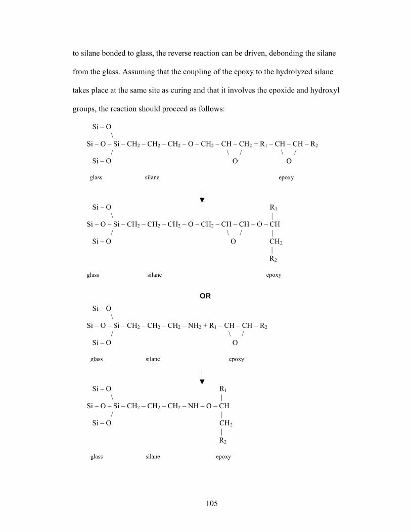
105
to silane bonded to glass, the reverse reaction can be driven, debonding the silane
from the glass. Assuming that the coupling of the epoxy to the hydrolyzed silane
takes place at the same site as curing and that it involves the epoxide and hydroxyl
groups, the reaction should proceed as follows:
Si – O \ Si – O – Si – CH2 – CH2 – CH2 – O – CH2 – CH – CH2 + R1 – CH – CH – R2 / \ / \ / Si – O O O glass silane epoxy
Si – O R1 \ | Si – O – Si – CH2 – CH2 – CH2 – O – CH2 – CH – CH – O – CH / \ / | Si – O O CH2 | R2 glass silane epoxy Si – O \ Si – O – Si – CH2 – CH2 – CH2 – NH2 + R1 – CH – CH – R2 / \ / Si – O O glass silane epoxy
Si – O R1 \ | Si – O – Si – CH2 – CH2 – CH2 – NH – O – CH / | Si – O CH2 | R2 glass silane epoxy
OR
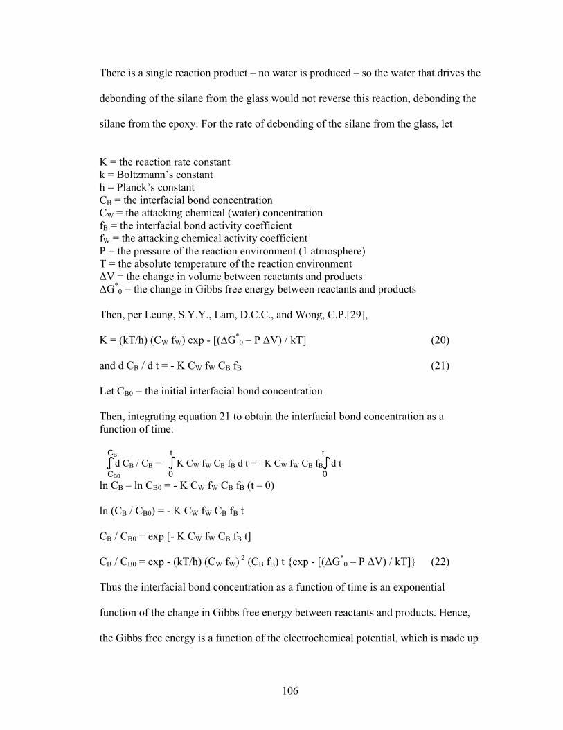
106
There is a single reaction product – no water is produced – so the water that drives the
debonding of the silane from the glass would not reverse this reaction, debonding the
silane from the epoxy. For the rate of debonding of the silane from the glass, let
K = the reaction rate constant k = Boltzmann’s constant h = Planck’s constant CB = the interfacial bond concentration CW = the attacking chemical (water) concentration fB = the interfacial bond activity coefficient fW = the attacking chemical activity coefficient P = the pressure of the reaction environment (1 atmosphere) T = the absolute temperature of the reaction environment ∆V = the change in volume between reactants and products ∆G*
0 = the change in Gibbs free energy between reactants and products Then, per Leung, S.Y.Y., Lam, D.C.C., and Wong, C.P.[29], K = (kT/h) (CW fW) exp - [(∆G*
0 – P ∆V) / kT] (20) and d CB / d t = - K CW fW CB fB (21) Let CB0 = the initial interfacial bond concentration Then, integrating equation 21 to obtain the interfacial bond concentration as a function of time:
CB t t d CB / CB = - Κ CW fW CB fB d t = - Κ CW fW CB fB d t CB0 0 0
ln CB – ln CB0 = - K CW fW CB fB (t – 0) ln (CB / CB0) = - K CW fW CB fB t CB / CB0 = exp [- K CW fW CB fB t] CB / CB0 = exp - (kT/h) (CW fW) 2 (CB fB) t {exp - [(∆G*
0 – P ∆V) / kT]} (22) Thus the interfacial bond concentration as a function of time is an exponential
function of the change in Gibbs free energy between reactants and products. Hence,
the Gibbs free energy is a function of the electrochemical potential, which is made up
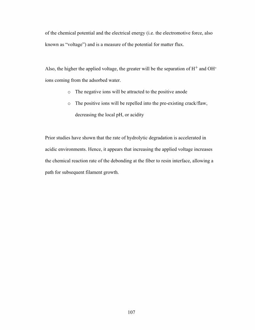
107
of the chemical potential and the electrical energy (i.e. the electromotive force, also
known as “voltage”) and is a measure of the potential for matter flux.
Also, the higher the applied voltage, the greater will be the separation of H+ and OH-
ions coming from the adsorbed water.
o The negative ions will be attracted to the positive anode
o The positive ions will be repelled into the pre-existing crack/flaw,
decreasing the local pH, or acidity
Prior studies have shown that the rate of hydrolytic degradation is accelerated in
acidic environments. Hence, it appears that increasing the applied voltage increases
the chemical reaction rate of the debonding at the fiber to resin interface, allowing a
path for subsequent filament growth.

108
CHAPTER 9: OBSERVATIONS AND CONTRIBUTIONS
9.1 Observations
When the DC voltage bias is removed shortly after a failure is detected, the short can
disappear, even if the samples are kept in the high temperature/high humidity
environment (85 C, 85% RH), especially for the PTH-plane failures. This suggests
that the copper ions may be still mobile in the initial stages of failure and still need
voltage bias as a driving force to maintain the location of the copper ions.
For PWB conductor spacings 4 mils or less, the IPC TM-650 CAF test may not be
suitable, as there were instantaneous failures in the samples with conductor spacings
4 mils and less. These failures were not due to CFF as shown by the SQUID.
Extensive optical and E-SEM microscopic examinations of cross-sectioned areas, in
close proximity to and far away from the failure sites, revealed that there was
degradation only in the vicinity of the failure.
Comparison of the time to failure for the different spacings shows that boards, which
survive the longest at the larger spacings, may not necessarily survive the longest for
closer spacings. At closer spacings, defects such as wicking and damage due to
drilling have a greater impact, whereas for the larger spacings, interfacial-bonding
strength may be the controlling parameter.
Examination of the PTH-PTH dielectric breakdown voltage values after exposure of
the test boards to 85 C, 85% RH for 96 hours shows that the trend follows the time to

109
failure observed for the PTH-PTH failure data, NY 170>NY 150> IS FR408 and IS
FR406. This suggests that dielectric breakdown voltage could be an indicator of CFF
susceptibility.
Board types that show the longest time to failure due to CFF in PTH-PTH
configuration, may not necessarily offer the best protection for PTH-plane geometry.
PTH-PTH CFF resistance experimentally found was NY 170>NY 150> IS FR408
and IS FR406, but PTH-plane CFF resistance was IS FR408> NY 170 and NY 150>
IS FR408.
Industry uses one of three failure criteria to determine a failure definition:
o Hard short (1 x 10⁶ ohms, permanent)
o Decade drop in resistance (TM-650, 2.6.25)
o Less than 100 Megaohms (IPC/EIA J-STD-001C)
As seen in the time to failure data for the samples tested, the failure criteria selected
can have a significant impact on the time to failure, as per the definition.
The IPC-TM-650 test specification of monitoring every 24 – 100 hours may allow
intermittent failures to go undetected, as seen in the cases where intermittent drops in
insulation resistance may last only 5 – 6 minutes and then fully recover.
9.2 Contributions
1. Identified a failure involving a hollow fiber, filled with copper colored
material bridging and shorting two PTHs, verifying that hollow fibers can lead
to CFF failures

110
2. Applied a hollow fiber detection technique used in detecting leaks in pressure
vessels and modified it to allows the detection of hollow fibers within printed
wiring boards
3. Developed a failure probability equation based on hollow fiber concentration,
which allows the calculation of a critical hollow fiber concentration for an
acceptable reliability, based on board and conductor parameters
4. Developed a hollow fiber assessment standard screen, allowing board
fabrications and contract assemblers to qualify suppliers and discard lots with
hollow fiber concentrations above acceptable specifications
5. Discovered a new type of “vertical” filament formation, migrating in different,
vertical path through cabosil, rather than along the traditional horizontal fiber-
epoxy delaminated interface
6. Demonstrated the use of the scanning superconducting quantum interference
device (SQUID) in detecting and locating short circuit paths due to CFF by
analyzing the failures in the test boards in this study.
7. Experimentally demonstrated that the specification on monitoring insulation
resistance (24 – 100 hours) used in the current industry standard IPC-TM-650-
is insufficient for capturing intermittent failure occurrences, as seen in some
of the intermittent failures lasting for durations of less than 6 minutes
111
8. Showed that the IPC industry standard for CFF testing of PTH-PTH conductor
spacings of 4 mils or less, at 85oC/85% RH can introduce a failure mechanism
other than CFF

112
CHAPTER 10: SUMMARY
The electronics industry has recognized that failure due to conductive filament
formation in printed circuit boards is a problem. To address this issue, organizations
such as the National Physical Laboratory spend up to 3 million dollars annually to
characterize these failures. IPC has also developed testing standards to evaluate a
printed wiring board’s susceptibility to conductive filament formation failures. Board
fabricators, in an attempt to mitigate the risks of printed wiring failures due to this
phenomenon have fabricated “CFF resistant laminates”.
Previous researchers (discussed in Chapter 2) have developed time to failure models,
which are empirically derived, rather than based on physics of failure. There is also a
voltage term in each of these equations. The time to failure due to conductive
filament formation, is divided in two sequential steps:
t1 – the time for path formation, and
t2 – the time for the electrochemical reaction or filament growth, where t1 >>t2
Since the rate-limiting step (t1) the time for the path formation is much longer than t2,
the time for the conductive filament growth (t1 >>t2), t2 may be negligible. Lando in
1979 postulated that the formation of the path (t1) was independent of voltage.
However, the time to failure models, all contain a voltage parameter, and basically
predict the time for the rate-limiting step (reported by Lando to be voltage

113
independent). There is a contradiction since this rate-limiting step is voltage
independent.
In this dissertation, it was shown that voltage, but more so the electric field (a
combination of voltage and conductor spacing), plays a role in the rate at which the
path is formed due to a relationship to the Gibbs free energy, and the polar nature of
the water molecule.
To give more insight into the overall understanding of this failure mechanism,
specifically in how the rate-limiting step - the formation of a path – is created,
different variations of path formation were investigated.
Optical and electron microscopic examinations of failure sites due to conductive
filament formation show that the formed path is typically along debonded or
delaminated fiber glass/epoxy resin interfaces, due to breaking of the silane bonds.
The silane bonds can be chemically degraded by hydrolysis (adsorption of water at
the fiber glass/epoxy resin interface) or by repeated thermal cycling, which induces
stresses at the interface due to a CTE ration mismatch of 1 to 12 (5 ppm/oC – E fiber
glass, 60 ppm/oC – FR-4 epoxy resin). The formation of these types of paths take
some finite amount of time, since the moisture absorption or thermal cycling is
necessary for the eventual breaking/degradation of the bonds at the interface,
allowing a path between conductors. However, two new variants of path formation
were discovered and examined. These new variations are:

114
1. Formation through hollow fibers (discussed in Chapter 4) and,
2. Vertical formation through cracked silica particles (Chapter 7)
With these two new variants, t1 – the time for path formation and rate limiting step, is
zero, as the path is already present prior to operation or testing of the printed wiring
assembly. Hence, the time to failure is only t2 – the time for the electrochemical
reaction or filament growth, where t1 >>t2, and can be orders of magnitude shorter
since there is a pre-existing path. For products which may be used in harsh
environments (high temperature and humidity) such as avionics, automotive, military
and medical, where reliability is critical, there should be screens/acceptance criteria in
place to ensure that these manufacturing related defects which can significantly
shorten the time to failure due to CFF and put lives in jeopardy. A methodology to
detect and screen hollow fibers was developed and an example of how it can be
implemented based on an acceptable level of reliability is given in Chapter 4.
The accelerated tests in this study were conducted using boards designed with the
smallest conductor spacings ever tested (as small as 2 mils distances between
oppositely biased conductors). Subjecting the boards to tests as prescribed by the IPC
standard for CFF testing showed that other failure mechanisms can be introduced as
well as failures due to CFF being missed by the monitoring frequency specification of
every 24 to 100 hours. Due to the intermittent nature of CFF failures, (some in this
study lasted for only 5 minutes), unless there is continuous monitoring of the
resistance between conductors of interest, some failures may fall through the cracks,

115
especially those of short durations. Hence, another test method to address the
continuously shrinking feature sizes that will eventually reach 2 mils, and correctly
assess a laminate’s robustness to CFF failures needs to be developed.
These tests also showed that for the FR-4 type of laminates and feature sizes used,
there could be failures in less than 40 hours in conditions as harsh as 85 oC/85% RH
as seen by the insulation resistance monitoring of the 4 and 3 mil spacings. Other
materials or designs will have to be incorporated as feature sizes shrink while the use
in and exposure to harsh environments (such as lead free reflow profiles) increase.
An observation from a set of tests shows that dielectric voltage breakdown values
may be an indicator of the resistance of a laminate to CFF failure. This has the
potential to save time and money due to the expensive equipment needed for the
monitoring setup and the length of time (500 hours or ~ 3 weeks) required for the
testing.

116
CHAPTER 11: FUTURE WORK
It has been shown that increasing the voltage can increase the rate of path formation.
Subsequent CFF investigations, which focus on the characterization of hydrolytic
degradation of silanes under a range of applied voltages and electric fields, should be
completed. The results of these tests can give information on the relationship between
voltage and path formation.
Tests show that there may be a relationship between dielectric breakdown and time to
failure due to CFF. A follow up study consisting of a broad range of testing should be
performed to assess how predictable is the relationship between dielectric breakdown
and susceptibility to CFF. A design of experiments should also be carried out to
determine and optimize the duration of time and humidity/temperature parameter
settings necessary to initiate path degradation so that dielectric breakdown can occur
along the “weakened” path, simulating CFF.
Tests using the same boards should be run at other temperature and relative humidity
environments to determine and validate the acceleration factors and determine which
accelerated test environments may be applicable for feature spacings less than 4 mils
to induce CFF failures.
Some tests have indicated that time to failure is dependent on the direction of the
fabric weave along which the path is formed. Accelerated tests should be run along
different orientations of the fiber weave to evaluate the increase or decrease in time to

117
failure that can be expected for conductors which are parallel, perpendicular, and at
45 degree angles to the machine weave of the fabric.

118
REFERENCES
1. Boddy, P.J., Delany, R.H., Lahti, J.N., Landry, E.F. and Restrick, R.C.
“Accelerated Life Testing of Flexible Printed Circuits,” 14th International
Reliability Physics Symposium, 1976, pp. 108-116.
2. Electrochemical Migration: Electrically Induced Failures in Printed Wiring
Assemblies, IPC-TR-476A, The Institute for Interconnecting and Packaging
Electronic Circuits, Northbrook, IL, IPC 1997.
3. Kohman, G.T., Hermance, H.W. and Downes, G.H. “Silver Migration in
Electrical Insulation,” The Bell Technical Journal, Nov. 1955, p. 1115.
4. Lathi, J.N., Delaney, R.H. and Hines, J.N. “The Characteristic Wear-out Process
in Epoxy Glass Printed Circuits for High Density Electronic Packaging,”
Reliability Physics, 17th Annual Proceeding, 1979, pp. 39–43.
5. Lando, D.J., Mitchell, J.P. and Welsher, T.L. “Conductive Anodic Filaments in
Reinforced Polymeric Dielectrics: Formation and Prevention,” Reliability
Physics, 17th Annual Proceeding, 1979, pp 51–63.
6. Welsher, T.L., Mitchell, J.P. and Lando, D.J. “CAF in Composite Printed-Circuit
Substrates: Characterization, Modeling, and a Resistant Material,” Reliability
Physics, 18th Annual Proceeding, 1980, pp 235–237.
7. Mitchell, J.P. and Welsher, T.L. “Conductive Anodic Filament Growth in Printed
Circuit Materials,” Proceedings of the Printed Circuit World Convention II, 1981,
pp. 80-93.
119
8. Augis, J.A., DeNure, D.G., LuValle, M.J., Mitchell, J.P., Pinnel, M.R. and
Welsher, T.L. “A Humidity Threshold for Conductive Anodic Filaments in Epoxy
Glass Printed Wiring Boards”, 3rd International SAMPE Electronics Conference,
1989, pp. 1023-1030.
9. Rudra, B.S. and Pecht, M.G. “Assessing Time-to-Failure Due to Conductive
Filament Formation in Multi-Layer Organic Laminates,” Packaging and
Manufacturing Techniques, Part B, Vol. 17, No. 3, 1994, pp. 269-276.
10. Sauter, K. “Electrochemical Migration Testing Results: Evaluating PWB Design,
Manufacturing Process, and Laminate Material Impacts on CAF Resistance,
CircuiTree, July, 2002.
11. Ready, W.J., Turbini, L.J., Stock, S.R. and Smith, B.A. “Conductive Anodic
Filament Enhancement in the Presence of a Polyglycol-Containing Flux,” 1996
IEEE International Reliability Physics Proceedings, 1996, pp. 267-273.
12. Turbini, L.J., Bent, W.R., and Ready, W.J. “Impact of Higher Melting Lead-Free
Solders on the Reliability of Printed Wiring Assemblies,” Journal of Surface
Mount Technology, October 2000, pp. 10-14.
13. Brewin, A., Zou, L. and Hunt, C. “Susceptibility of Glass-Reinforced Epoxy
Laminates to Conductive Anodic Filamentation,” Materials Centre, National
Physical Laboratory, Teddington, Middlesex, January 2004.
14. Li, M.J., Pecht, M.G. and Wang, L. “The Physics of Conductive Filament
Formation in MCM-L Substrates,” Proceedings of the INTERpack'95, Lahaina,
Maui, HI, March 26-30, 1995, pp. 517-527.

120
15. Li, M., Gohari, K. and Pecht, M. “Effect of Temperature and Humidity Cycling
on FR-4, Bismaleide Triazine and Cyanate Ester Printed Wiring Boards,” 7th
International SAMPE Electronics Conference - Critical Materials Processing in a
Changing World, June 20-23, 1994, pp. 446-457.
16. Domeier, L., Davignon, J. and Newton, T. “A Survey of Moisture Absorption and
Defects in PWB Materials,” Proceedings of the 1993 Fall IPC Meeting (1993),
pp. 3-5.
17. William, V., et al. “Conductive Anodic Filament Resistant Resins,” Proceedings
of the IPC Printed Circuits Expo, March 2002.
18. “Conductive Anodic Filament (CAF) Resistant Test: X-Y Axis” IPC-TM-650
2.6.25, The Institute for Interconnecting and Packaging Electronic Circuits,
Northbrook, IL, IPC, 2003.
19. Mack, H. “Choosing the Right Silane Adhesion Promoters for SMP Sealants,”
Adhesive and Sealant Council Meeting, Orlando, Fl, Spring 2001.
20. Kim, J.K. and Hodzic, A. “Nanoscale Characterisation of Thickness and
Properties of Interphase in Polymer Matrix Composites,” Journal of Adhesion,
Vol. 79, pp. 383-414, 2003
21. Ishida, H. and Koenig, J.L. “Effect of Hydrolysis and Drying on the Siloxane
Bonds of a Silane Coupling Agent Deposited on E-glass Fibers,” Journal of
Polymer Science, Polymer Physics Edition, vol.18, no.2, Feb. 1980. p. 233-7
22. Ishida, H. and Koenig, J.L. “A Fourier-transform Infrared Spectroscopic Study of
the Hydrolytic Stability of Silane Coupling Agents on E-glass Fibres,” Journal of
Polymer Science, Polymer Physics Edition, vol.18, no.9, Sept. 1980. p. 1931-3

121
23. Salmon, F. T., Paysb, M. F. and Verdu, J. “Hydrolytic Degradation of Model
Networks Simulation the Interfacial Layers in Silane Coupled Epoxy/Glass
Composites,” Composites Science and Technology, vol. 57, pp. 1119-1127, 1997
24. Gurumurthy, C. K., Kramer, E.J. and Hui, C.Y. “Hydro-Thermal Fatigue of
Polymer Interfaces,” Acta Mater, vol. 49, pp. 3309-3320, 2001
25. Ritter, J. E. and Huseinovic, A. “Adhesion and Reliability of Epoxy/Glass
Interfaces,” Journal of Electronic Packaging, vol 123, pp. 401-403, December
2001
26. Corning Museum of Glass, “A Resource for Glass,”
www.cmog.org/usr/media/aroglass.pdf, compilation date not provided, retrieval
date October 9, 2004.
27. Callen, H.B.; Thermodynamics, An Introduction to the Physical Theories of
Equilibrium Thermostatics and Irreversible Thermodynamics; John Wiley &
Sons; New York, NY; 1960; pp. 32, 45-46.
28. Harper, C.A., & Sampson, R.N. (eds); Electronic Materials and Processes
Handbook, Second Edition; McGraw-Hill, Inc.; New York; NY; 1994; p. 1.38.
29. Leung, S.Y.Y., Lam, D.C.C. and Wong, C.P. “Experimental Investigation of
Time Dependent Degradation of Coupling Agent Bonded Interfaces:’ IEEE
Electronic Components and Technology Conference; 2001.
30. Caso, G.B., Schwabel, M.G. and Frechette, V.D. “Effects of Electrical Fields on
Slow Crack Growth in Glass,” Journal of the American Ceramics Society, Vol.
73, No. 1, 1990, pp.43-48.

122
31. Walker, J.S. Physics, Prentice Hall, Upper Saddle River, New Jersey, 2002, p.
666, Table 20-2.
32. “Qualification and Performance of Permanent Solder Mask” IPC-SM-840C, The
Institute for Interconnecting and Packaging Electronic Circuits, Northbrook, IL,
IPC, January 1996.
33. Shukla, A., Pecht M., Jordan J., Rogers K. and Jennings D., "Hollow Fibers in
PCB, MCM-L and PBGA Laminates May Induce Reliability Degradation",
Circuit World, Vol. 23, No. 2, pp. 5-6, 1997.
34. Pecht M., Rogers K. and Fowler A. “Characterization of a Non-woven Randomly
Dispersed Short Fiber Laminate", Circuit World, 24/3, pp. 34-37, 1998.
35. Rogers K., Driessche P. V. D., Hillman C. and Pecht M. "Do You Know That
Your Laminates May Contain Hollow Fibers", Printed Circuit Fabrication, Vol.
22. No. 4, April 1999.
36. Rogers, K., Hillman C., Pecht, M. and Nachbor, S. "Conductive Filament
Formation Failure in a Printed Circuit Board", Circuit World, Vol. 25, No. 3,
1999.
37. Pecht, M., Hillman, C., Rogers, K. and Jennings, D. "Conductive Filament
Formation: A Potential Reliability Issue in Laminated Printed Circuit Cards with
Hollow Fibers", IEEE/CPMT, Vol. 22. No. 1, pp. 60-67, January 1999.
38. Pecht, M., Rogers, K. and Hillman, C. “Hollow Fibers can Accelerate Conductive
Filament Formation”, ASM International Practical Failure Analysis, pp. 57-60,
Volume1, Issue 4, August 2001.

123
39. Hillman C. and Rogers K. “A Novel Approach to Identifying and Validating
Electrical Leakage in Printed Circuit Boards through Magnetic Current Imaging",
30th International Symposium for Testing and Failure Analysis, November 16-17,
2004 Worcester, MA
40. Katayanagi, H., Tanaka, H., Aoki, Y. and Yamamoto, S. “The Effects of
Adsorbed Water on Printed Circuit Boards and the Process of Ionic Migration”,
ESPEC Technology Report No. 9
41. Meeker, W. and LuValle, M. “An Accelerated Life Test Model Based on
Reliability Kinetics”, Technometrics, Vol. 37, No. 2, May 1995, pp 133-146.
42. Steppan, J., Roth, J., Hall, L., Jeanotte, D. and Carbone, S. “A Review of
Corrosion Failure Mechanisms during Accelerated Testing”, Journal of
Electrochemistry, Society of Solid State Science and Technology, Vol. 134, No. 1,
January 1987, pp175-190.
43. Bergum, E. “CAF Resistance of Non-dicy FR-4”, PC FAB, September 2002, pp
26-30.
44. Ready, W.J. and Turbini, L.J. “The Effect of Flux Chemistry, Applied Voltage,
Conductor Spacing and Temperature on Conductive Anodic Filament Formation”,
Journal of Electronic Materials, Vol. 31, No. 11, 2003, pp 1208-24.
45. Turbini, L.J., Jachim, J.A., Freeman, G.B. and Lane, J.F. “Characterizing Water
Soluble Fluxes: Surface Insulation Resistance vs Electrochemical Migration”,
IEEE/CHMT International Electronics Manufacturing Technology Symposium,
1992, pp 80-84.

124
46. Watt, W. and Perov, B. Strong Fibers, North Holland-Amsterdam, New York
Oxford, 1985.
47. Amla, T. “Conductive Anodic Filament Growth Failure”, PC FAB, July, 2002,
pp. 40-43.
48. Tullmin, M. and Roberge, P. “Tutorial: Corrosion of Metallic Materials”, IEEE
Transactions on Reliability, Vol. 44, No. 2, June 1995, pp. 271-78.
49. Wu, B., Pecht, M. and Jennings, D. “Conductive Filament Formation in Printed
Wiring Boards”, IEEE/CHMT International Electronics Manufacturing
Technology Symposium 1992, pp 74-79.
50. Detoma, R. “Analysis and Resolution of Copper Migration”, PC FAB, December
1984, pp.70-77.
51. Rudra, B., Li, M., Pecht, M. and Jennings, D. “Electrochemical Migration in
Multichip Modules”, Circuit World, Vol. 22, No. 1, 1995. pp. 67-70.
52. Harsanyi, G. “Electrochemical Processes Resulting in Migrated Short Failures in
Microcircuits”, IEEE Transactions on Components, Packaging and
Manufacturing Technology, Part A, Vol. 18, No. 3, September, 1995, pp. 602-10.
53. Hines J.N. “Measurement of Land to Plated Through Hole Interface Resistance in
Multilayer Boards,” 14th International Reliability Physics Symposium, 1976, pp.
132-34.
54. Rudra, B. and Jennings, D. “Tutorial: Failure-Mechanism Models for Conductive
Filament Formation”, IEEE Transactions on Reliability, Vol. 43, No. 3,
September, 1994, pp. 354-360.

125
55. Ready, W.J., Stock, S.R., Freeman, G.B., Dollar, L.L. and Turbini, L.J.
“Microstructure of Conductive Anodic Filaments Formed during Accelerated
Testing of Printed Wiring Boards”, Circuit World, Vol. 21, No. 4, 1995, pp. 5-9.
56. Pecht, M., Haleh, A., Shukla, A., Hagge, J. and Jennings, D. “Moisture Ingress
into Organic Laminates”, IEEE Transactions on Components and Packaging
Technology, Vol. 22, No. 1, March 1999, pp. 104-10.
57. Ehrler, S. “A Review of Epoxy Materials and Reinforcements, Part 1”, PC FAB,
April 2002, pp. 32-38.
58. Kent, M.S. et al., “A Study of Adhesion at the E-Glass/FR-4 Interface”, 27th
International SAMPE Technical Conference, October 9th -12th, 1995, pp. 84-89.
59. Ritter, J. and Huseinovic, A. “Adhesion and Reliability of Epoxy/Glass
Interfaces”, Journal of Electronic Packaging Transactions of the ASME, Vol. 123,
December 2001, pp. 401-404.
60. Ritter, J. et al. “Fatigue and Durability of Silane Bonded Epoxy/Glass Interfaces”,
Mater. Res. Soc. Symp. Proc. 563, pp. 291-295.


![7.1.3 Relative thereto, the Supreme Court in McDonalds' Corporation vs. L.C. Big Mak Burger, Inc. [437 SCRA 10] held: "7.1.4 Applying the dominancy test, it can be readily concluded](https://img.pdfslide.us/doc/110x75/5b1a13477f8b9a46258d0c7e/quot713-relative-thereto-the-supreme-court-in-mcdonalds-corporation-vs-lc.jpg)